

Page 1

VHF MARINE TRANSCEIVER
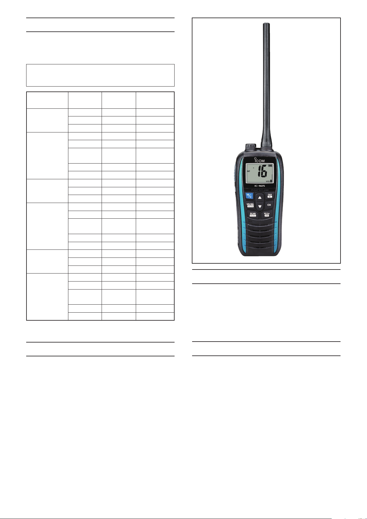
iM25
iM25EURO
S-15208XZ-C1
August 2015
Page 2
INTRODUCTION
This service manual describes the latest technical information for the IC-M25 and IC-M25EURO
time of publication.
To upgrade quality, any electrical or mechanical parts
and internal circuits are subject to change without notice
or obligation.
v h f t r a n s c e i v e r , at the
MODEL
NAME
IC-M25
IC-M25EURO
IC-M25
IC-M25EURO
IC-M25
IC-M25EURO
VERSION
NAME
VERSION
NUMBER
TX OUTPUT
POWER
USA #01 5W/1W
EXP #02 5W/1W
CHN #03 5W/1W
EUR #05 5W/1W
UK #06 5W/1W
FRG #07
5W/1W
(1W/0.5W)
HOL #08 5W/1W
AUS #09 5W/1W
USA-01 #11 5W/1W
EXP-01 #12 5W/1W
CHN-01 #13 5W/1W
EUR-01 #15 5W/1W
UK-01 #16 5W/1W
FRG-01 #17
5W/1W
(1W/0.5W)
HOL-01 #18 5W/1W
AUS-01 #19 5W/1W
USA-02 #21 5W/1W
EXP-02 #22 5W/1W
CHN-02 #23 5W/1W
EUR-02 #25 5W/1W
UK-02 #26 5W/1W
FRG-02 #27
5W/1W
(1W/0.5W)
HOL-02 #28 5W/1W
AUS-02 #29 5W/1W
(IC-M25)
CAUTION
DO NOT reverse the polarities of the power supply when con-
necting the transceiver.
DO NOT apply an RF signal of more than 20 dBm (100 mW) to
the antenna connector. This could damage the transceiver’s
front-end.
ORDERING PARTS
Be sure to include the following four points when ordering
replacement parts:
1. 10-digit Icom part number
2. Component name
3. Equipment model name and unit name
4. Quantity required
<ORDER EXAMPLE>
1110003491 S.IC TA31136FNG IC-M25 MAIN UNIT 5 pieces
8820001210 Screw 2438 screw IC-M25EURO Top cover 10 pieces
Addresses are provided on the inside back cover for your
convenience.
Icom, Icom Inc. and the Icom logo are registered trademarks of Icom Incorporated (Japan) in Japan, the United States, the
United Kingdom, Germany, France, Spain, Russia, Australia, New Zealand, and/or other countries.
1. Make sure that the problem is internal before disassembling the transceiver.
2. DO NOT open the transceiver until the transceiver is dis-
connected from its power source.
3. DO NOT force any of the variable components. Turn them
slowly and smoothly.
4. DO NOT short any circuits or electronic parts. An insulated
tuning tool MUST be used for all adjustments.
5. DO NOT keep power ON for a long time when the trans-
ceiver is defective.
6. DO NOT transmit power into a Standard Signal Generator
or a Sweep Generator, otherwise the RF power may damage them.
7. ALWAYS connect a 30 dB to 40 dB attenuator between the
transceiver and a Deviation Meter or Spectrum Analyzer,
when using such test equipment.
8. READ the instructions of the test equipment thoroughly
before connecting it to the transceiver.
REPAIR NOTES
Page 3

TABLE OF CONTENTS
SECTION 1 SPECIFICATIONS
SECTION 2 INSIDE VIEWS
SECTION 3 DISASSEMBLY INSTRUCTION
SECTION 4 BATTERY PACK REPLACEMENT
SECTION 5 CIRCUIT DESCRIPITON
5-1 RECEIVER CIRCUITS ...................................................................................... 5-1
5-2 TRANSMITTER CIRCUITS ............................................................................... 5-2
5-3 FREQUENCY SYNTHESIZER CIRCUITS ....................................................... 5-3
5-4 VOLTAGE BLOCK DIAGRAM ........................................................................... 5-3
SECTION 6 ADJUSTMENT PROCEDURES
6-1 PREPARATION ................................................................................................. 6-1
6-2 FREQUENCY ADJUSTMENT .......................................................................... 6-2
6-3 RECEIVE ADJUSTMENT ................................................................................. 6-3
6-4 TRANSMIT ADJUSTMENT ............................................................................... 6-3
SECTION 7 PARTS LIST
SECTION 8 MECHANICAL PARTS
SECTION 9 BOARD LAYOUTS
SECTION 10 BLOCK DIAGRAM
SECTION 11 VOLTAGE DIAGRAM
Page 4

SECTION 1 SPECIFICATIONS
M GENERAL
IC-M25 (Except [CHN]) D
• Frequency coverage (MHz):
TX 156.025–157.425
RX 156.050–163.275
• Mode: FM (16K0G3E)
•
Power supply voltage
• Current drain (approximately):
TX (5 W/1.0 W) 2.3 A/0.9 A
Maximum audio (internal SP) 0.30 A
Maximum audio (external SP) 0.20 A
• Frequency stability: ±10 ppm
• Operating temperature:
–20°C to +60°C (–4°F to +140°F)
• Dimensions (projections not included):
56.6 (W) × 134.2 (H) × 30.5 (D) mm,
2.2 (W) × 5.3 (H) × 1.2 (D) inch
• Weight: 220 g, 7.8 oz (approximately)
IC-M25EURO/IC-M25 only [CHN] D
• Frequency coverage (MHz):
TX 156.000–161.450
156.000–161.600 [HOL]
156.025–157.425 [AUS]
RX 156.000–163.425 [EUR], [FRG], [HOL], [UK] and [CHN]
156.300–162.025 [AUS]
• Mode:
FM (16K0G3E)
• Power supply voltage:
3.7 V DC nominal (negative ground)
• Current drain (approximately):
TX (5.0 W/1.0 W/0.5 W*) 2.3 A/0.9 A/0.7 A*
*For only [FRG]
Maximum audio (internal SP) 0.30 A
Maximum audio (external SP) 0.20 A
• Frequency stability:
±1.5 kHz
±10 ppm [AUS]
• Operating temperature:
–15°C to +55°C [EUR], [FRG], [HOL], [UK] and [CHN]
–10°C to +55°C [AUS]
• Dimensions (projections not included):
56.6 (W) × 134.2 (H) × 30.5 (D) mm,
2.2 (W) × 5.3 (H) × 1.2 (D) inch
• Weight (approximately):
220 g, 7.8 oz (including the supplied antenna and belt clip)
: 3.7 V DC nominal (negative ground)
(including the supplied antenna and belt clip)
[EUR], [FRG], [UK] and [CHN]
[EUR], [FRG], [HOL], [UK] and [CHN]
M TRANSMITTER
IC-M25 (Except [CHN]) D
• Output power: 5 W (approximately)/1 W
• Modulation system: Variable reactance frequency modulation
• Maximum frequency deviation:
±5 kHz
• Adjacent channel power:
70 dB
• Spurious emissions: –68 dBc typical
• Residual modulation: 40 dB
• Audio frequency response:
+1 dB to –3 dB of 6 dB octave from 300–3000 Hz
IC-M25EURO/IC-M25 only [CHN] D
• Output power: 5 W (approximately)/1 W/0.5 W*
*For only [FRG]
• Modulation system: Variable reactance frequency modulation
• Maximum frequency deviation:
±5 kHz
• Adjacent channel power:
70 dB
• Spurious emissions:
0.25 µW
0.25 µW typical [AUS]
• Residual modulation: 40 dB
• Audio frequency response:
+1 dB to –3 dB of 6 dB octave from 300–3000 Hz
[EUR], [FRG], [HOL], [UK] and [CHN]
M RECEIVER
IC-M25 (Except [CHN]) D
• Sensitivity : 0.25 µV (–12 dBµ) typical (at 12 dB SINAD)
• Squelch sensitivity: 0.25 µV (–12 dBµ) typical (at threshold)
• Intermodulation: 70 dB typical
• Spurious response: 70 dB typical
•
Adjacent channel selectivity
70 dB typical
• Audio output impedance:
12 Ω (internal speaker)
4 Ω (external speaker)
• Audio output power: Internal SP 0.55 W typical
(at 10% distortion) External SP 0.30 W typical
IC-M25EURO/IC-M25 only [CHN] D
• Sensitivity : –6 dBµ emf typical (at 20 dB SINAD)
• Squelch sensitivity: –6 dBµ emf typical (at threshold)
• Intermodulation: 68 dB [EUR], [FRG], [HOL], [UK] and [CHN]
65 dB [AUS]
• Spurious response: 70 dB [EUR], [FRG], [HOL], [UK] and [CHN]
65 dB [AUS]
•
Adjacent channel selectivity
70 dB [EUR], [FRG], [HOL], [UK] and [CHN]
65 dB [AUS]
• Audio output impedance:
12 Ω (internal speaker)
4 Ω (external speaker)
• Audio output power: Internal SP 0.55 W typical (at 1 kHz)
(at 10% distortion) External SP 0.20 W
:
:
1-1
Page 5

SECTION 2 INSIDE VIEWS
• MAIN UNIT
(TOP VIEW)
LOCK VOLTAGE BUFFER
(IC400)
AF SW
(IC260)
LITHIUM BATTERY CHARGER
(IC601)
???????
(???)
???????
(???)
???????
(???)
2-1
Page 6
VCO
• MAIN UNIT
(TOP VIEW)
???????
(???)
D/A CONVERTER
(IC190)
AF AMP
(IC364)
AF POWER AMP
(IC362)
CPU CLOCK
(X360)
EEPROM
(IC340)
DUAL OP AMP
(IC365)
1st IF FILTER
(FI151)
PLL IC
(IC1)
REFERENCE
FREQUENCY
OSCILLATOR
(X1)
DISCRIMINATOR
(X170)
2nd IF FILETR
(FI170)
IF IC
(IC170)
DRIVE AMP
(Q53)
???????
(???)
RESET
(IC341)
+3 V REGULATOR
(IC220)
QUAD OP AMP
(IC200)
???????
(???)
???????
(???)
TX POWER AMP
(Q54)
1st IF FILTER
(FI150)
TX POWER AMP
(Q55)
???????
(???)
???????
(???)
2-2
Page 7

CLAMP CABLE
INLINE CABLE
インラインケーブル
フラット
ケーブル
フラット
ケーブル
ロックをはずすまっすぐ引き抜く
フラットケーブル
FLAT CABLE
Lift up
flat cable
フラットケーブル
起こす
フラットケーブル
FLAT
CABLE
クランプケーブル
フラット
ケーブル
フラット
ケーブル
SPEAKER
CABLE
スピーカー
ケーブル
UNSOLDER
Solder
remover
ハンダ除去
ハンダ吸取器
Remove with;
flat cable
Release the locks
Pull straight
FLAT CABLE
Flat cable
Flat cable
BE CAREFUL about the locks.
COAXIAL CABLE
同軸ケーブル
Front panel
MAIN UNIT
CLAMP CABLE
FLAT
CABLE
クランプケーブル
フラット
ケーブル
フラット
ケーブル
UNSOLDER
Solder
remover
ハンダ除去
ハンダ吸取器
Remove with;
“ICOM Driver (A)” (8960000020)
“ICOM Driver (AA)” (8960000510)
“ICOM Driver (AE)” (8960000540)
“ICOM Driver (AG)” (8960000560)
“ICOM Driver (G)” (8960000080)
“ICOM Driver (I)” (8960000010)
“ICOM Driver (K)” (8960000110)
“ICOM Driver (K2)” (8960000112)
“ICOM Driver (L2)” (8960000171)
“ICOM Driver (M)” (8960000240)
“ICOM Driver (Q)” (8960000370)
“ICOM Driver (R)” (8960000320)
“ICOM Driver (S)” (8960000410)
“ICOM Driver (T)” (8960000400)
“ICOM Driver (U)” (8960000420)
“ICOM Driver (Y)” (8960000460)
Front panel
MAIN UNIT
FFC
FLAT
CABLE
フラット
ケーブル
フラット
ケーブル
UNSOLDER
Solder
remover
UNSOLDER
Solder
remover
ハンダ除去
ハンダ吸取器
Remove with;
Remove with;
“ICOM Driver (A)” (8960000020)
“ICOM Driver (AA)” (8960000510)
“ICOM Driver (AE)” (8960000540)
“ICOM Driver (AG)” (8960000560)
“ICOM Driver (G)” (8960000080)
“ICOM Driver (I)” (8960000010)
“ICOM Driver (K)” (8960000110)
“ICOM Driver (K2)” (8960000112)
“ICOM Driver (L2)” (8960000171)
“ICOM Driver (M)” (8960000240)
“ICOM Driver (Q)” (8960000370)
“ICOM Driver (R)” (8960000320)
“ICOM Driver (S)” (8960000410)
“ICOM Driver (T)” (8960000400)
“ICOM Driver (U)” (8960000420)
“ICOM Driver (Y)” (8960000460)
Front panel
MAIN UNIT
FFC
CABLE
フラット
ケーブル
フラット
ケーブル
UNSOLDER
Solder
remover
“ICOM Driver (AG)” (8960000560)
“ICOM Driver (G)” (8960000080)
“ICOM Driver (I)” (8960000010)
“ICOM Driver (K)” (8960000110)
“ICOM Driver (K2)” (8960000112)
“ICOM Driver (L2)” (8960000171)
“ICOM Driver (M)” (8960000240)
“ICOM Driver (Q)” (8960000370)
“ICOM Driver (R)” (8960000320)
“ICOM Driver (S)” (8960000410)
“ICOM Driver (T)” (8960000400)
“ICOM Driver (U)” (8960000420)
“ICOM Driver (Y)” (8960000460)
Front panel
MAIN UNIT
MAIN UNIT
3 screws
CHASSIS
CLAMP CABLE
インラインケーブル
FFC
フラット
ケーブル
フラット
ケーブル
ロックをはずすまっすぐ引き抜く
フラットケーブル
FLAT CABLE
Lift up
flat cable
フラットケーブル
起こす
フラットケーブル
FLAT
CABLE
クランプケーブル
フラット
ケーブル
フラット
ケーブル
スピーカー
ケーブル
remover
UNSOLDER
Solder
remover
ハンダ除去
ハンダ吸取器
Remove with;
flat cable
Release the locks
Pull straight
FLAT CABLE
Flat cable
Flat cable
BE CAREFUL about the locks.
同軸ケーブル
Sensor connector
Rear panel
Front panel
MAIN UNIT
3 screws
FFC
フラット
ケーブル
フラット
ケーブル
ロックをはずすまっすぐ引き抜く
フラットケーブル
フラットケーブル
起こす
フラットケーブル
クランプケーブル
フラット
ケーブル
フラット
ケーブル
UNSOLDER
Solder
remover
Rear panel
6 screws
Front panel
MAIN UNIT
MAIN UNIT
3 screws
CHASSIS
SPEAKER
CABLE
SECTION 3 DISASSEMBLY INSTRUCTION
1. Removing the MAIN UNIT
1) Remove the 6 screws from the rear panel.
2) Carefully separate the rear panel, and turn it over in
order to disconnect the battery connector and the
sensor connector.
3) Remove the 6 screws from the MAIN UNIT.
4) Disconnect the speaker cable from the MAIN UNIT.
5) Lift the MAIN UNIT with CHASSIS out of the front
2. Removing the CHASSIS
1) Remove the solder from the antenna connector
2) Disconnect the FFC from the MAIN UNIT.
3) Remove the 3 screws from the MAIN UNIT, and
panel.
conductor.
then remove the CHASSIS.
3-1
Page 8

SECTION 4 BATTERY PACK REPLACEMENT
Ferrite core
Indication lines
Doubled-sided tapes
(Supplied in pair)
Glue
Manufacture: Cemedine Inc.
Name: Super-X
3 to 4 mm
(1/8 to 5/32 inches)
Ferrite core
Glue
Manufacture: Cemedine Inc.
Name: Super-X
3 to 4 mm
(1/8 to 5/32 inches)
Doubled-sided tapes
(Supplied in pair)
Sensor connector
Rear panel
Doubled-sided tapes
(Supplied in pair)
Sensor connector
Rear panel
Ferrite core
Indication lines
Glue
Manufacture: Cemedine Inc.
Name: Super-X
3 to 4 mm
(1/8 to 5/32 inches)
Indication lines
NOTE:
• Before the disassembly, dry the transceiver if it is wet.
• Dispose the old battery pack according to the laws in your
area.
1. Removing the old battery pack
1) Remove the 6 screws from the rear panel.
2) Carefully separate the rear panel and turn it over in
order to disconnect the battery connector and the
red sensor connector.
2. Installing the new battery pack
1) Glue the ferrite core to x its position.
2) Separate the double-sided tapes, which are supplied with the battery pack.
3) Apply the double-sided tapes in the position as
shown below, and then peel the protect sheets.
Pull the old battery pack off the rear panel.
3)
If the double-sided tape is adherent to the rear panel, re-
•
move it.
4) Apply the new battery pack in the position on the
rear panel as shown below.
5) Re-assemble the transceiver.
4-1
Page 9
SECTION 5 CIRCUIT DESCRIPTION
LPF
ANT
SW
ANTENNA
BPF
RF
AMP
BPFBPF
BPFBPF
To 1st mixerFrom RF AMP
D131
D
TX CIRCUITS
92
D52
Q90
D93
D90
D130
T1CON
LPF
ANT
SW
ANTENNA
BPF
RF
AMP
BPFBPF
IF
AMP
BPFBPF
21.7MHz
1st IF signal
FI150,
Q151
To IF IC
To 1st mixerFrom RF AMP
1st LO signals
from VCO
D131
D
TX CIRCUITS
92
D52
Q90
Q150
FI151
D93
D90
D130
T1CON
BPF
RF
AMP
BPFBPF
IF
AMP
X170
450KHz
BPF
LPF
LPF
AF
AMP
X1
21.25MHz
AF
MUTE
21.7MHz
1st IF signal
FI150,
Q151
To IF IC
From 1st IF AMP
To 1st mixerFrom RF AMP
1st LO signals
from VCO
D131
TX CIRCUITS
Q90
IC1
PLL IC
DE ENPHA
IF IC
D/A IC
SPO
AFOUT
J250
Q150
IC170
FI170
450KHz
IC190
IC362
IC365
VOLIN
VOL
BEEP
De-emphasis
R286, C285
SQLO
SQLI
RSSI
NOISE LEVEL
21.25 MHz
2ND LO signal
DET
Int. SP
Ext. SP
FI151
D93
D130
IC260D
DETMS
SP1
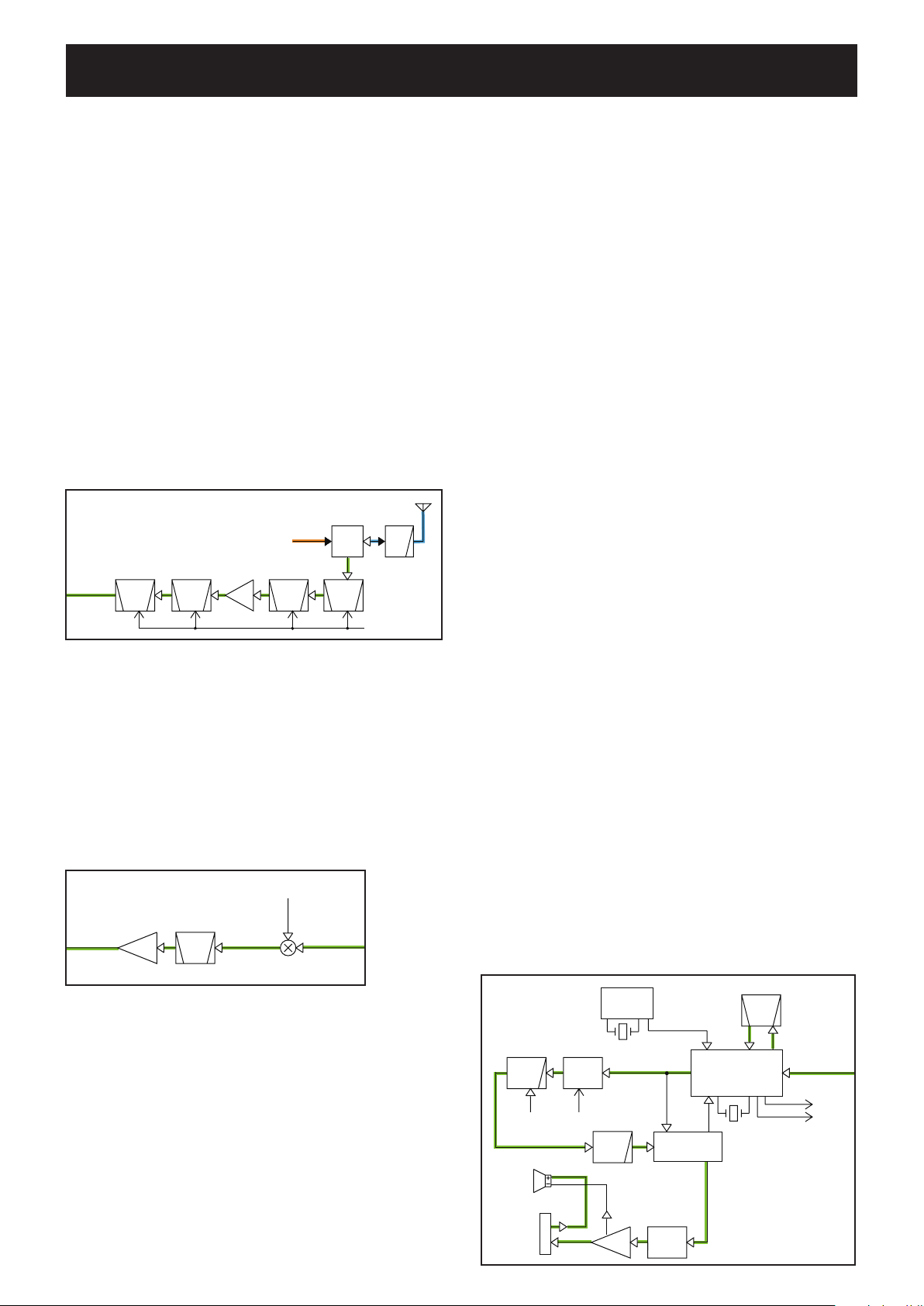
5-1 RECEIVER CIRCUITS
RF CIRCUITS
The RF circuits consist of RF filters, antenna switch, RF
amplier (RF AMP) and so on. The received signal is extract
ed and amplified in the RF circuits.
• ANTENNA SWITCHING CIRCUIT
The RF signal from the antenna is passed through the LPF
(L81, L82, C83–C86 and C89), antenna SW (D52, D90, L90,
C90 and C91) and 2-staged tuned BPF (D92, D93, L92,
L93, C95, C97–C100 and C117), and then applied to the RF
AMP (Q90).
• RF AMPLIFIER
The filtered RX signal is amplified by the RF AMP (Q90)
and passed through another 2-staged BPF (D130, D131,
L96, L97, C109, C110 and C112–L115) to remove unwant-
ed signals. The filtered signal is applied to the 1st mixer
(Q150).
• RF CIRCUITS
2ND IF AND DEMODULATOR CIRCUITS
IC170 is an IF IC which contains the 2nd local oscillator,
2nd mixer, limiter and quadrature detector in its package.
The 21.25 MHz reference frequency signal from the PLL
IC (IC1, pin 9) is applied to the IF IC (IC170, pin 2) as the
2nd LO signal, and it is mixed with 21.7 MHz 1st IF signal
from the 1st IF AMP (Q151), resulting in the 450 kHz 2nd IF
signal. The 450 kHz 2nd IF signal is output from the pin 3 of
IC170.
The 2nd IF signal is filtered by the external ceramic filter
(FI170) which extracts the 450 kHz signal, and then applied
to the internal quadrature detector.
The demodulated AF signal is output from the pin 9.
The quadrature detector is a frequency demodulator which
uses a discriminator (X170) as a phase delayer.
SQUELCH CIRCUIT
A portion of AF signal from the IF IC is adjusted in level by
the D/A converter (IC190), and then applied to the noise
amplifier (IC170, R174–R176, C179 and C180).
Only noise components (approximately 30 kHz signal) are
amplified by the noise amplifier, and then rectified by the
internal noise detector to be converted into DC voltage,
which represents the noise level. The voltage is output from
the pin 14 of IC170, and then applied to the A/D port of the
CPU (IC360, pin 33).
1ST IF CIRCUITS
The RX signal is mixed with the 1st LO signal at the 1st
mixer (Q150), resulting in the 21.7 MHz 1st IF signal. The
converted 1st IF signal is filtered by the crystal filters (FI150
and F151) to remove unwanted out-of-band signals.
The filtered 1st IF signal is amplified by the 1st IF AMP
(Q151), and then applied to the IF demodulate IC (IC170,
pin 16).
• 1ST IF CIRCUITS
The CPU (IC360) compares the applied voltage and squelch
reference level to control the audio signal ON/OFF (emits/
mutes).
RX AF CIRCUITS
The demodulated AF signal from the IF demodulate IC (IC170,
pin 9) is passed through the AF mute SW (IC260D) and LPF
(IC365). The filtered AF signal is de-emphasized by R286 and
C285 to obtain –6 dB/octave of frequency response, and then
applied to the D/A converter (IC190) to be adjusted in level.
The level-adjusted AF signal is amplified by the AF AMP (IC364)
and AF power amplifier (IC362), and then applied to the speaker (CHASSIS: SP1).
• 2ND IF, DEMODULATOR AND RX AF CIRCUITS
5-1
Page 10

5-2 TRANSMITTER CIRCUITS
PWR
AMP
DRIVE
PRE
LO
SW
BUFF
From the VCO
To LO switch
APC
CTRL
BUFFBUFF
LPF
LIMI
T
AMP
MIC
AMP
MIC
MUTE
MIC
MUTE
Q53
Q54
PWR
AMP
Q55
D50
Q50
Q24
Q23
Q 21,Q22
MOD
MUTE
PRE
ENPHA
D/A
VCO
D91
Q20
IC50
IC190
IC200A
IC200D
IC200B
MIC
PWR
SPLITTER
PWR
COMBINER
D20
D
21
D22,D23
INMIC
MOD
IC260A
IC260C
MC250
Q357
PCON
LPF
ANT
SW
ANTENNA
PWR
AMP
DRIVE
PRE
LO
SW
BUFF
APC
CTRL
Receive circuits
D52,D90
Q53
Q54
PWR
AMP
Q55
D50
Q50
PWR
DET
D91
IC50
PWR
SPLITTER
PWR
COMBINER
Q357
PCON
TX AF CIRCUITS
The AF signal from the microphone (MIC signals) is passed
through the MIC mute SW (IC260A), amplified by MIC AMP
(IC200B), and then applied to the D/A converter (IC190),
through another MIC mute SW (IC260C).
TX AMPLIFIERS
The frequency-modulated signal from the VCO (Q21, Q22,
D22 and D23) is passed through the buffers (Q23 and Q24)
and LO SW (D50), and then sequentially amplified by the
buffer AMP (Q50) and pre-drive AMP (Q53).
The level-adjusted MIC signal is pre-emphasized by R201
and C385 to obtain +6 dB/octave of frequency response,
and then passed through the limiter (IC200A) to prevent
over deviation. The amplitude-limited MIC signal is filtered by
the splatter filter (IC200D), which removes 3 kHz and higher
signals, and then applied to the VCO (Q21, Q22, D22 and
D23) for frequency modulation.
• TX AF AND MODULATION CIRCUITS
The amplified signal is splitted by the power splitter (L100,
L101, R463, C445 and C446) and applied to the power
AMPs (Q54 and Q55). The amplified signals are combined
at the power combiner (L107, L108, R465, C457 and C458)
to obtain the TX output power.
The amplified TX signal is passed through the ANT SW
(D52) and LPF (L81, L82, C83–C86 and C89), and then
applied to the antenna.
APC CIRCUIT
A portion of TX output signal is rectified by D91 to produce
the DC voltage which represents the TX power level.
The APC AMP (IC50) compares the voltage and TX power
setting voltage from the D/A converter (IC190). The resulted
voltage from the APC AMP controls the gain of both driver
AMP (Q53) and power AMPs (Q54 and Q55), to keep the TX
output power constant.
• TX AMPLIFIERS AND APC CIRCUIT
5-2
Page 11

5-3 FREQUENCY SYNTHESIZER CIRCUITS
LO
SW
BUFFBUFF
BUFF
FIL
LOOP
X1
21.25 MHz
1st mixer
D 50,D51
Q24Q23
Q25
Q 21,Q22
IC1
PLL IC
IF IC
CPU
VCO
Q150
TX AMPs
IC170IC360
PLLO
2ND LO
D22,D23
PLL control signal
*V
+***V
CHARGE
CTRL
IC601
VCCHV
5.0 V DC
R3V
SW
Q221
R3V
T3V
SW
Q222
T3V
3V
regulator
Q224, Q225
M3V
: To the TX/RX common circuits
: To the RX circuits
: To CPU and EEPROM
: To the TX circuits
3V
regulator
IC220
CPU3V
PWR
CTRL
Q353
CHASSIS
Battery
pack
DC-IN
(USB)
MAIN UNIT
VCO
While transmitting, the oscillation frequency of the VCO
(Q21, Q22, D22 and D23) is determined by the value of
D22, D23, L22, C26 and C27, adding modulation signal to
D20 modulates the oscillating signal.
PLL
IC1 is a PLL IC which contains the pre-scaler, programmable
counter, phase comparator and charge pump in its package.
The 21.25 MHz reference frequency signal is fed from X1.
The generated signal is passed through the buffers (Q23
and Q24), and then applied to the pre-drive AMP (Q53),
through the LO SW (D50) and buffer (Q50).
While receiving, the generated signal is passed through the
buffers (Q23 and Q24), and then applied to the 1st mixer
(Q150), through the LO SW (D51).
• FREQUENCY SYNTHESIZER CIRCUITS
5-4 VOLTAGE BLOCK DIAGRAM
The loop filter is composed by R10, R22, C11, C13 and C24.
5-3
Page 12

SECTION 6 ADJUSTMENT PROCEDURE
to the antenna connector
RF power meter
0.1–6 W/50 Ω
Frequency
counter
Standard signal generator
–20 to 90 dBµ
(–127 dBm to –17 dBm)
DO NOT transmit while
an SSG is connected to
the antenna connector.
To [SP/MIC]
PC
to USB port
OPC-478UC
(USB type)
Modified
OPC-1655
6-1 PREPARATION
M REQUIRED EQUIPMENTS
EQUIPMENT GRADE AND RANGE EQUIPMENT GRADE AND RANGE
Cloning software
RF power meter
(50 Ω terminated)
M CONNECTION
ADJ-M25/M25EURO (Revision 1.0 or later)
Measuring range: 0.1–6 W
Frequency range: 100–300 MHz
SWR: Less than 1.2 : 1
Cables OPC-478UC and OPC-1655
Frequency range: 0.1–300 MHz
Frequency counter
Standard signal
generator (SSG)
Frequency accuracy: ±1 ppm or better
Input level: Less than 1 mW
Frequency range: 0.1–300 MHz
Output level: –20 dBµ to 90 dBµ
(–127 to –17 dBm)
6-1
Page 13

ADJUSTMENT CONDITION
REFERENCE FREQUENCY
TX OUTPUT POWER
RX SENSITIVITY
SQUELCH
M ADJUSTMENT UTILITY SCREEN
• I/O Check screen
(The values shown above are exsample only.
Each transceiver has own values.)
The Lock Voltage is displayed here.
6-2 FREQUENCY ADJUSTMENTS
1) Select an adjustment item using [↑]/[↓] on the PC's keyboard.
2) Set or modify the adjustment value as specified using [←]/[→] on the PC's keyboard, and then push [ENTER].
ADJUSTMENT
PLL LOCK
VOLTAGE
VERIFICATION
REFERENCE
FREQUENCY
TRANSCEIVER’S
CONDITION
1 • CH.: 16
• Receiving
2 • CH.: 16
• Transmitting
1 • CH.: 16
• Transmitting
OPERATION
1) C onnec t an RF power met er to the
antenna connector.
2) Click the [Update (F5)] button to check on
the "I/O Check screen" as below.
• Loosely couple a frequency counter to the
antenna connector. [Ref. Freq.]
ADJUSTMENT
ITEM
[LVIN]
(On the "I/O
Check screen")
VALUE
1.65 V ±0.5 V
1.70 V ±0.5 V
156.800000
MHz
(±500 Hz)
6-2
Page 14

6-3 RECEIVE ADJUSTMENTS
1) Select an adjustment item using [↑]/[↓] on the PC's keyboard.
2) Set or modify the adjustment value as specified using [←]/[→] on the PC's keyboard, and then push [ENTER].
ADJUSTMENT
RX SENSITIVITY
SQUELCH 1 NOTE: When "RX SENSITIVITY" must be adjusted before "SQUELCH." And when "RX SENSITIVITY" is
†
The output level of the standard signal generator (SSG) is indicated as the SSG’s open circuit.
TRANSCEIVER’S
CONDITION
1 NOTE: When "RX SENSITIVITY" is re-adjusted, "SQUELCH" must be re-adjusted too.
• CH.: 16
• Receiving
re-adjusted, "SQUELCH" must be re-adjusted too.
• CH.: 16
• Receiving
• Connect an SSG to the antenna connector and
set it as;
Frequency: 156.800 MHz
Level
Modulation: 1 kHz
Deviation: ±3.0 kHz
• Connect an SSG to the antenna connector and
Frequency: 156.800 MHz
Level
Modulation: 1 kHz
Deviation: ±3.0 kHz
set it as;
†
: +30 dBµ (–77 dBm)
†
: –4 dBµ
OPERATION
(–111 dBm)
ADJUSTMENT
ITEM
[BPF]
[Noise]
VALUE
Push [ENTER]
on [BPF].
(Automatic
adjustment)
Push [ENTER]
on [Noise].
(Automatic
adjustment)
6-4 TRANSMIT ADJUSTMENTS
1) Select an adjustment item using [↑]/[↓] on the PC's keyboard.
2) Set or modify the adjustment value as specified using [←]/[→] on the PC's keyboard, and then push [ENTER].
ADJUSTMENT
TX OUTPUT
POWER
(High)
(L_High)* 2 [RF Power (L_High)] 2.5 W
(Low) 3 [RF Power (Low)] 0.75 W
(E_Low)* 4 [RF Power (E_Low)] 0.45 W
*For only [FRG] version.
TRANSCEIVER’S
CONDITION
1 • CH.: 16
• Transmitting
OPERATION
• Connect an RF power meter to the
antenna connector. [RF Power (High)]
ADJUSTMENT
ITEM
VALUE
4.5 W
6-3
Page 15

SECTION 7. PARTS LIST
[MAIN UNIT]
REF PARTS
NO. NO.
IC1 1130016080 S.IC GP214D <SEI> B 39.6/11.3
IC50 1110008890 S.IC NJU7056F3-TE2-#ZZZH T 105.1/20.3
IC170 1110007320 S.IC NJM2591V-TE1-#ZZZB B 17.7/8.9
IC190 1110007550 S.IC R2A20178NP B 43.6/33.4
IC200 1110008830 S.IC NJU7058V-TE2-#ZMZH B 10.7/38.4
IC220 1180004720 S.REG S-1335J30-M5T1U3 B 104.6/38.7
IC260 1130015760 S.IC TC74VHC4066AFK(EK) T 31.9/41.1
IC340 1130016621 S.IC GT24C128B-2ZLI-TR <MSK> B 110.9/29.9
IC341 1110008930 S.IC NJU7704F3-03A-TE1-#ZZZH B 103.8/35.8
IC360 1140017430 S.IC UPD78F0338GC-9EB-A
(FX-3723A) T 105.7/34.5
IC362 1110007610 S.IC TPA0211DGNR B 50.9/39.5
IC364 1110008890 S.IC NJU7056F3-TE2-#ZZZH B 46.7/39.3
IC365 1110008940 S.IC NJU7057RB1-TE2-#ZMZH B 35.2/35.8
IC400 1110008890 S.IC NJU7056F3-TE2-#ZZZH T 36.0/5.2
IC601 1190004140 S.IC APM8600FB-7 <TKC> T 22.0/37.6
Q20 1590004070 S.TRA LDTC144EET1G <SLVJ> B 50.9/15.0
Q21 1530004011 S.TRA KTC3770U-C-RTK/P B 58.0/15.2
Q22 1530004011 S.TRA KTC3770U-C-RTK/P B 59.0/11.7
Q23 1530002381 S.TRA 2SC4215-Y(TE85LF) B 55.7/19.6
Q24 1530002381 S.TRA 2SC4215-Y(TE85LF) B 60.9/21.6
Q25 1530002381 S.TRA 2SC4215-Y(TE85LF) B 52.2/21.6
Q50 1530004011 S.TRA KTC3770U-C-RTK/P B 69.2/18.8
Q53 1560001910 S.FET RD01MUS2B-T113 B 69.4/13.2
Q54 1560001701 S.FET RD07MUS2B-T214 B 79.5/9.3
Q55 1560001701 S.FET RD07MUS2B-T214 B 79.5/17.4
Q90 1580000751 S.FET 3SK294(TE85LF) B 94.6/20.0
Q150 1580000731 S.FET 3SK293(TE85LF) B 69.7/27.9
Q151 1530002601 S.TRA 2SC4215-O(TE85RF) T 28.1/8.8
Q221 1590005220 S.TRA LDTA114YET1G <SLVJ> B 61.0/35.6
Q222 1590005220 S.TRA LDTA114YET1G <SLVJ> B 63.0/35.6
Q224 1590003800 S.TRA KTC811U-GR-RTK/P B 55.3/42.8
Q225 1520000910 S.TRA 2SB1132L-R-AB3-R <SLVJ> B 59.2/43.3
Q230 1550000090 S.FET RSQ035P03TR B 49.9/45.5
Q231 1590003800 S.TRA KTC811U-GR-RTK/P B 45.8/46.0
Q240 1590004230 S.TRA LMUN5213DW1T1G <SLVJ> T 95.2/29.0
Q250 1590004070 S.TRA LDTC144EET1G <SLVJ> B 33.7/41.8
Q251 1510001100 S.TRA 2SA1832-GR(TE85RF) B 86.3/43.9
Q350 1590004100 S.TRA LDTC144TET1G <SLVJ> B 91.6/32.8
Q351 1590004050 S.TRA LDTA144EET1G <SLVJ> T 107.5/20.9
Q353 1550000090 S.FET RSQ035P03TR B 66.8/40.4
Q354 1590004070 S.TRA LDTC144EET1G <SLVJ> B 77.0/37.6
Q357 1590004070 S.TRA LDTC144EET1G <SLVJ> T 104.2/22.8
Q362 1590004070 S.TRA LDTC144EET1G <SLVJ> B 61.1/8.2
Q365 1590004050 S.TRA LDTA144EET1G <SLVJ> T 106.4/16.1
Q366 1590004070 S.TRA LDTC144EET1G <SLVJ> B 55.8/40.5
Q603 1590004070 S.TRA LDTC144EET1G <SLVJ> T 27.9/36.8
Q606 1550000090 S.FET RSQ035P03TR B 63.4/40.5
Q608 1550000410 S.FET SSM3J35FS(TE85LF) B 77.4/42.5
Q609 1590004230 S.TRA LMUN5213DW1T1G <SLVJ> B 78.3/39.9
D1 1750001770 S.VAR 1SV323(TPH3F) B 29.9/11.0
D3 1750001810 S.DIO L1SS400T1G <SLVJ> B 42.8/14.7
D20 1750002920 S.DIO KDS114E-RTK/PA B 48.3/14.1
D21 1750002920 S.DIO KDS114E-RTK/PA B 50.2/16.7
D22 1750003330 S.VAR BBY58-02V H6327 <RYOYO> B 58.3/8.3
D23 1750003330 S.VAR BBY58-02V H6327 <RYOYO> B 59.5/8.3
D50 1750002780 S.DIO RN142GT2R B 68.3/23.0
D51 1750002780 S.DIO RN142GT2R B 68.3/24.1
D52 1750000581 S.DIO 1SV307(TPH3F) B 105.7/8.0
D90 1750002920 S.DIO KDS114E-RTK/PA B 104.6/16.2
D91 1790001670 S.DIO RB706F-40T106 T 99.6/15.8
D92 1750003270 S.VAR BB174X <RYO> B 102.5/19.5
D93 1750003270 S.VAR BB174X <RYO> B 98.5/20.4
D130 1750003270 S.VAR BB174X <RYO> B 90.7/23.3
D131 1750003270 S.VAR BB174X <RYO> B 86.3/25.7
D200 1790001670 S.DIO RB706F-40T106 T 102.1/15.9
D350 1750001180 S.DIO KDS122 RTK/P B 94.0/33.3
D353 1750002170 S.DIO DB2S31400L B 105.4/14.5
D356 1750001810 S.DIO L1SS400T1G <SLVJ> B 46.6/42.7
D357 1790001860 S.VAR EZJZ0V80010 B 78.0/21.4
D358 1750001850 S.DIO LDAN222T1G <SLVJ> B 65.8/43.1
D609 1750001810 S.DIO L1SS400T1G <SLVJ> B 61.0/40.6
D610 1750002110 S.DIO LRB551V-30T1G <SLVJ> B 62.6/44.3
D613 1790001810 S.VAR AVR-M1005C080MTABB B 78.8/42.9
FI150 2030000350 MON 21R15AB (FL-368)
FI151 2030000481 MON 21R15AB (FL-399A)
FI170 2020002410 CER LTM450FW <JJE>
X1 6050011740 S.XTA CR-766 XRCMK 21.250 MHz B 31.4/6.9
X170 6070000310 S.DIS JTBM450CX70 <JJE> B 25.6/6.1
X360 6050013200 S.XTA CR-911(HC49U/SM 4.9152 MHz
<SKD> B 92.3/39.2
L1 6200003711 S.COI NLV25T-2R7J-PF T 24.4/5.0
L20 6200011021 S.COI ELJRF 82NJFB *0 B 50.1/20.9
L21 6200002861 S.COI NLV25T-4R7J-PF B 48.9/9.5
L22 6200009910 S.COI C6342A-88NG-A B 53.6/10.4
L23 6200011031 S.COI ELJRF R10JFB *0 B 57.5/19.9
L24 6200011031 S.COI ELJRF R10JFB *0 B 59.6/20.2
L25 6200011031 S.COI ELJRF R10JFB *0 B 52.6/19.6
DESCRIPTION
Eqv.= This component is equivalent to the REF No. component listed above, and
may be substituted on parts orders and repairs.
M.
H/V
LOCATION
[MAIN UNIT]
REF PARTS
NO. NO.
L26 6200011021 S.COI ELJRF 82NJFB *0 B 68.6/26.0
L50 6200011031 S.COI ELJRF R10JFB *0 B 70.6/20.2
L51 6200011021 S.COI ELJRF 82NJFB *0 B 71.2/16.6
L53 6200006981 S.COI ELJRE R10GFA *0 B 70.5/10.0
L55 6200012680 S.COI 0.30-1.3-5TL 20N <COMO> B 84.5/11.8
L56 6200012390 S.COI 0.30-0.92-3TR 5.8N <COMO> B 87.1/10.5
L57 6200012680 S.COI 0.30-1.3-5TL 20N <COMO> B 89.6/9.6
L58 6200003711 S.COI NLV25T-2R7J-PF B 102.3/9.7
L80 6200012470 S.COI 0.30-1.7-7TL 45.3N <COMO> B 99.0/8.3
L81 6200012770 S.COI 0.26-1.1-7TR 24N <COMO> B 110.4/9.3
L82 6200012780 S.COI 0.30-1.4-6TL 27.2N <COMO> B 110.9/12.3
L90 6200012470 S.COI 0.30-1.7-7TL 45.3N <COMO> B 106.2/11.9
L92 6200007750 S.COI LQW2BHN56NJ03L B 102.0/16.6
L93 6200007750 S.COI LQW2BHN56NJ03L B 98.2/17.4
L96 6200007750 S.COI LQW2BHN56NJ03L B 92.3/22.3
L97 6200007750 S.COI LQW2BHN56NJ03L B 84.0/24.3
L98 6200003680 S.COI LQH31MNR82M03L B 62.5/28.6
L99 6200011001 S.COI ELJRF 56NJFB *0 B 72.8/10.0
L100 6200010991 S.COI ELJRF 47NJFB *0 B 74.7/12.9
L101 6200010991 S.COI ELJRF 47NJFB *0 B 74.7/13.8
L102 6200007901 S.COI ELJRF 22NJFB *0 B 75.9/9.4
L103 6200007901 S.COI ELJRF 22NJFB *0 B 75.9/17.4
L104 6200012680 S.COI 0.30-1.3-5TL 20N <COMO> B 85.0/20.5
L105 6200012390 S.COI 0.30-0.92-3TR 5.8N <COMO> B 84.0/17.7
L106 6200012680 S.COI 0.30-1.3-5TL 20N <COMO> B 87.2/18.1
L107 6200012470 S.COI 0.30-1.7-7TL 45.3N <COMO> B 94.1/11.0
L108 6200012470 S.COI 0.30-1.7-7TL 45.3N <COMO> B 94.6/14.8
R1 7510001730 S.THE ERTJOEP 473J B 39.5/17.8
R2 7030012480 S.RES ERJ2RKF 1003X (100K) B 41.6/17.0
R3 7030005050 S.RES ERJ2GEJ 103 X (10K) B 33.4/12.2
R4 7030005240 S.RES ERJ2GEJ 473 X (47K) B 32.2/11.8
R5 7030005050 S.RES ERJ2GEJ 103 X (10K) B 34.7/8.2
R6 7030005240 S.RES ERJ2GEJ 473 X (47K) B 53.7/15.1
R7 7030005000 S.RES ERJ2GEJ 471 X (470) B 52.8/14.2
R10 7030008370 S.RES ERJ2GEJ 561 X (560) B 39.4/7.6
R20 7030004980 S.RES ERJ2GEJ 101 X (100) B 48.6/20.6
R22 7030005040 S.RES ERJ2GEJ 472 X (4.7K) B 41.5/8.0
R23 7030004990 S.RES ERJ2GEJ 221 X (220) B 49.4/13.7
R24 7030005090 S.RES ERJ2GEJ 104 X (100K) B 49.8/17.8
R25 7030005090 S.RES ERJ2GEJ 104 X (100K) B 48.6/17.0
R26 7030005290 S.RES ERJ2GEJ 682 X (6.8K) B 58.4/16.9
R27 7030005210 S.RES ERJ2GEJ 822 X (8.2K) B 60.1/13.4
R28 7030004980 S.RES ERJ2GEJ 101 X (100) B 58.5/13.4
R30 7030005070 S.RES ERJ2GEJ 683 X (68K) B 56.5/16.8
R31 7030004990 S.RES ERJ2GEJ 221 X (220) B 57.9/18.7
R32 7030007270 S.RES ERJ2GEJ 151 X (150) B 58.4/19.9
R33 7030007350 S.RES ERJ2GEJ 393 X (39K) B 59.1/22.0
R34 7030008280 S.RES ERJ2GEJ 271 X (270) B 53.9/19.2
R35 7030007350 S.RES ERJ2GEJ 393 X (39K) B 53.9/21.3
R36 7030005710 S.RES ERJ2GEJ 121 X (120) B 58.6/26.8
R47 7030009140 S.RES ERJ2GEJ 272 X (2.7K) T 30.0/6.1
R50 7030005120 S.RES ERJ2GEJ 102 X (1K) B 67.0/22.1
R52 7030007290 S.RES ERJ2GEJ 222 X (2.2K) B 70.2/23.0
R53 7030004980 S.RES ERJ2GEJ 101 X (100) B 70.7/21.8
R54 7030005530 S.RES ERJ2GEJ 100 X (10) B 69.5/21.5
R55 7030007300 S.RES ERJ2GEJ 332 X (3.3K) B 69.4/20.6
R56 7030007570 S.RES ERJ2GEJ 122 X (1.2K) B 67.0/18.5
R57 7030005590 S.RES ERJ2GEJ 680 X (68) B 67.0/19.4
R65 7030005100 S.RES ERJ2GEJ 154 X (150K) T 102.2/23.0
R66 7030005070 S.RES ERJ2GEJ 683 X (68K) T 103.2/20.6
R67 7030005310 S.RES ERJ2GEJ 124 X (120K) T 103.2/19.0
R68 7030004980 S.RES ERJ2GEJ 101 X (100) T 105.4/17.6
R69 7030005090 S.RES ERJ2GEJ 104 X (100K) B 67.0/15.7
R70 7030005100 S.RES ERJ2GEJ 154 X (150K) B 68.8/16.8
R71 7030004970 S.RES ERJ2GEJ 470 X (47) B 70.0/16.2
R73 7030005050 S.RES ERJ2GEJ 103 X (10K) B 75.9/6.2
R74 7030005720 S.RES ERJ2GEJ 563 X (56K) B 74.7/7.6
R75 7030004980 S.RES ERJ2GEJ 101 X (100) B 75.9/7.8
R76 7030000260 S.RES MCR10EZHJ 100 (101) B 101.9/13.1
R80 7030005080 S.RES ERJ2GEJ 823 X (82K) B 114.6/12.6
R81 7030005090 S.RES ERJ2GEJ 104 X (100K) T 99.7/20.6
R91 7030005110 S.RES ERJ2GEJ 224 X (220K) B 101.5/20.9
R93 7030005050 S.RES ERJ2GEJ 103 X (10K) B 99.7/22.8
R94 7030005110 S.RES ERJ2GEJ 224 X (220K) B 99.7/21.2
R95 7030005310 S.RES ERJ2GEJ 124 X (120K) B 96.5/20.7
R96 7030005700 S.RES ERJ2GEJ 274 X (270K) B 96.3/18.3
R97 7030004990 S.RES ERJ2GEJ 221 X (220) B 94.1/21.8
R103 7030005050 S.RES ERJ2GEJ 103 X (10K) B 97.4/20.7
R104 7030005090 S.RES ERJ2GEJ 104 X (100K) B 90.2/20.5
R105 7030005110 S.RES ERJ2GEJ 224 X (220K) B 89.4/25.3
R107 7030005110 S.RES ERJ2GEJ 224 X (220K) B 88.2/25.7
R109 7030005530 S.RES ERJ2GEJ 100 X (10) B 64.0/27.1
R110 7030008400 S.RES ERJ2GEJ 182 X (1.8K) B 65.2/29.1
R111 7030005080 S.RES ERJ2GEJ 823 X (82K) B 72.3/26.8
R112 7030008010 S.RES ERJ2GEJ 123 X (12K) B 72.3/25.2
R113 7030005530 S.RES ERJ2GEJ 100 X (10) B 97.3/21.9
R115 7030006610 S.RES ERJ2GEJ 394 X (390K) B 67.9/27.4
R120 7030007290 S.RES ERJ2GEJ 222 X (2.2K) B 70.2/25.1
R121 7030005220 S.RES ERJ2GEJ 223 X (22K) B 70.2/26.0
R122 7030005100 S.RES ERJ2GEJ 154 X (150K) B 71.4/26.8
R152 7030005030 S.RES ERJ2GEJ 152 X (1.5K) B 42.7/26.6
R153 7030004990 S.RES ERJ2GEJ 221 X (220) T 35.7/11.0
R154 7030005090 S.RES ERJ2GEJ 104 X (100K) T 29.8/9.0
R155 7030007290 S.RES ERJ2GEJ 222 X (2.2K) T 29.4/11.1
R156 7030005000 S.RES ERJ2GEJ 471 X (470) T 29.4/10.2
R170 7030009280 S.RES ERJ2GEJ 391 X B 26.5/10.8
DESCRIPTION
M.=Mounted side (T: Mounted on the Top side, B: Mounted on the Bottom side)
7-1
M.
S.=Surface mount
H/V
LOCATION
Page 16

[MAIN UNIT]
REF PARTS
NO. NO.
R171 7030009140 S.RES ERJ2GEJ 272 X (2.7K) B 23.2/10.5
R172 7030005000 S.RES ERJ2GEJ 471 X (470) B 21.0/11.9
R173 7030005030 S.RES ERJ2GEJ 152 X (1.5K) B 16.3/5.6
R174 7030005230 S.RES ERJ2GEJ 334 X (330K) B 14.6/11.9
R175 7030005600 S.RES ERJ2GEJ 273 X (27K) B 16.7/12.4
R176 7030005120 S.RES ERJ2GEJ 102 X (1K) B 17.9/13.1
R192 7030009280 S.RES ERJ2GEJ 391 X B 48.2/32.7
R193 7030005000 S.RES ERJ2GEJ 471 X (470) B 44.8/29.7
R194 7030005090 S.RES ERJ2GEJ 104 X (100K) B 47.7/31.4
R201 7030007290 S.RES ERJ2GEJ 222 X (2.2K) B 14.1/41.4
R202 7030005090 S.RES ERJ2GEJ 104 X (100K) B 15.3/39.8
R203 7030005110 S.RES ERJ2GEJ 224 X (220K) B 12.8/41.6
R204 7030005040 S.RES ERJ2GEJ 472 X (4.7K) B 11.9/42.5
R206 7030008290 S.RES ERJ2GEJ 183 X (18K) T 9.4/41.1
R207 7030007350 S.RES ERJ2GEJ 393 X (39K) B 11.2/41.6
R212 7030005030 S.RES ERJ2GEJ 152 X (1.5K) T 7.9/39.9
R213 7030005100 S.RES ERJ2GEJ 154 X (150K) T 7.9/38.3
R214 7030007340 S.RES ERJ2GEJ 153 X (15K) T 6.7/37.7
R226 7030005040 S.RES ERJ2GEJ 472 X (4.7K) B 54.3/40.8
R227 7030005050 S.RES ERJ2GEJ 103 X (10K) B 57.9/46.6
R228 7030008300 S.RES ERJ2GEJ 184 X (180K) B 53.9/44.5
R230 7030005230 S.RES ERJ2GEJ 334 X (330K) B 46.7/44.0
R231 7030007280 S.RES ERJ2GEJ 331 X (330) B 45.8/44.0
R235 7030010010 S.RES ERJ2RKF 334 X (330K) B 64.2/43.0
R236 7030010020 S.RES ERJ2RKF 1503X (150K) B 64.0/45.4
R240 7030004990 S.RES ERJ2GEJ 221 X (220) T 94.7/27.2
R242 7410001270 S.ARR EXB28V821JX B 54.8/32.7
R251 7030008280 S.RES ERJ2GEJ 271 X (270) B 80.9/43.2
R252 7030005060 S.RES ERJ2GEJ 333 X (33K) B 41.2/44.3
R253 7030007300 S.RES ERJ2GEJ 332 X (3.3K) B 16.9/37.4
R255 7030005700 S.RES ERJ2GEJ 274 X (270K) B 15.1/36.5
R256 7030008290 S.RES ERJ2GEJ 183 X (18K) B 15.4/38.6
R257 7030005040 S.RES ERJ2GEJ 472 X (4.7K) B 16.9/35.6
R258 7030005040 S.RES ERJ2GEJ 472 X (4.7K) B 18.1/36.0
R260 7030005110 S.RES ERJ2GEJ 224 X (220K) T 11.6/39.7
R261 7030005720 S.RES ERJ2GEJ 563 X (56K) T 12.5/39.7
R262 7030005240 S.RES ERJ2GEJ 473 X (47K) T 12.5/40.9
R263 7030008290 S.RES ERJ2GEJ 183 X (18K) T 35.8/36.5
R264 7030005090 S.RES ERJ2GEJ 104 X (100K) B 31.4/39.9
R265 7030005090 S.RES ERJ2GEJ 104 X (100K) T 36.1/37.9
R270 7030005120 S.RES ERJ2GEJ 102 X (1K) B 41.2/45.2
R271 7030011650 S.RES ERJ2GEJ 243X (24K) B 33.0/38.3
R272 7030005090 S.RES ERJ2GEJ 104 X (100K) B 35.7/39.4
R273 7030005220 S.RES ERJ2GEJ 223 X (22K) B 35.7/38.5
R276 7030008300 S.RES ERJ2GEJ 184 X (180K) B 38.7/36.6
R277 7030005090 S.RES ERJ2GEJ 104 X (100K) B 38.3/35.3
R278 7030005120 S.RES ERJ2GEJ 102 X (1K) B 37.1/39.1
R279 7030005030 S.RES ERJ2GEJ 152 X (1.5K) B 38.0/39.1
R283 7030005090 S.RES ERJ2GEJ 104 X (100K) B 48.0/48.0
R286 7030008010 S.RES ERJ2GEJ 123 X (12K) B 39.3/38.5
R290 7030007060 S.RES ERJ2GEJ 684X (680K) B 40.9/36.9
R291 7030005090 S.RES ERJ2GEJ 104 X (100K) B 39.5/34.5
R292 7030005090 S.RES ERJ2GEJ 104 X (100K) B 44.5/38.4
R293 7030008010 S.RES ERJ2GEJ 123 X (12K) B 46.6/41.0
R294 7030005040 S.RES ERJ2GEJ 472 X (4.7K) B 48.2/40.9
R295 7030005040 S.RES ERJ2GEJ 472 X (4.7K) B 49.2/42.1
R300 7030005290 S.RES ERJ2GEJ 682 X (6.8K) T 9.9/38.3
R340 7030005090 S.RES ERJ2GEJ 104 X (100K) B 106.3/29.8
R341 7030005050 S.RES ERJ2GEJ 103 X (10K) B 106.3/28.9
R343 7030005050 S.RES ERJ2GEJ 103 X (10K) B 105.7/36.3
R351 7030005120 S.RES ERJ2GEJ 102 X (1K) B 89.8/34.0
R352 7030007340 S.RES ERJ2GEJ 153 X (15K) B 93.3/31.5
R353 7030005120 S.RES ERJ2GEJ 102 X (1K) B 93.3/30.6
R361 7410001130 S.ARR EXB28V102JX T 115.7/31.8
R371 7030005170 S.RES ERJ2GEJ 474 X (470K) T 103.1/45.5
R372 7030007310 S.RES ERJ2GEJ 155 X (1.5M) T 106.3/45.5
R373 7030005160 S.RES ERJ2GEJ 105 X (1M) T 104.7/45.5
R374 7030006610 S.RES ERJ2GEJ 394 X (390K) T 104.0/44.1
R376 7030005090 S.RES ERJ2GEJ 104 X (100K) T 10.7/40.6
R377 7030005080 S.RES ERJ2GEJ 823 X (82K) B 9.1/41.9
R378 7030005080 S.RES ERJ2GEJ 823 X (82K) B 7.4/41.9
R379 7030005080 S.RES ERJ2GEJ 823 X (82K) B 6.4/39.8
R380 7030005050 S.RES ERJ2GEJ 103 X (10K) B 98.0/10.5
R381 7030005050 S.RES ERJ2GEJ 103 X (10K) T 101.4/19.0
R382 7030009140 S.RES ERJ2GEJ 272 X (2.7K) T 100.5/19.0
R383 7030008010 S.RES ERJ2GEJ 123 X (12K) T 101.0/20.2
R384 7030007290 S.RES ERJ2GEJ 222 X (2.2K) T 105.4/18.5
R386 7030005050 S.RES ERJ2GEJ 103 X (10K) T 107.8/22.7
R387 7030005090 S.RES ERJ2GEJ 104 X (100K) B 86.5/45.3
R388 7030005170 S.RES ERJ2GEJ 474 X (470K) T 30.6/36.3
R391 7030005240 S.RES ERJ2GEJ 473 X (47K) B 5.5/40.6
R392 7030007340 S.RES ERJ2GEJ 153 X (15K) B 84.7/44.0
R393 7030007290 S.RES ERJ2GEJ 222 X (2.2K) B 85.4/42.4
R395 7030005090 S.RES ERJ2GEJ 104 X (100K) B 90.5/31.4
R396 7030005050 S.RES ERJ2GEJ 103 X (10K) T 115.7/35.4
R397 7030005700 S.RES ERJ2GEJ 274 X (270K) B 69.1/42.3
R398 7030005050 S.RES ERJ2GEJ 103 X (10K) B 67.9/43.0
R401 7030005090 S.RES ERJ2GEJ 104 X (100K) T 102.6/21.8
R402 7030005060 S.RES ERJ2GEJ 333 X (33K) B 43.3/40.3
R403 7030005050 S.RES ERJ2GEJ 103 X (10K) B 42.2/39.1
R404 7030004980 S.RES ERJ2GEJ 101 X (100) B 41.3/39.1
R410 7030005120 S.RES ERJ2GEJ 102 X (1K) T 99.3/17.8
R411 7030005120 S.RES ERJ2GEJ 102 X (1K) T 100.9/17.8
R412 7030005050 S.RES ERJ2GEJ 103 X (10K) B 5.2/36.9
R413 7030005050 S.RES ERJ2GEJ 103 X (10K) B 6.4/36.5
R414 7030005050 S.RES ERJ2GEJ 103 X (10K) B 6.4/38.2
R415 7030005240 S.RES ERJ2GEJ 473 X (47K) B 5.2/36.0
R430 7030005700 S.RES ERJ2GEJ 274 X (270K) B 47.7/46.4
R431 7030005120 S.RES ERJ2GEJ 102 X (1K) B 47.7/44.8
R432 7030005040 S.RES ERJ2GEJ 472 X (4.7K) B 44.5/39.3
R433 7030005090 S.RES ERJ2GEJ 104 X (100K) B 38.2/33.7
R434 7030005080 S.RES ERJ2GEJ 823 X (82K) B 37.0/33.6
R435 7030008010 S.RES ERJ2GEJ 123 X (12K) B 35.4/33.6
R450 7030007280 S.RES ERJ2GEJ 331 X (330) B 43.5/45.2
R451 7030005040 S.RES ERJ2GEJ 472 X (4.7K) B 46.8/47.7
DESCRIPTION
Eqv.= This component is equivalent to the REF No. component listed above, and
may be substituted on parts orders and repairs.
M.
H/V
LOCATION
[MAIN UNIT]
REF PARTS
NO. NO.
R452 7030007290 S.RES ERJ2GEJ 222 X (2.2K) B 43.9/46.4
R457 7030005050 S.RES ERJ2GEJ 103 X (10K) B 32.2/34.0
R458 7030005040 S.RES ERJ2GEJ 472 X (4.7K) B 32.2/35.6
R459 7030005040 S.RES ERJ2GEJ 472 X (4.7K) B 31.3/35.6
R460 7030004970 S.RES ERJ2GEJ 470 X (47) B 38.7/15.0
R461 7030004990 S.RES ERJ2GEJ 221 X (220) B 61.2/11.5
R462 7030010040 S.RES ERJ2GEJ-JPW B 61.2/9.7
R463 7030004980 S.RES ERJ2GEJ 101 X (100) B 75.9/13.4
R464 7030004980 S.RES ERJ2GEJ 101 X (100) B 75.5/18.6
R465 7030003320 S.RES ERJ3GEYJ 101 V (100) B 91.0/13.9
R466 7030005050 S.RES ERJ2GEJ 103 X (10K) B 75.0/17.4
R467 7030005720 S.RES ERJ2GEJ 563 X (56K) B 73.8/17.0
R468 7030004990 S.RES ERJ2GEJ 221 X (220) T 94.7/26.3
R477 7030005050 S.RES ERJ2GEJ 103 X (10K) T 102.8/17.8
R478 7030005050 S.RES ERJ2GEJ 103 X (10K) B 41.6/46.4
R479 7030007340 S.RES ERJ2GEJ 153 X (15K) B 99.9/10.5
R607 7030014270 S.RES ERJ2RKF3300X (330) T 17.5/38.3
R608 7030014260 S.RES ERJ2RKF1801X T 19.1/38.3
R609 7030005050 S.RES ERJ2GEJ 103 X (10K) T 28.5/38.7
R634 7030005050 S.RES ERJ2GEJ 103 X (10K) T 115.1/37.5
R641 7030010010 S.RES ERJ2RKF 334 X (330K) T 28.3/40.3
R642 7030010020 S.RES ERJ2RKF 1503X (150K) T 28.3/41.9
R647 7030005050 S.RES ERJ2GEJ 103 X (10K) B 60.2/39.1
R650 7030005160 S.RES ERJ2GEJ 105 X (1M) B 79.7/43.3
R659 7030004980 S.RES ERJ2GEJ 101 X (100) B 3.4/29.8
C2 4030017460 S.CER C1005 JB 1H 102K-T B 31.0/12.1
C3 4030017440 S.CER C1005 CH 1H 221J-T B 33.1/11.0
C4 4030017640 S.CER C1005 CH 1H 150J-T B 31.9/10.6
C5 4030017670 S.CER C1005 CH 1H 390J-T B 35.9/8.3
C6 4030017460 S.CER C1005 JB 1H 102K-T B 53.3/16.3
C7 4030018860 S.CER C1005 JB 0J 105K-T B 39.9/14.6
C8 4030017350 S.CER C1005 CH 1H 020B-T T 26.6/5.1
C9 4030017350 S.CER C1005 CH 1H 020B-T T 22.2/5.1
C11 4550007480 S.TAN F930J106MAABMA B 36.7/5.2
C12 4030017460 S.CER C1005 JB 1H 102K-T T 20.8/5.6
C13 4030016930 S.CER C1005 JB 1A 104K-T B 40.3/7.6
C15 4030016790 S.CER C1005 JB 1E 103K-T T 38.5/7.3
C18 4030016930 S.CER C1005 JB 1A 104K-T B 41.5/7.1
C19 4030017650 S.CER C1005 CH 1H 270J-T B 35.4/9.8
C20 4030017460 S.CER C1005 JB 1H 102K-T B 48.6/22.2
C21 4030017610 S.CER C1005 CH 1H 090C-T B 49.5/22.2
C22 4030017610 S.CER C1005 CH 1H 090C-T B 50.4/22.2
C24 4550008150 S.TAN F921V224MAA B 43.3/5.5
C25 4030017460 S.CER C1005 JB 1H 102K-T B 49.3/7.4
C26 4030018070 S.CER C1005 CH 1H 300J-T B 49.4/12.1
C27 4030017660 S.CER C1005 CH 1H 330J-T B 48.2/12.1
C28 4030017460 S.CER C1005 JB 1H 102K-T B 48.5/15.8
C30 4030017460 S.CER C1005 JB 1H 102K-T B 48.6/18.6
C31 4030017460 S.CER C1005 JB 1H 102K-T B 60.1/17.8
C32 4030017550 S.CER C1005 CH 1H 1R5B-T B 56.6/13.6
C33 4030017440 S.CER C1005 CH 1H 221J-T B 59.9/14.6
C34 4030017550 S.CER C1005 CH 1H 1R5B-T B 58.6/9.9
C35 4030017460 S.CER C1005 JB 1H 102K-T B 61.1/14.6
C36 4030017460 S.CER C1005 JB 1H 102K-T B 56.5/17.7
C37 4030017340 S.CER C1005 CH 1H 010B-T B 56.1/15.5
C38 4030017460 S.CER C1005 JB 1H 102K-T B 58.2/22.0
C39 4030017630 S.CER C1005 CH 1H 120J-T B 57.3/22.0
C40 4030017640 S.CER C1005 CH 1H 150J-T B 60.7/19.3
C41 4030017460 S.CER C1005 JB 1H 102K-T B 54.8/21.8
C42 4030017380 S.CER C1005 CH 1H 050B-T B 56.1/21.8
C43 4030017400 S.CER C1005 CH 1H 220J-T B 51.0/19.9
C44 4030017460 S.CER C1005 JB 1H 102K-T B 56.5/26.8
C50 4030017460 S.CER C1005 JB 1H 102K-T B 71.4/23.5
C51 4030017620 S.CER C1005 CH 1H 100C-T B 68.2/21.2
C52 4030017460 S.CER C1005 JB 1H 102K-T B 67.0/21.2
C53 4030017460 S.CER C1005 JB 1H 102K-T B 67.0/20.3
C54 4030017640 S.CER C1005 CH 1H 150J-T B 71.2/18.2
C55 4030017650 S.CER C1005 CH 1H 270J-T B 70.0/17.1
C56 4030016790 S.CER C1005 JB 1E 103K-T T 102.3/20.6
C57 4030016790 S.CER C1005 JB 1E 103K-T T 106.0/22.5
C58 4030016930 S.CER C1005 JB 1A 104K-T T 102.3/19.0
C59 4030017730 S.CER C1005 JB 1H 471K-T T 107.3/19.4
C60 4030017460 S.CER C1005 JB 1H 102K-T T 105.0/16.4
C61 4030019560 S.CER GRM21BB31C106KE15L B 67.6/36.8
C62 4030017460 S.CER C1005 JB 1H 102K-T B 77.1/21.4
C63 4030016790 S.CER C1005 JB 1E 103K-T B 68.9/8.7
C65 4030017420 S.CER C1005 CH 1H 470J-T B 72.5/11.2
C67 4030017730 S.CER C1005 JB 1H 471K-T B 81.7/13.4
C68 4030017420 S.CER C1005 CH 1H 470J-T B 82.9/13.0
C69 4030017420 S.CER C1005 CH 1H 470J-T B 69.8/8.7
C70 4030018020 S.CER C1608 CH 1H 910J-T B 87.6/8.1
C71 4030007060 S.CER C1608 CH 1H 270J-T B 92.9/7.9
C72 4030006860 S.CER C1608 JB 1H 102K-T ATEX B 95.8/8.5
C73 4030017460 S.CER C1005 JB 1H 102K-T B 103.5/11.9
C74 4030017460 S.CER C1005 JB 1H 102K-T B 102.8/7.5
C77 4030016930 S.CER C1005 JB 1A 104K-T B 67.0/17.3
C78 4030016930 S.CER C1005 JB 1A 104K-T B 74.7/6.7
C80 4030017460 S.CER C1005 JB 1H 102K-T B 107.9/9.4
C81 4030017390 S.CER C1005 CH 1H 180J-T B 96.7/7.0
C82 4030017390 S.CER C1005 CH 1H 180J-T B 101.6/7.1
C83 4030017400 S.CER C1005 CH 1H 220J-T B 108.3/8.1
C84 4030018120 S.CER C1005 CH 1H 110J-T B 108.8/11.0
C85 4030017410 S.CER C1005 CH 1H 240J-T B 112.8/11.0
C86 4030017610 S.CER C1005 CH 1H 090C-T B 113.7/12.6
C89 4030017590 S.CER C1005 CH 1H 070C-T B 112.8/12.6
C90 4030017610 S.CER C1005 CH 1H 090C-T B 106.3/9.4
C91 4030017620 S.CER C1005 CH 1H 100C-T B 105.9/15.5
C94 4030017380 S.CER C1005 CH 1H 050B-T B 103.9/17.9
C95 4030017400 S.CER C1005 CH 1H 220J-T B 100.6/19.9
C96 4030016790 S.CER C1005 JB 1E 103K-T B 102.7/21.3
C97 4030017350 S.CER C1005 CH 1H 020B-T B 103.5/16.7
C98 4030017350 S.CER C1005 CH 1H 020B-T B 101.2/18.7
C99 4030017650 S.CER C1005 CH 1H 270J-T B 99.7/19.6
DESCRIPTION
M.=Mounted side (T: Mounted on the Top side, B: Mounted on the Bottom side)
7-2
M.
S.=Surface mount
H/V
LOCATION
Page 17

[MAIN UNIT]
REF PARTS
NO. NO.
C100 4030017360 S.CER C1005 CH 1H 030B-T B 99.7/16.6
C101 4030017580 S.CER C1005 CH 1H 060C-T B 97.0/19.5
C102 4030016790 S.CER C1005 JB 1E 103K-T B 94.1/23.6
C103 4030017420 S.CER C1005 CH 1H 470J-T B 94.1/22.7
C104 4030016790 S.CER C1005 JB 1E 103K-T B 95.7/21.9
C109 4030017460 S.CER C1005 JB 1H 102K-T B 90.6/21.7
C110 4030017660 S.CER C1005 CH 1H 330J-T B 89.6/24.1
C111 4030016790 S.CER C1005 JB 1E 103K-T B 88.7/24.1
C112 4030017560 S.CER C1005 CH 1H 2R5B-T B 89.3/21.3
C113 4030017540 S.CER C1005 CH 1H R75B-T B 88.4/22.3
C114 4030017420 S.CER C1005 CH 1H 470J-T B 87.8/24.1
C115 4030017340 S.CER C1005 CH 1H 010B-T B 85.5/24.4
C116 4030017360 S.CER C1005 CH 1H 030B-T B 73.6/26.5
C117 4030017370 S.CER C1005 CH 1H 3R5B-T B 100.2/17.8
C119 4030017420 S.CER C1005 CH 1H 470J-T B 67.9/29.1
C120 4030016970 S.CER C1005 JB 1E 223K-T B 66.1/28.2
C122 4030016790 S.CER C1005 JB 1E 103K-T B 68.6/25.1
C131 4030018120 S.CER C1005 CH 1H 110J-T B 67.0/27.4
C132 4030017460 S.CER C1005 JB 1H 102K-T B 39.9/15.5
C133 4030017460 S.CER C1005 JB 1H 102K-T T 27.8/6.1
C154 4030017460 S.CER C1005 JB 1H 102K-T B 57.8/28.6
C155 4030017360 S.CER C1005 CH 1H 030B-T T 36.2/23.1
C156 4030017460 S.CER C1005 JB 1H 102K-T T 32.8/9.1
C157 4030016970 S.CER C1005 JB 1E 223K-T T 31.6/8.9
C159 4030016790 S.CER C1005 JB 1E 103K-T T 24.8/7.7
C160 4030018240 S.CER C1005 JB 1H 562K-T T 26.5/10.9
C170 4030017460 S.CER C1005 JB 1H 102K-T B 24.4/11.2
C171 4030017420 S.CER C1005 CH 1H 470J-T B 22.0/10.1
C174 4030017460 S.CER C1005 JB 1H 102K-T B 19.8/12.4
C176 4030017460 S.CER C1005 JB 1H 102K-T B 22.2/12.3
C179 4030017450 S.CER C1005 JB 1H 271K-T B 15.8/12.4
C180 4030017450 S.CER C1005 JB 1H 271K-T B 14.6/12.8
C181 4030016930 S.CER C1005 JB 1A 104K-T B 17.9/12.2
C182 4030018860 S.CER C1005 JB 0J 105K-T T 17.4/7.7
C192 4030017490 S.CER C1608 JB 1A 105K-T B 49.1/31.0
C193 4030016790 S.CER C1005 JB 1E 103K-T B 48.0/35.8
C200 4030016790 S.CER C1005 JB 1E 103K-T T 12.2/37.5
C202 4030016930 S.CER C1005 JB 1A 104K-T T 9.4/39.5
C205 4030016960 S.CER C1005 JB 1E 183K-T T 7.0/39.9
C206 4030017460 S.CER C1005 JB 1H 102K-T T 6.7/36.8
C207 4030016930 S.CER C1005 JB 1A 104K-T T 8.3/36.8
C224 4550007480 S.TAN F930J106MAABMA B 55.9/46.6
C225 4030018900 S.CER C1005 JB 0J 474K-T B 54.3/45.7
C227 4030018860 S.CER C1005 JB 0J 105K-T B 106.0/41.6
C229 4030017460 S.CER C1005 JB 1H 102K-T B 102.3/41.5
C230 4030018860 S.CER C1005 JB 0J 105K-T B 102.3/40.6
C231 4030018860 S.CER C1005 JB 0J 105K-T B 44.6/44.0
C251 4030019560 S.CER GRM21BB31C106KE15L B 42.7/48.1
C252 4030017460 S.CER C1005 JB 1H 102K-T B 41.2/43.4
C254 4030016930 S.CER C1005 JB 1A 104K-T B 16.6/39.0
C255 4030016930 S.CER C1005 JB 1A 104K-T B 88.2/44.2
C256 4030018890 S.CER C1005 JB 0J 224K-T B 84.7/41.2
C257 4030016790 S.CER C1005 JB 1E 103K-T B 13.9/35.7
C260 4030018910 S.CER C1608 JB 0J 475K-T T 12.1/41.9
C261 4030016930 S.CER C1005 JB 1A 104K-T T 36.7/35.6
C262 4030016790 S.CER C1005 JB 1E 103K-T T 34.5/38.8
C263 4030016790 S.CER C1005 JB 1E 103K-T B 39.9/36.2
C264 4030018090 S.CER C1005 JB 1E 822K-T B 34.4/38.9
C265 4030017430 S.CER C1005 CH 1H 101J-T B 37.5/37.9
C266 4030017030 S.CER C1005 JB 1A 273K-T B 38.9/39.7
C283 4030016930 S.CER C1005 JB 1A 104K-T B 49.8/48.0
C285 4030016930 S.CER C1005 JB 1A 104K-T B 39.8/39.7
C286 4520000020 S.NIO NOJC227M006RWJV B 77.8/31.8
C287 4520000020 S.NIO NOJC227M006RWJV B 83.2/29.9
C288 4030017920 S.CER C1005 JB 1A 683K-T B 51.8/43.4
C290 4030018900 S.CER C1005 JB 0J 474K-T B 48.3/42.1
C340 4030016790 S.CER C1005 JB 1E 103K-T B 106.7/31.0
C341 4030017920 S.CER C1005 JB 1A 683K-T B 101.9/35.4
C360 4030016790 S.CER C1005 JB 1E 103K-T T 98.2/25.7
C361 4030016950 S.CER C1005 JB 1A 473K-T T 109.1/44.9
C363 4030016950 S.CER C1005 JB 1A 473K-T T 111.8/44.9
C364 4030016950 S.CER C1005 JB 1A 473K-T T 112.6/43.4
C365 4030016950 S.CER C1005 JB 1A 473K-T T 113.7/41.4
C366 4030016950 S.CER C1005 JB 1A 473K-T T 115.5/38.7
C370 4030018070 S.CER C1005 CH 1H 300J-T B 99.0/35.0
C371 4030017400 S.CER C1005 CH 1H 220J-T B 96.2/35.4
C373 4030018900 S.CER C1005 JB 0J 474K-T T 104.9/44.3
C374 4030018900 S.CER C1005 JB 0J 474K-T T 106.7/44.3
C375 4030018900 S.CER C1005 JB 0J 474K-T T 105.8/44.3
C377 4030017740 S.CER C1005 JB 1H 821K-T B 8.7/42.8
C378 4030017780 S.CER C1005 JB 1H 472K-T B 6.8/41.0
C379 4030017420 S.CER C1005 CH 1H 470J-T B 5.2/39.4
C380 4030017460 S.CER C1005 JB 1H 102K-T T 99.2/19.3
C382 4030018860 S.CER C1005 JB 0J 105K-T B 39.4/46.3
C383 4030018860 S.CER C1005 JB 0J 105K-T B 31.4/41.7
C385 4030016790 S.CER C1005 JB 1E 103K-T B 14.5/42.6
C386 4030018900 S.CER C1005 JB 0J 474K-T T 107.8/44.3
C389 4550007480 S.TAN F930J106MAABMA B 98.3/29.2
C400 4030018860 S.CER C1005 JB 0J 105K-T B 4.0/36.5
C401 4030018910 S.CER C1608 JB 0J 475K-T B 33.9/13.3
C402 4030016930 S.CER C1005 JB 1A 104K-T B 5.2/37.8
C404 4030018860 S.CER C1005 JB 0J 105K-T B 39.4/33.3
C436 4030018860 S.CER C1005 JB 0J 105K-T B 43.3/38.6
C437 4030018900 S.CER C1005 JB 0J 474K-T T 34.9/36.5
C438 4030016790 S.CER C1005 JB 1E 103K-T B 34.2/33.2
C440 4030016930 S.CER C1005 JB 1A 104K-T B 33.3/33.2
C441 4030017460 S.CER C1005 JB 1H 102K-T B 61.2/10.6
C442 4030017390 S.CER C1005 CH 1H 180J-T B 72.4/8.8
C443 4030017650 S.CER C1005 CH 1H 270J-T B 73.3/8.8
C444 4030017460 S.CER C1005 JB 1H 102K-T B 73.8/10.9
C445 4030017390 S.CER C1005 CH 1H 180J-T B 74.3/9.7
C446 4030017630 S.CER C1005 CH 1H 120J-T B 76.8/13.4
C447 4030017410 S.CER C1005 CH 1H 240J-T B 75.9/11.8
C448 4030017500 S.CER C1005 CH 1H 560J-T B 75.5/10.6
C449 4030017410 S.CER C1005 CH 1H 240J-T B 75.9/15.0
DESCRIPTION
Eqv.= This component is equivalent to the REF No. component listed above, and
may be substituted on parts orders and repairs.
M.
H/V
LOCATION
[MAIN UNIT]
REF PARTS
NO. NO.
C450 4030017500 S.CER C1005 CH 1H 560J-T B 75.0/15.0
C451 4030017730 S.CER C1005 JB 1H 471K-T B 82.3/21.6
C452 4030017420 S.CER C1005 CH 1H 470J-T B 83.2/21.6
C453 4030006860 S.CER C1608 JB 1H 102K-T ATEX B 91.6/9.4
C454 4030018020 S.CER C1608 CH 1H 910J-T B 83.5/15.3
C455 4030007060 S.CER C1608 CH 1H 270J-T B 89.3/15.9
C456 4030006860 S.CER C1608 JB 1H 102K-T ATEX B 91.6/16.1
C457 4030007010 S.CER C1608 CH 1H 100D-T B 92.4/13.9
C458 4030007030 S.CER C1608 CH 1H 150J-T B 94.8/6.6
C461 4030016930 S.CER C1005 JB 1A 104K-T B 73.8/17.9
C462 4030016930 S.CER C1005 JB 1A 104K-T T 12.8/10.8
C463 4030016930 S.CER C1005 JB 1A 104K-T T 12.8/7.6
C464 4030016930 S.CER C1005 JB 1A 104K-T B 41.7/40.3
C465 4030019560 S.CER GRM21BB31C106KE15L B 77.5/24.0
C466 4030019560 S.CER GRM21BB31C106KE15L B 86.3/15.1
C467 4030017690 S.CER C1005 CH 1H 121J-T B 16.0/36.5
C606 4030021240 S.CER C1005 JB 1C 105K-T B 23.6/37.8
C607 4030016930 S.CER C1005 JB 1A 104K-T T 19.1/37.0
C612 4030018860 S.CER C1005 JB 0J 105K-T T 115.5/39.6
C613 4030016950 S.CER C1005 JB 1A 473K-T T 110.9/44.9
C614 4030017400 S.CER C1005 CH 1H 220J-T B 72.7/43.0
C615 4030019560 S.CER GRM21BB31C106KE15L B 74.8/43.0
C616 4030017420 S.CER C1005 CH 1H 470J-T B 71.5/42.7
J251 6510021901 S.CON BM02B-ASRS-TF(LF)(SN) B 54.9/36.3
J252 6510022692 S.CON 06FLT-SM2-TB(LF)(SN)(M) B 87.3/32.1
J601 6510030040 S.CON CSS5005-4R11F B 23.0/42.8
J603 6510030990 S.CON BM03B-AUHKS-GA-TB(LF)(SN) B 72.0/39.4
J604 6510025142 S.CON 10FLT-SM2-TB(LF)(SN)(M) B 82.0/39.0
DS240 5040003060 S.LED SML-512WWT86 T 94.8/5.5
DS241 5040003060 S.LED SML-512WWT86 T 105.2/5.5
DS242 5040003510 S.LED LNJ426W83RA T 54.4/35.7
DS243 5040003510 S.LED LNJ426W83RA T 54.4/17.7
DS244 5040003510 S.LED LNJ426W83RA T 66.5/14.9
DS245 5040003510 S.LED LNJ426W83RA T 66.5/38.5
DS246 5030003980 LCD TJ3901TF <VKHK>
DS252 5040003960 S.LED SML-S13UT T68 B 3.0/26.7
MC250 7700002900 MIC EM6027P-38C33-G <HOR>
S1 2260003300 S.SWI EVQPQHB55 T 72.4/39.6
S2 2260003300 S.SWI EVQPQHB55 T 71.0/26.7
S3 2260003300 S.SWI EVQPQHB55 T 57.8/26.7
S4 2260003300 S.SWI EVQPQHB55 T 48.9/17.9
S5 2260003300 S.SWI EVQPQHB55 T 48.9/35.5
S6 2260003300 S.SWI EVQPQHB55 T 60.7/14.9
S7 2260003300 S.SWI EVQPQHB55 T 72.4/13.8
S8 2260003300 S.SWI EVQPQHB55 T 60.7/38.5
S9 2230001071 S.SWI JPM1990-2712EC B 79.8/47.7
EP2 6910014690 S.BEA MPZ1608S221A-T B 67.9/10.0
EP3 6910014690 S.BEA MPZ1608S221A-T B 87.6/12.5
EP8 6910021240 S.BEA MMZ1005A152ET B 58.4/17.8
EP10 6910014690 S.BEA MPZ1608S221A-T B 80.6/22.1
EP360 8930092270 LCD SRCN-3723-SP-N-W (SHJ)
DESCRIPTION
M.=Mounted side (T: Mounted on the Top side, B: Mounted on the Bottom side)
7-3
M.
S.=Surface mount
H/V
LOCATION
Page 18

[MIC UNIT]
REF PARTS
NO. NO.
C410 4030017620 S.CER C1005 CH 1H 100C-T B 11.7/20.7
C411 4030017420 S.CER C1005 CH 1H 470J-T B 11.6/11.9
J250 6450002460 CON HSJ1594-010160
J607 6510025142 S.CON 10FLT-SM2-TB(LF)(SN)(M) B 11.2/8.1
J608 6510009351 CON B2B-ZR(LF)(SN)
S250 2260001900 SWI SW-149 (SKHLLDA010)
W1 8900014801 CAB OPC-1573-1(P0.5N10L50) <TJM>
EP4 6910018460 S.BEA MMZ1005Y102C-T B 14.5/11.4
EP5 6910024660 S.BEA MPZ2012S102AT B 11.7/14.1
EP6 6910018460 S.BEA MMZ1005Y102C-T B 8.2/11.9
EP7 6910024660 S.BEA MPZ2012S102AT B 13.9/19.9
EP8 6910018460 S.BEA MMZ1005Y102C-T1 B 9.9/5.2
DESCRIPTION
M.
H/V
LOCATION
Eqv.= This component is equivalent to the REF No. component listed above, and
may be substituted on parts orders and repairs.
M.=Mounted side (T: Mounted on the Top side, B: Mounted on the Bottom side)
S.=Surface mount
7-4
Page 19

SECTION 8. MECHANICAL PARTS
[CHASSIS PARTS]
REF ORDER
N O. NO.
MP1 8210031130 3723 FRONT PANEL ASSEMBLY [USA] 1
8210031130 3723 FRONT PANEL ASSEMBLY [EXP] 1
8210031100 3723 FRONT PANEL ASSEMBLY (A) [EUR] 1
8210031100 3723 FRONT PANEL ASSEMBLY (A) [UK] 1
8210031100 3723 FRONT PANEL ASSEMBLY (A) [FRG] 1
8210031100 3723 FRONT PANEL ASSEMBLY (A) [HOL] 1
8210031100 3723 FRONT PANEL ASSEMBLY (A) [AUS] 1
8210031110 3723 FRONT PANEL (B) ASSEMBLY WT [USA-01] 1
8210031110 3723 FRONT PANEL (B) ASSEMBLY WT [EXP-01] 1
8210031080 3723 FRONT PANEL (B) A WT [EUR-01] 1
8210031080 3723 FRONT PANEL (B) A WT [UK-01] 1
8210031080 3723 FRONT PANEL (B) A WT [FRG-01] 1
8210031080 3723 FRONT PANEL (B) A WT [HOL-01] 1
8210031080 3723 FRONT PANEL (B) A WT [AUS-01] 1
8210031120 3723 FRONT PANEL (A) ASSEMBLY BU [USA-02] 1
8210031120 3723 FRONT PANEL (A) ASSEMBLY BU [EXP-02] 1
8210031090 3723 FRONT PANEL (A) A BU [EUR-02] 1
8210031090 3723 FRONT PANEL (A) A BU [UK-02] 1
8210031090 3723 FRONT PANEL (A) A BU [FRG-02] 1
8210031090 3723 FRONT PANEL (A) A BU [HOL-02] 1
8210031090 3723 FRONT PANEL (A) A BU [AUS-02] 1
J31 6910021491 ANT CONNECTOR 106-1 <SSC> 1
W2 8920001430 CAB-1185 1
EP1 0800014740 BP-282 EU 1
MP8 8930083240 COIL SPRING (AM) 1
MP9 8930092200 3723 SHAFT M5K 1
MP10 8110010830 3723 USB COVER 1
MP11 8930092150 3723 USB SEAL (TOP) 1
MP12 8930092090 3723 RELEASE BUTTON 1
MP13 8930092230 3723 SPRING M5K 1
MP14 8850003421 SEALING WASHER (AA)-1 (TOT) 1
MP15 8830003440 3285 ANT NUT 1
MP16 8930092080 3723 MIC CAP 1
MP17 8930092070 3723 CAP HOLDER 1
MP18 8930078010 3168 MIC SEAL (TOT) 1
MP21 8210030940 3723 REAR PANEL 1
MP22 8930092140 3723 MAIN SEAL (TOP) 1
MP24 8820001510 3062 SCREW 6
MP25 8930063690 O-RING (BA) (TOP) 6
MP31 8010023460 3723 CHASSIS 1
MP33 8810009511 PHBT M2 X 4 NI-ZC3 (3.6-4.0) 5
MP42 8810008751 PHBT M2 X15 NI-ZK3 1
MP43 8810009181 BT M2 X 5 NI-ZC3 5
MP48 8930030920 1301 SHEET 1
MP50 8930071260 O-RING (BL) (TOP) 1
MP51 8930092190 3723 DETECTION PIN (M5K) 1
MP57 8930057950 DOUBLE SIDE TAPE (AH) 2
MP58 8930085980 SHIELD TAPE (Z) 1
MP59 8930092640 THERMAL SHEET (CW) TC300CAS10 (10X15) 1
MP60 8930092180 THERMAL SHEET (CT) TC200CAS (5X14.5) 1
MP61 8930092380 3723 EARTH SPRING Y1355 [EUR] 1
8930092380 3723 EARTH SPRING Y1355 [UK] 1
8930092380 3723 EARTH SPRING Y1355 [FRG] 1
8930092380 3723 EARTH SPRING Y1355 [HOL] 1
8930092380 3723 EARTH SPRING Y1355 [EUR-01] 1
8930092380 3723 EARTH SPRING Y1355 [UK-01] 1
8930092380 3723 EARTH SPRING Y1355 [FRG-01] 1
8930092380 3723 EARTH SPRING Y1355 [HOL-01] 1
8930092380 3723 EARTH SPRING Y1355 [EUR-02] 1
8930092380 3723 EARTH SPRING Y1355 [UK-02] 1
8930092380 3723 EARTH SPRING Y1355 [FRG-02] 1
8930092380 3723 EARTH SPRING Y1355 [HOL-02] 1
DESCRIPTION
QTY.
[MAIN UNIT]
REF ORDER
N O. NO.
J251* 6510021901 BM02B-ASRS-TF (LF) (SN) 1
J252* 6510022692 06FLT-SM2-TB (LF) (SN) (M) 1
J601* 6510030040 CSS5005-4R11F 1
J603* 6510030990 BM03B-AUHKS-GA-TB (LF) (SN) 1
J604* 6510025142 10FLT-SM2-TB (LF) (SN) (M) 1
DS246 5030003980 TJ3901TF <VKHK> 1
MC250 7700002900 EM6027P-38C33-G <HOR> 1
S1* 2260003300 EVQPQHB55 1
S2* 2260003300 EVQPQHB55 1
S3* 2260003300 EVQPQHB55 1
S4* 2260003300 EVQPQHB55 1
S5* 2260003300 EVQPQHB55 1
S6* 2260003300 EVQPQHB55 1
S7* 2260003300 EVQPQHB55 1
S8* 2260003300 EVQPQHB55 1
S9* 2230001071 JPM1990-2712EC 1
EP360 8930092270 SRCN-3723-SP-N-W (SHJ) 1
MP20* 8510014940 2601 VCO CASE Y641 1
MP21 8510014950 2601 VCO COVER Y642 1
MP100 8930085111 SHIELD SPONGE (CX)-1 1
MP360 8210030990 3723 REFLECTOR M5K 1
MP361 8930092160 3723 LCD HOLDER Y1350 1
MP363 8930092240 3723 WHITE SHEET 1
MP365 8930085120 SHIELD TAPE (Y) 1
MP366 8930083320 SPONGE (LH) 1
DESCRIPTION
QTY.
[MIC UNIT]
REF ORDER
N O. NO.
J250 6450002460 HSJ1594-010160 1
J607* 6510025142 10FLT-SM2-TB (LF) (SN) (M) 1
J608 6510009351 B2B-ZR (LF) (SN) 1
S250 2260001900 SW-149 (SKHLLDA010) 1
W1 8900014801 OPC-1573-1 (P0.5N10L50) 1
DESCRIPTION
QTY.
[ACCESSORIES]
REF ORDER
N O. NO.
EP1 (Optional) FA-SC59V 1
EP2 5930002030 BC-217SA <SLVJ> [USA] 1
5930002040 BC-217SE <SLVJ> [EXP] 1
5930002040 BC-217SE <SLVJ> [EUR] 1
5930002040 BC-217SE <SLVJ> [FRG] 1
5930002040 BC-217SE <SLVJ> [HOL] 1
5930002050 BC-217SV <SLVJ> [AUS] 1
5930002030 BC-217SA <SLVJ> [USA-01] 1
5930002040 BC-217SE <SLVJ> [EXP-01] 1
5930002040 BC-217SE <SLVJ> [EUR-01] 1
5930002040 BC-217SE <SLVJ> [FRG-01] 1
5930002040 BC-217SE <SLVJ> [HOL-01] 1
5930002050 BC-217SV <SLVJ> [AUS-01] 1
5930002030 BC-217SA <SLVJ> [USA-02] 1
5930002040 BC-217SE <SLVJ> [EXP-02] 1
5930002040 BC-217SE <SLVJ> [EUR-02] 1
5930002040 BC-217SE <SLVJ> [FRG-02] 1
5930002040 BC-217SE <SLVJ> [HOL-02] 1
5930002050 BC-217SV <SLVJ> [AUS-02] 1
EP6 6910018620 BLACK HANDY STRAP <TOM> 1
MP2 (Optional) MB-133 1
DESCRIPTION
QTY.
*Refer to “BOARD LAYOUTS” for the location.
**Refer to “GENERAL WIRING” for the connection
Screw abbreviations A, B0, BT: Self-tapping PH: Pan head ZK: Black NI-ZU: Nickel-Zinc SUS: Stainless
8-1
Page 20

MP16(CHASSIS)
(8930092080)
MP50(CHASSIS)
(8930071260)
MP361(MAIN)
(8930092160)
DS246(MAIN)
(5030003980)
MP360(MAIN)
(8210030990)
MP363(MAIN)
(8930092240)
MP33(CHASSIS)
(8810009511)
MP33(CHASSIS)x3
(8810009511)
MAIN UNIT
EP360(MAIN)
(8930092270)
MIC UNIT
MP14(CHASSIS)
(8850003421)
J31(CHASSIS)
(6910021491)
MP31(CHASSIS)
(8010023460)
MP22(CHASSIS)
(8930092140)
MP60(CHASSIS)
(8930092180)
MP58(CHASSIS)
(8930085980)
MP48(CHASSIS)
(8930030920)
MP51(CHASSIS)
(8930092190)
W2(CHASSIS)
(8920001430)
EP1(CHASSIS)
(0800014740)
MP24(CHASSIS)x6
MP25(CHASSIS)x6
MP57(CHASSIS)
(8930057950)
(8820001510)
(8930063690)
MP7(CHASSIS)
(8210030950)
MP12(CHASSIS)
(8930092090)
MP8(CHASSIS)
(8930083240)
MP10(CHASSIS)
(8110010830)
MP9(CHASSIS)
MP11(CHASSIS)
(8930092150)
MP13(CHASSIS)
(8930092230)
MP2(CHASSIS)
(8310086980)
MP6(CHASSIS)
(8930092120)
(8930092200)
MP19(CHASSIS)
(8930092310)
MP17(CHASSIS)
(8930092070)
MP15(CHASSIS)
(8830003440)
MP18(CHASSIS)
(8930078010)
MP4(CHASSIS)
(8930068980)
MP1(CHASSIS)
(Refer to the list.)
MP5(CHASSIS)
(8930092050)
MP45(CHASSIS)
(8930092170)
MP3(CHASSIS)
(8930092680)
SP1(CHASSIS)
(2510001980)
MP46(CHASSIS)
(8930090100)
MP59(CHASSIS)
(8930092640)
MP44(CHASSIS)x4
(8810009181)
MP47(CHASSIS)
(8930092860)
W1(CHASSIS)
(8900009640)
MP43(CHASSIS)x5
(8810009181)
Tightening torque
: <0.8 (N・m)>
: <0.7 (N・m)>
: <0.6 (N・m)>
: <0.5 (N・m)>
: <0.4 (N・m)>
: <0.3 (N・m)>
: <0.2 (N・m)>
: <0.1 (N・m)>
8-2
Page 21

SECTION 9. BOARD LAYOUTS
• MIC UNIT B-8383
(TOP VIEW)
[PTT]
V5
V0
H0H5H10H15
V10 V15 V20 V25
S250
J250
B8383
• MAIN UNIT B-8382
(TOP VIEW)
C260
R262
R206
R376
R212R213
C205
R214
C206 C207
R300
C202
R260
R261
C200
R607 R608
C607
IC601
R641 R642
R609
Q603
R388
IC260
C262
C437
R265
R263
C155
C261
MC250
S5
S4
DS242
DS243
S8
S6
DS245
DS244
[SP/MIC]
R371 R372
R373
C373
R374
S1
Q240
S2S3
R240
R468
C360
R81
C380
R410 R411
D91
R383
R382
R65
R401
R381
R477
D200
Q357
C57
R66R67
C56
IC50
C58
R384
R68
C60
Q365
S7
C374
C375
IC360
R386
Q351
C59
C386
C361
C613
C363
C364
C365
CP360
C612
C366
R634
R396
R361
R155
L1
C159
C160
C8
Q151
C133
R156
R153
C156
R154
C157
R47
C15
142SD042SD
IC400
C462
C463
V0 V5 V10 V15 V20 V25 V30 V35 V40 V45 V50
H0H5H10H15H20H25H30H35H40H45H50H55H60H65H70H75H80H85H90H95H100H105H110H115H120
C182
C12
C9
9-1
Page 22

• MIC UNIT B-8383
(BOTTOM VIEW)
V20V25
C410
EP7
• MAIN UNIT B-8382
(BOTTOM VIEW)
MP365
[ANT]
CP80
R80
C86
C89
C85
EP5
IC340
L82
L81
EP6
C411
EP4
PTT
C84
C80
C83
C340
R340
R341
C90
J607
C227
C91
D353
L90
D52
R343
D90
EP8
R651
J608
IC220
IC341
C94
C97
C73
V0V5V10V15
MP100
C229
C230
C341
R91
C96
D92
C98
L92
R76
L58
C82
C74
C95
C117
H0 H5 H10 H15
R479
R93 R94
C99 C100
L80
C370
C389
D93
L93
R380
R113
R103
C101
SP1 (CHASSIS)
J251
SP+
SP− 2
1
MC250
[PWR]
PSW
C283
Q230
R295
AF-
C192
MP20
C21
C22
L20
C43
R24
D21
Q20
R23
C26
C25
R294
R192
C20
R20
C30
R25
C28
L21
C290
C27
R283
R430 R431
C193
R194
D20
R451
R230
D356
R293
IC364
Q231
R231
C231
R452
R450
R432
R292
IC190
R193
C251
R402
C436
R152
D3
C24
C464
R403
R22
C18
R478
R270
R252
C252
R2
R404
R290
C132
C13
C382
C285
C263
C404
C7
IC1
R286
R291
R1
R10
C266
R276
R460
R279
C265
R277
R433
R278
R272
R273
R434 R435
C5
C11
C264
IC365
C438
C401
C19
R5
CP1
MIC
Q250
R271
R457R458
C440
FI150FI151
R3
R4
C3
[Charge]
R204
R207
IC200
C377
R377 R378
C378
R379
R413R414
R391
C379
C402
R412
R415
C400
R659
DS252
FI170
R176
C181
IC170
R253
R257
C254
R175
R256
C467
C179
R202
R255
C180
R174
C385
R201
C257
R203
R170
C170
J601
C606
R171
C176
R258
C174
R172
C171
C383
R264
R459
C2
D1
C4
X1
X170
R173
S9
X360
C255
R387
Q251
R393
R392
C256
R251
J604
R650
D613
Q608
Q609
Q354
C615
C614
J603
C616
T
R398
R397
Q353
D358
R236
R235
Q606
D610
Q225
D609
R647
C61
D350
R352
R353
C102
C103
R97
Q350
L96
C456
C457
C453
C71
CLONE
R351
R395
R105
D130
C110
C111
C112
C109
R104
C455
R465
L57
R107
C113
J252
C114
L106
EP3
L56
C70
D131
C466
C115
L104
L55
C287
L97
C452
L105
C454
AF
GND
C286
C119
R115
C51
EP2
C131
D51
D50
R50
C52
C53
R57
R56
C77
R69
C120
R110
AF+
Q150
R111 R112
R122
C116
R121
L26
C122
R120
C465
C451
C68
C67
EP10
Q54Q55
D357
C62
R464
R466
C450
C449
C446
R463
L101
L100
C447
C448
L102L103
R75
R73
C50
R52
R53
R54
L50
R55
Q50
C54
C461
R467
R70
L51
C55
R71
Q53
C65
C444
C445
L99
L53
C442
C443
R74
C78
C63
C69
C371
C104
R95
Q90
R96
L108
L107
C72
C81
C458
Q221Q222
B8382
L98
R109
C40
C31
C35
R27 R28
R461
C441
R462
Q362
L24
C33
D23
R36
R33
EP8
R26
Q22
C34
R227
C154
C38
R32
R31
Q21
D22
C224
C225
R228
Q224
Q366
C288
R226
IC362
J251
R242
C44
C39
C41
C42
L23
Q23
C36
R30
C37
C32
MP20
52Q42Q
L25
R34R35
C6
R6
R7
L22
CP1
V0V5V10V15V20V25V30V35V40V45V50
H0 H5 H10 H15 H20 H25 H30 H35 H40 H45 H50 H55 H60 H65 H70 H75 H80 H85 H90 H95 H100 H105 H110 H115 H120
9-2
Page 23

SECTION 10. BLOCK DIAGRAM
CHASSIS
HV
T
GND
SP1
SP
DET PIN
INPUT DC 5.0V
DCV
PWR
CTRL
Q606:
RSQ035P03TR
DC
DET
HV VCC
Q353:
RSQ035P03TR
PWR
CTRL
MIC UNIT
AF
CLONE
MIC
GND
PTTIN
PTT
S250
PWR
CTRL
BATT
DET
D609:
L1SS400
PON
PWR
CTRL
Q354:LDTC144EE
D358:LDAN222
POWER SW
CLONE
EXDET
HV
BATTERY VOLTAGE
CHARGE
BTEMPV
Q608:
SMS3J35FS
WET
DET
WETIN
WET
SW
Q609:
LMUN5213DW1
BATTV
PWSW
ERXDO
ERXDI
Q350:LDTC144TE
D350:KDS122
SPCTRL BPCTRL
IC601:
APM8600FB
DETMS
BEEP
IC362:
TPA0211DGN
AF
AMP
AFVS
AF
REG
Q230:RSQ035P03TR IC200A:
Q231:KTC811U
D356:L1SS400
M3V
CHARGE CTRL
CHG FLT
MUTE
LPF
VCC
EXTMIC
IC1:GP214D
21.25MHz
Q603:
LDTC144EE
RESET
CRESET
POK
IC260D:
TC74VHC4066SAFK
AF
IC365A:
NJU7057RB1
IC364:
NJU7056F3
AMP
MAIN UNIT
PLL IC
REF
CR-766
X1
FCON
F
WDECV
BEEP
UNLK
DEENPHA
LPF
IC200D:
NJU7058V
2ND LO
DET
VOLIN
IC400:NJU7056F3
LOINV
MOD
MODC
PLLO
IF DET IC
450KHz
X170
JTBM450CX70
MODC
FCON
VOLO
IC200C:
NJU7058V
AMP
NJU7058V
LIMIT
AMP
LOOP
FIL
BUFF
IC170:
NJM2591V
DET
ATIS
SQLO
D/A IC
ATISO
Q21,Q22:KTC3770U
Q362:LDTC144EE
D22,D23:BBY58
450KHz
BPF
RSSIV
PCON
T1CON
MSENS
PRE
ENPHA
MOD
MUTE
FI170:
LTM450FW
Q20:LDTC144EE
D20:KDS114E
D21:KDS114E
IC365B:
NJU7057RB1
NOISV
AMP
IC190:
R2A20178
BUFFBUFF
R3V
Q25:
2SC4215
BUFF
2SC4215 FI151:FL-399A
IF
AMP
M3V
R3V
T3V
VCO
FI150:FL-368Q151: D131:
BPF
VCC
Q224:KTC811U
Q225:2SB1132L
Q366:LDTC144EE
REG
3V
LDTA114YE
REG
R3
Q222:
LDTA114YE
REG
T3
M3VS
R3VS
T3VS
TX/RX
SW
BPF
21.7MHz
Q150:
3SK293
PLL DATA BUS
D/A contorl BUS
CPU3V
IC341:Q221:
NJU7704F3-03A
IC340:GT24C128
BUFF
BB174
BPF
VCC
IC220:
S-1335J30-M5T1U3
CPU
3V
RESET
EEPROM
Q53: Q54:D50,D51: Q50:Q24:Q23:
PRE
DRIVE
Q365:LDTA144EE
SHUNTELOW
APC
CTRL
PCON
LOW
D130:
BB174 BB174
RESET
PWR
SPLITTER
IC50:NJU7056F3
Q357:LDTC144EE
Q90:
3SK294
RF
AMP
IC360:
UPD78F0338GC
CPU
PWR
AMP
Q55:
RD07MUS2B
PWR
AMP
D93:
BPF
TDETV
PWR
COMBINER
PWR
DET
BPFBPF
D92:
BB174
T1CON
D91,D200:
RB706F
4.9152MHz
LEDS
D52:1SV307
D90:KDS114ERD07MUS2BRD01MUS2BKTC3770URN142G2SC42152SC4215
ANT
SW
X360
CR-911
Q240:
LMUN5213DW1
LED
SW
T3V
Q351:
LDTA144EE
T3V
FLT CRESET
BEEP
AFVS
MICMS
DETMS
ETXDO
TXMS
TDETV
ERXDI PTTIN
ELOW
LOW
PWSW
POK
SPCTRL
BPCTRL
DS246:
TJ3901TF
LCD
LED
ANTENNA
LPF
TX
MUTE SW
TXMS
WDECV
RSSIV
LOINV
NOISV
TEMPV
BTEMPV
BATTV
CHG
DCV
PTTM
PON
EXTPTT
WETIN
UNLKEXDET
DS240,DS241:
SML-512WW
DS242,DS243,DS244,DS245:
LNJ426W83RA
MC250
MIC
PTTM
Q250:LDTC144EE
MIC
CONT
IC260A:
TC74VHC4066AFK
AF
INMIC
MUTE
PTTM MICMS
IC200B:
NJU7058V
AMP
10-1
IC260C:
TC74VHC4066AFK
AF
MUTE
KEY
LEDR
LED
DS252:
SML-S13UT
COMMON LINE
RX LINE
TX LINE
CONTROL LINE
Page 24

SECTION 11. VOLTAGE DIAGRAM
• MAIN UNIT (1/2)
LEDR
0.00V
INT.PTT
2.97V
EXT.PTT
EXTPTT
R387
0.1
C255
0.001
100k
Q250
R265
34
J251
C252
PTTSW
100k
J604
12
34
56
78
910
1
2
INT.PTT 2.99V
EXT.PTT
H/L
EVQPQHB55
SCAN
EVQPQHB55
CH/WX
EVQPQHB55
EM6027P
MICMS
DETMS
PTTM
CLONE
PTTIN
WETDET
16/9
EVQPQHB55
UP
EVQPQHB55
DOWN
EVQPQHB55
MC250
LDTC144EE
R264
S1
S2
S3
100k
R252
10
33k
C287
INT.SP
EXT.SP
C251
S4
S5
S6
0.00V
220
R478
1k
C286
C382
1
0.00V
3.67V
Q251
2SA1832
10k
R270
220
R393
C383
1
R283
SPCTRL
R392
C256
2.2k
100k
FAV
VOL/SQL
EVQPQHB55
15k
0.22
C254
8
7
6
5
0.1
VOGND
SE/BTL
VO+
SML-S13UT
R659
270
R251
IC260
1
I/O1
2
O/I1
3
O/I2
4
I/O2
5
CONT2
6
CONT3
7
VSS8I/O3
TC74VHC4066AFK
R253
3.3k
TPA0211DGN
SHUTDOWN
BYPASS
9
S7
EVQPQHB55
S8
DS252
100
VDD
CONT1
CONT4
I/O4
O/I4
O/I3
C257
IC362
VDD
IN
0.01
3.70V
C262
14
13
12
11
10
9
R256
1
2
3
4
0.01
DETO
C467
R255
6
5
IC200
NJU7058V
18k
0.068
C288
MICIN
AFIN
R260
4.7
120P
270k
AFVS
CLONE
M3V
220k
R261
C260
R262
4.7k
7
R257
C283
D356
L1SS400
D350
KDS122
11-1
56k
47k
R258
4.7k
AFV
0.1
R231
330
R230
330k
EXDET
Q350
LDTC144TE
MICO
470k
R388
1.47V
RSQ035P03TR
6
123
1
C231
R352
15k
Q230
R451
R452
5
KTC811U
4.7k
2.2k
FCON
MODC
DAST
SCK
SDATA
4
Q231
R353
1k
R351
1k
C192
270k
1k
456
2
3
R450
R192
390
1
1
ERXDI
R430
R431
330
C402
R194
0.1
100k
MSENS
C385
0.01
2.2k
2
3
100k
NJU7056F3
0.47
C290
4.7k
R295
AFIN
12k
R435
1.47V
R201
R203
220k
NJU7058V
IC200
R202
R414
IC364
R294
R395
ETXDO
4
33k
R402
10k
4.7k
100k
1
2
3
4
5
6
R434
R376
100k
R293
DETIN
C404
1
5
2
12k
VPP
VIN2
VDD
LD
CLK
DI
VIN3
R204
0.1
C464
24
25
VOUT2
VOUT38VOUT49VIN410VIN511VOUT512VOUT6
7
PCON
82k
100k
R277
24k
R271
100k
R433
1
R207
39k
4.7k
R292
3
1
0
R396
23
VOUT1
T1CON
R377
82k
R206
18k
100k
C340
R404
100
0.01
1
2
3
4
21
19
20
IC190
VIN822VIN1
VOUT7
VOUT8
VIN7
GND
RESET
VDAREF2
VDAREF1
VIN6
R2A20178
VOLO
2
3
R272
100k
R273
22k
0.0082
C264
R378
82k
820P
C377
C202
0.1
1
C400
10k
R403
BEEP
IC340
A0
A1
A2
VSS5SDA
GT24C128A
18
17
16
15
14
13
IC365
NJU7057RB1
C378
0.0047
R379
82k
R300
6.8k
10k
R412
BPCTRL
VCC
WP
SCL
1
4.7k
1
VOLO
VOLO
8
7
6
R193
C265
100P
C379
C436
470
0.01
C193
NJU7058V
13
12
IC200
1.44V
47P
10
9
R432
DET
VOLIN
180k
R276
NJU7058V
IC200
R413
R340
SQLO
R278
10k
ESCK
ATIS
ATISO
C437
0.47
1k
14
R391
100k
R341
R279
1.5k
8
ESDA
0.01
C263
R212
1.5k
47k
10k
CPU3V
18k
R291
C266
0.027
C205
47k
VIN
C200
R263
R290
680k
100k
R213
150k
0.018
C401
4.7
R415
10k
4
V+
GND
0.01
11
IC200
NJU7058V
0.1
C261
12k
R286
C207
0.1
R214
R343
5
4
RES
8
V+
GND
0.01
C438
4
IC365
NJU7057RB1
DET
BEEP
WDECV
VOLIN
0.1
C285
15k
VDD
VOUT
BPCTRL
SPCTRL
LEDR
LEDG
PON
MOD
WETIN
POK
CHG
FLT
PTTIN
EXTPTT
ELOW
LOW
TXMS
16/9
0.001
C206
CH/WX
UP
DOWN
FAV
ATISO
VOL/SQL
SCAN
H/L
UNLK
PWSW
F
BEEP
CPU3VCPU3V CPU3V
IC341
1
CD
2
VSS
3
MR
NJU7704F3
C341
DS240
R240
2.99V
C360
CP10S
0.068
SML-512WW
220
0.01
10
91
92
93
94
95
96
97
98
99
100
101
102
103
104
105
106
107
108
109
110
111
112
113
114
115
116
117
118
119
120
CP360
DS241
R468
VSS0
VDD0
P60
P61
P62
P63
P64
P65
P66
P67
P40
P41
P42
P43
P44
P45
P46
P47
P50
P51
P52
P53
P54
P55
P56
P57
P70/TO4
P71/TI4
P72/TO52
P73/TI52
LNJ426W83RA
SML-512WW
DS242
220
R3VS
T3VS
C389
89
90
P86/S38
P87/S39
P30/TO02P31/TI003P32/TI014P33/TO50/TI50
1
TDEC
DASTB
SDATAO
DAST
PLSTB
SDATA
DS243
M3VS
87
88
P84/S26
P85/S37
SCKO
R361
1k
SCK
LNJ426W83RA
DS244
R242
820
AFVS
DETMS
CRESET
81
82
83
84
85
86
P97/S31
P80/S32
P81/S33
P82/S34
P83/S35
P34/TO51/TI51
P20/RXD0/SI3
P21/TXD0/SO3
P22/SCK39P23/SI110P24/SO111P25/SCK112P00/INTP0
5
6
7
8
ERXDI
ETXDO
LNJ426W83RA
LNJ426W83RA
DS245
4
5
6
LMUN5213DW1
PTTM
LEDS
LCDS
MICMS
76
77
78
79
80
P92/S26
P93/S27
P94/S28
P95/S29
P96/S30
IC360
UPD780318GC
P01/INTP1
P02/INTP2
13
14
15
ESCK
ESDA
Q240
75
P90/S24
P91/S25
P03/INTP3/ADTRG
P04/INTP4
16
LED ON 2.99V
0.00V
LED OFF
3
2
1
SEG20
SEG16
SEG17
SEG18
SEG19
P05/INTP5/BUZ/PCL
VPP19XT220XT121VSS122VDD123X224X125RESET26AVREF027P10/ANI028P11/ANI129P12/ANI230P13/ANI3
17
18
C370
RES
VPP
SEG14
SEG15
RES
X360
CR-911
30P
SEG12
SEG13
SEG11
C371
SEG10
61
S1062S1163S1264S1365S1466S1567S1668S1769S1870S1971S2072S2173S2274S23
22P
TJ3901TFDS246
SEG02SEG13SEG24SEG35COM06COM17COM28COM39SEG410SEG511SEG612SEG713SEG814SEG915SEG1016SEG1117SEG1218SEG1319SEG1420SEG1521SEG1622SEG1723SEG1824SEG1925SEG20
1
SEG1
SEG0
SCOM0
COM3
COM2
COM1
COM0
VLC2
VLC1
VLC0
VLCDC
CAPL
CAPH
AVREF1
P120/AO0
AVSS0
ANI9
ANI8
P17/ANI7
P16/ANI6
P15/ANI5
P14/ANI4
4.9152 MHz
3.12 Vp-p
SEG2
60
S9
59
S8
58
S7
57
S6
56
S5
55
S4
54
S3
53
S2
52
S1
51
S0
50
49
48
47
46
45
44
43
42
41
40
39
38
37
36
35
34
33
32
31
SEG3
COM0
COM1
COM2
COM3
C361
C365
SEG4
SEG9
SEG8
SEG7
SEG6
SEG5
SEG4
SEG3
SEG2
SEG1
SEG0
COM3
COM2
COM1
COM0
SEG5
SEG6
0.047
0.047
SEG7
SEG8
10k
R634
SEG9
470k
R373
R374
C613
C612
SEG10
SEG11
R371
1M
390k
0.047
1
SEG12
SEG13
1.5M
C363
C366
SEG14
C373
C375
C374
0.047
0.047
SEG15
SEG16
R372
0.47
0.47
0.47
C364
BTEMPV
SEG17
ATIS
WDECV
EXDET
DCV
NOISV
RSSIV
BATTV
0.047
TDETV
LOINV
TEMPV
SEG18
SEG19
C386
SEG20
0.47
*Refer to the PARTS LIST for the value and name of component.
Page 25

• MAIN UNIT (2/2)
C132
IC1
1
Fin2
Fin1
D3
2
UNLK
SCK
SDATA
PLSTB
L1SS400
Vcc
Vcc
3
CP2
CP1
4
GND
GND
5
6
7
8
LD
CLK
DATA
EN
OSCI
OSCO
SW
BO
GP214D
X1
CR-766
FCON
F
LOINV
R3
10k
IC400
4
C3
R4
220P
47k
0.001
C2
5
2
D1
1SV323
3
1
C15
15P
C4
0.01
NJU7056F3
2P
C8
FI170
LTM450FW
L1
2.7U
CP10S
CP1
IO
ERTJ0EP473J
2.04V
R1
TEMPV
R2
100k
R176
1k
27k
R175
SQLO
EP4
MMZ1005Y102CT
EP5
MPZ2012S102A
EP7
J250
MPZ2012S102A
10P
C410
EP6
MMZ1005Y102CT
MIC UNIT
0.001
C133
0.001
16
15
14
13
12
11
10
9
C463
C181
0.1
R460
C9
0.1
47
C7
C19
27P
R5
R47
2.7k
C12
0.001
2P
C462
0.1
C179
270P
C180
270P
2.65V
1
10k
R173
2nd Lo
R174
C411
M3V M3V
R6
47k
R7
470
0.001
C6
1
2
MP20
2601
3
4
C31
0.001
C32
D21
R36
0.001
R153
220
120
1.5P
C34
1.5P
D22
C157
2.85V
R26
C33
BBY58
D23
R3V
0.00V
TX
RX 1.45V
0.022
FI151
FL-399A
6.8k
Q21
220P
R27
BBY58
C5
1.5k
39P
330k
C18
0.1
R10
NOISV
R459
IC170
1
OSCIN
2
OSCOUT
3
MIXOUT
4
V+
5
IFIN
6
DEC
7
FILOUT
8
FILIN
NJM2591V
560
NJU7057RB1
IC365
7
4.7k
C13
10
R458
4.7k
DET
R22
4.7k
0.1
C11
1
NOISEREC
NOISEDET
C176
DET
0.22
C182
MIXIN
IFOUT
AFOUT
C24
5
6
GND
RSSI
QUAD
R172
470
0.001
C25
R457
16
15
14
13
12
11
10
9
L21
4.7U
0.001
10k
C174
TX 0.00V
RX
C440
C170
0.001
C27
0.1
0.001
RSSIV
2.70V
R171
30P
C26
R23
220
KDS114E
D20
33P
2.7k
47P
C171
LDTC144EE
Q20
0.001
C28
R170
X170
JTBM450CX70
C159
0.01
Q151
2SC4215
R24
390
MODC
100k
100k
R155
R156
R25
C30
2.2k
470
L22
C6342A
0.001
C160
R154
C156
0.001
TX
RX
KDS114E
MOD
C44
0.0056
100k
2.66V
0.00V
2SB1132L
C224
4
5
AFOUT
CLONE
GND
EXTMIC
47P
PTTIN
S250
SW-149
2
1
J608
J607
12
34
56
78
910
EP8
MMZ1005Y102CT
10k
R651
WETDET
LDTA114YE
Q221
R3VS
LDTA114YE
Q222
T3VS
M3VS
10
Q366
LDTC144EE
6
123
R226
4.7k
C225
TX
2.27V
2.35V
RX
MMZ1005A152ET
EP8
0.001
C36
C37
1P
KTC3770U
100
R28
0.001
C35
8.2k
KTC3770U
Q22
R462
220
R461
0.001
C441
FI150
FL-368
3P
C155
Q225
R227
10k
Q224
KTC811U
180k
1
R228
0.47
Input impeedance: 10 MΩ
Power supply voltage: 3.7 V
Charging voltage: 5.0 V
R30
0
IC220
1
2
3
S-1335J30
C227
68k
220
R31
0.1U
L23
Q23
2SC4215
Q362
C120
R152
1.5k
1
C230
0.001
C229
VIN
VOUT
VSS
ON/OFF4SST
270
R34
C39
12P
0.001
C41
C42
5P
LDTC144EE
R20
C20
0.022
0.001
C154
5
C38
R35
100
0.001
R110
CPU3V
0.001
R33
Q24
2SC4215
L25
39k
Q25
2SC4215
L20
82N
9P
C21
L98
1.8k
Q150
3SK293
VIN
R32
L24
39k
TX 0.61V
RX
0.1U
C43
22P
10
0.82U
C119
J601
10
11
150
15P
0.62V
C22
47P
8
9
0.1U
C40
R109
9P
R122
C131
2.27V
TX
RX 2.35V
RN142G
RN142G
1k
R50
2.2k
150k
22k
R115
11P
67
1
1
2
2
3
3
4
4
5
5
C50
D50
D51
R120
R121
390k
C606
R53
R52
0.001
C122
L26
R111
R112
1
DCV
T3V
100
2.2k
C52
C51
10P
R56
TX
RX 0.00V
0.01
C57
0.01
82N
TX 0.00V
2.54V
RX
TX
0.00V
RX
1.05V
C116
3P
82k
C115
12k
Charging: 4.81V
Discharging: 3.70V
LRB551V
D610
R641
R642
3.3k
R55
0.001
Q50
KTC3770U
1.2k
C53
1.33V
TXMS
56N
L97
1P
Charging:5.00V
330k
150k
POK
CHG
FLT
R54
L50
C54
15P
R57
0.001
LDTA144EE
150k
R65
LOW
PCON
R3V
220k
R107
R609
TX 2.61V
RX
10
0.1U
68
C55
10k
R386
Q357
LDTC144EE
0.75P
C113
D131
47P
C114
14
13
12
11
10
9
8
10k
0.00V
L51
82N
R71
27P
R70
Q351
100k
R401
R66
BB174
2.5P
C112
FLT
SETI
DC
DC
CHG
POK
NC
EN
LDTC144EE
Q603
47
150k
T3V
2.2k
R384
68k
BB174
C110
BAT
THM
GND
CT
DNC
NC
15
APM8600FBIC601
C65
Q53
47P
RD01MUS2B
0.01
C56
2.67V
RX
D130
220k
R105
33P
1
2
3
4
5
6
7
CRESET
L53
C442
0.1
C77
IC50
3
1
NJU7056F3
C109
0.001
R104
C607
MPZ1608S221A
0.1U
0.01
C63
L99
56N
18P
C443
100k
R69
C58
0.1
5
4
2
10
L96
Q90
100k
R97
1.8K
R607
0.1
47P C69
C444
0.001
27P
R67
120k
R113
56N
R103
3SK294
220
C103
R608
330
EP2
L100
47N
L101
47N
C445
18P
0.001
C60
R477
10k
4.5W 1.74V
1.0W
10k
C104
47P
C102
D609
L1SS400
MPZ1608S221A
12P
C446
10k
R73
R68
100
LDTA144EE
Q365
470P
C59
1.51V
120k
R95
0.01
C101
6P
270k
R96
0.01
RSQ035P03TR
Q606
4
3
R647
BATTV
EP3
24P
C447
100
R463
R74
C449
24P
TX 0.00V
RX
L93
R3V
5
2
10k
ELOW
1.84VTX 0.00V
56N
6
1
C68
C448
56k
C100
R235
R236
47P
L102
22N
56P
C450
R466
10k
3P
330k
150k
470P
C67
RD07MUS2B
Q54
100
R75
0.1
C78
L103
22N
56P
R467
C117
3.5P
D93
BB174
R94
27P
C99
RSQ035P03TR
Q353
6
123
LDTC144EE
L55
L56
5.8N
RD07MUS2B
100
R464
56k
0.1
C461
C98
2P
L92
220k
4
5
Q354
PON
PWR ON
PWR OFF
20N
Q55
56N
C70
C97
R397
R398
L57
20N
91P
L105
5.8N
2P
270k
10k
L104
R91
PWSW
2.97V
0.00V
0.001
C453
C71
20N
L106
20N
C454
220k
D358
LDAN222
C46610C465
100
R465
27P
C456
91P
C455
R381
10k
C94
5P
D92
BB174
22P
C95
10
C457
0.001
470P
C451
27P
D353
JPM1990
L107
45.3N
10P
45.3N
L108
DB2S31400
10
C61
0.001
C62
10
C72
0.001
15P
C458
EP10
MPZ1608S221A
47P
C452
D91
R382
2.7k
12k
R383
L90
45.3N
D90
10P
C91
KDS114E
D357
EZJZ0V80010
Detected 3.70V
No detected
SSM3J35FS
0.00V
LMUN5213DW1
C615
4
5
6
Q609
S9
R76
100
L80
C74
45.3N
0.001
C82
C81
18P
18P
10k
R380
RB706F
1k
R4101kR411
9P
C90
C96
Q608
3
2
1
D200
L58
R479
0.01
WETIN
2.7U
D52
1SV307
15k
0.01
C111
R650
WETDET
C73
RB706F
1M
0.001
0.001
D613
L81
C80
24N
C84
11P
22P
C859PC86
C83
R81
100k
0.001
C380
R93
10k
C614
AVR-M1005C080MT
C616
BTEMPV
L82
27.2N
C89
7P
24P
4.5W 0.63V
1.0W
22P
1
2
3
J603
47P
TDETV
T1CON
CP300
45
R80
0.16V
CP10S
CP80
82k
*Refer to the PARTS LIST for the value and name of component.
11-2
Page 26

1-1-32, Kamiminami, Hirano-ku, Osaka 547-0003, Japan
Phone : +81 (06) 6793 5302
Fax : +81 (06) 6793 0013
URL : http://www.icom.co.jp/world/index.html
<Corporate Headquarters>
12421 Willows Road NE, Kirkland, WA 98034, U.S.A.
Phone : +1 (425) 454-8155 Fax : +1 (425) 454-1509
URL : http://www.icomamerica.com
E-mail : sales@icomamerica.com
<Customer Service>
Phone : +1 (425) 454-7619
Glenwood Centre #150-6165
Highway 17A Delta, B.C., V4K 5B8, Canada
Phone : +1 (604) 952-4266 Fax : +1 (604) 952-0090
URL : http://www.icomcanada.com
E-mail : info@icomcanada.com
Unit 1 / 103 Garden Road, Clayton VIC 3168 Australia
Phone : +61 (03) 9549-7500 Fax : +61 (03) 9549-7505
URL : http://www.icom.net.au
E-mail : sales@icom.net.au
39C Rennie Drive, Airport Oaks,
Auckland, New Zealand
Phone : +64 (09) 274 4062 Fax : +64 (09) 274 4708
URL : http://www.icom.co.nz
E-mail : inquiries@icom.co.nz
Rua Itororó, 444 Padre Eustáquio Belo Horizonte MG,
CEP: 30720-450 Brazil
Phone : +55 (31) 3582 8847 Fax : +55 (31) 3582 8987
E-mail
: sales@icombrazil.com
Communication Equipment
Auf der Krautweide 24
65812 Bad Soden am Taunus, Germany
Phone : +49 (6196) 76685-0
URL
: http://www.icomeurope.com
E-mail : info@icomeurope.com
Ctra. Rubi, No. 88 Bajos A 08174, Sant Cugat del Valles, Barcelona, Spain
Phone : +34 (93) 590 26 70 Fax : +34 (93) 589 04 46
URL : http://www.icomspain.com
E-mail : icom@icomspain.com
Blacksole House, Altira Park, Herne Bay, Kent CT6 6GZ, UK
Phone : +44 (0) 1227 741741 Fax : +44 (0) 1227 741742
URL : http://www.icomuk.co.uk
E-mail : info@icomuk.co.uk
Zac de la Plaine
1 Rue Brindejonc des Moulinais BP 5804
31505 Toulouse Cedex, France
Phone : +33 (5) 61 36 03 03 Fax : +33 (5) 61 36 03 00
URL : http://www.icom-france.com
E-mail : icom@icom-france.com
6F No.68, Sec. 1 Cheng-Teh Road, Taipei, Taiwan, R.O.C.
Phone : +886 (02) 2559 1899 Fax : +886 (02) 2559 1874
URL : http://www.asia-icom.com
E-mail : sales@asia-icom.com
Fax : +49 (6196) 76685-50
Page 27

1-1-32, Kamiminami, Hirano-ku, Osaka 547-0003, Japan
S-15208XZ-C1
© 2015 Icom Inc.
 Loading...