

Icom IC-M23, IC-M24 Service Manual
VHF MARINE TRANSCEIVER
S-14720XZ-C1
Apr. 2011
INTRODUCTION
This service manual describes the latest technical
information for the IC-M23 and IC-M24 VHF MARINE
TRANSCEIVER, at the time of publication.
MODEL VERSION
IC-M24
IC-M23
USA 5 W BC-199SA
EXP 5 W
CHN 5 W
EUR-1 5 W
EUR 5 W
UK 5 W –
FRG 5 W (1 W)
HOL 5 W
AUS 5 W BC-199SV
TRANSMIT
POWER
SUPPLIED
CHARGER
BC-199SE
BC-199SE
To upgrade quality, any electrical or mechanical parts
and internal circuits are subject to change without notice
or obligation.
CAUTION
NEVER connect the transceiver to an AC outlet or to a DC
power supply that uses more than the specified voltage.
This will ruin the transceiver.
DO NOT reverse the polarities of the power supply when
connecting the transceiver.
DO NOT apply an RF signal of more than 20 dBm (100 mW) to
the antenna connector. This could damage the transceiver’s
front-end.
ORDERING PARTS
Be sure to include the following four points when ordering
replacement parts:
1. 10-digit Icom part number
2. Component name
3. Equipment model name and unit name
4. Quantity required
<ORDER EXAMPLE>
1110003491 S.IC TA31136FNG IC-M23 MAIN UNIT 5 pieces
8820001210 Screw 2438 screw IC-M24 Top cover 10 pieces
Addresses are provided on the inside back cover for your
convenience.
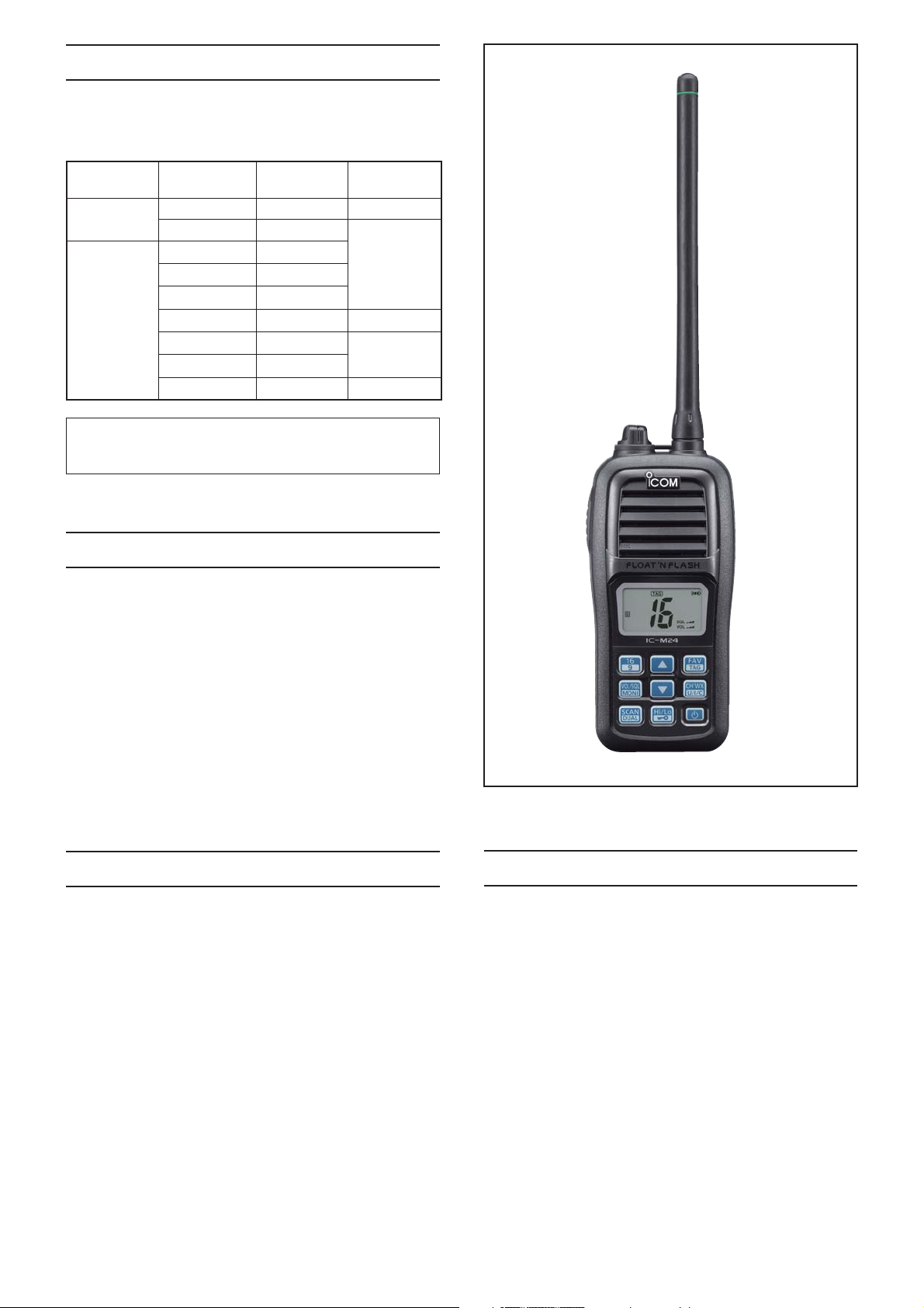
(IC-M24)
REPAIR NOTES
1. Make sure that the problem is internal before disassembling the transceiver.
2. DO NOT open the transceiver until the transceiver is
disconnected from its power source.
3. DO NOT force any of the variable components. Turn them
slowly and smoothly.
4. DO NOT short any circuits or electronic parts. An
insulated tuning tool MUST be used for all adjustments.
5. DO NOT keep power ON for a long time when the
transceiver is defective.
6. DO NOT transmit power into a Standard Signal Generator
or a Sweep Generator.
7. ALWAYS connect a 30 dB to 40 dB attenuator between
the transceiver and a Deviation Meter or Spectrum
Analyzer, when using such test equipment.
8. READ the instructions of the test equipment throughly
before connecting it to the transceiver.
Icom, Icom Inc. and the Icom logo are registered trademarks of Icom Incorporated (Japan) in Japan, the United States, the
United Kingdom, Germany, France, Spain, Russia and/or other countries.

TABLE OF CONTENTS
SECTION 1 SPECIFICATIONS
SECTION 2 INSIDE VIEWS
SECTION 3 DISASSEMBLY INSTRUCTION
SECTION 4 CIRCUIT DESCRIPITON
4-1 RECEIVER CIRCUITS. . . . . . . . . . . . . . . . . . . . . . . . . . . . . . . . . . . . . . . . . . . . . . . . . . . . . . . . 4-1
4-2 TRANSMITTER CIRCUITS . . . . . . . . . . . . . . . . . . . . . . . . . . . . . . . . . . . . . . . . . . . . . . . . . . . . 4-2
4-3 FREQUENCY SYNTHESIZER CIRCUITS . . . . . . . . . . . . . . . . . . . . . . . . . . . . . . . . . . . . . . . . 4-3
4-4 VOLTAGE DIAGRAMS. . . . . . . . . . . . . . . . . . . . . . . . . . . . . . . . . . . . . . . . . . . . . . . . . . . . . . . . 4-3
4-5 PORT ALLOCATIONS . . . . . . . . . . . . . . . . . . . . . . . . . . . . . . . . . . . . . . . . . . . . . . . . . . . . . . . . 4-4
SECTION 5 ADJUSTMENT PROCEDURES
5-1 PREPARATION . . . . . . . . . . . . . . . . . . . . . . . . . . . . . . . . . . . . . . . . . . . . . . . . . . . . . . . . . . . . . 5-1
5-2 FREQUENCY ADJUSTMENTS. . . . . . . . . . . . . . . . . . . . . . . . . . . . . . . . . . . . . . . . . . . . . . . . . 5-2
5-3 RECEIVE ADJUSTMENTS . . . . . . . . . . . . . . . . . . . . . . . . . . . . . . . . . . . . . . . . . . . . . . . . . . . . 5-3
5-3 TRANSMIT ADJUSTMENTS . . . . . . . . . . . . . . . . . . . . . . . . . . . . . . . . . . . . . . . . . . . . . . . . . . . 5-3
SECTION 6 PARTS LIST
SECTION 7 MECHANICAL PARTS
SECTION 8 BOARD LAYOUTS
SECTION 9 BLOCK DIAGRAM
SECTION 10 VOLTAGE DIAGRAM

SECTION 1. SPECIFICATIONS
M IC-M23
D GENERAL
• Frequency coverage : Transmitting 156.000–161.450 MHz
• Mode : FM (16K0G3E)
• Antenna impedance : 50 Ω (nominal)
• Power supply requirement :
• Current drain (approximately) : TX (5 W/1.0 W/0.5 W) 2.3 A/0.9 A/0.7 A
Power save 8 mA typical
• Frequency stability : ±1.5 kHz
• Operating temperature range : –15°C to +55°C
• Dimensions : 58.5 (W) × 128.5(H) × 34.5(D) mm
(Projections not included)
• Weight : Approximately 260 g
(including battery pack, antenna, belt clip)
Receiving 156.000–163.425 MHz
BP-266 only (3.7 V DC nominal; negative ground)
Maximum audio 0.35 A typical
D TRANSMITTER
• Output power : 5 W (approx.; High)/1 W (Low)/0.5 W (E_Low)*
* 1 W (High) and 0.5 W (Low) for German
• Modulation system : Variable reactance frequency modulation
• Maximum frequency deviation : ±5 kHz
• Adjacent channel power : 70 dB
• Spurious emissions : 0.25 µW
• Audio harmonic distortion : 10% (at 60% deviation)
• Residual modulation : 40 dB
• Audio frequency response :
version, depending on the pre-programmed
setting
+1 dB to –3 dB of 6 dB oct. from 300–3000 Hz
D RECEIVER
• Receive system : Double-conversion superheterodyne
• Intermediate frequency : 1st 21.7 MHz, 2nd 450 kHz
• Sensitivity (20 dB SINAD) : –4 dBµ emf typical
• Squelch sensitivity : –5 dBµ emf typical (at threshold)
• Intermodulation : 68 dB
• Hum and noise : 40 dB
• Audio frequency response :
• Spurious response : 70 dB
• Adjacent channel selectivity : 70 dB
• Audio output power (8 Ω) : 0.2 W (at 1 kHz, 10% distortion)
+1 dB to –3 dB of –6 dB oct. from 300–3000 Hz
M IC-M24
D GENERAL
• Frequency coverage : Transmitting 156.025–157.425 MHz
• Mode : FM (16K0G3E)
• Antenna impedance : 50 Ω (nominal)
• Power supply requirement :
• Current drain (approximately) : TX (5 W/1.0 W) 2.3 A/0.9 A
• Frequency stability : ±10 ppm
• Operating temperature range : –20°C to +60°C; –4°F to +140°F
• Dimensions : 58.5 (W) × 128.5(H) × 34.5(D) mm
(projections not included) 2.3
• Weight : Approximately 260 g; 9.2 oz
(including battery pack, antenna and belt clip)
Receiving 156.050–163.275 MHz
BP-266 only (3.7 V DC nominal; negative ground)
Max. audio
Power save 8 mA typical
0.35 A typical
(W) × 5.6 (H) × 1.3 (D) inch
D TRANSMITTER
• Output power : 5 W (approximately; High) and 1 W (Low)
• Modulation system : Variable reactance frequency modulation
• Maximum frequency deviation : ±5 kHz
• Adjacent channel power : 70 dB
• Spurious emissions : –68 dBc typical
• Residual modulation : 40 dB
• Audio frequency response : +1 dB to –3 dB of 6 dB oct. from 300–3000 Hz
D RECEIVER
• Receive system : Double-conversion superheterodyne
• Intermediate frequency : 1st 21.7 MHz, 2nd 450 kHz
• Sensitivity (12 dB SINAD) : 0.25 µV typical
• Squelch sensitivity : 0.35 µV typical (at threshold)
• Intermodulation : 70 dB typical
• Spurious response : 70 dB typical
• Adjacent channel selectivity : 70 dB typical
• Audio output impedance : 8 Ω
• Audio output power : 0.6 W typical (at 10% distortion)
All stated specifi cations are subject to change without notice or obligation.
1 - 1
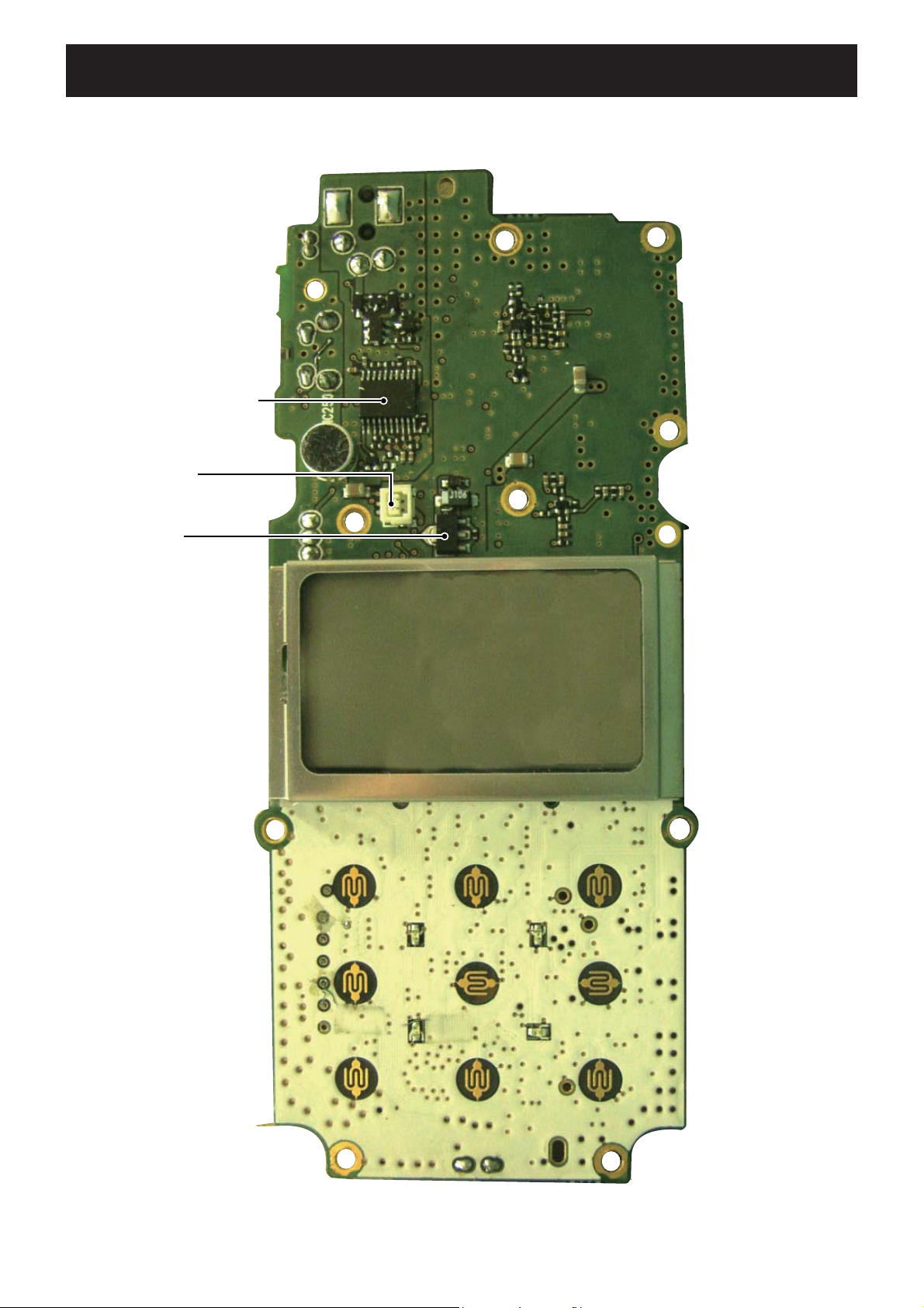
SECTION 2. INSIDE VIEWS
• MAIN UNIT
(TOP VIEW)
CHARGING CONTROLLER
SPEAKER JACK
(J251)
M3V LINE SW
(Q225)
(IC601)
2 - 1
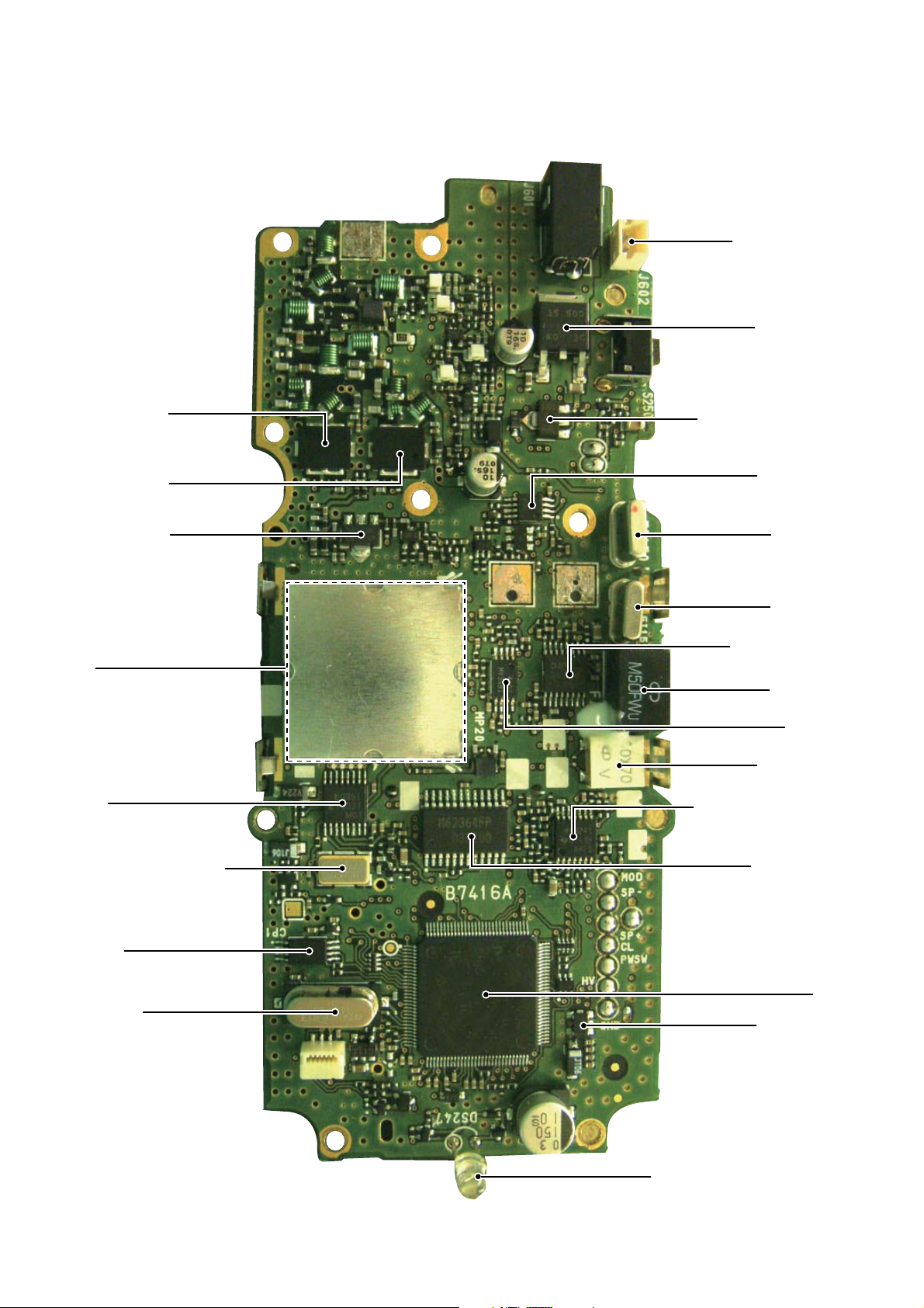
• MAIN UNIT
(BOTTOM VIEW)
WET SENSING JACK
(J602)
5 V REGULATOR
(IC602)
TX POWER AMP
(Q54)
TX POWER AMP
(Q55)
PRE-DRIVE AMP
(Q53)
VCO
PLL IC
(IC1)
CHARGING CONTROL SW
(Q602)
AF POWER AMP
(IC362)
1ST IF FILTER
(FI150)
1ST IF FILTER
(FI151)
IF DEMODULATOR IC
(IC170)
2ND IF FILTER
(FI170)
NOISE AMP
(IC365)
DISCRIMINATOR
(X170)
AF LPF/LIMIT AMP/AF AMP
(IC200)
REFERENCE FREQUENCY
OSCILLATOR
(X1)
EEPROM
(IC340)
CPU CLOCK
(X360)
D/A CONVERTER
(IC190)
CPU
(IC360)
3 V REGULATOR
(IC220)
FLASHING LED
(DS247)
2 - 2
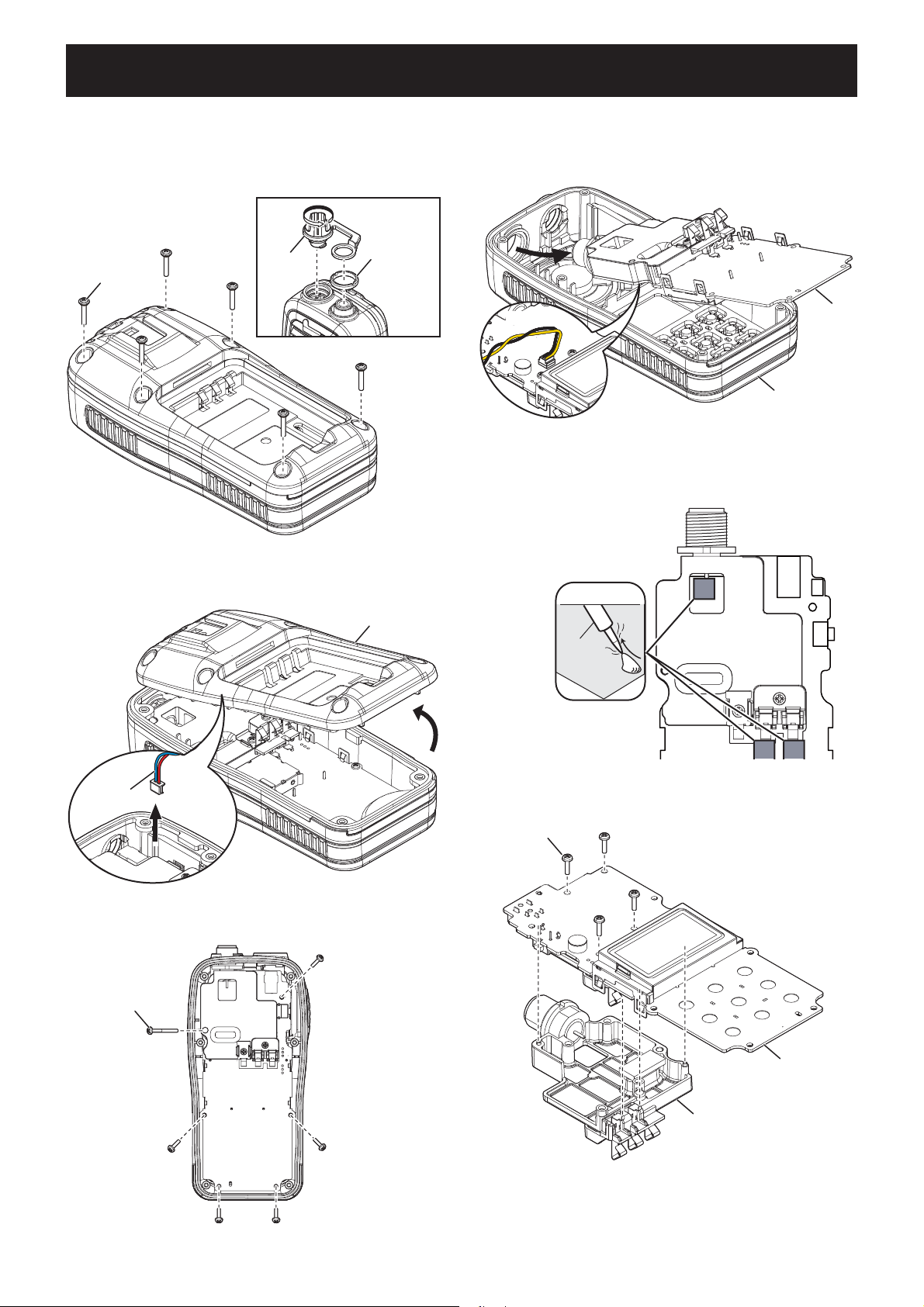
SECTION 3. DISASSEMBLY INSTRUCTION
J602J602
,J251
1. REMOVING THE PCB
1) Remove the battery pack from the transceiver.
2) Remove the DC cap and antenna nut.
3) Remove 6 screws from the rear panel.
6) CAREFULLY lift the PCB out of the front panel, and
then turn it over in order to unplug the speaker wire.
DC cap
6 screws
Antenna nut
4) CAREFULLY lift the rear panel up and unplug the
wet sensor wire.
Rear panel
SP cable
2. REMOVING THE CHASSIS
1) Unsolder 3 points shown.
UNSOLDER
Solder
remover
PCB
Front panel
Chassis
Wet sensor
wire
5) Remove 6 screws from the PCB.
6 screws
2) Remove 4 screws from the PCB, and then remove
the CHASSIS.
4 screws
PCB
Chassis
(Continued on the right above.)
3 - 1
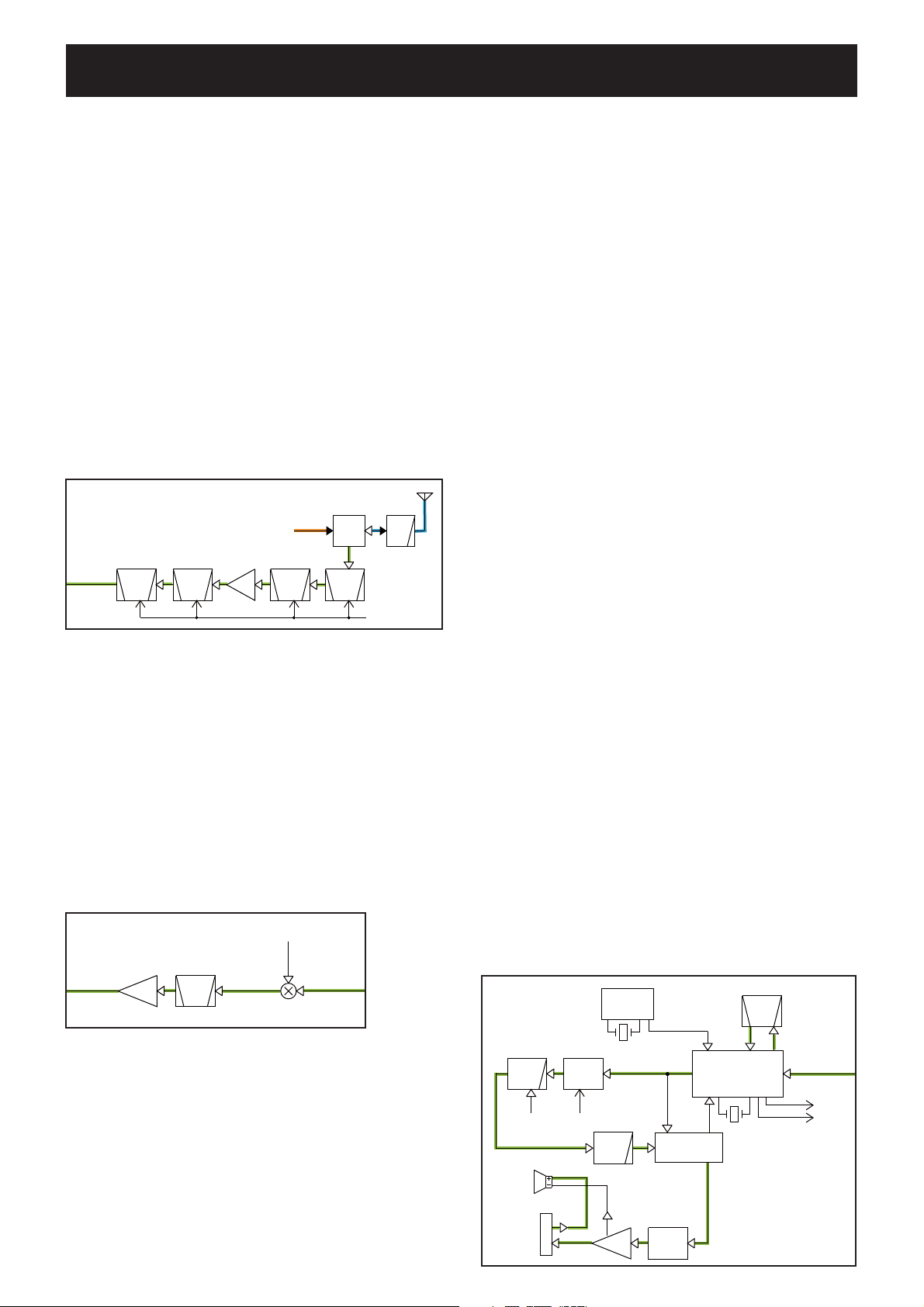
SECTION 4. CIRCUIT DESCRIPTION
4-1 RECEIVER CIRCUITS
RF CIRCUITS
The RF circuits consist of RF filters, antenna switch (ANT
SW), RF amplifi er (RF AMP), etc., and extract and amplify
the signal of frequency which is desired to receive.
• 2ND IF AND DEMODULATOR CIRCUITS
IC170 is an IF demodulate IC which contains the 2nd local
oscillator, 2nd mixer, limiter and quadrature detector in its
package.
• ANTENNA SWITCHING CIRCUIT
The RF signal from the antenna is passed through the LPF
(L81, L82, C83–C86, C89) and antenna SW (D52, D90,
L90, C90, C91), and then applied to the RF AMP (Q90)
through the 2-staged tuned BPF (D92, D93, L92, L93, C95,
C97–C100, C117).
• RF AMPLIFIER
The filtered RX signal is amplified by the RF AMP (Q90)
and passed through another 2-staged BPF (D130, D131,
L96, L97, L110, L112–L115) to remove unwanted signals.
The filtered signal is applied to the 1st mixer (Q150).
• RF CIRCUITS
ANTENNA
D52
D90
ANT
SW
D
92
LPF
T1CON
To 1st mixer
D131
BPF BPFBPF
D130
TX CIRCUITS
Q90
RF
AMP
D93
BPF
1ST IF, 2ND IF AND DEMODULATOR CIRCUITS
• 1ST IF CIRCUITS
The RX signal is mixed with 1st LO signal at the 1st
mixer (Q150), resulting in the 21.7 MHz 1st IF signal. The
converted 1st IF signal is filtered by the crystal filters (FI150
and F151) to remove unwanted out-of-band signals.
The filtered 1st IF signal is amplified by the 1st IF AMP
(Q151), and then applied to the IF demodulate IC (IC170,
pin 16).
• 1ST IF CIRCUITS
1st LO signals
from VCO
The 21.25 MHz reference frequency signal from the PLL IC
(IC1, pin 2) is applied to the IF demodulate IC (IC170, pin 2)
as the 2nd LO signal, and then mixed with 21.7 MHz 1st IF
signal from the 1st AMP (Q151). The resulting signal of 450
kHz 2nd IF signal is output from the pin 3 of IC170.
The 2nd IF signal is filtered by the external ceramic filter
(FI170) to extract 450 kHz signal only, and then applied
to the internal quadrature detector to be frequencydemodulated. The demodulated AF signals are output from
the pin 9.
The quadrature detector is a frequency demodulator which
uses a discriminator (X170) as a phase delayer, and
provides demodulation without any adjustment.
SQUELCH CIRCUIT
A portion of AF signal from the IF demodulate IC is adjusted
in level by the D/A converter (IC190), and then applied to
the noise amplifer (IC170, R174–R176, C179, C180).
Only noise components (approximately 30 kHz signal) are
amplified by the noise amplifier, and then rectified by the
internal noise detector to be converted into DC voltage
corresponding to noise level; the squelch voltage. The
squelch voltage is output from the pin 14 of IC170, and then
applied to the A/D port of the CPU (IC360, pin 33).
The CPU (IC360) compares input voltage and preset
squelch level to control audio signals ON/OFF (emit/mute).
RX AF CIRCUITS
The demodulated AF signal from the IF demodulate IC (IC170,
pin 9) is passed through the AF mute SW (IC260D) and LPF
(IC365). The filtered AF signal is de-emphasized by R286 and
C285 to obtain –6 dB/oct. of frequency response, and then
applied to the D/A converter (IC190). The level-adjusted AF
signal is amplified by the AF power amplifier (IC362), and then
applied to the speaker (CHASSIS: SP1).
To IF IC
Q151
FI151
FI150,
IF
AMP
BPF
21.7MHz
1st IF signal
From RF AMP
Q150
• 2ND IF, DEMODULATOR AND RX AF CIRCUITS
IC365
LPF
BEEP
IC1
PLL IC
21.25 MHz
2ND LO signal
X1
21.25MHz
IC260D
AF
MUTE
DETMS
R286, C285
VOLIN
SP1
LPF
De-emphasis
DET
SQLI
IC190
D/A IC
IC170
SQLO
IF IC
X170
450KHz
FI170
450KHz
BPF
RSSI
NOISE LEVEL
From 1st IF AMP
Int. SP
Ext. SP
J250
SPO
AFOUT
IC362
AF
AMP
DE ENPHA
VOL
4 - 1
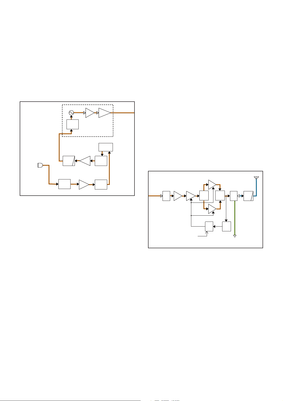
4-2 TRANSMITTER CIRCUITS
TX AF CIRCUITS
AF signal from the microphone (MIC signals) is passed
through the MIC mute SW (IC260A), amplifi ed by MIC AMP
(IC200B), and then applied to the D/A converter (IC190),
through another MIC mute SW (IC260C).
TX AMPLIFIERS
The frequency-modulated signal from the VCO (Q21, Q22,
D22) is passed through the buffers (Q23 and Q24) and LO
SW (D50), and then sequentially amplified by the buffer
AMP (Q50) and pre-drive AMP (Q53).
The level-adjusted MIC signal is pre-emphasized by R201
and C385 to obtain +6 dB/oct of frequency response, and
then passed through the limiter (IC200A) to prevent over
deviation. The amplitude-limited MIC signal is fi ltered by the
splatter fi lter (IC200D) to remove 3 kHz and higher signals,
and then applied to the VCO (Q21, Q22, D22) for frequency
modulation.
• TX AF AND MODULATION CIRCUITS
Q23
IC190
PRE
ENPHA
IC260C
MUTE
Q24
BUFFBUFF
VCO
D/A
MIC
To LO switch
MIC
MC250
INMIC
IC260A
Q 21,Q22
D22
MOD
IC200D
MIC
MUTE
LPF
MOD
MUTE
Q20
D20
D
21
IC200A
IC200B
MIC
AMP
LIMI
AMP
T
The amplifi ed signal is splitted by the power splitter (L100,
L101, R463, C445, C446) and applied to the power AMPs
(Q54 and Q55). The amplifi ed signals are combined at the
power combiner (L107, L108, R465, C457, C458) to obtain
the TX output power.
The amplified TX signal is passed through the ANT SW
(D52) and LPF, and then applied to the antenna.
APC CIRCUIT
A portion of TX output signal is rectifi ed by D91 to produce
the DC voltage which corresponds to the TX power level.
The APC AMP (IC50) compares the voltage and TX power
setting voltage from the D/A converter (IC190). The resulting
voltage from the APC AMP controls the gain of both driver
AMP (Q53) and power AMPs (Q54 and Q55), to keep the TX
output power stable.
• TX AMPLIFIERS AND APC CIRCUIT
ANTENNA
J1
LPF
From VCO
Q54
PWR
D50
Q50
Q53
BUFF
PRE
DRIVE
LO
SW
PWR
SPLITTER
AMP
PWR
AMP
Q55
PWR
COMBINER
D90
D52
ANT
SW
PCON
IC50
Q357
APC
CTRL
D91
PWR
DET
Receive circuits
4 - 2
 Loading...