


SERVICE
MANUAL
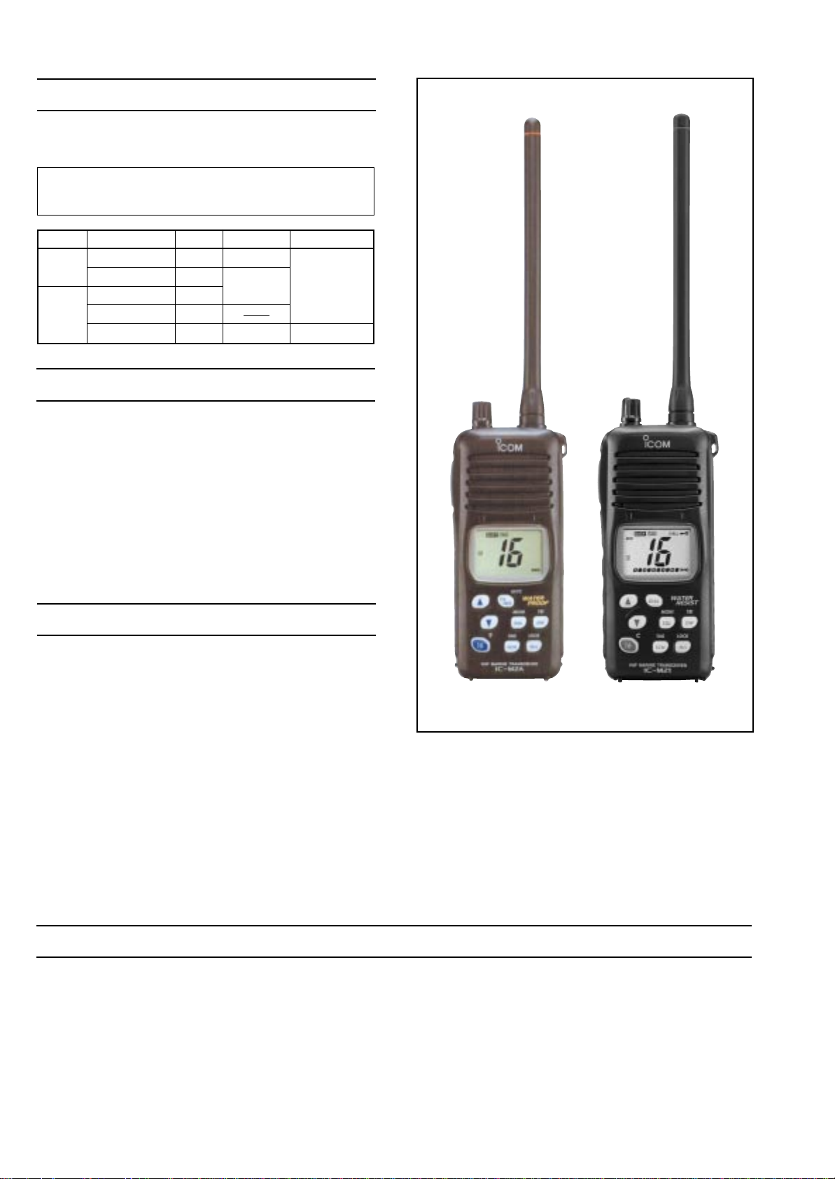
VHF MARINE TRANSCEIVER
INTRODUCTION
DANGER
ORDERING PARTS
REPAIR NOTES
This service manual describes the latest service information
for the
IC-M2A/IC-M21 VHF MARINE TRANSCEIVER
at the
time of publication.
NEVER connect the transceiver to an AC outlet or to a DC
power supply that uses more than 10 V. This will ruin the
transceiver.
DO NOT expose the transceiver to rain, snow or any liquids.
DO NOT reverse the polarities of the power supply when con-
necting the transceiver.
DO NOT apply an RF signal of more than 20 dBm (100mW)
to the antenna connector. This could damage the transceiver’s front end.
Be sure to include the following four points when ordering
replacement parts:
1. 10-digit order numbers
2. Component part number and name
3. Equipment model name and unit name
4. Quantity required
<SAMPLE ORDER>
1130007020 S.IC TC7S66FU IC-M2A MAIN UNIT 1 piece
8810004860 Screw PH M 2 x 6 ZK IC-M21 Chassis 10 pieces
Addresses are provided on the inside back cover for your
convenience.
1. Make sure a problem is internal before disassembling the transceiver.
2. DO NOT open the transceiver until the transceiver is disconnected from its power source.
3. DO NOT force any of the variable components. Turn them slowly and smoothly.
4. DO NOT short any circuits or electronic parts. An insulated turning tool MUST be used for all adjustments.
5. DO NOT keep power ON for a long time when the transceiver is defective.
6. DO NOT transmit power into a signal generator or a sweep generator.
7. ALWAYS connect a 40 dB to 50 dB attenuator between the transceiver and a deviation meter or spectrum analyzer when
using such test equipment.
8. READ the instructions of test equipment thoroughly before connecting equipment to the transceiver.
To upgrade quality, all electrical or mechanical parts and
internal circuits are subject to change without notice or obligation.
IC-M2A IC-M21
Model
IC-M2A
IC-M21
Version
U.S.A.
S.E.Asia
Europe
United Kingdom
Germany
Symbol
[USA]
[SEA]
[EUR]
[UK]
[FRG]
AC adapter
BC-147A
BC-147E
BC-147E
TX high power
5W
1W

TABLE OF CONTENTS
SECTION 1 SPECIFICATIONS
SECTION 2 INSIDE VIEWS
SECTION 3 DISASSEMBLY INSTRUCTIONS
SECTION 4 CIRCUIT DESCRIPTION
4-1 RECEIVER CIRCUITS . . . . . . . . . . . . . . . . . . . . . . . . . . . . . . . . . . . . . . . . . . . . . . . . . . . . .4-1
4-2 TRANSMITTER CIRCUITS . . . . . . . . . . . . . . . . . . . . . . . . . . . . . . . . . . . . . . . . . . . . . . . . .4-2
4-3 PLL CIRCUIT . . . . . . . . . . . . . . . . . . . . . . . . . . . . . . . . . . . . . . . . . . . . . . . . . . . . . . . . . . . .4-3
4-4 POWER SUPPLY CIRCUITS . . . . . . . . . . . . . . . . . . . . . . . . . . . . . . . . . . . . . . . . . . . . . . . .4-3
4-5 CPU PORT ALLOCATIONS . . . . . . . . . . . . . . . . . . . . . . . . . . . . . . . . . . . . . . . . . . . . . . . . .4-4
SECTION 5 ADJUSTMENT PROCEDURES
5-1 PREPARATION . . . . . . . . . . . . . . . . . . . . . . . . . . . . . . . . . . . . . . . . . . . . . . . . . . . . . . . . . .5-1
5-2 PLL AND TRANSMITTER ADJUSTMENTS . . . . . . . . . . . . . . . . . . . . . . . . . . . . . . . . . . . . .5-4
5-3 RECEIVER ADJUSTMENT . . . . . . . . . . . . . . . . . . . . . . . . . . . . . . . . . . . . . . . . . . . . . . . . . .5-5
SECTION 6 PARTS LIST
SECTION 7 MECHANICAL PARTS AND DISASSEMBLY
SECTION 8 SEMI-CONDUCTOR INFORMATION
SECTION 9 BOARD LAYOUTS
9-1 CHARGE UNIT (BC-150) . . . . . . . . . . . . . . . . . . . . . . . . . . . . . . . . . . . . . . . . . . . . . . . . . . .9-1
9-2 MAIN UNIT . . . . . . . . . . . . . . . . . . . . . . . . . . . . . . . . . . . . . . . . . . . . . . . . . . . . . . . . . . . . .9-2
9-3 VR UNIT . . . . . . . . . . . . . . . . . . . . . . . . . . . . . . . . . . . . . . . . . . . . . . . . . . . . . . . . . . . . . . .9-4
SECTION 10 BLOCK DIAGRAM
SECTION 11 VOLTAGE DIAGRAM
11-1 MAIN UNIT . . . . . . . . . . . . . . . . . . . . . . . . . . . . . . . . . . . . . . . . . . . . . . . . . . . . . . . . . . . . .11-1
11-2 VR UNIT . . . . . . . . . . . . . . . . . . . . . . . . . . . . . . . . . . . . . . . . . . . . . . . . . . . . . . . . . . . . . . .11-2

1 - 1
All stated specifications are subject to change without notice or obligation.
Frequencycoverage
Mode
Power supply requirement
Usable temperature
Frequency stability
at 5 W
at 3 W
at 1 W
at 0.5 W
at maximum audio
at stand-by
Antenna impedance
Dimensions
(Projections not included)
Weight
(with antenna and BP-224)
RF output power (at 7.2 V DC)
Modulation system
Max. frequency deviation
Frequency error
Spurious emissions
Adjacent channel power
Residual modulation
Audio harmonic distortion
Audio frequency response
Microphone impedance
Receive system
Intermediate frequencies
Sensitivity
Squelch sensitivity
Adjacent channel selectivity
Spurious response
Intermodulation
Hum and noise
Audio output power ( at 7.4 V)
Audio frequency response
IC-M2A IC-M21
RECEIVER TRANSMITTER GENERAL
Tx: 156.025 MHz–157.425 MHz Tx: 156.000 MHz–161.450 MHz
Rx: 156.025 MHz–163.275 MHz Rx: 156.000 MHz–163.425 MHz
16K0G3E (FM)
BP-224 (7.2 V DC)
–20 ˚C to +60 ˚C (–4˚F to +140˚F) –15 ˚C to +55 ˚C (+5˚F to +131˚F)
± 10 ppm ± 1.5 kHz
1.5 A
1.2 A
0.7 A
0.6 A [FRG] only
200 mA
20 mA
Type STUD / 50 Ω
61(W)
× 135H) × 41(D) mm; 213⁄32(W) × 55⁄16(H) × 15⁄8(D) inch (with BP-224)
360 g; 12.7 oz (approx.)
Hi power; 5 W 5 W / 3 W / 1 W (High / Mid / Low) [OTHER]
Hi power; 1 W 1 W / 0.5 W (High / Low) [FRG]
Variable reactance frequency modulation
± 5.0 kHz
± 10 ppm ± 1.5 kHz
–65 dBc 250 nW
60 dB 70 dB
40 dB
Less than 10 % at 60 % deviation
+ 1 kHz to –3 dB of 6 dB octave from 300 Hz to 3000 Hz
2 kΩ
Double-conversion super heterodyne
1st: 21.70 MHz, 2nd: 450 kHz
0.25 µV at 12 dB SINAD 0.79 µV emf at 12 dB SINAD (typical)
0.35 µV 1.0 µV emf (typical)
70 dB (typical) 70 dB
70 dB (typical) 70 dB
70 dB (typical) 68 dB
40 dB
350 mW typical at 10 % distortion 200 mW at 10 % distortion
with an 8 Ω load with an 8 Ω load
–3 dB to +1 dB of –6 dB octave from 300 Hz to 3000 Hz
Current drain
(with BP-224)
Tx
Rx
SECTION 1 SPECIFICATIONS
Measurements made in accordance with TIA/EIA-603 or EN-301-178-2.

1 - 2
* Low power only
NOTE: Channels 3, 21, 23, 61, 64, 81, 82 and 83 CANNOT be used by the general public in USA waters.
CAN
21A
22A
23
24
25
26
27
28
60
61A
62A
64
64A
65A
66A*
67
68
69
70
71
72
CAN
73
74
77*
78A
79A
80A
81A
82A
83
83A
84
85
86
87
88
21b
25b
28b
83b
CAN
01
02
03
04A
05A
06
07A
08
09
10
11
12
13*
14
15*
16
17*
18A
19A
20*
21
‘‘
VHF MARINE CHANNEL LIST (For IC-M2A)
USA
01A
03A
05A
06
07A
08
09
10
11
12
13*
14
15*
16
17*
18A
19A
20
20A
INT
01
02
03
04
05
06
07
08
09
10
11
12
13
14
15*
16
17
18
19
20
21
Transmit
156.050
156.050
156.100
156.150
156.150
156.200
156.200
156.250
156.250
156.300
156.350
156.350
156.400
156.450
156.500
156.550
156.600
156.650
156.700
156.750
156.800
156.850
156.900
156.900
156.950
156.950
157.000
157.000
157.050
Receive
160.650
156.050
160.700
160.750
156.150
160.800
156.200
160.850
156.250
156.300
160.950
156.350
156.400
156.450
156.500
156.550
156.600
156.650
156.700
156.750
156.800
156.850
161.500
156.900
161.550
156.950
161.600
157.000
161.650
USA
21A
22A
23A
24
25
26
27
28
61A
63A
64A
65A
66A
67*
68
69
70
71
72
INT
22
23
24
25
26
27
28
60
61
62
63
64
65
65A
66
66A
67
68
69
70
71
72
Transmit
157.050
157.100
157.100
157.150
157.150
157.200
157.250
157.300
157.350
157.400
156.025
156.075
156.075
156.125
156.125
156.175
156.175
156.225
156.225
156.275
156.275
156.325
156.325
156.375
156.425
156.475
Rx only
156.575
156.625
Receive
157.050
161.700
157.100
161.750
157.150
161.800
161.850
161.900
161.950
162.000
160.625
160.675
156.075
160.725
156.125
160.775
156.175
160.825
156.225
160.875
156.275
160.925
156.325
156.375
156.425
156.475
156.525
156.575
156.625
USA
73
74
77*
78A
79A
80A
81A
82A
83A
84
84A
85
85A
86
86A
87
87A
88
88A
INT
73
74
77
78
79
80
81
82
83
84
85
86
87
88
Transmit
156.675
156.725
156.875
156.925
156.925
156.975
156.975
157.025
157.025
157.075
157.075
157.125
157.125
157.175
157.175
157.225
157.225
157.275
157.275
157.325
157.325
157.375
157.375
157.425
157.425
Rx only
Rx only
Rx only
Rx only
Receive
156.675
156.725
156.875
161.525
156.925
161.575
156.975
161.625
157.025
161.675
157.075
161.725
157.125
161.775
157.175
161.825
157.225
161.875
157.275
161.925
157.325
161.975
157.375
162.025
157.425
161.650
161.850
162.000
161.775
Channel No. Frequency (MHz) Channel No. Frequency (MHz) Channel No. Frequency (MHz)
WX01
WX02
WX03
WX04
WX05
Transmit
Receive only
Receive only
Receive only
Receive only
Receive only
Receive
162.550
162.400
162.475
162.425
162.450
WX06
WX07
WX08
WX09
WX10
Transmit
Receive only
Receive only
Receive only
Receive only
Receive only
Receive
162.500
162.525
161.650
161.775
163.275
Frequency (MHz) Frequency (MHz)
Weather
channel
Weather
channel
‘‘
WX CHANNEL LIST ([IC-M2A] only)

1 - 3
* Low power only
‘‘
VHF MARINE CHANNEL LIST (For IC-M21)
USA
01A
03A
05A
06
07A
08
09
10
11
12
13*
14
15*
16
17*
18A
19A
20
20A
21A
INT
01
02
03
04
05
06
07
08
09
10
11
12
13
14
15*
16
17
18
19
20
21
Transmit
156.050
156.050
156.100
156.150
156.150
156.200
156.250
156.250
156.300
156.350
156.350
156.400
156.450
156.500
156.550
156.600
156.650
156.700
156.750
156.800
156.850
156.900
156.900
156.950
156.950
157.000
157.000
157.050
157.050
Receive
160.650
156.050
160.700
160.750
156.150
160.800
160.850
156.250
156.300
160.950
156.350
156.400
156.450
156.500
156.550
156.600
156.650
156.700
156.750
156.800
156.850
161.500
156.900
161.550
156.950
161.600
157.000
161.650
157.050
USA
22A
23A
24
25
26
27
28
37A
61A
63A
64A
65A
66A
67*
68
69
70
71
72
73
INT
22
23
24
25
26
27
28
60
61
62
63
64
65
65A
66
66A
67
68
69
70
71
72
73
Transmit
157.100
157.100
157.150
157.150
157.200
157.250
157.300
157.350
157.400
157.850
156.025
156.075
156.075
156.125
156.175
156.175
156.225
156.225
156.275
156.275
156.325
156.325
156.375
156.425
156.475
Rx only
156.575
156.625
156.675
Receive
161.700
157.100
161.750
157.150
161.800
161.850
161.900
161.950
162.000
157.850
160.625
160.675
156.075
160.725
160.775
156.175
160.825
156.225
160.875
156.275
160.925
156.325
156.375
156.425
156.475
156.525
156.575
156.625
156.675
USA
74
77*
78A
79A
80A
81A
82A
83A
84
84A
85
85A
86
86A
87
87A
88
88A
INT
74
77
78
79
80
81
82
83
84
85
86
87
88
Transmit
156.725
156.875
156.925
156.925
156.975
156.975
157.025
157.025
157.075
157.075
157.125
157.125
157.175
157.175
157.225
157.225
157.275
157.275
157.325
157.325
157.375
157.375
157.425
157.425
Receive
156.725
156.875
161.525
156.925
161.575
156.975
161.625
157.025
161.675
157.075
161.725
157.125
161.775
157.175
161.825
157.225
161.875
157.275
161.925
157.325
161.975
157.375
162.025
157.425
Channel No. Frequency (MHz) Channel No. Frequency (MHz) Channel No. Frequency (MHz)

2 - 1
SECTION 2 INSIDE VIEWS
• MAIN UNIT
TOP VIEW BOTTOM VIEW
Antenna switching circuit
(D52: 1SV307)
Power amplifier
(Q54: 2SK2974)
APC
(IC50: NJM2125F)
IF amplifier
(Q151: 2SC2714 Y)
TX/RX switch
(D50, D51: MA77)
Antenna switching circuit
D90: 1SV307
D91: 1SS375
()
1st mixer
(Q150: 3SK272)
VCO circuit
IF DETECTOR IC
(IC170: TA31136FN)
PLL IC
(IC1: µPD3140GS)
D/A converter
(IC190: M62363FP-650C)
CPU
(IC360: HD6433844RA60H)
EEPROM
(IC340: HN58X2416TI)
Mic amplifier and
low pass filter circuits
(IC200: NJM2902V)

MAIN unit
Chassis
Earth plate
H
H
H
I
I
H
I
I
3 - 1
SECTION 3 DISASSEMBLY INSTRUCTIONS
• Removing the Rear panel
• Removing the Chassis unit
Rear panel
A
B
C
C
Rubber
Front panel
Front panel
Chassis unit
VR unit
E
G
D
F (Speaker connector)
¡ Unscrew 1 screw, A (2 x 10 mm), and remove 1 washer, B.
™ Unscrew 3 screws, C (2 x 8 mm).
£ Remove the rear panel and rubber from the front panel.
¡ Unscrew 1 nut, D.
™ Unscrew 2 screws, E (2 x 6 mm).
£ Take off the chassis unit in the direction of the arrow.
¢ Unplug, F, to separate the front panel, J251, and the
chassis unit.
∞ Remove 1 washer, G.
• Removing the MAIN unit
¡ Unscrew 9 screws, H (2 x 4 mm).
™ Unsolder 4 points, I, and remove earth plate.
£ Separate the MAIN unit and the chassis.

4 - 1
4-1 RECEIVER CIRCUITS
4-1-1 ANTENNA SWITCHING CIRCUIT
(MAIN UNIT)
The antenna switching circuit functions as a low-pass filter
while receiving and as resonator circuit while transmitting.
The circuit does not allow transmit signals to enter receiver
circuits.
Received signals from the antenna connector pass through
the low-pass fileter (L80–L82, C80–C86) and antenna
switching circuit (D52, D90, D91). The filtered signals are
then applied to the RF amplifier circuit (Q90).
4-1-2 RF AND 1ST MIXER CIRCUITS (MAIN UNIT)
The 1st mixer circuit converts the received signals to a fixed
frequency of the 1st IF signal with a PLL output frequency.
By changing the PLL frequency, only the desired frequency
will be passed through a pair of crystal filters at the next
stage of the 1st mixer.
The signals from the antenna switching circuit are passed
through the tunable bandpass filter (D92, D93) and amplified
at the RF amplifier (Q90). The amplified signals are passed
through another tunable bandpass fileter (D130), and then
applied to the 1st mixer circuit (Q150).
The filtered signals are mixed at the 1st mixer (Q150) with a
1st LO signal coming from the PLL circuit to produce a 21.7
MHz 1st IF signal. The 1st IF signal is passed through two
crystal filters (FI150, FI151) and is then amplified at the IF
amplifier (Q151).
4-1-3 2ND IF AND DEMODULATOR CIRCUITS
(MAIN UNIT)
The 2nd mixer circuit converts the 1st IF signal to a 2nd IF
signal. Adouble convertion superheterodyne system (which
converts receive signal twice) improves the image rejection
and obtain stable receiver gain.
The 1st IF signal is applied to a 2nd mixer section of the FM
IF IC (IC170, pin 16). The signal is then mixed with a 2nd LO
signal for conversion into a 450 kHz 2nd IF signal.
IC170 contains the 2nd mixer, limiter amplifier, quadrature
detector and active filter circuits. A21.25 MHz 2nd LO signal
is produced at the PLL circuit using the reference frequency.
The 2nd IF signal from the 2nd mixer (IC170, pin 3) passes
through ceramic filters (FI170) to remove unwanted heterodyned frequencies. It is then amplified at the limiter amplifier section (IC170, pin 5) and applied to the quadrature
detector section (IC170, pins 10 and 11) to demodulate the
2nd IF signal into AF signals.
4-1-4 AF CIRCUIT (MAIN UNIT)
AF signals from the FM IF IC (IC170, pin 9) are fed to the
analog switch (IC260).
The AF signals (detected signals) are passed through the
analog switch (IC260, pins 2 and 1) and are then applied to
the active low-pass filter (IC200c, pin 9).
The filtered AF signals are applied to and adjusted audio
level at the [VOL] control (VR unit; R500). The level controlled signals are passed through the AF mute switch
(Q280) which is controlled by “IVOLM” signal from the CPU
(IC9, pin 31). The passed signals are applied to the AF
power amplifier (IC280, pin 4), and then output to the internal speaker or [EXT SP] jack after being passed through the
de-emphasis circuit (R286, C285) to obtain the –6 dB/octave
frequency characteristics.
Mixer
16
IF amp.
2nd IF filter
450 kHz
PLL IC
IC1
X1
21.25 MHz
RSSI
IC170 TA31136FN(D)
14
"IF" (1st IF signal: 21.7 MHz)
from Q151
"RSSIV" signal to the CPU (pin 94)
11
10
9
87 5 3
2
17
16
Active
filter
FI170
Noise
detector
FM
detector
Noise
comp.
"NOISV" signal to the CPU (pin 90)
12
C171
C174
R172
C176
C175
C180
C179
"SQLO" signal to the D/A
convertor IC (IC190, pin 15)
"SQLI" signal to the D/A
convertor IC (IC190, pin 16)
R175
R176
R174
AF signal "DET"
2nd
R171
X170
450 kHz
R5V
R170
SECTION 4 CIRCUIT DESCRIPTION
• 2ND IF AND DEMODULATOR CIRCUITS

4 - 2
4-1-5 SQUELCH CIRCUIT (MAIN UNIT)
The noise squelch circuit cuts out AF signals when no RF
signals are received. By detecting noise components in the
AF signals, the squelch circuit switches the AF mute switch.
A portion of the AF signals divided by C175 from the FM IF
IC (IC170, pin 9) are applied to the D/Aconvertor (IC190, pin
16) to adjust amplitude. The signals from the D/A convertor
(IC190, pin 15) are applied to the active filter section (IC170,
pin 8). The active filter section amplifies and filters noise
components. The filtered signals are applied to the noise
detector section and output from IC170 (pin 14) as the
“NOISV” signal.
The “NOISV” signal from IC170 (pin 14) is applied to the
CPU (IC360, pin 90). The CPU compares the set squelch
level voltage and “NOISV” signal voltage to control the
squelch output.
4-2 TRANSMITTER CIRCUITS
4-2-1 MICROPHONE AMPLIFIER CIRCUIT
(MAIN UNIT)
The microphone amplifier circuit amplifies audio signals with
+6 dB/octave pre-emphasis characteristics from the microphone to a level needed for the modulation circuit.
The AF signals from the microphone are passed through the
pre-emphasis circuit (R253, C254) and are then applied to
the microphone amplifier (IC200b). The amplified AF signals
are applied to analog switch (IC260, pin 5).
The AF signals are amplified again at the limiter-amplifier
(IC200a) and then passed through the low-pass filter
(IC200d, pins 10 and 8). The filtered audio is applied to the
modulation circuit as the “MOD” signal.
4-2-2 MODULATION CIRCUIT (MAIN UNIT)
The modulation circuit modulates the VCO oscillating signal
(RF signal) using the microphone audio signals.
The audio signals “MOD” change the reactance of D22 and
D23 to modulate an oscillated signal at the VCO circuit
(Q21, Q22, D22, D23). The oscillated signal is amplified at
the buffer-amplifiers (Q23, Q24).
4-2-3 DRIVE/POWER AMPLIFIER CIRCUITS
(MAIN UNIT)
The signal from the VCO circuit passes through the transmit/receive switching circuit (D50, D51) and is applied to the
buffer-amplifier (Q50). The amplified signal is amplified by
the pre-driver (Q53) and the power amplifier (Q54) to obtain
5 W of RF power (at 7.2 V). The amplified signal passes
through the antenna switching circuit (D52), and low-pass filter (L80–L82, C80–C86) and is then applied to the antenna
connector.
The bias current of the pre-driver (Q53) and the power
amplifier (Q54) is controlled by the APC circuit to stabilize
the output power.
4-2-4 APC CIRCUIT (MAIN UNIT)
The APC (Automatic Power Control) circuit provides stable
output power from the power amplifier even when the input
voltage or temperature changes, and selects HIGH, MIDDLE or LOW (1W type selects HIGH or LOW) output power.
The APC circuit consists of a power detector and APC control circuits.
• POWER DETECTOR CIRCUIT (MAIN UNIT)
The power detector circuit (D80, C87) detects the transmit
output power level and converts it to DC voltage as the
“TDETV” signal. The detected signal is applied to the APC
control circuit.
• APC CONTROL CIRCUIT (MAIN UNIT)
The “TDETV” signal from the power detector circuit is
applied to the CPU (IC360, pin 92) to control the input voltage of the pre-driver (Q53) and the power amplifier (Q54).
When the output power changes, the CPU (IC360) outputs
APC control signal to the D/A converter (IC190). And then
“PCON” signal from the D/Aconverter controls the APC controller (IC50) to provide stable output power.
I. SENS
Q53
IC50
Q51, Q52
APC ctrl
To the 1st IF circuit
PWR amp.
Pre-Drive
D80, C87
Q54
D52
D91
Ant SW
Ant
D90
+
"PCON" signal
from IC190 (pin 3)
"TDETV" signal
to CPU (pin 92)
The amplified signal from the
buffer amplifier (Q50)
"VCC"
"T5V"
PWR det.
TX
RX
• APC CIRCUIT

4 - 3
4-3 PLL CIRCUIT (RF UNIT)
A PLL circuit provides stable oscillation of the transmit frequency and receive 1st LO frequency. The PLL output compares the phase of the divided VCO frequency to the reference frequency. The PLL output frequency is controlled by
the divided ratio (N-data) of a programmable divider.
The PLL circuit contains a VCO (Q21, Q22, D22, D23). The
oscillated signal is amplified at the buffer-amplifiers (Q23,
Q25) and then applied to the PLL IC (IC1, pin 19).
The PLL IC contains the prescalers, programmable counter,
programmable divider, phase selector and etc. The entered
signal is divided at the prescaler and programmable counter
sections by the N-data ratio from the CPU. The divided signal is detected on phase at the phase detector using the reference frequency.
If the oscillated signal drifts, the phase of its frequency
changes from the reference frequency, causing a lock voltage changes to compensate for the drift in the oscillated frequency.
A portion of the VCO signal is amplified at buffer-amplifiers
(Q23, Q24) and is then applied to the receive 1st mixer
(Q150) or transmit buffer amplifier (Q50) via the TX/RX
switching diode (D50, D51).
Shift register
Prescaler
Phase
detector
Loop
filter
Programmable
counter
Programmable
divider
X1
21.25 MHz
"2nd LO" signal (21.25 MHz)
to the FM IF IC (IC170)
Q21, Q22, D22, D23
VCO
Buffer
Buffer
Buffer
Q24
D50
D51
Q25
Q23
3
4
5
PLST
IC1 (PLL IC)
SCK
SO
to transmitter circuit
to the 1st mixer circuit
17
16
13
19
LINE
HV
VCC
CPU5V
5V
R5V
V5V
T5V
DESCRIPTION
The voltage from the attached battery pack.
The same voltage as the HV line (battery volt-
age) which is controlled by the power switch (RF
unit; [OFF/VOL] control).
Common 5 V converted from the VCC line by the
CPU5V regulator circuit (IC220).
The output voltage is applied to the CPU (MAIN
unit; IC360), REG5V regulator, etc.
Common 5V converted from the VCC line by the
5V regulator circuit (Q223–Q225).
The output voltage is applied to the D/A converter (IC190) and PLL IC (IC1), etc.
Receive 5V converted from the 5V line by the R5
regulator circuit (Q221).
The regulated voltage is applied to the MOD
MUTE circuit (Q20, D20, D21) and receiver circuit.
Common 5V converted from the 5V line by the
V5 regulator circuit (Q220).
The regulated voltage is applied to the VCO circuit
Transmit 5V converted from the 5V line by the T5
regulator circuit (Q222).
The regulated voltage is applied to the transmitter circuit.
4-4 POWER SUPPLY CIRCUITS
VOLTAGE LINES
• PLL CIRCUIT
 Loading...