

Page 1

SERVICE
MANUAL
SURVIVAL CRAFT 2-WAY RADIO
Page 2
INTRODUCTION
This service manual describes the latest service information
for the
time of publication.
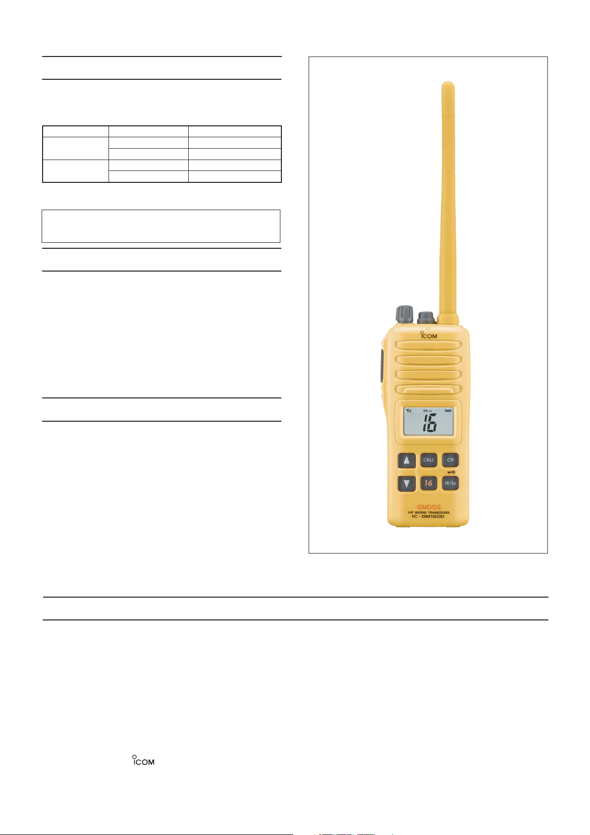
IC-GM1600/E VHF MARINE TRANSCEIVER
MODEL VERSION TX Hi-POWER
IC–GM1600
IC–GM1600E
To upgrade quality, all electrical or mechanical parts and
internal circuits are subject to change without notice or
obligation.
USA 2 W
GEN 2 W
EUR 2 W
UK 2 W
at the
DANGER
NEVER connect the transceiver to an AC outlet or to a DC
power supply that uses more than 7.5 V. Such a connection
could cause a fire or electric hazard.
DO NOT reverse the polarities of the power supply when
connecting the transceiver.
DO NOT apply an RF signal of more than 20 dBm (100 mW)
to the antenna connector. This could damage the transceiver's front end.
ORDERING PARTS
Be sure to include the following four points when ordering
replacement parts:
1. 10-digit order numbers
2. Component part number and name
3. Equipment model name and unit name
4. Quantity required
<SAMPLE ORDER>
5030002790 LCD A0286 IC-GM1600 Main unit 5 pieces
8810009510 Screw BO 2x4 NIxZU (BT) IC-GM1600E Chassis 10 pieces
Addresses are provided on the inside back cover for your
convenience.
REPAIR NOTES
1. Make sure a problem is internal before disassembling the transceiver.
2. DO NOT open the transceiver until the transceiver is disconnected from its power source.
3. DO NOT force any of the variable components. Turn them slowly and smoothly.
4. DO NOT short any circuits or electronic parts. An insulated turning tool MUST be used for all adjustments.
5. DO NOT keep power ON for a long time when the transceiver is defective.
6. DO NOT transmit power into a signal generator or a sweep generator.
7. ALWAYS connect a 30 dB to 40 dB attenuator between the transceiver and a deviation meter or spectrum analyzer when
using such test equipment.
8. READ the instructions of test equipment thoroughly before connecting equipment to the transceiver.
Icom, Icom Inc. and logo are registered trademarks of Icom Incorporated (Japan) in the United States, the United
Kingdom, Germany, France, Spain, Russia and/or other countries.
Page 3

TABLE OF CONTENTS
SECTION 1 SPECIFICATIONS
SECTION 2 INSIDE VIEWS
SECTION 3 DISASSEMBLY INSTRUCTIONS
SECTION 4 CIRCUIT DESCRIPITON
4-1 RECEIVER CIRCUITS. . . . . . . . . . . . . . . . . . . . . . . . . . . . . . . . . . . . . . . . . . . . . . . . . . . . . . . . 4-1
4-2 TRANSMITER CIRCUITS . . . . . . . . . . . . . . . . . . . . . . . . . . . . . . . . . . . . . . . . . . . . . . . . . . . . . 4-2
4-3 PLL CIRCUITS . . . . . . . . . . . . . . . . . . . . . . . . . . . . . . . . . . . . . . . . . . . . . . . . . . . . . . . . . . . . . 4-3
4-4 POWER SUPPLY CIRCUITS. . . . . . . . . . . . . . . . . . . . . . . . . . . . . . . . . . . . . . . . . . . . . . . . . . . 4-4
4-5 PORT ALLOCATIONS . . . . . . . . . . . . . . . . . . . . . . . . . . . . . . . . . . . . . . . . . . . . . . . . . . . . . . . . 4-4
SECTION 5 ADJUSTMENT PROCEDURES
5-1 PREPARATION . . . . . . . . . . . . . . . . . . . . . . . . . . . . . . . . . . . . . . . . . . . . . . . . . . . . . . . . . . . . . 5-1
5-2 SOFTWARE ADJUSTMENTS . . . . . . . . . . . . . . . . . . . . . . . . . . . . . . . . . . . . . . . . . . . . . . . . . . 5-4
SECTION 6 PARTS LIST
SECTION 7 MECHANICAL PARTS AND DISASSEMBLY
SECTION 8 SEMICONDUCTOR INFORMATION
SECTION 9 BOARD LAYOUTS
9-1 MAIN UNIT . . . . . . . . . . . . . . . . . . . . . . . . . . . . . . . . . . . . . . . . . . . . . . . . . . . . . . . . . . . . . . . . 9-1
9-2 VR BOARD . . . . . . . . . . . . . . . . . . . . . . . . . . . . . . . . . . . . . . . . . . . . . . . . . . . . . . . . . . . . . . . . 9-3
9-3 MIC BOARD. . . . . . . . . . . . . . . . . . . . . . . . . . . . . . . . . . . . . . . . . . . . . . . . . . . . . . . . . . . . . . . . 9-3
9-4 BC-158. . . . . . . . . . . . . . . . . . . . . . . . . . . . . . . . . . . . . . . . . . . . . . . . . . . . . . . . . . . . . . . . . . . . 9-3
SECTION 10 BLOCK DIAGRAM
SECTION 11 VOLTAGE DIAGRAM
11-1 MAIN UNIT . . . . . . . . . . . . . . . . . . . . . . . . . . . . . . . . . . . . . . . . . . . . . . . . . . . . . . . . . . . . . . . . 11-1
11-2 VR / MIC BOARD . . . . . . . . . . . . . . . . . . . . . . . . . . . . . . . . . . . . . . . . . . . . . . . . . . . . . . . . . . . 11-3
Page 4

SECTION 1 SPECIFICATIONS
IC-GM1600 IC-GM1600/E
[USA] [GEN], [EUR], [UK]
TX
• Frequency coverage
• Number of programable channels 100 channels
• Type of emission 16K0G3E 16K0G3E (for ATIS)
• Antenna impedance 50 Ω (nominal)
• Operating temperature range −4˚F to +140˚F –20˚C to +55˚C
• Power supply requirement 7.5 V DC nominal (negative ground) 7.2 V DC nominal (negative ground)
GENERAL
• Current drain (approx.)
• Dimensions (projections not included) 65(W) × 145(H) × 44(D) mm; 2
• Weight (approx.) 385 g; 13.58 oz. (Including BP-234)
• Output power High 2 W
• Modulation Variable reactance frequency modulation
• Max. frequency deviation ± 5.0 kHz
• Frequency error
• Spurious emissions –70 dBc typ.
• Adjacent channel power 70 dB
• Audio harmonic distortion 10% (at 60% deviation)
• FM hum and noise 40 dB –
TRANSMITTER
• Residual modulation – 40 dB
• Audio frequency response +1 dB to –3 dB of 6 dB oct. from 300 Hz to 3000 Hz
• Limiting charact. of modulation 60–100% of max. deviation
• Microphone impedance 2 k
• Receive system
• Intermediate frequencies 1st : 31.05 MHz, 2nd : 450 kHz
• Sensitivity 0.25 µV typ. at 12 dB SINAD –2 dBµ emf typ. at 20 dB SINAD
• Squelch sensitivity –6dBµ typ. (at threshold) –2 dBµ emf typ. (at threshold)
• Adjacent channel selectivity 70 dB typ. 70 dB
• Spurious response
• Intermodulation rejection ratio 70 dB typ. 68 dB
• Hum and Noise
RECEIVER
• Audio frequency response
• Audio output power
(at 10% distortion with an 8 Ω load)
• Output impedance (audio) 8
Specifications are measured in accordance with TIA/EIA–603 and FCC PARTS 80.271 (IC-GM1600),
All stated specifications are subject to change without notice or obligation.
RX 156.050–163.275 MHz [ON-BOARD] 156.000–163.425 MHz [ON-BOARD]
TX/RX 156.300–156.875 MHz [SURVIVAL]
RX 0.2 A (at max. audio)
TX
Low 1 W
156.025–157.425 MHz [ON-BOARD] 156.000–161.450 MHz [ON-BOARD]
2 W 1.0 A
1 W 0.7 A
9
/16(W) × 5 23/32(H) × 1 3/4(D) in.
±5.0 ppm ±1.5 kHz
0.25 µW (30 MHz to 1 GHz)
1.00 µ W (1 GHz–2 GHz)
Ω
Double conversion superheterodyne system
70 dB typ. 70 dB
40 dB
+1 dB to –3 dB of 6 dB oct.
(from 300 Hz to 3000 Hz)
0.35 W typ. 0.2 W typ.
+1 dB to –3 dB of –6 dB oct.
(from 300 Hz to 3000 Hz)
Ω
and IEC61097
12 (IC-GM1600E).
–
1 - 1
Page 5

• CHANNEL LISTS
• International channels
Frequency (MHz)
CH
Transmit Receive Transmit Receive Transmit Receive Transmit Receive Transmit Receive Transmit Receive
01 156.050 160.650 11 156.550 156.550 21 157.050 161.650 61 156.075 160.675 71 156.575 156.575 81 157.075 161.675
02 156.100 160.700 12 156.600 156.600
03 156.150 160.750 13 156.650 156.650 23 157.150 161.750 63 156.175 160.775 73 156.675 156.675 83 157.175 161.775
04 156.200 160.800 14 156.700 156.700 24 157.200 161.800 64 156.225 160.825 74 156.725 156.725 84 157.225 161.825
05 156.250 160.850 15*1156.750 156.750 25 157.250 161.850 65 156.275 160.875 75*3156.775 156.775 85 157.275 161.875
06 156.300 156.300 16 156.800 156.800 26 157.300 161.900 66 156.325 160.925 76*
07 156.350 160.950 17*1156.850 156.850 27 157.350 161.950 67 156.375 156.375 77 156.875 156.875 87 157.375 157.375
08 156.400 156.400 18 156.900 161.500 28 157.400 162.000 68
09 156.450 156.450 19 156.950 161.550 37A*2157.850
10 156.500 156.500 20 157.000 161.600 60 156.025 160.625
†
Receive only
*1Channels 15 and 17 may also be used for on-board communications provided the effective radiated power does not exceed 1 W,
and subject to the national regulations of the administ
*2UK Marina Channels: M1=37A (157.850 MHz), M2=P4 (161.425 MHz) for U.K. version only
*3The use of these channels should be restricted to navigation-related communications only and all precautions should be taken to
avoid harmful interference to channel 16, e.g. by limiting the output power to 1 W or by means geographical separation.
Frequency (MHz)
CH
Frequency (MHz)
CH
22 157.100 161.700 62 156.125 160.725 72 156.625 156.625 82 157.125 161.725
157.85
0
Frequency (MHz)
CH
156.42
5 156.425 78 156.925 161.525
5 156.475 79 156.975 161.575
156.47
69
†
70 156.525 156.525 80 157.025 161.625
Frequency (MHz)
CH
3
156.825 156.825 86 157.325 161.925
Frequency (MHz)
CH
88 157.425 157.425
2
161.425 161.425
*
P4
ration concerned when these channels are used in its territorial waters.
• USA channels
Frequency (MHz)
CH
Transmit Receive Transmit Receive Transmit Receive Transmit Receive Transmit Receive Transmit Receive
A 156.050 156.050 12
01
-- - - - - - - 13†156.650 156.650 23A 157.150 157.150 65A
A 156.150 156.150 14 156.700 156.700 24 157.200 161.800 66A 156.325 156.325
03
-- - - - - - - 15†156.750 156.750 25 157.250 161.850 67†156.375 156.375 80A 157.025 157.025 87A 157.375 157.375
A 156.250 156.250 16 156.800 156.800 26 157.300 161.900 68 156.425 156.425 81A 157.075 157.075 88
05
06 156.300 156.300 17
A 156.350 156.350 18A 156.900 156.900 28 157.400 162.000 70 156.525 156.525 83A 157.175 157.175
07
08 156.400
09 156.450 156.450 20 157.000 161.600 61A 156.075
10 156.500 156.500 20A 157.000 157.000 -- - - - - - -
11 156.550 156.550 21A 157.050 157.050 63A 156.175 156.175 74
†
Low power only
‡
Receive only
(for U.K. version only)
Frequency (MHz)
CH
156.600 156.600 22A 157.100 157.100 64A 156.225 156.225 77 156.875 156.875 86 157.325 161.925
†
156.850 156.850 27 157.350 161.950 69 156.475 156.475 82A 157.125 157.125 88A 157.425 157.425
156.40
0 19A 156.950 156.950 37A* 157.850 157.850 71 156.575 156.575 84 157.225 161.825
Frequency (MHz)
CH
Frequency (MHz)
CH
156.275 156.275 78A 156.925 156.925 86A 157.325 157.325
‡
156.075 72 156.625 156.625 84A 157.225 157.225
73 156.675 156.675 85 157.275 161.875
156.725 156.725 85A 157.275 157.275
Frequency (MHz)
CH
79
A 156.975 156.975 87 157.375 161.975
Frequency (MHz)
CH
157.425 162.025
P4*
161.42
5 161.425
*UK Marina Channels: M1=37A (157.850 MHz), M2=P4 (161.425 MHz) for U.K. version only
• Survival operation channels
lennahC
R/XTrebmun
003.65160
zHM 005.65101
1
3
27
7
7
1
65186
4.
1
651
8.
zHM
056.65
z
008.65161
HM
2
zHM 5
HM 526.65
7
zHM 5
ahCX
lenn
80zHM
11
1
4
71
6
37z
reb
mun
*
XR
/XT
HM 004.6
51
z
zHM 055.651
HM 007.651
z
zH
058.651
M
HM 574.6519
z
zHM 576.651
hC
0
9
XR/XTrebmun lenna
M 006.65121
1*51
7
1
1
47
057.65
57
3.65176
5
527.651
HM 054.651
z
H
z
HM
z
HM
z
HM 575.6
z
HM
z
op wol
si noisrev .A.S.U*
ylno rew
1 -
3
Page 6
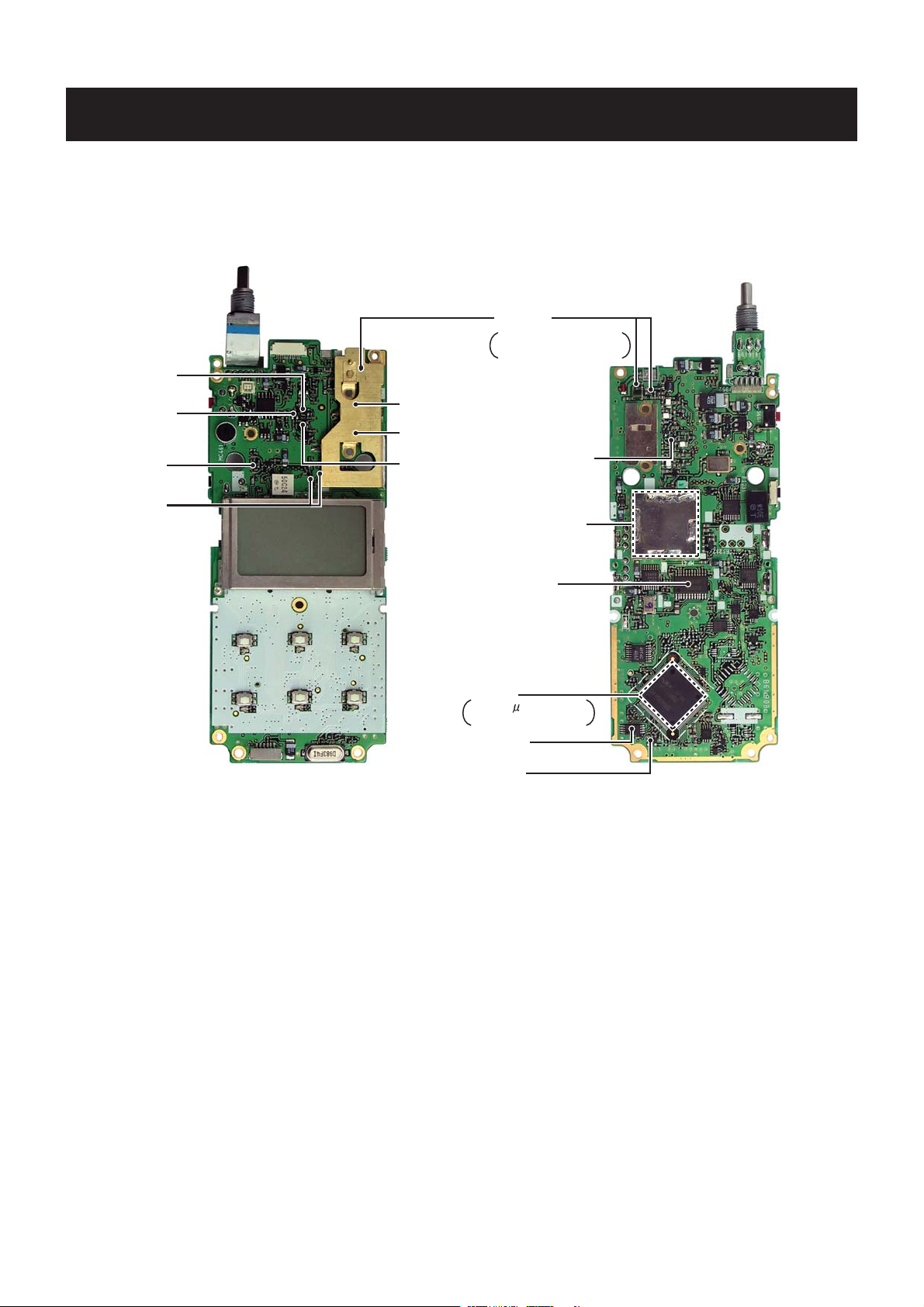
SECTION 2 INSIDE VIEWS
MAIN UNIT
•
TOP VIEW BOTTOM VIEW
S5V Regulator
(Q561: 2SA1588)
T5V Regulator
(Q323: 2SA1588)
IF amplifier
(Q211: 2SC4215)
TX/RX swith
(D91, D92: MA77)
Power amplifier
(*Q111: RD07MVS1)
Pre-drive
(*Q101: RD01MUS1)
R5 Regulator
(Q322: 2SA1588)
Antenna
Switches
*D131, D151: 1SV307
D152: MA2S077
RF amplifier
(Q165: 3SK294)
VCO circuits
*Located in under the plate.
D/A converter IC
(IC251: M62363FP-657C)
CPU
IC661: PD78F0338
GC-9EB
EEPROM
(IC591: BR24L32FV-W)
Reset IC
(IC581: S-80942CNMC)
2 - 1
Page 7
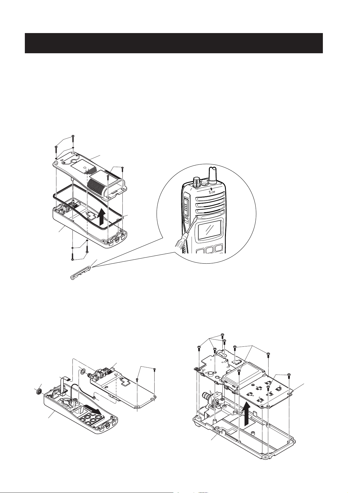
SECTION 3 DISASSEMBLY INSTRUCTIONS
REMOVING THE REAR PANEL
•
1 Remove the speaker panel A.
2 Unscrew 2 screws B, and remove 2 washers C.
3 Unscrew 2 screws D.
4 Unscrew 2 screws E, and remove 2 washers F.
5 Remove the rear panel and the main seal from the front
panel.
Note: When replacing the screws, 10–12 kg of torque MUST
be applied to ensure water resistance.
B
C
Rear panel
D
Main seal
Front panel
F
A
E
7!2.).'.%6%2ATTEMPTTOREMOVETHESPEAKERPANEL
R
USINGYOURFINGERNAILSTHISMAYRESULTINJURLY
5SEAFLATHEADSCREWDRIVERORASIMILAR
FLATINSTRUMENT
REMOVING THE CHASSIS UNIT
•
1 Unscrew 1 nut G.
2 Unscrew 2 screws H.
3 Take off the chassis unit in the direction of the arrow.
4 Unplug the connector I and the cable J from the
chassis unit.
5 Remove 1 washer K.
#)-
0
3
REMOVING THE MAIN UNIT
•
1 Unscrew 9 screws L.
2 Unsolder 2 points M, and take off the main unit in the
direction of the arrow.
L
L
F
Front panel
G
K
Chassis unit
I
H
L
Main unit
M
Chassis unit
3 - 1
Page 8
SECTION 4 CIRCUIT DESCRIPTION
4-1 RECEIVER CIRCUITS
4-1-1 ANTENNA SWITCHING CIRCUIT
The antenna switching circuit toggles receive line and
transmit line. This circuit does not allow transmit signals to
enter the receiver circuits.
Received signals from the antenna are passed through the
low-pass filter (LPF: L131, L132, C131–C136) and applied
to the antenna switching circuit (D151, D152).
While receiving, no voltage is applied to D151 and D152.
Thus, the receive line and the ground are disconnected and
L151, L152, C151, C152 and C153 function as an LPF which
leads received signals to the RF circuits.
4-1-2 RF CIRCUITS
The RF circuits amplify signals within the range of frequency coverage and filters off out-of-band signals.
The signals from the antenna switching circuit are passed
through the two-stage tunable bandpass filter (BPF: D154,
D155, L154–L156, C156, C157, C159–C161, C163, C164,
C168), then applied to the RF amplifier (Q165).
The amplified signals are passed through another two-stage
BPF (D181, D182, L166, L181 C181, C182, C184–C186,
C188) to suppress unwanted signals. The filtered signals are
then applied to the 1st mixer circuit.
The 1st IF signal from the 1st mixer is passed through the
crystal filter (FI211) to suppress unwanted signals, and
amplified at the 1st IF amplifier (Q211).
The amplified 1st IF signal is applied to the FM IF IC
(IC231).
4-1-4 2nd IF AND DEMODULATOR CIRCUITS
The 1st IF signal is converted into the 2nd IF signal and
de-modulated by the FM IF IC. The FM IF IC contains
2nd mixer, limiter amplifier, quadrature detector, etc. in its
package.
The 1st IF signal from the 1st IF amplifier is applied to pin
16 of IC231, and mixed with the 30.6 MHz 2nd LO signal
coming from the doubler (Q221), to convert into the 450 kHz
2nd IF signal and output from pin 3. The 2nd IF signal is
filtered by the ceramic filters (FI231, FI232) to suppress the
heterodyne noise, then applied to IC231 (pin 5) again and
amplified at the limiter amplifier section and demodulated by
the quadrature detector.
The quadrature detector is a detection method which uses a
ceramic discriminator (X231). The demodulated AF signals
are output from pin 9.
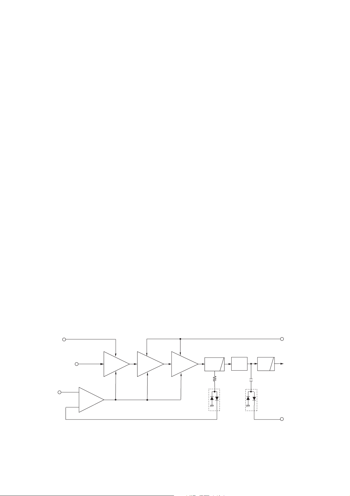
4-1-5 AF CIRCUITS
Demodulated signals are filtered and amplified at the AF
circuits.
4-1-3 1st MIXER AND 1st IF AMPLIFIER CIRCUITS
The 1st mixer circuit converts received signals into the
1st intermediate frequency (IF) signal by mixing with local
oscillator (LO) signal. The converted 1st IF signal is filtered
at the 1st IF filter, then amplified at the 1st IF amplifier.
The signals from the two-stage BPF are converted into the
31.05 MHz 1st IF signal at the 1st mixer (Q191) by being
mixed with the 1st LO signals generated at RX VCO (Q41,
D31–D34).
• 2nd IF AND DEMODULATER CIRCUITS
"SQCON" signal
from the D/A converter (IC251)
87
Noise
Active
filter
FM
detector
AF "DET" signal
to the AF circuits
AMP
Limiter
AMP
11109
X231
AF signals from IC231 (pin 9) are passed through the AF
mute switch (IC281 A; pins 1, 2), analog switch (IC282; pins
1, 7), LPF (IC261 C; pins 8–10) and R801 (VR BOARD) to
control the AF output level.
The level controlled AF signals are passed through the AF
mute switch (Q411) and the de-emphasis circuit (R411,
C413) to obtain the frequency characteristic of –6 dB/oct.
The de-emphasized signals are applied to the AF power
amplifier (IC421, pin 4). The AF power amplifier provides
more than 0.3 W of audio power.
450 kHz 2nd IF filters
FI232
D232
5
W/N
SW
Noise
detector
W/N
SW
D231
Noise
comparator
FI231
30.6 MHz 2nd LO signal
2
3
Mixer
×2
Q221
PLL
IC
(IC1)
2
1
IC231 TA31136FN
14
"NOISV" signal to the CPU (IC661, pin 32)
R5V
16
1st IF signal
from the IF amplifier (Q211)
X1
15.3 MHz
4 - 1
Page 9
4-1-6 SQUELCH CIRCUIT
Squelch circuit mutes AF output signal when no signals are
received.
4-2-2 MODULATOR CIRCUIT
The modulation circuit modulates the VCO oscillating signal
with the audio signals from the microphone.
A portion of the AF signals from the FM IF IC (IC231, pin 9) are
applied to the IC251 to control the level, and the active filter
(R239–R241, C237, C238). The filtered signals are applied to
the noise amplifier section in the FM IF IC (IC231, pin 8) to
amplify the noise components only.
The amplified noise components are detected at the noise
detector section, and output from pin 14 as the "NOISV"
signal to the CPU (IC661, pin 32). Then the CPU outputs
"AFMS" signal from pin 84 according to the "NOISV" signal
level to control the AF mute switch (Q411).
4-2 TRANSMITTER CIRCUITS
4-2-1 MIC AMPLIFIER, SPLATTER FILTER CIRCUITS
The MIC amplifier circuit amplifies audio signals from the
microphone within +6 dB/oct pre-emphasis characteristics
and amplifies to the level needed for modulation.
The AF signals from the microphone are passed through
the microphone switch (Q461) and the microphone mute
switches (IC682 A, pins 1, 2; IC682 B, pins 5, 6). The AF
signals are then passed through the pre-emphasis circuit
(R463, C463) to obtain frequency characteristics of +6 dB/oct.
The pre-emphasized AF signals are amplified at the
microphone amplifier (IC261 B), and adjusted its level at the
microphone gain control circuit (Q653, Q654, R474, R705,
R707, R708). The level adjusted signals are applied to the
limiter amplifier (IC491 A; pins 1, 2) to limit its level via the
AF mute switch (IC481 A; pins 1, 2).
The AF signals are then passed through the splatter filter
(IC491 B; pins 6, 7) to suppress unwanted 3 kHz and higher
audio signals, then applied to the modulation circuit via the
D/A converter (IC251; pins 3, 4).
AF signals from the D/A converter (IC251, pin 3) are applied
to the modulation circuit (D39) to modulate the oscillated
signal by changing the reactance of D39 at the TX VCO (Q51,
D35–38).
4-2-3 TRANSMIT AMPLIFIERS
Transmit amplifiers amplify the TX VCO output to transmit
power level.
The TX VCO output signal is buffer-amplified by the buffer
amplifiers (Q61, Q62) and passes through the TX/RX switch
(D91). The signals from the TX/RX switch are applied to the
another buffer amplifier (Q91), pre-drive (Q101) and power
amplifier (Q111) and amplified to the transmit level.
The power amplifier output is applied to the antenna
connector (J41: CHASSIS UNIT) via the antenna switching
circuit and the LPFs.
4-2-4 APC CIRCUIT
The APC (Automatic Power Control) circuit stabilizes
transmit output power and controls transmit output power
High, Middle and Low.
The RF output signal from the power amplifier (Q111)
is detected at the power detector (D121). The detector
converts the RF signals into DC voltage, and the detected
voltage is applied to the APC amplifier (IC141, pin 3).
The transmit output power setting voltage is applied to
another input terminal of the APC amplifier (IC141, pin 1) as
the reference voltage. The APC amplifier controls the bias of
the buffer, pre-drive and power amplifiers by comparing the
detected voltage and reference voltage. Thus the APC circuit
maintains a constant output power.
• APC CIRCUIT
T5V
RF signals
from TX/RX SW
T1CON
Another power detector (D132) detects the RF output level
and outputs "TDETV" signal to the CPU (IC661, pin 31). The
CPU outputs "TLED" signal to the LED driver (Q655) to light
TX LED (DS655).
VCC
Powe r
AMP
Q111
D121
LPF
ANT
SW
D132
LPF
To ANT
TDETV
Q91
Buffer
AMP
1
IC141
+
APC
AMP
3
–
4
Q101
Predrive
4 - 2
Page 10
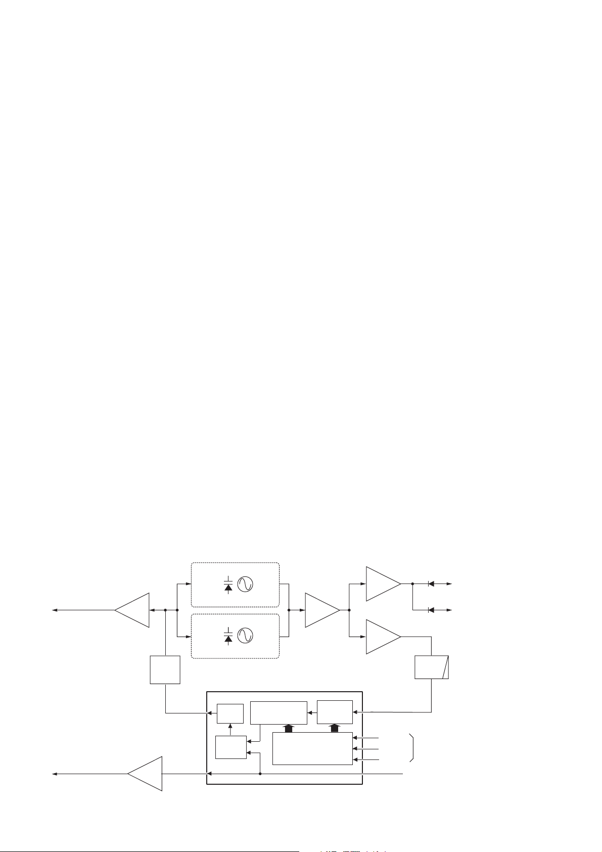
4-3 PLL CIRCUITS
4-3-1 GENERAL
PLL circuits control TX and RX VCO circuits. IC1 is a
PLL IC and contains prescaler, programmable counter,
programmable divider, phase detector, charge pump in its
package.
The VCOs directly generate the transmit frequency and the
1st LO frequency for receiving. The PLL sets the divided
ratio based on the serial data from the CPU (IC661), and
compares the phase of the VCO output with the reference
oscillator's frequency (15.3 MHz) oscillated by X1.
If the oscillated signal drifts, the phase of its frequency
changes from the phase of the reference frequency, causing
a lock voltage change to compensate for the drift in the
oscillated frequency.
4-3-2 TRANSMIT LOOP
A portion of the generated signal at the TX VCO (Q51, D35–
D39) is applied to the PLL IC (IC1, pin 8) via buffer-amplifier
(Q71). The applied signal is divided at the prescaler section
and programmable divider section and is then applied to the
phase detector section.
The phase detector compares the input signal with the
reference frequency, and then outputs the control signal
(pulse-type) from pin 5 via the charge pump section. The
pulse-type signal is converted into DC voltage at the loop
filter (R17–R19, C16, C17), and then applied to the TX VCO
(Q51, D35–D39) as the lock voltage.
The phase detector compares the input signal with a
reference frequency, and then outputs the control signal
(pulse-type) from pin 5. The pulse-type signal is converted
into DC voltage at the loop filter (R17–R19, C16, C17), and
then applied to the RX VCO (Q41, D31–D34) as the lock
voltage.
4-3-3 RECEIVE LOOP
The generated signal at the RX VCO (Q41, D31–D34) is
applied to the PLL IC (IC1, pin 8) via buffer-amplifier (Q71)
and is divided at the prescaler section and programmable
divider section and is then applied to the phase detector
section.
• PLL CIRCUITS
RX VCO
Buffer
"LOINV" signal
to the CPU (IC661, pin 34)
30.6 MHz 2nd LO
signal to the FM IF IC
(IC231, pin 2)
Q221
Q3
Loop
filter
×2
Q41, D31–D34
TX VCO
Q51, D35–D39
5
Charge
pump
Phase
detector
2
Programmable
divider
Buffer
Q61
IC1 MB15A02PFV
Prescaler
Shift register
Buffer
Q62
Buffer
Q71
8
9
10
11
1
D92
to 1st mixer circuit
D91
to transmitter circuit
LPF
SCLK
S DATA O
PLSTBO
PLL control signals
from D/A converter (IC251, pins 6–7)
15.3 MHz reference signal
from reference frequency osciilator (X1)
4 - 3
Page 11

4-4 POWER SUPPLY CIRCUITS
4-4-1 VOLTAGE LINES
LINE DESCRIPTION
The voltage from the connected DC power
VCC
CPU5V
M5V
T5V
S5V
R5V
supply passed through the [VOL] switch (R1:
VR BOARD).
5V for the CPU (IC661) converted from the
VCC line at the CPU5V regulator circuit (IC551).
Common 5V line converted from the VCC line
at the M5V regulator circuit (Q551–Q553).
5V for the transmit circuits controlled by the
T5V control circuit (Q323) using the T5VS
signal from the CPU (IC661, pin 90).
5V for the AF circuits controlled by the S5V
control circuit (Q561) using the S5VS signal
from the CPU (IC661, pin 87).
5V for the receive circuits controlled by the R5V
controll circuit (Q322) using the R5VS signal
from CPU (IC661, pin 89).
4-5 PORT ALLOCATIONS
4-5-1 CPU (IC661)
PIN
NUMBER
1 BEEP
3 EXSTB
4 DASTB
5 PLSTB
6 ERXDI
7 ETXDO
10 SDATA
11 SCK
12 ESCK
13 ESDA
14 TLED
15 RLED
17 CSIFT
25 RESET
27 WDECV
28 EXDET
29 VOXT
30 BATTV
31 TDETV
32 NOISV
33 RSSIV
34 LOINV
35 TEMPV
75, 76 CONT1, CONT2
PORT
NAME
DESCRIPTION
Output port for BEEP signal.
Output port for external expander
strobe signal.
Output port for external D/A strobe
signal.
Output port for PLL strobe.
Input port for cloning.
Output port for cloning.
Output port for serial data.
Output port for serial clock.
Input port for EEPROM clock.
I/O port for EEPROM data.
Output port for TX LED driver.
Output port for RX LED driver.
Output port for clock shift signal.
Input port for reset signal.
Input port for WX tone signal.
Input port for the [MIC/SP] detect
signal.
Input port for VOX signal.
Input port for battery voltage
detection signal.
Input port for TX power level.
Input port for noise level.
Input port for RSSI level.
Input port for PLL lock voltage level.
Input port for temperture level.
Output ports for LCD contrast
control signal.
PIN
NUMBER
PORT
NAME
77, 78 LEDS1, LEDS2
80 MICMS
81 ISPMS
84 AFMS
85 AFVS
102 PTTIN
103 EXPTT
104 BTYPE
105 PTTM
106–108 MIC1–MIC3
109 SQL
110 UP
111 DOWN
112 CH/WX
113 16/9
114 SCAN
115 H/L
117 VOXM
119 UNLK
4-5-2 EXPANDER (IC341)
PIN
NUMBER
6 DETMS
11 ATTS
12 TXMS
13 VCOS
14 SQLT
PORT
NAME
DESCRIPTION
Output port for dimmer control
signal.
Output port for microphone mute
signal.
"HIGH": Microphone mute
Output port for internal speaker
mute signal.
"HIGH": Speaker mute
Output port for AF mute signal.
Output port for AF amplifier power
supply control signal.
Input port for [PTT] switch.
Input port for external PTT switch.
Input port for battery type
detection.
Output port for microphone mute
signal.
Output ports for microphone
sensitivity detection signal.
Input port for [SQL] key.
Input port for [Y] key.
Input port for [Z] key.
Input port for [CALL] key.
Input port for [16] key.
Input port for [CH] key.
Input port for [Hi/Lo] key.
Ouput port for mute signal in VOX
mode.
Input port for PLL unlock signal.
DESCRIPTION
Output port for DET mute signal.
Output port for RF attenuator control
signal.
Output port for TX mute signal.
TX/RX VCO switching signal.
Output port for squelch control signal.
4 - 4
Page 12

SECTION 5 ADJUSTMENT PROCEDURES
5-1 PREPARATION
REQUIRED TEST EQUIPMENTS
When adjusting IC-GM1600/E, the optional CS-M90/GM1600 ADJ ADJUSTMENT SOFTWARE (Rev. 1.0 or later), OPC-478 (RS-232
type) or OPC-478U (USB type) CLONING CABLE, OPC-1028 and JIG cable (see page 5-2) are required.
EQUIPMENT GRADE AND RANGE EQUIPMENT GRADE AND RANGE
Measuring range : 0.1–3 W
RF power meter
(terminated type)
Frequency counter
FM deviation meter
Audio generator
STARTING SOFTWARE ADJUSTMENT
(1) Connect IC-GM1600/E and a PC with OPC-478/U,
OPC-1028 and JIG CABLE.
(2) Turn the transceiver ON.
(3) Boot up Windows
GM1600 ADJ’ in the ‘Programs’ folder of the [Start] menu,
then CS-M90/GM1600 ADJ’s window appears.
(4) Click ‘Adjust’ on the CS-M90/GM1600’s window, then
IC-GM1600/E’s up-to-date condition appears.
(5) Set or modify adjustment data as desired.
Frequency range : 100–300 MHz
Impedance : 50
SWR : Less than 1.2 : 1
Frequency range : 0.1–300 MHz
Frequency accuracy : ±1 ppm or better
Sensitivity : 100 mV or better
Frequency range : 30–300 MHz
Measuring range : 0 to ±10 kHz
Frequency range : 300–3000 Hz
Output level : 1–500 mV
®
, and click the program group 'CS-M90/
Ω
Standard signal
generator (SSG)
Oscilloscope
AC millivoltmeter Measuring range : 10 mV to 10 V
External speaker
Attenuator
Frequency range : 0.1–300 MHz
Output level : 0.1 µV to 32 mV
(–127 to –17 dBm)
Frequency range : DC–20 MHz
Measuring range : 0.01–20 V
Input impedance : 8
Capacity : More than 0.3 W
Power attenuation : 20 or 30 dB
Capacity : More than 5 W
Ω
CAUTION!: BACK UP the originally programmed memory
data in the transceiver before programming
the adjustment frequencies.
When program the adjustment frequencies
into the transceiver, the transceiver’s memory
data will be overwritten and lose original
memory data at the same time.
Microsoft and Windows are registered trademarks of
Microsoft Corporation in the U.S.A. and other countries.
5 - 1
Page 13

To [SP]
connector
• CONNECTION
AC millivoltmeter
Audio generator
to RS-232C port
to USB port
PC
SINAD meter
Speaker (8 Ω)
OPC-478 (RS-232C type)
OPC-478U (USB type)
To red line
To CLONE line
(BLACK)
(RED)
JIG cable
To MIC. line
(WHITE)
OPC-1028
to the antenna connector
Standard signal generator
0.1 µV to 32 mV
(–127 dBm to –17 dBm)
DO NOT transmit while
an SSG is connected to
the antenna connector.
Attenuator
20 dB / 30 dB
FM
deviation meter
RF power meter
0.1–3 W/50 Ω
Frequency
counter
• JIG CABLE
OPC-478/U
To [SP]
connector
(CLONE line)
IC-GM1600/E
To SINAD meter/speaker
To audio generator/AC millivoltmeter
(MIC. line)
(SP. line)
WHITE
RED
BLACK
OPC-1028
SHIELD
5 - 2
Page 14

• PC SCREEN EXAMPLE
q
w
e
r
t
I/O check button
i
y
u
o
NOTE: The above screen is an example.
Each transceiver has its own specific values for each setting.
q: Adjustment condition
w: Reference frequency
e: RF output power
r: FM deviation (Wide)
t: Receive sensitivity (Automaticaly)
y: Receive sensitivity (Manualy)
u: Squelch level
i: S-meter
o: VOX
5 - 3
Page 15

5-2 SOFTWARE ADJUSTMENT (FREQUENCY)
Select the adjustment item with [↑] / [↓] keys, then set the value with [←] / [→] keys on the connected PC.
MEASUREMENT
ADJUSTMENT ADJUSTMENT CONDITION
UNIT OPERATION
VALUE
PLL LOCK
VOLTAGE
REFERENCE
FREQUENCY
[Ref. Freq.]
1 • Operating CH. : 16
• Receiving
2 • Operating CH. : 16
• RF power : Low
• Transmitting
1 • Operating CH. : 16
• Connect the RF power meter or a 50
dummy load to the antenna connector.
• RF power : Low
• Transmitting
PC
screen
To p
Panel
Ω
Check the LVIN Data cell's
value in the I/O check
window.
Click the "I/O check button"
on the CS-M90/GM1600
ADJ's screen (see page
5-3) to open the I/O check
window as below.
Loosely couple the frequency
counter to the antenna
conector.
1.5–3.0 V [USA]
1.85–3.35 V [Others]
(Verify)
1.4–2.9 V
(Verify)
156.8000 MHz
±500 Hz
NOTE: The above screen is an example.
Each transceiver has its own specific values.
PLL LOCK VOLTAGE
5 - 4
Page 16

5-2 SOFTWARE ADJUSTMENT (TRANSMITTING)
Select the adjustment item with [↑] / [↓] keys, then set the value with [←] / [→] keys on the connected PC.
MEASUREMENT
ADJUSTMENT ADJUSTMENT CONDITION
UNIT OPERATION
VALUE
OUTPUT POWER
[RF Power (High)]
[RF Power (Low)] 2 • Operating CH. : 16
FM DEVIATION
[MOD (Wide)]
VOX
[VOX]
1 • Operating CH. : 16
• RF power : High
• Transmitting
• RF power : Low
• Transmitting
1 • Operating CH. : 16
• Set the FM deviation meter as;
HPF : OFF
LPF : 20 kHz
De-emphasis : OFF
Detector : (P±P)/2
• Connect the audio generator to
the [MIC/SP] jack through OPC-1028
and set as;
Frequency : 1 kHz
Level : 25 mV rms
• Transmitting
1 • Operating CH. : 16
• Set to VOX mode.
(Push [SQL] + [Hi/Lo]
• No audio applied to the [MIC/SP]
jack.
Top
Connect the RF power meter to
panel
panel
screen
.)
the antenna connector. 2.0 W
Top
Connect the FM deviation meter
to the antenna connector through
the attenuator.
Push the [ENTER] key on the keyboad
PC
of the connected PC.
0.75 W
±4.15–4.25 kHz
Automatic
adjustment
5 - 5
Page 17

5-2 SOFTWARE ADJUSTMENT (RECEIVING)
Select the adjustment item with [↑] / [↓] keys, then set the value with [←] / [→] keys on the connected PC.
ADJUSTMENT ADJUSTMENT CONDITION
UNIT
RECEIVE
SENSITIVITY
[BPF T1]
[BPF T2]
[BPF T3]
[BPF T4]
SQUELCH
LEVEL
[Noise]
S-METER
[RSSI]
*The output level of the standard signal generator (SSG) is indicated as the SSG's open circuit.
1
• Operating
• Connect the standard signal
generator to the antenna connector
and set as;
Frequency : 156.800 MHz
Level : +20 dBµ*
Modulation : 1 kHz
Deviation : ±3.0 kHz
• Receiving
CONVENIENT:
RECEIVE SENSITIVITY can be adjusted automatically.
1. Put the cursor on the [BPF ALL Sweep] on the CS-M90/GM1600 ADJ's screen and push the [ENTER] key.
2. The connected PC tunes BPF T1−T4 to peak level automaticaly.
or
1. Put the cursor on the one of BPF T1−T4 as desired.
2. Push the [ENTER] key to start tuning.
3. Repeat 1 and 2 to perform additional BPF tuning.
1
• Operating
• Connect the standard signal
generator to the antenna connector
and set as;
Frequency : 156.800 MHz
Level : –5 dBµ* [USA]
–6 dBµ* [Others]
Modulation : 1 kHz
Deviation
• Receiving
1
• Operating
• Connect the standard signal
generator to the antenna connector
and set as;
Frequency : 156.800 MHz
Level : –5 dBµ* [USA]
–4 dBµ* [Others]
Modulation : 1 kHz
Deviation : ±3.0 kHz
• Receiving
CH.
CH.
CH.
: 16
: 16
: ±3.0 kHz
: 16
To p
pannel
Top
panel
Top
panel
MEASUREMENT
OPERATION
Connect the distortion meter with an 8 Ω
load to the [MIC/SP] jack through the
JIG cable.
Push the [ENTER] key
of the connected PC.
Push the [ENTER] key
of the connected PC.
on the keyboad
on the keyboad
VALUE
Minimum
distortion level
Automatic
adjustment
Automatic
adjustment
5 - 6
Page 18

SECTION 6 PARTS LIST
• IC-GM1600/E
[MAIN UNIT]
REF ORDER
NO. NO.
IC1 1140005990 S.IC MB15A02PFV1-G-BND-ER B 55.7/12.1
IC141 1110002750 S.IC TA75S01F (TE85R) T 107.2/24.2
IC231 1110003201 S.IC TA31136FNG (EL) B 76.4/36.5
IC251 1190000350 S.IC M62363FP-650C B 53.5/24.2
IC261 1110005340 S.IC NJM12902V-TE1 B 56.1/41.6
IC281 1130007301 S.IC TC4W66FU F(TE12L) T 59/38.1
IC282 1130006220 S.IC TC4W53FU (TE12L) T 61.1/42.4
IC341 1130007570 S.IC BU4094BCFV-E2 B 33/8.6
IC382 1110003800 S.IC NJM2904V-TE1 B 33.1/34
IC383 1130007990 S.IC TC3W03FU (TE12L) B 9.5/38.5
IC421 1110001811 S.IC TA7368F G (ER) T 102.1/34.9
IC481 1130007301 S.IC TC4W66FU F (TE12L) B 46/37.6
IC491 1110003800 S.IC NJM2904V-TE1 B 41/32.8
IC551 1110005350 S.IC NJM2870F05-TE1 T 94.5/35.1
IC581 1110005770 S.IC S-80942CNMC-G9C-T2 B 6.8/12.4
IC591 1130011570 S.IC BR24L32FV-WE2 B 10.3/6.6
IC661 1140012420 S.IC µPD78F0338GC-9EB B 20/18.6
IC681 1130007301 S.IC TC4W66FU F(TE12L) B 8.8/28.7
IC682 1130007301 S.IC TC4W66FU F(TE12L) B 44.6/42.9
IC683 1110002750 S.IC TA75S01F (TE85R) B 37.1/42.8
Q3 1560000540 S.FET 2SK880-Y (TE85R) B 47.8/6
Q41 1530002920 S.TR 2SC4226-T1 R25 B 78.1/11.7
Q47 1590001190 S.TR XP6501-(TX) AB B 78.2/3.8
Q51 1530002920 S.TR 2SC4226-T1 R25 B 74.5/16.2
Q61 1530002380 S.TR 2SC4215-Y (TE85R) B 78.1/17.5
Q62 1530002380 S.TR 2SC4215-Y (TE85R) B 76.8/23.2
Q71 1530002380 S.TR 2SC4215-Y (TE85R) B 66.3/23.2
Q81 1590001400 S.TR XP1214 (TX) T 72.2/17.3
Q82 1590003290 S.TR UNR9213J-(TX) T 72.2/19.9
Q91 1530003420 S.TR 2SC5110-O (TE85R) T 82.3/8.9
Q101 1560001240 S.FET RD01MUS1 T 93.9/10.4
Q111 1560001230 S.FET RD07MVS1 T 100.1/10
Q141 1590003230 S.TR UNR9113J-(TX) T 110/23
Q165 1580000751 S.FET 3SK294 E (TE85L) B 96.3/19
Q171 1560000840 S.FET 2SK1829 (TE85R) B 98.9/17.1
Q191 1580000760 S.FET 3SK299-T1 U73 B 86.5/19.6
Q211 1530002600 S.TR 2SC4215-O (TE85R) T 84.5/37.9
Q221 1530002690 S.TR 2SC4116-GR (TE85R) B 65.1/30.3
Q231 1590003230 S.TR UNR9113J-(TX) T 69.7/38.2
Q232 1530003310 S.TR 2SC5107-O (TE85R) T 85.4/34
Q291 1590001650 S.TR XP4601 (TX) T 59.1/32.5
Q321 1510000670 S.TR 2SA1588-GR (TE85R) T 93.3/23.3
Q322 1510000670 S.TR 2SA1588-GR (TE85R) T 96.9/24.1
Q323 1510000670 S.TR 2SA1588-GR (TE85R) T 99.7/26.5
Q324 1590001770 S.TR XP1213 (TX) B 81.1/29.8
Q381 1590003290 S.TR UNR9213J-(TX) B 5.7/37.2
Q411 1530003091 S.TR 2SC4213-B F (TE85R) T 96.3/31.1
Q431 1520000450 S.TR 2SB1132 T100 Q T 111.4/30.5
Q432 1590001190 S.TR XP6501-(TX) AB T 107.6/29.6
Q441 1530002850 S.TR 2SC4116-BL (TE85R) T 101.5/39.2
Q442 1560001330 S.FET RSR025N03 T 103.3/42.4
Q443 1560001330 S.FET RSR025N03 T 97.9/41.4
Q444 1590003290 S.TR UNR9213J-(TX) T 98.3/38.4
Q461 1590003380 S.TR UNR9111J-(TX) B 90.3/42.5
Q462 1590003380 S.TR UNR9111J-(TX) B 90/45.6
Q501 1590003290 S.TR UNR9213J-(TX) B 34.6/26.1
Q531 1590001770 S.TR XP1213 (TX) B 37.5/16.8
Q532 1530002850 S.TR 2SC4116-BL (TE85R) B 36.9/23
Q551 1520000450 S.TR 2SB1132 T100 Q B 101.1/39.9
Q552 1590001190 S.TR XP6501-(TX) AB B 102.2/35.5
Q553 1590003290 S.TR UNR9213J-(TX) B 98.6/35
Q561 1510000670 S.TR 2SA1588-GR (TE85R) T 100.5/23.8
Q651 1590001770 S.TR XP1213 (TX) B 27.3/27.8
Q652 1590000660 S.TR DTC144TU T106 B 6.4/33.7
Q653 1590001770 S.TR XP1213 (TX) B 52/35.6
Q654 1590003290 S.TR UNR9213J-(TX) B 53.5/33.1
Q655 1590001540 S.TR UMD6N TR T 112.4/20.6
Q656 1590003550 S.TR XP4313 (TX) B 3.6/31.2
D1 1790001250 S.DIO MA2S111-(TX) B 51.2/14.6
D31 1750000711 S.VCP HVC350B-E B 70.7/9.2
D32 1750000711 S.VCP HVC350B-E B 72/9.2
D33 1750000711 S.VCP HVC350B-E B 68.1/9.2
D34 1750000711 S.VCP HVC350B-E B 69.4/9.2
D35 1750000711 S.VCP HVC350B-E B 65.7/16
D36 1750000711 S.VCP HVC350B-E B 65.7/14.7
D37 1750000711 S.VCP HVC350B-E B 63.8/17.5
D38 1750000711 S.VCP HVC350B-E B 63.8/18.8
D39 1720000400 S.VCP 1SV245 (TPH3) T 66.4/20.1
D40 1790001620 S.DIO 1SV308 (TPL3) Except [USA] B 65.4/10
D41 1790000680 S.DIO SB20-03P-TD B 118.7/29.3
D91 1790000620 S.DIO MA77 (TX) T 82.5/18.4
DESCRIPTION
M.=Mounted side (T: Mounted on the Top side, B: Mounted on the Bottom side)
M.
H/V
LOCATION
[MAIN UNIT]
REF ORDER
NO. NO.
D92 1790000620 S.DIO MA77 (TX) T 81.3/22
D121 1790001670 S.DIO RB706F-40T106 T 108.3/15.9
D131 1750000580 S.DIO 1SV307 (TPH3) T 111.9/9.8
D132 1790001210 S.DIO 1SS375-TL T 114.3/14
D141 1790001240 S.DIO MA2S728-(TX) T 102.6/25.1
D151 1750000580 S.DIO 1SV307 (TPH3) B 113.2/8.5
D152 1790001260 S.DIO MA2S077-(TX) B 111.3/12.7
D153 1790001620 S.DIO 1SV308 (TPL3) B 112.9/15.1
D154 1750000711 S.VCP HVC350BTRF-E B 109.1/20.4
D155 1750000711 S.VCP HVC350BTRF-E B 104.1/21.6
D171 1790001250 S.DIO MA2S111-(TX) B 102/16.9
D181 1750000711 S.VCP HVC350BTRF-E B 93.5/21.5
D182 1750000711 S.VCP HVC350BTRF-E B 90.5/21.5
D231 1750000520 S.DIO DAN222TL T 76.1/41.2
D232 1750000520 S.DIO DAN222TL T 74.1/37.6
D601 1790001260 S.DIO MA2S077-(TX) T 7.3/12.6
D602 1750000370 S.DIO DA221 TL B 10/32.6
D603 1790001250 S.DIO MA2S111-(TX) B 34.6/42.1
FI211 2030000230 S.MLH FL-355 (31.05 MHz)
[GEN], [EUR], [UK] B 89.1/32.7
4580000160 S.FIL FL-377 MFT31P (31.05 MHZ) [USA] B 89.1/32.7
FI231 2020001270 CER CFWLB450KE2A-B0
FI232 2020001410 CER CFWLB450KGFA-B0
X1 6050011940 S.XTL CR-783 (15.3 MHz) B 47.6/11.9
X231 6070000190 S.DCR CDBCB450KCAY24-R0 T 79.2/30.1
X381 6050011560 S.XTL CR-746 (4.000 MHz) B 13.9/38.5
X601 6050011550 S.XTL CR-747 (9.8304 MHz) T 2.9/17.6
L31 6200005540 S.COL ELJNC R47K-F T 66.7/9.9
L32 6200007710 S.COL LQW2BHN27NJ01L
[GEN], [EUR], [UK] B 67.4/12.2
6200008090 S.COL LQW2BHN68NJ01L [USA] B 67.4/12.2
L33 6200005540 S.COL ELJNC R47K-F T 63.6/13.8
L34 6200007760 S.COL LQW2BHN82NJ01L B 63.5/15.2
L35 6200007730 S.COL LQW2BHN39NJ01L Except [USA] B 63.9/12.3
L41 6200007760 S.COL LQW2BHN82NJ01L B 71.5/12.2
L51 6200007770 S.COL LQW2BHNR10J01L B 68.6/17.2
L61 6200006980 S.COL ELJRE R10G-F B 76.6/19.9
L62 6200006980 S.COL ELJRE R10G-F B 74.2/22.3
L71 6200006980 S.COL ELJRE R10G-F B 68.4/21.3
L72 6200005720 S.COL ELJRE 33NG-F B 63.8/21.6
L81 6200007170 S.COL MLF1608A 3R3K-T T 74.9/12.3
L82 6200007170 S.COL MLF1608A 3R3K-T T 74.8/15.3
L92 6200006980 S.COL ELJRE R10G-F T 84.7/11.2
L102 6200007690 S.COL LQW2BHN18NJ01L T 93.9/15.2
L112 6200009240 S.COL 0.20-1.0-7TL 31N T 104.1/13.9
L121 6200010640 S.COL 0.26-1.0-3TL 8.5N T 102.9/5.2
L122 6200009450 S.COL 0.20-1.0-6TL 25N T 105.6/4.3
L123 6200008280 S.COL 0.30-1.7-7TL 50N T 110.1/5.9
L124 6200003711 S.COL NLV25T 2R7J 2.7U T 111.1/13
L131 6200009800 S.COL 0.26-1.1-7TR 30N B 112.1/4.6
L132 6200008580 S.COL 0.30-1.4-6TL 32N T 115.4/9.8
L151 6200008280 S.COL 0.30-1.7-7TL 50N B 110/8.7
L152 6200005740 S.COL ELJRE 47NG-F B 109.3/12
L153 6200003960 S.COL MLF1608A 1R0K-T B 112.9/16.5
L154 6200007750 S.COL LQW2BHN56NJ01L B 107.9/18
L155 6200007750 S.COL LQW2BHN56NJ01L B 103.7/17.3
L156 6200001770 S.COL ELJNC 47NK-F [GEN], [EUR], [UK] B 112.6/18.4
6200002150 S.COL ELJNC 56NK-F [USA] B 112.6/18.4
L165 6200003960 S.COL MLF1608A 1R0K-T B 97.3/24.7
L166 6200007750 S.COL LQW2BHN56NJ01L B 95.3/22.1
L181 6200007750 S.COL LQW2BHN56NJ01L B 89.6/17.9
L191 6200010960 S.COL C2520C-R47G-A (0.47U) B 83.1/21.7
L203 6200009180 S.COL ELJRE R10J-F3 B 84.7/16
L221 6200003960 S.COL MLF1608A 1R0K-T B 64.2/28.1
L222 6200004480 S.COL MLF1608D R82K-T B 69.6/28.9
R1 7030005100 S.RES ERJ2GEJ 154 X (150 kΩ) B 54/16.4
R2 7030007250 S.RES ERJ2GEJ 220 X (22 Ω) B 54.6/17.8
R4 7510001660 S.TMR NTCG16 4LH 473KT B 41.8/9.1
R5 7030003940 S.RES ERJ3GEYF 104 V (100 kΩ) B 43.8/8
R6 7030005110 S.RES ERJ2GEJ 224 X (220 kΩ) B 44.4/16.6
R9 7030005230 S.RES ERJ2GEJ 334 X (330 kΩ) B 43.9/15.1
R15 7030005050 S.RES ERJ2GEJ 103 X (10 kΩ) B 50/8.7
R16 7030005580 S.RES ERJ2GEJ 560 X (56 Ω) B 53.6/15.4
R17 7030004980 S.RES ERJ2GEJ 101 X (100 Ω) B 53.5/8.8
R18 7030005120 S.RES ERJ2GEJ 102 X (1 kΩ) B 53.5/7.8
R19 7030005000 S.RES ERJ2GEJ 471 X (470 Ω) B 54.9/8.3
R20 7030005120 S.RES ERJ2GEJ 102 X (1 kΩ) B 45.3/6.8
DESCRIPTION
S.=Surface mount
M.
LOCATION
H/V
6 - 1
Page 19

[MAIN UNIT]
REF ORDER
NO. NO.
R21 7030005050 S.RES ERJ2GEJ 103 X (10 kΩ) B 49.7/7.2
R22 7030005210 S.RES ERJ2GEJ 822 X (8.2 kΩ) B 45.8/4.5
R31 7030005530 S.RES ERJ2GEJ 100 X (10 Ω) T 64.1/9.9
R32 7030005120 S.RES ERJ2GEJ 102 X (1 kΩ) B 73.2/8.8
R33 7030005120 S.RES ERJ2GEJ 102 X (1 kΩ) B 68.8/15.1
R34 7030005530 S.RES ERJ2GEJ 100 X (10 Ω) T 63.6/11.2
R35 7030008300 S.RES ERJ2GEJ 184 X (180 kΩ) T 69.1/20.4
R36 7030005240 S.RES ERJ2GEJ 473 X (47 kΩ) T 68.8/21.9
R37 7030005090 S.RES ERJ2GEJ 104 X (100 kΩ) T 67.8/19.9
R38 7030005240 S.RES ERJ2GEJ 473 X (47 kΩ) T 63.9/23
R39 7030005090 S.RES ERJ2GEJ 104 X (100 kΩ) T 66.4/22.9
R40 7030005040 S.RES ERJ2GEJ 472 X (4.7 kΩ)
Except [USA] B 65.2/8.3
R41 7030006461 S.RES ERA3YED 152V B 77/9.2
R42 7030006571 S.RES ERA3YED 392V B 75.7/9
R43 7030009320 S.RES ERJ2GEJ 4R7 X (4.7 Ω) B 76.3/11.4
R47 7030007290 S.RES ERJ2GEJ 222 X (2.2 kΩ) B 80.2/3.2
R51 7030006601 S.RES ERA3YED 272V B 74.3/14.3
R52 7030005331 S.RES ERA3YED 562V B 71.3/15.2
R53 7030009320 S.RES ERJ2GEJ 4R7 X (4.7 Ω) B 72.5/15.6
R61 7030004980 S.RES ERJ2GEJ 101 X (100 Ω) B 75.3/19.7
R62 7030005070 S.RES ERJ2GEJ 683 X (68 kΩ) B 76.3/17.6
R63 7030009320 S.RES ERJ2GEJ 4R7 X (4.7 Ω) B 72/22.9
R64 7030005240 S.RES ERJ2GEJ 473 X (47 kΩ) B 75/23.8
R65 7030004980 S.RES ERJ2GEJ 101 X (100 Ω) B 75/21.1
R71 7030005070 S.RES ERJ2GEJ 683 X (68 kΩ) B 69.1/23.6
R72 7030004990 S.RES ERJ2GEJ 221 X (220 Ω) B 69.6/21.6
R81 7030007280 S.RES ERJ2GEJ 331 X (330 Ω) T 72.9/12.9
R82 7030009280 S.RES ERJ2GEJ 391 X (390 Ω) T 73.5/14.8
R83 7030005040 S.RES ERJ2GEJ 472 X (4.7 kΩ) T 70/18.4
R84 7030005040 S.RES ERJ2GEJ 472 X (4.7 kΩ) T 69.1/19.4
R91 7030005120 S.RES ERJ2GEJ 102 X (1 kΩ) T 80.5/20.2
R92 7030004980 S.RES ERJ2GEJ 101 X (100 Ω) T 85/16.2
R93 7030005050 S.RES ERJ2GEJ 103 X (10 kΩ) T 84.3/17.2
R94 7030005030 S.RES ERJ2GEJ 152 X (1.5 kΩ) T 81.2/10.7
R95 7030005000 S.RES ERJ2GEJ 471 X (470 Ω) T 83.1/10.7
R96 7030007300 S.RES ERJ2GEJ 332 X (3.3 kΩ) T 83.1/11.7
R97 7030005530 S.RES ERJ2GEJ 100 X (10 Ω) T 86.1/11.8
R98 7030004980 S.RES ERJ2GEJ 101 X (100
R101 7030005040 S.RES ERJ2GEJ 472 X (4.7 kΩ) T 91.1/5.1
R102 7030005060 S.RES ERJ2GEJ 333 X (33 kΩ) T 91.6/3.7
R103 7030005590 S.RES ERJ2GEJ 680 X (68 Ω) T 92/6.6
R111 7030003200 S.RES ERJ3GEYJ 100 V (10 Ω) T 96.9/5.5
R112 7030005530 S.RES ERJ2GEJ 100 X (10 Ω) T 96.9/4.3
R113 7030005040 S.RES ERJ2GEJ 472 X (4.7 kΩ) T 93/4.3
R114 7030005090 S.RES ERJ2GEJ 104 X (100 kΩ) T 93/3.2
R121 7030003580 S.RES ERJ3GEYJ 153 V (15 kΩ) T 110.2/16.1
R122 7030000280 S.RES MCR10EZHJ 150 Ω (151) T 112.8/17.3
R131 7030003670 S.RES ERJ3GEYJ 823 V (82 kΩ) B 116.7/8.9
R132 7030007340 S.RES ERJ2GEJ 153 X (15 kΩ) T 115.4/17.4
R133 7030005050 S.RES ERJ2GEJ 103 X (10 kΩ) T 114.4/17.4
R141 7030005100 S.RES ERJ2GEJ 154 X (150 kΩ) T 104.3/25.4
R142 7030007350 S.RES ERJ2GEJ 393 X (39 kΩ) T 104.8/24
R143 7030007290 S.RES ERJ2GEJ 222 X (2.2 kΩ) T 107.7/21.6
R144 7030009140 S.RES ERJ2GEJ 272 X (2.7 kΩ) T 109.1/21.2
R145 7030008010 S.RES ERJ2GEJ 123 X (12 kΩ) T 109.2/19.8
R146 7030005050 S.RES ERJ2GEJ 103 X (10 kΩ) T 107.8/20.3
R147 7030005100 S.RES ERJ2GEJ 154 X (150 kΩ) T 106.4/20.8
R148 7030004980 S.RES ERJ2GEJ 101 X (100 Ω) T 104.8/22.1
R149 7030005120 S.RES ERJ2GEJ 102 X (1 kΩ) T 104.2/20.6
R151 7030004980 S.RES ERJ2GEJ 101 X (100 Ω) B 111.6/13.9
R152 7030005090 S.RES ERJ2GEJ 104 X (100 kΩ)
[GEN], [EUR], [UK] B 114.8/17.5
7030005220 S.RES ERJ2GEJ 223 X (22 kΩ) [USA] B 114.8/17.5
R153 7030005110 S.RES ERJ2GEJ 224 X (220 kΩ) B 108.9/22.2
R154 7030005050 S.RES ERJ2GEJ 103 X (10 kΩ) B 107.4/23.2
R155 7030005110 S.RES ERJ2GEJ 224 X (220 kΩ) B 103.1/23.4
R156 7030005050 S.RES ERJ2GEJ 103 X (10 kΩ) B 101.7/23.8
R165 7030005090 S.RES ERJ2GEJ 104 X (100 kΩ) [USA] B 98.1/19.3
7030008290 S.RES ERJ2GEJ 183 X (18 kΩ)
[GEN], [EUR], [UK] B 98.1/19.3
R166 7030005100 S.RES ERJ2GEJ 154 X (150 kΩ)
[GEN], [EUR], [UK] B 97/16.6
7030005700 S.RES ERJ2GEJ 274 X (270 kΩ) [USA] B 97/16.6
R167 7030005000 S.RES ERJ2GEJ 471 X (470 Ω) B 98.6/21.4
R171 7030005050 S.RES ERJ2GEJ 103 X (10 kΩ) B 100.2/22.4
R172 7030005170 S.RES ERJ2GEJ 474 X (470 kΩ) B 101.9/18.6
R173 7030009290 S.RES ERJ2GEJ 562 X (5.6 kΩ) B 100.8/16.6
R174 7030007060 S.RES ERJ2GEJ 684X (680 kΩ)
Except [USA] B 96/16.6
R175 7030005050 S.RES ERJ2GEJ 103 X (10 kΩ) B 99.1/19.3
R181 7030009270 S.RES ERJ2GEJ 821 X (820 Ω) B 92.7/17.4
R182 7030005110 S.RES ERJ2GEJ 224 X (220 kΩ) B 93.1/23.7
R183 7030005050 S.RES ERJ2GEJ 103 X (10 kΩ) B 93.7/25.4
R184 7030005110 S.RES ERJ2GEJ 224 X (220 kΩ) B 90.5/23.7
R185 7030005050 S.RES ERJ2GEJ 103 X (10 kΩ) B 91.4/25.1
R191 7030005710 S.RES ERJ2GEJ 121 X (120 Ω) B 87.2/23.4
R192 7030004980 S.RES ERJ2GEJ 101 X (100 Ω) B 85.2/22
R193 7030007300 S.RES ERJ2GEJ 332 X (3.3 kΩ) B 82.8/17.8
R194 7030003520 S.RES ERJ3GEYJ 472 V (4.7 kΩ) B 87.2/16.8
R201 7030005120 S.RES ERJ2GEJ 102 X (1 kΩ) T 84.8/23.7
R202 7030005050 S.RES ERJ2GEJ 103 X (10 kΩ) T 83.5/22.8
R203 7030005000 S.RES ERJ2GEJ 471 X (470 Ω) T 87.2/22
DESCRIPTION
) T 80.9/7
Ω
M.=Mounted side (T: Mounted on the Top side, B: Mounted on the Bottom side)
M.
H/V
LOCATION
[MAIN UNIT]
REF ORDER
NO. NO.
R204 7030010430 S.RES ERJ2GEJ 120 X (12 Ω) T 85.9/20.8
R205 7030005000 S.RES ERJ2GEJ 471 X (470 Ω) T 86.4/19.5
R206 7030005040 S.RES ERJ2GEJ 472 X (4.7 kΩ) B 85.9/16.5
R211 7030005120 S.RES ERJ2GEJ 102 X (1 kΩ) B 85.9/25.2
R213 7030005030 S.RES ERJ2GEJ 152 X (1.5 kΩ)
[GEN], [EUR], [UK] T 88.3/38.5
7030005120 S.RES ERJ2GEJ 102 X (1 kΩ) [USA] T 88.3/38.5
R214 7030005000 S.RES ERJ2GEJ 471 X (470 Ω) T 85/35.9
R215 7030005310 S.RES ERJ2GEJ 124 X (120 kΩ) T 86.3/38.5
R216 7030005010 S.RES ERJ2GEJ 681 X (680 Ω) T 86.6/36.8
R221 7030007060 S.RES ERJ2GEJ 684X (680 kΩ) B 63.3/29.8
R222 7030007570 S.RES ERJ2GEJ 122 X (1.2 kΩ) B 62.3/29.8
R223 7030007270 S.RES ERJ2GEJ 151 X (150 Ω) B 81.3/38.2
R231 7030007300 S.RES ERJ2GEJ 332 X (3.3 kΩ) T 80.6/35
R232 7030004970 S.RES ERJ2GEJ 470 X (47 Ω) T 83.1/35.9
R233 7030007340 S.RES ERJ2GEJ 153 X (15 kΩ) T 76.1/43.4
R234 7030005220 S.RES ERJ2GEJ 223 X (22 kΩ) T 71.9/39.2
R235 7030005220 S.RES ERJ2GEJ 223 X (22 k
R236 7030009320 S.RES ERJ2GEJ 4R7 X (4.7 Ω) T 73.9/39.3
R237 7030008010 S.RES ERJ2GEJ 123 X (12 kΩ) T 71.9/38.2
R238 7030007340 S.RES ERJ2GEJ 153 X (15 kΩ) T 78.5/37.6
R239 7030005230 S.RES ERJ2GEJ 334 X (330 kΩ) B 80.7/34.3
R240 7030005600 S.RES ERJ2GEJ 273 X (27 kΩ) B 78.2/33.2
R241 7030007290 S.RES ERJ2GEJ 222 X (2.2 kΩ) B 82.9/36
R242 7030009280 S.RES ERJ2GE B 73.1/33.2
R243 7030009320 S.RES ERJ2GEJ 4R7 X (4.7 Ω) T 71.9/37.2
R244 7030007290 S.RES ERJ2GEJ 222 X (2.2 kΩ) T 82.6/34.6
R245 7030005240 S.RES ERJ2GEJ 473 X (47 kΩ) T 85.1/32.2
R246 7030005240 S.RES ERJ2GEJ 473 X (47 kΩ) T 86.8/31.1
R247 7030007570 S.RES ERJ2GEJ 122 X (1.2 kΩ)
[USA], [GEN] B 81.9/32.3
7030009140 S.RES ERJ2GEJ 272 X (2.7 kΩ)
[EUR], [UK] B 81.9/32.3
R251 7030005000 S.RES ERJ2GEJ 471 X (470 Ω) B 57.8/18.3
R261 7030005040 S.RES ERJ2GEJ 472 X (4.7 kΩ) B 62.8/36.5
R262 7030008010 S.RES ERJ2GEJ 123 X (12 kΩ) B 61.2/39.2
R263 7030005240 S.RES ERJ2GEJ 473 X (47 kΩ) B 60.8/37.8
R264 7030005210 S.RES ERJ2GEJ 822 X (8.2 kΩ) B 60.9/40.2
R264 7030010040 S.RES ERJ2GE-JPW B 60.9/40.2
R265 7030005050 S.RES ERJ2GEJ 103 X (10 kΩ) B 58.6/37.8
R266 7030009290 S.RES ERJ2GEJ 562 X (5.6 kΩ) B 59.8/38.3
R267 7030005050 S.RES ERJ2GEJ 103 X (10 kΩ) B 63.5/41.1
R269 7030005090 S.RES ERJ2GEJ 104 X (100 kΩ) B 57.6/37.8
R270 7030007340 S.RES ERJ2GEJ 153 X (15 kΩ) B 60.9/43.3
R271 7030005720 S.RES ERJ2GEJ 563 X (56 kΩ) B 63.4/43.1
R272 7030005100 S.RES ERJ2GEJ 154 X (150 kΩ) B 60.7/44.7
R273 7030005120 S.RES ERJ2GEJ 102 X (1 kΩ) B 59.7/45.3
R274 7030005120 S.RES ERJ2GEJ 102 X (1 kΩ) B 62.1/44.5
R275 7030008300 S.RES ERJ2GEJ 184 X (180 kΩ) T 56.6/41.3
R276 7030005050 S.RES ERJ2GEJ 103 X (10 kΩ) T 56.9/44.9
R277 7030006610 S.RES ERJ2GEJ 394 X (390 kΩ) T 55.5/43.5
R281 7030005090 S.RES ERJ2GEJ 104 X (100 kΩ) T 62.2/38.8
R282 7030005090 S.RES ERJ2GEJ 104 X (100 kΩ) T 57.8/35.7
R283 7030005090 S.RES ERJ2GEJ 104 X (100 kΩ) T 58.9/44.3
R284 7030005090 S.RES ERJ2GEJ 104 X (100 kΩ) T 59.7/35.7
R291 7030005070 S.RES ERJ2GEJ 683 X (68 kΩ) T 61.5/34.1
R292 7030005070 S.RES ERJ2GEJ 683 X (68 kΩ) T 62/32
R293 7030005070 S.RES ERJ2GEJ 683 X (68 kΩ) T 61/32
R294 7030005050 S.RES ERJ2GEJ 103 X (10 kΩ) T 63.4/29.6
R296 7030007340 S.RES ERJ2GEJ 153 X (15 kΩ) T 60/34.3
R297 7030005050 S.RES ERJ2GEJ 103 X (10 kΩ) T 56.1/31.7
R298 7030005040 S.RES ERJ2GEJ 472 X (4.7 kΩ) T 56.6/29.4
R305 7030005090 S.RES ERJ2GEJ 104 X (100 kΩ) T 60.5/30.5
R306 7030005070 S.RES ERJ2GEJ 683 X (68 kΩ) T 59.2/30.2
R307 7030007570 S.RES ERJ2GEJ 122 X (1.2 kΩ) T 57.1/32.2
R321 7030005050 S.RES ERJ2GEJ 103 X (10 kΩ) T 93.5/21.4
R322 7030005040 S.RES ERJ2GEJ 472 X (4.7 kΩ) T 91.5/23.2
R323 7030005050 S.RES ERJ2GEJ 103 X (10 kΩ) T 95.4/22.2
R324 7030005040 S.RES ERJ2GEJ 472 X (4.7 kΩ) T 95.1/23.7
R325 7030005050 S.RES ERJ2GEJ 103 X (10 kΩ) T 97.8/26.5
R326 7030005040 S.RES ERJ2GEJ 472 X (4.7 kΩ) T 96.8/26.5
R381 7030005050 S.RES ERJ2GEJ 103 X (10 kΩ) B 35.4/30.3
R382 7030005720 S.RES ERJ2GEJ 563 X (56 kΩ) B 33.2/29.6
R383 7030005090 S.RES ERJ2GEJ 104 X (100 kΩ) B 35.6/32
R384 7030008290 S.RES ERJ2GEJ 183 X (18 kΩ) B 30.6/34.1
R385 7030007300 S.RES ERJ2GEJ 332 X (3.3 kΩ) B 33/38.4
R386 7030005090 S.RES ERJ2GEJ 104 X (100 kΩ) B 36/35.7
R387 7030005160 S.RES ERJ2GEJ 105 X (1 MΩ) B 9.8/41.7
R388 7030005120 S.RES ERJ2GEJ 102 X (1 kΩ) B 7.2/40.2
R389 7030005050 S.RES ERJ2GEJ 103 X (10 kΩ) B 7.3/36.6
R390 7030010040 S.RES ERJ2GE-JPW [USA] only B 62.9/10.4
R391 7030010040 S.RES ERJ2GE-JPW T 83/14.8
R393 7030010040 S.RES ERJ2GE-JPW T 82.5/6.4
R394 7030010040 S.RES ERJ2GE-JPW T 89.2/4
R398 7030010040 S.RES ERJ2GE-JPW B 60.6/41.5
R399 7030010040 S.RES ERJ2GE-JPW T 58.9/42.5
R411 7030005050 S.RES ERJ2GEJ 103 X (10 kΩ) T 98.7/31.4
R412 7030005050 S.RES ERJ2GEJ 103 X (10 kΩ) T 94.3/32
R413 7030005060 S.RES ERJ2GEJ 333 X (33 kΩ) T 94.3/30.1
R414 7030007310 S.RES ERJ2GEJ 155 X (1.5 MΩ) T 99.2/29
R415 7030007310 S.RES ERJ2GEJ 155 X (1.5 MΩ) T 97.2/29
R421 7030005530 S.RES ERJ2GEJ 100 X (10 Ω) T 107/33.5
R422 7030005530 S.RES ERJ2GEJ 100 X (10 Ω) B 104.4/38.7
DESCRIPTION
) T 72.5/36
Ω
S.=Surface mount
M.
LOCATION
H/V
6 - 2
Page 20

[MAIN UNIT]
REF ORDER
NO. NO.
R431 7030005600 S.RES ERJ2GEJ 273 X (27 kΩ) T 106.1/27.6
R432 7030005160 S.RES ERJ2GEJ 105 X (1 MΩ) T 107.6/27.1
R433 7030007290 S.RES ERJ2GEJ 222 X (2.2 kΩ) T 109.4/33
R434 7030007290 S.RES ERJ2GEJ 222 X (2.2 kΩ) T 105.8/29.6
R435 7030007300 S.RES ERJ2GEJ 332 X (3.3 kΩ) T 108.1/32.1
R441 7030005170 S.RES ERJ2GEJ 474 X (470 kΩ) T 100.7/41
R442 7030005170 S.RES ERJ2GEJ 474 X (470 kΩ) T 96.7/38.3
R443 7030005090 S.RES ERJ2GEJ 104 X (100 kΩ) T 99.5/39.9
R461 7030005060 S.RES ERJ2GEJ 333 X (33 kΩ) B 94.3/48.5
R462 7030005040 S.RES ERJ2GEJ 472 X (4.7 kΩ) B 47.8/44.6
R463 7030009290 S.RES ERJ2GEJ 562 X (5.6 kΩ) B 50.3/42.8
R467 7030008280 S.RES ERJ2GEJ 271 X (270 Ω) B 97.3/40.8
R468 7030005090 S.RES ERJ2GEJ 104 X (100 kΩ) B 90.5/40.4
R471 7030007060 S.RES ERJ2GEJ 684X (680 kΩ) B 51.7/43.1
R472 7030008290 S.RES ERJ2GEJ 183 X (18 kΩ) B 56.2/38.3
R473 7030005040 S.RES ERJ2GEJ 472 X (4.7 kΩ) B 50.7/44.2
R474 7030009290 S.RES ERJ2GEJ 562 X (5.6 kΩ) B 50.2/40.3
R475 7030010310 S.RES ERJ3GEYF 223 V (22 kΩ) B 58/35.5
R476 7030004740 S.RES ERJ3GEYF 392 V (3.9 kΩ) B 57.2/33.5
R477 7030004730 S.RES ERJ3GEYF 222 V (2.2 kΩ) B 60.7/35.5
R481 7030005090 S.RES ERJ2GEJ 104 X (100 kΩ) B 47.3/35.4
R482 7030005090 S.RES ERJ2GEJ 104 X (100 kΩ) B 42.3/39
R490 7030005720 S.RES ERJ2GEJ 563 X (56 kΩ) B 39.3/37.5
R491 7030007340 S.RES ERJ2GEJ 153 X (15 kΩ) B 41.1/37.4
R492 7030005110 S.RES ERJ2GEJ 224 X (220 kΩ) B 37.4/25.8
R493 7030008310 S.RES ERJ2GEJ 564 X (560 kΩ) B 39.1/36.2
R494 7030005250 S.RES ERJ3GEYF 103 V (10 kΩ) B 44.4/33.6
R495 7030005040 S.RES ERJ2GEJ 472 X (4.7 kΩ) B 38.5/31.3
R496 7030005110 S.RES ERJ2GEJ 224 X (220 kΩ) B 38/29.3
R497 7030008300 S.RES ERJ2GEJ 184 X (180 kΩ) B 39.4/24.7
R498 7030005090 S.RES ERJ2GEJ 104 X (100 kΩ) B 39.4/25.7
R501 7030005090 S.RES ERJ2GEJ 104 X (100 kΩ) B 43.5/31
R502 7030005060 S.RES ERJ2GEJ 333 X (33 kΩ) B 40.7/27.3
R503 7030005310 S.RES ERJ2GEJ 124 X (120 k
R504 7030005050 S.RES ERJ2GEJ 103 X (10 kΩ) B 44.6/29.7
R511 7030005600 S.RES ERJ2GEJ 273 X (27 kΩ) B 33/23.6
R512 7030005100 S.RES ERJ2GEJ 154 X (150 kΩ) B 36.6/28
R513 7030008290 S.RES ERJ2GEJ 183 X (18 kΩ) B 32.6/25.6
R521 7030005010 S.RES ERJ2GEJ 681 X (680 Ω) B 45.1/31.1
R531 7030005220 S.RES ERJ2GEJ 223 X (22 kΩ) B 34.6/18.9
R532 7030005220 S.RES ERJ2GEJ 223 X (22 kΩ) B 33.4/15.5
R533 7030005720 S.RES ERJ2GEJ 563 X (56 kΩ) B 34.1/16.5
R534 7030008300 S.RES ERJ2GEJ 184 X (180 kΩ) B 34.1/17.5
R535 7030005050 S.RES ERJ2GEJ 103 X (10 kΩ) B 35.5/17.3
R536 7030005240 S.RES ERJ2GEJ 473 X (47 kΩ) B 36.3/18.9
R537 7030005240 S.RES ERJ2GEJ 473 X (47 kΩ) B 36.3/20.8
R538 7030005120 S.RES ERJ2GEJ 102 X (1 kΩ) B 35/23.4
R539 7030005240 S.RES ERJ2GEJ 473 X (47 kΩ) B 39.3/21.3
R540 7030007340 S.RES ERJ2GEJ 153 X (15 kΩ) B 39.3/22.3
R551 7030005050 S.RES ERJ2GEJ 103 X (10 kΩ) B 99.9/36.5
R552 7030007290 S.RES ERJ2GEJ 222 X (2.2 kΩ) B 100.4/35
R553 7030005220 S.RES ERJ2GEJ 223 X (22 kΩ) B 100.5/33.5
R561 7030005050 S.RES ERJ2GEJ 103 X (10 kΩ) T 100.3/21.8
R562 7030005040 S.RES ERJ2GEJ 472 X (4.7 kΩ) T 98.7/23.4
R571 7030005930 S.RES ERJ3GEYF 334 V (330 kΩ) B 105.2/30
R572 7030008090 S.RES ERJ3EKF 1503 V (150 kΩ) B 103.1/27.3
R581 7030005050 S.RES ERJ2GEJ 103 X (10 kΩ) B 9.2/12.3
R583 7030005090 S.RES ERJ2GEJ 104 X (100 kΩ) T 6.4/34.4
R584 7030005090 S.RES ERJ2GEJ 104 X (100 kΩ) T 6.9/33
R591 7030005050 S.RES ERJ2GEJ 103 X (10 kΩ) B 10.7/12.1
R592 7030005050 S.RES ERJ2GEJ 103 X (10 kΩ) B 8/9.6
R601 7030005530 S.RES ERJ2GEJ 100 X (10 Ω) T 6.6/17.4
R602 7030005160 S.RES ERJ2GEJ 105 X (1 MΩ) T 6.1/18.9
R603 7030008010 S.RES ERJ2GEJ 123 X (12 kΩ) T 7.8/15
R604 7030008010 S.RES ERJ2GEJ 123 X (12 kΩ) T 6.5/14.4
R605 7030008010 S.RES ERJ2GEJ 123 X (12 kΩ) T 7.3/10.3
R606 7030005120 S.RES ERJ2GEJ 102 X (1 kΩ) T 6.8/8.8
R611 7030005050 S.RES ERJ2GEJ 103 X (10 kΩ) T 54.8/42.5
R612 7030005040 S.RES ERJ2GEJ 472 X (4.7 kΩ) T 54.3/44.8
R631 7030005050 S.RES ERJ2GEJ 103 X (10 kΩ) B 25.5/7.6
R632 7030005090 S.RES ERJ2GEJ 104 X (100 kΩ) B 23.9/5.2
R633 7030005050 S.RES ERJ2GEJ 103 X (10 kΩ) B 15.9/6.7
R634 7030005050 S.RES ERJ2GEJ 103 X (10 kΩ) B 23.9/7.1
R635 7030005050 S.RES ERJ2GEJ 103 X (10 kΩ) B 17.1/5.8
R636 7030005050 S.RES ERJ2GEJ 103 X (10 kΩ) B 14.7/5.3
R637 7030005050 S.RES ERJ2GEJ 103 X (10 kΩ) B 14.3/6.6
R638 7030005050 S.RES ERJ2GEJ 103 X (10 kΩ) B 13.7/9.6
R639 7030005050 S.RES ERJ2GEJ 103 X (10 kΩ) B 12.7/9.8
R651 7030007280 S.RES ERJ2GEJ 331 X (330 Ω)
[USA], [GEN] T 63.1/4.3
7030005010 S.RES ERJ2GEJ 681 X (680 Ω) [Others] T 63.1/4.3
R652 7030004990 S.RES ERJ2GEJ 221 X (220 Ω) T 62.1/3.8
R653 7030005120 S.RES ERJ2GEJ 102 X (1 kΩ) T 15.8/38.2
R654 7030005010 S.RES ERJ2GEJ 681 X (680 Ω) T 14.8/38.2
R656 7030005120 S.RES ERJ2GEJ 102 X (1 kΩ) T 16.3/11.8
R657 7030005010 S.RES ERJ2GEJ 681 X (680 Ω) T 15.3/11.8
R658 7030005120 S.RES ERJ2GEJ 102 X (1 kΩ) T 16.2/22.7
R659 7030005010 S.RES ERJ2GEJ 681 X (680 Ω) T 15.2/22.7
R662 7030007280 S.RES ERJ2GEJ 331 X (330 Ω)
[USA], [GEN] T 68.9/4.3
7030005010 S.RES ERJ2GEJ 331 X (680 Ω) [Others] T 68.9/4.3
R663 7030004990 S.RES ERJ2GEJ 221 X (220 Ω) T 70.3/3.3
R681 7030009150 S.RES ERJ2GEJ 824 X (820 kΩ) B 12.7/27.2
DESCRIPTION
) B 38/27.2
Ω
M.=Mounted side (T: Mounted on the Top side, B: Mounted on the Bottom side)
M.
H/V
LOCATION
[MAIN UNIT]
REF ORDER
NO. NO.
R682 7030005700 S.RES ERJ2GEJ 274 X (270 kΩ) B 6.6/26.5
R683 7030006610 S.RES ERJ2GEJ 394 X (390 kΩ) B 12/29.3
R684 7030003830 S.RES ERJ3GEYJ 185 V (1.8 MΩ) B 13.2/29.7
R685 7030007340 S.RES ERJ2GEJ 153 X (15 kΩ) B 8.4/31.4
R686 7030005120 S.RES ERJ2GEJ 102 X (1 kΩ) B 8.1/33.2
R687 7030005120 S.RES ERJ2GEJ 102 X (1 kΩ) B 5.4/31.3
R688 7030005080 S.RES ERJ2GEJ 823 X (82 kΩ) B 4.3/34.2
R689 7030005240 S.RES ERJ2GEJ 473 X (47 kΩ) B 3.6/33.2
R690 7030010040 S.RES ERJ2GE-JPW B 47.7/31.3
R691 7030010040 S.RES ERJ2GE-JPW B 50.7/30.5
R692 7030010040 S.RES ERJ2GE-JPW T 5.4/38.7
R693 7030005120 S.RES ERJ2GEJ 102 X (1 kΩ) T 119.6/20.5
R694 7030005170 S.RES ERJ2GEJ 474 X (470 k
R695 7030005090 S.RES ERJ2GEJ 104 X (100 kΩ) B 88.9/47.7
R696 7030005090 S.RES ERJ2GEJ 104 X (100 kΩ) B 41.2/40.8
R697 7030005090 S.RES ERJ2GEJ 104 X (100 kΩ) B 48.2/40.8
R698 7030007340 S.RES ERJ2GEJ 153 X (15 kΩ) B 40.3/45.6
R699 7030005230 S.RES ERJ2GEJ 334 X (330 kΩ) B 38.3/45.6
R700 7030007570 S.RES ERJ2GEJ 122 X (1.2 kΩ) B 38.8/40.6
R701 7030006610 S.RES ERJ2GEJ 394 X (390 kΩ) B 36.9/40.6
R702 7030005220 S.RES ERJ2GEJ 223 X (22 kΩ) B 34.8/44.5
R703 7030003830 S.RES ERJ3GEYJ 185 V (1.8 MΩ) B 33.3/43.3
R704 7030005090 S.RES ERJ2GEJ 104 X (100 kΩ) B 11/31.1
R705 7030008290 S.RES ERJ2GEJ 183 X (18 kΩ) B 49.9/37.5
R706 7030008090 S.RES ERJ3EKF 1503 V (150 kΩ) B 44.4/35
R707 7030005210 S.RES ERJ2GEJ 822 X (8.2 kΩ) B 49.9/38.5
R708 7030008410 S.RES ERJ2GEJ 392 X (3.9 kΩ) B 49.8/36
R709 7030005040 S.RES ERJ2GEJ 472 X (4.7 kΩ) B 50.3/41.8
R710 7030005210 S.RES ERJ2GEJ 822 X (8.2 kΩ) B 51.7/40.1
R711 7030005090 S.RES ERJ2GEJ 104 X (100 kΩ) B 56.2/37.1
R712 7030005040 S.RES ERJ2GEJ 472 X (4.7 kΩ) B 52.6/37.9
R715 7030010040 S.RES ERJ2GE-JPW B 24.9/5.7
R717 7030010040 S.RES ERJ2GE-JPW B 28.9/10.1
R718 7030005120 S.RES ERJ2GEJ 102 X (1 kΩ) B 92.7/42.9
R720 7030010040 S.RES ERJ2GE-JPW B 45/45.5
C1 4030016930 S.CER ECJ0EB1A104K B 51/17.8
C2 4030016930 S.CER ECJ0EB1A104K B 52.6/17.8
C3 4030017460 S.CER ECJ0EB1E102K B 53.6/17.8
C4 4030017420 S.CER ECJ0EC1H470J B 55.8/16.4
C5 4030016930 S.CER ECJ0EB1A104K B 42.6/7.5
C6 4030018560 S.CER C2012 JB 1A 475K-T B 46.5/20
C10 4030016930 S.CER ECJ0EB1A104K B 46.3/8.8
C11 4030017460 S.CER ECJ0EB1E102K B 45.3/8.8
C12 4030007010 S.CER C1608 CH 1H 100D-T B 48.2/9.1
C13 4030017430 S.CER ECJ0EC1H101J B 51.2/10.6
C14 4030017460 S.CER ECJ0EB1E102K B 55.5/15.4
C16 4550006300 S.TAN ECST1AY475R B 51.6/6.7
C17 4550006160 S.TAN ECST1CY155R B 58/8.2
C19 4030017460 S.CER ECJ0EB1E102K B 45.3/5.8
C20 4030017460 S.CER ECJ0EB1E102K B 50/5.7
C21 4030017460 S.CER ECJ0EB1E102K B 44.8/4.5
C31 4030007040 S.CER C1608 CH 1H 180J-T B 69.8/12
C32 4030007000 S.CER C1608 CH 1H 090D-T B 67.6/14.9
C33 4030007070 S.CER C1608 CH 1H 330J-T B 65.9/18
C34 4030017460 S.CER ECJ0EB1E102K T 67.8/21.9
C35 4030017730 S.CER ECJ0EB1E471K T 65.4/22.9
C36 4030018860 S.CER ECJ0EB0J105K T 61.9/23
C37 4030009540 S.CER C1608 CH 1H 1R5B-T T 67.2/17.7
C38 4030018860 S.CER ECJ0EB0J105K Except [USA] B 63.2/8.3
C39 4030009920 S.CER C1608 CH 1H 050B-T Except [USA] B 66.7/9.9
C40 4030009350 S.CER C1608 CH 1H 3R5B-T Except [USA] B 64.1/10
C41 4030009550 S.CER C1608 CH 1H 2R5B-T B 74.4/9
C42 4030007090 S.CER C1608 CH 1H 470J-T B 74.4/11
C43 4030007020 S.CER C1608 CH 1H 120J-T B 74.4/12.3
C44 4030017730 S.CER ECJ0EB1E471K B 78.5/9.3
C45 4030016790 S.CER ECJ0EB1C103K B 78.5/8.3
C46 4030009560 S.CER C1608 CH 1H R75B-T B 78.7/14.6
C47 4550006700 S.TAN ECST1AY106R B 83.3/3
C48 4550006700 S.TAN ECST1AY106R B 74.1/3.6
C51 4030009560 S.CER C1608 CH 1H R75B-T B 68.8/18.9
C52 4030009920 S.CER C1608 CH 1H 050B-T B 70/14.9
C52 4030011770 S.CER C1608 CH 1H 060B-T B 70/14.9
C53 4030007050 S.CER C1608 CH 1H 220J-T B 71.7/17.2
C54 4030007040 S.CER C1608 CH 1H 180J-T B 71.7/18.5
C55 4030017730 S.CER ECJ0EB1E471K B 76.9/14.5
C56 4030016790 S.CER ECJ0EB1C103K B 76.9/15.5
C57 4030009500 S.CER C1608 CH 1H 0R5B-T B 74.4/18.1
C61 4030017460 S.CER ECJ0EB1E102K B 78.3/19.5
C62 4030006980 S.CER C1608 CH 1H 070D-T B 72.7/21
C63 4030017460 S.CER ECJ0EB1E102K B 73/23.8
C64 4030016930 S.CER ECJ0EB1A104K B 74/23.8
C65 4030007040 S.CER C1608 CH 1H 180J-T B 78.7/23
C71 4030009550 S.CER C1608 CH 1H 2R5B-T B 70.8/22.7
C72 4030017460 S.CER ECJ0EB1E102K B 68.1/23.6
C73 4030006990 S.CER C1608 CH 1H 080D-T B 66.5/21.1
C74 4030007100 S.CER C1608 CH 1H 560J-T B 64.4/23.6
C75 4030007100 S.CER C1608 CH 1H 560J-T B 63.1/23.6
C81 4030007020 S.CER C1608 CH 1H 120J-T T 74.9/10.9
C82 4030007020 S.CER C1608 CH 1H 120J-T T 75.1/17.7
C83 4030017420 S.CER ECJ0EC1H470J T 74.8/19.4
C84 4030016930 S.CER ECJ0EB1A104K T 69.3/17.1
DESCRIPTION
) B 28.2/11.2
Ω
S.=Surface mount
M.
LOCATION
H/V
6 - 3
Page 21

[MAIN UNIT]
REF ORDER
NO. NO.
C91 4030007000 S.CER C1608 CH 1H 090D-T T 78.9/21.2
C92 4030017460 S.CER ECJ0EB1E102K T 83/16.2
C96 4030017460 S.CER ECJ0EB1E102K T 86.1/14.2
C97 4030017420 S.CER ECJ0EC1H470J T 84.3/13
C98 4030017460 S.CER ECJ0EB1E102K T 84.3/14
C99 4030017460 S.CER ECJ0EB1E102K T 80.9/6
C100 4030017380 S.CER ECJ0EC1H050B T 82.6/13
C103 4030007030 S.CER C1608 CH 1H 150J-T T 90/7
C104 4030016930 S.CER ECJ0EB1A104K T 93.3/6.1
C105 4030017460 S.CER ECJ0EB1E102K T 93.3/7.1
C106 4030017460 S.CER ECJ0EB1E102K T 91.8/14.3
C107 4030007050 S.CER C1608 CH 1H 220J-T T 96.9/14.8
C111 4030007130 S.CER C1608 CH 1H 101J-T T 94.9/6.2
C112 4030017460 S.CER ECJ0EB1E102K T 95.5/3.8
C113 4030016930 S.CER ECJ0EB1A104K T 94.5/3.8
C114 4030017420 S.CER ECJ0EC1H470J T 106.1/16.4
C115 4030017460 S.CER ECJ0EB1E102K T 104.2/16.1
C121 4030007100 S.CER C1608 CH 1H 560J-T T 103.6/2.7
C122 4030007080 S.CER C1608 CH 1H 390J-T T 104.3/6.8
C123 4030009650 S.CER C1608 CH 1H 240J-T T 107.6/4.3
C124 4030006860 S.CER C1608 JB 1H 102K-T T 106.9/6.5
C125 4030007030 S.CER C1608 CH 1H 150J-T T 109.6/3
C126 4030007040 S.CER C1608 CH 1H 180J-T T 110.9/3
C127 4030006860 S.CER C1608 JB 1H 102K-T T 110.8/8.7
C128 4030017420 S.CER ECJ0EC1H470J T 112.5/15.1
C129 4030017460 S.CER ECJ0EB1E102K T 111.4/17.2
C131 4030006860 S.CER C1608 JB 1H 102K-T T 112.7/5.8
C132 4030007050 S.CER C1608 CH 1H 220J-T T 112.8/3
C133 4030011530 S.CER C1608 CH 1H 110J-T T 114.3/6.8
C134 4030009650 S.CER C1608 CH 1H 240J-T T 116.8/7.5
C135 4030006980 S.CER C1608 CH 1H 070D-T B 115.4/8.9
C136 4030007000 S.CER C1608 CH 1H 090D-T T 117.5/10.1
C137 4030017460 S.CER ECJ0EB1E102K T 114.9/16.1
C138 4030009500 S.CER C1608 CH 1H 0R5B-T T 113/11.7
C141 4030016930 S.CER ECJ0EB1A104K T 103.8/24
C142 4030017460 S.CER ECJ0EB1E102K T 110.2/19.8
C143 4030016930 S.CER ECJ0EB1A104K T 105.4/20.8
C144 4030016790 S.CER ECJ0EB1C103K T 109.5/25.2
C145 4030017460 S.CER ECJ0EB1E102K T 103.2/20.6
C151 4030007000 S.CER C1608 CH 1H 090D-T B 109/5.3
C152 4030007010 S.CER C1608 CH 1H 100D-T B 112.9/10.1
C153 4030009530 S.CER C1608 CH 1H 030B-T B 111.3/11.4
C154 4030017460 S.CER ECJ0EB1E102K B 109.7/13.9
C155 4030017460 S.CER ECJ0EB1E102K B 115.8/16.5
C156 4030011770 S.CER C1608 CH 1H 060B-T B 109.3/15.7
C157 4030007060 S.CER C1608 CH 1H 270J-T B 107.8/20.4
C158 4030017460 S.CER ECJ0EB1E102K B 107/22.2
C159 4030009550 S.CER C1608 CH 1H 2R5B-T B 107.3/16.2
C160 4030009510 S.CER C1608 CH 1H 010B-T B 105.7/19.7
C161 4030007100 S.CER C1608 CH 1H 560J-T B 105.4/21.7
C162 4030017460 S.CER ECJ0EB1E102K B 104.5/24
C163 4030009910 S.CER C1608 CH 1H 040B-T B 105.4/16.9
C164 4030006980 S.CER C1608 CH 1H 070D-T B 102.3/19.8
C165 4030016790 S.CER ECJ0EB1C103K B 97.2/20.9
C166 4030017420 S.CER ECJ0EC1H470J B 97.5/22.4
C167 4030016790 S.CER ECJ0EB1C103K B 98.5/23.3
C168 4030006990 S.CER C1608 CH 1H 080D-T
[GEN], [EUR], [UK] B 110.6/15.7
4030011770 S.CER C1608 CH 1H 060B-T [USA] B 110.6/15.7
C171 4030017480 S.CER C1608 JB 1A 474K-T B 100.4/19.7
C172 4030017460 S.CER ECJ0EB1E102K B 94.7/16.1
C173 4030017420 S.CER ECJ0EC1H470J B 94.7/17.1
C181 4030017460 S.CER ECJ0EB1E102K B 93.9/19.8
C182 4030007120 S.CER C1608 CH 1H 820J-T B 92.1/21.5
C183 4030017460 S.CER ECJ0EB1E102K B 92.1/23.7
C184 4030009550 S.CER C1608 CH 1H 2R5B-T B 92.4/16.2
C185 4030009510 S.CER C1608 CH 1H 010B-T B 92.6/18.6
C186 4030007070 S.CER C1608 CH 1H 330J-T B 89.2/21.5
C187 4030017460 S.CER ECJ0EB1E102K B 89.5/23.7
C188 4030011770 S.CER C1608 CH 1H 060B-T B 89.6/16.2
C189 4030009920 S.CER C1608 CH 1H 050B-T B 89.7/19.6
C191 4030017460 S.CER ECJ0EB1E102K B 87.2/21.4
C192 4030017420 S.CER ECJ0EC1H470J B 87.2/22.4
C193 4030007100 S.CER C1608 CH 1H 560J-T B 83.2/19
C194 4030016970 S.CER ECJ0EB1C223K B 82.3/15.5
C195 4030017460 S.CER ECJ0EB1E102K B 82.8/16.8
C201 4030017460 S.CER ECJ0EB1E102K T 82.5/23.8
C202 4030007060 S.CER C1608 CH 1H 270J-T T 85.3/22.5
C203 4030006990 S.CER C1608 CH 1H 080D-T T 84.7/19.2
C210 4550006300 S.TAN ECST1AY475R T 87.2/29.5
C211 4030017460 S.CER ECJ0EB1E102K B 88.1/27.6
C213 4030007000 S.CER C1608 CH 1H 090D-T [USA] B 92.8/34.6
4030011770 S.CER C1608 CH 1H 060B-T
[GEN], [EUR], [UK] B 92.8/34.6
C215 4030017460 S.CER ECJ0EB1E102K T 82.7/38.2
C216 4030016790 S.CER ECJ0EB1C103K T 87.3/38.5
C217 4030007130 S.CER C1608 CH 1H 101J-T T 80.3/38.5
C221 4030007010 S.CER C1608 CH 1H 100D-T B 60.1/28.1
C222 4030016790 S.CER ECJ0EB1C103K B 61.3/29.8
C223 4030007040 S.CER C1608 CH 1H 180J-T B 67/30.4
C224 4030009520 S.CER C1608 CH 1H 020B-T B 67/28.1
C225 4030007050 S.CER C1608 CH 1H 220J-T B 68.3/30.4
C226 4030006980 S.CER C1608 CH 1H 070D-T B 70.9/28.9
DESCRIPTION
M.=Mounted side (T: Mounted on the Top side, B: Mounted on the Bottom side)
M.
H/V
LOCATION
[MAIN UNIT]
REF ORDER
NO. NO.
C231 4030017460 S.CER ECJ0EB1E102K B 82.8/38.2
C232 4030007130 S.CER C1608 CH 1H 101J-T T 75.7/34.7
C233 4030016930 S.CER ECJ0EB1A104K T 73.3/35
C234 4030016930 S.CER ECJ0EB1A104K T 68/38.2
C235 4030016930 S.CER ECJ0EB1A104K T 74.9/31.8
C236 4030016790 S.CER ECJ0EB1C103K T 77.5/36.7
C237 4030017720 S.CER ECJ0EB1H331K B 82.2/34.7
C238 4030017720 S.CER ECJ0EB1H331K B 82.2/33.7
C239 4550006300 S.TAN ECST1AY475R B 84.5/36.8
C240 4030017460 S.CER ECJ0EB1E102K B 81.5/36.7
C241 4030016930 S.CER ECJ0EB1A104K B 81.5/35.7
C242 4030017460 S.CER ECJ0EB1E102K B 72.6/31.3
C243 4030017460 S.CER ECJ0EB1E102K B 74.6/31.3
C244 4030017460 S.CER ECJ0EB1E102K B 75/33.2
C245 4030017460 S.CER ECJ0EB1E102K T 80.6/36
C246 4030017730 S.CER ECJ0EB1E471K T 86.9/32.2
C247 4030017460 S.CER ECJ0EB1E102K B 71.9/36.7
C251 4030016790 S.CER ECJ0EB1C103K B 56.8/18.3
C252 4030016790 S.CER ECJ0EB1C103K B 57.3/29.6
C253 4030016790 S.CER ECJ0EB1C103K B 58.8/18.5
C261 4030016780 S.CER ECJ0EB1C153K B 62.8/38.4
C262 4030017040 S.CER ECJ0EB1A333K B 61.8/37.8
C263 4030016950 S.CER ECJ0EB1A473K B 62.5/40.5
C265 4030017460 S.CER ECJ0EB1E102K B 54.2/38.3
C266 4030017700 S.CER ECJ0EC1H151J B 58.4/44.9
C267 4030017780 S.CER ECJ0EB1E472K B 62.4/43.1
C268 4030016950 S.CER ECJ0EB1A473K B 64.9/44.3
C269 4030016790 S.CER ECJ0EB1C103K T 56.9/43.1
C270 4030017920 S.CER ECJ0EB1A683K [EUR], [UK] B 66.2/43.4
4030018860 S.CER ECJ0EB0J105K [USA], [GEN] B 66.2/43.4
C272 4030017480 S.CER C1608 JB 1A 474K-T T 62.7/35.6
C281 4030016790 S.CER ECJ0EB1C103K T 57.9/44.3
C282 4030017460 S.CER ECJ0EB1E102K B 112.4/31.3
C291 4030016790 S.CER ECJ0EB1C103K T 63.4/30.7
C292 4030017790 S.CER ECJ0EB1E682K T 63/33.3
C293 4030017040 S.CER ECJ0EB1A333K T 62/30.1
C294 4030018080 S.CER ECJ0EB1H182K T 63.4/31.8
C301 4030016970 S.CER ECJ0EB1C223K T 57.1/28
C302 4030017760 S.CER ECJ0EB1H222K T 56.1/28
C322 4030016790 S.CER ECJ0EB1C103K T 92.1/20.9
C323 4030016790 S.CER ECJ0EB1C103K T 94.9/20.9
C324 4030016790 S.CER ECJ0EB1C103K T 95.4/26.9
C325 4550006710 S.TAN ECST1AX226R B 102.9/31
C326 4550006300 S.TAN ECST1AY475R T 112.8/25.1
C341 4030016790 S.CER ECJ0EB1C103K B 36.3/11.5
C381 4030018860 S.CER ECJ0EB0J105K B 30.2/40.7
C382 4030018860 S.CER ECJ0EB0J105K B 27.7/32.2
C383 4030018860 S.CER ECJ0EB0J105K B 26.6/31.2
C384 4030016930 S.CER ECJ0EB1A104K B 36.6/33.4
C385 4030016930 S.CER ECJ0EB1A104K B 29.5/30.5
C386 4030018860 S.CER ECJ0EB0J105K B 30.6/36
C387 4030018860 S.CER ECJ0EB0J105K B 35.7/38.7
C388 4030016790 S.CER ECJ0EB1C103K B 30.6/32
C389 4030016790 S.CER ECJ0EB1C103K B 36/36.7
C391 4030016930 S.CER ECJ0EB1A104K B 7.9/41.6
C392 4030017650 S.CER ECJ0EC1H270J B 17.1/41.9
C393 4030017650 S.CER ECJ0EC1H270J B 17.1/34.3
C394 4030017690 S.CER ECJ0EC1H121J B 10.4/34.9
C395 4030016930 S.CER ECJ0EB1A104K B 7.9/42.6
C396 4030018860 S.CER ECJ0EB0J105K B 28.7/33.3
C397 4030018860 S.CER ECJ0EB0J105K B 31.1/39.7
C398 4030017630 S.CER ECJ0EC1H120J B 7.3/38.4
C411 4030017480 S.CER C1608 JB 1A 474K-T T 99.1/30.2
C412 4550006430 S.TAN ECST1VY474R T 92.7/30.8
C413 4030016930 S.CER ECJ0EB1A104K T 100.6/31.4
C421 4550006210 S.TAN ECST1CX106R B 106.5/39.7
C422 4030016930 S.CER ECJ0EB1A104K T 103.8/29.3
C423 4030017460 S.CER ECJ0EB1E102K T 104.8/29.3
C424 4550006700 S.TAN ECST1AY106R T 109.1/35
C425 4030017420 S.CER ECJ0EC1H470J T 104.9/31.4
C426 4030016950 S.CER ECJ0EB1A473K B 104.4/40.6
C427 4550007050 S.TAN ECST1AD157R B 108.3/30.8
C431 4030018860 S.CER ECJ0EB0J105K T 108.6/27.1
C432 4030016930 S.CER ECJ0EB1A104K T 107.1/32.1
C441 4030017420 S.CER ECJ0EC1H470J T 104/40.2
C461 4030017460 S.CER ECJ0EB1E102K B 94.3/47.5
C462 4030016930 S.CER ECJ0EB1A104K B 48.3/42.8
C463 4030016790 S.CER ECJ0EB1C103K B 49.2/43.8
C464 4030018860 S.CER ECJ0EB0J105K B 44/45.5
C465 4030018860 S.CER ECJ0EB0J105K B 43.2/40.7
C466 4030016930 S.CER ECJ0EB1A104K B 89.5/40.4
C467 4550006700 S.TAN ECST1AY106R B 96.8/42.4
C472 4550006700 S.TAN ECST1AY106R B 59.7/32.2
C473 4030016790 S.CER ECJ0EB1C103K B 52.6/44.4
C481 4030016790 S.CER ECJ0EB1C103K B 46.8/39.8
C491 4030016790 S.CER ECJ0EB1C103K B 39.1/29.3
C492 4030018860 S.CER ECJ0EB0J105K B 37.4/24.8
C502 4030017700 S.CER ECJ0EC1H151J B 40.7/28.3
C503 4030017780 S.CER ECJ0EB1E472K B 39.1/27.1
C504 4030017910 S.CER ECJ0EB1H152K B 36.6/27
C511 4030017770 S.CER ECJ0EB1E332K B 33/24.6
C512 4030016930 S.CER ECJ0EB1A104K B 33/27
C521 4030016930 S.CER ECJ0EB1A104K B 47.2/30
DESCRIPTION
S.=Surface mount
M.
LOCATION
H/V
6 - 4
Page 22

[MAIN UNIT]
REF ORDER
NO. NO.
C522 4030016970 S.CER ECJ0EB1C223K B 48.2/30
C531 4030016950 S.CER ECJ0EB1A473K B 35.2/15.5
C532 4030016940 S.CER ECJ0EB1A393K B 37.8/18.6
C533 4030016930 S.CER ECJ0EB1A104K B 37.3/20.9
C534 4030017740 S.CER ECJ0EB1E821K B 39.4/23.7
C535 4030016790 S.CER ECJ0EB1C103K B 35/21.5
C536 4030016950 S.CER ECJ0EB1A473K B 38.6/20
C552 4030017460 S.CER ECJ0EB1E102K T 109.2/37.1
C553 4550006820 S.TAN ECST1DX106R B 118.9/22.5
C554 4030016790 S.CER ECJ0EB1C103K T 92.2/34.5
C555 4030011810 S.CER C1608 JB 1A 224K-T B 100.5/31.6
C556 4030017460 S.CER ECJ0EB1E102K T 97.3/33.4
C557 4550006710 S.TAN ECST1AX226R B 98.1/31
C561 4030016790 S.CER ECJ0EB1C103K T 98.7/21.2
C571 4030016790 S.CER ECJ0EB1C103K B 105.1/26.7
C581 4030017030 S.CER ECJ0EB1A273K B 5.6/15.1
C591 4030016790 S.CER ECJ0EB1C103K B 7.9/8.1
C601 4030017400 S.CER ECJ0EC1H220J T 6.1/15.9
C602 4030017590 S.CER ECJ0EC1H070C T 6.1/20.8
C603 4030017660 S.CER ECJ0EC1H330J T 7.1/18.9
C604 4030016790 S.CER ECJ0EB1C103K T 6.1/12.3
C605 4030017420 S.CER ECJ0EC1H470J T 5.8/10.8
C606 4030016790 S.CER ECJ0EB1C103K T 5.8/9.8
C611 4030017460 S.CER ECJ0EB1E102K T 55.5/44.8
C612 4030016970 S.CER ECJ0EB1C223K T 54.2/41.1
C641 4550006710 S.TAN ECST1AX226R T 4/27.5
C642 4030016790 S.CER ECJ0EB1C103K B 34.6/19.9
C643 4030016790 S.CER ECJ0EB1C103K B 28.2/9.1
C661 4030016950 S.CER ECJ0EB1A473K B 7.7/14.6
C662 4030017460 S.CER ECJ0EB1E102K B 113.8/30.3
C664 4030016950 S.CER ECJ0EB1A473K B 5.8/17.6
C665 4030016950 S.CER ECJ0EB1A473K B 6.8/19.2
C666 4030017040 S.CER ECJ0EB1A333K B 5.7/19.2
C667 4030016950 S.CER ECJ0EB1A473K B 5.2/20.5
C668 4030016950 S.CER ECJ0EB1A473K B 5.2/21.5
C669 4030016950 S.CER ECJ0EB1A473K B 5.6/23
C670 4030016950 S.CER ECJ0EB1A473K B 6.6/23
C671 4030016930 S.CER ECJ0EB1A104K B 10/23.6
C681 4030016930 S.CER ECJ0EB1A104K B 7.4/31.3
C682 4030017480 S.CER C1608 JB 1A 474K-T B 8.3/24.6
C683 4030017480 S.CER C1608 JB 1A 474K-T B 6.3/25.3
C684 4030017480 S.CER C1608 JB 1A 474K-T B 14.6/29.7
C685 4030017480 S.CER C1608 JB 1A 474K-T B 10.6/25.1
C686 4030017420 S.CER ECJ0EC1H470J B 6.4/31.3
C687 4030017420 S.CER ECJ0EC1H470J B 9.7/30.9
C688 4030016930 S.CER ECJ0EB1A104K B 89.9/47.7
C689 4030017460 S.CER ECJ0EB1E102K B 45.2/40.7
C690 4030016960 S.CER ECJ0EB1C183K B 40/43
C691 4030016960 S.CER ECJ0EB1C183K B 39.8/44.3
C692 4030017730 S.CER ECJ0EB1E471K B 39.3/45.6
C693 4030017460 S.CER ECJ0EB1E102K B 32.1/42.3
C695 4030018860 S.CER ECJ0EB0J105K B 48.8/39.5
C696 4030016930 S.CER ECJ0EB1A104K B 48.5/41.8
C697 4030016930 S.CER ECJ0EB1A104K B 36/45.5
C698 4030017460 S.CER ECJ0EB1E102K B 113.8/31.3
C699 4030017460 S.CER ECJ0EB1E102K B 90.9/48
C700 4030018860 S.CER ECJ0EB0J105K B 92.9/48
J352 6910016370 CNR IMSA-9230B-1-06Z032-PT1
J412 6510021900 S.CNR BM02B-ASRS-TF T 107.3/40.1
J414 6510024530 S.CNR 14FH-SM1-TB T 118.8/28.5
DS653 5040002310 S.LED SML-311YTT86 T 31.8/40.6
DS654 5040002310 S.LED SML-311YTT86 T 15.3/40.6
DS656 5040002310 S.LED SML-311YTT86 T 32.3/9.4
DS657 5040002310 S.LED SML-311YTT86 T 15.8/9.4
DS658 5040002310 S.LED SML-311YTT86 T 32.3/24.9
DS659 5040002310 S.LED SML-311YTT86 T 15.8/24.9
DS681 5030002790 LCD A0286 LCD39
MC461 7700002480 MIC SKB-2746 LPC
S100 2260002850 S.SW EVQP2T02M T 18.3/40.6
S101 2260002850 S.SW EVQP2T02M T 34.8/40.6
S102 2260002850 S.SW EVQP2T02M T 35.3/24.9
S103 2260002850 S.SW EVQP2T02M T 18.8/24.9
S104 2260002850 S.SW EVQP2T02M T 35.3/9.4
S105 2260002850 S.SW EVQP2T02M T 18.8/9.4
S461 2260002840 SW SKHLLFA010
S641 2260002800 S.SW SW-167 (SKQTLAE010) B 80.4/49
DESCRIPTION
M.
H/V
LOCATION
[VR UNIT]
REF ORDER
NO. NO.
R801 7210002530 VAR TP96N937N-15F-10KA-1540
F1 5210000900 S.FUS 0434003.NRP B 12.2/4.4
DESCRIPTION
M.
H/V
LOCATION
[MIC UNIT]
REF ORDER
NO. NO.
Q655 1590001770 S.TR XP1213 (TX) B 3.6/2.1
R713 7030005010 S.RES ERJ2GEJ 681 X (680 Ω) B 6.1/1.8
R714 7030005120 S.RES ERJ2GEJ 102 X (1 kΩ) B 5.9/2.8
C700 4030017420 S.CER ECJ0EC1H470J B 11.4/5.1
C702 4030017420 S.CER ECJ0EC1H470J B 3.8/5
C703 4030017620 S.CER ECJ0EC1H100C B 4.5/7.8
J415 6510022020 S.CNR 14FLT-SM1-TB B 6.6/13
J416 6510024650 CNR 246S-550-4P-134 (ORANGE)
DS655 5040003090 S.LED FRDG1211F-TR B 10/1.8
W470 8900013540 CBL OPC-1410 (N=14,L=50)
EP451 6910012350 S.BEA MMZ1608Y 102BT B 9.6/5.1
EP452 6910012350 S.BEA MMZ1608Y 102BT B 12.6/10.7
EP454 6910012350 S.BEA MMZ1608Y 102BT B 3.4/8.9
EP458 6910012350 S.BEA MMZ1608Y 102BT B 3.7/6.4
DESCRIPTION
M.
LOCATION
H/V
[CHASSIS UNIT]
REF ORDER
NO. NO.
J41 6910016650 CNR 2795 ANT CONNECTOR
SP1 2510001092 SP 036D0801B <FG>
W3 8900010960 CBL OPC-1129
DESCRIPTION
M.
LOCATION
H/V
• BC-158
[CHARGE UNIT]
REF ORDER
NO. NO.
R1 7070001130 RES ERG2SJ 121 X (120 Ω)
R2 7070001140 RES ERG2SJ 151 X (150 Ω)
R3 7010007100 RES PSD1/4 V 102 (150 Ω)
J1 6510024940 CNR HEC2305-016250
DS1 5040003020 LED SEL2410G
DESCRIPTION
S.=Surface mount
M.
LOCATION
H/V
EP2 6910015370 S.BEA ACZ1005Y-102-T B 41.2/7.9
EP3 6910015370 S.BEA ACZ1005Y-102-T B 41.5/10.3
EP4 6910015370 S.BEA ACZ1005Y-102-T B 43.5/10.3
EP101 6910013370 S.BEA BLM18BB221SN1D T 91.7/16.5
EP111 6910014690 S.BEA MPZ1608S221A-T T 107/18
EP681 8930064210 LCT SRCN-2795-SP-N-W
EP682 6910016340 E.OTH CV1083 FX2795
M.=Mounted side (T: Mounted on the Top side, B: Mounted on the Bottom side)
6 - 5
Page 23

SECTION 7 MECHANICAL PARTS AND DISASSEMBLY
7-1 CABINET PARTS
[MAIN UNIT]
REF. ORDER. NO. DESCRIPTION QTY.
DS681 5030002790 LCD A0286 1
[MIC BOARD]
REF. ORDER. NO. DESCRIPTION QTY.
J416 6510024650 246S-550-4P-134 connector 1
EP681 8930064210 LCD contact SRCN-2795-SP-N-W 1
MP681 8930063850 2795 LCD holder 1
[CHASSIS PARTS]
REF. ORDER. NO. DESCRIPTION QTY.
J41 6910016650 2600 ANT connector 1
SP1 2510001092 Speaker 036D0801B 1
W3 8900010960 Cable OPC-1129 1
MP1 8210021100 2795 Front panel (A) [USA] 1
8210021170 2795 Front panel (C) [Others] 1
MP8 8210020870 2795 SP panel 1
MP10 8930063640 2795 SP rubber 1
MP18 8930063600 2795 MIC cap 1
MP20 8210021090 2795 rear panel 1
MP21 8610011151 2497 BATT lock-1 1
MP22 8930065070 2795 lock plate 1
MP23 8930063630 2795 terminal holder 1
MP24 8930063840 2795 A-terminal 1
MP25 8930063830 2795 B-terminal 1
MP26 8930063820 2795 C-terminal 1
MP31 8830001140 VR nut (J) 1
MP32 8930052280 O ring (AC) 1
MP33 8610012110 Knob N-321 (A) 1
MP35 8830001480 VR nut (O) 1
MP41 8010019740 2795 chassis 1
MP46 8930064200 2795 main seal 1
MP47 8810009510 Screw B0 2X4 NI-ZU (BT) 9
MP51 8830001600 Screw nut (L) 1
MP52 8930065190 O ring (BB) 1
MP66 8930059800 2600 pet sheet 1
MP69 8820001330 Screw M3X3 BS NI 2
MP70 8810010150 Screw B0 2X10 SUS ZK 2
MP71 8820001320 2795 screw 4
MP73 8930063690 O ring (BA) 4
MP74 8810009560 Screw B0 2X6 ZK (BT) 3
MP75 8810009560 Screw B0 2X6 ZK (BT) 1
MP76 8810010150 Screw B0 2X10 SUS ZK 2
MP77 8510016610 2795 shield plate 1
MP80 8930064360 2795 antenna rubber 1
Screw abbreviations B0, BT: Self-tapping
ZK: Black
SUS: Stainless
NI-ZU: Nickel-zinc
[ACCESSORIES]
REF. ORDER. NO. DESCRIPTION QTY.
EP1 3310003330 FA-S61V 1
EP5
EP8
EP9
MP1 8930068180 IC-GM1600 NECK STRAP 1
MP2
Optional product
Optional product
Optional product
Optional product
Optional product
MP2
EP8*
BP-224 1
BC-147A [USA] 1
BC-147E [GEN], [EUR] 1
BC-158 Except [UK] 1
MB-103 1
EP5
EP9
MP1
*Design is depend on versions.
7 - 1
Page 24

57.3 (2
44 (1 23/32)
1/4)
Unit: mm (inch)
9/32)
294.9 (11 5/8)
159.6 (6
23/32)
145.3 (5
15/16)
176 (6
NOTE 1 :
Grease
Once the VR BOARD is removed from the front panel,
grease must be applied to the area described as above
when assembling.
Manufacture : Shin-Etsu Chemical
Type : G-501
NOTE 1
)
MP18 (C
)
MP32 (C
VR BOARD
J416 (MI
W470 (MI
)
MP47 (C
)
EP1 (A
MP73
)
MP80 (C
)
J41 (C
)
MP75 (C
)
MP69 (C
MP26 (C
)
MP23 (C
MP24 (C
)
)
MP74 (C
)
)
MP74 (C
)
MP46 (C
MP74 (C
MP25 (C
)
)
)
)
NOTE 2
MP71 (C
)
)
MP66 (C
NOTE 2
)
MP71 (C
MP73
)
MP20 (C
NOTE 2
)
MP70 (C
NOTE 2
MP71 (C
65 (2 5/6)
)
MP33 (C
MP31 (C
MP73 (C
MP35 (C
)
)
)
)
)
MP51 (C
MP52 (C
)
MIC BOARD
MP10 (C
)
SP1 (C
W3 (C
)
)
MP77 (C
)
MP47 (C
DS681 (M
)
)
EP681 (M
MP47 (C
)
)
MP41 (C
)
MP76 (C
MAIN UNIT
)
)
EP4 (A
MP8 (C
)
MP71 (C
NOTE 2
)
MP1 (C
)
MP22 (C
MP21 (C
MP681 (M
)
)
)
NOTE 2 :
When replacing the screws, 10 - 12 kg of torque
MUST be applied to ensure water resistance.
UNIT abbreviation (C): CHASSIS PARTS, (M): MAIN UNIT, (MI): MIC, (A): ACCESSORIES
7 - 2
Page 25

SECTION 8 SEMICONDUCTOR INFORMATION
• BC-158 CHARGER PARTS LIST
MECHANICAL PARTS
[CHASSIS UNIT]
REF. ORDER. NO. DESCRIPTION QTY.
MP1 8510016540 2810 case 1
MP2 8110007680 2523 cover 1
MP3 8810008660 Screw B0 3 x 8 NI-ZU (BT) 2
MP4 8930047830 Leg cushion (C) 2
[CHARGE UNIT]
REF. ORDER. NO. DESCRIPTION QTY.
MP1 8930057120 2523 Terminal 1
MP2 8930057120 2523 Terminal 1
[ACCESSORIES]
REF. ORDER. NO. DESCRIPTION QTY.
MP1 8810001460 Screw A0 3.5 x 20 SUS 2
MP1
Screw abbreviations A0, B0, BT: Self-tapping
NI-ZU: Nickel-zinc
SUS: Stainless
MP1 (CH)
MP4 (C)
MP3 (C)
MP2 (CH)
CB
51-
8
MP1(C)
CHARGE unit
MP2 (C)
MP4 (C)
• TRANSISTORS AND FET’s
2SA1588 GR
(Symbol: ZG)
B
E
2SC4215 O
(Symbol: QO)
B
E
2SK880 Y
(Symbol: XY)
S
D
RD01MUS1
(Symbol: K2)
G
SS
D
UNR9113J
(Symbol: 6C)
B
E
C
C
G
C
2SB1132 Q
(Symbol: BAQ)
2SC4215 Y
(Symbol: QY)
2SK1829
(Symbol: K1)
RD07MVS1
(Symbol: RD07MVS1)
UNR9213J
(Symbol: 8C)
2SC4116 BL
(Symbol: LL)
B
C
E
B
C
E
2SC4226 R25
(Symbol: R25)
B
C
E
B
E
C
3SK294
(Symbol: UV)
E
C
B
E
G1
G2
S
D
RSR025N03
(Symbol: QY)
G
D
S
G
D
S
XP1213
(Symbol: 9L)
B
E
C
B1
E1
B2
C1
C2
2SC4116 GR
(Symbol: LG)
B
E
2SC5107 O
(Symbol: MFO)
B
E
3SK299 U73
(Symbol: U73)
UMD6
(Symbol: D6)
E1
B1
C2
XP4313
(Symbol: 8S)
E1
B1
C2
C
C
C1
B2
E2
C1
B2
E2
2SC4213 B
(Symbol: AB)
B
E
2SC5110 O
(Symbol: MGO)
B
E
DTA144 TU
(Symbol: 06)
B
E
UNR9111J
(Symbol: 6A)
B
E
XP4601
(Symbol: 5C)
E1
B1
C2
C
C
C
C
C1
B2
E2
• CIRCUIT DIAGRAM
1
HEC2305-01-250
XP6501 AB
(Symbol: 5N)
E1
E2
B2
C1
B1
C2
NOTE: (C) : CHASSIS
(CH) : CHARGE UNIT
XP1214
(Symbol: 9H)
B1
E1
B2
C1
C2
• DIODES
1SS375
H
GN
GN
R1 120
R2 150
CC
MP1
(Symbol: FH)
A1
C
A2
DAN222
R3 1 k
S1 SEL2410G
GN
MP2
(Symbol: N)
A1
C
A2
MA77
(Symbol: 4B)
C
A
1SV245
(Symbol: T3)
HVC350B
(Symbol: B0)
RB706F-40
(Symbol: 3J)
1SV307
(Symbol: TX)
MA2S077
(Symbol: S)
SB20-03P
(Symbol: SC)
1SV308
(Symbol: TX)
MA2S111
(Symbol: A)
DA221
(Symbol: K)
A1
C
A2
MA2S728
(Symbol: B)
7 - 3
8 - 1
Page 26

SECTION 9 BOARD LAYOUTS
9-1 MAIN UNIT
TOP VIEW
•
0 5 10 15 20 25 30 35 40 45 50 55 60 65 70 75 80 85 90 95 100 105 110 115 120
Horizontal
MC461
Vertical
C641
X601
R276
C611
R612
R611
S100
DS654
R692
R583
R584
C602
C603
R602
R601
C601
R603
R604
D601
C604
C605
R605
C606
R606
R654
R653
DS659
S103
R659
R658
R657
R656
S105
DS657
DS653
DS658
DS658
S101
S102
S104
C612
C281
R277
R283
R269
IC282
R399
R275
R281
IC281
R284
R282
R307
R297
R306
R298
C301
C302
R296
Q291
R305
C272
R291
C292
C294
R293
R292
C291
C293
R294
R38
C36
C35
R39
C34
D39
R37
C37
R234
R237
C234
Q231
R243
R235
R36
R35
R84
Q82
R83
Q81
C84
L33
R34
R31
L31
R651
R652
R662
R663
R233
D231
R236
D232
C233
C232
C235
C83
C82
L82
R82
R81
L81
C81
C236
X231
R238
C217
C91
C245
R231
D92
R91
R94 R95
R244
C215
R232
C201
D91
C92
R391
C100
R96
Q211
R214
R245
R201
R202
C202
R93
R92
C98
C97
R216
Q232
R204
R205
C203
L92
R215
C246
R246
C210
C96
R97
C216
R213
C554
R412
C412
R413
Q321
R322
R203
R321
C322
EP101
L102
C106
Q101
IC551
C324
Q322
R324
R323
C323
C107
Q443
R442
C556
R411
Q411
C411
R415 R414
R326
R325
Q444
Q91
R98
R393
C99
C103
R394
C105
R103
C104
C111
R101
R113
R102
R114
R111
R112
C113
C112
R562
C561
R441
R443
C413
Q323
Q561
R561
Q111
Q442
Q441
IC421
D141
L121
C441
C422
R141
C141
R148
R149
C145
C115
L112
C122
C121
J412
C552
C424
R421
R433
R435
C432
C425
Q432
R434
C423
R431
R142
C143
R147
R432
IC141
R143
R146
C431
Q141
R144
R145
Q431
C144
C142
EP111
C114
D121
C127
C124
L123
C123
L122
C125
SP1
(CHASSIS unit)
C326
Q655
C129
R122
R121
C128
L124
C138
D131
C131
C126
C132
J412
to the SP1
4
+
GND
GND
–
AFOUT
SPGO
1
J414
to the MIC board J415
1
RLED
TLED
EXMIC
EXDET
R133
C137
D132
C133
R132
L132
C134
J414
R693
C136
14
GND
GND
GND
SPG
SPG
AFOUT
AFOUT
S5V
GND
GND
0 5 10 15 20 25 30 35 40 45 50
9 - 1
Page 27

Vti l
BOTTOM VIEW
•
J41
(CHASSIS unit)
J352
6
GND
VOLO
VOLIN
NC
VCC
1
VCC
D41
C553
C155
R131
R698
C662
R152
C135
L156
L153
D153
C152
D151
L131
C282
R151
D152
C153
J352
R153
D154
L154
C168
C156
C154
L152
L151
C151
C427
R154
C158
C157
C159
S461
C421
C571
C162
C161
C160
C163
C426
R422
R571
R572
D155
Q552
C325
R155
C164
R172
L155
Q551
R156
D171
R553
R173
R551
R552
C555
R171
C171
C467
R467
Q553
C557
C167
C166
R167
C165
R165
R175
Q171
MP111
L165
Q165
R166
R174
R461
C461
L166
C181
C173
C172
C700
R718
R183
R182
D181
C185
R181
C184
C213
R185
C183
C182
C699
R468
R184
D182
C189
L181
C188
C688
R695
Q462
Q461
C466
FI211
C187
C186
C211
R191
C192
C191
Q191
R194
S641
R698
C692
C464
R690
C522
X1
R481
R462
Q3
C481
C521
C6
C689
IC481
R521
C10
R20
C19
R22
R270
IC682
R706
R494
R504
R6
R9
C11
C21
EP4
C465
R501
R5
R696
R482
IC491
EP3
R4
C5
CP1
R273
C267
C263
R222
R270
R264
R262
C262
R477
C222
R272
R398
R263
C266
R472
R266
R265
R269
R711
R475
R476
C472
C252
C221
C253
C251
R251
MP41
C17
IC261
C4
C14
IC1
C473
R473
C463
C462
R463
R471
C696
R709
R697
R474
R710
C695
R712
Q653
R707
R705
R708
C265
R716
Q654
R691
IC251
R2
R19
C1
C3
C2
R1
R16
D1
C13
C16
C12
R15
R21
C20
R17
R18
R274
FI232
C225
C224
C72
Q71
C73
L71
R33
C32
L32
D33
C270
Q221
C223
D35
D36
C39
C268
L221
C74
L72
D38
D37
C33
L35
D40
R40 C38
R271
R267
R221
L34
C40
C261
R261
C75
R390
FI231
R223
C231
C240
R241
C239
C241
C237
R239
C238
R247
IC231
R240
C244
Q324
R211
Q62
R192
L191
C193
R193
C195
R206
L203
C194
C47
C65
R65
C61
L61
R62
Q61
C56
C55
C46
Q41
R43
C44
R41
C45
R47
R42
Q47
C243
R64
L62
R61
C57
R51
C43
C42
C48
R242
C64
Q51
C41
C242
C63
C62
R32
C247
R63
C54
C53
R53
D32
R52
L41
C226
C71
R72
C51
C52
C31
D31
L222
R71
L51
D34
R699
C691
C690
R490
R491
C502
R502
R498
R497
C534
R540
R539
EP2
C697
R702
R703
D603
IC382
R383
Q501
R538
C535
C642
R531
R534
R535
R533
R385
R382
C512
R513
C511
R511
R532
IC341
C693
C381
C397
C386
R384
C396
C382
C388
C385
Q651
R694
R717
C643
IC683
R701
R700
C387
C389
R493
R386
C384
R495
R381
C491
R496
R512
C504
R503
C503
R492
C492
Q532
C533
R537
C536
C532
R536
Q531
C531
C341
B6190B
IC381
C383
R631
R634
R715
R632
IC661
C395
R387
R683
C685
IC591
IC383
C394
D602
C687
R704
C671
R591
C391
R685
IC681
R581
R592
R389
Q652
R686
C681
C682
C661
C591
R388
C398
Q381
C686
R682
C683
C670
C665
C664
IC581
C668
C667
C666
R687
C669
C581
R688
R689
Q656
C392
X381
C393
C684
R684
R681
R639
R638
R633
R637
R635
R636
50
45
40
35
30
25
20
15
10
5
Horizontal
9 - 2
0
5101520253035404550556065707580859095100105110115120
0
Page 28

9-2 VR BOARD
TOP VIEW
•
9-3 MIC BOARD
TOP VIEW
•
Horizontal
151050
0
5
Vertical
R801
10
9-4 BC-158
TOP VIEW
•
0
5
Vertical
10
15
65 60 55 50 45 40
R3
DS1
J1
Horizontal
151050
J416
Horizonal
35 30 25 20 15 10 5 0
R2
MP2MP1
R1
B5787B
0
5
10
Vertical
15
20
HV
GND
GND
J1
to the AC adapter AC-147A/E
9 - 3
Page 29

BOTTOM VIEW
•
Horizontal
15 10 5 0
0
5
BOTTOM VIEW
•
F1
15 10 5 0
Horizontal
EP452
EP451
C700
DS655
J415
B6192B
R714
R713
C703
EP458
EP454
C702
Q655
B6191C
0
J415
to the MAIN unit J414
5
SPG
SPG
AFOUT
Vertical
10
GND
GND
GND
15
10
148
AFOUT
GND
EXDET
EXTMIC
TLED
Vertical
GND
RLED
17
BOTTOM VIEW
•
0
5
10
Vertical
15
20
Horizonal
35
9 - 4
30
656055504540
2520151050
Page 30

SECTION 10 BLOCK DIAGRAM
BATT
MIC
DS655:
FRDG1211F
TX/RX
LIGHT
EXT JACK
CHASSIS
INTSP
MIC
PTT
Q655:
XP1213
DRIVER
VOLIN
VOLO
GND
POWER SW
Q441: 2SC4116
Q442, Q443: RSR025N03
Q444: UNR9213J
Q461: UNR9111J
VR BOARD
VCC
VCC
Q431: 2SB1132
Q432: XP6501
TLED
RLED
S5V
AFOUT
EXDET
EXTMIC
SPG
PTTIN
IC682A:
TC4W66FU
ISPMS
AF
MUTE
INT
MIC SW
AF
MUTE
PTTM
PWR
CTRL
IC421
TA7368F
PWR
AMP
Q462:
UNR9111J
VOXM
Q411:
2SC4213
AFVS
Q652: DTC144TU
D602: DA221
EXDET
EXT
MIC SW
IC682B:
TC4W66FU
AF
MUTE
AF
MUTE
AFMS
VCC
DEENPHA
BUFF
ERXDI
ETXDO
EXPTT
IC261A:
NJM12902V
VOX
AMP
PREENPHA
BEEPO
WDECV
IC261C:
NJM12902V
LPF
IC683
TC75S01F
VOX
IC261B:
NJM12902V
MIC
AMP
DTCON
FRCON
X1: CR-783
Q221:
2SC4116
MOCON
IC251:
M12363FD-650C
BEEPO
VOXT
15.3 MHz
REF
X2
BPF
D/A
IC282:
TC4W53FU
ANALOG
SW
Q653: XP1213
Q654: UNR9213J
V5V
LOINV
30.6 MHz
IC261D:
NJM12902V
LPF
GAIN
CTRL
CTFIS
T1CON
T2CON
T3CON
T4CON
RIPPLE
FIL
Q47: XP6501
BUFF
Q3: 2SK880
LOOP
FIL
IC1:
MB15A02PFV
PLL
IC
DET
SQCON
W/NS
D/A control BUS
MODIN
X231:
CDBC450CX24
D232:
DAN222
IC281A:
TC4W66FU
MUTE
DETMS
ANTENNA
VCO
31.05 MHz
D91, D92: MA77
TX/RX
SW
ATT
Q191:
3SK299
R5V
T5V
V5V
S5V
M5V
Q41: 2SC4226
D31-34: HVC350B
D39:
1SV245
FM
MOD
PLL DATA BUS
Q232: 2SC5107
Q231: UNR9213J
Q324: XP1213
W/N
SW
FM IF IC
IC231:
TA31136FN
W/N
SW
AF
W/N
SW
FI232:
CFWM450G
CERAMIC
BPF
D231:
DAN222
Q51:
2SC4226
SQLT
W/NS
D35-38:
HVC350B
RSSIV
NOISV
FI231:
CFWM450E
CERAMIC
BPF
Q61: 2SC4215 Q62: 2SC4215
BUFF BUFF
VCOS
LPF
Q71: 2SC4215
BUFF
LPF
FI211: FL-377
Q501:
UNR9213J
W/N
SW
LPF
IC491B:
NJM2904V
VCO
SW
Q81: XP1214
Q82: UNR9113J
Q211:
2SC4215
IF
AMP
IC491A:
NJM2904V
LIMIT
AMP
VCC
D182:
HVC350B
Q91:
2SC5110
BUFF
D181:
HVC350B
Q322: 2SA1588
R5V
REG
Q323: 2SA1588
T5V
REG
Q321: 2SA1588
V5V
REG
Q561: 2SA1588
S5V
REG
Q551: 2SB1132
Q552: XP6501
Q553: UNR9213J
M5V
REG
Q101:
RD01MUS1
PRE
DRIVE
T1CON
TXMS
Q165:
3SK294
RF
AMP
T3CONT4CON T2CON T1CON
R5VS
T5VS
V5VS
S5VS
CPU5V
M5VS
Q111:
RD07MVS1
PWR
AMP
IC141:
TA75S01F
APC
CTRL
Q141:
UNR9113J
MUTE
SW
D155:
BPFBPF
X601: D601:
CR-747
SHIFT
SW
9.8304 MHz
IC581: S-80942CNMC
RESET
IC551:
NJM2870
CPU
5V
IC591: BR24L32FV-W
EEPROM
MA2S077
D154:
HVC350BHVC350B
BPFBPFBPF
CSIFT
D132:
1SS375
PWR
DET
D131, D151: 1SV307
D152: MA2S077
ANT
SW
IC661:
UPC78F0338GC
CPU
TDETV
BTYPE
EXDET
WDECV
RSSIV
NOISV
LOINV
TEMPV
BATTV
PTTIN
EXPTT
LPF
MAIN UNIT
W/NS
LDTFS
BEEP
ISPMS
AFVS
AFMS
MICMS
ETXDO
ERXDI
SQLT
146-174 MHz
LCD
EP682:
CV1083
DS653, DS654, DS656,
DS657, DS658, DS659:
SML-311YT
BACK
LIGHT
Q651: XP1213
DRIVER
KEY
NOTES :
IC481A:
TC4W66FU
AF
MUTE
MICMS
ATIS
MIC 1, 2, 3
Contorol line
Common line
TX line
RX line
DATA lime
10 - 1
Page 31

SECTION 11 VOLTAGE DIAGRAM
BATTY
CDECV
BTYPE
BEEPO
WDECV
AF7V
CPU5V
CKSIS
E
D
S5V
S5V
MODIN
DETMS
CTFIS
R5V
DET
A
B
C
SRXMS
F
C272
0.47
IC281
TC4W66FU
1
2
3
45
6
7
8
IC282
TC4W53FU
1
2
3
4
5
6
7
8
Q291
XP4601
1
2
3
4
5
6
C261
0.015
C262
0.033
C263
0.047
C265
0.001
C267
0.0047
C268 0.047
C281
0.01
C293
0.033
C294
0.0018
C301
0.022
C302
0.0022
C422 0.1
C641
22
C666 0.033
C667 0.047
C642 0.01
C481
0.01
R477 2.2 k
C423 0.001
C664
0.047
IC681
TC4W66FU
1
2
3
4
5
6
7
8
C467 10
C421 10
D602
DA221
Q411
2SC4213 B
C683 0.47
C512 0.1
C670 0.047
IC581
S-80942CNMC-G9C
1
OUT
2
VDD
3
VSS
4
NC
5
CD
MC461
DS653
SML-311YT
IC491
NJM2904V
1
2
3
4
5
6
7
8
X601
CR-747
C668 0.047
C413
0.1
C491
0.01
IC481
TC4W66FU
1
2
3
4
5
6
7
8
C665 0.047
C671
0.1
C511
0.0033
C473
0.01
C581
0.027
C461
0.001
R476 3.9 k
C427 150
Q441 2SC4116 BL
C591
0.01
Q652
DTC144TU
C661
0.047
C682
0.47
DS654
SML-311YT
R684
1.8 M
C466 0.1
C669 0.047
C426
0.047
C424
10
J412
BM02B-ASRS-TF
1
2
34
C411
0.47
C688 0.1
IC682
TC4W66FU
1
2
3
4
5
6
7
8
R703 1.8 M
D603
MA2S111
C693 0.001
C690
0.018
C691
0.018
C692 470 P
C441 47 P
C425 47 P
Q444
UNR9213J
Q501
UNR9213J
Q653
XP1213
1
2
34
5
Q654 UNR9213J
C462
0.1
C503
0.0047
C504
0.0015
C521
0.1
C522
0.022
C686 47 P
C687 47 P
C502
150 P
C266
150 P
R494 10 k
R475 22 k
R265
10 k
R267
10 k
R297
10 k
R411
10 k
R412 10 k
R581 10 k
R591 10 k
R592 10 k
R414
1.5 M
R415
1.5 M
R421
10
R602
1 M
R441 470 k
R442
470 k
R493
560 k
R681
820 k
R443
100 k
R481
100 k
R482 100 k
R501
100 k
R632
100 k
R696 100 k
R697 100 k
R704 100 k
R269
100 k
R283
100 k
R284
100 k
R305
100 k
R504
10 k
R263
47 k
R686
1 k
R687
1 k
R273 1 k
R603
12 k
R262
12 k
R701
390 k
R683 390 k
R292
68 k
R293
68 k
R306 68 k
R511
27 k
R413 33 k
R502
33 k
R495
4.7 k
R473
4.7 k
R462
4.7 k
R298
4.7 k
R261
4.7 k
R521
680
R271 56 k
R702 22 k
R503
120 k
R699 330 k
R682
270 k
R512
150 k
R272
150 k
R513
18 k
R472
18 k
R491
15 k
R685
15 k
R698 15 k
R270
15 k
R296
15 k
R266
5.6 k
R463
5.6 k
R471
680 k
R307
1.2 k
R700 1.2 k
R422
10
R601 10
R474
5.6 k
R705
18 k
R707
8.2 k
R708
3.9 k
R690
ERJ2GE-JPW
R691
ERJ2GE-JPW
IC683
TA75S01F
1
2
3
4
5
R709
4.7 k
R711
100 k
R712 4.7 k
C696
0.1
C697 0.1
R274
1 k
Q442 RSR025N03
Q443 RSR025N03
C472 10
R631 10 k
R634 10 k
R635 10 k
R636 10 k
R633 10 k
R637 10 k
R638 10 k
R639 10 k
IC421 TA7368F
1
NC
2
VCC
3
NC
4
VIN
5
RIPPLE
6
NF
7
PHASE
8
PREGND
9
PWGND
10
POUT
IC261
NJM12902V
V+
4
GND
11
IC261
NJM12902V
2
3
1
IC261
NJM12902V
6
5
7
IC261 NJM12902V
9
10
8
IC261
NJM12902V
13
12
14
R399
ERJ2GE-JPW
R398
ERJ2GE-JPW
C412 0.47
C464 1
C465
1
C601
22 P
C603
33 P
C602
7 P
R716
S641 SW-167 (SKQT)
R717
ERJ2GE-JPW
R264
8.2 k
C463
0.01
DS656
SML-311YT
DS657
SML-311YT
DS658
SML-311YT
DS659
SML-311YT
R656
1 k
R658 1 k
R659
680
R651
330
R652
220
R657
680
R653 1 k
R654
680
CP641
Q651
XP1213
1
2
3
5
4
R662
330
R663
220
S101
EVQP2T02M
S100 EVQP2T02M
S102 EVQP2T02M
S103
EVQP2T02M
S105
EVQP2T02M
J414
14FH-SM1-TB
1
2
3
4
5
6
7
8
9
10
11
12
13
14
1516
R282
100 k
R281
100 k
R583
100 k
R584 100 k
C689
0.001
R294
10 k
IC591
BR24L32FV-W
1
A0
2
A1
3
A2
4
VSS5SDA
6
SCL
7
WP
8
VCC
C662
0.001
R490
56 k
EP682 CV1083
C698 0.001
C699
0.001
IC661
PD78F0338GC-9EB (FX-2795A)
1
P30/TO02P31/TI003P32/TI014P33/TO50/TI50
5
P34/TO51/TI51
6
P20/RXD0/SI3
7
P21/TXD0/SO3
8
P22/SCK39P23/SI110P24/SO111P25/SCK112P00/INTP013P01/INTP114P02/INTP215P03/INTP3/ADTRG
16
P04/INTP417P05/INTP5/BUZ/PCL
18
VPP19XT220XT121VSS122VDD123X224X125RESET26AVREF027P10/ANI028P11/ANI129P12/ANI230P13/ANI3
31
P14/ANI4
32
P15/ANI5
33
P16/ANI6
34
P17/ANI7
35
ANI8
36
ANI9
37
AVSS0
38
P120/AO0
39
AVREF1
40
CAPH
41
CAPL
42
VLCDC
43
VLC0
44
VLC1
45
VLC2
46
COM0
47
COM1
48
COM2
49
COM3
50
SCOM0
51
S0
52
S1
53
S2
54
S3
55
S4
56
S5
57
S6
58
S7
59
S8
60
S9
S10
S11
S12
S13
S14
S15
S16
S17
S18
S19
S20
S21
S22
61626364656667686970717273
74
S23
75
P90/S24
76
P91/S25
P92/S26
P93/S27
P94/S28
P95/S29
P96/S30
P97/S31
P80/S32
P81/S33
P82/S34
P83/S35
P84/S26
P85/S37
P86/S38
77787980818283848586878889
90
P87/S39
91
VSS0
92
VDD0
93
P60
94
P61
95
P62
96
P63
97
P64
98
P65
99
P66
100
P67
101
P40
102
P41
103
P42
104
P43
105
P44
106
P45
107
P46
108
P47
109
P50
110
P51
111
P52
112
P53
113
P54
114
P55
115
P56
116
P57
117
P70/TO4
118
P71/TI4
119
P72/TO52
120
P73/TI52
DS681 A0286
1
SEG02SEG13SEG24SEG35SEG46SEG57SEG68SEG79SEG810SEG911SEG1012SEG1113SEG1214SEG1315SEG1416SEG1517SEG1618SEG1719SEG1820SEG1921SEG2022SEG2123SEG2224SEG2325COM026COM127COM2
Q462
UNR9111J
Q461
UNR9111J
S461
SKHLLFA010
R710
8.2 k
R467
270
R695 100 k
R468 100 k
R689 47 k
Q656 XP4313
1
2
3
4
5
6
R718
1 k
R461
33 k
C700 1
R720
ERJ2GE-JPW
CDECV
CONT2
CONT1
TDEC
DASTBO
PLSTBO
SDATAO
SEG6
SEG5
SEG4
COM0
EXPTT
SEG3
COM1
PTTIN
SEG2
COM2
CSIFT
SEG1
EXSTBO
SEG0
SCLKO
SEG7
UNLKI
SEG8
TDETV
SEG9
EXOEO
NOISV
RSSIV
LOINV
TEMPV
SCLK
SCLK
SRXMS
CDECV
VSSTBO
EXOE
UNLK
ATIS
AF7V
VSSTB
VSSTB
DASTB
PLSTB
SDATA
OSC1
OSC1
ERXDI
ERXDI
ETXDO
ETXDO
ESDA
VPP
ESCK
RES
EXSTB
EXSTB
ATIS
ATIS
STXMS
PTTIN
VOXM
EXPTT
PTTM
VOXT
VOXT
ESCK
W/NS
ISPMS
ISPMS
RES
CTFIS
BTYPE
BATTV
WDECV
WDECV
VOXM
MIC1
MIC2
MIC3
MOD
MIC3
MIC2
MIC1
PTTM
MICMS
VOXT
UP
DOWN
16/9
CH/WX
SCAN
H/L
COM2
RXDEC
BEEP
SQL
SQL
DETMS
TLED
RLED
TLED
RLED
ESDA
SEG12
SEG11
SEG10
SEG18
SEG19
SEG17
SEG16
SEG15
SEG14
SEG13
SEG20
SEG21
SEG22
SEG23
LDTFS
ISPMS
STXMS
W/NS
MICMS
T5VS
R5VS
V5VS
S5VS
M5VS
AFVS
AFMS
LEDS2
LEDS1
DET
BEEPO
VPP
ETXDO
WDECV
SEG0
SEG18
SEG3
SEG14
SEG21
SEG10
SEG6
SEG17
SEG7
SEG13
SEG1
SEG9
SEG20
SEG16
SEG19
SEG5
SEG12
SEG2
SEG15
SEG4
SEG8
SEG11
COM0
COM1
SEG22
SEG23
DETIN
MODIN
MODIN
SMICO
DETOUT
R5VR5V
AG3V
AG3V
AG3V
AG3V
S5V
S5V
S5V
S5V
S5V
S5V
S5V
SPGO
AFOUT
AFOUT
AFOUT
AFOUT
SPG
SPG
EXDET
EXDET
MICO
ERXDI
CPU5V
CPU5V
CPU5V
CPU5V
CPU5V
CPU5V
EXDET
EXDET
EXMIC
INMIC
R611
10 k
C612
0.022
R612
4.7 k
C611 0.001
C291
0.01
R291 68 k
C292
0.0068
C269
0.01
R276
10 k
R277
390 k
R275
180 k
R706 150 k
C685 0.47
C695 1
R496
220 k
R694
470 k
BTYPE
S104 EVQP2T02M
C604
0.01
C606
0.01
C605
47 P
R606
1 k
R604
12 k
R605
12 k
D601MA2S077
C643
0.01
C684 0.47
C681 0.1
R692
ERJ2GE-JPW
R688 82 k
to the
MIC J415
C270
0.01
11-1 MAIN UNIT
11 - 1
Page 32

A
B
C
SRXMS
DET
R5V
CTFIS
DETMS
MODIN
S5V
S5V
D
E
F
TEMPV
W/NS
UNLKI
SCLKO
SD ATAO
PLSTBO
S5V
EP2
ACZ1005Y-102
C5 0.1
C1 0.1
ACZ1005Y-102
R4
NTCG16 4LH 473KT
R5 100 k
R6 220 k
D231
DAN222
R233
W/NS
R5V
RSSIV
NOISV
DET
R1
150 k
9
10
11
12
EP3
13
14
15
16
IC1 MB15A02PFV-1
C11
0.001
R9
330 k
C221
10 P
2SC4116 GR
FI232
CFWM450G
I O
R236
15 k
22 k
R234
0.1
C233
Q231
UNR9113J
R2
22
C2
C3
0.1
0.001
D1 MA2S111
FIN
CLOCK
DATA
GND
LE
FC
VCC
NC
FOUT
OSCOUT
P
OSCIN
B
EP4 ACZ1005Y-102
X1
CR-783
4
VCC
1
VCON2GND
C222 0.01
R221 680 k
Q221
R243
4.7
4.7
22 k
R235
0.1
C234
LD
DO
VP
OUT
R222
L221
D232
DAN222
C4
1.2 k
1 H
R237
C235
8
7
6
5
4
3
2
1
12 k
0.1
PLL5V
47 P
C10
3
FI231
CFWM450E
REFIN
0.1
R15 10 k
LOINV
1STLO
C224
2 P
C223 18 P
IO
C13 100 P
C12 10 P
C226
C225 22 P
PLLIN
R16 56
C14 0.001
R223
150
7 P
L222
0.82 H
R239
C236 0.01
330 k
R238 15 k
C237
330 P
C238 330 P
R241 2.2 k
R240 27 k
5
1234
Q324
XP1213
R19 470
R17
100
R18
C16
R20 1 k
C19
0.001
R21
10 k
Q3
2SK880 Y
C21 0.001
R22
8.2 k
CP1
LOINV
R5V
4.7
C239
IC231 TA31136FN
1
OSCIN
2
OSCOUT
3
MIXOUT
4
VCC
5
IFIN
6
DEC
7
FILOUT
8
FILIN
DET
0.1
C241
C242 0.001
1.2 k
R247
1 k
4.7
C20 0.001
C240
0.001
MIXIN
GND
N-REC
N-DET
RSSI
IFOUT
QUAD
AFOUT
C243
0.001
1.5
C17
ATTS
S5V
PLLIN
C231
0.001
16
15
14
13
12
11
10
9
R242
390
C244
2SC5107 O
R245
47 k
47 k
R246
C38 1
RSSIV
0.001
R40 4.7 k
D37
HVC350B
L34
82 nH
NOISV
C247
0.001
Q232
C246
470 P
R34
D38
HVC350B
R35
180 k
C245
0.001
R244
2.2 k
10
R231
C232
3.3 k
100 P
HVC350B
4
5
6
Q47
XP6501 AB
R47 2.2 k
L35
R390
39 nH
L33
0.47 H
D35
D36
HVC350B
R36
47 k
R232 47
Q211
2SC4215 O
FRCON
3
2
0
C40 3.5 P
R33 1 k
R37
100 k
C34
0.001
470
R214
X231
CDBC450CX24
C217
100 P
1
R31 10
DASTBO
C48 10
C47 10
L31
ELJNC R47K 0.47U
L32
68 nH [GM1600]
27 nH [GM1600E]
D40 1SV308
C33
33 P
8 P
C32
D39
1SV245
C37
R39
1.5 P
100 k
S5V
C215
FL-355 [GM1600E]
C216
0.01
R216 680
R215 120 k
R213
1 k [GM1600]
1.5 k [GM1600E]
SQLOUT
SQCON
MOCON
MODIN
S5V
DASTBO
SCLKO
SDATAO
SCLKO
SDATAO
HVC350B
D33
HVC350B
D34
HVC350B
HVC350B
C39 5 P
R32
1 k
L51
0.1 H
C51
0.75 P
R38
47 k
C35
470 P
MOCON
FI211
FL-377 [GM1600]
0.001
2
OUT3GND
4
GND
IC251
M62363FP-650C
1
VIN1
2
VOUT1
3
VOUT2
4
VIN2
5
VDD
6
LD
7
CLK
8
DI
9
VIN3
10
VOUT3
11
VOUT4
12
VIN4
EXSTBO
SDATAO
SCLKO
CTFIS
SRXMS
DETMS
CKSIS
EXSTBO
V5FV
D31
L41
C31
82 nH
18 P
D32
C55
470 P
C53
22 P
5 P
C52
C36
VCOS
1
C210 4.7
C195
1
IN
56
C213
9 P [GM1600]
6 P [GM1600E]
24
DA5V
VIN8
23
VOUT8
22
VOUT7
21
VIN7
20
GND
19
RESET
18
VDAREF
17
DO
16
VIN6
15
VOUT6
14
VOUT5
13
VIN5
1
STR
2
D
3
CLK
4
Q1
5
Q2
6
Q3
7
Q4
8
GND9QS
IC341 BU4094BCFV
C42
47 P
R42
C41
2.5 P
R51
2.7 k
R53 4.7 k
2SC4226 R25
R52
5.6 k
R5V
C194
0.022
0.001
C211
R211
0.001
1 k
T4CON
T3CON
T2CON
T1CON
16
V+
15
OE
14
Q5
13
Q6
12
Q7
11
Q8
10
V5FV
2SC4226 R25
R41
1.5 k
R43
4.7
C43
12 P
3.9 k
V5FV
C56
0.01
Q51
C54
18 P
R193
3.3 k
L191
3SK299 U73
C191
47 P
C192
R251 470
0.01
C253
M5V
EXOEO
SQLT
VCOS
TXMS
ATTS
0.47 H
Q191
0.001
C251
0.01
C252
EXOEO
S5V
S5V
0.01
Q41
C82
12 P
R192
100
C193
56 P
R191 120
C341
0.01
AFMS
C81
12 P
L82
3.3 H
R194
4.7 k
L81
3.3 H
C189
C44
470 P
C46
0.75 P
C57
0.5 P
2SC4215 Y
Q81 XP1214
R81
330
5
R82
390
C83
47 P
Q82
UNR9213J
C203
8 P
R206 4.7 k
L203
0.1 H
5 P
L181
56 nH
R5V
Q561
2SA1588 GR
S5V
R562
4.7 k
S5VS
NOTES :
Contorol line
Common line
TX line
RX line
C45
0.01
R61 100
L61
R62
68 k
C61
0.001
470
R205
6 P
C188
T4CON T3CON
V5V
R561
10 k
0.01
C561
Q61
34
2
1
R84
4.7 k
C202
R204
27 P
12
R203
C185
1 P
D182
HVC350B
33 P
R184
C186
R185
10 k
Q321
2SA1588 GR
R322
4.7 k
V5VS
0.1 H
R83 4.7 k
C84 0.1
470
C184
220 k
C187
R321
10 k
0.01
C322
C63
0.001
C62
R63
7 P
4.7
R71
68 k
C71
2.5 P
MP41
123
PLLIN
RSSIV
1 k
R201
R202
10 k
D181
HVC350B
2.5 P
0.001
Q322
2SA1588 GR
R324
4.7 k
R5VS
R64
L71
C201
R183
10 k
47 k
0.001
C182
0.1 H
R323
10 k
L62
0.1 H
Q62
2SC4215 Y
C72
Q71
2SC4215 Y
33 nH
C75
56 P
L165
1 H
0.01
C167
Q165
3SK294
C181
0.001
R181
820
82 P
R182 220 k
C183
R326
4.7 k
C323
0.01
T5VS
R65
100
0.1
C64
C65
18 P
R72
220
0.001
C73
D92
8 P
L72
C74
56 P
L166
56 nH
R165
100 k [GM1600]
470
R167
C166 47 P
0.001
T5V
M5VM5V
Q323
2SA1588 GR
T5V
R325
4.7
C326
10 k
XP6501 AB
C324
0.01
M5VS
R92
R93
10 k
D91
ERJ2GE-JPW
MA77
R91 1 k
C91 9 P
MA77
S5V
C171
0.47
R175
10 k
C173
47 P
18 k [GM1600E]
C165 0.01
R166
270 k [GM1600]
150 k [GM1600E]
C325
Q552
Q553
UNR9213J
100
C97
C92 0.001
R391
Q171
2SK1829
C172
0.001
C164
7 P
Q551
2SB1132 Q
22
5
6
123
R552
C96
C98
47 P
C100
5 P
R94
R174 680 k
L155
56 nH
4
2.2 k
0.001
0.001
R96
3.3 k
1.5 k
C144
R173 5.6 k
4 P
C163
T2CON
R551
10 k
R553
22 k
C555
0.22
C161
R97 10
EP101
BLM11B221SB
C106
0.001
L92
0.1 H
ERJ2GE-JPW
R393
ERJ2GE-JPW
Q91
2SC5110 O
C99
0.001
R95 470
R98 100
5
4
0.01
2
R171
10 k
R147
150 k
R172 470 k
C143
0.1
D171
MA2S111
C160
1 P
D155
HVC350B
56 P
R155
220 k
R156
10 k
C162
0.001
VCC
C552
0.001
IC551 NJM2870
1
CTRL
2
GND
3
NB4VOUT
0.01
C554
CPU5V
C556
0.001
L102
18 nH
R394
4.7 k
R101
IC141
TA75S01F
3
1
C141
0.1
R143
2.2 k
R146
10 k
L154
56 nH
T1CON
R154
10 k
C553 10
5
VIN
22
C557
MPZ1608S221A
RD01MUS1
C103
15 P
R103
0.1
33 k
C104
R102
R141
150 k
R142
39 k
D154
2.5 P
C159
27 P
C157
C158
VCC
R431
27 k
C431 1
EP111
47 P
C115
C114
0.001
Q101
68
C105
0.001
S5V
D141
MA2S728
Q141
UNR9113J
R144 2.7 k
R145
T1CON
C168
6 P [GM1600]
8 P [GM1600E]
C156
6 P
HVC350B
C154
0.001
R153
220 k
R151 100
L156
L153
1 H
D153
0.001
1SV308
R152
22 k [GM1600]
100 k [GM1600E]
Q431
2SB1132 Q
6
123
Q432 XP6501 AB
R432 1 M
2.2 k
R433
Q655 UMD6
4
3
R122
R111 10
100 k
R149 1 k
L152
47 nH
3 P
C153
R434 2.2 k
R435 3.3 k
2
1
L112
31 nH
Q111
R112 10
RD07MVS1
0.1
C112
C113
0.001
R148 100
D131
1SV307
L123
50 nH
C125
15 P
C152
D152 MA2S077
TDETV
VCC
R571 330 k
R572
150
L121
8.5 nH
C127
0.001
C126
18 P
L151
50 nH
10 P
D151 1SV307
R133
10 k
C282
0.001
BATTV
150 k
0.01
C571
5
6
C111
100 P
C107
22 P
4.7 k
R113
R114
C145 0.001
12 k
C142
0.001
56 nH [GM1600]
C155
0.001
47 nH [GM1600E]
AF7V
4
5
C432 0.1
MP111
C131
0.001
R132
15 k
D41
47 P
C128
L122
10.5 nH
C121
56 P
D121
RB706F-40
L131
30 nH
C133
11 P
C151 9 P
C137
VOLIN
VOLO
SB20-03P
BTYPEI
L124
2.7 H
C129
0.001
C122
39 P
24 P
C123
C132 22 P
C138
0.5 P
0.001
CP283
R693
C124
0.001
R121 15 k
L132
32 nH
R131 82 k
C135
7 P
C134 24 P
D132
1SS375
CP282
1 k
CP131
C136 9 P
J352
IMSA-9230B-1-06Z032-PT1
1
1
2
2
3
3
4
4
5
5
6
6
CKSIS
CPU5V
AF7V
WDECV
BEEPO
BTYPE
CDECV
BATTY
AFVS
TDETV
11 - 2
Page 33

1-1-32, Kamiminami, Hirano-ku, Osaka 547-0003, Japan
Phone : +81 (06) 6793 5302
Fax : +81 (06) 6793 0013
URL : http://www.icom.co.jp/world/index.html
<Corporate Headquarters>
2380 116th Avenue N.E., Bellevue, WA 98004, U.S.A.
Phone : +1 (425) 454-8155 Fax : +1 (425) 454-1509
URL : http://www.icomamerica.com
E-mail : sales@icomamerica.com
<Customer Service>
Phone : +1 (425) 454-7619
Glenwood Centre #150-6165
Highway 17 Delta, B.C., V4K 5B8, Canada
Phone : +1 (604) 952-4266 Fax : +1 (604) 952-0090
URL : http://www.icomcanada.com
E-mail : info@icomcanada.com
A.B.N. 88 006 092 575
Unit 1 / 103 Garden Road, Clayton VIC 3168 Australia
Phone : +61 (03) 9549-7500 Fax : +61 (03) 9549-7505
URL : http://www.icom.net.au
E-mail : sales@icom.net.au
146A Harris Road, East Tamaki,
Auckland, New Zealand
Phone : +64 (09) 274 4062 Fax : +64 (09) 274 4708
URL : http://www.icom.co.nz
E-mail : inquiries@icom.co.nz
Room C07, 10th Floor, Long Silver Mansion, No. 88,
Yong Ding Road, Haidian District, Beijing, 100039, China
Phone : +86 (010) 5889 5391/5392/5393
Fax : +86 (010) 5889 5395
URL : http://www.bjicom.com
E-mail : bjicom@bjicom.com
Communication Equipment
Himmelgeister Str. 100, D-40225 Dusseldorf, Germany
Phone : +49 (0211) 346047 Fax : +49 (0211) 333639
URL : http://www.icomeurope.com
E-mail : info@icomeurope.com
Crta. de Gracia a Manresa Km. 14,750
08190 Sant Cugat del Valles Barcelona, SPAIN
Phone : +34 (93) 590 26 70 Fax : +34 (93) 589 04 46
URL : http://www.icomspain.com
E-mail : icom@icomspain.com
Unit 9, Sea St., Herne Bay, Kent, CT6 8LD, U.K.
Phone : +44 (01227) 741741 Fax : +44 (01227) 741742
URL : http://www.icomuk.co.uk
E-mail : info@icomuk.co.uk
Zac de la Plaine, 1, Rue Brindejonc des Moulinais
BP 5804, 31505 Toulouse Cedex, France
Phone : +33 (5) 61 36 03 03 Fax : +33 (5) 61 36 03 00
URL : http://www.icom-france.com
E-mail : icom@icom-france.com
6F No.68, Sec. 1 Cheng-Teh Road, Taipei, Taiwan, R.O.C.
Phone : +886 (02) 2559 1899 Fax : +886 (02) 2559 1874
URL : http://www.asia-icom.com
E-mail : sales@asia-icom.com
Sopot, 3 Maja 54 Poland
Phone : +48 (58) 550 7135 Fax : +48 (58) 551 0484
E-mail : icompolska@icompolska.com.pl
Page 34

S-141221Z-C1-q
© 2005 Icom Inc.
 Loading...