

Page 1
UHF MOBILE TRANSCEIVERS
S-14601XZ-C1
May. 2009
Page 2

INTRODUCTION CAUTION
This service manual describes the latest technical
information for the IC-F6021, F6023/H, F6028H UHF
MOBILE TRANSCEIVERS at the time of publication.
MODEL VERSION
F6022 [EUR-01]
F6023 [EXP-01]
F6021 [USA-01]
F6028H [CHN-01]
UNIT ABBREVIATIONS:
F=FRONT UNIT
M=MAIN UNIT
CHANNEL
SPACINGTXPOWER
12.5/20.0/
25.0 kHz
12.5/25.0
kHz
25 W
45WF6023H [EXP-01]
FREQUENCY
RANGE
400–470 MHz
NEVER connect the transceiver to an AC outlet or to a DC
power supply that uses more than specified. This will ruin
the transceiver.
DO NOT expose the transceiver to rain, snow or any liquids.
DO NOT reverse the polarities of the power supply when
connecting the transceiver.
DO NOT apply an RF signal of more than 20 dm (100 mW) to
the antenna connector. This could damage the transceiver’s
front-end.
To upgrade quality, any electrical or mechanical parts
and internal circuits are subject to change without notice
or obligation.
ORDERING PARTS
Be sure to include the following four points when ordering
replacement parts:
1. 10-digit Icom parts numbers
2. Component name
3. Equipment model name and unit name
4. Quantity required
<ORDER EXAMPLE>
1110003491 S.IC TA31136FNG IC-F6022 MAIN UNIT 5 pieces
8820001210 Screw 2438 screw IC-F6023 Top cover 10 pieces
Addresses are provided on the inside back cover for your
convenience.
REPAIR NOTES
1. Make sure that the problem is internal before
disassembling the transceiver.
2. DO NOT open the transceiver until the transceiver is
disconnected from its power source.
3. DO NOT force any of the variable components. Turn
them slowly and smoothly.
4. DO NOT short any circuits or electronic parts. An
insulated tuning tool MUST be used for all adjustments.
5. DO NOT keep power ON for a long time when the
transceiver is defective.
6. DO NOT transmit power into a Standard Signal
Generator or a Sweep Generator.
7. ALWAYS connect a 50 dB to 60 dB attenuator between
the transceiver and a Deviation Meter or Spectrum
Analyzer when using such test equipment.
8. READ the instructions of test equipment throughly
before connecting a test equipment to the transceiver.
Icom, Icom Inc. and ICOM logo are registered trademarks of Icom Incorporated (Japan) in the United States, the United
Kingdom, Germany, France, Spain, Russia and/or other countries.
Page 3

TABLE OF CONTENTS
SECTION 1 SPECIFICATIONS
SECTION 2 INSIDE VIEWS
SECTION 3 DISASSEMBLY INSTRUCTION
SECTION 4 OPTIONAL UNIT INSTALLATION
SECTION 5 CIRCUIT DESCRIPITON
5-1 RECEIVER CIRCUITS. . . . . . . . . . . . . . . . . . . . . . . . . . . . . . . . . . . . . . . . . . . . . . . . . . . . . . . . 5-1
5-2 TRANSMITTER CIRCUITS . . . . . . . . . . . . . . . . . . . . . . . . . . . . . . . . . . . . . . . . . . . . . . . . . . . . 5-3
5-3 FREQUENCY SYNTHESIZER CIRCUITS . . . . . . . . . . . . . . . . . . . . . . . . . . . . . . . . . . . . . . . . 5-4
5-4 VOLTAGE BLOCK DIAGRAM . . . . . . . . . . . . . . . . . . . . . . . . . . . . . . . . . . . . . . . . . . . . . . . . . . 5-4
5-5 PORT ALLOCATIONS . . . . . . . . . . . . . . . . . . . . . . . . . . . . . . . . . . . . . . . . . . . . . . . . . . . . . . . . 5-5
SECTION 6 ADJUSTMENT PROCEDURE
6-1 PREPARATION . . . . . . . . . . . . . . . . . . . . . . . . . . . . . . . . . . . . . . . . . . . . . . . . . . . . . . . . . . . . . 6-1
6-2 FREQUENCY ADJUSTMENT . . . . . . . . . . . . . . . . . . . . . . . . . . . . . . . . . . . . . . . . . . . . . . . . . . 6-4
6-3 TRANSMIT ADJUSTMENT . . . . . . . . . . . . . . . . . . . . . . . . . . . . . . . . . . . . . . . . . . . . . . . . . . . . 6-5
6-4 RECEIVE ADJUSTMENT . . . . . . . . . . . . . . . . . . . . . . . . . . . . . . . . . . . . . . . . . . . . . . . . . . . . . 6-6
SECTION 7 PARTS LIST
SECTION 8 MECHANICAL PARTS
SECTION 9 BOARD LAYOUTS
SECTION 10 GENERAL WIRING
SECTION 11 BLOCK DIAGRAM
SECTION 12 VOLTAGE DIAGRAM
Page 4
SECTION 1. SPECIFICATIONS
[USA], [CHN] [EXP] [EUR]
• Frequency coverage 400–470 MHz
• Type of emission Wide 16K0F3E (25.0 kHz)
Middle – 14K0F3E (20.0 kHz)
Narrow 11K0F3E (12.5 kHz) 8K50F3E (12.5 kHz)
• Number of programable channels 128 channels (8 zones)
• Antenna impedance
• Operating temperature range −30˚ to +60˚; −22˚F to +140˚F –25˚C to +55˚C
• Power supply requirement
(negative ground)
• Current drain
GENERAL
(approx.)
• Dimensions
• Weight
• Transmit output power [25 W ver.] 25 W (High), 10 W (Low2), 2.5 W (Low1) 25 W
• Modulation Variable reactance frequency modulation
• Max. permissible deviation Wide ±5.0 kHz
• Frequency error ±2.5 ppm ±1.5 kHz
• Spurious emission
• Adjacent channel power Wide More than 70 dB
TRANSMITTER
• Audio harmonic distortion 3% typ. (with 1 kHz AF 40% deviation)
• FM hum and noise
(without CCITT filter)
• Residual modulation
(with CCITT filter)
• Limiting charact of modulation 70–100% of max. deviation
• Microphone impedance 600
Measurements made in accordance with TIA-603 or EN 300 086.
All stated specifications are subject to change without notice or obligation.
Stand-by 250 mA
RX
Max.audio 700 mA
TX
at 25 W 5.0 A
at 45 W 11.0 A
[25 W ver.]
[45 W ver.]
[25 W ver.] 0.8 kg (1
[45 W ver.] 1.1 kg (2
[45 W ver.] 45 W (High), 25 W (Low2), 4.5 W (Low1) –
Middle – ±4.0 kHz
Narrow ±2.5 kHz
Middle – More than 70 dB
Narrow More than 60 dB
Wide More than 40 dB (46 dB typ.) –
Narrow More than 34 dB (40 dB typ.) –
Wide –
Middle –
Narrow –
150 (W) × 40 (H) × 117.5 (D) mm; (5 29/32 (W) × 1 9/16 (H) × 4 5/8 (D) in)
150 (W) × 40 (H) × 167.5 (D) mm; (5 29/32 (W) × 1 9/16 (H) × 6 19/32 (D) in)
13.6 V DC (nominal) 13.2 V DC (nominal)
70 dB typ.
50 Ω (nominal)
3
4
Ib)
/
7
16
Ib)
/
Ω
0.25 μW (≤1 GHz),
1.0 μW (>1 GHz)
More than 45 dB (55 dB typ.)
More than 43 dB (53 dB typ.)
More than 40 dB (50 dB typ.)
1 - 1
Page 5
[USA], [CHN] [EXP] [EUR]
• Receive system Double-conversion superheterodyne
• Intermediate frequencies 1st IF; 46.35 MHz, 2nd IF; 450 kHz
• Sensitivity
0.25 μV typ. at 12 dB SINAD
−4 dBμV (EMF) typ.
at 20 dB SINAD
• Squelch sensitivity (at threshold) 0.25 μV typ. –4 dBμV (EMF) typ.
• Adjacent channel
selectivity
Wide More than 70 dB (75 dB typ.)
Middle − More than 70 dB (75 dB typ.)
Narrow More than 60 dB (65 dB typ.)
• Spurious response More than 70 dB
• Intermodulation More than 70 dB (75 dB typ.) More than 65 dB (67 dB typ.)
RECEIVER
• Hum and noise
(without CCITT filter)
• Hum and noise
(with CCITT filter)
Wide More than 40 dB (45 dB typ.) –
Narrow More than 34 dB (40 dB typ.) –
Wide –
Middle –
Narrow –
More than 45 dB (55 dB typ.)
More than 43 dB (53 dB typ.)
More than 40 dB (50 dB typ.)
• Audio output power 4.0 W typ. at 5% distortion with a 4 Ω load
• Audio output impedance 4
Measurements made in accordance with TIA-603 or EN 300 086.
All stated specifications are subject to change without notice or obligation.
Ω
1 - 2
Page 6
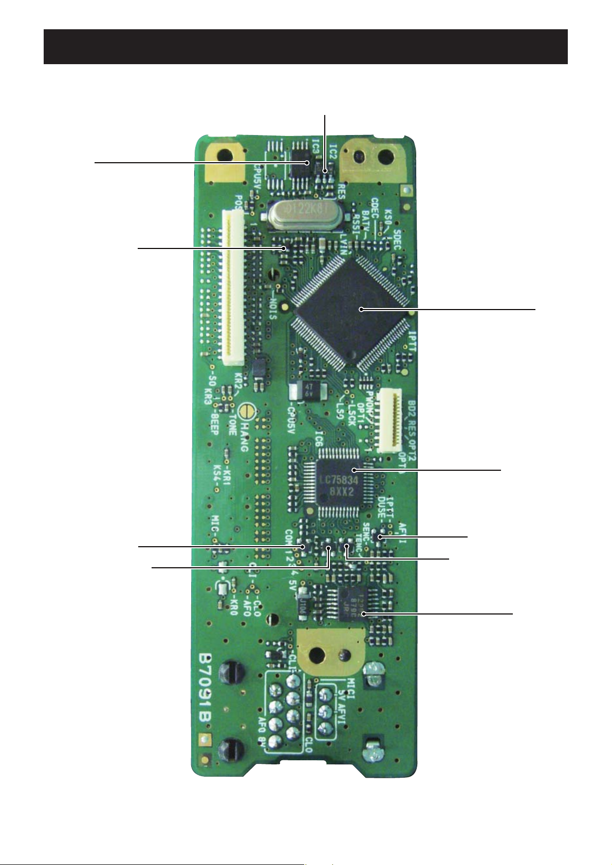
SECTION 2. INSIDE VIEWS
• FRONT UNIT
RESET IC
(IC2)
EEPROM
(IC3)
CLOCK FREQUENCY
SHIFT DIODE
(D6)
BACKLIGHT DRIVER
(Q1)
DIMMER CONTROLLER
(Q2)
CPU
(IC1)
LCD DRIVER
(IC6)
TONE FILTER SWITCH
(Q3)
BACKLIGHT CONTROLLER
(Q5)
2 - 1
TONE LPF
(IC5)
Page 7
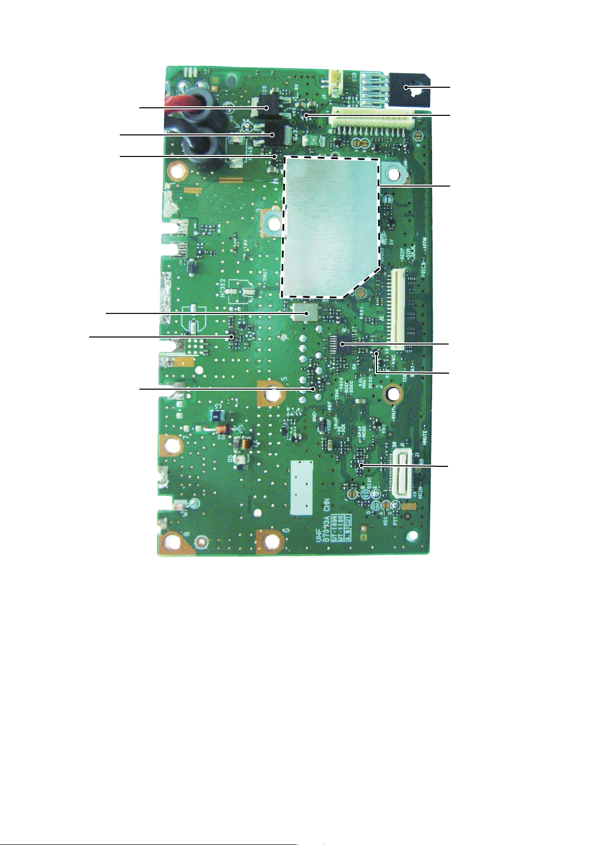
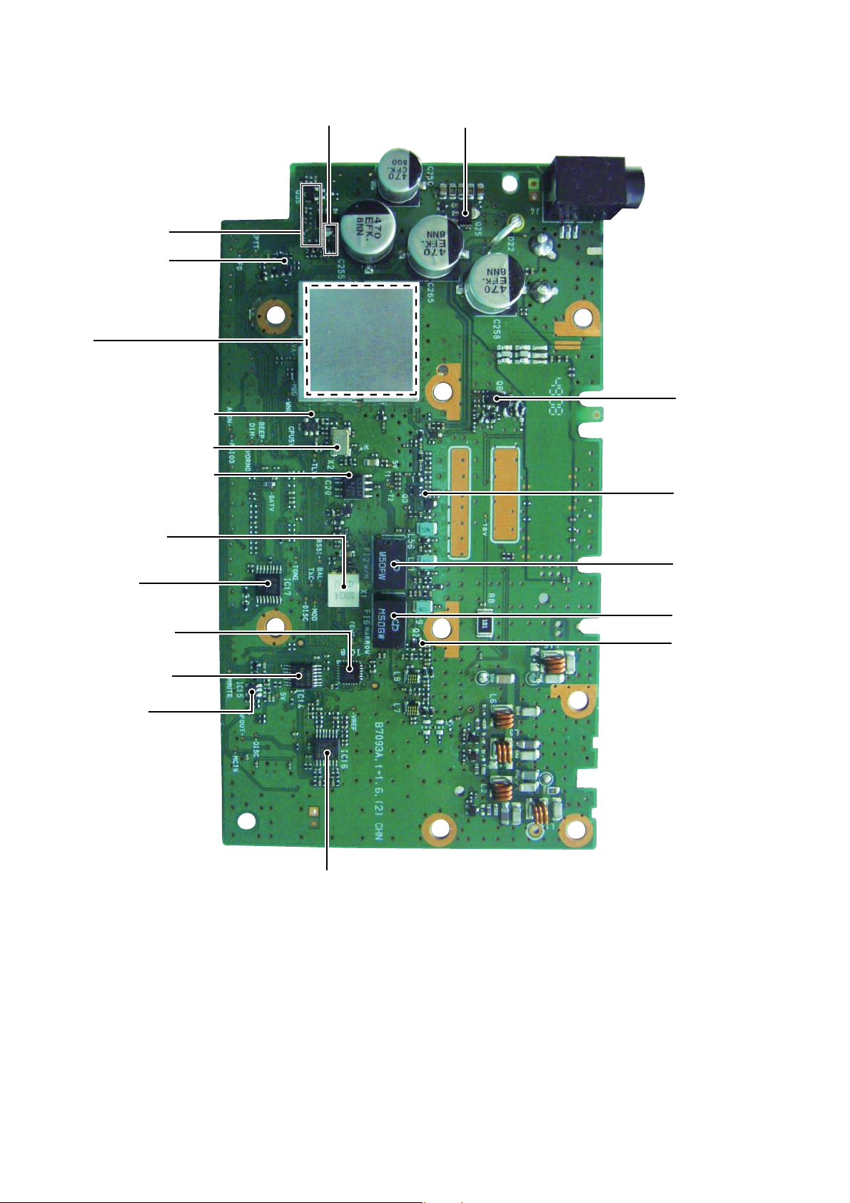
• MAIN-A UNIT
(TOP VIEW)
+8 LINE REGULATOR
POWER SWITCH
(Q23)
POWER SWITCH
(Q24)
(IC9)
AF AMP
(IC8)
CPU5 LINE REGULATOR
(IC10)
PLL CIRCUIT
1ST IF FILTER
(FI1)
APC AMP
(IC2)
2ND IF FILTER SWITCH
(Q40)
IF IC
(IC1)
DISCRIMINATOR SWITCH
(Q5)
LPF
(Q39)
2 - 2
Page 8
• MAIN-A UNIT
(BOTTOM VIEW)
AF MUTE SWITCH
(Q35, Q36)
Ext. MODULATION
LINE SWITCH
(Q31)
VCO
REFERENCE OSCILLATOR
MODULATION AMP
(IC19)
REFERENCE FREQUENCY
OSCILLATOR (X2)
D/A CONVERTER
(IC20)
+5V LINE REGULATOR
(Q27,Q28)
T8 LINE REGULATOR
(Q25)
DRIVE AMP
(Q9)
1ST MIXER
(Q3)
DISCRIMINATOR
(X1)
EXPANDER
(IC17)
D/A CONVERTER
(IC18)
ANALOG SWITCH
(IC14)
AF PRE-AMP
(IC15)
2ND IF FILTER
(FI2)
2ND IF FILTER
(FI6)
RF AMP
(Q2)
AF/TONE FILTERS
(IC16)
2 - 3
Page 9
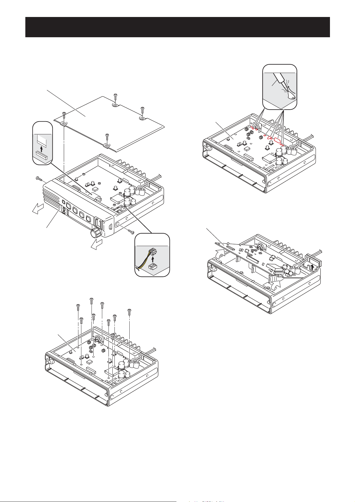
SECTION 3. DISASSEMBLY INSTRUCTION
1) Unscrew 4 screws from the top cover, and remove the top
cover.
2) Disconnect the fl at cable and speaker cable.
3) Unscrew 2 screws from the both sides, and remove the
front panel in the direction of the arrow.
TOP COVER
FLAT
CABLE
5) Unsolder total of 9 points; 3 points at the antenna
connector, 6 points at the PA module.
UNSOLDER
Solder
remover
MAIN UNIT
6) Take off the MAIN UNIT from the CHASSIS.
FRONT PANEL
4) Unscrew 9 screws from the MAIN UNIT.
MAIN UNIT
MAIN UNIT
SPEAKER
CABLE
(Continued to right above)
3 - 1
Page 10
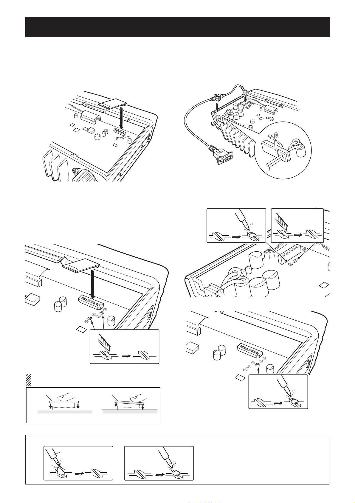
SECTION 4 OPTIONAL PRODUCTS INSTALLATION
Install optional UT-108R as follows;
1) Turn the transceiver power OFF, then disconnect the DC
power cable.
2) Unscrew 4 screws, then remove the bottom cover.
3) Install the unit as shown below.
4) Recover the bottom cover, screws and DC power cable.
Install optional UT-109R or UT-110R as follows;
1) Turn the transceiver power OFF, then disconnect the DC
power cable.
2) Unscrew 4 screws, then remove the bottom cover.
3) Cut the pattern on the PCB at "MIC" and "DISC" as
showon below.
4) Install the unit as shown below.
5) Recover the bottom cover, screws and DC power cable.
Install optional OPC-1939 as follows;
1) Turn the transceiver power OFF, then disconnect the DC
power cable.
2) Unscrew 4 screws, then remove the bottom cover.
3) Install the cable as shown below.
OPC-1939
Cut off the bushing as in the illustration,
when you install the optional OPC-1939.
4) Cut or short the patterns as below. (For AF output)
DISC
MIC
NOTE: When attaching the unit
Be sure that the unit is inserted correctly.
OPTIONAL UNIT
OPTIONAL UNIT
OK
NG
K
I
5) Short the pattern as below. (For modulation input)
D
6) Recover the bottom cover, screws and DC power cable.
NOTE: Be sure to recover the patterns when you remove the optional product. Otherwise no TX modulation or AF output is available.
Solder
remover
4 - 1
Page 11
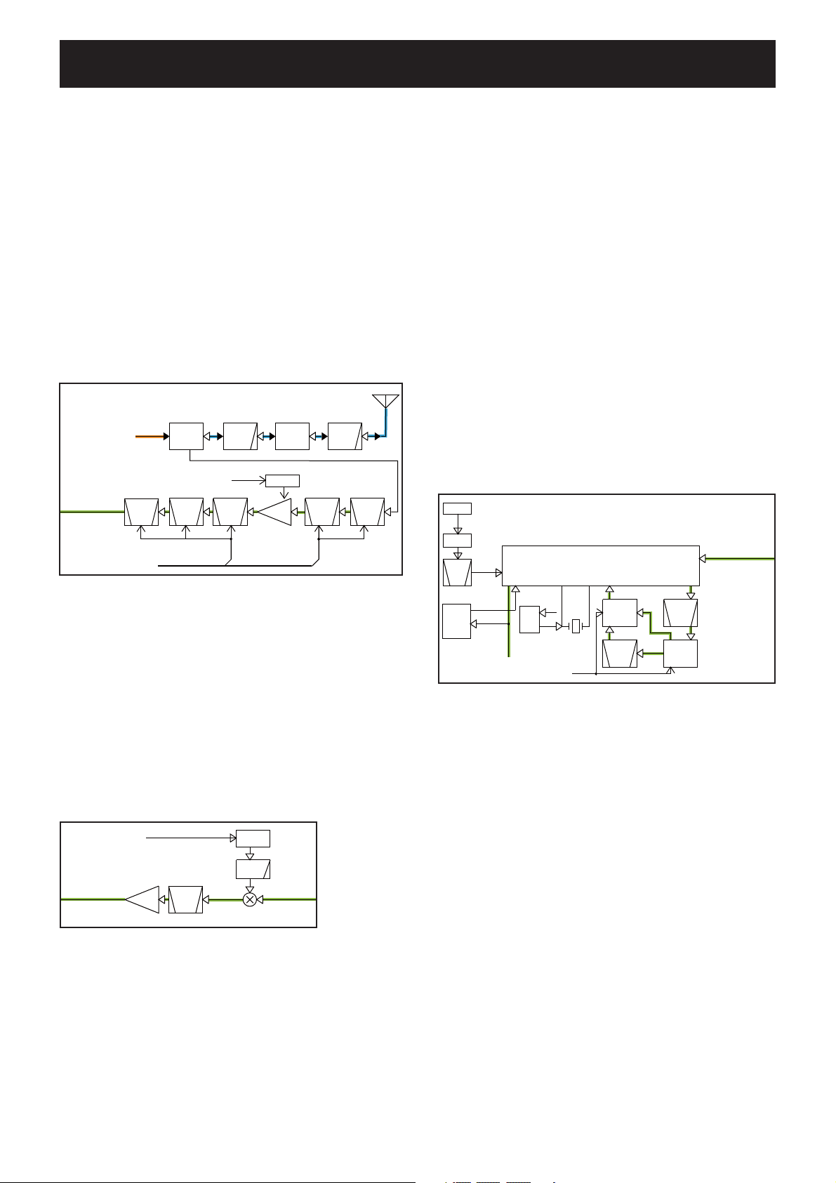
SECTION 5. CIRCUIT DESCRIPTION
t
5-1 RECEIVER CIRCUITS
RF CIRCUITS
RF signals from the antenna are passed through the LPF (as
the harmonic filter for transmitting) and antenna SW, then
applied to the RX BPF circuit.
The applied RX signals are passed through the 2-staged
tuned BPF (D8, 20 and D4, 21) to remove unwanted out-ofband signals, and amplified by the low-noise RF AMP (Q2),
then applied to the 1st mixer (Q3) via three BPFs (D9, 10
and D19).
Each BPF is tuned to the RX frequency by the tuning
voltage “T1” and “T2” from the D/A converter (IC20), to
obtain required IMD characteristic.
• RF CIRCUITS
D3,5,6
From the TX AMP
To 1st IF circuits
D19
BPF
ANT
SW
D10
BPF
D9
BPF
Tuning voltage “T2”
1ST IF CIRCUITS
The RX signals from the BPF are mixed with the 1st LO
signals to be converted into the 46.35 MHz 1st IF signal.
The 1st LO signals are generated by the RX VCO (Q14,
D33, 62, 63), and passed through the LO SW (D15) and
attenuator, then applied to the 1st mixer (Q3)
RSSI
Q1
Q2
D1,11,12
PWR
DET
AGC
RF
AMP
LPFLPF
D4,21
D8,20
BPF
BPF
Tuning voltage “T1”
2ND IF AND DEMODULATOR CIRCUITS
The amplified 1st IF signal is mixed with the 2nd LO signal
at the internal 2nd IF mixer of the IF IC (IC1), to obtain the
450 kHz 2nd IF signal.
The 15.3 MHz signal generated by the reference oscillator
(X2) is passed through the filter AMP (Q34) to extract the
45.9 MHz 3rd harmonic component. The 45.9 MHz signal is
then applied to pin 2 of IF IC (IC1) as the 2nd LO signal.
The converted 2nd IF signal is output from pin 3 of IF IC
(IC1), and filtered by the ceramic filters (FI2 and FI6 for
Narrow mode; FI2 only for Wide mode) to remove unwanted
out-of-band signals, then applied to the internal frequencydemodulator of IF IC (IC1) from pin 5.
The demodulator is a quadrature type which uses X1 as the
phase shifter.
The frequency-demodulated AF signals are output from pin 9
to AF circuits.
• 2ND IF AND DEMODULATORCIRCUITS
X2
REF
15.3MHz
X3
Q34
BPF
D/A
IC18
AK2330
IC1:TA31136FN
45.9MHz
SQIN
DISC
To the AF circuits
IF IC
Q5
NWC
W/N
SW
D57
W/N
X1
SW
FI6
450kHz
CERAMIC
BPF
NWC
FI2
CERAMIC
BPF
D56
W/N
SW
From 1st IF circuits
The converted 1st IF signal is filtered by the crystal filter (FI1)
and amplified by the 1st IF AMP (Q4), then applied to the IF
IC (IC1).
• 1ST IF CIRCUITS
To IF IC
1st LO signals
(182.35 MHz-220.35 MHz)
Q4
IF
AMP
FI1
XTAL
BPF
D14,15
46.35 MHz
1st mixer
To 1st IF circuits
TX/RX
SW
LPF
Q3
From RF circui
5 - 1
Page 12
AF CIRCUITS
The demodulated AF signals from the IF IC (IC1) are
amplified and filtered by the HPF (IC16), and passed
through the AF line SW (IC14) and LPF (IC16). The filtered
AF signals are adjusted its level (=loudness) by the D/A
converter (IC18), and applied to the AF AMP (IC15) via the
AF line SW (IC14).
SIGNALING (DECODING)
Demodulated signals from pin 9 of the IF IC (IC1) are
passed through the LPF to extract tone signals contained in
the demodulated signals.
2/5 tone signals are extracted by the LPF (IC16). CTCSS/
DTCS signals are extracted by the LPF (Q39).
The amplified AF signals are applied to the AF power AMP
(IC8) and power-amplified to obtain AF output level.
The power-amplified AF signals are applied to the internal
speaker on the FRONT UNIT or output from the external
speaker jack on the rear panel.
• RX AF CIRCUITS
From the IF IC
DISC
DISC
DISC
IC16
RXAF
HPF
IC16
LPF
(2/5 TONE signals)
Q39
LPF
(TCSS/DTCS signals)
D/A
IC18
AK2330
SDEC
CDEC
IC14
CD4066
ANALOG
VRAF
To CPU (FRONT UNIT: IC1)
IC16
LPF
SW
TMONI
IC15
AF
AMP
AF ON
AF
MUTE
Q35,36,D29
FRONT UNIT
These extracted tone signals are applied to the CPU (FRONT
UNIT: IC1) for decoding.
AF
POWER
AMP
IC8
LA4425A
J4
Ext. speaker jack
Int. speaker
5 - 2
Page 13
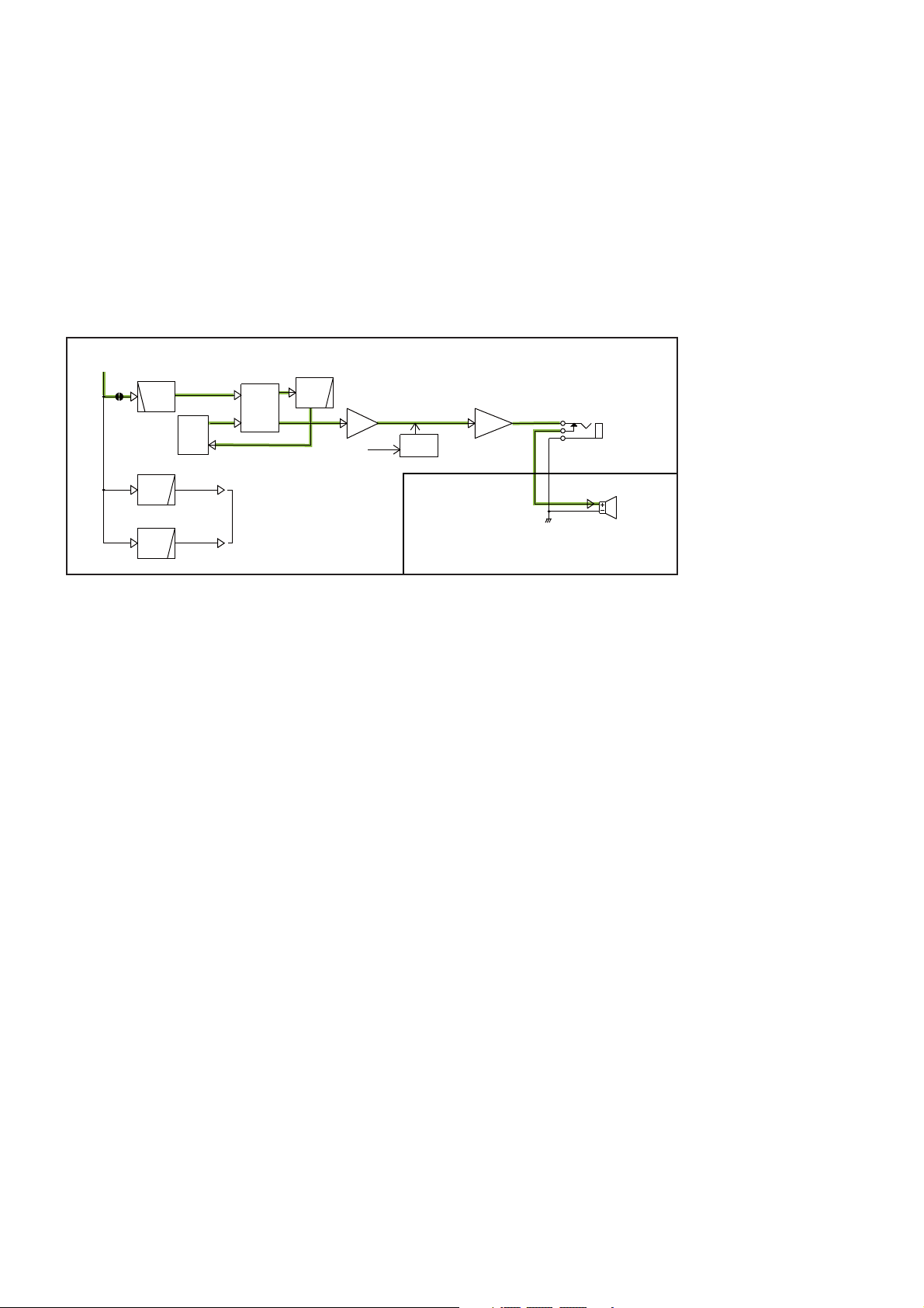
5-2 TRANSMITTER CIRCUITS
MIC AMPLIFIER (FRONT UNIT)
Audio signals from the connected microphone are applied to
the MIC AMP (IC5) via the microphone connector (J1). The
amplifi ed MIC signals are applied to the MAIN UNIT.
CTCSS/DTCS SIGNALS ENCODING (FRONT UNIT)
The CTCSS/DTCS encoding signals from the CPU (IC1)
“CENC0–CENC2” are passed through the LPF (IC5) for
waveform conversion, and applied to the MAIN UNIT as tone
modulation signals.
TX AF CIRCUITS
The MIC signals from the FRONT UNIT are passed through
the D/A converter (as a MIC gain controller; IC18) for level
adjustment, and applied to the limiter AMP which is also
rolled to the pre-emphasis circuit (IC16).
• TX AF CIRCUITS
To the Reference
frequency oscillator
MCOT
D/A
MCGO
BAL
IC18
AK2330
HPF
MODI
IC16
Limiter
Pre-empha.
MIC
line
SW
IC14
CD4066
SPIN
MODVRAF
IC16
TX VCO
Splat.
MIC
TONE
CDTS
MIC
J1
MICROPHONE
CONNECTOR
IC5
AMP
FRONT UNIT
MIC MUTE SWITCH
The pre-emphasized MIC signals are passed through the
MIC mute SW (IC14).
While receiving, the MIC mute SW (IC14) cuts the MIC line
off, and is controlled by “MMUT” signal from the expander
(IC17).
2/5 TONE, DTMF ENCODING (FRONT UNIT)
Encoding signal from the CPU (IC1) named “SENC” is
passed through the LPF (IC5), and applied to the MAIN
UNIT as tone modulation signals.
TX AMPLIFIERS
The frequency-modulated signal from the TX VCO is bufferamplifi ed by two buffers (Q11 and Q10), and applied to the
YGR AMP (Q9) as the TX signal via the LO SW (D14).
The amplifi ed TX signal is amplifi ed by the drive AMP (Q8),
and applied to the FET HPA module (IC3) via the LPF, and
power-amplifi ed to obtain TX output power level.
The power-amplified TX signal is passed through the
antenna SW (D3) and LPF as a harmonic filter, then fed to
the antenna.
APC CIRCUIT
A portion of TX signal rectifi ed by D1, D11 and D12 on the
TX line to detect TX power level. The rectified voltage is
applied to the APC AMP (IC2), and the APC AMP controls
the gain of HPA module (IC3) automatically by comparing
the rectifi ed voltage and the power setting voltage "T1."
SPLATTER FILTER
The MIC signals from the MIC mute SW (IC14) are applied
to the splatter fi lter (IC16).
The splatter filter (IC16) is also used as the AF Summing
AMP for tone signals modulation (CTCSS, 2/5 TONE).
MODULATION CIRCUIT
MIC signals from the splatter filter (IC16) is level-adjusted
(=deviation adjustment) by the D/A converter (IC18), and
applied to the TX VCO (Q13, D16, 64, 65) via modulation
mute SW (IC14) as the modulation signals.
The MIC signals are also applied to the reference frequency
oscillator (X2) as the modulation signals via D/A converter
(IC18) and REF AMP (IC19).
• MODULATION CIRCUITS
D14,D15
Q10
TX VCO
Q11
BUFF
BUFF
TX/RX
SW
To TX AMPs
X2
IC4
CR-794
IC19
BAL
REF
AMP
REF
OSC
15.3 MHz
MB15A02
IC
LOOPPLL
FIL
LV
Q13,D16,64,65
D18
FM
MOD
• TX AMPLIFIERS APC CIRCUIT
Q9
YGR
AMP
From TX VCO
Q8
DRIVE
AM
IC
3
P
PWR
AMP
D3
ANT
SW
RX circuits
D1,11,D12
DET
LPFLPF LPFLPF
PWR
IC2
APC
AMP
T1
MUTE
Q6
SW
TMUT
From the D/A converter
From the TX AF circuits
5 - 3
Page 14
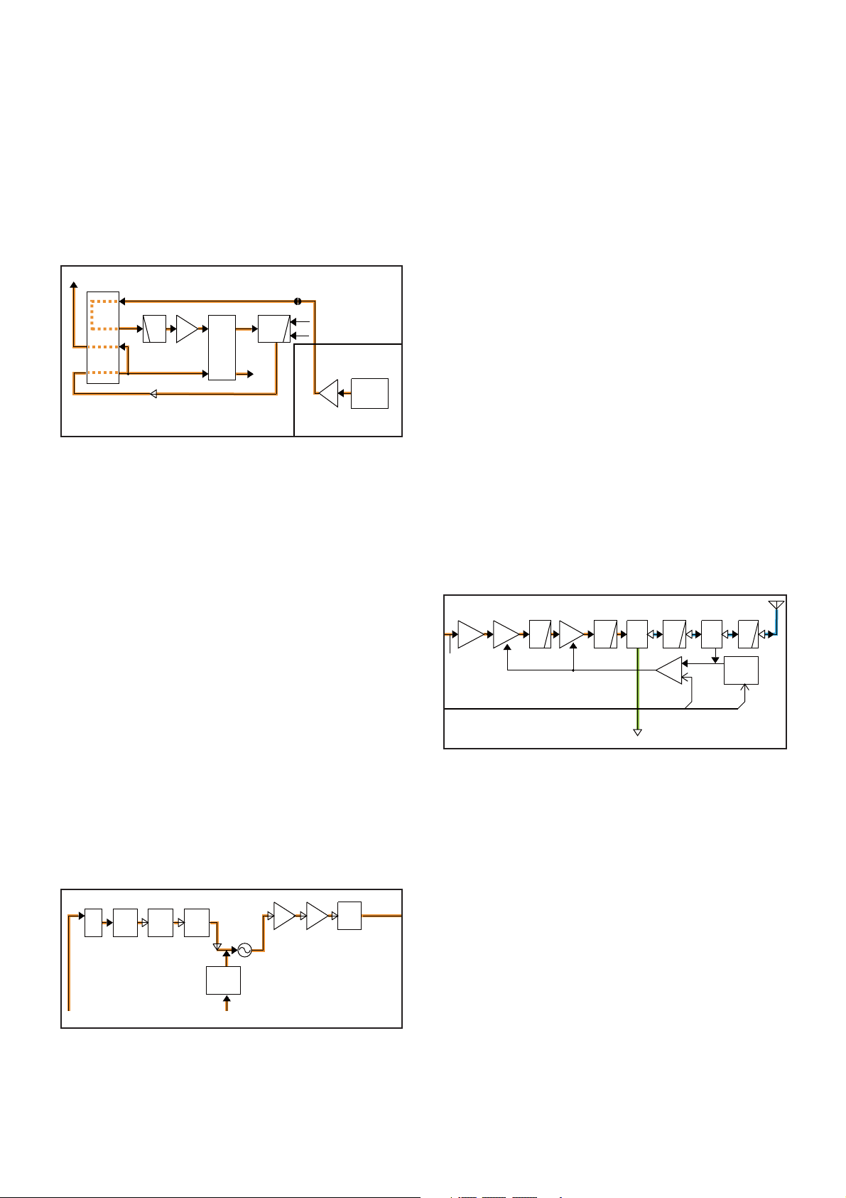
5-3 FREQUENCY SYNTHSIZER CIRCUITS
VCOs
The TX VCO which generates TX signal is composed by
Q13, D16, 64 and 65, and the frequency modulation is
carried out by applying modulation signals to D18.
The RX VCO which generates 1st LO signals is composed
by Q14, D33, 62 and 63.
These two VCOs are switched by the VCO SW (Q15, 16)
using “RXC” signal.
The output signals from each VCO are amplified by the
buffer AMP (Q11) and LO AMP (Q10), then applied to the
TX or RX circuits.
A portion of oscllated signals is applied to the PLL IC (IC4)
via the dubler (Q12) and Lo fi lters (BPF and LPF).
PLL
The applied VCO output is divided according to the serial
data including divide ratio from the CPU, at the prescaler
and programmable divider. In the same way, the reference
frequency signal from the reference frequency signal
oscillator is applied to the PLL IC and divide so that these
are the same frequency.
The frequency-matched signals are applied to the phase
comparator and phase-compared. The resulted phase
difference is detected as a phase-type signal, and leveladjusted at the charge pump then output. The output pulse
type signal is passed through the loop filter to be converted
into the DC voltage (=Lock Voltage).
Applying the lock voltage to the variable capacitors
(VD) which composes a part of the resonator of VCO,
the capacitance of VDs changes corresponding to the
applied lock voltage. This causes the change of resonation
frequency that determines the VCO oscillating frequency to
keep the VCO frequency constant.
When the oscillation frequency drifts, its phase changes
from that of the reference frequency, causing a lock voltage
change to compensate for the drift in the VCO oscillating
frequency.
• FREQUENCY SYNTHESIZER CIRCUITS
8V
REF
IC19
Q17
RIPPLE
FIL
D52
RLVA
RLV
TLVA
AD J
D53
TLV
AD J
From the TX AF circuits
X2
CR-794
AMP
REF
Q34
X3
BPF
15.3MHz
45.9MHz
IC4
MB15A02
IC
Clock,Data,Strobe
LPF
IF IC
IC1:TA31136FN
LOOPPLL
FIL
BPF
Q14
D33,62,53
RX VCO
LVLV
Q13
D16,64,65
TX VCO
D18
FM
MOD
Q15,16
Q12
VCO
RXC
SW
TXC
Q11
BUFF
X2
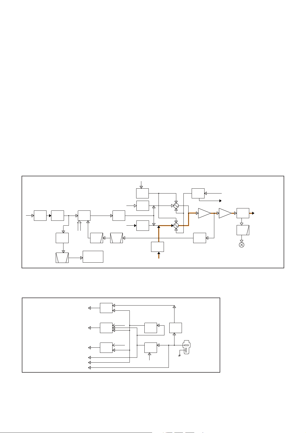
5-4 VOLTAGE BLOCK DIAGRAM
Voltage from the power supply is routed to the whole of the transceiver via regulators and switches.
Q27
IF IC (IC1), PLL IC(IC4), etc.
YGR(Q9), Driver(Q8), APC AMP(IC2), etc.
Q28
+5
5V
REG
8V
Q29
Q25
D23
T8V
TMUT
T8
VCC
REG
8V
IC9
REG
CPU5CPU5
+8
CPU5
REG
IC10
Q10
LO AMP
D14,D15
TX/RX
SW
LPF
Q3
1st IF mixer
TX amplifiers
RF AMP(Q2), 1st IF AMP(Q4), 1st mixer(Q3), etc.
External output(from J6)
VCOs, FRONT UNIT
HPA module(IC3)
Q30
Q26
R8V
VCC
8V
HV
RXC
R8
REG
8V
Q24
Q23
POWER
SW
PWON
HV
Power supply cable
W2
5 - 4
Page 15

5-5 PORT ALLOCATIONS
5-5-1 CPU (FRONT UNIT; IC1)
Pin
Port
No.
Name
KR1−
1−3
4−8
10 CCS
19−21CENC0−
CENC2
23 DUSE
24 IPTT
25 HANG
30 PLST
34 ULCK
39 DSDA
43 SENC
44 BEEP
45 SDEC Input port for DTMF signals.
46 CDEC Input port for CTCSS/DTCS signals.
48 BATV Input port for power supply voltage.
49 LVIN Input port for VCO lock voltage.
50 RSSI
51 TEMP
52 AFVI
59 RES
69 CSFT
71 DAST
IGSW/
72
75 NOIS
79 CLO Cloning data output.
80 CLI Cloning data input.
82 ESDA
85 ESCL
86 PWON
91 LSO
92 LSCK
93 LCS
94 LINH
95 LIGT2
Input ports for dealer-programmable keys.
KR3
KS0−
Output ports for dealer-programmable keys.
KS4
Outputs chip-select signal to the attached optional
unit.
Output ports for CTCSS/DTCS signal.
Frequency response of tone filter (FRONT UNIT;
IC5) switching signal.
“Low”=While transmitting.
PTT input from connected microphone.
“Low”=PTT is pushed.
Microphone on/off hook detect.
“Low”=The microphone is off hook.
Outputs PLL strobe signal to the PLL IC (MAIN UNIT;
IC4, pin 11).
Input port for PLL unlock detect signal from the
PLL IC (MAIN UNIT; IC4, pin 7).
“Low”=While the PLL circuit is unlocked.
Outputs serial data to the D/A converter (MAIN
UNIT; IC20, pin 6).
Outputs DTMF signals to the LPF (FRONT UNIT;
IC5, pin 3).
Outputs beep sounds to the LPF (FRONT UNIT;
IC5, pin 7).
Input port for receive signal strength level signal
from the IF IC (MAIN UNIT; IC1, pin 12).
Voltage divided by thermal register (MAIN UNIT;
R209) and R210. (temperature monitor)
[VOL] dial (FRONT UNIT; R14) input. (divided
voltage of 5V line)
Input port for CPU reset signal from the reset IC
(FRONT UNIT; IC2, pin 1).
“Low”=When the CPU is reset.
Outputs CPU clock shift signal to the clock
frequency shift switch (FRONT UNIT; D6).
Outputs strobe signal to the D/A converter (MAIN
UNIT; IC18, pin 7).
• Ignition SW control input.
Or
DIM
• Dimmer control input.
Input port for noise signal from the IF IC (
IC1, pin 13).
Outputs serial data to the EEPROM (FRONT UNIT;
IC3, pin 5).
Outputs clock signal to the EEPROM (FRONT
UNIT; IC3, pin 6).
Transceiver's power control.
“High”=Power ON.
Outputs serial data to the LCD driver (FRONT UNIT;
IC6, pin 48).
Outputs clock signal to the LCD driver (FRONT UNIT;
IC6, pin 47).
Outputs chip-enable signal to the LCD driver
(FRONT UNIT; IC6, pin 46).
Outputs display inhibit signal to the LCD driver
(FRONT UNIT; IC6, pin 45).
Outputs LCD backlight control signal to the
backlight LEDs (FRONT UNIT; DS1–9) driver
(FRONT UNIT; Q5).
“High”=While the backlight is ON.
Description
MAIN UNIT;
Pin
Port
No.
Name
98 SCK
99 SO
100 KR0 Input ports for dealer-programmable keys.
Outputs serial clock signal to the PLL IC (IC4,
pin 9) and D/A converters (IC17, pin 3/IC18, pin 8/
IC20, pin 7).
Outputs serial data to the PLL IC (IC4, pin 9) and D/
A converters (IC17, pin 3/IC18, pin 8/IC20, pin 7).
Description
5-5-2 EXPANDER (MAIN UNIT; IC17)
Pin
No.
Line
Name
1 EXST Strobe (load enable) input.
2 SO Serial data input.
3 SCK Serial clock input.
4 RXC T8V, R8V lines and RX VCO ON/OFF control.
5 AFON
6 NWC
7 RMUT
12 HORNO
13 TMUT
AF mute SW (Q35) control.
“Low”=Mute
• RX band width switching signal to the 2nd IF
fi lter SW (D56, 57).
“Low”=Narrow mode
• RX band width switching signal to the phase
shifter SW (Q5).
“Low”=Wide mode
Outputs AF mute signal to the analog switch
(IC3, pins 12, 13).
“Low”=While the squelch is close or transmitting.
External device control.
“Low”=Pin 6 of OPC-1939 (if connected) is “Low.”
Outputs transmit mute signal to the transmit
mute switch (Q46).
“High”=Transmitting is muted.
Description
5-5-3 D/A CONVERTER (MAIN UNIT; IC18)
Pin
No.
2, 3 MIC signal level adjustment.
4, 5 RX AF/MIC signal level adjustment.
16, 17 Tone signal level adjustment.
Oscillation frequency control voltage to the reference
18, 19
frequency oscillator (X2).
20, 21 Modulation signal level adjustment.
22, 23 Beep sound loudness adjustment.
24, 25 Squelch threshold level adjustment.
Description
5-5-4 D/A CONVERTER (MAIN UNIT; IC20)
Pin
Line
No.
Name
1T1
2T2
3TLVA
4RLVA
• While receiving
Tuning voltage to the tuned BPFs (D4, 21
and D8, 20).
• While transmitting
TX power level setting signal to the APC AMP
IC2).
Tuning voltage to the tuned BPFs (D9, D10 and
D19).
Oscillation frequency correcting voltage to the TX
VCO (Q13, D16, 53, 64, 65).
Oscillation frequency correcting voltage to the RX
VCO (Q14, D33, 52, 62, 63).
Description
5 - 5
Page 16

SECTION 6. ADJUSTMENT PROCEDURE
6-1 PREPARATION
REQUIRED EQUIPMENTS
M
EQUIPMENT GRADE AND RANGE EQUIPMENT GRADE AND RANGE
Cloning Software
DC Power Supply
Modulation
Analyzer
Frequency Counter
RF Power Meter
JIG CABLE
M
CS-F5020 : Revision 1.0 or later
Output voltage
Current capacity
Frequency range
Measuring range
Frequency range
Frequency accuracy
Sensitivity
Measuring range
Frequency range
Impedance
SWR
: 13.6 V DC except [EUR]
13.2 V DC [EUR]
: 15 A except [EUR]
10 A [EUR]
: DC–600 MHz
: 0 to ±10 kHz
: 0.1–600 MHz
: ±1 ppm or better
: 100 mV or better
: 0.1–30 W [25 W ver.]
0.1–60 W [45 W ver.]
: 100–600 MHz
: 50
Ω
: Better than 1.2 : 1
JIG Cable
Attenuator
External Speaker
Standard Signal
Generator (SSG)
Oscilloscope
Modifi ed OPC-1122U
(see the illust below)
Power attenuation
Capacity
Input impedance
Capacity
Frequency range
Output level
Frequency rang
Measuring range
: 40 or 50 dB
: 30 W [25 W ver.]
60 W [45 W ver.]
: 4
: 5 W or more
: 0.1–600 MHz
: –20 to 90 dBµ
: DC–20 MHz
: 0.01–20 V
Ω
(–127 to –17 dBm)
OPC-1122U (USB type Cloning cable)
GND
SP
GND
MIC
GND
PTT
Add a jumper wire here
EXT. SPEAKER
(5 W/4 Ω)
+−
+
4.7 µF
PTT SWITCH
AUDIO GENERATOR
(300–3000 Hz/1–500 mV)
+−
AC MILLIVOLTMETER
SETTING;
Frequency : 1 kHz
Level : 40 mVrms
Waveform : Sine wave
(10 mV to 10 V)
+−
6 - 1
Page 17

ADJUSTMENT FREQUENCIES
Select “Middle”
M
Before starting adjustment, clone adjustment frequencies and settings into the transceiver as below.
• For [Low band] version (400–470 MHz)
• For [High band] version (450–512/520 MHz)
NOTE: FOR [F6022], when adjust “Deviation,” “Modulation Balance,” “RX SENSITIVITY”
and “S-meter” in the middle mode, change the bandwidth to “Middle” as below.
6 - 2
Page 18

CONNECTION
M
Oscilloscope
Standard signal generator
–90 to +90 dBµ
(–127 to –17 dBm)
CAUTION:
DO NOT transmit while
SSG is connected to
the antenna connector.
to USB port
AC millivoltmeter
Audio generator
PC
Modulation analyzer
(DC measurable)
Attenuator
40 dB or 50 dB
13.6 V / 15 A except [EUR]
13.2 V / 10 A [EUR]
JIG CABLE
RF power meter
30 W [25 W ver.]
60 W [50 W ver.]
DC power supply
to the MIC
connector
Frequency
counter
to the antenna connector
to DC cable
ADJUSTMENT UTILITY WINDOW (example)
M
Click to open the
“I/O Check window”
ADJ. CHANNEL
TX POWER
MOD. BALANCE
DEVIATION
CTCSS\DTCS
SQUELCH
REF. FREQUENCY
RX SENSITIVITY
LOCK VOLTAGE
RSSI
(S3 and S1 level)
6 - 3
Page 19

6-2 FREQUENCY ADJUSTMENT
1) Select an adjustment item using cursor or [↑] / [↓] of the PC’s keyboard.
2) Set or modify the adjustment value as specifi ed using [←] / [→] of the PC’s keyboard, then push [ENTER].
ADJUSTMENT ADJUSTMENT CONDITION OPERATION VALUE
PLL LOCK
VO LTAGE
-adjustment[RX LVA]
[TX LVA] 2 • Channel
PLL LOCK
VO LTAGE
-verifi cation-
REFERENCE
FREQUENCY
[REF]
1 • Channel
• Receiving
• Transmitting
1 • Channel
• Receiving
2 • Channel
• Transmitting
1 • Channel : 1-3
• Connect an RF power meter to the
antenna connector.
• Transmitting
: 1-1 Select the item [RX LVA], then adjust the
: 1-1 Select the item [TX LVA], then adjust the
: 1-2 Click [Reload (F5)] button, then check the
: 1-2 2.8–3.8 V
• I/O Check window
voltage (LVIN) using [←] / [→] of the PC’s
keyboard.
voltage (LVIN) using [←] / [→] of the PC’s
keyboard.
“LVIN” item on the “I/O Check window.”
Loosely couple a frequency counter to the
antenna connector.
3.2–4.2 V
470.000000 MHz
[Low band]
520.000000 MHz
[High band]
1.3 V
1.5 V
Lock voltage
(The values shown in the above screen are example only.
Each transceiver has their own values.)
6 - 4
Page 20

6-3 TRANSMIT ADJUSTMENT
1) Select an adjustment item using cursor or [↑] / [↓] of the PC’s keyboard.
2) Set or modify the adjustment value as specifi ed using [←] / [→] of the PC’s keyboard, then push [ENTER].
ADJUSTMENT ADJUSTMENT CONDITION OPERATION VALUE
OUTPUT
POWER
[Power (Hi)]
[Power (L2)] 2 • Channel : 1-5
[Power (L1)] 3 • Channel : 1-6
MODULATION
BALANCE
[BAL]
DEVIATION
-PREPARATION -
(NARROW)
[MOD N]
(WIDE)
[MOD Ratio]
(MIDDLE)*
[MOD Ratio]
CTCSS/DTCS
DEVIATION
[CTCSS/DTCS]
*: [EUR] only
1 • Channel : 1-4
• Transmitting
• Transmitting
• Transmitting
1 • Channel : 1-7
• No audio signals applied to the JIG cable.
• Set a modulation analyzer as;
HPF : OFF
LPF : 20 kHz
De-emphasis : OFF
Detector : (P–P)/2
• Transmitting.
• Connect an audio generator to the JIG
1
cable and set as;
Frequency : 1.0 kHz
Level : 40 mVrms
• Set the modulation analyzer to the
same condition as “MODULATION BAL-
ANCE.”
• Channel : 1-8
2
• Transmitting
• Channel : 1-9
3
• Transmitting
• Channel : 1-10
4
• Transmitting
• Channel : 1-11
1
• No audio signals applied to the JIG cable.
• Set the modulation analyzer to the
same condition as “MODULATION BAL-
ANCE.”
• Transmitting
Connect an RF power meter to the antenna connector.
Connect the modulation analyzer with
an oscilloscope to the antenna connector through an attenuator.
Connect a modulation analyzer with an
oscilloscope to the antenna connector
through an attenuator.
Connect a modulation analyzer with an
oscilloscope to the antenna connector
through an attenuator.
[25W ver.]
[45 W ver.]
[25W ver.]
[45 W ver.]
[25W ver.]
[45 W ver.]
Set to square
±2.05 to ±2.15 kHz
±4.05 to ±4.15 kHz
±3.25 to ±3.35 kHz
±0.65 to ±0.75 kHz
25 W
45 W
10 W
25 W
2.5 W
4.5 W
waveform
–
6 - 5
Page 21

6-4 RECEIVE ADJUSTMENT
1) Select an adjustment item using cursor or [↑] / [↓] of the PC’s keyboard.
2) Set or modify the adjustment value as specifi ed using [←] / [→] of the PC’s keyboard, then push [ENTER].
ADJUSTMENT ADJUSTMENT CONDITION OPERATION VALUE
RECEIVE
SENSITIVITY
[BPF T1]
[BPF T2]
NOTE: When
1
• Channel : 1-12
• Receiving
• Connect an SSG to the antenna connector and set it as;
Frequency :
: 450.100 MHz
Level : +20 dBµ† (–87 dBm)
Modulation : 1 kHz
Deviation : ±3.0 kHz except [EUR]
±2.4 kHz [EUR]
S-METER
[RSSI]
(S3 level)
NOTE: "RECEIVE SENSITIVITY" MUST be adjusted before "S-METER." When "RECEIVE SENSITIVITY" is re-
adjusted, "S-METER" MUST be re-adjusted too.
1
• Channel : 1-13
• Connect an SSG to the antenna connector and set it as;
Frequency :
: 450.100 MHz
Level : +23 dBµ† (–84 dBm)
Modulation : 1 kHz
Deviation : ±3.0 kHz except [EUR]
±2.4 kHz [EUR]
• Receiving
(S1 level)
2
• Set the SSG as;
Level : –7 dBµ
• Receiving
SQUELCH
[SQL]
1 • Channel : 1-14
• Connect an SSG to the antenna connector and set it as;
Frequency :
: 450.100 MHz
Level : –13 dBµ† (–120 dBm)
Modulation : 1 kHz
Deviation : ±3.0 kHz
• Receiving
†
; The output level of the standard signal generator (SSG) is indicated as the SSG’s open circuit.
“RECEIVE SENSITIVITY” is re-adjusted, “S-METER” must be re-adjusted too.
1) Select the item [BPF T1] then push
[ENTER].
2) Select the item [BPF T2] then push
[ENTER].
400.100 MHz [Low band]
[High band]
Select the item [RSSI S3 Level], then
push [ENTER] to store the adjust value
for S3 level.
400.100 MHz [Low band]
[High band]
†
(–114 dBm)
Select the item [RSSI S1 Level], then
push [ENTER], to store the adjust value
for S1 level.
1) Once close the squelch by increasing
[SQL] value, then decrease the value
to open the squelch.
400.100 MHz [Low band]
2) Push [ENTER] to store the value.
[High band]
(Automatic
adjustment)
(Automatic
adjustment)
(Automatic
adjustment)
6 - 6
Page 22

SECTION 7. PARTS LIST
[MAIN-A UNIT]
REF PARTS
NO. NO.
IC1 1110003491 S.IC TA31136FNG(D,EL) T 57.8/24.7
IC2 1110002751 S.IC TA75S01F(TE85R,F) T 60/54.9
IC3 1150002380 IC RA30H4047M1-101 [EUR-01]
1150002380 IC RA30H4047M1-101 [EXP-01]
1150002400 IC RA60H4047M1-121 [USA-01]
1150002400 IC RA60H4047M1-121 [EXP-03]
1150002400 IC RA60H4047M1-121 [CHN-01]
IC4 1140005991 S.IC MB15A02PFV1-G-BND-ERE1 T 77.8/29.2
IC8 1110003091 IC LA4425A-E
IC9 1180003500 S.REG NJM7808DL1A-TE1-#FZZB T 123.3/45.7
IC10 1180003460 S.REG NJM2831F05-TE1-#ZZZB T 121.6/35.4
IC14 1130011770 S.IC CD4066BPWR B 35.1/16.4
IC15 1110002751 S.IC TA75S01F(TE85R,F) B 32/6.7
IC16 1110005340 S.IC NJM12902V-TE1-#ZZZB B 20.6/21.1
IC17 1130011760 S.IC CD4094BPWR B 53.1/9.9
IC18 1110007290 S.IC AK2330P-L B 35.9/25.7
IC19 1110002751 S.IC TA75S01F(TE85R,F) B 83.7/18.1
IC20 1190001340 S.IC M62334FP 600C B 72.3/26.3
Q1 1560000841 S.FET 2SK1829(TE85R,F) T 34.6/40.4
Q2 1580000731 S.FET 3SK293(TE85L,F) B 41.5/38.7
Q3 1580000731 S.FET 3SK293(TE85L,F) B 71.4/38.4
Q4 1530002601 S.TRA 2SC4215-O(TE85R,F) T 64.5/25.3
Q5 1590000430 S.TRA DTC144EUA T106 T 55.9/16.1
Q6 1590000430 S.TRA DTC144EUA T106 T 62.6/52.1
Q8 1530002680 S.TRA 2SC3357-T1 B 90.4/52.8
Q9 1530003260 S.TRA 2SC5006-T1 B 84.9/51.5
Q10 1530003311 S.TRA 2SC5107-O(TE85R,F) B 92.8/33.1
Q11 1530003311 S.TRA 2SC5107-O(TE85R,F) B 100.5/31.7
Q12 1530004110 S.TRA MT3S37T(TE85L,F) B 97.6/30.4
Q13 1530002920 S.TRA 2SC4226-T1 R25 B 105.2/30.9
Q14 1530002920 S.TRA 2SC4226-T1 R25 B 98.3/24.2
Q15 1590001400 S.TRA XP1214(TX) T 101/34.4
Q16 1590000430 S.TRA DTC144EUA T106 T 103.5/36.6
Q17 1530002851 S.TRA 2SC4116-BL(TE85R,F) T 107.7/33.8
Q18 1560000541 S.FET 2SK880-Y(T5RICOM,F) T 78/24.5
Q19 1590000430 S.TRA DTC144EUA T106 T 91.8/11.7
Q20 1530002851 S.TRA 2SC4116-BL(TE85R,F) [USA-01] T 60/49.8
1530002851 S.TRA 2SC4116-BL(TE85R,F) [EXP-03]
1530002851 S.TRA 2SC4116-BL(TE85R,F) [CHN-01]
Q23 1550000190 S.FET 2SJ506STR-E T 115.3/45.4
Q24 1590000430 S.TRA DTC144EUA T106 T 110.5/44.3
Q25 1540000550 S.TRA 2SD1664 T100Q B 125.1/47.6
Q26 1510000920 S.TRA 2SA1577 T106 Q T 107.7/44.3
Q27 1520000450 S.TRA 2SB1132 T100 Q B 123.5/21.1
Q28 1590001190 S.TRA XP6501-(TX).AB B 118.7/22.2
Q29 1590003391 S.TRA UNR9215G0L B 126.4/43.3
Q30 1590000430 S.TRA DTC144EUA T106 T 107.7/39.4
Q31 1590001451 S.FET 2SJ144-GR (TE85R,F) B 114.3/13.1
Q33 1590000430 S.TRA DTC144EUA T106 T 113.6/26.6
Q34 1530002851 S.TRA 2SC4116-BL(TE85R,F) B 67.6/25.1
Q35 1590000990 S.TRA DTC363EK T146 B 128.9/17.8
Q36 1590000430 S.TRA DTC144EUA T106 B 118.7/18.3
Q37 1590000430 S.TRA DTC144EUA T106 T 112.3/15.8
Q39 1590001650 S.TRA XP4601(TX) T 25.2/19.5
Q40 1590003381 S.TRA UNR9111G0L T 46.8/33
Q43 1590000680 S.TRA DTC114EUA T106 T 36.4/15.2
Q44 1590000430 S.TRA DTC144EUA T106 T 53/14.3
D1 1790001211 S.DIO 1SS375-TL-E B 19.2/49.9
D3 1710001061 DIO L407CDB
D4 1750000711 S.VAR HVC350BTRF-E B 36/40.2
D5 1750001360 S.DIO L709CER (9401) T 26.8/51.9
D6 1750000581 S.DIO 1SV307(TPH3,F) T 24.5/52.3
D8 1750000711 S.VAR HVC350BTRF-E B 28/41.6
D9 1750000711 S.VAR HVC350BTRF-E B 52.8/42.6
D10 1750000711 S.VAR HVC350BTRF-E B 55.5/39.9
D11 1790001211 S.DIO 1SS375-TL-E B 8.2/49.9
D12 1790001211 S.DIO 1SS375-TL-E B 22.8/49.9
D14 1750000581 S.DIO 1SV307(TPH3,F) B 82.2/41.8
D15 1790001261 S.DIO MA2S077G0L B 82.2/39.2
D16 1750000711 S.VAR HVC350BTRF-E B 106.5/20.5
D18 1750001650 S.VAR 1SV309(TPH3,F) B 101.8/25.9
D19 1750000711 S.VAR HVC350BTRF-E B 61.9/39.9
D20 1750000711 S.VAR HVC350BTRF-E B 28/40.2
D21 1750000711 S.VAR HVC350BTRF-E B 36/41.6
D22 1790000700 DIO DSA3A1
D23 1750000370 S.DIO DA221 TL B 124/43.3
D26 1790001251 S.DIO MA2S1110GL B 116.7/12
D29 1790001251 S.DIO MA2S1110GL B 119.2/20.2
D33 1750000711 S.VAR HVC350BTRF-E B 97.8/19.3
D37 1790001251 S.DIO MA2S1110GL T 79.9/33.4
D42 1160000140 S.DIO DAP222 TL B 37.1/7.2
D43 1160000140 S.DIO DAP222 TL B 35/7.2
D44 1790001251 S.DIO MA2S1110GL B 48.9/5.4
D45 1790001251 S.DIO MA2S1110GL B 51.5/5.4
D52 1750000711 S.VAR HVC350BTRF-E B 93.6/24
D53 1750000711 S.VAR HVC350BTRF-E B 104.5/21
D56 1750001070 S.DIO DAN235ETL T 51.5/33.5
D57 1750001070 S.DIO DAN235ETL T 48.2/30.4
D58 1750000370 S.DIO DA221 TL B 113.7/10.8
D59 1750000370 S.DIO DA221 TL T 113/7.1
D60 1750000370 S.DIO DA221 TL B 113/8.4
D61 1750000370 S.DIO DA221 TL T 113/9.4
D62 1750000711 S.VAR HVC350BTRF-E B 97.8/20.5
D63 1750000711 S.VAR HVC350BTRF-E B 93.6/22.8
DESCRIPTION
M.
H/V
LOCATION
[MAIN-A UNIT]
REF PARTS
NO. NO.
D64 1750000711 S.VAR HVC350BTRF-E B 106.5/21.7
D65 1750000711 S.VAR HVC350BTRF-E B 103.5/24.9
D66 1750000370 S.DIO DA221 TL T 34.6/37.8
D67 1790001241 S.DIO MA2S7280GL T 36.2/37.8
FI1 2030000150 S.MON DSF753SB 46.350 MHz(FL-335) T 66.6/34.9
FI2 2020002410 CER LTM450FW <JJE>
FI3 2040001440 S.LC NFE31PT152Z1E9L
(NFM60R20T152) B 97.7/55.4
FI4 2040001440 S.LC NFE31PT152Z1E9L
(NFM60R20T152) B 97.7/58.9
FI5 2040001440 S.LC NFE31PT152Z1E9L
(NFM60R20T152) [USA-01] B 97.7/62.2
2040001440 S.LC NFE31PT152Z1E9L
(NFM60R20T152) [EXP-03]
2040001440 S.LC NFE31PT152Z1E9L
(NFM60R20T152) [CHN-01]
FI6 2020002460 CER LTM450GW <JJE>
X1 6070000300 S.DIS JTBM450CX24 <JJE> B 52.4/24.5
X2 6050012050 S.XTA CR-794 TTS14VSB-A6 15.3 MHz B 80.8/23.8
L1 6200010150 S.COI AS080340-15N B 8.4/62.7
L2 6200010150 S.COI AS080340-15N B 12.9/55.5
L3 6200010150 S.COI AS080340-15N B 20.7/55.5
L4 6200013100 S.COI 0.45-1.5-5TL 18.3N <COMO> T 31.1/50.5
L5 6200010420 S.COI FHW1210HC 1R0JGT <JJE> T 38.5/58.4
L6 6200010150 S.COI AS080340-15N B 27.3/55.5
L7 6200012800 S.COI 0.40-1.5-5TL 20N <COMO> B 28.8/37.8
L8 6200012800 S.COI 0.40-1.5-5TL 20N <COMO> B 35.2/37.8
L9 6200011690 S.COI C2520C-12NG-A B 49/39.8
L10 6200004660 S.COI MLF1608A 1R8K-T T 78.1/13.3
L11 6200011690 S.COI C2520C-12NG-A B 57.8/40.5
L13 6200010090 S.COI ELJND R82JF B 68.9/40.9
L16 6200010150 S.COI AS080340-15N B 38.2/65.2
L18 6200005701 S.COI ELJRE 22NGFA B 88.1/58.9
L19 6200005711 S.COI ELJRE 27NGFA B 89.9/56
L20 6200005701 S.COI ELJRE 22NGFA B 84.9/53.2
L21 6200005711 S.COI ELJRE 27NGFA B 90.8/33.1
L22 6200005721 S.COI ELJRE 33NGFA B 99.5/33.8
L27 6200001770 S.COI ELJNC 47NK-F B 102.2/19.7
L28 6200007370 S.COI ELJFC R82K-F T 94.8/17.3
L33 6200004480 S.COI MLF1608D R82K-T B 62.9/23.3
L35 6200003540 S.COI MLF1608D R22K-T B 65.3/24.3
L36 6200006991 S.COI ELJRE 56NGFA B 73.5/38.5
L37 6200006981 S.COI ELJRE R10GFA T 82.6/62.9
L38 6200013660 S.COI C36-5NH <COMO> B 106.2/24.9
L39 6200013660 S.COI C36-5NH <COMO> B 92.9/20.2
L41 6200005681 S.COI ELJRE 15NGFA B 95.8/29.8
L45 6200005671 S.COI ELJRE 12NGFA B 85.4/31.5
L46 6200007370 S.COI ELJFC R82K-F T 88.9/24.9
L47 6200007370 S.COI ELJFC R82K-F B 102.2/22.2
L53 6200005731 S.COI ELJRE 39NGFA B 78/39.2
L54 6200007370 S.COI ELJFC R82K-F T 100/30.4
L55 6200007370 S.COI ELJFC R82K-F [EUR-01] B 103.7/33.8
6200007370 S.COI ELJFC R82K-F [EXP-01]
6200003310 S.COI ELJFC R33M-F [USA-01]
6200003310 S.COI ELJFC R33M-F [EXP-03]
6200003310 S.COI ELJFC R33M-F [CHN-01]
L56 6200011690 S.COI C2520C-12NG-A B 64.2/40.5
L57 6200005671 S.COI ELJRE 12NGFA B 94.2/27.4
R1 7030000620 S.RES MCR10EZHJ 100 K (104) B 12.3/65.5
R4 7030003560 S.RES ERJ3GEYJ 103 V (10K) B 16.4/50.6
R5 7030005220 S.RES ERJ2GEJ 223 X (22K) [EUR-01] B 11.2/49.6
7030005220 S.RES ERJ2GEJ 223 X (22K) [EXP-01]
7030005240 S.RES ERJ2GEJ 473 X (47K) [USA-01]
7030005240 S.RES ERJ2GEJ 473 X (47K) [EXP-03]
7030005240 S.RES ERJ2GEJ 473 X (47K) [CHN-01]
R6 7030005220 S.RES ERJ2GEJ 223 X (22K) [EUR-01] B 19.8/48.1
7030005220 S.RES ERJ2GEJ 223 X (22K) [EXP-01]
7030005600 S.RES ERJ2GEJ 273 X (27K) [USA-01]
7030005600 S.RES ERJ2GEJ 273 X (27K) [EXP-03]
7030005600 S.RES ERJ2GEJ 273 X (27K) [CHN-01]
R7 7030003560 S.RES ERJ3GEYJ 103 V (10K) B 8.2/53.2
R8 7030006070 S.RES ERJ12YJ101U (100) B 45.7/51.9
R9 7030003560 S.RES ERJ3GEYJ 103 V (10K) B 25.6/50.6
R10 7030005220 S.RES ERJ2GEJ 223 X (22K) [EUR-01] B 22.2/48.1
7030005220 S.RES ERJ2GEJ 223 X (22K) [EXP-01]
7030005240 S.RES ERJ2GEJ 473 X (47K) [USA-01]
7030005240 S.RES ERJ2GEJ 473 X (47K) [EXP-03]
7030005240 S.RES ERJ2GEJ 473 X (47K) [CHN-01]
R11 7030005050 S.RES ERJ2GEJ 103 X (10K) B 31.5/40.5
R12 7030004980 S.RES ERJ2GEJ 101 X (100) B 39.2/39.5
R13 7030005050 S.RES ERJ2GEJ 103 X (10K) B 32.5/40.5
R14 7030005050 S.RES ERJ2GEJ 103 X (10K) B 32.5/38.8
R15 7030005700 S.RES ERJ2GEJ 274 X (270K) B 39.2/38.6
R16 7030004980 S.RES ERJ2GEJ 101 X (100) B 39.5/40.7
R17 7030005530 S.RES ERJ2GEJ 100 X (10) B 51.5/40.2
R18 7030005050 S.RES ERJ2GEJ 103 X (10K) B 60.8/40.5
R19 7030005090 S.RES ERJ2GEJ 104 X (100K) B 39.2/36.8
R20 7030009290 S.RES ERJ2GEJ 562 X (5.6K) B 52.8/38.6
R21 7030005050 S.RES ERJ2GEJ 103 X (10K) B 54.1/40.2
R22 7030005050 S.RES ERJ2GEJ 103 X (10K) B 63.7/36.7
DESCRIPTION
M.=Mounted side (T: Mounted on the Top side, B: Mounted on the Bottom side)
7 - 1
M.
LOCATION
S.=Surface mount
H/V
Page 23

[MAIN-A UNIT]
REF PARTS
NO. NO.
R23 7030005050 S.RES ERJ2GEJ 103 X (10K) B 54.1/41.2
R29 7030005570 S.RES ERJ2GEJ 820 X (82) B 74/40.6
R30 7030005000 S.RES ERJ2GEJ 471 X (470) B 71.3/40.6
R31 7030004980 S.RES ERJ2GEJ 101 X (100) B 66.9/37.4
R32 7030004970 S.RES ERJ2GEJ 470 X (47) T 68/40.2
R33 7030009160 S.RES ERJ2GEJ 181 X (180) T 65.3/29.5
R34 7030005090 S.RES ERJ2GEJ 104 X (100K) T 66.3/27.8
R35 7030004980 S.RES ERJ2GEJ 101 X (100) T 67.3/27.8
R36 7030008410 S.RES ERJ2GEJ 392 X (3.9K) B 57.1/25.6
R37 7030009140 S.RES ERJ2GEJ 272 X (2.7K) T 56.4/19.2
R38 7030005090 S.RES ERJ2GEJ 104 X (100K) T 59.3/19.2
R39 7030004970 S.RES ERJ2GEJ 470 X (47) B 58.2/22.2
R40 7030005030 S.RES ERJ2GEJ 152 X (1.5K) B 60.7/24.8
R41 7030010040 S.RES ERJ2GEJ-JPW T 60.2/17.8
R42 7030005090 S.RES ERJ2GEJ 104 X (100K) T 50.5/26.1
R43 7030005000 S.RES ERJ2GEJ 471 X (470) T 54.3/20.2
R44 7030005110 S.RES ERJ2GEJ 224 X (220K) T 53.9/26.1
R45 7030005100 S.RES ERJ2GEJ 154 X (150K) T 52.1/26.1
R46 7030007290 S.RES ERJ2GEJ 222 X (2.2K) T 53.9/24.3
R48 7030008300 S.RES ERJ2GEJ 184 X (180K) [USA-01] T 56.8/53.2
7030008300 S.RES ERJ2GEJ 184 X (180K) [EXP-03]
7030008300 S.RES ERJ2GEJ 184 X (180K) [CHN-01]
R49 7520000241 S.POS PRF18BC471QB5RB [USA-01] T 42/53.2
7520000241 S.POS PRF18BC471QB5RB [EXP-03]
7520000241 S.POS PRF18BC471QB5RB [CHN-01]
R50 7030005050 S.RES ERJ2GEJ 103 X (10K) B 80.1/37.9
R51 7030006610 S.RES ERJ2GEJ 394 X (390K) T 61.8/49.8
R52 7030005100 S.RES ERJ2GEJ 154 X (150K) T 58.7/52.1
R53 7030005000 S.RES ERJ2GEJ 471 X (470) [EUR-01] T 57.8/53.2
7030005000 S.RES ERJ2GEJ 471 X (470) [EXP-01]
7030004980 S.RES ERJ2GEJ 101 X (100) [USA-01]
7030004980 S.RES ERJ2GEJ 101 X (100) [EXP-03]
7030004980 S.RES ERJ2GEJ 101 X (100) [CHN-01]
R54 7030005050 S.RES ERJ2GEJ 103 X (10K) [EUR-01] B 58.8/56.3
7030005050 S.RES ERJ2GEJ 103 X (10K) [EXP-01]
7030005210 S.RES ERJ2GEJ 822 X (8.2K) [USA-01]
7030005210 S.RES ERJ2GEJ 822 X (8.2K) [EXP-03]
7030005210 S.RES ERJ2GEJ 822 X (8.2K) [CHN-01]
R56 7030005100 S.RES ERJ2GEJ 154 X (150K) T 63.3/55
R57 7030005050 S.RES ERJ2GEJ 103 X (10K) B 58.8/55.4
R58 7030004980 S.RES ERJ2GEJ 101 X (100) T 64.2/55
R59 7030005110 S.RES ERJ2GEJ 224 X (220K) T 59.7/52.1
R61 7030004970 S.RES ERJ2GEJ 470 X (47) B 90.5/49.5
R62 7030005220 S.RES ERJ2GEJ 223 X (22K) [USA-01] B 89.6/49.5
7030005220 S.RES ERJ2GEJ 223 X (22K) [EXP-03]
7030005220 S.RES ERJ2GEJ 223 X (22K) [CHN-01]
R63 7030008290 S.RES ERJ2GEJ 183 X (18K) [EUR-01] T 85.7/53.4
7030008290 S.RES ERJ2GEJ 183 X (18K) [EXP-01]
R64 7030010040 S.RES ERJ2GEJ-JPW [EUR-01] T 83/53.4
7030010040 S.RES ERJ2GEJ-JPW [EXP-01]
R66 7030005090 S.RES ERJ2GEJ 104 X (100K) B 84.9/49.1
R67 7030004980 S.RES ERJ2GEJ 101 X (100) B 83.9/42.6
R68 7030005050 S.RES ERJ2GEJ 103 X (10K) B 83.9/41.7
R69 7030005040 S.RES ERJ2GEJ 472 X (4.7K) B 80.8/41.3
R70 7030004980 S.RES ERJ2GEJ 101 X (100) B 92.8/35.8
R71 7030007260 S.RES ERJ2GEJ 330 X (33) B 95.3/33.8
R72 7030004980 S.RES ERJ2GEJ 101 X (100) B 86.5/49.1
R73 7030004980 S.RES ERJ2GEJ 101 X (100) B 99.5/35.3
R74 7030005310 S.RES ERJ2GEJ 124 X (120K) B 101.3/33.7
R75 7030005720 S.RES ERJ2GEJ 563 X (56K) B 97.6/32.2
R76 7030004980 S.RES ERJ2GEJ 101 X (100) B 96.7/32.2
R77 7030007290 S.RES ERJ2GEJ 222 X (2.2K) T 105.6/35.6
R78 7030005000 S.RES ERJ2GEJ 471 X (470) T 102.5/32.5
R79 7030006020 S.RES RR0510P-682-D (6.8K) B 96.5/23.7
R80 7030008370 S.RES ERJ2GEJ 561 X (560) T 100/32.5
R83 7030006020 S.RES RR0510P-682-D (6.8K) B 106.4/29.1
R84 7030006020 S.RES RR0510P-682-D (6.8K) B 106.4/28.2
R85 7030006020 S.RES RR0510P-682-D (6.8K) B 95.6/25.3
R86 7030005110 S.RES ERJ2GEJ 224 X (220K) B 101.5/24.4
R87 7030005530 S.RES ERJ2GEJ 100 X (10) B 102.6/27.5
R89 7030005050 S.RES ERJ2GEJ 103 X (10K) T 80/25.1
R90 7030005170 S.RES ERJ2GEJ 474 X (470K) T 95.9/14.4
R92 7030005100 S.RES ERJ2GEJ 154 X (150K) T 94.3/14.4
R93 7030005120 S.RES ERJ2GEJ 102 X (1K) T 78.8/33.4
R95 7030008400 S.RES ERJ2GEJ 182 X (1.8K) T 84.3/26.6
R96 7030007290 S.RES ERJ2GEJ 222 X (2.2K) T 82.7/27.5
R97 7030005030 S.RES ERJ2GEJ 152 X (1.5K) T 82.3/28.7
R98 7030007290 S.RES ERJ2GEJ 222 X (2.2K) T 109.5/33.8
R100 7030005240 S.RES ERJ2GEJ 473 X (47K) T 77/22.2
R101 7030004980 S.RES ERJ2GEJ 101 X (100) T 79.7/22.2
R103 7030005100 S.RES ERJ2GEJ 154 X (150K) T 77.9/33.4
R104 7030005080 S.RES ERJ2GEJ 823 X (82K) B 81.1/21.2
R105 7030008300 S.RES ERJ2GEJ 184 X (180K) B 84.7/21.2
R106 7030005080 S.RES ERJ2GEJ 823 X (82K) B 82.9/20.3
R110 7030005700 S.RES ERJ2GEJ 274 X (270K) B 82.9/21.2
R111 7030007300 S.RES ERJ2GEJ 332 X (3.3K) T 30.5/29.6
R112 7030005240 S.RES ERJ2GEJ 473 X (47K) T 29.6/29.6
R113 7030007290 S.RES ERJ2GEJ 222 X (2.2K) T 31.4/29.6
R114 7030008010 S.RES ERJ2GEJ 123 X (12K) T 19.2/21.6
R115 7030008410 S.RES ERJ2GEJ 392 X (3.9K) B 13.4/23.3
R116 7030008010 S.RES ERJ2GEJ 123 X (12K) B 15.1/22.4
R117 7030005310 S.RES ERJ2GEJ 124 X (120K) B 20.7/15.3
R118 7030008010 S.RES ERJ2GEJ 123 X (12K) T 19.2/20.7
R119 7030009290 S.RES ERJ2GEJ 562 X (5.6K) T 18.8/23.5
R120 7030005050 S.RES ERJ2GEJ 103 X (10K) B 16.3/22.8
R121 7030005240 S.RES ERJ2GEJ 473 X (47K) B 15.1/23.3
R122 7030005210 S.RES ERJ2GEJ 822 X (8.2K) T 28.1/24.3
R123 7030005090 S.RES ERJ2GEJ 104 X (100K) B 27.6/22.9
R124 7030005040 S.RES ERJ2GEJ 472 X (4.7K) B 28.5/18
R125 7030005090 S.RES ERJ2GEJ 104 X (100K) B 27.6/21.3
R126 7030005000 S.RES ERJ2GEJ 471 X (470) B 27.6/19.6
R127 7030006610 S.RES ERJ2GEJ 394 X (390K) B 25.8/19.6
R128 7030005050 S.RES ERJ2GEJ 103 X (10K) B 26.7/18
R129 7030004980 S.RES ERJ2GEJ 101 X (100) T 31/16.2
DESCRIPTION
M.
H/V
LOCATION
[MAIN-A UNIT]
REF PARTS
NO. NO.
R130 7030005220 S.RES ERJ2GEJ 223 X (22K) T 29/24.3
R133 7030005090 S.RES ERJ2GEJ 104 X (100K) T 30.8/24.3
R134 7030007350 S.RES ERJ2GEJ 393 X (39K) T 14.6/19.9
R135 7030005700 S.RES ERJ2GEJ 274 X (270K) T 29.9/25.9
R137 7030005070 S.RES ERJ2GEJ 683 X (68K) T 11.8/16.1
R138 7030005090 S.RES ERJ2GEJ 104 X (100K) B 33.3/12
R139 7030005090 S.RES ERJ2GEJ 104 X (100K) B 33.3/11.1
R142 7410001130 S.ARR EXB28V102JX T 69.7/14.8
R143 7030005120 S.RES ERJ2GEJ 102 X (1K) T 64.8/16.2
R144 7030005120 S.RES ERJ2GEJ 102 X (1K) T 74.3/14.1
R145 7030005120 S.RES ERJ2GEJ 102 X (1K) T 71.8/15.3
R146 7030005120 S.RES ERJ2GEJ 102 X (1K) T 70.1/6
R147 7410001130 S.ARR EXB28V102JX T 56.8/6.7
R148 7410001130 S.ARR EXB28V102JX T 61.7/6.1
R149 7410001130 S.ARR EXB28V102JX T 65.8/6.1
R150 7410001130 S.ARR EXB28V102JX T 75.5/6
R156 7030005040 S.RES ERJ2GEJ 472 X (4.7K) B 116.6/21.9
R159 7030005050 S.RES ERJ2GEJ 103 X (10K) B 117/17.2
R161 7030005120 S.RES ERJ2GEJ 102 X (1K) T 74.7/32.6
R162 7030005120 S.RES ERJ2GEJ 102 X (1K) T 73.8/32.6
R163 7030005120 S.RES ERJ2GEJ 102 X (1K) T 74.5/25.9
R183 7030005110 S.RES ERJ2GEJ 224 X (220K) T 29.9/24.3
R184 7030005060 S.RES ERJ2GEJ 333 X (33K) B 15.1/19.7
R185 7030005310 S.RES ERJ2GEJ 124 X (120K) B 15.1/18.8
R186 7030005090 S.RES ERJ2GEJ 104 X (100K) T 17.1/19.9
R187 7030005050 S.RES ERJ2GEJ 103 X (10K) B 16.8/17.9
R188 7030008370 S.RES ERJ2GEJ 561 X (560) B 16.8/17
R191 7030005110 S.RES ERJ2GEJ 224 X (220K) B 28.8/7.3
R192 7030005110 S.RES ERJ2GEJ 224 X (220K) B 29.8/7.3
R193 7030005170 S.RES ERJ2GEJ 474 X (470K) B 34.2/9.3
R194 7030007290 S.RES ERJ2GEJ 222 X (2.2K) B 27.6/5.9
R195 7030005120 S.RES ERJ2GEJ 102 X (1K) B 123.6/17.8
R196 7030010040 S.RES ERJ2GEJ-JPW [USA-01]
7030010040 S.RES ERJ2GEJ-JPW [EXP-03]
7030010040 S.RES ERJ2GEJ-JPW [CHN-01]
R197 7030005050 S.RES ERJ2GEJ 103 X (10K) B 125.6/16
R198 7030005050 S.RES ERJ2GEJ 103 X (10K) T 128.6/24.1
R199 7030005050 S.RES ERJ2GEJ 103 X (10K) T 133.3/49.2
R200 7030005240 S.RES ERJ2GEJ 473 X (47K) T 116/49.2
R201 7030005040 S.RES ERJ2GEJ 472 X (4.7K) T 110.5/46.3
R202 7030000480 S.RES MCR10EZHJ 6.8K (682) B 129.4/48.8
R203 7030000480 S.RES MCR10EZHJ 6.8K (682) B 129.4/47
R204 7030005040 S.RES ERJ2GEJ 472 X (4.7K) T 107.7/41.4
R205 7030005050 S.RES ERJ2GEJ 103 X (10K) T 107.7/42.3
R209 7510001730 S.THE ERTJOEP 473J T 76.3/15.3
R210 7030008270 S.RES RR0510P-104-D (100K) T 74.3/15.3
R211 7030005580 S.RES ERJ2GEJ 560 X (56) T 82.7/30.5
R212 7030010040 S.RES ERJ2GEJ-JPW T 82.6/60.4
R215 7030005000 S.RES ERJ2GEJ 471 X (470) B 37.2/30
R220 7030005050 S.RES ERJ2GEJ 103 X (10K) B 79.5/19.1
R222 7030005240 S.RES ERJ2GEJ 473 X (47K) B 79.5/20
R223 7030005120 S.RES ERJ2GEJ 102 X (1K) B 116.7/10.8
R224 7030004970 S.RES ERJ2GEJ 470 X (47) B 114.5/15.1
R225 7030010040 S.RES ERJ2GEJ-JPW B 111.6/13.1
R226 7030005090 S.RES ERJ2GEJ 104 X (100K) B 116.7/13.1
R227 7030005160 S.RES ERJ2GEJ 105 X (1M) T 111/12.3
R228 7030005090 S.RES ERJ2GEJ 104 X (100K) B 115.4/15.1
R229 7030005160 S.RES ERJ2GEJ 105 X (1M) B 116.7/14
R230 7030005100 S.RES ERJ2GEJ 154 X (150K) T 95.9/13.5
R231 7030005240 S.RES ERJ2GEJ 473 X (47K) B 37.9/21.1
R232 7030005170 S.RES ERJ2GEJ 474 X (470K) B 35.4/8.9
R234 7030005070 S.RES ERJ2GEJ 683 X (68K) B 92.8/34.9
R235 7030004980 S.RES ERJ2GEJ 101 X (100) B 81/37.9
R236 7030007570 S.RES ERJ2GEJ 122 X (1.2K) B 67.1/21.5
R237 7030007060 S.RES ERJ2GEJ 684X (680K) B 67.1/23.3
R238 7030005090 S.RES ERJ2GEJ 104 X (100K) T 113.7/28.4
R240 7030005090 S.RES ERJ2GEJ 104 X (100K) B 25.8/22.9
R241 7030005090 S.RES ERJ2GEJ 104 X (100K) B 26.7/24.6
R242 7030007350 S.RES ERJ2GEJ 393 X (39K) B 25.8/24.6
R243 7030005080 S.RES ERJ2GEJ 823 X (82K) B 24.9/22.9
R244 7030006610 S.RES ERJ2GEJ 394 X (390K) B 24/24.6
R245 7030008300 S.RES ERJ2GEJ 184 X (180K) B 23.1/24.6
R247 7030005220 S.RES ERJ2GEJ 223 X (22K) T 29.7/17.3
R248 7030005220 S.RES ERJ2GEJ 223 X (22K) T 29.1/19.5
R249 7030005220 S.RES ERJ2GEJ 223 X (22K) T 27.5/19.5
R250 7030005050 S.RES ERJ2GEJ 103 X (10K) T 26.2/21.6
R251 7030007290 S.RES ERJ2GEJ 222 X (2.2K) T 24.9/21.6
R252 7030005090 S.RES ERJ2GEJ 104 X (100K) T 25.3/17.7
R253 7030005240 S.RES ERJ2GEJ 473 X (47K) T 22.9/19.5
R254 7030008370 S.RES ERJ2GEJ 561 X (560) T 22.9/20.4
R255 7030005050 S.RES ERJ2GEJ 103 X (10K) T 27.5/20.4
R256 7030005050 S.RES ERJ2GEJ 103 X (10K) T 29.1/20.4
R261 7030005160 S.RES ERJ2GEJ 105 X (1M) T 23.8/13.4
R262 7030005160 S.RES ERJ2GEJ 105 X (1M) T 24.7/13.4
R263 7030005160 S.RES ERJ2GEJ 105 X (1M) T 25.6/13.4
R269 7030005090 S.RES ERJ2GEJ 104 X (100K) B 25.7/8.4
R270 7030005090 S.RES ERJ2GEJ 104 X (100K) B 26.8/8.4
R271 7030004980 S.RES ERJ2GEJ 101 X (100) T 16.8/12.8
R285 7030004980 S.RES ERJ2GEJ 101 X (100) T 14.6/18.1
R287 7030005050 S.RES ERJ2GEJ 103 X (10K) B 117.5/20.2
R289 7030008290 S.RES ERJ2GEJ 183 X (18K) T 95.9/12.6
R290 7030005010 S.RES ERJ2GEJ 681 X (680) T 66.3/26
R291 7030005090 S.RES ERJ2GEJ 104 X (100K) T 94.3/15.3
R293 7030006610 S.RES ERJ2GEJ 394 X (390K) T 89/23.1
R294 7030008300 S.RES ERJ2GEJ 184 X (180K) T 89/21.3
R295 7030006610 S.RES ERJ2GEJ 394 X (390K) T 101/17.3
R296 7030008300 S.RES ERJ2GEJ 184 X (180K) T 101.9/17.3
R297 7030005651 S.RES ERA3YKD 304V (300K) B 72.6/10
R298 7030008270 S.RES RR0510P-104-D (100K) B 74.6/11
R299 7030008300 S.RES ERJ2GEJ 184 X (180K) B 74.6/38.5
R300 7030005720 S.RES ERJ2GEJ 563 X (56K) B 76.8/40.6
R301 7030005100 S.RES ERJ2GEJ 154 X (150K) B 67.5/40.5
R302 7030005720 S.RES ERJ2GEJ 563 X (56K) B 66.9/38.3
R304 7030005050 S.RES ERJ2GEJ 103 X (10K) B 31.9/9.8
DESCRIPTION
M.=Mounted side (T: Mounted on the Top side, B: Mounted on the Bottom side)
7 - 2
M.
S.=Surface mount
H/V
LOCATION
Page 24

[MAIN-A UNIT]
REF PARTS
NO. NO.
R308 7030009140 S.RES ERJ2GEJ 272 X (2.7K) T 56.9/54.9
R311 7030010040 S.RES ERJ2GEJ-JPW B 94.9/32.2
R313 7030005160 S.RES ERJ2GEJ 105 X (1M) T 31.4/6.8
R314 7030005090 S.RES ERJ2GEJ 104 X (100K) T 11.8/9.3
R315 7030005090 S.RES ERJ2GEJ 104 X (100K) T 11.8/10.3
R316 7030005120 S.RES ERJ2GEJ 102 X (1K) T 105.6/36.5
R317 7030005120 S.RES ERJ2GEJ 102 X (1K) T 105.6/37.4
R319 7030007340 S.RES ERJ2GEJ 153 X (15K) T 37.3/38.2
R320 7030005170 S.RES ERJ2GEJ 474 X (470K) T 34.9/35.8
R322 7030005090 S.RES ERJ2GEJ 104 X (100K) B 30.3/8.9
R323 7030005050 S.RES ERJ2GEJ 103 X (10K) T 53/20.5
R325 7030005120 S.RES ERJ2GEJ 102 X (1K) T 63.8/16.2
R326 7030005120 S.RES ERJ2GEJ 102 X (1K) B 61.7/12.3
R327 7030005120 S.RES ERJ2GEJ 102 X (1K) T 54.1/8.1
R328 7030010040 S.RES ERJ2GEJ-JPW B 104.8/29.1
R329 7030000480 S.RES MCR10EZHJ 6.8K (682) B 129.4/45.2
R330 7030009290 S.RES ERJ2GEJ 562 X (5.6K) B 13.4/20.6
R334 7030008280 S.RES ERJ2GEJ 271 X (270) T 87.6/61.3
R336 7030005060 S.RES ERJ2GEJ 333 X (33K) T 14.6/17.2
R337 7030010090 S.RES ERJ2GEJ 180 X (18) T 87.1/62.7
R338 7030008280 S.RES ERJ2GEJ 271 X (270) T 87.6/64.1
R339 7030010040 S.RES ERJ2GEJ-JPW B 96.5/25.3
R340 7030005050 S.RES ERJ2GEJ 103 X (10K) B 76.9/23.9
R345 7030005000 S.RES ERJ2GEJ 471 X (470) B 76.3/32.3
R350 7030005600 S.RES ERJ2GEJ 273 X (27K) T 51.3/35.4
R351 7030005600 S.RES ERJ2GEJ 273 X (27K) T 49.4/28.6
R352 7030005210 S.RES ERJ2GEJ 822 X (8.2K) T 49.5/33
R353 7030007300 S.RES ERJ2GEJ 332 X (3.3K) T 49.5/33.9
R354 7030005210 S.RES ERJ2GEJ 822 X (8.2K) T 46.6/30.4
R355 7030010040 S.RES ERJ2GEJ-JPW T 124.9/24.8
R356 7030005120 S.RES ERJ2GEJ 102 X (1K) B 115.5/8.4
R357 7030005120 S.RES ERJ2GEJ 102 X (1K) T 114.9/7.1
R358 7030005120 S.RES ERJ2GEJ 102 X (1K) T 113.3/12.6
R359 7030005090 S.RES ERJ2GEJ 104 X (100K) T 113/10.9
R360 7030005090 S.RES ERJ2GEJ 104 X (100K) B 114.6/8.4
R361 7030005090 S.RES ERJ2GEJ 104 X (100K) T 111.5/7.1
R362 7030005090 S.RES ERJ2GEJ 104 X (100K) B 55.7/6.3
R363 7030005050 S.RES ERJ2GEJ 103 X (10K) T 76.1/22.2
R368 7030010040 S.RES ERJ2GEJ-JPW B 33/23.1
R370 7030010040 S.RES ERJ2GEJ-JPW B 13.4/18.8
R371 7030007350 S.RES ERJ2GEJ 393 X (39K) B 36.6/21.1
R372 7030005240 S.RES ERJ2GEJ 473 X (47K) T 27/13.4
R373 7030005240 S.RES ERJ2GEJ 473 X (47K) T 28.3/12.4
R374 7030005230 S.RES ERJ2GEJ 334 X (330K) T 30.5/12.4
R375 7030005230 S.RES ERJ2GEJ 334 X (330K) B 29.8/14.3
R377 7030005230 S.RES ERJ2GEJ 334 X (330K) T 39.4/19
R378 7030005090 S.RES ERJ2GEJ 104 X (100K) T 122.6/37.6
R381 7030010040 S.RES ERJ2GEJ-JPW B 57.8/10.2
R382 7030010040 S.RES ERJ2GEJ-JPW T 123.7/67.7
R383 7030010040 S.RES ERJ2GEJ-JPW B 133.7/67.7
R384 7030012220 S.RES ERJ2GEJ 185 X (1.8M) B 26.7/19.6
R391 7030008310 S.RES ERJ2GEJ 564 X (560K) T 31.7/24.3
R392 7030008290 S.RES ERJ2GEJ 183 X (18K) T 121/37.6
R393 7030010040 S.RES ERJ2GEJ-JPW T 84.3/30.5
R394 7030010040 S.RES ERJ2GEJ-JPW [USA-01] B 100.1/27.3
7030010040 S.RES ERJ2GEJ-JPW [EXP-03]
7030010040 S.RES ERJ2GEJ-JPW [CHN-01]
C1 4030011060 S.CER GRM31M2C2H4R0CY21L
(GRM42-6 CH) B 8.4/66.6
C2 4030011070 S.CER GRM31M2C2H5R0CY21L
(GRM42-6 CH) B 7.4/58.6
C3 4030009500 S.CER C1608 CH 1H 0R5B-T B 25.6/51.9
C4 4030009500 S.CER C1608 CH 1H 0R5B-T B 16.4/51.9
C5 4030009500 S.CER C1608 CH 1H 0R5B-T B 8.2/54.5
C6 4030011090 S.CER GRM31M2C2H7R0DV01L
(GRM42-6 CH) B 7.4/56.3
C7 4030011070 S.CER GRM31M2C2H5R0CY21L
(GRM42-6 CH) B 13.1/60.7
C8 4030011070 S.CER GRM31M2C2H5R0CY21L
(GRM42-6 CH) B 19.5/60.7
C9 4030011080 S.CER GRM31M2C2H6R0DV01L
(GRM42-6 CH) T 30.6/53.1
C10 4030017730 S.CER ECJ0EB1E471K B 18.1/48.1
C11 4030017730 S.CER ECJ0EB1E471K B 10/49.2
C12 4030017730 S.CER ECJ0EB1E471K T 39.4/54.4
C13 4030017420 S.CER ECJ0EC1H470J B 49.5/51.4
C14 4030017200 S.CER GRM31BR32J102KY01L
(GHM1030 R) B 34.9/55.6
C15 4030017580 S.CER ECJ0EC1H060C T 24.4/50.2
C19 4030017460 S.CER ECJ0EB1E102K B 26.7/46.8
C20 4030017400 S.CER ECJ0EC1H220J B 30.6/40.5
C21 4030017590 S.CER ECJ0EC1H070C B 26.7/38.1
C22 4030017560 S.CER ECJ0EC1H2R5B B 32/37.5
C23 4030017350 S.CER ECJ0EC1H020B T 70/33.4
C25 4030017420 S.CER ECJ0EC1H470J B 25.8/38.1
C26 4030017390 S.CER ECJ0EC1H180J B 33.4/40.5
C27 4030017730 S.CER ECJ0EB1E471K B 31.5/38.8
C28 4030017460 S.CER ECJ0EB1E102K B 32.5/36.2
C29 4030017580 S.CER ECJ0EC1H060C B 37.1/37.4
C30 4030017380 S.CER ECJ0EC1H050B B 39.2/37.7
C31 4030016930 S.CER ECJ0EB1A104K B 51.5/37.4
C32 4030017460 S.CER ECJ0EB1E102K B 41.3/40.7
C33 4030017420 S.CER ECJ0EC1H470J B 38.6/40.7
C34 4030017460 S.CER ECJ0EB1E102K B 37.7/40.7
C36 4030017460 S.CER ECJ0EB1E102K B 51.5/41.2
C37 4030017730 S.CER ECJ0EB1E471K B 49/42.7
C38 4030017460 S.CER ECJ0EB1E102K B 39.2/35.9
C39 4030017620 S.CER ECJ0EC1H100C B 52.8/40.2
C40 4030017530 S.CER ECJ0EC1H0R5B B 54.1/39.2
C41 4030017400 S.CER ECJ0EC1H220J B 66.9/39.2
C42 4030017460 S.CER ECJ0EB1E102K B 63.7/35
C43 4030017730 S.CER ECJ0EB1E471K B 54.1/38.3
DESCRIPTION
M.
H/V
LOCATION
[MAIN-A UNIT]
REF PARTS
NO. NO.
C44 4030017370 S.CER ECJ0EC1H3R5B B 59.9/40.5
C45 4030017620 S.CER ECJ0EC1H100C B 55.5/42
C48 4030017420 S.CER ECJ0EC1H470J B 72.2/40.6
C49 4030017380 S.CER ECJ0EC1H050B B 75.9/39.2
C50 4030017460 S.CER ECJ0EB1E102K B 73.1/40.6
C51 4030017460 S.CER ECJ0EB1E102K T 68.9/40.2
C52 4030017620 S.CER ECJ0EC1H100C B 70.3/40.6
C53 4030016790 S.CER ECJ0EB1C103K B 71.3/42.3
C54 4030017730 S.CER ECJ0EB1E471K B 70.3/42.3
C55 4030017570 S.CER ECJ0EC1H040B T 67.1/40.2
C56 4030017400 S.CER ECJ0EC1H220J T 70/36.4
C57 4030017460 S.CER ECJ0EB1E102K B 74.6/36.7
C58 4030017460 S.CER ECJ0EB1E102K T 65.3/27.8
C59 4030017460 S.CER ECJ0EB1E102K T 67.3/29.5
C60 4030016790 S.CER ECJ0EB1C103K T 67.3/26
C61 4030017430 S.CER ECJ0EC1H101J T 61.6/23.1
C62 4030017680 S.CER ECJ0EC1H820J T 56.4/20.2
C63 4030017420 S.CER ECJ0EC1H470J T 60.2/16.2
C64 4030017460 S.CER ECJ0EB1E102K T 56.4/18.2
C65 4030017460 S.CER ECJ0EB1E102K T 70.4/17.5
C66 4030017460 S.CER ECJ0EB1E102K T 51.2/16.8
C67 4030017460 S.CER ECJ0EB1E102K B 60.7/23.2
C68 4030017420 S.CER ECJ0EC1H470J T 52.1/25.2
C69 4030017690 S.CER ECJ0EC1H121J T 53.9/25.2
C70 4030017690 S.CER ECJ0EC1H121J T 53.9/27
C71 4030016930 S.CER ECJ0EB1A104K T 56.9/29.4
C72 4030017730 S.CER ECJ0EB1E471K [USA-01] T 56.8/50.7
4030017730 S.CER ECJ0EB1E471K [EXP-03]
4030017730 S.CER ECJ0EB1E471K [CHN-01]
C74 4030017730 S.CER ECJ0EB1E471K B 11.2/50.5
C75 4030019560 S.CER GRM21BB31C106KE15L B 59.2/25.2
C76 4030016790 S.CER ECJ0EB1C103K T 57.8/54.9
C77 4030017460 S.CER ECJ0EB1E102K T 57.8/50.7
C78 4030017730 S.CER ECJ0EB1E471K B 58.8/57.2
C79 4030018890 S.CER ECJ0EB0J224K T 62.4/55
C80 4030017780 S.CER ECJ0EB1E472K T 60.6/52.1
C81 4030017460 S.CER ECJ0EB1E102K T 65.1/55
C82 4030011030 S.CER GRM31M4C2H1R5CY21L
(GRM42-6 CK) [USA-01] T 34.9/65.2
4030011030 S.CER GRM31M4C2H1R5CY21L
(GRM42-6 CK) [EXP-03]
4030011030 S.CER GRM31M4C2H1R5CY21L
(GRM42-6 CK) [CHN-01]
C84 4030017420 S.CER ECJ0EC1H470J T 55/61.6
C85 4030017460 S.CER ECJ0EB1E102K T 56/61.6
C86 4030017710 S.CER ECJ0EC1H181J T 81.3/63.8
C87 4030017460 S.CER ECJ0EB1E102K T 79.8/68.8
C88 4030017730 S.CER ECJ0EB1E471K T 65.4/52.1
C89 4030017580 S.CER ECJ0EC1H060C B 87.3/57.5
C90 4030017580 S.CER ECJ0EC1H060C B 88.2/57.5
C92 4030017590 S.CER ECJ0EC1H070C B 89.9/58
C93 4030017620 S.CER ECJ0EC1H100C B 86.9/51.5
C95 4030017460 S.CER ECJ0EB1E102K [EUR-01] T 83.9/53.4
4030017460 S.CER ECJ0EB1E102K [EXP-01]
C96 4030017460 S.CER ECJ0EB1E102K B 87.8/56.3
C97 4030017730 S.CER ECJ0EB1E471K B 87.8/55.4
C98 4030017370 S.CER ECJ0EC1H3R5B B 83.3/49.1
C99 4030017730 S.CER ECJ0EB1E471K B 83.9/43.5
C100 4030017620 S.CER ECJ0EC1H100C B 91.2/34.9
C101 4030017550 S.CER ECJ0EC1H1R5B T 64.3/29.5
C102 4030017350 S.CER ECJ0EC1H020B B 97.1/33.8
C103 4030017620 S.CER ECJ0EC1H100C B 98.5/32.2
C104 4030017460 S.CER ECJ0EB1E102K B 100.8/29.9
C105 4030017730 S.CER ECJ0EB1E471K B 97.6/28.9
C106 4030017420 S.CER ECJ0EC1H470J B 91.7/48.9
C107 4030017460 S.CER ECJ0EB1E102K T 80/51.7
C108 4030016790 S.CER ECJ0EB1C103K B 83.9/40.8
C109 4030017460 S.CER ECJ0EB1E102K B 95.8/35.3
C110 4030017730 S.CER ECJ0EB1E471K B 98.6/35.3
C111 4030017730 S.CER ECJ0EB1E471K T 101.7/37.1
C112 4030016930 S.CER ECJ0EB1A104K T 100.8/37.1
C113 4030017540 S.CER ECJ0EC1HR75B B 102/29.6
C114 4030017570 S.CER ECJ0EC1H040B B 98.3/26.1
C115 4030017640 S.CER ECJ0EC1H150J [EUR-01] B 98.8/21.9
4030017640 S.CER ECJ0EC1H150J [EXP-01]
4030017630 S.CER ECJ0EC1H120J [USA-01]
4030017630 S.CER ECJ0EC1H120J [EXP-03]
4030017630 S.CER ECJ0EC1H120J [CHN-01]
C116 4030017460 S.CER ECJ0EB1E102K B 107.5/30
C117 4030017730 S.CER ECJ0EB1E471K B 107.5/30.9
C118 4030017530 S.CER ECJ0EC1H0R5B B 102.8/32
C119 4030016790 S.CER ECJ0EB1C103K B 97/21.9
C120 4030017730 S.CER ECJ0EB1E471K B 97.9/21.9
C121 4030017380 S.CER ECJ0EC1H050B B 103.3/30.8
C122 4030017640 S.CER ECJ0EC1H150J B 107.5/31.8
C123 4030017620 S.CER ECJ0EC1H100C B 104.8/28.2
C124 4030017360 S.CER ECJ0EC1H030B B 105/22.7
C125 4030017420 S.CER ECJ0EC1H470J B 101.7/27.5
C126 4030017630 S.CER ECJ0EC1H120J B 95.6/23.7
C127 4030017640 S.CER ECJ0EC1H150J B 96.1/21.9
C128 4030017420 S.CER ECJ0EC1H470J [EUR-01] B 99.2/27.3
4030017420 S.CER ECJ0EC1H470J [EXP-01]
4030017360 S.CER ECJ0EC1H030B [USA-01]
4030017360 S.CER ECJ0EC1H030B [EXP-03]
4030017360 S.CER ECJ0EC1H030B [CHN-01]
C129 4030017530 S.CER ECJ0EC1H0R5B B 103.5/27.5
C131 4030017580 S.CER ECJ0EC1H060C B 106.4/27.2
C132 4030017460 S.CER ECJ0EB1E102K T 94.3/12.6
C133 4030017360 S.CER ECJ0EC1H030B B 102.4/24.4
C135 4030016790 S.CER ECJ0EB1C103K T 76.1/20.6
C136 4030017580 S.CER ECJ0EC1H060C B 95.2/20.1
C137 4030017760 S.CER ECJ0EB1H222K T 94.3/11.7
C138 4030017730 S.CER ECJ0EB1E471K B 100.1/20.1
C139 4030016930 S.CER ECJ0EB1A104K B 107.5/33.6
DESCRIPTION
M.=Mounted side (T: Mounted on the Top side, B: Mounted on the Bottom side)
7 - 3
M.
LOCATION
S.=Surface mount
H/V
Page 25

[MAIN-A UNIT]
REF PARTS
NO. NO.
C140 4030016930 S.CER ECJ0EB1A104K T 83.2/28.7
C141 4030017460 S.CER ECJ0EB1E102K T 77.9/22.2
C142 4030017460 S.CER ECJ0EB1E102K T 77.3/15.3
C143 4030017460 S.CER ECJ0EB1E102K T 78.8/22.2
C144 4030017420 S.CER ECJ0EC1H470J T 92.6/15.3
C145 4030017730 S.CER ECJ0EB1E471K T 101.1/23.2
C146 4550000560 S.TAN TEESVA 1V 334M8R T 85.8/23.4
C147 4550002980 S.TAN TEESVA 1C 225M8R T 81.6/23.4
C148 4030019560 S.CER GRM21BB31C106KE15L T 109.5/30.7
C149 4550000550 S.TAN TEESVA 1V 224M8R T 83.7/23.4
C150 4030017460 S.CER ECJ0EB1E102K T 89.9/11.7
C151 4030016930 S.CER ECJ0EB1A104K T 77/33.4
C152 4030017420 S.CER ECJ0EC1H470J T 75.6/33.4
C153 4030017420 S.CER ECJ0EC1H470J B 73.7/34.8
C154 4030017420 S.CER ECJ0EC1H470J T 76.1/25.9
C155 4030017730 S.CER ECJ0EB1E471K T 81.6/33.4
C157 4030017430 S.CER ECJ0EC1H101J B 76.9/24.8
C160 4030016930 S.CER ECJ0EB1A104K B 82.3/26.3
C161 4030017340 S.CER ECJ0EC1H010B B 92.8/30
C162 4030016790 S.CER ECJ0EB1C103K B 83.7/15.9
C163 4030017460 S.CER ECJ0EB1E102K T 92.1/32.4
C164 4030017460 S.CER ECJ0EB1E102K B 81.1/19.1
C165 4030016790 S.CER ECJ0EB1C103K B 80.2/26.4
C166 4030017420 S.CER ECJ0EC1H470J B 84.7/20.3
C167 4030017920 S.CER ECJ0EB1A683K B 13.4/21.5
C168 4030016950 S.CER ECJ0EB1A473K B 13.4/22.4
C169 4030016950 S.CER ECJ0EB1A473K B 15.1/21.5
C170 4030017460 S.CER ECJ0EB1E102K T 19.8/23.5
C172 4030016790 S.CER ECJ0EB1C103K T 32.3/23
C173 4030016930 S.CER ECJ0EB1A104K T 14.6/19
C174 4030019560 S.CER GRM21BB31C106KE15L B 30.7/29.3
C175 4030017460 S.CER ECJ0EB1E102K T 32.3/29.6
C176 4030017420 S.CER ECJ0EC1H470J T 30.8/22.6
C177 4030018090 S.CER ECJ0EB1C822K B 13.4/19.7
C178 4030017430 S.CER ECJ0EC1H101J B 16.3/19.3
C179 4030016930 S.CER ECJ0EB1A104K B 18.9/17.5
C180 4550006970 S.TAN TEESVA0G476M8R T 35.9/30.3
C181 4030016930 S.CER ECJ0EB1A104K B 29.8/19.3
C182 4030016790 S.CER ECJ0EB1C103K B 28.5/19.6
C183 4030016930 S.CER ECJ0EB1A104K B 27.6/18
C184 4030017700 S.CER ECJ0EC1H151J B 24.9/19.6
C185 4030016930 S.CER ECJ0EB1A104K B 36.2/30
C186 4030016930 S.CER ECJ0EB1A104K B 16.9/13.8
C187 4030016930 S.CER ECJ0EB1A104K B 17/7.2
C188 4030016930 S.CER ECJ0EB1A104K B 33/22.2
C189 4030017460 S.CER ECJ0EB1E102K B 38.9/19.1
C190 4030016790 S.CER ECJ0EB1C103K B 38.1/30
C192 4030017350 S.CER ECJ0EC1H020B B 34.3/40.5
C193 4030017340 S.CER ECJ0EC1H010B B 51.5/38.3
C200 4030016930 S.CER ECJ0EB1A104K T 75.3/15.3
C201 4030016930 S.CER ECJ0EB1A104K T 77.6/8
C202 4030016930 S.CER ECJ0EB1A104K B 75/14.2
C203 4030016930 S.CER ECJ0EB1A104K B 75.8/11.4
C204 4030017730 S.CER ECJ0EB1E471K B 70.8/6.6
C207 4030017460 S.CER ECJ0EB1E102K B 73.7/11
C208 4030017460 S.CER ECJ0EB1E102K B 71/14.2
C209 4030017460 S.CER ECJ0EB1E102K B 70/14.3
C210 4030017460 S.CER ECJ0EB1E102K B 69.1/14.3
C226 4030017730 S.CER ECJ0EB1E471K B 65.2/6.8
C242 4030016930 S.CER ECJ0EB1A104K B 31.8/14.6
C244 4030018900 S.CER ECJ0EB0J474K B 126.9/19.5
C245 4030016790 S.CER ECJ0EB1C103K B 30.3/9.8
C246 4030016930 S.CER ECJ0EB1A104K B 116.6/18.4
C247 4030016930 S.CER ECJ0EB1A104K B 39.2/21.1
C249 4030017760 S.CER ECJ0EB1H222K B 33.3/9.3
C250 4030016930 S.CER ECJ0EB1A104K B 29.8/5.7
C251 4030016790 S.CER ECJ0EB1C103K [EUR-01] B 125.6/16.9
4030016790 S.CER ECJ0EB1C103K [EXP-01]
4030016970 S.CER ECJ0EB1C223K [USA-01]
4030016970 S.CER ECJ0EB1C223K [EXP-03]
4030016970 S.CER ECJ0EB1C223K [CHN-01]
C252 4030016930 S.CER ECJ0EB1A104K B 123.6/16.9
C253 4030018860 S.CER ECJ0EB0J105K B 131.6/16.9
C254 4030017460 S.CER ECJ0EB1E102K T 133.3/45
C255 4510009680 S.ELE EEEFK1E471P B 120.1/29.1
C256 4510009250 S.ELE EEEFK1C471P B 130.5/34.8
C258 4510009680 S.ELE EEEFK1E471P B 110.2/52.7
C259 4030017460 S.CER ECJ0EB1E102K B 113.9/60.6
C260 4030017730 S.CER ECJ0EB1E471K B 105.5/59
C261 4030004760 S.CER C2012 JF 1H 104Z-T B 129.4/50.6
C262 4030016930 S.CER ECJ0EB1A104K T 127.8/40.1
C263 4030004760 S.CER C2012 JF 1H 104Z-T T 124.3/37.1
C264 4030016930 S.CER ECJ0EB1A104K T 125.7/34.5
C265 4510009680 S.ELE EEEFK1E471P B 117/41.7
C266 4030019560 S.CER GRM21BB31C106KE15L T 127.8/44
C267 4030017460 S.CER ECJ0EB1E102K T 125.7/36.3
C268 4030019560 S.CER GRM21BB31C106KE15L T 124.3/33.7
C269 4030017460 S.CER ECJ0EB1E102K B 122.1/48.2
C270 4030017460 S.CER ECJ0EB1E102K T 107.7/46.3
C271 4030019560 S.CER GRM21BB31C106KE15L T 106.3/47.7
C272 4030019560 S.CER GRM21BB31C106KE15L B 129.4/43.4
C273 4030017460 S.CER ECJ0EB1E102K B 120.6/22.7
C274 4030019560 S.CER GRM21BB31C106KE15L T 42.6/19.6
C275 4030017460 S.CER ECJ0EB1E102K T 107.2/37.4
C276 4030017460 S.CER ECJ0EB1E102K B 128.6/42
C280 4030016790 S.CER ECJ0EB1C103K B 37.1/8.9
C281 4030017770 S.CER ECJ0EB1E332K B 94.3/14.4
C282 4030016930 S.CER ECJ0EB1A104K B 78.3/30.3
C283 4030019560 S.CER GRM21BB31C106KE15L B 76.9/29.8
C284 4030017420 S.CER ECJ0EC1H470J B 77.2/32.3
C285 4030017340 S.CER ECJ0EC1H010B B 94.4/30
C286 4030017540 S.CER ECJ0EC1HR75B B 95.3/27.6
C287 4030017460 S.CER ECJ0EB1E102K T 95.9/11.7
C288 4030016930 S.CER ECJ0EB1A104K T 114.9/16
DESCRIPTION
M.
H/V
LOCATION
[MAIN-A UNIT]
REF PARTS
NO. NO.
C289 4030018860 S.CER ECJ0EB0J105K T 114.9/15.1
C290 4030017460 S.CER ECJ0EB1E102K T 114.9/16.9
C291 4030017460 S.CER ECJ0EB1E102K T 114.9/14.2
C292 4030017420 S.CER ECJ0EC1H470J B 116.6/20.2
C293 4030017460 S.CER ECJ0EB1E102K T 116.9/27.4
C294 4030017460 S.CER ECJ0EB1E102K T 114.9/11.7
C295 4030018860 S.CER ECJ0EB0J105K T 111/11.4
C297 4030017350 S.CER ECJ0EC1H020B B 83.9/32.1
C301 4030017730 S.CER ECJ0EB1E471K B 92.8/31.3
C302 4030017420 S.CER ECJ0EC1H470J B 80.1/39.2
C303 4030017730 S.CER ECJ0EB1E471K B 80.1/36.3
C304 4030017620 S.CER ECJ0EC1H100C B 76.9/25.7
C305 4030017500 S.CER ECJ0EC1H560J B 64.1/23.2
C306 4030017570 S.CER ECJ0EC1H040B B 63.4/25
C307 4030017590 S.CER ECJ0EC1H070C B 61.6/23.2
C308 4030017360 S.CER ECJ0EC1H030B B 61.6/24.8
C309 4030016790 S.CER ECJ0EB1C103K B 66.2/22.4
C310 4030017460 S.CER ECJ0EB1E102K B 18.5/5.4
C311 4030017460 S.CER ECJ0EB1E102K T 11.8/12.8
C312 4030016790 S.CER ECJ0EB1C103K T 49.2/21.2
C314 4030016790 S.CER ECJ0EB1C103K T 110.6/33.8
C315 4030016970 S.CER ECJ0EB1C223K B 26.7/22.9
C316 4030017740 S.CER ECJ0EB1E821K B 24.9/24.6
C317 4030017740 S.CER ECJ0EB1E821K B 21.3/24.6
C318 4030016930 S.CER ECJ0EB1A104K B 22.2/24.6
C320 4030016940 S.CER ECJ0EB1A393K T 29.1/18.6
C321 4030016930 S.CER ECJ0EB1A104K T 27.5/18.6
C322 4030017790 S.CER ECJ0EB1E682K T 27.5/17.7
C325 4030016970 S.CER ECJ0EB1C223K T 27.5/21.3
C332 4030017340 S.CER ECJ0EC1H010B B 84.9/50
C333 4030017420 S.CER ECJ0EC1H470J B 40.4/40.7
C334 4030017590 S.CER ECJ0EC1H070C B 94.9/68.3
C335 4030017630 S.CER ECJ0EC1H120J B 93.8/68.3
C336 4030017710 S.CER ECJ0EC1H181J B 62/68.7
C337 4030017460 S.CER ECJ0EB1E102K T 82.7/31.4
C340 4030017710 S.CER ECJ0EC1H181J B 107.7/28.7
C342 4550002980 S.TAN TEESVA 1C 225M8R T 78.3/66
C343 4030017460 S.CER ECJ0EB1E102K B 51.5/39.2
C344 4030017460 S.CER ECJ0EB1E102K B 54.2/68
C345 4030017730 S.CER ECJ0EB1E471K B 54.2/67.1
C346 4030017420 S.CER ECJ0EC1H470J B 66/68.7
C347 4030016930 S.CER ECJ0EB1A104K T 52.1/24.3
C348 4030017460 S.CER ECJ0EB1E102K T 59.3/20.2
C349 4030016930 S.CER ECJ0EB1A104K B 21/17.7
C350 4030018860 S.CER ECJ0EB0J105K T 95.9/15.3
C351 4030016780 S.CER ECJ0EB1C153K B 131.6/18.7
C357 4030016930 S.CER ECJ0EB1A104K T 103.5/34.3
C358 4030017340 S.CER ECJ0EC1H010B B 91.2/35.8
C359 4030018860 S.CER ECJ0EB0J105K B 29.4/18
C361 4030016930 S.CER ECJ0EB1A104K B 56.7/6.3
C362 4030017460 S.CER ECJ0EB1E102K T 133.3/62.5
C366 4030017460 S.CER ECJ0EB1E102K B 97/64.4
C367 4030017730 S.CER ECJ0EB1E471K B 97/65.8
C368 4030017420 S.CER ECJ0EC1H470J B 97/67.3
C372 4030017730 S.CER ECJ0EB1E471K T 60.2/67.6
C376 4030017730 S.CER ECJ0EB1E471K B 88.7/49.5
C377 4030017460 S.CER ECJ0EB1E102K T 57.8/61.6
C378 4030017910 S.CER ECJ0EB1H152K B 23.4/14.9
C379 4030016790 S.CER ECJ0EB1C103K B 30.3/10.7
C382 4030017460 S.CER ECJ0EB1E102K B 75.8/9.1
C383 4030018860 S.CER ECJ0EB0J105K T 33.1/35.8
C384 4030016930 S.CER ECJ0EB1A104K T 59.1/29.4
C385 4030016930 S.CER ECJ0EB1A104K T 53.5/33.5
C388 4030017730 S.CER ECJ0EB1E471K B 68.2/36.7
C390 4030017460 S.CER ECJ0EB1E102K B 75/40.6
C391 4030017420 S.CER ECJ0EC1H470J B 75.9/40.6
C392 4030017520 S.CER ECJ0EC1H0R3B B 60.3/39.2
C393 4030017350 S.CER ECJ0EC1H020B B 66.3/40.5
C394 4030016930 S.CER ECJ0EB1A104K T 52.6/32
C395 4030016930 S.CER ECJ0EB1A104K T 45.7/30.4
C396 4030016930 S.CER ECJ0EB1A104K T 53.9/29.3
C397 4030016790 S.CER ECJ0EB1C103K B 39.4/31.5
C398 4030016790 S.CER ECJ0EB1C103K B 39.4/32.4
C399 4030016790 S.CER ECJ0EB1C103K T 47.4/28.6
C400 4030017710 S.CER ECJ0EC1H181J T 80.6/38.3
C401 4030017350 S.CER ECJ0EC1H020B B 78.6/40.6
C402 4030011060 S.CER GRM31M2C2H4R0CY21L
(GRM42-6 CH) B 38/68.7
C403 4030011060 S.CER GRM31M2C2H4R0CY21L
(GRM42-6 CH) B 34.9/65.2
C404 4030011100 S.CER GRM31M2C2H8R0DV01L
(GRM42-6 CH) B 15.5/60.7
C408 4030017730 S.CER ECJ0EB1E471K B 23.9/48.1
C409 4030017460 S.CER ECJ0EB1E102K B 39.3/51.1
C411 4030017460 S.CER ECJ0EB1E102K [USA-01] T 42.2/55.4
4030017460 S.CER ECJ0EB1E102K [EXP-03]
4030017460 S.CER ECJ0EB1E102K [CHN-01]
C412 4030017420 S.CER ECJ0EC1H470J B 93.7/25.3
C413 4030018860 S.CER ECJ0EB0J105K T 91.4/23.1
C414 4030017460 S.CER ECJ0EB1E102K B 94.6/25.3
C415 4030011600 S.CER C1608 JB 1E 104K-T T 110.5/47.4
C417 4030017730 S.CER ECJ0EB1E471K B 106.5/19.3
C418 4030018860 S.CER ECJ0EB0J105K T 102.8/17.3
C420 4030011090 S.CER GRM31M2C2H7R0DV01L
(GRM42-6 CH) B 21.7/60.7
C421 4030011060 S.CER GRM31M2C2H4R0CY21L
(GRM42-6 CH) B 28.2/60.7
C423 4030017350 S.CER ECJ0EC1H020B B 77.7/40.6
C429 4030017620 S.CER ECJ0EC1H100C B 61.9/42
C436 4030017460 S.CER ECJ0EB1E102K T 114.9/8
C437 4030017460 S.CER ECJ0EB1E102K B 116.7/9.6
C446 4030017710 S.CER ECJ0EC1H181J T 84.1/28.7
C447 4030017730 S.CER ECJ0EB1E471K B 83.3/52
C448 4030017670 S.CER ECJ0EC1H390J B 87.8/49.5
DESCRIPTION
M.=Mounted side (T: Mounted on the Top side, B: Mounted on the Bottom side)
7 - 4
M.
S.=Surface mount
H/V
LOCATION
Page 26

[MAIN-A UNIT]
REF PARTS
NO. NO.
C453 4030017420 S.CER ECJ0EC1H470J B 101.3/35.3
C454 4030017460 S.CER ECJ0EB1E102K B 100.4/35.3
C455 4030018860 S.CER ECJ0EB0J105K T 37.8/16.6
C457 4030017420 S.CER ECJ0EC1H470J B 71.9/34.8
C458 4030017420 S.CER ECJ0EC1H470J B 72.8/34.8
C459 4030017420 S.CER ECJ0EC1H470J T 84.7/48.3
C460 4030017420 S.CER ECJ0EC1H470J T 73.8/38.5
C461 4030017420 S.CER ECJ0EC1H470J T 64.8/17.5
C462 4030017420 S.CER ECJ0EC1H470J T 64.8/18.4
C463 4030017420 S.CER ECJ0EC1H470J T 72.2/37.8
C464 4030017420 S.CER ECJ0EC1H470J B 74.6/34.8
C465 4030017420 S.CER ECJ0EC1H470J B 72.2/30.9
C466 4030017420 S.CER ECJ0EC1H470J T 62.7/49.8
C467 4030017420 S.CER ECJ0EC1H470J T 89/22.2
C468 4030017420 S.CER ECJ0EC1H470J B 97/13.7
C492 4030018860 S.CER ECJ0EB0J105K T 53.4/16.3
C493 4030019120 S.CER GRM188B31E105KA75D T 114.9/49.5
C494 4030018860 S.CER ECJ0EB0J105K T 34/35.8
J1 6510026770 S.CON AXK540147YG T 23/8.3
J2 6510022472 S.CON 40FLT-SM2-TB(LF)(SN)(M) T 67.5/10.6
J4 6450000140 CON HSJ0807-01-010
J6 6510022891 S.CON B13B-ZR-SM4-TF(LF)(SN) T 120/17.2
J7 6510014961 S.CON B2B-ZR-SM4-TF(LF)(SN) T 130.5/27.3
S1 2260003180 S.SWI MINISMDC050F-2 CN T 114/33.3
W1 7120000470 JUM ERDS2T0
W2 8900011863 CAB OPC-1195C <TJM>!
EP1 6910018460 S.BEA MMZ1005Y102C-T B 107.5/32.7
EP4 6910010280 BEA HF70BB9.5X10.4X4.9
EP5 6910010280 BEA HF70BB9.5X10.4X4.9
EP7 6910018460 S.BEA MMZ1005Y102C-T B 84.3/25
EP8 6910018460 S.BEA MMZ1005Y102C-T T 84.3/27.5
EP9 6910018460 S.BEA MMZ1005Y102C-T T 27/25.9
EP10 6910018460 S.BEA MMZ1005Y102C-T B 96.1/20.1
EP11 6910018460 S.BEA MMZ1005Y102C-T B 92.8/25.3
EP12 6910018460 S.BEA MMZ1005Y102C-T B 91/23.1
EP13 6910018460 S.BEA MMZ1005Y102C-T B 100.1/25.3
EP15 6910018460 S.BEA MMZ1005Y102C-T B 104.9/19.3
MP1 8510019340 S.CAS 3179 VCO CASE Y1142 B 99.2/27.3
DESCRIPTION
M.
H/V
LOCATION
[FRONT UNIT]
REF PARTS
NO. NO.
IC1 1140015190 S.IC HD6432238BB45TFV
(FX-3179A-2) B 67.8/23
IC2 1110005771 S.IC S-80942CNMC-G9CT2G B 89.1/19.3
IC3 1130012430 S.IC S-24CS64A0I-T8T1G B 90.2/15.7
IC5 1110005340 S.IC NJM12902V-TE1-#ZZZB B 25.5/23.3
IC6 1130009090 S.IC LC75834W-TLM-E B 43/21.2
Q1 1530002851 S.TRA 2SC4116-BL(TE85R,F) B 33.6/16.2
Q2 1590001050 S.TRA DTC114TUA T106 B 33.7/19.8
Q3 1590000430 S.TRA DTC144EUA T106 B 35/27
Q5 1590001050 S.TRA DTC114TUA T106 B 33.7/22.3
D1 1790000951 S.ZEN MAZ8056GML T 13.4/17.1
D2 1790000951 S.ZEN MAZ8056GML T 5.2/17.1
D3 1790000951 S.ZEN MAZ8056GML B 18.1/12.3
D5 1790001251 S.DIO MA2S1110GL B 61.6/15.7
D6 1790001261 S.DIO MA2S077G0L B 78/13.8
X1 6050011830 S.XTA CR-774 SMD-49TB 12.288 MHz
<KDS> B 82.3/16.5
L1 6200003640 S.COI MLF1608E 100K-T B 11.6/17.1
L2 6200001981 S.COI NLV25T-1R0J B 59.5/9.7
R7 7030009160 S.RES ERJ2GEJ 181 X (180) B 35.7/16.2
R8 7030009160 S.RES ERJ2GEJ 181 X (180) B 36.6/16.2
R9 7030005000 S.RES ERJ2GEJ 471 X (470) B 37.5/16.2
R11 7030009280 S.RES ERJ2GEJ 391 X B 33.1/18
R12 7030009140 S.RES ERJ2GEJ 272 X (2.7K) B 34.7/18
R14 7210003330 VAR RK09D1130A1N
R15 7030005120 S.RES ERJ2GEJ 102 X (1K) B 7.2/17.1
R16 7030005120 S.RES ERJ2GEJ 102 X (1K) B 16.5/13.2
R18 7030005090 S.RES ERJ2GEJ 104 X (100K) T 8.2/17.1
R19 7030005090 S.RES ERJ2GEJ 104 X (100K) B 19.7/13.2
R20 7030005110 S.RES ERJ2GEJ 224 X (220K) B 61.3/29.9
R21 7030005720 S.RES ERJ2GEJ 563 X (56K) B 61.3/30.8
R22 7030005220 S.RES ERJ2GEJ 223 X (22K) B 61.3/31.7
R23 7030005240 S.RES ERJ2GEJ 473 X (47K) B 30.9/27.9
R24 7030005240 S.RES ERJ2GEJ 473 X (47K) B 30.9/27
R25 7030005220 S.RES ERJ2GEJ 223 X (22K) B 32.6/28.8
R26 7030005240 S.RES ERJ2GEJ 473 X (47K) B 29.2/27
R27 7030005240 S.RES ERJ2GEJ 473 X (47K) B 26.9/27.9
R28 7030005040 S.RES ERJ2GEJ 472 X (4.7K) B 30.9/26.1
R29 7030008290 S.RES ERJ2GEJ 183 X (18K) B 32.6/27.9
R32 7030007340 S.RES ERJ2GEJ 153 X (15K) B 30.9/23.3
R33 7030005220 S.RES ERJ2GEJ 223 X (22K) B 30.9/24.2
R34 7030005060 S.RES ERJ2GEJ 333 X (33K) B 30.9/22.4
R35 7030005070 S.RES ERJ2GEJ 683 X (68K) B 30.9/21.5
R36 7030005070 S.RES ERJ2GEJ 683 X (68K) B 30.9/20.6
R37 7030005070 S.RES ERJ2GEJ 683 X (68K) B 29.2/21.5
R38 7030005070 S.RES ERJ2GEJ 683 X (68K) B 29.2/22.4
R39 7030005070 S.RES ERJ2GEJ 683 X (68K) B 29.2/23.3
R40 7030005240 S.RES ERJ2GEJ 473 X (47K) B 20.1/26.1
R41 7030005600 S.RES ERJ2GEJ 273 X (27K) B 20.1/27.9
R42 7030005240 S.RES ERJ2GEJ 473 X (47K) B 23.6/27.9
R43 7030007350 S.RES ERJ2GEJ 393 X (39K) B 25.2/27.9
R44 7030005100 S.RES ERJ2GEJ 154 X (150K) B 21.8/27
R45 7030005160 S.RES ERJ2GEJ 105 X (1M) B 23.6/28.8
R46 7030005120 S.RES ERJ2GEJ 102 X (1K) B 33.4/3.3
R47 7030009140 S.RES ERJ2GEJ 272 X (2.7K) B 33.4/5.1
R48 7030010040 S.RES ERJ2GEJ-JPW B 28/18.3
R51 7030005090 S.RES ERJ2GEJ 104 X (100K) B 59.5/15.7
R58 7030005050 S.RES ERJ2GEJ 103 X (10K) B 85.8/13.6
R60 7030005090 S.RES ERJ2GEJ 104 X (100K) B 84/8.6
R65 7030005120 S.RES ERJ2GEJ 102 X (1K) B 59.7/29.9
R68 7030005090 S.RES ERJ2GEJ 104 X (100K) B 85.8/15.2
R73 7030005050 S.RES ERJ2GEJ 103 X (10K) B 45.2/14.6
R74 7030005050 S.RES ERJ2GEJ 103 X (10K) B 47/14.6
R75 7030005050 S.RES ERJ2GEJ 103 X (10K) B 44.3/14.6
R76 7030005120 S.RES ERJ2GEJ 102 X (1K) T 10.4/17.1
R77 7030005030 S.RES ERJ2GEJ 152 X (1.5K) B 72.5/9.3
R78 7030005240 S.RES ERJ2GEJ 473 X (47K) B 42.2/14.3
R82 7030005090 S.RES ERJ2GEJ 104 X (100K) B 39/14.6
R83 7030005090 S.RES ERJ2GEJ 104 X (100K) B 40.8/14.6
R84 7030005090 S.RES ERJ2GEJ 104 X (100K) B 39.9/14.6
R90 7030006610 S.RES ERJ2GEJ 394 X (390K) B 53.8/4.1
R101 7030008010 S.RES ERJ2GEJ 123 X (12K) B 77.4/14.9
R102 7030008010 S.RES ERJ2GEJ 123 X (12K) B 77.4/12.7
R103 7030008010 S.RES ERJ2GEJ 123 X (12K) B 78.8/12.2
R104 7030005090 S.RES ERJ2GEJ 104 X (100K) B 75.7/14.9
R105 7030005530 S.RES ERJ2GEJ 100 X (10) B 77.4/15.8
R106 7030005160 S.RES ERJ2GEJ 105 X (1M) B 78.8/17.2
R107 7030005050 S.RES ERJ2GEJ 103 X (10K) B 86.7/18.5
R108 7030005120 S.RES ERJ2GEJ 102 X (1K) B 74/29.4
R109 7030005120 S.RES ERJ2GEJ 102 X (1K) B 72.6/30.9
R110 7030010040 S.RES ERJ2GEJ-JPW B 59.7/27.7
R111 7030005120 S.RES ERJ2GEJ 102 X (1K) B 57.5/22.2
R112 7030005120 S.RES ERJ2GEJ 102 X (1K) B 57.5/23.2
R113 7030005090 S.RES ERJ2GEJ 104 X (100K) B 75.7/15.8
R114 7030005090 S.RES ERJ2GEJ 104 X (100K) B 78/25.8
R115 7410001130 S.ARR EXB28V102JX B 57.5/25.2
R116 7030005120 S.RES ERJ2GEJ 102 X (1K) B 60.6/17.3
R117 7030005120 S.RES ERJ2GEJ 102 X (1K) B 71/12.7
R118 7030005120 S.RES ERJ2GEJ 102 X (1K) B 71.9/14.6
R119 7030005120 S.RES ERJ2GEJ 102 X (1K) B 73.5/14.9
R120 7030005120 S.RES ERJ2GEJ 102 X (1K) B 75.7/30.3
R121 7030005120 S.RES ERJ2GEJ 102 X (1K) B 72.9/31.8
R122 7030005120 S.RES ERJ2GEJ 102 X (1K) B 71.3/32.2
R123 7030005090 S.RES ERJ2GEJ 104 X (100K) B 58.9/17.3
DESCRIPTION
M.=Mounted side (T: Mounted on the Top side, B: Mounted on the Bottom side)
7 - 5
M.
S.=Surface mount
H/V
LOCATION
Page 27

[FRONT UNIT]
REF PARTS
NO. NO.
R124 7030005120 S.RES ERJ2GEJ 102 X (1K) B 58.9/18.2
R125 7030005120 S.RES ERJ2GEJ 102 X (1K) B 58.9/19.1
R127 7030005160 S.RES ERJ2GEJ 105 X (1M) B 78/28.5
R128 7030005050 S.RES ERJ2GEJ 103 X (10K) B 30.9/25.2
R129 7030005120 S.RES ERJ2GEJ 102 X (1K) B 23.5/18.3
C1 4030018100 S.CER ECJ0EB1H681K B 42.2/15.2
C2 4030017420 S.CER ECJ0EC1H470J B 84/7.7
C3 4030017420 S.CER ECJ0EC1H470J B 28.5/6.1
C4 4030017420 S.CER ECJ0EC1H470J B 47.2/5
C5 4030017420 S.CER ECJ0EC1H470J B 56.4/5.5
C6 4030017420 S.CER ECJ0EC1H470J B 81/27.6
C7 4030017420 S.CER ECJ0EC1H470J B 16.5/11.6
C8 4030017460 S.CER ECJ0EB1E102K B 13.7/17.1
C9 4030017460 S.CER ECJ0EB1E102K T 11.3/17.1
C10 4030017460 S.CER ECJ0EB1E102K T 20.3/13.1
C11 4030017420 S.CER ECJ0EC1H470J T 7.3/17.1
C12 4030017460 S.CER ECJ0EB1E102K T 18.3/13.1
C14 4030017460 S.CER ECJ0EB1E102K B 29.2/28.8
C15 4030016960 S.CER ECJ0EB1C183K B 29.2/27.9
C16 4030016930 S.CER ECJ0EB1A104K B 29.2/26.1
C17 4030017750 S.CER ECJ0EB1E122K B 26.9/28.8
C19 4030016930 S.CER ECJ0EB1A104K B 32.6/27
C20 4030017460 S.CER ECJ0EB1E102K B 30.9/19.7
C21 4030017460 S.CER ECJ0EB1E102K B 29.2/20.6
C22 4030018140 S.CER ECJ0EB1H391K B 26.2/18.3
C23 4030016790 S.CER ECJ0EB1C103K B 29.2/24.2
C24 4030017420 S.CER ECJ0EC1H470J B 24.4/18.3
C25 4030016790 S.CER ECJ0EB1C103K B 21.8/28.8
C26 4030016930 S.CER ECJ0EB1A104K B 20.1/27
C27 4030017450 S.CER ECJ0EB1E271K B 21.8/27.9
C28 4030016930 S.CER ECJ0EB1A104K B 25.3/18.3
C29 4550006050 S.TAN TEESVA 0J 106M8R B 25.5/16.1
C31 4030016930 S.CER ECJ0EB1A104K B 33.4/4.2
C34 4030017420 S.CER ECJ0EC1H470J B 56.4/4.5
C36 4030016930 S.CER ECJ0EB1A104K B 85.8/16.8
C37 4030017420 S.CER ECJ0EC1H470J B 85.6/20.1
C38 4030017420 S.CER ECJ0EC1H470J B 78.8/9.3
C41 4030017460 S.CER ECJ0EB1E102K B 20.1/28.8
C50 4030017420 S.CER ECJ0EC1H470J B 62.1/9.3
C54 4030017420 S.CER ECJ0EC1H470J B 63/9.3
C69 4030017420 S.CER ECJ0EC1H470J B 67.4/1.7
C74 4030017420 S.CER ECJ0EC1H470J B 61.7/1.7
C75 4030016930 S.CER ECJ0EB1A104K B 46.1/14.6
C76 4030016930 S.CER ECJ0EB1A104K B 25.2/28.8
C77 4030016950 S.CER ECJ0EB1A473K B 71.6/10.9
C78 4030017460 S.CER ECJ0EB1E102K B 8.9/17.1
C79 4030016930 S.CER ECJ0EB1A104K B 47.9/14.6
C80 4030016930 S.CER ECJ0EB1A104K B 43.4/14.6
C82 4030017420 S.CER ECJ0EC1H470J B 33.1/26.1
C84 4030017420 S.CER ECJ0EC1H470J B 21.8/26.1
C85 4030017420 S.CER ECJ0EC1H470J B 29.2/19.7
C87 4030016930 S.CER ECJ0EB1A104K B 30.9/18
C93 4030017460 S.CER ECJ0EB1E102K B 56.9/9.2
C101 4030016930 S.CER ECJ0EB1A104K B 76.1/13.3
C102 4030016930 S.CER ECJ0EB1A104K B 77.4/11.8
C103 4030016930 S.CER ECJ0EB1A104K B 75.2/13.3
C104 4030017400 S.CER ECJ0EC1H220J B 78.8/15.4
C105 4030017600 S.CER ECJ0EC1H080C B 77.4/16.7
C106 4030017640 S.CER ECJ0EC1H150J B 77.4/17.6
C107 4030017030 S.CER ECJ0EB1A273K B 91.3/18.5
C111 4030016930 S.CER ECJ0EB1A104K B 86.7/20.1
C112 4550006780 S.TAN TEESVB2 0J 476M8R B 56.2/16.8
C113 4030018910 S.CER C1608 JB 0J 475K-T B 78/18.9
C114 4030017420 S.CER ECJ0EC1H470J B 56.9/10.1
C115 4030016930 S.CER ECJ0EB1A104K B 75.8/18.9
C116 4030016930 S.CER ECJ0EB1A104K B 78/20
C117 4030016930 S.CER ECJ0EB1A104K B 78/20.9
C118 4030016930 S.CER ECJ0EB1A104K B 78/24.9
C119 4030016930 S.CER ECJ0EB1A104K B 78/23.1
C120 4030016930 S.CER ECJ0EB1A104K B 78/24
C123 4030017460 S.CER ECJ0EB1E102K B 76.2/29.4
C124 4030016930 S.CER ECJ0EB1A104K B 59.7/28.6
C125 4030016930 S.CER ECJ0EB1A104K B 53.8/5
C126 4030017460 S.CER ECJ0EB1E102K B 25.2/4.2
C128 4030016930 S.CER ECJ0EB1A104K T 14.6/19.3
C129 4030017460 S.CER ECJ0EB1E102K T 13.7/19.3
C130 4030017460 S.CER ECJ0EB1E102K B 85.7/8.6
C131 4030018860 S.CER ECJ0EB0J105K B 32.6/25.2
J1 6450002210 CON 3017-8821 <KIN>
J2 6510022472 S.CON 40FLT-SM2-TB(LF)(SN)(M) B 70.9/5.7
DS1 5040002310 S.LED SML-311YTT86 T 64.8/23.5
DS2 5040002310 S.LED SML-311YTT86 T 58.2/23.5
DS3 5040002310 S.LED SML-311YTT86 T 51.6/23.5
DS4 5040002310 S.LED SML-311YTT86 T 31.8/23.5
DS5 5040002310 S.LED SML-311YTT86 T 38.4/23.5
DS6 5040002310 S.LED SML-311YTT86 T 45/23.5
DS7 5040002310 S.LED SML-311YTT86 T 82.5/22.1
DS8 5040002310 S.LED SML-311YTT86 T 65.2/5
DS9 5040002310 S.LED SML-311YTT86 T 36.2/5
DESCRIPTION
M.
H/V
LOCATION
M.=Mounted side (T: Mounted on the Top side, B: Mounted on the Bottom side)
S.=Surface mount
7 - 6
Page 28

SECTION 8. MECHANICAL PARTS
[CHASSIS PARTS]
REF ORDER
NO. NO.
J1 6510004880 MR-DSE-01 1
W1** 8900011800 OPC-1199 1
MP1 8010019065 2601 CHASSIS-5 [EUR-01], [EXP-01] 1
8010019135 2601 LONG CHASSIS-5
[USA-01], [EXP-03], [CHN-01] 1
MP2 8110007821 2601 COVER-1 1
MP3 8810008661 SCREW BT B0 3X8 NI-ZC3 (BT) 8
MP4 8810008661 SCREW BT B0 3X8 NI-ZC3 (BT) 2
MP5 8810008661 SCREW BT B0 3X8 NI-ZC3 (BT) 2
MP6 8810008661 SCREW BT B0 3X8 NI-ZC3 (BT) 1
MP7 8810009991 SCREW BT B0 3X8 NI-ZK3 (BT) 4
MP8 8810009991 SCREW BT B0 3X8 NI-ZK3 (BT) 2
DESCRIPTION
QTY.
[FRONT UNIT]
REF ORDER
NO. NO.
J1 6450002210 3017-8821 1
J2* 6510022472 40FLT-SM2-TB (LF) (SN) (M) 1
DS11 5030003200 A01B011X 1
SP1 2510001221 C052SB500-14 1
W1 8900010503 OPC-1046B-1 1
EP2 8930059170 SRCN-2622-SP-N-W 1
MP1 8210025540 3179 FRONT PANEL ASSY (Incl. SP1, MP2, 11) 1
MP2 8310073260 3179 WINDOW PLATE 1
MP3 8510019360 3179 SHIELD PLATE (Incl. MP4) 1
MP4 8930078670 3179 EARTH SPRING 1
MP5 8930078660 3179 KEYBOARD 1
MP6 8610014010 KNOB N-386 (Incl. MP7) 1
MP7 8610007420 KNOB SPRING NO.6601 1
MP8 8930059090 2622 LCD PLATE 1
MP9 8210019350 2622 REFLECTOR 1
MP10 8930059100 2622 LCD FILTER 1
MP11 8930059000 2601 SP NET 1
MP12 8930070850 2979 VOL RUBBER 1
MP13 8810008761 SCREW BT B0 2X8 NI-ZC3 (BT) 3
DESCRIPTION
QTY.
[ACCESSORIES]
REF ORDER
NO. NO.
MC1 (Optional) HM-152 1
W1 (Optional) OPC-1194A [EUR-01], [EXP-01] 1
(Optional) OPC-1132A [USA-01], [EXP-03], [CHN-01] 1
W2 8900000731 OPC-049A 1
MP1 8010019151 2601 MOBIL BRACKET-1 (Incl. MP2) 1
MP2 8930059160 2601 FELT 2
MP3 8820000530 FLANGE BOLT M4X8 NI 4
MP4 8810000471 SCREW PH (+-) M5X12 ZC3 4
MP5 8810005841 SCREW BT A0 5X20 ZC3 4
MP6 8850000150 FLAT WASHER M5 BS NI 4
MP7 8850000391 SPRING WASHER M5 ZC3 4
MP8 8830000121 NUT M5 ZC3 4
MP9 8950005110 2289 MIC HANGER 1
MP10 8310073440 3179 LCD LABEL 1
MP11 8810004700 SCREW BT A0 3X16 SUS 2
DESCRIPTION
MC1
MP9
MP11
W1
MP6
MP10*
MP8
W2
MP1
MP2
MP4 (M5×12)
QTY.
[MAIN-A UNIT]
REF ORDER
NO. NO.
J1 6510026770 AXK540147YG 1
J2 6510022472 40FLT-SM2-TB (LF) (SN) (M) 1
J4 6450000140 HSJ0807-01-010 1
J6 6510022891 B13B-ZR-SM4-TF (LF) (SN) 1
J7 6510014961 B2B-ZR-SM4-TF (LF) (SN) 1
S1* 2260003180 MINISMDC050F 1
W1 7120000470 ERDS2T0 1
W2 8900011863 OPC-1195C 1
EP4* 6910010280 HF70BB9.5X10.4X4.9 1
EP5* 6910010280 HF70BB9.5X10.4X4.9 1
MP1* 8510019340 3179 VCO CASE 1
MP2 8510019350 3179 VCO COVER 1
MP3 8510015110 2602 M-PLATE 1
MP5 8510019570 3179 MAIN SHIELD 1
DESCRIPTION
QTY.
MP7
MP3
MP5 (M5×20)
*: Refer to “BOARD LAYOUTS” for the location.
**: Refer to “GENERAL WIRING” for the connection
Screw abbreviations A, B0, BT: Self-tapping PH: Pan head ZK: Black NI-ZU: Nickel-Zinc SUS: Stainless
8 - 1
Page 29

MP8 (C) x2
MP4 (C) x2
J1 (C)
W2 (MA)
MP1 (C)
J4 (MA)
MP2 (MA)
MP1 (MA)
MAIN UNIT
MP1 (F)
MP8 (F)
DS11 (F)
MP10 (F)
MP9 (F)
MP12 (F)
EP2 (F)
R14 (F)
J1 (F)
IC3 (MA)
MP5 (F)
MP3 (F)
IC8 (MA)
MP3 (MA)
MP6 (C)
MP5 (C) x2
MP5 (MA)
MP3 (C)
MP13 (F) x3
MP3 (C) x8
MP2 (C)
W1 (F)
FRONT UNIT
MP6 (F)
MP2 (F)
MP11 (F)
SP1 (F)
MP7 (C) x4
Unit abbreviations (F): FRONT UNIT
(MA): MAIN-A UNIT
(C): CHASSIS PARTS
8 - 2
Page 30

SECTION 9. BOARD LAYOUTS
AF GND
The combination of top side and bottom side of this
page shows the actual configuration of P.C. board.
• MAIN-A UNIT
(TOP VIEW)
V0 V5 V10 V15 V20 V25 V30 V35 V40 V45 V50 V55 V60 V65 V70
ANTENNA CONNECTOR
8
W1
6
UHF
B7093C
UT-109R
UT-110R
CUT
A.B
D
R137
A
C311
MIC
C
R315
PTT
R314
H5
H0
H10H15H20H25H30
J1 (CHASSIS)
J
C170
R119
R114
R118
R134
R186
C173
B
R285
R336
DISC
E
1
R271
NC
PTTO
GND
PTTI
8V
5V
NC
40
GND
MCIN-
AF OUT
EP2
EP3
3
R161
R210
5V
PWON
C152
C154
C200
CPU5
BEEP
R150
R363
C135
R209
8V
C342
R93
R103
C151
IC4
Q18
R100
C141
C143
-TLVA
C142
L10
AFO
GND
C201
1
PGIO3-
C87
C86
C107
-T8V
C400
PLL
C155
D37
R89
C147
R101
RLVA
-CPU5V
-BEEP
-DIM
-HORNO
C337
R211
R97
R96
L37
R212
R64
C140
5V
C95
C459
R393
C446
EP8
R95
C149
-AFON
R63
C146
WNC
R338
R337
R334
BLK
1
C163
L54
L46
R293
C413
C467
R294
L28
R291
C144
C350
R90R92
F
R230
C132
R289
C137
C150
C287
Q19
C271
C415
R201
C270
Q24Q26
R205
R204
Q30
R317
C275
C111
C112
Q16
R316
R77
Q15
C357
Q17
R98
R78R80
C314
C148
C145
I
K
C418
R295
R296
Q37
R227
C295
2
R361
PWON
RED
C493
R200
Q23
Q23
S1
J6
R238
C293
Q33
VCC
Ext.I/O6
(DIM/IGSW)
Ext.I/O 11
(HORN)
GND
Ext.I/O 7
(AFO)
GND
DISC
C290
C288
GND
C289
C291
IN
R358
C294
R359
D59
Ext.I/O
14(EPTT)
Ext.I/O
4 (SERIAL)
D61
Ext.I/O
C436
10(SERIAL)
R357
G
7
C372
C82
C84
C85
C377
L5
D3
D5
D6
C15
C9
D5
L4
L5
C411
C12
R49
IC2
C79
C81
R56
C76C77
R308
R48
R53
R52
C72
R58
C88
C80
R59
Q6
Q20
R51
C466
L4
-TMUT
-SQIN
-BEEP
-SDEC
C395
MOD-
DISC-
Q40
R354
BAL-
5
D57
C399
C312
CDEC-
R353
R352
R351
R42
RXC-
BUSY-
R350
D56
C68 C69
C347
5V
C66
-NWC
C51
C55
R32
EXOE
EXST
Q4
R325
UNLK
C101
C462
C461
J2
R33
C58
RSSI-
R143
CDEC
PLST
R34
R290
FI1
SDEC
C59C60
R35
OPV1
C385
C394
C396
C71
C384
C70
R44R45
IC1
R46
R323
R43
C492
Q5
C62
R37 R38
C64
C61
IC1
C348
R41
C63
Q44
40
TENC
TONE
NOIS
GND
R142
RSSI
C56
C23
C65
LVIN
LV
CP1
TEMP
C463
R145
BATV
C460
-R8V
IC4
DSDA
R162
R163
R144
PGIO2
J2
SI
R327
DIM
OPT1
OPT2
OPT3
DAST
R147
R148
PTTO
PTTI
PGIO3
R149
SCK
SO
MIC
CCS
CIRQ
EPTT
PGIO4
R146
Q1
R319
D66
D67
C383
R320
C494
NWC-
C180
C175
R111
R112
R113
-VREF
EP9
C325
R250
R251
R253
Q39
R252
C322
R372
R261
R262
R263
(OPV3)
NC
NC
NC
MCIN
MCOT
R373 R374
NC
SIGO
NC
GND
OPT3
OPT2
DAST
EXST
OPT1
BUSY
J1
SI
NCNCNC
SO
CCS
SCK
GND
DISC
REM
CIRQ
BEPO
RMUT
21
CP28
AFOUT
AFONO
MMUTE
REM
R122
OPV1
R248R249
C320C321
(OPV2)
R130
R135
R183
652R552R452R
R247
20
J1
R391
R133
C172
C176
-SPAF
-MCGO
R129
R313
MMUTE-
-SO
-SCK
TXC
VRAF-
C455
Q43
-RMUTC
-REF
R377
-TENC
C274
4
H35H40H45H50H55H60H65H70H75H80H85H90H95H100H105H110H115H120H125H130
R382
EP4
C362
HV
EP5
GND
R199
IC9
IC9
VCC
R392
IC10
C262
R378
C263
C267
C264
C268
J7
1
R355
J6
13
C266
R198
C254
8V
SP+
1
SP−
J7
2
SP1 (FRONT UNIT)
IC8
• FRONT UNIT
(TOP VIEW)
R14
DS4
R14
C11
C81
R18
C128
C129
D1D2
C9
R76
C10
C12
DS5
DS9
DS6
DS3
DS2
DS1
DS7
DS8
J1
V0 V5 V10 V15 V20 V25 V30
H0H5H10H15H20H25H30H35H40H45H50H55H60H65H70H75H80H85H90H95
9 - 1
Page 31

• MAIN-A UNIT
(BOTTOM VIEW)
R383
C256
The combination of top side and bottom side of this
page shows the actual configuration of P.C. board.
C346
C261
R202
R203
J4
C334
C335
C368
C367
C366
FI5
C259
D22
Q25
C269
Q25
C258
C260
C258
FI4
FI3
Q8
L18
C92
C89
C90
C96
L19
C97
Q8
C106
L20
C447
Q9
C93
C448
C376
C332
R61
R62
R72
R66
C98
-T8V
C336
C344
C345
L16
C402
L16
C403
C1
R1
L1
L1
C421
C78
R54
R57
R8
C13
R8
C14
L6
L6
C409
C420
L3
D12
R9
R10
C408
C19
C404
C8
C7
C2
L3
D1
R6
L2
L2
4C3C
R4
C10
C6
C5
R7
C74
D11
C11
R5
R329
-WNC
H90 H95
AFON-
L45
C166
C99
R67
R68
C108
C297
EP7
R110
R106
IC19
C162
CPU5V
BEEP-
DIM-
D14
D15
C160
R69
C302
R235
R50
C303
C165
X2
R104R105
R222
R220
C164
-HORNO
-PGIO3
H80 H85
C401
L53
C282
C423
R300
5V
C284
R345
C283
C304
C157
R340
X2
-TLVA
D9
IC17
C37
C36
C39
L9
R17
C343
X1
L9
FI6
Q2
NARROW
C193
C31
TENC-
R20
X1
-MOD
-DISC
D44
D45
H50 H55
Q2
C32
C333
R16
R12
R15
C30
R19
C38
C398
C397
IC18
C247
C33
C189
C34
C29
R215
C190
R231
C280
D42 D43
D21
D4
L8
C185
IC18
R371
C192
L8
IC14
R193
R232
-MMUTE
R13 R14
C26
C22
C28
R368
C188
IC14
R138
R139
C249
R304
IC15
IC15
D8
R11
C20
D20
C27
C21
C25
L7
L7
B7093C,t=1.6,(2)
C174
-VREF
C316
C317
C318
R241
R242
R244
R245
C315
R123
R240
R125 R126
R384
R127
C182
C181
C183
C359
R124
R128
C242
R375
5V
C379
C245
R269
R270
R322
R191
R192
C250
R194
AFOUT-
IC16
R243
C184
C378
-DISC
R120
R115
R121
C168
R116
IC16
C349
R117
C167
C169
R330
C178
R184
C177
R185
R370
C179
R187
R188
C186
C187
C310
-MCIN
H25 H30 H35 H40 H45
H10 H15 H20
V0V5V10V15V20V25V30V35V40V45V50V55V60V65V70
H0 H5
C53
C54
C50
R29
L36
C458
C153
IC20
IC20
L13
R301
C48
C52
R30
Q3
C388
Q3
C457
-T2
C465
Q34
R237
R236
C390
C391
C49
C57
C464
T1-
C429
L56
C393
D19
C41
R302
L56
R31
R22
C42
C306
L35
L33
C305
C307C308
C309
RSSI-
R18
C392
R40
C67
C44
FI2
C75
L11
L11
R36
R39
W/N
C45
D10
BAL-
R23
R21
C40
C43
TXC-
C209
C202
C203
R298R299
C382
C210
C208
C207
R297
-BATV
C204
C226
H65
H70 H75
-TONE
R326
IC17
R381
R362
C361
H60
C272
C256
C351
C253
Q35
D23
Q29
C276
Q27
C244
C251 C252
R197
R195
Q35
C255
C273
5V
EPTT-
C265
C265
C453
C454
C109
C110
R73
R74
C102
L22
L55
C139
EP1
C122
Q13
C117
C116
C340
R328
R83
C123
R84
C131
D65
C255
Q28
R156
C292
R287
D29
C246
Q36
R159
R224
R228
R229
Q31
D58
D26
R223
C437
R356
R360
D60
L38
C124
D53
D64
D16
C417
EP15
R225R226
C103
R75
Q11
C118
C121
C129
R87
C133
L47
L27
C113
C125
D18
R86
C104
R394
EP13
C138
D62
TLVA-
Q12
C105
MP1
C128
C114
Q14
C115
C119
C120
D33
C468
C358
R70
R234
C100
R71
L21
Q10
R311
R76
C301
L41
C161
C285
C286
L57
C412
C414
R339
EP11
R85
C126
R79
D52
EP12
C127
D63
L39
EP10
C136
-MOD
C281
-AFO
H120 H125 H130
H110 H115
H100 H105
• FRONT UNIT
(BOTTOM VIEW)
IC3
H95
IC2
C107
IC3
CPU5V-
IC2
H90
RES
C111
R107
C37
C36
R68
R58
C130
POSW
CDEC
R60
C2
H85
KS0
BATV
RSSI
X1
1
C6
SDEC
LVIN
D
N
G
TONE
MID
R106
C104
R103
C38
DAST
H80
R127
R114
C118
C120
C119
C117
C116
C113
TENC
D6
OPT3
R122
R121
R109
R120
C123
R108
C115
C106
C105
R105
R113
R101
R119
R104
R118
C101
C103
OPT1
EXST
PTTO
UNLK
PTTI
PLST
R77
CDEC
PGIO3
SCK
R117
C77
SDEC
J2
SI
R102
C102
NOIS
EXOE
OPT2
OPV1
NOIS
RSSI
SO
CIRQ
H70 H75
LVIN
IPTT
R22
R21
R65
R20
C124
R110
R115
PWON
C54
CPU5
BEEP
R112
R111
R125
R124
C112
R116
R123
R51
D5
C114
C50
L2
C93
KR2
AFO
C5
C34
8V
GND
-SO
C74
KR3
IC1
TEMP
5V
DSDA
BATV
PGIO2
MIC
CCS
EPTT
PGIO4
C69
PWON
GND
GND
GND
GND
GND
OPT1
-LSCK
LSO
-CPU5V
-TONE
C125
R90
-BEEP
H55 H60 H65
J3
PWON
MD2 OPT2
RES
OPT3
OPT3
OPT2
MD2
RES
1
OPT1
PGIO2
PGIO3
CPU5V
IC6
R74
C79
C75
C4
H50
R73
R75
-KR1
KS4-
AFVI
C14
C17
C25
C41
IPTTDUSE-
IC6
C1
C80
R82
R83
R84
R78
Q3
SENC-
R7R8R9
COM 1
R25
R23
R29
C19
R24
R28
R128
C131
R33
R32
Q5
R34
R35
R36
Q2
C20
R11R12
C87
Q1
3
2
CLI-
R47
C31
R46
MIC-
H40 H45
H35
C76
C15
R26
C16
C23
R39
R38
R37
C21
C85
4
R45
C27
R27
IC5
C22
R48
C29
5V
-CLO
R41R42R43
C26
R44
48C28C
R40
MICI
5V AFVI
C24
C28
R129
R19
-CLI
D3
C8
C78
R15
L1
R16
C7
CLO
8VAFO
-AFO
C3
-KR0
C126
H30
B7091C
H10 H15 H20 H25
V0V5V10V15V20V25V30
H0 H5
9 - 2
Page 32

SECTION 10 GENERAL WIRING
MIC JACK
FRONT UNIT
MAIN-A UNIT
CHASSIS UNIT
J1
ANT CONNECTOR
1
2
UT-108R
UT-109R
UT-110R
OPV1
J2
12
GND
34
TONE
56
TENC
78
NOIS
910
EXOE
11 12
J1
1
8V
CLO
2
AFO
3
PTT
4
MICE
5
MIC
6
GND
7
8
CLI
EXST
UNLK
PLST
CDEC
SDEC
OPV1
RSSI
LVIN
TEMP
BATV
DSDA
PGIO2
5V
CPU5
AFO
13 14
15 16
17 18
19 20
21 22
23 24
25 26
27 28
29 30
31 32
33 34
35 36
37 38
39 40
DIM
DAST
OPT3
OPT2
OPT1
PTTO
PTTI
PGIO3
SCK
SI
SO
CIRQ
CCS
MIC
EPTT
PGIO4
PWON
BEEP
8V
GND
W1(FRONT)
OPC-1046B-1
(8900010503)
GND
TONE
TENC
NOIS
EXOE
EXST
UNLK
PLST
CDEC
SDEC
OPV1
RSSI
LVIN
TEMP
BATV
DSDA
PGIO2
5V
CPU5
AFO
J2
DIM
3940
3738
DAST
3536
OPT3
OPT2
3334
3132
OPT1
2930
PTTO
PTTI
2728
2526
PGIO3
2324
SCK
2122
SI
1920
SO
1718
CIRQ
1516
CCS
1314
MIC
EPTT
1112
910
PGIO4
78
PWON
BEEP
56
8V
34
12
GND
EXST(OPV2)
DAST(OPV3)
20 21
19
18
GND
17
OPT3
16
OPT2
15
OPT1
14
SIGO
13
BUSY
12
11
10
9
8
MCIN
7
6
MCOT
5
4
PTTI
3
GND
2
1
For
OPC-1939
J8
GND
SCK
22
SI
23
SO
24
25
CIRQ
26
CCS
27
REM
28
29
AFOUT
30
DISC
31
RMUT
32
BEEPO
33
AFONO
34
MMUTE
35
36
VCCPTTO
37
5V
38
GND
39
40
J4
SP JACK
(OPTION)
J6
1
VCC
2
Ext.I/O 6 (DIM/IGSW)
3
Ext.I/O 11(HORN)
4
GND
5
Ext.I/O 7 (AFO)
6
GND
7
DISC
8
GND
9
IN
10
GND
11
Ext.I/O 14(EPTT)
12
Ext.I/O 4 (SERIAL)
13
Ext.I/O 10(SERIAL)
HV
W2
DC CABLE
SPEAKER
SP1
2
1
W1(CHASSIS)
OPC-1199
(8900011800)
2
1
J7
10 - 1
Page 33

SECTION 11. BLOCK DIAGRAM
MAIN-A UNIT
IC19
TA75S01F
AMP
REF
REF
VRAF
TENC
T1
T2
TLVA
RLVA
MCIN
MCOT
REM
8V
5V
SIGO
AFONO
BEPO
AFOUT
RMUT
MMUTE
X2
CR-794
D/A
IC18
AK2330
IC20:M62334FP
D/A
J1
OPTION
REF
X3
BPF
Q34
2SC4116
DISCSQIN
5V
MCOT
MCGO
SO
SCK
DAST
BEEPBEEPO
BAL
DSDA
SCK
BUSY
DISC
OPT1-3
CCS
CIRQ
SO
SI
SCK
OPV1
OPV2(EXST)
OPV3(DAST)
PTTI
PTTO
45.9MHz
C
Q17
2SC4116
RIPPLE
Q18
2SK880
LVIN
IC4
MB15A02
zHM3.51LAB
IC
SCK
SO
PLST
8V RXC
FIL
BUFF
LOOPPLL
FIL
T8V
LPF
BPF
RLVA
TLVA
D52:HVC350B
RLV
ADJ
D53:HVC350B
TLV
ADJ
RX VCO
Q14:2SC4226
D33:HVC350B
TX VCO
Q13:2SC4226
D16:HVC350B
FM
MOD
D18
1SV309
IF IC
Q5
DTC144EU
W/N
SW
DISC
B
DISC
DISC
NWC
JTBM450CX24
AMP
IC16
NJM12902
HPF
AFOUT
5/2 TONE DEC
IC16
NJM12902
LPF
CTCSS/DTCS DEC
Q39
XP4601
LPF
Explanatory notes
X1
NWC
IC16
NJM12902
J
D57
DAN235E
W/N
SW
FI6
LTM450GW
CERAMIC
BPF
450kHz
RXAF
VRAF
SDEC
CDEC
CONTROL LINE
COMMON LINE
TX LINE
RX LINE
DATA LINE
IC1:TA31136FN
FI2
LTM450FW
450kHz
ANALOG
SW
IC14
CD4066
CERAMIC
BPF
W/N
SW
RSSI
NOIS
D56:DAN235E
Q40:UNR9111
TXC
MMUT
RMUT
MOD
IC16
NJM12902
VCC
8V
T8V
R8V
5V
LPF
F
SIG
TONE
D23:DA221
Q25:2SD1664
Q29:UNR9215
T8
REG
Q26:2SA1577
Q30:DTC144EU
R8
REG
Q27:2SA1132
Q28:XP6501
+5
REG
VCC
TMUT
8V
8V
8V
Q15:XP1214
Q16:DTC144EU
Q11
2SC5107
BUFF
Q12
MT3S37T
X2
Q4
2SC4215
VCO
SW
IF
AMP
IC9
NJM7808D
+8
REG
Q23:2SJ506S
Q24:DTC144EU
POWER
SW
IC10
NJM2831
CPU5
REG
RA30H4047M1 (25W)
AGC
RF
AMP
NOIS
DIM
CDEC
SDEC
RA30H4552M1 (25W)
RA60H4047M1 (45W)
RA60H4452M1 (45W)
IC3
PWR
AMP
D4
HVC350B
MUTE
TONE
TENC
EPTT
LVIN
RSSI
PGIO4
PTTI
PWON
,D21
BPF
D29:MA2S111
Q36:DTC144EU
Q35:DTC363EK
AF
AFON
,D20
D8
HVC350B
BPF
FRONT UNIT
IC5
NJM12902
AMP
IC5
NJM12902
SENC
LPF
LPF
Q3
DTC144EU
FIL
SW
BEEP
CENC0-2
DUSE
IC5
NJM12902
IC2
S-80942
RESET
IC8
LA4425A
AF
AMP
RES
CPU5CPU5
PTTO
D3:L407CD
D5:L709CE
D6:1SV307
ANT
SW
AFO
CPU
IC1
HD64F22388
IC2
TA75S01F
G
APC
AMP
CSFT
LINH
LCS
LSCK
LSO
ESDA
ESCL
KS0-1,4
KR0-3
POSW
AFVI
CLI CLO
D6
MA2S077
IC6
LC75834
AFO
MIC
8V
PTT
SHIFT
SW
X1
CR-774
12.288MHz
LCD
DRIVER
RK09D1130A1N
J1
MIC
JACK
LIGT2
LIGT1
COM1-4
SEG1-32
IC3
S-24CS64A
EEPROM
R14
LPFLPFLPF
DET
PWR
Q6:DTC144EU
MUTE
SW
J4
Q5
DTC114TU
LIGT
CTRL
Q1:2SC4116
Q2:DTC114TU
DIM
CTRL
KEYX6
POSW
AF VR
D1:1SS375
D11:1SS375
D12:1SS375
TMUT
SP
PWR
DS1-9
SML-311YT
DS11
AO1B011X
LCD
TXC
Q9
2SC5006
YGR
AMP
353.65MHz-423.65MHz
403.65MHz-473.65MHz
D19
HVC350B
BPF
I
(EAFO)
K
PGIO4
D43
DAP222
MMUT
CTRL
MMUT
D42
DAP222
RMUTC
RMUT
CTRL
D44,D45
MA2S111
AFONAFON
CTRL
Q31
2SJ144
LINE
SW
D10
HVC350B
BPF
MMUTE
RMUT
AFONO
Q8
2SC3357
DRIVE
AMP
SIGO
NWC
TMUT
HORNO
RXC
BUSY
Q1:2SK1829
RSSI
D9
HVC350B
BEEP
BEEPO
BPF
E
Q2
3SK293
T2 T1
IC15
TA75S01F
PRE
AMP
SIG
D
F
F
EXP
IC17
CD4094
EXST
SO
SCK
46.35MHz
MCINMCOT
A
Ext.I/O 7 (AFO)
Ext.I/O 6
Ext.I/O 11
DISC
IN
Ext.I/O 14
Ext.I/O 4
Ext.I/O 10(SERIAL)
W2
D14,D15
1SV307,MA2S077
TX/RX
SW
LPF
Q3
3SK293
(DIM/IGSW)
(HORN)
(EPTT)
(SERIAL)
Q10
2SC5107
BUFF
FI1
FL-335
XTAL
BPF
J6
ACC
NOWPCXR
HV
11 - 1
Page 34

SECTION 12
SECTION 12. VOLTAGE DIAGRAM
FRONT UNIT
J1
8V
1
CLO
2
AFO
3
PTT
4
MICE
5
MIC
6
GND
7
8
CL I
R16
R15
DS11
A01B011X
COM12COM23COM34COM45SEG16SEG27SEG38SEG49SEG510SEG611SEG712SEG813SEG914SEG1015SEG1116SEG1217SEG1318SEG1419SEG1520SEG1621SEG1722SEG1823SEG1924SEG2025SEG2126SEG2227SEG2328SEG2429SEG2530SEG2631SEG2732SEG2833SEG2934SEG3035SEG3136SEG3237SEG33
1
SEG1
SEG2
SEG3
SEG4
SEG5
SEG6
SEG7
SEG8
SEG9
SEG10
SEG11
SEG12
SEG13
SEG14
SEG15
SEG16
SEG17
SEG18
SEG19
SEG20
SEG21
SEG22
SEG23
SEG24
SEG25
SEG26
SEG27
SEG28
SEG29
SEG30
SEG31
S24
S23
S22
S21
S20
S19
S18
S17
S16
S15
S14
S13
NJM12902V
4
V+
GND
11
R47
IC5
24
23
22
21
20
19
18
17
16
15
14
13
C17
IC5
13
12
2.7K
SEG32
SEG33
SEG22
SEG21
SEG20
SEG19
SEG18
SEG17
SEG16
SEG15
SEG14
SEG13
SEG12
SEG11
NJM12902V
0.0012
1
C85
R48
C31
0.1
IC5
47P
R38
68K
IC3
1
A0
A1
A2
VSS5SDA
S-24CS64A0I
J3
1112
1314
C19
R29
18K
0.1
C23
0.01
5
6
47P
C24
AFO
C29
10 MSVA
VCC
2
3
4
MD2
RES
OPT2
OPT3
CPU5V
R28
14
4.7K
R39
68K
8V
0
C126
0.001
8
7
WP
6
SCL
12
34
56
78
910
Q3
IC5
NJM12902V
R68
OPT1
PWON
DTC144EU
0.1
7
PGIO2
PGIO3
C125
COM1
COM2
COM3
COM4
COM2
COM1
SEG30
SEG29
SEG28
SEG27
SEG26
SEG25
SEG24
47K
R37
SEG5
R26
C84
SEG6
SEG7
0.001
C22
47P
SEG8
C28
SEG9
C16
C21
390P
0.1
R46
1k
SEG23
25
S2526S2627S2728S2829S2930S3031S3132S3233S33
SEG10
0.1
R27
47K
3
2
NJM12902V
SEG31
SEG32
390
C128
C78
UP
0.001
DS2
DS5
SML-311YT
SML-311YT
DS8
R12
2.7K
0.1
0.001
47P
S4
KEY
P2
S6
C6
47P
MAZ8056GM
D2
D1
MAZ8056GM
SML-311YT
DS1
DS4
DS7
0.001
C129
C130
0.001
POW SW
C34
KEY
R18
100K
D3
R60
S1
KEY
S5
47P
P3
S7
DN
47P
(HANG)
R19
100K
MAZ8056GM
100K
KEY
KEY
C37
DTC114TU
DTC114TU
AFVI
POSW
C2
47P
KR0
KR1
KR2
KR3
CLO
IPTT
CL I
KS4
KS1
KS0
34
35
36
IC6
S34
COM1
C79
0.1
CPU5V
Q5
LIGT2
R75
0.1 C75
0.1 C80
Q2
LIGT2
R128
10K
5V
8V
C26
0.1
R40
47K
10K
LIGT1
CENC0
CENC1
CENC2
SENC
C131
27K
R73
R78
CP3
10K
47K
100K
R84
R83
100K
CP05S
1
C25
R41
C1
22K
15K
R74
680P
R20
220k
56K
22K
R33
R32
0.01
R21
R22
R65
37
COM3
38
COM4
39
40
41
10K
42
43
44
45
46
47
48
LC75834W
LSO
LINH
LCS
LSCK
47K
1k
R35
68K
33K
R34
R42
R45
47K
C76
R43
39K
COM2
COM3
COM4
VDD
VLCD
VLCD1
VLCD2
VSS
OSC
INH
CE
CL
DI
P1/S12P2/S23P3/S34P4/S45P5/S56P6/S67P7/S78P8/S89S910S1011S1112S12
1
100K
R82
R23
1M
0.1
R25
C20
C41
C14
0.001
R24
47K
22K
R36
68K
0.001
150K
C27
270P
NJM12902V
9
10
0.001
SEG33
R44
IC5
SEG1
SEG2
C15
SEG3
68K
8
SEG4
0.018
SML-311YT
R7
180
R8
180
R9
470
C87
AFVI
C3
S2
47P
KEY
P0
1k
R76
1k
L1
10U
1k
C80.001
47P C7
SML-311YT
0.1
Q1
2SC4116
RK09D1130A1N
R14
47P
C4
S3
P1
C90.001
C100.001
SML-311YT
DS3
SML-311YT
DS6
SML-311YT
SML-311YT
DS9
R11
C5
KEY
C11
C12
47P
100K
C36
R129
R58
CPU5V
HC94
C82
R90
390K
47P
1k
CPU5V
0.1
C101
100K
100K
R51
R113
MD2
HANG
(OPV3)
DAST
(IGSW/DIM)
DIM
PTTI
PTTO
NOIS
MA2S1110G
N
D5
CF20OPE
CP1
10K
0.1
TONE
TENC
DUSE
BEEP
SI
CLO
CLI
CIRQ
ESDA
PGIO3
PGIO2
ESCL
PWON
LSO
LSCK
LCS
LINH
LIGT2
SCK
C93
CPU5V
0.001
R116
(MCH1)
(MCH0)
BATV
C114
R124
R125
R111
R112
ULCK
47P
1k
R123
1k
1k
1k
1k
EXST
(OPV2)
R117
DSDA
76
77
78
79
80
81
82
83
84
85
86
87
100K
88
89
90
91
92
93
94
95
96
97
98
99
100
TEMP
R118
1k
1k
C77
0.047
R101
12K
C102
0.1
C103
R119
R115
LVIN
47PC38
0.1
1k
L2
1.0U
1k
RSSI
MA2S077G0
R102
KR0
SDEC
OPV1
R77
D6
C104
22P
12K
R103
12K
CSFT
123456789
KS0
KR3SOKR2
KR1
PLST
NOIS
EXOE
CDEC
1.5K
C50
C54
47P
47P
X1
CR-774
R106
C105
1M
8P
10
R105
R104
100K
IC1
HD6432238BB45TFV
101112131415161718192021222324
C124
R110
0
CCS
KS1
KS4
TENC
TONE
PGIO2
AFO
J2
1 2
3 4
5 6
7 8
9 1 0
11 12
13 14
15 16
17 18
19 20
21 22
23 24
25 26
27 28
29 30
31 32
33 34
35 36
37 38
39 40
GND DI
TONE
TENC
NOIS
EXOE
EXST
UNLK
PLST
CDEC
SDEC
OPV1
RSSI
LVIN
TEMP
BATV
DSDA
PGIO2
5V
CPU5
RES
R107
PTTO
10K
PTTI
C111
SCK
PGIO3
1
2
3
IC2
OUT
VDD
VSS
S-80942CNMC
C112
0.1
47 MSVB2
SI
SO
CCS
CIRQ
CD
NC
4.7
50
49
48
47
46
45
44
43
42
41
40
39
38
37
36
35
34
33
32
31
30
29
28
27
26
PGIO1
(EPTT)
5
4
C113
0.1C118
R127
SDEC2
R108
R109
PWON
PGIO4
C115
C116
1M
BEEP
C107
0.027
0.1
0.1
C119
R114
100K
CP06S
1k
1k
0.1
C117
C120
C69
C74
0.1
0.1
1kR120
(EPTT)
1kR121
(OPV2)
1kR122
CP2
0.001
C123
47P
47P
AFVI
TEMP
LVIN
BATV
CDEC
SDEC
BEEP
SENC
OPV1
DSDA
POSW
ULCK
OPT3
OPT1
OPT2
PLST
PGIO1
EXOE
EXST
RSSI
15P
C106
RES
51525354555657585960616263646566676869707172737475
25
0.1
CENC1
CENC2
CENC0
DUSE
IPTT
HANG
PGIO4
DIM
OPT3
OPT1
OPT2
DAST
(OPV3)
M
DAST
OPT3
OPT2
OPT1
PTTO
PTTI
PGIO3
SCK
SI
SO
CIRQ
CCS
MIC
EPTT
PGIO4
PWON
BEEP
8V
GND
12 - 1
*; Refer to “PARTS LIST.”
Page 35

C
MAIN-A UNIT (1/2)
J4
2
1
3 4
J7
C362
0.001
VCC
C263
C293
CF20
CF20
PGIO2
PGIO3
OPV1
EXST
DAST
OPT3
OPT2
OPT1
SIGO
BUSY
MCIN
MCOT
0.1
K
I
0.001
PGIO1
(OPV2)
(OPV3)
R297
R298
D22 DSA3A1
XRXD
XTXD
CF20
C267
330kR374
A
C311
BATV
HV
HF70BB9.5X10.4X4.9
W2
HW-1-S
EP4
EP5
HW-1-S
CP30
HF70BB9.5X10.4X4.9
PGIO4
EAFO
C292
47P
VCC
MINISMDC050F
J6
1
1415
DIM/IGSW
2
3
4
5
6
7
8
9
10
(EPTT)
11
(MCH0)
12
(MCH1)
13
R358
S1
VCC
HORN
GND
AFO
GND
DISC
GND
IN
GND
1k
R382
R383
0
0
300k
100k
R378
0.001
R392
D61
DA221
330kR375
R271
100
0.001
470
C258
R359
100k
R261 1M
100k
18k
C436
R262 1M
R315
470P
0.001C259
C260
IC10
1
CTRL
2
GND
3
NC4VOUT
NJM2831F05
PGIO2
1kR356
C437
0.001
R263 1M
CF20
100k
PTTO
Q24
DTC144EU
R360
100k
D60
DA221
C294
0.001
330kR377
C
PTTI
VIN
5
C268
0.001
R314
C256
10k
0.001
R199
C254
2SJ506S
Q23
47k
R200
R201
4.7k
10
C264
R361
PGIO3
100k
D59
DA221
1k
R357
C290
0.001
20 21
47kR373
19
18
47kR372
17
16
15
14
13
12
11
10
9
8
7
6
5
4
3
2
1
100k
J1
C493
C291
470
C415
0.1
0
R355
IC8
LA4425A
4
AF AMP
10k
R198
C255
VCC
470
C265
1
0.001
C261 0.1
0.1
DIM
R238
100k
DTC144EU DTC144EU
5V
22
23
24
25
26
27
28
29
30
31
32
R313
33
1M
34
35
36
37
38
39
40
5
3
470
IC9
NJM7808DL1A
I O
Q33
C288
0.1
C289
1
R269
REM
C310
C253
1
2
R329
G
R225 0
R224 47
R223 1k
R270
100k
CP28
CP06S
C247
0.1
0.001
1
C272
100k
6.8k
10
R202
0.1
C262
Q37
AFONO
MMUT E
AFO
0.1C252
R197 10k
6.8k
8V
10
C266
SCK
SI
SO
CIRQ
CCS
AFOUT
DISC
RMUT
BEEP
C351
R203
HORNO
0.015
6.8k
D58
2SD1664
DISC
EPTT
Q35
DTC363EK
H:AFON L:MUTE
C251
0.01
Q25
10k
R205
2SB1132
Q28
XP6501
R228
D26
MA2S1110G
DA221
0.001
C269
MA2S1110G
C244
D23
Q26
2SA1577
R204
456
3
2SJ144
Q31
100k
D29
0.47
R195
1k
UNR9215G0
DTC144EU
4.7k
Q27
2
R227
1
CPU5V
SIG
C295
1
1M
CPU5V
Q36
DA221
Q29
C271
Q30
C273
CF20
CF20
R287
10k
DTC144EU
10
0.001
R156
4.7k
SIGO
E
R336
D
R226
R229
33k
CF20
1M
C276
C270
C275
C274
R230
F
AFON
F
0.001
0.001
0.001
10
150k
100k
HV
5V
O
CPU5V
EAF
8V
0.1
C246
4
TA75S01F
AF PRE AMP
EP9
47k
DSDA
PGIO2
1kR144
1kR145
IC15
R254
BATV
0.001
C249
0.0022
R193
470k
5
3
1
2
RX 5-TONE SIGNAL
C
1
IC16
NJM12902V
R252
100k
3
2
1
Q39
560
XP4601
R256
10k
RSSI
LVIN
OPV1
TEMP
R142 1k
C207
C208
0.001
0.001
0.001
C209
C210
10k
R159
T8V
8V
RXC
R8V
RXC
5V
SDEC
MMZ1005Y102CT
R253
CDEC
8V
R232
C280
2.2k
220k
220k
C316
820P
R243
82k
820P
5V5V
R249
22k
C322
0.0068
CTCSS/DTCS FILTER
EXST
PLST
UNLK
1kR143
1kR325
1kR326
EXOE
1kR327
470k
R304
10k
0.1C321
TENC
R242
39k
NJM12902V
TONE
R194
0.1C250
R191
R192
FILTER
390k
R244
2
3
R245
180k
C317
0.1
C318
2.2k
10k
R250
R251
4
5
6
R255
10k
0.022
C325
47P
SDEC
CDEC
C461
C462
47P
L10
1.8U
0.1
C202
0.01
C203
C245
0.01
R248
22k
NOIS
0.1
R240
IC16
CF20
AFO
G
GND
TONE
TENC
NOIS
EXOE
EXST
UNLK
PLST
CDEC
SDEC
OPV1
LVIN
TEMP
BATV
DSDA
PGIO2
5V
CPU5
AFO
R322
100k
GND
C320
BEEPO
C379
0.01
100k
DTC114EU
C455
C315
0.022
R241
100k
4
V+
0.1
C349
11
R247
22k
0.039
J2
3940
3738
3536
3334
3132
2930
2728
2526
2324
2122
1920
1718
1516
1314
1112
CPU5
DISC
910
78
56
34
12
TXC
MMUT
IC14
1
VDD
I/O1
2
CONT1
O/I1
3
CONT4
O/I2
4
I/O2
I/O4
5
CONT2
O/I4
6
CONT3
O/I3
7
VSS
I/O3
CD4066BPWR
Q43
R183
220k
100P
C178
R186
C175
R187
OPT3
100k
0.001
10k
OPT2
R184
R188
R185
33k
C177
560
C179
5V
PTTI
OPT1
PTTO
R148 1k
IC16
8
NJM12902V
SPLATTER
FILTER
0.1
0.001
C382
C201
9
10
DIM
DAST
R147 1k
1
DIM
DAST
OPT3
OPT2
OPT1
PTTO
PTTI
PGIO3
SCK
SI
SO
CIRQRSSI
CCS
MIC
EPTT
PGIO4
PWON
BEEP
8V
GND
14
13
12
11
10
9
8
PGIO3
470P
C242
120k
C359
1
0.1
0.1
0.0082
VREF
C226
RMUTC
SCK
R149 1k
VRAF
MOD
47P
39k
R371
SO
SI
100k
R133
R135
270k
CIRQ
R391
560k
R134
C176
C378
22k
R130
C172
0.01
C173
39k
0.1
C174
10
CCS
EPTT
M CIN
PGIO4
1kR146
R150 1k
470P
C204
R117
0.0015
PWON
120k
R129
BEEP
RX AF HPF
R116
NJM12902V
B
14
R121
100
R137
0.1
C185
C190
0.01
12k
C169
C168
BEEPO
22
C187
0.1
12k
5
6
SQIN
23
VOUT6
10k
0.047
24
VOUT7
VOUT0
VOUT1
CSN8SCLK9SDATA10DVDD11VSS12AVDD
7
SO
R323
C284
R115
R122
R123
R126
25
VIN7
VIN0
VIN1
RSTN
DAST
SCK
10k
IC17
1
2
3
4
5
6
7
8
CD4094BPWR
R345
470
47P
C167
0.068
3.9k
8.2k
100k
R125
470
C492
1
1
2
3
4
5
6
STR
D
CLK
Q1
Q2
Q3
Q4
GND9QS
C282
C464
47P
47P
C465
0.1
Q’S
0.1
IC16
12
0.047
13
R120
10k
47k
C170
R128
68k
TENC
D/A
18
17
16
15
14
13
470
R215
AFON
AFONO
EXST
SO
SCK
RXC
NWC
RMUT
D42
RMUTC
R119
5.6k
R118
0.001
M IC AMP
NJM12902V
IC16
7
10k
VIN4
VIN3
VOUT3
VOUT2
VIN2
VREF
C186
0.1
MA2S1110G
D44
D45
RMUTO
R139
100k
C184
150P
R127
390k
R384
1.8M
REF
BAL
19
VOUT4
AK2330
DAP222
R114
12k
J
BEEP
20
21
VIN5
VIN6
VOUT5
IC18
MA2S1110G
R363
DSDA
V+
OE
Q5
Q6
Q7
Q8
C283
Q44
100k
C182
0.01
C183
R330
5.6k
C189
R231
C188
16
15
14
13
12
11
10
C361
10
DISC
SCK
VREFVREF
0.001
47k
0.1
0.1
R112
R113
R124
DTC144EU
8
7
6
5
R370
0
R285
100
C181
0.1
4.7k
MCOT
R368
VCC
SCL
SDA
GND
M62334FP
47k
2.2k
0
R138
100k
AFOUT
CF20
B
DISC
5V
R111
3.3k
C180
47 MSVA
TONE
SIG
RXC
VRAF
5V
5V
MMUT
D43
DAP222
MMUT E
EXOE
TMUT
R381
0
HORNO
BUSY
R362
100k
IC20
1
AO1
AO2
AO3
AO4
T1
2
T2
3
TLVA
4
RLVA
T8V
R8V
8V
5V
CPU5V
REF
BAL
NWC
T1
T2
TMUT
TXC
RXC
MOD
F
SQIN
SCK
SO
TLVA
RLVA
PLST
UNLK
TEMP
LVIN
RSSI
NOIS
DISC
HV
T8V
R8V
8V
5V
PU5V
C
REF
BAL
NWC
T1
T2
TMUT
TXC
RXC
MOD
F
SQIN
SCK
SO
TLVA
RLVA
PLST
UNLK
TEMP
LVIN
RSSI
NOIS
DISC
12 - 2
*; Refer to “PARTS LIST.”
Page 36

MAIN-A UNIT (2/2)
HV
HV
T8V
CPU5V
NWC
TMUT
MOD
SQIN
TLVA
RLVA
PLST
UNLK
TEMP
RSSI
R8V
REF
BAL
TXC
RXC
SCK
LVIN
NOIS
DISC
8V
8V
5V
RLVA
T1
T2
F
SO
1.5k
R97
5V
R103
UNLK
C151
SCK
SO
PLST
47PC153
47PC154
5V
C309
C304
10P
5V
NWC
T8V
R8V
8V
5V
CPU5V
REF
BAL
NWC
T1
T2
TMUT
TXC
RXC
MOD
F
SQIN
SCK
SO
TLVA
RLVA
PLST
UNLK
TEMP
LVIN
RSSI
NOIS
DISC
R98
0.01
C314
C148
R293
390k
47P
C467
R96
C147
10k
2.2 MSVA
CP05S
CP1
C149
0.22 SVA
150k
R93
1k
1
0.
47PC152
0.01
C312
0.01
680k
R237
2SC4116
*3 MULT I
0.01
C397
Q17
2.2k
10
R294
1.8k
R95
2.2k
0.33 SVA
2SK880
Q18
R89
C141
LVIN
D37
MA2S1110G
1kR162
1kR163
0R393
PLL
1.2k
R236
0.22U
L35
Q34
L:NARROW H:WIDE
2SC4116
180k
C413
C146
0.001
1kR161
9
10
11
12
13
14
15
16
C305
Q40
UNR9111G0
1
470P
C138
R101
0.001
C143
R92
150k
R100
47k
C155
CLOCK
DATA
LE
FC
NC
FOUT
P
B
M B15A02PFV1
C306
4P
56P
R350
MMZ1005Y102CT
0.82U
L28
L27
47N
47P
C144
100
0.01
C135
WNC
MMZ1005Y102CT
EP8
470P
FIN
LD
GND
DO
VCC
VP
OSCOUT
OSCIN
IC4
C307
D56
DAN235E
27k
EP10
D33
MMZ1005Y102CT
D16
470k
R90
0.001
C132
0.1
C140
8
7
6
5
4
3
2
1
C308
0.82U
L33
7P
8.2k
R352
0.01
C398
EP11
C145
C150
C337
0.001
3P
C385
C394
0.1
R353
HVC350B
HVC350B
0.1
C127
D62
C414
C124
D64
R86
470P
0.001
3.3k
C399
HVC350B
0.001
3P
HVC350B
220k
C350
Q19
DTC144EU
C446
0.01
15P
C136
C412
L46
0.82U
C129
R87
D18
1
C287
C297
R211
180P
LTM450FW
FI2
FI6
LTM450GW
I O
6P
HVC350B
47P
C131
0.5P
L47
0.82U
10
1SV309
0.001
C137
2P
56
IO
C395
0.1
WNC
L39
D52
L45
C384
C36-5NH
6P
L38
R289
0.0022
C281
12N
R354
3179
MP1
123
HVC350B
C36-5NH
18k
R291
0.0033
D57
DAN235E
8.2k
D63
HVC350B
C418
MOD
4
C126
12P
EP12
MMZ1005Y102CT
C123
10P
3P
D65
C133
D53
HVC350B
470P
C417
1
100k
F
C165
0.01
R39
47
C3960.1
C71
27k
R351
C347
0.1
SQIN
R85
R79
6.8k
6.8k
R339
0
2SC4226
4P
C114
12P
C115
R84
R83
6.8k
6.8k
R328
5P
C121
2SC4226
15P
C122
MMZ1005Y102CT
EP15
180k
R296
390k
R295
47P
C468
TLVA
C161
1P
0.001
C163
47P
C463
IF IC
R40
1.5k
0.1
220k
R44
0.1
C69
120P
47P
150k
C68
R45
R42
100k
0
5V
C70
R46
Q14
TX VCO
Q13
L55
R77
2.2k
1
2
3
4
5
6
7
8
120P
2.2k
RX VCO
0.33U
MMZ1005Y102CT
C119
0
C128
R394
3P
L54
560
R78
470
DTC144EU
1k
R316
C357
TXC
0.75P
C286
C157
100P
IC1
OSCIN
OSCOUT
MIXOUT
VCC
IFIN
DEC
FILOUT
FILIN
TA31136FNG
0.01
0.82U
R80
R340
C67
C120
C116
0.1
L57
5
Q16
10k
0.001
EP13
470P
C113
0.75P
0.001
C118
0.5P
Q15
RXC
12N
4
3
MIXIN
GND
N-REC
N-DET
RSSI
IFOUT
QUAD
AFOUT
DISC
C117
VCC
OUT
C125
470P
R317
C160
R43
470
C66
EP1
C139
47P
MMZ1005Y102CT
180P
C340
XP1214
34
2
1
1k
C111
470P
C112
MMZ1005Y102CT
EP7
0.1
0.01
C162
X2
VCON
GND
CR-794
10
R38
C75
16
15
14
13
12
11
10
9
R41
0.001
C348
47P
C63
0.001
0.1
0.1
1
2
TA75S01F
JTBM450CX24
100k
C61
100P
0
NOIS
RSSI
R76
L41
C285
IC19
R36
C62
82P
R73
R74
100
2SC5107
15N
1P
C166
R105
180k
4
3.9k
R37
C64
C65
100
120k
Q11
Q12
M T3S37T
47P
5
2
X1
2.7k
0.001
0.001
C110
L22
R75
5V
3
1
Q4
DTC144EU
470P
33N
k
56
CPU5V
C164
R290
Q5
C104
0.001
C105
470P
C142
R110
270k
0.001
680
2SC4215
IF AMP
R106
47P
0.001
C453
C454
R71
C102
2P
33
10P
C103
ERTJ0EP473J
R209
0.1
C200
0.001
82k
R222
47k
R220
10k
C60
100k
R34
R33
C58
180
0.001
L:NARROW H:WIDE
NWC
R104
82k
R35
100
0.01
R210
C101
R70
R234
1.5P
100k
100
68k
TEMP
REF
BAL
C59
C109
L21
Q10
2SC5107
R311
0.001
0.001
470P
C301
27N
C100
10P
0
R8V
4
GND
2
OUT3GND
22P
C562PC23
D15
10k
R235
R8V
56
FL-335
0.01
C108
C99
470P
D14
1SV307
R69
MA2S077G0
C302
47P
R50
C303
100
C53
1
IN
FI1
0.01
R68
100
R67
4.7k
470P
C54
C98
3.5P
1P
C55
10k
470P
C358
R32
8
0P
C376
47
R61
47
47P
C447
C93
10P
470P
R62
R63
22k
Q8
2SC3357
18k
C95
C106
L19
27N
C92
7P
C906PC89
R64
0
0.001
0.001
C107
C97
470P
C96
0.001
L18
22N
6P
R212
0
L37
R334
R337
C342
0.1U
18
IC3
RA45H4452M
5 6
1IN2
270
270
R338
C86
0.001 C87
180P
2.2 MSVA
3
VCC13VCC24OUT
47P C84
7P C334
1
FI4
2
NFM60R20T152
NFM60R20T152
NFM60R20T152
C402
0.001 C85
12P C335
1 2
AS080340
L16
4P
C336
0.001 C344
180P
FI3
3
C372
470P
C403
4P
1 2
0.001 C377
470P C345
L407CD
D3
C82
1.5P
R8
L5 1U
100
47P
470P
C13
C12
47P C346
FI5
3
0.001 C366
47P C368
470P C367
R58
100
0.001
C81
C14
0.001
180k
R49
C421
C77
R48
R308
PRF18
C411
18.3N
L4
6PC96P
AS080340
L6
4P
D12
R53
0.001
C76
2.7k
0.001
C15
C420
C72
D6
7P
R9
C408
470
TA75S01F
0.01
470P
1SV307
0.5P
C3
10k
1SS375
R10
22k
470P
IC2
4
2SC4116
Q20
D5
R56
150k
C19
0.001
L709CE
AS080340
L3
C8
5
2
5P
C409
0.22C79
3
1
C404
0.001
220k
0k
39
LPF
L2
0.5P
C4
R4
8P
10k
D1
R6
22k
C10
R57
10k
APC
C80
R59
0.0047
R51
C7
1SS375
470P
150k
C466
C25
47P
5P
C74
10k
R54
DTC144EU
R52
47P
C6
470P
C78
Q6
7P
D11
R5
22k
470P
ERDS2T0 W1
AS080340AS080340
L1
C459
C460
100k
4P
C1
R1
HV
T8V
47P
TMUT
47P
T1
0.5P
C5
5P
C2
10k
R7
1SS375
470P
C11
C88
470P
R72
R66
100
100k
C332
1P
Q9
2SC5006
39P
C44
22N
L20
AGC
15k
D67
20.0N
18P
C192
D21
HVC350B
C28
47P
R319
MA2S7280G
C22
2.5P
2P
R13
10k
HVC350B
10k
R14
C27
0.001
R11
10k
470P
Q1
2SK1829
D8
DA221
L7
C20
D20
HVC350B
D66
20.0N
22P
HVC350B
R320
470k
C21
RSSI
1
1
C383
C494
7P
0.1
R8V
C388
100
R299
R300
150k
0.001
0.001
180k
56k
0.001
C390
C41
22P
56k
R302
82
R29
R31
0.82U
L13
470
R30
C51
0.001
3SK293
R301
Q3
10P
C52
47
MIX
4P
C50
47P
C48
C391
L36
56N
C393
5P
39N
C49
L53
2P
C423
C392
0.3P
D19
HVC350B
10P
C429
C401
2P
0.5P
C44
3.5P
12N
L11
R23
C457
C45
10k
47P
10k
R18
C43
470P
T2
47P
2P
12N
L56
470P
C57
C40
D10
10P
HVC350B
R21
10k
C42
C400
10k
R22
0.001
C36
C38
0.001
180P
0.001
10
R17
C37
470P
C343
0.001
10P
D9
R20
HVC350B
C193
5.6k
C39
L9
Q2
1P
C32
12N
3SK293
0.001
RF AMP
R19 100k
C333
100R12
47P
C31
47P
C33
C34
0.001
C30
5P
L8
270k
R15
6P
6
R1
C29
100
C26
D4
C458
T1
12 - 3
*; Refer to “PARTS LIST.”
Page 37

1-1-32, Kamiminami, Hi r ano-ku, Osaka 547-0003, J apan
Phone : +81 (06) 6793 5302
F ax : +81 (06) 6793 0013
URL : http://ww w .icom.c o .jp/ w o r ld/ind e x.html
<Co r po r ate Headqua r ters>
2380 116th A v e n ue N.E., Bell e vu e , W A 98004, U . S .A.
Phone : +1 (425) 454-8155 F ax : +1 (425) 454-1509
URL : http://ww w .icomame r ica.com
E-mail : sales@icomame r ica.com
<Customer Se r vice>
Phone : +1 (425) 454-7619
Glen w ood Centre #150-6165
High w a y 17 Delta, B . C ., V4K 5B8, Canada
Phone : +1 (604) 952-4266 F ax : +1 (604) 952-0090
URL : http://ww w .icomcanada.com
E-mail : in f o@icomcanada.com
Unit 1 / 103 Garden Road, Cl a yton VIC 3168 A ust r alia
Phone : +61 (03) 9549-7500 F ax : +61 (03) 9549-7505
URL : http://ww w .icom.net.au
E-mail : sales@icom.net.au
146A Har r is Road, East T amaki,
A u c kland, N e w Zealand
Phone : +64 (09) 274 4062 F ax : +64 (09) 274 4708
URL : http://ww w .icom.c o .nz
E-mail : inqui r ies@icom.c o .nz
10C07, Long silver Mansion, No.88, Yong Ding
Road, Haidian Dist r ict, Beijing, 100039, China
Phone : +86 (010) 5889 5391/5392/5393
F ax : +86 (010) 5889 5395
E-mail : bjicom@bjicom.com
URL : http://ww w .bjicom.com
Communication Equipment
Auf der Krautweide 24
65812 Bad Soden am Taunus, Germany
Phone : +49 (6196) 76685-0
URL
: http://www.icomeurope.com
E-mail
: info@icomeurope.com
Ctra. Rubi, No. 88 Bajos A 08174, Sant Cugat del Valles, Barcelona, Spain
Phone : +34 (93) 590 26 70 Fax : +34 (93) 589 04 46
URL : http://www.icomspain.com
E-mail : icom@icomspain.com
Unit 9, Sea St., Herne Bay, Kent, CT6 8LD, U.K.
Phone : +44 (01227) 741741 Fax : +44 (01227) 741742
URL : http://www.icomuk.co.uk
E-mail : info@icomuk.co.uk
Zac de la Plaine
1 Rue Brindejonc des Moulinais BP 5804
31505 Toulouse Cedex, France
Phone : +33 (5) 61 36 03 03 Fax : +33 (5) 61 36 03 00
URL : http://www.icom-france.com
E-mail : icom@icom-france.com
6F No.68, Sec. 1 Cheng-Teh Road, Taipei, Taiwan, R.O.C.
Phone : +886 (02) 2559 1899 Fax : +886 (02) 2559 1874
URL : http://www.asia-icom.com
E-mail : sales@asia-icom.com
81-850 Sopot, ul. 3 Maja 54, Poland
Phone : +48 (58) 550 7135 Fax : +48 (58) 551 0484
E-mail : icompolska@icompolska.com.pl
Fax : +49 (6196) 76685-50
Page 38

1-1-32, Kamiminami, Hirano-ku, Osaka 547-0003, Japan
S-14601XZ-C1
© 2009 Icom Inc.
 Loading...