

Icom IC-F6021, IC-F6023H, IC-F6022, IC-F6023, IC-F6028H Service Manual
UHF MOBILE TRANSCEIVERS
S-14601XZ-C1
May. 2009
INTRODUCTION CAUTION
This service manual describes the latest technical
information for the IC-F6021, F6023/H, F6028H UHF
MOBILE TRANSCEIVERS at the time of publication.
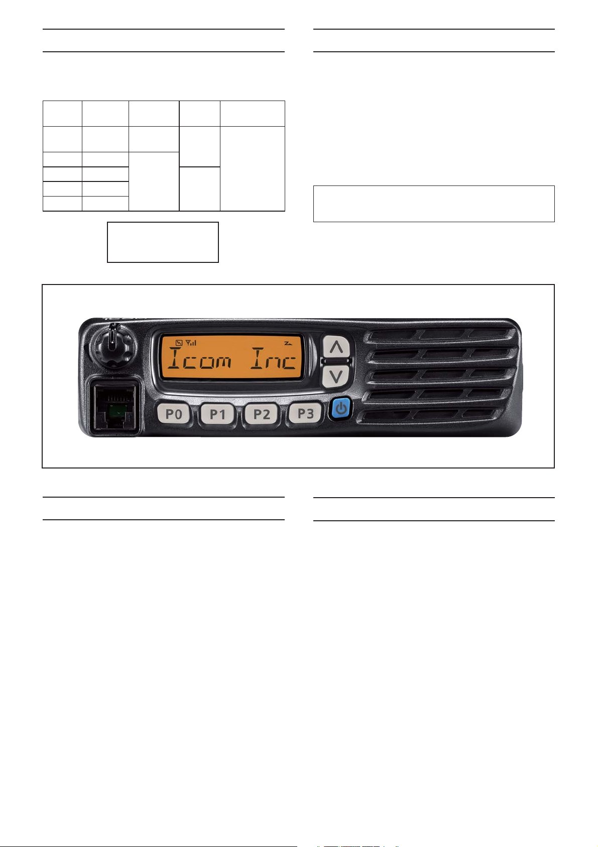
MODEL VERSION
F6022 [EUR-01]
F6023 [EXP-01]
F6021 [USA-01]
F6028H [CHN-01]
UNIT ABBREVIATIONS:
F=FRONT UNIT
M=MAIN UNIT
CHANNEL
SPACINGTXPOWER
12.5/20.0/
25.0 kHz
12.5/25.0
kHz
25 W
45WF6023H [EXP-01]
FREQUENCY
RANGE
400–470 MHz
NEVER connect the transceiver to an AC outlet or to a DC
power supply that uses more than specified. This will ruin
the transceiver.
DO NOT expose the transceiver to rain, snow or any liquids.
DO NOT reverse the polarities of the power supply when
connecting the transceiver.
DO NOT apply an RF signal of more than 20 dm (100 mW) to
the antenna connector. This could damage the transceiver’s
front-end.
To upgrade quality, any electrical or mechanical parts
and internal circuits are subject to change without notice
or obligation.
ORDERING PARTS
Be sure to include the following four points when ordering
replacement parts:
1. 10-digit Icom parts numbers
2. Component name
3. Equipment model name and unit name
4. Quantity required
<ORDER EXAMPLE>
1110003491 S.IC TA31136FNG IC-F6022 MAIN UNIT 5 pieces
8820001210 Screw 2438 screw IC-F6023 Top cover 10 pieces
Addresses are provided on the inside back cover for your
convenience.
REPAIR NOTES
1. Make sure that the problem is internal before
disassembling the transceiver.
2. DO NOT open the transceiver until the transceiver is
disconnected from its power source.
3. DO NOT force any of the variable components. Turn
them slowly and smoothly.
4. DO NOT short any circuits or electronic parts. An
insulated tuning tool MUST be used for all adjustments.
5. DO NOT keep power ON for a long time when the
transceiver is defective.
6. DO NOT transmit power into a Standard Signal
Generator or a Sweep Generator.
7. ALWAYS connect a 50 dB to 60 dB attenuator between
the transceiver and a Deviation Meter or Spectrum
Analyzer when using such test equipment.
8. READ the instructions of test equipment throughly
before connecting a test equipment to the transceiver.
Icom, Icom Inc. and ICOM logo are registered trademarks of Icom Incorporated (Japan) in the United States, the United
Kingdom, Germany, France, Spain, Russia and/or other countries.

TABLE OF CONTENTS
SECTION 1 SPECIFICATIONS
SECTION 2 INSIDE VIEWS
SECTION 3 DISASSEMBLY INSTRUCTION
SECTION 4 OPTIONAL UNIT INSTALLATION
SECTION 5 CIRCUIT DESCRIPITON
5-1 RECEIVER CIRCUITS. . . . . . . . . . . . . . . . . . . . . . . . . . . . . . . . . . . . . . . . . . . . . . . . . . . . . . . . 5-1
5-2 TRANSMITTER CIRCUITS . . . . . . . . . . . . . . . . . . . . . . . . . . . . . . . . . . . . . . . . . . . . . . . . . . . . 5-3
5-3 FREQUENCY SYNTHESIZER CIRCUITS . . . . . . . . . . . . . . . . . . . . . . . . . . . . . . . . . . . . . . . . 5-4
5-4 VOLTAGE BLOCK DIAGRAM . . . . . . . . . . . . . . . . . . . . . . . . . . . . . . . . . . . . . . . . . . . . . . . . . . 5-4
5-5 PORT ALLOCATIONS . . . . . . . . . . . . . . . . . . . . . . . . . . . . . . . . . . . . . . . . . . . . . . . . . . . . . . . . 5-5
SECTION 6 ADJUSTMENT PROCEDURE
6-1 PREPARATION . . . . . . . . . . . . . . . . . . . . . . . . . . . . . . . . . . . . . . . . . . . . . . . . . . . . . . . . . . . . . 6-1
6-2 FREQUENCY ADJUSTMENT . . . . . . . . . . . . . . . . . . . . . . . . . . . . . . . . . . . . . . . . . . . . . . . . . . 6-4
6-3 TRANSMIT ADJUSTMENT . . . . . . . . . . . . . . . . . . . . . . . . . . . . . . . . . . . . . . . . . . . . . . . . . . . . 6-5
6-4 RECEIVE ADJUSTMENT . . . . . . . . . . . . . . . . . . . . . . . . . . . . . . . . . . . . . . . . . . . . . . . . . . . . . 6-6
SECTION 7 PARTS LIST
SECTION 8 MECHANICAL PARTS
SECTION 9 BOARD LAYOUTS
SECTION 10 GENERAL WIRING
SECTION 11 BLOCK DIAGRAM
SECTION 12 VOLTAGE DIAGRAM
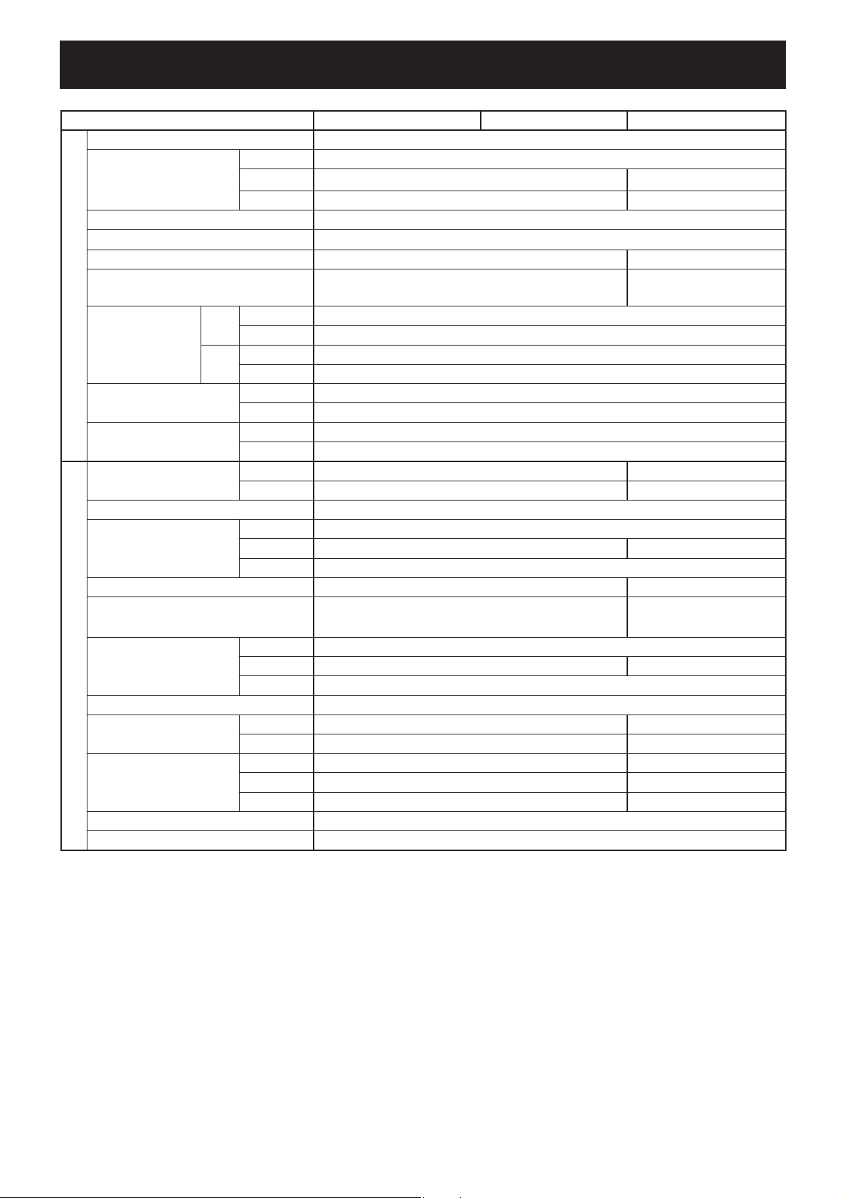
SECTION 1. SPECIFICATIONS
[USA], [CHN] [EXP] [EUR]
• Frequency coverage 400–470 MHz
• Type of emission Wide 16K0F3E (25.0 kHz)
Middle – 14K0F3E (20.0 kHz)
Narrow 11K0F3E (12.5 kHz) 8K50F3E (12.5 kHz)
• Number of programable channels 128 channels (8 zones)
• Antenna impedance
• Operating temperature range −30˚ to +60˚; −22˚F to +140˚F –25˚C to +55˚C
• Power supply requirement
(negative ground)
• Current drain
GENERAL
(approx.)
• Dimensions
• Weight
• Transmit output power [25 W ver.] 25 W (High), 10 W (Low2), 2.5 W (Low1) 25 W
• Modulation Variable reactance frequency modulation
• Max. permissible deviation Wide ±5.0 kHz
• Frequency error ±2.5 ppm ±1.5 kHz
• Spurious emission
• Adjacent channel power Wide More than 70 dB
TRANSMITTER
• Audio harmonic distortion 3% typ. (with 1 kHz AF 40% deviation)
• FM hum and noise
(without CCITT filter)
• Residual modulation
(with CCITT filter)
• Limiting charact of modulation 70–100% of max. deviation
• Microphone impedance 600
Measurements made in accordance with TIA-603 or EN 300 086.
All stated specifications are subject to change without notice or obligation.
Stand-by 250 mA
RX
Max.audio 700 mA
TX
at 25 W 5.0 A
at 45 W 11.0 A
[25 W ver.]
[45 W ver.]
[25 W ver.] 0.8 kg (1
[45 W ver.] 1.1 kg (2
[45 W ver.] 45 W (High), 25 W (Low2), 4.5 W (Low1) –
Middle – ±4.0 kHz
Narrow ±2.5 kHz
Middle – More than 70 dB
Narrow More than 60 dB
Wide More than 40 dB (46 dB typ.) –
Narrow More than 34 dB (40 dB typ.) –
Wide –
Middle –
Narrow –
150 (W) × 40 (H) × 117.5 (D) mm; (5 29/32 (W) × 1 9/16 (H) × 4 5/8 (D) in)
150 (W) × 40 (H) × 167.5 (D) mm; (5 29/32 (W) × 1 9/16 (H) × 6 19/32 (D) in)
13.6 V DC (nominal) 13.2 V DC (nominal)
70 dB typ.
50 Ω (nominal)
3
4
Ib)
/
7
16
Ib)
/
Ω
0.25 μW (≤1 GHz),
1.0 μW (>1 GHz)
More than 45 dB (55 dB typ.)
More than 43 dB (53 dB typ.)
More than 40 dB (50 dB typ.)
1 - 1
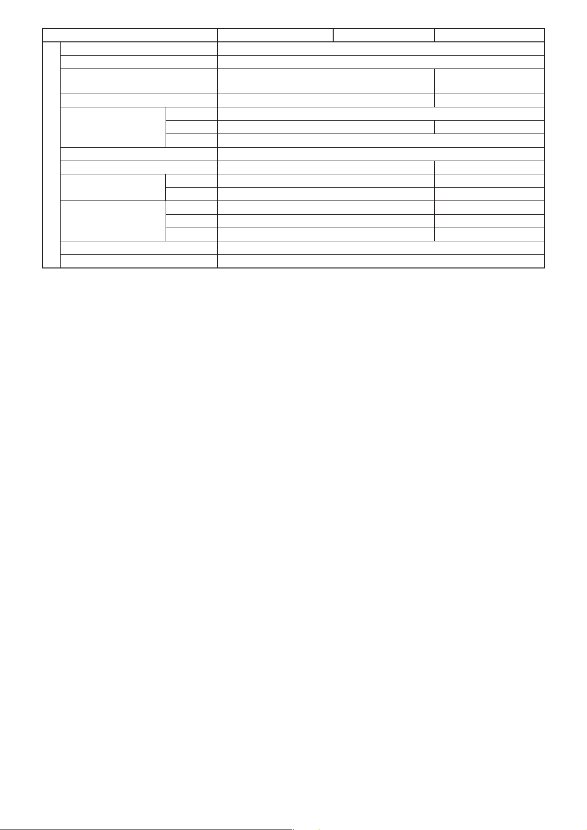
[USA], [CHN] [EXP] [EUR]
• Receive system Double-conversion superheterodyne
• Intermediate frequencies 1st IF; 46.35 MHz, 2nd IF; 450 kHz
• Sensitivity
0.25 μV typ. at 12 dB SINAD
−4 dBμV (EMF) typ.
at 20 dB SINAD
• Squelch sensitivity (at threshold) 0.25 μV typ. –4 dBμV (EMF) typ.
• Adjacent channel
selectivity
Wide More than 70 dB (75 dB typ.)
Middle − More than 70 dB (75 dB typ.)
Narrow More than 60 dB (65 dB typ.)
• Spurious response More than 70 dB
• Intermodulation More than 70 dB (75 dB typ.) More than 65 dB (67 dB typ.)
RECEIVER
• Hum and noise
(without CCITT filter)
• Hum and noise
(with CCITT filter)
Wide More than 40 dB (45 dB typ.) –
Narrow More than 34 dB (40 dB typ.) –
Wide –
Middle –
Narrow –
More than 45 dB (55 dB typ.)
More than 43 dB (53 dB typ.)
More than 40 dB (50 dB typ.)
• Audio output power 4.0 W typ. at 5% distortion with a 4 Ω load
• Audio output impedance 4
Measurements made in accordance with TIA-603 or EN 300 086.
All stated specifications are subject to change without notice or obligation.
Ω
1 - 2
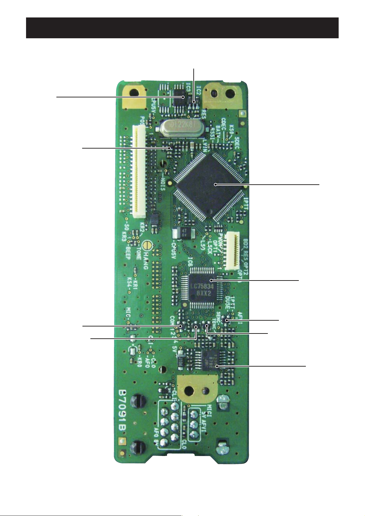
SECTION 2. INSIDE VIEWS
• FRONT UNIT
RESET IC
(IC2)
EEPROM
(IC3)
CLOCK FREQUENCY
SHIFT DIODE
(D6)
BACKLIGHT DRIVER
(Q1)
DIMMER CONTROLLER
(Q2)
CPU
(IC1)
LCD DRIVER
(IC6)
TONE FILTER SWITCH
(Q3)
BACKLIGHT CONTROLLER
(Q5)
2 - 1
TONE LPF
(IC5)
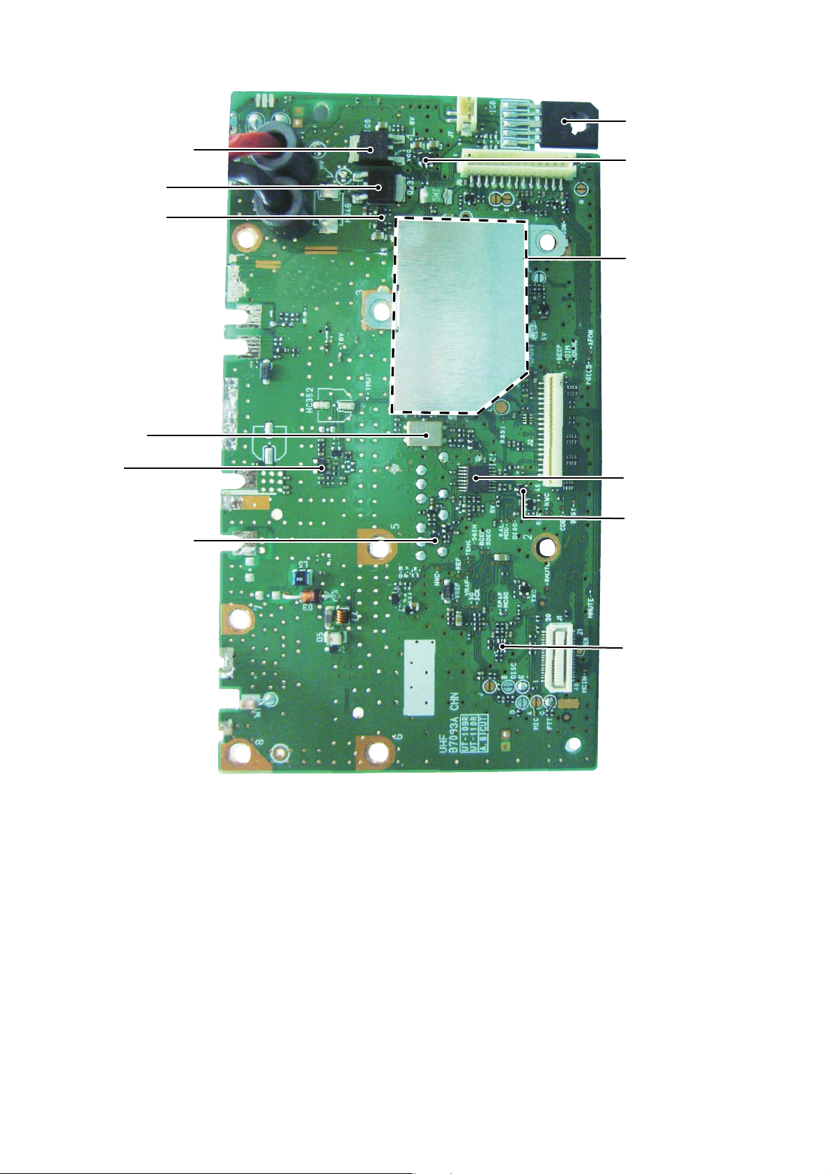
• MAIN-A UNIT
(TOP VIEW)
+8 LINE REGULATOR
POWER SWITCH
(Q23)
POWER SWITCH
(Q24)
(IC9)
AF AMP
(IC8)
CPU5 LINE REGULATOR
(IC10)
PLL CIRCUIT
1ST IF FILTER
(FI1)
APC AMP
(IC2)
2ND IF FILTER SWITCH
(Q40)
IF IC
(IC1)
DISCRIMINATOR SWITCH
(Q5)
LPF
(Q39)
2 - 2
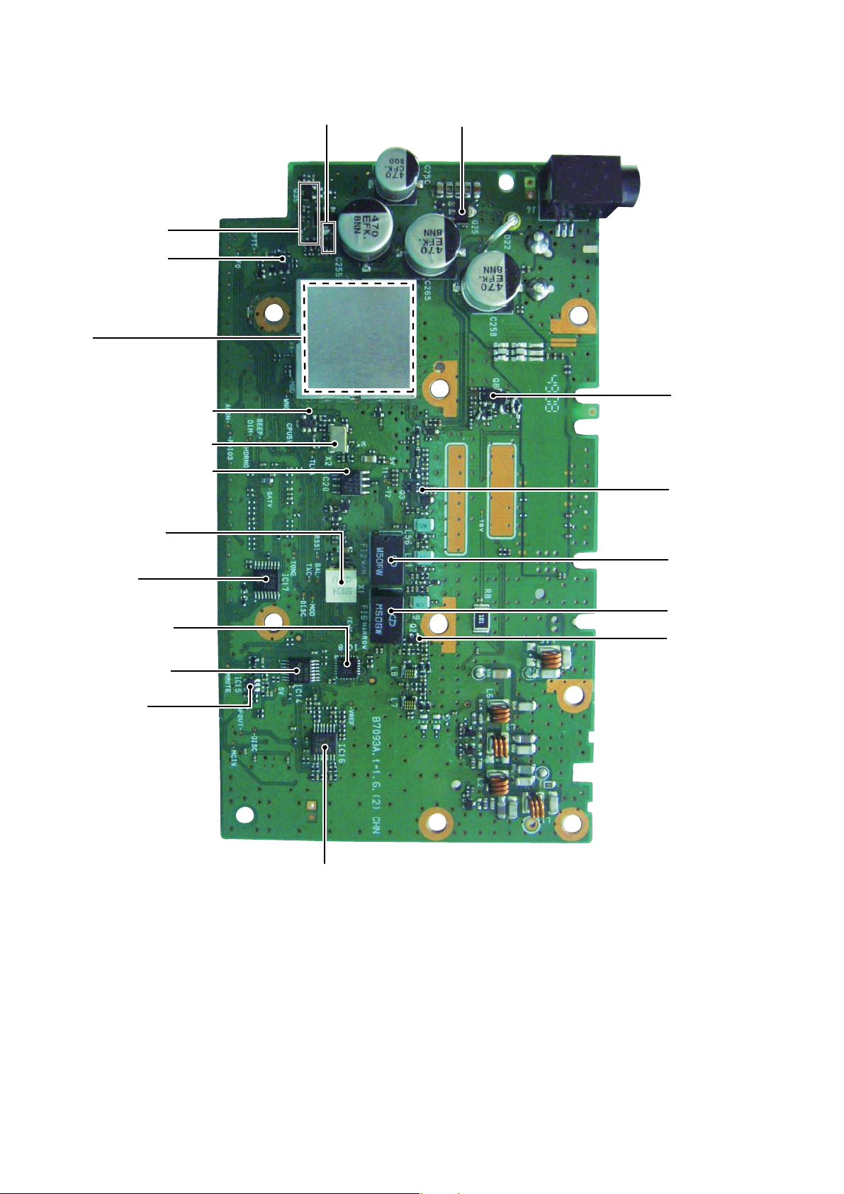
• MAIN-A UNIT
(BOTTOM VIEW)
AF MUTE SWITCH
(Q35, Q36)
Ext. MODULATION
LINE SWITCH
(Q31)
VCO
REFERENCE OSCILLATOR
MODULATION AMP
(IC19)
REFERENCE FREQUENCY
OSCILLATOR (X2)
D/A CONVERTER
(IC20)
+5V LINE REGULATOR
(Q27,Q28)
T8 LINE REGULATOR
(Q25)
DRIVE AMP
(Q9)
1ST MIXER
(Q3)
DISCRIMINATOR
(X1)
EXPANDER
(IC17)
D/A CONVERTER
(IC18)
ANALOG SWITCH
(IC14)
AF PRE-AMP
(IC15)
2ND IF FILTER
(FI2)
2ND IF FILTER
(FI6)
RF AMP
(Q2)
AF/TONE FILTERS
(IC16)
2 - 3
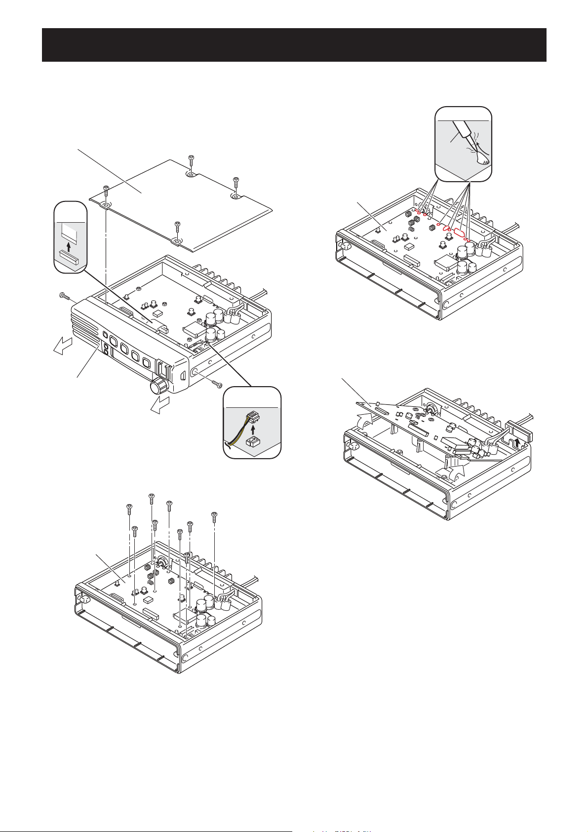
SECTION 3. DISASSEMBLY INSTRUCTION
1) Unscrew 4 screws from the top cover, and remove the top
cover.
2) Disconnect the fl at cable and speaker cable.
3) Unscrew 2 screws from the both sides, and remove the
front panel in the direction of the arrow.
TOP COVER
FLAT
CABLE
5) Unsolder total of 9 points; 3 points at the antenna
connector, 6 points at the PA module.
UNSOLDER
Solder
remover
MAIN UNIT
6) Take off the MAIN UNIT from the CHASSIS.
FRONT PANEL
4) Unscrew 9 screws from the MAIN UNIT.
MAIN UNIT
MAIN UNIT
SPEAKER
CABLE
(Continued to right above)
3 - 1
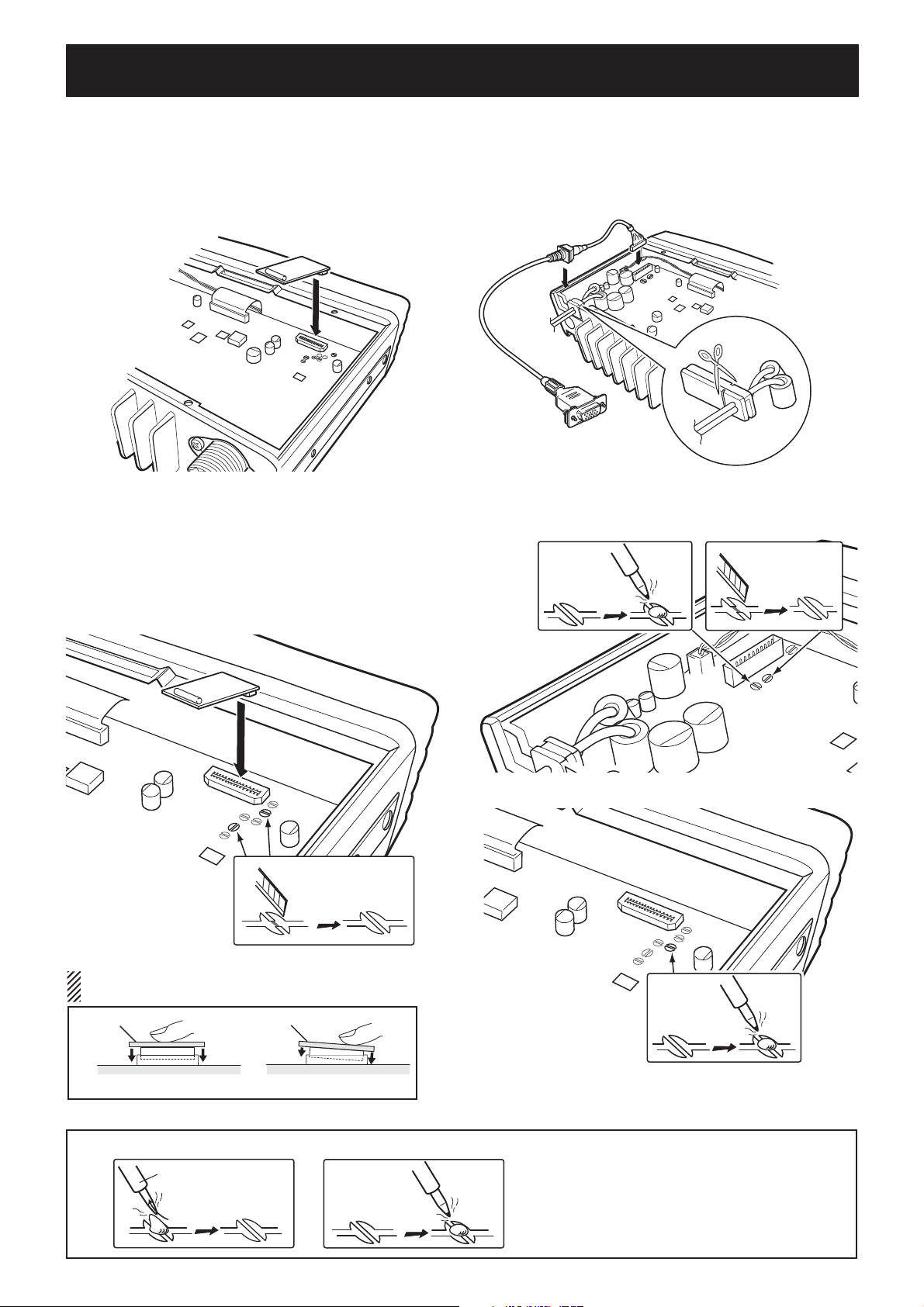
SECTION 4 OPTIONAL PRODUCTS INSTALLATION
Install optional UT-108R as follows;
1) Turn the transceiver power OFF, then disconnect the DC
power cable.
2) Unscrew 4 screws, then remove the bottom cover.
3) Install the unit as shown below.
4) Recover the bottom cover, screws and DC power cable.
Install optional UT-109R or UT-110R as follows;
1) Turn the transceiver power OFF, then disconnect the DC
power cable.
2) Unscrew 4 screws, then remove the bottom cover.
3) Cut the pattern on the PCB at "MIC" and "DISC" as
showon below.
4) Install the unit as shown below.
5) Recover the bottom cover, screws and DC power cable.
Install optional OPC-1939 as follows;
1) Turn the transceiver power OFF, then disconnect the DC
power cable.
2) Unscrew 4 screws, then remove the bottom cover.
3) Install the cable as shown below.
OPC-1939
Cut off the bushing as in the illustration,
when you install the optional OPC-1939.
4) Cut or short the patterns as below. (For AF output)
DISC
MIC
NOTE: When attaching the unit
Be sure that the unit is inserted correctly.
OPTIONAL UNIT
OPTIONAL UNIT
OK
NG
K
I
5) Short the pattern as below. (For modulation input)
D
6) Recover the bottom cover, screws and DC power cable.
NOTE: Be sure to recover the patterns when you remove the optional product. Otherwise no TX modulation or AF output is available.
Solder
remover
4 - 1
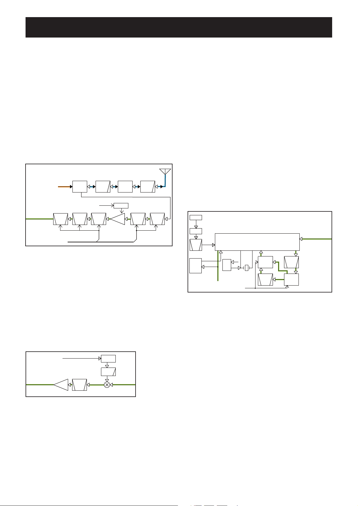
SECTION 5. CIRCUIT DESCRIPTION
t
5-1 RECEIVER CIRCUITS
RF CIRCUITS
RF signals from the antenna are passed through the LPF (as
the harmonic filter for transmitting) and antenna SW, then
applied to the RX BPF circuit.
The applied RX signals are passed through the 2-staged
tuned BPF (D8, 20 and D4, 21) to remove unwanted out-ofband signals, and amplified by the low-noise RF AMP (Q2),
then applied to the 1st mixer (Q3) via three BPFs (D9, 10
and D19).
Each BPF is tuned to the RX frequency by the tuning
voltage “T1” and “T2” from the D/A converter (IC20), to
obtain required IMD characteristic.
• RF CIRCUITS
D3,5,6
From the TX AMP
To 1st IF circuits
D19
BPF
ANT
SW
D10
BPF
D9
BPF
Tuning voltage “T2”
1ST IF CIRCUITS
The RX signals from the BPF are mixed with the 1st LO
signals to be converted into the 46.35 MHz 1st IF signal.
The 1st LO signals are generated by the RX VCO (Q14,
D33, 62, 63), and passed through the LO SW (D15) and
attenuator, then applied to the 1st mixer (Q3)
RSSI
Q1
Q2
D1,11,12
PWR
DET
AGC
RF
AMP
LPFLPF
D4,21
D8,20
BPF
BPF
Tuning voltage “T1”
2ND IF AND DEMODULATOR CIRCUITS
The amplified 1st IF signal is mixed with the 2nd LO signal
at the internal 2nd IF mixer of the IF IC (IC1), to obtain the
450 kHz 2nd IF signal.
The 15.3 MHz signal generated by the reference oscillator
(X2) is passed through the filter AMP (Q34) to extract the
45.9 MHz 3rd harmonic component. The 45.9 MHz signal is
then applied to pin 2 of IF IC (IC1) as the 2nd LO signal.
The converted 2nd IF signal is output from pin 3 of IF IC
(IC1), and filtered by the ceramic filters (FI2 and FI6 for
Narrow mode; FI2 only for Wide mode) to remove unwanted
out-of-band signals, then applied to the internal frequencydemodulator of IF IC (IC1) from pin 5.
The demodulator is a quadrature type which uses X1 as the
phase shifter.
The frequency-demodulated AF signals are output from pin 9
to AF circuits.
• 2ND IF AND DEMODULATORCIRCUITS
X2
REF
15.3MHz
X3
Q34
BPF
D/A
IC18
AK2330
IC1:TA31136FN
45.9MHz
SQIN
DISC
To the AF circuits
IF IC
Q5
NWC
W/N
SW
D57
W/N
X1
SW
FI6
450kHz
CERAMIC
BPF
NWC
FI2
CERAMIC
BPF
D56
W/N
SW
From 1st IF circuits
The converted 1st IF signal is filtered by the crystal filter (FI1)
and amplified by the 1st IF AMP (Q4), then applied to the IF
IC (IC1).
• 1ST IF CIRCUITS
To IF IC
1st LO signals
(182.35 MHz-220.35 MHz)
Q4
IF
AMP
FI1
XTAL
BPF
D14,15
46.35 MHz
1st mixer
To 1st IF circuits
TX/RX
SW
LPF
Q3
From RF circui
5 - 1
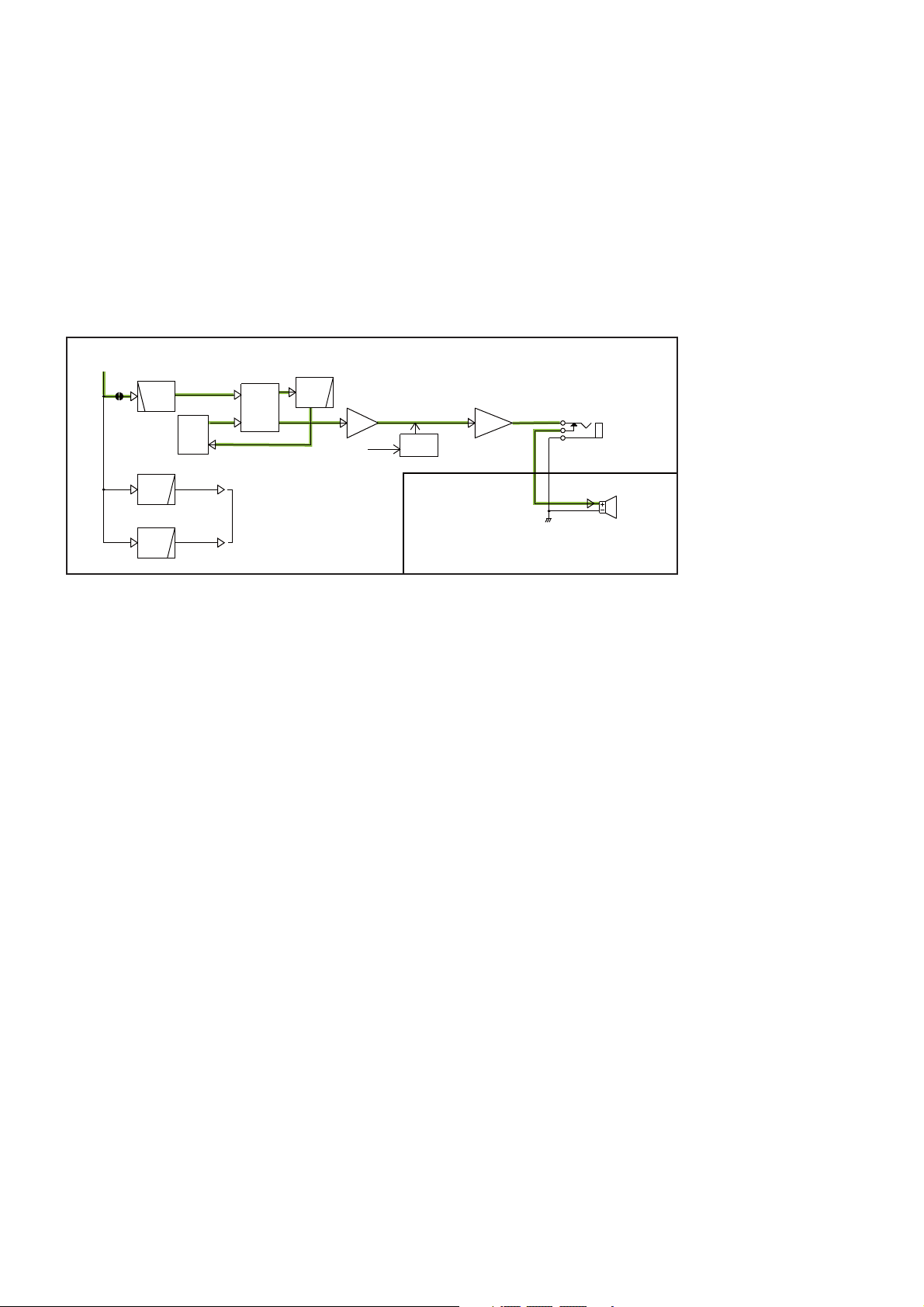
AF CIRCUITS
The demodulated AF signals from the IF IC (IC1) are
amplified and filtered by the HPF (IC16), and passed
through the AF line SW (IC14) and LPF (IC16). The filtered
AF signals are adjusted its level (=loudness) by the D/A
converter (IC18), and applied to the AF AMP (IC15) via the
AF line SW (IC14).
SIGNALING (DECODING)
Demodulated signals from pin 9 of the IF IC (IC1) are
passed through the LPF to extract tone signals contained in
the demodulated signals.
2/5 tone signals are extracted by the LPF (IC16). CTCSS/
DTCS signals are extracted by the LPF (Q39).
The amplified AF signals are applied to the AF power AMP
(IC8) and power-amplified to obtain AF output level.
The power-amplified AF signals are applied to the internal
speaker on the FRONT UNIT or output from the external
speaker jack on the rear panel.
• RX AF CIRCUITS
From the IF IC
DISC
DISC
DISC
IC16
RXAF
HPF
IC16
LPF
(2/5 TONE signals)
Q39
LPF
(TCSS/DTCS signals)
D/A
IC18
AK2330
SDEC
CDEC
IC14
CD4066
ANALOG
VRAF
To CPU (FRONT UNIT: IC1)
IC16
LPF
SW
TMONI
IC15
AF
AMP
AF ON
AF
MUTE
Q35,36,D29
FRONT UNIT
These extracted tone signals are applied to the CPU (FRONT
UNIT: IC1) for decoding.
AF
POWER
AMP
IC8
LA4425A
J4
Ext. speaker jack
Int. speaker
5 - 2
 Loading...