

Page 1

VHF TRANSCEIVER
S-14406XZ-C1
Sep. 2007
Page 2

INTRODUCTION
This service manual describes the latest service information
for the IC-F50V/F51V VHF TRANSCEIVER at the time of
publication.
Model Version Symbol
USA [A]
USA
USA-01 [B] Yes N/A
F50V
Export
Europe
F51V
USA-02 [C] Yes Yes
EXP [D]
EXP-01 [E] Yes N/A
EXP-02 [F] Yes Yes
EUR [G]
EUR-01 [H] Yes N/A
EUR-02 [I] Yes Yes
CHN [J]
China
CHN-01 [K] Yes N/A
CHN-02 [L] Yes Yes
UNIT ABBREVIATIONS:
F=FRONT UNIT
M=MAIN UNIT
V=VR UNIT
CO=CONNECT UNIT
Channel
spacing
(kHz)
15.0/30.0
12.5/25.0
12.5/20.0/25.0
12.5/25.0
Vibration
Voice
storage
N/A N/A
N/A N/A
N/A N/A
N/A N/A
To upgrade quality, any electrical or mechanical parts and
internal circuits are subject to change without notice or
obligation.
CAUTION
NEVER connect the transceiver to an AC outlet or to a DC
power supply that uses more than specified. This will ruin
the transceiver.
DO NOT reverse the polarities of the power supply when
connecting the transceiver.
DO NOT apply an RF signal of more than 20 dBm (100 mW) to
the antenna connector. This could damage the transceiver’s
front-end.
ORDERING PARTS
Be sure to include the following four points when ordering
replacement parts:
1. 10-digit Icom parts numbers
2. Component name
3. Equipment model name and unit name
4. Quantity required
<ORDER EXAMPLE>
1110003491 S.IC TA31136FNG IC-F50V MAIN UNIT 5 pieces
8820001210 Screw 2438 screw IC-F51V Top cover 10 pieces
Addresses are provided on the inside back cover for your
convenience.
REPAIR NOTES
1. Make sure the problem is internal before disassembling
the transceiver.
2. DO NOT open the transceiver until the transceiver is
disconnected from its power source.
3. DO NOT force any of the variable components. Turn
them slowly and smoothly.
4. DO NOT short any circuits or electronic parts. An
insulated tuning tool MUST be used for all adjustments.
5. DO NOT keep power ON for a long time when the
transceiver is defective.
6. DO NOT transmit power into a Standard Signal
Generator or a Sweep Generator.
7. ALWAYS connect a 50 dB to 60 dB attenuator between
the transceiver and a Deviation Meter or Spectrum
Analyzer when using such test equipment.
8. READ the instructions of test equipment throughly
before connecting a test equipment to the transceiver.
Icom, Icom Inc. and
logo are registered trademarks of Icom Incorporated (Japan) in the United States, the United
Kingdom, Germany, France, Spain, Russia and/or other countries.
Page 3

CONTENTS
SECTION 1 SPECIFICATIONS
SECTION 2 INSIDE VIEWS
SECTION 3 DISASSEMBLY INSTRUCTIONS
SECTION 4 CIRCUIT DESCRIPITON
4-1 RECEIVER CIRCUITS. . . . . . . . . . . . . . . . . . . . . . . . . . . . . . . . . . . . . . . . . . . . . . . . . . . . . . . . 4-1
4-2 TRANSMITTER CIRCUITS . . . . . . . . . . . . . . . . . . . . . . . . . . . . . . . . . . . . . . . . . . . . . . . . . . . . 4-3
4-3 FREQUENCY SYNTHESIZER CIRCUITS . . . . . . . . . . . . . . . . . . . . . . . . . . . . . . . . . . . . . . . . 4-6
4-4 OTHER CIRCUITS . . . . . . . . . . . . . . . . . . . . . . . . . . . . . . . . . . . . . . . . . . . . . . . . . . . . . . . . . . 4-7
4-5 VOLTAGE BLOCK DIAGRAM . . . . . . . . . . . . . . . . . . . . . . . . . . . . . . . . . . . . . . . . . . . . . . . . . . 4-7
4-6 CPU (F: IC401) PORT ALLOCATIONS . . . . . . . . . . . . . . . . . . . . . . . . . . . . . . . . . . . . . . . . . . . 4-8
SECTION 5 ADJUSTMENT PROCEDURES
5-1 PREPARATION . . . . . . . . . . . . . . . . . . . . . . . . . . . . . . . . . . . . . . . . . . . . . . . . . . . . . . . . . . . . . 5-1
5-2 FREQUENCY ADJUSTMENT . . . . . . . . . . . . . . . . . . . . . . . . . . . . . . . . . . . . . . . . . . . . . . . . . . 5-4
5-3 TRANSMIT ADJUSTMENT . . . . . . . . . . . . . . . . . . . . . . . . . . . . . . . . . . . . . . . . . . . . . . . . . . . . 5-6
5-4 RECEIVE ADJUSTMENT . . . . . . . . . . . . . . . . . . . . . . . . . . . . . . . . . . . . . . . . . . . . . . . . . . . . . 5-10
SECTION 6 PARTS LIST
SECTION 7 MECHANICAL PARTS
SECTION 8 BOARD LAYOUTS
SECTION 9 BLOCK DIAGRAM
SECTION 10 VOLTAGE DIAGRAM
FRONT UNIT (Incl. CONNECT and VR UNITS) . . . . . . . . . . . . . . . . . . . . . . . . . . . . . . . . . . . . 10-1
MAIN UNIT (Left side) . . . . . . . . . . . . . . . . . . . . . . . . . . . . . . . . . . . . . . . . . . . . . . . . . . . . . . . . 10-2
MAIN UNIT (Right side) . . . . . . . . . . . . . . . . . . . . . . . . . . . . . . . . . . . . . . . . . . . . . . . . . . . . . . . 10-3
Page 4

SECTION 1 SPECIFICATIONS
M GENERAL
• Frequency coverage : TX/RX 136–174 MHz
• Number of conventional channels : 128 ch / 8 banks
• Type of emission : Wide 16K0F3E (25.0 kHz)
• Antenna impedance : 50 Ω (Nominal)
• Operating temperature range : –30˚C to +60˚C; –22˚F to +140˚F [USA], [EXP], [CHN]
• Power supply requirement (nominal) : Specified Icom's battery packs only (7.2 V DC; negative ground)
• Current drain (Approx.) : Receiving 85 mA (stand-by)
• Dimensions (Projections not included) : 56.0 (W)×97.0 (H)×36.4 (D) mm; 2
• Weight (Incl. BP-227) : Approx. 280 g; 9
M TRANSMITTER
• Output power : 5 W (High)/2 W (Low2)/1 W (Low1)
• Modulation : Variable reactance frequency modulation
• Maximum frequency deviation : ±5.0 kHz (Wide)
• Frequency stability : ±2.5 ppm
• Spurious emissions : 70 dB typ. [USA], [EXP], [CHN]
• Adjacent channel power : 70 dB min. (Wide, Middle)
• Audio harmonic distortion : 3% (at AF 1 kHz 40% deviation)
• FM Hum and noise (without CCITT filter)
[USA], [EXP], [CHN] only
• Residual modulation (with CCITT filter)
[EUR] only
• Limitting charact of modulator : 60–100% of max. deviation
• Microphone impedance : 2.2 k
Middle 14K0F3E (20.0 kHz) [EUR] only
Narrow 11K0F3E (12.5 kHz)
–25˚C to +55˚C [EUR]
500 mA (max. audio with internal speaker)
350 mA (max. audio with external speaker)
Transmitting 1.8 A (at 5.0 W)
0.7 A (at 1.0 W)
7
/8 oz.
±4.0 kHz (Middle) [EUR] only
±2.5 kHz (Narrow)
0.25 μW (≤1 GHz), 1.0 μW (>1 GHz) [EUR]
60 dB min. (Narrow)
: 40 dB min., 46 dB typ. (Wide)
34 dB min., 40 dB typ. (Narrow)
: 50 dB min., 55 dB typ. (Wide)
43 dB min., 53 dB typ. (Middle)
40 dB min., 50 dB typ. (Narrow)
Ω
7
/32 (W)×3 13⁄16 (H)×1 7⁄16 (D) in.
M RECEIVER
• Receive system : Double-conversion superheterodyne system
• Intermediate frequencies : 1st IF: 46.35 MHz, 2nd IF: 450 kHz
• Sensitivity : 0.25 μV typ. at 12 dB SINAD [USA], [EXP], [CHN]
–4 dBµ V (EMF) typ. at 20 dB SINAD [EUR]
• Squelch sensitivity (at threshold) : 0.25 μV typ. [USA], [EXP], [CHN]
–4 dBµ V (EMF) typ. [EUR]
• Adjacent channel selectivity : 70 dB min., 75 dB typ. (Wide, Middle)
• Spurious response : 70 dB
• Intermodulation rejection ratio : 70 dB min., 74 dB typ. [USA], [EXP], [CHN]
• Hum and noise (without CCITT filter)
[USA], [EXP], [CHN] only
• Hum and noise (with CCITT filter)
[EUR] only
• Audio output power
(at 5% distortion with an 8 Ω load)
• Audio output impedance : 8
Specifications are measured in accordance with TIA/EIA 603 ([USA], [EXP], [CHN]) or EN 300 086 ([EUR]).
All stated specifications are subject to change without notice or obligation.
60 dB min., 65 dB typ. (Narrow)
65 dB min., 67 dB typ. [EUR]
: 40 dB min., 45 dB typ. (Wide)
34 dB min., 40 dB typ. (Narrow)
: 45 dB min., 55 dB typ. (Wide)
43 dB min., 53 dB typ. (Middle)
40 dB min., 50 dB typ. (Narrow)
: 0.7 W typ. (max. audio with internal speaker)
0.5 W typ. (max. audio with external speaker)
Ω
1 - 1
Page 5
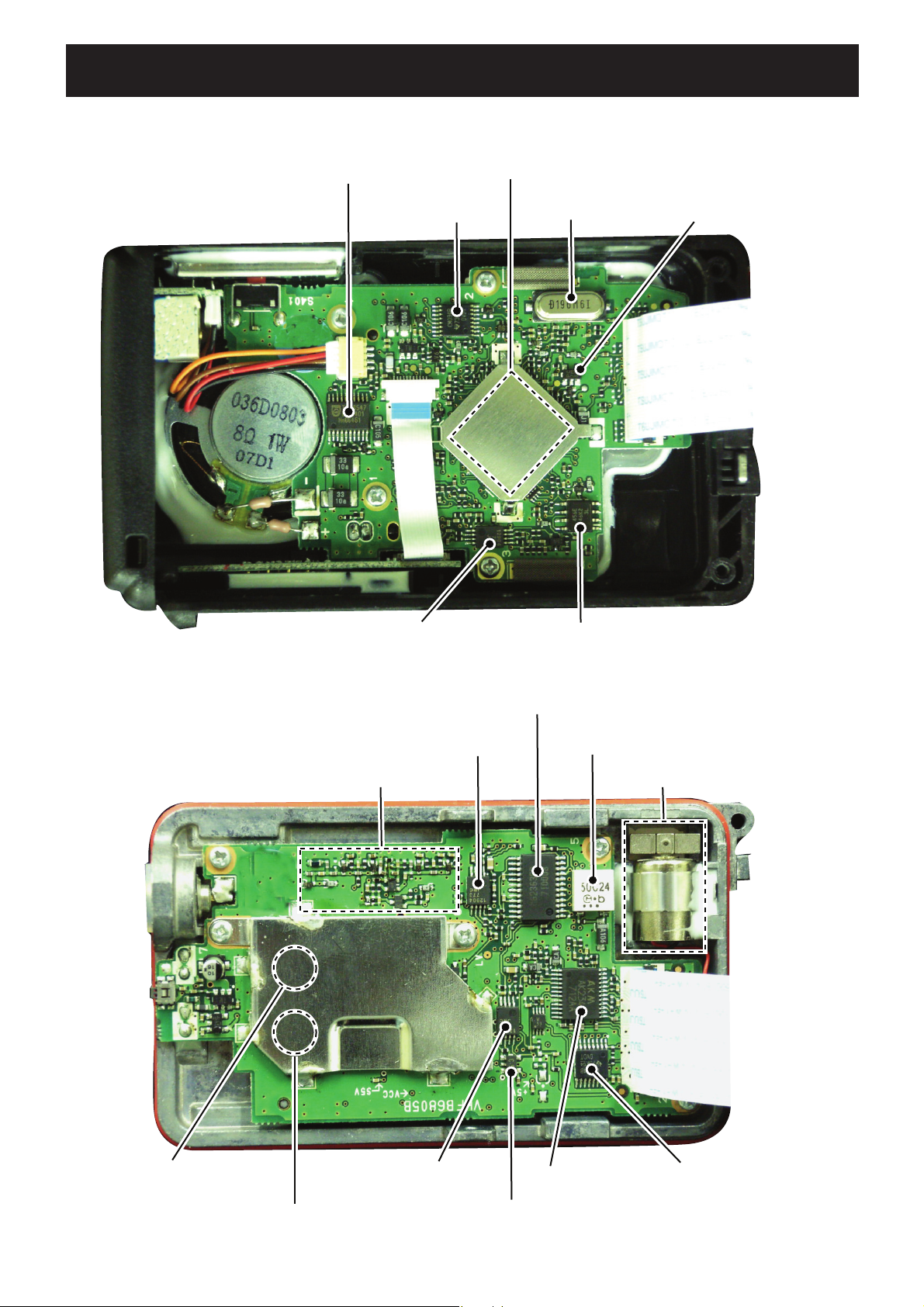
SECTION 2 INSIDE VIEWS
• FRONT UNIT
AF POWER AMP
(IC405: TDA8547TS)
EXPANDER
(IC410: CD4094BPWR)
CPU
(IC401: HD64F2268TFV)
CPU CLOCK
(X401: CR-764)
RESET IC
(IC408: BD5242G)
• MAIN UNIT
MIC AMP
(IC407: NJM12904V)
AF BUFFER, AF MIXER
(IC5: NJM12904V)
RF CIRCUITS
EEPROM
(IC409: HN58X24256FPIE)
DAC
(IC6: M62363FP-650C)
DISCRIMINATOR
(X1: CDBKB450KCAY24)
VIBRATION MOTOR
(MF1: QX10A(R5.5X3))
TX POWER AMP
(Q7: RD07MVS2-T112)
DRIVE AMP
(Q8: RD01MUS1-T113)
AF BUFFER
(IC6: NJM12904V)
LOCK VOLTAGE SWITCH
(IC17: TC4S66F)
2 - 1
BASE BAND IC
(IC10: AK2346)
EXPANDER
(IC12: CD4094BPWR)
Page 6
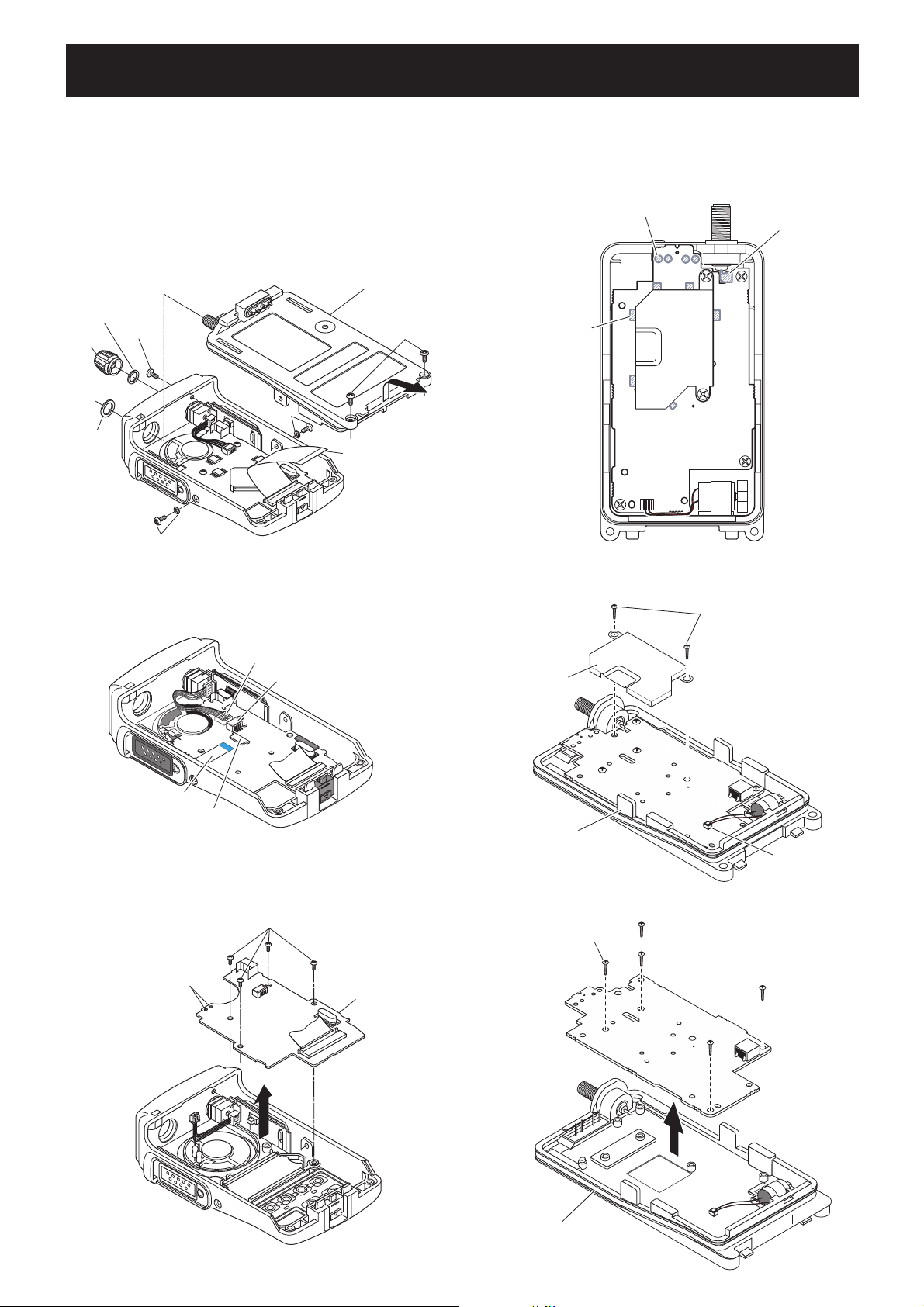
SECTION 3 DISASSEMBLY INSTRUCTION
1. REMOVING THE CHASSIS UNIT
q Unscrew the ANT nut, and remove the VR knob.
w Remove the VR washer, and unscrew the top screw.
e Unscrew side screws and washers.
r Unscrew bottom screws.
t Take off the CHASSIS UNIT in the direction of the
arrow.
y Disconnect the flat cable from the CHASSIS UNIT
(MAIN UNIT).
CHASSIS
VR washer
VR knob
ANT nut
Side screw & Washer
Top screw
Side screw & washer
Bottom screws
Flat cable
2. REMOVING THE FRONT UNIT
q Disconnect the VR cable from J402.
w Disconnect the flat cable from J403.
3. REMOVING THE MAIN UNIT
q Unsolder 6 points from the shield cover.
w Unsolder 4 points from the contact spring.
e Unsolder 1 point from the antenna connector.
Unsolder ×4
(contact spring)
Unsolder ×6
(shield cover)
MAIN UNIT
Unsolder ×1
(antenna connector)
r Unscrew 2 screws, and remove the shield cover.
t
Disconnect the motor connector* from the MAIN UNIT.
Unscrew ×2
VR cable
J402
Flat cable
J403
e Unscrew 4 screws.
r Unsolder 2 points (at the speaker leads).
t Take off the FRONT UNIT in the direction of the
arrow.
Unscrew ×4
Unsolder ×2
(Speaker leads)
FRONT UNIT
Shield cover
CHASSIS
*: Except [A], [D], [G], [J]
MAIN UNIT
Disconnect
(motor connector)
y Unscrew 5 screws, and take off the MAIN UNIT.
Unscrew ×5
MAIN UNIT
*
3 - 1
CHASSIS
Page 7
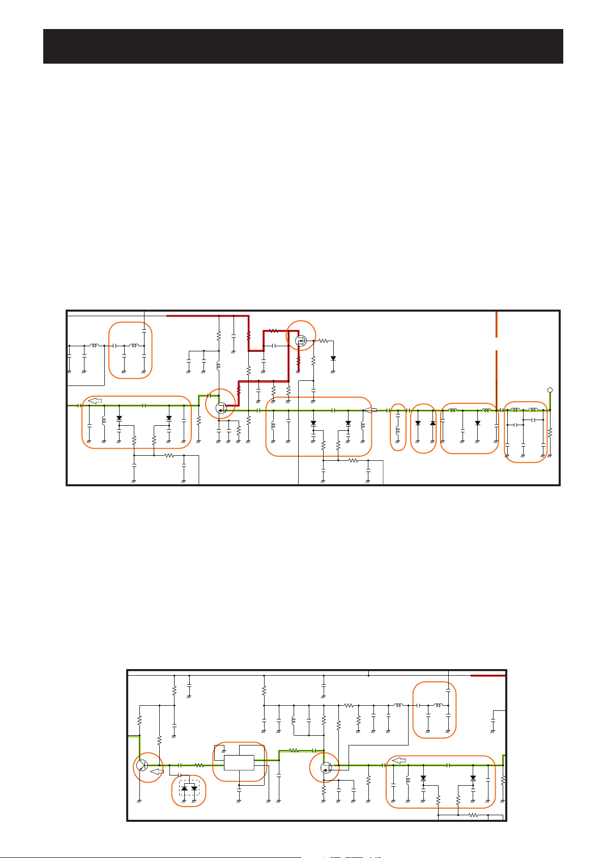
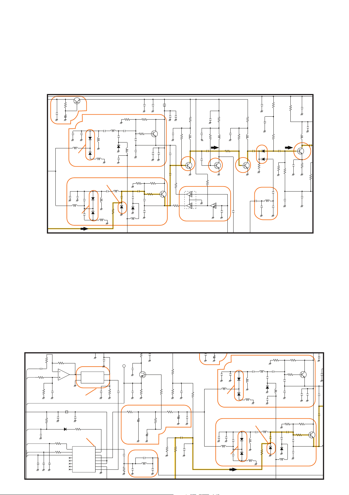
SECTION 4 CIRCUIT DESCRIPTION
4-1 RECEIVER CIRCUITS
RF CIRCUITS
RF circuits consist of RF fi lters, antenna switch (ANT SW),
RF amplifi er (RF AMP), etc., and extracts and amplifi es the
signals of frequency which desired to receive.
The received signals (RX signals) from the antenna are passed
through the LPF, ANT SW (as an LPF in RX), limitter , BEF
(Band Eliminate Filter) and the two-staged tuned BPF. The
fi ltered RX signals are amplifi ed by the RF AMP, and passed
through another two-staged tuned BPF. The fi ltered RX signals
are then applied to the 1st IF circuits.
The ANT SW toggles RX line and TX line. While receiving,
the TX line and the antenna is disconnected to prevent RX
signals entering. The RX line is disconnected from the GND
simultaneously, and an LPF which guides received signals
to the RX circuits is composed.
While transmitting, serial-connected PIN diodes are ON,
thus the TX line is connected to the antenna, and the RX
line is connected to the GND simultaneously to prevent TX
signal entering.
The limitter protects RX line from over-level RF inputs, and
the BEF (=trap) damps unwanted signals to GND.
The tuned-BPF is adjusted so that it responds to receiving
frequency and rejects all others, by the variable capacitor
whose capacitance is varied by added voltage "T1" and "T2."
The RF AMP amplifi es RX signals to a level suited to the 1st
mixer.
• RF CIRCUITS
R5V
L1
2
C322
1stLO
C41
C44
Two-staged
TUNED BPF
LPF
C183
L14
C49
C324
C323
C40
D10
L11
C45
R23
C43
D9
C39
R21
R22
C42
R17
C35
C36
L9
RF
AMP
C37
Q2
C38
C32
R20
C33
R16
T2
C184
R172
R18
C186
C31
R19
C30
R12
R213
C29
R15
L8
1ST IF CIRCUITS
The 1st IF circuits consist of 1st mixer, 1st IF fi lter and 1st IF
amplifi er (IF AMP). And it converts the RX signals into the
1st IF signal, then filters to remove unwanted signals and
amplifi es.
R171
C28
AGC LINE
Q1
DRIVER
R173
RSSI
R174
D23
R175
Two-staged
C23
TUNED BPF
C22
D4
C26
R13
C27
LIMITTER
C19
C25
6P
D8
L7
C20
R11
R14
BEF
C24
T1
D6
C18
L31
C17
D7
To TX AMP
L6
L5
D5
C16
LPF (ANT SW)
C14
C5
The converted 1st IF signal is passed through the 1st IF fi lter
to be removed unwanted signals. The fi ltered 1st IF signal is
applied to the 1st IF AMP via the limitter. The amplifi ed 1st
IF signal is then applied to the 2nd IF circuits.
L2
C4
C3
LPF
To ANT
L1C6
C2
R51
C1
The filtered RX signals are applied to the 1st mixer to be
converted into the 1st IF signal, by being mixed with the 1st
Local Oscillator (LO) signals “1stLO” from the RX VCO via
the LPF.
• 1ST IF CIRCUITS
R5V R5V
56
FL-335
R31
C53
C54
FI1
1
IN
C55
R48
1stIF
Q4
R34
1st IF
AMP
C329
C59
R35
C60
C58
R33
D26
LIMITTER
1st IF
FILETR
4
GND
2
OU T3GND
C56
L13
R32
1st
MIXER
4 - 1
C51
R5V
C57
R27
C322
C321
C52
R30
1
Q3
R29
R26
R28
C50
1stLO
C41
R25
C48
LPF
C183
L1
2
C44
L14
C49
C324
C323
C40
D10
L11
C45
R21
R23
C35
C36
D9
C38
R20
C39
Two-staged
Page 8
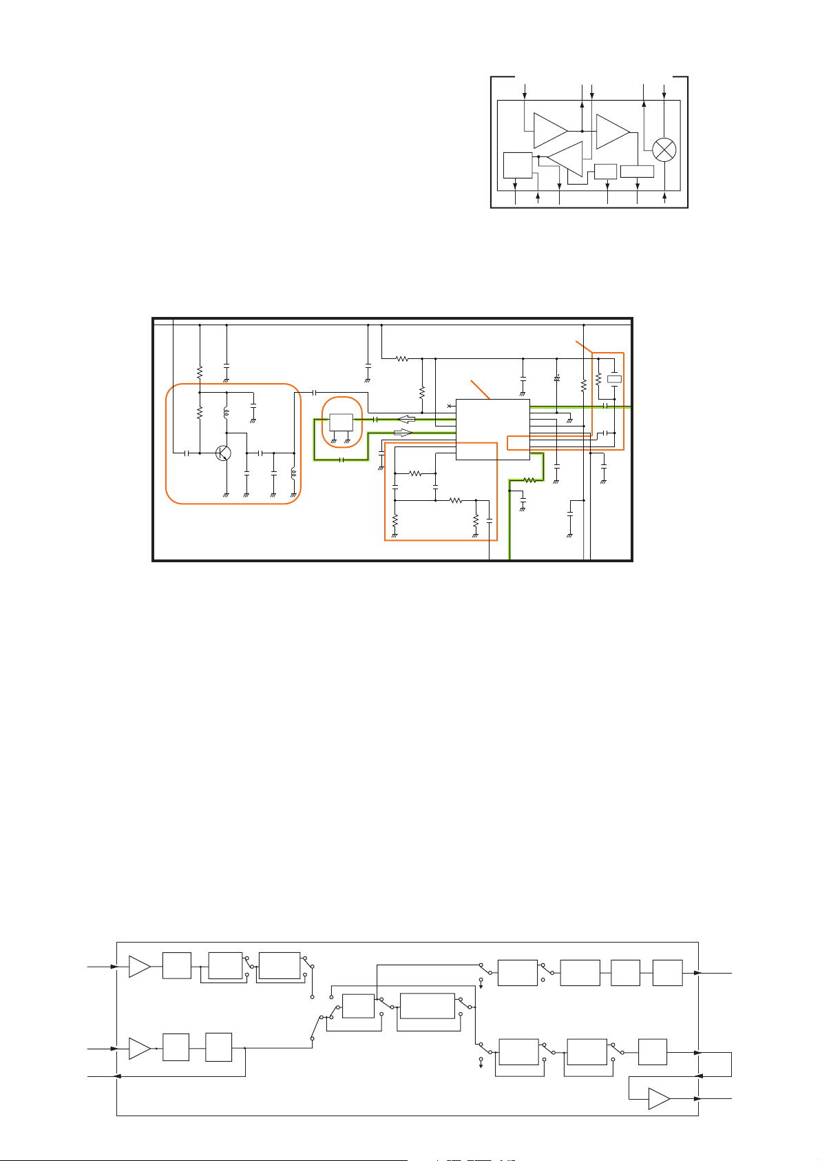
2ND IF AND FM DEMODULATOR CIRCUITS
The 2nd IF circuits consist of 2nd mixer, 2nd IF filter, 2nd
IF amplifier. And it converts the 1st IF signal into the 2nd
IF signal, then filters to remove unwanted signals and
amplifi es. IF IC "TA31136FNG" contains whole of the 2nd IF
circuits and FM demodulator circuit too.
The 1st IF signal is applied to the IF IC, and converted into
the 2nd IF signal, by being mixed with the 2nd LO signal
(from the X2 via the PLL IC (IC4, pins 1, 2) and tripler), at
internal 2nd mixer. The converted 2nd IF signal is filtered by
external 2nd IF filter (ceramic filter), and saturation-amplified
by internal 2nd IF AMP. The amplified 2nd IF signal is
F
M-demodulated by the quadrature detector.
The demodulated AF signals "SQLI" are applied to the RX
AF circuits.
• 2ND IF AND FM DEMODULATOR CIRCUITS
R115
R116
C185
C166
C165
L35
Q19
C162
C163
C164
L33
2nd IF
FILTER
FI2
C169
C167
IO
C168
C71
Ref.Freq.
C161
TRIPLER
(×3)
R46
R39
R44
C69
R40
C70
NOISE
FILTER
IF IC
IC1
1
OSCIN
2
OSCOUT
3
M IXOUT
4
VCC
5
IFIN
6
DEC
7
FILOUT
8
FILIN
TA31136FNG
R45
C68
R42
SQLO
IF IC (TA31136FNG) BLOCK DIAGRAM
FM
Detector
9
8
73
5
Noise
Filter
2nd IF
AMP
1110
Noise
AMP
RSSI
Noise Det.
12
QUADRATURE
DETECTOR
MIXIN
N-REC
N-DET
IFOUT
AFOUT
SQLI
RSSI
QUAD
C67
16
15
GND
14
13
12
11
10
9
R43
C188
C66
C75
1stIF
C63
R36
X1
R38
C61
C62
C65
NOIS
RSSI
2
2nd
Mixer
14
16
RX AF CIRCUITS
The RX AF circuits consist of AF filters, AF amplifier (AF
AMP), AF power amplifier, etc., and amplify, filter the AF
signals FM-demodulated by the FM IF IC.
This transceiver employs the base band IC for audio signal
processing for both transmit and receive. The base band
IC is an audio processor and composed of RF AMPlifier,
compressor, expander, scrambler, etc. in its package.
The demodulated AF signals from the IF IC are applied to
the base band IC (IC10, pin 23). The applied AF signals are
amplified at the amplifier section and level adjusted at the
volume controller section, then suppressed unwanted 3 kHz
and higher audio signals at LPF. The filtered AF signals are
applied (bypassed) the TX/RX HPF, scrambler, de-emphasis
sections in sequence.
• BASE BAND IC BLOCK DIAGRAM
Com-
pressor
TXA1
VR1
(HPF)
3 TXIN
Pre-
emphasis
TX/RX
HPF
The TX/RX HPF filters out 250 Hz and lower audio signals,
and the de-emphasis circuit obtains –6 dB/oct of audio
characteristics. The expander expands the compressed
audio signals and also noise reduction function is provided.
The AF signals are then level adjusted at the volume
controller section and amplified at the amplifier section, then
output from pin 20 (IC10).
The processed AF signals from the base band IC (IC10) are
applied to the FRONT UNIT via J1 (MAIN) and J401
(FRONT).
The AF signals from the MAIN UNIT
"SIGNAL" are passed
through the AF mute SW, LPF and variable register (VR
UNIT) for audio level adjustment, then applied to the AF
power AMP. The amplified AF signals
"AFO" are applied to
the internal speaker, or external speaker via the [SP MIC]
jack (MP701; CHASSIS).
BASE BAND IC (IC10)
SMF
7 MOD
Scrambler/
De-scrambler
Limiter Splatter VR2
23 RXIN
21 SDEC
RXA1
VR3
(HPF)
RX
LPF
4 - 2
De-
emphasis
Expander
VR4
RXA2
18
19
20
SIGNAL
Page 9

SQUELCH CIRCUITS
• NOISE SQUELCH
The noise squelch cuts off the AF output signals when
no RF signals are received. Extracting noise components
(approx. 30 kHz signals) in the demodulated AF signals,
the squelch circuit turns the AF power amplifier and AF
switches ON and OFF.
A portion of FM-demodulated AF signal from the IF IC is
adjusted its level (=squelch threshold level) by DAC (D/A
converter; IC6, pins 1, 2), then passed through the noise
filter (M: IC1, pins 7, 8 and R42, 44–46, C68–70) to extract
the noise components (approx. 30 kHz signals) only. The
noise components are rectified to be
pulse-type signal
by noise detector to produce DC voltage
corresponding to the noise level "NOIS". Then the DC
voltage is applied to the CPU (IC401, pin 41) and compared
with the reference level preset in the CPU.
If the CPU interpretes that the noise level is higher than
preset one, the CPU sets the "AFON" signal to "High" to
turn the AF power AMP controller OFF, and the AF mute
SW is turned OFF simultaneously. Thus closing the squelch
is accomplished.
To RX AF circuits
From IF IC (Pin16)
NOISE SQUELCH DIAGRAM
1 2
DAC
Fc=30 kHz
Noise
AMP
Active filter
converted into the
Rectify
“NOIS”
Noise detector
• TONE SQUELCH
The tone squelch connects the RX AF line and activates
the AF power amplifier to emit the AF signals only when
receiving a signal which contains the tone frequency
matched with preset in the CPU. Detecting signal in the
demodulated AF signals, the tone squelch circuit turns the
AF power amplifier and AF switches ON and OFF.
<CTCSS/DTCS>
A portion of FM-demodulated AF signals from the FM IF
IC are passed through the tone filter (M: Q6, pins 5, 6) to
remove unwanted voice siganls. The filtered tone signals
are applied to the CPU (IC401, pin 44).
<2/5 TONE, DTMF>
A portion of FM-demodulated AF signals are output from
the baseband IC (M: IC10, pin 21), and passed through
the tone filter (M: R136, C220) to remove unwanted voice
siganls. The filtered tone signals are applied to the CPU
(IC401, pin 43).
The CPU compars the tone frequency/code preset in the
CPU, and if the applied tone frequency/code is matched to
preset one, the CPU controls the AF power AMP and AF
mute SW as same as "NOISE SQUELCH."
4-2 TRANSMITTER CIRCUITS
TX AF CIRCUITS
The TX AF circuits consist of microphone amplifier (MIC
AMP) and AF fi lters. The AF fi lter cuts off the signals except
voice signals (300 Hz or lower and 3 kHz or higher).
The audio signals from the internal microphone (MIC
signals) are passed through MIC mute SW and amplifi ed by
two MIC AMPs (#1 and #2).
• TX AF CIRCUITS
AFO
R401
C404
AUDIO
VR UNIT
SP401
W601
4
3
2
1
LEVEL
ADJUST
J402
56
1
2
3
4
W401
Q413
R445
W402
BPMAX
R446
PWON
C502
C503
C426
C496
C435
MC401
R434
R517
R518
C437
R519
R520
R402
R521
R522
R541
C423
C401
R430
C425
R432
13
14
12
IC403
LPF
C513
R537
The MIC signals from the external microphone "EXMIC” are
applied to the FRONT UNIT via [SP MIC] jack, and amplifi ed
by MIC AMP (#2).
The amplified MIC signals "MIC” are applied to the MAIN
UNIT via J401(FRONT UNIT) and J1 (MAIN UNIT).
The MIC signals from the FRONT UNIT are applied to the
baseband IC (IC10, pin 3) and processed.
5
8
7
6
IC406
MUTE SW
1
2
3
4
C497
R433
C482
C512
Q415
R538
AF POWER AMP
IC405
20
19
18
17
16
15
14
13
12
11
VCC1
NC
OUT1IN1IN1+
IN2+
IN2OUT2NC
VCC2
R523
R539
GND1
OUT1 +
MODE
SVRR
SELECT
OUT2 +
GND2
NC
NC
NC
MIC/AF
MIC AMP
R513
R408
C481
R535
1
2
3
4
5
6
7
8
9
10
C510
#1
2
3
C498
R511
R429
R524
IC407
Q406
1
R426
R428
R525
EXMIC
R406
R405
R512
Q401, Q402
MIC AMP
C407
R407
6
5
C406
C405
C421
AF POWER AMP
CONTROLLER
#2
IC407
AFON
7
DUSE
BEEP
MIC
SIGNAL
AFON
VCC
SPON
4 - 3
Page 10
VCC
The applied MIC signals are amplified at the amplifier
(TXA1), and level adjusted at the volume controller (VR1).
The level adjusted MIC signals are applied (bypassed) the
compressor section, pre-emphasis section, TX/RX HPF,
de-scrambler, limiter, splatter, in sequence, then applied to
another volume controller.
The compressor compresses the MIC signals to provide
high S/N ratio for receive side, and the pre-emphasis obtains
+6 dB/oct audio characteristics. The TX/RX HPF fi lters out
250 Hz and lower audio signals, the limiter limits its level and
the splatter fi lters out 3 kHz and higher audio signals. The
filtered MIC signals are level adjusted at another volume
controller (VR2), and then output from pin 7 via smoothing
fi lter (SMF).
The output MIC signals are passed through the FM/PM
SW (IC11, pins 6, 1) and LPF (IC5, pins 2, 1) then applied
to the DAC (D/A Converter; IC6, pin 4) and level-adjusted
(deviation adjustment). The level-adjusted MIC siganls are
output from pin 3, then applied to the modulation circuit as
the modulation signals
"MOD” via buffer (IC5, pins 6, 7).
<CTCSS/DTCS>
CTCSS/DTCS signals ("CEN0"–"CEN2") are generated by
the CPU (F: IC401, pins 79–81) and converted its wave
form by R461–R463 (F), then passed through the LPF (F:
IC403, pins 3, 1). The fi ltered CTCSS/DTCS signals are
then level-adjusted by DAC (M: IC6, pins 9, 10) and applied
to the AF mixer (M: IC5, pin 2) to be mixed with MIC signals,
then applied to the TX VCO as the modulation signals. The
CTCSS/DTCS signals are also applied to the reference
signal oscillator (M; X2) too, via the buffer (M: IC16, pins 2, 1).
<2/5 TONE, DTMF>
2/5 tone and DTMF signals are ("SEN0"–"SEN3") are
generated by the CPU (F: IC401, pins 72–75) and converted
its wave form by R471–R474 (F), then passed through
the two-staged LPF (F: IC403, pins 5, 7 and pins 10, 8).
The filtered 2/5 tone and DTMF signals are applied to the
AF mixer (M: IC5, pin 2) to be mixed with MIC signals.
The mixed signals are then applied to the TX VCO as the
modulation signals). The CTCSS/DTCS signals are also
applied to the reference signal oscillator (M: X2, pin 1) too,
via the buffer (M: IC16, pins 2, 1).
MODULATION CIRCUIT
The modulation circuit FM-modulates the VCO oscillating
signal with the modulation signals from the TX AF circuits.
• VOICE SIGNAL
The buffer-amplified AF signals are applied to the variable
capacitor (VD) to change its reactance for FM modulation.
• TONE SIGNALS
Tone signals are generated in the CPU and applied to the
both of the VCO and reference frequency oscillator to be
modulated.
• MODULATION CIRCUIT AND TX/RX VCOs
RIPPLE
C148
C190
C191
L28
Freq.
adjust
TX VCO
C195
L27
Freq.
adjust
Q17
FILTER
RX VCO
D1 9
C194
C192
C193
C127
D2 0
L37
L39
Modulation
C124
D17
L24
D1 6
L38
L26
C139
R79
R85
C126
C134
D22
L42
C203
L25
C129
D18
R86
L43
LVA
Q14
R81
C114
C115
C119
R84
R83
C123
R82
C133
C121
D21
C122
R98
C137
LV
MOD
The modulated VCO output is buffer-amplifi ed by two buffers
(Q12, Q10), and applied to the pre-driver via TX/RX SW.
T5V
C110
Q13
from VCO
C120
EP1
C116
C104
C118
R88
C117
C113
Q12
BUFFER
R87
Q15
5
R78
R77
VCO
SW
C109
R76
R75
C105
C102
C103
1
2
34
L41
R72
Q11
R80
Q16
C111
R5V
C107
R71
BUFFERBUFFER
C205
To PLL
R70
L21
C100
Q10
1stLO
C108
C99
TX/RX
SW
D14
D15
R69
LPF
L14
C49
C323
0.01
0.001
TX
R68
R67
C93
C183
C324
R65
C95
4 - 4
Page 11
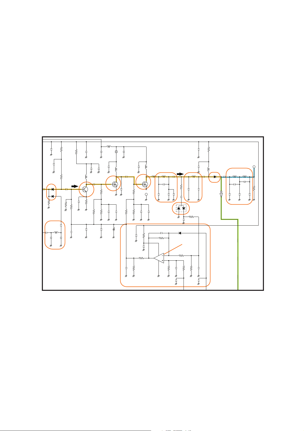
TRANSMIT AMPLIFIERS
0
The transmit amplifiers consist several RF amplifiers (predriver, driver, power), and amplify the TX VCO output to the
transmit output level.
The TX VCO output is applied to the pre-drive amplifi er
via
the TX/RX switch. The amplified TX signal is amplified by
drive amplifier, then power-amplified by the power amplifier
to obtain 5 W (max.) of TX output power.
The power-amplified TX signal is passed through the LPFs
(as a harmonic filter), ANT SW (TX), and another LPF, then
applied to the antenna.
• TRANSMIT AMPLIFIERS AND APC CIRCUIT
L20
R68
C108
TX/RX
SW
0
R69
LPF
C49
C323
0.01
C99
0.001
R67
D14
C93
TX
D15
R65
C183
L14
C95
C324
R61
Pre-
DRIVE
R63
C106
C96
C97
DRIVE
L19
AMP
C92
Q9
C90
R62
R59
C91
C94
C292
R58
EP2
C81
C85
L18
Q8
C87
R57
C89
C88
C98
C82
C86
Q7
R53
R54
R55
C77
C76
R9
R10
C73
APC CIRCUIT
APC CIRCUIT
The APC (Automatic Power Control) circuit stabilizes
transmit output power to prevent transmit output power level
change which is caused by load mismatching or heat effect,
etc. The APC circuit also selects transmit output power from
high, middle and low power.
A portion of the TX signal is rectifi ed by the power detector
to be converted into DC voltage which is in proportion to the
transmit output power level. The detected voltage is applied
to the comparator. The transmit power setting voltage is applied to another input terminal as the reference voltage.
The comparator compares the detected voltage and reference voltage, and the difference of voltage is output. The
output voltage controls the bias of the TX amplifiers to reduce/increase the gain of these amplifi ers for stable transmit
output power.
The change of transmit power is carried out by changing
reference voltage.
R52
C291
PWR
L17
2681
C84
0.1
AMP
L16
MP 1
C83
R3
4
LPF
L4
C302
C12
C13
C79
R8
IC2
5
3
1
2
LPF
R1
C11
C308
C15
D25
L3
C9
TX POWER
DETECTOR
R2
C10
D1
COMPARATOR
R5
R7
R6
C80
C74
T2
R4
C101
C8
C78
C72
L15
C7
ANT SW
(TX)
TMUT
D2
C6
C5
LPF
L2
C4
To ANT
L1
C2
C1
C3
R51
4 - 5
Page 12
4-3 FREQUENCY SYNTHESIZER CIRCUITS
3
1
5
VCOs
A VCO is an oscillator which its oscillation frequency is
determined by the applied voltage. This transceiver has
two VCOs; RX VCO and TX VCO. The RX VCO generates
the 1st LO signals for the 1st IF produce, and TX VCO
generates TX signal. The VCO SW toggles these VCOs.
• RX VCO
The RX VCO oscillates 89.65 to 127.65 MHz LO signals.
The generated 1st LO signals are applied to the 1st mixer
(Q3) via two buffers (Q12 and Q10) and LPF.
RIPPLE
C148
C190
C191
L28
Freq.
adjust
TX VCO
C195
L27
Freq.
adjust
Q17
FILTER
RX VCO
D1 9
C194
C192
C193
C127
D2 0
L37
L39
Modulation
C124
D17
L24
D1 6
L38
L26
C110
C139
R79
R85
C126
C134
D22
L42
C203
L25
C129
D18
R86
L43
LVA
Q14
R81
C114
C115
R84
C123
C133
D21
C121
C122
R82
C119
R83
C120
Q13
R98
C137
LV
MOD
• TX VCO
The TX VCO oscillates 136 to 174 MHz TX signal. The
generated TX signal is applied to the pre-driver (one of TX
AMPs) via the TX/RX SW.
A portion of the VCO output is applied to the PLL IC via the
buffer (Q11).
• VCOs AND BUFFERS
T5V
R68
EP1
C116
C104
C118
C117
C113
Q12
BUFFER
R87
Q15
5
R88
R78
R77
VCO
SW
C109
R76
R75
C105
C102
Q11
C103
R80
1
2
Q16
34
C107
L41
R71
R72
Q10
BUFFERBUFFER
C205
C111
To PLL
R5V
C108
0.01
R70
C99
0.001
TX/RX
L21
SW
D14
C100
TX
D15
R69
LPF
L14
C49
C323
1stLO
R67
C183
C324
C93
R61
Pre-
DRIVE
R65
R63
C95
C106
C96
L19
C92
Q9
C90
R62
R59
C94
PLL (Phase Locked Loop) CIRCUIT
The PLL circuit provides stable oscillation for both of the
transmit and 1st LO frequencies (for receive). By comparing
the feed backed VCO output and the reference frequency
signal, the oscillating frequency is stabilized.
The PLL output frequency is controlled by the serial data
including divide ratio from the CPU.
A portion of VCO output from the buffer (Q11) is applied
to the PLL IC via LPF. The applied VCO output is divided
according to the serial data including divide ratio from
the CPU, at the prescaler and programmable divider. In
the same way, the reference frequency signal from the
reference frequency signal oscillator is applied to the PLL
IC and divide so that these are the same frequency.
• PLL CIRCUITS
R103
47K
C211
BAL
REF
LVIN
S5V
UNLK
SCK
SO
PLST
R104
C154
R105
C151
C153
2
3
Ref. Freq.
C213
OSCILLATOR
ACZ1005Y
C155
R94
D24
R117
R118
C152
IC16
1
EP6
9
10
11
12
13
14
15
16
X2
1
VCON
2
GND3OUT
CR-783
C140
R93
PLL IC
MB15A02PFV1
CLOCK
DATA
LE
FC
NC
FOUT
P
B
FIN
GND
VCC
OSCOUT
OSCIN
IC4
PLL
LD
DO
VP
E
C1
R108
CP1
C141
C156
R97
C158
4
VCC
C157
LOOP
FILTER
8
7
6
5
4
3
2
1
C209
R109
C143
C208
0.001
LPF
R10
R100
L32
C149
C207
C1
Q18
R89
R96
C147
3.3 MSVA
R187
C206
R95
The frequency-matched signals are applied to the phase
comparator and phase-compared. The resulted phase
difference is detected as a phase-type signal, and leveladjusted at the charge pump then output. The output pulse
type signal is passed through the loop filter to be converted
into the DC voltage (=Lock Voltage).
Applying the lock voltage to the variable capacitors
(VD) which composes a part of the resonator of VCO,
the capasitance of VDs changes corresponding to the
applied lock voltage. This causes the change of resonation
frequency that determines the VCO oscillating frequency to
keep the VCO frequency constant.
When the oscillation frequency drifts, its phase changes
from that of the reference frequency, causing a lock voltage
change to compensate for the drift in the VCO oscillating
frequency.
C137
C148
RX VCO
L26
R92
R91
C132
R90
C190
L28
Freq.
C191
C127
D2 0
L37
D1 9
L39
adjust
LV
C146
R110
C150
C145
C138
TX VCO
C195
L27
Freq.
adjust
MOD
C194
Modulation
D17
C192
C193
D1 6
L38
L24
C124
C126
C134
D22
L42
C203
L25
C129
D18
R86
R85
LVA
R79
R81
C114
C115
R84
C123
C133
D21
L43
4 - 6
Q14
C121
C122
C117
C116
C104
C120
C119
R83
R82
Q13
from VCO
C113
C118
R87
R
Page 13
4-4 OTHER CIRCUITS
VIBERATION MOTOR CIRCUIT
(except [A], [D], [G], [J])
MF1 is a vibration motor. When the matched RX code signal
is received, MF1 rotates to produce viberation.
In vibration mode, and when the transceiver is called, "VIB"
signal from the expander (IC12, pin 6) turns to "High(=VCC
level)" and motor driver (Q30, Q31) is activated to rotate the
vibration motor (MF1).
• MOTOR DRIVER
VCC
Q31
M
MF1
C317
C316
Q30
C315
R201
R202
R203
VIB
C318
AGC (Automatic Gain Controller) CIRCUIT
The AGC circuit effectively reduces the RX signal level if
the signal is strong, and raises it when it is weaker. The
AGC circuit detects the overall strength of the signal and
automatically adjusting the gain of the RF AMP to maintain
an approximately constant average level of the received
signals.
RSSI signal which is in proportion to the RX signal level is
applied to the gate terminal of AGC line driver. The driver
controls the voltage which supplied to the RF AMP to
control the gain of RF AMP.
• AGC CIRCUIT
R22
R5V
C184
R172
R18
C186
C31
R19
C30
R12
R213
C29
R15
L8
R17
C35
C36
L9
RF
AMP
C37
Q2
D9
C38
C32
R20
C39
42
C33
R16
R171
C28
Q1
R173
AGC LINE
DRIVER
R174
D23
R175
Two-staged
C23
TUNED BPF
C22
D4
C26
R13
C25
6P
D8
L7
C20
R11
R14
4
4-5 VOLTAGE BLOCK DIAGRAM
Voltage from the battery pack is routed to whole of the transceiver via switches and regulators.
Q21
T5
REG
Q22
R5
REG
FRONT UNIT
T5V
Pre-drive AMP (Q9), APC AMP (IC2), etc.
R5V
IF IC (IC1), 1st IF AMP (Q4), 1st mixer (Q3), RF AMP (Q2), etc.
S5V
PLL IC (IC4), VCOs, etc.
+5V
Base-band IC (IC10), DAC (IC6), etc.
CPU5
CPU (IC401), EEPROM (IC409), expander (IC410)
2
FRONT UNIT
BATTERY PACK
T5C
R5C
Q25
Q24
Q23
S5C
VCC
MAIN UNITVR UNIT
S5
REG
+5
REG
IC9
1
PWR
R601
Q26
POWER
SW
F1
4 - 7
Page 14

4-6 CPU (F: IC401) PORT ALLOCATION
Pin
No.
1–
11
15–
25
26 SO
27 SCK
28 MDIO Data I/O for baseband IC (M: IC10). I/O
29 MSCK Clock to the baseband IC (M: IC10). O
30 SS
31 PLST Strobe signal to the PLL IC (M: IC4). O
32 SDA
33 SCL
34 INT
35 EXSF Strobe to the expander (F: IC410). O
36 EXSM Strobe to the expander (M: IC12) O
37 EXOE
38 BEEP Beep sounds. O
39 MTDT
40 MTCK
41 NOISE Noise level from FM IF IC (M: IC1). I
43 SDEC Tone signals (DTMF, 2/5tone). I
44 CDEC CTCSS/DTCS signals. I
45 VOXV
46 KR1
47 KR0
48 BATV Battery volatge for monitoring. I
49 LVIN Lock voltage for monitoring. I
50 RSSI
51 TEMP
52 OPTV
55 UNLK
59 RES
68 BPMAX
69 RAC
*; [C], [F], [I], [L] only
Line
name
SEG23–13
SEG11–1
Description I/O
LCD segment ports. O 13 SEG12
Serial data to DAC (M: IC6) and
audio strage IC (M: IC18).
Serial clock to DAC (M: IC6) and
audio strage IC (M: IC18).
Chip select signal to the Voice
strage IC* (M: IC18).
Serial data to DAC and voice strage
IC* (M: IC18).
Serial clock to DAC (M: IC6) and
voice strage IC* (M: IC18).
Interupt signal to voice strage IC* (M:
IC18).
Output enable signal to the
expander ICs (F: IC410 and M:
IC12).
Data (MSK TX data) to the
baseband IC (M: IC10).
Clock (for MSK TX data) to
baseband IC (M: IC10).
VOX detect.
"High"=start to transmit.
Key input for [UP], [P0] and [P3]
keys.
(Pulled up)
Key input for [DOWN], [P1] and [P2]
keys. (Pulled up)
RSSI voltage from FM IF IC (M:
IC1).
Voltage divided by thermal register
(M: R190) and R191. (temperature
monitor)
Optional unit detect.
"High"=An optional unit is connected.
PLL unlock signal from IC4.
"Low"=PLL is unlocked.
Reset signal from the reset IC (F:
IC408).
Beep sound level control signal to
BEEP SW (F: Q415).
"Low"=Maximum beep sound level.
Row address clock to the Voice
strage IC* (M: IC18).
Pin
No.
70 PTT
71 MDIR
72–75SENC3–
O
O
O
O
O
O
O
O
O
I
I
I
I
I
I
I
I
O
O
78 MRDF
79–81CENC0–
82 DAST Strobe signal to the DAC (M: IC6). O
88–91COM4–
92–
100
4 - 8
Line
name
[PTT] key (F: S401).
(Pulled up)
Serial data I/O control signal to the
baseband IC (M: IC10).
SENC6
CENC2
COM1
SEG32–24 LCD segment ports. O
2/5 tone, DTMF signals. O
MSK data RX flag/flame detect
signal to the baseband IC (M: IC6).
CTCSS/DTCS signals. O
LCD common terminals. –
Description I/O
I
O
O
Page 15
SECTION 5 ADJUSTMENT PROCEDURE
5-1 PREPARATION
¤ REQUIRED EQUIPMENTS
EQUIPMENT GRADE AND RANGE EQUIPMENT GRADE AND RANGE
Cloning software
RF power meter
(terminated type)
Frequency counter
Modulation
Analyzer
Audio generator
CS-F50V
(Revision 1.0 or later)
Measuring range : 0.1–10 W
Frequency range : 100–300 MHz
Impedance : 50
SWR : Less than 1.2 : 1
Frequency range : 0.1–300 MHz
Frequency accuracy : ±1 ppm or better
Input level : Less than 1 mW
Frequency range : 30–300 MHz
Measuring range : 0 to ±10 kHz
Frequency range : 300–3000 Hz
Output level : 1–500 mV
CLONING SOFTWARE
Ω
¤ CLONING ADJUSTMENT CHANNELS
Before starting adjustment, clone adjustment frequencies and other conditions into the transceiver using CS-F50V
CLONING SOFTWARE as below.
CAUTION!: BACK UP the originally programmed memory data in the transceiver before programming the adjustment frequen-
cies. When program the adjustment frequencies into the transceiver, the transceiver’s memory data will be overwritten and lose original memory data at the same time.
JIG cable
(Modifi ed OPC966C/UC)
Standard signal
generator (SSG)
Oscilloscope
AC millivoltmeter Measuring range : 10 mV to 10 V
External speaker
Attenuator
(See the page 5-3)
Frequency range : 0.1–300 MHz
Output level : 0.1 mV to 32 mV
(–127 to –17 dBm)
Frequency range : DC–20 MHz
Measuring range : 0.01–20 V
Input impedance : 8
Capacity : More than 1 W
Power attenuation : 30 dB
Capacity : More than 10 W
Ω
• ADJUSTMENT CHANNELS
NOTE: FOR [EUR], [EUR-01] AND [EUR-02], when adjust “Devation” and “Modulation Balance” in the middle band, change the
bandwidth to “Middle” as below.
5 - 1
Page 16
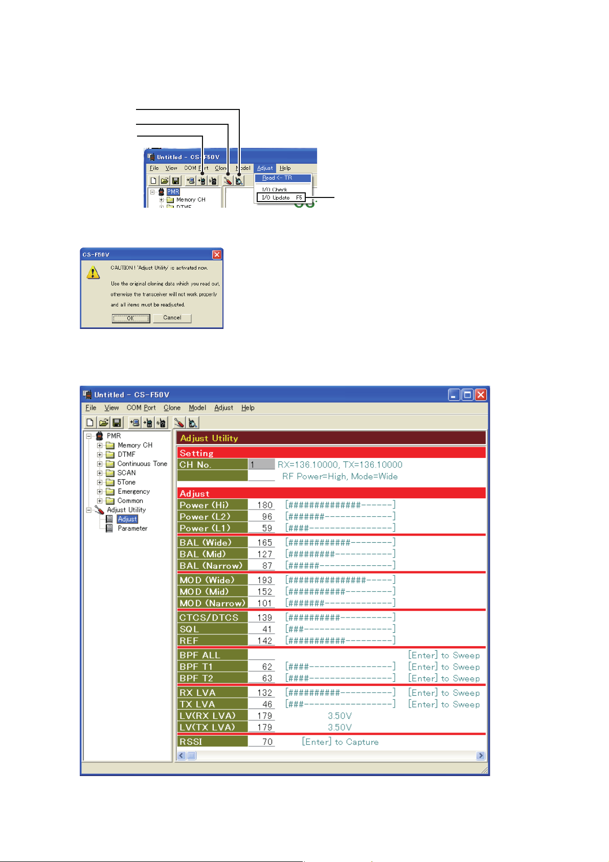
STARTING SOFTWARE ADJUSTMENT
¤
Connect the transceiver and PC with OPC-966/U. (see the page 5-3)
q
Turn the transceiver power ON.
w
Boot up Windows, and click the program group ‘CS-F50V’
e
CS-F50V’s window appears. (Or click the shortcut
Click [Adjust Read] button.
r
[I/O Check]
[Adjust Read]
[Clone Write]
The 'CAUTION' dialog appears. Click [OK].
t
‘CS-F50V’
in the ‘Programs’ folder of the [Start] menu, then
on the desktop.)
[I/O Update F5]
The adjustment window shows transceiver’s condition and adjustment items as below.
y
Set or modify adjustment data as specifi ed in the guidances (pages 5-4 to 5-12).
u
* This screen is an example only. Each transceiver has its own specific values for each setting.
When the adjustment is completed, click [Clone Write] button.
i
5 - 2
Page 17
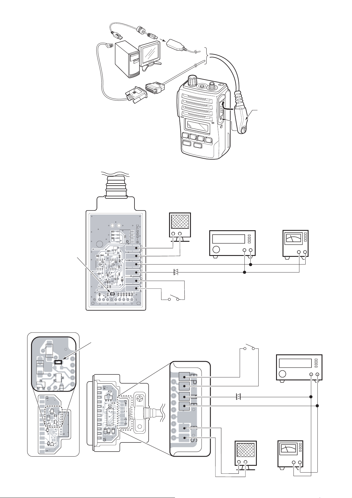
▄
PC CONNECTIONS
to an RS-232C port
RS-232C cable
(straight)
▄
JIG CABLES
OPC-966U
(USB type Cloning cable)
PC
JIG CABLE
OPC-966U (USB type)
JIG CABLE
C type)
OPC-966
(RS-232
EXT. SPEAKER
(1 W/8 Ω)
CAUTION: Attach the [SP
MIC] jack snugly, but do
not overtighten.
An overtightened jack will
damage the connector
pins in the transceiver.
Add a jumper wire here
GND
SP
GND
MIC
GND
PTT
Add a jumper wire here
OPC-966
(RS-232C type Cloning cable)
+−
+
4.7 µF
PTT SWITCH
AUDIO GENERATOR
(300–3000 Hz/1–500 mV)
+−
<SETTING>
Frequency
: 1 kHz
Level : 150 mV rms
PTT SWITCH
PTTE
PTT
MIC
MICE
(300–3000 Hz/1–500 mV)
+
4.7 µF
AC MILLIVOLTMETER
(10 mV to 10 V)
+−
SETTING;
Freq.
: 1 kHz
Level : 150 mV rms
AUDIO GENERATOR
+−
5 - 3
EXT. SPEAKER
(1 W/8 Ω)
+−
GND
SP
AC
MILLIVOLT-
METER
(10 mV to 10 V)
+−
Page 18

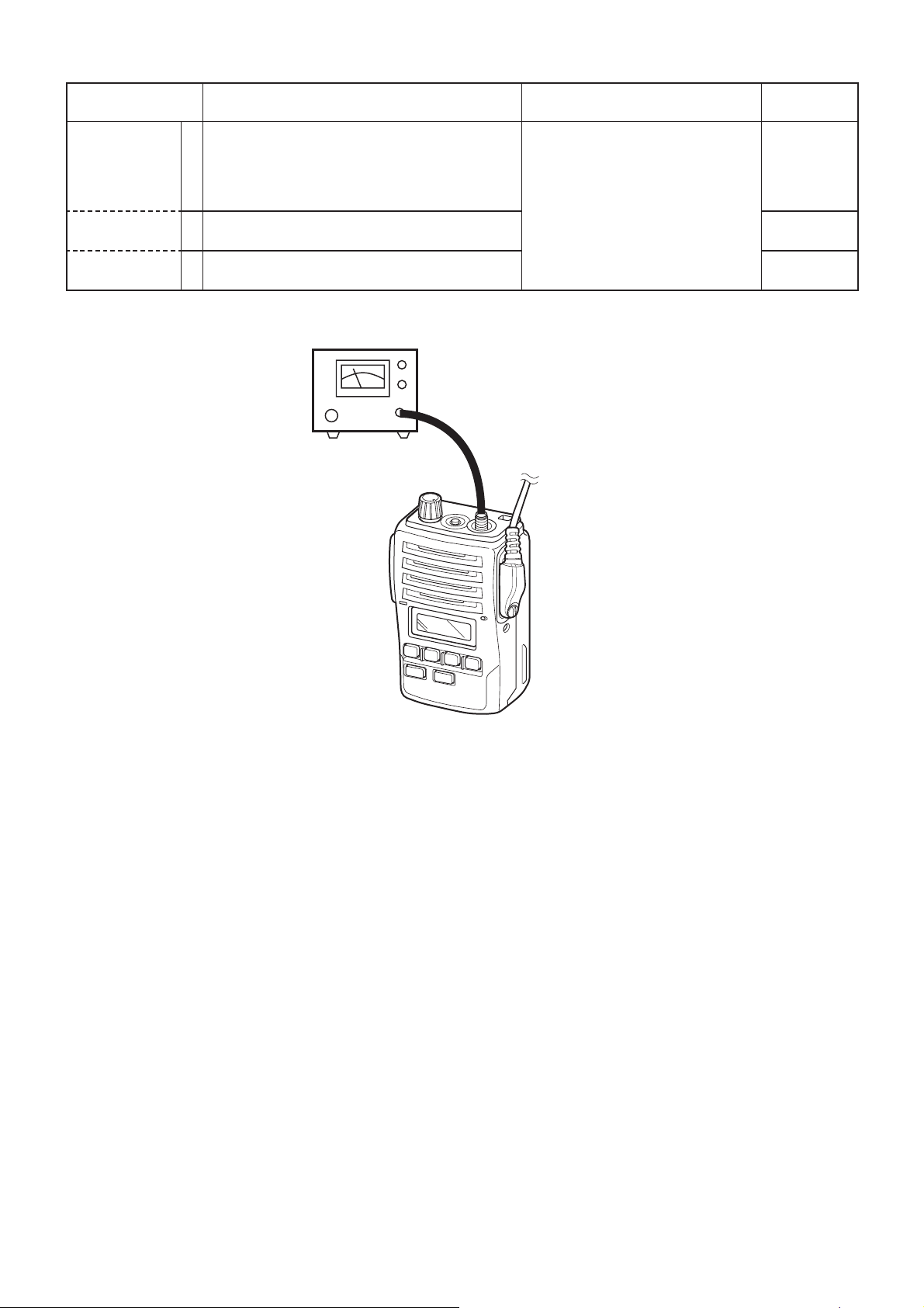
5-2 FREQUENCY ADJUSTMENT
Select an adjustment item using [↑] / [↓] keys, then set to the specifi ed value using [←] / [→] keys on the connected PC’s keyboard.
ADJUSTMENT
[ADJUST ITEM]
PLL LOCK
VOLTAGE
[RX LVA]
[TX LVA] 2 •
1• • Channel : 1-1
CONVENIENT:
1: Set the Lock voltage preset ([RX LVA] and [TX LVA]) to “179.”
2: Push the [ENTER] key on the connected PC’s keyboard.
PLL LOCK
VOLTAGE
(verify)
1• • Channel : 1-13
2• • Channel : 1-13
•
•
ADJUSTMENT CONDITION OPERATION VALUE
Click [I/O Update (F5)] in the [Adjust]
Receiving
Channel : 1-1
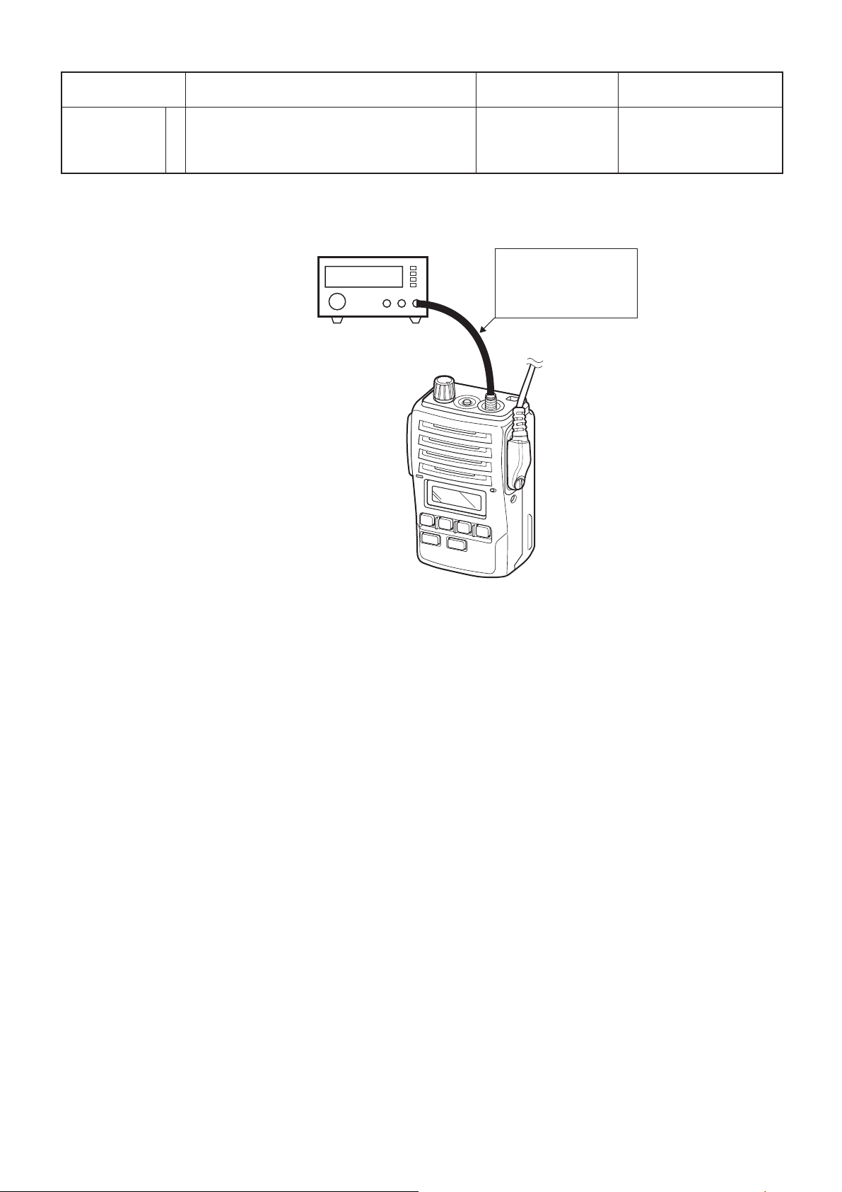
Connect an RF Power Meter to the
antenna connector.
Transmitting
The “
PLL LOCK VOLTAGE”
Receiving
Transmitting
RF POWER METER
(10 W/50 Ω)
menu (see the page 5-2), then check
the “LVIN” item on the I/O check window as below.
can be adjusted automatically.
Click [I/O Update (F5)] in the [Adjust]
menu (see the page 5-2), then check
the “LVIN” item on the I/O check window as below.
3.5 V
3.5 V
0.9–1.5 V
(Verify)
0.9–1.5 V
(Verify)
• I/O CHECK WINDOW
Lock Voltage
Check
* This screen is an example only. Each transceiver has its own specific values for each setting.
5 - 4
Page 19

5-2 FREQUENCY ADJUSTMENT (continued)
Select an adjustment item using [↑] / [↓] keys, then set to the specifi ed value using [←] / [→] keys on the connected PC’s keyboard.
ADJUSTMENT
[ADJUST ITEM]
REFERENCE
FREQUENCY
[REF]
1 • Channel : 1-2
•
•
ADJUSTMENT CONDITION OPERATION VALUE
Loosely couple a Frequency Counter to
Connect an RF Power Meter to the
the antenna connector.
antenna connector.
Transmitting
FREQUENCY COUNTER
(0.1–300 MHz)
RF POWER METER
(10 W/50 Ω)
174.000 MHz
(Loose Coupling)
5 - 5
Page 20
5-3 TRANSMIT ADJUSTMENT
Select an adjustment item using [↑] / [↓] keys, then set to the specifi ed value using [←] / [→] keys on the connected PC’s keyboard.
ADJUSTMENT
[ADJUST ITEM]
TRANSMIT
OUTPUT
POWER
(Hight)
[Hi]
(Low2)
[L2]
(Low1)
[L1]
1 • Channel : 1-3
•
Transmitting
•
2
Channel : 1-4
•
Transmitting
•
3
Channel : 1-5
•
Transmitting
ADJUSTMENT CONDITION OPERATION VALUE
Connect an RF power meter to the
antenna connector.
RF POWER METER
(10 W/50 Ω)
5.0 W
2.0 W
1.0 W
5 - 6
Page 21
5-3 TRANSMIT ADJUSTMENT (continued)
Select an adjustment item using [↑] / [↓] keys, then set to the specifi ed value using [←] / [→] keys on the connected PC’s keyboard.
ADJUSTMENT
[ADJUST ITEM]
FM DEVIATION
(Narrow)
[MOD(Narrow])
(Middle)*
[MOD(Mid])
(Wide)
[MOD(Wide])
1 • Channel : 1-6
Connect an Audio Generator and an AC Millivolt-
•
meter to the JIG cable (see the page 5-3).
Transmitting
•
2• • Channel : 1-7
Transmitting
3••Channel : 1-8
Transmitting
*; [EUR], [EUR-01], [EUR-02] only
SETTING;
HPF : OFF
LPF : 20 kHz
De-emphasis : OFF
Detector : (P-P)/2
ADJUSTMENT CONDITION OPERATION VALUE
Connect an Modulation Ana-
±2.05 to 2.15 kHz
lyzer to the antenna connector
through an Attenuator.
±3.15 to 3.25 kHz
±4.05 to 4.15 kHz
MODULATION ANALYZER
(0.1–300 MHz)
ATTENUATOR
(30 dB/10 W)
5 - 7
Page 22

5-3 TRANSMIT ADJUSTMENT (continued)
Select an adjustment item using [↑] / [↓] keys, then set to the specifi ed value using [←] / [→] keys on the connected PC’s keyboard.
ADJUSTMENT
[ADJUST ITEM]
MODULATION
BALANCE
(Narrow)
1•
Channel : 1-9
•
No audio signals are applied to the JIG cable.
•
Transmitting
[BAL(Narrow])
(Middle)*
[BAL(Mid])
(Wide)
[BAL(Wide])
2• • Channel : 1-10
Transmitting
3••Channel : 1-11
Transmitting
*; [EUR], [EUR-01], [EUR-02] only
ADJUSTMENT CONDITION OPERATION VALUE
Connect an Oscilloscope to the
detect output terminal of the
Set to the square
wave form
Modulation Analyzer.
OSCILLOSCOPE
(DC to 10 kHz)
MODULATION ANALYZER
(0.1–300 MHz)
SETTING;
HPF : OFF
LPF : 20 kHz
De-emphasis : OFF
Detector : (P-P)/2
ATTENUATOR
(30 dB/10 W)
(Detect output)
5 - 8
Page 23

5-3 TRANSMIT ADJUSTMENT (continued)
Select an adjustment item using [↑] / [↓] keys, then set to the specifi ed value using [←] / [→] keys on the connected PC’s keyboard.
ADJUSTMENT
[ADJUST ITEM]
CTCSS/DTCS
DEVIATION
[CTCSS/DTCS]
SETTING;
HPF : OFF
LPF : 20 kHz
De-emphasis : OFF
Detector : (P-P)/2
1 • Channel : 1-12
•
No audio signals are applied to the JIG cable.
•
Transmitting
ADJUSTMENT CONDITION OPERATION VALUE
Connect a Modulation Analyzer
±0.66 to 0.70 kHz
to the antenna connector through
an Attenuator.
MODULATION ANALYZER
(0.1–300 MHz)
ATTENUATOR
(30 dB/10 W)
5 - 9
Page 24

5-4 RECEIVE ADJUSTMENT
Select an adjustment item using [↑] / [↓] keys, then set to the specifi ed value using [←] / [→] keys on the connected PC’s keyboard.
ADJUSTMENT
[ADJUST ITEM]
RECEIVE
SENSITIVITY
[BPF T1]
1•
Channel : 1-13
•
Connect a Standard Signal Generator to the
antenna connector.
•
Receiving
[BPF T2] 2 Put the cursor on the [BPF T2],
CONVENIENT:
RECEIVE SENSITIVITY can be adjusted totally. Put the cursor on the [BPF ALL], and push the return key.
ADJUSTMENT CONDITION OPERATION VALUE
Put the cursor on the [BPF T1],
and push the return key.
(Automatic
adjustment)
and push the return key.
STANDARD SIGNAL GENERATOR
SETTING;
Modulation : 1 kHz
Deviation : 3.5 kHz
Level : +20 dBµ
(1–300 MHz)
CAUTION:
DO NOT transmit while
an SSG is connected to
the antenna connector.
5 - 10
Page 25

5-4 RECEIVE ADJUSTMENT (continued)
Select an adjustment item using [↑] / [↓] keys, then set to the specifi ed value using [←] / [→] keys on the connected PC’s keyboard.
ADJUSTMENT
[ADJUST ITEM]
S-METER
[S-METER]
(S6 LEVEL)
[S-METER]
(S1 LEVEL)
NOTE:
be adjusted properly.
1•
Channel : 1-14
•
Connect a Standard Signal Generator to the
antenna connector.
•
Set the SSG output level to “+13 dBµ (–94 dBm).”
•
Receiving
2•
Set the SSG output level to “–12 dBµ (–119 dBm).”
•
Receiving
ADJUSTMENT CONDITION OPERATION VALUE
“RECEIVE SENSITIVITY” must be adjusted before “S-METER.” Otherwise, “S-METER” will not
Push the return key to set the S6
level.
(Automatic
adjustment)
Push the return key to set the S1
level.
STANDARD SIGNAL GENERATOR
SETTING;
Modulation : 1 kHz
Deviation : 3.5 kHz
Level : +13 dBµ (S6 level)
−12 dBµ (S1 level)
(1–300 MHz)
CAUTION:
DO NOT transmit while
an SSG is connected to
the antenna connector.
5 - 11
Page 26
5-4 RECEIVE ADJUSTMENT (continued)
Select an adjustment item using [↑] / [↓] keys, then set to the specifi ed value using [←] / [→] keys on the connected PC’s keyboard.
ADJUSTMENT
[ADJUST ITEM]
SQUELCH
[SQL]
1 • Channel : 1-15
•
Connect a Standard Signal Generator to the
antenna connector.
ADJUSTMENT CONDITION OPERATION VALUE
Set the [SQL] value to close
–
squelch. Then set [SQL]
value at the point where the
audio signals just appear.
STANDARD SIGNAL GENERATOR
SETTING;
Modulation : 1 kHz
Deviation : 3.5 kHz
Level : −15 dBµ
(1–300 MHz)
CAUTION:
DO NOT transmit while
an SSG is connected to
the antenna connector.
5 - 12
Page 27

SECTION 6 PARTS LIST
[FRONT UNIT]
REF ORDER
NO. NO.
IC401 1140010191 S.IC HD64F2268TF20V T 22.9/28
IC403 1110005340 S.IC NJM12902V-TE1 T 16.9/42.9
IC405 1110006770 S.IC TDA8547TS/N T 25.8/53.2
IC406 1130011741 S.IC TC7W66FK (TE85L,F) T 8.1/42.4
IC407 1110005330 S.IC NJM12904V-TE1 T 7.1/31.6
IC408 1110006260 S.IC BD5242G-TR T 32/18.5
IC409 1130012690 S.IC HN58X24256FPIE (SOP8) T 10.1/17.8
IC410 1130011760 S.IC CD4094BPWR T 40.6/36.3
IC411 1130013240 S.IC TC75S51FU (TE85L,F) T 6.2/21.3
Q401 1550000090 S.FET RSQ035P03TR T 36.3/43.7
Q402 1590003800 S.TR KTC811U-GR-RTK/P T 35/39.6
Q406 1590003790 S.TR KRC404E RTK/P T 20.9/50.7
Q407 1590003780 S.TR KRA304E-RTK/P T 42/31.3
Q408 1590003790 S.TR KRC404E RTK/P T 26/39.2
Q409 1590002370 S.TR XP4111 (TX) T 39.2/29
Q411 1590003790 S.TR KRC404E RTK/P T 29.3/18.8
Q412 1590003780 S.TR KRA304E-RTK/P T 14.3/17.6
Q413 1560001330 S.FET RSR025N03 B 32.3/53
Q414 1590003790 S.TR KRC404E RTK/P T 40.8/41.8
Q415 1530003091 S.TR 2SC4213-B (TE85R,F) B 23.9/51.1
D401 1790001250 S.DIO MA2S111-(TX) T 35.4/23.1
D402 1790001250 S.DIO MA2S111-(TX) T 35.1/18.1
D403 1790001250 S.DIO MA2S111-(TX) T 15/16
D404 1790001260 S.DIO MA2S077-(TX) T 37/24
D406 1790001250 S.DIO MA2S111-(TX) T 36.5/36
D407 1790001250 S.DIO MA2S111-(TX) T 9/23.1
X401 6050011720 S.XTL CR-764 (19.6608 MHz) T 42.6/18.8
R401 7030007290 S.RES ERJ2GEJ 222 X (2.2 k) T 9.9/44.3
R402 7030005060 S.RES ERJ2GEJ 333 X (33 k) T 10.7/52.2
R403 7030005120 S.RES ERJ2GEJ 102 X (1 k) T 34.3/22.3
R404 7030005120 S.RES ERJ2GEJ 102 X (1 k) T 35.8/20.2
R405 7030007340 S.RES ERJ2GEJ 153 X (15 k) T 9.6/35.1
R406 7030005210 S.RES ERJ2GEJ 822 X (8.2 k) T 10.5/36.4
R407 7030005230 S.RES ERJ2GEJ 334 X (330 k) T 7.4/27.3
R408 7030005090 S.RES ERJ2GEJ 104 X (100 k) T 6.8/36.3
R409 7030005090 S.RES ERJ2GEJ 104 X (100 k) T 36.3/21.4
R410 7030005090 S.RES ERJ2GEJ 104 X (100 k) T 9.8/39.6
R411 7030005090 S.RES ERJ2GEJ 104 X (100 k) T 13.8/20.4
R412 7030005090 S.RES ERJ2GEJ 104 X (100 k) T 29.2/13.9
R413 7030005600 S.RES ERJ2GEJ 273 X (27 k) T 27.3/13.7
R414 7030005600 S.RES ERJ2GEJ 273 X (27 k) T 36.9/13.6
R415 7030005100 S.RES ERJ2GEJ 154 X (150 k) T 39/23.4
R416 7030005100 S.RES ERJ2GEJ 154 X (150 k) T 33.4/20.9
R417 7030005170 S.RES ERJ2GEJ 474 X (470 k) T 17.5/19
R418 7030005170 S.RES ERJ2GEJ 474 X (470 k) T 5.3/16.3
R420 7030005600 S.RES ERJ2GEJ 273 X (27 k) T 28.7/37.2
R421 7030005090 S.RES ERJ2GEJ 104 X (100 k) T 29.9/36.5
R422 7030005090 S.RES ERJ2GEJ 104 X (100 k) T 30.2/35.6
R423 7030005090 S.RES ERJ2GEJ 104 X (100 k) T 31.5/36.5
R426 7030005160 S.RES ERJ2GEJ 105 X (1 M) T 12.3/35.3
R427 7030005240 S.RES ERJ2GEJ 473 X (47 k) T 14.5/37.8
R428 7030005240 S.RES ERJ2GEJ 473 X (47 k) T 13.8/36.9
R429 7030005040 S.RES ERJ2GEJ 472 X (4.7 k) T 12.3/36.2
R430 7030005050 S.RES ERJ2GEJ 103 X (10 k) T 12.9/40.2
R432 7030005090 S.RES ERJ2GEJ 104 X (100 k) T 14.5/39.6
R433 7030005090 S.RES ERJ2GEJ 104 X (100 k) T 12.2/42.1
R434 7030005000 S.RES ERJ2GEJ 471 X (470) B 35/55.4
R437 7030005120 S.RES ERJ2GEJ 102 X (1 k) T 32.9/38.4
R438 7030005090 S.RES ERJ2GEJ 104 X (100 k) T 34.7/37.7
R439 7030007290 S.RES ERJ2GEJ 222 X (2.2 k) T 36.8/40.2
R440 7030005090 S.RES ERJ2GEJ 104 X (100 k) T 36.1/33.4
R441 7030005070 S.RES ERJ2GEJ 683 X (68 k) T 37.3/33.7
R445 7030004980 S.RES ERJ2GEJ 101 X (100) B 32.3/55.2
R446 7030005090 S.RES ERJ2GEJ 104 X (100 k) B 30.1/52.1
R455 7030005000 S.RES ERJ2GEJ 471 X (470) T 43.2/27.8
R456 7030004980 S.RES ERJ2GEJ 101 X (100) T 43.2/28.7
R457 7030005000 S.RES ERJ2GEJ 471 X (470) B 45.2/48.4
R458 7030005120 S.RES ERJ2GEJ 102 X (1 k) B 43.9/49.9
R461 7030008300 S.RES ERJ2GEJ 184 X (180 k) T 33.2/32.4
R462 7030005720 S.RES ERJ2GEJ 563 X (56 k) T 32/33.2
R463 7030005220 S.RES ERJ2GEJ 223 X (22 k) T 31.1/33.6
R464 7030005220 S.RES ERJ2GEJ 223 X (22 k) T 31.5/34.8
R465 7030005050 S.RES ERJ2GEJ 103 X (10 k) T 33.2/34.7
R466 7030005240 S.RES ERJ2GEJ 473 X (47 k) T 23.9/41.3
R467 7030005240 S.RES ERJ2GEJ 473 X (47 k) T 23/41.3
R468 7030005240 S.RES ERJ2GEJ 473 X (47 k) T 21.2/41.3
R469 7030005040 S.RES ERJ2GEJ 472 X (4.7 k) T 18.5/39
R470 7030005240 S.RES ERJ2GEJ 473 X (47 k) T 19.7/38.6
R471 7030005110 S.RES ERJ2GEJ 224 X (220 k) T 34.5/24.7
R472 7030005090 S.RES ERJ2GEJ 104 X (100 k) T 33.6/24.7
R473 7030005240 S.RES ERJ2GEJ 473 X (47 k) T 32.7/24.7
R474 7030005220 S.RES ERJ2GEJ 223 X (22 k) T 31.8/24.3
R475 7030005050 S.RES ERJ2GEJ 103 X (10 k) T 35.7/24.8
R476 7030005070 S.RES ERJ2GEJ 683 X (68 k) T 23.3/46.1
R477 7030005070 S.RES ERJ2GEJ 683 X (68 k) T 21.7/46.1
R478 7030005070 S.RES ERJ2GEJ 683 X (68 k) T 21.2/44.6
R479 7030005070 S.RES ERJ2GEJ 683 X (68 k) T 18.3/46.2
R480 7030005070 S.RES ERJ2GEJ 683 X (68 k) T 12.5/45
R482 7030005090 S.RES ERJ2GEJ 104 X (100 k) T 36.5/32
R483 7030005090 S.RES ERJ2GEJ 104 X (100 k) T 15.8/21.8
DESCRIPTION
M.
H/V
LOCATION
[FRONT UNIT]
REF ORDER
NO. NO.
R484 7030005090 S.RES ERJ2GEJ 104 X (100 k) T 15.6/20.9
R485 7030005090 S.RES ERJ2GEJ 104 X (100 k) T 14.2/21.7
R486 7410001130 S.ARY EXB28V102JX T 13.6/24.7
R487 7030005090 S.RES ERJ2GEJ 104 X (100 k) T 33.9/23.5
R488 7030005090 S.RES ERJ2GEJ 104 X (100 k) T 31.9/31.3
R489 7030005050 S.RES ERJ2GEJ 103 X (10 k) T 32.9/31.2
R490 7030005050 S.RES ERJ2GEJ 103 X (10 k) T 33.8/31.2
R491 7030005530 S.RES ERJ2GEJ 100 X (10) T 38.5/18.4
R492 7030005160 S.RES ERJ2GEJ 105 X (1 M) T 38.5/20.1
R493 7030008010 S.RES ERJ2GEJ 123 X (12 k) T 37.6/19.3
R494 7030008010 S.RES ERJ2GEJ 123 X (12 k) T 38.4/25.8
R495 7030008010 S.RES ERJ2GEJ 123 X (12 k) T 37.2/20.5
R496 7030005050 S.RES ERJ2GEJ 103 X (10 k) T 11.3/22.8
R497 7030005050 S.RES ERJ2GEJ 103 X (10 k) T 11.9/21.9
R500 7030005090 S.RES ERJ2GEJ 104 X (100 k) T 29/21.1
R501 7030005090 S.RES ERJ2GEJ 104 X (100 k) T 28.1/20.3
R502 7030010080 S.RES ERJ2RHD 104 X (100 k) T 38.4/14.3
R503 7030010080 S.RES ERJ2RHD 104 X (100 k) T 39.3/14.3
R506 7030007300 S.RES ERJ2GEJ 332 X (3.3 k) T 7.6/23.9
R507 7030005600 S.RES ERJ2GEJ 273 X (27 k) T 7.6/24.8
R508 7030007290 S.RES ERJ2GEJ 222 X (2.2 k) T 5/25.7
R509 7030005050 S.RES ERJ2GEJ 103 X (10 k) T 26.2/18.9
R511 7030005090 S.RES ERJ2GEJ 104 X (100 k) T 9.6/33.2
R512 7030005090 S.RES ERJ2GEJ 104 X (100 k) T 6.2/26.9
R513 7030009290 S.RES ERJ2GEJ 562 X (5.6 k) T 7.7/36.3
R515 7520000270 S.POS PRG21BC4R7MM1RA T 34.2/46.7
R516 7030007290 S.RES ERJ2GEJ 222 X (2.2 k) T 37/38.7
R517 7030008010 S.RES ERJ2GEJ 123 X (12 k) T 31.1/50.8
R518 7030005050 S.RES ERJ2GEJ 103 X (10 k) T 30.7/48.7
R519 7030005050 S.RES ERJ2GEJ 103 X (10 k) T 30.4/53.8
R520 7030005050 S.RES ERJ2GEJ 103 X (10 k) T 30.4/52.2
R521 7030005090 S.RES ERJ2GEJ 104 X (100 k) T 30.5/55.1
R522 7030005100 S.RES ERJ2GEJ 154 X (150 k) T 30.2/49.6
R523 7030005120 S.RES ERJ2GEJ 102 X (1 k) T 21.1/52.3
R524 7030005090 S.RES ERJ2GEJ 104 X (100 k) T 21.1/53.7
R525 7030005090 S.RES ERJ2GEJ 104 X (100 k) T 21.5/54.9
R526 7030007340 S.RES ERJ2GEJ 153 X (15 k) T 5/24.8
R527 7030005230 S.RES ERJ2GEJ 334 X (330 k) T 5/23.9
R528 7030009140 S.RES ERJ2GEJ 272 X (2.7 k) T 5/19.6
R529 7030005050 S.RES ERJ2GEJ 103 X (10 k) T 6.6/19.6
R530 7030005160 S.RES ERJ2GEJ 105 X (1 M) T 10.4/24.2
R532 7030005700 S.RES ERJ2GEJ 274 X (270 k) T 36.7/41.5
R533 7030005050 S.RES ERJ2GEJ 103 X (10 k) T 35.1/41.5
R534 7030005170 S.RES ERJ2GEJ 474 X (470 k) T 36.9/34.9
R535 7030005070 S.RES ERJ2GEJ 683 X (68 k) T 11.9/33.5
R537 7030005050 S.RES ERJ2GEJ 103 X (10 k) B 22/50.7
R538 7030005060 S.RES ERJ2GEJ 333 X (33 k) B 22/52.3
R539 7030005040 S.RES ERJ2GEJ 472 X (4.7 k) B 25.5/52.8
R541 7030005050 S.RES ERJ2GEJ 103 X (10 k) T 10.3/53.4
C401 4030017460 S.CER ECJ0EB1E102K T 10.7/51.3
C402 4030017460 S.CER ECJ0EB1E102K T 15/20
C403 4030017460 S.CER ECJ0EB1E102K T 31/22.6
C404 4030017460 S.CER ECJ0EB1E102K T 10.3/43.1
C405 4030017760 S.CER ECJ0EB1H222K T 10.5/34.8
C406 4030018110 S.CER ECJ0EB1H272K T 9.6/36.7
C407 4030017430 S.CER ECJ0EC1H101J T 7.4/26.4
C408 4030016930 S.CER ECJ0EB1A104K T 29.6/37.7
C409 4030016930 S.CER ECJ0EB1A104K T 27.8/37.6
C410 4030016930 S.CER ECJ0EB1A104K T 30.5/37.7
C411 4030016930 S.CER ECJ0EB1A104K T 31.7/37.4
C412 4030016930 S.CER ECJ0EB1A104K T 36.7/19.3
C413 4030016930 S.CER ECJ0EB1A104K T 38.1/24.6
C414 4030017640 S.CER ECJ0EC1H150J T 38.1/21.4
C415 4030016790 S.CER ECJ0EB1C103K T 34.6/20.2
C416 4030017630 S.CER ECJ0EC1H120J T 39.4/19.2
C417 4030017580 S.CER ECJ0EC1H060C T 39.4/20.8
C418 4030016930 S.CER ECJ0EB1A104K T 39/24.6
C419 4550006050 S.TAN TEESVA 0J 106M8R T 24.6/16.9
C420 4030016930 S.CER ECJ0EB1A104K T 24.9/18.5
C421 4030016930 S.CER ECJ0EB1A104K T 13.5/35.7
C423 4030018890 S.CER ECJ0EB0J224K T 12.9/39.2
C425 4030017440 S.CER ECJ0EC1H221J T 14.5/38.7
C426 4030017460 S.CER ECJ0EB1E102K B 35.6/54.2
C427 4550007080 S.TAN TEESVA 1C 106M8R T 40.6/44.3
C428 4030016930 S.CER ECJ0EB1A104K T 37.6/47
C429 4030017460 S.CER ECJ0EB1E102K T 36.7/47
C430 4030017460 S.CER ECJ0EB1E102K T 34.7/36.8
C431 4030016790 S.CER ECJ0EB1C103K T 32.9/39.3
C432 4030017460 S.CER ECJ0EB1E102K T 38.9/42.7
C435 4550006760 S.TAN TEESVB21A336M8R T 18.5/54.3
C437 4030018860 S.CER ECJ0EB0J105K B 34.1/55.4
C441 4030016780 S.CER ECJ0EB1C153K T 23.4/42.9
C442 4030016930 S.CER ECJ0EB1A104K T 22.1/41.3
C443 4030017740 S.CER ECJ0EB1E821K T 22.2/42.5
C444 4030016930 S.CER ECJ0EB1A104K T 19.7/39.5
C445 4030017460 S.CER ECJ0EB1E102K T 33.2/33.8
C446 4030017460 S.CER ECJ0EB1E102K T 22.5/45.2
C447 4030017760 S.CER ECJ0EB1H222K T 20.1/45.7
C448 4030017690 S.CER ECJ0EC1H121J T 22.5/44.3
C449 4030017770 S.CER ECJ0EB1E332K T 13.7/45.7
C450 4030017420 S.CER ECJ0EC1H470J T 12.2/43.7
C461 4030017420 S.CER ECJ0EC1H470J T 39/22.5
C462 4030017420 S.CER ECJ0EC1H470J T 32/21
C463 4030017420 S.CER ECJ0EC1H470J T 17.5/19.9
C464 4030017420 S.CER ECJ0EC1H470J T 4.4/16.3
C465 4030017420 S.CER ECJ0EC1H470J T 26.4/13.7
DESCRIPTION
M.=Mounted side (T: Mounted on the Top side, B: Mounted on the Bottom side)
6 - 1
M.
S.=Surface mount
H/V
LOCATION
Page 28

[FRONT UNIT]
REF ORDER
NO. NO.
C466 4030017420 S.CER ECJ0EC1H470J T 36.9/14.5
C467 4030017420 S.CER ECJ0EC1H470J T 30.5/13.1
C468 4030017420 S.CER ECJ0EC1H470J T 40.4/11.5
C473 4030016790 S.CER ECJ0EB1C103K T 38.1/15.9
C474 4030018860 S.CER ECJ0EB0J105K T 5/26.6
C475 4030017460 S.CER ECJ0EB1E102K T 33/45.4
C476 4030017460 S.CER ECJ0EB1E102K T 29.9/21.9
C477 4030017420 S.CER ECJ0EC1H470J T 33.3/44.1
C478 4030017420 S.CER ECJ0EC1H470J T 33.5/41.9
C479 4030017460 S.CER ECJ0EB1E102K T 27.8/17.7
C481 4030017460 S.CER ECJ0EB1E102K T 6.4/38.1
C482 4030017460 S.CER ECJ0EB1E102K T 11.8/41.2
C483 4030017460 S.CER ECJ0EB1E102K T 38.8/41.8
C485 4030017460 S.CER ECJ0EB1E102K T 33.7/48
C486 4030017460 S.CER ECJ0EB1E102K T 32.1/47.5
C487 4030017460 S.CER ECJ0EB1E102K T 34.4/35.9
C488 4030017460 S.CER ECJ0EB1E102K T 22.1/43.4
C489 4030017460 S.CER ECJ0EB1E102K T 9.9/30.9
C490 4030017460 S.CER ECJ0EB1E102K T 40.3/27
C491 4030017460 S.CER ECJ0EB1E102K T 37.3/37.3
C492 4030017460 S.CER ECJ0EB1E102K T 6.8/18.2
C493 4030016930 S.CER ECJ0EB1A104K T 17.4/34.7
C494 4030017460 S.CER ECJ0EB1E102K T 39.6/67.3
C495 4030017460 S.CER ECJ0EB1E102K T 10/40.5
C496 4550006760 S.TAN TEESVB21A336M8R T 13.2/54.7
C497 4030018390 S.CER ECJ0EB1A563K T 8.1/37.9
C498 4030017430 S.CER ECJ0EC1H101J T 10.5/33.2
C499 4030017420 S.CER ECJ0EC1H470J T 15.4/36.9
C500 4030016930 S.CER ECJ0EB1A104K T 9.3/37.9
C501 4030017730 S.CER ECJ0EB1E471K T 35.1/13.2
C502 4030016930 S.CER ECJ0EB1A104K T 31.9/49.6
C503 4030018860 S.CER ECJ0EB0J105K T 32.3/48.7
C504 4550007080 S.TAN TEESVA 1C 106M8R T 40.6/46.4
C505 4030016960 S.CER ECJ0EB1C183K T 6.3/25.3
C506 4030016960 S.CER ECJ0EB1C183K T 6.3/23.4
C507 4030017730 S.CER ECJ0EB1E471K T 5/23
C508 4030017730 S.CER ECJ0EB1E471K T 11.3/24.2
C510 4550000460 S.TAN TEESVA 1C 105M8R T 23.5/48.6
C512 4030018860 S.CER ECJ0EB0J105K B 22.3/49.5
C513 4030018860 S.CER ECJ0EB0J105K B 25.9/51.5
DESCRIPTION
M.
H/V
LOCATION
[VR UNIT]
REF ORDER
NO. NO.
R601 7210003130 VAR TP76N97N-13F-10KA-2497
W601 8900012340 CBL OPC-1260
DESCRIPTION
M.
H/V
LOCATION
[CONNECT UNIT]
REF ORDER
NO. NO.
D701 1790001810 S.VSR AVR-M1005C080MTABB T 9.5/31.8
D702 1790001810 S.VSR AVR-M1005C080MTABB T 9.2/32.8
D703 1790001810 S.VSR AVR-M1005C080MTABB T 4.7/32.3
D704 1790001810 S.VSR AVR-M1005C080MTABB T 3.4/32
D705 1790001810 S.VSR AVR-M1005C080MTABB T 4.8/20.7
R701 7410001130 S.ARY EXB28V102JX T 6.5/32.5
C701 4030017460 S.CER ECJ0EB1E102K T 4.6/9.9
C702 4030017460 S.CER ECJ0EB1E102K T 4.4/14.2
C704 4030017460 S.CER ECJ0EB1E102K T 3.9/17.1
J1 6510026140 S.CNR 11FH-SM1-TB (LF) (SN) T 3.6/37.1
EP701 6910016330 S.BEA MMZ1005S 601CT-S T 6.4/9.9
EP702 6910016330 S.BEA MMZ1005S 601CT-S T 4.8/12.9
EP703 6910016330 S.BEA MMZ1005S 601CT-S T 4.9/16.5
EP704 6910016330 S.BEA MMZ1005S 601CT-S T 4.4/18.4
EP705 6910016330 S.BEA MMZ1005S 601CT-S T 4.8/19.4
DESCRIPTION
M.=Mounted side (T: Mounted on the Top side, B: Mounted on the Bottom side)
S.=Surface mount
M.
H/V
LOCATION
J401 6510026130 S.CNR IMSA-9681S-36Y900 T 30.9/6.2
J402 6510023831 S.CNR (G) SM04B-SRSS-TB(LF)(SN) T 34.9/52.5
J403 6510026140 S.CNR 11FH-SM1-TB (LF) (SN) T 29/43.5
DS401 5030002730 LCD L3-0048TAY-5
DS402 5040002420 S.LED SML-310MT T86 B 13.5/16.1
DS403 5040002420 S.LED SML-310MT T86 B 32.7/15.3
DS404 5040002961 S.LED SML-A12MT T86J B 6.2/38
DS405 5040002961 S.LED SML-A12MT T86J B 42.8/38
DS406 5040002670 S.LED CL-165HR/YG B 45.3/50.2
MC401 7700002760 MIC EM6027P-46C33-G-01 <HOR>
S401 2260002840 SW SKHLLFA010
SP401 2510001330 SP 036D0803 <FG>
W401 8900016840 CBL OPC-1753 (P0.5,N36,L70) <TJM>
W402 7120000470 JMP ERDS2T0
W403 7120000470 JMP ERDS2T0
W404 8900017120 CBL OPC-1754 (P0.5,N11,L35) <TJM>
EP402 8930061530 LCT SRCN-2681-SP-N-W
6 - 2
Page 29

[MAIN UNIT]
REF ORDER
NO. NO.
IC1 1110003201 S.IC TA31136FNG (EL) B 19.1/9.1
IC2 1110002751 S.IC TA75S01F (TE85R,F) T 52.3/18.1
IC4 1140005991 S.IC MB15A02PFV1-G-BND-ERE1 B 28.7/24.1
IC5 1110005330 S.IC NJM12904V-TE1 T 34.3/9.3
IC6 1190000350 S.IC M62363FP-650C T 25.2/8.9
IC7 1190001860 S.IC EW-460-FT B 50.7/39.9
IC9 1110005350 S.IC NJM2870F05-TE1-#FZZB T 73.8/28.6
IC10 1110006221 S.IC AK2346P-E2/P T 18.9/25.1
IC11 1130009981 S.IC TC7W53FK (TE85L,F) T 25.2/29.2
IC12 1130011760 S.IC CD4094BPWR T 17.2/35.8
IC16 1110005330 S.IC NJM12904V-TE1 T 30/29.1
IC17 1130004201 S.IC TC4S66F (TE85R,F) T 29.5/35.7
IC18 1190002660 S.IC ISD4004-08MEYI
[C], [I], [F], [L] only B 13.1/36.5
IC19 1180002391 S.REG S-812C33AMC-C2N-G
[C], [I], [F], [L] only B 24.5/41
Q1 1560000841 S.FET 2SK1829 (TE85R,F) T 46.4/10.8
Q2 1580000731 S.FET 3SK293 (TE85L,F) T 47.3/8.2
Q3 1580000800 S.FET 3SK324UG-TL-E B 41.2/9.1
Q4 1530002601 S.TR 2SC4215-O (TE85R,F) B 23.9/4.1
Q6 1590001650 S.TR XP4601 (TX) B 5.9/26.7
Q7 1560001232 S.FET RD07MVS2-T112 T 59.8/21.9
Q8 1560001241 S.FET RD01MUS1-T113 T 60.2/28
Q9 1530003421 S.TR 2SC5110-O (TE85R,F) B 52.4/29
Q10 1530003311 S.TR 2SC5107-O (TE85R,F) B 47.9/21.9
Q11 1530003311 S.TR 2SC5107-O (TE85R,F) T 43.7/32.1
Q12 1530003311 S.TR 2SC5107-O (TE85R,F) B 47.6/29.5
Q13 1530002920 S.TR 2SC4226-T1 R25 B 45/22.4
Q14 1530002920 S.TR 2SC4226-T1 R25 B 43.9/29.9
Q15 1590001400 S.TR XP1214 (TX) T 45.8/26.2
Q16 1590003790 S.TR KRC404E RTK/P T 43.4/27
Q17 1530003900 S.TR KTC4075 BL-RTK/P B 47.4/37.1
Q18 1560000541 S.FET 2SK880-Y (T5RICOM,F) T 46.4/17.3
Q19 1530003900 S.TR KTC4075 BL-RTK/P B 26/15.9
Q21 1510001090 S.TR KTA2015Y-RTK/P B 52.8/36.5
Q22 1510001090 S.TR KTA2015Y-RTK/P B 31.9/37.9
Q23 1520000840 S.TR KTA1664Y-RTF/P B 72.1/25.4
Q24 1590003800 S.TR KTC811U-GR-RTK/P B 72.1/29.2
Q25 1590003780 S.TR KRA304E-RTK/P B 68.8/31.6
Q26 1550000090 S.FET RSQ035P03TR T 72.9/25.1
Q29 1590003790 S.TR KRC404E RTK/P B 54.6/39.7
Q30 1530003900 S.TR KTC4075 BL-RTK/P
[C], [I], [F], [L] only B 36.7/40.4
Q31 1520000840 S.TR KTA1664Y-RTF/P
D1 1790001670 S.DIO RB706F-40T106 B 55.5/12.3
D2 1750000581 S.DIO 1SV307 (TPH3,F) B 59.8/8.3
D4 1750000721 S.VCP HVC375BTRF-E T 50.2/5.6
D5 1750000581 S.DIO 1SV307 (TPH3,F) B 57/3.5
D6 1790001260 S.DIO MA2S077-(TX) T 59.9/7.9
D7 1790001240 S.DIO MA2S728-(TX) T 56.6/7.9
D8 1750000721 S.VCP HVC375BTRF-E T 54.6/5.6
D9 1750000711 S.VCP HVC350BTRF-E T 43.2/5.6
D10 1750000711 S.VCP HVC350BTRF-E T 38.8/5.6
D12 1790001250 S.DIO MA2S111-(TX) B 47.6/40.1
D14 1790001260 S.DIO MA2S077-(TX) B 51.8/23.7
D15 1790001260 S.DIO MA2S077-(TX) B 51.8/18
D16 1750000771 S.VCP HVC376BTRF-E B 40.6/20.5
D17 1750000771 S.VCP HVC376BTRF-E B 42.8/21.8
D18 1720000471 S.VCP 1SV239 (TPH3,F) T 37.9/21.5
D19 1750000771 S.VCP HVC376BTRF-E B 40.8/27.4
D20 1750000771 S.VCP HVC376BTRF-E B 40.8/28.8
D21 1750000721 S.VCP HVC375BTRF-E B 37.2/22.7
D22 1750000721 S.VCP HVC375BTRF-E B 37.2/29.4
D23 1790001250 S.DIO MA2S111-(TX) T 42.1/8.7
D24 1790001250 S.DIO MA2S111-(TX) B 32.5/29.2
D25 1790001250 S.DIO MA2S111-(TX) T 53.3/15
D26 1790000980 S.DIO MA742 (TX) B 28/1.8
FI1 2030000150 S.MLH FL-335 (46.350 MHz) B 32.4/5.8
FI2 2020002160 S.CER CFWKA450KFFA-R0 B 19.7/21
X1 6070000191 S.DCR CDBKB450KCAY24-R0 T 16.9/9.6
X2 6050011940 S.XTL CR-783 (15.3 MHz) B 28.4/33.4
X4 6050011730 S.XTL CR-765 (3.6864 MHz) B 16.6/29.6
L1 6200012780 S.COL 0.30-1.4-6TL 27.2N B 67.8/7
L2 6200012770 S.COL 0.26-1.1-7TR 24N B 63.4/5.5
L3 6200012470 S.COL 0.30-1.7-7TL 45.3N B 62/11.4
L4 6200012390 S.COL 0.30-0.92-3TR 5.8N B 67.4/13.4
L5 6200012470 S.COL 0.30-1.7-7TL 45.3N B 57.3/5.8
L6 6200005711 S.COL ELJRE 27NGFA B 56.5/7.9
L7 6200008090 S.COL LQW2BHN68NJ03L B 53.6/4.5
L8 6200008090 S.COL LQW2BHN68NJ03L B 50.9/4.5
L9 6200007750 S.COL LQW2BHN56NJ03L B 47.3/7.7
L11 6200007750 S.COL LQW2BHN56NJ03L B 41.3/5.2
L12 6200008090 S.COL LQW2BHN68NJ03L B 44.1/11.3
L13 6200007850 S.COL ELJNC R82K-F B 38.1/11.7
L14 6200005681 S.COL ELJRE 15NGFA B 47.8/12.1
L15 6200002861 S.COL NLV25T-4R7J B 57.2/9.8
L16 6200012400 S.COL 0.30-0.91-4TL 8.6N B 68.6/18.3
L17 6200013100 S.COL 0.45-1.5-5TL 18.3N B 67.3/21.4
L18 6200005701 S.COL ELJRE 22NGFA T 65.5/26.5
L19 6200005741 S.COL ELJRE 47NGFA B 54.4/29
L20 6200003590 S.COL EXCCL3225U1 B 71.9/21.4
L21 6200009181 S.COL ELJRE R10JFA T 47.8/21.4
L22 6200009181 S.COL ELJRE R10JFA B 47.7/27.6
DESCRIPTION
[B], [H], [E], [K], [C], [I], [F], [L] only
H/V
M.
LOCATION
B 41.1/39.7
[MAIN UNIT]
REF ORDER
NO. NO.
L24 6200003640 S.COL MLF1608E 100K-T B 41.4/24.4
L25 6200007760 S.COL LQW2BHN82NJ03L B 38.8/24.9
L26 6200008090 S.COL LQW2BHN68NJ03L B 37.8/31.6
L27 6200007170 S.COL MLF1608A 3R3K-T T 41/21.9
L28 6200007170 S.COL MLF1608A 3R3K-T T 40.4/25.1
L31 6200009181 S.COL ELJRE R10JFA T 58.8/4.8
L32 6200005721 S.COL ELJRE 33NGFA T 37.1/32.1
L33 6200004480 S.COL MLF1608D R82K-T B 27.3/12.7
L35 6200003540 S.COL MLF1608D R22K-T B 27.8/18.1
L37 6200003640 S.COL MLF1608E 100K-T B 40.8/30.1
L38 6200008090 S.COL LQW2BHN68NJ03L B 37.7/21
L39 6200007720 S.COL LQW2BHN33NJ03L B 37.9/27.7
L41 6200009181 S.COL ELJRE R10JFA T 41.3/30.9
L42 6200007170 S.COL MLF1608A 3R3K-T T 36.6/28.5
L43 6200007170 S.COL MLF1608A 3R3K-T T 36.6/25.1
R1 7030003490 S.RES ERJ3GEYJ 272 V (2.7 k) B 59.1/11.7
R2 7030005040 S.RES ERJ2GEJ 472 X (4.7 k) T 55.5/15.2
R3 7030005530 S.RES ERJ2GEJ 100 X (10) T 52.6/20.3
R4 7030005050 S.RES ERJ2GEJ 103 X (10 k) T 56.5/17
R5 7030005050 S.RES ERJ2GEJ 103 X (10 k) T 54.5/15.2
R6 7030005070 S.RES ERJ2GEJ 683 X (68 k) T 52.1/15.2
R7 7030005310 S.RES ERJ2GEJ 124 X (120 k) T 50.8/15.7
R8 7030005110 S.RES ERJ2GEJ 224 X (220 k) T 54.5/17
R9 7030004980 S.RES ERJ2GEJ 101 X (100) T 55/18.3
R10 7030005030 S.RES ERJ2GEJ 152 X (1.5 k) T 54.2/20.5
R11 7030005090 S.RES ERJ2GEJ 104 X (100 k) T 53.4/5.1
R12 7030005530 S.RES ERJ2GEJ 100 X (10) T 49.3/8.7
R13 7030005090 S.RES ERJ2GEJ 104 X (100 k) T 51.4/5.1
R14 7030005050 S.RES ERJ2GEJ 103 X (10 k) T 52.4/7.7
R15 7030005310 S.RES ERJ2GEJ 124 X (120 k) T 47.7/4.4
R16 7030008280 S.RES ERJ2GEJ 271 X (270) T 45.4/5.1
R17 7030004970 S.RES ERJ2GEJ 470 X (47) B 49.1/9.3
R18 7030009320 S.RES ERJ2GEJ 4R7 X (4.7) B 50.3/9.2
R19 7030005090 S.RES ERJ2GEJ 104 X (100 k) T 49.6/7.4
R20 7030009270 S.RES ERJ2GEJ 821 X (820) T 44.4/6.9
R21 7030005110 S.RES ERJ2GEJ 224 X (220 k) T 42/5.1
R22 7030005050 S.RES ERJ2GEJ 103 X (10 k) T 37.7/5.1
R23 7030005100 S.RES ERJ2GEJ 154 X (150 k) T 40/5.1
R24 7030005120 S.RES ERJ2GEJ 102 X (1 k) B 49.7/11.5
R25 7030005070 S.RES ERJ2GEJ 683 X (68 k) B 40.2/7.3
R26 7030005070 S.RES ERJ2GEJ 683 X (68 k) B 42.3/12
R27 7030005100 S.RES ERJ2GEJ 154 X (150 k) B 42.9/13.8
R28 7030005090 S.RES ERJ2GEJ 104 X (100 k) B 43/8.6
R29 7030005590 S.RES ERJ2GEJ 680 X (68) B 40.7/12.7
R30 7030005120 S.RES ERJ2GEJ 102 X (1 k) B 38.9/9
R31 7030005530 S.RES ERJ2GEJ 100 X (10) B 35.6/10.7
R32 7030004980 S.RES ERJ2GEJ 101 X (100) B 37.7/7.6
R33 7030007270 S.RES ERJ2GEJ 151 X (150) B 26.7/3.9
R34 7030005090 S.RES ERJ2GEJ 104 X (100 k) B 26.2/5.1
R35 7030004980 S.RES ERJ2GEJ 101 X (100) B 25.9/6.5
R36 7030005030 S.RES ERJ2GEJ 152 X (1.5 k) T 18.5/14.1
R38 7030005090 S.RES ERJ2GEJ 104 X (100 k) B 24.6/7.9
R39 7030004970 S.RES ERJ2GEJ 470 X (47) B 20.4/4.6
R40 7030005030 S.RES ERJ2GEJ 152 X (1.5 k) B 19.2/4.2
R42 7030005240 S.RES ERJ2GEJ 473 X (47 k) B 17.7/13.6
R43 7030005000 S.RES ERJ2GEJ 471 X (470) B 23.5/12.6
R44 7030006610 S.RES ERJ2GEJ 394 X (390 k) B 15.6/12.1
R45 7030005100 S.RES ERJ2GEJ 154 X (150 k) B 16.4/14.5
R46 7030007290 S.RES ERJ2GEJ 222 X (2.2 k) B 16.8/13.3
R48 7030005010 S.RES ERJ2GEJ 681 X (680) B 24.6/6
R50 7030005050 S.RES ERJ2GEJ 103 X (10 k) B 49.7/14
R51 7030003670 S.RES ERJ3GEYJ 823 V (82 k) B 69.9/7.2
R52 7030007270 S.RES ERJ2GEJ 151 X (150) B 53.9/9.8
R53 7030007250 S.RES ERJ2GEJ 220 X (22) T 55.8/23.8
R54 7030005090 S.RES ERJ2GEJ 104 X (100 k) T 54.2/23.8
R55 7030005040 S.RES ERJ2GEJ 472 X (4.7 k) T 54.2/22.8
R57 7030005590 S.RES ERJ2GEJ 680 X (68) T 56.5/28.5
R58 7030005060 S.RES ERJ2GEJ 333 X (33 k) T 54.6/27.5
R59 7030005040 S.RES ERJ2GEJ 472 X (4.7 k) T 54.6/26.5
R61 7030005530 S.RES ERJ2GEJ 100 X (10) T 54.1/30.8
R62 7030004980 S.RES ERJ2GEJ 101 X (100) B 52.6/31.3
R63 7030005000 S.RES ERJ2GEJ 471 X (470) B 53.6/26.7
R65 7030005030 S.RES ERJ2GEJ 152 X (1.5 k) B 51.6/26.7
R67 7030004980 S.RES ERJ2GEJ 101 X (100) B 53.1/25.2
R68 7030005050 S.RES ERJ2GEJ 103 X (10 k) B 53.6/23.8
R69 7030005120 S.RES ERJ2GEJ 102 X (1 k) B 52.2/19.9
R70 7030004980 S.RES ERJ2GEJ 101 X (100) T 49.3/24.7
R71 7030005090 S.RES ERJ2GEJ 104 X (100 k) T 49.3/23.7
R72 7030009320 S.RES ERJ2GEJ 4R7 X (4.7) B 48.6/24.3
R75 7030005110 S.RES ERJ2GEJ 224 X (220 k) T 44.2/30.1
R76 7030004980 S.RES ERJ2GEJ 101 X (100) T 44.5/34.9
R77 7030004980 S.RES ERJ2GEJ 101 X (100) T 49.3/26.7
R78 7030005090 S.RES ERJ2GEJ 104 X (100 k) B 47.3/26.4
R79 7030008340 S.RES RR0510P-182-D (1.8 k) B 43.9/32.3
R80 7030005050 S.RES ERJ2GEJ 103 X (10 k) T 44.7/24
R81 7030010040 S.RES ERJ2GEJ-JPW B 42.9/32.3
R82 7030009320 S.RES ERJ2GEJ 4R7 X (4.7) B 44/24.8
R83 7030008340 S.RES RR0510P-182-D (1.8 k) B 45/24.8
R84 7030011000 S.RES RR0510P-392-D (3.9 k) B 43/25.6
R85 7030011000 S.RES RR0510P-392-D (3.9 k) B 45.9/32.3
R86 7030005310 S.RES ERJ2GEJ 124 X (120 k) T 36.4/22.2
R87 7030005000 S.RES ERJ2GEJ 471 X (470) T 45.5/28.3
R88 7030008370 S.RES ERJ2GEJ 561 X (560) T 46.2/24.3
R89 7030005050 S.RES ERJ2GEJ 103 X (10 k) T 44.5/17.3
R90 7030005110 S.RES ERJ2GEJ 224 X (220 k) B 32.5/15.5
R91 7030005060 S.RES ERJ2GEJ 333 X (33 k) B 31.3/15.6
R92 7030005090 S.RES ERJ2GEJ 104 X (100 k) B 32.5/13.9
R93 7030005120 S.RES ERJ2GEJ 102 X (1 k) B 31.1/28.4
R94 7030005100 S.RES ERJ2GEJ 154 X (150 k) B 30.9/29.7
R95 7030009290 S.RES ERJ2GEJ 562 X (5.6 k) T 40.7/20.7
R96 7030005030 S.RES ERJ2GEJ 152 X (1.5 k) T 40.7/19.7
R97 7030008370 S.RES ERJ2GEJ 561 X (560) B 32.6/25.6
DESCRIPTION
M.=Mounted side (T: Mounted on the Top side, B: Mounted on the Bottom side)
6 - 3
M.
S.=Surface mount
H/V
LOCATION
Page 30

[MAIN UNIT]
REF ORDER
NO. NO.
R98 7030007290 S.RES ERJ2GEJ 222 X (2.2 k) B 47/39
R100 7030005050 S.RES ERJ2GEJ 103 X (10 k) T 47.1/15.2
R101 7030005120 S.RES ERJ2GEJ 102 X (1 k) T 45.5/15.2
R102 7030005240 S.RES ERJ2GEJ 473 X (47 k) T 28.7/22.7
R103 7030005170 S.RES ERJ2GEJ 474 X (470 k) T 29.1/24.8
R104 7030005110 S.RES ERJ2GEJ 224 X (220 k) T 29.1/14.6
R105 7030005230 S.RES ERJ2GEJ 334 X (330 k) T 30.7/23.9
R108 7030005050 S.RES ERJ2GEJ 103 X (10 k) B 25.9/30
R109 7030005580 S.RES ERJ2GEJ 560 X (56) T 34.3/31.6
R110 7030005060 S.RES ERJ2GEJ 333 X (33 k) T 32.4/14.5
R111 7030005090 S.RES ERJ2GEJ 104 X (100 k) T 30.4/33.5
R113 7030005040 S.RES ERJ2GEJ 472 X (4.7 k) T 37.2/26.8
R115 7030007570 S.RES ERJ2GEJ 122 X (1.2 k) B 27.7/19.8
R116 7030007060 S.RES ERJ2GEJ 684X (680 k) B 26.5/19.3
R117 7030005040 S.RES ERJ2GEJ 472 X (4.7 k) B 31.7/19.3
R118 7030005040 S.RES ERJ2GEJ 472 X (4.7 k) B 30.7/19.3
R119 7030005050 S.RES ERJ2GEJ 103 X (10 k) T 24.3/15.6
R120 7030005000 S.RES ERJ2GEJ 471 X (470) T 30.8/13.2
R121 7030008010 S.RES ERJ2GEJ 123 X (12 k) T 26/22.3
R122 7030006610 S.RES ERJ2GEJ 394 X (390 k) T 26/23.2
R123 7030005080 S.RES ERJ2GEJ 823 X (82 k) T 17.8/20.2
R124 7030005060 S.RES ERJ2GEJ 333 X (33 k) T 16.6/19.5
R125 7030005240 S.RES ERJ2GEJ 473 X (47 k) B 21.3/14.3
R126 7030005230 S.RES ERJ2GEJ 334 X (330 k) T 14/24.1
R127 7030005600 S.RES ERJ2GEJ 273 X (27 k)
[C], [I], [F], [L] only B 4.3/33.4
R128 7030005060 S.RES ERJ2GEJ 333 X (33 k) B 3.1/34
R129 7030005240 S.RES ERJ2GEJ 473 X (47 k) T 24.8/19.2
R130 7030007290 S.RES ERJ2GEJ 222 X (2.2 k) T 23.9/20.1
R131 7030007290 S.RES ERJ2GEJ 222 X (2.2 k) T 25.7/19.2
R132 7030005240 S.RES ERJ2GEJ 473 X (47 k) T 26.9/18.6
R134 7030005060 S.RES ERJ2GEJ 333 X (33 k) T 25.6/26.2
R135 7030005160 S.RES ERJ2GEJ 105 X (1 M) T 14/27.7
R136 7030005120 S.RES ERJ2GEJ 102 X (1 k) T 13.6/22.9
R141 7030005060 S.RES ERJ2GEJ 333 X (33 k) T 27.9/24.3
R147 7030005090 S.RES ERJ2GEJ 104 X (100 k) T 32.5/12.5
R148 7030005070 S.RES ERJ2GEJ 683 X (68 k) T 37.2/10
R150 7030010040 S.RES ERJ2GEJ-JPW T 22.6/3.1
R151 7030005070 S.RES ERJ2GEJ 683 X (68 k) T 31.8/10.5
R152 7030008310 S.RES ERJ2GEJ 564 X (560 k) T 33.8/3.2
R153 7030005100 S.RES ERJ2GEJ 154 X (150 k) T 31.8/7.3
R154 7030005100 S.RES ERJ2GEJ 154 X (150 k) T 33.8/5
R155 7030005050 S.RES ERJ2GEJ 103 X (10 k) T 28.2/2.6
R157 7030005050 S.RES ERJ2GEJ 103 X (10 k) T 32.6/3.1
R161 7030005050 S.RES ERJ2GEJ 103 X (10 k) B 50.9/36.6
R162 7030005040 S.RES ERJ2GEJ 472 X (4.7 k) B 49.6/36
R163 7030005050 S.RES ERJ2GEJ 103 X (10 k) B 31.6/39.8
R164 7030005040 S.RES ERJ2GEJ 472 X (4.7 k) B 30.2/39.4
R165 7030005050 S.RES ERJ2GEJ 103 X (10 k) B 74.6/28.5
R166 7030007290 S.RES ERJ2GEJ 222 X (2.2 k) B 69.8/28.8
R167 7030005700 S.RES ERJ2GEJ 274 X (270 k) T 75.1/24.4
R168 7030010080 S.RES ERJ2RHD 104 X (100 k) T 76/23.3
R169 7030005090 S.RES ERJ2GEJ 104 X (100 k) B 47.7/41.5
R170 7030005170 S.RES ERJ2GEJ 474 X (470 k) B 46.8/41.5
R171 7030005080 S.RES ERJ2GEJ 823 X (82 k) T 50.2/10.5
R172 7030005220 S.RES ERJ2GEJ 223 X (22 k) T 50.2/8.7
R173 7030009290 S.RES ERJ2GEJ 562 X (5.6 k) T 44.5/9.6
R174 7030005170 S.RES ERJ2GEJ 474 X (470 k) T 43.3/10
R175 7030005110 S.RES ERJ2GEJ 224 X (220 k) T 43.4/10.9
R178 7030005070 S.RES ERJ2GEJ 683 X (68 k) B 7.1/23.7
R179 7030007570 S.RES ERJ2GEJ 122 X (1.2 k) B 8.3/25.9
R180 7030005050 S.RES ERJ2GEJ 103 X (10 k) B 4.8/28.6
R181 7030005220 S.RES ERJ2GEJ 223 X (22 k) B 9.5/22.7
R182 7030005220 S.RES ERJ2GEJ 223 X (22 k) B 8.6/23.9
R183 7030005220 S.RES ERJ2GEJ 223 X (22 k) B 8.1/27.1
R184 7030007340 S.RES ERJ2GEJ 153 X (15 k) B 6/29
R185 7030007300 S.RES ERJ2GEJ 332 X (3.3 k) B 4.8/29.5
R186 7030005090 S.RES ERJ2GEJ 104 X (100 k) B 5.7/24.5
R187 7030007350 S.RES ERJ2GEJ 393 X (39 k) T 32.8/15.8
R188 7030005110 S.RES ERJ2GEJ 224 X (220 k) T 31.1/14.9
R189 7030005110 S.RES ERJ2GEJ 224 X (220 k) T 33.3/14
R190 7510001730 S.TMR ERTJOEP 473J B 25.9/33.2
R191 7030010080 S.RES ERJ2RHD 104 X (100 k) B 25/32.3
R192 7030005090 S.RES ERJ2GEJ 104 X (100 k) T 13.9/35.4
R193 7030005090 S.RES ERJ2GEJ 104 X (100 k) T 13.9/33.8
R194 7030005050 S.RES ERJ2GEJ 103 X (10 k) T 22.6/36.5
R196 7030005000 S.RES ERJ2GEJ 471 X (470) T 30.8/12.3
R197 7030009150 S.RES ERJ2GEJ 824 X (820 k)
[C], [I], [F], [L] only B 4.9/37.7
R198 7030005240 S.RES ERJ2GEJ 473 X (47 k)
R199 7030005240 S.RES ERJ2GEJ 473 X (47 k)
[C], [I], [F], [L] only B 21.9/38.4
R201 7030005050 S.RES ERJ2GEJ 103 X (10 k)
R202 7030005720 S.RES ERJ2GEJ 563 X (56 k)
R203 7030007290 S.RES ERJ2GEJ 222 X (2.2 k)
R204 7030006610 S.RES ERJ2GEJ 394 X (390 k)
[C], [I], [F], [L] only B 8.9/41.3
R205 7030005050 S.RES ERJ2GEJ 103 X (10 k)
[C], [I], [F], [L] only T 18.7/20.2
R206 7030005050 S.RES ERJ2GEJ 103 X (10 k)
[C], [I], [F], [L] only T 18.7/17.4
R207 7030005220 S.RES ERJ2GEJ 223 X (22 k)
[C], [I], [F], [L] only T 20.5/17.1
R208 7030010090 S.RES ERJ2GEJ 180 X (18)
[C], [I], [F], [L] only B 22/40.6
R210 7030005240 S.RES ERJ2GEJ 473 X (47 k)
[A], [G], [D], [J] only B 18.7/41.3
R211 7030005240 S.RES ERJ2GEJ 473 X (47 k)
[A], [G], [D], [J], [B], [H], [E], [K] only B 17.1/41.3
DESCRIPTION
[B], [H], [E], [K], [C], [I], [F], [L] only
[B], [H], [E], [K], [C], [I], [F], [L] only
[B], [H], [E], [K], [C], [I], [F], [L] only
[B], [H], [E], [K], [C], [I], [F], [L] only
H/V
M.
LOCATION
B 21.7/39.4
B 36.6/38.5
B 37.8/38.1
B 31/41
[MAIN UNIT]
REF ORDER
NO. NO.
R212 7030005580 S.RES ERJ2GEJ 560 X (56)
[C], [I], [F], [L] only B 25/38.4
R213 7030005090 S.RES ERJ2GEJ 104 X (100 k) [Europe] T 51.1/10.5
C1 4030007000 S.CER C1608 CH 1H 090D-T B 69.9/9.8
C2 4030006990 S.CER C1608 CH 1H 080D-T B 65.8/6.9
C3 4030007050 S.CER C1608 CH 1H 220J-T B 67.9/4.7
C4 4030011530 S.CER C1608 CH 1H 110J-T B 63.1/7.3
C5 4030007050 S.CER C1608 CH 1H 220J-T B 61.1/4.5
C6 4030017460 S.CER ECJ0EB1E102K B 60.4/6.2
C7 4030017460 S.CER ECJ0EB1E102K B 61.6/9
C8 4030007040 S.CER C1608 CH 1H 180J-T B 64.1/9.8
C9 4030007030 S.CER C1608 CH 1H 150J-T B 59.1/13
C10 4030017460 S.CER ECJ0EB1E102K B 64.4/13
C11 4030007040 S.CER C1608 CH 1H 180J-T B 66.3/15.9
C12 4030009510 S.CER C1608 CH 1H 010B-T B 65.9/11.3
C13 4030012060 S.CER GRM1882C1H620JD01D B 68.2/16.4
C14 4030011530 S.CER C1608 CH 1H 110J-T B 59.7/4.5
C15 4030017460 S.CER ECJ0EB1E102K B 54.6/14.4
C16 4030017400 S.CER ECJ0EC1H220J B 54.2/7.3
C17 4030017630 S.CER ECJ0EC1H120J T 59.7/6.4
C18 4030017380 S.CER ECJ0EC1H050B T 57/5.1
C19 4030017460 S.CER ECJ0EB1E102K T 57.9/6.4
C20 4030017430 S.CER ECJ0EC1H101J T 53.5/3.8
C22 4030017340 S.CER ECJ0EC1H010B T 52.4/6.4
C23 4030016930 S.CER ECJ0EB1A104K T 42/10.1
C24 4030017460 S.CER ECJ0EB1E102K B 52.9/9.8
C25 4030017580 S.CER ECJ0EC1H060C T 56.1/6.4
C26 4030017430 S.CER ECJ0EC1H101J T 50.2/3.8
C27 4030017460 S.CER ECJ0EB1E102K T 52.4/5.1
C28 4030017370 S.CER ECJ0EC1H3R5B T 49/5.1
C29 4030017560 S.CER ECJ0EC1H2R5B T 48.7/6.4
C30 4030016930 S.CER ECJ0EB1A104K T 49.3/10.5
C31 4030016930 S.CER ECJ0EB1A104K B 51/8.2
C32 4030017460 S.CER ECJ0EB1E102K T 46.4/5.1
C33 4030017420 S.CER ECJ0EC1H470J T 46.8/6.4
C35 4030018860 S.CER ECJ0EB0J105K B 49.6/7.5
C36 4030017460 S.CER ECJ0EB1E102K B 47.1/9.2
C37 4030016790 S.CER ECJ0EB1C103K T 45.3/6.9
C38 4030017360 S.CER ECJ0EC1H030B T 44.4/5.1
C39 4030017460 S.CER ECJ0EB1E102K T 43/3.8
C40 4030017350 S.CER ECJ0EC1H020B T 41/6.4
C41 4030017630 S.CER ECJ0EC1H120J B 41.8/7.3
C42 4030017460 S.CER ECJ0EB1E102K T 38.2/3.8
C43 4030017460 S.CER ECJ0EB1E102K T 41/5.1
C44 4030017570 S.CER ECJ0EC1H040B B 39.8/5.2
C45 4030017460 S.CER ECJ0EB1E102K T 39.8/3.8
C48 4030016790 S.CER ECJ0EB1C103K B 40.7/10.9
C49 4030017590 S.CER ECJ0EC1H070C B 46.1/10.7
C50 4030017460 S.CER ECJ0EB1E102K B 40.7/11.8
C51 4030017460 S.CER ECJ0EB1E102K B 38.9/8.1
C52 4030017620 S.CER ECJ0EC1H100C B 38.9/9.9
C53 4030016790 S.CER ECJ0EB1C103K B 36.7/9
C54 4030017460 S.CER ECJ0EB1E102K B 37.3/9.9
C55 4030017570 S.CER ECJ0EC1H040B B 37.7/6
C56 4030017650 S.CER ECJ0EC1H270J B 34.1/9.1
C57 4030017460 S.CER ECJ0EB1E102K B 35.9/12.7
C58 4030017460 S.CER ECJ0EB1E102K B 25.8/3.9
C59 4030017460 S.CER ECJ0EB1E102K B 27/7.5
C60 4030016790 S.CER ECJ0EB1C103K B 26.8/6.3
C61 4030017430 S.CER ECJ0EC1H101J B 23/6
C62 4030017680 S.CER ECJ0EC1H820J B 23.6/10.9
C63 4030017420 S.CER ECJ0EC1H470J B 24.3/8.8
C65 4030017460 S.CER ECJ0EB1E102K B 24.2/9.7
C66 4030017460 S.CER ECJ0EB1E102K B 22.2/12.2
C67 4030017460 S.CER ECJ0EB1E102K B 19.6/3
C68 4030017430 S.CER ECJ0EC1H101J B 18.9/13.3
C69 4030017430 S.CER ECJ0EC1H101J B 15/13.3
C70 4030017430 S.CER ECJ0EC1H101J B 15.9/13.3
C71 4030016930 S.CER ECJ0EB1A104K B 14.5/10.5
C72 4030017460 S.CER ECJ0EB1E102K B 52.6/15.1
C73 4030017460 S.CER ECJ0EB1E102K T 55/19.3
C74 4030017460 S.CER ECJ0EB1E102K B 51.6/15.1
C75 4550006250 S.TAN TEESVA 1A 106M8R T 15.5/16.1
C76 4030016930 S.CER ECJ0EB1A104K T 50.1/18.7
C77 4030017460 S.CER ECJ0EB1E102K T 52.6/21.3
C78 4030017460 S.CER ECJ0EB1E102K T 56.5/15.2
C79 4030016930 S.CER ECJ0EB1A104K T 55.5/17
C80 4030016930 S.CER ECJ0EB1A104K T 50.8/14.7
C81 4030017490 S.CER C1608 JB 1A 105K-T T 65.5/22.7
C82 4030017460 S.CER ECJ0EB1E102K B 66.1/23.4
C83 4030017460 S.CER ECJ0EB1E102K T 55.6/22.4
C84 4030017730 S.CER ECJ0EB1E471K T 55.8/24.8
C85 4030017460 S.CER ECJ0EB1E102K T 65.5/27.7
C86 4030017680 S.CER ECJ0EC1H820J T 63.8/24.8
C87 4030017650 S.CER ECJ0EC1H270J T 63.8/26.6
C88 4030017460 S.CER ECJ0EB1E102K T 56.5/27.5
C89 4030016790 S.CER ECJ0EB1C103K T 56.5/26.5
C90 4030017460 S.CER ECJ0EB1E102K B 51.6/31.3
C91 4030017460 S.CER ECJ0EB1E102K T 54.2/21.8
C92 4030017400 S.CER ECJ0EC1H220J T 56.5/29.5
C93 4030017640 S.CER ECJ0EC1H150J B 52.6/26.7
C94 4030017420 S.CER ECJ0EC1H470J T 54.2/24.8
C95 4030017460 S.CER ECJ0EB1E102K B 54.6/26.7
C96 4030017460 S.CER ECJ0EB1E102K B 53.6/31.3
C97 4030017420 S.CER ECJ0EC1H470J B 54.6/31.3
C98 4550006250 S.TAN TEESVA 1A 106M8R T 52.4/24.9
C99 4030017460 S.CER ECJ0EB1E102K B 54.6/23.8
C100 4030017620 S.CER ECJ0EC1H100C T 49.8/21.2
C101 4030017460 S.CER ECJ0EB1E102K B 54.9/9.8
C102 4030017590 S.CER ECJ0EC1H070C B 48.6/26.1
C103 4030017360 S.CER ECJ0EC1H030B T 46.1/31.4
C104 4030017460 S.CER ECJ0EB1E102K T 48/27.2
DESCRIPTION
M.=Mounted side (T: Mounted on the Top side, B: Mounted on the Bottom side)
6 - 4
M.
S.=Surface mount
H/V
LOCATION
Page 31

[MAIN UNIT]
REF ORDER
NO. NO.
C105 4030017460 S.CER ECJ0EB1E102K T 44.5/33.9
C106 4030017420 S.CER ECJ0EC1H470J T 55.1/30.8
C107 4030017460 S.CER ECJ0EB1E102K T 49.3/22.7
C108 4030016790 S.CER ECJ0EB1C103K B 54.2/34.4
C109 4030017460 S.CER ECJ0EB1E102K T 49/34.8
C110 4030017730 S.CER ECJ0EB1E471K T 49.3/25.7
C111 4030017460 S.CER ECJ0EB1E102K T 46.5/28.3
C113 4030017540 S.CER ECJ0EC1HR75B B 45.7/29.6
C114 4030017660 S.CER ECJ0EC1H330J B 44.9/32.3
C115 4030017660 S.CER ECJ0EC1H330J B 45/27.6
C116 4030016790 S.CER ECJ0EB1C103K B 43/27.5
C117 4030017730 S.CER ECJ0EB1E471K B 44/27.5
C118 4030017530 S.CER ECJ0EC1H0R5B B 46/26.6
C119 4030017460 S.CER ECJ0EB1E102K B 44.2/20.5
C120 4030017730 S.CER ECJ0EB1E471K B 46/20.5
C121 4030017390 S.CER ECJ0EC1H180J B 44.5/26.1
C122 4030017660 S.CER ECJ0EC1H330J B 46.6/24.3
C123 4030017510 S.CER ECJ0EC1H680J B 41.6/26.1
C124 4030017440 S.CER ECJ0EC1H221J B 40.3/22.7
C126 4030017660 S.CER ECJ0EC1H330J B 40.6/32.9
C127 4030017420 S.CER ECJ0EC1H470J B 39.1/29.6
C129 4030017340 S.CER ECJ0EC1H010B B 37.3/24.7
C132 4030016930 S.CER ECJ0EB1A104K B 31.3/14.7
C133 4030017400 S.CER ECJ0EC1H220J B 36.3/24.7
C134 4030017660 S.CER ECJ0EC1H330J B 36.3/31.3
C135 4030017460 S.CER ECJ0EB1E102K B 45.4/15.2
C137 4030016790 S.CER ECJ0EB1C103K B 53.4/38.3
C138 4030017420 S.CER ECJ0EC1H470J T 40.7/23.1
C139 4030016930 S.CER ECJ0EB1A104K T 46.7/23
C140 4030016930 S.CER ECJ0EB1A104K B 28.3/28.4
C141 4030017460 S.CER ECJ0EB1E102K T 48.1/15.2
C143 4030017460 S.CER ECJ0EB1E102K T 44.5/15.2
C145 4030017730 S.CER ECJ0EB1E471K T 36.4/20.3
C146 4550000530 S.TAN TEESVA 1V 104M8R T 40.8/15.7
C147 4550006390 S.TAN TEESVA 1C 335M8R T 42.9/15.7
C148 4550006250 S.TAN TEESVA 1A 106M8R B 45/39.6
C149 4550000270 S.TAN TEESVA 1E 474M8R B 33/22.6
C150 4030018860 S.CER ECJ0EB0J105K T 31.6/16.2
C151 4030016930 S.CER ECJ0EB1A104K B 32.6/31.5
C152 4030017420 S.CER ECJ0EC1H470J B 32.9/18.1
C153 4030017420 S.CER ECJ0EC1H470J B 31.2/17.3
C154 4030017420 S.CER ECJ0EC1H470J B 29.8/18.5
C155 4030017450 S.CER ECJ0EB1E271K B 30.9/31.5
C156 4030017460 S.CER ECJ0EB1E102K B 27.1/29.6
C157 4030017620 S.CER ECJ0EC1H100C B 25.5/30.9
C158 4030016930 S.CER ECJ0EB1A104K B 25.4/36
C159 4030017460 S.CER ECJ0EB1E102K B 24.8/34.2
C161 4030017620 S.CER ECJ0EC1H100C B 25.4/25.5
C162 4030017500 S.CER ECJ0EC1H560J B 29.3/17.2
C163 4030017570 S.CER ECJ0EC1H040B B 27.8/14.8
C164 4030017590 S.CER ECJ0EC1H070C B 28.4/12.9
C165 4030016790 S.CER ECJ0EB1C103K B 28.9/18.5
C166 4030017360 S.CER ECJ0EC1H030B B 29/14.1
C167 4030016930 S.CER ECJ0EB1A104K B 27/8.4
C168 4030016930 S.CER ECJ0EB1A104K B 20.2/16.4
C169 4030016930 S.CER ECJ0EB1A104K B 18.7/16.4
C170 4030016930 S.CER ECJ0EB1A104K T 31.8/8.9
C171 4030018910 S.CER C1608 JB 0J 475K-T T 32.4/5.2
C172 4030017460 S.CER ECJ0EB1E102K T 35/4.4
C180 4030016930 S.CER ECJ0EB1A104K T 37.2/10.9
C182 4030017460 S.CER ECJ0EB1E102K B 50.1/12.8
C183 4030017590 S.CER ECJ0EC1H070C B 48.8/13.8
C184 4030017460 S.CER ECJ0EB1E102K B 50.3/10.2
C185 4030016930 S.CER ECJ0EB1A104K T 28.5/19.1
C186 4030016930 S.CER ECJ0EB1A104K T 51.1/8.7
C188 4030017460 S.CER ECJ0EB1E102K B 23.4/7.6
C190 4030017380 S.CER ECJ0EC1H050B B 41.3/31.6
C191 4030017570 S.CER ECJ0EC1H040B B 40.3/31.6
C192 4030017360 S.CER ECJ0EC1H030B B 41.6/22.2
C193 4030017360 S.CER ECJ0EC1H030B B 40.3/21.7
C194 4030017380 S.CER ECJ0EC1H050B B 40.3/24
C195 4030017570 S.CER ECJ0EC1H040B B 42.9/23.5
C199 4030017460 S.CER ECJ0EB1E102K B 9.1/28.7
C200 4030017420 S.CER ECJ0EC1H470J T 28.4/38.2
C201 4030018860 S.CER ECJ0EB0J105K T 37.8/28.1
C202 4030016930 S.CER ECJ0EB1A104K T 37.8/24.8
C203 4030017460 S.CER ECJ0EB1E102K T 38.8/24.8
C205 4030017400 S.CER ECJ0EC1H220J T 40.7/32.1
C206 4030017630 S.CER ECJ0EC1H120J T 38.8/31.6
C207 4030017620 S.CER ECJ0EC1H100C T 37.6/33.3
C208 4030017630 S.CER ECJ0EC1H120J T 35.3/31.6
C209 4030017460 S.CER ECJ0EB1E102K B 32.2/27.4
C211 4030018910 S.CER C1608 JB 0J 475K-T T 29.3/21.3
C213 4030016930 S.CER ECJ0EB1A104K T 30.7/24.8
C218 4030018910 S.CER C1608 JB 0J 475K-T T 24.8/2.9
C219 4030018860 S.CER ECJ0EB0J105K T 30/17.4
C220 4030016970 S.CER ECJ0EB1C223K T 13.7/21.7
C221 4030016940 S.CER ECJ0EB1A393K B 8.2/22.6
C222 4030016790 S.CER ECJ0EB1C103K B 9/27.1
C223 4030016930 S.CER ECJ0EB1A104K B 5.7/23.6
C225 4030017460 S.CER ECJ0EB1E102K B 2.5/29.7
C227 4030016790 S.CER ECJ0EB1C103K B 31.6/12.8
C228 4030017460 S.CER ECJ0EB1E102K T 24.3/14.7
C229 4030016930 S.CER ECJ0EB1A104K T 30.4/7.2
C230 4030017460 S.CER ECJ0EB1E102K T 67.6/25.6
C231 4030016790 S.CER ECJ0EB1C103K B 51.9/34.4
C232 4030016790 S.CER ECJ0EB1C103K B 30.1/41
C233 4550006350 S.TAN TEESVB2 1A 226M8R B 67.3/27.2
C234 4030017730 S.CER ECJ0EB1E471K B 69.8/29.8
C235 4030016790 S.CER ECJ0EB1C103K B 66.4/31.4
C236 4510008490 S.ELE EEE1CS100SR T 74.1/20
C237 4030016790 S.CER ECJ0EB1C103K T 76/29.9
C238 4550005980 S.TAN TEESVA 1A 475M8R B 66.7/35.3
C239 4030017330 S.CER ECJ0EF1C104Z B 68.6/33.4
DESCRIPTION
M.
H/V
LOCATION
[MAIN UNIT]
REF ORDER
NO. NO.
C240 4030017460 S.CER ECJ0EB1E102K B 32.6/12.3
C241 4030017460 S.CER ECJ0EB1E102K T 50.1/37.7
C242 4030017460 S.CER ECJ0EB1E102K B 33.7/36.6
C243 4030016930 S.CER ECJ0EB1A104K T 30.4/10.4
C245 4030017420 S.CER ECJ0EC1H470J T 16.4/30.1
C246 4030017420 S.CER ECJ0EC1H470J T 13.6/29
C247 4030017420 S.CER ECJ0EC1H470J T 21.5/29.8
C248 4030017420 S.CER ECJ0EC1H470J T 20.3/30.1
C249 4030017420 S.CER ECJ0EC1H470J T 19.4/30.1
C250 4030017420 S.CER ECJ0EC1H470J T 18.5/30.1
C251 4030017420 S.CER ECJ0EC1H470J T 24.8/22.8
C252 4030017910 S.CER ECJ0EB1H152K T 27.2/22.7
C253 4030017710 S.CER ECJ0EC1H181J T 16.6/20.4
C254 4030017750 S.CER ECJ0EB1E122K T 17.8/18.6
C255 4030016930 S.CER ECJ0EB1A104K B 22.2/13.1
C256 4030017760 S.CER ECJ0EB1H222K T 13.1/24.3
C258 4030016930 S.CER ECJ0EB1A104K B 2.8/35.2
C259 4030017400 S.CER ECJ0EC1H220J B 9.2/30.6
C260 4030017400 S.CER ECJ0EC1H220J B 23.9/28.7
C261 4550007690 S.TAN TEESVP 1C 105M8R T 26/20.9
C262 4550007690 S.TAN TEESVP 1C 105M8R T 22.5/19.3
C263 4030017460 S.CER ECJ0EB1E102K T 13.1/26.6
C264 4550007090 S.TAN TEESVA 1A 226M8R B 12.8/25.9
C265 4030017460 S.CER ECJ0EB1E102K T 26.8/26.7
C266 4030017720 S.CER ECJ0EB1H331K T 24.7/26.2
C267 4030016790 S.CER ECJ0EB1C103K T 25.6/17.6
C269 4030017460 S.CER ECJ0EB1E102K T 26.9/19.5
C271 4030016930 S.CER ECJ0EB1A104K T 26.4/33.2
C281 4030016930 S.CER ECJ0EB1A104K T 13.9/38.3
C287 4030016930 S.CER ECJ0EB1A104K B 24.1/31.7
C291 4030017460 S.CER ECJ0EB1E102K B 54.4/15.7
C292 4030017460 S.CER ECJ0EB1E102K B 72.7/19.4
C293 4030017460 S.CER ECJ0EB1E102K T 78.8/23.3
C294 4030017460 S.CER ECJ0EB1E102K B 2.5/30.6
C295 4030017460 S.CER ECJ0EB1E102K T 70.7/25.9
C296 4030017460 S.CER ECJ0EB1E102K T 77.2/23.8
C297 4030017460 S.CER ECJ0EB1E102K T 76.2/22.1
C298 4030017460 S.CER ECJ0EB1E102K T 4.8/38.1
C299 4030017460 S.CER ECJ0EB1E102K T 13/38.3
C300 4030017460 S.CER ECJ0EB1E102K T 10.2/41.2
C301 4030017460 S.CER ECJ0EB1E102K T 4.8/36.5
C302 4030007090 S.CER C1608 CH 1H 470J-T
[A], [G], [D], [J], [B], [H], [E], [K] B 68.2/15.1
C303 4030016930 S.CER ECJ0EB1A104K T 22.6/34.2
C305 4030017420 S.CER ECJ0EC1H470J B 53.5/41.5
C306 4030017460 S.CER ECJ0EB1E102K T 26.2/39.5
C307 4030016930 S.CER ECJ0EB1A104K T 76/27.7
C308 4030017530 S.CER ECJ0EC1H0R5B B 57.4/12
C309 4030018860 S.CER ECJ0EB0J105K
[C], [I], [F], [L] only B 5.3/35.6
C310 4030016930 S.CER ECJ0EB1A104K
[C], [I], [F], [L] only B 4/35.6
C311 4030018860 S.CER ECJ0EB0J105K
[C], [I], [F], [L] only B 4.9/38.6
C312 4030018860 S.CER ECJ0EB0J105K
[C], [I], [F], [L] only B 4.7/36.8
C313 4030016930 S.CER ECJ0EB1A104K
[C], [I], [F], [L] only B 24.2/37.1
C314 4030016930 S.CER ECJ0EB1A104K
[C], [I], [F], [L] only B 22/41.5
C315 4030018860 S.CER ECJ0EB0J105K
C316 4550006250 S.TAN TEESVA 1A 106M8R
C317 4030017460 S.CER ECJ0EB1E102K
C318 4030017460 S.CER ECJ0EB1E102K
C319 4550006780 S.TAN TEESVB2 0J 476M8R
[C], [I], [F], [L] only B 22.1/35.1
C320 4030017460 S.CER ECJ0EB1E102K
[C], [I], [F], [L] only B 20.8/40.9
C321 4030017420 S.CER ECJ0EC1H470J B 41.3/13.8
C322 4030017460 S.CER ECJ0EB1E102K B 42.4/12.9
C323 4030017630 S.CER ECJ0EC1H120J B 46.1/11.6
C324 4030017610 S.CER ECJ0EC1H090C B 47.9/14.2
C325 4030016930 S.CER ECJ0EB1A104K
[C], [I], [F], [L] only B 10.5/41.3
C326 4030017460 S.CER ECJ0EB1E102K
[C], [I], [F], [L] only T 19.6/19.3
C327 4030018860 S.CER ECJ0EB0J105K
[C], [I], [F], [L] only T 19.6/17.4
C328 4550006760 S.TAN TEESVB21A336M8R
[C], [I], [F], [L] only B 27.9/40.7
C329 4030017460 S.CER ECJ0EB1E102K B 26/2.7
J1 6510026130 S.CNR IMSA-9681S-36Y900 T 7.6/30.7
J2 6510021901 S.CNR BM02B-ASRS-TF
F1 5210000830 S.FUS ERBFE3R00U T 77.4/24.9
S1 2260002750 S.SW EVQP7M01K T 81.2/24
MF1 2710000850 MTR QX10A (R5.5X3) 3.0V
EP1 6910015370 S.BEA ACZ1005Y-102-T T 45.7/23
EP2 6910012350 S.BEA MMZ1608Y 102BT T 66.4/24.6
DESCRIPTION
[B], [H], [E], [K], [C], [I], [F], [L] only
[B], [H], [E], [K], [C], [I], [F], [L] only
[B], [H], [E], [K], [C], [I], [F], [L] only
[B], [H], [E], [K], [C], [I], [F], [L] only
[B], [H], [E], [K], [C], [I], [F], [L] only
[B], [H], [E], [K], [C], [I], [F], [L] only
M.=Mounted side (T: Mounted on the Top side, B: Mounted on the Bottom side)
6 - 5
M.
B 31.9/41
B 34.4/39.7
B 32.8/41
B 36.6/37.6
T 2.5/33.2
S.=Surface mount
H/V
LOCATION
Page 32

[MAIN UNIT]
REF ORDER
NO. NO.
EP3 6910015370 S.BEA ACZ1005Y-102-T B 25.4/35.1
EP4 6910015600 S.BEA ACZ1005Y-241 (240) T 23.9/21.7
EP5 6910015600 S.BEA ACZ1005Y-241 (240) T 14/26.1
EP6 6910015370 S.BEA ACZ1005Y-102-T B 28.8/29.7
EP8 6910014730 S.BEA MPZ2012S331A-T B 75.6/18.6
EP9 6910019100 S.BEA MPZ1608S101AT T 75.9/26.2
M.=Mounted side (T: Mounted on the Top side, B: Mounted on the Bottom side)
DESCRIPTION
S.=Surface mount
M.
H/V
LOCATION
6 - 6
Page 33

SECTION 7 MECHANICAL PARTS
[CHASSIS PARTS]
REF ORDER
NO. NO.
J1 6910014700 2600 ANT CONNECTOR 1
MP1 8010020920 3060 CHASSIS 1
MP2 8950005512 2403 CONTACT SPRING -2 1
MP3 8930058561 2403 A-MAIN SEAL-1 1
MP4 8930059800 2600 PET SHEET 1
MP5 8930059830 2600 SHEET 1
MP6 8930051500 O-ring (AB) 1
MP7 8930055870 O-ring (AO) 1
MP8 8930058550 O-ring (AS) 1
MP9 8830001600 Nut (L) 1
MP10 8830003140 VR NUT (Y) 1
MP11 8850001880 Sealing washer (W) 2
MP12 8810009511 Screw BT B0 2X4 NI-ZC3 (BT) 7
MP13 8810007890 Screw BT B0 2X4 SUS 1
MP14 8810010121 ScrewPH B0 2X8 SUS SSBC 2
MP15 8810010191 Screw BiH M2X4 SUS SSBC 3
MP18 8930073030 3060 MOTOR PLATE Except [A], [D], [G], [J] 1
MP19 8310070300 3060 PLATE 1
MP20 8930073450 3060 VOL SEAL 1
DESCRIPTION
QTY.
[FRONT UNIT]
REF ORDER
NO. NO.
DS401 5030002730 L3-0048TAY-5 1
MC401 7700002760 EM6027P-46C33-G-01 1
S401 2260002840 SKHLLFA010 1
SP401 2510001330 036D0803 1
W401 8900016840 OPC-1753 1
W402 7120000470 ERDS2T0 1
W403 7120000470 ERDS2T0 1
W404 8900017120 OPC-1754 1
EP402 8930061530 SRCN-2681-SP-N-W 2
MP401 8210024210 3060 FRONT PANEL
(Incl. MP416, MP403, MP402, MP420) 1
MP402 8210019870 2681 TOP PANEL 1
MP403 8930060530 2681 TOP KEY 1
MP404 8930060540 2681 4-2 KEY 1
MP405 8210019880 2681 PTT BUTTON 1
MP406 8930060550 2681 PTT PLATE 1
MP407 8930060711 2681 PTT RUBBER-1 1
MP408 8310059540 2681 LCD PLATE 1
MP409 8930060520 2681 LED LENS 1
MP410 8210019890 2681 REFLECTOR 1
MP411 8310069820 2681 WINDOW PLATE (A) 1
MP412 8930060860 2681 WINDOW SHEET 1
MP413 8930059360 2600 RELEASE BUTTON 1
MP414 8930063030 2721 RELEASE PLATE 1
MP415 8930056540 Push spring (AH) 2
MP416 8830001591 1362 INSERT NUT (A)-1 1
MP417 8930055730 2403 CONNECTOR SEAL 1
MP418 8930055890 2403 CONNECTOR SHEET 1
MP419 8930056430 2403 9-PIN SHEET 1
MP420 8930073610 SP NET (D) 1
MP421 8610011380 Knob N-313 (Incl. MP422) 1
MP422 8610009240 Knob spring NO.7800P 1
MP423 8930068980 2905 VENT SHEET 1
MP424 8810009511 Screw BT B0 2X4 NI-ZC3 (BT) 4
MP425 8510015660 2681 F-SHIELD PLATE 1
MP426 8930061200 2681 MIC RUBBER 1
MP427 8930061120 Shield sponge (AA) 2
MP429 8930062240 SPONGE (HM) 1
*: Refer to SECTION 9 “BOARD LAYOUTS.”
†
: Optional product
DESCRIPTION
QTY.
[MAIN UNIT]
REF ORDER
NO. NO.
MF1 2710000850 QX10A (R5.5X3)3.0V (WIRE30MM)
Except [A], [D], [G], [J] 1
MP1* 8410002531 2681 PA HEATSINK-1 1
MP2* 8510015520 2681 VCO CASE 1
MP3 8510015510 2681 VCO COVER 1
MP4 8510015670 2681 SHIELD PLATE 1
MP5* 6910014760 OG-503040 1
DESCRIPTION
QTY.
[CONNECT UNIT]
REF ORDER
NO. NO.
J1* 6510026140 11FH-SM1-TB (LF) (SN) 1
MP701* 8950005520 2403 9-PIN CONNECTOR 1
DESCRIPTION
QTY.
[VR UNIT]
REF ORDER
NO. NO.
R601 7210003130 TP76N97N-13F-10KA-2497 1
W601 8900012340 OPC-1260 1
DESCRIPTION
QTY.
[ACCESSORIES]
REF ORDER
NO. NO.
EP1† – BP-227 1
†
– FA-S59V 1
EP2
†
– MB-98 1
MP1
MP2 8210017071 2337 C-PANEL-1 1
MP3 8810010470 Screw truss M3X4 SUS SSBC 1
MP4 8310070780 3060 KEY-STICKER 1
EP2
EP1
DESCRIPTION
MP2
MP1
MP3
QTY.
MP4
Screw abbreviations A, B0, BT: Self-tapping PH: Pan head ZK: Black NI-ZU: Nickel-Zinc SUS: Stainless
7 - 1
Page 34
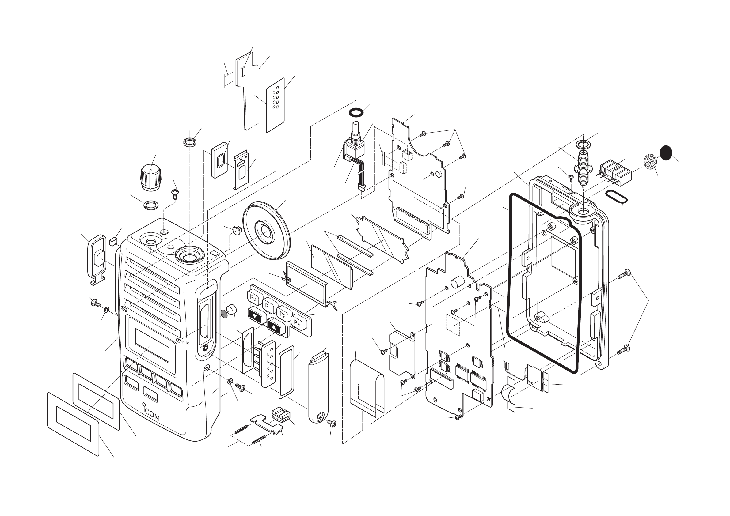
UNIT ABBREVIATIONS:
F=FRONT UNIT
M=MAIN UNIT
V=VR UNIT
CO=CONNECT
UNIT
C=CHASSIS PARTS
)
)
MP406(F
MP10(C
MP429(F
)
MP421(F
MP15(C
J1(CO)
CONNECT UNIT
W404(F)
MP419(F
<A>
MP9(C
)
)
)
MP407(F
MP409(F
)
)
MP406(F
)
SP401(F
)
)
EP402(F
DS401(F
VR UNIT
)
W601(V)
MP410(F
)
MP6(C
R601(V
W404
(F)
<A>
)
)
)
FRONT Unit
MP424(F
MP424(F
)
)
MP3(C
MAIN Unit
MP1(C
)
MP8(C
)
J1(C
)
MP13(C
)
)
MP2(C
MP7(C
)
MP4(C
MP5(C
)
)
)
MP15(C)
MP11(C)
MP401(F)
MP412(F
(
MP408
MP423(F
MP426(F
MP418(F
)
)
MP15(C
MP11(C
)
)
)
MP415(F
)
F
MP701(CO
)
MP414(F
)
)
MP417(F
MP413(F
)
MP404(F
MP2(A
)
)
MP3(A
)
)
)
MP12(C
W401(F
MP12(C
MP4(M
)
)
MP12(C
)
)
)
MP3(M
)
MP18(C
)*
MF1(M
)*
*: Except [A], [D], [G], [J]
)
MP12(C
MP12(C
)
MP14(C
)
MP411(F)
7 - 2
Page 35

SECTION 8 BOARD LAYOUTS
BAT+
• FRONT UNIT
(TOP VIEW)
C494
-
+
ECM(MC1)
R541
R402
C401
C496
1
R479
IC403
C499
C493
C481
R408
IC407
IC406
C497
R513
C500
R410
C495
C489
C406
R405
R511
R401
C404
R406
C405
C498
C482
C450
R433
R429
R426
R535
R480
R430
C423
C449
R428
C421
R432
C425
R427
3
R407
C474
R512
C407
R508
C505C506
R507
R526
R506
R527
C507
IC411
R528 R529
C492
C464
R418
V0 V5 V10 V15 V20 V25 V30 V35 V40 V45 V50 V55 V60 V65 V70
H0H5H10H15H20H25H30H35H40H45
D407
IC409
R530
R496
C508
R497
R486
R485
R411
C402
Q412
D403
R484
R483
C463
R417
C435
C444
R469
R470
C447
R524
R523
Q406
R478
R468
R525
C488
C443
C510
R476R477
C446
C448
R467
C442
IC401
TONE
GND
MIC
C441
CDCS
R466
C420
C419
SIGNAL
SO
SCK
IC405
Q408
R509
MSCK
MDIO
R521
R522
R518
VCC
AFO
AFO
OPTV
GND
GND
RES
J403
J403
CLO
C408
C409
R420
R421
R422
C476
R500
R501
Q411
C479
R412
R413
C465
J401
J401
MTCK
EXSM
EXOE
MTDT
PLST
NOIS
INT
SS
B6802B
R519R520
CLI
MIC
PTT
C410
C467
SDEC
R423
R464
C403
CDEC
R517
C411
R463
C502
KR1
PWON VRON VRIN PWON
C503
C485
C486
R515
C475
C477
C478
C431
R437
R465
C445
R462
R461
R488
R489
R473
R474
R487
C462
R416
IC408
TEMP
UNLK
RSSI
LVIN
C487
R490
R472
MDIR
J402
Q402
R438
C430
R471
R403
C415
D402
MRDF
DAST
D406
R440
R475
C501
RAC
R409
R404
PWON
C429
Q401
R532R533
R439
R516
R534
R482
D401
R495
C412
C466
R414
GND
GND
C428
C491
R441
D404
C414
R493
S5V
R494
C413
C473
CPU5
C432
C483
R502
N/C
R415
C461
R491 R492
Q409
C418
C416 C417
R503
VCC
VCC
C504
C427
Q414
IC410
C490
C468
Q407
R456
R455
X401
4
S401
2
• VR UNIT
(TOP VIEW)
R601
V0 V5 V10
H0H5
• CONNECT UNIT
(TOP VIEW)
B6804
PTT
MIC
CLO
CLI
RES
GND
GND
J1
J1
OPTV
AFO
AFO
VCC
D702
R701
D704
D703
D705
EP705
EP704
C704
EP703
C702
EP702
C701
V0 V5 V10 V15 V20 V25 V30 V35 V40
H0H5H10
D701
AFO
VCC
OPTV
MICE
RESET
RXD
TXD
MIC
PTT
EP701
BAT–
• MAIN UNIT
(TOP VIEW)
MP4
S5V
C241
VCC
B6805BVHF
C200
+5V
C306
R194
IC12
C281
C299
C300
VCC
VCC
N/C
CPU5
S5V
GND
GND
PWON
RAC
C298
C301
T5V
C109
R76
C105
R5V
R111
IC17
C303
R192R193
DAST
MRDF
MDIR
MOTOR
C207
UNLK
C271
TEMP
J2
S1
C237
+
IC9
C307
EP9
F1
C296
R167
C293
R168
C297
–
H75H80
C236
Q26
C295
C230
H70
EP2
C85
L18
C81
C86 C87
Q8
R213
R171R172
C30
R173
R174
C23
R148
IC5
R151
C170
C243
IC6
X1
D6D7
C17
L31
C19
C18
C25
D8
R11
C20
C27
R14
C22
R13
C186
D4
R153
C229
C26
C28
C29
R15
C32
C33
R16
C37
R20
C38
D9
C39
R21
C43
C40
R23
C45
D10
C42
R22
H35H40H45H50H55H60H65
R157
R154
C171
C172
R152
H30
R155
R12
R19
Q2
D23
C218
R150
Q11
C205
L32
C103
C206
C208
R109
C106
R61
L41
R75
C247
C248
C249
C250
C245
C88
C92
R57
R58
C111
R87
C201C202
L42L43
IC16
IC11
R135
C246
R77
C104
Q16
R113
C265
Q7
C78
C89
R59
Q15
C110
C84
C94
C98
R70
L28
C203
C83
R53R54
R10
C91
R55
C77
C100
R71
C107
L21
C139
R88
EP1
R80
L27
R95
C138
D18
R86
LV
C213
R105
R102
R134
C266
R103
R141
R122
C252
C251
R121
C211
C261
EP4
R4
R2
C79
R9
C73
R8
R5
D25
R3
R96
C145
C185
C269
R131
R129
R130
C76
R132
IC2
C219
C267
Q18
R89
R187
C150
R7
R119
R6
C80
C141
R100
R101
C143
C147
C146
R188
C228
R104
R110
R189
R120
Q1
R175
C180
R147
R196
C262
R207
C253
C220
C326C327
R205R206
C254
R123
R124
R36
C75
C263
IC10
EP5
R126
C256
R136
J1
J1
RSSI
LVIN
KR1
CDEC
SDEC
NOIS
MTCK
MTDT
EXOE
EXSM
INT
PLSTSSMSCK
MDIO
SCKSOSIGNAL
CDCS
TONE
GND
MIC
GND
J1
8 - 1
H0H5H10H15H20H25
V0 V5 V10 V15 V20 V25 V30 V35 V40
Page 36

• MAIN UNIT
P0
P1
P2
P3
(BOTTOM VIEW)
C3
L1
C2
L2
C4
C5
C6
C14
L5
D5
C16
L7
L8
L9
MP5
C41
L11
R25
C44
C55
FI1
D26
C329
C67
C59
C60
R33
R34
R35
C58
R48
Q4
C61
R39
R40
R51
L6
C31
C35
C51
R32
R38
C188
C167
• FRONT UNIT
(BOTTOM VIEW)
• VR UNIT
(BOTTOM VIEW)
EP8
R165
C292
L20
Q23
C1
C302
L4
C12
C10
C8
L3
C7
D2
R18
C36
L15
C184
R17
C9
R1
C308
D1
C101
R52
C24
C49
C323
C15
C182
R24
R50
C183
C324
L14
L12
R28
Q3
C52
R30
C54
C53
C56
C63
C65
IC1
R27
C322
R26
C321
C48
C50
R29
L13
C57
R31
C240
R92
C132
C227
C166
C164
C163
L33
C62
R43
C255
C66
R125
C68
R42
R46
R45
C70
R44
C69
C71
C291
C72
C74
R91
C135
R90
Q19
C13
C11
C168
C169
C162
C153
C152
L16
C154
C165
L35
R69
D16
R117
R118
R115
R116
L17
C82
99C79C
R68
D14 D15
Q10
Q13
C119C120
D17
C195
C192
C124
C193
L38
D21
C149
IC4
FI2
FI2
R181
R182
C221
R178
C223
MP1
R67
R72
C122
R83
C121
R82
R84
C123
L24
C194
L25
C129
C133C134
R97
C161
C264
R179
R186
Q24
R166
C234
C239
Q25
C233
C235
C95
L19
C115
R93
C140
D20
C260
Q9
Q12
Q14
L37
D22
D24
R94
EP6
R108
C96
R62
C90
C113
C190
C191
C127
L26
C151
C155
C156
C157
C287
R63
C93
R65
C102
L22
R78
C118
C117
C116
D19
L39
C209
R85
R79
R81
C114
C126
R191
X2
R190
C159
C108
C231
EP3
C238
R162
C242
C158
C319
Q21
R161
Q17
C318
C313
Q22
C137
R199
R202
R201
R98
R212
D12
R198
R163
R164
Q29
IC7
C148
Q31
Q30
C316
IC19
R208
C305
C317
C315
R203
C232
C328
C314
C320
R210 R211
R169
R170
X4
IC18
C325
R197
R204
C311
C259
C199
C222
R183
Q6
R180
R184
R185
C225
C294
R127
R128
C310
C258
C309
C312
B6803
V0V5V10
H0 H5
• CONNECT UNIT
(BOTTOM VIEW)
MP701
V25V30V35V40
AFO
VCC
OPTV
MICE
RESET
RXD
TXD
MIC
PTT
V0V5V10V15V20
H0 H5 H10
R457
DS406
R458
DS405
C426
R434
C437
DS403
R445
Q413
R446
R539
C513
Q415
R537R538
C512
MC401
DS404
DS402
V0V5V10V15V20V25V30V35V40V45V50V55V60V65V70
H0 H5 H10 H15 H20 H25 H30 H35 H40 H45
H0 H5 H10 H15 H20 H25 H30 H35 H40 H45 H50 H55 H60 H65 H70 H75 H80
V0V5V10V15V20V25V30V35V40
S-14406XH-P2
Printed in Japan
© 2007 Icom Inc.
8 - 2
Page 37

SECTION 9 BLOCK DIAGRAM
BAL
REF
IC16
NJM12904
BUFF
Q19
KTC4075
X3
BPF
D/A
IC6
M62363FP
45.9MHz
15.3MHz
X2
CR-783
TCXO
PLL
IC
SQIN
DET
MOD
TEMP
LVIN
IC4
MB15A02
LVA,T1,T2
DET
CTCSS/DTCS
MOD
TONE
CTCSS/DTCS DEC
DET
+5V
R190
IC11
TC4W53FU
FM/PM
SW
IC5
NJM12904
LPF
Q6
XP4601
IC403
NJM12902
LPF
S5V
RIPPLE
LV
IC17
TC4S66F
RSSI
Q17
KTC4075
FIL
FAST
SW
LPF
LIMIT
AMP
BPF
NOIS
D22
HVC375B
LV
ADJ
D21
HVC375B
LV
ADJ
IC16
NJM12904
BUFF
IC5
NJM12904
BUFF
HPF
MSK
DE-Modu
lator
LPFLPF
19.6608MHz CSFT
CR-764
X401
SDEC
LVA
SCRM
D404
M A2S077
RX VCO
TX VCO
FM
MOD
BLER
X4
CR-765
3.6864MHz
SHIFT
SW
Q14 2SC4226
D19,20:HVC376B
Q13
2SC4226
D16,17:HVC376B
D18
1SV239
EXPANDER
COM-
PRESSOR
IC10
AK2346
IC7
EW-460
BATT
SELECT
Q18
2SK880
BUFF
LOOP
FIL
LPF
IF IC
IC1:TA31136FN
X1
CDBKB450KCAY24
SENC0-3 CLI CLO
FI2
CERAMIC
BPF
CFWKA450KFFA
450KHz
AMP
LPF
MSK
Modu
lator
CDEC
Q15:XP1214
Q16:KRC404E
VCO
SW
Q12
2SC5107
BUFF
Q11
2SC5107
BUFF
Q4
2SC4215
IF
AMP
AMP
AMP
IC12
CD4094
EXPAN
IC410
CD4094
EXPAN
DER
DER
R5V
Q10
2SC5107
BUFF
FI1
FL-335
XTAL
BPF
46.35MHz
T5C
R5C
S5C
VCC
VOXV
MAIN UNIT
D14,D15
MA2S077
TX/RX
SW
LPF
182.35MHz-220.35MHz
Q3
3SK324
MIXER
IC18
ISD4002-120
PLAY/
REC
Q 23:KTA1664Y
Q 24:KTC811U
Q25:KRA304E
S5
REG
+5
REG
IC9
NJM2870
D10
HVC350B
BPF
IC19
S-812C33AMC
Q21
KTA2015
Q22
KTA2015
Q9
2SC5110
PRE
DRIVE
Q1
2SK1829
RSSI
D9
HVC350B
BPF
T2 T1
SIGNAL
+5V
+3.3
REG
T5V
T5
REG
R5V
R5
REG
S5V
+5V
GATE
CTRL
RF
AMP
Q2
3SK293
IC406
TC7W66FK
AF
MUTE
TON E
BEEP
VOX
DET
IC411:TC75S51FU
DS402_403
SML-310MT
DS404_405
SML-A12MT
G
R
DS406
CL-165HR
Q8
RD01MUS1
DRIVE
AMP
D4
HVC375B
BPF
IC403
NJM12902
LPF
Q415
2SC4213B
MAX
MUTE
AMP
IC407
NJM12904
LED
CTRL
Q407:KRA304E
Q409:XP4111
Q7
RD07MVS2
PWR
AMP
D8
HVC375B
BPF
AF VOL
IC2
TA75S01F
APC
AMP
D1
RB706F
PWR
DET
T2
VCC
IC405
TDA8547TS
AF
AMP
PWR
CTRL
Q 401:RSQ035P03TR
Q402:KTC811U
IC406
TC7W66FK
MIC
MUTE
D401:MA2S111
D402:MA2S111
PTT
DET
D2:1SV307
D5:1SV307
D25
MA2S111
POWER
IC405
TDA8547TS
AF
AMP
ANT
SW
MUTE
SW
TMUT
Q26
RSQ035P03
SW
SPON
SP/ESP
SW
AFO
MIC
PTT
VCC
RESET
OPTV
LPF
Q30:KTC4075
Q31:KTA1664Y
VIB
REG
VIB
F1
1 2
Q406:KRC404E
Q414:KRC404E
MC1
PTT
CONNECTOR
136-174MHz
MF1
BT1
BATTERY_1
SP1
CDCS
IC40 3
NJM12902
LPF
Q408
KRC404E
FIL
SW
DUSE
9 - 1
CPU
IC401
RESCENC0-2
CPU5
IC408
BD5242G
RESET
IC409
HN58X24256
EEPROM
LCD
FRONT UNIT
Explanatory notes
CONTROL LINE
COMMON LINE
TX LINE
RX LINE
DATA LINE
Page 38

SECTION 10 VOLTAGE DIAGRAM
EP701
AFO
EP702
VCC
EP703
MICE
2403
MMZ1005S601CT x3
MP701
1
2
3
4
5
6
7
8
9
OPTV
RESET
RXD
TXD
AVR-M1005C080MT
AVR-M1005C080MT
EP704
MIC
MMZ1005S601CT
EP705
PTT
MMZ1005S601CT
R701
1k
CONNECT UNIT
AVR-M1005C080MT
AVR-M1005C080MT
C701
D701
D702
AVR-M1005C080MT
AFO
VCC
0.001
0.001
C702
D703
D704
MIC
C704
0.001
D705
R601
TP76N97N
VR UNIT
OPTV
RES
CLI
CLO
J1
11FH-SM1-TB
11
13
10
9
8
7
6
5
4
3
2
12
1
W601
OPC-1260
4
3
2
1
AF Min Level ON :0.00V
AF Min Level OFF:4.91V
SP401
036D0801B
11
10
9
8
7
6
5
4
3
2
12 13
1
11FH-SM1-TB
J403
J402
SM04B-SRSS-TB
56
1
2
3
4
W401
OPC-1210A
100
R445
Q413
RSR025N03
W402
ERDS2T0
PRG21BC4R7MM1RA
R515
VCC
AFO
OPTV
GND
RES
CLI
CLO
MIC
PTT
R446
100K
0.001
C485
C486
C500
S401
SKHLLFA010
POWER OFF:7.07V
POWER ON :0.00V
MC401
EM6027P
R434
470
0.001
C426
33 MSVB2
C496
33 MSVB2
C435
R517
C502
0.1
R518
C503
1
R420
CPU5
COM2
COM1
SEG29
SEG30
SEG31
COM3
COM4
Light ON :4.81V
SML-310M T
Light OFF:0.00V
SML-310M T
DS402
DS403
SML-A12M T
DS405
DS404
DS406
YG
R457
R458
HR
CL-165HR
TX:4.98V
RX:0.00V
C406
0.0027
IC407
C405
1
0.0022
R426
1M
47KR427
C421
R428
0.1
47K
AFON ON EXT SP:7.20V
AFON ON INT SP:4.51V
AFON OFF :0.00V
10 MSVA
10 MSVA
C427
C504
C428
R525
KRC404E
Q414
SEG32
SEG13
SEG14
SEG15
SEG16
SML-A12M T
470
1K
R406
8.2K
R405
15K
R512
100K
0.1
C429
R516
2.2K
0.001
CP1
CP2
CP10S
0.1
MA2S111
0.001
C494
R402
C437
1
R521
12K
100K
R519
10K
R520
10K
R522
10K
150K
CP3
CP10S
CP10S
R403
1K
D401
TX:0.57V
RX:4.84V
Q412
KRA304E
100K
R410
0.001
C495
2.2K
R401
0.001
C404
R541
10K
33K
14
C423
0.001
C401
R430
C425
220P
R432
100K
13
12
IC403
NJM12902V
C513
1
R537
10K
20
19
18
17
16
15
14
13
12
11
AFON ON EXT SP:3.35V
AFON ON INT SP:2.13V
AFON OFF :0.00V
0.001
C475
MA2S111
5
TC7W66FK
4
0.22
10K
100K
R433
R538
VCC1
NC
OUT1IN1IN1+
IN2+
IN2OUT2NC
VCC2
R509
0.001
C476
D402
1K
MA2S111
8
7
6
1
2
3
0.001
C482
33K
TDA8547TS
1K R523
R539
4.7K
10K
R404
100K
IC406
IC405
C477
CP4
CP10S
R409
D403
C497
0.056
C512
1
Q415
2SC4213
GND1
OUT1 +
MODE
SVRR
SELECT
OUT2 +
GND2
47P
NC
NC
NC
C403
C478
MCON
C481
OPTV
CLO
0.001
1
2
3
4
5
6
7
8
9
10
1 SVA
RES
CL I
47P
MD
C479
PTT
R513
0.001
5.6K
0.001
R408
100K
R535
68K
C510
C402
0.001
C498
100P
R511
100K
2
3
NJM12904V
4.7K
R429
100K
R524
100K
Q406
KRC404E
SEG27
SEG28
To LCD
SEG11
SEG12
R455
470
R456
100
RSQ035P03TR
0.001
2.2K
100K
SEG25
SEG26
SEG9
SEG10
TX:0.00V
RX:4.88V
4
5
6
XP4111
R439
R438
SEG22
SEG24
SEG23
SEG8
SEG7
SEG6
Q407
KRA304E
Q409
LEDR
C407
100P
R407
330K
6
5
NJM12904V
BEEP
SIGNAL
456
0.001
C430
SEG19
SEG20
SEG21
SEG5
SEG4
SEG3
3
2
1
R482
100K
IC407
Q401
5
6
123
1K
EXT SP:4.87V
INT SP:0.00V
SEG18
SEG2
LIGT
7
123
SEG17
SEG1
4
R533
10K
R437
C431
LEDT
AFON
SCKSOEXSF
R507
R508
R532
KTC811U
Q40 2
D406
MA2S111
0.01
C487
C490
1
STR
2
D
3
CLK
4
Q1
5
Q2
6
Q3
7
Q4
8
GND9QS
27K
R506
2.2K
C474
270K
0.001
0.001
C488
IC 4 1 0
V+
OE
Q5
Q6
Q7
Q8
Q’S
CD4094BPWR
3.3K
1
0.001
C432
68K
R441
470K
R440
R534
0.001
VCC
100K
11
16
15
14
13
12
11
10
DUSE
C483
4
V+
GND
IC403
NJM12902V
MCON
CSFT
0.001
EXOE
SPON
C489
C444
Q408
KRC404E
BPMAX
0.001
0.1
R470
1
2
3
4
8
GND
4
0.018
R526
V+
0.001
C491
IC409
A0
VCC
A1
A2
VSS5SDA
HN58X24256FPIE
NJM12904V
IC407
R469
4.7K
47K
TX DTCS ON :4.98V
TX DTCS OFF:0.00V
C505
C506
0.018
15K
R527
SCL
WP
330K
SEG23
SEG22
SEG21
SEG20
SEG19
SEG18
SEG17
SEG16
SEG15
SEG14
SEG13
SEG12
SEG11
SEG10
SEG9
SEG8
SEG7
SEG6
SEG5
SEG4
SEG3
SEG2
SEG1
0.001
C492
8
7
6
IC403
1
NJM12902V
470P
C507
R528
27K
0.1
C408
C493
0.1
10K
10K
R497
R496
2
3
820P
C443
R529
10K
5
3
1
IC411
2
TC75S51FU
2.7K
0.1
C442
R468
10
11
12
13
14
15
16
17
18
19
20
21
22
23
24
25
47K
4
1
2
3
4
5
6
7
8
9
0.1
SEG31
SEG30
SEG29
SEG28
SEG27
SEG26
SEG25
PL7/SEG24
PL6/SEG23
PL5/SEG22
PL4/SEG21
CVCC
PL3/SEG20
VSS
PL2/SEG19
PL1/SEG18
PL0/SEG17
PK7/SEG16
PK6/SEG15
PK5/SEG14
PK4/SEG13
PK3/SEG12
PK2/SEG11
PK1/SEG10
PK0/SEG9
R467
47K
D407
MA2S111
CPU5
R421
100K
C409
R485
100K
C441
C508
R486
0.015
C499
470P
1K
R466
0.1
SEG24
100
26
47K
10K
47P
VOXV
R530
R422
100K
C410
SEG25
SEG26
SEG27
SEG28
SEG32
PJ7/WKP7/SEG8
PJ6/WKP6/SEG7
PJ5/WKP5/SEG6
PJ4/WKP4/SEG5
PJ3/WKP3/SEG4
27
28
29
30
31
MSCKSOPLST
MDIO
SCK
R465
0.0033
C449
IC403
8
NJM12902V
1M
R423
100K
0.1
C411
COM1
COM2
COM3
SEG29
SEG30
SEG31
SEG32
92
SEG4093SEG3994SEG3895SEG3796SEG3697SEG3598SEG3499SEG33
PJ2/WKP2/SEG3
PJ1/WKP1/SEG2
PJ0/WKP0/SEG1
P1035P1136P12/TCLKA37P13/TCLKB38P14/TIOCA1/IRQ0
32
33
34
EXOE
EXSM
EXSF
INT
SS
R480
10
68K
9
47P
C450
DAST
COM4
PH3/COM 489PH2/COM 390PH1/COM 291PH0/COM 1
CENC2
81
82
83
84
85V386V287V188
PH5
PH4/ φ
P35/SCK1/SCL0
PF3/ADTRG/IRQ3
P15/TIOCB1/TCLKC
P16/TIOCA2/IRQ1
P17/TIOCB242AVSS43P97/AN944P96/AN845P47/AN746P46/AN647P45/AN548P44/AN449P43/AN350P42/AN2
39
40
41
CDEC
SDEC
NOIS
VOXV
MTCK
MTDT
R479
68K
7
TONE
CDCS
MIC
100K
MRDF
C501
CENC1
CENC0
76
77
78
79
80
P31/RXD0
P33/TSC1
P34/RXD1/SDA0
P32/SCK0/IRQ4
RSSI
LVIN
BATV
0.0022
C447
5
6
IC403
NJM12902V
C473
R502
CLO
CLI
R488
470P
R489
10K
IC401
P30/TXD0
P70/TMRI01/TMCI01
P72/TMO0
P73/TMO1
P75/SCK2
P46/RXD2
P77/TXD2
P40/AN0
P41/AN1
HD64F2268TFV
R484
R483
100K
100K
C445
R477
68K
R478
68K
C448
120P
BATV
100K
R503
0.01
100K
R490
10K
ESTAL
XTAL
STBY
OSC1
OSC2
AVCC
VREF
FW E
VCC
NMI
MD1
PH7
SO
SCK
MDIO
MSCK
SS
PLST
INT
EXSM
EXOE
MTDT
MTCK
NOIS
SDEC
CDEC
LVIN
RSSI
TEMP
UNLK
MDIR
MRDF
DAST
RAC
P71
P74
MD2
VSS
RES
0.001
C446
R464
75
74
73
72
71
70
69
68
67
66
65
64
63
62
61
60
59
58
57
56
55
54
53
52
51
22K
R476
68K
0.001
R487
10 MSVA
R475
C419
10K
4.96V
100K
BPMAX
C420
R461
180K
R462
R463
MDIR
UNLK
OPTV
TEMP
22K
FRONT UNIT
C412
0.1
R495
12K
CR-764
SENC0
SENC1
SENC2
SENC3
PTT
RAC
RES
MD
CSFT
0.1
CENC0
CENC1
56K
CENC2
R471
SENC0
220K
R472
SENC1
100K
R473
SENC2
47K
R474
SENC3
22K
CPU5
KR0
KR1
100K
10
R501
KRC404E
UP
R413
X401
R492
1M
R491
12P
C416
100K
R500
1
2
VDD
3
VSS
Q411
R411
S407
P0 P1
KEY
150K
R415
47P
C461
C467
S406
KEY
27K
47P
C465
CP10S
CP5
CP10S
CP6
KR1
S5V
PWON
VCC
VCC
19.66MHz
1.44Vp-p
C417
IC408
OUT
BD5242 G
100K
R416
47P
MA2S077
C414
15P
R493
6P
5
CD
4
NC
R412
S402
P2
KEY
150K
R417
47P
C462
S405
DN
KEY
27K
R414
C466
J401
IMSA-9681S-36A-TB
GND
GND
GND
12K
47P
D404
C415
36
35
34
33
32
31
30
29
28
27
26
25
24
23
22
21
20
19
18
17
16
15
14
13
12
11
10
9
8
7
6
5
4
3
2
1
100K
S403
KEY
470K
C468
0.01
C463
R494
C413
0.1
12K
0.1
C418
S404
P3
KEY
470K
R418
47P
47P
C464
47P
38
37
10 - 1
*; Refer to “PARTS LIST.”
Page 39
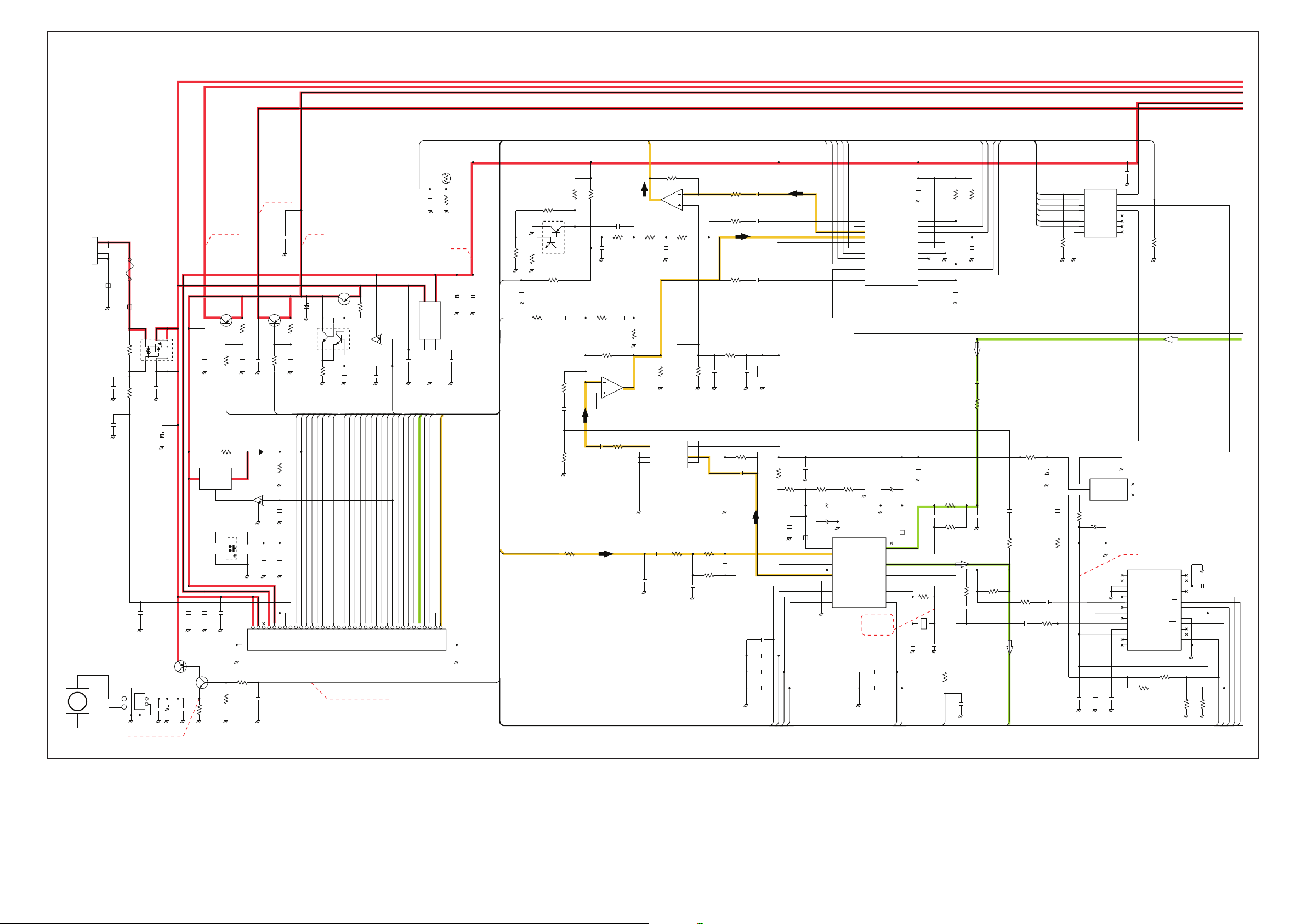
MAIN UNIT (Left side)
MP2(CHASSIS)
4
3
2
1
2403
M
Vibration Motor
(MF1)
MPZ2012S331A
EP8
C296
C297
ERBFE3R00U
R167
0.001
R168
0.001
12
EP9
Vibration ON :3.59V
Vibration OFF:0.00V
F1
M PZ1608S101A
RSQ035P03TR
Q26
4
270K
3
C295
100K
0.001
C301
*J2
2
1
3 4
5
2
10
*C317
0.001
*Q31
C236
6
1
*C316
C298
*Q30
*C315
C241
IC7
EW-460
1
I2O
0.001
C299
*R203
T5V
TX:5.01V
RX:0.00V
+5V
VCC
S5V
KTA2015
Q21
R162
0.001
R169
100K
G
3
EVQP7M01K
0.001
C300
*R202
T5C
0.001
4.7K
S1
*R201
R161
C231
KRC404E
10K
0.01
C242
D1 2
MA2S111
Q29
36
38
*C318
TX:0.00V
RX:4.97V
KTA2015
Q22
0.001
C293
34
35
R164
R5C
R170
0.001
33
C305
C294
32
C230
4.7K
31
R163
C232
470K
47P
0.001
30
0.001
RAC
29
22 MSVB2
10K
0.01
DAST
MRDF
27
28
5.02V
MDIR
26
KTA1664
Q23
C233
4
5
6
123
2.2K
R166
C234
RSSI
LVIN
UNLK
TEMP
20
21
22
23
24
25
Vibration ON :4.98V
Vibration OFF:0.00V
CDEC
19
SDEC
R165
Q24
KTC811U
470P
NOIS
MTCK
17
18
10K
MTDT
15
16
KRA304E
C235
EXOE
EXSM
13
14
Q25
INT
C307
0.01
S5C
SS
SCK
PLST
MDIO
MSCK
8
9
10
11
12
IMSA-9681S-36A-TB
VCC
A
T5V
B
S5V
C
+5V
D
R5V
E
T1
R196
C243
0.022
0.1
R125
C254
R128
0.1
470
0.1
REF
C255
47K
0.0012
C256
LVA
0.0022
R126
330K
T2
IC12
STR
D
CLK
Q1
Q2
Q3
Q4
GND9QS
CD4094BPWR
*IC19
GBD
VIN
VOUT4NC
*C312
V+
OE
Q5
Q6
Q7
Q8
Q’S
*C311
16
15
14
13
12
11
10
NC
15
16
17
18
19
20
21
22
23
24
25
26
27
28
*C326
*R205
SIGNAL
*R127
*C310
*R212
EXSM
SO
SCK
R5C
T5C
VIB
S5C
*C309
*R197
*C328
*C325
*R204
100K
R193
1
2
3
4
5
6
7
8
*R208
*C314
1
2
3
*C319
*C320
C281
3.33V
0.1
PMFM
5
NC
NC
VSSA
VSSA
NC
AUDOUT
NC
AMCAP
NC
ANAIN ANAIN+
VCCA
NC
NC
*R19 9
R192
EXOE
*R198
100K
VSSD
MISO
MOSI
SCLK
VCCD
XCLK
INT
RAC
VSSA
*IC18
SQLO
F
SQLI
G
TMUT
H
NC
14
NC
*C313
13
12
11
10
SS
9
8
7
6
5
NC
4
NC
3
2
1
*R210
*R211
SS
INT
RAC
SCK
SO
I
SO
SCK
0.001
C267
EP4
0.01
2.2K
R131
C261
1 ESVP
C262
1 ESVP
ACZ1005Y
10
11
12
BAL
1
2
3
4
5
6
7
8
9
DAS T
CDCS
IC6
1
VIN1
2
VOUT1
3
VOUT2
4
VIN2
5
VDD
6
LD
7
CLK
8
DI
9
VIN3
10
VOUT3
11
VOUT4
12
VIN4
M62363FP
47K
R132
IC10
AGNDIN
AGND
TXIN
RXLPFO
TXINO
LIMLV
EXTLMI N
MOD
VSS
TCLK
TDATA
DI/O
RDF/FC13SCLK
AK2346P
RXAFIN
EXPOUT
3.68MH
1.48Vp-p
C246
47P
C245
47P
TEST
RXIN
RXINO
RXAF
VDD
XOUT
XIN
DIR
22 MSVA
C264
C263
0.001
24
23
22
21
20
19
18
17
16
15
14
VOUT8
VOUT7
RESET
VDAREF
VOUT6
VOUT5
EP5
MSCK
MDIR
VIN8
VIN7
GND
DO
VIN6
VIN5
ACZ1005Y
22P
C227
C306
R135
1M
X4
CR-765
C259
24
23
22
21
20
19
18
17
16
15
14
13
0.01
0.001
180P
C253
22P
+5V
470
R120
0.1
C229
+5V
33K
R124
R123
82K
33K
C258
C260
1K
R136
C220
SDEC
TEMP
ERTJ0EP473J
R190
TEMP
C225
68K
R179
0.001
R152
560K
Q6
R186
100K
3
2
1
1.2K
R180
10K
100K
R191
0.1
C287
4.98V
R178
CDEC
4
5
VIN
IC9
CTRL2GND3NB
1
0.1
SO
CDCS
TONE
SIGNAL
4
5
6
7
C238
0.1
C239
4.7 MSVA
VOUT
NJM2870
0.01
C237
MIC
J1
1
2
3
37
TONE
MIC
VIB
C172
0.001
*R207
*R206
*C327
R194
10K
R185
4
5
6
XP4601
3.3K
R184
15K
R183
R153
150K
150K
R154
2
3
NJM12904V
C170
0.1
SIGNAL
C223
0.01
C222
C171
4.7
IC5
MOD
R189
220K
IC5
6
7
5
NJM12904V
0.1
R182
22K
C221
R157
IC11
COM
INH
VEE
GND5A
TC7W53FK
0.1
C271
0.1
R181
22K
0.039
10K
R141
68K
R148
C180
8
VCC
7
CH0
6
CH1
R121
33K
12K
R122
390K
C252
0.0015
22K
10K
R155
1
R151
1
2
68K
3
4
C303
0.1
R147
100K
C265
C251
10K
R119
R188
220K
R150
NJM12904V
R134
33K
C266
330P
0.001
47P
0
C240
1
C219
0.001
C228
C218
4.7
GND
0.001
IC5
C250
47P
C249
47P
C248
47P
C247
47P
8
V+
4
47K
R129
2.2K
R130
C269
MTCK
MTDT
MDIO
MRDF
*; Refer to “PARTS LIST.”
10 - 2
Page 40

MAIN UNIT (Right side)
C107
C321
C205
C41
12P
68K
0.001
R71
2SC5107
22P
47P
Q10
C322
L12
68N
4P
100K
0.001
VCC
T5V
R68
C108
0.01
R70
100
C99
0.001
3.86V
0.1U
L21
MA2S077
C100
10P
D14
MA2S077
D15
1K
R69
L14
7P
C49
15N
12P
C323
TX:0.00V
RX:1.50V
HVC350B
C40
2P
D10
C44
56N
L11
C45
R23
0.001
C43
R67
15P
C183
C324
150K
0.001
10K
100
TX:1.13V
RX:0.00V
C93
R65
7P
9P
R21
1.5K
R63
C95
R50
C18 2
R24
HVC350B
220K
10K
R61
TX:0.00V
10K
0.001
1K
C39
R22
470
0.001
D9
0.001
10
0.001
TX:0.00V
RX:4.68V
3P
C42
TX:4.75V
RX:0.00V
C106
47P
47N
L19
C92
22P
Q9
2SC5110
C90
R62
100
C94
1
C35
C36
3SK293
C38
R20
0.001
0.001
C96
C97
R59
4.7K
R58
C91
47P
R17
56N
0.001
L9
C37
0.01
C32
820
0.00 1
RF AMP
C292
47P
RD01MUS
47
Q2
C33
47P
EXCCL3225U
L20
0.001
C85
0.001
Q8
1
R57
68
C89
0.01
33K
0.001
10 MSVA
TX:2.26V
RX:0.00V
4.7
C184
0.001
R19
10
R12
R16
270
MMZ1608Y102BT
EP2
C81
82P
22N
L18
C86
C87
27P
C88
R55
0.001
C98
C73
R172
R18
22K
C186
0.1
C31
0.1
100K
C30
0.1
R213
2.5P
C29
R15
L8
120K
TX:0.00V
RX:2.69V
TX:0.00V
RX:1.48V
1
4.7K
0.001
TX:0.00V
RX:1.46V
100K
68N
RD07MVS2
R53
100K
C77
R10
R171
C28
C82
Q7
22
R54
470P
0.001
R9
100
1.5K
Q1
2SK182 9
R173
82K
HVC375B
3.5P
0.001
10
C76
5.6K
100P
C26
L17
2681
C84
C83
R3
0.1
TA75S01F
R174
470K
R175
0.1
18.3N
L16
8.6N
MP 1
4
220K
C23
D4
R13
C27
0.001
AGC
C22
1P
100K
D23
R11
0.001
C30 2
51P
C13
C79
R8
220K
5
2
MA2S111
100K
L4
5.8N
62P
0.1
IC2
3
1
HVC375B
C20
R14
10K
C12
1P
120K
D8
100P
C10
0.001
18P
M A2S111
TX:2.53V
RX:0.00V
R7
C74
L7
0.001
150
R52
0.001
C291
TX:1.69V
RX:0.00V
J1(CHASSIS)
0.001
C101
L15
4.7U
C7
0.00 1
18P
TX:2.05V
RX:2.14V
0.001
0.001
TMUT
D6
D7
MA2S728
MP 5
D2
1SV307
TX:0.00V
RX:4.84V
L6
27N
12P
C17
L3
45.3N
2.7K
R1
C11
C308
D1
D25
APC
R5
C80
0.1
0.001
C25
6P
68N
C24
C8
C9
15P
0.5P
RB706F
R2
4.7K
C15
0.001
10K
R6
C78
68K
10K
R4
C72
0.001
C19
5P
C18
MA2S077
0.1U
L31
O G-503040
0.001
C16
LPF
C6
27.2N
L1
L2
24N
C2
C4
8P
C5
22P
11P
22P
1SV307
C3
L5
45.3N
D5
82K
R51
9P
22P
C1
C14
11P
VCC
A
T5V
B
S5V
C
+5V
D
R5V
E
47K
R102
C211
BAL
R104
REF
220K
LVIN
S5V
UNLK
SCK
SO
PLST
SQLO
F
SQLI
G
TMUT
H
C154
MO D
+5V
D AST
LVA
R5V
2
4.7
3
330K
R105
0.1
C213
R94
150K
0.1
C151
R117
4.7K
R118
4.7K
47P
47P
47P
C152
C153
R115
R116
C161
10P
KTC4075
*3 MULTI
R103
470K
NJM12904V
ACZ1005Y
270P
C155
D24
M A2S111
1.2K
680K
Q19
IC16
0.1
L35
EP6
10
11
12
13
14
15
16
1
9
C185
0.22U
+5V
REF OSC
X2
1
VCON
2
GND3OUT
CR-783
0.1
C140
R93
1K
MB15A02PFV1
CLOCK
DATA
LE
FC
NC
FOUT
P
B
TX:0.00V
RX:3.10V
0.01
C165
C163
4P
56P
C162
OSCOUT
OSCIN
IC4
C164
FIN
GND
VCC
7P
PLL
LD
DO
VP
C159
L33
8
7
6
5
4
3
2
1
0.001
VCC
C157
0.82U
S5V
ACZ1005Y
EP3
0.1
C158
4
10K
10P
R108
C166
3P
CFWKA450KFFA
C169
0.1
C156
FI2
10 MSVA
4P
0.1
10 MSVA
C188
2.2K
C148
L28
3.3U
L27
3.3U
C190
C195
C75
Q17
KTC4075
5P
C191
L26
C127
47P
D2 0
L37
HVC376B
L39
33N
68N
10U
4P
HVC376 B
D1 9
RX VCO
33P
C126
33P
C134
D22
HVC375B
3.9K
L42
R85
C114
C115
3.3U
TX VCO
C203
100
0.01
MA74 2
C59
TX:0.00V
RX:4.63V
150
L43
3.3U
0.001
R33
22P
D21
3.9K
R84
C123
68P
C133
HVC375B
0.001
82N
220P
L25
5P
3P
C194
3P
R38
100K
C61
47P
C63
D17
C192
HVC376B
C193
D1 6
L38
HVC376B
68N
CDBKB450KCAY24
R36
1.5K
X1
100P
C62
82P
2SC4215
C65
0.001
C124
10U
L24
R5V
680
R48
Q4
TX:0.00V
RX:4.78V
IF AMP
1P
C129
D18
R86
1SV239
120K
R35
C60
100K
R34
C58
0.00 1
0.001
C329
D26
1.8K
R81
0
33P
33P
4
2
C139
0.1
R79
Q14
2SC4226
4.7
C121
18P
C122
33P
TX:0.00V
RX:4.88V
GND
OU T3GND
470P
C119
1.8K
R83
R82
2SC4226
C56
Q13
C110
0.001
56
IN
FL-335
27P
EP1
ACZ1005Y
C116
0.75P
C120
470P
TX:2.40V
RX:0.00V
10
0.01
C53
FI1
1
C118
C104
R88
560
R31
C117
0.01
C113
0.5P
R87
C54
C55
3.83V
0.001
2SC5107
0.001
470P
100K
Q12
TX:0.00V
RX:2.40V
470
Q15
5
L13
R32
100
4P
TX:0.00V
RX:0.47V
R78
100
L22
XP1214
0.82U
C52
C51
0.00 1
3SK32
R77
0.1U
C109
R76
4.04V
100
0.001
C105
R75
220K
0.001
0.1U
L41
Q11
10K
Q16
KRC404E
R27
150K
100K
TX:0.00V
RX:1.96V
0.001
C48
0.001
R5V
R26
4.7
R72
C111
68K
R25
0.01
C102
7P
3P
C103
2SC5107
R80
1
2
34
C57
0.001
1K
10P
R30
R28
Q3
4
68
R29
C50
MIX
R98
1K
C135
R101
0.001
CP1
C143
CP06S
0.001
Q18
2SK880
10K
0.001
R100
C141
0.001
R97
560
C149
R96
0.47 SV A
C147
3.3 MSVA
10P
C207
0.001
C209
L32
33N
56
R109
C208
6
5
NJM12904V
0.1
C167
IO
C168
0.1
C71
IC16
12P
0.1
100P
R46
R39
C206
47P
C200
7
47
R40
390K
R44
C69
2.2K
1.5K
C70
12P
10K
1.5K
4
100P
150K
R89
5.6K
R95
R187
5
IC17
TC4S66F
123
R111
100K
TX:0.00V
RX:4.78V
IC1
1
OSCIN
2
OSCOUT
3
M IXOUT
4
VCC
5
IFIN
6
DEC
7
FILOUT
8
FILIN
TA31136FNG
TX:0.00V
RX:1.24V
R45
R92
R91
39K
R110
IF IC
R42
47K
100K
C132
33K
0.1 SVA
C150
1
33K
C199
C201
100P
C68
C146
C145
0.1
C138
0.001
R113
4.7K
1
MIXIN
N-RE C
N-DE T
IF OU T
AFOUT
47P
470P
GND
RSSI
QUAD
R90
8
GND
4
C67
C66
C137
V+
R43
0.01
220K
IC16
NJM12904V
C202
0.001
16
15
14
13
12
11
10
9
470
0.001
0.001
NOIS
I
RSSI
T2
RSSI
T1
T2
*; Refer to “PARTS LIST.”
10 - 3
Page 41

1-1-32, Kamiminami, Hirano-ku, Osaka 547-0003, Japan
Phone : +81 (06) 6793 5302
Fax : +81 (06) 6793 0013
URL : http://www.icom.co.jp/world/index.html
<Corporate Headquarters>
2380 116th Avenue N.E., Bellevue, WA 98004, U.S.A.
Phone : +1 (425) 454-8155 Fax : +1 (425) 454-1509
URL : http://www.icomamerica.com
E-mail : sales@icomamerica.com
<Customer Service>
Phone : +1 (425) 454-7619
Glenwood Centre #150-6165
Highway 17 Delta, B.C., V4K 5B8, Canada
Phone : +1 (604) 952-4266 Fax : +1 (604) 952-0090
URL : http://www.icomcanada.com
E-mail : info@icomcanada.com
Unit 1 / 103 Garden Road, Clayton VIC 3168 Australia
Phone : +61 (03) 9549-7500 Fax : +61 (03) 9549-7505
URL : http://www.icom.net.au
E-mail : sales@icom.net.au
146A Harris Road, East Tamaki,
Auckland, New Zealand
Phone : +64 (09) 274 4062 Fax : +64 (09) 274 4708
URL : http://www.icom.co.nz
E-mail : inquiries@icom.co.nz
10C07, Long silver Mansion, No.88, Yong Ding
Road, Haidian District, Beijing, 100039, China
Phone : +86 (010) 5889 5391/5392/5393
Fax : +86 (010) 5889 5395
E-mail : bjicom@bjicom.com
URL : http://www.bjicom.com
Communication Equipment
Himmelgeister Str. 100, D-40225 Dusseldorf, Germany
Phone : +49 (0211) 346047 Fax : +49 (0211) 333639
URL : http://www.icomeurope.com
E-mail : info@icomeurope.com
Ctra. Rubi, 88, 08190, Sant Cugat del Valles, Barcelona, SPAIN
Phone : +34 (93) 590 26 70 Fax : +34 (93) 589 04 46
URL : http://www.icomspain.com
E-mail : icom@icomspain.com
Unit 9, Sea St., Herne Bay, Kent, CT6 8LD, U.K.
Phone : +44 (01227) 741741 Fax : +44 (01227) 741742
URL : http://www.icomuk.co.uk
E-mail : info@icomuk.co.uk
Zac de la Plaine
1 Rue Brindejonc des Moulinais BP 5804
31505 Toulouse Cedex, France
Phone : +33 (5) 61 36 03 03 Fax : +33 (5) 61 36 03 00
URL : http://www.icom-france.com
E-mail : icom@icom-france.com
6F No.68, Sec. 1 Cheng-Teh Road, Taipei, Taiwan, R.O.C.
Phone : +886 (02) 2559 1899 Fax : +886 (02) 2559 1874
URL : http://www.asia-icom.com
E-mail : sales@asia-icom.com
Sopot, 3 Maja 54 Poland
Phone : +48 (58) 550 7135 Fax : +48 (58) 551 0484
E-mail : icompolska@icompolska.com.pl
Page 42

1-1-32, Kamiminami, Hirano-ku, Osaka 547-0003, Japan
S-14406XZ-C1
© 2007 Icom Inc.
 Loading...