

Page 1

SERVICE
MANUAL
HF/VHF/UHF ALL MODE TRANSCEIVER
S-14214HZ-C1
Dec. 2005
Page 2

INTRODUCTION
DANGER
This service manual describes the latest service information
for the
IC-7000 HF/VHF/UHF ALL MODE TRANSCEIVER
at the time of publication.
VER.NO. VERSION SYMBOL
#02 Europe EUR
#03 France FRA
#04 Spain ESP
#05 U.S.A. USA
#08 Export EXP
#10 United Kingdom UK
To upgrade quality, all electrical or mechanical parts and internal
circuits are subject to change without notice or obligation.
NEVER connect the transceiver to an AC outlet or to a DC
power supply that uses more than 16 V. Such a connection
could cause a fire or electric hazard.
DO NOT expose the transceiver to rain, snow or any liquids.
DO NOT reverse the polarities of the power supply when
connecting the transceiver.
DO NOT apply an RF signal of more than 20 dBm (100 mW)
to the antenna connector. This could damage the transceiver's front end.
ORDERING PARTS
Be sure to include the following four points when ordering
replacement parts:
1. Make sure the problem is internal before disassembling
the transceiver.
REPAIR NOTES
2. DO NOT open the transceiver until the transceiver is
1. 10-digit Icom parts number
2. Component name and informations
3. Equipment model name and unit name
4. Quantity required
disconnected from its power source.
3. DO NOT force any of the variable components. Turn
them slowly and smoothly.
4. DO NOT short any circuits or electronic parts. An
insulated turning tool MUST be used for all adjustments.
<SAMPLE ORDER>
5. DO NOT keep power ON for a long time when the
transceiver is defective.
5030002820 LCD LTA025A161A IC-7000 Front unit 5 pieces
8810009610 Screw FH M2.6 × 6 ZK IC-7000
To p c ove r
10 pieces
6. DO NOT transmit power into a signal generator or a
sweep generator.
7. ALWAYS connect a 50 dB to 60 dB attenuator between
Addresses are provided on the inside back cover for your
convenience.
the transceiver and a deviation meter or spectrum
analyzer when using such test equipment.
8. READ the instructions of test equipment thoroughly
before connecting equipment to the transceiver.
Icom, Icom Inc. and logo are registered trademarks of Icom Incorporated (Japan) in the United States, the United
Kingdom, Germany, France, Spain, Russia and/or other countries.
Page 3

TABLE OF CONTENTS
SECTION 1 SPECIFICATIONS
SECTION 2 INSIDE VIEWS
SECTION 3 CIRCUIT DESCRIPITON
3 - 1 RECEIVER CIRCUITS . . . . . . . . . . . . . . . . . . . . . . . . . . . . . . . . . . . . . . . . . . . . . . . . . . . . . . . . . . . . . . 3 - 1
3 - 2 TRANSMITTER CIRCUITS . . . . . . . . . . . . . . . . . . . . . . . . . . . . . . . . . . . . . . . . . . . . . . . . . . . . . . . . . . . 3 - 4
3 - 3 DDS CIRCUITS . . . . . . . . . . . . . . . . . . . . . . . . . . . . . . . . . . . . . . . . . . . . . . . . . . . . . . . . . . . . . . . . . . . . 3 - 6
3 - 4 LOGIC CIRCUITS . . . . . . . . . . . . . . . . . . . . . . . . . . . . . . . . . . . . . . . . . . . . . . . . . . . . . . . . . . . . . . . . . . 3 - 8
3 - 5 POWER SUPPLY CIRCUITS. . . . . . . . . . . . . . . . . . . . . . . . . . . . . . . . . . . . . . . . . . . . . . . . . . . . . . . . . . 3 - 8
3 - 6 PORT ALLOCATIONS . . . . . . . . . . . . . . . . . . . . . . . . . . . . . . . . . . . . . . . . . . . . . . . . . . . . . . . . . . . . . . . 3 - 9
SECTION 4 ADJUSTMENT PROCEDURES
4 - 1 PREPARATION . . . . . . . . . . . . . . . . . . . . . . . . . . . . . . . . . . . . . . . . . . . . . . . . . . . . . . . . . . . . . . . . . . . . 4 - 1
4 - 2 DDS ADJUSTMENT . . . . . . . . . . . . . . . . . . . . . . . . . . . . . . . . . . . . . . . . . . . . . . . . . . . . . . . . . . . . . . . . 4 - 3
4 - 3 DISPLAY ADJUSTMENT. . . . . . . . . . . . . . . . . . . . . . . . . . . . . . . . . . . . . . . . . . . . . . . . . . . . . . . . . . . . . 4 - 3
4 - 4 TRANSMITTER ADJUSTMENT . . . . . . . . . . . . . . . . . . . . . . . . . . . . . . . . . . . . . . . . . . . . . . . . . . . . . . . 4 - 3
4 - 5 RECEIVER ADJUSTMENT . . . . . . . . . . . . . . . . . . . . . . . . . . . . . . . . . . . . . . . . . . . . . . . . . . . . . . . . . . 4 - 11
SECTION 5 PARTS LIST
SECTION 6 MECHANICAL PARTS AND DISASSEMBLY
SECTION 7 SEMI-CONDUCTOR INFORMATION
SECTION 8 BOARD LAYOUTS
8 - 1 DISPLAY UNIT. . . . . . . . . . . . . . . . . . . . . . . . . . . . . . . . . . . . . . . . . . . . . . . . . . . . . . . . . . . . . . . . . . . . . 8 - 1
8 - 2 VR UNIT . . . . . . . . . . . . . . . . . . . . . . . . . . . . . . . . . . . . . . . . . . . . . . . . . . . . . . . . . . . . . . . . . . . . . . . . . 8 - 1
8 - 3 MAIN UNIT . . . . . . . . . . . . . . . . . . . . . . . . . . . . . . . . . . . . . . . . . . . . . . . . . . . . . . . . . . . . . . . . . . . . . . . 8 - 3
8 - 4 PA UNIT . . . . . . . . . . . . . . . . . . . . . . . . . . . . . . . . . . . . . . . . . . . . . . . . . . . . . . . . . . . . . . . . . . . . . . . . . . 8 - 5
8 - 5 DDS UNIT . . . . . . . . . . . . . . . . . . . . . . . . . . . . . . . . . . . . . . . . . . . . . . . . . . . . . . . . . . . . . . . . . . . . . . . . 8 - 7
8 - 6 LOGIC UNIT . . . . . . . . . . . . . . . . . . . . . . . . . . . . . . . . . . . . . . . . . . . . . . . . . . . . . . . . . . . . . . . . . . . . . . 8 - 9
8 - 7 CONNECT UNIT . . . . . . . . . . . . . . . . . . . . . . . . . . . . . . . . . . . . . . . . . . . . . . . . . . . . . . . . . . . . . . . . . . 8 - 11
8 - 8 DRIVER UNIT . . . . . . . . . . . . . . . . . . . . . . . . . . . . . . . . . . . . . . . . . . . . . . . . . . . . . . . . . . . . . . . . . . . . 8 - 11
8 - 9 HM-151 . . . . . . . . . . . . . . . . . . . . . . . . . . . . . . . . . . . . . . . . . . . . . . . . . . . . . . . . . . . . . . . . . . . . . . . . . 8 - 11
SECTION 9 WIRING DIAGRAM
SECTION 10 BLOCK DIAGRAM
SECTION 11 CIRCUIT DIAGRAMS
11 - 1 DISPLAY/VR/CONNECT UNITS . . . . . . . . . . . . . . . . . . . . . . . . . . . . . . . . . . . . . . . . . . . . . . . . . . . . . 11 - 1
11 - 2 MAIN UNIT . . . . . . . . . . . . . . . . . . . . . . . . . . . . . . . . . . . . . . . . . . . . . . . . . . . . . . . . . . . . . . . . . . . . . . 11 - 3
11 - 3 LOGIC UNIT . . . . . . . . . . . . . . . . . . . . . . . . . . . . . . . . . . . . . . . . . . . . . . . . . . . . . . . . . . . . . . . . . . . . . 11 - 7
11 - 4 PA/DRIVER UNITS . . . . . . . . . . . . . . . . . . . . . . . . . . . . . . . . . . . . . . . . . . . . . . . . . . . . . . . . . . . . . . . 11 - 10
11 - 5 DDS UNIT . . . . . . . . . . . . . . . . . . . . . . . . . . . . . . . . . . . . . . . . . . . . . . . . . . . . . . . . . . . . . . . . . . . . . . 11 - 13
Page 4
SECTION 1 SPECIFICATIONS
¤ GENERAL
• Frequency coverage :
Receive 0.030 – 199.999999 MHz*
400.000 – 470.000000 MHz*
Transmit 1.800 – 1.999999 MHz*
3.500 – 3.999999 MHz*
5.260 – 5.405000 MHz*
7.000 – 7.300000 MHz*
10.100 – 10.150000 MHz
14.000 – 14.350000 MHz
18.068 – 18.168000 MHz
21.000 – 21.450000 MHz
24.890 – 24.990000 MHz
28.000 – 29.700000 MHz
50.000 – 54.000000 MHz*
144.000 – 148.000000 MHz*
430.000 – 450.000000 MHz*
*1 Some frequency bands are not guaranteed.
*
2
Depending on version.
• Mode : USB, LSB, CW, RTTY (FSK), AM,
FM, WFM (WFM is for receiver only)
• Number of memory ch. : 503 (495 split, 6 scan edges, 2 call)
• Antenna connector : SO-239 × 2
(for HF/50 MHz and 144/430 MHz)/50
• Power supply requirement : 13.8 V DC ±15% (negative ground)
• Frequency stability : Less than ±0.5 ppm
(0˚C to +50˚C ;+32˚F to +122˚F)
• Current drain :
Transmit at 100 W 22 A
Receive standby 1.3 A
max. audio 1.6 A
• Usable temperature range : –10˚C to +60˚C (+14˚F to +140˚F)
• Dimensions : 167(W) × 58(H) × 180(D) mm
9
(proj. not included) 6
⁄16(W) × 29⁄32(H) × 73⁄32(D) inch
• Weight (approx.) : 2.3 kg (5 lb 1 oz)
• CI-V connectors : 2-conductor 3.5 (d) mm (
• Video connector : 2-conductor 3.5 (d) mm (
• ACC connector : 13-pin
• Data connector : 6-pin
1
2
,
*
1
2
,
*
2
2
2
2
2
2
2
Ω
1
⁄8″)
1
⁄8″)
¤ TRANSMITTER
• Output power :
SSB/CW/
RTTY/FM
1.8–50 MHz bands 2–100 W 1–40 W
144 MHz band 2–50 W 2–20 W
430 MHz band 2–35 W 2–14 W
• Modulation system :
SSB Digital PSN modulation
AM Digital Low Power modulation
FM Digital Phase modulation
• Spurious emissions :
below 30 MHz bands Less than –50 dB
above 50 MHz bands Less than –60 dB
• Carrier suppression : More than 50 dB
• Unwanted sideband : More than 50 dB
• Microphone connector : 8-pin modular jack (600 Ω)
• KEY connector : 3-conductor 6.35 (d) mm (
• RTTY connector : 3-conductor 3.5 (d) mm (
AM
1
⁄4″)
1
⁄8″)
¤ RECEIVER
• Receive system :
SSB/CW/AM/FM Triple conversion superheterodyne
WFM Double conversion superheterodyne
• Intermediate frequencies :
1st IF 2nd IF 3rd IF
SSB/CW/AM/
RTTY/FM
WFM 134.732 MHz 10.700 MHz ––
• Receive sensitivity : (pre-amp ON)
0.5–1.8 MHz –– 13 µV –– ––
1.8–28 MHz*
28–29.995 MHz*
50 MHz band 0.12 µV 1.0 µV 0.25 µV ––
76–108 MHz –– –– –– 10 µV
144/430 MHz
bands
Note: SSB, CW and AM modes are measured at 10 dB S/N; FM mode at
12 dB SINAD.
1
*
Except 4–4.5 MHz, 8–9 MHz.
*2 FM mode: 28–29.7 MHz
• Squelch Sensitivity : (pre-amp ON)
SSB Less than 5.6 µV
FM Less than 0.3 µV
• Selectivity : (Sharp filter is selected)
SSB (BW=2.4 kHz) More than 2.4 kHz/–6 dB
Less than 3.6 kHz/–60 dB
CW (BW=500 Hz) More than 500 Hz/–6 dB
Less than 900 Hz/–60 dB
RTTY (BW=350 Hz) More than 360 kHz/–6 dB
Less than 650 kHz/–60 dB
AM (BW=6 kHz) More than 6.0 kHz/–6 dB
Less than 15 kHz/–60 dB
FM (BW=15 kHz) More than 12 kHz/–6 dB
Less than 20 kHz/–60 dB
• Spurious and image rejection ratio:
HF bands More than 70 dB
50 MHz band More than 70 dB (except IF/2 through)
144/430 MHz bands More than 65 dB
• Audio output power : More than 2.0 W at 10% distortion
(at 13.8 V DC) with an 8 Ω load
• RIT variable range : ±9.99 kHz
• PHONES connector : 3-conductor 3.5 (d) mm (
• EXT SP connector : 2-conductor 3.5 (d) mm (
124.487 MHz 455 kHz 16.15 kHz
SSB/
CW/
AM FM WFM
RTTY
1
0.15 µV 2.0 µV
2
–– ––
0.5 µV ––
0.11 µV 1.0 µV 0.18 µV ––
(except 144 MHz band IF through)
1
⁄8″)/8 Ω
1
⁄8″)/8 Ω
1 - 1
Page 5
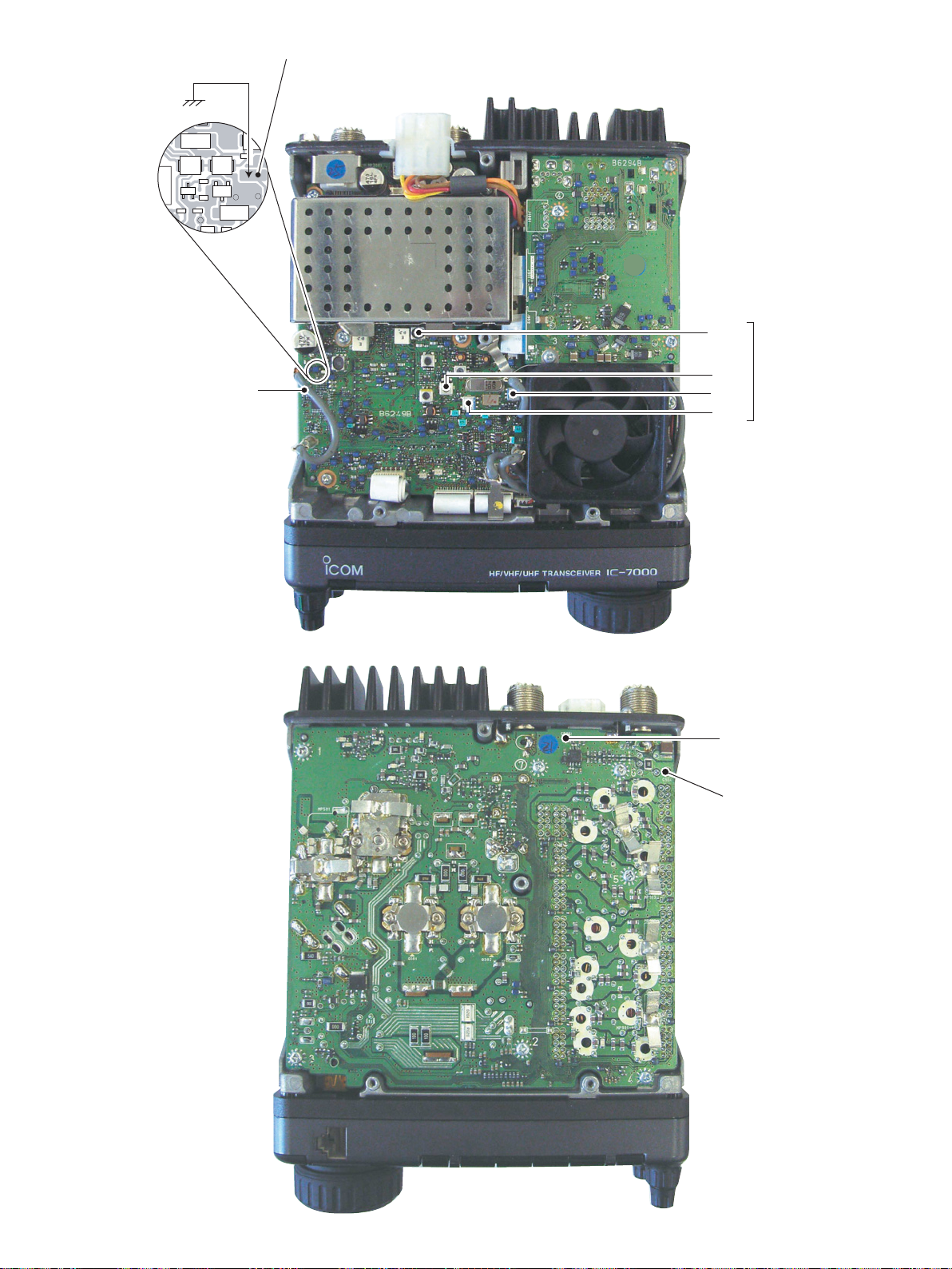
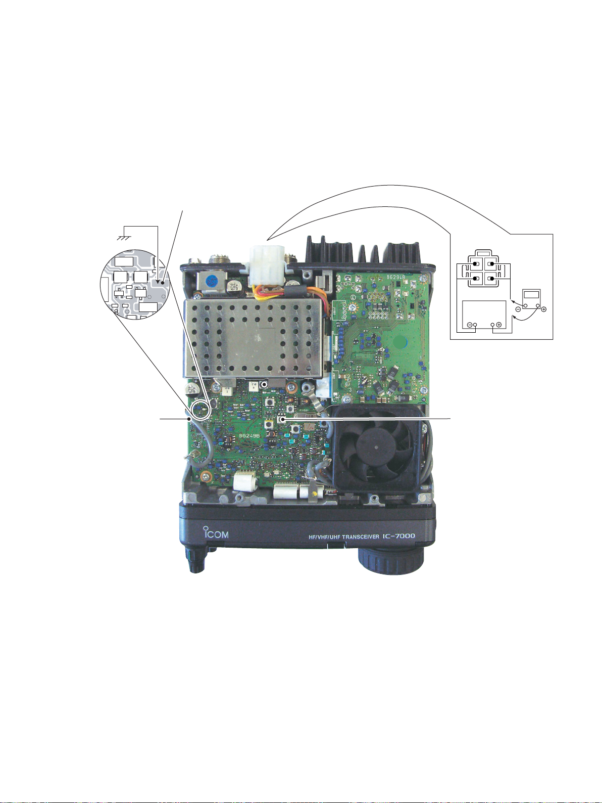
SECTION 2 INSIDE VIEWS
DDS UNIT
RX 1st mixer
(IC401: SPM5001)
YGR amplifier
(IC1:
PC2709T)
2nd Lo amplifier
(Q151*: 2SC4673)
3rd Lo DDS
(IC51*: AD9833BRM)
1st Lo DDS
(IC301*: AD9951YSV)
MAIN UNIT
LOGIC UNIT
RX 3rd mixer
(IC1301: TA4107F)
RX 2nd mixer
(D801: HSB88WS-E)
RF switch
(Q101: 2SC4213)
CPU
(IC1302: HD64F2377VFQ33V)
430 MHz pre amplifier
(Q451: 3SK291)
PA UNIT
144 MHz power amplifier
(Q501: RD70HVF1)
430 MHz power amplifier
(Q401: RD60HUF1)
DRIVER BOARD*
HF/50 MHz power amplifier
(Q301, Q302: RD70HHF1)
144 MHz pre amplifier
(Q551*: 3SK291)
LPF circuit
• TOP VIEW
LOGIC UNIT
LOGIC UNIT
MAIN UNIT
MAIN UNIT
CPU
CPU
(IC1302: HD64F2377VFQ33V)
(IC1302: HD64F2377VFQ33V)
RX 3rd mixer
TX 3rd mixer
(IC1301: TA4107F)
(IC1301: TA4107F)
2nd mixer
RX 2nd mixer
(D801: HSB88WS-E)
(D801: HSB88WS-E)
RF switch
RF switch
(Q101: 2SC4213)
(Q101: 2SC4213)
DDS UNIT
DDS UNIT
1st Lo DDS
1st Lo DDS
(IC301*: AD9951YSV)
(IC301*: AD9951YSV)
2nd Lo amplifier
2nd Lo amplifier
(Q151*: 2SC4673)
(Q151*: 2SC4673)
3rd Lo DDS
3rd Lo DDS
(IC51*: AD9833BRM)
(IC51*: AD9833BRM)
RX 1st mixer
1st mixer
(IC401: SPM5001)
(IC401: SPM5001)
YGR amplifier
YGR amplifier
(IC1: µPC2709T)
(IC1:
µPC2709T)
• BOTTOM VIEW
PA UNIT
PA UNIT
430 MHz pre amplifier
430 MHz pre amplifier
(Q451: 3SK291)
(Q451: 3SK291)
144 MHz power amplifier
144 MHz power amplifier
(Q501: RD70HVF1)
(Q501: RD70HVF1)
430 MHz power amplifier
430 MHz power amplifier
(Q401: RD60HUF1)
(Q401: RD60HUF1)
DRIVER BOARD*
DRIVER UNIT*
HF/50 MHz power amplifier
HF/50 MHz power amplifiers
(Q301, Q302: RD70HHF1)
(Q301, Q302: RD70HHF1)
2 - 1
144 MHz pre amplifier
144 MHz pre amplifier
(Q551*: 3SK291)
(Q551*: 3SK291)
LPF circuit
*Located under side of the point
LPF circuit
Page 6
SECTION 3 CIRCUIT DESCRIPTION
3-1 RECEIVER CIRCUITS
3-1-1 HF/50 MHz RF CIRCUIT (MAIN AND PA UNITS)
The HF/50 MHz RF filters pass only the desired band signals and suppress undesired band signals. The HF/50 MHz
RF circuit has 7 low-pass and 5 high-pass filters for specified band use.
The HF/50 MHz RF signals from the [ANT1] connector, pass
through one of 7 low-pass filters as below, the TX/RX switch
(PA unit; RL801), low-pass filter (PA unit; L801, L802, C801
–C805) and band switch (D151), and are then applied to the
MAIN unit via J101 (MAIN unit).
• Used RF low-pass fi lter (PA unit)
Frequency
(MHz)
0.03–2 MHz L1 RL881 15–22 MHz L5 RL941
2–4 MHz L2 RL921 22–30 MHz L6 RL821
4–8 MHz L3 RL841 30–60 MHz L7 RL861
8–15 MHz L4 RL901
The signals from the PA unit are applied to the RF switch
(Q101) via the band switch (D113) and then passed through
the 20 dB attenuator (D101, D102).
The signals below 1.8 MHz are passed through the low-pass
filter (L103, L104, C106, C110, C111) and then applied to
the preamplifier circuit.
The other band signals (1.8–60 MHz) are passed through
the high-pass filter (L105, L109, L110, L116, L117, C108,
C109, C114–C116) to suppress strong signals below
1.8 MHz and then applied to the low-pass and high-pass filter circuits.
(1) 1.8–2 MHz
The filtered signals from the high-pass filter are passed
through the low-pass filter (L205, L207, C209–C213) and
then applied to the preamplifier circuits.
(2) 2–30 MHz
The filtered signals from the high-pass filter are applied to
one of 5 high-pass filters as at right above after passed
through the low-pass filter (L205, L207, C209–C213) and
are then applied to the preamplifier circuit.
Control
signal
Entrance
relay
Frequency
(MHz)
Control
signal
Entrance
relay
• Used RF high-pass fi lter (MAIN unit)
Frequency
(MHz)
1.8–2 MHz B1 D204 13.9–20.9 MHz B5 D210
2–3.4 MHz B2 D205 20.9–30 MHz B6 D211
3.4–6.9 MHz B3 D208 30–60 MHz B7 D212
6.9–13.9 MHz B4 D209
Control
signal
Entrance
diode
Frequency
(MHz)
Control
signal
Entrance
diode
(3) 30–60 MHz
The filtered signals from the high-pass filter are passed
through another high-pass filter (L215, L217, C228, C229,
C237, C238) and then amplified at the RF amplifier (Q211).
The amplified signals are applied to the preamplifier circuit.
3-1-2 VHF AND UHF RF CIRCUITS (PA UNIT)
The VHF and UHF RF circuits filter and amplify only the
desired band signals and suppress undesired band signals.
The both RF circuits have preamplifiers and bandpass filters.
• VHF RF CIRCUIT
The VHF RF signals from the [ANT2] connector pass
through the low-pass filters (L506, L508, L510, L601–L603,
C516, C519, C521, C601, C602) and antenna switching circuit (D507–D509). The switched signals are passed through
the attenuator (D551, D552) and bandpass filter (D553,
D554, D556). The filtered signals are applied to the preamplifier (Q551) and then passed through another bandpass
filter (D558–D560).
The filtered signals are passed through the band switch
(D462) and then applied to the 1st mixer circuit (MAIN unit)
via J101 (MAIN unit).
• UHF RF CIRCUIT
The UHF RF signals from the [ANT2] connector pass
through the low-pass (L601–L603, C601, C602) and highpass (L413, L414, C428, C429, C431, C433) filters and
then applied to the antenna switching circuit (D408–D410).
The switched signals are passed through the attenuator
(D451, D452) and then amplified at the preamplifier (Q451)
between the 2 bandpass filters (D453–D456). The filtered
signals are amplified at another preamplifier (IC471, pins 1, 4).
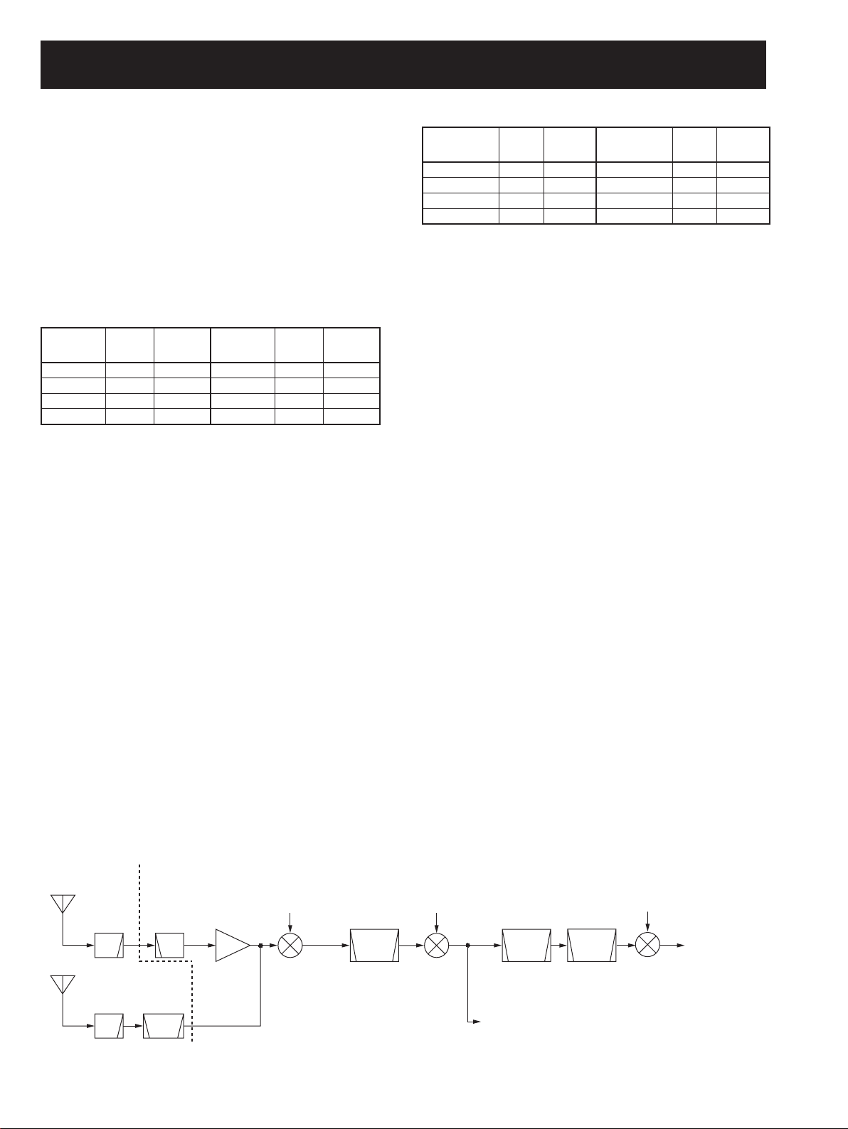
• RECEIVER CONSTRUCTION
PA UNIT
[ANT1]
0.03–60 MHz
LPF
[ANT2]
60–470 MHz
LPF
MAIN UNIT
HPF
BPF
Preamp.
Q301
amp.
1st LO:
124.517 MHz–
594.587 MHz
1st mixer
IC401
FI601
Crystal
filter
124.487 MHz
(WFM; 134.732 MHz)
3 - 1
2nd LO:
124.032 MHz
2nd mixer
D801
FI901
Crystal
filter
455 kHz
to WFM detector
circuit (IC1401)
FI1101
Crystal
filter
455 kHz
3rd LO:
438.85 kHz
to DSP circuit
3rd mixer
IC1101
Page 7

The amplified signals are passed through the band switch
(D461) and then applied to the 1st mixer circuit (MAIN unit)
via J101 (MAIN unit).
D453–D456, D553, D554, D556 and D558–D560 are
varactor diodes that tune the center frequency of an RF
passband for wide bandwidth receiving and good image
response rejection.
When receiving the signals, higher than 129 MHz, are
received, the switching diodes (D555, D557) are turned off
by the control signal “2MBL” from the CPU (LOGIC unit;
IC1302) via Q2150, then the varactor diodes (D556, D558)
are disconnected to shift the filtering frequencies.
3-1-3 PREAMPLIFIER CIRCUIT (MAIN UNIT)
The preamplifier circuit amplifies received RF signals for
wide band frequency range.
When the preamplifier is turned ON, the RF signals
(HF/50 MHz bands) from the high-pass filters are applied to
the preamplifier (Q301) via the preamplifier switches (D301,
D302).
When the preamplifier is turned OFF, the RF signals (HF/50
MHz bands) are passed through the bypass switches (D301,
D303).
The amplified or bypassed signals are applied to the 1st
mixer circuit (IC401).
3-1-4 1ST MIXER CIRCUIT (MAIN UNIT)
The 1st mixer circuit mixes the received RF signals with the
1st LO signal to convert the receive signal frequencies to
the 1st IF frequency.
3-1-5 1ST IF CIRCUIT (MAIN UNIT)
The 1st IF circuit filters and amplifies the 1st IF signal.
The converted 1st IF signal is
applied to the IF amplifier (Q502)
via RX switches (D502, D505).
The 124.487 MHz 1st IF signal
(except WFM mode) passes
through the crystal filter (FI601)
via the mode switches (D602,
• 1st IF frequency
Mode 1st IF
USB 124.48850 MHz
LSB 124.48550 MHz
CW 124.48700 MHz
RTTY 124.48683 MHz
AM/FM 124.48700 MHz
WFM 134.73200 MHz
D604), and the 134.732 MHz 1st
IF signal (WFM mode) passes through the bandpass filter
(L607, L609, C602, C606, C608–C610, C617, C618) via the
mode switches (D601, D603) to suppress out-of-band signals.
Then the filtered signal is applied to the IF amplifier (Q702)
and then applied to the 2nd mixer circuit (D801) via the RX
switches (D702, D704).
3-1-6 2ND MIXER CIRCUIT (MAIN UNIT)
The 2nd mixer circuit mixes the 1st IF signal with the 2nd
LO signal to convert into the 2nd IF frequency.
The amplified signal from the IF amplifier (Q702) is applied
to the 2nd mixer circuit (D801) and then mixed with the 2nd
LO signal (124.032 MHz) to convert into the 455 kHz (other
than WFM) or 10.7 MHz (WFM) 2nd IF signal.
The 2nd LO signal is generated in the DDS unit, and applied
to the 2nd mixer circuit (D801) after being filtered and
attenuated at the low-pass filter (L808, C816, C817) and the
attenuators (R801, R805, R806, R809–R811), respectively.
The converted 2nd IF signal is applied to the 2nd IF circuit.
While receiving the HF/50 MHz bands signals, the amplified
signals from the preamplifier switch (D304) or the bypassed
signals from the bypass switch (D303) are passed through
the low-pass filter (L310, L312, C314, C316, C318, C320,
C322) and then applied to the 1st mixer circuit (IC401) via
the band switch (D305).
While receiving the VHF/UHF bands signals, the signals
from the VHF/UHF RF circuit (PA unit) are passed through
the low-pass filter (L309, L311, L313, C313, C315, C317,
C319, C321, C323, C325) and then applied to the 1st mixer
circuit (IC401) via the band switch (D306).
The applied signals are mixed with the 1st LO signal (124.517
–594.487 MHz) and convert into the 1st IF signal.
The 1st LO signal is generated in the DDS unit, and applied
to the 1st mixer circuit (IC401, pins 1, 6) after being amplified and attenuated at the 1st LO amplifier (IC421, pins 1, 4)
and the attenuators (R416–R418, R421–R423), respectively.
The converted 1st IF signal is applied to the 1st IF circuit.
3-1-7 2ND IF CIRCUIT (MAIN UNIT)
The 2nd IF circuit amplifies and filters the 2nd IF signal.
The converted 2nd IF signal is applied to the bandpass filter
(FI901) to suppress undesired signals.
The 455 kHz 2nd IF signal (except
WFM mode) is passed through the
bandpass filter (FI901) via the mode
switch (D803) and then amplified
at the IF amplifier (Q902). The
amplified signal is passed through
the bandpass filter (FI1001) and
then applied to another IF amplifier
(Q1001).
The amplified signal is applied to the 3rd mixer circuit.
The 10.7 MHz 2nd IF signal for WFM mode is passed
through the low-pass filter (L1402, C1402–C1404) via
the mode switch (D802) and then applied to the IF amplifier (Q1401). The amplified signal is passed through the
bandpass filter (FI1401) and then applied another IF amplifier (Q1402).
• 2nd IF frequency
Mode 2nd IF
USB 456.500 kHz
LSB 453.500 kHz
CW 455.000 kHz
RTTY 454.830 kHz
AM/FM 455.000 kHz
WFM 10.700 MHz
3 - 2
Page 8
The amplified IF signal is passed through the bandpass filter
(FI1402) and then applied to the WFM demodulator circuit
(IC1401).
3-1-8 3RD MIXER CIRCUIT (MAIN UNIT)
The 3rd mixer circuit mixes the 2nd IF signal with the 3rd LO
signal to convert into the 3rd IF frequency.
The amplified signal from the IF amplifier (Q1001) are mixed
with the 3rd LO signal (438.85 kHz), where come from the
DDS unit via J2406, at the 3rd mixer circuit (IC1101) to convert into the 16.15 kHz 3rd IF signal.
The converted 3rd IF signal is applied to the 3rd IF circuit.
3-1-11 DSP CIRCUIT (LOGIC UNIT)
The DSP (Digital Signal Processor) circuit enables digital IF
filter, manual notch, digital twin PBT and phase demodulation, etc.
The 3rd IF or demodulated AF (WFM mode) signals are
passed through the low-pass filter (IC451, pins 1, 2) and
then applied to the A/D converter (IC551, pin 4). The converted signals are applied to the DSP ICs (IC301, IC2201)
for the digital IF filter, demodulation, automatic notch and
noise reduction, etc.
The output digital audio signals from the DSP IC (IC301) are
applied to the D/A converter (IC551) to convert into the analog audio signals.
3-1-9 3RD IF CIRCUIT (MAIN UNIT)
The 3rd IF circuit filters and amplifies the 3rd IF signal.
The converted 3rd IF signal is amplified at the 3rd IF amplifier (IC1203, pins 5, 7) and then passed through the lowpass filter (IC1203, pins 1, 3). The filtered signal is passed
through the mode switches (IC1201, pins 1, 7; IC1202, pins
1, 7) and then applied to the analog switch (IC1256, pins 11,
13).
The switched signal is applied to the DSP circuit (LOGIC
unit) via the J2251 (pin 1).
3-1-10 DEMODULATOR CIRCUITS (MAIN UNIT)
• WFM mode
The demodulator circuit converts the 2nd IF signal into the
AF signals.
The filtered signal from the bandpass filter (FI1402) is
applied to the IF amplifier section inside the WFM demodulator (IC1401, pin 1) and then applied to the quadrature
detector section to convert into AF signals. The detected AF
signals are output from pin 6 (IC1401) and then applied to
the mode switches (IC1201, pins 1, 7; IC1202, pins 1, 6).
The switched AF signals are applied to the analog
(IC1256, pins 11, 13) and then applied to the DSP circuit
(LOGIC unit) via J2251 (pin 1).
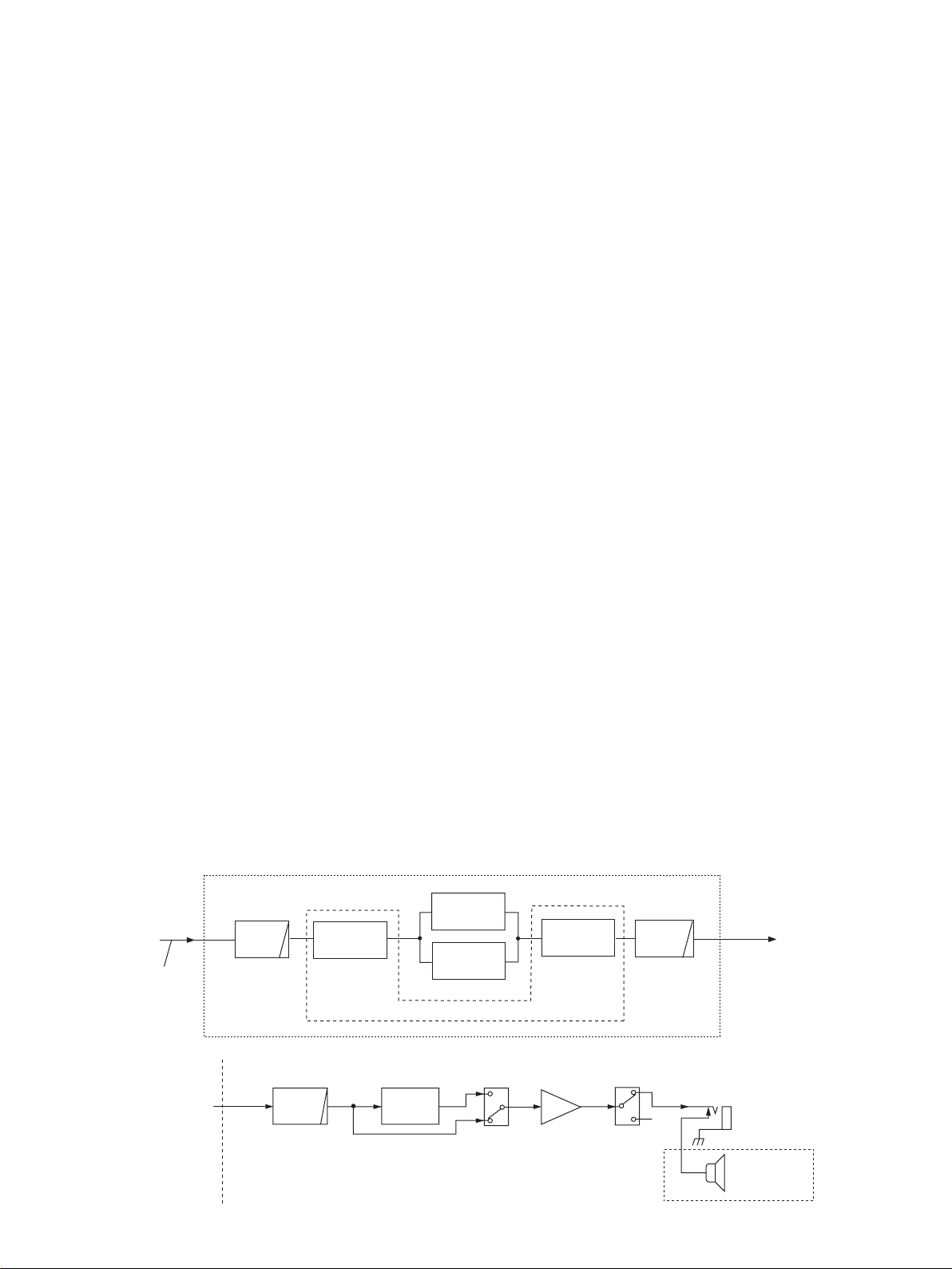
• DSP CIRCUIT
MAIN UNIT
3rd IF
signal
DSPI2
(16.15 kHz)
LOGIC unit
IC451
LPF
converter
switch
A/D
CODEC IC (IC551)
The converted audio signals from the D/A converter (IC551,
pins 25, 26) are passed through the low-pass filter (IC601,
pins 5–7), and then applied to the AF amplifier circuit (MAIN
unit) via J701 (pin 14).
3-1-12 AF AMPLIFIER CIRCUIT (MAIN UNIT)
The AF amplifier amplifies the demodulated AF signals to
drive speaker.
The filtered signal from the low-pass filter (LOGIC unit;
IC601, pins 5–7) are passed through another low-pass filter
(IC2551, pins 1, 3).
While in FM mode, the filtered AF signals from the low-pass
filter (IC2551, pin 1) are applied to the de-emphasis circuit
(IC2551, pins 5–7) to obtain the –6 dB/octave characteristics
and then applied to the AF switch (IC2601, pins 1, 6).
While except FM mode, the filtered AF signals from low-pass
filter (IC2551, pin 1) are applied to the AF switch (IC2601,
pins 1, 7).
The switched AF signals are amplified at the AF power
amplifier (IC2602, pins 1, 4) and then applied to the speaker
switch (Q2602).
The switched signal is applied to the internal speaker that is
connected to J2601 via [EXT SP] jack (J2602).
IC2201
DSP IC
D/A
converter
DSP IC
IC301
IC601
LPF
DSPO2
AF
signals
• AF CIRCUIT
DSPO1
LOGIC UNIT
IC2551
3
MAIN UNIT
LPF
IC2551
15
emphasis
De-
7
3 - 3
IC2601
6
7
6
1
AF amp.
IC2602
AF
Q2602
6
6
[EXT SP]
SP1
CHASSIS
Page 9
3-1-13 AGC CIRCUIT (MAIN UNIT)
The AGC (Automatic Gain Control) circuit adjusts IF amplify
gain to keep the audio output at a constant level. The
receiver gain is determined by the voltage on the AGC line
from the DSP circuit.
The AGC voltage is detected at the AGC detector section
inside the DSP ICs (LOGIC unit; IC301, IC2201) and the
AGC voltage is applied to the D/A converter (IC2155). The
converted AGC voltage is applied to the IF amplifiers (Q702,
Q902, Q1001) after being amplified at IC1201 (pin 12) and
sets the receiver gain with [RF/SQL] control.
When receiving strong signals, the detected voltage increases and the AGC voltage decreases. As the AGC voltage is
used for the bias voltage of the IF amplifiers (Q702, Q902,
Q1001), IF amplifier gain is decreased.
3-1-14 S-METER CIRCUIT (LOGIC UNIT)
The S-meter circuit indicates the relative received signal
strength while receiving.
The received signal strength is detected inside the DSP ICs
(IC301, IC2201) and then applied to the main CPU (IC1302).
The S-meter signal for WFM mode is output from the FM
detector IC (IC401, pin 4) and then applied to the to the
main CPU (IC1302, pin 123).
3-2 TRANSMITTER CIRCUITS
3-2-1 MICROPHONE AMPLIFIER CIRCUIT (MAIN UNIT)
The microphone amplifier circuit amplifies microphone audio
signal to a level needed for the DSP circuit.
Audio signals from the [MIC] connector (FRONT unit; J303
or MAIN unit; J2003) are amplified at the microphone amplifier (IC2007, pins 1, 2) and then applied to the DSP circuit
(LOGIC unit) via J2251 (pin 3).
3-2-2 DSP CIRCUIT (LOGIC UNIT)
The DSP (Digital Signal Processor) circuit enables digital
PSN modulator, digital Low Power modulator, digital Phase
modulator, transmitter monitor and side tone, etc.
The amplified microphone signals are passed through the
low-pass filter (IC502, pins 1, 2) and then applied to the A/D
converter (IC551, pin 3). The converted digital audio signal
are applied to the DSP ICs (IC301, IC2201) to covert into
the modulated 16.15 kHz 3rd IF signal. The modulated 3rd
IF signal from the DSP IC (IC301) is applied to the D/A convertor (IC551) to convert into the analog 3rd IF signal. The
converted analog 3rd IF signal is output from pins 27, 28
(IC551) and then passed through the low-pass filter (IC601,
pins 1–3).
The filtered IF signal is applied to the 3rd mixer circuit (MAIN
unit) via the J701 (pin 12).
The S-meter signal from the main CPU (IC1302) is applied
to the sub CPU (DISPLAY unit; IC2003) and is then displayed on the LCD display.
3-1-15 SQUELCH CIRCUIT (MAIN UNIT)
The squelch circuit mutes audio output when the S-meter
signal is lower than the [RF/SQL] control setting level.
The S-meter signal from the DSP IC is applied to the main
CPU (LOGIC unit; IC1302) and is compared with the threshold level set by the [RF/SQL] control. The [RF/SQL] setting
is picked up at the sub CPU (DISPLAY unit; IC2003, pin 74).
The main CPU (LOGIC unit; IC1302) compares the S-meter
signal and [RF/SQL] setting, and outputs the mute signal via
the DSP IC (IC301, pin B4) to the AF switch (IC2601, pin 2)
to cut AF signals via Q2607.
While receiving WFM mode, the S-meter signal is output
from the WFM demodulator (IC401, pin 4) and applied to the
to the main CPU (LOGIC unit; IC1302, pin 123). The main
CPU (LOGIC unit; IC1302) compares the S-meter signal and
[RF/SQL] setting, and outputs the mute signal via the DSP
IC (IC301, pin B4) to the AF switch (IC2601, pin 2) to cut AF
signals via Q2607.
• AGC CIRCUIT
DSPI1
IC1203
amp.
IF
3rd mixer
Q1001
amp.
IF
3-2-3 3RD MIXER CIRCUIT (MAIN UNIT)
The 3rd mixer circuit mixes the 3rd IF signal with the 3rd LO
signal to convert into the 2nd IF frequency.
The filtered signal from the low-pass filter (LOGIC unit;
IC601) is applied to the analog switch (IC2251, pins 1,
7) and then applied to the 3rd mixer circuit (IC1301, pins
3, 5). The applied signal is mixed with the 3rd LO signal
(438.85 kHz) coming from DDS unit via J2406 (pin 13) and
converted into the 455 kHz 2nd IF signal.
The converted 2nd IF signal is applied to the 2nd IF circuit.
3-2-4 2ND IF CIRCUIT (MAIN UNIT)
The 2nd IF circuit filters and amplifies the 2nd IF signal.
The converted 2nd IF signal is applied to the 2nd IF amplifier (Q901) and then passed through the bandpass filter
(FI901) via the TX switch (D903) to suppress unwanted signals.
The filtered signal is applied to the 2nd mixer circuit.
Q902
amp.
IF
2nd mixer
Q702
amp.
Q502
IF
amp.
IF
1st mixer
From the
antenna
DSP
CIRCUIT
IC301
IC2201
IC2155
D/A
converter
12
12
IC2101
AGC
14
3 - 4
Page 10
3-2-5 2ND MIXER CIRCUIT (MAIN UNIT)
The 2nd mixer circuit mixes the 2nd IF signal with the 2nd
LO signal to convert into the 1st IF frequency.
3-2-8 RF CIRCUIT (MAIN UNIT)
The RF circuit amplifies and filters the RF signal from the
1st mixer circuit.
The filtered signal from the bandpass filter (FI901) is applied
to the 2nd mixer circuit (D801) and mixed with 2nd LO signal (124.032 MHz) to convert into the 1st IF signal.
The 2nd LO signal is generated in the DDS unit, and applied
to the 2nd mixer circuit (D801) after being filtered and
attenuated at the low-pass filter (L808, C816, C817) and the
attenuators (R801, R805, R806, R809–R811), respectively.
The converted 1st IF signal is applied to the 1st IF circuit.
3-2-6 1ST IF CIRCUIT (MAIN UNIT)
The 1st IF circuit amplifies and filters the 1st IF signal.
The converted 1st IF signal is applied to the IF amplifier
(Q701) via the TX switch (D703) and then passed through
the bandpass filter (FI601) to suppress unwanted signals via
the filter switches (D601, D602).
The filtered signals are applied to the 1st mixer circuit.
3-2-7 1ST MIXER CIRCUIT (MAIN UNIT)
The 1st mixer circuit mixes the 1st IF signal with the 1st LO
signal to convert into the RF frequency.
The filtered signal is applied to the 1st mixer circuit (IC401)
via the TX switches (D501, D504) and mixed with the 1st LO
signal (124.517–594.487 MHz) to convert into the RF signal.
The 1st LO signal is generated in the DDS unit, and applied
to the 1st mixer circuit (IC401, pins 1, 6) after being amplified and attenuated at the 1st LO amplifier (IC421, pins 1, 4)
and the attenuators (R416–R418, R421–R423), respectively.
The converted RF signal is applied to the RF circuit.
The HF/50 MHz bands signal from the 1st mixer circuit
(IC401) is passed through the low-pass filter (L310, L312,
C314, C316, C318, C320, C322) via the band switch (D305).
The HF band signal is passed through one of 5 high-pass
(Refer to 3-1 for used RF high-pass filter) and low-pass
(L205, L207, C209–C213) filters.
The 50 MHz band signal is passed through the bandpass
filter (L219, L220, L246–L248, C240–C242, C282, C285–
C291).
The filtered HF/50 MHz bands signal is amplified at the YGR
amplifier (IC1) after passed through the high-pass filter (L109,
L110, L116, L117, C109, C114–C116) and attenuator (R5–
R7).
The amplified HF/50 MHz bands signal is applied to the
drive and power amplifier circuits (PA unit) via J1.
The VHF/UHF bands signal from the 1st mixer circuit (IC401)
is passed through the low-pass filter (L309, L311, L313,
C313, C315, C317, C319, C321, C323, C325) via the band
switch (D306).
The VHF band signal is passed through the bandpass filter
(L8, L10–L13, C18, C25, C26, C28, C29, C31–C33) via
the band switches (D3, D10) and then amplified at the RF
amplifier (IC2, pins 1, 3). The amplified signal is passed
through the band switch (D1) and attenuator (R5–R7), and
then applied to the YGR amplifier (IC1, pins 1, 4).
The amplified signal is passed through the high pass filter
(L21, C50–C52) via the filter switches (D6, D8) and then
applied to the drive and power amplifier circuits (PA unit) via
J1.
The UHF band signal is amplified at the RF amplifier (IC3,
pins 1, 3) via the band switch (D4) and passed through the
bandpass filters (FI2, FI3). The filtered signal is amplified at
the YGR amplifier (IC1, pins 1, 4) after passed through the
band switch (D2), attenuator (R5–R7) and bypass switches
(D7, D9).
• TRANSMITTER CONSTRUCTION
LOGIC UNIT (DSP circuit)
MIC
Controller
Q801
AMP.
MAIN UNIT
A/D
IC551
FI601
Crystal
BPF
594.487 MHz)
DSP
ICs
IC301
IC2201
1st mixer
IC401
1st LO
(124.517−
D/A
IC551
HPFs
BPF
The amplified signal is applied to the drive and power amplifier circuits (PA unit) via J1.
3rd LO
(438.85 kHz)
455 kHz
3 - 5
AMP.
IC504
DRIVER
UNIT
Q901
AMP.
124.487 MHz
HF/50 MHz
145 MHz
430 MHz
FI901
Ceramic
PA UNIT
PA
BPF
PA
(124.032 MHz)
2nd mixer
Q301
Q302
Q501
Q401
PA
2nd LO
D801
LPFs
ANT1
ANT2
Page 11
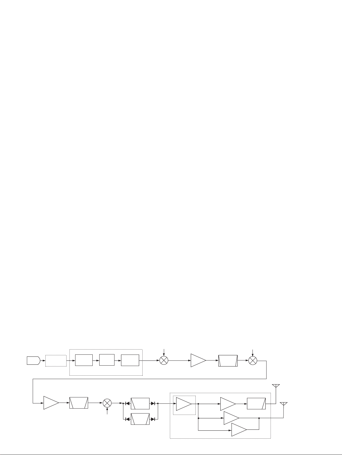
3-2-9 DRIVE AND POWER AMPLIFIER CIRCUITS
(PA AND DRIVER UNITS)
The drive and power amplifier circuits amplify the RF signal
from the RF circuit (MAIN unit) to obtain 100 W of RF output
power for the HF/50 MHz bands, 50 W for the VHF band
and 35 W for the UHF band.
The VHF and UHF RF power amplified signal from the
power amplifiers (PA unit; Q401, Q501) are detected at the
APC detectors (PA unit; D401, D404, D501, D504) respectively. The detected voltages ("VFOR" and "UFOR") are
combined to "VUFOR" voltage and then applied to the MAIN
unit.
The RF signal from the MAIN unit is applied to the pre drive
amplifiers (PA unit; Q101, Q102) after passed through the
attenuator (PA unit; R101–R103). The amplified signal is
applied to the drive amplifier (DRIVER unit; Q504) to amplify
a level needed for the power amplifiers.
The amplified HF/50 MHz bands signal from the drive amplifier is amplified at the power amplifiers (PA unit; Q301,
Q302) to obtain a stable 100 W of RF output power. The
power amplified signal is passed through the TX/RX switch
(RL801), one of the 7 low-pass filters, APC detector (PA
unit; D961, D962) and then applied to the [ANT1] connector
(CHASSIS; J1).
The amplified VHF RF signal from the drive amplifier is
amplified at the power amplifier (Q501) to obtain a stable
50 W of RF output power. The power amplified signals are
applied to the low-pass filter, APC detector (D501–D504),
TX/RX switch (D506, D510), low-pass filters (L506, L508,
L510, L601–L603, C516, C519, C521, C601, C602) and
[ANT2] connector (CHASSIS; J2).
The amplified UHF RF signal from the drive amplifier is
amplified at the power amplifier (Q401) to obtain a stable
35 W of RF output power. The power amplified signal is
applied to the low-pass filter, APC detector (D401–D404),
TX/RX switch (D406, D407), high-pass filter (L413, L414,
C428, C429, C431, C433), low-pass filter (L601–L603,
C601, C602) and [ANT2] connector (CHASSIS; J2).
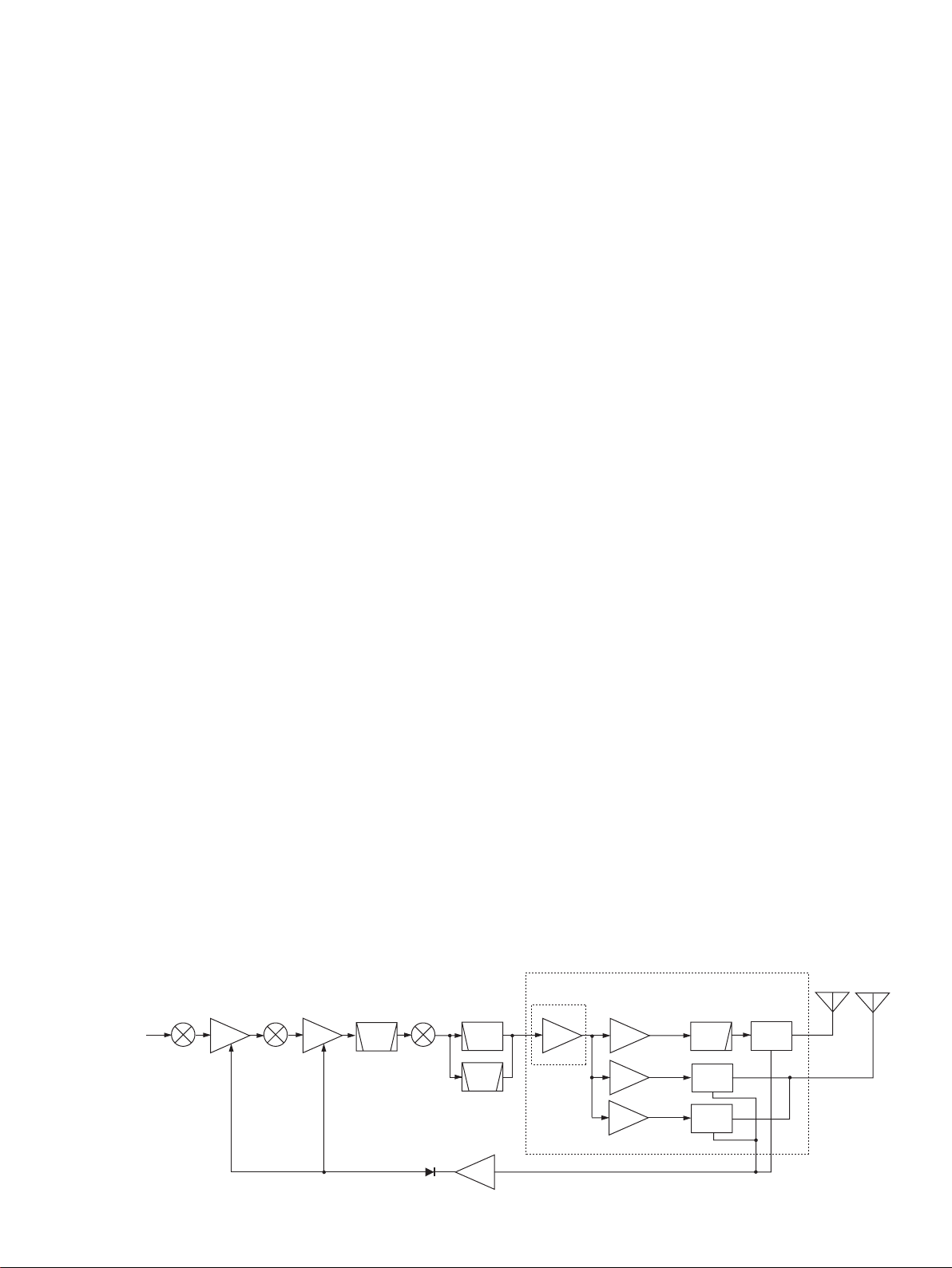
3-2-10 ALC CIRCUIT (MAIN UNIT)
The ALC (Automatic Level Control) circuit reduces the gain
of IF amplifiers in order for the transceiver to output a constant RF power set by the RF power setting even when the
supplied voltage shifts, etc.
The “HFOR” and “VUFOR” voltages are combined to the
“FORL” voltage and then applied to the ALC amplifier
(IC1601, pins 1, 2). The “POCV” voltage from the D/A converter (IC2155, pin 19) via the buffer amplifier (IC2101,
pins 5, 7), determined by the RF power setting, is applied to
the ALC amplifier (IC1601, pin 3) as the reference voltage.
When the “FORL” voltage exceeds the “POCV” voltage, ALC
bias voltage from IC1601 (pin 1) controls the IF amplifiers
(Q701, Q901). This adjusts the output power to the level
determined by the RF power setting until the “FORL” and
“POCV” voltages are equalized.
In AM mode, IC1601 functions as an averaging ALC amplifier with Q1601. The AM switch (Q1602) is turn ON and
shifts the “POCV” voltage to adjust the TX output power for
the AM mode (maximum; 40 W for HF/50 MHz bands, 20 W
for VHF band, 14 W for UHF band).
The ALC bias voltage from IC1601 is also applied to the
main CPU (LOGIC unit; IC1302, pin 115) as the “ALCL” voltage for ALC meter indication.
The external ALC input (negative voltage) from the [ACC]
socket (pin 6) is converted to a positive voltage at D1609
and is applied to the buffer amplifier (Q1604). External ALC
operation is identical to that of the internal ALC.
3-2-11 APC CIRCUIT (MAIN UNIT)
The APC (Automatic Power Control) circuit protects the
power amplifiers on the PA unit from high SWR and excessive current.
The reflected wave signal appears and increases on the
antenna connector when the antenna is mismatched.
The HF/50 MHz power amplified signal from the power
amplifiers (PA unit; Q301, Q302) is detected at the APC
detector (PA unit; D961). The detected voltage is applied
to the buffer amplifier (PA unit; IC960, pins 5, 7) and then
applied to the MAIN unit as the “HFOR” voltage.
• ALC CIRCUIT
TX
signals
3rd mixer 2nd mixer 1st mixer
Crystal
BPF
FI601
ALC amplifier
ALC
Q901
IF
IF
Q701
HPFs LPFs
BPF
1
ALC
IC1601
The HF/50 MHz reflected signal level is detected at D962 (PA
unit), and is amplified at the buffer amplifier (PA unit; IC960,
pins 1, 3) and applied to the ALC amplifier (IC1601, pins 8, 9)
as the "HREF" voltage.
ANT1
2
AMP PA
DRIVER
UNIT
HF/50 MHz
145 MHz
PA
430 MHz
PA
PA UNIT
APC
DET
APC
DET
APC
DET
3 - 6
ANT2
Page 12
The VHF/UHF APC detector circuits (PA unit; D501, D504,
D401, D404) detect the forward and reflection signals and
convert into DC voltages. The converted DC voltages are
combined and applied to the ALC amplifier (pins 1, 2) as
"VUFOR" voltage.
For the current APC, the driving current at the power amplifiers is detected in the voltages (“ICH” and “ICL”) which
appear at both terminals of detector resistors (PA unit; R721,
R722). The detected voltages are applied to the APC amplifier (IC1601, pins 5–7).
When the current of the power amplifier exceeds 22 A, The
output voltage from the APC amplifier (IC1601, pin 7) controls the ALC line to prevent excessive current flow.
3-2-12 RF, ALC, SWR METER CIRCUITS (LOGIC UNIT)
While transmitting, RF, ALC or SWR meter readings are
available and can be selected with the [F3 (MET)] switch.
(1) Power meter
The “FOR,” “VFOR” and “UFOR” voltages are combined to
the “FORL” voltage, and it is then applied to the main CPU
(IC1302, pin 113) for indicating the TX output power.
(2) ALC meter
The ALC bias voltage from the buffer amplifier (MAIN unit;
IC1601, pin 14) is applied to the main CPU (IC1302, pin 115)
via the “ALCL” signal line for indicating the ALC level.
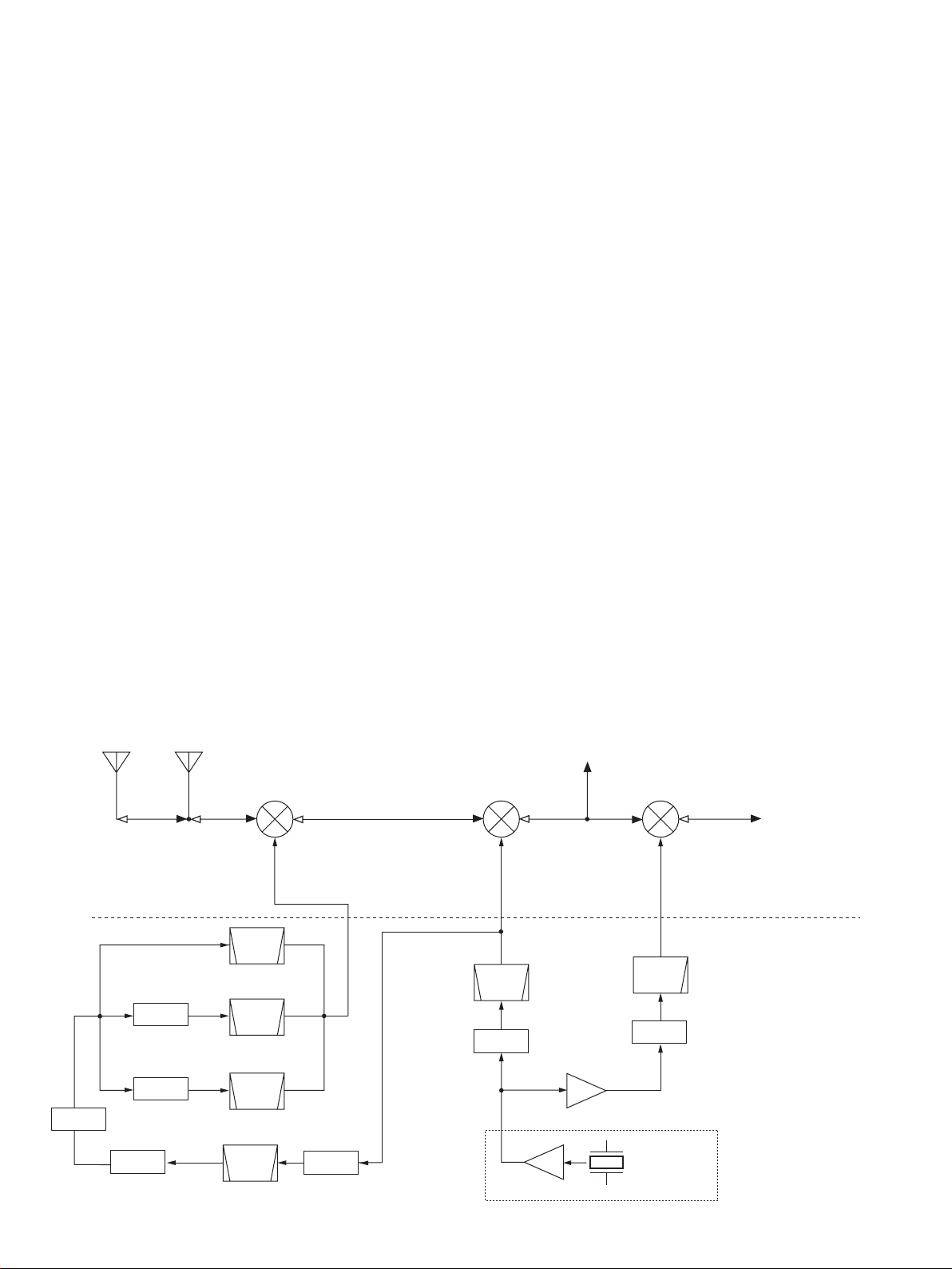
3-3 DDS CIRCUITS
3-3-1 GENERAL
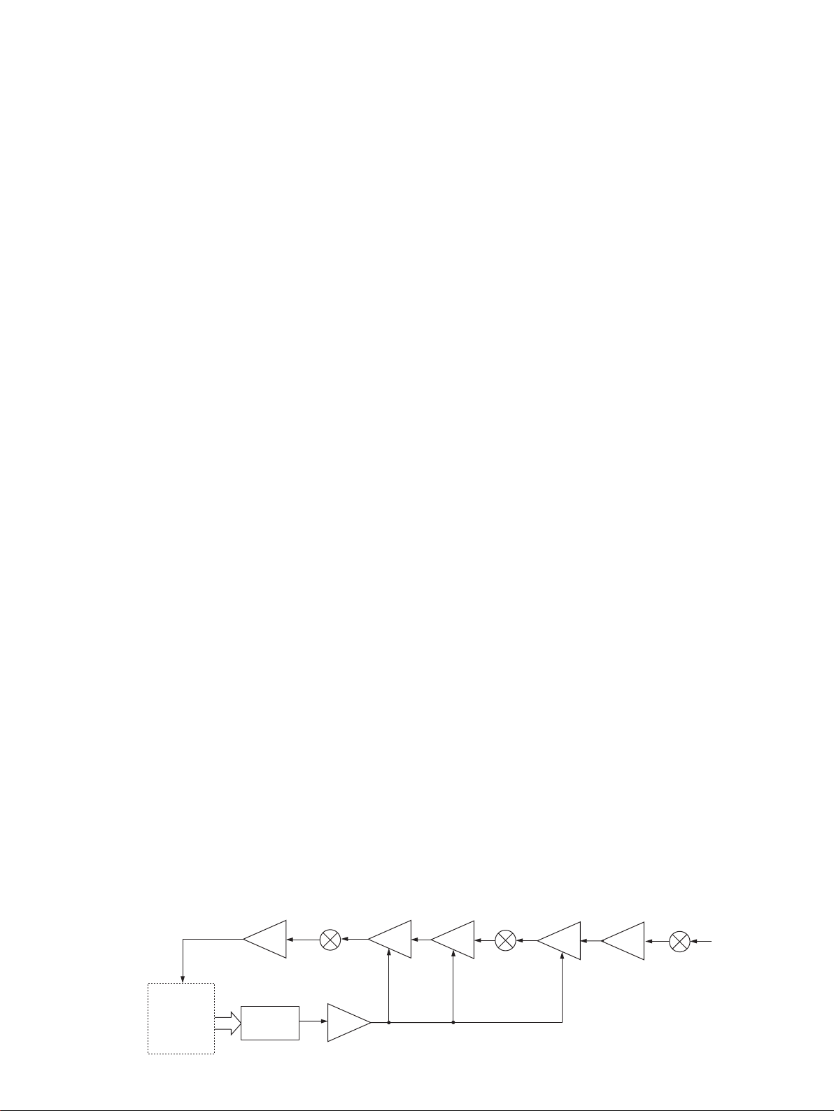
The DDS unit generates a 1st LO (124.517–594.487 MHz),
a 2nd LO (124.032 MHz) and a 3rd LO (438.85 kHz) frequencies.
3-3-2 1ST LO CIRCUIT (DDS UNIT)
The 1st LO circuit generates a 1st LO signal based on the
system clock that is tripled the 2nd LO frequency.
The 124.032 MHz 2nd LO signal is applied to the tripler
circuit (Q201) and then passed through the high-pass filter
(L205, L206, L210, C206–C210, C217–C219). The filtered
signal is amplified at Q211 and then passed through the
bandpass filter (FI201). The filtered signal is applied to the
DDS IC (IC301) as the 372.096 MHz system clock. The
DDS IC generates 38.62189–199.999999 MHz frequency
based on the system clock. The output signal from the DDS
IC (IC301, pins 20, 21) is applied to the doubler circuit
(D301) and then amplified at IC401 (pins 1, 4) after being
passed through the low-pass filter (L331, L332, C331, C332,
C335). The amplified signal is applied to one of the multiplier
circuits which is selected from the readout frequency and
then amplified at IC451 (pins 1, 5). The amplified signal is
passed through the bandpass filters.
The filtered signal is applied to the 1st mixer circuit (MAIN
unit) via J851.
(3) SWR meter
The “FORL” and “REFL” voltages are applied to the main
CPU (IC1302, pins 113, 114) respectively. The main CPU
compares the ratio of “FORL” to “REFL” voltage and indicates the SWR for the [ANT1] connector.
• FREQUENCY CONSTRUCTION
[ANT1]
0.03–
60 MHz
[ANT2]
60–
470 MHz
1st mixer
IC401
1st IF: 124.487 MHz
(WFM: 134.732 MHz)
124.517–
594.487 MHz
(1st LO)
MAIN UNIT
DDS UNIT
BPF
124.517–
154.486999 MHz
301
×2
×2
D456
×4
D471
DDS
IC301
372.096 MHz
(system clock)
BPF
154.487–
324.486999 MHz
BPF
524.487–
594.487 MHz
BPF
FI201
×3
Q201
2nd mixer
D801
124.032 MHz
BPF
×5
to WFM detector
(IC1401)
2nd IF: 455 kHz
(2nd LO)
FI101
Q101
AMP.
IC61
AMP.
Q1
3rd mixer
IC1101
LPF
DDS
Ref. Osc.
24.8064 MHz
X1
3rd IF: 16.15 kHz
to DSP circuit
438.85 kHz
(3rd LO)
IC51
24.8064 MHz
(system clock)
3 - 7
Page 13
3-3-3 2ND LO AND REFERENCE OSCILLATOR
CIRCUITS (DDS UNIT)
The reference oscillator (X1, Q1) generates a 24.8064 MHz
frequency used for the 1st LO, 3rd LO and DSP circuits as a
system clock and for the 2nd LO signal.
The oscillated signal is multiplied by 5 at Q101 and then
passed through the bandpass filter (FI101). The filtered
124.032 MHz signal is amplified at Q151 and then applied to
the 2nd mixer circuit (MAIN unit) after being passed through
the low-pass filter (L153, C154–C156) and attenuator (R157
–R159) via J151 as the 2nd LO signal.
3-3-4 3RD LO CIRCUIT (DDS UNIT)
The 3rd LO circuit generates a 3rd LO signal and shift the
frequency for the operating mode needed.
The DDS IC (IC51) generates a 10-bit digital signal. The
24.8064 MHz system clock signal from the reference oscillator (X1, Q1) is buffer amplified at IC61 (pins 2, 4) and then
applied to DDS IC (IC51, pins 5, 10). The DDS IC (IC51)
generates the 438.85 kHz frequency signal and then output
from pin 10. The output signal is applied to the low-pass filter (L53, C59–C61) and then applied to the 3rd mixer circuit
(MAIN unit) via J952 (pin 13) as the 3rd LO signal.
• 3RD LO FREQUENCY
Mode
USB 440.350 440.350
LSB 437.350 437.350
CW
CW-R
RTTY 436.555* 436.555*
RTTY-R 440.975* 436.555*
AM 438.850 438.850
FM 438.850 438.850
RX frequency
[kHz]
438.850
(–CW PITCH)
438.850
(+CW PITCH)
*RTTY TONE: 2125 Hz, RTTY SHIFT: 170 Hz
TX frequency
[kHz]
438.850
438.850
3-4 LOGIC CIRCUITS
3-4-1 BAND SELECTION DATA
IC2151
(MAIN)
Frequency
[MHz]
0.03–1.599999 B0
1.6–1.999999 B1
2.0–3.399999 B2
3.4–3.999999
4.0–6.899999
6.9–7.300000
7.300001–7.999999
8.0–10.999999
11.0–13.899999
13.9–14.350000
14.350001–
14.999999
15.0–20.899999
20.9–21.45
21.450001–
21.999999
22.0–29.999999
30.0–49.999999
54.000001–
59.999999
60.0–115.512999
115.513–
128.999999
129.0-148.0
148.000001–
199.999999
400.0–470.0 L9 L9 LOF6
IC2152
(MAIN)
HPF
(MAIN)
B3
B4
B5
B6
T: B1
R: B7
T: B1
R: B7
L8 L8
IC2152
(MAIN)
IC981
(PA)
LPF (PA)
L1
L2
L3
L4
L5
L6
L7 LOF250.0–54.0 B7
IC901
(DDS)
LOF
(DDS)
LOF1
LOF3
LOF4
LOF5
3-5 POWER SUPPLY CIRCUITS
3-5-1 FRONT UNIT VOLTAGE LINE
Line Description
Common 3.3 V converted from the 5 V line
3.3 V
5 V
3 - 8
by the 3.3 V regulator circuit (IC151). The output voltage is applied to the sub CPU (IC2003),
etc.
Common 5 V converted from the 8 V line by
the 5 V regulator circuit (IC101). The output
voltage is applied to the LCD driver (IC506),
etc.
Page 14

3-5-2 MAIN UNIT VOLTAGE LINE
Line Description
Common 3.3 V converted from the 5 V line
3.3 V
5 V
8 V
T8
R8
by the 3.3 V regulator circuit (IC1801). The
output voltage is applied to the D/A converter ICs (IC2151–IC5155), etc.
Common 5 V converted from the H V line by
the 5 V regulator circuit (IC1951). The output
voltage is applied to the CODEC IC (LOGIC
unit; IC551), low-pass filters (LOGIC unit;
IC451, IC502), etc.
Common 8 V line converted from the HV
line by the 8 V regulator circuit (IC1901).
The output voltage is applied to the buffer
amplifiers (IC2101–IC2103), analog switches
(IC2156, IC2251), etc.
Transmit 8 V controlled by the T8 regulator
circuit (Q1703, Q1704) using TXS signal
from the CPU (LOGIC unit; IC1302, pin
106). The output voltage is applied to the RF
switch (Q101), 2nd IF amplifier (Q701), 3rd
IF amplifier (Q901), etc.
Receive 8 V controlled by the R8 regulator
circuit (Q1701, Q1702) using RXS signal
from the CPU (LOGIC unit; IC1302, pin 105).
The output voltage is applied to the 2nd IF
amplifier (Q702), 3rd IF amplifier (Q1001),
3rd mixer (Q1101), etc.
3-6 PORT ALLOCATIONS
3-6-1 SUB-CPU (DISPLAY UNIT; IC2003)
Pin
number
3, 5
13, 14
15, 16
21 VRK Input port for [AF] switch.
22 PBTK Input port for [PBT/M-ch] switch.
23 TUNK Input port for [TUNER/CALL] key.
24 TSK Input port for [TS] key.
25 LCKK Input port for [LOCK] key.
26 BUPK Input port for [Y(BAND)] key.
27 BDNK Input port for [Z(BAND)] key.
28 FMSL
35 PHNK
37 LCK
Port
name
MDBK,
MDAK
S1AK,
S1BK
S2AK,
S2BK
Description
Input ports for [DIAL].
Input ports for [PBT2/M-ch] control.
Input ports for [PBT1/RIT] control.
Input port for the HM-151 connection
detection.
Input port for the headphones
connection detection.
Outputs clock signal for the LCD driver (IC506).
Pin
number
38 LDT
39 LDST
47 FSQS
48 RXD
54 BLV
55 KLV
56 TXD
57 PBT1D
58 PBT2D
70 LRXD
71 LTXD
73 AFGL Input port for [AF] control.
74 SQLL Input port for [RF/SQL] control.
75 PTTL
77 FUDL
78 KI0L
79 KI1L
80 KI2L
Port
name
Description
Outputs data signal for the LCD driver
(IC506).
Outputs strobe signal for the LCD
driver (IC506).
Outputs the squelch control signal.
High : Squelch is opened.
Outputs the RX LED control signal.
High : While receiving or squelch is
opened.
Outputs the dimmer control signal for
the LCD backlights.
Outputs the dimmer control signal for
the key backlights.
Outputs TX LED control signal.
Low : While transmitting.
Outputs control signal for [PBT/M-ch/
RIT] indicator.
Low : While the RIT function is ON.
Outputs control signal for [PBT/M-ch/
RIT] indicator.
Low : While the PBT function is ON.
Input port for data signal from the
main CPU (LOGIC unit; IC1302).
Outputs data signal to the main CPU
(LOGIC unit; IC1302).
Input port for PTT control signal from
the microphone that is connected to
the FRONT unit.
Input port for [UP] and [DN] switches from the optional microphone
(HM-103, SM-20) that is connected to
the FRONT [MIC] connector.
Input port for [MODE], [P.AMP/ATT],
[Y(MENU/GRP)] and [Z(MENU/
GRP)] keys.
Input port for [F-1], [F-2], [F-3] and
[F-4] keys.
Input port for [NB LEV], [NR LEV], [N/
ANF] and [SET/REC] keys.
3 - 9
Page 15

3-6-2 MAIN CPU (LOGIC UNIT; IC1302)
Pin
number
26 CYDT
27 CYCK
29 RTCDT
30 RTCCK
42 LOST
43 MST
46 MMDK
47 DRES
48 PRES#
49 SQSS
51 MCK
52 MDT
57 SDSS
58 TDAT
81 DTXD
82 DRXD
83 2T8V
104 4T8V
105 RXS
106 TXS
107 POWS
Port
name
Description
Outputs data signal for the clock generator (IC1201) for display control.
Outputs clock signal for the clock generator (IC1201) for display control.
I/O port for the data signal from/to the
clock IC (IC1304) for clock indication
and timer function.
Outputs clock signal for the clock IC
(IC1304) for clock indication and timer
function.
Outputs strobe signal for the D/A converter (DDS unit; IC901).
Outputs strobe signal for the D/A
converter ICs (MAIN unit; IC2151–
IC2154).
Input port for the data signal from the
microphone that is connected to the
rear [MIC] connector.
Outputs the reset signal for the DSP
ICs (IC301, IC2201).
Outputs the reset signal for the LCD
controller (IC1226) and DDS IC (DDS
unit; IC301).
Outputs the squelch control signal for
the ACC connector and connected
microphone.
Outputs clock signal for the D/A
converter ICs (MAIN unit; IC2151–
IC2154).
Outputs serial data signal for the D/A
converter ICs (MAIN unit; IC2151–
IC2154).
Outputs the signal for H SEND or V
SEND selection.
High : While V SEND is selected.
• Outputs data signal for AT-180.
• Outputs start signal for AH-3/AH-4.
Outputs data signal for the DSP IC
(IC301).
Input port for data signal from the
DSP IC (IC301).
Outputs the TX band signal.
High : While transmitting the 144 MHz
band.
Outputs the TX band signal.
High: While transmitting the 430 MHz
band.
Outputs R8 regulator (Q1701, Q1702)
control signal.
Low : While receiving.
Outputs T8 regulator (Q1703, Q1704)
control signal.
Low :While transmitting.
Outputs the power control signal .
High :When IC-7000 is power ON.
Pin
number
109 ECK
110 EDT I/O port for the EEPROM (IC1301).
113 FORL Input port for the forward voltage.
114 REFL Input port for the refl ection voltage .
115 ALCL Input port for ALC level.
116 SNDL
117 DPTL
118 THML
119 MUDL
121,
122
124 MMSL
127 TKEY Input port for tuner ON.
128 TRD
133 LTXD
134 LRXD
135 PWRK
137 3DST
138 PCK
140 1DST
142 PDT
Port name Description
Outputs clock signal to the EEPROM (IC1301).
Input port for PTT control signal
from the FRONT unit or ACC connector.
Input port for PTT control signal
from the DATA connector.
Input port for the temperature detection signal.
Input port for [UP] and [DN] switches from the optional microphone
(HM-103, SM-20) that is connected
to the rear [MIC] connector.
DASK,
DOTK
Input ports for [KEY] jack.
Input port for the HM-151 connection detection.
Input port for the detected signal for
the tuner unit connection.
Outputs data signal to the sub CPU
(DISPLAY unit; IC2003).
Inputs data signal from the sub
CPU (DISPLAY unit; IC2003).
Input port for [PWR] key.
Low : While [PWR] key is pushed.
Outputs strobe signal to the DDS
IC (DDS unit; IC51) for the 3rd LO
signal.
Outputs clock signal for the DDS
ICs (DDS unit; IC51, IC301) and
D/A converter (DDS unit; IC901).
Output strobe signal to the DDS IC
(DDS unit; IC301) for the 1st LO
signal.
Outputs serial data signal for the
DDS ICs (DDS unit; IC51, IC301)
and D/A converter (DDS unit;
IC901).
3 - 10
Page 16
SECTION 4 ADJUSTMENT PROCEDURES
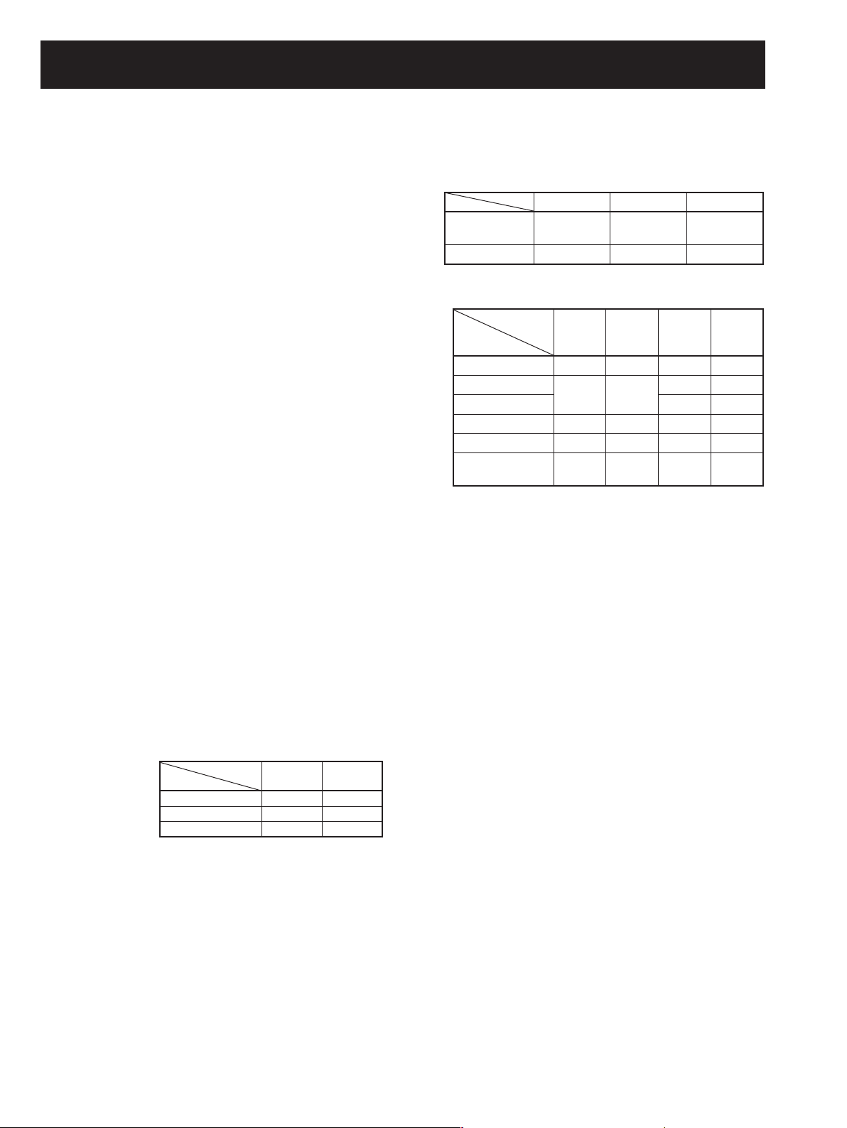
4-1 PREPARATION
Some adjustment must be performed on the adjustment mode.
M REQUIRED TEST EQUIPMENT
EQUIPMENT GRADE AND RANGE EQUIPMENT GRADE AND RENGE
DC power supply
RF power meter
(treminated type)
Frequency counter
RF voltmeter
Standard signal
generator (SSG)
Output voltage : 13.8 V DC
Current capacity : 30 A or more
Measuring range : 0.5–200 W
Frequency range : 1.8–500 MHz
Impedance : 50 Ω
SWR : 1.2 : 1 or better
Frequency range : 0.1–500 MHz
Frequency accuracy : ±1 ppm or better
Sensitivity : 100 mV or better
Frequency range : 0.1–500 MHz
Measuring range : 0.01–10 V
Frequency range : 0.1–500 MHz
Output level : 0.1 µV to 32 mV
(–127 to –17 dBm)
Distortion meter
Oscilloscope
Digital multimeter Imput impeadance : 10 MΩ/DC or more
AC millivoltmeter Measuring range : 10 mV to 10 V
DC voltmeter Input impedance : 50 kΩ/V DC or more
DC ammeter Measuring capability : 5 A/30 A
Audio generator
External speaker
M ENTERING THE ADJUSTMENT MODE
q Turn the transceiver’s power OFF.
w Connect the JIG plug (see illustration below) to [REMOTE] jack on the rear panel.
e While pushing and holding [P.AMP/ATT] and [TUNE/CALL], turn the transceiver power ON.
Frequency range : 1 kHz ±10 %
Measuring range : 1–100 %
Frequency range : DC–100 MHz
Measuring range : 0.01–10 V
Frequency range : 300–3000 Hz
Measuring range : 1–500 mV
Input impedance : 8 Ω
Capacity : 5 W or more
NOTE: Exiting from the adjustment mode when the transceiver's power is OFF.
[P.AMP/ATT]
Front panel
[TUNER/CALL]
[PWR]
M
OPERATING ON THE ADJUSTMENT MODE
• Enter DDS adjustment mode. : Push [F-1 (REF)]
• Enter TX adjustment mode. : Push [F-2 (TX)]
• Enter RX adjustment mode. : Push [F-3 (RX)]
• Store the set value. : Push [F-4 (SET)]
• Adjust the value. : Rotate [DIAL]
KEY ACC DATA
to [REMOTE] jack
Rear panel
2-conductor 3.5 (d) mm (1⁄8″) plug
MIC
GND
ANT2 ANT1
DC 13.8V
Shorten the both terminals
JIG plug
[DIAL]
CAUTION:
Connect a dummy load to the antenna con-
nectors during the transmitter adjustment,
when the adjustment condition does not require a test equipment.
4 - 1
[F-1(REF)]
[F-2 (TX)]
[F-3 (RX)]
[F-4 (SET)]
Page 17

• CONNECTION
• Microphone connector (Rear panel view)
NOTE! Connect the test equipment to the
micropho0ne connector on the rear panel,
otherwise the transmitter adjustment will not
adjusted properly.
AC
millivoltmeter
to [EXT SP]
Pin 5
MIC GND
Pin 6
MIC INPUT
18
DC power supply
AA13.8 V/30 A
Pin 7
GND
–
Audio
+
generator
+
–
Millivoltmerter
Pin 4
PTT
Ammeter
5 A, 30 A
to [MIC]
to [DC 13.8 V]
to [ANT 1/2]
Speaker
RF power meter
A200 W/50 Ω
Frequency counter
Standard signal
aagenerator
CAUTION!
DO NOT connect the
signal generator while
transmitting.
4 - 2
Page 18
4-2 DDS ADJUSTMENT
ADJUSTMENT ADJUSTMENT CONDITION DISPLAY OPERATION
REFERENCE
FREQUENCY
1 • Enter the adjustment mode.
• Push [F1 (REF)].
2• Disconnect P4 from J801 (MAIN
unit).
• Receiving
After the adjustment, exit the adjustment mode and connect P4 to J801 (MAIN unit).
4-3 DISPLAY ADJUSTMENT
ADJUSTMENT ADJUSTMENT CONDITION
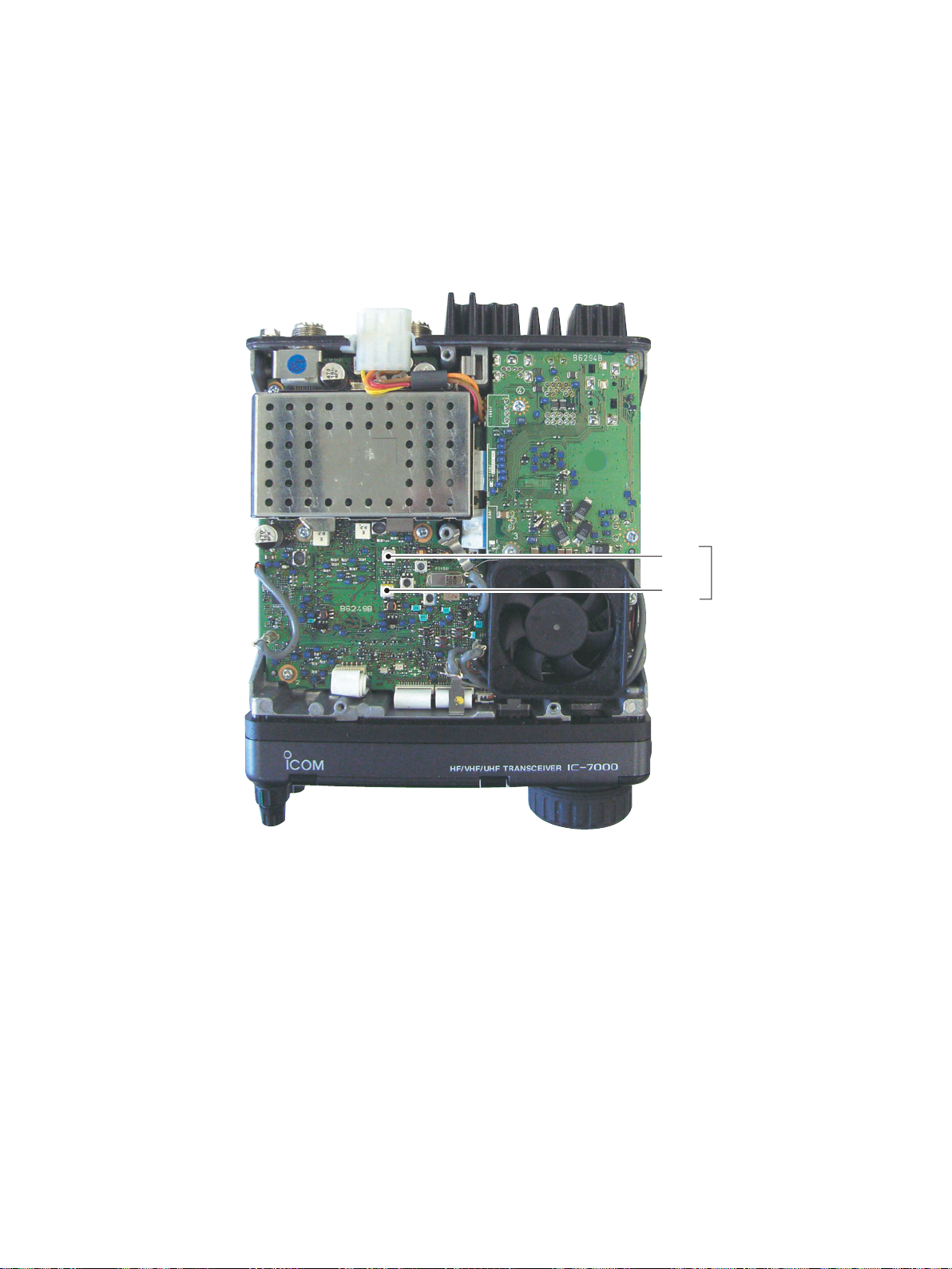
DISPLAY 1 • Connect between DISPLAY unit
ground and MAIN unit ground.
• Disconnect J2231 (MAIN unit).
• Receiving
2 • Receiving Connect a frequency
After the adjustment, connect J2231 (MAIN unit) and disconnect jumper wire between DISPLAY unit ground
and MAIN unit ground.
REF OSC
MEASUREMENT
UNIT LOCATION UNIT ADJUST
DIS-
PLAY
Connect a frequency
counter to CP536
through a capacitor
(0.0047 µF) and resistor
(1 kΩ) in series.
counter to CP505.
Connect a frequency counter to P4 and
set 124.032000 MHz using [DIAL]. Then
push [F-4 (SET)].
VALUE
3.579545 MHz
[USA]
4.433619 MHz
[Others]
15.734 kHz
[USA]
15.625 kHz
[Others]
ADJUSTMENT
DIS-
PLAY
DIS-
PLAY
C536
R541
4-4 TRANSMITTER ADJUSTMENT
ADJUSTMENT ADJUSTMENT CONDITION DISPLAY OPERATION
DRIVE/FINAL
IDLING
CURRENT
1 • Enter the adjustment mode.
• Push [F-2 (TX)].
2• Connect an RF power meter to
[ANT1] and [ANT2] connectors.
• Apply no audio signals to [MIC]
3 Rotate [DIAL] to set adjustment value to
jack.
• Connect a DC ammeter (5 A
type) between power supply and
4
transceiver.
• Transmitting
5 Rotate [DIAL] to set adjustment value to
6
7 Rotate [DIAL] to set adjustment value to
8
9 Rotate [DIAL] to set adjustment value to
10
11 Rotate [DIAL] to set adjustment value to
After the adjustment, exit the adjustment mode.
Driver Idle Cur
Final Idle Cur(HF/50M)-1
Final Idle Cur(HF/50M)-2
Final Idle Cur(144M)
Final Idle Cur(430M)
Preset the adjustment value to "00" using
with [DIAL], and check the driving current.
1 A value from the driving current of "00"
value. Then push [F-4 (SET )].
Preset the adjustment value to "00" using
with [DIAL], and check the driving current.
1 A value from the driving current of "00"
value. Then push [F-4 (SET )].
Preset the adjustment value to "00" using
with [DIAL], and check the driving current.
1 A value from the driving current of "00"
value. Then push [F-4 (SET )].
Preset the adjustment value to "00" using
with [DIAL], and check the driving current.
2 A value from the driving current of "00"
value. Then push [F-4 (SET )].
Preset the adjustment value to "00" using
with [DIAL], and check the driving current.
2.5 A value from the driving current of
"00" value. Then push [F-4 (SET )].
4 - 3
Page 19
• MAIN UNIT
Rear panel view
J2231
Display adjustment
presetting
Ammeter
DC power
supply
J801
P4
Reference frequency
check point
• FRONT UNIT
0.0047µF
1kΩ
CP536
Display check point
C536
Display adjustment point
Display check point
Frequency
counter
R541
Display adjustment point
CP505
4 - 4
Page 20
4-4 TRANSMITTER ADJUSTMENT (continue)
ADJUSTMENT ADJUSTMENT CONDITION
SWR
DETECTOR
TX PEAK 1 REAR
1 • Operating freq : 10.10000 MHz
• MODE : USB
• RF Power : 100%
• MIC Gain : 50%
2 PA Connect a DC voltmeter
• Connect an audio generator to
[MIC] connector and set as;
Frequency : 1.5 kHz
• Connect a wire between CP1601
(MAIN unit) and ground.
• Transmitting
After adjustment, disconnect the wire between CP1601 (MAIN unit) and ground.
• Operating freq. : 10.10000 MHz
• MODE : USB
• RF Power : 100%
• MIC Gain : 50%
• Preset R1618 (MAIN
unit) as the illustration at
right.
• Preset L604, L612
and L904 (MAIN
unit) as the illustration at right.
• Connect an audio generator to
[MIC] connector and set as ;
Level : 1.5 kHz/3 mV
( Adjust the audio generator
output level to keep less than
50 W output power.)
• Transmitting
Core’s
top
UNIT LOCATION UNIT ADJUST
REAR
panel
panel
MEASUREMENT
Connect an RF power
meter to [ANT1] connector.
to CP961.
Connect an RF power
meter to [ANT1] connector.
VALUE
80 W Audio
Minimum voltage
Maximum output power
ADJUSTMENT
genera-
tor
PA C964
MAIN L701
Output
level
ADJUSTMENT ADJUSTMENT CONDITION DISPLAY OPERATION
TX TOTAL
GAIN
1 • Enter the adjustment mode.
• Push [F-2 (TX)].
2• Connect an RF power meter to
[ANT1] connector.
• Connect an audio generator to
3
[MIC] connector and set as;
Level : 1.5 kHz/3 mV
4
• Transmitting
5
6• Connect an RF power to [ANT2]
connector.
• Transmitting
7
TX Total Gain(HF1)
TX Total Gain(HF2)
TX Total Gain(HF3)
TX Total Gain(50M)
TX Total Gain(144M)
TX Total Gain(430M)
Set the output power to 50 W using
[DIAL]. Then push [F-4 (SET)].
Set the output power to 50 W using
[DIAL]. Then push [F-4 (SET)].
Set the output power to 50 W using
[DIAL]. Then push [F-4 (SET)].
Set the output power to 50 W using
[DIAL]. Then push [F-4 (SET)].
Set the output power to 25 W using
[DIAL]. Then push [F-4 (SET)].
Set the output power to 17.5 W using
[DIAL]. Then push [F-4 (SET)].
4 - 5
Page 21
• MAIN UNIT
R1618
TX peak adjustment point
CP1601
SWR DETECTOR preset point
L904
L701
L604
L612
TX peak
adjustment point
• PA UNIT
CP961
SWR DETECTOR
check point
C964
SWR DETECTOR
adjustment point
4 - 6
Page 22

4-4 TRANSMITTER ADJUSTMENT (Continue)
ADJUSTMENT ADJUSTMENT CONDITION DISPLAY OPERATION
TX OUTPUT
POWER (HF)
APC (HF) 1
TX OUTPUT
POWER (AM)
TX OUTPUT
POWER
(50 MHz)
1• Connect an RF power meter to
[ANT1] connector.
• Connect an audio generator to
2
[MIC] connector and set as;
Level : 1.5 kHz/30 mV
3
• Transmitting
4
5
6
7
1• Connect an RF power meter to
[ANT1] connector.
• Apply no audio signal to [MIC]
connector.
• Transmitting
1• Connect an RF power meter to
[ANT1] connector.
• Connect an audio generator to
2
[MIC] connector and set as;
Level : 1.5 kHz/30 mV
3
• Transmitting
4
5
6
Po Min(HF)
Po Tune(HF)
Po 25%(HF)
Po 50%(HF)
Po(HF APC Low Volt)
Po 100%(HF)
Po Max(HF)
APC(HF)
AM POCV Ratio
Po Min(50 M)
Po Tune(50 M)
Po 25%(50 M)
Po 50%(50 M)
Po 100%(50 M)
Po Max(50 M)
Set the output power to 1 W using [DIAL].
Then push [F-4 (SET)] .
Set the output power to 10 W using
[DIAL]. Then push [F-4 (SET)].
Set the output power to 25 W using
[DIAL]. Then push [F-4 (SET)].
Set the output power to 50 W using
[DIAL]. Then push [F-4 (SET)].
Set the output power to 75 W using
[DIAL]. Then push [F-4 (SET)].
Set the output power to 95 W using
[DIAL]. Then push [F-4 (SET)].
Set the output power to 105 W using
[DIAL]. Then push [F-4 (SET)] key.
Push [F-4 (SET)].
Set the output power to 35 W using
[DIAL]. Then push [F-4 (SET)].
Set the output power to 1 W using [DIAL].
Then push [F-4 (SET)].
Set the output power to 10 W using
[DIAL]. Then push [F-4 (SET)].
Set the output power to 25 W using
[DIAL]. Then push [F-4 (SET)].
Set the output power to 50 W using
[DIAL]. Then push [F-4 (SET)].
Set the output power to 90 W using
[DIAL]. Then push [F-4 (SET)].
Set the output power to 100 W using
[DIAL]. Then push [F-4 (SET)].
4 - 7
Page 23
4-4 TRANSMITTER ADJUSTMENT (continue)
ADJUSTMENT ADJUSTMENT CONDITION DISPLAY OPERATION
TX OUTPUT
POWER
(144 MHz)
APC (VHF) 1
TX OUTPUT
POWER
(430 MHz)
1• Connect an RF power to [ANT2]
connector.
• Connect an audio generator to
2
[MIC] connector and set as;
Level : 1.5 kHz/30 mV
3
• Transmitting
4
5
1• Connect an RF power meter to
[ANT2] connector.
• Connect an audio generator to
2
[MIC] connector and set as;
Level : 1.5 kHz/30 mV
3
• Transmitting
4
5
Po Min(144 M)
Po 25%(144 M)
Po 50%(144 M)
Po 100%(144 M)
Po Max(144 M)
APC(VHF)
Po Min(430 M)
Po 25%(430 M)
Po 50%(430 M)
Po 100%(430 M)
Po Max(430 M)
Set the output power to 1 W using [DIAL].
Then push [F-4 (SET)].
Set the output power to 12.5 W using
[DIAL]. Then push [F-4 (SET)].
Set the output power to 25 W using
[DIAL]. Then push [F-4 (SET)].
Set the output power to 45 W using
[DIAL]. Then push [F-4 (SET)].
Set the output power to 50 W using
[DIAL]. Then push [F-4 (SET)].
Push [F-4 (SET)].
Set the output power to 1 W using [DIAL].
Then push [F-4 (SET)].
Set the output power to 8.75 W using
[DIAL]. Then push [F-4 (SET)].
Set the output power to 17.5 W using
[DIAL]. Then push [F-4 (SET)].
Set the output power to 31.5 W using
[DIAL]. Then push [F-4 (SET)].
Set the output power to 35 W using
[DIAL]. Then push [F-4 (SET)].
4 - 8
Page 24
4-4 TRANSMITTER ADJUSTMENT (continue)
ADJUSTMENT ADJUSTMENT CONDITION DISPLAY OPERATION
ALC 1 • Connect an RF power meter to
[ANT1] connector.
• Connect an audio generator to
[MIC] connector and set as;
Level : 1.5 kHz/30 mV
• Transmitting
Drive Min
(HF/50 MHz)
ALC (144 MHz) 1 • Connect an RF power meter to
Drive Min
(144 MHz)
ALC (430 MHz) 1 • Connect an RF power meter to
Drive Min
(430 MHz)
SWR 1 • Connect a 50 Ω dummy load to
1• Set an audio generator as;
Level : 1.5 kHz/20 mV
• Transmitting
[ANT2] connector.
• Connect an audio generator to
[MIC] connector and set as;
Level : 1.5 kHz/30 mV
• Transmitting
1• Set an audio generator as;
Level : 1.5 kHz/20 mV
• Transmitting
[ANT2] connector.
• Connect an audio generator to
[MIC] connector and set as;
Level : 1.5 kHz/30 mV
• Transmitting
1• Set an audio generator as;
Level : 1.5 kHz/20 mV
• Transmitting
[ANT1] connector.
• Transmitting
2• Connect a 100 Ω dummy load to
[ANT1] connector.
• Transmitting
After the adjustment, exit the adjustment mode.
ALC
Drive Min(HF/50 M)
ALC(144 M)
Drive Min(144 M)
ALC(430 M)
Drive Min(430 M)
SWR=1
SWR=2
Push [F-4 (SET)].
Push [F-4 (SET)].
Push [F-4 (SET)].
Push [F-4 (SET)].
Push [F-4 (SET)].
Push [F-4 (SET)].
Push [F-4 (SET)].
Push [F-4 (SET)].
ADJUSTMENT ADJUSTMENT CONDITION
ID APC 1
RESIDUALAM1 • Operating freq. : 10.10000 MHz
• Operating freq. : 18.10000 MHz
• MODE : USB
• Preset R1618 (MAIN
unit) as illustration at
right.
• Connect a wire between CP1601
(MAIN unit) and ground.
• Connect an RF power meter or
dummy load to [ANT1] connector.
• Connect an audio generator to
[MIC ] connector and set as;
Level : 1.5 kHz/30 mV
• Transmitting
After the adjustment, disconnect the wire between CP1601 and ground.
• MODE : FM
• Connect an audio generator to
[MIC] connector and set as;
Level : 1 kHz/30 mV
• Transmitting
MEASUREMENT
UNIT LOCATION UNIT ADJUST
REAR
panel
REAR
panel
Connect a DC ammeter
(30 A type) between the
DC power supply and
transceiver.
Connect an RF power
meter to [ANT1] connector.
4 - 9
VALUE
22 A MAIN R1618
Maximum
output power
ADJUSTMENT
MAIN L701
Page 25
• MAIN UNIT
CP1601
ID APC preset point
Rear panel view
Ammeter
DC power
supply
ID APC adjustment point
R1618
L701
Residual AM
adjustment point
4 - 10
Page 26

4-5 RECEIVER ADJUSTMENT
ADJUSTMENT ADJUSTMENT CONDITION
RX PEAK
(HF/50 MHz)
1 • Operating freq : 14.15000 MHz
• MODE : USB
• RIT : OFF
• AGC : FAST
• NB : OFF
• Preamp : ON
• Connect an SSG to [ANT1] connector and set as;
Frequency : 14.15150 MHz
Le vel : 500 µV* (–53 dBm)
Modulation : OFF
• Receiving
MEASUREMENT
UNIT LOCATION UNIT ADJUST
REAR
panel
Connect an AC
millivoltmeter to [EXT
SP] jack with an 8 Ω
load.
VALUE
Maximum AF
output level
ADJUSTMENT
MAIN L702,
L703
ADJUSTMENT ADJUSTMENT CONDITION DISPLAY
TOTAL GAIN
(HF/50 MHz)
S-METER
(HF/50 MHz)
RECEIVE
SENSITIVITY
(VHF/UHF)
*The output level of a standard signal generator (SSG) is indicated as SSG's open circuit.
1 • Enter the adjustment mode.
• Push [F-3 (RX)].
2• Connect an SSG to [ANT1] con-
nector and set as;
Level : 500 µV* (–53 dBm)
or OFF
Modulation : OFF
• Connect an AC millivoltmeter to
[EXT SP] jack with an 8 Ω load.
• Receiving
1• Connect an SSG to [ANT1] con-
nector and set as;
Frequency : 14.15150 MHz
Level : OFF
• Receiving
2• Set an SSG as;
Level : 50 µV* (–73 dBm)
• Receiving
3• Set an SSG as;
Level : 32 mV* (–17 dBm)
• Receiving
1• Connect an SSG to [ANT2] con-
nector and set as;
Frequency : 60.2015 MHz
Level : 10 µV* (–87 dBm)
Modulation : OFF
• Receiving
2• Set an SSG as ;
Frequency : 90.8015 MHz
• Receiving
3• Set an SSG as ;
Frequency : 128.8015 MHz
• Receiving
4• Set an SSG as ;
Frequency : 129.2015 MHz
• Receiving
5• Set an SSG as ;
Frequency : 145.3015 MHz
• Receiving
Total Gain(HF/50 M)
S0 Level
S9 Level
S9+60 Level
Tuned BPF(60 M)
Tuned BPF(90 M)
Tuned BPF(128 M)
Tuned BPF(129 M)
Tuned BPF(145 M)
Set 30 dB of AF level difference between
500 µV and no signal input from the SSG
using with [DIAL]. Then push [F-4 (SET)].
Push [F-4 (SET)].
Push [F-4 (SET)].
Push [F-4 (SET)].
Push [F-4 (SET)].
Push [F-4 (SET)].
Push [F-4 (SET)].
Push [F-4 (SET)].
Push [F-4 (SET)].
OPERATION
4 - 11
Page 27
• MAIN UNIT
L703
L702
RX peak
adjustment point
4 - 12
Page 28
4-5 RECEIVER ADJUSTMENT (continue)
ADJUSTMENT ADJUSTMENT CONDITION DISPLAY OPERATION
RECEIVE
SENSITIVITY
(VHF/UHF)
RX
TOTAL GAIN
(VHF/UHF)
S-METER
(WFM)
ADJUSTMENT ADJUSTMENT CONDITION
WFM
DISTORTION
6• Set an SSG as ;
Frequency : 169.8015 MHz
• Receiving
7• Set an SSG as ;
Frequency : 400.2015 MHz
• Receiving
8• Set an SSG as ;
Frequency : 435.2015 MHz
• Receiving
9• Set an SSG as ;
Frequency : 469.8015 MHz
• Receiving
1• Connect an SSG to [ANT2] con-
nector and set as;
Frequency : 435.2015 MHz
Level : 500 µV* (–53 dBm)
or OFF
Modulation : OFF
• Connect an AC millivolt meter to
[EXT SP] jack with an 8 Ω load.
• Receiving
1• Connect an SSG to the [ANT2]
connector and set as;
Frequency : 90.80 MHz
Leve l : 0.56 µV* (–112 dBm)
Modulation : OFF
• Receiving
2• Set an SSG as;
Level : 3.2 µV* (–97 dBm)
• Receiving
3• Set an SSG as;
Level : 32 µV* (–77 dBm)
• Receiving
After the adjustment, exit the adjustment mode.
1• Operating freq : 90.00000 MHz
MODE : WFM
Preamp : ON
• Connect an SSG to [ANT2] connector and set as;
Frequency : 90.0000 MHz
L evel : 3.2 µV* (–97 dBm)
Modulation : 1 kHz
Deviation : 50 kHz
• Receiving
Tuned BPF(170 M)
Tuned BPF(400 M)
Tuned BPF(435 M)
Tuned BPF(470 M)
Total Gain(144M/430M)
S0 Level(WFM)
S9 Level(WFM)
S9+60 Level(WFM)
MEASUREMENT
UNIT LOCATION UNIT ADJUST
REAR
panel
Connect a distortion meter to [EXT SP] jack with
an 8 Ω load.
Push [F-4 (SET)].
Push [F-4 (SET)].
Push [F-4 (SET)].
Push [F-4 (SET)].
Set 25 dB of AF level difference between
500 µV and no signal input from the SSG
using with [DIAL]. Then push [F-4 (SET)].
Push [F-4 (SET)].
Push [F-4 (SET)].
Push [F-4 (SET)].
VALUE
Minimum AF
distortion level
ADJUSTMENT
MAIN C1423
*The output level of a standard signal generator (SSG) is indicated as SSG's open circuit.
4 - 13
Page 29

• MAIN UNIT
WFM distortion
adjustment point
C1423
4 - 14
Page 30

SECTION 5 PARTS LIST
[REPLACEMENT UNITS]
ORDER NO. UNIT NAME
0324270102
0324270105
U 7000 #02 FRONT
U 7000 #05 FRONT
[EUR], [FRA], [ESP], [EXP], [UK]
[USA]
[FRONT UNIT]
REF ORDER
NO. N O.
DS1 5030002820 LCD LTA025A161A
W1 8900013940 CBL OPC-1447 (N=10, L=30)
W2 8900013990 CBL OPC-1445
EP1 880001670 UBD EX-2822 #01
DESCRIPTION
M.
H/V
LOCATION
[DISPLAY UNIT]
REF ORDER
NO. N O.
IC1 6910016730 S.DCC XC9504B092ARN B 44.4/9.4
IC101 1180001071 S.IC TA7805F (TE16L, Q) B 90.3/6.9
IC151 1180002201 S.IC RN5RZ33BA-TR-F B 99.9/4.8
IC301 1110002751 S.IC TA75S01F (TE85R, F) B 113.8/7.5
IC506 1120003010 S.IC AN2533FH-V B 69/38.5
IC651 1110005420 S.IC BA15532F-E2 B 4.1/25.6
IC2003 1140013140 S.IC HD64338020SB68HV B 93/26.3
IC2007 1110005821 S.IC R3112N281A-TR-F B 108.7/46.9
Q1 1550000090 S.FET RSQ035P03TR B 39.4/9.8
Q51 1560001330 S.FET RSR025N03 B 52.1/10.6
Q301 1560001290 S.FET 2SK3065 T100 T 110.8/31.4
Q302 1590003520 S.TR BCR108T T 116.7/10.2
Q303 1590003530 S.TR BCR08PN T 113.1/11.5
Q651 1590001650 S.TR XP4601 (TX) B 10.6/28.8
Q652 1590001650 S.TR XP4601 (TX) B 11.1/20.6
Q653 1590001650 S.TR XP4601 (TX) B 10.6/26.2
Q654 1590001650 S.TR XP4601 (TX) B 11.1/17
Q701 1530002060 S.TR 2SC4081 T106 R T 19.1/50.3
Q721 1530002060 S.TR 2SC4081 T106 R T 22/5.8
Q741 1530002060 S.TR 2SC4081 T106 R T 94/50.1
Q761 1530002060 S.TR 2SC4081 T106 R T 104.2/50.1
Q771 1530002060 S.TR 2SC4081 T106 R T 18.4/25.1
Q781 1530002060 S.TR 2SC4081 T106 R T 5.3/23.6
Q802 1520000460 S.TR 2SB1132 T100 R B 58.8/21.6
Q2001 1590003520 S.TR BCR108T B 81.6/23.7
Q2002 1590003570 S.TR BCR183T B 81.2/30.1
D1 1790000970 S.DIO MA729 (TX) B 36.8/10.1
D51 1750000730 S.DIO MA2SD1000L B 51/8
D301 1790001250 S.DIO MA2S111-(TX) B 111/32
D302 1790001520 S.ZEN MA8075-L (TX) B 109.9/7.6
D601 1750000950 S.DIO MA732 (TX) B 51.5/40
D602 1750000950 S.DIO MA732 (TX) B 53.3/40
D801 1730002340 S.ZEN MA8047-M (TX) B 35/40.4
D802 1730002340 S.ZEN MA8047-M (TX) B 39.8/25.8
D803 1730002340 S.ZEN MA8047-M (TX) B 38.6/22
D804 1730002340 S.ZEN MA8047-M (TX) B 41.8/23
D2001 1750000950 S.DIO MA732 (TX) T 107.4/26.5
D2002 1790001670 S.DIO RB706F-40T106 B 76.6/16.8
D2003 1790001670 S.DIO RB706F-40T106 T 116.4/36.7
D2004 1750000370 S.DIO DA221 TL T 100.6/41.8
D2005 1750000370 S.DIO DA221 TL B 101.7/42.8
D2006 1750000370 S.DIO DA221 TL B 107.3/5.9
X501 6050012140 S.XTL CR-805 [USA] B 87/43.5
6050012150 S.XTL CR-806 [Others] B 87/43.5
X2001 6050011550 S.XTL CR-747 B 106.5/27
DESCRIPTION
M.
H/V
LOCATION
[DISPLAY UNIT]
REF ORDER
NO. N O.
L1 6190001561 S.COL CDRH5D18NP-101NC B 68.4/6.3
L2 6190001561 S.COL CDRH5D18NP-101NC B 34.6/5.2
L3 6200002041 S.COL NLV25T-101J B 30.7/10.4
L51 6190001561 S.COL CDRH5D18NP-101NC B 55.9/6.2
L53 6200002041 S.COL NLV25T-101J B 60.9/10.9
L101 6200001831 S.COL NLV32T-100J B 96/11.6
L151 6200001831 S.COL NLV32T-100J B 96/8.6
L152 6200001831 S.COL NLV32T-100J B 100.6/11.4
L251 6200003950 S.COL HF50ACC 322513-T B 145.9/44
L252 6200003950 S.COL HF50ACC 322513-T B 146/50.6
L301 6200002041 S.COL NLV25T-101J B 109.6/16.7
L302 6200005011 S.COL NLV25T-100J T 112.6/24
L303 6200002041 S.COL NLV25T-101J T 112/20.3
L306 6200003261 S.COL NLV32T-101J T 109.8/25.5
L307 6200002041 S.COL NLV25T-101J T 115.4/26.6
L309 6200002041 S.COL NLV25T-101J T 115.3/24
L310 6200002041 S.COL NLV25T-101J T 115.4/21.5
L312 6200002041 S.COL NLV25T-101J T 115.4/19
L313 6200002041 S.COL NLV25T-101J T 115.7/16.3
L505 6200005521 S.COL NLV25T-470J B 71.2/47.9
L506 6200005011 S.COL NLV25T-100J B 67.9/20.2
L507 6200005011 S.COL NLV25T-100J B 50.2/29
L508 6200005011 S.COL NLV25T-100J B 49.3/24.3
L509 6200005011 S.COL NLV25T-100J B 17.4/35.6
L601 6200002041 S.COL NLV25T-101J B 70.6/25.2
L602 6200005011 S.COL NLV25T-100J B 53.5/36.2
L603 6200005011 S.COL NLV25T-100J B 51/43.6
L604 6200005011 S.COL NLV25T-100J B 53.5/43.6
L605 6200005011 S.COL NLV25T-100J B 50.9/36.2
L651 6200002041 S.COL NLV25T-101J B 19.1/42.7
L701 6200002041 S.COL NLV25T-101J B 21.1/37.5
L702 6200002041 S.COL NLV25T-101J B 65.4/10.9
L703 6200002041 S.COL NLV25T-101J B 27.9/11.3
L801 6200005011 S.COL NLV25T-100J B 63.4/16.9
L802 6200002041 S.COL NLV25T-101J B 19.1/47.5
L851 6200003950 S.COL HF50ACC 322513-T B 33.2/17.2
L852 6200003950 S.COL HF50ACC 322513-T B 35/21.3
L853 6200002041 S.COL NLV25T-101J B 34.4/26.6
L854 6200002041 S.COL NLV25T-101J B 34.4/24.1
L855 6200003950 S.COL HF50ACC 322513-T B 36.4/17.2
R1 7030008141 S.RES ERA3YKD 224V (220 kΩ) B 33.4/9.6
R2 7030005671 S.RES ERA3YKD 393V (39 kΩ) B 33.4/11.6
R3 7030008051 S.RES ERA3YKD 184V (180 kΩ) B 42.6/6.4
R4 7030005050 S.RES ERJ2GEJ 103 X (10 kΩ) B 40.9/6.8
R5 7030005050 S.RES ERJ2GEJ 103 X (10 kΩ) B 40.9/7.7
R51 7030008141 S.RES ERA3YKD 224V (220 kΩ) B 49.7/10.8
R52 7030007911 S.RES ERA3YKD 563V (56 kΩ) B 48.5/10.8
R53 7030006561 S.RES ERA3YED 223V (22 kΩ) B 46.5/11.8
R54 7030005050 S.RES ERJ2GEJ 103 X (10 kΩ) B 47.9/8.4
R55 7030005050 S.RES ERJ2GEJ 103 X (10 kΩ) B 48.8/8.4
R201 7030010040 S.RES ERJ2GEJ-JPW B 109.6/38
R202 7030010040 S.RES ERJ2GEJ-JPW B 109.6/39
R251 7030005120 S.RES ERJ2GEJ 102 X (1 kΩ) B 136.5/49.6
R252 7030000300 S.RES MCR10EZHJ 220 Ω B 133.9/47.3
R253 7030000300 S.RES MCR10EZHJ 220 Ω B 142/50.8
R254 7030000300 S.RES MCR10EZHJ 220 Ω B 133.9/49
R255 7030000300 S.RES MCR10EZHJ 220 Ω T 143.2/50.7
R301 7030005120 S.RES ERJ2GEJ 102 X (1 kΩ) B 113.2/32
R302 7030005050 S.RES ERJ2GEJ 103 X (10 kΩ) T 114/30.4
R303 7030005120 S.RES ERJ2GEJ 102 X (1 kΩ) B 111/33.4
R304 7030007300 S.RES ERJ2GEJ 332 X (3.3 kΩ) B 111.9/33.4
R305 7030007300 S.RES ERJ2GEJ 332 X (3.3 kΩ) B 113.2/32.9
R306 7030005120 S.RES ERJ2GEJ 102 X (1 kΩ) T 114.9/11
R307 7030005050 S.RES ERJ2GEJ 103 X (10 kΩ) B 111.3/8.4
R308 7030005230 S.RES ERJ2GEJ 334 X (330 kΩ) B 113.8/5.3
R309 7030005310 S.RES ERJ2GEJ 124 X (120 kΩ) B 112/5.3
R310 7030008010 S.RES ERJ2GEJ 123 X (12 kΩ) B 110.2/5.3
R521 7030008370 S.RES ERJ2GEJ 561 X (560 Ω) B 60.8/46.1
R522 7030010040 S.RES ERJ2GEJ-JPW B 65.3/47.4
R523 7030010040 S.RES ERJ2GEJ-JPW B 65.4/48.7
R524 7030010900 S.RES ERJ3GEYJ 750 V (75 Ω) B 63.1/48.9
R528 7030010040 S.RES ERJ2GEJ-JPW B 60.8/42.6
R529 7030005050 S.RES ERJ2GEJ 103 X (10 kΩ) B 58.6/43.8
R530 7030005080 S.RES ERJ2GEJ 823 X (82 kΩ) B 60.8/43.6
R531 7030009290 S.RES ERJ2GEJ 562 X (5.6 kΩ) B 76.3/42.9
R532 7030005050 S.RES ERJ2GEJ 103 X (10 kΩ) B 60.8/37.2
R533 7030010040 S.RES ERJ2GEJ-JPW B 56.5/32.3
R534 7030010040 S.RES ERJ2GEJ-JPW B 60.8/36
R536 7030010040 S.RES ERJ2GEJ-JPW B 62.6/29
R537 7030010040 S.RES ERJ2GEJ-JPW B 64.6/29
R538 7030010040 S.RES ERJ2GEJ-JPW B 66.6/29
DESCRIPTION
M.=Mounted side (T: Mounted on the Top side, B: Mounted on the Bottom side)
S.=Surface mount
M.
H/V
LOCATION
5 - 1
Page 31

[DISPLAY UNIT]
REF ORDER
NO. N O.
R539 7030005720 S.RES ERJ2GEJ 563 X (56 kΩ) B 69.6/29
R540 7030010040 S.RES ERJ2GEJ-JPW B 68.6/29
R541 7310004650 S.TRI EVM-2WSX80 B53 B 53.3/49.2
R544 7030010040 S.RES ERJ2GEJ-JPW B 60.8/39.6
R545 7030005720 S.RES ERJ2GEJ 563 X (56 kΩ) B 60.8/32
R546 7030010040 S.RES ERJ2GEJ-JPW B 60.8/34
R547 7030010040 S.RES ERJ2GEJ-JPW B 59.2/34.8
R548 7030010040 S.RES ERJ2GEJ-JPW B 60.8/33
R549 7030010040 S.RES ERJ2GEJ-JPW B 63.6/29
R550 7030010040 S.RES ERJ2GEJ-JPW B 65.6/29
R551 7030010040 S.RES ERJ2GEJ-JPW B 67.6/29
R553 7030010040 S.RES ERJ2GEJ-JPW B 59.5/43.8
R601 7030008410 S.RES ERJ2GEJ 392 X (3.9 kΩ) B 72.7/24.9
R602 7030008410 S.RES ERJ2GEJ 392 X (3.9 kΩ) B 74.5/24.9
R603 7030008410 S.RES ERJ2GEJ 392 X (3.9 kΩ) B 75.4/24.9
R604 7030008410 S.RES ERJ2GEJ 392 X (3.9 kΩ) B 77.2/24.9
R605 7030008410 S.RES ERJ2GEJ 392 X (3.9 kΩ) B 75.3/30.2
R606 7030008410 S.RES ERJ2GEJ 392 X (3.9 kΩ) B 76.3/24.9
R608 7030010040 S.RES ERJ2GEJ-JPW B 48.8/36.8
R609 7030005040 S.RES ERJ2GEJ 472 X (4.7 kΩ) B 48.8/45.3
R610 7030010040 S.RES ERJ2GEJ-JPW B 48.8/42.3
R612 7030005040 S.RES ERJ2GEJ 472 X (4.7 kΩ) B 48.8/43.3
R651 7030005050 S.RES ERJ2GEJ 103 X (10 kΩ) B 5.5/19.6
R652 7030005220 S.RES ERJ2GEJ 223 X (22 kΩ) B 0.8/25.7
R653 7030005060 S.RES ERJ2GEJ 333 X (33 kΩ) B 5.5/21.4
R654 7030005070 S.RES ERJ2GEJ 683 X (68 kΩ) B 0.8/23.9
R655 7030005090 S.RES ERJ2GEJ 104 X (100 kΩ) B 4.1/30.7
R656 7030005110 S.RES ERJ2GEJ 224 X (220 kΩ) B 0.8/27.4
R657 7030005060 S.RES ERJ2GEJ 333 X (33 kΩ) B 1.8/30.3
R658 7030005090 S.RES ERJ2GEJ 104 X (100 kΩ) B 4.1/29.8
R659 7030003600 S.RES ERJ3GEYJ 223 V (22 kΩ) B 8.4/28.5
R660 7030005720 S.RES ERJ2GEJ 563 X (56 kΩ) B 13.2/29.9
R661 7030005220 S.RES ERJ2GEJ 223 X (22 kΩ) B 13.7/27.1
R662 7030007350 S.RES ERJ2GEJ 393 X (39 kΩ) B 13.7/28.7
R663 7030005220 S.RES ERJ2GEJ 223 X (22 kΩ) B 13.2/20.6
R664 7030007340 S.RES ERJ2GEJ 153 X (15 kΩ) B 5.7/29.8
R665 7030003600 S.RES ERJ3GEYJ 223 V (22 kΩ) B 8.9/20.6
R666 7030004980 S.RES ERJ2GEJ 101 X (100 Ω) B 13.1/25.3
R667 7030004980 S.RES ERJ2GEJ 101 X (100 Ω) B 11.1/18.8
R668 7030004980 S.RES ERJ2GEJ 101 X (100 Ω) B 9.7/24.2
R669 7030004980 S.RES ERJ2GEJ 101 X (100 Ω) B 13.6/16.2
R701 7030004990 S.RES ERJ2GEJ 221 X (220 Ω) T 18.4/48
R702 7030007280 S.RES ERJ2GEJ 331 X (330 Ω) T 19.7/48
R703 7030007290 S.RES ERJ2GEJ 222 X (2.2 kΩ) T 25.1/41
R704 7030005040 S.RES ERJ2GEJ 472 X (4.7 kΩ) T 16.6/17.2
R705 7030007340 S.RES ERJ2GEJ 153 X (15 k
R721 7030004990 S.RES ERJ2GEJ 221 X (220 Ω) T 20.2/6.2
R722 7030007280 S.RES ERJ2GEJ 331 X (330 Ω) T 23.8/5.6
R723 7030003480 S.RES ERJ3GEYJ 222 V (2.2 kΩ) T 47.5/2.4
R724 7030003520 S.RES ERJ3GEYJ 472 V (4.7 kΩ) T 61.8/2.4
R725 7030003580 S.RES ERJ3GEYJ 153 V (15 kΩ) T 75.9/2.4
R741 7030004990 S.RES ERJ2GEJ 221 X (220 Ω) T 92.2/49.7
R742 7030007280 S.RES ERJ2GEJ 331 X (330 Ω) T 95.7/49.6
R743 7030007290 S.RES ERJ2GEJ 222 X (2.2 kΩ) T 102.1/35
R744 7030005040 S.RES ERJ2GEJ 472 X (4.7 kΩ) T 102.1/25.5
R745 7030007340 S.RES ERJ2GEJ 153 X (15 kΩ) T 100.6/8.6
R761 7030004990 S.RES ERJ2GEJ 221 X (220 Ω) T 103.1/48.2
R762 7030007280 S.RES ERJ2GEJ 331 X (330 Ω) T 104.8/47.8
R771 7030004990 S.RES ERJ2GEJ 221 X (220 Ω) T 18.7/28.9
R772 7030007280 S.RES ERJ2GEJ 331 X (330 Ω) T 18.1/29.9
R781 7030004990 S.RES ERJ2GEJ 221 X (220 Ω) T 3.5/22.4
R782 7030007280 S.RES ERJ2GEJ 331 X (330 Ω) T 3.5/24.2
R801 7030005240 S.RES ERJ2GEJ 473 X (47 kΩ) B 62/21.8
R802 7030007270 S.RES ERJ2GEJ 151 X (150 Ω) B 62/20
R803 7030005120 S.RES ERJ2GEJ 102 X (1 kΩ) B 62/23.6
R2002 7030005240 S.RES ERJ2GEJ 473 X (47 kΩ) T 110.4/40.7
R2003 7030005050 S.RES ERJ2GEJ 103 X (10 kΩ) T 24.6/24.3
R2004 7030005050 S.RES ERJ2GEJ 103 X (10 kΩ) T 24.6/26.3
R2005 7030005050 S.RES ERJ2GEJ 103 X (10 kΩ) T 24.6/23.3
R2006 7030005050 S.RES ERJ2GEJ 103 X (10 kΩ) T 24.6/25.3
R2007 7030007290 S.RES ERJ2GEJ 222 X (2.2 kΩ) T 107.6/24.4
R2008 7030005220 S.RES ERJ2GEJ 223 X (22 kΩ) B 78.2/18.4
R2009 7030005240 S.RES ERJ2GEJ 473 X (47 kΩ) T 107.8/33
R2010 7030005090 S.RES ERJ2GEJ 104 X (100 kΩ) B 79.6/16.9
R2011 7030005160 S.RES ERJ2GEJ 105 X (1 MΩ) B 103.3/26.9
R2012 7030008010 S.RES ERJ2GEJ 123 X (12 kΩ) B 103.3/23.3
R2013 7030005240 S.RES ERJ2GEJ 473 X (47 kΩ) B 96.7/37.9
R2014 7030005290 S.RES ERJ2GEJ 682 X (6.8 kΩ) T 24.1/41
R2015 7030005050 S.RES ERJ2GEJ 103 X (10 kΩ) B 106/44.6
R2016 7030005240 S.RES ERJ2GEJ 473 X (47 k
R2017 7030005290 S.RES ERJ2GEJ 682 X (6.8 kΩ) T 33.4/3.7
R2018 7030005290 S.RES ERJ2GEJ 682 X (6.8 kΩ) T 102.2/41.8
R2019 7030005240 S.RES ERJ2GEJ 473 X (47 kΩ) B 82/32.6
R2020 7030003450 S.RES ERJ3GEYJ 122 V (1.2 kΩ) B 91.2/43.1
R2021 7030005240 S.RES ERJ2GEJ 473 X (47 kΩ) B 97.1/40.8
R2022 7030005240 S.RES ERJ2GEJ 473 X (47 kΩ) B 92.3/42.3
R2023 7030005240 S.RES ERJ2GEJ 473 X (47 kΩ) B 100.1/42.8
R2024 7030005240 S.RES ERJ2GEJ 473 X (47 kΩ) B 94.3/42.3
R2025 7030005240 S.RES ERJ2GEJ 473 X (47 kΩ) B 93.3/42.3
R2026 7030005240 S.RES ERJ2GEJ 473 X (47 kΩ) B 72.5/16.9
R2027 7030005240 S.RES ERJ2GEJ 473 X (47 kΩ) B 70.6/16.9
DESCRIPTION
) T 18.7/6.4
Ω
) B 92.1/37.9
Ω
M.
H/V
LOCATION
[DISPLAY UNIT]
REF ORDER
NO. N O.
R2028 7030005240 S.RES ERJ2GEJ 473 X (47 kΩ) B 98.9/42.8
R2029 7030005240 S.RES ERJ2GEJ 473 X (47 kΩ) B 73.5/16.9
R2030 7030007270 S.RES ERJ2GEJ 151 X (150 Ω) T 108/11.8
R2031 7030007280 S.RES ERJ2GEJ 331 X (330 Ω) T 108.8/40.1
R2033 7030007270 S.RES ERJ2GEJ 151 X (150 Ω) T 19.4/20.3
R2034 7030005120 S.RES ERJ2GEJ 102 X (1 kΩ) B 32.1/28.3
R2035 7030005120 S.RES ERJ2GEJ 102 X (1 kΩ) B 32.5/30.9
R2036 7030005240 S.RES ERJ2GEJ 473 X (47 kΩ) B 94.9/37.9
R2037 7030005240 S.RES ERJ2GEJ 473 X (47 kΩ) B 93.9/37.9
R2039 7030005240 S.RES ERJ2GEJ 473 X (47 kΩ) T 107.6/23.5
R2040 7030007340 S.RES ERJ2GEJ 153 X (15 kΩ) B 116.3/8.7
R2041 7030007340 S.RES ERJ2GEJ 153 X (15 kΩ) B 116.2/7.7
R2042 7030005050 S.RES ERJ2GEJ 103 X (10 kΩ) B 81.6/31.7
C2 4030018960 S.CER C3216 JB 1C 106MT-N B 62.2/7
C3 4030018960 S.CER C3216 JB 1C 106MT-N B 77/9.8
C4 4030017420 S.CER ECJ0EC1H470J B 35.3/10.6
C6 4030018960 S.CER C3216 JB 1C 106MT-N B 28/6
C8 4030018960 S.CER C3216 JB 1C 106MT-N B 30.1/6
C9 4030018960 S.CER C3216 JB 1C 106MT-N B 39.1/4.4
C51 4030017420 S.CER ECJ0EC1H470J B 49.7/8.4
C53 4030018960 S.CER C3216 JB 1C 106MT-N B 51.6/4.3
C55 4030018960 S.CER C3216 JB 1C 106MT-N B 56.2/11
C56 4030018960 S.CER C3216 JB 1C 106MT-N B 61.9/3.6
C57 4030017490 S.CER C1608 JB 1A 105K-T B 43.9/11.8
C101 4030018960 S.CER C3216 JB 1C 106MT-N B 85.7/6.3
C102 4030018960 S.CER C3216 JB 1C 106MT-N B 94.7/4.6
C103 4030016930 S.CER ECJ0EB1A104K B 91.1/12.2
C104 4030016930 S.CER ECJ0EB1A104K B 89.5/12.2
C151 4550006250 S.TAN TEESVA 1A 106M8R B 97/4.6
C152 4550006250 S.TAN TEESVA 1A 106M8R B 100.7/7.7
C153 4030016930 S.CER ECJ0EB1A104K B 99.7/2.6
C154 4030016930 S.CER ECJ0EB1A104K B 99.6/9.3
C251 4030017730 S.CER ECJ0EB1E471K B 147.5/46.4
C252 4030017730 S.CER ECJ0EB1E471K B 147.5/48.3
C253 4030017730 S.CER ECJ0EB1E471K B 144.4/48.3
C254 4030017730 S.CER ECJ0EB1E471K B 144.4/46.4
C301 4030017780 S.CER ECJ0EB1E472K T 108.3/19.9
C302 4030017780 S.CER ECJ0EB1E472K T 108.2/28.7
C303 4030006880 S.CER C1608 JB 1H 472K-T T 113/27
C304 4030017780 S.CER ECJ0EB1E472K B 113.2/33.8
C305 4030017780 S.CER ECJ0EB1E472K T 114.9/12.6
C306 4030017780 S.CER ECJ0EB1E472K B 113.8/4.3
C312 4030017780 S.CER ECJ0EB1E472K T 108.2/29.6
C315 4030017780 S.CER ECJ0EB1E472K B 25.2/19.9
C316 4030017780 S.CER ECJ0EB1E472K B 26.1/19.9
C317 4030017780 S.CER ECJ0EB1E472K B 27/19.9
C318 4030017780 S.CER ECJ0EB1E472K B 23.9/19.8
C319 4030017780 S.CER ECJ0EB1E472K B 27.2/32.5
C320 4030017780 S.CER ECJ0EB1E472K B 26.3/32.5
C321 4030017780 S.CER ECJ0EB1E472K B 25.5/31.1
C322 4030017780 S.CER ECJ0EB1E472K T 24.6/27.3
C501 4550007140 S.TAN TEESVD 1C 107M12R B 53.3/20.9
C502 4550007140 S.TAN TEESVD 1C 107M12R B 45.3/20.9
C513 4030016930 S.CER ECJ0EB1A104K B 64.3/47.4
C514 4030016930 S.CER ECJ0EB1A104K B 63.3/47.4
C515 4030017490 S.CER C1608 JB 1A 105K-T B 61.5/44.9
C516 4030018910 S.CER C1608 JB 0J 475K-T B 67.7/48.9
C517 4030017490 S.CER C1608 JB 1A 105K-T B 75.6/47.9
C518 4030017650 S.CER ECJ0EC1H270J [Others] B 73.4/47.4
4030017670 S.CER ECJ0EC1H390J [USA] B 73.4/47.4
C519 4030016930 S.CER ECJ0EB1A104K B 76.9/48.4
C520 4030016930 S.CER ECJ0EB1A104K B 74.4/47.4
C521 4030018960 S.CER C3216 JB 1C 106MT-N B 65.6/20.6
C522 4030016930 S.CER ECJ0EB1A104K B 69.7/19.8
C523 4030018970 S.CER C3225 JB 1C 226MT-N B 53.4/28.9
C524 4030017700 S.CER ECJ0EC1H151J B 59/42.6
C525 4030016930 S.CER ECJ0EB1A104K B 55.4/30.3
C526 4030018090 S.CER ECJ0EB1C822K B 59.2/35.8
C527 4030018100 S.CER ECJ0EB1H681K B 59/45.9
C528 4030017730 S.CER ECJ0EB1E471K B 59/45
C529 4030018970 S.CER C3225 JB 1C 226MT-N B 58.4/40
C530 4030016930 S.CER ECJ0EB1A104K B 77.2/39.1
C531 4030018970 S.CER C3225 JB 1C 226MT-N B 81.3/35.9
C532 4030016930 S.CER ECJ0EB1A104K B 77.2/36.6
C533 4030017490 S.CER C1608 JB 1A 105K-T B 77/44.5
C534 4030016970 S.CER ECJ0EB1C223K B 77.5/42.5
C536 4610001850 S.TRI TZB4R200AB10R00 B 81/39.7
C537 4030016930 S.CER ECJ0EB1A104K B 77.2/40.1
C538 4030016930 S.CER ECJ0EB1A104K B 77.2/37.6
C539 4030018910 S.CER C1608 JB 0J 475K-T B 77.7/34.9
C540 4030018910 S.CER C1608 JB 0J 475K-T B 58.5/37
C541 4030018970 S.CER C3225 JB 1C 226MT-N B 59.2/28.9
C542 4030018910 S.CER C1608 JB 0J 475K-T B 77.7/33.6
C543 4030018960 S.CER C3216 JB 1C 106MT-N B 80/46.5
C544 4030018910 S.CER C1608 JB 0J 475K-T B 77.7/32.3
C545 4030011600 S.CER C1608 JB 1E 104K-T B 77/46.3
C549 4030018960 S.CER C3216 JB 1C 106MT-N B 71.7/28.8
C550 4030018960 S.CER C3216 JB 1C 106MT-N B 77/28.8
C551 4030018960 S.CER C3216 JB 1C 106MT-N B 73.8/28.8
DESCRIPTION
M.=Mounted side (T: Mounted on the Top side, B: Mounted on the Bottom side)
5 - 2
M.
S.=Surface mount
H/V
LOCATION
Page 32

[DISPLAY UNIT]
REF ORDER
NO. N O.
C559 4030017460 S.CER ECJ0EB1E102K B 29.3/43.9
C560 4030018960 S.CER C3216 JB 1C 106MT-N B 17/33.2
C561 4030017330 S.CER ECJ0EF1C104Z B 7.3/30.7
C562 4030017780 S.CER ECJ0EB1E472K B 6.1/30.9
C601 4030016930 S.CER ECJ0EB1A104K B 73.6/24.9
C602 4030016930 S.CER ECJ0EB1A104K B 48.8/44.3
C603 4030016930 S.CER ECJ0EB1A104K B 55/39.4
C604 4030018960 S.CER C3216 JB 1C 106MT-N B 55.8/36.3
C605 4030016930 S.CER ECJ0EB1A104K B 52.5/46.6
C606 4030018960 S.CER C3216 JB 1C 106MT-N B 50.7/48
C607 4030011600 S.CER C1608 JB 1E 104K-T B 55.4/40.6
C608 4030018960 S.CER C3216 JB 1C 106MT-N B 55.8/43.7
C609 4030011600 S.CER C1608 JB 1E 104K-T B 50.5/31.8
C610 4030018960 S.CER C3216 JB 1C 106MT-N B 52.3/33.5
C611 4550007220 S.TAN F931A476MCMBMA B 73.4/22.1
C651 4030018960 S.CER C3216 JB 1C 106MT-N B 16.9/17.6
C652 4030018960 S.CER C3216 JB 1C 106MT-N B 6.7/17.1
C653 4030011600 S.CER C1608 JB 1E 104K-T B 15.7/19.3
C654 4030017490 S.CER C1608 JB 1A 105K-T B 3.5/20.4
C655 4030016790 S.CER ECJ0EB1C103K B 0.8/30.3
C656 4030019090 S.CER C2012 JB 1C 225M-T B 7.8/25.5
C657 4030018520 S.CER C1608 JB 0J 225M-T B 7/20.6
C658 4030017650 S.CER ECJ0EC1H270J B 5.5/20.5
C659 4030017780 S.CER ECJ0EB1E472K B 15.2/20.3
C701 4030018960 S.CER C3216 JB 1C 106MT-N B 4.6/32.4
C702 4030018960 S.CER C3216 JB 1C 106MT-N B 48.9/19
C801 4030016930 S.CER ECJ0EB1A104K B 62.9/19.7
C802 4030011600 S.CER C1608 JB 1E 104K-T B 21.5/48.5
C851 4030017780 S.CER ECJ0EB1E472K B 32.1/23.9
C852 4030018960 S.CER C3216 JB 1C 106MT-N B 40.3/15.8
C2001 4030018520 S.CER C1608 JB 0J 225M-T B 78.5/16.7
C2002 4030017780 S.CER ECJ0EB1E472K T 114.8/34.7
C2003 4030017630 S.CER ECJ0EC1H120J B 103.3/28.7
C2004 4030017630 S.CER ECJ0EC1H120J B 103.3/25.1
C2005 4030016790 S.CER ECJ0EB1C103K B 103.3/35.7
C2006 4030016930 S.CER ECJ0EB1A104K B 98/37.9
C2007 4030018960 S.CER C3216 JB 1C 106MT-N B 105.8/47.7
C2008 4030017030 S.CER ECJ0EB1A273K B 109.7/44.6
C2009 4030016930 S.CER ECJ0EB1A104K B 99/37.9
C2010 4030016930 S.CER ECJ0EB1A104K B 100/37.9
C2011 4030016930 S.CER ECJ0EB1A104K B 79.6/29.7
C2012 4030017780 S.CER ECJ0EB1E472K B 95.8/37.9
C2013 4030017780 S.CER ECJ0EB1E472K B 93/37.9
C2014 4030016930 S.CER ECJ0EB1A104K T 110.4/41.7
C2015 4030016930 S.CER ECJ0EB1A104K B 103.3/35.7
C2016 4030016930 S.CER ECJ0EB1A104K B 83.5/28
J202 6510023801 S.CNR S4B-ZR-SM4A-TF (LF) (SN) B 115.9/39.4
J251 6510024680 S.CNR HSJ1636-011020 B 154.7/45.8
J303 6510021431 S.CNR S8B-ZR-SM4A-TF (LF) (SN) B 115.9/20.9
J401 6510024840 S.CNR 52746-1070 B 21.3/26.3
J601 6510024780 S.CNR 52437-2472 B 45.1/42
J2001 6510024790 S.CNR 52559-1072 B 96.9/47.6
DS805 5040003190 S.LED NSSW008B T 29.5/39.4
DS806 5040003190 S.LED NSSW008B T 29.4/31.4
DS807 5040003190 S.LED NSSW008B T 29.4/24.1
DS808 5040003190 S.LED NSSW008B T 29.5/16.1
DS2001 5040002930 S.LED SML-512MW T86 T 110.2/15.8
DS2002 5040002020 S.LED CL-170UR-CD-T T 110.2/36.8
DS2004 5040002930 S.LED SML-512MW T86 T 11.4/20.5
S201 2230001160 S.SW SPVP110100 T 157.7/34.3
S251 2220000330 S.SW HSW0880-01-210 B 139.7/46.5
S701 2230001150 S.SW LS9J2M-1FG-T T 22.2/48.3
S702 2230001150 S.SW LS9J2M-1FG-T T 21.7/36.5
S703 2230001150 S.SW LS9J2M-1FG-T T 20.9/17
S704 2230001150 S.SW LS9J2M-1FG-T T 21.6/2.7
S721 2230001150 S.SW LS9J2M-1FG-T T 40.1/2.4
S722 2230001150 S.SW LS9J2M-1FG-T T 54.3/2.4
S723 2230001150 S.SW LS9J2M-1FG-T T 68.4/2.4
S724 2230001150 S.SW LS9J2M-1FG-T T 82.6/2.4
S741 2230001150 S.SW LS9J2M-1FG-T T 98.1/47.8
S742 2230001150 S.SW LS9J2M-1FG-T T 99.1/32.1
S743 2230001150 S.SW LS9J2M-1FG-T T 99.1/20.5
S744 2230001150 S.SW LS9J2M-1FG-T T 98.1/5.7
S761 2230001150 S.SW LS9J2M-1FG-T T 109.5/49.1
S762 2230001150 S.SW LS9J2M-1FG-T T 109.5/3.5
S763 2230001150 S.SW LS9J2M-1FG-T T 154.8/47.4
S764 2230001150 S.SW LS9J2M-1FG-T T 154.8/5.1
S781 2230001150 S.SW LS9J2M-1FG-T T 4.6/29
S782 2230001150 S.SW LS9J2M-1FG-T T 21.7/25.8
EP1 6910014730 S.BEA MPZ2012S331A-T B 64.1/6.6
R1 7210003230 VAR TP96D00A-17F-10KBX2
DESCRIPTION
M.
H/V
LOCATION
[VR UNIT]
REF ORDER
NO. N O.
R2 7030003860 S.RES ERJ3GE JPW V T 1.3/32.6
R3 7030003860 S.RES ERJ3GE JPW V T 2.3/30
J1 6510024850 S.CNR 54550-1094 T 3.3/22.2
S1 2250000170 ECR TP90D96AE20-17F (1352)
EP4 6910012350 S.BEA MMZ1608Y 102BT T 2.7/32.6
EP5 6910012350 S.BEA MMZ1608Y 102BT T 3.7/30
EP6 6910012350 S.BEA MMZ1608Y 102BT T 0.9/30
EP7 6910012350 S.BEA MMZ1608Y 102BT T 0.9/14.5
EP8 6910012350 S.BEA MMZ1608Y 102BT T 3.7/14.5
EP9 6910012350 S.BEA MMZ1608Y 102BT T 2.7/11.8
EP10 6910012350 S.BEA MMZ1608Y 102BT T 2.3/14.5
EP11 6910012350 S.BEA MMZ1608Y 102BT T 1.3/11.8
DESCRIPTION
[MAIN UNIT]
REF ORDER
NO. N O.
IC1 1110004080 S.IC µPC2709T-E3 T 75.6/12.7
IC2 1110004101 S.IC TA4001F (TE85L,F) T 63.9/18.8
IC3 1110004091 S.IC TA4002F (TE85L,F) T 48.3/17.4
IC401 1190002051 S.IC SPM5001-YL-E T 77.5/27.9
IC421 1110004080 S.IC µPC2709T-E3 T 86.4/19.4
IC801 1110004080 S.IC µPC2709T-E3 T 86/57.4
IC1101 1110006730 S.IC NJM2594V-TE1 T 5/83.3
IC1201 1130006221 S.IC TC4W53FU (TE12L,F) T 24.2/81.6
IC1202 1130006221 S.IC TC4W53FU (TE12L,F) T 19.8/81.4
IC1203 1110006570 S.IC TS462CPT T 12.8/81.7
IC1301 1110005461 S.IC TA4107F (TE12L,F) T 13.7/63.4
IC1401 1110006541 S.IC LA1225M-TLM-E B 23.4/82.2
IC1501 1110006530 S.IC TA4019F (TE12L,F) B 74.8/39
IC1502 1110005040 S.IC M52342FP 600C B 79.7/57
IC1601 1110005320 S.IC NJM13403V-TE1 T 8.6/41.5
IC1801 1180002020 S.REG BA033FP-E2 B 22.8/106.5
IC1901 1180001251 S.IC TA7808F (TE16L,Q) B 10.4/55.2
IC1951 1190002120 S.IC XC9201D09AKR B 41.9/107.8
IC1952 1180002020 S.REG BA033FP-E2 B 14.7/125.8
IC2001 1180001251 S.IC TA7808F (TE16L,Q) B 8.5/19
IC2007 1110006570 S.IC TS462CPT T 15.8/121
IC2101 1110005320 S.IC NJM13403V-TE1 T 28.5/118.2
IC2102 1110005320 S.IC NJM13403V-TE1 T 49.5/111.9
IC2103 1110005140 S.IC NJM3403AV-TE1 T 49.5/121.2
IC2151 1130012720 S.IC CD74HC4094PWR T 47.1/95.9
IC2152 1130012720 S.IC CD74HC4094PWR T 37.9/95.9
IC2153 1130012720 S.IC CD74HC4094PWR T 28.1/95.8
IC2154 1130012720 S.IC CD74HC4094PWR T 28.2/101.5
IC2155 1110006680 S.IC BH2221FV-E2 T 38.2/118.1
IC2156 1130009100 S.IC BU4052BCFV-E2 T 10.1/107.6
IC2231 1110006640 S.IC NJM2244M-TE1 T 34.7/109.4
IC2251 1130008510 S.IC TC7W53FU (TE12L) T 16.7/89.5
IC2501 1110006570 S.IC TS462CPT B 12.7/91.7
IC2551 1110006570 S.IC TS462CPT B 49.2/122
IC2601 1130006221 S.IC TC4W53FU (TE12L,F) B 63.2/123.9
IC2602 1110003091 IC LA4425A-E
Q101 1530003091 S.TR 2SC4213-B (TE85R,F) T 11.2/17.5
Q102 1590003520 S.TR BCR108T T 21.3/5.6
Q103 1590003530 S.TR BCR08PN T 38.4/20.2
Q201 1590003520 S.TR BCR108T T 16.1/31.1
Q202 1590003520 S.TR BCR108T T 23.5/28.5
Q204 1590003520 S.TR BCR108T B 44.7/38.6
Q205 1590003520 S.TR BCR108T T 42.9/61.5
Q206 1590003520 S.TR BCR108T B 24.5/55
Q207 1590003520 S.TR BCR108T B 24.5/51.9
Q208 1590003520 S.TR BCR108T B 24.2/48.8
Q209 1590003520 S.TR BCR108T B 23.5/45.7
Q210 1590003520 S.TR BCR108T B 42.9/41.4
Q211 1530003851 S.TR 2SC5551F-TD-E T 27.6/30.1
Q301 1530003851 S.TR 2SC5551F-TD-E T 56.7/32.4
Q402 1590003530 S.TR BCR08PN T 82.8/22.8
Q403 1590003530 S.TR BCR08PN T 70.6/23.6
Q502 1530003851 S.TR 2SC5551F-TD-E T 82.8/37.1
Q701 1580000780 S.FET 3SK195 (TE85L,F) T 62/56.5
Q702 1580000780 S.FET 3SK195 (TE85L,F) T 54.6/51.8
Q901 1580000780 S.FET 3SK195 (TE85L,F) T 36.6/65.7
Q902 1580000780 S.FET 3SK195 (TE85L,F) T 35.9/73.2
Q1001 1580000780 S.FET 3SK195 (TE85L,F) T 17.9/76
Q1201 1590003530 S.TR BCR08PN T 28/78.6
Q1401 1530002060 S.TR 2SC4081 T106 R B 42.5/74.3
DESCRIPTION
M.=Mounted side (T: Mounted on the Top side, B: Mounted on the Bottom side)
5 - 3
S.=Surface mount
M.
M.
H/V
LOCATION
H/V
LOCATION
Page 33

[MAIN UNIT]
REF ORDER
NO. N O.
Q1402 1530002060 S.TR 2SC4081 T106 R B 36.7/80.1
Q1501 1590003530 S.TR BCR08PN T 30.6/78.5
Q1521 1530002060 S.TR 2SC4081 T106 R B 86.6/48.6
Q1601 1530003091 S.TR 2SC4213-B (TE85R,F) T 8.3/52.9
Q1602 1590001870 S.TR DTA114EE TL T 4.5/53
Q1603 1590003520 S.TR BCR108T T 2.8/40.7
Q1604 1510000771 S.TR 2SA1586-GR (TE85R,F) T 5.1/32.7
Q1606 1560001260 S.FET 2SK3018 T106 T 12.5/36.8
Q1701 1540000441 S.TR 2SD1619T-TD-E B 52.4/48.2
Q1702 1590003520 S.TR BCR108T B 54.3/52.1
Q1703 1540000441 S.TR 2SD1619T-TD-E B 52.4/67.4
Q1704 1590003520 S.TR BCR108T B 54.1/72.9
Q1901 1590003530 S.TR BCR08PN T 35.8/78.5
Q1902 1590003530 S.TR BCR08PN T 33.3/78.5
Q1903 1590003530 S.TR BCR08PN B 23.6/17
Q1904 1590003530 S.TR BCR08PN B 32.9/87.9
Q1905 1590003530 S.TR BCR08PN B 46/40.9
Q1906 1590003530 S.TR BCR08PN B 26.3/30.8
Q1907 1590003530 S.TR BCR08PN T 40.9/78.5
Q1908 1590003530 S.TR BCR08PN T 38.3/78.5
Q1909 1590003530 S.TR BCR08PN B 22.1/11.8
Q1960 1550000090 S.FET RSQ035P03TR B 37.9/103.6
Q2150 1590003530 S.TR BCR08PN T 48.4/100.1
Q2151 1520000460 S.TR 2SB1132 T100 R T 55.3/103.8
Q2152 1520000460 S.TR 2SB1132 T100 R T 21.3/111
Q2153 1520000460 S.TR 2SB1132 T100 R T 49.8/104.5
Q2154 1590003530 S.TR BCR08PN T 44.7/100.1
Q2155 1590003530 S.TR BCR08PN T 39.9/100.1
Q2156 1590003520 S.TR BCR108T T 58.9/104.5
Q2157 1590003520 S.TR BCR108T T 25.4/109.7
Q2158 1590003520 S.TR BCR108T T 45.5/107.1
Q2159 1590003530 S.TR BCR08PN T 6.7/118.2
Q2160 1590003530 S.TR BCR08PN T 7.7/122.2
Q2231 1590003520 S.TR BCR108T T 4.7/121.7
Q2232 1590003530 S.TR BCR08PN T 57.3/114.8
Q2233 1590003530 S.TR BCR08PN T 54.7/115.7
Q2301 1530002060 S.TR 2SC4081 T106 R T 30.6/109
Q2401 1540000441 S.TR 2SD1619T-TD-E B 80.1/26.4
Q2601 1560001260 S.FET 2SK3018 T106 B 36.2/125.3
Q2602 1560001220 S.FET ECH8301-TL B 37.3/128.2
Q2603 1530002060 S.TR 2SC4081 T106 R T 65.3/111.3
Q2605 1590003520 S.TR BCR108T T 11.7/112.7
Q2606 1540000451 S.TR 2SD1623T-TD-E B 89.5/119.9
Q2607 1590003520 S.TR BCR108T B 65.4/120.5
Q2608 1590003520 S.TR BCR108T B 45/128.6
D1 1750000581 S.DIO 1SV307 (TPH3, F) T 70.2/16.6
D2 1750000581 S.DIO 1SV307 (TPH3, F) T 70.1/14.8
D3 1750000581 S.DIO 1SV307 (TPH3, F) T 45.2/19.8
D4 1750000581 S.DIO 1SV307 (TPH3, F) T 41.9/19
D5 1750000581 S.DIO 1SV307 (TPH3, F) T 70.6/18.3
D6 1790000620 S.DIO MA77 (TX) B 80.5/16.4
D7 1790000620 S.DIO MA77 (TX) T 78.5/15.8
D8 1790000620 S.DIO MA77 (TX) B 81.5/10.6
D9 1790000620 S.DIO MA77 (TX) T 79/11.5
D10 1750000581 S.DIO 1SV307 (TPH3, F) T 42.4/20.9
D101 1750000581 S.DIO 1SV307 (TPH3, F) T 13.3/22.5
D102 1750000581 S.DIO 1SV307 (TPH3, F) T 15.7/19.2
D103 1750000581 S.DIO 1SV307 (TPH3, F) T 19.9/8.5
D104 1750000581 S.DIO 1SV307 (TPH3, F) T 34.7/17.9
D105 1750000581 S.DIO 1SV307 (TPH3, F) T 23.1/12.7
D106 1750000581 S.DIO 1SV307 (TPH3, F) T 29.6/21
D107 1750000581 S.DIO 1SV307 (TPH3, F) T 44/23.6
D108 1750000950 S.DIO MA732 (TX) B 27.1/18.2
D109 1750000950 S.DIO MA732 (TX) B 24.7/20.3
D110 1790001240 S.DIO MA2S728-(TX) B 51.6/26.4
D111 1790001240 S.DIO MA2S728-(TX) B 51.6/24.7
D112 1750000581 S.DIO 1SV307 (TPH3, F) T 15.7/20.9
D113 1750000581 S.DIO 1SV307 (TPH3, F) T 10.2/19.7
D114 1790001250 S.DIO MA2S111-(TX) T 35.7/21.3
D203 1750000581 S.DIO 1SV307 (TPH3, F) T 19.3/35.7
D204 1750000581 S.DIO 1SV307 (TPH3, F) T 25.7/58.2
D205 1750000581 S.DIO 1SV307 (TPH3, F) T 25.7/56.3
D208 1750000581 S.DIO 1SV307 (TPH3, F) T 25.7/53.4
D209 1750000581 S.DIO 1SV307 (TPH3, F) T 25.7/50.6
D210 1750000581 S.DIO 1SV307 (TPH3, F) T 25.7/47.7
D211 1750000581 S.DIO 1SV307 (TPH3, F) T 25.7/44.8
D212 1750000581 S.DIO 1SV307 (TPH3, F) T 25.7/39.2
D213 1750000581 S.DIO 1SV307 (TPH3, F) T 25.7/41.5
D214 1750000581 S.DIO 1SV307 (TPH3, F) T 47.7/59.3
D215 1750000581 S.DIO 1SV307 (TPH3, F) T 47.7/56.3
D216 1750000581 S.DIO 1SV307 (TPH3, F) T 47.9/53.6
D217 1750000581 S.DIO 1SV307 (TPH3, F) T 47.8/49.7
D218 1750000581 S.DIO 1SV307 (TPH3, F) B 41.7/47.2
D219 1750000581 S.DIO 1SV307 (TPH3, F) B 38.9/41.6
D220 1750000581 S.DIO 1SV307 (TPH3, F) B 44.6/28.5
D221 1750000581 S.DIO 1SV307 (TPH3, F) B 40.4/36
D301 1750000581 S.DIO 1SV307 (TPH3, F) T 47.3/28.5
D302 1750000581 S.DIO 1SV307 (TPH3, F) T 49.5/30.3
D303 1750000581 S.DIO 1SV307 (TPH3, F) T 64/29.9
DESCRIPTION
M.
H/V
LOCATION
[MAIN UNIT]
REF ORDER
NO. N O.
D304 1750000581 S.DIO 1SV307 (TPH3, F) T 62.4/35.2
D305 1750000581 S.DIO 1SV307 (TPH3, F) T 73.4/35.2
D306 1750000581 S.DIO 1SV307 (TPH3, F) T 64.5/25.1
D501 1750000531 S.DIO 1SV271 (TPH3, F) T 90.5/32.2
D502 1750000581 S.DIO 1SV307 (TPH3, F) T 86.2/31.4
D503 1750000581 S.DIO 1SV307 (TPH3, F) T 89.4/29.7
D504 1750000531 S.DIO 1SV271 (TPH3, F) T 89.7/37.7
D505 1750000581 S.DIO 1SV307 (TPH3, F) T 86.7/40.1
D506 1750000581 S.DIO 1SV307 (TPH3, F) B 87.2/35.5
D601 1750000581 S.DIO 1SV307 (TPH3, F) B 90/38.5
D602 1750000581 S.DIO 1SV307 (TPH3, F) T 92.4/41.5
D603 1750000581 S.DIO 1SV307 (TPH3, F) B 76.2/46.5
D604 1750000581 S.DIO 1SV307 (TPH3, F) T 66.7/43.7
D701 1750000581 S.DIO 1SV307 (TPH3, F) T 61.2/43.7
D702 1750000581 S.DIO 1SV307 (TPH3, F) T 65.1/41.3
D703 1750000581 S.DIO 1SV307 (TPH3, F) T 62.7/61.4
D704 1750000581 S.DIO 1SV307 (TPH3, F) T 62.7/63.2
D801 1750000431 S.DIO HSB88WSTR-E T 74.1/60.3
D802 1750000581 S.DIO 1SV307 (TPH3, F) T 63/73.3
D803 1750000581 S.DIO 1SV307 (TPH3, F) T 65.5/64.6
D903 1750000581 S.DIO 1SV307 (TPH3, F) T 39.5/69.4
D904 1750000581 S.DIO 1SV307 (TPH3, F) T 39.5/72.8
D1301 1750000581 S.DIO 1SV307 (TPH3, F) T 12.8/72.6
D1302 1750000581 S.DIO 1SV307 (TPH3, F) T 13.9/70.8
D1521 1750000531 S.DIO 1SV271 (TPH3, F) B 79.4/40.7
D1522 1750000531 S.DIO 1SV271 (TPH3, F) B 79.4/42.4
D1601 1790001240 S.DIO MA2S728-(TX) T 15.1/48.7
D1602 1790001240 S.DIO MA2S728-(TX) T 18.3/53.1
D1604 1790001250 S.DIO MA2S111-(TX) T 7.7/31.5
D1605 1790001250 S.DIO MA2S111-(TX) T 7.7/32.8
D1606 1790001250 S.DIO MA2S111-(TX) T 14.1/44.8
D1607 1790001250 S.DIO MA2S111-(TX) T 14.1/43.5
D1608 1790001250 S.DIO MA2S111-(TX) T 14.1/42.2
D1609 1790001330 S.ZEN MA8036-L (TX) T 7.5/29.9
D1610 1790001250 S.DIO MA2S111-(TX) T 12.3/34.9
D1701 1790001670 S.DIO RB706F-40T106 B 50.2/52.2
D1702 1790001670 S.DIO RB706F-40T106 B 51.8/71.8
D1951 1750001110 S.DIO SM240A-T B 36.2/99.9
D2151 1790001250 S.DIO MA2S111-(TX) [USA] only T 39/87.1
D2153 1790001250 S.DIO MA2S111-(TX) [USA] only T 36.5/87.1
D2154 1790001250 S.DIO MA2S111-(TX) T 36.5/88.4
D2155 1790001250 S.DIO MA2S111-(TX) T 36.5/89.7
D2156 1790001250 S.DIO MA2S111-(TX) T 39/90.5
D2157 1790001250 S.DIO MA2S111-(TX) except [FRA] T 48.5/87.1
D2158 1790001250 S.DIO MA2S111-(TX) T 48.5/88.4
D2159 1790001250 S.DIO MA2S111-(TX) T 48.5/89.7
D2160 1790001250 S.DIO MA2S111-(TX) T 48.5/91
D2162 1790001250 S.DIO MA2S111-(TX) [USA] only T 46/88.4
D2163 1790001250 S.DIO MA2S111-(TX)
[EUR], [FRA], [ESP], [UK] only T 46/89.7
D2166 1790001250 S.DIO MA2S111-(TX) [ESP] only T 29.4/88.2
D2168 1790001250 S.DIO MA2S111-(TX)
[EUR], [ESP], [UK] only T 29.4/90.6
D2169 1790001250 S.DIO MA2S111-(TX)
[EUR], [ESP], [USA], [EXP] only T 26.9/87.1
D2170 1790001250 S.DIO MA2S111-(TX)
[EUR], [USA], [EXP] only T 26.9/88.4
D2171 1790001250 S.DIO MA2S111-(TX)
[FRA], [ESP], [EXP] only T 26.9/89.7
D2172 1790001250 S.DIO MA2S111-(TX) T 26.9/91
D2173 1790001250 S.DIO MA2S111-(TX) T 6.4/120.2
D2174 1790001250 S.DIO MA2S111-(TX) T 52/88.2
D2175 1790001250 S.DIO MA2S111-(TX) T 52/87
D2176 1790001250 S.DIO MA2S111-(TX) T 54.5/88.2
D2177 1790001250 S.DIO MA2S111-(TX) T 54.5/87
D2201 1730002340 S.ZEN MA8047-M (TX) T 10.5/123
D2205 1790001010 S.ZEN MA8043-L (TX) T 13.5/115.2
D2211 1790001010 S.ZEN MA8043-L (TX) T 21.5/118
D2231 1160000070 S.DIO DAN202K T146 T 57.6/117.8
D2232 1790001670 S.DIO RB706F-40T106 T 56.8/112.2
D2401 1160000070 S.DIO DAN202K T146 B 85.7/27.2
D2402 1790001250 S.DIO MA2S111-(TX) T 63.5/113.2
D2551 1790001140 S.ZEN MA8039-L (TX) B 45.3/116.8
D2601 1160000070 S.DIO DAN202K T146 B 42/126.3
D2602 1790001250 S.DIO MA2S111-(TX) B 41.2/128.5
FI2 2040001420 S.LC LFB32440MSC1-955 T 59.4/13.9
FI3 2040001420 S.LC LFB32440MSC1-955 T 53.3/13.4
FI601 2010002640 S.XTL FL-374 (124.487 MHz) T 81/43.7
FI901 2020002010 S.CER CFUCG455KF4A-R0 T 44.7/69.7
FI1001 2020002010 S.CER CFUCG455KF4A-R0 T 27.8/66.9
FI1401 2020001810 S.CER SFECV10M7FA00-R0 B 37.5/76.4
FI1402 2020001810 S.CER SFECV10M7FA00-R0 B 29.5/77.5
FI1501 2040001560 SAW WFSTSB6321D [Others]
2040001570 SAW WFSTSB6221D [USA]
FI1502 2020001700 S.CER SFSKA4M50CF00-R1 [USA] B 69.3/57.8
2020001720 S.CER SFSKA5M50CF00-R1 [Others] B 69.3/57.8
FI1503 2020001710 S.CER TPSKA4M50B00-R1 [USA] B 73.5/78.7
2020001730 S.CER TPSKA5M50B00-R1 [Others] B 73.5/78.7
DESCRIPTION
M.=Mounted side (T: Mounted on the Top side, B: Mounted on the Bottom side)
5 - 4
M.
S.=Surface mount
H/V
LOCATION
Page 34

[MAIN UNIT]
REF ORDER
NO. N O.
L3 6200004480 S.COL MLF1608D R82K-T T 76.4/10.1
L4 6200002041 S.COL NLV25T-101J T 76.1/19
L5 6200004780 S.COL MLF1608A 1R5K-T T 67.2/18.6
L8 6200011320 S.COL ELJQE 56NJ T 57/16.6
L10 6200011320 S.COL ELJQE 56NJ T 57.3/17.9
L11 6200011380 S.COL ELJNJ R18J T 56.5/20
L12 6200011400 S.COL ELJNJ R12J T 53.8/19.8
L13 6200011380 S.COL ELJNJ R18J T 52.8/18.5
L14 6200011350 S.COL ELJQE 18NJ T 57.5/11.5
L16 6200011320 S.COL ELJQE 56NJ T 49.6/19.8
L18 6200005041 S.COL NLV25T-220J T 73.4/9.8
L19 6200002041 S.COL NLV25T-101J T 66.6/14.8
L21 6200006671 S.COL ELJRE 68NGFA B 80.4/14
L22 6200002861 S.COL NLV25T-4R7J B 80.5/19.6
L23 6200002861 S.COL NLV25T-4R7J B 84/9.2
L24 6200011520 S.COL SLF7045T-102MR14-PF B 8.8/69
L101 6200002041 S.COL NLV25T-101J T 15.7/17
L102 6200002041 S.COL NLV25T-101J T 20.4/10.8
L103 6200010800 S.COL C2520C-4R7G-A T 23.7/7.8
L104 6200010800 S.COL C2520C-4R7G-A T 27.9/9.9
L105 6200002041 S.COL NLV25T-101J T 28.1/12.8
L106 6200002041 S.COL NLV25T-101J B 17.5/16.3
L107 6200002041 S.COL NLV25T-101J B 31.6/21.6
L108 6200002041 S.COL NLV25T-101J T 25.2/20.8
L109 6200001831 S.COL NLV32T-100J T 28.5/15.5
L110 6200003121 S.COL NLV32T-8R2J T 21.1/15.1
L112 6200002041 S.COL NLV25T-101J B 43.5/23
L113 6200002041 S.COL NLV25T-101J T 7.2/17.6
L114 6200002041 S.COL NLV25T-101J T 7.2/15
L116 6200003131 S.COL NLV32T-120J T 28.5/18.6
L117 6200001831 S.COL NLV32T-100J T 21.1/18.1
L204 6200002041 S.COL NLV25T-101J T 18.7/32.9
L205 6200010740 S.COL C2520C-R27G-A T 20.2/38.1
L207 6200010680 S.COL C2520C-R22G-A T 21.8/41.3
L213 6200005011 S.COL NLV25T-100J T 22.7/34.9
L215 6200010330 S.COL C2012C-R18G-A B 27.7/38.6
L217 6200009990 S.COL C2012C-R22G-A T 22.7/32.5
L218 6200005011 S.COL NLV25T-100J B 25.6/43.3
L219 6200011050 S.COL C2012C-R12G-A B 29/41.4
L220 6200010320 S.COL C2012C-R15G-A B 34.1/37.9
L221 6200002041 S.COL NLV25T-101J T 15.1/52.6
L222 6200002041 S.COL NLV25T-101J T 45.6/61.4
L223 6200002041 S.COL NLV25T-101J B 40.4/55.3
L224 6200002041 S.COL NLV25T-101J B 27.5/55.7
L225 6200002041 S.COL NLV25T-101J B 27.4/52
L226 6200002861 S.COL NLV25T-4R7J T 40.3/57.6
L227 6200003711 S.COL NLV25T-2R7J T 29.1/55.5
L228 6200002861 S.COL NLV25T-4R7J T 44.6/54.7
L229 6200004671 S.COL NLV25T-3R9J T 35.1/51.5
L230 6200002041 S.COL NLV25T-101J B 40.4/52.2
L231 6200002041 S.COL NLV25T-101J B 40.4/49.4
L232 6200002041 S.COL NLV25T-101J B 27.1/49.1
L233 6200002041 S.COL NLV25T-101J B 26.4/46.2
L234 6200010780 S.COL C2520C-1ROG-A T 35.5/48.5
L235 6200010530 S.COL C2520C-R56G-A B 32.9/49.5
L236 6200010950 S.COL C2520C-1R5G-A T 43.4/50.4
L237 6200010450 S.COL C2520C-R82G-A B 32.9/46.3
L238 6200002041 S.COL NLV25T-101J B 43.9/45
L239 6200002041 S.COL NLV25T-101J B 38.8/39.5
L240 6200002041 S.COL NLV25T-101J T 29.5/42.1
L241 6200010870 S.COL C2520C-R33G-A B 35.1/41.6
L242 6200005011 S.COL NLV25T-100J T 33.5/29.9
L243 6140004601 S.COL LR-518A T 28.4/35.2
L244 6200010960 S.COL C2520C-R47G-A B 39.7/44.1
L245 6200005011 S.COL NLV25T-100J B 41.2/28.3
L246 6200009990 S.COL C2012C-R22G-A B 30.7/36.4
L247 6200010320 S.COL C2012C-R15G-A B 42.1/38.7
L248 6200005011 S.COL NLV25T-100J B 43.8/36.3
L301 6200002041 S.COL NLV25T-101J T 36.1/27.4
L302 6200002041 S.COL NLV25T-101J T 52.6/31.8
L303 6200002041 S.COL NLV25T-101J T 52.3/35.4
L304 6140004591 S.COL LR-517A T 56.4/39
L305 6200002041 S.COL NLV25T-101J T 52.8/29.3
L306 6200002041 S.COL NLV25T-101J T 61.7/39.3
L307 6200002041 S.COL NLV25T-101J T 60.9/32
L308 6200002041 S.COL NLV25T-101J T 64.9/33.1
L309 6200011350 S.COL ELJQE 18NJ T 49.3/24
L310 6200010650 S.COL C2520C-R12G-A T 65.7/38.2
L311 6200011360 S.COL ELJQE 15NJ T 53.5/23.2
L312 6200010660 S.COL C2520C-R15G-A T 69.6/34.3
L313 6200011570 S.COL ELJQE 10NJ T 61.5/25.7
L314 6200002041 S.COL NLV25T-101J T 72.5/37.3
L315 6200002041 S.COL NLV25T-101J T 75.8/32
L402 6140004610 S.COL LR-520 T 70.8/27.9
L403 6200002041 S.COL NLV25T-101J T 81.1/19.7
L404 6130002961 S.COL #617DB-1327=P3 T 84.4/27.9
L406 6130002961 S.COL #617DB-1327=P3 T 77.5/24.2
L421 6200004590 S.COL MLF1608D R18K-T T 86.4/21.7
L501 6200004660 S.COL MLF1608A 1R8K-T T 93.4/35.7
L503 6200004660 S.COL MLF1608A 1R8K-T T 83.2/31.1
L507 6200001981 S.COL NLV25T-1R0J T 79.2/33.5
DESCRIPTION
M.
H/V
LOCATION
[MAIN UNIT]
REF ORDER
NO. N O.
L508 6200010650 S.COL C2520C-R12G-A T 86.3/34.4
L509 6200004660 S.COL MLF1608A 1R8K-T T 93.1/38.7
L511 6200004150 S.COL MLF1608D 47NM-T T 92.7/37.2
L512 6200011700 S.COL ELJQE 39NJ B 89.6/32.8
L601 6200004660 S.COL MLF1608A 1R8K-T B 85.7/38.6
L603 6200004660 S.COL MLF1608A 1R8K-T T 89.3/42.2
L604 6150005330 S.COL LS-548 T 90.5/46.2
L605 6200004660 S.COL MLF1608A 1R8K-T T 93.1/39.9
L607 6200011800 S.COL C2520C-47NG-A B 85.6/43.5
L609 6200011800 S.COL C2520C-47NG-A B 81.5/46
L610 6200004660 S.COL MLF1608A 1R8K-T B 78.1/44.8
L611 6200004660 S.COL MLF1608A 1R8K-T T 68/46.3
L612 6150005330 S.COL LS-548 T 72.2/42.4
L701 6150005350 S.COL LS-550 T 62.9/48.6
L702 6150005340 S.COL LS-549 T 54.8/45.4
L703 6150005350 S.COL LS-550 T 55.3/59.5
L704 6200004940 S.COL MLF1608D R27K-T T 62.3/59.6
L705 6200009920 S.COL C2012C-R10G-A T 61.8/41.7
L801 6140002810 S.COL LR-317 T 68.6/61.3
L802 6200005190 S.COL MLF1608D R56K-T T 89/58.4
L803 6140002810 S.COL LR-317 T 79.6/60.1
L804 6200005011 S.COL NLV25T-100J T 57.5/69.1
L805 6200009871 S.COL NLV25T-120J T 57.6/71.9
L806 6200004741 S.COL NLV25T-1R2J T 63.1/71.2
L807 6200004741 S.COL NLV25T-1R2J T 63.2/66.7
L808 6200004100 S.COL MLF1608D 68NM-T T 86.1/61.6
L901 6200003520 S.COL ELJFB 102K-F B 37.6/72.4
L904 6150005360 S.COL LS-551 T 51.6/70.9
L905 6200003520 S.COL ELJFB 102K-F B 40.2/59.9
L906 6200003520 S.COL ELJFB 102K-F B 33.6/62.4
L908 6200003520 S.COL ELJFB 102K-F B 31.5/69.7
L1003 6200003520 S.COL ELJFB 102K-F B 12.9/75.3
L1102 6200002041 S.COL NLV25T-101J T 7.1/89.7
L1301 6200002041 S.COL NLV25T-101J T 8.3/55.8
L1302 6200002041 S.COL NLV25T-101J T 11.8/58.5
L1303 6200002041 S.COL NLV25T-101J T 4.8/55.8
L1401 6200002041 S.COL NLV25T-101J B 43.3/79.6
L1402 6200004790 S.COL MLF1608D R47K-T B 44.1/70.4
L1403 6200002041 S.COL NLV25T-101J B 43/77.1
L1404 6200003711 S.COL NLV25T-2R7J B 18.2/80.4
L1405 6200002041 S.COL NLV25T-101J B 17.7/85
L1491 6200010740 S.COL C2520C-R27G-A [USA] B 84.9/30.7
6200010870 S.COL C2520C-R33G-A [Others] B 84.9/30.7
L1492 6200010650 S.COL C2520C-R12G-A [Others] B 80.6/33.1
6200010740 S.COL C2520C-R27G-A [USA] B 80.6/33.1
L1492 6200010870 S.COL C2520C-R33G-A [Others] B 80.6/33.1
L1501 6200005011 S.COL NLV25T-100J B 91.1/27.1
L1502 6200011380 S.COL ELJNJ R18J B 79.4/38.2
L1503 6200011380 S.COL ELJNJ R18J B 82/37.5
L1504 6200005011 S.COL NLV25T-100J B 75.6/43.4
L1505 6200005190 S.COL MLF1608D R56K-T B 73.2/48.5
L1506 6150005070 S.COL LS-534 (4KMH) [USA] T 68.7/55.4
6150005080 S.COL LS-535 (4KMH) [Others] T 68.7/55.4
L1507 6200005031 S.COL NLV25T-180J B 71.7/62.2
L1508 6200005021 S.COL NLV25T-150J B 77.3/79.5
L1951 6180003610 S.COL 7E10L-101M 100U B 34.6/110.9
L1952 6180003610 S.COL 7E10L-101M 100U B 54.7/113.3
L1953 6180003610 S.COL 7E10L-101M 100U B 14/111.9
L1954 6180003610 S.COL 7E10L-101M 100U B 24.4/119.8
L2001 6200005011 S.COL NLV25T-100J B 72.5/16.4
L2002 6200002041 S.COL NLV25T-101J B 84.5/3.8
L2003 6200002041 S.COL NLV25T-101J B 81.1/4.3
L2004 6200002041 S.COL NLV25T-101J B 76.3/20.4
L2006 6200002041 S.COL NLV25T-101J B 64.2/12.8
L2007 6200002041 S.COL NLV25T-101J B 70.9/3.8
L2008 6200002041 S.COL NLV25T-101J B 67.9/6.1
L2009 6200005011 S.COL NLV25T-100J B 70.8/10.6
L2010 6200002041 S.COL NLV25T-101J B 60.7/13.7
L2011 6200011300 S.COL EXCML16A 270U T 86.6/9.1
L2012 6200011300 S.COL EXCML16A 270U B 84.7/21.9
L2013 6200002041 S.COL NLV25T-101J B 71.8/19.6
L2015 6200002041 S.COL NLV25T-101J B 52.5/10.4
L2016 6200002041 S.COL NLV25T-101J B 59.2/11.2
L2017 6200002041 S.COL NLV25T-101J B 57/14
L2018 6200002041 S.COL NLV25T-101J B 19.7/129.4
L2019 6200002041 S.COL NLV25T-101J T 22.2/126.9
L2020 6200002041 S.COL NLV25T-101J B 27.9/131.3
L2021 6200005011 S.COL NLV25T-100J B 27.9/126.5
L2022 6200002041 S.COL NLV25T-101J B 22.9/127.8
L2023 6200002041 S.COL NLV25T-101J B 23.2/131.2
L2024 6200002041 S.COL NLV25T-101J T 12.7/128.2
L2025 6200002041 S.COL NLV25T-101J B 87.5/6.2
L2026 6200002041 S.COL NLV25T-101J B 77.6/5
L2027 6200002041 S.COL NLV25T-101J B 76.5/12.2
L2028 6200002041 S.COL NLV25T-101J B 67.4/10.8
L2029 6200002041 S.COL NLV25T-101J B 64/10.3
L2030 6200002041 S.COL NLV25T-101J B 67.5/3.6
L2031 6200002041 S.COL NLV25T-101J B 76.5/14.7
L2032 6200002041 S.COL NLV25T-101J B 66.2/15.3
L2033 6200011300 S.COL EXCML16A270U B 69.6/14.5
L2034 6200009300 S.COL ELJPA 100KF 10U B 67.8/19.6
DESCRIPTION
M.=Mounted side (T: Mounted on the Top side, B: Mounted on the Bottom side)
5 - 5
M.
S.=Surface mount
H/V
LOCATION
Page 35

[MAIN UNIT]
REF ORDER
NO. N O.
L2035 6200002041 S.COL NLV25T-101J B 59.8/18.4
L2036 6200002041 S.COL NLV25T-101J B 64.1/3.8
L2037 6200002041 S.COL NLV25T-101J B 88.3/3.7
L2041 6180003610 S.COL 7E10L-101M 100U B 62.6/86.9
L2042 6200002861 S.COL NLV25T-4R7J B 62.9/79.3
L2053 6200002041 S.COL NLV25T-101J B 28.7/90.9
L2151 6200002041 S.COL NLV25T-101J B 36.9/121
L2152 6200002041 S.COL NLV25T-101J B 52.3/14.7
L2201 6200005011 S.COL NLV25T-100J T 27.2/126
L2202 6200005011 S.COL NLV25T-100J T 16.5/124.3
L2231 6200002041 S.COL NLV25T-101J T 34/104.2
L2256 6200002041 S.COL NLV25T-101J T 15/103.4
L2257 6200002041 S.COL NLV25T-101J T 10.5/89.7
L2260 6200002041 S.COL NLV25T-101J T 68.5/110.9
L2263 6200002041 S.COL NLV25T-101J T 62.3/99.4
L2264 6200002041 S.COL NLV25T-101J T 62.3/96.9
L2265 6200002041 S.COL NLV25T-101J T 62.4/94.3
L2266 6200002041 S.COL NLV25T-101J T 62.4/91.5
L2267 6200002041 S.COL NLV25T-101J T 66/89.6
L2268 6200002041 S.COL NLV25T-101J T 62.4/87.1
L2272 6200002041 S.COL NLV25T-101J T 71.1/90.2
L2402 6200002041 S.COL NLV25T-101J B 89.4/98
L2403 6200002041 S.COL NLV25T-101J B 89.2/84
L2404 6200002041 S.COL NLV25T-101J T 81.6/96.8
L2405 6200002041 S.COL NLV25T-101J B 89.3/95.5
L2406 6200002041 S.COL NLV25T-101J T 84.8/93.7
L2408 6200011300 S.COL EXCML16A 270U T 82.1/92.3
L2409 6200002041 S.COL NLV25T-101J B 89.3/88.5
L2411 6200011300 S.COL EXCML16A 270U T 85.1/89.7
L2601 6200009330 S.COL SLF12555T-681MR43 T 87.5/119.6
L2605 6200009330 S.COL SLF12555T-681MR43 T 71/119.6
R1 7030011400 S.RES ERJ2GE 5R6 X (5.6 Ω) T 80.1/17
R2 7030009270 S.RES ERJ2GEJ 821 X (820 Ω) T 80.1/17.9
R3 7030009270 S.RES ERJ2GEJ 821 X (820 Ω) T 80.1/16.1
R5 7030011400 S.RES ERJ2GE 5R6 X (5.6 Ω) T 74.1/17.4
R6 7030009270 S.RES ERJ2GEJ 821 X (820 Ω) T 75.2/16.4
R7 7030009270 S.RES ERJ2GEJ 821 X (820 Ω) T 73.4/16.4
R8 7030009200 S.RES ERJ2GEJ 390 X (39 Ω) T 72.7/19.2
R9 7030003400 S.RES ERJ3GEYJ 471 V (470 Ω) T 69.9/13.3
R10 7030005120 S.RES ERJ2GEJ 102 X (1 kΩ) T 72.5/17.4
R11 7030005300 S.RES ERJ2GEJ 150 X (15 Ω) T 62.1/15.9
R12 7030010040 S.RES ERJ2GEJ-JPW T 63.7/13.8
R13 7030005090 S.RES ERJ2GEJ 104 X (100 kΩ) T 66.6/20.6
R15 7030005090 S.RES ERJ2GEJ 104 X (100 kΩ) T 68.8/10.6
R16 7030003860 S.RES ERJ3GE JPW V T 62.4/12.3
R17 7030005090 S.RES ERJ2GEJ 104 X (100 kΩ) T 76.8/15.8
R18 7030007270 S.RES ERJ2GEJ 151 X (150 Ω) T 44.2/17.2
R19 7030003860 S.RES ERJ3GE JPW V T 50.4/14.6
R20 7030009530 S.RES ERJ2GEJ 270 X (27 Ω) T 69.5/19.7
R21 7030009530 S.RES ERJ2GEJ 270 X (27 Ω) T 66.1/22.8
R22 7030010040 S.RES ERJ2GEJ-JPW T 78.1/13.8
R23 7030007290 S.RES ERJ2GEJ 222 X (2.2 kΩ) T 79.8/13.8
R24 7030005010 S.RES ERJ2GEJ 681 X (680 Ω) T 78.1/12.9
R25 7030005120 S.RES ERJ2GEJ 102 X (1 kΩ) B 79.6/17.8
R27 7030005120 S.RES ERJ2GEJ 102 X (1 kΩ) B 81.3/8.5
R29 7030004980 S.RES ERJ2GEJ 101 X (100 Ω) T 73.1/12.3
R30 7030009160 S.RES ERJ2GEJ 181 X (180 Ω) T 46.4/15.4
R31 7030007270 S.RES ERJ2GEJ 151 X (150 Ω) T 42.6/17.2
R32 7030009200 S.RES ERJ2GEJ 390 X (39 Ω) T 44.1/18.2
R33 7030010040 S.RES ERJ2GEJ-JPW T 60/18
R34 7030010040 S.RES ERJ2GEJ-JPW T 62/18
R35 7030003860 S.RES ERJ3GE JPW V T 64/18
R101 7030005050 S.RES ERJ2GEJ 103 X (10 kΩ) T 13.2/16
R102 7030005120 S.RES ERJ2GEJ 102 X (1 kΩ) T 11.9/14.6
R103 7030005050 S.RES ERJ2GEJ 103 X (10 kΩ) T 10.3/14.6
R104 7030005090 S.RES ERJ2GEJ 104 X (100 kΩ) T 15.7/13.4
R105 7030005580 S.RES ERJ2GEJ 560 X (56 Ω) T 15.7/22.3
R106 7030005000 S.RES ERJ2GEJ 471 X (470 Ω) T 13.2/20.5
R107 7030005000 S.RES ERJ2GEJ 471 X (470 Ω) T 10.8/22.1
R108 7030005000 S.RES ERJ2GEJ 471 X (470 Ω) T 10.8/23
R111 7030005000 S.RES ERJ2GEJ 471 X (470 Ω) T 10.8/21.2
R112 7030005090 S.RES ERJ2GEJ 104 X (100 k
R113 7030005090 S.RES ERJ2GEJ 104 X (100 kΩ) T 26.7/5.7
R114 7030009280 S.RES ERJ2GEJ 391 X (390 Ω) B 33.1/23.4
R115 7030009280 S.RES ERJ2GEJ 391 X (390 Ω) B 34.1/22.2
R116 7030009280 S.RES ERJ2GEJ 391 X (390 Ω) T 22.3/21.3
R117 7030009280 S.RES ERJ2GEJ 391 X (390 Ω) T 20.7/21.3
R118 7030009280 S.RES ERJ2GEJ 391 X(390 Ω) B 40.9/23.2
R119 7030009280 S.RES ERJ2GEJ 391 X(390 Ω) B 40.9/22.3
R120 7030005090 S.RES ERJ2GEJ 104 X (100 kΩ) B 50.3/23.5
R121 7030005090 S.RES ERJ2GEJ 104 X (100 kΩ) T 44/22.2
R122 7030009280 S.RES ERJ2GEJ 391 X (390 Ω) T 7.8/20.3
R123 7030009280 S.RES ERJ2GEJ 391 X(390 Ω) T 7.8/19.4
R125 7030009280 S.RES ERJ2GEJ 391 X (390 Ω) T 35.5/20.2
R126 7030009280 S.RES ERJ2GEJ 391 X (390 Ω) T 26.7/4.8
R127 7030009280 S.RES ERJ2GEJ 391 X (390 Ω) T 25/4.8
R128 7030009280 S.RES ERJ2GEJ 391 X (390 Ω) T 35.5/19.3
R202 7030005090 S.RES ERJ2GEJ 104 X (100 kΩ) T 18.1/31.2
R203 7030005090 S.RES ERJ2GEJ 104 X (100 kΩ) T 42.9/59.9
DESCRIPTION
) T 25.6/12.5
Ω
M.
H/V
LOCATION
[MAIN UNIT]
REF ORDER
NO. N O.
R204 7030005090 S.RES ERJ2GEJ 104 X (100 kΩ) B 42.9/54.3
R205 7030009280 S.RES ERJ2GEJ 391 X (390 Ω) T 19.4/54.2
R206 7030005090 S.RES ERJ2GEJ 104 X (100 kΩ) B 42.9/51.4
R207 7030005090 S.RES ERJ2GEJ 104 X (100 kΩ) B 42.9/50.5
R208 7030005090 S.RES ERJ2GEJ 104 X (100 kΩ) B 46.4/45
R216 7030005090 S.RES ERJ2GEJ 104 X (100 kΩ) B 44.2/43.3
R217 7030005050 S.RES ERJ2GEJ 103 X (10 kΩ) T 18.1/30.3
R218 7030004970 S.RES ERJ2GEJ 470 X (47 Ω) T 21.9/29.9
R225 7030005050 S.RES ERJ2GEJ 103 X (10 kΩ) T 19.1/29.1
R226 7030009280 S.RES ERJ2GEJ 391 X (390 Ω) T 17.6/54.2
R227 7030005120 S.RES ERJ2GEJ 102 X (1 kΩ) T 30.9/30.9
R228 7030009140 S.RES ERJ2GEJ 272 X (2.7 kΩ) T 30.9/29.1
R301 7030009280 S.RES ERJ2GEJ 391 X (390 Ω) T 44.5/28.8
R302 7030009280 S.RES ERJ2GEJ 391 X (390 Ω) T 38.6/27.8
R303 7030004970 S.RES ERJ2GEJ 470 X (47 Ω) T 52.5/38.9
R304 7030004980 S.RES ERJ2GEJ 101 X (100 Ω) T 55.1/35.6
R305 7030005120 S.RES ERJ2GEJ 102 X (1 kΩ) T 59.9/33.8
R306 7030008280 S.RES ERJ2GEJ 271 X (270 Ω) T 55.3/28.7
R307 7030004980 S.RES ERJ2GEJ 101 X (100 Ω) T 56.7/35.6
R308 7030007290 S.RES ERJ2GEJ 222 X (2.2 kΩ) T 59.2/30.1
R309 7030008280 S.RES ERJ2GEJ 271 X (270 Ω) T 58.5/29.1
R310 7030005090 S.RES ERJ2GEJ 104 X (100 kΩ) T 50.1/31.7
R311 7030009280 S.RES ERJ2GEJ 391 X (390 Ω) T 65.3/31.3
R312 7030009280 S.RES ERJ2GEJ 391 X (390 Ω) T 63.7/31.3
R314 7030009280 S.RES ERJ2GEJ 391 X (390 Ω) T 73.3/32.5
R315 7030009280 S.RES ERJ2GEJ 391 X (390 Ω) T 74.8/33.8
R401 7030010040 S.RES ERJ2GEJ-JPW T 75/29.7
R402 7030010040 S.RES ERJ2GEJ-JPW T 75/27
R403 7030004980 S.RES ERJ2GEJ 101 X (100 Ω) T 76.7/29.7
R404 7030010040 S.RES ERJ2GEJ-JPW T 73.1/23.5
R405 7030010040 S.RES ERJ2GEJ-JPW T 85/24.1
R406 7030004970 S.RES ERJ2GEJ 470 X (47 Ω) T 73.1/30.6
R407 7030004970 S.RES ERJ2GEJ 470 X (47 Ω) T 73.1/25.3
R411 7030007260 S.RES ERJ2GEJ 330 X (33 Ω) T 80/29.5
R412 7030007260 S.RES ERJ2GEJ 330 X (33 Ω) T 80/26.8
R414 7030004980 S.RES ERJ2GEJ 101 X (100 Ω) T 78.3/29.6
R416 7030010090 S.RES ERJ2GEJ 180 X (18 Ω) T 87.8/24
R417 7030008280 S.RES ERJ2GEJ 271 X (270 Ω) T 87.8/24.9
R418 7030008280 S.RES ERJ2GEJ 271 X (270 Ω) T 87.8/22.9
R421 7030010090 S.RES ERJ2GEJ 180 X (18 Ω) B 88.5/20.2
R422 7030008280 S.RES ERJ2GEJ 271 X (270 Ω) B 90.1/20.2
R423 7030008280 S.RES ERJ2GEJ 271 X (270 Ω) B 90.1/19.3
R424 7030005530 S.RES ERJ2GEJ 100 X (10 Ω) T 88.5/21.6
R501 7030005120 S.RES ERJ2GEJ 102 X (1 kΩ) T 91.3/35.6
R502 7030005120 S.RES ERJ2GEJ 102 X (1 kΩ) T 92.9/33.8
R509 7030005580 S.RES ERJ2GEJ 560 X (56 Ω) T 83.4/33.1
R510 7030007250 S.RES ERJ2GEJ 220 X (22 Ω) T 83.4/34.1
R512 7030004980 S.RES ERJ2GEJ 101 X (100 Ω) T 81.7/34.1
R517 7030010040 S.RES ERJ2GEJ-JPW B 80/31
R518 7030007290 S.RES ERJ2GEJ 222 X (2.2 kΩ) T 79.3/37
R519 7030007290 S.RES ERJ2GEJ 222 X (2.2 kΩ) T 79.3/38.8
R520 7030005120 S.RES ERJ2GEJ 102 X (1 kΩ) T 89.1/39.2
R521 7030005000 S.RES ERJ2GEJ 471 X (470 Ω) T 84.2/40.4
R523 7030005120 S.RES ERJ2GEJ 102 X (1 kΩ) T 91.3/34.7
R524 7030005120 S.RES ERJ2GEJ 102 X (1 k
R601 7030005000 S.RES ERJ2GEJ 471 X (470 Ω) B 88.5/40
R602 7030005000 S.RES ERJ2GEJ 471 X (470 Ω) T 91/39.6
R603 7030005000 S.RES ERJ2GEJ 471 X (470 Ω) T 89.1/41
R604 7030005000 S.RES ERJ2GEJ 471 X (470 Ω) B 78.6/45.9
R605 7030010040 S.RES ERJ2GEJ-JPW T 68.2/45.2
R606 7030005090 S.RES ERJ2GEJ 104 X (100 kΩ) T 67.1/47.4
R607 7030005120 S.RES ERJ2GEJ 102 X (1 kΩ) T 66.6/45.2
R701 7030005220 S.RES ERJ2GEJ 223 X (22 kΩ) T 61.1/53
R702 7030005120 S.RES ERJ2GEJ 102 X (1 kΩ) T 64.2/43.9
R703 7030004970 S.RES ERJ2GEJ 470 X (47 Ω) T 50.8/44.1
R705 7030004990 S.RES ERJ2GEJ 221 X (220 Ω) T 59/51.5
R706 7030009270 S.RES ERJ2GEJ 821 X (820 Ω) T 64.5/55.9
R707 7030004980 S.RES ERJ2GEJ 101 X (100 Ω) T 59.5/57
R708 7030007290 S.RES ERJ2GEJ 222 X (2.2 kΩ) T 63.9/58.6
R709 7030005210 S.RES ERJ2GEJ 822 X (8.2 kΩ) T 59.5/55.1
R710 7030005120 S.RES ERJ2GEJ 102 X (1 kΩ) T 59.8/62.5
R711 7030009140 S.RES ERJ2GEJ 272 X (2.7 kΩ) T 50.5/51.4
R712 7030005120 S.RES ERJ2GEJ 102 X (1 kΩ) T 51.2/50.5
R713 7030005050 S.RES ERJ2GEJ 103 X (10 kΩ) T 57.1/51.5
R715 7030004970 S.RES ERJ2GEJ 470 X (47 Ω) T 52.1/54.1
R716 7030005710 S.RES ERJ2GEJ 121 X (120 Ω) T 51.3/57.5
R717 7030007300 S.RES ERJ2GEJ 332 X (3.3 kΩ) T 52.1/51.4
R718 7510001461 S.TMR NTCG16 3NH 471JT T 63.3/54
R801 7030008280 S.RES ERJ2GEJ 271 X (270 Ω) T 86.8/55.1
R802 7030005120 S.RES ERJ2GEJ 102 X (1 kΩ) T 65.3/60.9
R803 7030005120 S.RES ERJ2GEJ 102 X (1 kΩ) T 71.9/64.9
R804 7030005530 S.RES ERJ2GEJ 100 X (10 Ω) T 91.1/57.1
R805 7030010090 S.RES ERJ2GEJ 180 X (18 Ω) T 86.3/54.1
R806 7030008280 S.RES ERJ2GEJ 271 X (270 Ω) T 85.2/55.1
R807 7030005120 S.RES ERJ2GEJ 102 X (1 kΩ) T 62.8/64.6
R808 7030004970 S.RES ERJ2GEJ 470 X (47 Ω) T 62.3/69.4
R809 7030008280 S.RES ERJ2GEJ 271 X (270 Ω) T 82.8/60.6
R810 7030010090 S.RES ERJ2GEJ 180 X (18 Ω) T 84.4/60.6
R811 7030008280 S.RES ERJ2GEJ 271 X (270 Ω) T 82.8/59.7
R904 7030003860 S.RES ERJ3GE JPW V T 36.5/68.1
R905 7030004980 S.RES ERJ2GEJ 101 X (100 Ω) T 39.2/64.6
DESCRIPTION
M.=Mounted side (T: Mounted on the Top side, B: Mounted on the Bottom side)
5 - 6
) B 86.9/37
Ω
M.
S.=Surface mount
H/V
LOCATION
Page 36

[MAIN UNIT]
REF ORDER
NO. N O.
R906 7030007290 S.RES ERJ2GEJ 222 X (2.2 kΩ) T 39.2/66.5
R907 7030004990 S.RES ERJ2GEJ 221 X (220 Ω) T 36.8/70
R908 7030005000 S.RES ERJ2GEJ 471 X (470 Ω) T 35.6/61.9
R909 7030008410 S.RES ERJ2GEJ 392 X (3.9 kΩ) T 34.2/68.4
R912 7030005210 S.RES ERJ2GEJ 822 X (8.2 kΩ) T 34.2/66.6
R913 7030007300 S.RES ERJ2GEJ 332 X (3.3 kΩ) T 40.5/75
R914 7030009290 S.RES ERJ2GEJ 562 X (5.6 kΩ) T 35.6/75.4
R915 7030007290 S.RES ERJ2GEJ 222 X (2.2 kΩ) T 36.6/70.9
R916 7030005050 S.RES ERJ2GEJ 103 X (10 kΩ) T 37.2/75.4
R917 7030004970 S.RES ERJ2GEJ 470 X (47 Ω) T 34.2/69.3
R918 7030007290 S.RES ERJ2GEJ 222 X (2.2 kΩ) B 31.4/72.1
R919 7030004980 S.RES ERJ2GEJ 101 X (100 Ω) T 31.5/72.1
R1009 7030009290 S.RES ERJ2GEJ 562 X (5.6 kΩ) T 25.8/72.9
R1018 7030007290 S.RES ERJ2GEJ 222 X (2.2 kΩ) T 18.1/73.7
R1019 7030005050 S.RES ERJ2GEJ 103 X (10 kΩ) T 20.3/76.9
R1020 7030005000 S.RES ERJ2GEJ 471 X (470 Ω) T 12.7/77.6
R1022 7510001461 S.TMR NTCG16 3NH 471JT T 14.8/75.9
R1023 7030008370 S.RES ERJ2GEJ 561 X (560 Ω) T 15.2/74.7
R1024 7030004980 S.RES ERJ2GEJ 101 X (100 Ω) T 12.7/74.9
R1025 7030007260 S.RES ERJ2GEJ 330 X (33 Ω) T 12.7/76.7
R1027 7030005120 S.RES ERJ2GEJ 102 X (1 kΩ) T 4.6/87.8
R1201 7030005000 S.RES ERJ2GEJ 471 X (470 Ω) T 25.7/77.6
R1202 7030005240 S.RES ERJ2GEJ 473 X (47 kΩ) T 24/78.5
R1203 7030005240 S.RES ERJ2GEJ 473 X (47 kΩ) T 25.6/78.5
R1204 7030005240 S.RES ERJ2GEJ 473 X (47 kΩ) T 20.2/79.2
R1205 7030005000 S.RES ERJ2GEJ 471 X (470 Ω) T 20.2/78.3
R1206 7030005090 S.RES ERJ2GEJ 104 X (100 kΩ) T 21.8/79.2
R1207 7030005240 S.RES ERJ2GEJ 473 X (47 kΩ) T 17.9/83.6
R1208 7030004980 S.RES ERJ2GEJ 101 X (100 Ω) T 9.4/79.8
R1209 7030004980 S.RES ERJ2GEJ 101 X (100 Ω) T 16.4/79.9
R1211 7030005120 S.RES ERJ2GEJ 102 X (1 kΩ) T 12.7/79.4
R1212 7030005120 S.RES ERJ2GEJ 102 X (1 kΩ) T 12.7/78.5
R1213 7030005120 S.RES ERJ2GEJ 102 X (1 kΩ) T 11.1/79.4
R1215 7030007350 S.RES ERJ2GEJ 393 X (39 kΩ) T 8.1/81.3
R1216 7030007290 S.RES ERJ2GEJ 222 X (2.2 k
R1217 7030007290 S.RES ERJ2GEJ 222 X (2.2 kΩ) T 8/82.8
R1218 7030005050 S.RES ERJ2GEJ 103 X (10 kΩ) T 7.5/78.5
R1219 7030005050 S.RES ERJ2GEJ 103 X (10 kΩ) T 7.5/79.7
R1301 7030010040 S.RES ERJ2GEJ-JPW T 16.8/72.9
R1302 7030005120 S.RES ERJ2GEJ 102 X (1 kΩ) T 15.2/72.7
R1303 7030005120 S.RES ERJ2GEJ 102 X (1 kΩ) T 12.7/74
R1304 7030005120 S.RES ERJ2GEJ 102 X (1 kΩ) T 14.9/68.3
R1305 7030005120 S.RES ERJ2GEJ 102 X (1 kΩ) T 16.2/63.8
R1306 7030005120 S.RES ERJ2GEJ 102 X (1 kΩ) T 10.9/56.8
R1308 7030007300 S.RES ERJ2GEJ 332 X (3.3 kΩ) T 12.9/67.3
R1309 7030005120 S.RES ERJ2GEJ 102 X (1 kΩ) T 11.3/66.4
R1310 7510001451 S.TMR NTCG16 4BH 472JT T 12.2/68.4
R1401 7030005120 S.RES ERJ2GEJ 102 X (1 kΩ) B 45.3/72.3
R1402 7030008010 S.RES ERJ2GEJ 123 X (12 kΩ) B 43.6/72.3
R1403 7030007290 S.RES ERJ2GEJ 222 X (2.2 kΩ) B 44.5/73.4
R1404 7030007280 S.RES ERJ2GEJ 331 X (330 Ω) B 44.5/75.2
R1405 7030004970 S.RES ERJ2GEJ 470 X (47 Ω) B 42/71.5
R1406 7030005290 S.RES ERJ2GEJ 682 X (6.8 kΩ) B 38.7/79.9
R1407 7030005120 S.RES ERJ2GEJ 102 X (1 kΩ) B 38.7/79
R1408 7030007280 S.RES ERJ2GEJ 331 X (330 Ω) B 38.7/80.8
R1409 7030004970 S.RES ERJ2GEJ 470 X (47 Ω) B 34.6/80
R1414 7030007340 S.RES ERJ2GEJ 153 X (15 kΩ) B 20.2/76.4
R1416 7030008410 S.RES ERJ2GEJ 392 X (3.9 kΩ) B 19.4/83
R1420 7030004990 S.RES ERJ2GEJ 221 X (220 Ω) B 25/76.8
R1421 7030007270 S.RES ERJ2GEJ 151 X (150 Ω) B 23.2/75.9
R1422 7030004990 S.RES ERJ2GEJ 221 X (220 Ω) B 23.2/76.8
R1501 7030010040 S.RES ERJ2GEJ-JPW B 72.4/38.2
R1502 7030005100 S.RES ERJ2GEJ 154 X (150 kΩ) B 86.4/55.3
R1503 7030005100 S.RES ERJ2GEJ 154 X (150 kΩ) B 85.7/54.1
R1504 7030004970 S.RES ERJ2GEJ 470 X (47 Ω) B 72.4/40.3
R1505 7030007290 S.RES ERJ2GEJ 222 X (2.2 kΩ) B 73.6/54.8
R1506 7030007350 S.RES ERJ2GEJ 393 X (39 kΩ) B 85.7/52.3
R1507 7030007350 S.RES ERJ2GEJ 393 X (39 kΩ) B 85.7/53.2
R1508 7030005220 S.RES ERJ2GEJ 223 X (22 kΩ) B 74.2/61.6
R1509 7030006610 S.RES ERJ2GEJ 394 X (390 kΩ) B 85.9/59
R1510 7030005050 S.RES ERJ2GEJ 103 X (10 kΩ)
[USA] only B 76.6/61.9
R1511 7030005590 S.RES ERJ2GEJ 680 X (68 Ω) B 85.8/60.8
R1512 7030005120 S.RES ERJ2GEJ 102 X (1 kΩ) B 71.5/73.7
R1513 7030007280 S.RES ERJ2GEJ 331 X (330 Ω) B 73.1/73.7
R1514 7030007290 S.RES ERJ2GEJ 222 X (2.2 kΩ) B 73.1/52.8
R1515 7030007290 S.RES ERJ2GEJ 222 X (2.2 kΩ) B 71.8/53.6
R1516 7030004970 S.RES ERJ2GEJ 470 X (47 Ω) B 82.5/35.3
R1521 7030005090 S.RES ERJ2GEJ 104 X (100 kΩ) B 86.5/50.3
R1522 7030005240 S.RES ERJ2GEJ 473 X (47 kΩ) B 86.7/46.8
R1523 7030005120 S.RES ERJ2GEJ 102 X (1 kΩ) B 77.3/39.5
R1524 7030005120 S.RES ERJ2GEJ 102 X (1 kΩ) B 81.9/40.3
R1525 7030007300 S.RES ERJ2GEJ 332 X (3.3 kΩ) B 81.9/42.2
R1526 7030005120 S.RES ERJ2GEJ 102 X (1 kΩ) B 83.5/40.5
R1602 7030005120 S.RES ERJ2GEJ 102 X (1 kΩ) T 6.3/54
R1603 7030010040 S.RES ERJ2GEJ-JPW T 13/49.6
R1604 7030007290 S.RES ERJ2GEJ 222 X (2.2 kΩ) T 13/50.5
R1605 7030005090 S.RES ERJ2GEJ 104 X (100 kΩ) T 8.8/46.9
R1606 7030005070 S.RES ERJ2GEJ 683 X (68 kΩ) T 6.1/46.6
R1607 7030005070 S.RES ERJ2GEJ 683 X (68 kΩ) T 5.1/42.1
R1608 7030005090 S.RES ERJ2GEJ 104 X (100 kΩ) T 10.4/47.8
DESCRIPTION
) T 9.5/83.4
Ω
M.
H/V
LOCATION
[MAIN UNIT]
REF ORDER
NO. N O.
R1609 7030007320 S.RES ERJ2GEJ 225 X (2.2 MΩ) T 10.4/46
R1610 7030005060 S.RES ERJ2GEJ 333 X (33 kΩ) T 4.5/43.5
R1611 7030005230 S.RES ERJ2GEJ 334 X (330 kΩ) T 8.8/47.8
R1612 7030005060 S.RES ERJ2GEJ 333 X (33 kΩ) T 3.4/42.3
R1613 7030003860 S.RES ERJ3GE JPW V T 6.7/48.7
R1614 7030007310 S.RES ERJ2GEJ 155 X (1.5 MΩ) T 6.1/45.7
R1615 7030005040 S.RES ERJ2GEJ 472 X (4.7 kΩ) T 4.2/35.4
R1616 7030005090 S.RES ERJ2GEJ 104 X (100 kΩ) T 6.7/35.4
R1617 7030005720 S.RES ERJ2GEJ 563 X (56 kΩ) T 3.4/38.2
R1618 7310005020 S.TRI RH03ADC14X (10 kΩ) T 3.5/46.3
R1619 7030005080 S.RES ERJ2GEJ 823 X (82 kΩ) T 2.6/43.3
R1620 7030008290 S.RES ERJ2GEJ 183 X (18 kΩ) T 3.4/37.3
R1621 7030005160 S.RES ERJ2GEJ 105 X (1 MΩ) T 6.7/37.2
R1622 7030010040 S.RES ERJ2GEJ-JPW T 5/37.3
R1623 7030005000 S.RES ERJ2GEJ 471 X (470 Ω) T 12/46.8
R1624 7030007250 S.RES ERJ2GEJ 220 X (22 Ω) T 14.9/38.3
R1625 7030004990 S.RES ERJ2GEJ 221 X (220 Ω) T 13.6/32.6
R1626 7030005050 S.RES ERJ2GEJ 103 X (10 k
R1627 7030007320 S.RES ERJ2GEJ 225 X (2.2 MΩ) T 10.3/35.4
R1628 7030005120 S.RES ERJ2GEJ 102 X (1 kΩ) T 4.9/30.8
R1629 7030005050 S.RES ERJ2GEJ 103 X (10 kΩ) T 4.9/29.9
R1630 7030004980 S.RES ERJ2GEJ 101 X (100 Ω) T 8.3/45.7
R1631 7030005090 S.RES ERJ2GEJ 104 X (100 kΩ) T 9.8/37.2
R1634 7030005040 S.RES ERJ2GEJ 472 X (4.7 kΩ) T 10.3/33.6
R1636 7030007320 S.RES ERJ2GEJ 225 X (2.2 MΩ) T 13/31.7
R1637 7030007320 S.RES ERJ2GEJ 225 X (2.2 MΩ) T 12/45.9
R1638 7030008280 S.RES ERJ2GEJ 271 X (270 Ω) T 10.9/48.8
R1639 7030005120 S.RES ERJ2GEJ 102 X (1 kΩ) T 14.6/50.5
R1640 7030005090 S.RES ERJ2GEJ 104 X (100 kΩ) T 10.9/31.6
R1641 7030007320 S.RES ERJ2GEJ 225 X (2.2 MΩ) T 13/30.7
R1642 7030005120 S.RES ERJ2GEJ 102 X (1 kΩ) T 56/24
R1701 7030009320 S.RES ERJ2GEJ 4R7 X (4.7 Ω) T 48/45.3
R1702 7030007280 S.RES ERJ2GEJ 331 X (330 Ω) B 52.1/44.7
R1703 7030007280 S.RES ERJ2GEJ 331 X (330 Ω) B 53.7/43.8
R1704 7030007280 S.RES ERJ2GEJ 331 X (330 Ω) B 53.7/44.7
R1705 7030009320 S.RES ERJ2GEJ 4R7 X (4.7 Ω) T 48/46.2
R1706 7030007280 S.RES ERJ2GEJ 331 X (330 Ω) B 53.6/64.2
R1707 7030007280 S.RES ERJ2GEJ 331 X (330 Ω) B 55.6/64.8
R1708 7030007280 S.RES ERJ2GEJ 331 X (330 Ω) B 55.6/65.7
R1901 7030005090 S.RES ERJ2GEJ 104 X (100 kΩ) B 20/13.9
R1902 7030011290 S.RES ERJ12YJ1R8U (1.8 Ω) B 12.4/45.8
R1952 7030009980 S.RES ERJ12RSJR15U B 42.6/102.7
R1953 7030009980 S.RES ERJ12RSJR15U B 42.6/99
R1954 7030005170 S.RES ERJ2GEJ 474 X (470 kΩ) B 42.7/111.3
R1955 7030005511 S.RES ERA3YED 303V (30 kΩ) B 44.9/108
R1956 7030005110 S.RES ERJ2GEJ 224 X (220 kΩ) B 33.7/105.1
R1957 7030007350 S.RES ERJ2GEJ 393 X (39 kΩ) B 35.3/104.2
R1958 7030005720 S.RES ERJ2GEJ 563 X (56 kΩ) B 35.3/103.3
R1981 7030008240 S.RES ERJ12YJ0R00U B 83.1/109
R2002 7030010040 S.RES ERJ2GEJ-JPW B 36.9/12.7
R2003 7030008240 S.RES ERJ12YJ0R00U T 55.7/8
R2004 7030004990 S.RES ERJ2GEJ 221 X (220 Ω) B 59.8/9.2
R2005 7030004990 S.RES ERJ2GEJ 221 X (220 Ω) B 59.1/3
R2006 7030004990 S.RES ERJ2GEJ 221 X (220 Ω) B 60.7/3.7
R2007 7030004990 S.RES ERJ2GEJ 221 X (220 Ω) B 60.7/4.6
R2008 7030010040 S.RES ERJ2GEJ-JPW B 34/17.6
R2010 7030010040 S.RES ERJ2GEJ-JPW B 32.5/15.1
R2011 7030006210 S.RES ERJ12YJ4R7U (4.7 Ω) B 13.1/26.3
R2012 7030005120 S.RES ERJ2GEJ 102 X (1 k
R2101 7030005090 S.RES ERJ2GEJ 104 X (100 kΩ) T 26.1/113.8
R2102 7030005090 S.RES ERJ2GEJ 104 X (100 kΩ) T 33.1/114.3
R2103 7030005090 S.RES ERJ2GEJ 104 X (100 kΩ) T 30.7/123.4
R2104 7030005090 S.RES ERJ2GEJ 104 X (100 kΩ) T 28.1/123.4
R2105 7030005090 S.RES ERJ2GEJ 104 X (100 kΩ) T 32.3/119
R2106 7030005720 S.RES ERJ2GEJ 563 X (56 kΩ) T 25/115.5
R2107 7030005720 S.RES ERJ2GEJ 563 X (56 kΩ) T 31.5/114.8
R2108 7030005100 S.RES ERJ2GEJ 154 X (150 kΩ) T 30.7/122.5
R2109 7030007350 S.RES ERJ2GEJ 393 X (39 kΩ) T 27.1/122.5
R2110 7030005090 S.RES ERJ2GEJ 104 X (100 kΩ) T 44.3/111.8
R2111 7030005090 S.RES ERJ2GEJ 104 X (100 kΩ) T 44.7/110
R2112 7030005090 S.RES ERJ2GEJ 104 X (100 kΩ) T 54.1/110.8
R2113 7030005090 S.RES ERJ2GEJ 104 X (100 kΩ) T 54.1/111.7
R2114 7030005100 S.RES ERJ2GEJ 154 X (150 kΩ) T 44.7/112.7
R2115 7030005100 S.RES ERJ2GEJ 154 X (150 kΩ) T 44.7/109.1
R2116 7030005100 S.RES ERJ2GEJ 154 X (150 kΩ) T 54.4/109.9
R2117 7030005100 S.RES ERJ2GEJ 154 X (150 kΩ) T 54.1/112.6
R2118 7030005090 S.RES ERJ2GEJ 104 X (100 kΩ) T 54.1/120.6
R2119 7030005090 S.RES ERJ2GEJ 104 X (100 kΩ) T 54.1/121.8
R2120 7030008300 S.RES ERJ2GEJ 184 X (180 kΩ) T 44.8/122.1
R2121 7030008300 S.RES ERJ2GEJ 184 X (180 kΩ) T 42.9/121.3
R2122 7030005100 S.RES ERJ2GEJ 154 X (150 kΩ) T 54.1/119.7
R2123 7030006610 S.RES ERJ2GEJ 394 X (390 kΩ) T 54.2/122.8
R2124 7030005110 S.RES ERJ2GEJ 224 X (220 kΩ) T 44.8/123
R2125 7030005110 S.RES ERJ2GEJ 224 X (220 kΩ) T 44.8/119.4
R2126 7030010040 S.RES ERJ2GEJ-JPW T 33.1/116.6
R2128 7030005000 S.RES ERJ2GEJ 471 X (470 Ω) T 32.3/123.4
R2129 7030005000 S.RES ERJ2GEJ 471 X (470 Ω) T 54.1/118.8
R2131 7030005090 S.RES ERJ2GEJ 104 X (100 kΩ) B 39.8/122
R2132 7030005090 S.RES ERJ2GEJ 104 X (100 kΩ) T 42.8/115.1
R2133 7030005090 S.RES ERJ2GEJ 104 X (100 kΩ) T 40.6/114.1
R2134 7030005090 S.RES ERJ2GEJ 104 X (100 kΩ) T 36.5/114.1
DESCRIPTION
M.=Mounted side (T: Mounted on the Top side, B: Mounted on the Bottom side)
5 - 7
Ω
) B 32.4/17.3
Ω
M.
) T 10.3/34.5
S.=Surface mount
H/V
LOCATION
Page 37

[MAIN UNIT]
REF ORDER
NO. N O.
R2135 7030005090 S.RES ERJ2GEJ 104 X (100 kΩ) T 34.9/114.2
R2136 7030005000 S.RES ERJ2GEJ 471 X (470 Ω) T 26.5/123.4
R2137 7030005230 S.RES ERJ2GEJ 334 X (330 kΩ) T 43.3/123.7
R2138 7030005230 S.RES ERJ2GEJ 334 X (330 kΩ) T 42.9/122.2
R2139 7030004980 S.RES ERJ2GEJ 101 X (100 Ω) T 25/116.4
R2140 7030004980 S.RES ERJ2GEJ 101 X (100 Ω) T 32/115.7
R2141 7030010040 S.RES ERJ2GEJ-JPW T 44.7/113.6
R2142 7030010040 S.RES ERJ2GEJ-JPW T 52.7/108.9
R2143 7030010040 S.RES ERJ2GEJ-JPW T 56/109.9
R2144 7030010040 S.RES ERJ2GEJ-JPW T 51.3/115.1
R2145 7030010040 S.RES ERJ2GEJ-JPW T 58.1/123.6
R2146 7030010040 S.RES ERJ2GEJ-JPW T 46.3/124
R2147 7030010040 S.RES ERJ2GEJ-JPW T 46/118.5
R2151 7030005240 S.RES ERJ2GEJ 473 X (47 kΩ) T 52.3/101.7
R2152 7030005120 S.RES ERJ2GEJ 102 X (1 kΩ) T 56.5/107.1
R2153 7030005240 S.RES ERJ2GEJ 473 X (47 kΩ) T 24.8/112.5
R2154 7030005120 S.RES ERJ2GEJ 102 X (1 kΩ) T 25.6/111.6
R2155 7030005240 S.RES ERJ2GEJ 473 X (47 kΩ) T 46.1/104.6
R2156 7030005120 S.RES ERJ2GEJ 102 X (1 kΩ) T 46.1/105.5
R2157 7030005530 S.RES ERJ2GEJ 100 X (10 Ω) B 33.3/120.8
R2158 7030005530 S.RES ERJ2GEJ 100 X (10 Ω) B 33.3/119.8
R2159 7030005530 S.RES ERJ2GEJ 100 X (10 Ω) B 35/118.3
R2160 7030005530 S.RES ERJ2GEJ 100 X (10 Ω) B 40.7/94.3
R2161 7030005530 S.RES ERJ2GEJ 100 X (10 Ω) B 40.7/95.2
R2162 7030005530 S.RES ERJ2GEJ 100 X (10 Ω) B 30.2/93.8
R2163 7030005530 S.RES ERJ2GEJ 100 X (10 Ω) B 30.9/95.9
R2164 7030005530 S.RES ERJ2GEJ 100 X (10 Ω) B 30.2/94.7
R2165 7030005530 S.RES ERJ2GEJ 100 X (10 Ω) B 29.3/95.9
R2166 7030005530 S.RES ERJ2GEJ 100 X (10 Ω) T 51.8/93.3
R2167 7030005530 S.RES ERJ2GEJ 100 X (10 Ω) T 51.8/94.2
R2168 7030005530 S.RES ERJ2GEJ 100 X (10 Ω) T 51.8/95.1
R2169 7030005120 S.RES ERJ2GEJ 102 X (1 kΩ) T 8.8/118.5
R2170 7030005170 S.RES ERJ2GEJ 474 X (470 kΩ) T 5/104.5
R2171 7030005240 S.RES ERJ2GEJ 473 X (47 kΩ) T 9.7/114.2
R2172 7030005240 S.RES ERJ2GEJ 473 X (47 kΩ) T 5/112.4
R2174 7030005170 S.RES ERJ2GEJ 474 X (470 kΩ) T 5/105.4
R2175 7030005170 S.RES ERJ2GEJ 474 X (470 kΩ) T 5/111.5
R2176 7030005170 S.RES ERJ2GEJ 474 X (470 kΩ) T 11.3/114.2
R2177 7030005210 S.RES ERJ2GEJ 822 X (8.2 kΩ) T 3.3/108
R2202 7030010040 S.RES ERJ2GEJ-JPW T 26.5/124.3
R2203 7030005080 S.RES ERJ2GEJ 823 X (82 kΩ) T 25/122.4
R2204 7030005050 S.RES ERJ2GEJ 103 X (10 k
R2205 7030005040 S.RES ERJ2GEJ 472 X (4.7 kΩ) T 18.2/118.2
R2206 7030007270 S.RES ERJ2GEJ 151 X (150 Ω) T 12.6/118.8
R2207 7030005090 S.RES ERJ2GEJ 104 X (100 kΩ) T 23.1/121.5
R2208 7030005090 S.RES ERJ2GEJ 104 X (100 kΩ) T 19/119.2
R2209 7030004980 S.RES ERJ2GEJ 101 X (100 Ω) T 21/116.5
R2211 7030005230 S.RES ERJ2GEJ 334 X (330 kΩ) T 12.9/123.5
R2212 7030005310 S.RES ERJ2GEJ 124 X (120 kΩ) T 12/124.4
R2213 7030008010 S.RES ERJ2GEJ 123 X (12 kΩ) T 10.4/124.4
R2214 7030005050 S.RES ERJ2GEJ 103 X (10 kΩ) T 8.8/117.6
R2215 7030005040 S.RES ERJ2GEJ 472 X (4.7 kΩ) T 11.1/120.6
R2217 7030007280 S.RES ERJ2GEJ 331 X (330 Ω) T 24.9/121.5
R2218 7030007270 S.RES ERJ2GEJ 151 X (150 Ω) T 15.5/127.5
R2219 7030007280 S.RES ERJ2GEJ 331 X (330 Ω) T 17.7/126.1
R2220 7030008280 S.RES ERJ2GEJ 271 X (270 Ω) T 16.1/126.1
R2221 7030005050 S.RES ERJ2GEJ 103 X (10 kΩ) T 9.5/120.5
R2230 7030010900 S.RES ERJ3GEYJ 750 V (75 Ω) T 40.4/105.8
R2231 7030005050 S.RES ERJ2GEJ 103 X (10 kΩ) T 4.5/118.2
R2232 7030005050 S.RES ERJ2GEJ 103 X (10 kΩ) T 54.7/117.5
R2251 7030004990 S.RES ERJ2GEJ 221 X (220 Ω) T 6.1/96.9
R2254 7030004990 S.RES ERJ2GEJ 221 X (220 Ω) B 6.8/100.7
R2255 7030004990 S.RES ERJ2GEJ 221 X (220 Ω) B 6.8/101.6
R2256 7030004990 S.RES ERJ2GEJ 221 X (220 Ω) B 6.8/102.5
R2257 7030004990 S.RES ERJ2GEJ 221 X (220 Ω) B 75.3/109
R2258 7030004990 S.RES ERJ2GEJ 221 X (220 Ω) B 70.9/106.5
R2259 7030004990 S.RES ERJ2GEJ 221 X (220 Ω) B 75.3/107.8
R2260 7030004990 S.RES ERJ2GEJ 221 X (220 Ω) B 71/105.6
R2261 7030004990 S.RES ERJ2GEJ 221 X (220 Ω) B 75.3/106.6
R2262 7030004990 S.RES ERJ2GEJ 221 X (220 Ω) B 71.4/104.5
R2263 7030004990 S.RES ERJ2GEJ 221 X (220 Ω) B 75.6/104.5
R2264 7030004990 S.RES ERJ2GEJ 221 X (220 Ω) B 72.2/103.6
R2267 7030004990 S.RES ERJ2GEJ 221 X (220 Ω) T 78.6/104.1
R2268 7030004990 S.RES ERJ2GEJ 221 X (220 Ω) T 78.6/103.2
R2269 7030004990 S.RES ERJ2GEJ 221 X (220 Ω) T 78.6/102.3
R2270 7030004970 S.RES ERJ2GEJ 470 X (47
R2271 7030004990 S.RES ERJ2GEJ 221 X (220 Ω) T 76.6/100.9
R2272 7030004990 S.RES ERJ2GEJ 221 X (220 Ω) B 78.1/97.8
R2273 7030004990 S.RES ERJ2GEJ 221 X (220 Ω) B 78.1/98.9
R2274 7030005000 S.RES ERJ2GEJ 471 X (470 Ω) T 14.1/89.7
R2277 7030005090 S.RES ERJ2GEJ 104 X (100 kΩ) T 19.2/89.5
R2278 7030005090 S.RES ERJ2GEJ 104 X (100 kΩ) T 19.2/90.4
R2279 7030005120 S.RES ERJ2GEJ 102 X (1 kΩ) T 66.2/107
R2280 7030004980 S.RES ERJ2GEJ 101 X (100 Ω) B 69.7/110.2
R2281 7030004990 S.RES ERJ2GEJ 221 X (220 Ω) T 7.1/101.5
R2301 7030007250 S.RES ERJ2GEJ 220 X (22 Ω) T 28.3/106.6
R2302 7030008290 S.RES ERJ2GEJ 183 X (18 kΩ) T 28.9/108
R2303 7030005710 S.RES ERJ2GEJ 121 X (120 Ω) T 31.2/110.8
R2304 7030010900 S.RES ERJ3GEYJ 750 V (75 Ω) T 77.7/112
R2311 7030006101 S.RES ERA3YED 183V (18 kΩ) B 67.6/107.1
R2312 7030006571 S.RES ERA3YED 392V (3.9 kΩ) B 68.5/108.3
DESCRIPTION
) T 23.4/122.7
Ω
) T 76.6/101.8
Ω
M.
H/V
LOCATION
[MAIN UNIT]
REF ORDER
NO. N O.
R2401 7030005000 S.RES ERJ2GEJ 471 X (470 Ω) B 78.7/29.6
R2402 7030005050 S.RES ERJ2GEJ 103 X (10 kΩ) B 81.3/29.6
R2405 7030010040 S.RES ERJ2GEJ-JPW T 91.9/5.8
R2406 7030004990 S.RES ERJ2GEJ 221 X (220 Ω) B 90.3/100.7
R2408 7030004970 S.RES ERJ2GEJ 470 X (47 Ω) B 90.3/99.8
R2409 7030004990 S.RES ERJ2GEJ 221 X (220 Ω) B 87.1/68.1
R2410 7030004990 S.RES ERJ2GEJ 221 X (220 Ω) B 90.3/65.5
R2411 7030004990 S.RES ERJ2GEJ 221 X (220 Ω) B 87.3/67.2
R2412 7030004990 S.RES ERJ2GEJ 221 X (220 Ω) B 91.3/68.5
R2413 7030004990 S.RES ERJ2GEJ 221 X (220 Ω) B 87.3/66.3
R2414 7030004990 S.RES ERJ2GEJ 221 X (220 Ω) B 90.3/64.6
R2415 7030004990 S.RES ERJ2GEJ 221 X (220 Ω) B 87.3/65.4
R2416 7030004990 S.RES ERJ2GEJ 221 X (220 Ω) B 90.3/63.7
R2417 7030010040 S.RES ERJ2GEJ-JPW B 43/141.4
R2418 7030010040 S.RES ERJ2GEJ-JPW T 93.3/7.8
R2501 7030005090 S.RES ERJ2GEJ 104 X (100 kΩ) B 8.3/93.3
R2502 7030005090 S.RES ERJ2GEJ 104 X (100 kΩ) B 8/95.1
R2503 7030008410 S.RES ERJ2GEJ 392 X (3.9 kΩ) B 8/91.5
R2505 7030008410 S.RES ERJ2GEJ 392 X (3.9 kΩ) B 10.6/89.2
R2506 7030005720 S.RES ERJ2GEJ 563 X (56 kΩ) B 9.4/90
R2507 7030004980 S.RES ERJ2GEJ 101 X (100 Ω) B 16.4/89.9
R2508 7030005120 S.RES ERJ2GEJ 102 X (1 kΩ) B 10.4/88.3
R2509 7030005120 S.RES ERJ2GEJ 102 X (1 kΩ) B 15.7/88.3
R2510 7030005120 S.RES ERJ2GEJ 102 X (1 kΩ) B 17.4/92.8
R2513 7030005000 S.RES ERJ2GEJ 471 X (470 Ω) B 15.8/94
R2551 7030005120 S.RES ERJ2GEJ 102 X (1 kΩ) B 42.9/123.2
R2552 7030005120 S.RES ERJ2GEJ 102 X (1 kΩ) B 42.9/122.3
R2555 7030004980 S.RES ERJ2GEJ 101 X (100 Ω) B 51.4/119.3
R2556 7030005040 S.RES ERJ2GEJ 472 X (4.7 kΩ) B 44.5/125.2
R2559 7030010040 S.RES ERJ2GEJ-JPW B 49.5/124.6
R2560 7030008410 S.RES ERJ2GEJ 392 X (3.9 kΩ) B 49.5/125.5
R2561 7030008410 S.RES ERJ2GEJ 392 X (3.9 kΩ) B 52.9/124.7
R2562 7030008410 S.RES ERJ2GEJ 392 X (3.9 kΩ) B 53.9/122.8
R2564 7030005090 S.RES ERJ2GEJ 104 X (100 kΩ) B 46.1/126.1
R2565 7030009280 S.RES ERJ2GEJ 391 X (390 Ω) B 42/117
R2566 7030005050 S.RES ERJ2GEJ 103 X (10 kΩ) B 59/126.8
R2567 7030005050 S.RES ERJ2GEJ 103 X (10 kΩ) B 60.6/126.8
R2568 7030005040 S.RES ERJ2GEJ 472 X (4.7 kΩ) B 47.8/124.7
R2569 7030005040 S.RES ERJ2GEJ 472 X (4.7 kΩ) B 46.1/125.2
R2601 7030010040 S.RES ERJ2GEJ-JPW B 66.7/123.4
R2602 7030005000 S.RES ERJ2GEJ 471 X (470 Ω) B 57.2/122.6
R2603 7030005240 S.RES ERJ2GEJ 473 X (47 kΩ) B 63.4/121.7
R2604 7030008400 S.RES ERJ2GEJ 182 X (1.8 kΩ) B 66.7/124.3
R2605 7030005120 S.RES ERJ2GEJ 102 X (1 kΩ) B 65.5/126
R2607 7030010040 S.RES ERJ2GEJ-JPW T 40.4/132.4
R2608 7030009320 S.RES ERJ2GEJ 4R7 X (4.7 Ω) B 85.4/134.1
R2611 7030005050 S.RES ERJ2GEJ 103 X (10 kΩ) B 33.9/125.2
R2612 7030005090 S.RES ERJ2GEJ 104 X (100 kΩ) B 38.4/126
R2613 7030005080 S.RES ERJ2GEJ 823 X (82 kΩ) B 38.4/124.2
R2614 7030005050 S.RES ERJ2GEJ 103 X (10 kΩ) B 34.5/127.2
R2617 7030005040 S.RES ERJ2GEJ 472 X (4.7 kΩ) T 63.3/111.1
R2618 7030007340 S.RES ERJ2GEJ 153 X (15 kΩ) T 69.3/112.6
R2619 7030005060 S.RES ERJ2GEJ 333 X (33 kΩ) T 63.3/112.1
R2620 7030005120 S.RES ERJ2GEJ 102 X (1 kΩ) T 78.1/100.3
R2621 7030005120 S.RES ERJ2GEJ 102 X (1 kΩ) T 78.1/99.4
R2623 7030005240 S.RES ERJ2GEJ 473 X (47 kΩ) T 9.8/112.9
R2624 7030004970 S.RES ERJ2GEJ 470 X (47 Ω) B 86.8/122
R2628 7030005240 S.RES ERJ2GEJ 473 X (47 k
C5 4030017460 S.CER ECJ0EB1E102K B 47.5/30.7
C6 4030018960 S.CER C3216 JB 1C 106MT-N T 66.3/12
C7 4030017330 S.CER ECJ0EF1C104Z T 73.1/13.2
C8 4030017330 S.CER ECJ0EF1C104Z T 77.2/9
C9 4030017330 S.CER ECJ0EF1C104Z T 73.1/15
C10 4030017330 S.CER ECJ0EF1C104Z T 75/15.5
C11 4030017330 S.CER ECJ0EF1C104Z T 72.7/20.1
C12 4030017330 S.CER ECJ0EF1C104Z T 76.8/16.7
C13 4030017330 S.CER ECJ0EF1C104Z T 73.4/18.3
C14 4030017460 S.CER ECJ0EB1E102K T 67.7/16.5
C15 4030017460 S.CER ECJ0EB1E102K T 63.7/15.6
C16 4030017460 S.CER ECJ0EB1E102K T 63.6/16.5
C17 4030017460 S.CER ECJ0EB1E102K T 60.7/16.7
C18 4030017620 S.CER ECJ0EC1H100C T 60.8/19
C21 4030017730 S.CER ECJ0EB1E471K T 63.7/14.7
C25 4030017580 S.CER ECJ0EC1H060C T 55.2/17.8
C26 4030017660 S.CER ECJ0EC1H330J T 55.2/18.7
C27 4030017780 S.CER ECJ0EB1E472K T 51.6/20.5
C28 4030017530 S.CER ECJ0EC1H0R5B T 53.8/17.1
C29 4030017600 S.CER ECJ0EC1H080C T 51.7/19.6
C30 4030017730 S.CER ECJ0EB1E471K T 45.8/17.5
C31 4030017530 S.CER ECJ0EC1H0R5B T 53.8/16.2
C32 4030017660 S.CER ECJ0EC1H330J T 52.1/17.4
C33 4030017580 S.CER ECJ0EC1H060C T 52.2/16.5
C34 4030017380 S.CER ECJ0EC1H050B T 56/15
C35 4030017380 S.CER ECJ0EC1H050B T 55.9/12.4
C36 4030017730 S.CER ECJ0EB1E471K T 51/15.6
C37 4030017780 S.CER ECJ0EB1E472K T 70.4/10.6
C38 4030017780 S.CER ECJ0EB1E472K T 45.8/18.4
C40 4030017730 S.CER ECJ0EB1E471K T 73.1/14.1
C41 4030017730 S.CER ECJ0EB1E471K T 66.8/19.6
DESCRIPTION
M.=Mounted side (T: Mounted on the Top side, B: Mounted on the Bottom side)
5 - 8
Ω
M.
) B 61.8/121.7
S.=Surface mount
H/V
LOCATION
Page 38

[MAIN UNIT]
REF ORDER
NO. N O.
C42 4030017730 S.CER ECJ0EB1E471K T 70.4/11.5
C43 4030017420 S.CER ECJ0EC1H470J T 45.8/16.6
C44 4030017420 S.CER ECJ0EC1H470J T 48/11.7
C50 4030017640 S.CER ECJ0EC1H150J B 81.5/12.6
C51 4030017640 S.CER ECJ0EC1H150J B 79.9/11.8
C52 4030017430 S.CER ECJ0EC1H101J B 79.9/12.7
C53 4030016930 S.CER ECJ0EB1A104K B 79.6/21.3
C54 4030016930 S.CER ECJ0EB1A104K T 79.8/12.9
C55 4030016930 S.CER ECJ0EB1A104K T 78.5/17.9
C56 4030018860 S.CER ECJ0EB0J105K B 66.9/22.7
C58 4030017710 S.CER ECJ0EC1H181J T 71.1/19.7
C59 4030017710 S.CER ECJ0EC1H181J T 66.3/23.7
C101 4030017330 S.CER ECJ0EF1C104Z T 10.3/15.5
C102 4030017330 S.CER ECJ0EF1C104Z T 13.2/16.9
C103 4030017330 S.CER ECJ0EF1C104Z T 13.2/17.8
C104 4030017330 S.CER ECJ0EF1C104Z T 3.3/29.9
C105 4030017330 S.CER ECJ0EF1C104Z T 13.2/19.6
C106 4030017850 S.CER C2012 CH 1H 272J-T T 23.7/10.9
C107 4030017330 S.CER ECJ0EF1C104Z T 19.2/12.9
C108 4030017330 S.CER ECJ0EF1C104Z T 36.5/16.6
C109 4030017330 S.CER ECJ0EF1C104Z T 25.2/14
C110 4030017800 S.CER C1608 CH 1H 561J-T T 27.8/7.6
C111 4030018590 S.CER C1608 CH 1H 122J-T T 28.8/5
C112 4030017330 S.CER ECJ0EF1C104Z T 25/5.7
C114 4030018600 S.CER C1608 CH 1H 152J-T T 25.1/15
C115 4030008490 S.CER C2012 JB 1H 682K-T T 24.8/16.7
C116 4030017850 S.CER C2012 CH 1H 272J-T T 24.8/18.4
C117 4030017330 S.CER ECJ0EF1C104Z T 19.3/5.8
C118 4030017330 S.CER ECJ0EF1C104Z T 38.2/17.5
C119 4030017780 S.CER ECJ0EB1E472K T 7.8/22.2
C120 4030017330 S.CER ECJ0EF1C104Z T 7.8/21.3
C121 4030017330 S.CER ECJ0EF1C104Z T 5.7/12.9
C122 4030017330 S.CER ECJ0EF1C104Z T 13.2/18.7
C123 4030017330 S.CER ECJ0EF1C104Z T 15.4/14.3
C124 4030017330 S.CER ECJ0EF1C104Z T 16.3/15.3
C125 4030017460 S.CER ECJ0EB1E102K T 40/21.7
C126 4030017460 S.CER ECJ0EB1E102K T 37/22.3
C127 4030017460 S.CER ECJ0EB1E102K B 19.2/23
C208 4030017330 S.CER ECJ0EF1C104Z T 19.7/31.2
C209 4030017680 S.CER ECJ0EC1H820J T 18.5/41.4
C210 4030017610 S.CER ECJ0EC1H090C T 18.5/40.5
C211 4030017700 S.CER ECJ0EC1H151J T 18.5/42.3
C212 4030017650 S.CER ECJ0EC1H270J T 23.2/39.2
C213 4030017510 S.CER ECJ0EC1H680J T 21.8/43.4
C214 4030018820 S.CER ECJ0EB1H561K T 31.7/54.4
C215 4030017440 S.CER ECJ0EC1H221J T 37/54.6
C226 4030017330 S.CER ECJ0EF1C104Z T 24.1/43.4
C227 4030017330 S.CER ECJ0EF1C104Z T 19.7/30.3
C228 4030017430 S.CER ECJ0EC1H101J T 28.1/39.2
C229 4030017440 S.CER ECJ0EC1H221J T 29.7/39.2
C237 4030017500 S.CER ECJ0EC1H560J T 28.1/38.2
C238 4030017330 S.CER ECJ0EF1C104Z T 21.9/30.9
C239 4030017330 S.CER ECJ0EF1C104Z B 24.7/41.4
C240 4030017400 S.CER ECJ0EC1H220J B 28.1/43.6
C241 4030017580 S.CER ECJ0EC1H060C B 31.5/40.1
C242 4030017680 S.CER ECJ0EC1H820J B 31.5/41
C243 4030018630 S.CER C2012 CH 1H 472J-T T 32.5/57.8
C244 4030018680 S.CER C2012 CH 1H 822J-T T 36.8/57.8
C245 4030017330 S.CER ECJ0EF1C104Z T 45.8/63.2
C246 4030018600 S.CER C1608 CH 1H 152J-T T 36.5/56.1
C247 4030017860 S.CER C2012 CH 1H 332J-T T 40.3/54.1
C248 4030018630 S.CER C2012 CH 1H 472J-T T 43.8/57.9
C249 4030017330 S.CER ECJ0EF1C104Z B 24.9/56.4
C250 4030017330 S.CER ECJ0EF1C104Z B 24.9/53.3
C251 4030018590 S.CER C1608 CH 1H 122J-T T 30.5/51
C252 4030011340 S.CER C1608 CH 1H 471J-T T 31.9/48.6
C253 4030018630 S.CER C2012 CH 1H 472J-T T 29.1/53.3
C254 4030018620 S.CER C1608 CH 1H 222J-T T 38.1/50.8
C255 4030018580 S.CER C1608 CH 1H 821J-T T 32.6/55.9
C256 4030010760 S.CER C1608 CH 1H 331J-T T 38.1/52.1
C257 4030018610 S.CER C1608 CH 1H 182J-T T 34.4/53.4
C258 4030017870 S.CER C1608 CH 1H 681J-T T 40.7/52.2
C259 4030018590 S.CER C1608 CH 1H 122J-T T 37.1/53.4
C260 4030017870 S.CER C1608 CH 1H 681J-T T 40.7/47.9
C261 4030017780 S.CER ECJ0EB1E472K B 37.9/56.2
C262 4030017780 S.CER ECJ0EB1E472K B 37.9/53.8
C263 4030017330 S.CER ECJ0EF1C104Z B 24.5/50.2
C264 4030017330 S.CER ECJ0EF1C104Z B 23.9/47.1
C265 4030011280 S.CER C1608 CH 1H 271J-T B 36.4/46
C266 4030017700 S.CER ECJ0EC1H151J B 31/44.1
C267 4030018590 S.CER C1608 CH 1H 122J-T B 36.4/49.6
C268 4030018580 S.CER C1608 CH 1H 821J-T B 31.7/42.9
C269 4030017710 S.CER ECJ0EC1H181J B 36.5/47.1
C270 4030017430 S.CER ECJ0EC1H101J B 32.6/44.1
C271 4030011330 S.CER C1608 CH 1H 391J-T B 36.4/48.3
C272 4030011280 S.CER C1608 CH 1H 271J-T B 36.3/43.8
C273 4030011330 S.CER C1608 CH 1H 391J-T B 38.8/47.3
C274 4030017730 S.CER ECJ0EB1E471K B 34.2/43.7
C275 4030017780 S.CER ECJ0EB1E472K B 42.9/49.6
C276 4030017780 S.CER ECJ0EB1E472K B 39.2/46.2
C278 4030017330 S.CER ECJ0EF1C104Z T 30.9/31.8
DESCRIPTION
M.
H/V
LOCATION
[MAIN UNIT]
REF ORDER
NO. N O.
C279 4030017330 S.CER ECJ0EF1C104Z T 31/43.8
C281 4030017330 S.CER ECJ0EF1C104Z T 33/31.7
C282 4030017580 S.CER ECJ0EC1H060C B 31.5/39.2
C283 4030017330 S.CER ECJ0EF1C104Z B 35.8/35.8
C284 4030017780 S.CER ECJ0EB1E472K B 42.6/43.3
C285 4030017380 S.CER ECJ0EC1H050B B 33.1/39.5
C286 4030017510 S.CER ECJ0EC1H680J B 34.7/39.5
C287 4030017690 S.CER ECJ0EC1H121J B 36.5/37.8
C288 4030017680 S.CER ECJ0EC1H820J B 34.2/36.3
C289 4030017420 S.CER ECJ0EC1H470J B 36.3/36.7
C290 4030018600 S.CER C1608 CH 1H 152J-T B 38.8/37.6
C291 4030017680 S.CER ECJ0EC1H820J B 37.9/36.5
C292 4030017330 S.CER ECJ0EF1C104Z T 30.9/30
C293 4030017780 S.CER ECJ0EB1E472K B 38.1/34.8
C294 4030017440 S.CER ECJ0EC1H221J T 38.6/49.6
C295 4030017510 S.CER ECJ0EC1H680J T 40.4/51.2
C301 4030017330 S.CER ECJ0EF1C104Z T 47/30.1
C302 4030017330 S.CER ECJ0EF1C104Z B 56.1/30.7
C303 4030017330 S.CER ECJ0EF1C104Z T 51.5/33.6
C305 4030017330 S.CER ECJ0EF1C104Z T 59.9/34.7
C307 4030017330 S.CER ECJ0EF1C104Z T 59.9/35.6
C308 4030017330 S.CER ECJ0EF1C104Z T 60.7/36.5
C309 4030017330 S.CER ECJ0EF1C104Z T 62.8/36.9
C310 4030017330 S.CER ECJ0EF1C104Z T 60.9/30.1
C311 4030017330 S.CER ECJ0EF1C104Z T 50.1/32.6
C312 4030017330 S.CER ECJ0EF1C104Z T 64.5/36.1
C313 4030017380 S.CER ECJ0EC1H050B T 46.4/23
C314 4030017660 S.CER ECJ0EC1H330J T 64.8/35.2
C315 4030017340 S.CER ECJ0EC1H010B T 49.2/22.9
C316 4030017630 S.CER ECJ0EC1H120J T 66.1/36.1
C317 4030017600 S.CER ECJ0EC1H080C T 51.4/23.8
C318 4030017680 S.CER ECJ0EC1H820J T 66.4/35.2
C319 4030017570 S.CER ECJ0EC1H040B T 53/24.3
C320 4030017570 S.CER ECJ0EC1H040B T 69.6/37.1
C321 4030017580 S.CER ECJ0EC1H060C T 58.6/24.4
C322 4030017670 S.CER ECJ0EC1H390J T 69/32.2
C323 4030017590 S.CER ECJ0EC1H070C T 60.4/24.2
C324 4030017330 S.CER ECJ0EF1C104Z T 74.7/38.6
C325 4030017360 S.CER ECJ0EC1H030B T 62/24.6
C326 4030017780 S.CER ECJ0EB1E472K T 47.6/47.1
C401 4030017330 S.CER ECJ0EF1C104Z T 71/30.8
C413 4030017330 S.CER ECJ0EF1C104Z T 80.6/23.9
C415 4030017330 S.CER ECJ0EF1C104Z T 73.1/24.4
C418 4030017330 S.CER ECJ0EF1C104Z T 67.9/24.8
C422 4030017330 S.CER ECJ0EF1C104Z T 80/28.6
C423 4030017330 S.CER ECJ0EF1C104Z T 68.3/23.9
C424 4030017330 S.CER ECJ0EF1C104Z T 83.2/21
C425 4030017330 S.CER ECJ0EF1C104Z T 86.9/27.6
C426 4030017330 S.CER ECJ0EF1C104Z T 78.6/19.8
C427 4030017330 S.CER ECJ0EF1C104Z T 80/27.7
C429 4030017460 S.CER ECJ0EB1E102K T 81.6/25.3
C431 4030017330 S.CER ECJ0EF1C104Z T 88.5/25.9
C432 4030017780 S.CER ECJ0EB1E472K B 88.5/19.3
C433 4030017780 S.CER ECJ0EB1E472K T 88.8/20.3
C434 4030017780 S.CER ECJ0EB1E472K T 86.2/22.9
C511 4030017460 S.CER ECJ0EB1E102K T 41.8/26.8
C512 4030017780 S.CER ECJ0EB1E472K T 93.1/32.9
C513 4030017330 S.CER ECJ0EF1C104Z T 88.4/28.3
C514 4030017330 S.CER ECJ0EF1C104Z B 88.3/31.7
C515 4030017780 S.CER ECJ0EB1E472K T 81.7/33.2
C516 4030017580 S.CER ECJ0EC1H060C T 86.1/38.7
C518 4030017570 S.CER ECJ0EC1H040B T 86.8/36.7
C525 4030017330 S.CER ECJ0EF1C104Z T 81.8/32.3
C526 4030016790 S.CER ECJ0EB1C103K T 77.7/38
C527 4030017330 S.CER ECJ0EF1C104Z T 79.3/37.9
C528 4030017330 S.CER ECJ0EF1C104Z T 89.7/35.1
C529 4030017670 S.CER ECJ0EC1H390J T 91.3/33.8
C530 4030017460 S.CER ECJ0EB1E102K B 87.7/34.1
C602 4030017570 S.CER ECJ0EC1H040B B 85.7/39.6
C603 4030017780 S.CER ECJ0EB1E472K T 89.1/40.1
C604 4030017780 S.CER ECJ0EB1E472K T 94/46.5
C605 4030017620 S.CER ECJ0EC1H100C T 86/43.9
C606 4030017620 S.CER ECJ0EC1H100C B 85.7/41.4
C608 4030017550 S.CER ECJ0EC1H1R5B B 82.7/43.8
C609 4030017580 S.CER ECJ0EC1H060C B 78.6/46.8
C610 4030017620 S.CER ECJ0EC1H100C B 80.7/48.1
C611 4030017780 S.CER ECJ0EB1E472K B 85.1/37.5
C612 4030017610 S.CER ECJ0EC1H090C T 79.5/40.5
C613 4030017620 S.CER ECJ0EC1H100C T 76.5/43.7
C614 4030017780 S.CER ECJ0EB1E472K T 69.6/38.8
C615 4030017780 S.CER ECJ0EB1E472K T 64.3/43
C616 4030017780 S.CER ECJ0EB1E472K T 77.4/39.5
C617 4030017620 S.CER ECJ0EC1H100C B 85.7/40.5
C618 4030017620 S.CER ECJ0EC1H100C B 80.7/49
C701 4030017330 S.CER ECJ0EF1C104Z T 59/50.6
C702 4030017330 S.CER ECJ0EF1C104Z T 63/45
C703 4510008630 S.ELE 16 CE 47 FE B 59/44.9
C704 4030017780 S.CER ECJ0EB1E472K T 58.6/42.9
C705 4030017600 S.CER ECJ0EC1H080C T 59.6/45.1
C707 4030017330 S.CER ECJ0EF1C104Z T 64.2/52.9
C708 4030017460 S.CER ECJ0EB1E102K T 64.5/55
DESCRIPTION
M.=Mounted side (T: Mounted on the Top side, B: Mounted on the Bottom side)
5 - 9
M.
S.=Surface mount
H/V
LOCATION
Page 39

[MAIN UNIT]
REF ORDER
NO. N O.
C709 4030017780 S.CER ECJ0EB1E472K T 60.7/58.6
C710 4030017780 S.CER ECJ0EB1E472K T 62.3/58.6
C711 4030017460 S.CER ECJ0EB1E102K T 57.1/50.6
C712 4030017600 S.CER ECJ0EC1H080C T 53/49.7
C714 4030017460 S.CER ECJ0EB1E102K T 55.5/49.7
C715 4030017780 S.CER ECJ0EB1E472K T 52.1/53.2
C716 4030017340 S.CER ECJ0EC1H010B T 55.3/55.1
C717 4030017780 S.CER ECJ0EB1E472K T 51.2/52.3
C718 4030017780 S.CER ECJ0EB1E472K T 56.9/55.1
C719 4030017340 S.CER ECJ0EC1H010B T 61.1/53.9
C720 4030017380 S.CER ECJ0EC1H050B T 59.3/42
C721 4030017780 S.CER ECJ0EB1E472K T 51.2/49.6
C801 4030017330 S.CER ECJ0EF1C104Z T 71.5/64
C803 4030017780 S.CER ECJ0EB1E472K T 65.3/61.8
C804 4030017330 S.CER ECJ0EF1C104Z T 91.9/58
C805 4030017460 S.CER ECJ0EB1E102K T 83.5/55.8
C807 4030017330 S.CER ECJ0EF1C104Z T 60.6/66.7
C808 4030017870 S.CER C1608 CH 1H 681J-T T 60.3/65.5
C809 4030018630 S.CER C2012 CH 1H 472J-T T 57.4/66.8
C810 4030017700 S.CER ECJ0EC1H151J T 63.9/68.5
C811 4030017700 S.CER ECJ0EC1H151J T 63.9/69.4
C812 4030017700 S.CER ECJ0EC1H151J T 60.1/69.4
C813 4030017700 S.CER ECJ0EC1H151J T 60.1/68.5
C814 4030017330 S.CER ECJ0EF1C104Z T 88.5/57.1
C815 4030017460 S.CER ECJ0EB1E102K T 86.6/60.6
C816 4030017400 S.CER ECJ0EC1H220J T 85.7/59.7
C817 4030017400 S.CER ECJ0EC1H220J T 84/61.7
C818 4030018590 S.CER C1608 CH 1H 122J-T T 54.6/65.6
C819 4030017850 S.CER C2012 CH 1H 272J-T T 51.6/65.8
C901 4030017330 S.CER ECJ0EF1C104Z T 38.4/71.3
C910 4030017710 S.CER ECJ0EC1H181J T 39.2/65.6
C911 4030017700 S.CER ECJ0EC1H151J T 47.9/74.7
C913 4030017330 S.CER ECJ0EF1C104Z T 38.2/61.1
C914 4030017330 S.CER ECJ0EF1C104Z T 39.2/63.6
C915 4030017330 S.CER ECJ0EF1C104Z T 36.8/69.1
C916 4030017330 S.CER ECJ0EF1C104Z T 33.9/61.9
C917 4030017780 S.CER ECJ0EB1E472K T 35.6/63.2
C918 4030017330 S.CER ECJ0EF1C104Z T 34.2/67.5
C920 4030017460 S.CER ECJ0EB1E102K T 38.4/74.2
C921 4030017330 S.CER ECJ0EF1C104Z T 34.2/70.2
C922 4030017330 S.CER ECJ0EF1C104Z T 29.4/73
C923 4030017330 S.CER ECJ0EF1C104Z T 29.9/72.1
C924 4030017780 S.CER ECJ0EB1E472K T 41.2/74.1
C925 4030017700 S.CER ECJ0EC1H151J B 31.4/73
C1001 4030017780 S.CER ECJ0EB1E472K T 31.7/71.2
C1009 4030017780 S.CER ECJ0EB1E472K T 25.8/72
C1016 4030017330 S.CER ECJ0EF1C104Z T 25.8/73.8
C1018 4030017460 S.CER ECJ0EB1E102K T 20.3/76
C1019 4030017330 S.CER ECJ0EF1C104Z T 15.2/76.9
C1020 4030017330 S.CER ECJ0EF1C104Z T 12.7/75.8
C1021 4030017330 S.CER ECJ0EF1C104Z T 4.6/78.9
C1022 4510008630 S.ELE 16 CE 47 FE B 6.1/86
C1023 4510008630 S.ELE 16 CE 47 FE B 5.7/77.4
C1101 4030017490 S.CER C1608 JB 1A 105K-T T 2.5/78.9
C1102 4030017330 S.CER ECJ0EF1C104Z T 4.6/78
C1104 4030017490 S.CER C1608 JB 1A 105K-T T 2.5/87.8
C1105 4030018960 S.CER C3216 JB 1C 106MT-N T 2.9/89.7
C1108 4030017330 S.CER ECJ0EF1C104Z T 2.3/91.3
C1201 4030017330 S.CER ECJ0EF1C104Z T 26.6/80.6
C1202 4030017330 S.CER ECJ0EF1C104Z T 28.7/80.5
C1203 4030017330 S.CER ECJ0EF1C104Z T 18.6/79.2
C1204 4030018960 S.CER C3216 JB 1C 106MT-N T 9/76.9
C1206 4030017780 S.CER ECJ0EB1E472K T 14.3/79.4
C1207 4030017780 S.CER ECJ0EB1E472K T 14.3/78.5
C1208 4030018080 S.CER ECJ0EB1H182K T 12.9/85
C1209 4030018820 S.CER ECJ0EB1H561K T 12.9/84.1
C1210 4030017780 S.CER ECJ0EB1E472K T 11.3/84.1
C1211 4030017490 S.CER C1608 JB 1A 105K-T T 9.2/84.5
C1212 4030017490 S.CER C1608 JB 1A 105K-T T 6.7/87.8
C1213 4030017330 S.CER ECJ0EF1C104Z T 21.8/78.3
C1301 4030017330 S.CER ECJ0EF1C104Z T 15.2/73.6
C1302 4030017330 S.CER ECJ0EF1C104Z T 15.1/67.3
C1303 4030018860 S.CER ECJ0EB0J105K T 11.3/67.3
C1304 4030017330 S.CER ECJ0EF1C104Z T 14.3/69.2
C1305 4030017330 S.CER ECJ0EF1C104Z T 11.6/65.5
C1306 4030017330 S.CER ECJ0EF1C104Z T 10.9/60.3
C1307 4030017330 S.CER ECJ0EF1C104Z T 16.2/65.6
C1308 4030017330 S.CER ECJ0EF1C104Z T 14.5/60.3
C1309 4030017330 S.CER ECJ0EF1C104Z T 3.8/50.8
C1310 4030017330 S.CER ECJ0EF1C104Z T 16.2/62.9
C1311 4030018960 S.CER C3216 JB 1C 106MT-N T 5.4/58.5
C1312 4030018860 S.CER ECJ0EB0J105K T 13/66.4
C1401 4030017330 S.CER ECJ0EF1C104Z B 46.6/77.3
C1402 4030017700 S.CER ECJ0EC1H151J B 42/69.6
C1403 4030017650 S.CER ECJ0EC1H270J B 45.5/71.4
C1404 4030017700 S.CER ECJ0EC1H151J B 41.9/70.5
C1405 4030017780 S.CER ECJ0EB1E472K B 43.6/71.4
C1406 4030017780 S.CER ECJ0EB1E472K B 42/72.4
C1407 4030017780 S.CER ECJ0EB1E472K B 44.6/74.3
C1408 4030017780 S.CER ECJ0EB1E472K B 40.3/79
C1409 4030017780 S.CER ECJ0EB1E472K B 34.7/79
DESCRIPTION
M.
H/V
LOCATION
[MAIN UNIT]
REF ORDER
NO. N O.
C1411 4030018860 S.CER ECJ0EB0J105K B 27/79.9
C1412 4030016950 S.CER ECJ0EB1A473K B 27/80.8
C1413 4030017490 S.CER C1608 JB 1A 105K-T B 20.7/77.4
C1414 4030016950 S.CER ECJ0EB1A473K B 25/77.8
C1415 4510008640 S.ELE 6 CE 100 FE B 13.2/81.2
C1416 4030016950 S.CER ECJ0EB1A473K B 20.2/78.5
C1418 4030017350 S.CER ECJ0EC1H020B B 23/86.6
C1419 4030018390 S.CER ECJ0EB1A563K B 23/87.5
C1420 4030017420 S.CER ECJ0EC1H470J B 17.8/83
C1421 4030018960 S.CER C3216 JB 1C 106MT-N B 19.8/87.3
C1422 4030017640 S.CER ECJ0EC1H150J B 17.8/82.1
C1423 4610001970 S.TRI TZC3P200A110R00 T 3.8/72.5
C1491 4030017400 S.CER ECJ0EC1H220J [USA] B 88.2/29.3
4030017670 S.CER ECJ0EC1H390J [Others] B 88.2/29.3
C1493 4030017660 S.CER ECJ0EC1H330J B 86.1/33.7
C1494 4030017420 S.CER ECJ0EC1H470J [USA] B 83.6/34
4030017670 S.CER ECJ0EC1H390J [Others] B 83.6/34
C1495 4030010760 S.CER C1608 CH 1H 331J-T [USA] B 84/32.9
4030011280 S.CER C1608 CH 1H 271J-T [Others] B 84/32.9
C1496 4030017660 S.CER ECJ0EC1H330J B 79.3/35.2
C1498 4030017400 S.CER ECJ0EC1H220J [USA] B 79.3/36.3
4030017670 S.CER ECJ0EC1H390J [Others] B 79.3/36.3
C1501 4030017410 S.CER ECJ0EC1H240J B 79.3/37.2
C1503 4030017330 S.CER ECJ0EF1C104Z B 78.9/61.9
C1504 4030017510 S.CER ECJ0EC1H680J B 80.9/36.3
C1506 4030017780 S.CER ECJ0EB1E472K B 92.1/28.8
C1507 4030017410 S.CER ECJ0EC1H240J B 82.5/36.2
C1508 4030017780 S.CER ECJ0EB1E472K B 77.3/38.6
C1509 4030017780 S.CER ECJ0EB1E472K B 72.4/39.1
C1510 4030017780 S.CER ECJ0EB1E472K B 72.4/41.2
C1511 4030016790 S.CER ECJ0EB1C103K B 86.4/56.2
C1512 4030017780 S.CER ECJ0EB1E472K B 77/41.6
C1513 4030018900 S.CER ECJ0EB0J474K B 71.7/54.8
C1514 4030017780 S.CER ECJ0EB1E472K B 73.5/42.1
C1515 4030018960 S.CER C3216 JB 1C 106MT-N B 68.3/53.7
C1516 4030017330 S.CER ECJ0EF1C104Z B 77.6/49
C1517 4030017730 S.CER ECJ0EB1E471K B 73.6/53.9
C1518 4030016790 S.CER ECJ0EB1C103K B 85.7/51.4
C1519 4030018960 S.CER C3216 JB 1C 106MT-N B 69.3/47.4
C1520 4510008630 S.ELE 16 CE 47 FE B 91/45.4
C1521 4030017680 S.CER ECJ0EC1H820J B 85.9/58
C1522 4030017670 S.CER ECJ0EC1H390J T 73.2/55.3
C1523 4030017330 S.CER ECJ0EF1C104Z T 31.2/80.4
C1524 4030017420 S.CER ECJ0EC1H470J [Others] B 73.6/60.5
4030017510 S.CER ECJ0EC1H680J [USA] B 73.6/60.5
C1525 4030018900 S.CER ECJ0EB0J474K B 85.8/59.9
C1526 4030018960 S.CER C3216 JB 1C 106MT-N B 69.3/51.5
C1531 4030017490 S.CER C1608 JB 1A 105K-T B 82.8/48.3
C1532 4030017780 S.CER ECJ0EB1E472K B 81.9/41.3
C1533 4030017780 S.CER ECJ0EB1E472K B 81.9/39.4
C1534 4030017780 S.CER ECJ0EB1E472K B 83.5/38.5
C1601 4030017780 S.CER ECJ0EB1E472K T 6.3/52.2
C1604 4030017780 S.CER ECJ0EB1E472K T 5.6/50.8
C1605 4030017330 S.CER ECJ0EF1C104Z T 8.8/48.7
C1607 4030017780 S.CER ECJ0EB1E472K T 14.7/46
C1609 4030017490 S.CER C1608 JB 1A 105K-T T 14.1/33.6
C1610 4030017330 S.CER ECJ0EF1C104Z T 12.1/44.7
C1611 4030017330 S.CER ECJ0EF1C104Z T 14.6/41.1
C1613 4030017330 S.CER ECJ0EF1C104Z T 18.9/47.1
C1614 4030017730 S.CER ECJ0EB1E471K T 15/36.1
C1615 4030017420 S.CER ECJ0EC1H470J T 10.4/46.9
C1616 4550007260 S.TAN F931C475MAABMA T 9.6/50.5
C1618 4030017430 S.CER ECJ0EC1H101J T 12.7/26.3
C1701 4030017490 S.CER C1608 JB 1A 105K-T B 55.1/50.4
C1702 4030017490 S.CER C1608 JB 1A 105K-T B 55/69.6
C1801 4030017330 S.CER ECJ0EF1C104Z B 18.4/105
C1802 4510008630 S.ELE 16 CE 47 FE B 14.4/101.2
C1803 4030018960 S.CER C3216 JB 1C 106MT-N B 22.3/112.1
C1804 4030017330 S.CER ECJ0EF1C104Z B 22.8/110.6
C1901 4030017330 S.CER ECJ0EF1C104Z T 36.2/80.4
C1902 4030017330 S.CER ECJ0EF1C104Z T 33.7/80.4
C1903 4030017330 S.CER ECJ0EF1C104Z B 23.3/18.8
C1904 4030017330 S.CER ECJ0EF1C104Z B 32.5/89.8
C1905 4030017330 S.CER ECJ0EF1C104Z B 25.9/33.8
C1906 4030017330 S.CER ECJ0EF1C104Z B 25.9/32.9
C1907 4030017330 S.CER ECJ0EF1C104Z T 41.6/80.3
C1908 4030017330 S.CER ECJ0EF1C104Z T 38.4/80.7
C1909 4030017330 S.CER ECJ0EF1C104Z B 21.6/13.9
C1910 4030017460 S.CER ECJ0EB1E102K B 45.4/25.4
C1916 4030018960 S.CER C3216 JB 1C 106MT-N B 14.7/50.5
C1917 4030018960 S.CER C3216 JB 1C 106MT-N B 5.3/52.7
C1951 4030018960 S.CER C3216 JB 1C 106MT-N B 48.1/103.1
C1952 4030018960 S.CER C3216 JB 1C 106MT-N B 48.1/98.9
C1953 4030018960 S.CER C3216 JB 1C 106MT-N B 48.1/96.8
C1954 4030018960 S.CER C3216 JB 1C 106MT-N B 48.2/105.2
C1955 4030018960 S.CER C3216 JB 1C 106MT-N B 48.1/101
C1956 4030018960 S.CER C3216 JB 1C 106MT-N B 60.9/118.7
C1957 4030017330 S.CER ECJ0EF1C104Z B 63.8/116.7
C1958 4030018910 S.CER C1608 JB 0J 475K-T B 20.9/125.7
C1959 4550007090 S.TAN TEESVA 1A 226M8R B 11.4/120.2
C1960 4030010210 S.CER C3216 JB 1C 105M-T B 47.3/109.7
DESCRIPTION
M.=Mounted side (T: Mounted on the Top side, B: Mounted on the Bottom side)
5 - 10
M.
S.=Surface mount
H/V
LOCATION
Page 40

[MAIN UNIT]
REF ORDER
NO. N O.
C1961 4030017730 S.CER ECJ0EB1E471K B 44/110
C1962 4030017440 S.CER ECJ0EC1H221J B 44.4/107
C1963 4030017500 S.CER ECJ0EC1H560J B 35.3/105.1
C1964 4030017330 S.CER ECJ0EF1C104Z B 44.3/111.3
C1965 4030018960 S.CER C3216 JB 1C 106MT-N B 7.4/108
C1966 4030017330 S.CER ECJ0EF1C104Z B 10.1/103
C1968 4030018960 S.CER C3216 JB 1C 106MT-N B 31.7/103.6
C1969 4030018970 S.CER C3225 JB 1C 226MT-N B 30.8/100.9
C1970 4030018970 S.CER C3225 JB 1C 226MT-N B 30.8/97.9
C1971 4030017330 S.CER ECJ0EF1C104Z B 45.9/111.3
C1972 4030017330 S.CER ECJ0EF1C104Z B 47.6/106.7
C1973 4030017330 S.CER ECJ0EF1C104Z B 32.1/105.1
C2001 4030017780 S.CER ECJ0EB1E472K T 33.2/10.3
C2002 4030017330 S.CER ECJ0EF1C104Z B 71.7/14.6
C2003 4030017780 S.CER ECJ0EB1E472K B 58.8/15.8
C2004 4030017780 S.CER ECJ0EB1E472K B 83/5.9
C2005 4030017780 S.CER ECJ0EB1E472K B 69.2/16.5
C2006 4030017330 S.CER ECJ0EF1C104Z B 83/6.8
C2007 4030017780 S.CER ECJ0EB1E472K B 84.6/5.9
C2008 4030017330 S.CER ECJ0EF1C104Z B 56.7/10.1
C2009 4030017330 S.CER ECJ0EF1C104Z B 75.8/18.6
C2010 4030017780 S.CER ECJ0EB1E472K B 75.9/6.7
C2011 4030017330 S.CER ECJ0EF1C104Z B 75/7.7
C2012 4030017780 S.CER ECJ0EB1E472K B 63.1/15.5
C2013 4030017330 S.CER ECJ0EF1C104Z B 88.9/2
C2014 4030017780 S.CER ECJ0EB1E472K B 32.5/11.8
C2015 4030017780 S.CER ECJ0EB1E472K B 32.5/12.7
C2016 4030017780 S.CER ECJ0EB1E472K B 19/131.2
C2017 4030017330 S.CER ECJ0EF1C104Z T 86.4/10.2
C2018 4030017780 S.CER ECJ0EB1E472K B 42.7/17.7
C2019 4030017780 S.CER ECJ0EB1E472K T 24.7/126.7
C2020 4030017330 S.CER ECJ0EF1C104Z B 85/23.1
C2021 4030017780 S.CER ECJ0EB1E472K B 32.5/16
C2022 4030017780 S.CER ECJ0EB1E472K B 30.3/130.2
C2024 4030017780 S.CER ECJ0EB1E472K B 29.1/128.2
C2025 4030017780 S.CER ECJ0EB1E472K B 45.7/12.8
C2026 4030018960 S.CER C3216 JB 1C 106MT-N B 10.1/23.4
C2027 4030018960 S.CER C3216 JB 1C 106MT-N B 10.1/14.6
C2028 4030017330 S.CER ECJ0EF1C104Z B 51.7/12.7
C2029 4030017330 S.CER ECJ0EF1C104Z B 58.1/9.4
C2030 4030017330 S.CER ECJ0EF1C104Z B 55.8/15.8
C2032 4030017780 S.CER ECJ0EB1E472K B 27.4/129
C2033 4030017330 S.CER ECJ0EF1C104Z B 71.1/21.9
C2034 4030017780 S.CER ECJ0EB1E472K B 64.8/5.6
C2035 4030017780 S.CER ECJ0EB1E472K B 25.6/130.2
C2036 4030017330 S.CER ECJ0EF1C104Z B 88.2/8
C2037 4030017330 S.CER ECJ0EF1C104Z B 76/16.5
C2038 4030017780 S.CER ECJ0EB1E472K T 14.5/126.4
C2039 4030017780 S.CER ECJ0EB1E472K B 80.2/6.7
C2040 4030017780 S.CER ECJ0EB1E472K B 64.6/17.7
C2041 4030017330 S.CER ECJ0EF1C104Z B 75.2/10.5
C2042 4030017330 S.CER ECJ0EF1C104Z B 62.7/18.1
C2043 4030017780 S.CER ECJ0EB1E472K B 55.4/8.8
C2044 4030017780 S.CER ECJ0EB1E472K B 62.7/19.5
C2045 4030017780 S.CER ECJ0EB1E472K B 65.3/22.3
C2046 4030017780 S.CER ECJ0EB1E472K B 63.6/14.6
C2047 4030017780 S.CER ECJ0EB1E472K B 57.7/21.9
C2048 4030017780 S.CER ECJ0EB1E472K B 63.1/5.6
C2049 4030017780 S.CER ECJ0EB1E472K T 45.1/101.8
C2050 4030017780 S.CER ECJ0EB1E472K T 42.8/100.3
C2051 4030017330 S.CER ECJ0EF1C104Z T 56.3/99.9
C2052 4030017780 S.CER ECJ0EB1E472K T 21.6/108
C2053 4030017780 S.CER ECJ0EB1E472K T 49.8/107.5
C2054 4030018960 S.CER C3216 JB 1C 106MT-N B 55.3/83.4
C2055 4030018960 S.CER C3216 JB 1C 106MT-N B 28.1/88.5
C2058 4030018960 S.CER C3216 JB 1C 106MT-N B 16.4/95.5
C2062 4550007710 S.TAN TEESVB2 1A 476M8R B 26.6/13
C2063 4030017730 S.CER ECJ0EB1E471K B 46/13.7
C2064 4030018960 S.CER C3216 JB 1C 106MT-N B 62.1/23
C2065 4030016930 S.CER ECJ0EB1A104K B 73.3/1.2
C2066 4030016930 S.CER ECJ0EB1A104K B 75.1/1.2
C2067 4030017430 S.CER ECJ0EC1H101J B 55.3/25
C2068 4030017460 S.CER ECJ0EB1E102K B 59.1/26.1
C2069 4030017730 S.CER ECJ0EB1E471K B 44/12
C2101 4030017330 S.CER ECJ0EF1C104Z T 28.3/114
C2102 4030017330 S.CER ECJ0EF1C104Z T 44.7/110.9
C2103 4030018960 S.CER C3216 JB 1C 106MT-N T 28.8/112.4
C2104 4030017330 S.CER ECJ0EF1C104Z T 56.1/123.5
C2105 4030018960 S.CER C3216 JB 1C 106MT-N T 54.7/125
C2156 4030017330 S.CER ECJ0EF1C104Z T 36.2/122.1
C2157 4030017330 S.CER ECJ0EF1C104Z B 34.4/91
C2158 4030017330 S.CER ECJ0EF1C104Z B 27.4/93.7
C2159 4030017330 S.CER ECJ0EF1C104Z T 22.4/94.4
C2160 4030017330 S.CER ECJ0EF1C104Z B 38.2/88.8
C2161 4030018960 S.CER C3216 JB 1C 106MT-N T 36.8/123.6
C2162 4030018960 S.CER C3216 JB 1C 106MT-N B 37.7/90.4
C2163 4030017780 S.CER ECJ0EB1E472K T 4.6/116.5
C2164 4030018960 S.CER C3216 JB 1C 106MT-N T 6.5/114.9
C2166 4030012610 S.CER C2012 JB 1C 474K-T T 5.2/106.8
C2167 4030018960 S.CER C3216 JB 1C 106MT-N T 4.9/109.9
C2168 4030012610 S.CER C2012 JB 1C 474K-T T 16.5/116.8
DESCRIPTION
M.
H/V
LOCATION
[MAIN UNIT]
REF ORDER
NO. N O.
C2169 4030016930 S.CER ECJ0EB1A104K T 13.6/124.4
C2201 4030017780 S.CER ECJ0EB1E472K T 24.7/125.8
C2203 4030018520 S.CER C1608 JB 0J 225M-T T 16/118.4
C2204 4030017330 S.CER ECJ0EF1C104Z T 11.1/119.7
C2205 4030018960 S.CER C3216 JB 1C 106MT-N T 12.4/117.1
C2206 4030017780 S.CER ECJ0EB1E472K T 21.7/115.6
C2208 4030017730 S.CER ECJ0EB1E471K T 19/116.9
C2211 4030018960 S.CER C3216 JB 1C 106MT-N T 22.4/119.9
C2212 4030018960 S.CER C3216 JB 1C 106MT-N T 23.2/124.3
C2213 4550007140 S.TAN TEESVD 1C 107M12R T 37.4/139.1
C2214 4030018910 S.CER C1608 JB 0J 475K-T T 20.9/122.6
C2231 4030017330 S.CER ECJ0EF1C104Z T 38.2/105.6
C2232 4030018960 S.CER C3216 JB 1C 106MT-N T 38.1/104
C2233 4030017780 S.CER ECJ0EB1E472K T 4.7/123.2
C2234 4550007310 S.TAN F930J227MNMBMA T 70.1/130.6
C2235 4030018960 S.CER C3216 JB 1C 106MT-N T 40.9/108.8
C2236 4030018960 S.CER C3216 JB 1C 106MT-N T 39.8/111.1
C2237 4030017460 S.CER ECJ0EB1E102K T 60.6/123.3
C2254 4030017330 S.CER ECJ0EF1C104Z T 7.6/92.5
C2255 4030017330 S.CER ECJ0EF1C104Z B 2.4/98.1
C2256 4030017330 S.CER ECJ0EF1C104Z B 2.6/95.6
C2257 4030017330 S.CER ECJ0EF1C104Z T 9.9/87.9
C2260 4030017330 S.CER ECJ0EF1C104Z T 18.5/103.6
C2261 4030017330 S.CER ECJ0EF1C104Z T 6.7/104.4
C2262 4030017330 S.CER ECJ0EF1C104Z T 58.5/100.3
C2264 4030017330 S.CER ECJ0EF1C104Z T 61.8/88.9
C2266 4030017330 S.CER ECJ0EF1C104Z T 72/85.2
C2268 4030017330 S.CER ECJ0EF1C104Z T 68.5/89.4
C2269 4030017330 S.CER ECJ0EF1C104Z B 78.4/92.4
C2270 4030017780 S.CER ECJ0EB1E472K T 61.8/89.8
C2272 4030017330 S.CER ECJ0EF1C104Z T 56.2/92.2
C2274 4030017330 S.CER ECJ0EF1C104Z T 55.8/95
C2275 4030017330 S.CER ECJ0EF1C104Z B 68.1/99.3
C2276 4030017330 S.CER ECJ0EF1C104Z B 64.2/100.6
C2277 4030017330 S.CER ECJ0EF1C104Z T 63.6/103.4
C2278 4030017330 S.CER ECJ0EF1C104Z T 63.6/107.9
C2279 4030017330 S.CER ECJ0EF1C104Z T 62.7/108.8
C2280 4030017420 S.CER ECJ0EC1H470J T 51.8/37.9
C2281 4030017330 S.CER ECJ0EF1C104Z T 68.5/90.3
C2282 4030017330 S.CER ECJ0EF1C104Z B 80.4/93
C2283 4030017330 S.CER ECJ0EF1C104Z B 81.6/92.1
C2285 4030017330 S.CER ECJ0EF1C104Z T 50.8/99
C2286 4030017330 S.CER ECJ0EF1C104Z T 14.1/88.8
C2301 4030018910 S.CER C1608 JB 0J 475K-T T 30.8/106.9
C2302 4030018910 S.CER C1608 JB 0J 475K-T T 27.8/109.4
C2303 4550007310 S.TAN F930J227MNMBMA T 84.4/110.3
C2311 4030017330 S.CER ECJ0EF1C104Z B 68.1/110.2
C2312 4030018910 S.CER C1608 JB 0J 475K-T B 67.3/104.9
C2401 4030017330 S.CER ECJ0EF1C104Z B 90.8/103.3
C2402 4030017330 S.CER ECJ0EF1C104Z B 81.2/100.7
C2403 4030017780 S.CER ECJ0EB1E472K B 77.2/28.8
C2405 4030017330 S.CER ECJ0EF1C104Z T 74.2/79.3
C2406 4030017460 S.CER ECJ0EB1E102K B 88.5/99.7
C2407 4030017330 S.CER ECJ0EF1C104Z T 74.1/78.2
C2408 4030017330 S.CER ECJ0EF1C104Z B 84.9/96.1
C2409 4030017330 S.CER ECJ0EF1C104Z T 75.6/77.6
C2410 4030017330 S.CER ECJ0EF1C104Z B 88.5/85.8
C2411 4030017330 S.CER ECJ0EF1C104Z B 81.1/96.4
C2412 4510008630 S.ELE 16 CE 47 FE B 62.1/30.4
C2413 4030017330 S.CER ECJ0EF1C104Z B 88.5/93.7
C2414 4030017780 S.CER ECJ0EB1E472K T 84/95.6
C2415 4030017780 S.CER ECJ0EB1E472K B 88.3/28
C2417 4030017330 S.CER ECJ0EF1C104Z B 88.3/27.1
C2418 4030017330 S.CER ECJ0EF1C104Z B 82.6/94
C2419 4030017330 S.CER ECJ0EF1C104Z B 88.5/86.7
C2422 4030017330 S.CER ECJ0EF1C104Z T 84.8/87.3
C2423 4030017420 S.CER ECJ0EC1H470J B 63.9/140.5
C2424 4510008630 S.ELE 16 CE 47 FE B 69.2/31.3
C2426 4030017330 S.CER ECJ0EF1C104Z B 68.8/82.1
C2427 4030012600 S.CER C2012 JB 1A 105M-T T 85.1/91.4
C2501 4030017330 S.CER ECJ0EF1C104Z B 8/94.2
C2502 4030018960 S.CER C3216 JB 1C 106MT-N B 11.5/95.2
C2503 4030016970 S.CER ECJ0EB1C223K B 14.9/89.3
C2505 4030016940 S.CER ECJ0EB1A393K B 17.4/91.4
C2506 4030017780 S.CER ECJ0EB1E472K B 18.2/93.8
C2507 4030017490 S.CER C1608 JB 1A 105K-T B 12.7/89.2
C2551 4030017330 S.CER ECJ0EF1C104Z B 42.9/124.1
C2552 4030018960 S.CER C3216 JB 1C 106MT-N B 47.8/118.8
C2553 4030016970 S.CER ECJ0EB1C223K B 51.3/124.7
C2554 4030018390 S.CER ECJ0EB1A563K B 53.9/121.9
C2555 4030017760 S.CER ECJ0EB1H222K B 53.9/121
C2556 4030017770 S.CER ECJ0EB1E332K B 52.8/123.8
C2557 4030017330 S.CER ECJ0EF1C104Z B 41.7/120.8
C2558 4030018960 S.CER C3216 JB 1C 106MT-N B 42.9/118.8
C2561 4030018960 S.CER C3216 JB 1C 106MT-N B 56.5/124.3
C2562 4030018960 S.CER C3216 JB 1C 106MT-N B 52.8/126.6
C2563 4550007110 S.TAN SY6-1A107M-RC B 75.3/122.8
C2564 4030018080 S.CER ECJ0EB1H182K B 47.8/125.6
C2565 4030017430 S.CER ECJ0EC1H101J B 44.6/122.6
C2566 4030018090 S.CER ECJ0EB1C822K B 46.2/124.3
C2601 4030017330 S.CER ECJ0EF1C104Z B 59.7/125.1
DESCRIPTION
M.=Mounted side (T: Mounted on the Top side, B: Mounted on the Bottom side)
5 - 11
M.
S.=Surface mount
H/V
LOCATION
Page 41

[MAIN UNIT]
REF ORDER
NO. N O.
C2603 4030010210 S.CER C3216 JB 1C 105M-T B 87.5/126
C2604 4030016790 S.CER ECJ0EB1C103K B 89.1/128.6
C2605 4030017330 S.CER ECJ0EF1C104Z B 85.4/135
C2606 4510009250 S.ELE EEEFK1C471P T 69.2/137.4
C2607 4510008650 S.ELE EEEFK1C221P T 58.6/138.3
C2608 4030017330 S.CER ECJ0EF1C104Z B 87.5/128.6
C2610 4510009250 S.ELE EEEFK1C471P T 6.2/65.3
C2612 4030017330 S.CER ECJ0EF1C104Z B 33.9/124.3
C2613 4510009250 S.ELE EEEFK1C471P T 31.7/132.1
C2616 4030017780 S.CER ECJ0EB1E472K B 30/134.2
C2617 4030017780 S.CER ECJ0EB1E472K T 33.2/126
C2618 4030017430 S.CER ECJ0EC1H101J B 30/133.1
C2619 4030017780 S.CER ECJ0EB1E472K T 67.7/112.6
C2620 4510008630 S.ELE 16 CE 47 FE B 82.9/119.1
C2621 4510008500 S.ELE EEE1CA101WP T 49.3/138.3
C2622 4510008500 S.ELE EEE1CA101WP T 60.1/130.4
C2624 4030017330 S.CER ECJ0EF1C104Z B 38.4/125.1
CP1601 6910009670 S.CHK HK3-S-T T 11.7/54.7
J1 6510007020 CNR TMP-J01X-V6
J101 6510007020 CNR TMP-J01X-V6
J401 6510007020 CNR TMP-J01X-V6
J801 6510007020 CNR TMP-J01X-V6
J2002 6510019971 S.CNR 52808-1071 T 39/12.6
J2003 6510024860 S.CNR 406721-2 T 18.7/137.8
J2004 6510023510 S.CNR 28FLT-SM1-TB T 82.4/4.9
J2005 6510023510 S.CNR 28FLT-SM1-TB T 66/4.9
J2231 6510018961 S.CNR B2B-PH-SM4-TB (LF) (SN) T 51.6/129.5
J2251 6510022880 S.CNR AXK5S30340P T 12.3/96.6
J2252 6510024820 S.CNR AXK5S60340P T 72.4/101.1
J2401 6510024680 S.CNR HSJ1636-011020 B 57.7/137.1
J2402 6510024680 S.CNR HSJ1636-011020 B 47/137.1
J2403 6510019371 S.CNR B3B-ZR-SM4-TF (LF) (SN) T 94.8/1.8
J2405 6510024880 S.CNR 52689-3087 T 90.3/93.8
J2406 6510024880 S.CNR 52689-3087 T 90.3/70.9
J2407 6510024680 S.CNR HSJ1636-011020 B 68.4/137.1
J2601 6510014961 S.CNR B2B-ZR-SM4-TF (LF) (SN) T 42.6/128.8
J2602 6510024680 S.CNR HSJ1636-011020 B 36.3/137.1
W1 9029701008 WIR 72/98/020/X98/X98
W601 9029701008 WIR 72/98/020/X98/X98
EP104 6910012350 S.BEA MMZ1608Y 102BT T 61.2/28.1
EP511 6910012350 S.BEA MMZ1608Y 102BT T 44.1/26.5
EP1951 6910014730 S.BEA MPZ2012S331A-T B 61.3/116.7
EP1952 6910014730 S.BEA MPZ2012S331A-T B 26.8/113.3
EP1953 6910014730 S.BEA MPZ2012S331A-T B 9.9/104.5
EP1954 6910014730 S.BEA MPZ2012S331A-T B 50.3/107.3
EP2001 6910012350 S.BEA MMZ1608Y 102BT B 74.2/5.3
EP2002 6910012350 S.BEA MMZ1608Y 102BT B 34.7/12.6
EP2003 6910012350 S.BEA MMZ1608Y 102BT B 33.5/13.8
EP2004 6910012350 S.BEA MMZ1608Y 102BT B 39.5/15.9
EP2006 6910014730 S.BEA MPZ2012S331A-T B 42.2/13.3
EP2007 6910012350 S.BEA MMZ1608Y 102BT B 45.2/11.4
EP2008 6910012350 S.BEA MMZ1608Y 102BT B 45.1/14.8
EP2231 6910012350 S.BEA MMZ1608Y 102BT T 59.8/125.7
EP2251 6910012350 S.BEA MMZ1608Y 102BT T 4.5/95.5
EP2252 6910012350 S.BEA MMZ1608Y 102BT T 7.5/95.8
EP2253 6910012350 S.BEA MMZ1608Y 102BT T 66.1/109.3
EP2254 6910012350 S.BEA MMZ1608Y 102BT T 65.7/108.1
EP2255 6910012350 S.BEA MMZ1608Y 102BT T 17.8/101.5
EP2256 6910012350 S.BEA MMZ1608Y 102BT T 65.1/106
EP2257 6910012350 S.BEA MMZ1608Y 102BT T 65.1/104.8
EP2258 6910012350 S.BEA MMZ1608Y 102BT B 77.9/93.4
EP2259 6910012350 S.BEA MMZ1608Y 102BT B 68.1/102.5
EP2260 6910012350 S.BEA MMZ1608Y 102BT B 68.1/101.3
EP2261 6910012350 S.BEA MMZ1608Y 102BT B 66/98.2
EP2262 6910012350 S.BEA MMZ1608Y 102BT T 69.9/85.5
EP2263 6910014730 S.BEA MPZ2012S331A-T T 6.5/93.9
EP2264 6910012350 S.BEA MMZ1608Y 102BT B 69.3/111.3
EP2265 6910012350 S.BEA MMZ1608Y 102BT B 68.6/98.2
EP2266 6910012350 S.BEA MMZ1608Y 102BT T 56.2/93.3
EP2271 6910012350 S.BEA MMZ1608Y 102BT T 74.6/91.1
EP2402 6910012350 S.BEA MMZ1608Y 102BT B 50.4/130.2
EP2403 6910012350 S.BEA MMZ1608Y 102BT B 47.8/130.2
EP2404 6910012350 S.BEA MMZ1608Y 102BT B 67.2/130.2
EP2405 6910012350 S.BEA MMZ1608Y 102BT B 52.6/135.9
EP2408 6910012350 S.BEA MMZ1608Y 102BT B 91.3/102.2
EP2409 6910012350 S.BEA MMZ1608Y 102BT T 85.3/101.2
EP2410 6910012350 S.BEA MMZ1608Y 102BT T 84.7/98.3
EP2411 6910012350 S.BEA MMZ1608Y 102BT T 85.2/79.2
EP2412 6910012350 S.BEA MMZ1608Y 102BT T 82.5/78.4
EP2413 6910012350 S.BEA MMZ1608Y 102BT B 71.5/130.1
EP2414 6910012350 S.BEA MMZ1608Y 102BT B 89.3/91
EP2415 6910012350 S.BEA MMZ1608Y 102BT T 84.9/100
EP2416 6910012350 S.BEA MMZ1608Y 102BT T 80/77.6
DESCRIPTION
M.
H/V
LOCATION
[MAIN UNIT]
REF ORDER
NO. N O.
EP2417 6910012350 S.BEA MMZ1608Y 102BT B 87.2/78.8
EP2602 6910014730 S.BEA MPZ2012S331A-T T 35.7/125.6
EP2604 6910014730 S.BEA MPZ2012S331A-T B 29.8/135.6
EP2605 6910014730 S.BEA MPZ2012S331A-T T 41.6/135.5
EP2606 6910014730 S.BEA MPZ2012S331A-T T 40.9/133.8
DESCRIPTION
M.
[PA UNIT]
REF ORDER
NO. N O.
IC471 1110005630 S.IC µPC3215TB-E3-A B 67.5/96.4
IC701 1180002010 S.REG BA08FP-E2 B 126.3/41.9
IC960 1110002700 S.IC NJM2904M-TE1 B 41/132.1
IC981 1130012720 S.IC CD74HC4094PWR T 26.2/5.9
Q101 1560001091 S.FET 2SK2854 (T2L ICOM, F) T 149.2/28.5
Q102 1560001241 S.FET RD01MUS1-T113 T 146/40.1
Q301 1560001391 FET RD70HHF1-101
Q302 1560001391 FET RD70HHF1-101
Q401 1560001401 FET RD60HUF1-101
Q402 1590000680 S.TR DTC114EUA T106 B 88/133
Q403 1590000680 S.TR DTC114EUA T106 B 90.4/129.9
Q451 1580000691 S.FET 3SK291 (TE85L, F) B 75.3/108.4
Q452 1590003520 S.TR BCR108T B 67.5/115.8
Q453 1590003520 S.TR BCR108T B 73.2/119.2
Q501 1560001191 FET RD70HVF1-121
Q502 1590000680 S.TR DTC114EUA T106 T 87.7/107.5
Q503 1590000680 S.TR DTC114EUA T106 T 87.7/110
Q551 1580000691 S.FET 3SK291 (TE85L, F) T 68.4/108.9
Q552 1590003520 S.TR BCR108T T 63/110.1
Q700 1590003520 S.TR BCR108T B 127/24.9
Q741 1590003520 S.TR BCR108T B 80.1/11
Q742 1520000460 S.TR 2SB1132 T100 R B 82.7/7.3
Q980 1590003520 S.TR BCR108T T 51.3/84.6
Q981 1590003520 S.TR BCR108T T 51.5/13.8
Q982 1590003520 S.TR BCR108T T 53.8/97.3
Q983 1590003520 S.TR BCR108T T 51.2/56.9
Q984 1590003520 S.TR BCR108T T 51.6/97.2
Q985 1590003520 S.TR BCR108T T 51.3/27.9
Q986 1590003520 S.TR BCR108T T 51.3/71.4
Q987 1590003520 S.TR BCR108T T 52.5/41.6
Q988 1590003530 S.TR BCR08PN T 58.3/90.3
D101 1750000301 S.DIO 1SS302 (TE85R, F) T 152.4/22.7
D102 1750000301 S.DIO 1SS302 (TE85R, F) T 152.4/19.8
D151 1750000581 S.DIO 1SV307 (TPH3, F) T 59.5/56.4
D152 1790001250 S.DIO MA2S111-(TX) T 56.3/58.5
D301 1160000060 S.DIO DAN202U T106 T 105.1/80.8
D302 1160000060 S.DIO DAN202U T106 T 74.9/87.3
D401 1790001240 S.DIO MA2S728-(TX) B 128/133.6
D402 1790001240 S.DIO MA2S728-(TX) B 127.5/139.5
D403 1790001240 S.DIO MA2S728-(TX) B 123.4/140.5
D404 1790001240 S.DIO MA2S728-(TX) B 125.6/132.8
D406 1710001060 DIO XB15A407
D407 1710001060 DIO XB15A407
D408 1750000511 S.DIO UX9401F-STD/TR B 97.7/136.4
D409 1750000511 S.DIO UX9401F-STD/TR B 103.5/133
D410 1750000511 S.DIO UX9401F-STD/TR B 104.7/130
D411 1790001250 S.DIO MA2S111-(TX) B 94.2/129.2
D412 1160000070 S.DIO DAN202K T146 B 92/127
D451 1750000581 S.DIO 1SV307 (TPH3, F) B 85.5/116.3
D452 1750000581 S.DIO 1SV307 (TPH3, F) B 82.4/116
D453 1720000701 S.VCP 1SV305 (TPL3,F) T 75.5/117.3
D454 1720000701 S.VCP 1SV305 (TPL3,F) T 77.8/116.6
D455 1720000701 S.VCP 1SV305 (TPL3,F) B 75.6/99.1
D456 1720000701 S.VCP 1SV305 (TPL3,F) B 67.3/104.1
D461 1750000581 S.DIO 1SV307 (TPH3, F) B 65/93.3
D462 1750000581 S.DIO 1SV307 (TPH3, F) T 65.6/94.7
D501 1790000970 S.DIO MA729 (TX) B 113.7/123.4
D502 1790000970 S.DIO MA729 (TX) B 116.3/122.8
D503 1790000970 S.DIO MA729 (TX) B 114.5/129.4
D504 1790000970 S.DIO MA729 (TX) B 111/129.4
D506 1710001060 DIO XB15A407
D507 1750000511 S.DIO UX9401F-STD/TR B 92.1/117.4
D508 1750000511 S.DIO UX9401F-STD/TR T 86.9/114.4
D509 1750000511 S.DIO UX9401F-STD/TR T 81.9/120.3
D510 1710001060 DIO XB15A407
D511 1750000581 S.DIO 1SV307 (TPH3, F) B 95.4/112.2
D551 1750000581 S.DIO 1SV307 (TPH3, F) T 74/116.7
D552 1750000581 S.DIO 1SV307 (TPH3, F) T 72.2/116.7
D553 1750000610 S.VCP MA2SV0500L T 67.2/118.5
D554 1750000610 S.VCP MA2SV0500L T 69.6/117.8
DESCRIPTION
M.=Mounted side (T: Mounted on the Top side, B: Mounted on the Bottom side)
5 - 12
M.
S.=Surface mount
H/V
LOCATION
H/V
LOCATION
Page 42

[PA UNIT]
REF ORDER
NO. N O.
D555 1750000581 S.DIO 1SV307 (TPH3, F) T 66.9/116.7
D556 1720000590 S.VCP MA357 (TX) T 71.6/113.3
D557 1750000581 S.DIO 1SV307 (TPH3, F) T 68.1/104.9
D558 1720000590 S.VCP MA357 (TX) T 72.2/104.3
D559 1750000610 S.VCP MA2SV0500L T 68.9/102.7
D560 1750000610 S.VCP MA2SV0500L T 71.7/101.3
D701 1790000700 DIO DSA3A1
D702 1790000700 DIO DSA3A1
D703 1160000070 S.DIO DAN202K T146 B 127/22.1
D704 1790001240 S.DIO MA2S728-(TX) B 87.9/113.9
D705 1160000070 S.DIO DAN202K T146 B 137.1/13.5
D706 1790001240 S.DIO MA2S728-(TX) B 86/113
D801 1750000301 S.DIO 1SS302 (TE85R, F) B 43/42
D820 1750000301 S.DIO 1SS302 (TE85R, F) B 53.5/94.2
D840 1750000301 S.DIO 1SS302 (TE85R, F) B 43.1/99.6
D860 1750000301 S.DIO 1SS302 (TE85R, F) B 43/86
D880 1750000301 S.DIO 1SS302 (TE85R, F) B 43/71.6
D900 1750000301 S.DIO 1SS302 (TE85R, F) B 43.7/56.9
D920 1750000301 S.DIO 1SS302 (TE85R, F) B 43/27.4
D940 1750000301 S.DIO 1SS302 (TE85R, F) B 41.1/14.6
D961 1790000491 S.DIO HSM88ASTR-E B 28.1/130.2
D962 1790000491 S.DIO HSM88ASTR-E B 28.1/133.7
D964 1750000511 S.DIO UX9401F-STD/TR B 40.1/43.9
D965 1750000511 S.DIO UX9401F-STD/TR B 42.8/48
L101 6200005051 S.COL NLV25T-330J T 151.3/33.6
L102 6200008570 S.COL LQW2BHN6N8D03L T 152.3/37.3
L103 6180000990 COL LAL 04NA 101K
L104 6180000990 COL LAL 04NA 101K
L105 6200003950 S.COL HF50ACC 322513-T B 135.7/34.1
L107 6200002631 S.COL NLV25T-R10J T 141/47.9
L108 6200003031 S.COL NLV32T-R47J B 138/41.7
L151 6200003941 S.COL NLV25T-5R6J B 64.1/41
L152 6200005521 S.COL NLV25T-470J B 64.8/38
L201 6140004580 S.COL LR-515 T 150.4/52.5
L203 6200010040 S.COL AS100340-10N T 113.8/79.5
L204 6200010040 S.COL AS100340-10N T 123.5/69.7
L301 6140003410 COL LR-383
L302 2040000490 COL EXC-ELDR25C
L303 6140003590 COL LR-400 (TR10X5X5 6H3)
L304 6140004570 COL LR-507
L305 6140004560 COL LR-506
L404 6200010060 S.COL AS080647-56N T 141/108.9
L407 6200010170 S.COL AS080447-33N T 146.6/110.7
L408 2040000490 COL EXC-ELDR25C
L409 2040000490 COL EXC-ELDR25C
L410 6200010040 S.COL AS100340-10N T 126.5/137.8
L411 6200010420 S.COL FHW1210HC 1R0JGT T 118.3/136.7
L412 6200010160 S.COL AS080440-22N T 104.4/134.4
L413 6200010150 S.COL AS080340-15N T 88.2/139.5
L414 6200010150 S.COL AS080340-15N T 81/133.5
L415 6200008330 S.COL 0.45-1.4-4TL 15N T 99.2/134
L416 6200008360 S.COL 0.25-1.9-13TL T 93.8/132.1
L417 6200007790 S.COL LQW2BHNR15J03L B 98.3/131.1
L441 6200010040 S.COL AS100340-10N T 133.4/137.8
L451 6200005621 S.COL ELJRE 4N7ZFA B 81.5/120.1
L452 6200008530 S.COL 0.30-1.0-4TR 12N T 76.7/114.9
L453 6200007230 S.COL LQW2BHN15NJ03L B 73.8/104
L454 6200007230 S.COL LQW2BHN15NJ03L B 69.9/102.3
L501 6200010780 S.COL C2520C-1ROG-A T 117.1/86.6
L502 6200010060 S.COL AS080647-56N T 118.1/125
L504 6200010780 S.COL C2520C-1ROG-A T 105.7/123.4
L505 6200010070 S.COL AS080747-68N T 90.2/118.5
L506 6200010170 S.COL AS080447-33N T 91.9/124.3
L507 6200008170 S.COL 0.35-1.6-8TL 54N T 84.7/118
L508 6200010050 S.COL AS080547-47N T 81.8/127.7
L509 6200010780 S.COL C2520C-1ROG-A T 93.2/113.1
L510 6200010050 S.COL AS080547-47N T 75.5/127.5
L531 6110003980 COL LA-604
L541 6200010070 S.COL AS080747-68N T 128.5/129.8
L551 6200007700 S.COL LQW2BHN22NJ03L T 76.1/120.8
L552 6200007720 S.COL LQW2BHN33NJ03L T 70.8/121.2
L553 6200008090 S.COL LQW2BHN68NJ03L T 65.1/121.6
L554 6200003640 S.COL MLF1608E 100K-T T 64.9/114.8
L555 6200003711 S.COL NLV25T-2R7J T 65.2/105.4
L556 6200003640 S.COL MLF1608E 100K-T B 65.5/106.1
L557 6200007760 S.COL LQW2BHN82NJ03L T 66.8/100.5
L558 6200007710 S.COL LQW2BHN27NJ03L T 69.9/98.3
L560 6200002611 S.COL NLV25T-R47J T 62.9/97.3
L601 6200010040 S.COL AS100340-10N T 69.2/127.5
L602 6200010160 S.COL AS080440-22N T 65.7/132.8
L603 6200010150 S.COL AS080340-15N T 60.8/133.5
L705 6200003550 S.COL MLF1608A 4R7K-T B 68.2/10.3
L706 6200011300 S.COL EXCML16A 270U T 91/6.9
L707 6200011300 S.COL EXCML16A 270U T 91/5.6
L801 6200011410 S.COL C2520C-82NG-A T 55.8/55.5
L802 6200010650 S.COL C2520C-R12G-A T 58.5/52.1
L803 6200007420 S.COL ELJFC 101K-F B 50.4/39.8
L820 6200006430 S.COL ELJFC 180K-F B 53.5/97.3
L821 6140002020 COL LR-229 (T50-10)
DESCRIPTION
M.
H/V
LOCATION
[PA UNIT]
REF ORDER
NO. N O.
L822 6140003540 COL LR-396
L823 6200006430 S.COL ELJFC 180K-F B 2.7/106.8
L840 6200007420 S.COL ELJFC 101K-F B 50.1/98.6
L841 6140001820 COL LR-218 (T50-10)
L842 6140001800 COL LR-216 (T50-2)
L843 6140001800 COL LR-216 (T50-2)
L844 6200007420 S.COL ELJFC 101K-F B 2.6/90.7
L860 6200004440 S.COL ELJFC 4R7M-F B 50.3/83.8
L861 6110003550 COL LA-547 (LA-214A)
L862 6110003570 COL LA-550
L863 6110003540 COL LA-548 (LA-215A)
L864 6200004440 S.COL ELJFC 4R7M-F B 2.8/74.5
L880 6200007420 S.COL ELJFC 101K-F B 50.3/69.1
L881 6140002570 COL LR-294 (T50-2)
L882 6140002580 COL LR-295 (T50-2)
L883 6200007420 S.COL ELJFC 101K-F B 2.6/58.4
L900 6200008600 S.COL ELJFC 560K-F B 50/54.6
L901 6140002560 COL LR-293 (T50-10)
L902 6140002560 COL LR-293 (T50-10)
L903 6140002560 COL LR-293 (T50-10)
L904 6200008600 S.COL ELJFC 560K-F B 2.6/42.3
L920 6200007420 S.COL ELJFC 101K-F B 50.4/25.4
L921 6140001780 COL LR-214 (T50-2)
L922 6140001780 COL LR-214 (T50-2)
L923 6200007420 S.COL ELJFC 101K-F B 2.6/26.1
L940 6200007390 S.COL ELJFC 120K-F B 47.3/9.9
L941 6140003450 COL LR-387 (T50-10)
L942 6140003460 COL LR-388 (T50-10)
L943 6200007420 S.COL ELJFC 101K-F B 41.1/11.1
L944 6200007390 S.COL ELJFC 120K-F B 9/10.5
L960 6200007420 S.COL ELJFC 101K-F B 45.3/130.6
L961 6140003490 COL LR-391 (TR10X5X5 3A6)
L980 6200007420 S.COL ELJFC 101K-F B 30.7/8
L981 6200007420 S.COL ELJFC 101K-F T 51.7/9
L982 6200007420 S.COL ELJFC 101K-F T 48.3/2.3
R101 7030003370 S.RES ERJ3GEYJ 271 V (270 Ω) B 150.9/21
R102 7030003230 S.RES ERJ3GEYJ 180 V (18 Ω) B 150.9/22.5
R103 7030003370 S.RES ERJ3GEYJ 271 V (270 Ω) B 151.9/25.2
R104 7030003300 S.RES ERJ3GEYJ 680 V (68 Ω) B 150.8/27.7
R105 7030003420 S.RES ERJ3GEYJ 681 V (680 Ω) T 152.7/29.8
R106 7030003480 S.RES ERJ3GEYJ 222 V (2.2 kΩ) B 147.8/29.7
R107 7030003530 S.RES ERJ3GEYJ 562 V (5.6 kΩ) B 147.8/28.3
R108 7030003400 S.RES ERJ3GEYJ 471 V (470 Ω) T 151.4/31.7
R109 7030008190 S.RES ERJ12YJ330U (33 Ω) B 145.5/32.7
R110 7030000230 S.RES MCR10EZHJ 56 Ω T 149.4/39.8
R111 7030003410 S.RES ERJ3GEYJ 561 V (560 Ω) B 143.8/42.1
R112 7030003510 S.RES ERJ3GEYJ 392 V (3.9 kΩ) B 146.1/37.5
R113 7030003540 S.RES ERJ3GEYJ 682 V (6.8 kΩ) B 146.1/35.7
R116 7030000340 S.RES MCR10EZHJ 470 Ω B 141.3/40.8
R117 7030003860 S.RES ERJ3GE JPW V T 146.7/47.7
R151 7030003380 S.RES ERJ3GEYJ 331 V (330 Ω) B 61.6/37.8
R152 7030003440 S.RES ERJ3GEYJ 102 V (1 kΩ) B 61.7/60.1
R153 7030003520 S.RES ERJ3GEYJ 472 V (4.7 kΩ) T 59.2/57.9
R201 7030003320 S.RES ERJ3GEYJ 101 V (100 Ω) B 123/49.9
R202 7030003520 S.RES ERJ3GEYJ 472 V (4.7 kΩ) B 135.2/50.6
R204 7030003440 S.RES ERJ3GEYJ 102 V (1 kΩ) B 138/52.8
R205 7030010420 S.RES ERJ1TYJ 560U (56 Ω) B 145/51.5
R301 7030009300 S.RES ERJ1WY0R00U B 92.2/84.4
R302 7030010520 S.RES ERJ1TYJ 101U (100 Ω) T 89.4/86.1
R303 7030009300 S.RES ERJ1WY0R00U B 85.4/84.4
R304 7030003320 S.RES ERJ3GEYJ 101 V (100 Ω) T 107.1/79.8
R305 7030010410 S.RES ERJ1TYJ 220U (22 Ω) T 100.2/84.1
R306 7030003320 S.RES ERJ3GEYJ 101 V (100 Ω) B 71.2/83.3
R307 7030010410 S.RES ERJ1TYJ 220U (22 Ω) T 77.5/84.1
R308 7030003480 S.RES ERJ3GEYJ 222 V (2.2 kΩ) B 98.3/85.7
R309 7030003480 S.RES ERJ3GEYJ 222 V (2.2 kΩ) B 79.5/85.7
R310 7030007630 S.RES MCR100JZHJ 0.68 Ω B 100.1/82.2
R311 7030007630 S.RES MCR100JZHJ 0.68 Ω B 78.3/82.1
R312 7030011250 S.RES ERJ1TY 390U (39 Ω) T 100.9/77.7
R313 7030010540 S.RES ERJ1TYJ 330U (33 Ω) T 97.2/77.7
R314 7030010540 S.RES ERJ1TYJ 330U (33
R315 7030011250 S.RES ERJ1TY 390U (39 Ω) T 77.9/77.7
R317 7030010950 S.RES ERJ1TYJ 100U (10 Ω) B 104/20.6
R318 7030010950 S.RES ERJ1TYJ 100U (10 Ω) B 99.6/20.6
R319 7030010660 S.RES ERJ1TYJ 6R8U (6.8 Ω) B 89.4/54.5
R402 7030003320 S.RES ERJ3GEYJ 101 V (100 Ω) B 151.7/73.1
R403 7030003520 S.RES ERJ3GEYJ 472 V (4.7 kΩ) T 151.8/71.2
R404 7030000260 S.RES MCR10EZHJ 100 Ω T 149.4/76
R405 7030003540 S.RES ERJ3GEYJ 682 V (6.8 kΩ) B 126.7/137.5
R406 7030003860 S.RES ERJ3GE JPW V B 128.4/136.1
R407 7030003440 S.RES ERJ3GEYJ 102 V (1 kΩ) B 129.7/133.6
R408 7030003860 S.RES ERJ3GE JPW V B 124.1/137.6
R409 7030003440 S.RES ERJ3GEYJ 102 V (1 kΩ) B 127/130.4
R410 7030003440 S.RES ERJ3GEYJ 102 V (1 kΩ) B 131.6/133
R411 7030003540 S.RES ERJ3GEYJ 682 V (6.8 kΩ) B 125.1/135.5
R412 7030003500 S.RES ERJ3GEYJ 332 V (3.3 kΩ) B 131.1/129.7
R413 7030007160 S.RES ERJ12YJ3R3U (3.3 Ω) B 123.5/125.1
R415 7030008350 S.RES ERJ12YJ390U B 86.7/136.4
R416 7030000140 S.RES MCR10EZHJ 10 Ω B 94.6/130.7
DESCRIPTION
M.=Mounted side (T: Mounted on the Top side, B: Mounted on the Bottom side)
5 - 13
) T 81.6/77.7
Ω
M.
S.=Surface mount
H/V
LOCATION
Page 43

[PA UNIT]
REF ORDER
NO. N O.
R417 7030000140 S.RES MCR10EZHJ 10 Ω B 95.5/132.5
R418 7030000010 S.RES MCR10EZHJ JPW B 99.3/133.9
R451 7030003470 S.RES ERJ3GEYJ 182 V (1.8 kΩ) B 81.5/121.7
R452 7030004040 S.RES ERJ3GEYJ 4R7 V (4.7 Ω) B 85.5/119.3
R453 7030003260 S.RES ERJ3GEYJ 330 V (33 Ω) B 81.6/118.4
R454 7030003860 S.RES ERJ3GE JPW V B 77.3/116
R455 7030003640 S.RES ERJ3GEYJ 473 V (47 kΩ) B 73.2/117.5
R456 7030003700 S.RES ERJ3GEYJ 154 V (150 kΩ) B 72/114.4
R457 7030003750 S.RES ERJ3GEYJ 394 V (390 kΩ) B 71.2/111.9
R458 7030003710 S.RES ERJ3GEYJ 184 V (180 kΩ) B 73.8/112.4
R459 7030003740 S.RES ERJ3GEYJ 334 V (330 kΩ) B 69.6/111.3
R460 7030003740 S.RES ERJ3GEYJ 334 V (330 kΩ) B 76.6/112.1
R461 7030003270 S.RES ERJ3GEYJ 390 V (39 Ω) B 77.7/103.3
R462 7030003680 S.RES ERJ3GEYJ 104 V (100 kΩ) B 72.9/99.6
R463 7030003520 S.RES ERJ3GEYJ 472 V (4.7 kΩ) B 74.4/102.4
R464 7030003210 S.RES ERJ3GEYJ 120 V (12 Ω) B 74.2/105.7
R465 7030003680 S.RES ERJ3GEYJ 104 V (100 kΩ) B 66.5/101.7
R466 7030003860 S.RES ERJ3GE JPW V B 62.1/100.2
R467 7030003640 S.RES ERJ3GEYJ 473 V (47 kΩ) B 75/118.9
R468 7030008240 S.RES ERJ12YJ0R00U B 89.1/121.9
R470 7030003320 S.RES ERJ3GEYJ 101 V (100 Ω) B 67.7/98.8
R471 7030003270 S.RES ERJ3GEYJ 390 V (39 Ω) B 69.6/98.3
R472 7030003340 S.RES ERJ3GEYJ 151 V (150 Ω) B 69.6/99.5
R473 7030003340 S.RES ERJ3GEYJ 151 V (150 Ω) B 69.6/100.7
R474 7030003340 S.RES ERJ3GEYJ 151 V (150 Ω) B 63.5/96.9
R475 7030003340 S.RES ERJ3GEYJ 151 V (150 Ω) B 64.9/96.7
R476 7030003270 S.RES ERJ3GEYJ 390 V (39 Ω) B 64.8/94.9
R477 7030003360 S.RES ERJ3GEYJ 221 V (220 Ω) B 61.8/97.6
R502 7030003320 S.RES ERJ3GEYJ 101 V (100 Ω) T 112.1/87.9
R503 7030003520 S.RES ERJ3GEYJ 472 V (4.7 kΩ) T 112.6/86
R504 7030000260 S.RES MCR10EZHJ 100 Ω T 114.2/86.2
R505 7030003540 S.RES ERJ3GEYJ 682 V (6.8 kΩ) B 119.9/124.8
R507 7030003440 S.RES ERJ3GEYJ 102 V (1 kΩ) B 110.2/123.1
R508 7030003520 S.RES ERJ3GEYJ 472 V (4.7 kΩ) B 107.1/121.9
R510 7030003440 S.RES ERJ3GEYJ 102 V (1 kΩ) B 110.3/125.7
R511 7030003540 S.RES ERJ3GEYJ 682 V (6.8 kΩ) B 112.1/133.9
R512 7030003560 S.RES ERJ3GEYJ 103 V (10 kΩ) B 107.1/123.1
R513 7030010520 S.RES ERJ1TYJ 101U (100
R515 7030006060 S.RES ERJ12YJ100U (10 Ω) T 92.1/108.9
R516 7030003860 S.RES ERJ3GE JPW V T 90.6/114.3
R517 7030010520 S.RES ERJ1TYJ 101U (100 Ω) B 103.7/118.4
R518 7030003440 S.RES ERJ3GEYJ 102 V (1 kΩ) B 97.5/112.7
R519 7030000010 S.RES MCR10EZHJ JPW B 111.1/119.5
R551 7030003470 S.RES ERJ3GEYJ 182 V (1.8 kΩ) T 78.2/117.8
R552 7030004040 S.RES ERJ3GEYJ 4R7 V (4.7 Ω) T 76.7/119.1
R553 7030003260 S.RES ERJ3GEYJ 330 V (33 Ω) T 73/118.9
R554 7030003680 S.RES ERJ3GEYJ 104 V (100 kΩ) T 66.8/120.4
R555 7030003440 S.RES ERJ3GEYJ 102 V (1 kΩ) T 68.1/114.7
R556 7030003680 S.RES ERJ3GEYJ 104 V (100 kΩ) T 69.9/116.6
R557 7030003740 S.RES ERJ3GEYJ 334 V (330 kΩ) T 65.7/112.9
R558 7030003710 S.RES ERJ3GEYJ 184 V (180 kΩ) T 70.5/111.2
R559 7030003720 S.RES ERJ3GEYJ 224 V (220 kΩ) T 65.7/111.7
R560 7030003720 S.RES ERJ3GEYJ 224 V (220 kΩ) T 65.6/110.5
R561 7030003740 S.RES ERJ3GEYJ 334 V (330 kΩ) T 68.3/112.4
R562 7030003270 S.RES ERJ3GEYJ 390 V (39 Ω) T 70.1/106.6
R563 7030003420 S.RES ERJ3GEYJ 681 V (680 Ω) T 65.4/107.3
R564 7030003210 S.RES ERJ3GEYJ 120 V (12 Ω) T 63.5/103
R565 7030003440 S.RES ERJ3GEYJ 102 V (1 kΩ) B 65.8/108.1
R567 7030003680 S.RES ERJ3GEYJ 104 V (100 kΩ) T 70.1/104
R568 7030003680 S.RES ERJ3GEYJ 104 V (100 kΩ) T 69.7/100.7
R570 7030003380 S.RES ERJ3GEYJ 331 V (330 Ω) T 62.8/100.3
R575 7030003520 S.RES ERJ3GEYJ 472 V (4.7 kΩ) T 68.4/100.7
R576 7030003540 S.RES ERJ3GEYJ 682 V (6.8 kΩ) T 71.8/100
R577 7030003520 S.RES ERJ3GEYJ 472 V (4.7 kΩ) T 68/120.4
R578 7030003540 S.RES ERJ3GEYJ 682 V (6.8 kΩ) T 69.9/119
R701 7030003500 S.RES ERJ3GEYJ 332 V (3.3 kΩ) B 82.2/16.9
R702 7030003500 S.RES ERJ3GEYJ 332 V (3.3 kΩ) B 83/14.5
R703 7030003500 S.RES ERJ3GEYJ 332 V (3.3 kΩ) B 80.6/16.9
R704 7030003500 S.RES ERJ3GEYJ 332 V (3.3 kΩ) B 79.7/14.5
R705 7030009300 S.RES ERJ1WY0R00U B 134.6/23.8
R721 7030011240 S.RES LRF3W-LF-01-R020F B 83/22.3
R722 7030011240 S.RES LRF3W-LF-01-R020F B 83/29.6
R723 7030004040 S.RES ERJ3GEYJ 4R7 V (4.7 Ω) B 140.5/14.7
R733 7030009591 S.RES ERA3YED 472V (4.7 kΩ) B 138.6/10.4
R734 7510001470 S.TMR NTCG20 4AG 473JT T 111.9/58.2
R735 7030009591 S.RES ERA3YED 472V (4.7 kΩ) B 140.2/12.5
R736 7510001470 S.TMR NTCG20 4AG 473JT T 153.3/77.1
R742 7030003640 S.RES ERJ3GEYJ 473 V (47 kΩ) B 86.4/6.5
R743 7030003440 S.RES ERJ3GEYJ 102 V (1 k
R744 7030003860 S.RES ERJ3GE JPW V T 67.8/9.6
R749 7030003860 S.RES ERJ3GE JPW V B 65/5.2
R750 7030003860 S.RES ERJ3GE JPW V B 66.6/5.2
R773 7030003860 S.RES ERJ3GE JPW V T 103.4/9.5
R960 7030003860 S.RES ERJ3GE JPW V B 43.2/125.7
R961 7030003380 S.RES ERJ3GEYJ 331 V (330 Ω) B 42/138.3
R962 7030003440 S.RES ERJ3GEYJ 102 V (1 kΩ) B 37.4/137.8
R963 7030003440 S.RES ERJ3GEYJ 102 V (1 kΩ) B 40.3/126.3
R964 7030003860 S.RES ERJ3GE JPW V B 24.8/131.2
R965 7030003640 S.RES ERJ3GEYJ 473 V (47 kΩ) B 32.6/130.5
R966 7030008190 S.RES ERJ12YJ330U (33 Ω) B 11.1/129.6
R967 7030003640 S.RES ERJ3GEYJ 473 V (47 kΩ) B 34.2/130.5
DESCRIPTION
) B 103.7/114.2
Ω
) B 82.5/10.5
Ω
M.
H/V
LOCATION
[PA UNIT]
REF ORDER
NO. N O.
R968 7030003860 S.RES ERJ3GE JPW V B 24.8/132.8
R969 7030003600 S.RES ERJ3GEYJ 223 V (22 kΩ) B 32.6/133.6
R970 7030003680 S.RES ERJ3GEYJ 104 V (100 kΩ) B 34.2/133.6
R971 7540000130 ABS 2P-50A-301
R972 7030003620 S.RES ERJ3GEYJ 333 V (33 kΩ) B 17.4/140.1
R973 7030003620 S.RES ERJ3GEYJ 333 V (33 kΩ) B 18.9/138.5
R974 7030003620 S.RES ERJ3GEYJ 333 V (33 kΩ) B 19.4/136.6
R994 7030003560 S.RES ERJ3GEYJ 103 V (10 kΩ) B 22.4/2.6
R995 7030003560 S.RES ERJ3GEYJ 103 V (10 kΩ) B 22.4/6.8
R996 7030003560 S.RES ERJ3GEYJ 103 V (10 kΩ) B 21.6/5.4
R997 7030003560 S.RES ERJ3GEYJ 103 V (10 kΩ) B 21.6/8.2
R998 7030003320 S.RES ERJ3GEYJ 101 V (100 Ω) T 54.1/4.4
R999 7030003320 S.RES ERJ3GEYJ 101 V (100 Ω) T 54.5/3.1
R1000 7030003320 S.RES ERJ3GEYJ 101 V (100 Ω) T 51.2/3.5
R1001 7030003320 S.RES ERJ3GEYJ 101 V (100 Ω) T 49.3/4.9
R1002 7030000280 S.RES MCR10EZHJ 150 Ω T 48/9.7
R1003 7030000290 S.RES MCR10EZHJ 180 Ω T 47.5/7.9
C101 4030011600 S.CER C1608 JB 1E 104K-T T 151.9/25.1
C102 4030011600 S.CER C1608 JB 1E 104K-T B 150.8/29.3
C103 4030011340 S.CER C1608 CH 1H 471J-T T 152.7/27.2
C104 4030011600 S.CER C1608 JB 1E 104K-T T 147.8/32.2
C105 4510004591 ELE 16 ME 470 HC
C106 4030011600 S.CER C1608 JB 1E 104K-T B 142.7/29.2
C107 4030011600 S.CER C1608 JB 1E 104K-T T 151.6/39.7
C108 4030011600 S.CER C1608 JB 1E 104K-T T 149.2/36.5
C109 4030007130 S.CER C1608 CH 1H 101J-T B 146.6/42.1
C112 4030011600 S.CER C1608 JB 1E 104K-T B 139.2/35.1
C113 4030011600 S.CER C1608 JB 1E 104K-T T 144.6/44.4
C114 4030011600 S.CER C1608 JB 1E 104K-T B 134.1/37
C116 4030007060 S.CER C1608 CH 1H 270J-T T 144.6/45.8
C118 4030007130 S.CER C1608 CH 1H 101J-T T 143.5/48.5
C119 4030007130 S.CER C1608 CH 1H 101J-T T 144/50.4
C120 4030007020 S.CER C1608 CH 1H 120J-T T 143.5/47.2
C122 4510008500 S.ELE EEE1CA101WP T 121.5/11.2
C151 4030011600 S.CER C1608 JB 1E 104K-T T 59.2/54.8
C152 4030006880 S.CER C1608 JB 1H 472K-T B 61.6/36.2
C153 4030011600 S.CER C1608 JB 1E 104K-T B 63.1/56
C154 4030006860 S.CER C1608 JB 1H 102K-T B 63.1/54.7
C201 4030006860 S.CER C1608 JB 1H 102K-T T 145.6/53
C202 4030006860 S.CER C1608 JB 1H 102K-T T 143/53
C204 4030011600 S.CER C1608 JB 1E 104K-T B 139.3/48.4
C205 4030006860 S.CER C1608 JB 1H 102K-T B 123.3/48.6
C206 4030017810 S.CER C1608 CH 1H 102J-T B 133.5/50.6
C207 4030017810 S.CER C1608 CH 1H 102J-T B 139.3/49.7
C208 4030011600 S.CER C1608 JB 1E 104K-T B 132/50.6
C209 4030007170 S.CER C1608 CH 1H 221J-T B 139.3/51
C214 4030018940 S.CER GRM31A7U2J331JW31D T 116.3/76.1
C215 4030018930 S.CER GRM31A7U2J221JW31D T 122.2/73.9
C217 4030011600 S.CER C1608 JB 1E 104K-T T 144.3/53
C218 4030018930 S.CER GRM31A7U2J221JW31D T 101/88.5
C219 4030018930 S.CER GRM31A7U2J221JW31D B 82.4/99.7
C251 4030011180 S.CER GRM31M2C2H220JV01L B 134.9/66
C252 4030011180 S.CER GRM31M2C2H220JV01L B 142.2/70.6
C253 4030011080 S.CER GRM31M2C2H6R0DV01L B 145.5/79
C254 4030011160 S.CER GRM31M2C2H150JV01L B 127.7/65.3
C261 4030012480 S.CER GRM31M2C2H121JV01L B 131.7/75.1
C262 4030018940 S.CER GRM31A7U2J331JW31D B 126/80.1
C263 4030018770 S.CER C3216 CH 2J 102J-T B 122.1/80.7
C266 4030018950 S.CER GRM31A7U2J681JW31D B 119.7/80.2
C267 4030018930 S.CER GRM31A7U2J221JW31D B 124/85.3
C301 4030001100 S.CER GRM216B11H102KA01D B 91.7/100.6
C302 4030001020 S.CER GRM2162C1H121JA01D B 93.8/100.6
C303 4030011600 S.CER C1608 JB 1E 104K-T B 110.8/85.5
C304 4030017320 S.CER GRM21BB11H104KA11L B 94.8/97.6
C305 4510004591 ELE 16 ME 470 HC
C306 4030006860 S.CER C1608 JB 1H 102K-T B 80/39.6
C307 4030006860 S.CER C1608 JB 1H 102K-T B 98/39.5
C308 4030006860 S.CER C1608 JB 1H 102K-T B 88/11.2
C309 4030011600 S.CER C1608 JB 1E 104K-T T 105.8/78.3
C311 4030018750 S.CER C3225 CH 2J 682K-T B 92.7/78.5
C312 4030018750 S.CER C3225 CH 2J 682K-T B 84.9/78.5
C313 4030011600 S.CER C1608 JB 1E 104K-T T 76.8/87.8
C314 4030018750 S.CER C3225 CH 2J 682K-T B 96.9/77.6
C315 4030018750 S.CER C3225 CH 2J 682K-T B 80.6/77.6
C319 4030011730 S.CER GRM31M2C2H101JV01L B 110/48.8
C320 4030011730 S.CER GRM31M2C2H101JV01L B 71.1/48.9
C323 4030003810 S.MIC UC342H 1200J-T B 91.4/46.4
C324 4320001050 S.MIC UC342H 3900J-T T 94.4/40.2
C325 4320001070 S.MIC UC342H 3300J-T B 94.4/40.7
C327 4030011790 S.CER GRM55RF52A684ZD01L T 65.9/46.3
C331 4030011600 S.CER C1608 JB 1E 104K-T T 108.3/78.3
C332 4030011600 S.CER C1608 JB 1E 104K-T B 69.5/81.4
C333 4030018940 S.CER GRM31A7U2J331JW31D B 88.4/101.8
C340 4030006860 S.CER C1608 JB 1H 102K-T B 80.2/107.1
C341 4030006860 S.CER C1608 JB 1H 102K-T B 90.2/107.1
C342 4030006860 S.CER C1608 JB 1H 102K-T B 85.2/91.9
C404 4030006860 S.CER C1608 JB 1H 102K-T B 151.7/71.4
C405 4030011740 S.CER GRM32N2C2H201JV01L T 145.3/105.7
C406 4030006860 S.CER C1608 JB 1H 102K-T B 132.4/129.7
DESCRIPTION
M.=Mounted side (T: Mounted on the Top side, B: Mounted on the Bottom side)
5 - 14
M.
S.=Surface mount
H/V
LOCATION
Page 44

[PA UNIT]
REF ORDER
NO. N O.
C408 4030018040 S.CER ERF22X 6C2H 180J D01L B 134.2/93
C409 4030018040 S.CER ERF22X 6C2H 180J D01L B 145.4/93
C410 4030018260 S.CER ERF22X 6C2H 150J D01L B 145.4/96.4
C411 4030018260 S.CER ERF22X 6C2H 150J D01L B 134.2/96.4
C412 4030018770 S.CER C3216 CH 2J 102J-T T 136/111.5
C413 4030018770 S.CER C3216 CH 2J 102J-T T 139.8/102.7
C415 4030018410 S.CER ERF22X 6C2H 2R0C D01L T 143.1/139.4
C416 4030006880 S.CER C1608 JB 1H 472K-T T 103.1/96.7
C417 4030018040 S.CER ERF22X 6C2H 180J D01L T 139.2/136.2
C418 4030011120 S.CER GRM31M2C2H100JV01L B 134.1/134.2
C419 4030011020 S.CER GRM31M4C2H1R0CY21L B 132.6/138.2
C420 4030011080 S.CER GRM31M2C2H6R0DV01L B 129.2/139.5
C421 4030011020 S.CER GRM31M4C2H1R0CY21L B 120.6/136.8
C422 4030011120 S.CER GRM31M2C2H100JV01L B 121.7/141.1
C423 4030007090 S.CER C1608 CH 1H 470J-T B 127.8/131.7
C424 4030011090 S.CER GRM31M2C2H7R0DV01L B 119/140.3
C425 4030011180 S.CER GRM31M2C2H220JV01L T 121.6/137.4
C426 4030006860 S.CER C1608 JB 1H 102K-T B 106.7/133.9
C427 4030011040 S.CER GRM31M4C2H2R0CY21L B 102.6/139.6
C428 4030011090 S.CER GRM31M2C2H7R0DV01L T 97/138.1
C429 4030017940 S.CER ERF22X 6C2H 680J D01L T 92.3/136.9
C430 4030017190 S.CER GRM31AR32J471KW01D B 92.7/136.5
C431 4030011070 S.CER GRM31M2C2H5R0CY21L T 86.9/133.8
C432 4030004820 S.CER C2012 CH 1H 050C-T B 99.2/139.3
C433 4030011090 S.CER GRM31M2C2H7R0DV01L T 76.1/132.2
C434 4030006860 S.CER C1608 JB 1H 102K-T B 90.1/125.4
C435 4030006860 S.CER C1608 JB 1H 102K-T B 97.2/127.7
C436 4030006860 S.CER C1608 JB 1H 102K-T T 98.4/130.9
C438 4030006850 S.CER C1608 JB 1H 471K-T B 90.8/134
C439 4030006860 S.CER C1608 JB 1H 102K-T B 92.8/133.1
C440 4030004710 S.CER C2012 JB 1H 471K-T B 103.5/135.5
C441 4030011090 S.CER GRM31M2C2H7R0DV01L T 137.6/140.4
C443 4030011020 S.CER GRM31M4C2H1R0CY21L B 122.1/131
C452 4030007020 S.CER C1608 CH 1H 120J-T B 87.3/119.3
C453 4030006860 S.CER C1608 JB 1H 102K-T T 63.9/117.3
C456 4030009350 S.CER C1608 CH 1H 3R5B-T B 78.2/118.4
C458 4030006860 S.CER C1608 JB 1H 102K-T T 73.8/113.1
C461 4030011600 S.CER C1608 JB 1E 104K-T B 68.8/113.3
C462 4030011600 S.CER C1608 JB 1E 104K-T B 77.1/110.8
C463 4030006860 S.CER C1608 JB 1H 102K-T B 78.1/109.4
C464 4030011600 S.CER C1608 JB 1E 104K-T B 77.7/105.9
C465 4030011600 S.CER C1608 JB 1E 104K-T B 68.9/108.9
C466 4030006860 S.CER C1608 JB 1H 102K-T B 77.7/104.6
C467 4030006860 S.CER C1608 JB 1H 102K-T B 68.9/107.6
C468 4030007020 S.CER C1608 CH 1H 120J-T B 73.7/101.1
C470 4030011600 S.CER C1608 JB 1E 104K-T B 77.7/101.7
C471 4030006860 S.CER C1608 JB 1H 102K-T B 77.7/100.4
C472 4030009500 S.CER C1608 CH 1H 0R5B-T B 69.7/105.2
C473 4030007040 S.CER C1608 CH 1H 180J-T B 69.7/104
C474 4030009530 S.CER C1608 CH 1H 030B-T B 67.7/101.7
C475 4030006860 S.CER C1608 JB 1H 102K-T B 66.5/98.8
C476 4030006860 S.CER C1608 JB 1H 102K-T B 68/111.3
C477 4030006860 S.CER C1608 JB 1H 102K-T B 79.1/120.8
C478 4030006860 S.CER C1608 JB 1H 102K-T B 58.1/119.3
C479 4030006860 S.CER C1608 JB 1H 102K-T B 57.6/121.2
C480 4030007090 S.CER C1608 CH 1H 470J-T B 63.4/100.8
C481 4030006860 S.CER C1608 JB 1H 102K-T B 69.6/96.3
C482 4030006860 S.CER C1608 JB 1H 102K-T B 67.9/94.5
C483 4030006860 S.CER C1608 JB 1H 102K-T B 64.2/98.8
C484 4030007010 S.CER C1608 CH 1H 100D-T B 71.5/106
C485 4030017810 S.CER C1608 CH 1H 102J-T B 69.5/106
C501 4030006860 S.CER C1608 JB 1H 102K-T T 109.3/87.9
C503 4030011070 S.CER GRM31M2C2H5R0CY21L T 119.4/130.3
C504 4030017960 S.CER ERF22X 6C2H 330J D01L T 111.8/122.1
C505 4030011040 S.CER GRM31M4C2H2R0CY21L B 114.4/125.4
C506 4030011120 S.CER GRM31M2C2H100JV01L B 118.2/125.6
C507 4030011040 S.CER GRM31M4C2H2R0CY21L B 113.8/131.5
C508 4030011070 S.CER GRM31M2C2H5R0CY21L B 110.4/132.8
C509 4030007150 S.CER C1608 CH 1H 151J-T B 110.2/121.9
C511 4030018770 S.CER C3216 CH 2J 102J-T T 109.6/125.4
C513 4030006860 S.CER C1608 JB 1H 102K-T B 97.1/117.6
C514 4030011170 S.CER GRM31M2C2H180JV01L T 98.4/118.1
C515 4030018770 S.CER C3216 CH 2J 102J-T T 96.9/120.4
C516 4030011100 S.CER GRM31M2C2H8R0DV01L T 88.2/124.1
C517 4030004880 S.CER C2012 CH 1H 120J-T B 92.5/115.1
C518 4030018770 S.CER C3216 CH 2J 102J-T B 94.1/121.4
C519 4030011190 S.CER GRM31M2C2H270JV01L T 86.1/124.1
C520 4030004870 S.CER C2012 CH 1H 100D-T B 934/112.5
C521 4030011290 S.CER GRM31M2C2H240JV01L T 81.2/123.9
C522 4030006850 S.CER C1608 JB 1H 471K-T T 96.3/107.7
C523 4030006860 S.CER C1608 JB 1H 102K-T T 79.3/119.1
C524 4030006910 S.CER C1608 CH 1H 0R5C-T T 79.9/120.9
C525 4030004720 S.CER C2012 JB 1H 102K-T T 86.7/112.1
C526 4030007150 S.CER C1608 CH 1H 151J-T B 113.3/121.9
C527 4030007150 S.CER C1608 CH 1H 151J-T B 111.1/127.8
C528 4030006860 S.CER C1608 JB 1H 102K-T B 96.2/114.5
C530 4030011230 S.CER GRM31M2C2H390JV01L T 120.8/113.3
C531 4030018770 S.CER C3216 CH 2J 102J-T B 106/109.3
C532 4030018770 S.CER C3216 CH 2J 102J-T B 103.1/109.2
C533 4030018770 S.CER C3216 CH 2J 102J-T T 118.6/107
C534 4030017880 S.CER ERF22X 6C2H 560J D01L B 112.7/103.9
DESCRIPTION
M.
H/V
LOCATION
[PA UNIT]
REF ORDER
NO. N O.
C535 4030017880 S.CER ERF22X 6C2H 560J D01L B 124.1/103.9
C536 4030017980 S.CER ERF22X 6C2H 470J D01L T 101/110.8
C537 4030017940 S.CER ERF22X 6C2H 680J D01L T 101/114.2
C538 4030017880 S.CER ERF22X 6C2H 560J D01L T 131.2/117.5
C541 4030011060 S.CER GRM31M2C2H4R0CY21L T 125.1/123.7
C542 4030012480 S.CER GRM31M2C2H121JV01L T 123.4/128.7
C544 4030011730 S.CER GRM31M2C2H101JV01L T 129.9/123.5
C545 4030017940 S.CER ERF22X 6C2H 680J D01L B 112.7/109.9
C551 4030006880 S.CER C1608 JB 1H 472K-T T 80.1/117.1
C552 4030006860 S.CER C1608 JB 1H 102K-T T 73/120.5
C553 4030006850 S.CER C1608 JB 1H 471K-T T 69.4/114.7
C554 4030006860 S.CER C1608 JB 1H 102K-T T 66.8/114.7
C555 4030006860 S.CER C1608 JB 1H 102K-T T 63.1/111.7
C556 4030011600 S.CER C1608 JB 1E 104K-T T 68.3/111.2
C557 4030006860 S.CER C1608 JB 1H 102K-T T 70.8/108.5
C558 4030006860 S.CER C1608 JB 1H 102K-T T 65.4/108.6
C559 4030006860 S.CER C1608 JB 1H 102K-T T 66/103.5
C560 4030006860 S.CER C1608 JB 1H 102K-T B 65.3/112.9
C561 4030006850 S.CER C1608 JB 1H 471K-T T 70.1/105.3
C562 4030006860 S.CER C1608 JB 1H 102K-T T 69.2/94.9
C563 4030006860 S.CER C1608 JB 1H 102K-T T 62.3/106.1
C564 4030006860 S.CER C1608 JB 1H 102K-T T 65/97
C565 4030006860 S.CER C1608 JB 1H 102K-T T 62.3/103
C567 4030006860 S.CER C1608 JB 1H 102K-T T 69.2/120.9
C601 4030011070 S.CER GRM31M2C2H5R0CY21L T 69.5/132.7
C602 4030011090 S.CER GRM31M2C2H7R0DV01L T 67/136.8
C701 4030017320 S.CER GRM21BB11H104KA11L B 109.8/33.4
C702 4030006860 S.CER C1608 JB 1H 102K-T B 107.7/33.2
C703 4030011600 S.CER C1608 JB 1E 104K-T B 83.8/16.9
C704 4510004601 ELE 16 ME 1000 HC
C705 4030011600 S.CER C1608 JB 1E 104K-T B 79/16.9
C706 4510004601 ELE 16 ME 1000 HC
C707 4030017320 S.CER GRM21BB11H104KA11L B 67.1/18.6
C708 4030006900 S.CER C1608 JB 1H 103K-T T 63.2/27.8
C709 4030006860 S.CER C1608 JB 1H 102K-T T 63.2/26.5
C710 4030006850 S.CER C1608 JB 1H 471K-T T 63.2/25.2
C711 4030007170 S.CER C1608 CH 1H 221J-T T 63.2/23.9
C712 4030007170 S.CER C1608 CH 1H 221J-T B 70.4/18.7
C713 4510004591 ELE 16 ME 470 HC
C715 4030006860 S.CER C1608 JB 1H 102K-T B 97.1/118.9
C718 4030011600 S.CER C1608 JB 1E 104K-T B 128.4/19.3
C719 4030011600 S.CER C1608 JB 1E 104K-T T 125.8/16.4
C720 4030011600 S.CER C1608 JB 1E 104K-T B 130.5/38.7
C722 4030007130 S.CER C1608 CH 1H 101J-T T 88.9/6.7
C723 4030007130 S.CER C1608 CH 1H 101J-T T 78.3/3.1
C724 4030011340 S.CER C1608 CH 1H 471J-T B 134.8/12.2
C725 4550007350 S.TAN F931C226MCMBMA B 126.6/35.3
C726 4030006860 S.CER C1608 JB 1H 102K-T B 91.3/111
C727 4030006860 S.CER C1608 JB 1H 102K-T B 84.4/114.1
C728 4030006860 S.CER C1608 JB 1H 102K-T B 91.2/112.6
C732 4030011600 S.CER C1608 JB 1E 104K-T T 71.8/2.6
C733 4030011600 S.CER C1608 JB 1E 104K-T T 66.8/12.9
C734 4030006860 S.CER C1608 JB 1H 102K-T B 63.5/1.8
C735 4030011600 S.CER C1608 JB 1E 104K-T T 74.1/13.2
C736 4030011600 S.CER C1608 JB 1E 104K-T B 67.3/1.8
C737 4030011600 S.CER C1608 JB 1E 104K-T B 65.4/1.8
C738 4030011600 S.CER C1608 JB 1E 104K-T B 68.2/14.5
C739 4030011600 S.CER C1608 JB 1E 104K-T B 69.8/14.5
C741 4030011600 S.CER C1608 JB 1E 104K-T B 78.5/6.4
C742 4030011600 S.CER C1608 JB 1E 104K-T T 69.4/12.9
C743 4030006860 S.CER C1608 JB 1H 102K-T T 68.1/12.9
C744 4030011600 S.CER C1608 JB 1E 104K-T T 70.7/12.9
C745 4030011600 S.CER C1608 JB 1E 104K-T B 77.7/14.3
C746 4030011600 S.CER C1608 JB 1E 104K-T B 76.2/15.1
C747 4030011600 S.CER C1608 JB 1E 104K-T T 98.5/4.1
C749 4030011600 S.CER C1608 JB 1E 104K-T T 96.6/6.4
C750 4030006880 S.CER C1608 JB 1H 472K-T T 94.2/6.4
C751 4030006860 S.CER C1608 JB 1H 102K-T T 95.4/6.4
C752 4030011600 S.CER C1608 JB 1E 104K-T T 93/6.4
C753 4030006880 S.CER C1608 JB 1H 472K-T B 59.9/10.7
C754 4030006860 S.CER C1608 JB 1H 102K-T B 66.6/14.5
C757 4030011600 S.CER C1608 JB 1E 104K-T B 76.4/8
C759 4030006880 S.CER C1608 JB 1H 472K-T T 72.8/13.2
C760 4030006880 S.CER C1608 JB 1H 472K-T B 74.8/8
C761 4030006880 S.CER C1608 JB 1H 472K-T B 73.2/8
C762 4030006880 S.CER C1608 JB 1H 472K-T B 70/8
C763 4030006880 S.CER C1608 JB 1H 472K-T B 71.6/8
C764 4030006880 S.CER C1608 JB 1H 472K-T B 61.9/1.8
C765 4030011600 S.CER C1608 JB 1E 104K-T B 68.9/1.8
C766 4030006860 S.CER C1608 JB 1H 102K-T B 66.5/8.7
C781 4030006860 S.CER C1608 JB 1H 102K-T T 72.8/90.1
C782 4030006900 S.CER C1608 JB 1H 103K-T T 71.8/84.3
C783 4030006880 S.CER C1608 JB 1H 472K-T T 71.8/83.1
C801 4030007070 S.CER C1608 CH 1H 330J-T T 55/58.5
C802 4030009470 S.CER C1608 CH 1H R75C-T T 53.7/58.5
C803 4030007100 S.CER C1608 CH 1H 560J-T T 53.8/53.2
C804 4030007030 S.CER C1608 CH 1H 150J-T T 56.2/52.5
C805 4030007080 S.CER C1608 CH 1H 390J-T T 53.8/51.6
C806 4030006880 S.CER C1608 JB 1H 472K-T B 47.1/39.8
C807 4030011600 S.CER C1608 JB 1E 104K-T B 43.2/38.6
C808 4030011600 S.CER C1608 JB 1E 104K-T B 43.1/44.5
DESCRIPTION
M.=Mounted side (T: Mounted on the Top side, B: Mounted on the Bottom side)
5 - 15
M.
S.=Surface mount
H/V
LOCATION
Page 45

[PA UNIT]
REF ORDER
NO. N O.
C820 4030011600 S.CER C1608 JB 1E 104K-T B 54.1/91.2
C821 4030006880 S.CER C1608 JB 1H 472K-T B 53.5/99.2
C822 4030011510 S.CER GRM31M2C2H560JV01L B 42.2/21.9
C823 4030011160 S.CER GRM31M2C2H150JV01L B 32.9/18.3
C824 4030012480 S.CER GRM31M2C2H121JV01L B 25.1/17.1
C825 4030011240 S.CER GRM31M2C2H470JV01L B 17.9/15.7
C826 4030011550 S.CER GRM31M2C2H680JV01L B 11.2/19.9
C827 4030011510 S.CER GRM31M2C2H560JV01L B 8.8/19.9
C828 4030006880 S.CER C1608 JB 1H 472K-T T 5.2/106.7
C829 4030011600 S.CER C1608 JB 1E 104K-T T 2.6/106.7
C830 4030011210 S.CER GRM31M2C2H330JV01L B 22.4/17.1
C831 4030006880 S.CER C1608 JB 1H 472K-T B 7.5/109.2
C832 4030006880 S.CER C1608 JB 1H 472K-T B 51.5/95.4
C833 4030011730 S.CER GRM31M2C2H101JV01L B 27.5/17.1
C835 4030012480 S.CER GRM31M2C2H121JV01L B 16.6/107.1
C836 4030012480 S.CER GRM31M2C2H121JV01L B 12.5/107.3
C837 4030012480 S.CER GRM31M2C2H121JV01L B 12.5/105.2
C840 4030011600 S.CER C1608 JB 1E 104K-T B 42.8/97.3
C841 4030006880 S.CER C1608 JB 1H 472K-T B 47/98.5
C842 4030011730 S.CER GRM31M2C2H101JV01L B 39/106.8
C843 4010008160 CER HM13SJ SL 431J 500V
C844 4030011730 S.CER GRM31M2C2H101JV01L B 25.9/102.9
C845 4030014460 S.CER GRM31M2C2H820JV01L B 19.7/91.9
C846 4010005370 CER HM11SJ SL 331J 500V
C847 4010005930 CER HM11SJ SL 391J 500V
C848 4030011190 S.CER GRM31M2C2H270JV01L B 11.4/98.7
C849 4030011180 S.CER GRM31M2C2H220JV01L B 11.4/102.6
C850 4010005930 CER HM11SJ SL 391J 500V
C851 4030012480 S.CER GRM31M2C2H121JV01L B 20.2/112
C852 4030006880 S.CER C1608 JB 1H 472K-T T 5.3/90.5
C853 4030011600 S.CER C1608 JB 1E 104K-T T 2.6/90.5
C854 4030006880 S.CER C1608 JB 1H 472K-T B 7.7/92.8
C855 4030011730 S.CER GRM31M2C2H101JV01L B 27.9/104.9
C856 4030011510 S.CER GRM31M2C2H560JV01L B 31.2/105.5
C857 4030012480 S.CER GRM31M2C2H121JV01L B 43.1/108.3
C858 4030011730 S.CER GRM31M2C2H101JV01L B 20.2/109.9
C860 4030011600 S.CER C1608 JB 1E 104K-T B 43.4/83.8
C861 4030006880 S.CER C1608 JB 1H 472K-T B 46.6/83.8
C863 4030011170 S.CER GRM31M2C2H180JV01L B 37.5/93.5
C864 4030011510 S.CER GRM31M2C2H560JV01L B 28.5/82.6
C865 4030011110 S.CER GRM31M2C2H9R0DV01L B 29.4/78.6
C866 4030011230 S.CER GRM31M2C2H390JV01L B 24.4/78
C867 4030011060 S.CER GRM31M2C2H4R0CY21L B 17/71.9
C868 4030011240 S.CER GRM31M2C2H470JV01L B 26.8/78.6
C869 4030011180 S.CER GRM31M2C2H220JV01L B 8.7/83.5
C870 4030011170 S.CER GRM31M2C2H180JV01L B 17/77.7
C871 4030006880 S.CER C1608 JB 1H 472K-T T 5.2/74.4
C872 4030011600 S.CER C1608 JB 1E 104K-T T 2.5/74.4
C873 4030011070 S.CER GRM31M2C2H5R0CY21L B 33.2/92.6
C874 4030006880 S.CER C1608 JB 1H 472K-T B 9/74.5
C876 4030011160 S.CER GRM31M2C2H150JV01L B 22/77.4
C880 4030011600 S.CER C1608 JB 1E 104K-T B 43.4/69.1
C881 4030006880 S.CER C1608 JB 1H 472K-T B 47/69.1
C882 4010007590 CER HM15SJ SL 681J 500V
C883 4010007590 CER HM15SJ SL 681J 500V
C884 4010005930 CER HM11SJ SL 391J 500V
C885 4320000981 DMI KD20C 222J5A
C886 4030012480 S.CER GRM31M2C2H121JV01L B 31.5/57.2
C887 4030011730 S.CER GRM31M2C2H101JV01L B 33.9/57.2
C889 4030014460 S.CER GRM31M2C2H820JV01L B 18/65.3
C890 4320001200 DIP KD19C 162J5A
C893 4030006880 S.CER C1608 JB 1H 472K-T T 5.3/58.3
C894 4030011600 S.CER C1608 JB 1E 104K-T T 2.6/58.3
C900 4030011600 S.CER C1608 JB 1E 104K-T B 44/54.4
C901 4030006880 S.CER C1608 JB 1H 472K-T B 46.8/54.4
C902 4010005870 CER HM95SJ SL 221J 500V
C903 4030011190 S.CER GRM31M2C2H270JV01L B 30.9/42.7
C904 4030014460 S.CER GRM31M2C2H820JV01L B 28.4/42.7
C905 4010005870 CER HM95SJ SL 221J 500V
C906 4030011510 S.CER GRM31M2C2H560JV01L B 17/44
C907 4030011510 S.CER GRM31M2C2H560JV01L B 10.8/49.5
C908 4030006880 S.CER C1608 JB 1H 472K-T T 5.3/42.1
C909 4030011600 S.CER C1608 JB 1E 104K-T T 2.6/42.1
C920 4030011600 S.CER C1608 JB 1E 104K-T B 43.2/25.1
C921 4030006880 S.CER C1608 JB 1H 472K-T B 47.1/25.4
C922 4010007590 CER HM15SJ SL 681J 500V
C923 4030011730 S.CER GRM31M2C2H101JV01L B 31.4/27.3
C924 4010006410 CER HM13SJ SL 471J 500V
C925 4030014460 S.CER GRM31M2C2H820JV01L B 15.7/29.5
C926 4010006410 CER HM13SJ SL 471J 500V
C927 4010005930 CER HM11SJ SL 391J 500V
C928 4010005930 CER HM11SJ SL 391J 500V
C929 4030006880 S.CER C1608 JB 1H 472K-T T 5.3/25.8
C930 4030011600 S.CER C1608 JB 1E 104K-T T 2.6/25.8
C931 4030014460 S.CER GRM31M2C2H820JV01L B 34.1/27.3
C932 4030011730 S.CER GRM31M2C2H101JV01L B 33.3/32.4
C933 4030011730 S.CER GRM31M2C2H101JV01L B 29.7/30.9
C940 4030011600 S.CER C1608 JB 1E 104K-T B 43.6/11.1
C941 4030006880 S.CER C1608 JB 1H 472K-T B 43.6/14.2
C942 4030014460 S.CER GRM31M2C2H820JV01L B 39.5/119.2
C943 4030011230 S.CER GRM31M2C2H390JV01L B 28.9/111.7
DESCRIPTION
M.
H/V
LOCATION
[PA UNIT]
REF ORDER
NO. N O.
C944 4030014460 S.CER GRM31M2C2H820JV01L B 24.7/118.4
C945 4030011160 S.CER GRM31M2C2H150JV01L B 16.5/118.1
C947 4030006880 S.CER C1608 JB 1H 472K-T T 5.3/9.9
C948 4030011600 S.CER C1608 JB 1E 104K-T T 2.6/9.9
C949 4030011050 S.CER GRM31M3C2H3R0CY21L B 28.9/109.6
C960 4030010760 S.CER C1608 CH 1H 331J-T T 18.1/130.2
C961 4030011600 S.CER C1608 JB 1E 104K-T B 45.1/134.1
C962 4030006880 S.CER C1608 JB 1H 472K-T B 39/137.8
C963 4030006880 S.CER C1608 JB 1H 472K-T B 38.7/126.3
C964 4610002120 S.TRI TZB4Z100EB10R00 T 3.3/126.6
C966 4030006880 S.CER C1608 JB 1H 472K-T B 21.2/131.2
C968 4030011340 S.CER C1608 CH 1H 471J-T B 31/130.5
C969 4030011340 S.CER C1608 CH 1H 471J-T B 31/133.6
C970 4030010760 S.CER C1608 CH 1H 331J-T B 22/132.8
C971 4030011340 S.CER C1608 CH 1H 471J-T B 35.8/133.6
C972 4030011790 S.CER GRM55RF52A684ZD01L B 3.4/136.4
C973 4030007090 S.CER C1608 CH 1H 470J-T B 8.3/129.8
C979 4030006880 S.CER C1608 JB 1H 472K-T T 51.8/38.6
C987 4030006880 S.CER C1608 JB 1H 472K-T B 28.9/3.3
C988 4030006880 S.CER C1608 JB 1H 472K-T B 26.3/3.3
C989 4030006880 S.CER C1608 JB 1H 472K-T B 25/2.6
C990 4030006880 S.CER C1608 JB 1H 472K-T T 20.6/3
C991 4030006880 S.CER C1608 JB 1H 472K-T T 20.6/4.2
C992 4030006880 S.CER C1608 JB 1H 472K-T T 20.6/5.4
C993 4030006880 S.CER C1608 JB 1H 472K-T T 20.6/6.6
C994 4030011600 S.CER C1608 JB 1E 104K-T B 29.5/6.1
C995 4030006880 S.CER C1608 JB 1H 472K-T B 23.7/3.4
C996 4030007090 S.CER C1608 CH 1H 470J-T T 20.6/9
C997 4030007090 S.CER C1608 CH 1H 470J-T T 20.6/7.8
C998 4030007090 S.CER C1608 CH 1H 470J-T T 20.6/10.2
C999 4030006860 S.CER C1608 JB 1H 102K-T T 56.8/9.5
C1000 4030006860 S.CER C1608 JB 1H 102K-T B 55.5/5
C1001 4030011600 S.CER C1608 JB 1E 104K-T B 51.6/1.7
C1002 4030006880 S.CER C1608 JB 1H 472K-T B 27.6/2.6
C1003 4030011600 S.CER C1608 JB 1E 104K-T T 49.8/7.6
C1004 4030011510 S.CER GRM31M2C2H560JV01L B 39.8/21.9
C1005 4030011550 S.CER GRM31M2C2H680JV01L B 16.8/91.9
C1006 4030014460 S.CER GRM31M2C2H820JV01L B 39/109.2
C1007 4030011550 S.CER GRM31M2C2H680JV01L B 18.1/62.1
C1009 4030011510 S.CER GRM31M2C2H560JV01L B 20.6/118.7
C1010 4030014460 S.CER GRM31M2C2H820JV01L B 27.1/119.5
C1121 4010006410 CER HM13SJ SL 471J 500V
RL701 6330001550 RLY JV-12-KT
RL801 6330001721 RLY ATN207-K1
RL820 6330001721 RLY ATN207-K1
RL821 6330001721 RLY ATN207-K1
RL840 6330001721 RLY ATN207-K1
RL841 6330001721 RLY ATN207-K1
RL860 6330001721 RLY ATN207-K1
RL861 6330001721 RLY ATN207-K1
RL880 6330001721 RLY ATN207-K1
RL881 6330001721 RLY ATN207-K1
RL900 6330001721 RLY ATN207-K1
RL901 6330001721 RLY ATN207-K1
RL920 6330001721 RLY ATN207-K1
RL921 6330001721 RLY ATN207-K1
RL940 6330001721 RLY ATN207-K1
RL941 6330001721 RLY ATN207-K1
J2 6510023510 S.CNR 28FLT-SM1-TB T 80.1/6
J980 6510023510 S.CNR 28FLT-SM1-TB T 63.7/6
F1 5220000341 HOL FHA010-03F
F2 5210000940 FUS 1205
W101 9024270070 WIR 1.5D COAXIAL 175 mm
W401 9009130165 WIR 1.5D COAXIAL 200 mm
W701 8900013900 CBL OPC-1455
W702 8900013910 CBL OPC-1456
W801 7120000480 S.JMP MJP-0.4-T B 8.3/100.9
W901 7120000480 S.JMP MJP-0.4-T T 56.7/22
EP202 6910012350 S.BEA MMZ1608Y 102BT B 136.7/50.6
EP703 6910012350 S.BEA MMZ1608Y 102BT B 142.6/13.9
EP741 6910012350 S.BEA MMZ1608Y 102BT B 76.4/11.9
EP742 6910012350 S.BEA MMZ1608Y 102BT B 77.8/11.3
EP743 6910012350 S.BEA MMZ1608Y 102BT B 59.8/99.5
EP747 6910012350 S.BEA MMZ1608Y 102BT T 65/9.6
EP748 6910012350 S.BEA MMZ1608Y 102BT T 63.8/9.6
EP751 6910012350 S.BEA MMZ1608Y 102BT T 74.1/9.6
EP752 6910012350 S.BEA MMZ1608Y 102BT B 63.4/5.2
EP753 6910012350 S.BEA MMZ1608Y 102BT T 66.4/9.6
EP754 6910012350 S.BEA MMZ1608Y 102BT B 59.3/116.1
EP756 6910012350 S.BEA MMZ1608Y 102BT T 68.6/2.6
EP758 6910012350 S.BEA MMZ1608Y 102BT T 70.3/9.6
DESCRIPTION
M.=Mounted side (T: Mounted on the Top side, B: Mounted on the Bottom side)
S.=Surface mount
M.
H/V
LOCATION
5 - 16
Page 46

[PA UNIT]
REF ORDER
NO. N O.
EP759 6910012350 S.BEA MMZ1608Y 102BT T 69.1/9.6
EP760 6910012350 S.BEA MMZ1608Y 102BT T 60.6/10
EP761 6910012350 S.BEA MMZ1608Y 102BT T 62.5/9.6
EP762 6910012350 S.BEA MMZ1608Y 102BT B 61/4.6
EP763 6910012350 S.BEA MMZ1608Y 102BT B 63.3/105.6
EP767 6910012350 S.BEA MMZ1608Y 102BT B 76.4/5.2
EP772 6910012350 S.BEA MMZ1608Y 102BT T 96.4/3.8
EP774 6910012350 S.BEA MMZ1608Y 102BT T 72.8/9.6
EP775 6910012350 S.BEA MMZ1608Y 102BT B 74.8/5.2
EP776 6910012350 S.BEA MMZ1608Y 102BT B 73.2/5.2
EP777 6910012350 S.BEA MMZ1608Y 102BT B 70/5.2
EP778 6910012350 S.BEA MMZ1608Y 102BT B 71.6/5.2
EP779 6910012350 S.BEA MMZ1608Y 102BT B 68.2/5.2
DESCRIPTION
M.
H/V
LOCATION
[DRIVER UNIT]
REF ORDER
NO. N O.
Q504 1590003060 S.FET PD55015 T 20/9.7
R102 7070000271 RES ERG1SJ 101 (100 Ω)
C101 4030004750 S.CER C2012 JB 1H 103K-T T 24.6/18.2
C102 4030011230 S.CER GRM31M2C2H390JV01L T 11.2/4.2
J101 6910016830 CNR IMSA-9230B-1-04Z149-PT1
J102 6910016830 CNR IMSA-9230B-1-04Z149-PT1
J103 6910016830 CNR IMSA-9230B-1-04Z149-PT1
J104 6910016830 CNR IMSA-9230B-1-04Z149-PT1
J107 6910016830 CNR IMSA-9230B-1-04Z149-PT1
DESCRIPTION
M.
H/V
LOCATION
[LOGIC UNIT]
REF ORDER
NO. N O.
IC1 1130013280 S.IC TC58FVM6T5BTG65GCH T 27.9/30.2
IC2 1130011151 S.IC SN74AHC2G08HDCT3 B 40.2/38.2
IC3 1130011151 S.IC SN74AHC2G08HDCT3 B 40.2/32.5
IC4 1130012600 S.IC SN74AHC1G04DCKR B 43.3/33.8
IC51 1130012841 S.IC CY7C1021CV33-15BAXIT B 24.5/28.5
IC301 1140012541 S.IC ADSP-BF532SBBCZ400 B 28.6/39.2
IC401 1110004770 S.IC BU9480F-E2 B 17.4/21.6
IC451 1110006570 S.IC TS462CPT B 29.1/7.9
IC452 1110006570 S.IC TS462CPT T 39.1/8.5
IC502 1110006570 S.IC TS462CPT T 30.7/5.4
IC551 1190001611 S.IC AK4528VFP-E2/P T 17.9/8.1
IC601 1110006570 S.IC TS462CPT B 12.7/10.8
IC701 1130012600 S.IC SN74AHC1G04DCKR B 2.7/15.9
IC1201 1130012791 S.IC CY22150FZXCT B 44.5/4.5
IC1212 1140012170 S.IC BH7236AF-E2 T 57.7/7.3
IC1217 1130007181 S.IC TC7WU04FU (TE12L, F) B 63.4/9.8
IC1218 1130012760 S.IC SN74AHC2G86HDCTR B 52.7/6.5
IC1226 1130010870 S.IC S1D13706F00A B 53.7/19.8
IC1251 1180002020 S.REG BA033FP-E2 T 79.5/5.2
IC1301 1130012690 S.IC HN58X24256FPIE (SOP8) T 81.4/36.2
IC1302 1140013133 S.IC HD64F2377VFQ33V T 54.9/25.2
IC1303 1110005771 S.IC S-80942CNMC-G9CT2G T 81.2/10.4
IC1304 1130011551 S.IC RX-4581NB-F B 71.9/7.2
IC1402 1130012780 S.IC SN74AHC2G04HDCTR T 79.1/18.9
IC2002 1130012841 S.IC CY7C1021CV33-15BAXIT B 32.7/28.3
IC2101 1130012850 S.IC SN74LVC3G34DCUR T 44.5/44.7
IC2102 1130012850 S.IC SN74LVC3G34DCUR T 44.4/41.2
IC2201 1140012541 S.IC ADSP-BF532SBBCZ400 B 28.6/17.7
Q201 1550000110 S.FET RTQ035P02TR B 18.9/42.7
Q1101 1530002060 S.TR 2SC4081 T106 R T 82.1/20.3
Q1102 1590003520 S.TR BCR108T T 81.8/22.7
Q1103 1510000510 S.TR 2SA1576A T106R T 81.8/16.4
Q1201 1590003520 S.TR BCR108T T 44.8/13.2
D201 1750001280 S.DIO CUS02 (TE85L,Q) B 19.2/45.3
D1001 1750000370 S.DIO DA221 TL B 64.5/36.8
D1002 1750000370 S.DIO DA221 TL B 64.9/34.5
D1101 1790001250 S.DIO MA2S111-(TX) T 81.9/18.4
D1106 1750000950 S.DIO MA732 (TX) T 80.1/29.6
D1107 1790001670 S.DIO RB706F-40T106 T 82.4/31.3
D1110 1790001670 S.DIO RB706F-40T106 T 75.7/32.3
D1111 1790001670 S.DIO RB706F-40T106 T 75.3/29.3
D1112 1790001670 S.DIO RB706F-40T106 B 79.2/29.1
D1113 1790001670 S.DIO RB706F-40T106 B 82.3/30.6
D1201 1790001250 S.DIO MA2S111-(TX) B 83/40.4
D1301 1790000660 S.DIO MA728 (TX) B 77.5/2.9
D1304 1750000370 S.DIO DA221 TL T 76.1/19.9
D1305 1750000370 S.DIO DA221 TL T 75.8/16.8
D1306 1750000370 S.DIO DA221 TL B 49.3/32.9
D1307 1750000370 S.DIO DA221 TL B 51.4/33.3
D1311 1790001250 S.DIO MA2S111-(TX) B 80.9/19.6
D1312 1790001250 S.DIO MA2S111-(TX) B 83.1/18.5
D1313 1790001250 S.DIO MA2S111-(TX) B 80/22.6
D1314 1790001240 S.DIO MA2S728-(TX) B 81.7/22.4
D1331 1790001250 S.DIO MA2S111-(TX) B 65.6/17.5
X1201 6050012140 S.XTL CR-805 [USA] B 61.3/3.1
6050012150 S.XTL CR-806 [Others] B 61.3/3.1
X1301 6050012190 S.XTL CR-809 B 60.4/30.8
L201 6200011900 S.COL LQH43CN100K03L T 16/41.9
L202 6200009491 S.COL CDRH6D28NP-100NC B 13.3/41.4
L551 6200005011 S.COL NLV25T-100J T 11/9.8
L552 6200005011 S.COL NLV25T-100J T 10.4/5.8
L1202 6200002041 S.COL NLV25T-101J B 52.3/2.3
L1203 6200002041 S.COL NLV25T-101J T 66.7/3.5
L1204 6200002041 S.COL NLV25T-101J B 57.9/10.3
L2101 6200005011 S.COL NLV25T-100J T 40.9/45
L2102 6200005011 S.COL NLV25T-100J T 40.2/41.5
R2 7030005090 S.RES ERJ2GEJ 104 X (100 kΩ) T 39.5/30.1
R3 7030005090 S.RES ERJ2GEJ 104 X (100 kΩ) T 39.5/32.3
R4 7030005090 S.RES ERJ2GEJ 104 X (100 kΩ) T 31.8/45.8
R5 7030005090 S.RES ERJ2GEJ 104 X (100 kΩ) T 30.9/45.8
R6 7030005090 S.RES ERJ2GEJ 104 X (100 kΩ) T 30/45.8
R203 7030000010 S.RES MCR10EZHJ JPW T 20.7/45.6
R301 7030004980 S.RES ERJ2GEJ 101 X (100 Ω) T 25.4/45.8
R302 7030005050 S.RES ERJ2GEJ 103 X (10 kΩ) T 26.9/45.8
R303 7030005050 S.RES ERJ2GEJ 103 X (10 kΩ) T 27.8/45.8
R306 7030005050 S.RES ERJ2GEJ 103 X (10 kΩ) B 37.3/32.2
R307 7030005050 S.RES ERJ2GEJ 103 X (10 kΩ) T 22/41.4
R308 7030005050 S.RES ERJ2GEJ 103 X (10 kΩ) T 22/40.5
R310 7030005050 S.RES ERJ2GEJ 103 X (10 kΩ) B 36.7/35.4
R312 7030010040 S.RES ERJ2GEJ-JPW B 33.6/45.9
R313 7030010040 S.RES ERJ2GEJ-JPW B 35.6/43.3
DESCRIPTION
M.=Mounted side (T: Mounted on the Top side, B: Mounted on the Bottom side)
5 - 17
M.
S.=Surface mount
H/V
LOCATION
Page 47

[LOGIC UNIT]
REF ORDER
NO. N O.
R314 7030010040 S.RES ERJ2GEJ-JPW B 35.6/40.6
R413 7030004980 S.RES ERJ2GEJ 101 X (100 Ω) B 18.1/16.8
R414 7030004980 S.RES ERJ2GEJ 101 X (100 Ω) T 16.3/19.9
R415 7030004980 S.RES ERJ2GEJ 101 X (100 Ω) B 19/16.8
R416 7030004980 S.RES ERJ2GEJ 101 X (100 Ω) B 17.2/16.8
R462 7030004980 S.RES ERJ2GEJ 101 X (100 Ω) B 33.8/7.4
R463 7030004980 S.RES ERJ2GEJ 101 X (100 Ω) T 43.6/8.8
R464 7030004980 S.RES ERJ2GEJ 101 X (100 Ω) B 26.2/5.7
R465 7030009270 S.RES ERJ2GEJ 821 X (820 Ω) B 28.6/5.2
R467 7030004980 S.RES ERJ2GEJ 101 X (100 Ω) B 31.3/4.3
R469 7030009270 S.RES ERJ2GEJ 821 X (820 Ω) B 30.4/4.3
R470 7030009140 S.RES ERJ2GEJ 272 X (2.7 kΩ) T 29.4/3
R471 7030009140 S.RES ERJ2GEJ 272 X (2.7 kΩ) T 34/3.3
R472 7030005040 S.RES ERJ2GEJ 472 X (4.7 kΩ) T 38.6/4.2
R473 7030005040 S.RES ERJ2GEJ 472 X (4.7 kΩ) T 38.6/3.2
R474 7030009140 S.RES ERJ2GEJ 272 X (2.7 kΩ) B 24.8/7.1
R475 7030009140 S.RES ERJ2GEJ 272 X (2.7 kΩ) B 33.8/9.2
R476 7030005040 S.RES ERJ2GEJ 472 X (4.7 kΩ) T 40.2/3.3
R507 7030004980 S.RES ERJ2GEJ 101 X (100 Ω) T 26/3.5
R508 7030004980 S.RES ERJ2GEJ 101 X (100 Ω) T 31.6/8.9
R510 7030005040 S.RES ERJ2GEJ 472 X (4.7 kΩ) T 32.5/8.9
R511 7030005040 S.RES ERJ2GEJ 472 X (4.7 kΩ) T 28.9/8.9
R512 7030004980 S.RES ERJ2GEJ 101 X (100 Ω) T 29.8/8.9
R514 7030005050 S.RES ERJ2GEJ 103 X (10 kΩ) T 34.9/8.8
R515 7030005050 S.RES ERJ2GEJ 103 X (10 kΩ) T 34.9/7.9
R516 7030005040 S.RES ERJ2GEJ 472 X (4.7 kΩ) T 39/12.8
R517 7030005040 S.RES ERJ2GEJ 472 X (4.7 kΩ) T 36.5/11
R518 7030009140 S.RES ERJ2GEJ 272 X (2.7 kΩ) T 36.4/5.6
R519 7030009140 S.RES ERJ2GEJ 272 X (2.7 kΩ) T 26.4/5.6
R520 7030005040 S.RES ERJ2GEJ 472 X (4.7 kΩ) T 41.3/12.8
R551 7030004980 S.RES ERJ2GEJ 101 X (100 Ω) T 16.5/13.4
R553 7030004980 S.RES ERJ2GEJ 101 X (100 Ω) T 14.7/13.4
R554 7030005090 S.RES ERJ2GEJ 104 X (100 kΩ) T 15.4/3.2
R568 7030004980 S.RES ERJ2GEJ 101 X (100 Ω) T 12.9/13.4
R569 7030004980 S.RES ERJ2GEJ 101 X (100
R570 7030004980 S.RES ERJ2GEJ 101 X (100 Ω) T 13.8/13.4
R571 7030009320 S.RES ERJ2GEJ 4R7 X (4.7 Ω) B 20.7/8.4
R601 7030004980 S.RES ERJ2GEJ 101 X (100 Ω) T 6.2/12.6
R602 7030007300 S.RES ERJ2GEJ 332 X (3.3 kΩ) T 9.2/9.2
R603 7030005040 S.RES ERJ2GEJ 472 X (4.7 kΩ) B 12.3/4.8
R604 7030005040 S.RES ERJ2GEJ 472 X (4.7 kΩ) B 13.2/4.8
R605 7030007300 S.RES ERJ2GEJ 332 X (3.3 kΩ) B 14.4/5.1
R606 7030007300 S.RES ERJ2GEJ 332 X (3.3 kΩ) B 12.8/7.2
R607 7030005290 S.RES ERJ2GEJ 682 X (6.8 kΩ) B 13.8/7.2
R608 7030005290 S.RES ERJ2GEJ 682 X (6.8 kΩ) B 14.8/6.4
R609 7030005040 S.RES ERJ2GEJ 472 X (4.7 kΩ) B 3.3/12.4
R610 7030005040 S.RES ERJ2GEJ 472 X (4.7 kΩ) B 8.9/4.2
R611 7030005040 S.RES ERJ2GEJ 472 X (4.7 kΩ) B 9.8/4.2
R612 7030007300 S.RES ERJ2GEJ 332 X (3.3 kΩ) B 11.4/5.6
R613 7030007300 S.RES ERJ2GEJ 332 X (3.3 kΩ) B 8.8/6.9
R614 7030005290 S.RES ERJ2GEJ 682 X (6.8 kΩ) B 9.7/6.9
R615 7030005290 S.RES ERJ2GEJ 682 X (6.8 kΩ) B 10.6/6.9
R618 7030005120 S.RES ERJ2GEJ 102 X (1 kΩ) B 14.4/4.2
R619 7030005120 S.RES ERJ2GEJ 102 X (1 kΩ) B 10.7/4.2
R701 7030005050 S.RES ERJ2GEJ 103 X (10 kΩ) B 4.6/22.8
R702 7030005050 S.RES ERJ2GEJ 103 X (10 kΩ) B 4.6/23.7
R703 7030005050 S.RES ERJ2GEJ 103 X (10 kΩ) B 4.5/25.9
R705 7030005120 S.RES ERJ2GEJ 102 X (1 kΩ) B 5/21
R706 7030005050 S.RES ERJ2GEJ 103 X (10 kΩ) B 4.4/17.1
R707 7030007250 S.RES ERJ2GEJ 220 X (22 Ω) B 4.4/15.5
R1001 7030005120 S.RES ERJ2GEJ 102 X (1 kΩ) B 70.8/37
R1002 7030005050 S.RES ERJ2GEJ 103 X (10 kΩ) B 65.9/32.3
R1003 7030005160 S.RES ERJ2GEJ 105 X (1 MΩ) B 70.4/35.8
R1004 7030005240 S.RES ERJ2GEJ 473 X (47 kΩ) B 66.1/18.5
R1006 7030005120 S.RES ERJ2GEJ 102 X (1 kΩ) B 52/34.8
R1007 7030005120 S.RES ERJ2GEJ 102 X (1 kΩ) B 53.2/32
R1008 7030005120 S.RES ERJ2GEJ 102 X (1 kΩ) B 75.1/20.4
R1010 7030005240 S.RES ERJ2GEJ 473 X (47 kΩ) B 76.7/19.8
R1012 7030005000 S.RES ERJ2GEJ 471 X (470 Ω) B 66.5/34.2
R1013 7030005000 S.RES ERJ2GEJ 471 X (470 Ω) B 66.5/36.2
R1015 7030005240 S.RES ERJ2GEJ 473 X (47 kΩ) B 50.4/34.8
R1016 7030005240 S.RES ERJ2GEJ 473 X (47 kΩ) B 51/31.7
R1018 7030007340 S.RES ERJ2GEJ 153 X (15 kΩ) B 63.3/34.4
R1019 7030007340 S.RES ERJ2GEJ 153 X (15 kΩ) B 62.9/36.1
R1101 7030008290 S.RES ERJ2GEJ 183 X (18 kΩ) T 80.1/15.4
R1102 7030008010 S.RES ERJ2GEJ 123 X (12 kΩ) T 79.9/21.9
R1103 7030005120 S.RES ERJ2GEJ 102 X (1 kΩ) T 79.9/22.8
R1104 7030005120 S.RES ERJ2GEJ 102 X (1 kΩ) T 74.5/20.7
R1105 7030005050 S.RES ERJ2GEJ 103 X (10 kΩ) T 79.6/14.2
R1106 7030005240 S.RES ERJ2GEJ 473 X (47 kΩ) T 83.3/14.4
R1107 7030005090 S.RES ERJ2GEJ 104 X (100 kΩ) T 79.2/15.4
R1108 7030005090 S.RES ERJ2GEJ 104 X (100 kΩ) T 78.3/14.8
R1109 7030005160 S.RES ERJ2GEJ 105 X (1 MΩ) T 78.3/21.9
R1110 7030005240 S.RES ERJ2GEJ 473 X (47 kΩ) T 76.7/21.4
R1111 7030005090 S.RES ERJ2GEJ 104 X (100 kΩ) T 77.4/14.8
R1113 7030007290 S.RES ERJ2GEJ 222 X (2.2 kΩ) T 83.2/29.3
R1114 7030007300 S.RES ERJ2GEJ 332 X (3.3 kΩ) T 82.3/29.3
R1115 7030005120 S.RES ERJ2GEJ 102 X (1 kΩ) T 76.8/26.3
R1116 7030005120 S.RES ERJ2GEJ 102 X (1 kΩ) T 76.9/28.1
R1117 7030005120 S.RES ERJ2GEJ 102 X (1 kΩ) B 82.7/22.2
R1118 7030007300 S.RES ERJ2GEJ 332 X (3.3 kΩ) B 83/23.8
DESCRIPTION
) T 15.6/13.4
Ω
M.
H/V
LOCATION
[LOGIC UNIT]
REF ORDER
NO. N O.
R1119 7030007300 S.RES ERJ2GEJ 332 X (3.3 kΩ) B 83.8/22.2
R1120 7030005120 S.RES ERJ2GEJ 102 X (1 kΩ) B 84.1/23.8
R1123 7030005160 S.RES ERJ2GEJ 105 X (1 MΩ) B 66.9/24.4
R1124 7030005120 S.RES ERJ2GEJ 102 X (1 kΩ) B 82/20
R1126 7030005160 S.RES ERJ2GEJ 105 X (1 MΩ) B 66.9/23.5
R1127 7030010040 S.RES ERJ2GEJ-JPW T 73.7/18.5
R1128 7030005120 S.RES ERJ2GEJ 102 X (1 kΩ) B 83.2/20.1
R1129 7030007300 S.RES ERJ2GEJ 332 X (3.3 kΩ) B 81.9/28.4
R1131 7030005090 S.RES ERJ2GEJ 104 X (100 kΩ) B 78.5/26.1
R1132 7030005090 S.RES ERJ2GEJ 104 X (100 kΩ) B 81.4/24.4
R1201 7030005160 S.RES ERJ2GEJ 105 X (1 MΩ) B 62.7/7.6
R1202 7030005050 S.RES ERJ2GEJ 103 X (10 k
R1203 7030005050 S.RES ERJ2GEJ 103 X (10 kΩ) B 49.2/8.4
R1204 7030005050 S.RES ERJ2GEJ 103 X (10 kΩ) B 49.7/9.6
R1205 7030010040 S.RES ERJ2GEJ-JPW B 49.2/3.1
R1206 7030007570 S.RES ERJ2GEJ 122 X (1.2 kΩ) B 46.1/9.6
R1207 7030007570 S.RES ERJ2GEJ 122 X (1.2 kΩ) B 43.9/9.6
R1208 7030007570 S.RES ERJ2GEJ 122 X (1.2 kΩ) B 43.5/11.4
R1209 7030009710 S.RES ERJ2GEJ 203 X (20 kΩ) B 48.8/9.6
R1210 7030007350 S.RES ERJ2GEJ 393 X (39 kΩ) B 47.9/9.6
R1211 7030005050 S.RES ERJ2GEJ 103 X (10 kΩ) B 48.9/11.4
R1212 7030005050 S.RES ERJ2GEJ 103 X (10 kΩ) B 48/11.4
R1213 7030005050 S.RES ERJ2GEJ 103 X (10 kΩ) B 47.1/11.4
R1214 7030009710 S.RES ERJ2GEJ 203 X (20 kΩ) B 46.2/11.4
R1215 7030007350 S.RES ERJ2GEJ 393 X (39 kΩ) B 45.3/11.4
R1216 7030005050 S.RES ERJ2GEJ 103 X (10 kΩ) B 44.7/12.6
R1217 7030005050 S.RES ERJ2GEJ 103 X (10 kΩ) B 44.7/13.5
R1218 7030005050 S.RES ERJ2GEJ 103 X (10 kΩ) B 44.7/14.4
R1219 7030005040 S.RES ERJ2GEJ 472 X (4.7 kΩ) B 74.4/41.1
R1220 7030009710 S.RES ERJ2GEJ 203 X (20 kΩ) B 44.7/15.3
R1221 7030005040 S.RES ERJ2GEJ 472 X (4.7 kΩ) B 82.9/41.6
R1222 7030005040 S.RES ERJ2GEJ 472 X (4.7 kΩ) B 74.4/40.2
R1223 7030005040 S.RES ERJ2GEJ 472 X (4.7 kΩ) B 74.4/39.3
R1224 7030005040 S.RES ERJ2GEJ 472 X (4.7 kΩ) B 82.9/39.3
R1225 7030005240 S.RES ERJ2GEJ 473 X (47 kΩ) B 83.1/35.7
R1226 7030005240 S.RES ERJ2GEJ 473 X (47 kΩ) B 74.4/37.5
R1227 7030005240 S.RES ERJ2GEJ 473 X (47 kΩ) B 73.8/38.4
R1228 7030005240 S.RES ERJ2GEJ 473 X (47 kΩ) B 82.2/35.7
R1229 7030007350 S.RES ERJ2GEJ 393 X (39 kΩ) B 43.5/15.4
R1230 7030004970 S.RES ERJ2GEJ 470 X (47 Ω) B 49.2/2.2
R1231 7030005050 S.RES ERJ2GEJ 103 X (10 kΩ) B 48.8/5.4
R1232 7030005220 S.RES ERJ2GEJ 223 X (22 kΩ) B 40.3/3.2
R1235 7030007270 S.RES ERJ2GEJ 151 X (150 Ω) T 66.2/5.9
R1236 7030007270 S.RES ERJ2GEJ 151 X (150 Ω) T 66.2/7
R1237 7030007290 S.RES ERJ2GEJ 222 X (2.2 kΩ) B 61.1/7.6
R1251 7030011250 S.RES ERJ1TY 390U (39 Ω) T 70.3/5.8
R1301 7030005220 S.RES ERJ2GEJ 223 X (22 k
R1302 7030005050 S.RES ERJ2GEJ 103 X (10 kΩ) T 78.1/36
R1303 7030005240 S.RES ERJ2GEJ 473 X (47 kΩ) B 66/21.2
R1304 7030005240 S.RES ERJ2GEJ 473 X (47 kΩ) B 66/20.3
R1305 7030009160 S.RES ERJ2GEJ 181 X (180 Ω) T 68.5/25.9
R1306 7030005060 S.RES ERJ2GEJ 333 X (33 kΩ) T 78.7/11.4
R1307 7030005040 S.RES ERJ2GEJ 472 X (4.7 kΩ) T 68/21.9
R1308 7030005110 S.RES ERJ2GEJ 224 X (220 kΩ) T 67.5/20
R1309 7030005110 S.RES ERJ2GEJ 224 X (220 kΩ) T 69/19.4
R1310 7030005110 S.RES ERJ2GEJ 224 X (220 kΩ) T 67.5/18.8
R1311 7030005110 S.RES ERJ2GEJ 224 X (220 kΩ) T 69/18.2
R1312 7030005110 S.RES ERJ2GEJ 224 X (220 kΩ) T 67.5/17.6
R1313 7030005110 S.RES ERJ2GEJ 224 X (220 kΩ) T 69/17
R1314 7030005110 S.RES ERJ2GEJ 224 X (220 kΩ) T 67.5/16.4
R1315 7030005110 S.RES ERJ2GEJ 224 X (220 kΩ) T 69/15.8
R1316 7030005110 S.RES ERJ2GEJ 224 X (220 kΩ) B 66.6/12.3
R1317 7030005110 S.RES ERJ2GEJ 224 X (220 kΩ) B 65.7/12.3
R1318 7030005110 S.RES ERJ2GEJ 224 X (220 kΩ) B 64.8/12.3
R1319 7030005110 S.RES ERJ2GEJ 224 X (220 kΩ) B 63.9/12.3
R1320 7030005110 S.RES ERJ2GEJ 224 X (220 kΩ) B 63/12.3
R1321 7030005110 S.RES ERJ2GEJ 224 X (220 kΩ) B 62.1/12.3
R1322 7030005110 S.RES ERJ2GEJ 224 X (220 kΩ) B 61.2/12.3
R1323 7030005110 S.RES ERJ2GEJ 224 X (220 kΩ) B 60.3/12.1
R1324 7030005050 S.RES ERJ2GEJ 103 X (10 kΩ) T 80.5/12.6
R1325 7030007350 S.RES ERJ2GEJ 393 X (39 kΩ) T 78.1/9.8
R1326 7030005010 S.RES ERJ2GEJ 681 X (680 Ω) B 78.9/2
R1327 7030005240 S.RES ERJ2GEJ 473 X (47 kΩ) B 66/19.4
R1328 7030005050 S.RES ERJ2GEJ 103 X (10 kΩ) B 75.9/6.4
R1329 7030005240 S.RES ERJ2GEJ 473 X (47 kΩ) B 75.9/5
R1331 7030010040 S.RES ERJ2GEJ-JPW B 75.9/3.2
R1332 7030005040 S.RES ERJ2GEJ 472 X (4.7 kΩ) B 75.9/4.1
R1333 7030005110 S.RES ERJ2GEJ 224 X (220 kΩ) T 67.4/26.9
R1334 7030005050 S.RES ERJ2GEJ 103 X (10 kΩ) T 78.3/12.6
R1335 7030010040 S.RES ERJ2GEJ-JPW B 78.5/5.1
R1337 7030005240 S.RES ERJ2GEJ 473 X (47 kΩ) T 40.9/15.5
R1338 7030005240 S.RES ERJ2GEJ 473 X (47 kΩ) T 40.9/16.4
R1339 7030007290 S.RES ERJ2GEJ 222 X (2.2 kΩ) B 65.5/22.4
R1401 7030005240 S.RES ERJ2GEJ 473 X (47 kΩ) B 62.7/24.2
R1402 7030005240 S.RES ERJ2GEJ 473 X (47 kΩ) B 76.7/21.8
R1403 7030005240 S.RES ERJ2GEJ 473 X (47 kΩ) B 78.3/22.1
R1404 7030005240 S.RES ERJ2GEJ 473 X (47 kΩ) B 76.7/22.9
R1405 7030005240 S.RES ERJ2GEJ 473 X (47 kΩ) T 50.7/12.9
R1406 7030005240 S.RES ERJ2GEJ 473 X (47 kΩ) T 69/20.6
R1407 7030005240 S.RES ERJ2GEJ 473 X (47 kΩ) T 41.7/33.4
R1408 7030005240 S.RES ERJ2GEJ 473 X (47 kΩ) B 76.7/25.3
DESCRIPTION
M.=Mounted side (T: Mounted on the Top side, B: Mounted on the Bottom side)
5 - 18
Ω
Ω
M.
) B 49.2/7.5
) T 78.1/37.8
S.=Surface mount
H/V
LOCATION
Page 48

[LOGIC UNIT]
REF ORDER
NO. N O.
R1409 7030005240 S.RES ERJ2GEJ 473 X (47 kΩ) B 78.3/24.7
R1410 7030005240 S.RES ERJ2GEJ 473 X (47 kΩ) B 78.3/23.5
R1411 7030005240 S.RES ERJ2GEJ 473 X (47 kΩ) B 76.7/24.1
R1412 7030005240 S.RES ERJ2GEJ 473 X (47 kΩ) B 43.6/24.7
R1413 7030005240 S.RES ERJ2GEJ 473 X (47 kΩ) T 42.4/17.9
R1502 7030007300 S.RES ERJ2GEJ 332 X (3.3 kΩ) B 80.9/28.4
R2101 7030005050 S.RES ERJ2GEJ 103 X (10 kΩ) T 48.1/44.9
R2102 7030005050 S.RES ERJ2GEJ 103 X (10 kΩ) T 47.7/42.7
R2103 7030005050 S.RES ERJ2GEJ 103 X (10 kΩ) T 47.6/40.5
R2104 7030005050 S.RES ERJ2GEJ 103 X (10 kΩ) T 47.7/43.7
R2105 7030005050 S.RES ERJ2GEJ 103 X (10 kΩ) T 47.5/41.7
R2110 7030010040 S.RES ERJ2GEJ-JPW B 21.4/22.5
R2112 7030005040 S.RES ERJ2GEJ 472 X (4.7 kΩ) T 38.5/44.4
R2201 7030004980 S.RES ERJ2GEJ 101 X (100 Ω) T 31.5/11.1
R2202 7030005050 S.RES ERJ2GEJ 103 X (10 kΩ) T 30.6/11.1
R2203 7030005050 S.RES ERJ2GEJ 103 X (10 kΩ) T 21.5/22.4
R2204 7030005050 S.RES ERJ2GEJ 103 X (10 kΩ) T 35.2/15.5
R2205 7030005050 S.RES ERJ2GEJ 103 X (10 kΩ) T 35.2/16.4
R2206 7030005050 S.RES ERJ2GEJ 103 X (10 kΩ) T 21.5/21.5
R2214 7030005050 S.RES ERJ2GEJ 103 X (10 kΩ) T 27.5/11.1
R2215 7030005050 S.RES ERJ2GEJ 103 X (10 kΩ) T 28.4/11.1
R2216 7030010040 S.RES ERJ2GEJ-JPW T 34.8/37.3
C1 4030016930 S.CER ECJ0EB1A104K T 16.9/25.1
C2 4030016930 S.CER ECJ0EB1A104K B 38.1/36.1
C3 4030016930 S.CER ECJ0EB1A104K B 39.5/29
C4 4030016930 S.CER ECJ0EB1A104K B 42.4/35.8
C5 4550007310 S.TAN F930J227MNMBMA T 40.8/23.4
C51 4030016930 S.CER ECJ0EB1A104K B 19.2/27.4
C52 4030016930 S.CER ECJ0EB1A104K B 19.2/28.3
C53 4550007310 S.TAN F930J227MNMBMA B 11.4/29.8
C201 4030016930 S.CER ECJ0EB1A104K B 19/40.2
C202 4550007310 S.TAN F930J227MNMBMA B 4.4/42.9
C203 4030018960 S.CER C3216 JB 1C 106MT-N T 18.8/45.5
C204 4030016930 S.CER ECJ0EB1A104K T 11.9/40.2
C205 4030016930 S.CER ECJ0EB1A104K T 11.9/41.8
C206 4030016930 S.CER ECJ0EB1A104K B 8.8/43.4
C207 4030018960 S.CER C3216 JB 1C 106MT-N B 9/46.5
C208 4550006780 S.TAN TEESVB2 0J 476M8R T 11.5/46.1
C209 4550006780 S.TAN TEESVB2 0J 476M8R T 4.6/46
C302 4030016930 S.CER ECJ0EB1A104K T 30.2/40.4
C303 4030016930 S.CER ECJ0EB1A104K T 30.4/37.8
C304 4030016930 S.CER ECJ0EB1A104K T 26.9/37.2
C305 4030016930 S.CER ECJ0EB1A104K T 34.1/45.8
C306 4030016930 S.CER ECJ0EB1A104K T 29.2/37.2
C307 4030016930 S.CER ECJ0EB1A104K B 36.8/38.6
C308 4030016930 S.CER ECJ0EB1A104K T 27.3/39.3
C309 4030016930 S.CER ECJ0EB1A104K T 30.6/39.1
C310 4030016930 S.CER ECJ0EB1A104K T 24.5/45.8
C311 4030016930 S.CER ECJ0EB1A104K T 22/42.3
C312 4030016930 S.CER ECJ0EB1A104K T 27.8/40.5
C313 4030016930 S.CER ECJ0EB1A104K T 22/39.6
C314 4030016930 S.CER ECJ0EB1A104K T 29.1/45.8
C315 4030016930 S.CER ECJ0EB1A104K T 27.3/38.4
C316 4030016930 S.CER ECJ0EB1A104K T 30.4/36.9
C317 4030016930 S.CER ECJ0EB1A104K T 26.9/40.5
C318 4030016930 S.CER ECJ0EB1A104K T 31.1/40.4
C319 4030016930 S.CER ECJ0EB1A104K T 29.3/40.4
C320 4030016930 S.CER ECJ0EB1A104K T 27.8/37.2
C413 4030018960 S.CER C3216 JB 1C 106MT-N B 21.3/19.6
C414 4030016930 S.CER ECJ0EB1A104K B 16.3/16.8
C415 4030018960 S.CER C3216 JB 1C 106MT-N B 15.6/26.3
C461 4030016930 S.CER ECJ0EB1A104K B 34.2/4.3
C462 4030018960 S.CER C3216 JB 1C 106MT-N B 35.3/5.8
C463 4030018960 S.CER C3216 JB 1C 106MT-N T 42/8.7
C464 4030016930 S.CER ECJ0EB1A104K T 43.6/10.4
C465 4030017740 S.CER ECJ0EB1E821K B 27.4/5.5
C466 4030017760 S.CER ECJ0EB1H222K B 29.5/4.3
C467 4030017740 S.CER ECJ0EB1E821K B 30.7/5.5
C468 4030018560 S.CER C2012 JB 1A 475K-T T 31.8/2.6
C469 4030016930 S.CER ECJ0EB1A104K B 24.8/8.7
C470 4030016930 S.CER ECJ0EB1A104K B 33.8/8.3
C471 4030018560 S.CER C2012 JB 1A 475K-T T 36.2/4.2
C472 4030018560 S.CER C2012 JB 1A 475K-T T 36.2/2.5
C473 4030016930 S.CER ECJ0EB1A104K T 40.2/4.2
C509 4030018960 S.CER C3216 JB 1C 106MT-N T 24.2/5.5
C510 4030016930 S.CER ECJ0EB1A104K T 26/4.4
C511 4030017760 S.CER ECJ0EB1H222K T 30.7/8.9
C512 4030017690 S.CER ECJ0EC1H121J T 32.1/7.7
C513 4030017690 S.CER ECJ0EC1H121J T 29.4/7.7
C514 4030016930 S.CER ECJ0EB1A104K T 36.4/6.5
C515 4030018860 S.CER ECJ0EB0J105K T 36.5/9.2
C516 4030018860 S.CER ECJ0EB0J105K T 36.5/8.3
C517 4030018860 S.CER ECJ0EB0J105K T 36.5/10.1
C518 4030016930 S.CER ECJ0EB1A104K T 26.1/6.8
C519 4030016930 S.CER ECJ0EB1A104K T 41.3/11.9
C522 4030017780 S.CER ECJ0EB1E472K B 38.9/9.8
C523 4030017780 S.CER ECJ0EB1E472K B 34/3
C524 4030017780 S.CER ECJ0EB1E472K T 2.5/8
C525 4030017780 S.CER ECJ0EB1E472K T 22.5/3
DESCRIPTION
M.
H/V
LOCATION
[LOGIC UNIT]
REF ORDER
NO. N O.
C526 4030017780 S.CER ECJ0EB1E472K T 43/4
C527 4030017780 S.CER ECJ0EB1E472K B 26/3
C551 4030018520 S.CER C1608 JB 0J 225M-T T 20/13.8
C553 4030016930 S.CER ECJ0EB1A104K T 19/13.9
C563 4030018960 S.CER C3216 JB 1C 106MT-N B 18.9/6.6
C564 4030016930 S.CER ECJ0EB1A104K T 18.1/13.9
C565 4030016930 S.CER ECJ0EB1A104K T 17.8/3.2
C566 4030016930 S.CER ECJ0EB1A104K T 19.4/3.2
C567 4030018960 S.CER C3216 JB 1C 106MT-N B 21.3/12.3
C569 4030018960 S.CER C3216 JB 1C 106MT-N B 19.2/12.3
C601 4030018960 S.CER C3216 JB 1C 106MT-N T 5.6/8.7
C602 4030016930 S.CER ECJ0EB1A104K T 7.8/11.8
C603 4030018820 S.CER ECJ0EB1H561K B 13.4/6
C604 4510008640 S.ELE 6 CE 100 FE B 4.8/7
C605 4030016930 S.CER ECJ0EB1A104K B 3.3/11.4
C606 4030018580 S.CER C1608 CH 1H 821J-T B 9.6/5.6
C607 4030017440 S.CER ECJ0EC1H221J B 13.3/8.4
C608 4030017440 S.CER ECJ0EC1H221J B 14.8/8
C609 4030018860 S.CER ECJ0EB0J105K B 15.8/13.7
C610 4030010760 S.CER C1608 CH 1H 331J-T B 9.6/8.3
C611 4030010760 S.CER C1608 CH 1H 331J-T B 11.8/7.7
C612 4030018960 S.CER C3216 JB 1C 106MT-N B 8.8/13.7
C613 4550006780 S.TAN TEESVB2 0J 476M8R B 20.6/2.7
C614 4550006780 S.TAN TEESVB2 0J 476M8R T 5/4.1
C651 4030017460 S.CER ECJ0EB1E102K B 65.5/31.4
C652 4030017460 S.CER ECJ0EB1E102K B 66/16.4
C653 4030017460 S.CER ECJ0EB1E102K B 77.1/20.9
C654 4030017430 S.CER ECJ0EC1H101J B 77.2/28.2
C655 4030017430 S.CER ECJ0EC1H101J B 76.5/27.1
C656 4030017430 S.CER ECJ0EC1H101J B 76.1/26.2
C701 4030016930 S.CER ECJ0EB1A104K B 3/13.5
C702 4030017780 S.CER ECJ0EB1E472K B 4.4/18.8
C703 4030017780 S.CER ECJ0EB1E472K B 7.5/26.1
C704 4030017780 S.CER ECJ0EB1E472K B 19.7/26.2
C705 4030017430 S.CER ECJ0EC1H101J B 4.6/21.9
C706 4030017430 S.CER ECJ0EC1H101J B 4.6/24.6
C707 4030017430 S.CER ECJ0EC1H101J B 3.9/27.2
C708 4030017430 S.CER ECJ0EC1H101J B 6.6/26.1
C709 4030017430 S.CER ECJ0EC1H101J T 2.5/20.1
C711 4550007310 S.TAN F930J227MNMBMA T 5.5/18.9
C715 4030017460 S.CER ECJ0EB1E102K T 2.2/17.6
C716 4030017460 S.CER ECJ0EB1E102K T 2.2/18.6
C717 4030017460 S.CER ECJ0EB1E102K T 2.2/16.6
C1001 4030017780 S.CER ECJ0EB1E472K B 76.7/18.9
C1002 4030017780 S.CER ECJ0EB1E472K B 70.4/38.2
C1101 4030017780 S.CER ECJ0EB1E472K T 79.9/23.7
C1102 4030017780 S.CER ECJ0EB1E472K T 73.6/20.7
C1103 4030016930 S.CER ECJ0EB1A104K T 81.8/14.5
C1106 4030017780 S.CER ECJ0EB1E472K T 79.7/31.9
C1107 4030018900 S.CER ECJ0EB0J474K B 80.1/25.5
C1108 4030018900 S.CER ECJ0EB0J474K B 81.4/25.4
C1109 4030017780 S.CER ECJ0EB1E472K T 79.7/26.3
C1110 4030017780 S.CER ECJ0EB1E472K T 80.7/26.3
C1111 4030017780 S.CER ECJ0EB1E472K T 81.7/26.3
C1112 4030017780 S.CER ECJ0EB1E472K B 82.9/28.4
C1201 4030016930 S.CER ECJ0EB1A104K B 50.6/4.3
C1202 4030017780 S.CER ECJ0EB1E472K B 53.2/4.3
C1203 4030017650 S.CER ECJ0EC1H270J B 62.7/6.7
C1204 4030016930 S.CER ECJ0EB1A104K B 47.9/8
C1205 4030016930 S.CER ECJ0EB1A104K B 45.2/9.6
C1206 4030016930 S.CER ECJ0EB1A104K B 43.5/13.8
C1207 4030017430 S.CER ECJ0EC1H101J B 47/9.6
C1208 4030017430 S.CER ECJ0EC1H101J B 43.9/8.7
C1209 4030017430 S.CER ECJ0EC1H101J B 44.4/11.4
C1210 4030017650 S.CER ECJ0EC1H270J B 61.1/6.7
C1211 4030018860 S.CER ECJ0EB0J105K B 60.2/10.5
C1212 4030016930 S.CER ECJ0EB1A104K B 49.7/4.3
C1213 4030016930 S.CER ECJ0EB1A104K B 49.2/6.6
C1214 4030016930 S.CER ECJ0EB1A104K B 40.3/4.8
C1215 4030016930 S.CER ECJ0EB1A104K B 64.2/19.3
C1216 4030016930 S.CER ECJ0EB1A104K B 53.7/30.3
C1217 4030016930 S.CER ECJ0EB1A104K B 57.5/29.2
C1218 4030016930 S.CER ECJ0EB1A104K B 44.8/23.9
C1219 4030016930 S.CER ECJ0EB1A104K B 46.3/13.2
C1220 4030016930 S.CER ECJ0EB1A104K B 56/8.8
C1221 4030016930 S.CER ECJ0EB1A104K B 60.5/13.7
C1222 4030016930 S.CER ECJ0EB1A104K B 60.9/25.6
C1223 4030016930 S.CER ECJ0EB1A104K T 52.7/12.3
C1225 4030018960 S.CER C3216 JB 1C 106MT-N T 67/10.2
C1251 4030012610 S.CER C2012 JB 1C 474K-T T 73.2/9.2
C1252 4550007320 S.TAN F930J226MAABMA T 73.4/4.1
C1301 4030016930 S.CER ECJ0EB1A104K T 80.1/40.3
C1302 4030018960 S.CER C3216 JB 1C 106MT-N T 47.9/11.4
C1303 4030016790 S.CER ECJ0EB1C103K T 67.9/30.4
C1304 4030016930 S.CER ECJ0EB1A104K T 41.7/31.5
C1305 4030018960 S.CER C3216 JB 1C 106MT-N T 44.3/37.2
C1306 4030016790 S.CER ECJ0EB1C103K T 64/37.5
C1307 4030016930 S.CER ECJ0EB1A104K T 48.4/12.9
C1308 4030016930 S.CER ECJ0EB1A104K T 63.1/13.1
C1309 4030016930 S.CER ECJ0EB1A104K T 46.1/37.2
C1310 4030016930 S.CER ECJ0EB1A104K T 67/30.9
DESCRIPTION
M.=Mounted side (T: Mounted on the Top side, B: Mounted on the Bottom side)
5 - 19
M.
S.=Surface mount
H/V
LOCATION
Page 49

[LOGIC UNIT]
REF ORDER
NO. N O.
C1311 4030016930 S.CER ECJ0EB1A104K T 67/25.7
C1312 4030017620 S.CER ECJ0EC1H100C T 67.4/29.1
C1313 4030017620 S.CER ECJ0EC1H100C T 67.4/28.2
C1314 4030016930 S.CER ECJ0EB1A104K T 79/9.8
C1315 4030017030 S.CER ECJ0EB1A273K T 83.3/10.8
C1316 4030016930 S.CER ECJ0EB1A104K B 75.9/2.3
C1317 4030018960 S.CER C3216 JB 1C 106MT-N B 84.4/3
C1319 4030018960 S.CER C3216 JB 1C 106MT-N B 16.8/6.6
C2016 4030016930 S.CER ECJ0EB1A104K B 37.7/30.2
C2017 4030016930 S.CER ECJ0EB1A104K B 37.7/31.3
C2101 4030016930 S.CER ECJ0EB1A104K T 44/43
C2102 4030016930 S.CER ECJ0EB1A104K T 45.8/43
C2202 4030016930 S.CER ECJ0EB1A104K T 27/16.5
C2204 4030016930 S.CER ECJ0EB1A104K T 26.5/19.2
C2205 4030016930 S.CER ECJ0EB1A104K T 30.2/19.7
C2206 4030016930 S.CER ECJ0EB1A104K T 26.6/11.1
C2207 4030016930 S.CER ECJ0EB1A104K T 27.7/19.7
C2208 4030016930 S.CER ECJ0EB1A104K T 21.5/23.4
C2209 4030016930 S.CER ECJ0EB1A104K T 29.8/17.6
C2210 4030016930 S.CER ECJ0EB1A104K T 26.6/17.8
C2211 4030016930 S.CER ECJ0EB1A104K T 32.4/11.1
C2212 4030016930 S.CER ECJ0EB1A104K T 35.2/14.6
C2213 4030016930 S.CER ECJ0EB1A104K T 29.3/16.4
C2214 4030016930 S.CER ECJ0EB1A104K T 35.2/17.3
C2215 4030016930 S.CER ECJ0EB1A104K T 29.3/11.1
C2217 4030016930 S.CER ECJ0EB1A104K T 29.8/18.5
C2218 4030016930 S.CER ECJ0EB1A104K T 26.5/20.1
C2219 4030016930 S.CER ECJ0EB1A104K T 30.2/16.4
C2220 4030016930 S.CER ECJ0EB1A104K T 26.1/16.5
C2221 4030016930 S.CER ECJ0EB1A104K T 27.9/16.5
C2222 4030016930 S.CER ECJ0EB1A104K T 29.3/19.7
J651 6510024810 S.CNR AXK6S60635P B 71/24.9
J701 6510022070 S.CNR AXK6S30635P B 10.9/20.4
J1201 6510018890 S.CNR 52559-1390 B 77.5/38.2
J2101 6510020130 S.CNR AXN810535P T 52.4/42.9
BT1301 3020000330 LTM ML920S/F9D
EP2 6910012350 S.BEA MMZ1608Y 102BT T 18.8/38.2
EP51 6910012350 S.BEA MMZ1608Y 102BT B 18.1/29.7
EP201 6910014730 S.BEA MPZ2012S331A-T T 13.3/40.6
EP301 6910012350 S.BEA MMZ1608Y 102BT T 19.1/40
EP701 6910012350 S.BEA MMZ1608Y 102BT B 5.6/15
EP2002 6910012350 S.BEA MMZ1608Y 102BT B 38.2/28
EP2202 6910012350 S.BEA MMZ1608Y 102BT T 19.1/22
EP2205 6910014730 S.BEA MPZ2012S331A-T T 18.4/17.7
EP2217 6910015970 S.BEA MMZ1608B 301CT-AS B 20.9/16.1
DESCRIPTION
M.
H/V
LOCATION
[DDS UNIT]
REF ORDER
NO. N O.
IC51 1190001811 S.IC AD9833BRMZ T 33.8/7
IC52 1130012780 S.IC SN74AHC2G04HDCTR T 45/5.6
IC61 1130012610 S.IC SN74AHC1GU04DCKR T 37.5/7.5
IC62 1130012850 S.IC SN74LVC3G34DCUR T 51.3/24.7
IC251 1180002321 S.REG TK11218CMCL-G B 29.5/16.2
IC301 1190002101 S.IC SN65LVDS391D T 37.5/28.2
IC401 1110004080 S.IC µPC2709T-E3 T 50.1/47
IC451 1110006430 S.IC µPC1678GV-E1-A T 34.1/50.2
IC801 1110006430 S.IC µPC1678GV-E1-A T 18/13.7
IC901 1130012720 S.IC CD74HC4094PWR T 5.4/64.7
Q1 1530002381 S.TR 2SC4215-Y (YE85R ,F) T 20.4/3.1
Q101 1530002561 S.TR 2SC4403-3-TL-E T 26.5/6.4
Q151 1530003151 S.TR 2SC4673D-TD-E T 41.4/13.7
Q201 1530003431 S.TR 2SC5226-4-TL-E T 43.4/19.4
Q211 1530003431 S.TR 2SC5226-4-TL-E B 43.5/15.2
Q301 1590000680 S.TR DTC114EUA T106 B 45.4/32.2
Q901 1590003530 S.TR BCR08PN T 4/58.7
Q902 1590003530 S.TR BCR08PN T 4.1/55.1
Q903 1590003530 S.TR BCR08PN T 7.2/55.1
Q904 1590003530 S.TR BCR08PN T 7.2/58.7
Q905 1590003530 S.TR BCR08PN T 4.1/70.7
Q906 1590003530 S.TR BCR08PN T 4.1/74.2
Q907 1590003530 S.TR BCR08PN T 7.1/70.7
Q908 1590003530 S.TR BCR08PN T 7.1/74.2
Q1101 1530002060 S.TR 2SC4081 T106 R T 40.9/53.9
Q1102 1540000451 S.TR 2SD1623T-TD-E T 45.5/54.3
D301 1750000620 S.DIO MA717WK (TX) B 44.8/35.9
D341 1790001621 S.DIO 1SV308 (TPL3, F) B 45.2/39.7
D451 1750000581 S.DIO 1SV307 (TPH3, F) T 44.2/47.7
D452 1750000581 S.DIO 1SV307 (TPH3, F) T 44/44.8
D453 1790001621 S.DIO 1SV308 (TPL3, F) T 43.3/36.6
D454 1750000581 S.DIO 1SV307 (TPH3, F) T 38.3/48.3
D456 1750000620 S.DIO MA717WK (TX) B 35.1/42.8
D458 1750000581 S.DIO 1SV307 (TPH3, F) T 33.8/45.6
D459 1750000581 S.DIO 1SV307 (TPH3, F) T 31.3/38.8
D471 1750000620 S.DIO MA717WK (TX) T 33.2/36.7
D501 1750000581 S.DIO 1SV307 (TPH3, F) B 26.2/42.6
D502 1750000581 S.DIO 1SV307 (TPH3, F) T 3/50.6
D551 1750000581 S.DIO 1SV307 (TPH3, F) T 25.9/45.1
D552 1750000581 S.DIO 1SV307 (TPH3, F) T 2.9/45.3
D601 1750000581 S.DIO 1SV307 (TPH3, F) T 27.2/39.9
D602 1750000581 S.DIO 1SV307 (TPH3, F) T 2.9/40.1
D651 1750000581 S.DIO 1SV307 (TPH3, F) T 27.2/34.8
D652 1750000581 S.DIO 1SV307 (TPH3, F) T 2.9/34.9
D701 1750000581 S.DIO 1SV307 (TPH3, F) T 27.2/29.5
D702 1750000581 S.DIO 1SV307 (TPH3, F) T 2.9/29.7
D751 1750000581 S.DIO 1SV307 (TPH3, F) T 27/24.4
D752 1750000581 S.DIO 1SV307 (TPH3, F) T 2.9/24.6
D801 1750000581 S.DIO 1SV307 (TPH3, F) T 28.3/21.6
D802 1750000581 S.DIO 1SV307 (TPH3, F) T 2.9/19.3
D1101 1750000301 S.DIO 1SS302 (TE85R, F) T 40.9/57.7
D1102 1160000080 S.DIO DAP202K T146 B 27.9/63
FI101 2010002660 S.XTL FL-391 (124.032 MHz) T 29.3/10.7
FI201 2040001860 S.SAW NSVS776 T 34.5/16.5
X1 6050012160 S.XTL CR-788 (24.8064 MHz) T 14.2/3.9
L1 6200002641 S.COL NLV25T-R15J T 26/3.7
L51 6200005011 S.COL NLV25T-100J B 35.6/4.2
L52 6200005011 S.COL NLV25T-100J B 38.8/3.8
L53 6200003241 S.COL NLV32T-221J B 43.4/8.7
L101 6200003540 S.COL MLF1608D R22K-T T 24.2/8.8
L105 6200004730 S.COL MLF1608A 1R2K-T T 23.7/5.2
L151 6200004470 S.COL MLF1608D R12K-T T 44.7/12.8
L153 6200004150 S.COL MLF1608D 47NM-T T 46.9/15.7
L201 6200004150 S.COL MLF1608D 47NM-T T 44.5/21.5
L202 6200005661 S.COL ELJRE 10NGFA B 37.5/12.4
L204 6200003540 S.COL MLF1608D R22K-T T 41.5/19.3
L205 6200005711 S.COL ELJRE 27NGFA B 47.1/21.7
L206 6200005701 S.COL ELJRE 22NGFA B 46.2/20.4
L210 6200005701 S.COL ELJRE 22NGFA B 47/19.1
L212 6200002581 S.COL NLV25T-033J B 41.9/12.8
L213 6200005681 S.COL ELJRE 15NGFA B 40.1/17.8
L301 6140002810 S.COL LR-317 T 48.5/30
L302 6140002810 S.COL LR-317 T 48.7/38.9
L303 6200004150 S.COL MLF1608D 47NM-T B 41.9/35.7
L304 6200003960 S.COL MLF1608A 1R0K-T T 48.9/33.2
L321 6200011370 S.COL ELJNJ R10J T 50.4/34.7
L322 6200011370 S.COL ELJNJ R10J T 47.8/34.7
L323 6200010860 S.COL C2520C-R10G-A T 53.7/30.6
L331 6200011540 S.COL ELJQE 47NJ T 47.6/43.1
L332 6200011540 S.COL ELJQE 47NJ T 50.2/43.1
L341 6200004470 S.COL MLF1608D R12K-T B 41.1/37
DESCRIPTION
M.=Mounted side (T: Mounted on the Top side, B: Mounted on the Bottom side)
5 - 20
M.
S.=Surface mount
H/V
LOCATION
Page 50

[DDS UNIT]
REF ORDER
NO. N O.
L401 6200001981 S.COL NLV25T-1R0J T 50.2/49.9
L411 6200011700 S.COL ELJQE 39NJ T 47.3/48.3
L456 6140002810 S.COL LR-317 T 40.1/44.9
L458 6200011540 S.COL ELJQE 47NJ B 37.5/42.1
L461 6200011570 S.COL ELJQE 10NJ B 39.3/41.7
L464 6200002631 S.COL NLV25T-R10J T 28.8/50.6
L465 6200004470 S.COL MLF1608D R12K-T T 42.9/39.5
L466 6200011710 S.COL ELJQE 33NJ T 39.1/41.1
L467 6200011560 S.COL ELJQE 12NJ T 27.7/47.1
L468 6200011350 S.COL ELJQE 18NJ T 26.1/48.3
L469 6200011360 S.COL ELJQE 15NJ T 33.6/41.3
L471 6140002810 S.COL LR-317 T 38.7/37.2
L472 6200011540 S.COL ELJQE 47NJ T 33.4/39.3
L473 6200011340 S.COL ERJQE 22NJ T 35.5/40.4
L501 6200002611 S.COL NLV25T-R47J B 21.7/43.6
L502 6200002631 S.COL NLV25T-R10J B 18.1/46.7
L503 6200002431 S.COL NLV25T-082J B 15/46.4
L504 6200002411 S.COL NLV25T-056J T 14.3/49.4
L505 6200002421 S.COL NLV25T-068J T 11.2/50.2
L506 6200002421 S.COL NLV25T-068J T 8.2/49.7
L507 6200002611 S.COL NLV25T-R47J T 3.8/48.2
L551 6200002611 S.COL NLV25T-R47J T 24.9/42.6
L552 6200002421 S.COL NLV25T-068J T 20.3/43
L553 6200002411 S.COL NLV25T-056J T 17.6/42.9
L554 6200002601 S.COL NLV25T-047J T 14.7/45
L555 6200002601 S.COL NLV25T-047J T 12/44.3
L556 6200002581 S.COL NLV25T-033J T 9.2/45
L557 6200002611 S.COL NLV25T-R47J T 4.5/42.8
L601 6200002611 S.COL NLV25T-R47J T 25.3/37.4
L602 6200002601 S.COL NLV25T-047J T 22.6/39.6
L603 6200002591 S.COL NLV25T-039J T 19.7/39.1
L604 6200003891 S.COL NLV25T-027J T 16.8/39.9
L605 6200002601 S.COL NLV25T-047J T 14.1/37.9
L606 6200002601 S.COL NLV25T-047J T 11.4/37.7
L607 6200002421 S.COL NLV25T-068J T 8.6/37.7
L608 6200002601 S.COL NLV25T-047J T 5.1/37.7
L651 6200002611 S.COL NLV25T-R47J T 26/32.2
L652 6200002591 S.COL NLV25T-039J T 22.4/32.5
L653 6200002591 S.COL NLV25T-039J T 19.6/32.8
L654 6200002591 S.COL NLV25T-039J T 14/34.6
L655 6200002591 S.COL NLV25T-039J T 11.2/33.9
L656 6200002601 S.COL NLV25T-047J T 16.7/32.5
L657 6200002581 S.COL NLV25T-033J T 7.9/34.6
L658 6200002611 S.COL NLV25T-R47J T 5.2/32.6
L701 6200002611 S.COL NLV25T-R47J T 26/26.9
L702 6200002581 S.COL NLV25T-033J T 22.9/29.2
L703 6200002581 S.COL NLV25T-033J T 20.2/28.7
L704 6200003891 S.COL NLV25T-027J T 17.3/29.5
L705 6200002591 S.COL NLV25T-039J T 14.6/27.3
L706 6200002581 S.COL NLV25T-033J T 11.8/27.3
L707 6200002581 S.COL NLV25T-033J T 9.1/27.2
L708 6200002611 S.COL NLV25T-R47J T 4.5/27.2
L751 6200002611 S.COL NLV25T-R47J T 25.9/22
L752 6200003881 S.COL NLV25T-022J T 22.4/22.4
L753 6200003891 S.COL NLV25T-027J T 19.7/22.2
L754 6200002581 S.COL NLV25T-033J T 16.9/22.5
L755 6200003891 S.COL NLV25T-027J T 14.2/24.2
L756 6200003891 S.COL NLV25T-027J T 11.4/23.5
L757 6200003881 S.COL NLV25T-022J T 8.7/24.2
L758 6200002611 S.COL NLV25T-R47J T 3.9/22.2
L801 6200002181 S.COL NLV25T-R12J T 28.3/17.5
L803 6200005711 S.COL ELJRE 27NGFA T 26.3/17.6
L804 6200011350 S.COL ELJQE 18NJ T 25/15.6
L805 6200011360 S.COL ELJQE 15NJ T 23.1/14.9
L806 6200005641 S.COL ELJRE 6N8ZFA T 21.5/19
L807 6200011560 S.COL ELJQE 12NJ T 18.7/18.2
L808 6200004720 S.COL MLF1608D R10K-T T 17.9/10
L812 6200005711 S.COL ELJRE 27NGFA T 14.8/14.4
L813 6200011350 S.COL ELJQE 18NJ T 15.7/17.2
L814 6200011360 S.COL ELJQE 15NJ T 13.8/18.2
L815 6200005641 S.COL ELJRE 6N8ZFA T 10.1/18
L816 6200011560 S.COL ELJQE 12NJ T 6.6/17.8
L818 6200002181 S.COL NLV25T-R12J T 4.6/17
L851 6200002181 S.COL NLV25T-R12J B 26.8/30.6
L852 6200002611 S.COL NLV25T-R47J B 26.4/34.1
L853 6200002181 S.COL NLV25T-R12J B 3.4/22.8
L854 6200002611 S.COL NLV25T-R47J B 5.4/26
L901 6200007420 S.COL ELJFC 101K-F B 3.7/65.9
L953 6200002041 S.COL NLV25T-101J B 56.4/44.6
L954 6200002041 S.COL NLV25T-101J B 55.7/42.1
L955 6200002041 S.COL NLV25T-101J B 55.9/39.6
L956 6200002041 S.COL NLV25T-101J B 56.1/37.1
L957 6200002041 S.COL NLV25T-101J B 55.9/34.6
L959 6200011300 S.COL EXCML16A 270U T 54.9/34.3
L960 6200002041 S.COL NLV25T-101J B 56.5/30.8
L962 6200011300 S.COL EXCML16A 270U B 59.2/32.2
L963 6200011300 S.COL EXCML16A 270U B 60.4/32.2
L1001 6200003241 S.COL NLV32T-221J B 53.7/50.8
L1002 6200003241 S.COL NLV32T-221J B 47.9/55
L1103 6200002041 S.COL NLV25T-101J B 42.2/61.2
L1105 6200002041 S.COL NLV25T-101J B 40.8/71.8
DESCRIPTION
M.
H/V
LOCATION
[DDS UNIT]
REF ORDER
NO. N O.
L1106 6200002041 S.COL NLV25T-101J T 36.4/62.3
L1107 6200002041 S.COL NLV25T-101J B 34.9/74.7
L1110 6200002041 S.COL NLV25T-101J T 32.4/62.3
L1111 6200002041 S.COL NLV25T-101J B 26.1/69.8
L1112 6200002041 S.COL NLV25T-101J T 29.9/62.3
L1152 6200003590 S.COL EXCCL3225U1 T 48.3/69.2
L1153 6200002041 S.COL NLV25T-101J T 45.5/69.3
L1154 6200002041 S.COL NLV25T-101J T 53.6/69.2
R2 7030007290 S.RES ERJ2GEJ 222 X (2.2 kΩ) T 19.1/4.5
R3 7030005040 S.RES ERJ2GEJ 472 X (4.7 kΩ) T 18.6/1.8
R4 7030004990 S.RES ERJ2GEJ 221 X (220 Ω) T 22.2/2.6
R5 7030004980 S.RES ERJ2GEJ 101 X (100 Ω) T 21.1/6.7
R8 7030003630 S.RES ERJ3GEYJ 393 V (39 kΩ) B 13.6/7.1
R9 7030003610 S.RES ERJ3GEYJ 273 V (27 kΩ) B 13.6/9.7
R10 7030005220 S.RES ERJ2GEJ 223 X (22 kΩ) T 8/3.2
R11 7030010040 S.RES ERJ2GEJ-JPW T 9.2/3.7
R51 7030005120 S.RES ERJ2GEJ 102 X (1 kΩ) T 34.3/8.6
R52 7030005120 S.RES ERJ2GEJ 102 X (1 kΩ) T 46.1/2.3
R53 7030005120 S.RES ERJ2GEJ 102 X (1 kΩ) T 42.8/3.5
R54 7030005120 S.RES ERJ2GEJ 102 X (1 kΩ) T 42.8/2.6
R55 7030008280 S.RES ERJ2GEJ 271 X (270 Ω) T 34.7/7
R56 7030010090 S.RES ERJ2GEJ 180 X (18 Ω) T 33.4/8.6
R57 7030008280 S.RES ERJ2GEJ 271 X (270 Ω) T 32.5/8.6
R61 7030005050 S.RES ERJ2GEJ 103 X (10 kΩ) T 39.3/8.1
R62 7030005530 S.RES ERJ2GEJ 100 X (10 Ω) T 49.3/23.1
R101 7030005000 S.RES ERJ2GEJ 471 X (470 Ω) T 25.2/7.8
R102 7030004980 S.RES ERJ2GEJ 101 X (100 Ω) T 22.7/7.8
R103 7030005570 S.RES ERJ2GEJ 820 X (82 Ω) T 31.8/11.1
R104 7030004980 S.RES ERJ2GEJ 101 X (100 Ω) T 33/11.5
R105 7030005570 S.RES ERJ2GEJ 820 X (82 Ω) T 34.2/11.1
R106 7030005100 S.RES ERJ2GEJ 154 X (150 kΩ) T 23.9/7.4
R121 7030005040 S.RES ERJ2GEJ 472 X (4.7 kΩ) T 38.5/11.1
R150 7030005570 S.RES ERJ2GEJ 820 X (82 Ω) T 45.8/10.7
R151 7030004980 S.RES ERJ2GEJ 101 X (100 Ω) T 44.9/10.7
R154 7030005050 S.RES ERJ2GEJ 103 X (10 kΩ) T 41.4/10.6
R155 7030005530 S.RES ERJ2GEJ 100 X (10 Ω) T 46.3/12.6
R157 7030007270 S.RES ERJ2GEJ 151 X (150 Ω) T 48.8/18.2
R158 7030009200 S.RES ERJ2GEJ 390 X (39 Ω) T 48/16.7
R159 7030007270 S.RES ERJ2GEJ 151 X (150 Ω) T 47.9/18.2
R160 7030005300 S.RES ERJ2GEJ 150 X (15 Ω) T 44.2/15.9
R161 7030005300 S.RES ERJ2GEJ 150 X (15 Ω) T 45.1/15.9
R162 7030005300 S.RES ERJ2GEJ 150 X (15
R201 7030005530 S.RES ERJ2GEJ 100 X (10 Ω) T 45.8/22
R202 7030000700 S.RES MCR10EZHJ 470 kΩ T 45.6/18.8
R211 7030003400 S.RES ERJ3GEYJ 471 V (470 Ω) B 37.3/17.8
R212 7030003440 S.RES ERJ3GEYJ 102 V (1 kΩ) B 40.8/16.2
R213 7030003200 S.RES ERJ3GEYJ 100 V (10 Ω) B 44.5/11.4
R214 7030003280 S.RES ERJ3GEYJ 470 V (47 Ω) B 46.8/16.3
R301 7030005120 S.RES ERJ2GEJ 102 X (1 kΩ) T 34.2/22.2
R303 7030010040 S.RES ERJ2GEJ-JPW T 40/22.2
R304 7030005120 S.RES ERJ2GEJ 102 X (1 kΩ) T 42/24.6
R305 7030005710 S.RES ERJ2GEJ 121 X (120 Ω) T 44.1/28.9
R306 7030005120 S.RES ERJ2GEJ 102 X (1 kΩ) T 31.5/25.6
R309 7030005120 S.RES ERJ2GEJ 102 X (1 kΩ) T 31.2/29.4
R310 7030005120 S.RES ERJ2GEJ 102 X (1 kΩ) T 31.2/30.5
R311 7030005120 S.RES ERJ2GEJ 102 X (1 kΩ) T 31.2/31.5
R312 7030010040 S.RES ERJ2GEJ-JPW T 32.9/31.7
R313 7030005710 S.RES ERJ2GEJ 121 X (120 Ω) T 43.2/28.5
R314 7030009140 S.RES ERJ2GEJ 272 X (2.7 kΩ) T 43/31.8
R315 7030005120 S.RES ERJ2GEJ 102 X (1 kΩ) T 33.5/32.6
R316 7030005050 S.RES ERJ2GEJ 103 X (10 kΩ) T 34.6/33.8
R317 7030007570 S.RES ERJ2GEJ 122 X (1.2 kΩ) T 43.9/31.8
R341 7030003440 S.RES ERJ3GEYJ 102 V (1 kΩ) B 44.3/38.3
R342 7030003440 S.RES ERJ3GEYJ 102 V (1 kΩ) B 45.9/41.2
R451 7030005120 S.RES ERJ2GEJ 102 X (1 kΩ) T 44.5/46.2
R453 7030010090 S.RES ERJ2GEJ 180 X (18 Ω) T 34.1/47.4
R454 7030008280 S.RES ERJ2GEJ 271 X (270 Ω) T 32.9/47
R455 7030008280 S.RES ERJ2GEJ 271 X (270 Ω) T 32.9/47.9
R456 7030010040 S.RES ERJ2GEJ-JPW T 34.9/52.4
R457 7030005120 S.RES ERJ2GEJ 102 X (1 kΩ) T 38.1/49.7
R458 7030004990 S.RES ERJ2GEJ 221 X (220 Ω) T 31.6/43.6
R459 7030005090 S.RES ERJ2GEJ 104 X (100 kΩ) T 42.1/50
R460 7030003680 S.RES ERJ3GEYJ 104 V (100 kΩ) T 30.7/41
R461 7030005090 S.RES ERJ2GEJ 104 X (100 kΩ) T 29.6/39.1
R462 7030003860 S.RES ERJ3GE JPW V T 45/43.3
R463 7030003400 S.RES ERJ3GEYJ 471 V (470 Ω) T 33.3/44
R464 7030004980 S.RES ERJ2GEJ 101 X (100 Ω) T 40.8/47.9
R465 7030005570 S.RES ERJ2GEJ 820 X (82 Ω) T 40.3/50
R467 7030005570 S.RES ERJ2GEJ 820 X (82 Ω) T 40.8/48.8
R468 7030005570 S.RES ERJ2GEJ 820 X (82
R469 7030003320 S.RES ERJ3GEYJ 101 V (100 Ω) B 37.7/39.9
R471 7030005000 S.RES ERJ2GEJ 471 X (470 Ω) T 41.6/37.7
R472 7030004990 S.RES ERJ2GEJ 221 X (220 Ω) T 30.3/43.3
R473 7030007270 S.RES ERJ2GEJ 151 X (150 Ω) T 31.7/34.6
R474 7030009200 S.RES ERJ2GEJ 390 X (39 Ω) T 31.3/35.8
R475 7030007270 S.RES ERJ2GEJ 151 X (150 Ω) T 30.1/35.3
R476 7030005000 S.RES ERJ2GEJ 471 X (470 Ω) T 29.9/37.9
R477 7030003320 S.RES ERJ3GEYJ 101 V (100 Ω) B 37.3/38.6
R501 7030003390 S.RES ERJ3GEYJ 391 V (390 Ω) B 21/46.1
DESCRIPTION
M.=Mounted side (T: Mounted on the Top side, B: Mounted on the Bottom side)
5 - 21
) T 45/14.6
Ω
) T 41.2/50
Ω
M.
S.=Surface mount
H/V
LOCATION
Page 51

[DDS UNIT]
REF ORDER
NO. N O.
R502 7030009280 S.RES ERJ2GEJ 391 X (390 Ω) T 5.8/46.8
R503 7030005090 S.RES ERJ2GEJ 104 X (100 kΩ) T 14.3/46.8
R505 7030005570 S.RES ERJ2GEJ 820 X (82 Ω) T 6.5/48.6
R506 7030005570 S.RES ERJ2GEJ 820 X (82 Ω) T 6/49.8
R507 7030005570 S.RES ERJ2GEJ 820 X (82 Ω) T 5.6/48.6
R551 7030009280 S.RES ERJ2GEJ 391 X (390 Ω) T 23.1/42
R552 7030009280 S.RES ERJ2GEJ 391 X (390 Ω) T 6.3/42
R553 7030005090 S.RES ERJ2GEJ 104 X (100 kΩ) T 10.1/41.6
R554 7030009200 S.RES ERJ2GEJ 390 X (39 Ω) T 6.4/45.7
R555 7030007270 S.RES ERJ2GEJ 151 X (150 Ω) T 7.1/44.4
R556 7030007270 S.RES ERJ2GEJ 151 X (150 Ω) T 6.2/44.3
R601 7030008280 S.RES ERJ2GEJ 271 X (270 Ω) T 23.2/36.1
R602 7030009280 S.RES ERJ2GEJ 391 X (390 Ω) T 6.8/36.6
R603 7030005090 S.RES ERJ2GEJ 104 X (100 kΩ) T 19.6/36.4
R604 7030004980 S.RES ERJ2GEJ 101 X (100 Ω) T 20.8/36.1
R651 7030009280 S.RES ERJ2GEJ 391 X (390 Ω) T 24.2/31.2
R652 7030009280 S.RES ERJ2GEJ 391 X (390 Ω) T 6.3/30.5
R653 7030005090 S.RES ERJ2GEJ 104 X (100 kΩ) T 9.9/31.2
R701 7030009280 S.RES ERJ2GEJ 391 X (390 Ω) T 23.8/25.8
R702 7030009280 S.RES ERJ2GEJ 391 X (390 Ω) T 6.5/26
R703 7030005090 S.RES ERJ2GEJ 104 X (100 kΩ) T 19.9/26
R704 7030004980 S.RES ERJ2GEJ 101 X (100 Ω) T 7.2/27.2
R705 7030005580 S.RES ERJ2GEJ 560 X (56 Ω) T 6.7/28.4
R706 7030004980 S.RES ERJ2GEJ 101 X (100 Ω) T 6.3/27.2
R751 7030009280 S.RES ERJ2GEJ 391 X (390 Ω) T 24.2/21
R752 7030009280 S.RES ERJ2GEJ 391 X (390 Ω) T 5.9/20.8
R753 7030005090 S.RES ERJ2GEJ 104 X (100 kΩ) T 10.3/20.8
R755 7030004980 S.RES ERJ2GEJ 101 X (100 Ω) T 6.6/22.6
R756 7030005580 S.RES ERJ2GEJ 560 X (56 Ω) T 6.6/24.2
R757 7030004980 S.RES ERJ2GEJ 101 X (100 Ω) T 5.7/23.3
R801 7030008280 S.RES ERJ2GEJ 271 X (270 Ω) T 27.2/14.5
R805 7030005570 S.RES ERJ2GEJ 820 X (82 Ω) T 13.9/10.3
R806 7030005570 S.RES ERJ2GEJ 820 X (82 Ω) T 14.2/11.7
R807 7030005570 S.RES ERJ2GEJ 820 X (82
R808 7030003390 S.RES ERJ3GEYJ 391 V (390 Ω) B 3.6/17.9
R810 7030005090 S.RES ERJ2GEJ 104 X (100 kΩ) T 27.2/15.4
R841 7030005710 S.RES ERJ2GEJ 121 X (120 Ω) T 21.2/12.5
R851 7030009280 S.RES ERJ2GEJ 391 X (390 Ω) T 27.1/37.3
R852 7030008280 S.RES ERJ2GEJ 271 X (270 Ω) T 5.7/13.7
R853 7030010090 S.RES ERJ2GEJ 180 X (18 Ω) T 6.9/14
R854 7030008280 S.RES ERJ2GEJ 271 X (270 Ω) T 6.9/13
R855 7030003390 S.RES ERJ3GEYJ 391 V (390 Ω) B 5.5/29.5
R901 7030005120 S.RES ERJ2GEJ 102 X (1 kΩ) T 2.1/62.6
R902 7030005120 S.RES ERJ2GEJ 102 X (1 kΩ) T 2.2/60.9
R903 7030005120 S.RES ERJ2GEJ 102 X (1 kΩ) T 2.2/58.7
R951 7030003360 S.RES ERJ3GEYJ 221 V (220 Ω) B 59.2/6.9
R952 7030004990 S.RES ERJ2GEJ 221 X (220 Ω) T 55.1/9.2
R953 7030003360 S.RES ERJ3GEYJ 221 V (220 Ω) B 59.5/3.3
R954 7030004990 S.RES ERJ2GEJ 221 X (220 Ω) T 54.5/8.3
R955 7030004990 S.RES ERJ2GEJ 221 X (220 Ω) T 55.1/7.3
R956 7030003360 S.RES ERJ3GEYJ 221 V (220 Ω) B 59.2/4.9
R957 7030003360 S.RES ERJ3GEYJ 221 V (220 Ω) B 56.6/5
R958 7030004990 S.RES ERJ2GEJ 221 X (220 Ω) T 47.2/6.1
R959 7030003360 S.RES ERJ3GEYJ 221 V (220 Ω) B 57.9/51
R960 7030003280 S.RES ERJ3GEYJ 470 V (47 Ω) B 57.5/49
R961 7030004990 S.RES ERJ2GEJ 221 X (220 Ω) T 54.6/11.6
R962 7030003860 S.RES ERJ3GE JPW V T 51.3/21
R1051 7030003860 S.RES ERJ3GE JPW V B 10.8/73
R1101 7030005120 S.RES ERJ2GEJ 102 X (1 kΩ) T 40.5/52.1
R1102 7030005050 S.RES ERJ2GEJ 103 X (10 kΩ) T 42.1/52.1
R1103 7030004980 S.RES ERJ2GEJ 101 X (100 Ω) T 39.3/63.4
R1104 7030005050 S.RES ERJ2GEJ 103 X (10 kΩ) T 44.2/51.2
R1105 7030004980 S.RES ERJ2GEJ 101 X (100 Ω) T 38.7/60.9
R1106 7030007290 S.RES ERJ2GEJ 222 X (2.2 kΩ) T 31.8/59.6
R1107 7030007290 S.RES ERJ2GEJ 222 X (2.2 kΩ) T 28.1/59.6
R1108 7030005240 S.RES ERJ2GEJ 473 X (47 kΩ) T 46.9/8.3
R1109 7030005240 S.RES ERJ2GEJ 473 X (47 kΩ) T 47.8/8
C1 4030016950 S.CER ECJ0EB1A473K T 18.6/5.7
C2 4030017780 S.CER ECJ0EB1E472K T 20.9/5
C3 4030017510 S.CER ECJ0EC1H680J T 24.8/1.7
C4 4030017780 S.CER ECJ0EB1E472K T 22.3/4.6
C5 4030017680 S.CER ECJ0EC1H820J T 26/2
C6 4030017510 S.CER ECJ0EC1H680J T 27.2/1.7
C7 4030016930 S.CER ECJ0EB1A104K T 8/4.1
C51 4030017780 S.CER ECJ0EB1E472K T 33.8/7
C52 4030017780 S.CER ECJ0EB1E472K T 36.1/5.3
C53 4030017780 S.CER ECJ0EB1E472K T 35.2/8.6
C54 4030016930 S.CER ECJ0EB1A104K T 34.9/4.4
C55 4510008580 S.ELE EEE0JA470SR T 30.6/3.9
C56 4030016930 S.CER ECJ0EB1A104K T 34.9/2.8
C57 4030016930 S.CER ECJ0EB1A104K T 42.8/5
C58 4030016930 S.CER ECJ0EB1A104K T 41/5.9
C59 4030017720 S.CER ECJ0EB1H331K T 41.9/6.6
C60 4030017690 S.CER ECJ0EC1H121J T 42.2/7.8
C61 4030017720 S.CER ECJ0EB1H331K T 42.8/6.6
C62 4030016930 S.CER ECJ0EB1A104K T 35.6/6.5
C63 4030016930 S.CER ECJ0EB1A104K T 49.3/22.2
C101 4030017580 S.CER ECJ0EC1H060C T 26.4/8.7
C102 4030017660 S.CER ECJ0EC1H330J T 23.1/2.6
DESCRIPTION
) T 13/11.3
Ω
M.
H/V
LOCATION
[DDS UNIT]
REF ORDER
NO. N O.
C104 4030017780 S.CER ECJ0EB1E472K T 21.1/7.6
C105 4030017460 S.CER ECJ0EB1E102K T 24.8/6.5
C120 4030017780 S.CER ECJ0EB1E472K T 37.3/11.5
C126 4030017780 S.CER ECJ0EB1E472K T 22.7/6.9
C150 4030017780 S.CER ECJ0EB1E472K T 44/10.7
C151 4030017780 S.CER ECJ0EB1E472K T 46.3/13.6
C152 4030017640 S.CER ECJ0EC1H150J T 43.3/16
C154 4030017660 S.CER ECJ0EC1H330J T 46.6/14.6
C155 4030017600 S.CER ECJ0EC1H080C T 46.4/16.7
C156 4030017660 S.CER ECJ0EC1H330J T 47/18.2
C157 4030007090 S.CER C1608 CH 1H 470J-T B 53/16
C202 4030017590 S.CER ECJ0EC1H070C T 43.8/17.2
C203 4030007060 S.CER C1608 CH 1H 270J-T B 37.8/15.9
C204 4030016930 S.CER ECJ0EB1A104K T 35.1/20.1
C206 4030017560 S.CER ECJ0EC1H2R5B T 43.4/21.7
C207 4030007110 S.CER C1608 CH 1H 680J-T B 44/21.7
C208 4030009910 S.CER C1608 CH 1H 040B-T B 40.9/21.7
C209 4030007060 S.CER C1608 CH 1H 270J-T B 43.1/20.4
C210 4030009910 S.CER C1608 CH 1H 040B-T B 40.8/19.1
C211 4030017460 S.CER ECJ0EB1E102K T 42.2/17.6
C216 4030017780 S.CER ECJ0EB1E472K T 46.3/20.8
C217 4030007120 S.CER C1608 CH 1H 820J-T B 43.9/19.1
C218 4030011770 S.CER C1608 CH 1H 060B-T B 43.2/17.8
C219 4030007010 S.CER C1608 CH 1H 100D-T B 46.2/17.8
C221 4030006880 S.CER C1608 JB 1H 472K-T B 46/15
C222 4030009910 S.CER C1608 CH 1H 040B-T B 40.7/14.7
C223 4030006880 S.CER C1608 JB 1H 472K-T B 46/13.5
C224 4030018630 S.CER C2012 CH 1H 472J-T B 39.2/11.4
C251 4030011600 S.CER C1608 JB 1E 104K-T B 27.6/12.2
C252 4030011600 S.CER C1608 JB 1E 104K-T B 28.7/23.5
C253 4550007090 S.TAN TEESVA 1A 226M8R B 29.6/21.7
C254 4030011600 S.CER C1608 JB 1E 104K-T B 29.2/12.2
C255 4550007090 S.TAN TEESVA 1A 226M8R B 29.5/19.3
C301 4030016930 S.CER ECJ0EB1A104K T 35.1/22.2
C302 4030016930 S.CER ECJ0EB1A104K T 36.2/22.2
C303 4030016930 S.CER ECJ0EB1A104K T 37.3/22.2
C304 4030016930 S.CER ECJ0EB1A104K T 38.2/22.2
C305 4030016930 S.CER ECJ0EB1A104K T 39.1/22.2
C306 4030016930 S.CER ECJ0EB1A104K T 43.6/24.6
C307 4030016930 S.CER ECJ0EB1A104K T 31.2/28.3
C308 4030016930 S.CER ECJ0EB1A104K T 43.6/25.5
C309 4030016930 S.CER ECJ0EB1A104K T 43/26.7
C310 4030016930 S.CER ECJ0EB1A104K T 43.9/26.7
C312 4030016930 S.CER ECJ0EB1A104K T 43.4/30.6
C314 4030017780 S.CER ECJ0EB1E472K T 36.2/33.8
C317 4030011600 S.CER C1608 JB 1E 104K-T B 42.6/26.2
C318 4030006880 S.CER C1608 JB 1H 472K-T B 38.6/25.4
C319 4030011600 S.CER C1608 JB 1E 104K-T B 36.6/26.3
C320 4030018960 S.CER C3216 JB 1C 106MT-N B 37.3/32.3
C321 4030017660 S.CER ECJ0EC1H330J T 51.2/30.2
C323 4030017510 S.CER ECJ0EC1H680J T 47.2/33.3
C325 4030017660 S.CER ECJ0EC1H330J T 48.8/35.7
C326 4030017640 S.CER ECJ0EC1H150J T 51/33
C327 4030006880 S.CER C1608 JB 1H 472K-T B 36.4/30.3
C331 4030017390 S.CER ECJ0EC1H180J T 46.6/44.5
C333 4030017670 S.CER ECJ0EC1H390J T 48.4/44.5
C335 4030017390 S.CER ECJ0EC1H180J T 50.2/44.5
C341 4030007090 S.CER C1608 CH 1H 470J-T B 42.5/39.7
C342 4030007090 S.CER C1608 CH 1H 470J-T B 43.7/42.1
C343 4030007140 S.CER C1608 CH 1H 121J-T B 41.3/39
C344 4030007100 S.CER C1608 CH 1H 560J-T B 42.7/34.3
C345 4030017510 S.CER ECJ0EC1H680J T 45.5/37.9
C346 4030017510 S.CER ECJ0EC1H680J T 45.7/39.7
C401 4030017460 S.CER ECJ0EB1E102K T 51.1/44.5
C402 4030017460 S.CER ECJ0EB1E102K T 52.3/48.9
C403 4030017430 S.CER ECJ0EC1H101J T 47.9/46.1
C411 4030017400 S.CER ECJ0EC1H220J T 48.1/49.7
C412 4030017630 S.CER ECJ0EC1H120J T 47.7/47.3
C413 4030017400 S.CER ECJ0EC1H220J T 46.7/49.4
C451 4030017420 S.CER ECJ0EC1H470J T 40.2/40.6
C453 4030017460 S.CER ECJ0EB1E102K T 46.1/46.8
C454 4030017460 S.CER ECJ0EB1E102K T 35.3/47.9
C456 4030016930 S.CER ECJ0EB1A104K T 31.2/48
C457 4030017460 S.CER ECJ0EB1E102K T 35.3/47
C458 4030017460 S.CER ECJ0EB1E102K T 30.5/49.8
C459 4030017460 S.CER ECJ0EB1E102K T 27/50.6
C460 4030017780 S.CER ECJ0EB1E472K T 39.3/50
C461 4030006880 S.CER C1608 JB 1H 472K-T T 30.7/42.2
C463 4030017420 S.CER ECJ0EC1H470J T 40.6/41.8
C464 4030017690 S.CER ECJ0EC1H121J T 41.5/40.2
C465 4030017400 S.CER ECJ0EC1H220J T 37.7/41.8
C466 4030017570 S.CER ECJ0EC1H040B T 38.1/40.6
C467 4030017400 S.CER ECJ0EC1H220J T 37.2/40.6
C468 4030017360 S.CER ECJ0EC1H030B T 29/48
C469 4030017370 S.CER ECJ0EC1H3R5B T 29/47.1
C470 4030017380 S.CER ECJ0EC1H050B T 29/46.2
C471 4030017380 S.CER ECJ0EC1H050B T 35.6/43.9
C472 4030017660 S.CER ECJ0EC1H330J T 34.7/41.8
C473 4030017570 S.CER ECJ0EC1H040B T 34/43
C474 4030017460 S.CER ECJ0EB1E102K T 41.6/36.7
C475 4030017460 S.CER ECJ0EB1E102K T 30.5/36.7
DESCRIPTION
M.=Mounted side (T: Mounted on the Top side, B: Mounted on the Bottom side)
5 - 22
M.
S.=Surface mount
H/V
LOCATION
Page 52

[DDS UNIT]
REF ORDER
NO. N O.
C476 4030017780 S.CER ECJ0EB1E472K T 29.6/40
C477 4030017780 S.CER ECJ0EB1E472K T 42.4/48.8
C478 4030006880 S.CER C1608 JB 1H 472K-T B 39.8/39.1
C479 4030006880 S.CER C1608 JB 1H 472K-T B 38/37.3
C480 4030017630 S.CER ECJ0EC1H120J T 35.6/41.8
C481 4030017360 S.CER ECJ0EC1H030B T 35.6/43
C501 4030007080 S.CER C1608 CH 1H 390J-T B 19/42.6
C502 4030007120 S.CER C1608 CH 1H 820J-T B 18.3/44.1
C503 4030007060 S.CER C1608 CH 1H 270J-T B 16.1/43.8
C504 4030017780 S.CER ECJ0EB1E472K T 16.1/49.3
C505 4030017660 S.CER ECJ0EC1H330J T 12.6/47.2
C506 4030017620 S.CER ECJ0EC1H100C T 12.1/48.4
C507 4030017500 S.CER ECJ0EC1H560J T 11.4/47.2
C508 4030017580 S.CER ECJ0EC1H060C T 10.5/48.4
C509 4030017420 S.CER ECJ0EC1H470J T 10.2/47.2
C510 4030017350 S.CER ECJ0EC1H020B T 8.9/47.5
C511 4030017670 S.CER ECJ0EC1H390J T 7.7/47.2
C512 4030017780 S.CER ECJ0EB1E472K T 5.5/50.7
C513 4030017780 S.CER ECJ0EB1E472K T 15.9/46.8
C551 4030017650 S.CER ECJ0EC1H270J T 22.5/45.4
C552 4030017500 S.CER ECJ0EC1H560J T 21.1/45
C553 4030017650 S.CER ECJ0EC1H270J T 19.2/45.4
C554 4030017780 S.CER ECJ0EB1E472K T 15.6/43.2
C555 4030017670 S.CER ECJ0EC1H390J T 14.5/42
C556 4030017350 S.CER ECJ0EC1H020B T 14/43.2
C557 4030017420 S.CER ECJ0EC1H470J T 13.1/42
C558 4030017590 S.CER ECJ0EC1H070C T 10/43.2
C559 4030017420 S.CER ECJ0EC1H470J T 8.9/42
C560 4030017630 S.CER ECJ0EC1H120J T 8.4/43.2
C561 4030017660 S.CER ECJ0EC1H330J T 7.9/42
C562 4030017780 S.CER ECJ0EB1E472K T 4.9/45.3
C563 4030017780 S.CER ECJ0EB1E472K T 11.7/41.6
C601 4030017780 S.CER ECJ0EB1E472K T 24.7/39.9
C602 4030017400 S.CER ECJ0EC1H220J T 23.3/37.6
C603 4030017360 S.CER ECJ0EC1H030B T 21.9/37.8
C604 4030017630 S.CER ECJ0EC1H120J T 13.3/40.4
C605 4030017620 S.CER ECJ0EC1H100C T 11.6/40.4
C606 4030017660 S.CER ECJ0EC1H330J T 18.4/36.9
C607 4030017600 S.CER ECJ0EC1H080C T 17.7/38.1
C608 4030017650 S.CER ECJ0EC1H270J T 17.2/36.9
C609 4030017640 S.CER ECJ0EC1H150J T 16.1/38.1
C610 4030017640 S.CER ECJ0EC1H150J T 15.9/36.9
C611 4030017440 S.CER ECJ0EC1H221J T 12.1/39.5
C612 4030017510 S.CER ECJ0EC1H680J T 10.2/40
C613 4030017620 S.CER ECJ0EC1H100C T 8.2/40.1
C614 4030017640 S.CER ECJ0EC1H150J T 5.4/40.3
C615 4030017670 S.CER ECJ0EC1H390J T 6.8/39.9
C616 4030017780 S.CER ECJ0EB1E472K T 6.8/38.2
C617 4030017780 S.CER ECJ0EB1E472K T 22/36.4
C618 4030017650 S.CER ECJ0EC1H270J T 3.3/37.1
C651 4030017620 S.CER ECJ0EC1H100C T 24.6/34.8
C652 4030017450 S.CER ECJ0EB1E271K T 23.7/34.8
C653 4030017590 S.CER ECJ0EC1H070C T 21.7/35.2
C654 4030017680 S.CER ECJ0EC1H820J T 20.4/34.8
C655 4030017600 S.CER ECJ0EC1H080C T 19.2/35.2
C656 4030017420 S.CER ECJ0EC1H470J T 17.9/34.8
C657 4030017630 S.CER ECJ0EC1H120J T 16.5/35.2
C658 4030017340 S.CER ECJ0EC1H010B T 13.3/32.8
C659 4030017360 S.CER ECJ0EC1H030B T 9.4/32.6
C660 4030017640 S.CER ECJ0EC1H150J T 14.6/32.3
C661 4030017650 S.CER ECJ0EC1H270J T 12.8/31.6
C662 4030017400 S.CER ECJ0EC1H220J T 8.5/31.6
C663 4030017380 S.CER ECJ0EC1H050B T 8/32.8
C664 4030017460 S.CER ECJ0EB1E102K T 5.4/34.9
C665 4030017390 S.CER ECJ0EC1H180J T 7.6/31.6
C666 4030017780 S.CER ECJ0EB1E472K T 11.5/31.2
C701 4030017460 S.CER ECJ0EB1E102K T 25/29.3
C702 4030017640 S.CER ECJ0EC1H150J T 23.6/27.2
C703 4030017540 S.CER ECJ0EC1HR75B T 22.2/27.4
C704 4030017650 S.CER ECJ0EC1H270J T 18.7/26.4
C705 4030017350 S.CER ECJ0EC1H020B T 18.2/27.7
C706 4030017400 S.CER ECJ0EC1H220J T 17.5/26.4
C707 4030017570 S.CER ECJ0EC1H040B T 16.6/27.7
C708 4030017390 S.CER ECJ0EC1H180J T 16.3/26.4
C709 4030017590 S.CER ECJ0EC1H070C T 13.9/30
C710 4030017500 S.CER ECJ0EC1H560J T 12.5/29.1
C711 4030017380 S.CER ECJ0EC1H050B T 11.9/30
C712 4030017500 S.CER ECJ0EC1H560J T 10.7/29.3
C713 4030017380 S.CER ECJ0EC1H050B T 9.5/29.6
C714 4030017710 S.CER ECJ0EC1H181J T 8.1/29.7
C715 4030017630 S.CER ECJ0EC1H120J T 6.9/29.3
C716 4030017780 S.CER ECJ0EB1E472K T 21.5/26
C717 4030017460 S.CER ECJ0EB1E102K T 5.3/29.3
C751 4030017590 S.CER ECJ0EC1H070C T 24.8/24.5
C752 4030017710 S.CER ECJ0EC1H181J T 23.9/24.5
C753 4030017380 S.CER ECJ0EC1H050B T 21.4/24.8
C754 4030017500 S.CER ECJ0EC1H560J T 20.4/23.9
C755 4030017380 S.CER ECJ0EC1H050B T 19.8/24.8
C756 4030017650 S.CER ECJ0EC1H270J T 18.6/24.4
C757 4030017600 S.CER ECJ0EC1H080C T 16.7/24.8
C758 4030017610 S.CER ECJ0EC1H090C T 15/21.9
DESCRIPTION
M.
H/V
LOCATION
[DDS UNIT]
REF ORDER
NO. N O.
C759 4030017530 S.CER ECJ0EC1H0R5B T 14.1/22.2
C760 4030017640 S.CER ECJ0EC1H150J T 13.2/21.9
C761 4030017350 S.CER ECJ0EC1H020B T 9.7/22.2
C762 4030017630 S.CER ECJ0EC1H120J T 8.6/21.2
C763 4030017360 S.CER ECJ0EC1H030B T 8.2/22.4
C764 4030017620 S.CER ECJ0EC1H100C T 7.7/21.2
C765 4030017460 S.CER ECJ0EB1E102K T 5.3/24.6
C766 4030017780 S.CER ECJ0EB1E472K T 11.9/20.8
C802 4030017590 S.CER ECJ0EC1H070C T 26.5/19.3
C803 4030017380 S.CER ECJ0EC1H050B T 25.2/18.9
C804 4030017570 S.CER ECJ0EC1H040B T 24.3/18.9
C806 4030017600 S.CER ECJ0EC1H080C T 24.3/17.2
C807 4030017360 S.CER ECJ0EC1H030B T 23.4/18.9
C808 4030017660 S.CER ECJ0EC1H330J T 23/16.7
C809 4030017570 S.CER ECJ0EC1H040B T 23/17.6
C810 4030017570 S.CER ECJ0EC1H040B T 21.7/16.6
C811 4030017590 S.CER ECJ0EC1H070C T 21.2/17.9
C812 4030017610 S.CER ECJ0EC1H090C T 20.8/16.6
C813 4030017350 S.CER ECJ0EC1H020B T 19.7/18.7
C814 4030017580 S.CER ECJ0EC1H060C T 19.7/17
C815 4030017460 S.CER ECJ0EB1E102K T 20.3/12.5
C816 4030017460 S.CER ECJ0EB1E102K T 15.1/10.8
C817 4030017730 S.CER ECJ0EB1E471K T 19/9
C824 4030017590 S.CER ECJ0EC1H070C T 13/13
C825 4030017380 S.CER ECJ0EC1H050B T 14.2/13.4
C826 4030017570 S.CER ECJ0EC1H040B T 13/15.1
C827 4030017620 S.CER ECJ0EC1H100C T 14.6/15.5
C828 4030017360 S.CER ECJ0EC1H030B T 13.9/16.4
C829 4030017660 S.CER ECJ0EC1H330J T 12.7/16.9
C830 4030017570 S.CER ECJ0EC1H040B T 11.8/17.6
C831 4030017570 S.CER ECJ0EC1H040B T 11.8/19.2
C832 4030017590 S.CER ECJ0EC1H070C T 10.3/19.1
C833 4030017610 S.CER ECJ0EC1H090C T 8.4/19.1
C834 4030017350 S.CER ECJ0EC1H020B T 8/17.9
C835 4030017580 S.CER ECJ0EC1H060C T 7/19.5
C838 4030017460 S.CER ECJ0EB1E102K T 5.3/19.5
C839 4030017780 S.CER ECJ0EB1E472K T 25.4/14.5
C840 4030017460 S.CER ECJ0EB1E102K T 6.5/15.6
C841 4030006860 S.CER C1608 JB 1H 102K-T B 3.6/22.2
C851 4030017780 S.CER ECJ0EB1E472K T 4.5/14
C901 4030017780 S.CER ECJ0EB1E472K T 2.4/68.4
C902 4030017430 S.CER ECJ0EC1H101J T 16/53.2
C951 4030016930 S.CER ECJ0EB1A104K T 52.3/38.2
C952 4030011600 S.CER C1608 JB 1E 104K-T T 58.3/46.9
C953 4030016930 S.CER ECJ0EB1A104K T 54/18.3
C954 4030017780 S.CER ECJ0EB1E472K T 54.1/28.1
C955 4030016930 S.CER ECJ0EB1A104K T 52.8/33.2
C956 4030016930 S.CER ECJ0EB1A104K T 49.2/21
C957 4030016930 S.CER ECJ0EB1A104K T 53.8/35.9
C958 4030017780 S.CER ECJ0EB1E472K T 52.8/34.1
C959 4030017780 S.CER ECJ0EB1E472K T 52.8/35
C960 4030016930 S.CER ECJ0EB1A104K T 53.5/38.9
C961 4030016930 S.CER ECJ0EB1A104K T 52.3/39.8
C962 4030016930 S.CER ECJ0EB1A104K T 52.3/44.6
C963 4030016930 S.CER ECJ0EB1A104K T 53.5/38
C964 4030017460 S.CER ECJ0EB1E102K T 55/44.8
C966 4030016930 S.CER ECJ0EB1A104K T 52.3/41.4
C967 4030016930 S.CER ECJ0EB1A104K T 52.3/43
C968 4030018960 S.CER C3216 JB 1C 106MT-N B 42/43.9
C972 4030018970 S.CER C3225 JB 1C 226MT-N B 42.2/3.5
C973 4030018970 S.CER C3225 JB 1C 226MT-N B 29/2.7
C974 4030018970 S.CER C3225 JB 1C 226MT-N B 32/2.7
C975 4550007140 S.TAN TEESVD 1C 107M12R B 16.7/4.1
C976 4550007140 S.TAN TEESVD 1C 107M12R B 23.5/10.5
C977 4550007140 S.TAN TEESVD 1C 107M12R B 23.5/19.5
C978 4550007140 S.TAN TEESVD 1C 107M12R B 32.3/10.5
C981 4030016930 S.CER ECJ0EB1A104K T 54.4/12.5
C982 4030006860 S.CER C1608 JB 1H 102K-T B 14/67.1
C983 4030006860 S.CER C1608 JB 1H 102K-T B 7.4/74
C991 4030006860 S.CER C1608 JB 1H 102K-T B 10/68.1
C992 4030006860 S.CER C1608 JB 1H 102K-T B 7.2/67.3
C993 4030006860 S.CER C1608 JB 1H 102K-T B 4.2/74
C994 4030006860 S.CER C1608 JB 1H 102K-T B 5.6/71.3
C995 4030006860 S.CER C1608 JB 1H 102K-T B 2.2/59.2
C996 4030006860 S.CER C1608 JB 1H 102K-T B 5/58.8
C997 4030006860 S.CER C1608 JB 1H 102K-T B 2.9/55
C998 4030006860 S.CER C1608 JB 1H 102K-T B 3.1/62.6
C1001 4030011600 S.CER C1608 JB 1E 104K-T T 58.3/48.4
C1051 4030006880 S.CER C1608 JB 1H 472K-T B 20.2/65.3
C1052 4030006880 S.CER C1608 JB 1H 472K-T B 19.2/60.3
C1101 4030017780 S.CER ECJ0EB1E472K T 38.9/52.1
C1102 4030017780 S.CER ECJ0EB1E472K T 44.2/50.3
C1104 4030017780 S.CER ECJ0EB1E472K T 42.2/62.2
C1105 4030017780 S.CER ECJ0EB1E472K T 40.6/59.9
C1106 4030017780 S.CER ECJ0EB1E472K T 40.4/55.9
C1107 4030017780 S.CER ECJ0EB1E472K T 43.3/56.9
C1108 4030017460 S.CER ECJ0EB1E102K T 40.1/62.2
C1109 4030006880 S.CER C1608 JB 1H 472K-T B 35.1/76.9
C1110 4030017780 S.CER ECJ0EB1E472K T 33.5/59.6
C1111 4030017780 S.CER ECJ0EB1E472K T 29.7/59.6
C1112 4030017780 S.CER ECJ0EB1E472K T 38.2/63.4
DESCRIPTION
M.=Mounted side (T: Mounted on the Top side, B: Mounted on the Bottom side)
5 - 23
M.
S.=Surface mount
H/V
LOCATION
Page 53

[DDS UNIT]
REF ORDER
NO. N O.
C1113 4030017780 S.CER ECJ0EB1E472K T 37.1/59.7
C1114 4030017780 S.CER ECJ0EB1E472K T 24.4/60.6
C1115 4030017780 S.CER ECJ0EB1E472K T 35.3/59.8
C1116 4030017460 S.CER ECJ0EB1E102K T 23.1/63.7
C1117 4030006860 S.CER C1608 JB 1H 102K-T B 20.9/63.9
C1151 4030017780 S.CER ECJ0EB1E472K T 50.5/66.3
C1152 4030017780 S.CER ECJ0EB1E472K T 46.4/66.3
C1153 4030017780 S.CER ECJ0EB1E472K T 43.7/68.2
C1154 4030017780 S.CER ECJ0EB1E472K T 52/66.3
C1155 4030017780 S.CER ECJ0EB1E472K T 57.9/68.3
RL1101 6330001721 RLY ATN207-K1
J151 6510007020 CNR TMP-J01X-V6
J851 6510018450 CNR TMP-S01X-B1
J951 6510024880 S.CNR 52689-3087 T 59.2/35.3
J952 6510024880 S.CNR 52689-3087 T 59.2/12.4
J1001 6510003520 CNR S04B-EH-S
J1051 6450001790 CNR HLJ7000-01-3010
J1101 6450001641 CNR TCS5044-0141177
J1151 6450001841 CNR TCS7568-43-201
EP6 6910012350 S.BEA MMZ1608Y 102BT B 12.9/8.4
EP251 6910012350 S.BEA MMZ1608Y 102BT B 33.1/18.7
EP301 6910012350 S.BEA MMZ1608Y 102BT B 49.7/25
EP302 6910012350 S.BEA MMZ1608Y 102BT B 32.9/27.8
EP303 6910012350 S.BEA MMZ1608Y 102BT B 32.9/26.1
EP304 6910012350 S.BEA MMZ1608Y 102BT B 35.8/28.4
EP305 6910012350 S.BEA MMZ1608Y 102BT B 41/27.1
EP451 6910012350 S.BEA MMZ1608Y 102BT B 39.9/47.8
EP452 6910012350 S.BEA MMZ1608Y 102BT B 48.6/44.6
EP809 6910012350 S.BEA MMZ1608Y 102BT B 16.6/7.1
EP951 6910012350 S.BEA MMZ1608Y 102BT B 53.3/24.3
EP952 6910012350 S.BEA MMZ1608Y 102BT B 49.9/22.6
EP953 6910012350 S.BEA MMZ1608Y 102BT T 54/43.4
EP954 6910012350 S.BEA MMZ1608Y 102BT T 54/42.1
EP955 6910012350 S.BEA MMZ1608Y 102BT T 54.2/40
EP956 6910012350 S.BEA MMZ1608Y 102BT T 54.6/37
EP957 6910012350 S.BEA MMZ1608Y 102BT B 39.5/46.1
EP958 6910012350 S.BEA MMZ1608Y 102BT B 55.9/47.4
EP959 6910012350 S.BEA MMZ1608Y 102BT B 55.9/32.7
EP960 6910012350 S.BEA MMZ1608Y 102BT B 56.9/28.9
EP964 6910012350 S.BEA MMZ1608Y 102BT B 53.3/22.2
EP981 6910012350 S.BEA MMZ1608Y 102BT T 55.3/14.2
EP1003 6910016790 S.BEA FHH-1M3216-601 T 57.3/50.3
EP1004 6910016790 S.BEA FHH-1M3216-601 T 53.9/50
EP1051 6910012350 S.BEA MMZ1608Y 102BT B 20.2/66.8
EP1052 6910012350 S.BEA MMZ1608Y 102BT B 19.2/58.7
EP1100 6910012350 S.BEA MMZ1608Y 102BT B 38.7/63.4
EP1101 6910012350 S.BEA MMZ1608Y 102BT T 27.5/63.3
EP1102 6910012350 S.BEA MMZ1608Y 102BT T 34.4/62.4
EP1103 6910012350 S.BEA MMZ1608Y 102BT T 51.1/69.2
EP1104 6910012350 S.BEA MMZ1608Y 102BT T 56.1/69.2
EP1105 6910014730 S.BEA MPZ2012S331A-T B 41/67.8
EP1106 6910014730 S.BEA MPZ2012S331A-T B 34.7/61.7
EP1107 6910014730 S.BEA MPZ2012S331A-T B 31.4/61.7
EP1108 6910014730 S.BEA MPZ2012S331A-T B 27.5/73.6
DESCRIPTION
M.
H/V
LOCATION
[CONNECT UNIT]
REF ORDER
NO. N O.
J1 6510019971 S.CNR 52808-1071
W1 8900014810 CBL OPC-1579
DESCRIPTION
M.
LOCATION
[CHASSIS UNIT]
REF ORDER
NO. N O.
J1 6510000370 CNR MR-DS
J2 6510000370 CNR MR-DS
SP1 2510000991 SP VS-C66Y0811A
MF1 2710000790 FAN AFB0512HB-4L50
W1 8600037110 WIR SP CABLE (P01CH)
W3 8900015210 CBL OPC-1448A (P0.5, N28, L60)
W4 8900015210 CBL OPC-1448A (P0.5, N28, L60)
W5 8900015220 CBL OPC-1461A (P0.5, N30, L40)
W6 8900015220 CBL OPC-1461A (P0.5, N30, L40)
W7 8900013970 CBL OPC-1450 (N=10, L=53)
W11 8600037122 WIR P02*J03CH-2 M500
W15 8970024620 WIR 1.5D COAXIAL 95 mm
W17 8970024630 WIR 1.5D COAXIAL 170 mm
DESCRIPTION
M.
LOCATION
H/V
H/V
M.=Mounted side (T: Mounted on the Top side, B: Mounted on the Bottom side)
S.=Surface mount
5 - 24
Page 54

[HM-151]
REF ORDER
NO. N O.
IC1 1140011490 S.IC µPD789071MC-041-5A4-E1 B 51.1/24.5
IC3 1110006310 S.IC BD5245G-TR B 67.3/34.8
Q1 1530001941 S.TR 2SC2712-BL (TE85R,F) B 26.1/11
Q2 1590000680 S.TR DTC114EUA T106 B 21.6/34.8
Q3 1590001330 S.TR DTA114EUA T106 B 24.7/34.8
Q5 1510000771 S.TR 2SA1586-GR (TE85R,F) B 54.8/37.7
D1 1790000950 S.ZEN MA8056-M (TX) B 23.1/17
D3 1750000940 S.DIO ISS400 TE61 B 64.7/23.2
D4 1750000940 S.DIO ISS400 TE61 B 64.7/29.2
D6 1750000940 S.DIO ISS400 TE61 B 58.7/20.8
D7 1750000940 S.DIO ISS400 TE61 B 42.8/16.7
D9 1750000940 S.DIO ISS400 TE61 B 34.1/16.3
D10 1750000940 S.DIO ISS400 TE61 B 34.9/17.8
D11 1750000940 S.DIO ISS400 TE61 B 38.8/14.5
D16 1730002280 S.ZEN MA8091-M (TX) B 55.2/14.5
D17 1730002280 S.ZEN MA8091-M (TX) B 48.8/14.5
D18 1730002280 S.ZEN MA8091-M (TX) B 13.1/13.7
X1 6060000610 S.CER EFOS4914E3 B 42.6/22.3
L1 6200005051 S.COL NLV25T-330J B 12.3/28.9
L2 6200005011 S.COL NLV25T-100J B 11/13.9
R2 7030000400 S.RES MCR10EZHJ 1.5 kΩ B 24.2/8.3
R3 7030000400 S.RES MCR10EZHJ 1.5 kΩ B 41.9/8.3
R4 7030000400 S.RES MCR10EZHJ 1.5 kΩ B 57.3/8.2
R5 7030003400 S.RES ERJ3GEYJ 471 V (470Ω) B 28.6/11.2
R6 7030003620 S.RES ERJ3GEYJ 333 V (33 kΩ) B 26.8/34.7
R7 7030003620 S.RES ERJ3GEYJ 333 V (33 kΩ) B 23.3/36.8
R8 7030003550 S.RES ERJ3GEYJ 822 V (8.2 kΩ) B 19.1/33.7
R11 7030003480 S.RES ERJ3GEYJ 222 V (2.2 kΩ) B 53/35
R12 7030003560 S.RES ERJ3GEYJ 103 V (10 kΩ) B 55/34.2
R14 7030003440 S.RES ERJ3GEYJ 102 V (1 kΩ) B 47.2/6.1
R18 7030003560 S.RES ERJ3GEYJ 103 V (10 kΩ) B 41.6/33.6
R19 7030003640 S.RES ERJ3GEYJ 473 V (47 kΩ) B 38.4/34.5
R22 7030003520 S.RES ERJ3GEYJ 472 V (4.7 kΩ) B 37.9/18.7
R23 7030003520 S.RES ERJ3GEYJ 472 V (4.7 kΩ) B 56.1/18.1
R24 7030003520 S.RES ERJ3GEYJ 472 V (4.7 kΩ) B 58/18.6
R25 7030003520 S.RES ERJ3GEYJ 472 V (4.7 kΩ) B 59.8/18.9
R27 7030003560 S.RES ERJ3GEYJ 103 V (10 kΩ) B 68.1/32.5
R35 7030000400 S.RES MCR10EZHJ 1.5 kΩ B 69.1/11.9
R36 7030003560 S.RES ERJ3GEYJ 103 V (10 kΩ) B 20.5/30.6
R37 7030003460 S.RES ERJ3GEYJ 152 V (1.5 kΩ) B 19.1/30.6
R39 7030003480 S.RES ERJ3GEYJ 222 V (2.2 kΩ) B 24.4/5.7
R40 7030003480 S.RES ERJ3GEYJ 222 V (2.2 kΩ) B 24.4/3
R41 7030003580 S.RES ERJ3GEYJ 153 V (15 kΩ) B 17/32.7
R42 7030003860 S.RES ERJ3GE JPW V B 68.4/21.6
R44 7030003440 S.RES ERJ3GEYJ 102 V (1 kΩ) B 57.3/22.1
R45 7030003440 S.RES ERJ3GEYJ 102 V (1 kΩ) B 53.9/18
R46 7030003440 S.RES ERJ3GEYJ 102 V (1 kΩ) B 37.8/15.8
R47 7030003440 S.RES ERJ3GEYJ 102 V (1 kΩ) B 37.6/17.1
R48 7030003440 S.RES ERJ3GEYJ 102 V (1 kΩ) B 45.3/17.6
R49 7030003440 S.RES ERJ3GEYJ 102 V (1 kΩ) B 57.3/26.2
R50 7030003440 S.RES ERJ3GEYJ 102 V (1 kΩ) B 58.1/23.4
C1 4030006850 S.CER C1608 JB 1H 471K-T B 52/16.9
C2 4510008500 S.ELE EEE1CA101WP B 35.5/5.8
C5 4030007050 S.CER C1608 CH 1H 220J-T B 14.9/30.4
C9 4030007050 S.CER C1608 CH 1H 220J-T B 20.8/16.8
C10 4030007050 S.CER C1608 CH 1H 220J-T B 19.8/11.6
C11 4030007050 S.CER C1608 CH 1H 220J-T B 17/5.6
C12 4030011600 S.CER C1608 JB 1E 104K-T B 64.9/34.4
C13 4030011600 S.CER C1608 JB 1E 104K-T B 44.3/27.6
C14 4030006900 S.CER C1608 JB 1H 103K-T B 67.5/37.2
C16 4030006860 S.CER C1608 JB 1H 102K-T B 14.7/13.6
C17 4030006880 S.CER C1608 JB 1H 472K-T B 11.7/17.4
C18 4030006880 S.CER C1608 JB 1H 472K-T B 10.4/17.4
C19 4030011600 S.CER C1608 JB 1E 104K-T B 13/25.8
C21 4030011600 S.CER C1608 JB 1E 104K-T B 11.7/25.8
C22 4030011600 S.CER C1608 JB 1E 104K-T B 10.4/28.5
C23 4030011600 S.CER C1608 JB 1E 104K-T B 23.1/14
C24 4030011600 S.CER C1608 JB 1E 104K-T B 67.2/12.1
C25 4030011600 S.CER C1608 JB 1E 104K-T B 25.6/32.2
C26 4030011600 S.CER C1608 JB 1E 104K-T B 44.5/6.1
C27 4030011600 S.CER C1608 JB 1E 104K-T B 51.7/35
C29 4510008540 S.ELE EEE1CA100SR B 26.4/16
C30 4030010210 S.CER C3216 JB 1C 105M-T B 19.8/4.6
C31 4510008540 S.ELE EEE1CA100SR B 28.3/4.9
C32 4030011600 S.CER C1608 JB 1E 104K-T B 55/35.7
J1 6510023110 CNR 3008L-8P8C
DESCRIPTION
M.
H/V
LOCATION
[HM-151]
REF ORDER
NO. N O.
DS1 5010000120 S.LED LN1371G-(TR) T 21.9/11
DS2 5010000120 S.LED LN1371G-(TR) T 21.9/32
DS3 5010000120 S.LED LN1371G-(TR) T 39.3/11
DS4 5010000120 S.LED LN1371G-(TR) T 39.3/32
DS5 5010000120 S.LED LN1371G-(TR) T 55.9/2.5
DS6 5010000120 S.LED LN1371G-(TR) T 56.2/26.8
DS7 5010000120 S.LED LN1371G-(TR) T 71.7/14.8
DS8 5010000120 S.LED LN1371G-(TR) T 72.2/33.8
DS10 5040002890 S.LED SML-310FT T86 T 51.6/5
DS11 5040002620 S.LED SML-311UT T86 T 51.6/38
MC1 7700002310 MIC EM-140
S1 2260000980 SW SKHHLP014A
W1 8900011270 WIR OPC-1153
EP1 6910012350 S.BEA MMZ1608Y 102BT B 10.4/25.8
EP2 6910012350 S.BEA MMZ1608Y 102BT B 14.3/17.4
EP3 6910012350 S.BEA MMZ1608Y 102BT B 13/17.4
EP4 6910012350 S.BEA MMZ1608Y 102BT B 14.7/11
EP5 6910012350 S.BEA MMZ1608Y 102BT B 15/25
DESCRIPTION
M.=Mounted side (T: Mounted on the Top side, B: Mounted on the Bottom side)
5 - 25
M.
S.=Surface mount
H/V
LOCATION
Page 55

Page 56

SECTION 6 MECHANICAL PARTS AND DISASSEMBLY
[FRONT UNIT]
REF.
NO.
W1 8900013940 Cable OPC-1447 (N=10, L=30) 1
W2 8900013990 Cable OPC-1445 1
DS1 5030002820 LCD LTA025A161A 1
EP1 0880001670 Encoder EX-2832 1
MP1 8210021760 2427 front panel 1
MP2 8210021770 2427 rear panel 1
MP4 8310063800 2427 window plate 1
MP5 8930069540 2427 A-window sheet 1
MP11 8610012370 Knob N328 1
MP12 8610012380 Knob N328 (A) 1
MP13 8610012390 Knob N329 1
MP14 8610012400 Knob N330 1
MP18 8930065660 2427 brake button 1
MP19 8930065541 2427 power button-1 1
MP20 8930065550 2427 release button 1
MP21 8610012340 Knob K246 1
MP22 8610012330 Knob K247 1
MP23 8610012320 Knob K248 1
MP24 8610012311 Knob K249-1 1
MP25 8610012300 Knob K250 1
MP26 8610012290 Knob K251 1
MP27 8610012280 Knob K252 1
MP28 8610012270 Knob K253 1
MP29 8610012260 Knob K254 1
MP30 8610012250 Knob K255 1
MP31 8610012240 Knob K255 (A) 1
MP32 8610012210 Knob K256 1
MP33 8610012220 Knob K257 1
MP34 8610012230 Knob K258 1
MP35 8930065530 2427 TS lock button 1
MP41 8930065590 2427 LCD holder 1
MP42 8210021790 2427 reflector 1
MP43 8850002610 Plain washer (AI) 1
MP44 8830002440 2427 nut 1
MP51 8930065570 2427 A-release button 1
MP52 8930065580 2427 B-release button 1
MP61 8950006480 2427 B-contact base 1
MP64 8930065610 2427 LCD filter 1
MP65 8930069670 2427 A-LCD sheet 1
MP67 8930065600 Coil spring (AI) 2
MP72 8830001010 Hex nut (A) 2
MP74 8930036740 1691 brake pad 2
MP81 8810009220 Screw PH B0 M2 × 8 ZK (BT) 3
MP82 8810009220 Screw PH B0 M2 × 8 ZK (BT) 2
MP83 8930066680 Coil spring (AJ) 2
MP84 8850000110 Flat washer M2 NI BS 2
MP85 8810008640 Screw FH BT M2 × 4 NI-ZU 2
MP86 8930065560 2427 slide button 1
MP87 8010020110 2427 LCD frame 1
MP88 8930066450 2427 A-prism sheet 1
MP89 8930066440 2427 B-prism sheet 1
MP90 8930062190 Double side tape (AJ) 2
MP91 8610012551 Knob N331 assembly -1 1
(incl: Base, Cover, Finger reset, etc)
MP101 8930066760 2427 A-sponge 2
MP102 8930066750 2427 B-sponge 1
MP103 8930066740 2427 C-sponge 1
MP104 8930066730 2427 D-sponge 1
MP106 8930067580 Insulation sheet (LG) 1
MP107 8930049260 Himelon sheet CA 2
MP108 8930067710 2427 A-sheet 1
MP109 8930067720 2427 B-sheet 1
MP110 8930067700 2427 B.P. sheet 1
MP111 8930067960 Sponge (IQ) 1
ORDER
NO.
DESCRIPTION QTY.
[DISPLAY UNIT]
REF.
NO.
MP1 8510016980 2427 shield case 1
MP2 8510016970 2427 shield plate 1
ORDER
NO.
DESCRIPTION QTY.
[VR UNIT]
REF.
NO.
R1 7210003230 Variable resistor TP96D00A-17F-10KBX2 1
S1 2250000170 Encoder TP90D96AE20-17F (1352) 1
ORDER
NO.
DESCRIPTION QTY.
[MAIN UNIT]
REF.
NO.
MP1 8510017200 2427 A-shield plate 1
MP2 8930067510 2427 B-earth spring 1
MP3 8930030380 Ferrite sheet (C) 15 × 8 × 2 1
MP4 8930068000 Shield sponge (AT) 1
MP101 8510017330 2427 LPF case Y807 1
MP102* 8930068000 Shield sponge (AT) 1
MP201 8510017210 2427 B-shield plate 1
MP501* 8510017620 2427 mix shield plate 1
MP802 8930067500 2427 A-ear th spring 1
MP1951 8510017200 2427 A-shield plate 1
MP2001 8510017170 2427 mic plate 1
MP2002 8930068240 2427 C-earth spring 1
ORDER
NO.
DESCRIPTION QTY.
[LOGIC UNIT]
REF.
NO.
BT1301 3020000330 Lithium battery ML920S/F9D 1
MP1 8510017000 2427 logic case 1
MP2 8510016990 2427 logic cover 1
MP3 8930068080 Thermally sheet (AU) 1
MP5 8930068370 2427 A-magnetic shield 1
MP6 8930056010 Enboss tape (K) 2
MP7 8930068370 2427 A-magnetic shield 1
MP201 8930055051 Thermally sheet (V)-1 1
MP301 8930062210 Thermally sheet (AL) 1
MP1301 8930052770 Double coated tape (Y) 1
MP2221 8930055051 Thermally sheet (V)-1 1
ORDER
NO.
DESCRIPTION QTY.
[DDS UNIT]
REF.
NO.
J1051 6450001790 Connector HLJ7000-01-3010 1
J1101 6450001640 Connector TCS5044-01-4111 1
J1151 6450001840 Connector TCS7568-43-201 1
MP201 8510017200 2427 A-shield plate 1
MP202* 8510017440 2427 B-DDS plate 1
MP301* 8510017230 2427 DDS case 1
MP302 8930024170 Ear th spring (G) 1
MP321* 8510017250 2427 DDS plate 1
MP451 8510017500 2427 C-shield plate 1
MP452* 8510017240 2427 A-DDS case 1
MP453* 8930063970 Shield sponge (AM) 1
MP601 8930067520 2427 DDS spring 1
MP801* 8930024170 Ear th spring (G) 1
MP851 8510017260 2427 A-DDS plate 1
MP1101 8930067530 Sponge (IP) 1
MP1102 8930067520 2427 DDS springe 1
*: Refer to SEC 8 BOARD LAYOUTS.
6 - 1
ORDER
NO.
DESCRIPTION QTY.
Page 57

[CHASSIS PARTS]
REF.
NO.
J1 6510000370 Connector MR-DS 1
J2 6510000370 Connector MR-DS 1
W1 8600037110 SP cable 1
W3 8900015210 Cable OPC-1448A (N=28, L=60) 1
W4 8900015210 Cable OPC-1448A (N=28, L=60) 1
W5 8900015220 Cable OPC-1461A (N=30, L=40) 1
W6 8900015220 Cable OPC-1461A (N=30, L=40) 1
W7 8900013970 Cable OPC-1450 (N=10, L=53) 1
W11 8600037122 Cable SX2427 P02 × J03CH-2 M500 1
W15 8970024620 Wire 1.5D 95MM C31/C31 1
W17 8970024630 Wire 1.5D170MM C31/C31 1
SP1 2510000991 Speaker VS-C66Y0811A 1
MF1 2710000790 Fan AFB0512HB-4L50 1
EP2 9010001410 Tube 1
MP1 8010019970 2427 chassis 1
MP2 8110008491 2427 U-cover assembly -1 1
(incl: U-cover, SP net, A net, B net, etc)
MP3 8110008341 2427 L-cover-1 1
MP4 8860001370 2427 ANT lug 2
MP5 8930065990 2427 ANT plate 2
MP6 8210021781 2427 chassis panel-1 1
MP11 8930042440 1897 SP holder 1
MP13 8930002910 Rubber foot (B) 2
MP14 8810008660 Screw PH BT M3 × 8 NI-ZU 17
MP15 8810008660 Screw PH BT M3 × 8 NI-ZU 4
MP16 8810010590 Screw PH BT M3 × 20 NI-ZU 4
MP17 8810009560 Screw PH BT M2 × 6 ZK 1
MP18 8810004280 Screw PH M3 × 5 ZK 7
MP19 8810004430 Screw PH M3 × 6 ZK 4
MP20 8810009040 Setscrew H M2.6 × 10 NI 8
MP21 8810008020 Setscrew C M2.6 × 12 ZK 2
MP22 8810009610 Screw FH M2.6 × 6 ZK 16
MP23 8810009610 Screw FH M2.6 × 6 ZK 4
MP24 8810009070 Screw PH M2.6 × 8 ZK 2
MP25 8930048550 2177 clip 1
MP31 8930005790 Foot (A) 1
MP32 8930005800 Foot (B) 1
MP33 8930065980 2427 stand 1
MP35 8930065920 2427 fan holder 1
MP36 8930065930 2427 fan rubber 1
MP37 8810008660 Screw PH BT M3 × 8 NI-ZU 2
MP38 8930065910 2427 ear th spring 1
MP40 8930065630 2427 fuse sheet 1
MP41 8930065910 2427 ear th spring 1
MP42 8310064590 2427 plate 1
MP43 8820000530 Bolt M4 × 8 NI 1
MP44 8850000140 Flat washer M4 NI BS 1
MP45 8850001560 Washer M4 1
MP46 8930066720 2427 USB sheet 1
MP47 8930067490 2427 fan spring 1
MP48 8930067540 2427 shield tape 4
MP49 8930067740 2427 magnetic shield 1
MP50 8930067980 Shield sponge (AS) 1
MP51 8930068000 Shield sponge (AT) 1
MP52 8930068000 Shield sponge (AT) 1
MP53 8930063970 Shield sponge (AM) 1
MP54 8930063970 Shield sponge (AM) 1
MP55 8930027730 Sponge (DC) 1
MP56 8930063430 CU sheet (S) 1
MP57 8930068260 Thermally sheet (AV) 2
MP58 8930067980 Shield sponge (AS) 1
MP59 8930068390 2427 D-ear th spring 1
MP60 8930068420 Sponge (IS) 1
MP61 8930068380 Sponge (IR) 1
MP62 8930032100 Sponge (DP) 2
MP63 8930069070 Shield sponge (AU) 1
MP64 8930043800 Double coated tape (S) 1
ORDER
NO.
DESCRIPTION QTY.
[PA UNIT]
REF.
NO.
F1 5220000340 Holder FHA010-03 1
F2 5210000940 Fuse 1205 1
W701 8900013900 Cable OPC-1455 1
MP201* 8930068250 2427 PA plate 1
MP251* 8930014140 Ear th spring (D) 1
MP301 8860001130 2177 PA shield plate 1
MP302 8860001130 2177 PA shield plate 1
MP401 8860001360 2427 PA shield plate 1
MP402 8930014140 Ear th spring (D) 1
MP403* 8930014140 Ear th spring (D) 1
MP404* 8930014140 Ear th spring (D) 1
MP405 8930067570 2427 A-PA spring 1
MP410 8930067290 Shield sponge (AR) 1
MP501 8510016950 2427 PA cover 1
MP502* 8930014140 Ear th spring (D) 1
MP531 8930068400 2427 E-ear th spring 1
MP551* 8510012150 2177 PA S-plate 1
MP871* 8930014140 Ear th spring (D) 1
MP901* 8930014140 Ear th spring (D) 1
*: Refer to SEC 8 BOARD LAYOUTS.
ORDER
NO.
DESCRIPTION QTY.
[DRIVER UNIT]
REF.
NO.
MP1 8410002480 2429 PA heatsink 1
ORDER
NO.
DESCRIPTION QTY.
[CONNECT UNIT]
REF.
NO.
W1 8900014810 Cable OPC-1579 1
MP1 8950006470 2427 A-contact base 1
Screw abbreviations BT, B0: Self-tapping
FH: Flat head PH: Pan head
ZK: Black BS: Brass
NI: Nickel NI-ZU: Nickel-Zinc
ORDER
NO.
DESCRIPTION QTY.
[ACCESSORIES]
REF.
NO.
P1 5610000050 Plug AP330 1
P2 5610000170 Plug AP370B 1
F1 5210000840 Fuse ATC-30 2
F2 5210000940 Fuse 1205 1
W1 8900013980 Cable OPC-1457 [USA], [EXP] only 1
W2 8900006110 Cable OPC-596 1
EP1 0880001680 Cable OPC-1457R except [USA], [EXP] 1
EP2 6910011940 Bead ZCAT2436 except [USA], [EXP] 1
MC1
MP1 8930007300 Mic hanger 1
MC1
6 - 2
ORDER
Optional product
EP2
NO.
Microphone HM-151 1
W1
EP1
DESCRIPTION QTY.
F2
P2
P1
F1
MP1
W2
Page 58

MP21 (F)
MP26 (F)MP4 (F)
MP13 (F)
MP11 (F)
MP19 (F)
MP12 (F)
MP14 (F)
MP21 (F)
MP24 (F)
MP23 (F)
J1051 (DD) J1101 (DD) J1151 (DD)
MP5 (F) MP25 (F)
MP30 (F)
MP29 (F) MP31 (F)
MP32 (F)
MP28 (F)
MP27 (F) MP35 (F)
J2401 (M)
W11 (C)
J2602 (M)
MP33 (F)
MP91 (F)
MP34 (F)
J2003 (M)
MP43 (C)
+
MP45 (C)
+
MP44 (C)
MP48 (C)
MP50 (C)
MP2 (C)
MP58 (C)
MP23 (C)
MP54 (C)
MP48 (C)
MP51 (C)
MP52 (C)
MP22 (C)
MP53 (C)
J2407 (M)
MP48 (C)
MP13 (C)
J2402 (M)
MP24 (C)
MP46 (C)
W701 (P)J2 (C)
MP57 (C)
MP24 (C)
J1 (C)
MP22 (C)
MP48 (C)
MP3 (C)
MP13 (C)
6 - 3
MP32 (C)
MP19 (C)
MP33 (C)
MP19 (C)
MP31 (C)
Page 59

3
/
32
MP87
)
16
/
21
13
(
SP1 (C)
)
16
/
5
160(6
W1 (C)
A
MP11 (C)
MP3 (M)
)
32
/
21
42(1
)
32
/
9
58(2
9
/
16
167(6
)
)
1.3(
1
/
16
)2(
15
/
11.9(
)
32
Unit : mm (inch)
MP51
MP84
MP61
MP83
MP107
MP81
MP2
W7 (C)
MP55 (C)
MP81
MP14 (C)
MP101 (M)
W3 (C)
K
J
MP62 (C)
MP81
MP60 (C)
MP37 (C)
MP88
MP64
MP42
MP65
MP104
DISPLAY UNIT
MP82
MP85
MP82
MP84
MP2 (DI)
MP1 (DI)
MP52
MP83
MP107
MP86
MP36 (C)
MP89
H
MP
2002
(M)
I
W4 (C)
MP201 (M)
MP47 (C)
MP35 (C)
MP1
(M)
MP4 (M)
MP14 (C)
L
MP501
(M)
G
F
MP2 (M)
MP2001 (M)
E
MP1951 (M)
MP44 (C)
A
B
MP49 (C)
MP45 (C)
MAIN UNIT
D
MP43 (C)
MP6 (L)
MP14 (C)
MP25 (C)
MP2221 (L)
C
W6 (C)
MP5 (C)
MP4 (C)
MP5 (L)
MP301 (L)
W5 (C)
J1 (C)
MP3 (L)
LOGIC UNIT
MP1301 (L)
BT1301 (L)
MP7 (L)
MP15 (C)
MP14 (C)
MP1 (L)
MP201 (L)
D
MP2 (L)
MP15 (C)
MP6 (L)
C
MP201
(DD)
W15 (C)
MP851(DD)
W11 (C)
MP302
(DD)
E
F
MP14 (C)
W17 (C)
MP1102
(DD)
MP451
(DD)
MP1101
(DD)
MP601
(DD)
MP14 (C)
DDS UNIT
MP41
MP11
MP12
MP21
MP22
MP23
MP24
FRONT UNIT
DS1
MP29
MP106
MP13
MP72
MP14
MP25
MP26
MP27
MP28
MP90
MP30
MP4+MP5
MP31
MP32
MP33
MP34
MP91
MP30
VR UNIT
R1(V)
S1(V)
MP109
MP74
MP44
MP19
MP43
MP103
MP67
MP74
MP102
W1
MP110
MP18
MP108
MP1
MP101
MP20
MP35
EP1
W2
MP111
MP59 (C)
MP802 (M)
MP16 (C)
L
CONNECT UNIT
MP17 (C)
MP1 (CO)
MP18 (C)
MP16 (C)
MP14 (C)
MF1 (C)
B
W1 (CO)
K
MP16 (C)
MP42 (C)
MP64 (CO)
MP56 (C)
MP61 (C)
MP18 (C)
MP18 (C)
MP40 (C)
MP410 (P)
MP18 (C)
MP46 (C)
MP4 (C)
MP5 (C)
MP1 (C)
MP1 (DR)
MP63 (C)
MP14 (C)
DRIVER UNIT
MP38 (C)
EP2 (C)
MP21 (C)
MP41 (C)
MP6 (C)
Unit abbreviations (C): CHASSIS PARTS (F): FRONT UNIT
(M): MAIN UNIT (DI): DISPLAY UNIT
(L): LOGI UNIT (V): VR UNIT
(P): PA UNIT (CO): CONNECT UNIT
(DR): DRIVER UNIT (DD): DDS UNIT
J2 (C)
J
I
MP14 (C)
F2 (P)
PA UNIT
H
F1 (P)
MP302
(P)
MP20 (C)
G
W701 (P)
MP531 (P)
MP501
(P)
MP301 (P)
MP405 (P)
MP401 (P)
MP14 (C)
MP14 (C)
MP20 (C)
MP402 (P)
6 - 4
Page 60

• HM-151
[CHASSIS PARTS]
REF.
NO.
W1 8900011270 Cable OPC-1153 1
MP1 8210021920 2839 front panel (C) 1
MP2 8210018840 2539 rear panel 1
MP3 8930057380 2539 PTT button 1
MP4 8930057390 2539 LED lens 2
MP5 8930057570 2539 SW rubber 1
MP6 8930066540 2539 keyboard (C) 1
MP8 8810009370 Screw PH BT M3 × 12 ZK 2
MP9 8810009560 Screw PH BT M2 × 6 ZK 3
Unit abbreviations
(C):CHASSIS PARTS
(M): MAIN UNIT
ORDER
NO.
DESCRIPTION QTY.
MAIN UNIT
S1 (M)
MP6 (C)
[MAIN UNIT]
MP3 (C)
ORDER
NO.
DESCRIPTION QTY.
MP2 (C)
MP8 (C)
REF.
NO.
J1 6510023110 Connector 3008L-8P8C 1
S1 2260000980 Switch SKHHLP014A 1
MC1 7700002310 Microphone EM-140 1
Screw abbreviations BT: Self-tapping
PH: Pan head ZK: Black
MP9 (C)
MC1 (M)
to the IC-7000
MAIN unit J2003
MC1
EM-140
MAIN UNIT
EP4
L1 33µ
R39 2.2kR40 2.2k
C31
10
R5 470
C11 22p
C10 22p
C23 0.1
J1
M8V M8V
MU/D
M8VSW
PTT
MICE MICE
MIC
E
MDATA MDATA
D17
C22 0.1
MA8091
C21 0.1
C1
470p
EP1
D16
L2 10µ
C19 0.1
MA8091
EP2
C18 0.0047
D18 MA8091
EP5
EP3
C16 0.001
C17 0.0047
C30 1
D1
MA8056
C9 22p
C29
10
C5 22p
Q1
2SC2712
5V 5V 5V
C2 100
MICE
MICEMICE
Explanatory notes
VOLTAGE LINE
TX LINE
MKEY-07
MKEY-06
MKEY-05
MKEY-04
MKEY-03
MKEY-02
MKEY-01
MKEY-00
R37
1.5k
DS10
SML-310FT
C24 0.1
R14 1k
R36
10k
R41 15k
DS7
LN1371G
DS8
LN1371G
R8 8.2k
R35
1.5k
C26 0.1
DS5
LN1371G
DS6
LN1371G
Q2
DTC114EU
R12
10k
R4
1.5k
C32
0.1
R11 2.2k
Q5
2SA1586
DS11
SML-311UT
DS3
LN1371G
DS4
LN1371G
C12 0.1
R3
1.5k
Q3
DTA114EU
C27
0.1
DS1
LN1371G
DS2
LN1371G
R6 33kR7 33k
C25 0.1
R2
1.5k
5V
5V
5V
MP5 (C)
MP1 (C)
MP4 (C)
J1 (M)
W1 (C)
(1
31.5
5V
R51 1k
D5
1SS400D31SS400
R50 1k
D4
R49 1k
1SS400
D7
R48 1k
1SS400
D10
R47 1k
1SS400
D9
R46 1k
1SS400
D11
R45 1k
1SS400
D6
R44 1k
1SS400
5V
16
17
18
P0719P0620P0521P0422P0323P0224P0125P0026P1527P1428P1329P1230P11
P21/SO20/TXD20
IC1
µPD789071MC-041-5A4
P20/SCK20/ASCK20
Unit: mm (inch)
MODE FIL GENE F-INP
S9
S10
18
1
/4)
61.0
13
(2
/32)
PTT
S1
SKHHLP014A
(2
54.3
/32)
3
104.0
(4
1
/8)
XFCUP DN
TUNER/
CALL
MW
S3
SPCH
V/M
LOCK
S2
7
(6)
(3)
S6S7 S8
S13 S14 S15 S16
14
3.5
(5)
(2)
S5
1.8
(1)
S4
S18
S17
10
(4)
S22
S21
ENT
S12
S11
430
28
(CE)
(9)
144
24
(0)
(8)
S19
50
21
(.)
(7)
S23
F-1
S20
S25
F-2
S24
S26
R22 4.7k
R23 4.7k
R24 4.7k
R25 4.7k
MKEY-I0
MKEY-I1
MKEY-I2
MKEY-I3
R42 0
5V
P102P31/BZO903VPP4RESET5X26X17VSS8VDD9P30/TO9010P27/TI80/TO8011P26/INTP2/CPT90
1
5V
IC3 BD5245G
1
VOUT
2
VDD
3
GND
5V
R27 10k
5V
C13
0.1
X1
EFOS4914E3
5
CT
4
NC
P25/INTP113P24/INTP014P23/SS2015P22/SI120/RXD20
12
R18 10k
R19 47k
C14 0.01
6 - 5
Page 61

SECTION 7 SEMI-CONDUCTOR INFORMATION
• TRANSISTORS AND FET'S
2SA1576A T106 R 2SA1586 GR 2SB1132 T100 R 2SC4081 T106 R 2SC4213 B
(Symbol: FR) (Symbol: SG) (Symbol: BAR) (Symbol: BR) (Symbol: AB)
B
C
E
B
C
E
B
C
E
B
E
2SC4215 Y 2SC4403 3 TL 2SC4673 D TD 2SC5226 4 TL
(Symbol: QY) (Symbol: LY3) (Symbol: CO) (Symbol: LN4)
B
C
E
B
C
E
B
C
E
B
E
2SD1619 T TD 2SD1623 TD 2SK2854 2SK3018 T106
(Symbol: DB) (Symbol: DF) (Symbol: UP) (Symbol: KN)
B
C
E
B
C
E
G
S
D
S
G
S
3SK195 3SK291 BCR08PN BCR108T
(Symbol: UJ) (Symbol: UF) (Symbol: WFs) (Symbol: WHs)
G1
G2
S
D
G1
G2
S
D
E1
B1
C2
C1
B2
E2
B
E
B
C
E
C
2SC5551
(Symbol: EB)
B
C
C
E
2SK3065 T100
(Symbol: KE)
G
D
D
S
D
BCR183T
(Symbol: WMs)
B
C
E
C
DTA114 EE TL DTC114EUA T106 ECH8301-TL PD55015
(Symbol: 14) (Symbol: 24) (Symbol: JA)
B
E
RD60HUF1
B
C
E
C
RD70HHF1
D
D
D
D
RD70HVF1
(Symbol: RD60HUF1) (Symbol: RD70HH01) (Symbol: RD70HVF1)
D
G
RTQ035P02
(Symbol: TL)
D
D
G
D
G
S
S
D
D
S
D
G
XP4601
(Symbol: 5C)
E1
B1
C2
D
D
G
S
S
G
C1
B2
E2
S
G
S
S
S
G
(Symbol: PD55015)
S
G
RSQ035P03
(Symbol: TM) (Symbol: QY)
D
S
D
D
G
7 - 1
RD01MUS1
(Symbol: K2)
D
D
G
S
S
G
S
D
S
RSR025N03
D
D
S
G
D
S
Page 62

• DIODES
1SS302 1SV271 1SV305 1SV307 1SV308
(Symbol: C3) (Symbol: TG) (Symbol: TV) (Symbol: TX) (Symbol: TX)
AC
AC
A
CUS02 DA221 TL DAN202 K T146 DAN202 U T106
(Symbol: 2) (Symbol: K) (Symbol: N) (Symbol: N)
AC
A1
C
A2
A1
A2
DSA3A1 HSB88WSTR HSM88AS TR MA2S111
(Color: Green) (Symbol: Silver line) (Symbol: C1) (Symbol: A)
green
AC
MA2SD10 MA2SV05 MA357 MA717 WK
(Symbol: 2L) (Symbol: 3A) (Symbol: 7K) (Symbol: M3D)
AC
A
C
A
C
A1
A2
C
DAP202K T146
(Symbol: P)
C
MA2S728
(Symbol: B)
MA728
(Symbol: 2A)
C
AC
C1
A
C2
AC
A
C
MA729 MA732 MA77 MA8036 L
(Symbol: 2B) (Symbol: 2C) (Symbol: 4B) (Symbol: 3_6)
AC AC
MA8043 L
(Symbol: 4_3)
AC
UM9401F
(Symbol: none)
BLACK LINE
AC
MA8047 M
(Symbol: 4-7)
AC
XB15A407
(Symbol: none)
A
C
MA8075 L
(Symbol: 7_5)
AC
AC AC
RB706F-40 T106
(Symbol: 3J)
MA8039 L
(Symbol: 3_9)
SM240A-T
(Symbol: 240A)
7 - 2
A
C
Page 63

SECTION 8 BOARD LAYOUTS
8-1 DISPLAY UNIT
• TOP VIEW
V50
V45
V40
V35
V30
V25
V20
8-2 VR UNIT
• TOP VIEW
V0
H5 H10H0
V5
V15
V10
V5
V0
V10
H5 H10 H15 H20 H25 H30 H35 H40 H45 H50 H55 H60 H65 H70 H75 H80 H85 H90 H95 H100 H105 H110 H115 H120 H125 H130 H135 H140 H145 H150 H155 H160H0
V15
V20
V25
V30
V35
V40
V45
110
J1
AFV
S2BK
S1BK
SQL
S2AK
S1AK
GND
3R3V
VRK
PBTK
to DISPLAY unit J401
8 - 1
Page 64

• BOTTOM VIEW (DISPLAY UNIT)
PHONES/SP
J202
3R3K1
MDBK
MDAK
GND
4
to FRONT EP1
J303
F8VM1
U/D
AF
PTT
MICLE
MICL
GND
SQLS
8
to FRONT W2
J601
to CONNECT unit MP1
STH124
OEH
Q2H
V50
CLK1
CLK2
CLK3
V45
GND
BLUE
GREEN
V40
C2015
YY
-VIDEO
V35
YGND
LRXD
C2016
LTXD
MIC
MICE
V30
V25
AFO
GND
V20
PWK
F8V
V15
V10
RED
VB
RL
STH2
VEE
VCOM
VGON
VDD
STV2
OEV
CPV
UD
STV1
VSS
VGOFF
1
to FRONT DS1
(LCD)
J401
GND10
3R3V
S1AK
V5
S2AK
SQL
AFV
H5H10H15H20H25H30H35H40H45H50H55H60H65H70H75H80H85H90H95H100H105H110H115H120H125H130H135H140H145H150H155H160 H0
V0
S1BK
S2BK
VRK
PBTK
1
to VR unit J1
• BOTTOM VIEW (VR UNIT)
AF RF/SQL PBT/M-ch RIT
V45
V40
V35
V30
8 - 2
V25
V20
V15
V10
V5
H5H10 H0
V0
Page 65

8-3 MAIN UNIT
• TOP VIEW
V100
V105
V10
V0
H5 H10 H15 H20 H25 H30 H35 H40 H45 H50 H55 H60 H65 H70 H75 H80 H85 H90 H95 H100H0
V5
V15
V20
V25
V30
V35
V40
V45
V50
V55
V60
V65
V70
V75
V80
V85
V90
V95
V110
V115
V120
V125
V130
V135
V140
J2002
9
J2005
27
1
J2004
27
POWS
1
J2406
MIC1
GND
NC
NC
LRXD
to CONNECT
unit J1
FDAT
MCK
MST
3R3V
GND
NC
AT13
THER
TB1V
TB2V
PHT8
PT8V
ID4V
IDRV
to PA
unit J980
ID3V
ID2V
HV
GND
GND
GND
GND
GND
8V
14V
14V
14V
14V
to PA
unit J2
J2403
FANG3
NC
FANV
1
to CHASSIS
MF1
MICE
AFO
PWK
F8V
LTXD
GND
PRES
GND
HFOR
HREF
P2R8
P4R8
PR4S
PR3S
2M8L
VUFOR
PT8V
P4T8
P2T8
ID1V
H6CR8
ICH
ICL
GND
GND
GND
GND
GND
8V
14V
14V
14V
14V
HRX
P401
from PA unit J451
2
10
28
2
28
2
MP102
R33
YGR
R35 R34
1LO
P101
from PA unit J101
J2405
P4
from DDS unit J851
2LO
P6
from DDS unit J151
30 16
J2251
5V5V8V
8V
HV
3R3V
3R3V
NCNCNC
DREF
SCK
VSTB
MOSI
AFMS
J2252
30
NC
NC
IMR2
NC
MMSL
IMR
NC
NC
RTKI
REFCV
THML
2MBS
DPTL
SNDL
ALCL
REFL
FORL
MUDL
KEY
START
CIV
CIVE
LT XD
J2003
8VM1
U/DM
MAFM
SENM
MCEM
MICM
GND
SQSM
8
to Microphone
J2601
ESPE2
ISPO
1
to CHASSIS SP1
J2231
YGND2
YY-VIDEO
1
to CONNECT
unit W1
1
LRXD
DASK
DOTK
SQSS
WFML
MMDK
VDL
PDT
1CN1
1CN0
PCK
1DST
PRES
GND
3DST
1 30
NC
GND
3LOE
LOST
to DDS unit J952
3LO
3LOE
REFCV
NC
NC
NC
8VA
8VA
GND
DREF
GND
GND5VGND
GND8VGND
3R3V
8 - 3
14V
14V
14V
14V
14V
GND
GND
GND
1 30
14V
GND
GND
GND
to DDS unit J951
DOUT
DPTL
SQLS
AF
DINO
KEY
BANV
RTKI
EALC
SDSS
DOTK
DASK
GND
SNDL
SNDS
MODA
START
GND
GND
GND
GND
GND
GND
GND
GND
GND
GND
GND
DSPI2
DSPI1
115
to LOGIC unit J701
GNDNCGND
GND
DOUT
GND
DSPO1
DSPO2
GND
31
GND
VOUT
PWRK
TXS
RXS
4T8V
POWS
2T8V
to LOGIC unit J651
SDSS
SNDS
NC
MDT
MCK
MST
NC
NC
LOST
PRES#
1CN1
1CN0
PCK
PDT
3DST
1DST
60
Page 66

• BOTTOM VIEW
(MAIN UNIT)
V145
EXT-SPRTTYREMOTEVIDEO
V140
V135
V130
V125
V120
V115
V110
V105
V100
V95
V90
V85
V80
V75
V70
V65
V60
V55
V50
V45
V40
V35
V30
V25
V20
V15
V10
V5
V0
H5H10H15H20H25H30H35H40H45H50H55H60H65H70H75H80H85H90H95H100 H0
C2069
8 - 4
Page 67

8-4 PA UNIT
• TOP VIEW
V140
V135
V130
V125
V120
V115
V110
V105
V100
W701
V95
DC 13.8V
V90
V85
V80
V75
V70
V65
V60
V55
V50
V45
Q988
W702
HRX
P401
to MAIN
unit J101
V40
14V
14V
14V
28
P4T8
ID4V
PT8V
28
14V
14V
P2T8
IDRV
V35
V30
V25
V20
V15
V10
V5
V0
H5 H10 H15 H20 H25 H30 H35 H40 H45 H50 H55 H60 H65 H70 H75 H80 H85 H90 H95 H100 H105 H110 H115 H120 H125 H130 H135 H140 H145 H150 H155H0
127
J2
GND
GND
GND
P4R8
PR4S
AT13
GND
GND
GND
PR3S
TB1V
THER
8V
14V
8V
2M8L
VUFOR
TB2V
14V
14V
PT8V
PHT8
ICL
ICH
GND
ID1V
H6CR8
ID3V
ID2V
2
127
J980
GND
PRES
MCK
FDAT
2
GND
HV
GND
GND
POWS
to MAIN unit J2004
GND
P2R8
HREF
HFOR
NC
MST
GND
3R3V
to MAIN unit J2005
8 - 5
YGR
P101
to MAIN
unit J1
Page 68

• BOTTOM VIEW (PA UNIT)
V140
V135
V130
MP502
V125
V120
from DRIVER
unit J107
GND
DRIVI
DRIVO
from DRIVER
unit J102
from DRIVER
unit J101
GND
GND
from DRIVER
unit J104
from DRIVER
unit J103
C528
R518
C520
D511
C484
C485
V115
V110
V105
V100
V95
V90
V85
V80
V75
V70
V65
V60
V55
V50
V45
C1002
8 - 6
H5H10H15H20H25H30H35H40H45H50H55H60H65H70H75H80H85H90H95H100H105H110H115H120H125H130H135H140H145H150H155 H0
V40
V35
V30
V25
V20
V15
V10
V5
V0
Page 69

8-5 DDS UNIT
• TOP VIEW
1LO
P5
H5 H10 H15 H20 H25 H30 H35 H40 H45 H50 H55 H60H0
V0
V5
V10
V15
V20
V25
V30
V35
V40
V45
V50
V55
V60
V65
V70
V75
V80
V85
ELE-KEY
from MAIN unit J401
from MAIN unit J801
P7
2LO
MP453
8VA
GNDA
SEND2
SEND1
BDTA
BANA
ALCA
14VA
KEYA
FSKA
MODA
AFA
MP1101
SQLA
AFOD
SQLD DOTD
ACC
PTTD
DIND
GND
DATA
J952
PDT
1CN1
1CN0
PCK
1DST
PRES
GND
3DST
1 30
NC
GND
3LOE
LOST
to MAIN unit J2406
3LO
3LOE
REFCV
NC
NC
NC
8VA
8VA
GND
DREF
GND
GND5VGND
GND8VGND
3R3V
8 - 7
J951
14V
14V
14V
14V
14V
GND
GND
GND
1 30
14V
GND
GND
GND
DOUT
to MAIN unit J2405
DPTL
SQLS
AF
DINO
KEY
BANV
RTKI
EALC
SNDL
SDSS
DASK
DOTK
SNDS
MODA
START
GND
GND
J1001
ETE
ET14
ETST
ETKY
41
to CHASSIS W11
(TUNER)
Page 70

• BOTTOM VIEW (DDS UNIT)
V80
V75
V70
V65
V60
V55
V50
V45
V40
V35
V30
V25
V20
V15
V10
V5
V0
EP1108
EP1107
C841
H5H10H15H20H25H30H35H40H45H50H55H60 H0
EP1105
EP1106
8 - 8
Page 71

8-6 LOGIC UNIT
• TOP VIEW
V45
V40
V35
V30
J2101
9
3V1
GND
GND
TDO
GND
EMU
TMS
TCK
TRST
TDI
2
10
V25
V20
V15
V10
V5
V0
C524
C526
C525
H5 H10 H15 H20 H25 H30 H35 H40 H45 H50 H55 H60 H65 H70 H75 H80 H85H0
8 - 9
Page 72

• BOTTOM VIEW (LOGIC UNIT)
V45
V40
J651
1DST
3DST
PDT
PCK
1CN0
1CN1
PRES#
LOST
RS_RXD
RS_TXD
MST
MDT
MCK
NC
SNDS
SDSS
2T8V
4T8V
TXS
RXS
POWS
VOUT
PWRK
GND
GND
GND
GND
GND
GND
GND
VDL
MMDK
SQSS
DOTK
DASK
WFML
LTXD
LRXD
CIV
CIVE
START
KEY
MUDL
FORL
REFL
ALCL
SNDL
DPTL
THML
CPU_P12
RTKI
CPU_P22
CPU_P94
CPU_P95
IMR
CPU_PF6
MMSL
NC
IMR2
NC
to MAIN unit J2252
160
V35
V30
V25
V20
V15
1
J701
GND
DSPO2
GND
DSPO1
GND
DOUT
GND
NC
GND
GND
GND
GND
DSPI1
GND
DSPI2
AFMS15
MOSI
SCK
VSTB
NC
NC
NC
24M
HV
8V
8V
5V
5V
3V
3V
16
30
to MAIN unit J2251
BT1301
V10
3031
V5
C523
C527
8 - 10
V0
H5H10H15H20H25H30H35H40H45H50H55H60H65H70H75H80H85 H0
Page 73

8-7 CONNECT UNIT
• TOP VIEW
8-9 HM-151
• TOP VIEW
V20
V15
V10
V5
V0
J1
10
W1
9
AFO
PWK
MICE
NC
MIC
GND
to MAIN
unit J2002
21
to MAIN
unit J2231
YGND
YY-VIDEO
F8V
NC
2
1
LTXD
LRXD
1.8
(1)
SPCH
/LOCK
UP
DOWN
3.5
(2)
TUNER
/CALL
V/M
F-1
7
(3)
XFC
MW
F-2
MODE
8-8 DRIVER UNIT
• TOP VIEW
V20
V15
V10
V5
H5 H10 H15H0
to PA unit
J102
DRIVO
14
to PA unit
J104
GND
GND
GND
DRIVO
DRIVO
DRIVO
14
GND
10
(4)
21
(7)
50
(.)
14
(5)
24
(8)
144
(0)
18
(6)
28
(9)
430
(CE)
FIL
GENE
F-INP
ENT
V0
H5 H10 H15 H20 H25 H30 H35 H40H0
14
J107
GND
to PA unit
GND
GND
GND
14
J101
DRIVI
to PA unit
DRIVI
DRIVI
DRIVI
8 - 11
14
J103
GND
to PA unit
GND
GND
GND
V45
V40
V35
V30
V25
V20
V15
V10
V5
H5 H10 H15 H20 H25 H30 H35 H40 H45 H50 H55 H60 H65 H70 H75 H80H0
V0
Page 74

• BOTTOM VIEW (HM-151)
• BOTTOM VIEW (CONNECT UNIT)
PTT
F8V
PWK
GND
AFO
MICE
MIC
to DISPLAY unit
LTXD
LRXD
YGND
YY-VIDEO
V20
V15
V10
V5
82
J1
V0
H5H10H15 H0
• BOTTOM VIEW (DRIVER UNIT)
V20
V15
V10
V5
H5H10H15H20H25H30H35H40H45H50H55H60H65H70H75H80 H0
V0
V5
V10
V15
V20
V25
V30
V35
V40
M DATA
E
71
to the IC-7000
MAIN unit J2003
V45
MIC
MICE
PTT
MU/D
M8V
M8VSW
V0
H5H10H15H20H25H30H35H40 H0
8 - 12
Page 75

SECTION 9 WIRING DIAGRAM
TUNER
HF/50 MHz
144/430 MHz
DC13.8V
REMOTE
W1
-
W4
J1
J2
MIC
EXT SP
RTTY
VIDEO
ETKY
ETST
ET14
ETE
PA UNIT
HRX
GND
HV
HV
GND
J2003
8VM
U/DM
MAFM
SENM
MCEM
MICM
GND
SQSM
ESPE
ESPO
ISPO
ETKY
ETST
ET14
ETE
NC
CIVE
NC
NC
CIV
GND
SEND
NC
FSKK
GND
NC
NC
J801J401
P4
W15
W17
P5
J151
J851
1LO 2LO
DSPI2
GND
DSPI1
GND
GND
GND
GND
NC
GND
DOUT
GND
DSPO1
GND
DSPO2
GND
GND
J2406
P6
P7
J952
GND
J2602
J2401
J2402
J2407
P1001J5
J1001
J451
J101 J1
J701
3DST
1CN1
1CN0
PDT
3DST
1CN1
1CN0
PDT
YGR
J101
P401
LOGIC UNIT
3V
3V
5V
5V
8V
8V
HV
24M
NC
NC
NC
VSTB
SCK
MOSI
AFMS
PCK
1DST
PRES
LOST
GND
PCK
1DST
PRES
LOST
GND
3LOENC3LO
3LOENC3LO
P101
3LOE
3LOE
REFCVNCNC
REFCVNCNC
8VA
8VANCGND
8VA
8VANCGND
VDL
MMDK
SQSS
DOTK
DASK
WFML
LTX D
LRXD
CIV
CIVE
START
KEY
MUDL
FORL
REFL
ALCL
SNDL
DPTL
THML
CPU_P12
RTKI
CPU_P22
CPU_P94
CPU_P95
IMR
CPU_PF6
MMSL
NC
IMR2
NC
DREF
GND
DREF
GND
J2
W3
J2004
GND5V3R3V
GND
GND5V3R3V
GND
ID1V
ID3V
ID1V
ID3V
GND8VGND
GND8VGND
H6CR8
H6CR8
J651
ID2V
ICH
POWS
ICLHVGND
GND
GND
GND
GND
GND
GND
GND
GND
GND8V8V
14V
14V
14V
14V
14V
14V
14V
14V
GND
FDAT
PRES
MCK
GND
MST
HFOR
3R3V
HREF
GND
P2R8NCP4R8
AT13
PR4S
THML
PR3S
TN1V
2M8L
TN2V
VUFOR
PHT8
PT8V
PT8V
P4T8
P2T8
ID4V
IDRV
J980
W4
ID2V
ICH
POWS
ICLHVGND
GND
GND
GND
GND
GND
GND
GND
GND
GND8V8V
14V
14V
J2005
14V
14V
14V
14V
14V
14V
GND
FDAT
PRES
MCK
GND
MST
HFOR
3R3V
HREF
GND
P2R8NCP4R8
AT13
PR4S
THER
PR3S
TB1V
2M8L
TB2V
VUFOR
PHT8
PT8V
PT8V
P4T8
P2T8
ID4V
IDRV
MAIN UNIT
J2252
VDL
1DST
3DST
PDT
PCK
1CN0
1CN1
PRES#
LOST
RS_RXD
RS_TXD
MST
MDT
MCK
NC
SNDS
SDSS
2T8V
4T8V
TXS
RXS
POWS
VOUT
PWRK
GND
GND
GND
GND
GND
GND
GND
GND
GND
GND
14V
J2405
W5
J951
GND
GND
GND
14V
J2251
DSPI2
GND
DSPI1
GND
GND
GND
GND
NC
GND
DOUT
GND
DSPO1
GND
DSPO2
GND
14V
14V
14V
14V
14V
GND
GND
14V
14V
14V
14V
14V
GND
GND
3R3V
3R3V
5V
5V
8V
8V
HV
DREF
NC
NC
NC
VSTB
SCK
MOSI
AFMS
GND
DOUT
SQLS
DPTL
DINOAFBANV
KEY
EALC
RTKI
MODA
START
SNDS
SNDL
SDSS
GND
DOUT
SQLS
DPTL
DINOAFBANV
KEY
EALC
RTKI
MODA
START
SNDS
SNDL
SDSS
MMDK
SQSS
DOTK
DASK
WFML
LRXD
LTX D
CIV
CIVE
START
KEY
MUDL
FORL
REFL
ALCL
SNDL
DPTL
THML
2MBS
RTKI
NC
REFCV
NC
IMR
NC
MMSL
NC
IMR2
NC
DOTK
DASK
GND
GND
W6
DOTK
DASK
GND
GND
1DST
3DST
PDT
PCK
1CN0
1CN1
PRES#
LOST
NC
NC
MST
MDT
MCK
NC
SNDS
SDSS
2T8V
4T8V
TXS
RXS
POWS
VOUT
PWRK
GND
GND
GND
GND
GND
GND
GND
YGND
YY-VIDEO
MIC
MICE
GND
AFO
NC
PWK
NC
F8V
LRXD
LTX D
FANV
NC
FANG
ESPO
ISPO
DRIVI
DRIVI
DRIVI
DRIVI
DRIVO
DRIVO
DRIVO
DRIVO
J2231
J2002
J2403
J2601 P1
DRIVER UNIT
J101
DRIVI
DRIVI
DRIVI
DRIVI
J102
DRIVO
DRIVO
DRIVO
DRIVO
W7
W1
CONNECT UNIT
W1
YGND
YY-VIDEO
J1
MIC
MICE
GND
AFO
NC
PWK
NC
F8V
LRXD
LTX D
SP1
YY-VIDEO
YGND
LRXD
LTXD
MICE
GND
PWK
MF1
MOTOR2
FRONT UNIT
PBTK
VRK
S2BK
S1BK
AFV
SQL
S2AK
S1AK
3R3V
GND
J401
W1
J303 W2
F8VM
U/D
AF
PTT
MICLE
MICL
GND
SQLS
J202
3R3V
MDBK
MDAK
GND
J1
VR UNIT
J2
3R3V
MDBK
MDAK
GND
PBTK
VRK
S2BK
S1BK
AFV
SQL
S2AK
S1AK
3R3V
GND
F8VM
U/D
AF
PTT
MICLE
MICL
GND
MIC
MAIN DIAL
EX-2832
MP1
YY-VIDEO
YGND
LRXD
MIC
AFO
F8V
LTXD
MIC
MICE
AFO
GND
PWK
F8V
STH1
OEH
Q2H
CLK1
CLK2
CLK3
GND
BLUE
GREEN
RED
VB
RL
STH2
VEE
VCOM
VGON
VDD
STV2
OEV
CPV
UD
STV1
VSS
VGOFF
J601 DS601
DISPLAY UNIT
STH1
OEH
Q2H
CLK1
CLK2
CLK3
GND
BLUE
GREEN
RED
VB
RL
STH2
VEE
VCOM
VGON
VDD
STV2
OEV
CPV
UD
STV1
VSS
VGOFF
LCD
AFO
PHK
AFO
GND
PHONE
J251
ELE-KEY
ACC
DATA
J1051
BANA
DOTK
DASK
GND
8VA
GNDA
BDTA
SEND1
14VA
SEND2
AFA
MODA
SQLA
J1101
KEYA
ALCA
FSKA
GND
DOTD
SQLD
J1151
AFOD
PTTD
DIND
DDS UNIT
9 - 1
Page 76

SECTION 10 BLOCK DIAGRAM
TVAS
WFM8
AMOD
(FROM ACC)
DIN
(FROM DATA)
AF
(FROM ACC/DATA)
J2602
EXT
JACK
J2601
SP
JACK
J2003
MIC
JACK
J2401
REMOTE
JACK
J2402
RTTY
JACK
J2407
VIDEO
JACK
IC1502
M52342FP
VDET
AFO
SFSCC4.5MC2 [USA], [EXP]
SFSCC5.5MC2 [EUR], [FRA], [ESP]
SFSCC6.0MC2 [UK]
1st IF: 124.487MHz (except WFM)
134.732MHz (WFM)
DET
FI1502
XTAL
BPF
D801
HSB88WS
D704: 1SV307
D703: 1SV307
ATT AT TAMP
fc=32kHz
LPF
IC1203: TS462
AMP
3rd IF 16.15kHz
IC1201
TC4W53
D2601
DAN202K
CTRL
MIC
AMP
CIV,CIVE
Q2603: 2SC4081
D2402: MA2S111
RTTY
I/F
-
YY
VIDEO
MIC
I/F
IC2007 1/2: TS462
Q2159,Q2160: BCR08PN×2
D2173: MA2S111
D2201: MA8047
Q2605: BCR108
CTRL
IC2156
BU4052
IC2251
TC4WS3
IC2551
TS462 1/2
LPF
Q2606
2SD1623
CTRL
AMS
WFMS
Q1201:BCR08
CTRL
IC1202:TC4W53
IC2501: TS462
LPF
IC2601
IC2551 TS462 1/2
TC4W53
Q2602
ECH8301
-
SP
CTRL
Q2601
2SK3018
LPF
AF
AMP
IC2602
LA4425
SPS
Q2608
BCR108
(TO LOGIC CPU)
RTKI
Q2301: 2SC4081
VIDEO
I/F
SQSM
IC2007
TS462 1/2
IF
AMP
Q702
3SK195
IF
AMP
Q701
3SK195
LPF
IC1101
NJM2594V
D1301
1SV307
WFM
DET
IC1401
LA1225M
R8
AFMS
IC1304
-
RX
TIMER
IC
CI
I/F
IC1402: SN74AHC2G04
Q1101: 2SC4081
Q1103: 2SA1576
Q1101: MA2S111
HV
FI1501
XTAL
BPF
TSB6221D except [UK]
TSB6322C [UK]
R8
D702
1SV307
AGC
T8
D701: 1SV307
ALC
IC801
µPC2709
Q1001
3SK195
IF
AMP
AGC
R8
IF
AMP
P2T8
P4T8
MODS
2MBL
R8
IC451,IC452
TS462×2
LPF A/D
IC601 TS462
LPF
IC601 TS462
LPF
LPF
IC502,IC452
TS462×2
IC1301
NH58X24256
EEPROM
4581
RESET
-
V
IC1251
H3V
3.3V
REG
BA033FP
MSQDS
D604
1SV307
D603
1SV307
IC1301
TA4107
Q2152: 2SB1132
Q2157: BCR108
Q2153: 2SB1132
Q2158: BCR108
Q2150: BCR108
IC551: AK4528
DOUT
(TO DATA)
RTCIRQ
RTCCK,RTCDT,RTCCE
RES#
IC1303
-
80942
S
CTXD,CRXD/CBSY
PDT,PCK,1DST,3DST
MDT,MCK,MST
SNDL,RTKI
MMSL,SNDL,MUDL
SQSS,MMDK
IC1501
TA4019
IF
AMP
TAG C
BW=15kHz
XTAL
BPF
BPF
Explanatory notes
R8
BW=15kHz
CERAMIC
BPF
FI1001
CFUCG455F
D1302
1SV307
BW=280kHz
10.7MHz
CERAMIC
BPF
FI1402
-
SFECV10.7MA
CTRL
(FROM LOGIC CPU)
CTRL
(FROM LOGIC CPU)
CTRL
(FROM LOGIC CPU)
D/A
D/A
A/D
IC401
BU9480F
TDAT
TKEY,TRD
TUNER
I/F
Q1102: BCR108
D1304,1305: DA221
START,KEY
Q1521: 2SC4081
D1521,D1522: 1SV271×2
CTRL
1st IF:
45.75MHz except [UK]
39.50MHz [UK]
TVAS
1S8V
D602
1SV307
FI601
-
374
FL
WFM8
D601
1SV307
DATA
CTRL
TX
RX
COMMON
VOLTAGE LINE
T8
Q1402
2SC4081
IF
AMP
5S
2T8V
4T8V
2MBS
IC2002
CY7C1021CV33
SRAM
64X10
DSP
IC2201
-
BF532
ADSP
SPORT0(SECOND)
A/D
FMTL
CPU
IC1302
HD64F2377VFQ33V
BW=8MHz
BPF
Q1501: BCR08
D505
1SV307
Q502
2SC5551
D504
1SV307
T8
2nd IF 455kHz
Q901
3SK195
IF
AMP
IF
AMP
Q902
3SK195
BW=280kHz
10.7MHz
CERAMIC
BPF
FI1401
SFECV10.7MA
IC2155
BH2221
D/A
VSTB,SCK,MOSI
DSP
IC301
ADSP
RSS,DRES
SPORT1
(DCK,DTFS,DRFS,DTXD,DRXD)
15.9744MHz
CTRL
D503
1SV307
POS8
IF
AMP
D502
1SV307
D501
1SV271
T8
D903
1SV307
ALC
R8
D904
1SV307
AGC
Q1401
2SC4081
IF
AMP
-
5S
AGCI,IDRI
POCI,DRII
ID1I,ID2I
ID3I,ID4I
BANI,FANI
TN1I,TN2I
Q201: RTQ035
D201: MA2SD100L
-
DC
DC
-
BF532
LOGIC
AMP
IC701
SN74AHC1G04
IC1226
S1D13706
LCD
CTRL
X1301
CR-809
CLOCK
GEN
IC1201
CY22150
X1201
CR-805: 3.579545MHz(NTSC)
CR-806: 4.433619MHz(PAL)
Q402,403: BCR08
DRIV
IC2101
NJM13403
AMP
IC2102
NJM13403
AMP
IC2103
NJM3403
AMP
TXS
(FROM LOGIC CPU)
CTRL
RXS
(FROM LOGIC CPU)
Q1909: BCR08 Q1903: BCR08 Q1902: BCR08
H6CR8
IC401
SPM5001
BW=15kHz
CERAMIC
BPF
FI901
CFUCG455F
10.7M
LPF
AGC,IDRV
POCV,DRIV
ID1V,ID2V
ID3V,ID4V
BANV(TO ACC)
FANV
TN1V,TN2V
IC51
CY7C1021CV33
SRAM
64Kx16
IC1
TC58FVM6T2AFT65
FLASH
ROM
4Mx16
ATT
IC1218
SN74AHC2G86
C-SNC
ENCODE
VIDEO
ENCODE
IC1217
TC7WU04
CLOCK
H6C8
CTRL CTRL
R8
D305
1SV307
D306
1SV307
IC421
µPC2709
D803
1SV307
1S8V
D802
1SV307
WFM8
3.3V
5V
8V
THML
IC1212
BH7236AF
LPF
ATTATT AMP
D304
1SV307
D303
1SV307
124.0327MHz
2LO
3.3V
D301
MA717
ATT
3LO
438.85kHz
24.8064MHz
SNDL
(FROM LOGIC CPU)
VOUT
VDET
TVVS
DOTK,DASK
D108
MA732
B0
BHF6
D109
MA732
Q301
2SC5551
PRE
AMP
Q1901: BCR08
CTRL
LPF
1LO
124.517
LPF
IC251
TK11218
REG
X2
SDSS
(FROM LOGIC CPU)
SNDS
(FROM LOGIC CPU)
YY
IC2231
NJM2244
D110
MA2S728
P2R8
PR1S
CTRL
D106
D302
1SV307
D301
1SV307
D107
1SV307
D3
1SV307
D4
1SV307
-
594.487MHz
DDS
LPF
fc=500kHz
LPF
ATT
Q1101: 2SC4081
Q1102: 2SD1623
D1101: 1SS302
D1102: DAP202K
-
VIDEO
YY
1SV307
D214
1SV307
PROF
D215
1SV307
D216
1SV307
D217
1SV307
D218
1SV307
D219
1SV307
D220
1SV307
D221
1SV307
HPF LPF
U8V
RF
AMP
IC3: TA4002
D451
1SV307
AMP
IC401
µPC2709
D452
1SV307
BDBR
D453
1SV307
SAW
IC301
FI201: NSVS776
AD9951
1DST,PCK,PDT
PRES(FROM LOGIC CPU),1CN0(FROM LOGIC CPU),1CN1(FROM LOGIC CPU)
AMP
Q151: 2SC4673
DDS
IC51: AD9833
fc=30MHz
LPF
SEND1
SEND
(TO ACC)
CTRL
SEND2
(TO ACC)
-
VIDEO
-
1.8
-
30
40M
2M
HPF
3.4M
HPF
6.9M
HPF
13.9M
HPF
20.9M
HPF
Q211
2SC5551
-
40
FI3
LFSC25N12B0440B
ATT
D456: MA717
X2
D471: MA717
X4
Q211: 2SC5226
PDT
3DST
ELE-KEY
JACK
D204
1SV307
2M
D208
1SV307
D209
1SV307
D210
1SV307
D211
1SV307
PRE
AMP
60M TX
BPF BPF
AMP
BPF
FI101: FL391
IC61
SN74AHC1GU04
BUFF
J1001J1051
TUNER
JACK
D111
MA2S728
D205
1SV307
FI2
LFSC25N12B0440B
D454
1SV307
D458
1SV307
ATT
D459
1SV307
P4R8
1.8M
LPF
40M
CTRL
Q205:BCR108
CTRL
CTRL
Q206:BCR108
Q207:BCR108
CTRL
Q208:BCR108
CTRL
Q209:BCR108
CTRL
Q210:BCR108
CTRL
40M
HPF
-
50
BPF
HPF
X5
Q101: 2SC4403
INV
PDT
PCK
LOST
54M
IC2: TA4001
D455
DAN202K
PCK
D203
1SV307
D212
1SV307
D213
1SV307
RF
AMP
IC451
µPC1678
AMP
BLF5
X3
Q201
2SC5226
IC901
CD74HC4094(1)
EX
PANDER
B1
B2
B3
B4
B5
B6
144M
BLF0
BLF1
Q1
2SC4215
BUFF
-
1.8M
Q201
BCR108
-
B0
B7
Q1906
BCR08
Q202
BCR108
Q204: BCR0108
Q1905: BCR08
430M
X4
D801
1SV307
BLF6
DBRS
LOF0
Q102
BCR108
CTRL B0
HPF
CTRL
IC2151
CD74HC4094
-
EX
PANDER
(4)
CTRL
CTRL
CTRL
X2
X2
X2
X2
X1
X1
-
CR
24.8064MHz
-
LOF6
D103
1SV307
BHF
D5
1SV307
B7
R8
B7
T8
D1
1SV307
P2T8
D2
1SV307
P4T8
IC801
µPC1678
AMP
D751 1SV307
BLF5
D701 1SV307
BLF4
D651 1SV307
BLF3
D601 1SV307
BLF2
D551 1SV307
BLF1
D501 1SV307
BLF0
788
Q901
BCR08PN×7
DRIVER
D105
1SV307
PHT8
D104
1SV307
-
Q908
D8
MA77
D9
MA77
ATT
-
554.5
BPF
-
270.0
BPF
-
225.0
BPF
-
187.0
BPF
-
154.5
BPF
BPF
BPF
DDS
ATT
CTRL
Q103: BCR08
D114: MA2S111
ATT
HPF
MDT
MCK
MST
IC2152
CD74HC4094
-
EX
PANDER
IC2153
CD74HC4094
-
EX
PANDER
IC2154
CD74HC4094
-
EX
PANDER
574.5MHz
324.5MHz
270.0MHz
225.0MHz
187.0MHz
BDBR
BLF0
AT1 3
1S15
R8
R8
D802
1SV307
D752
1SV307
D702
1SV307
D652
1SV307
D602
1SV307
D552
1SV307
D502
1SV307
-
D112
1SV307
RX
Q101
2SC4213
D113
1SV307
RF SW
T8
BHF06
IC1
µPC2709T
YGR
AMP
D6
MA77
P2TB
ATT ATT
D7
MA77
PT8V
Q1254
BCR08
CTRL
CTRL
Q1255
BCR08
L8
-
PR4S
PR3S
(3)
Q1904
L9
BCR08
PR1S,TVVS
BHF,PROF
CTRL
WFMS
WFM8
WFMS
Q1904
POST
BCR08
TVAS,AMS
UNSB,MODS
CTRL
FANH
Q1907
BCR08
CTRL
BHF6,ADJL,MSQOS
MAFOS(TO CP1603),SPS
FDAT,IDS,RTRS(TO CP1604)
ATT S
BLF6
BCR08
CTRL
Q2232: BCR08
CTRL
Q2233: BCR08
AT1 3
AMS
POCV
HFOR
VUFOR
8V
HREF
(FROM PA)
ICH
ICL
EALC
(FROM ACC)
D1604,D1605: MA2S111×2
D1609: MA8036
H6C8
P2R8
P4R8
POS8
1S8V
AT1 3
LEVEL
SHIFT
Q101
2SK2854
PRE
DRIVE
BIAS
PT8V
IDRV
430M
D461
1SV307 IC471
144M
D462
1SV307
Q1601
2SC4213
DET
CTRL
IC1601
NJM13403
1/4
ALC
AMP
FORL
(TO LOGIC CPU)
IC1601
NJM13403
1/4
APC
AMP
IC1601
NJM13403
1/4
APC
AMP
APC
CTRL
Q1603: BCR108T
APC
AMP
MAIN
D152
MA2S111
D151
1SV307
FDAT
MCK
MST
D101,D102: 1SS302×2
BIAS
P4R8
PRE
AMP
µPC3215TB
P2R8
D1606
MA2S111
D1607
MA2S111
D1608
MA2S111
IDS
Q1604
2SA1586
PHT8
H6CR8
-
EX
PANDER
(2)
IC981
CD74HC4094
Q102
RD01MUS1
PRE
DRIVE
BIAS
Q504
PD55015
DRIVE
AMP
DRIVER BOARD
BPF
D455,D456
1SV305×2
2MBL
TN2V
D558: MA357
D559,D560: MA2SV05×2
D557: 1SV307
Q1605
2SC4213
DET
ADJL
CTRL
IC1601
NJM13403
1/4
BUFF
DELAY
CTRL
Q1606
2SK3018
PT8V
ID1V
ID2V
ID4V
TN2V
Q551
3SK291
Q552
BCR108T
UNSB
60M
LPF
DRIVER
-
Q980
Q986
BCR108T×7
PA
HF+50M
LPF
BIAS
D301: DAN202U
D302: DAN202U
430M
HPF
BIAS
148M
LPF
Q451
3SK291
PRE
AMP
CTRL
Q452
BCR108T
PRE
AMP
CTRL
Q2151: 2SB1132
Q2156: BCR108
CTRL
ALC
T8
ALCL
(TO LOGIC CPU)
8V
YY
R1
S1
VR BOARD
D964,D965: UM9957
L1
PWR
AMP
PWR
AMP
Q453
BCR108T
CTRL
BPF
D453,D454
1SV305×2
PR4S
D553,D554: MA2SV05×2
D555: 1SV307
D556: MA357
PR3S
8V
R8
Q1703: 2SD1619
Q1704: BCR108T
T8 REG
-
VIDEO
AFV
SQL
VRK
PUSH1
TP96D00A
PBTK
PUSH1
TP90D96AE20
PWRK
LRXD,LTXD
MIC,MICE
AFO
D801: 1SS302
TX/RX
SW
CTRL
Q987
-
L7
BCR108T
Q301: RD70HHF1
Q302: RD70HHF1
Q401
RD60HUF1
Q501
RD70HVF1
PWR
HPF
AMP
P2R8
TN1V
ATT
D451,D452
1SV307×2
2MBL
TN1V
ATTBPFBPF
D551,D552
1SV307×2
Q1701: 2SD1619
Q1702: BCR108T
R8 REG 8V REG
RXS
(FROM LOGIC CPU)
12V
-
12/
15V
-
-
15V
DC
DC
IC1: XC9504B092
Q1: RSQ035P03TR
Q51: RSR025N03
IC101
TA7 805F
5V REG
5V
CLKK
-
EX
2832
S701
S741
S781,S782
: LS9J2M
LPF
VUFOR
ID3V
AT1 3
ICL
ICH
AT1 3
TXS
(FROM LOGIC CPU)
U8V
IC151
RN5RZ33BA
3.3V
REG
SQL,AFV,VRK,PBTK
S1AK,S1BK,S2AK,S2BK
-
D804
D801
MA8047M×4
LCD
BACK
LIGHT
KEY
BACK
LIGHT
-
S704,S721-S724
-
S744,S761-S764
-
1FG-T×18
D820,840,860,880
900,920,940
1SS302
PHT8
D706: MA2S728
D704: MA2S728
LPFBIAS
DET
P2T8
THML
IC1901
TA7 808F
8V REG
IC2001
TA7 808F
3.3V
MDAK,MDBK
Q802
2SB1132
HFOR
HREF
L1
L2
L3
L4
L5
L6
L7
-
D401
UFOR
VFOR
D501
MA729×4
IC506
AN2533FH
LCD
LIGHT
CTRL
KEY
LIGHT
CTRL
Q2002: BCR183T
Q701,Q721,Q741
Q761,Q771,Q781
: 2SC4081×6
IC960
NJM2904M
IC960
NJM2904M
2M
LPF
4M
LPF
8M
LPF
15M
LPF
22M
LPF
30M
LPF
60M
LPF
D404: MA2S728×4
PWR
DET
PWR
DET
-
D504
CTRL
Q502,Q503
DTC114EU×2
POWS
(FROM LOGIC CPU)
D705
DAN202K
HEAT
CTRL
3.3V
3.3V
REG
IC1801
BA033FP
3.3V B
3.3V
REG
IC1952
BA033FP
D1
LTA025A161A
LCD
LCD
DRIVER
CPU
IC2003
HD64F38024
BLV
KLV
BUFF
BUFF
TX/RX
SW
D406,D407: XB15A407×2
-
D408
D410: UM9401F×3
CTRL
D402,D403: DTC114EU×2
D411: MA2S111
D412: DAN202K
TX/RX
SW
D506,D510: XB15A407×2
-
D507
D509: UM9401F×3
21
HV
Q700
BCR108T
CTRL
IC701
BA08FP
8V
14V
5V
FANV
FRONT
LEVEL
CON
X501
CR-805
3.579545MHz(NTSC)
CR-806
4.433619MHz(PAL)
RESET
FMLS,FUDL_
FSQS,FSQOS
FMDK,PTTL,PTTS
PWR/
SWR
DET
D961,D962
HSM88AS×2
LPF
LPF
P4T8
P2T8
HPF
D701,D702
DSA3A1×2
D703
DAN202K
8V
REG
5V
-
DC
DC
IC1951
XC9201
Q2401: 2SD1619
D2401: DAN202K
IC651:B15532
Q651-654:XP4601
IC2007
R3112N281A
X2001
CR-747
9.8304MHz
MIC
I/F
IC301: TA75S01
Q301: 2SK3065
Q302: BCR108T
Q303: BCR08
D301: MA2S111
D302: MA8075
FAN
CTRL
HF/50MHz
144/430MHz
430
144
DC13.8V
MF1
-
AFB0512HB
BS
J303
MIC
JACK
J251
-
EXT
SP
JACK
10 - 1
Page 77

SECTION 11 CIRCUIT DIAGRAMS
11-1 DISPLAY/ VR/ CONNECT UNITS
EP1
MAIN
DIAL
FRONT UNIT
DISPLAY UNIT (1)
J202
3R3K
MDBK
MDAK
GND
R202 0
R201 0
R2021
47k
R2022
47k
R2024
47k
R2025
47k
3R3V
MDBK
MDAK
C3
L1
100µ
10
D51
MA2SD1000L
EP1
L51
100µ
C2
10
5V
3R3V
C5610C57
L3 100µ
D1
4
5
C9
10
1
6
Q1
RSQ035P03TR
MA729
C8 10
C6 10
R1
220k
C4
47p
R2
39k
A
B
5V
3R3V
R1
TP96D00A-17F-B103
SQL
AF
S1
TP90D96AE20-17F-1352
OUT
SIDE
IN
SIDE
W1
to
MAIN
unit
J2231
J1
to
MAIN
unit
J2002
to
Microphone
<
<<
UP
E
DN
UP
E
DN
YY-VIDEO
YGND
MIC
MICE
GND
AFO
NC
PWK
NC
F8V
LRXD
LTX D
CONNECT UNIT
FRONT
W2
EP4
EP6
EP8
EP10
VR UNIT
R3
ERJ3GE-JPW
EP5
EP7
EP9
EP11
JPW
-
R2
ERJ3GE
YY-VIDEO
J251
PHONE
GND
3R3V
S1AK
S2AK
SQL
AFV
S1BK
S2BK
VRK
PBTK
YGND
LRXD
LTX D
MIC
MICE
AFO
GND
PWK
F8V
MP1
CP2003
F8VM
U/D
AF
PTT
MICLE
MICL
GND
SQLS
R305 3.3k
C304 0.0047
GND
3R3V
S1AK
S2AK
SQL
AFV
S1BK
S2BK
VRK
PBTK
L251 HF50ACC322513
L252 HF50ACC322513-B
C251 470p
L307 100µ
L302 10µ
L309 100µ
L310 100µ
L303 100µ
L312 100µ
L313 100µ
R304
3.3k
R303
1k
C851
AFO
PHK
AFO
GND
J303
GND
3R3V
S1AK
S2AK
SQL
AFV
S1BK
S2BK
VRK
PBTK
YGND
LRXD
LTX D
MIC
MICE
AFO
GND
PWK
F8V
J401
YY-VIDEO
YGND
LRXD
LTX D
MIC
MICE
AFO
GND
PWK
F8V
J1
FRONT W1
YY-VIDEO
-
B
C252 470p
C253 470p
R301
1k
D301
MA2S111
Q301
2SK3065
R302
10k
C315
0.0047
C316
0.0047
C306
0.0047
L853 100µ
L854 100µ
L852 HF50ACC322513-B
L851
HF50ACC322513-B
0.0047
R251 1k
C254 470p
C317
0.0047
R308
330k
R309
120k
12k
R310
R253 220
R255
220
CP302
C302
0.0047
C303
C305
0.0047
R306
1k
Q302
BCR108T
C318
R307
10k
D302
L855
HF50ACC322513-B
R2020 1.2k
CP301
C312
0.0047
0.0047
Q303
BCR08PN
3
2
1
0.0047
C319
0.0047
5
3
-
1
+
2
MA8075
R254 220
R252 220
S251
HSW0880-01-210
L306 100µ
L301 100µ
C301 0.0047
C320
0.0047
C321
IC301
TA75S01F
4
C852
10
4
5
6
0.0047
C322
0.0047
E7_7
FZMD
E7_1
E7_5
AFO
PHK
FUDL_
FMSL
MICE
MIC
5V
FSQOS
FSQS
PTTS
PTTL
S1AK
S2AK
SQL
AFV
S1BK
S2BK
VRK
PBTK
FMDK
YY
-
VIDEO
LRXD
LTX D
MIC
MICE
AFO
PWK
LRXD
LTX D
AFV
SQL
PTTL
FUDL_
C2005 0.01
FMDK
MDBK
MDAK
S1AK
S1BK
S2AK
S2BK
PHK
R2008
22k
3R3V
D2001
MA732
R2007
2.2k
3R3V
R2040 15k
R2002 47k
3R3V
C2001
2.2
C51
47p
C55 10
C53 10
C10110C104
C2015
S201
SPVP110100
C2003
12p
C2004 12p
R2010
R51
220k
R52
56k
IC101
TA7805F
0.1
0.1
R2035 1k
R2034 1k
R2037 47k
R2036 47k
R2009
47k
747
-
X2001
CR
R2005 10k
R2006 10k
100k
D2002
RB706F-40
Q51
RSR025N03
R53
G
C2014 0.1
R2011
R2003 10k
R2004 10k
22k
OI
C2002
R2041
1M
R2015
10k
0.0047
15k
C2007
10
R54 10k
R55 10k
C103
0.1
C102
D2003
RB706F-40
D2006
DA221
R2012 12k
CP2002
CP2001
R2027
47k
R2039
47k
IC2007
R3112N281A
1
OUT
2
VDD
3
VSS
IC1
XC9504B092ARN
1
EXT1
2
VDD
3
FB1
4
PWM1
5
EN1
10
L152
C2013 0.0047
C2012 0.0047
C2006 0.1
C2009 0.1
C2010 0.1
CD
NC
EXT2
GND
PWM2
L101 10µ
L151 10µ
10µ
1
AVCC
2
P13/TMIG
3
P14/IRQ4/ADTRG
4
P16
5
P17/IRQ3/TMIF
6
X1
7
X2
8
VSS=AVSS
9
OSC2
10
OSC1
11
TEST
12
RES
13
P50/WKP0/SEG1
14
P51/WKP1/SEG2
15
P52/WKP2/SEG3
16
P53/WKP3/SEG4
17
P54/WKP4/SEG5
18
P55/WKP5/SEG6
19
P56/WKP6/SEG7
20
P57/WKP7/SEG8
5
4
3
10
9
8
FB2
7
R4 10k
6
EN2
C154
R5 10k
5V
1
2
3
0.1
C152
10
R2013 47k
R2014 6.8k
PB5/AN5
PB4/AN4
PB2/AN2
PB1/AN1
PB3/AN3/IRQ1/TMIC
IC2003
HD64338020SB68HV
P62/SEG11
P63/SEG12
P64/SEG13
P65/SEG14
P66/SEG15
TSK
LCKK
BUPK
BDNK
R2016 47k
PB0/AN0
P67/SEG16
FMSL
R2018 6.8k
R2017 6.8k
8021
PB7/AN7
PB6/AN6
P60/SEG9
P61/SEG10
222324252627282930313233343536
C2008
0.027
VRK
PBTK
TUNK
2
IC151
RN5RZ33BA
GND
VDD
VOUT
P43/IRQ0
P42/TXD32
P41/RXD32
P70/SEG17
P71/SEG18
P72/SEG19
CP401
FSQOS
P37/AEVL
P40/SCK32
P73/SEG20
P74/SEG21
CP402
CP403
1
R3
5
CE
4
NC
E7_5
E7_1
FZMD
656667686970717273747576777879
64
P35
P34
P36/AEVH
P75/SEG22
P76/SEG23
P77/SEG24
37
R2026
47k
LCK
180k
E7_7
R2028
47k
D2004
DA221
63
62
61
P33
P30/UD
P31/TMOFL
P32/TMOFH
IRQAEC
P91/PWM2
P90/PWM1
PA0/COM1
PA1 / C OM 2
PA2 / C OM 3
PA3 / C OM 4
P87/SEG32
P86/SEG31
P85/SEG30
P84/SEG29
P80/SEG2538P81/SEG2639P82/SEG2740P83/SEG28
LDT
LDST
PTTS
C153
3R3V
P95
P94
P93
P92
VSS
VCC
L2
100µ
L53 100µ
0.1
C151
10
R2023
47k
D2005
DA221
3R3V
KI0L
KI1L
KI2L
R2019
47k
60
59
58
57
56
55
54
53
52
51
V1
50
V2
49
V3
48
47
46
45
44
43
42
41
R2029
47k
R2033 150
R2031 330
Q2001
BCR108T
R2030
150
Q2002
BCR183T
DS2004
SML-512MW
DS2002
CL-170UR-CD-D
DS2001
SML-512MW
3R3V
R2042
10k
C2016 0.1
BLV
C2011 0.1
KLVB
DISPLAY
UNIT (2)
a
Explanatory notes
VOLTAGE LINE
TX LINE
RX LINE
FSQS
BUS LINE1
11 - 1
Page 78

A
B
5V
3R3V
DISPLAY
UNIT (1)
DISPLAY UNIT (2)
Explanatory n o tes
VOLTAG E L I NE
Q771
2SC4081
R772
330
Q701
R702
2SC4081
330
R701
220
Q721
R722
2SC4081
330
R721
220
Q741
R742
2SC4081
330
R741
220
Q761
R762
2SC4081
330
R761
220
R771
L703 100µ
5V
3R3V
L507
10µ
C52322C525
0.1
R541 5k
C515
R521
1
560
LDST
LCK
LDT
C516
4.7
C517
1
R523 0
R524
75
YY
-
VIDEO
5V
TUNK
220
PWK
KI0L
KI1L
KI2L
C559
0.001
L701
100µ
S782
LS9J2M-1FG-T
TUNER/CALL
65
4
2
S701
LS9J2M-1FG-T
MODE
65
4
2
S721
LS9J2M-1FG-T
F1
65
4
2
R723 2.2k R724 4.7k
S741
LS9J2M-1FG-T
NB/LEVEL
65
4
2
S761
LS9J2M-1FG-T
TS
65
4
2
L505 47µ
C518
39p (USA)
27p (Others)
L506
10µ
3
1
3
1
3
1
3
1
3
1
C514 0.1
C513 0.1
R522 0
C520 0.1
C519 0.1
R531
C533
5.6k
1
C701
10
C524 150p
R529 10k
R553 0
R528 0
C528
470p
R530 82k
CP501
C527
680p
48
HSSIN
SYNC_IN
VCO ADJ
-
SYNC_OUT
V
49
LOAD
50
SCLK
51
DATA
52
RST1
53
RST2
54
HMC
55
QHSEL
56
R
-
MON
57
GND1
58
B-MON
59
Y-IN
60
TRAP
61
Y-DET
62
B-Y IN
63
C/R-Y IN
64
ACC DET
C534
0.022
805 (USA)
806 (Others)
-
-
X501
CR
CR
S781
LS9J2M-1FG-T
POWER
65
4
3
2
1
S702
LS9J2M-1FG-T
P.AMP/ATT
65
4
3
2
1
R703 2.2k R704 4.7k
S722
LS9J2M-1FG-T
F2
65
4
3
2
1
S742
LS9J2M-1FG-T
NR/LEVEL
65
4
3
2
1
R743 2.2k
S763
LS9J2M-1FG-T
UP
65
4
3
2
1
COM DC ADJ
CH_DET
-
APCDET
VXO0
VXO1
KILLDET
B
123456789
C536
C537 0.1
C530 0.1
20p
C52110C522
Q781
2SC4081
S703
LS9J2M-1FG-T
MENU/GRP DOWN
65
4
2
S723
LS9J2M-1FG-T
F3
65
4
2
R725 15k
S743
LS9J2M-1FG-T
NOTCH/ANF
65
4
2
R744 4.7k
S764
LS9J2M-1FG-T
DOWN
65
4
2
CP502
VSS
PCH
QH OUT
IC506
AN2533FH-V
CH_DET
-
VCC1
VREF
G
C531 22
C538 0.1
0.1
R781
C529 22
CP503
VDD
STV3
VSCLK1
AFC DET
CH_DET
CH_AVEDET
-
-
R
TEST CLK/YS
COMMON OUT
R
10111213141516
CP504
C532 0.1
C539 4.7
R782
330
220
3
1
3
1
3
1
3
1
R533
0
C526 0.0082
C540 4.7R532 10k
C541 22
333435363738394041424344454647
STV1
STV2
VCC3
VSCLK2
HSCLK1
HSCLK2
HSCLK3
HSCLK4
OEV
STH1
STH2
STH3
R-IN
G
B
GND2
R-OUT
G
-
OUT
CH_AVEDET
OUT
CH_AVEDET
-
-
-
B
VCC2
G
B
C542 4.7
C544 4.7
C501
100
C502
100
S704
LS9J2M-1FG-T
MENU/GRP P
65
4
2
R705 15k
S724
LS9J2M-1FG-T
F4
65
4
2
S744
LS9J2M-1FG-T
SET/REC
65
4
2
R745 15k
S762
LS9J2M-1FG-T
LOCK
65
4
2
32
31
30
29
28
27
26
25
24
HD
23
VD
22
21
-
IN
20
-
IN
19
18
17
C54310C545
3
1
3
1
3
1
3
1
0.1
R544 0
R534 0
R546 0
R548 0
R545
56k
R536 0
R549 0
R537 0
R550 0
R538 0
R551 0
R540 0
CP506
CP507
R539
56k
C549 10
C551 10
C550 10
L702
100µ
C702
L601
100µ
0
R608
R609
R547 0
C611 47
R601 3.9k
L508
10µ
L801
0.0047
C562
0.0047
R652
R654
R656
R657
22k
68k
220k
33k
10µ
R803
1k
C658 27p
R653 33k
IC651
BA15532F
2
-
3
+
C654
1
R658 100k
IC651
BA15532F
6
-
5
+
C655
0.01
3R3V
L509
10µ
8
V+
IC651
BA15532F
GND
C652
10
4
R651
10
0.1
C56010C561
10k
0.1
R655
100k
C659
10
C651
C653
C801
1
7
R802
Q802
150
2SB1132
0.1
R801
47k
C656
2.2
C657
2.2
R664
15k
C601 0.1
R603 3.9k
R604 3.9k
R602 3.9k
R605 3.9k
R606 3.9k
D801
MA8047
DS805
NSSW008B
654
123
R660
56k
R661
22k
654
123
R665
22k
R662
R610 0
D802
MA8047
DS806
NSSW008B
R659
22k
Q651
XP4601
39k
R663
22k
Q652
XP4601
4.7k
C602 0.1
R612 4.7k
D803
MA8047
DS807
NSSW008B
L603
10µ
L602
10µ
D602
D601
MA732
MA732
C604 10
DS808
NSSW008B
100
100
C605 0.1
D804
MA8047
456
321
C606 10
Q653
XP4601
R668
Q654
XP4601
R669
C603 0.1
R666
654
123
R667
100
100
L604
10µ
C607 0.1
C608 10
C802
L605
10µ
C609 0.1
0.1
C610 10
L802
100µ
L651
100µ
STH1
OEH
Q2H
CLK1
CLK2
CLK3
GND
BLUE
GREEN
RED
STH2
VEE
VCOM
VGON
VDD
STV2
OEV
CPV
UD
STV1
VSS
VGOFF
VB
RL
J601
FRONT
DS1
LCD
STH1
OEH
Q2H
CLK1
CLK2
CLK3
GND
BLUE
GREEN
RED
VB
RL
STH2
VEE
VCOM
VGON
VDD
STV2
OEV
CPV
UD
STV1
VSS
VGOFF
BUS LINE1
KLVB
TSK
BUPK
BDNK
LCKK
a
BLV
11 - 2
Page 79

11-2 MAIN UNIT
from PA
unit J101
from PA
unit J451
to DDS
unit J151
to DDS
unit J851
MAIN UNIT (1)
J1
R2
J101
AT1 3
0.001
C127
H6CB
BHF
J401
1LO
J801
2LO
820
C121 0.1
14V
R1
5.6
C119
0.0047
C120
0.1
14V
R3
C55
0.1
820
D113
T8
14V
1k
R102
L114
100µ
R101
10k
10k
R103
D203
1SV307
L204
R202
100k
C208
14V
R422 270
18
R421
R423 270
3
2
C432 0.0047
1
1k
R25
1SV307
C122
0.1
0.1
C101
100µ
Q201
0.1
BCR108T
IC421
µPC2709T
GND
GND
IN
C209
D6
MA77
D7
MA77
82p
OUT
GND
VCC
R122
390
R104
C102
L22
EP104
100k
0.1
L205
0.27µ
C210
9p
4.7µ
C124
0.1
C103
0.1
Q101
2SC4213
4
5
6
C50
15p
R22
0
D112
1SV307
L101
150p
C211
Q205
BCR108T
R123
390
C52
L21
R23
100µ
L421
C433
L207
0.22µ
100p
68n
2.2k
C212
27p
0.18µ
0.0047
L106
C105
0.1
C51
15p
100µ
68p
C213
C434
0.0047
R424
10
D8
D9
L113
100µ
C123
D102
1SV307
C245
f
L23
MA77
MA77
R24
680
0.1
R106
470
C226
0.1
R203 100k
0.1
b
H6CB
BUS LINE1
5V
R8
T8
MAIN
UNIT
(2)
8V
BUS LINE2
14V
BUS LINE3
C1973
D3
1SV307
150
R8
T8
8V
Q1903
BCR08PN
4
5
6
Q1909
BCR08PN
4
5
6
Q1907
BCR08PN
4
5
6
0.1
D4
1SV307
L19
100µ
L304
LR-517A
Q301
2SC5551
0.1
C305
C1968
D10
P2T8
10
1SV307
1k
R305
U8V
P4T8
C307
0.1
R307
100
R308
2.2k
3
2
1
3
2
1
C1910 0.001
3
2
1
0.1
C310
C1909 0.1 C1903 0.1
R1901 100k
1S15
C1907 0.1
PF
-
102MR14
-
SLF7045T
L24
0.1
C308
H6CR8
C1956
C1957
14V
L306
100µ
Q1960
IC1951
XC9201D09AKRN
1
EXT
2
LSEN
3
VIN
4
CE/SS
0.1
C1964
5p
C313
L310
0.12µ
C316
12p
82p
C318
L243
LR-518A
L220
C2012C-R15G
C285
5p
RSQ035P03TR
4
3
VOUT/F B
10
C1916
L309
18n
C315
1p
C317
L312
0.15µ
C320
4p
C322
Q211
2SC5551
0.1
C278
68p
C286
5
2
VSS
CC/GAIN
CLK
L311
15n
C319
4p
8p
39p
R227
C287
120p
6
1
8
7
6
5
R1955
IC1901
TA7808F
C321
D305
1SV307
L314
100µ
C283
0.1
1k
C288
L246
30k
OGI
6p
C324
R228
2.7k
82p
R22G
-
C2012C
L313
10n
C323
7p
0.1
C292
C289
47p
C1962
0.1
220p
C325
C290
L247
C1917
3p
10µ
L242
0.1
C281
0.0015
R15G
-
C2012C
C1961
470p
10
D306
R314
R315
L315
D1951
1SV307
390
390
100µ
D220
L245
C291
82p
T
-
SM240A
1SV307
10µ
L1951
100µ
8V
L248
C293
C1963
10µ
0.0047
56p
D221
R1956
R1957
R1958
1SV307
e
220k
39k
56k
R1952
0.15
EP1954
C1952 10
C1951 10
100µ
L1952
10
EP1951
0.1
R1902
1.8
14V
0.1
C309
270
R309
14V
8V
D212
1SV307
R217
10k
Q202
BCR108T
14V
D213
1SV307
R225
10k
Q204
BCR108T
d
c
14V14V
L307
C1953 10
100µ
C1954 10
JPW
-
ERJ12
R1981
R306
L305
R310 100k
C1955 10
D303
1SV307
270
100µ
L213
C227
L218
0.1
C239
C311 0.1
10µ
0.1
10µ
C1972 0.1
0.1
C1971
D304
1SV307
C228
100p
C1960
390
R311
390
R312
100µ
L308
220p
C229
R18G
-
C2012C
L215
0.1
C238
L219
C2012C-R12G
22p
C240
1
C241
6p
C282
6p
C312
0.1
C237
56p
R1953
0.15
R1954
470k
82p
C242
L217
R218
33p
C314
R22G
-
C2012C
47
0.0047
BHF6
L8
56n
FI3
LFSC25N
14V
L221 100µ
C256
330p
C269
180p
Q1902
BCR08PN
4
5
6
10
C1965
56n
L10
OI
0.001
C5
C326 0.0047
0.1
C301
680p
C258
1.5µ
L236
390p
C271
0.82µ
L237
EP1953
C25
6p
D301
1SV307
C295
C273
390p
C26
L11
R301
R302
L301
68p
33p
0.18µ
C36
470p
390
390
100µ
C260
680p
3
2
1
0.1
C1966
C28
0.5p
L12
C30 470p
C43 47p
R19
ERJ3GE-JPW
14V
D302
1SV307
L302
100µ
L231
0.0047
C275
100µ
L238
0.0047
C276
0.12µ
2
IC3
TA4002F
C303
0.1
100µ
D217
1SV307
D218
1SV307
C1902 0.1
EP1952
7p
C29
143
L303
R303
C302
PR1S
5V
22
C1969
22
C1970
C31
C33
0.5p
6p
33p
C32
56n
L16
0.18µ
L13
R30 180
C38
R32
0.0047
39
150
R18
R31
10
C6
1S8V
100µ
R304 100
47
0.1
8V
R8
8V
R118 390
D107
1SV307
100k
R112
D205
1SV307
Q206
BCR108T
R204
100k
D208
1SV307
Q207
BCR108T
R206
100k
D211
1SV307
Q210
BCR108T
22µ
L18
0.82µ
L3
R119
390
L102
100µ
D103
1SV307
D105
1SV307
C7 0.1
C40 470p
IC1
µPC2709T
6
VCC
5
GND
4
OUT
100µ
L105
0.1
C108
R120
100k
L112
100µ
R121
C109
0.1
L224
C249
L225
C250
L240
C279
1
IN
2
GND
3
GND
100k
D104
1SV307
L103
4.7µ
0.0027
C106
10µ
L109
D214 1SV307
C243
0.0047
100µ
0.1
C251
0.0012
100µ
0.1
100µ
0.1
C10
0.1
D110
MA2S728
D111
MA2S728
L104
4.7µ
C110
560p
C114
0.0015
L116
560p
C214
C266
150p
R5
5.6
820
R6
P2R8
P4R8
R21 27
C59 150p
R8
T8
8V
14V
390
R126
0.0012
C111
390
R127
C116
0.0027
0.0068
C115
12µ
C244
L226
C253
L227
C268
L241
L110
0.0082
4.7µ
0.0047
2.7µ
820p
0.33µ
10µ
L117
8.2µ
C246
0.0015
0.0033
C247
4.7µ
L228
C255
820p
0.0018
C257
3.9µ
L229
C270
100p
270p
C272
0.47µ
L244
R113
100k
R128
390
C248
0.0047
C9
R7 820
D106
C259
0.0012
C215
220p
C274
470p
0.1
R20 27
C58 150p
1SV307
R8 39
R115
390
C56
C13
0.1
R10 1k
R125
390
L223
C261
C262
L239
C284
1
L107
R114
100µ
0.0047
0.0047
100µ
0.0047
100µ
390
PT8V
0.1
C53
4.7µ
R29 100
C8
0.1
R27
1k
0.1
C54
8V
0.1
C104
1SV307
D101
56
R105
C107
0.1
470
R111
470
R107
470
R108
14V
1SV307
D204
B2
100µ
L222
B3
B1
R216 100k
B6
a
C1959
C1309
D1
1SV307
D2
1SV307
D5
D215
1SV307
D216
1SV307
100µ
L230
D219
1SV307
3R3V_B
22
0.1
1.5µ
L5
470p
C41
1SV307
100µ
L108
390
R116
390
R117
C126
D114 MA2S111
IC1952
BA033FP
OI
G
C15 0.001
C16 0.001
R33
0
341
C14
0.001
IC2
TA4001F
R16 ERJ3GE-JPW
R12
C21
0
470p
R9
470
0.1
C112
T8
0.1
C12
Q103
BCR08PN
0.001
4
5
6
R205 390 R226 390
D209
1SV307
B0
B4
Q208
BCR108T
R207
100k
D210
14V
1SV307
B5
Q209
BCR108T
R208
100k
Q1901
BCR08PN
4
5
6
C1958
R11
15
2
C44
Q102
BCR108T
R17
100k
L1954
100µ
4.7
R34 0
47p
C125
L4
0.001
3
2
1
FI2
LFSC25N
470p
C42
100µ
100µ
L232
0.1
C263
100µ
L233
0.1
C264
3
2
1
R2003 0
C17
0.001
OI
C11 0.1
D108
MA732
D109
MA732
10p
C18
100k
R13
5p
C34
100k
R15
C117
C118
C252
470p
C294
C265
270p
C1901 0.1
0.1
0.1
220p
PROF
L1953 100µ
R35
0
L14
18n
C35
PHT8
C267
C27
C254
L234
L235
0.0047
5p
C37
0.0022
1µ
0.0012
0.56µ
11 - 3
Page 80

BUS LINE1
5V
R8
T8
MAIN
UNIT
(1)
8V
BUS LINE2
14V
BUS LINE3
MAIN UNIT (2)
5V
R8
T8
e
T8R85V
T8
5V
R8
5V5V
3R3V
5VT88V
BUS LINE1
3R3V
5V
R8
T8
8V
14V
MAIN
UNIT
(3)
14V
8V
14V
BUS LINE3
C711 0.001
0.0047
0.27µ
D601 1SV307
L604
LS-548
270
R809
C911 150p
IC1401
LA1225M
1
IF IN
2
REG
3
GND
4
SMETERD
5
VCC
24
23
22
21
20
19
18
17
VCC
16
VCC
15
14
13
AGC
C602
4p
C606 10p
R710 1k
R601 470
FI601
FL-374
1
3
C605 10p
FI901
CFUCG455F
10
SD
9
IF BUFF
8
LIMAMP D
7
DET
6
ROUT
C1419
R1512 1k
C1520 47
R1510 10k
FI1502
SFSCC4.5MC2 [USA]
SFSCC5.5MC2 [Others]
OI
G
L607 47n
IN
GND
C924
0.0047
0.056
C1521 82p
R1508 22k
C616
56
R913
L901
C1418
2p
330
R1513
L1508
15µ
C608
1.5p
C617 10p
0.0047
GND
OUT
C612
9p
D904
1SV307
3.3k
1000µ
L1404
L1507 18µ
L609 47n
C618 10p
C610 10p
L601 1.8µ
L611
1.8µ
4
2
C613 10p
1000µ
L906
C922
2.7µ
C1420 47p
C1421
Explanatory notes
VOLTAGE LINE
TX LINE
RX LINE
COMMON LINE
Q1501
BCR08PN
4
5
6
FI1503
TPSCC4.5MB [USA]
TPSCC5.5MB [Others]
C1524
68p [USA]
47p [Others]
C1503 0.1
L1506
LS-534 [USA]
LS-535 [Others]
C609
6p
C901
0.1
0.1
C1422 15p
10
G
R1509 390k
C1522
39p
C611 0.0047
WFM8
L612
LS-548
R916
10k
R914 5.6k
C1423 20p
R1416 3.9k
3
2
1
OI
R605
0
C1525
R1511
470
R604
1.8µ
L610
C614
0.0047
14V
R915 2.2k
5V
C1523 0.1
0.47
68
3R3V
5V
R8
T8
D603
1SV307
D604
1SV307
0.001
C920
TVAS
R607 1k
C615 0.0047
Q902
3SK195
R917 47
R8
R1303
1k
0.1
C1301
WFML
VDET
D903 1SV307
R918
R919
C921 0.1
3LO
TXIF
RXIF
3LOE
ALC
C913
270
R801
2.2k
100
1SV307
D1301
R1310 NTCG16
IC1203
TS462CPT
1
180p
C910
0.1
R806
270
L908 1000µ
L1405 100µ
R1302
1k
D1302
1SV307
R1308 3.3k
1
C1303
1
2
3
4
Q1201
BCR08PN
4
5
6
2
3
+
0.0018
C1208
8V
5V
T8
14V
100
R905
18
R805
C805
0.001
C1101
1
C1102
0.1
C925 150p
C1001 0.0047
0.1
C923
1k
R1309
IC1201
TC4W53FU
C1209 560p
R1301 0
1000µ
L905
C1016 0.1
R1018 2.2k
FI1001
CFUCG455F
1k
R1304
C1304 0.1
C1312 1
C1306 0.1
C1305 0.1
8
7
6
5
3
2
1
C1206
R1211
1k
0.1
C914
2.2k
R906
IC801
µPC2709T
1
IN
2
GND
3
GND
IC1101
NJM2594V
5
SIG IN
6
BYPASS
7
CAR IN
8
NC
0.0047
C1210
C1302
0.0047
Q901
3SK195
R1009
5.6k
C1009
0.0047
0.1
IC1301
TA4107F
1
LO1
2
VCC
3
RF2
RF1
C1311 10
47k
R1202
C1202
VCC
GND
OUT
R1203
0.1
C1207
R1212
C915 0.1
6
5
4
GND
OUT2
OUT1
V+
C1018
LO2
GND
47k
0.0047
1k
R908
R907 220
4
3
2
1
R1019
0.001
C1307 0.1
8
7
6
IF2
54
IF1
0.1
C1201
R1206 100k
1k
R1213
DRIV2
470
R912 8.2k
R909 3.9k
C917 0.0047
0.56µ
L802
C815
0.001
C1021
10k
Q1001
3SK195
C1019 0.1
R1023 820
C1308 0.1
R1201
470
1
2
3
IC1202
TC4W53FU
R1215
39k
-
7
+
IC1203
TS462CPT
C918
0.1
R804 10
0.1
C814
0.1
R1022 NTCG16
R1306 1k
R1208 100
0.1
C1213
C1203
0.1
WFM8
R1217
6
2.2k
5
R1216
C916
L1102 100µ
14V
470
R1020
33
R1025
C1020 0.1
ALC
R1305 1k
L1301 100µ
IC1203
TS462CPT
8
GND
4
8
7
6
54
2.2k
1
C1211
0.1
0.1
C804
L1003 1000µ
R1024 100
L1303 100µ
L1302 100µ
V+
470
R1205
R1204
47k
R1219 10k
L808
C816 22p
C1105 10
C1022 47
C1108
C1310
0.1
100
R1209
C1212
1
C817
22p
68n
3R3V
T8
0.1
R1218
ALC
8V
C1104 1
C1023 47
C1204
47k
R1207
10k
10
8V
1k
R1027
DRIV
R402 0
3R3V
C1802
POST
40
-
RB706F
47
AMS
ICH
ICL
IDS
REFL
EALC
Q403
BCR08PN
4
5
6
4
S2
5
S1
6
G2
IC401
SPM5001
R403
100
0.1
C1801
C712
8p
3.3k
R717
2.7k
R711
0.0047
C717
CP1601
FORL
POCV
R1604 2.2k
C1604 0.0047
100p
C1618
R1705 4.7
TXS
3
D2
2
D1
1
G1
R414
100
R712 1k
C721 0.0047
R8
D1601 MA2S728
D1602
R1639
MA2S728
1k
R1603
0
R1613
0
C1601
R1606
68k
R1607
68k
Q1603
BCR108T
R1622 0
D1604 MA2S111
R1640
100k
330
R1706
R1707
330
Q1704
BCR108T
3
2
1
C423 0.1
C422 0.1
R411
33
R412
33
C427
0.1
L406
#617DB-1327=P3
R713 10k
C714 0.001
VUFOR
R1608
100k
R1605
100k
Q1602
DTA114EE
0.0047
R1619
82k
R1617
56k
D1605 MA2S111
Q1703
2SD1619
R1708
330
Q702
3SK195
HFOR
C1605 0.1
33k
R1610
R1620 18k
1
C1702
0.1
C424
0
R405
L404
#617DB-1327=P3
0.1
C425
C429
0.001
47
R715
C715
C1615 47p
2
-
3
+
IC1601
NJM13403V
R1611 330k
10k
R1618
R1616
100k
4.7k
R1615
D1609
MA8036
40
-
RB706F
D1702
L403
100µ
270
R417
C716 1p
0.0047
R1637
2.2M
2.2M
R1609
1
R1602
1k
R1614
1.5M
IC1601
NJM13403V
6
-
5
+
33k
R1612
R1621
1M
9
-
10
+
IC1601
NJM13403V
R1629 10k
C513
0.1
0.1
C431
R416
18
R418
120
R716
R1623
470
7
D1608
8
R1628
1k
14
IC1601
NJM13403V
R1636
R1641
ALCL
C426
R501
L501
270
L703
LS-550
270
R1638
4.7
C1616
D1607
MA2S111
MA2S111
13
12
+
2.2M
2.2M
0.1
1k
1.8µ
b
C1607
0.0047
D1606
MA2S111
Q1601
2SC4213
R1625
Q1604
2SA1586
R1631
100k
ALC
a
D704
1SV307
0.0047
C718
220
R1626
10k
R1627
2.2M
C514 0.1
39n
L512
1k
R523
1SV307
D503
D506
1SV307
C529
39p
D502
1SV307
R802 1k
C1491
L1491
L1492
C1498
C1501
0.001
C511
56
R509
1.8µ
L503
0.1
C525
ALC
82
R1624
1
C1609
C1402
39p [Others]
22p [USA]
0.33µ [Others]
0.27µ [USA]
0.33µ [Others]
0.27µ [USA]
39p [Others]
22p [USA]
L1502
0.18µ
24p
D1610
R1634
EP511
R502
D501
1SV271
R510
22
R517
L801
LR-317
C803 0.0047
R803 1k
C1611 0.1
L1402
0.47µ
C1403
27p
150p
47p [USA]
C1494
L1503
0.18µ
68p
C1504
MA2S111
4.7k
1k
C515
0.0047
0
0.1
C801
1SV307
D802
L1401 100µ
39p [Others]
C150747R1516
Q1606
2SK3018
C1614
Q402
BCR08PN
L402
LR-520
0.1
L705
C2012C-R10G
C720 5p
330
R1702
R1703
330
Q1702
BCR108T
C1803
C704
0.0047
R1704
330
6
5
43
10
3
2
1
IC1801
BA033FP
3
2
1
3
2
1
3
2
1
3
2
1
Q1701
2SD1619
C413 0.1
R406 47
R407 47
OI
G
R703
C1906 0.1
C1908 0.1 C1905 0.1 C1904 0.1
1
C1701
R401
0
47
WFM8
R8
8V
5V
T8
R404
C415
L702
LS-549
WFMS
B7
0
0.1
D1701
4
5
6
C401
0.1
1
2
0.1
C418
5V
C1804
D702
1SV307
R702 1k
R8
Q1904
BCR08PN
4
5
6
8V
Q1905
BCR08PN
4
5
6
d
Q1906
BCR08PN
4
5
6
c
Q1908
BCR08PN
4
5
6
R1701 4.7
8V
14V
RXS
f
C512
R512
L507
C1401
24p
470p
0.0047
L511
47n
100
1.0µ
0.1
33p
C1493
330p [USA]
C1495
33p
C1496
1S8V
1k
R524
0.001
C530
D504
1SV271
Q502
2SC5551
0.1
C527
R518 2.2k
D703 1SV307
D801
HSB88WS-E
D803
1SV307
L806 1.2µ
1k
R1401
C1405
0.0047
150p
C1404
D1521
1SV271
270p [Others]
0.0047
C1533
R1523 1k
C1508 0.0047
R1501 0
C1509 0.0047
UNSB
3R3V
5V
R8
T8
C705 8p
R519 2.2k
C526
C810
12k
R1402
R1403 2.2k
R1405 47
L1501
10µ
R1524
1k
D1522
C1532
IC1501
TA4019F
1
IN1
2
IN2
3
MGC1
MGC2
1SV307
D701
0.01
150p
1SV271
0.0047
Q1401
2SC4081
L701
LS-550
C702
C518 4p
L803
LR-317
150p
C811
R808 47
330
R1404
FI1401
SFECV10.7MA5S
C1406 0.0047
0.0047
C1506
R1525
1k
R1526
VCC
GND
OUT1
OUT2
8V
5V
T8
14V14V
0.1
L508 0.12µ
C528 0.1
L807
1.2µ
L1403 100µ
3.3k
8
7
6
54
C516
6p
R521
470
14V
0.0047
C1407
L1504 10µ
G
47
C703
150p
C812
6.8k
R1406
OI
0.0047
C1534
FI1501
TSB6221D [USA]
TSB6321D [Others]
0.1
C1516
C1512 0.0047
0.0047
C1510
47
R1504
C719 1p
D505
1SV307
R807
C807
0.1
C813
Q1402
2SC4081
R1407 1k
R1522 47k
Q1521
2SC4081
100k
R1521
GND
IN
0.47
C1513
R701 22k
R705 220
0.1
C707
C603
0.0047
1k
R520
100k
R606
1k
L804
10µ
C808 680p
150p
R8
WFM8
ALC
C1408 0.0047
330
R1408
FI1402
SFECV10.7MA5S
0.0047
C1409
R1409 47
1
C1531
OUT
OUT
OUT
54321
L1505
0.56µ
C1514 0.0047
470p
C1517
2.2k
R1505
10
C1515
C701
0.1
Q701
3SK195
R718
R706 820
R602
1.8µ
L509
C809 0.0047
G
R1514
R1515
C1526
NTCG16
470
L805
12µ
OI
2.2k
2.2k
10
C708
D602
1SV307
1.8µ
L605
R1421 150
R1420
220
C1411 1
150k
R1502
39k
R1506
IC1502
M52342FP
1
RF AGC DELAY
2
AFTOUT
3
RF AGC OUT
4
VIF IN
5
VIF IN
6
GND
7
GND
8
GND
9
QIF DET IN
10
IF AGC FIL
11
NFB
12
AUDIO OUT
C1610
100
R707
0.001
C709 0.0047
R810 18
R811
C819 0.0027
C818 0.0012
C1413 1
C1412 0.047
R1414 15k
0.01
C1511
0.01
C1518
4
V+
0.1
GND
11
8.2k
R709
R708 2.2k
R603
470
0.0047
C604
270
L904
LS-551
R1422 220
C1414
C1416 0.047
C1415 100
R1503
150k
R1507
39k
VIDEO OUT
VREG OUT
VREG OUT
VCO COIL
VCO COIL
AFT SW/NPSW
C1519
10
R1630
100
IC1601
NJM13403V
C710
L704
L603
1.8µ
0.047
EQ F/B
APC FIL
QIF OUT
LIMIT IN
11 - 4
Page 81

BUS LINE1
3R3V
5V
R8
T8
MAIN
UNIT
(2)
8V
14V
BUS LINE3
MAIN UNIT (3)
R2101
100k
DRII
R2102
100k
R2126
0
POCI
R2103
100k
IDRI
R2131
100k
R2104
100k
R2105
100k
AGCI
R2110
100k
ID1I
R2132
100k
R2111
100k
ID2I
R2133
100k
R2112
100k
ID3I
R2134
100k
R2113
100k
ID4I
R2135
100k
R2118
100k
BANI
R2119
100k
FANI
R2120
180k
R2137
330k
TN1I
R2121
180k
R2138
330k
TN2I
Explanatory notes
VOLTAGE LINE
TX LINE
RX LINE
VDET
BUS LINE1
3R3V
5V
MAIN
UNIT
(4)
8V
14V
BUS LINE3
3R3V
5V
R8
T8
R2106
56k
2
-
1
3
+
IC2101
NJM13403V
R2107
56k
6
-
7
5
+
IC2101
NJM13403V
R2108
150k
9
-
8
10
+
IC2101
NJM13403V
R2109
39k
13
-
14
12
+
IC2101
NJM13403V
R2114
150k
2
-
1
3
+
IC2102
NJM13403V
R2115
150k
6
-
7
5
+
IC2102
NJM13403V
R2116
150k
9
-
8
10
+
IC2102
NJM13403V
R2117
150k
13
-
14
12
+
IC2102
NJM13403V
R2122
150k
2
-
1
3
+
IC2103
NJM3403AV
R2123
390k
6
-
7
5
+
IC2103
NJM3403AV
R2124
220k
9
-
8
10
+
IC2103
NJM3403AV
R2125
220k
13
-
14
12
+
IC2103
NJM3403AV
R2139
100
R2140
100
R2128
470
R2136
470
R2141
0
R2142
0
R2143
0
R2144
0
R2129
470
R2145
0
R2146
0
R2147
0
DRIV2
DRIV
IDRV
AGC
ID1V
ID2V
ID3V
ID4V
BANV
FANV
TN1V
TN2V
VSTB
SCK
MOSI
POCV
MST
MDT
MCK
B0
B1
B2
B3
PR1S
TVAS
WFMS
1S15
POST
PROF
PR3S
PR4S
B0
B1
B2
B3
B5
B6
WFMS
POST
AMS
UNSB
B0
B1
B2
IMR2
IMR
BANI
AGCI
DRII
POCI
BHF
BHF6
ATT S
MSQOS
C2156 0.1
C2161 10
R2157 10
R2158 10
R2159 10
R2166 10
R2167 10
R2168 10
R2160 10
R2161 10
R2162 10
R2163 10
R2164 10
R2165 10
C1613 0.1
D2151 MA2S111 [USA]
D2153 MA2S111 [USA]
D2155 MA2S111
D2156 MA2S111
D2157 MA2S111 except [FRA]
D2158 MA2S111
D2159 MA2S111
D2160 MA2S111
D2162 MA2S111 [USA]
D2163 MA2S111 [EUR], [FRA], [ESP], [UK]
D2166 MA2S111 [ESP]
D2168 MA2S111 [EUR], [ESP], [UK]
D2169 MA2S111 [EUR], [ESP], [USA], [EXP]
D2170 MA2S111 [EUR], [USA], [EXP]
D2171 MA2S111 [FRA], [ESP], [EXP]
D2172 MA2S111
D2174 MA2S111
D2175 MA2S111
D2176 MA2S111
IC2155
BH2221FV
11
VCC
12
AD11
13
AD12
14
NC
15
LD
16
17
DI
18
19
20
GND
IC2151
CD74HC4094PW
1
STROBE
2
DATA
3
CP
4
Q0
5
Q1
6
7
Q3
IC2152
CD74HC4094PW
1
STROBE
2
DATA
3
CP
4
Q0
5
Q1
6
7
Q3
IC2153
CD74HC4094PW
1
STROBE
2
DATA
3
CP
4
Q0
5
Q1
6
7
Q3
IC2154
CD74HC4094PW
1
STROBE
2
DATA
3
CP
4
Q0
5
Q1
6
7
Q3
AO10
VDD
AO9
AO8
AO7
AO6CLK
AO5
AO4AO1
AO3AO2
VCC
QS2
QS1GND
VCC
QS2
QS1GND
VCC
QS2
QS1GND
VCC
QS2
QS1GND
L2151
100µ
10
9
TN2I
8
TN1I
7
FANI
6
IDRI
5
ID4I
4
ID3I
3
ID2I
ID1I
2
1
NC
PRES#
16
15
OE
14
Q4
13
Q5
12
Q6
11
Q7Q2
10
98
16
15
OE
14
Q4
13
Q5
12
Q6
11
Q7Q2
10
98
16
15
OE
14
Q4
13
Q5
12
Q6
11
Q7Q2
10
98
16
15
OE
14
Q4
13
Q5
12
Q6
11
Q7Q2
10
98
CP1604
MODS
4
GND
11
4
GND
11
4
GND
11
V+
IC2103
NJM3403AV
V+
IC2101
NJM13403V
V+
IC2102
NJM13403V
8V
14V
B4
B5
B6
B7
TVVS
PR3S
PR4S
14V
FDAT
CP1603
L2152
AMS
UNSB
C2159 0.1
IDS
C2104 0.1
8V_
C2101 0.1
C2102 0.1
100µ
0.1
C2160
10
C2162
0.1
C2157
L9
L8
C2158 0.1
C2105 10
C2103 10
8V_
Q2607
BCR108T
AFMS
IC2601
TC4W53FU
8
1
7
2
6
R2603
47k
R2602 470
R2628 47k
AMS
WFMS
T8
R8
14V
T8
8V
14V
TVAS
8V_
R2565
390
DSPO2
R2551
1k
8V_
TXIF
DSPO1
R2278 100k
MICM
MCEM
8V_
100µ
L2041
C2054 10
R2277 100k
R8
R2218
150
14V
T8
8V_
L2202
10µ
L2201
10µ
0.0047
C2201
PT8V
1
2
3
4
R2601
0
D2601
DAN202K
D2602
MA2S111
MA8039
D2551
IC2251
TC7W53FU
COM
INH
VEE
GND
8V
D2205
MA8043
C2205
10
R2151
Q2151
2SB1132
C2051
0.1
3
5
4
14V
Q2608
BCR108T
R2567
10k
R2566 10k
C2562
100k
C2507
1
C2501
0.1
R2507
100
C2204
0.1
IC2007
TS462CPT
R2205
4.7k
R2203
82k
C2566
R2501 100k
C2286 0.1
Q2152
2SB1132
0.0047
C2052
10
R2569
4.7k
R2505
3.9k
R2153
0.1
C2557
10
C2558
1k
R2552
R2219
R2220
R2202
47k
R2152
1k
C2551
0.1
VCC
CH0
CH1
330
270
0
P2T8
8
7
6
5
A
C2212
150
R2206
Q2156
BCR108T
10
C2055
C2203
2.2
R2204
10k
8
V+
GND
4
10
R2564
R2556
4.7k
R2274 470
C2213
100
C2214
4.7
L2053
100µ
R2604
1.8k
1k
R2605
0.0082
R2503
3.9k
R2502 100k
C2208 470p
R2208 100k
2
3
R2207
D2211
MA8043
R2217
47k
R2154
1k
0.1
C2601
100
C2563
Q2606
2SD1623
R2624
47
R2559 0
R2506
56k
2
-
3
+
+
IC2007
TS462CPT
100k
C2211
10
330
Q2157
BCR108T
1
C2603
1
R2568
4.7k
47
C2620
0.0018
C2564
1
IC2501
TS462CPT
C2502 10
R2209
100
T8
0.01
C2604
220
C2607
L2601
680µ
2
-
3
+
100p
C2565
R2508
1k
8
V+
GND
4
2T8V
1
2
100
C2621
1
IC2551
TS462CPT
IC2501
TS462CPT
DSPI1
C2053
0.0047
P4T8
8V
14V
5
3
IC2602
LA4425A
R2560
3.9k
R2509
1k
C2503
C2206
0.0047
0.47
02168
R2155
Q2153
2SB1132
4
C2622
L2605
680µ
0.022
47k
100
R2156
1k
C2505
0.039
R2510
1k
R2232
0.1
C2608
R2561
3.9k
10k
C2553
C2606
0.022
0.0047
C2506
Q2158
BCR108T
FAFO
470
C2610
470
C2163
6
5
IC2501
TS462CPT
Q2154
BCR08PN
4
5
6
Q2233
BCR08PN
4
5
6
C2554
0.0047
+
R2012
1k
R2608
C2605
Q2601
2SK3018
0.056
4T8V
4.7
0.1
C2164
7
C2555
R2562
3.9k
10
0
R2010
C2624 0.1
R2612 100k
R2613
0.0022
47k
R2171
470
R2513
10
C2058
3
2
1
3
2
1
4
5
6
R2607
82k
6
-
5
+
0.0033
C2556
R2172
R2170
L8
Q2159
BCR08PN
D2173
MA2S111
0
Q2602
ECH8301
2
3
4
R2611
10k
C2612
7
IC2551
TS462CPT
47k
470k
AT1 3
3R3V
5V
S
S
S
G
0.1
1
2
3
4
5
6
7
P2R8
C2561
IC2156
BU4052BCFV
Y0
Y2
Y
Y3
Y1
INH
VEE
VSS
C2049
D2232
RB706F-40
14V
8V_
3
2
1
D
D
D
D
10
0.0047
TVVS
C2613
5V
R2301
22
100µ
L2231
C2301
4.7
R2623 47k
10k
R2614
0.1
C2231
IC2231
NJM2244M
5
6
7
8
R2230
75
470
Q2150
BCR08PN
4
5
6
10
C2232
VIN3
V+
VOUT
GND
R2555
100
R2175 470k
R2174 470k
3
2
1
3
2
1
SQSS
0.0047
C2233
18k
R2302
C2234
220
R2176 470k
L9
SQSM
81
7
6
5
8V_
16
VDD
15
X2
14
X1
13
X
12
X0
11
X3
10
A
98
B
R8
Q2155
BCR08PN
4
5
6
Q2232
BCR08PN
4
5
6
SQLS
R2231
10k
Q2231
BCR108T
R2169
1k
MSQOS
120
R2303
SW2
VIN2
SW1
VIN1
Q2301
2SC4081
C2166
0.47
Q2605
BCR108T
P4R8
Q2160
BCR08PN
4
5
6
EP2602
C2617
3
2
1
C2302
4.7
R2304
75
4
3
2
1
C2552
10
8
V+
GND
4
C2167 10
0.0047
C2050
T8
D2231
DAN202K
0.0047
C2303
220
C2235
10
C2236
10
IC2551
TS462CPT
R2177
8.2k
g
2MBL
2MBS
h
VOUT
i
MODA
DSPI2
DIN
RXIF
MODS
AF
AT1 3
ATT S
3
2
1
11 - 5
Page 82

BUS LINE1
3R3V
5V
MAIN
UNIT
(3)
8V
14V
BUS LINE3
MAIN UNIT (4)
8V
14V
ICL
ICH
H6CR8
ID1V
P2T8
P4T8
VUFOR
2MBL
PR3S
PR4S
P4R8
P2R8
REFL
HFOR
PRES#
DSPI2
DSPI1
DOUT
DSPO1
DSPO2
MMDK
SQSS
DOTK
DASK
WFML
LRXD
LTX D
CIV
CIVE
START
KEY
MUDL
FORL
REFL
ALCL
SNDL
DPTL
THML
2MBS
RTKI
REFCV
IMR
MMSL
IMR2
0.1
C2275
0.1
C2017
L2042
4.7µ
8V
14V
47p
C2280
0.1
C2262
0.1
C2264
0.1
C2285
L2011 EXCML16A270U
L2012 EXCML16A270U
0.1
C2020
0.001
C2068
100p
C2067
0.1
C2277
0.1
C2266
0.1
C2260
R2311 18k
0.1
C2278
0.1
C2268
0.0047
C2012
C2046
C2279
C2270
0.0047
0.1
0.0047
0.1
C2002
0.0047
C2040
0.1
C2029
C2272
R2312
0.1
3.9k
C2041
C2043
C2030
EP2254
EP2257
EP2260
C2274
0.1
0.0047
0.1
C2311
0.1
0.1
C2037
C2005
C2047
C2276
0.1
0.0047
0.0047
EP2255
L2256 100µ
4.7
C2312
L2260 100µ
EP2253
R2279 1k
EP2256
EP2259
L2263 100µ
EP2261
L2264 100µ
L2265 100µ
L2266 100µ
L2267 100µ
EP2262
L2268 100µ
EP2265
EP2264
EP2266
0.1
L2004 100µ
L2027 100µ
L2031 100µ
L2001 10µ
0.1
C2009
0.0047
C2045
L2034 10µ
L2009 10µ
L2028 100µ
L2032 100µ
L2029 100µ
L2006 100µ
L2010 100µ
L2035 100µ
L2017 100µ
L2016 100µ
0.0047
C2003
R2280
100
DSPI2
GND
DSPI1
GND
GND
GND
GND
GND
DOUT
GND
DSPO1
GND
DSPO2
GND
14V
SQSS
DOTK
DASK
WFML
LRXD
LTX D
CIV
CIVE
START
KEY
MUDL
FORL
REFL
ALCL
SNDL
DPTL
THML
2MBS
RTKI
REFCV
IMR
MMSL
IMR2
14V
14V
14V
14V
GND
GND
GND
GND
GND
ICH
H6CR8
ID1V
P2T8
P4T8
PT8V
VUFOR
2MBL
PR3S
PR4S
P4R8
P2R8
HREF
HFOR
GND
PRES
GND
NC
NC
NC
NC
NC
NC
8V
ICL
to
LOGIC
unit J701
J2251
to
LOGIC
unit J651
J2252
to
PA
unit J2
J2004
to
PA
unit J980
J2005
3R3V_B
3R3V_B
5V
5V
8V
8V
HV
DREF
NC
NC
NC
VSTB
SCK
MOSI
AFMS
1DST
3DSTMMDK
PDT
PCK
1CN0
1CN1
PRES#
LOST
NC
NC
MST
MDT
MCK
NC
SNDS
SDSS
2T8V
4T8V
TXS
RXS
POWS
VOUT
PWRK
GND
GND
GND
GND
GND
GND
GND
14V
14V
14V
14V
8V
GND
GND
GND
GND
GND
HV
POWS
ID2V
ID3V
C2066
C2065
L2003 100µ
IDRV
L2026 100µ
ID4V
L2033 EXCML16A270U
PT8V
PHT8
L2013 100µ
TB2V
L2007 100µ
L2030 100µ
TB1V
THER
L2008 100µ
L2036 100µ
AT1 3
NC
GND
L2015 100µ
3R3V
MST
MCK
FDAT
EP2263
EP2251
L2257 100µ
EP2252
R2251 220
R2254 220
R2255 220
R2256 220
R2281 220
R2257 220
R2258 220
R2259 220
R2260 220
R2261 220
R2262 220
R2263 220
R2264 220
R2267 220
R2268 220
R2269 220
R2270 47
R2271 220
R2620 1k
R2621 1k
R2272 220
R2273 220
L2272 100µ
EP2271
L2037 100µ
L2025 100µ
L2002 100µ
0.1
0.1
R2007 220
R2006 220R2004 220
R2005 220
5V
8V
C2257
EP2258
Explanatory notes
EP2001
C2256
0.1
C2255 0.1
0.1
C2261
0.1
0.1
C2269
VOLTAGE LINE
TX LINE
RX LINE
0.1
C2011
10
C2064
0.1
C2008
0.1
C2013
0.0047
C2004
0.0047
C2048
C2281
g
47
D2401
DAN202 K
R2418
0
EP2606
C2001
R2405
0.0047
0
J2003
8VM
U/DM
MAFM
SENM
MCEM
MICM
GND
SQSM
J2002
MIC
MICE
GND
AFO
PWK
F8V
LRXD
LTX D
R2002
J2405
GND
GND
DASK
DOTK
SDSS
SNDL
SNDS
START
MODA
RTKI
EALC
KEY
BANV
DINO
DPTL
SQLS
DOUT
GND
GND
GND
14V
14V
14V
14V
14V
14V
GND
GND
GND
J2406
GND
GND
3R3V
GND
GND
GND
DREF
GND
8VA
8VA
REFCV
3LOE
3LO
3LOE
GND
LOST
PRES
1DST
PCK
PDT
1CN0
1CN1
3DST
GND
J2403
FANV
FANG
J2601
ISPO
GND
J2231
GND
MIC
NC
to
CONNECT
unit J1
NC
0
AF
to
DDS
unit J951
8V
5V
NC
NC
NC
to
DDS
unit J952
NC
NC
P1
to
CONNECT
unit W1
+
CHASSIS
M
MF1
-
SP
E
+
CHASSIS
SP1
-
3R3V
5V
3R3V_B
0.1
C2254
VSTB
SCK
MOSI
AFMS
1DST
3DST
PDT
PCK
1CN0
1CN1
LOST
0.1
C2283
0.1
C2282
0.1
0.1
C2036
0.0047
C2007
0.1
C2006
0.0047
C2039
0.0047
C2010
0.1
C2028
0.1
C2042
0.1
C2033
C2044
C2034
0.0047
0.0047
PRES#
MST
MDT
MCK
2T8V
4T8V
VOUT
ID2V
ID3V
IDRV
ID4V
PT8V
PHT8
TN2V
TN1V
THML
AT1 3
MST
FDAT
TXS
RXS
EALC
3R3V
14V
14V5V8V_
100p
C2618
ESPO
8V_
MUDL
MMSL
SNDL
MCEM
MICM
ESPO
SQSM
MMDK
FAFO
U8V
LRXD
LTX D
DASK
DOTK
START
MODA
FSKK
EALC
KEY
BANV
AF
DIN
DPTL
SQLS
DOUT
RTKI
REFCV
3LO
3LOE
CIV
CIVE
h
FSKK
R2011
4.7
R2215
4.7k
EP2404
EP2405
EP2413
Q2603
2SC4081
EP2402
EP2403
R2417
0
EP2604
C2616
0.0047
CP2021
CP1602
7
IC2007
TS462CPT
10
C2026
47p
C2423
6
5
+
IC2001
TA7808F
IO
0.0047
C2619
FSKK
SEND
R2221
G
10k
330k
R2211
R2212
120k
0.1
C2169
MA8047
D2201
10
C2027
C2401
MA2S111
D2402
R2619
33k
15k
R2618
4.7k
R2617
C2405 0.1
8V_
3R3V
5V
C2409 0.1 C2407 0.1
14V
J2401
J2407
J2402
J2602
0.1
REMOTE
VIDEO
RTTY
EXT-SP
10k
R2214
R2213
C2063
C2402
12k
470p
0.1
0.0047
C2025
0.001
C2406
C2016
C2018
C2408
0.0047
0.0047
0.1
C2019
C2021
C2410
0.0047
0.0047
0.1
i
C2032
C2015
C2411
LOST
PRES#
1DST
PCK
PDT
1CN0
1CN1
3DST
FANV
0.0047
0.0047
0.1
C2022
EP2003
EP2006
EP2008
C2014
C2413
0.0047
C2403
0.0047
0.0047
0.1
14V
R2401
470
0.0047
C2035
EP2409
0.0047
C2414
C2426 0.1
C2424 47
L2024 100µ
L2021 10µ
L2023 100µ
L2020 100µ
L2022 100µ
L2019 100µ
L2018 100µ
0.0047
C2024
0.0047
C2038
EP2002
R2008 0
EP2004
EP2007
470p
C2069
EP2408
R2406 220
EP2415
R2408 47
L2402 100µ
EP2410
L2403 100µ
L2404 100µ
L2405 100µ
L2406 100µ
EP2414
L2408 EXCML16A270U
L2409 100µ
C2427 1
0.1
C2418
0.1
C2419
L2411
EXCML16A270U
0.1
C2422
EP2411
EP2412
EP2416
EP2417
R2409 220
R2410 220
R2411 220
R2412 220
R2413 220
R2414 220
R2415 220
R2416 220
14V
Q2401
2SD1619
10k
R2402
C2412 47
C2417 0.1
C2415 0.0047
EP2605
EP2231
0.001
C2237
C2062
11 - 6
Page 83

11-3 LOGIC UNIT
to MAIN
unit J2251
LOGIC UNIT (1)
0.001
C716
J701
DSPI2
3V
GND
3V
DSPI1
5V
GND
5V
GND
8V
GND
8V
GND
HV
NC
24M
GND
NC
DOUT
NC
GND
NC
DSPO1
VSTB
GND
SCK
DSPO2
MOSI
GND
AFMS
3V
J2101
J1201
VDL
EMU
GND
TMS
GND
TCK
TDO
TRST
GND
TDI
JPG4
JP53
WDTOVF
JRESI
JPG5
JPG6
RES#
FZRX
FZTX
FZMD
VCC
VSS
VSS
R2101
D1201 MA2S111
CP1201
R462 100
C717 0.001
R2102
10k
R1225 47k
R1226 47k
R1306
R1334
R1251
C1251
C715 0.001
C703
0.0047
8
V+
IC451
TS462CPT
GND
4
EP701
C711 220
C709
100p
R705
1k
R702 10k
R701 10k
C705 100p
R2104
10k
R2103
10k
R1227 47k
R1223 4.7k
R1224 4.7k
R1325
33k
10k
HV
IC1251
39
BA033FP
21
IO
G
3
0.47
R703 10k
C706 100p
R2105
10k
R1222 4.7k
39k
C461 0.1
0.1
C701
C702
0.0047
C707 100p
10k
WDTOVF
R1221 4.7k
0.1
C1314
C1252
C462 10
HV
DOUT
VSTB
SCK
MOSI
AFMS
C708 100p
JPG4
JP53
RES#
JPG5
JPG6
FZRX
FZTX
FZMD
R1228 47k
R1219 4.7k
H3V
22
CLK
RTCCE
RTCDT
RTCCK
RTCIRQ
D1301
MA728
R707
22
R1328
R1324
10k
10k
R463 100
IC452
TS462CPT
IC701
SN74AHC1G04DCK
5
4
C609
1
C612
10
47k
R1329
0.1
C1316
3V
5V
8V
R507 100
8
V+
GND
4
R706
10k
IC2101
SN74LVC3G34DCUR
1
2
3
45
3V
1
2
3
4
1
2
3
1
2
3
4
5
6
7
8
9
10
11
R1326
10
C1317
680
IC502
TS462CPT
C463 10
C464 0.1
1
2
3
IC601
TS462CPT
2
-
1
3
+
C608
IC601
TS462CPT
6
-
7
5
+
C611
8
7
6
IC1301
HN58X24256FPIE
VCC
A0
A1
A2
VSS
IC1303
S-80942CNMC-G9C
OUT
VDD
VSS
IC1304
RX-4581
GND
CE1
CE0
DI
DO
CLK
/TIRQ
/AIRQ
FOE
FOUT
VDD
BT1301
ML920S1F9D
C472
R473
R476
220p
330p
WP
SCL
SDA
CD
NC
NC
NC
NC
NC
NC
NC
NC
NC
NC
4.7
4.7k
4.7k
C468
4.7
R472
4.7k
2
-
3
+
0.1
C473
R606 3.3k
220p
C607
R608 6.8k
R613 3.3k
330p
C610
R615 6.8k
10µ
L2101
R2112
4.7k
0.1
C2101
8
7
6
5
5
4
22
21
20
19
18
17
16
15
14
R1335
0
8
V+
GND
EP2002
1
IC452
TS462CPT
6.8k
R607
6.8k
R614
10k
R1302
0.027
C1315
R470
2.7k
ECK
EDT
C509 10
C471
4.7
C603
C606
22k
R1301
C1301 0.1
C510 0.1
R474
2.7k
R471
2.7k
R475
2.7k
R603 4.7k
R605
560p
3.3k
R604
4.7k
R612
820p
3.3k
R611
4.7k
IC2102
SN74LVC3G34DCUR
1
2
3
H3V
R618
1k
R619
1k
A01B
A02B
A03B
A04B
A05B
A06B
A07B
A08B
A09B
A10B
A11B
A12B
A13B
A14B
A15B
A16B
AREB
AMSOB
C613
C614
47
47
C2016
0.1
D6
A3
A4
A5
B3
C465 820p
2
3
C469
C467 820p
6
5
C470
8
7
6
54
R465 820
-
1
+
IC451
TS462CPT
0.1
R469 820
-
7
+
IC451
TS462CPT
0.1
R602
3.3k
R610
4.7k
100
C604
0.1
C605
10µ
L2102
C2102 0.1
R2110 0
IC2002
CY7C1021CV33-15BAIT
VCC
VCC
I/00
A0
I/01
A1
I/02
A2
I/03
A3
I/04
A4
I/05
A5
I/06
A6
I/07
A7
I/08
A8
I/09
A9
I/010
A10
I/011
A11
I/012
A12
I/013
A13
I/014
A14
I/015
A15
BLE
BHE
NCNC
NCNC
NC
WEOE
NC
NCCE
VSSVSS
R464
100
R467
100
3V
R609
R601 100
IC601
TS462CPT
0.0022
C466
4.7k
TMSA
EMUA
TCKA
E1
B6
C6
C5
D5
E5B4
F5C3
F6C4
G6D4
B1H2
C1H3
C2H4
D2H5
E2G3
F2G4
F1F3
G1F4
H6A6
G2D3
H1A1
G5A2
E4B2
E3B5
E6D1
b
c
d
e
a
TRSTA
D00B
D01B
D02B
D03B
D04B
D05B
D06B
D07B
D08B
D09B
D10B
D11B
D12B
D13B
D14B
D15B
AWEB
TRSTA
0.1
C2017
8
V+
GND
44
EP2202
EMUA
TMSA
TCKA
TDIA
C517
R517
R520
C601 10
1
4.7k
4.7k
C602 0.1
C515
1
R516
4.7k
6
-
5
+
0.1
C519
_3V
CLK
SSTB
C524 0.0047
C525 0.0047
C526 0.0047
C527 0.0047
R514
10k
7
IC452
TS462CPT
_3V
R2215 10k
_3V
C2211
1R2V
TDOA
BUS LINE1
3V
5V
1R2V
LOGIC
UNIT (2)
3V
5V
CLK
10µ
L551
C512 120p
R510 4.7k
2
-
3
C2205
10k
R2214
C2212
0.1
A10
A11
A12
A13
A14
B10
B11
B12
B13
B14
C10
C11
C12
0.1
A1
A2
A3
A4
A5
A6
A7
A8
A9
B1
B2
B3
B4
B5
B6
B7
B8
B9
C1
C2
C3
C4
C5
C6
C7
C8
C9
+
0.1
C514
C513 120p
R511 4.7k
6
-
5
+
0.1
C518
0.1
C2206
VDDEXT
PF8
PF9
PF10
PF11
PF14
PPI2
PTXO
PTXI
GND
XTAL
CLKIN
VROUT0
GND
PF4
PF5
PF6
PF7
PF12
PF13
PPI3
PPI1
VDDRTC
NMI
GND
VROUT1
SCKE
CLKOUT
PF1
PF2
PF3
GND
GND
PF15
VDDEXT
PPIO
PPI_CLK
RESET
GND
VDDEXT
0.1
C2213
R518
2.7k
C516
R515
1
10k
R519
2.7k
0.1
C2204
0.1
C2202
0.1
C2207
0.1
C2208
R2201
100
0.1
C2209
0.1
C2210
R2202
10k
0.1
SRES
1
IC502
TS462CPT
7
IC502
TS462CPT
_3V
R2203 10k
P14
P13
GND
ADDR17
SCAS
SMS
C14
C13
0.1
C2214
P12
P11
ADDR18
SCK
SPIS
SCKB
R508
100
R512
100
P10
BG
ADDR19
MOSI
PF0
MOSB
C511
D02B
P9
0.0022
D15B
D14B
D11B
D08B
D05B
DATA2P8DATA5P7DATA8
TCKA
P6
P4
P2
P3
TCK
DATA 1 1P5DATA 1 4
DATA 1 5
BMODE1
Explanatory notes
VOLTAGE LINE
TX LINE
RX LINE
GND
GND
VDDEXT
GND
GND
VDDINT
VDDEXT
GND
D9D8D7D6D5D4D3D2D1
D11
D10
_1R2V
0.1
C2215
C1319
C563
ADIN
CLK
COFS
COCK
CODO
CODI
A12B
N14
P1
VDDEXT
SWE
D13
D12
R2204
10
10
ADDR12
SRAS
10k
FMTL
CLK
0.1
C564
A16B
A14B
A13B
D04B
D01B
N9N8N7N6N5N4N3N2N1
N13
N12
N11
N10
BGH
DATA1
ADDR16
ADDR14
ADDR13
IC2201
ADSP-BF532SBBC400
VDDINT
DT1SEC
MISO
TFS1
BR
E4E3E2
E1
E11
D14
R2205
10k
ADIN
MISO
D10B
D07B
DATA7
DATA4
SA10
VDDINT
E13
E12
D13B
DATA 1 0
ARDY
E14
AMSOB
DATA 1 3
AMSO
C415
10
R415 100
R418 100
R416 100
C551 2.2
C553 0.1
R551 100
R569 100
R553 100
R570 100
R568 100
R571 4.7
e
TMSA
TRSTA
TMS
TDO
TRST
BMODEO
DR1SEC
DT1PRI
GND
TSCLK1
F4
F3
F2
F1
_3V
CODI
DOUT
A10B
A11B
M14
M13
AFFR11
GND
F12
F11
A15B
A09B
M12
M11
ADDR9
ADDR10
AMS2
VDDEXT
F14
F13
EP2217
IC401
BU9480F
1
OUTR
2
REF
3
GND
4
OUTL
IC551
AK4528VFP-E2/P
1
VCOM
2
AINR+
3
AINR
4
AINL+
5
AINL
6
VREF
7
AGND
8
VA
9
P/S
MCLK
LRCK
BICK
D03B
D00B
M10M9M8M3M4M5M6
GND
DATA3
DATA0
ADDR15
DR1PRI
RFS1G2RSCLK1
AMS1
G3
G1
CODO
COFS
COCK
-
-
D09B
D06B
M7
DATA6
VDDEXT
G4
G11
VCC
BCLK
SDATA
LRCLK
AOUTR+
AOUTR
AOUTL+
AOUTL
D12B
DATA9
DATA 1 2
AMS3
GND
G12
DGND
VD
VT
DEM1
DEM0
PDN
DFS
CSN
CCLKSDTO
CDTISDTI
C566 0.1
GND
AOE
G13
8
7
6
5
-
-
R2206
TDI
ARE
G14
AREB
28
27
26
25
24
23
22
21
20
1910
1811
1712
1613
1514
C567 10
10k
EMU
TMR1
ADDR3
ADDR6
ADDR8
VDDEXT
GND
VDDINT
GND
VDDEXT
GND
GND
VDDINT
RX
TMR0
RSCLK0
ADDR2
ADDR5
ADDR7
GND
GND
TX
TMR2
DR0PRI
ADDR1
ADDR4
VDDEXT
VDDINT
VDDEXT
RFSO
DR0SEC
TSCLK0
AWE
ABE0
ABE1
GND
GND
TFS0
DT0SEC
DT0PRI
C2217 0.1
C569 10
M2
M1
L14
L13
L12
L11
L10
L9
L8
L7
L6
L5
L4
L3
L2
L1
K14
K13
K12
K11
K4
K3
K2
K1
J14
J13
J12
J11
J4
J3
J2
J1
H14
H13
H12
H11
H4
H3
H2
H1
C2219 0.1
C2218 0.1
C413
d
EMUA
_3V
_1R2V
C2220 0.1
10
C704
0.0047
abc
_3V
R2216 0
C2221 0.1
R414
100
0.1
C414
R554 100k
_1R2V
AWEB
C2222 0.1
A03B
A06B
A08B
A02B
A05B
A07B
A01B
A04B
L552
C565 0.1
CRES
OSTB
MOSI
C523
0.0047
C522
0.0047
EP2205
10µ
SCK
DTCK
DTPA
DTFA
DRCK
DRFA
DRPA
11 - 7
H3V
H3V
BUS LINE2
H3V
Page 84

BUS LINE1
3V
5V
1R2V
LOGIC UNIT (2)
VOUT
100µ
L1203
R1235 150
0.1
C1223
10
C1225
R1236 150
IC1212
BH7236AF
24
GND2
23
ROUT
22
GOUT
21
BOUT
20
VOUT
19
VCC2
18
NC
17
YTRAP
16
YOU T
COUT
NC
NC
GND1
RIN
GIN
BIN
NC
SCIN
NT/PAL
BFPOUT
NC
SYNCIN
SYNCOUT
VCC1
3V
5V
1R2V
C1204
0.1
1
2
3
4
5
6
7
8
9
1015
1114
1213
C1205
0.1
C1206
0.1
C1207
C1208
C1209
100p
100p
100p
1.2k
R1206
1.2k
R1207
1.2k
R1208
R1202 10k
R1203 10k
R1204 10k
R1209 20k
R1210 39k
R1211 10k
R1212 10k
R1213 10k
R1214 20k
R1215 39k
R1216 10k
R1217 10k
R1218 10k
R1220 20k
R1229 39k
LCD_R3
LCD_R2
LCD_R1
LCD_R0
LCD_G3
LCD_G2
LCD_G1
LCD_G0
LCD_B3
LCD_B2
LCD_B1
LCD_B0
L1202
100µ
IC1218
SN74AHC2G86HDCT
1
2
3
FMTL
H3V
C1202 0.0047
8
7
6
54
FORL_
REFL_
ALCL_
SNDL_
DPTL_
THML_
D1110
RB706F-40
D1111
RB706F-40
D1112
RB706F-40
5V
3V
5V
1R2V
H3V
D1113
RB706F-40
R1128 1k
R1124 1k
R1115 1k
R1116 1k
R1117 1k
R1118 3.3k
R1119 3.3k
R1120 1k
DASK_
DOTK_
LRXD_
LTX D _
D1306
DA221
D1313 MA2S111
D1314 MA2S728
D1311 MA2S111
D1312 MA2S111
47k
R1015
D1002
DA221
15k
R1018
D1001
DA221
3V
47k
R1016
15k
R1019
D1307
DA221
R1013 470
R1012 470
R1007 1k
R1006 1k
DASK
DOTK
LRXD
LTX D
FORL
REFL
ALCL
SNDL
DPTL
THML
BUS LINE1
3V
5V
1R2V
LOGIC
UNIT (1)
BUS LINE2
H3V
3V
3V
C1215
Q1201
R1338
47k
H3V
BCR108T
ECK
EDT
JPG4
JPG5
JPG6
JP53
FZRX
FZTX
PWRK_
WFML_
FORL_
REFL_
ALCL_
SNDL_
DPTL_
THML_
MUDL_
DASK_
DOTK_
WFML_
VDL
CPU_P94
CPU_P95
TKEY
TRD
LTX D _
LRXD_
PWRK_
3DST
PCK
1DST
PDT
R1010
0.0047
C1002
H3V
47k
R1304 47k
R1303 47k
H3V
H3V
R1205
0
RES#
3V
3V
H8_D0
H8_D1
H8_D2
H8_D3
H8_D4
H8_D5
H8_D6
H8_D7
H8_D8
MA2S111
D1331
f
3V
C1213
0.1
IC1217
TC7WU04FU
0.1
0.1
C1219
8
7
6
54
76
NIOVDD
77
CLKI2
78
CNF7
79
CNF6
80
CNF5
81
CNF4
82
CNF3
83
CNF2
3V
84
CNF1
85
CNF0
86
TESTEN
87
AB16
88
AB15
89
AB14
90
AB13
91
AB12
92
AB11
93
AB10
94
AB9
95
AB8
96
AB7
97
AB6
98
AB5
99
AB4
100
VSS
3V
C1221
0.1
C1220
0.1
1
2
3
R1201 1M
X1201
CR-805 (USA)
CR-806 (Others)
27p
C1203
C1217
0.1
C1216
0.1
C1218
H8_A16
H8_A15
H8_A14
H8_A13
H8_A12
H8_A11
H8_A10
H8_A9
H8_A8
H8_A7
H8_A6
H8_A5
H8_A4
100µ
L1204
1
C1211
R1231 10k
47
R1230
2.2k
R1237
27p
C1210
LCD_B0
LCD_G0
75747372717069686766656463626160595857
VSS
FPDAT17
AB3
COREVDD
0.1
C1222
0.1
H8_A2
H8_A3
FPDAT16
AB2
FPDAT15
AB1
H8_A1
FPDAT13
FPDAT14
CS#
AB0
H8_CS1#
H8_A17
FPDAT12
M/R#
FPDAT11
BS#
987654321
IC1201
CY22150FZXCT
1
2
3
4
5
6
7
LCD_B2
LCD_B1
LCD_R0
FPDAT8
FPDAT9
FPDAT10
IC1226
S1D13706F00A
WE1#
WE0#
RD#
10
4.7k
R1307
H8_RD#
H8_HWR#
H8_LWR#
C1201
XIN
VDD
AVDD
SDAT
AVSS
VSSL
LCLK1
FPDAT7
NIOVDD
RESET#
RD/WR#
PRES#
0.1
LCD_B3
VSS
VSS
H8_PHI
LCD_G1
FPDAT5
FPDAT6
HIOVDD
CLKI
C1212
XOUT
CLK6
CLK5
VSS
LCLK4
VDDL
SCLK
LCLK3LCLK2
LCD_G3
LCD_G2
FPDAT4
WAIT#
H8_D15
H8_WAIT#
0.1
CYDT
LCD_R1
FPDAT3
DB15
H8_D14
16
15
14
13
12
11
10
98
LCD_R2
5651525354
FPDAT2
DB14
H8_D13
C1214
LCD_R3
55
FPDAT0
FPDAT1
DB12
DB13
H8_D12
0.1
FPSHIFT
DB11
H8_D10
H8_D11
CYCK
FPLINE
FPFRAME
DB9
DB10
252423222120191817161514131211
H8_D9
22k
R1232
COREVDD
VSS
NIOVDD
DRDY
GPO
CVOUT
GPIO0
GPIO1
GPIO2
GPIO3
GPIO4
GPIO5
GPIO6
PWMOUT
NIOVDD
VSS
DB0
DB1
DB2
DB3
DB4
DB5
DB6
DB7
DB8
HIOVDD
VSS
50
49
48
47
46
45
44
43
42
41
40
39
38
37
36
35
34
33
32
31
30
29
28
27
26
0.0047
C1110
0.0047
C1109
R1008 1k
R1001 1k
0.0047
C1001
109
110
111
112
113
114
115
116
117
118
119
120
121
122
123
124
125
126
127
128
129
130
131
132
133
134
135
136
137
138
139
140
141
142
143
144
PWRK
WFML
1M
R1003
R1333 220k
PG2/CS2/RAS2/RAS
PG3/CS3/RAS3/CAS
AVCC
VREF
P40/AN0
P41/AN1
P42/AN2
P43/AN3
P44/AN4
P45/AN5
P46/AN6/DA0
P47/AN7/DA1
P90/AN8
P91/AN9
P92/AN10
P93/AN11
P94/AN12/DA2
P95/AN13/DA3
P96/AN14/DA4
P97/AN15/DA5
AVSS
PG4/BREQ0
PG5/BACK
PG6/BREQ
P50/TXD2/IRQ0
P51/RXD2/IRQ1
P52/SCK2/IRQ2
P53/ADTRG/IRQ3
P35/SCK1/SCL0/(OE)/(CKE)
P34/SCK0/SCK4/SDA0
P33/RXD1/SCL1
P32/RXD0/IRRXD/SDA1
P31/TXD1
P30/TXD0/IRTXD
MD0
MD1
R1407 47k
R1327 47k
0.0047
C1111
POWS
H8_CS1#
107
108
PG0/CS0
PG1/CS1
PB0/(IRQ0)/EDREQ2
VSS
MD2
RSS
FZMD
0.0047
C1112
3.3k
R1502
TXS
RXS
4T8V
R1402 47k
R1410 47k
101
104
105
106
102
103
VSS
STBY
P64/TMO0/DACK0/IRQ12
P65/TMO1/DACK1/IRQ13
P63/TMCI1/TEND1/IRQ11
PC3/A3
PC2/A2
PC1/A1
PC0/A0
VCC
987654321
IMR
H8_A4
H8_A3
H8_A2
H8_A1
3.3k
R1129
XTAL
EXTAL
95
96
97
98
99
100
NC
NC
VCC
VCC
VSS
XTAL
EXTAL
Explanatory notes
VOLTAGE LINE
IC1302
HD64F2377VFQ33V
PB1/A9
PB0/A8
PC7/A7
PC6/A6
PC5/A5
VSS
PC4/A4
10
H8_A9
H8_A8
H8_A7
H8_A6
H8_A5
H8_PHI
R1305
180
93
94
PF7/
PB2/A10
H8_A11
H8_A10
91
92
RES
PLLVSS
VSS
PB3/A11
H8_A12
CPU_PF6
90
PF6/AS
PLLVCC
PB5/A13
PB4/A12
H8_A13
2T8V
1CN0
1CN1
DRXD
H8_RD#
H8_LWR#
H8_HWR#
H8_WAIT#
82
83
84
85
86
87
88
89
PF5/RD
PF3/LWR
PF4/HWR
PF0/WAIT
PF2/IRQ15/LCAS/DQML
PF1/IRQ14/UCAS/DQMU
P62/TMCI0/TENDO/IRQ10
WDTOVF
PH3/CS7/(IRQ7)/OEI/CKE
PH2/CS6/(IRQ6)
PA3/A19
PA2/A18
VSS
PA1/A17
PA0/A16
PB7/A15
PB6/A14
H8_A15
H8_A14
H8_A17
H8_A16
28
27
26
252423222120191817161514131211
CYCK
CYDT
RTCCE
R1406 47k
DTXD
R1411 47k
H8_D9
H8_D10
H8_D11
H8_D12
H8_D13
H8_D14
H8_D15
74
75
76
77
78
79
80
81
PD2/D10
PD3/D11
PD4/D12
PD5/D13
PD6/D14
PD7/D15
P61/TMRI1/DREQ1/IRQ9
P60/TMRIO/DREQ0/IRQ8
P85/(IRQ5)/SCK3/EDACK3
P83/(IRQ3)/RXD3/ETEND3
P27/PO7/TIOCB5/(IRQ15)
P26/PO6/TIOCA5/(IRQ14)
P25/PO5/TIOCB4/(IRQ13)
P24/PO4/TIOCA4/RXD4/(IRQ12)
P23/PO3/TIOCD3/TXD4/(IRQ11)
P22/PO2/TIOCC3/(IRQ10)
P21/PO1/TIOCB3/(IRQ9)
P20/PO0/TIOCA3/(IRQ8)
P17/PO15/TIOCB2/TCLKD/EDRAK3
P16/PO14/TIOCA2/EDRAK2
P15/PO13/TIOCB1/TCLKC
P13/PO11/TIOCD0/TCLKB
P12/PO10/TIOCC0/TCLKA
PH0/CS4/RAS4/WE
PB2/(IRQ2)/ETEND2
PB1/(IRQ1)/TXD3/EDREQ3
EMLE31PA7/A23/IRQ7
PA6/A22/IRQ6
PA5/A21/IRQ5
PA4/A20/IRQ4
30
29
RTCCK
RTCDT
36
35
34
33
32
MMSL
DTFS
DTXUD
RTCIRQ
100k
R1131
1M
R1123
1M
R1126
H8_D8
R1315 220k
R1314 220k
R1313 220k
R1312 220k
R1311 220k
R1310 220k
R1309 220k
R1308 220k
C1311 0.1
PD1/D973PD0/D8
72
VCC
71
PE7/D7
70
VSS
69
PE6/D6
68
PE5/D5
67
PE4/D4
66
PE3/D3
65
PE2/D2
64
PE1/D1
63
PE0/D0
62
DCTL
61
H3V
4.7k
R1332
R1331 0
VSS
VCC
NMI
60
59
58
57
56
55
54
53
52
51
50
49
48
47
46
45
44
43
42
41
40
39
38
37
C1304
P84/(IRQ4)/EDACK2
P14/PO12/TIOCA1
P11/PO9/TIOCB0
P10/PO8/TIOCA0
PH1/CS5/RAS5/SDRAM
0.47
C1108
100k
R1132
0.47
C1107
X1301
CR-809
10p
C1312
R1322 220k
R1323 220k
R1321 220k
R1320 220k
R1319 220k
47k
R1405
10k
H3V
C1302 10
C1303 0.01
C1309
0.1
C1308
XTAL
10p
C1313
47k
R1408
C1306 0.01
0.1
H8_D7
H8_D6
H8_D5
H8_D4
H8_D3
H8_D2
H8_D1
H8_D0
47k
R1409
C1305 10
0.1
C1310
DRXUD
SNDS
CRXD/CBSY
CPU_P22
SQSS
PRES#
DRES
MMDK
CPU_P12
PRES#
DCK
DRFS
TDAT
SDSS
CTXD
MDT
MCK
RTKI
MST
LOST
IMR2
R1337
R1401
LOGIC
UNIT (3)
47k
47k
BUS LINE2
EXTAL
R1317 220k
R1316 220k
R1318 220k
R1002
H3V
0.1
C1307
0.1
WDTOVF
f
11 - 8
Page 85

BUS LINE1
3V
5V
1R2V
LOGIC
UNIT (2)
LOGIC UNIT (3)
FBK2
FBK0
3V
EP2
EP51
3V
220
C53
3V
5V
1R2V
AMS0
220
IC4
SN74AHC1G04DCK
5
4
100k
R5
0.1
C1103
1
2
3
CRXD/CBSY
CTXD
TRD
C209 47
C208 47
C203 10
C201 0.1
C205 0.1
3V
CRES
RSS
FBK0
FBK2
CLK
SPIS
AFMS
SRES
MOSB
VSTB
OSTB
DRES
EP201
10µ
L201
Q201
RTQ035P02
EP301
0.1
C204
CP301
R301
100
R312
0
R302
10k
R313
0
CP302
C307 0.1
10k
R303
C308 0.1
4
3
100k
R1111
3V_
3V_
C309 0.1
5
2
3V_
C310 0.1
100k
R1107
100k
R1108
6
1
A1
A2
A3
A4
A5
A6
A7
A8
A9
A10
A11
A12
A13
A14
B1
B2
B3
B4
B5
B6
B7
B8
B9
B10
B11
B12
B13
B14
C1
C2
C3
C4
C5
C6
C7
C8
C9
C10
C11
C12
C311 0.1
VDDEXT
PF8
PF9
PF10
PF11
PF14
PPI2
PTX0
PTXI
GND
XTAL
CLKIN
VROUT0
GND
PF4
PF5
PF6
PF7
PF12
PF13
PPI3
PPI1
VDDRTC
NMI
GND
VROUT1
SCKE
CLKOUT
PF1
PF2
PF3
GND
GND
PF15
VDDEXT
PPIO
PPI_CLK
RESET
GND
VDDEXT
C312 0.1
IC2
SN74AHC2G08HDCT3
1
C51
100k
R2
0.1
2
3
4
IC3
SN74AHC2G08HDCT3
1
2
3
4
IC1
TC58FVM6T5BTG65GCH
1
A15
2
A14
3
A13
4
A12
5
A11
6
A10
7
A9
8
A8
9
A20
WE
RESET
A21
WP/ACC
RY/B Y
A7
A6
A5
A3
IC51
CY7C1021CV33-15BAIT
D6
VCC
A3
A0
A4
A1
A5
A2
B3
A3
A4
A5
A6
A7
A8
A9
A10
A11
A12
A13
A14
A15
BLE
BHE
100k
R6
100k
R4
0.1
C1
100k
R3
A16
A15
A14
A13
A12
A11
A10
A9
AWE
DRES
A19
A18
A08
A07
A06
A05
A04
A03
A02
A01
A02
A03
A04
A05
A06
A07
A08
A09
A10
A11
A12
A13
A14
A15
A16
ARE
AMS2
0.1C20.1
BYTE
VSS
DQ15/A-1
DQ7
DQ14
DQ6
DQ13
DQ5A19
DQ11
DQ4
VDD
DQ11
DQ3
DQ10
DQ2A18
DQ9A17
DQ1
DQ8
DQ0
VSS
VCC
I/010
I/011
I/012
I/013
I/014
I/015
VSSVSS
A16
I/00
I/01
I/02
I/03
I/04
I/05
I/06
I/07
I/08
I/09
WEOE
8
7
6
5
8
7
6
5
AMS3
C3
0.1
C4
48
47
46
45
44
43
42
41
40
3910
3811
3712
3613
3514
3415
3316
3217
3118
3019
2920
2821
OEA4
2722
2623
CEA2
2524
A0A1
E1
B6
C6
C5
D5
E5B4
F5C3
F6C4
G6D4
B1H2
C1H3
C2H4
D2H5
E2G3
F2G4
F1F3
G1F4
H6A6
NCNC
G2D3
NCNC
H1A1
NC
G5A2
E4B2
NC
E3B5
NCCE
E6D1
C52
C5
A17
D15
D07
D14
D06
D13
D05
D12
D04
D11
D03
D10
D02
D09
D01
D08
D00
ARE
A01
0.1
D00
D01
D02
D03
D04
D05
D06
D07
D08
D09
D10
D11
D12
D13
D14
D15
AWE
3V
5V
IC1402
SN74AHC2G04HDCT
8
7
6
D201 CUS02
A19
A18
A17
P14
P13
P12
P11
P10BGP9
GND
ADDR17
ADDR18
ADDR19
PF0
SCK
SCAS
SMS
C14
C13
C314 0.1
C313 0.1
MOSI
SSTB
SCK
Q1103
2SA1576
1
2
3
45
1R2V
L202
10µ
C206 0.1
R306 10k
D15
D14
D11
D08
D05
D02
P6
DATA 2P8DATA 5P7DATA 8
DATA 1 1P5DATA 1 4P4DATA 1 5
Explanatory notes
VOLTAGE LINE
VDDEXT
GND
GND
VDDINT
VDDEXT
GND
MOSI
D9D8D7D6D5D4D3D2D1
1R2V_
P3
P2
BMODE1
GND
D11
D10
C207 10
TCK
GND
10k
R1105
R1102
12k
47k
R1106
R203
MCR10-JPW
C202 220
A14
A13
A12
P1
N14
N13
N12
ADDR12
ADDR14
ADDR13
VDDEXT
IC301
ADSP-BF532SBBC400
TFS1
BR
SRAS
SWE
E1
D14
D13
D12
10k
R307
DRFS
R1101
18k
MA2S111
D1101
Q1101
2SC4081
C316 0.1
C315 0.1
R310 10k
A16
D10
D07
D04
D01
N9N8N7N6N5N4N3N2N1
N11
N10
BGH
DATA 7
DATA 4
DATA 1
DATA 1 0
ADDR16
ARDY
SA10
VDDINT
VDDINT
DT1SEC
MISO
E4E3E2
E13
E12
E11
CP303
R308
10k
MISO
C317 0.1
TCKA
D13
DATA 1 3
AMSO
E14
AMS0
CIV
C318 0.1
TDOA
TDO
BMODEO
DT1PRI
TSCLK1
F2
F1
DRXD
DCK
1M
R1109
TMSA
TMS
DR1SEC
F3
3V_
CP304
CP305
C319 0.1
TRSTA
A11
M14
TRST
GND
F4
F11
MUDL_
TDAT
TKEY
C320 0.1
A10
M13
AFFR11
ADDR10
VDDEXT
GND
F12
A15
A09
M12
M11
ADDR9
AMS2
F14
F13
AMS2
ADDR15
AMS1
C1106
D1305
DA221
1R2V_
D06
D03
D00
M10M9M8M3M4M5M6
M7
GND
DATA 6
DATA 3
DATA 0
VDDEXT
DR1PRI
RFS1G2RSCLK1
G4
G3
G1
DTXD
DTFS
0.0047
D09
DATA 9
GND
G11
5V
D12
DATA 1 2
AMS3
G12
AMS3
G13
GND
AOE
TDIA
TDI
ARE
G14
ARE
47k
R1110
Q1102
BCR108T
R1104 1k
R1103 1k
D1304
DA221
3V_
EMU
TMR1
ADDR3
ADDR6
ADDR8
VDDEXT
GND
VDDINT
GND
VDDEXT
GND
GND
VDDINT
RX
TMR0
RSCLK0
ADDR2
ADDR5
ADDR7
GND
GND
TMR2
DR0PRI
ADDR1
ADDR4
VDDEXT
VDDINT
VDDEXT
RFSO
DR0SEC
TSCLK0
AWE
ABE0
ABE1
GND
GND
TFS0
DT0SEC
DT0PRI
CP308
CP306
CP307
3V
2.2k
D1107
RB706F-40
0.0047
C303 0.1
0.0047
C1102
C304 0.1
1R2V_
R1113
D1106
MA732
C305 0.1
R1413
47k
C306 0.1
A03
A06
A08
DTXUD
DRCK
A02
A05
A07
DRXUD
SCKB
DRPA
A01
A04
DRFA
DTCK
AWE
MUDL
START
DTFA
DTPA
KEY
1R2V_
3V
R1412
47k
R1114
3.3k
C1101
EMUA
C302 0.1
M2
M1
L14
L13
L12
L11
L10
L9
L8
L7
L6
L5
L4
L3
L2
L1
K14
K13
K12
K11
K4
K3
TX
K2
K1
J14
J13
J12
J11
J4
J3
J2
J1
H14
H13
H12
H11
H4
H3
H2
H1
3V_
CP309
CP310
R314 0
VDL
1DST
MMDK
3DST
SQSS
PDT
DOTK
PCK
DASK
1CN0
WFML
1CN1
LTX D
PRES#
LRXD
LOST
CIV
START
MST
KEY
MDT
MUDL
MCK
FORL
REFL
SNDS
ALCL
SDSS
SNDL
2T8V
DPTL
4T8V
THML
TXS
CPU_P12
RXS
RTKI
POWS
CPU_P22
VOUT
CPU_P94
PWRK
CPU_P95
IMR
CPU_PF6
MMSL
IMR2
C651
0.001
C653 0.001
R1404 47k
R1403 47k
R1339 2.2k
R1004 47k
R1127 0
C654 100p
C655 100p
C656 100p
VDL
1DST
MMDK
3DST
SQSS
PDT
DOTK
PCK
DASK
1CN0
WFML
1CN1
LTX D
PRES#
LRXD
LOST
CIVE
START
MST
KEY
MDT
MUDL
MCK
FORL
REFL
SNDS
ALCL
SDSS
SNDL
2T8V
DPTL
4T8V
THML
TXS
CPU_P12
RXS
RTKI
POWS
CPU_P22
VOUT
CPU_P94
PWRK
CPU_P95
CPU_PF6
MMSL
IMR2
C652 0.001
CIV
IMR
J651
to MAIN
unit J2252
BUS LINE2
11 - 9
Page 86

11-4 PA/DRIVER UNITS
to MAIN
unit J1
to MAIN
unit J101
to
MAIN
unit J2004
to
MAIN
unit J2005
P101
P401
27
25
23
21
19
17
15
13
11
9
7
5
3
1
27
23
21
19
17
15
13
11
9
7
5
3
1
W101
W102
W401
W402
PA UNIT (1)
L108
C114
C333
330p
C557
0.47µ
Q742
2SB1132
0.1
470
C305
0.1
C303
0.001
Q451
3SK291
39
R461
8V
C122
b
2M8L
P2T8
100
C341
0.001
ELDR25C
-
EXC
L302
ID2V
0.1
C556
0.001
C467
C741
0.1
R742
47k
R736 NTCG20
R734
NTCG20
L301
LR-383
C342
0.001
R304
100
0.1
C331
ID1V
180k
R558
330k
R561
P2R8
0.001
C466
R559
220k
R560
C465
C484
220k
0.1
10p
R735
C309
4.7k
0.1
R743
1k
C464
C485
C113
0.1
R301
ERJ1W-JPW
R302
R303
ERJ1W-JPW
D301
DAN202U
Q552
BCR108T
0.001
C555
0.1
0.001
Q741
BCR108T
4.7k
R733
100
C463
D705
DAN202K
0.001
C153
0.1
C154
0.001
L706
EXCML16A270U
100p
C722
L707
EXCML16A270U
EP742
EP741
EP751
EP774
EP758
EP759
EP756
R744 ERJ3GE-JPW
EP779
EP752
EP762
R102
18
270
R101
270
R103
D151
1SV307
EP772
EP767
EP775
EP776
C744 0.1
EP778
EP777
EP753
EP747
EP748
EP761
EP760
0.1
C752
C747 0.1
C745 0.1
C742 0.1
C762 0.0047
C763 0.0047
R750 ERJ3GE
R749 ERJ3GE-JPW
C754 0.001
C764 0.0047
C753 0.0047
D101
1SS302
R153
4.7k
1k
R152
L151
5.6µ
0.001
C435
C746 0.1
C732 0.1
C734 0.001
C757 0.1
C743 0.001
-
JPW
C738 0.1
D102
1SS302
L152
47µ
IC701
JPW
BA08FP
-
0.001
C478
ERJ1W
R705
12
IO
0.1
C720
C735 0.1
D152
MA2S111
C760 0.0047
C733 0.1
C765 0.1
C739 0.1
C737 0.1
C761 0.0047
C759 0.0047
R773
ERJ3GE-JPW
C736 0.1
C101
0.1
C151
0.1
R151
330
G
EP743
EP754
EP763
14V
R111
L204
10n
D557
TN2V
1SV307
C474
3p
8V
D456
R465
R565
1SV305
100k
C109
560
0.1
Q102
RD01MUS1
56
R110
3.9k
R112
0.1
C108
0.0047
C750
0.1
C749
CP201 CP202
L203
10n
330p
C214
220p
C215
Explanatory notes
C559
0.001
2.7µ
L555
1k
12
R564
L556
10µ
C472
0.5p
15n
L454
R464
TN2V
6.8k
R113
0.001
C751
220p
C218
VOLTAGE LINE
TX LINE
RX LINE
680
R563
0.001
C558
0.001
C560
15n
L453
C471
12
R462
100k
470
R116
L103 100µ
L104 100µ
L105 HF50ACC322513-B
0.1
C112
C340
0.001
C302
0.001
C301
Q551
3SK291
C468
4.7k
R463
0.1
C470
0.001
120p
R562
12p
C219
39
220p
C304
D455
0.1
1SV305
C107
L101
C104
1
33µ
0.1
J102
J104
R575
4.7k
D559
D560
R108
C105
MA2SV05
MA2SV05
C475
0.001
R472
L102
6.8n
470
R109
33
470
R567 100k
D558 MA357
C563
R471
39
150
C106
0.1
0.001
R473
C473
a
0.1
C561
470p
150
18p
R105
8V
3
C725 22
YGR
ICL
PT8V
HV
ICH
POWS
H6CR8
ID2V
ID1V
ID3V
_P2T8
IDRV
P4T8
ID4V
PT8V
VUFOR
PHT8
2M8L
TN2V
PR3S
TN1V
PR4S
THML
P4R8
AT1 3
P2R8
JHREF
JHFOR
J3R3V
JMST
JPRES
JMCK
JFDAT
1SV307
D462
YGR
1SV307
D461
150
R474
HRX
0.001
C483
H6CR8
0.0047
C152
680
0.1
C103
68
R104
0.1
C102
2.2k
R106
R102
100
J101
DRIVI
J103
J107
DRIVER UNIT
C562
C564
0.001
0.001
0.47µ
L560
330
R570
0.001
C565
C481
0.001
R476
39
C482
0.001
150
R475
C480
JPW
-
ERJ3GE
R466
0.001
C476
47p
R477
220
C102
Q101
2SK2854
39p
P4R8
R107
L558
5.6k
C101
0.01
DRIVO
Q504
PD55015
27n
4
100
R470
5
L557
82n
100k
R568
6.8k
R576
IC471
µPC3215TB
6
3
2
J2
14V
14V
28
14V
14V
26
14V
14V
24
14V
14V
22
8V
8V
20
GND
GND
18
GND
GND
16
GND
GND
14
GND
GND
12
GND
GND
10
ICL
HV
8
ICH
POWS
6
H6CR8
ID2V
4
ID1V
ID3V
2
100p
C723
J980
P2T8
IDRV
28
P4T8
ID4V
26225
PT8V
PT8V
24
VUFOR
PHT8
22
2M8L
TN2V
20
PR3S
TN1V
18
PR4S
THML
16
P4R8
AT13
14
P2R8
12
JHREF
GND
10
JHFOR
J3R3V
8
GND
JMST
6
JPRES
JMCK
4
GND
JFDAT
J101
YGR
J451
HRX
R456
C311
0.0068
C312
0.0068
R305
22
PR3S
150k
R460
330k
_P2T8
C724
THML
470p
C462
0.1
C314
R308
C315
R307
22
C554
0.001
0.0068
2.2k
0.0068
330k
R557
C461
14V
R117
ERJ3GE-JPW
27p
C116
100p
C119
0.001
C202
R312 39
R313 33
R310
0.68
R314 33
R315 39
R311
0.68
R309 2.2k
1SV307
D555
MA357
D556
0.1
D302
DAN202U
R555
1k
470p
C553
R458
180k
330k
R459
C118
100p
C120
12p
TN1V
AT1 3
Q452
BCR108T
R457
390k
L107
R556
0.1µ
100k
L201
LR-515
Q301
RD70HHF1
Q302
RD70HHF1
R306
100
0.1
C313
10µ
L554
0.001
C567
Q453
BCR108T
PR4S
TN1V
R319
C458
0.001
6.8
C332
0.1
D553
D554
R577
4.7k
D453
D454
C307
0.001
L303
LR-400
C306
0.001
L553
68n
MA2SV05
MA2SV05
R467
1SV305
47k
1SV305
R554
R578
R455
100k
6.8k
47k
C201
0.001
C217
0.1
C320
100p
C552
0.001
C319
100p
33n
L552
R454
ERJ3GE-JPW
12n
L452
EP202
R204
R205
C324 390p
C323 120p
R317 10
L551
22n
33
R553
1SV307
D552
C456
3.5p
R453
D452
R468
ERJ12-JPW
1k
56
C325 330p
R318 10
33
1SV307
C208
C204
R552
D551
L451
4.7n
0.1
0.1
507
-
L304 LR
4.7
1SV307
4.7
R452
1SV307
D451
C206
C207
0.001
0.001
L305
LR-506
C308
0.001
R551
R451
1.8k
1.8k
C452
12p
R201
100
R202
C209
C551
C453
C477
4.7k
220p
0.0047
0.001
0.001
C326
12p
IDRV
C205
C327
L306
145MHz RX
430MHz RX
0.001
0.68
262
LA
HF03
BUS LINE1
14V
PA
UNIT (2)
BUS LINE2
11 - 10
Page 87

BUS LINE1
14V
PA
UNIT (1)
BUS LINE2
PA UNIT (2)
P4T8
JPRES
J3R3V
JMST
JFDAT
JMCK
ID3V
a
ID4V
R1001 100
L982
100µ
C1001 0.1
R1000 100
R998 100
R999 100
C261
120p
15p
C254
R502
100
C501
C262
R402
100
C404
C251
22p
0.001
330p
0.001
C263
0.001
C266
680p
R997 10k R994 10k
R504
100
4.7k
R503
R404
100
4.7k
R403
C252
22p
L980
100µ
R996 10k
R995 10k
MCR10-JPW
R519
C994 0.1
C995 0.0047
C997 47p
C996 47p
C998 47p
PHT8PHT8
Explanatory notes
VOLTAGE LINE
TX LINE
RX LINE
COMMON LINE
L501
C267
C253
1µ
220p
6p
C534
Q501
RD70HVF1
Q401
RD60HUF1
BUS LINE1
d
14VR
A
PA
UNIT (3)
BUS LINE3
0.01
C782
470p
C710
0.1
C718
0.001
C528
Q502
DTC114EU
Q503
DTC114EU
R517
C783
C711
R518
1k
100
R415
39
C439
c
0.0047
W702
220p
C513
0.001
C438
0.001
220p
C712
RL701
JV-12-KT
1SV307
D511
L416
0.25-1.9-13TL
470p
R416
10
HV
HRX
EP703
F2
21
4.7
C520
10p
L505
68n
R515
10
L412
C432
C427
2p
3
C514
22n
5p
C430
C515
0.001
18p
470p
R723
12
C517
C522
C428
7p
L415
15n
STD
F
-
UX9401F
D408
R418
MCR10-JPW
R417
10
L506
33n
C516
8p
12p
L509
1µ
470p
C429
L413
C431
5p
68p
15n
L417
0.15µ
C518
0.001
R516
ERJ3GE-JPW
D409
C440
F1
R1002
L981
L508
47n
27p
C519
L507
54n
STD
F
-
UX9401F
D507
D509
UX9401F-F-STD
C524 0.5p
L414
STD
F
-
UX9401F
470p
L803
100µ
150
100µ
C433
7p
15n
C436
0.001
D410
D801
1SS302
180
R1003
C521
D508
C525
STD
F
-
UX9401F
430MHz RX
L510
47n
24p
STD
F
-
UX9401F
0.001
0.001
C523
145MHz RX
C801
L801
82n
C802
0.75p
33p
0.1
C807
0.0047
C806
C808
L802
0.1
0.12µ
C804
15p
56p
C803
L601
10n
Q5 L5
Q6 L6
Q4 L4
Q3 L3
Q2 L2
Q1 L1
PHT8
C805
C987
C989
C988
C990
C991
C992
C993
C979
-
+
39p
L602
22n
5p
C601
0.0047
0.0047
0.0047
0.0047
0.0047
0.0047
0.0047
0.0047
HF03
STD
F
-
UX9401F
D965
Q980
BCR108T
Q981
BCR108T
Q982
BCR108T
Q983
BCR108T
Q984
BCR108T
Q985
BCR108T
Q986
BCR108T
Q987
BCR108T
STD
F
-
UX9401F
D964
L603
15n
7p
C602
RL801
ATN 2 0 7-K1
L7Q7
b
L960
100µ
8
V+
IC960
NJM2904M
GND
0.1
C961
0.1
R703 3.3k
ICH
POWS
4p
C508 5p
D503 MA729
R512
JPW
-
ERJ3GE
R408
MA2S728
D404
1k
R409
R704
R508
4.7k
10k
3
2
1
3.3k
C503
C527
150p
C424
C422
5p
7p
10p
C1003
1000
C706
C705
C443
D403
DSA3A1
D701
0.1
Q700
BCR108T
L502
56n
2p
C507
2p
C505
D501 MA729
D504 MA729
1k
R510
150p
C509
C425 22p
1p
MA2S728
C426
C479
0.001
0.001
C526
150p
DSA3A1
D702
C719
C506 10p
1k
R507
1µ
L411
3.3
R413
4
0.1
C707
470
C713
0.1
C511
0.001
33p
C504
R505
MA729
D502
D406
XB15A407
D412
DAN202K
CP702CP701
R722
0.001
0.1
C703
P2R8
0.001
C715
L410
10n
1p
MA2S728
1k
47p
1000
C704
Q988
BCR08PN
4
5
6
68n
L541
R411
6.8k
ICL
C728
0.02
R721
0.02
R701 3.3k
3.3k
R702
C542
120p
6.8k
R511
0.001
1p
C421
C541
IC981
CD74HC4094PW
1
STROBE
2
DATA
3
C536
0.001
0.001
47p
C408
CP
4
Q0
5
Q1
6
7
Q3
68p
C537
0.001
C532
200p
C405
15p
C410
18p
Q1
Q2
Q3
Q4
56p
C531
C412
L531
L404
L407
C409
16
VCC
15
OE
Q4
Q5
Q6
Q7Q2
QS2
QS1GND
56p
C535
604
LA
56n
4.7µ
L705
33n
VUFOR
C411
18p
C533
P2T8
15p
14
13
12
11
10
98
C530
0.001
C766 0.001
C415
C1002
39p
C413
2p
Q5
Q6
Q7
0.0047
0.001
D706
C726
MA2S728
0.001
68p
C545
L408
EXC-ELDR25C
L409
EXC-ELDR25C
C417
18p
D402
C406
56p
C538
0.001
C727
L441
10n
MA2S728
0.001
D704
MA2S728
7p
C441
R412
C420
R410
1k
3.3k
C416
6p
0.0047
C701
C418
R406
0.1
C544
100p
10p
JPW
-
ERJ3GE
C702
C419
R405
6.8k
D401
R407
C423
6.8k
C434
C708
D703
0.001
DAN20 2K
0.01
D411
MA2S111
0.001
C781
0.001
C709
D506
XB15A407
D510
XB15A407
1µ
L504
100
R513
D407
XB15A407
Q402
DTC114EU
Q403
DTC114EU
11 - 11
Page 88

BUS LINE1
PA UNIT (3)
14VR
A
PA
UNIT (2)
14VR
C942
C844
C864
C887
56p
100p
56p
100p
C943 33p
C949 3p
C845 82p
C1005 68p
330p
C846
C889 82p
C1007 68p
120p
C886
C855
C885
100p
0.0022
C856
0.1
C820
0.0047
C832
1SS302
D820
L820
18µ
L6
L3
1SS302
D840
L840
100µ
L7
1SS302
D860
L860
4.7µ
14VR
L1
1SS302
D880
L880
100µ
C840
C860
C880
0.0047
C821
0.1
0.0047
C841
0.1
0.0047
C861
0.1
0.0047
C881
-
+
-
+
-
+
-
+
RL820
ATN207-K1
RL840
ATN207-K1
RL860
ATN207-K1
RL880
ATN207-K1
C843 430p
120p
C857
100p
C842
82p
C1006
C863 18p
5p
C873
L881 LR
-
294 L882 LR-295
C884 390p
680p
C882
680p
C883
L942 LR-388L941 LR-387
C945 8p
33p
C950
100p
C944
82p
C1010
L843 LR
-
216L842 LR-216L841 LR-218
C848 27p
C849 22p
120p
C851
390p
C850
390p
C847
56p
L863 LA-548L862 LA-550L861 LA-547
C867 4pC865 9p
C876 3p
47p
C868
39p
C866
22p
C1011
120p
C835
24M/28M
27p
C946
C1009
4.63M/5M/7M
C837
120p
C836
50M
C870
22p
C869
56p
120p
18p
C858
100p
1.8M
0.0016
C890
+
-
+
-
+
-
+
-
RL821
ATN207-K1
RL841
ATN207-K1
RL861
ATN207-K1
RL881
ATN207-K1
C831
C828
C854
C852
C874
C871
C893
0.0047
0.0047
C829
0.1
0.0047
0.0047
C853
0.1
0.0047
0.0047
C872
0.1
0.0047
C894
0.1
L823
18µ
L844
100µ
L864
4.7µ
L883
100µ
14VR
14VR14VR
E
-
HSM88AS
D961
C964
C960
10p
330p
C968
470p
R965
C972
0.68
0.0047
0.0047
C973
47p
R961
330
R962
R960
330
R963
W1L301
50
2P
R971
JHREF
C999
0.001
1k
JHFOR
1k
0.001
C1000
L961
LR-391
R966
33
330p
C970
0.0047
C966
JPW
JPW
-
-
ERJ3GE
R968
ERJ3GE
R964
C969
470p
47k
IC960
NJM2904M
2
-
3
+
100k
R970
470p
C971
IC960
NJM2904M
6
-
5
+
470p
C967
47k
R967
R969
1
7
E
-
HSM88AS
D962
22k
C962
C963
R972
R973
R974
CP901
33k
33k
33k
CP601
d
W701
c
(RED)
(BLACK)
DC
13.8V
CHASSIS J1
HF/50MHz
CHASSIS J2
144/430
MHz
BUS LINE3
L903 LR-293L902 LR-293L901 LR-293
L4
-
+
RL900
ATN207-K1
C902
C904 56p
220p
L900
56µ
D900
1SS302
C900
0.1
0.0047
C901
C905
220p
C906 56pC903 47p
C907
56p
10M/14M
+
-
RL901
ATN207-K1
C908
0.0047
C909
0.1
L904
56µ
Explanatory notes
COMMON LINE
L922 LR
-
214L921 LR-214
L2
0.1
C920
1SS302
D920
L920
100µ
14VR
L5
1SS302
D940
L940
12µ
C940
0.0047
C921
0.1
0.0047
C941
-
+
-
+
RL920
ATN207-K1
RL940
ATN207-K1
56p
C1004
C822
56p
C932
C833
100p
100p
C923 100p
C931 82p
100p
C933
L822 LR-396L821 LR-229
C825 47pC823 15p
120p
C824
C922
C830
680p
33p
470p
C1121
68p
C826
C925 82p
470p
C924
56p
C827
C926
470p
L943
100µ
C927
390p
3.5M/3.8M
390p
C928
18M/21M
+
-
+
-
RL921
ATN207-K1
RL941
ATN207-K1
C929
C947
0.0047
C930
0.1
0.0047
C948
0.1
L923
100µ
L944
12µ
W901
11 - 12
Page 89

11-5 DDS UNIT
ETKY
ETST
ET14
ETE
TUNER
J5
W1
W2
W3
W4
J1051
ELE-KEY
to
MAIN
unit
J2406
to
MAIN
unit
J2406
J952
J951
J1001P1001
GND
8V
GND
3R3V
GND
5V
GND
GND
DREF
GND
NC
8VA
8VA
NC
NC
REFCV
3LOE
3LO
NC
3LOE
GND
LOST
PRES
1DST
PCK
PDT
1CN0
1CN1
3DST
GND
GND
GND
DASK
DOTK
SDSS
SNDL
SNDS
START
MODA
RTKI
EALC
KEY
BANV
AF
DINO
DPTL
SQLS
DOUT
GND
GND
GND
14V
14V
14V
14V
14V
14V
GND
GND
GND
J1101
ACC
EP1004
EP1051
JPW
-
R1051
ERJ3GE
DDS UNIT (1)
EP964
EP952
EP951
EP981
R961 220
R951 220
R952 220
R953 220
R954 220
R955 220
R956 220
R957 220
R958 220
EP953
EP954
EP955
EP958
EP956
EP959
EP960
L962 270µ
L963 270µ
L1001 220µ
L1002 220µ
EP1003
EP1052
1234
5678
10 11 12
9
13
FSKA
10
6
ALCA
9
KEYA
5
BANA
DIND
PTTD
AFOD
J1151
56
3
4
21
DATA
CP951
R959 220
R960 47
L953 100µ
L954 100µ
L955 100µ
L956 100µ
L957 100µ
L959 270µ
L960 100µ
1
8VA
2
GNDA
4
BDTA
3
SEND1
8
14VA
7
SEND2
12
AFA
MODA
11
SQLA
13
L1110 100µ
L1111 100µ
L1112 100µ
SQLD
DOTD
GND
C981
C955 0.1
C957 0.1
C954 0.0047
C952
0.1
C1001
0.1
EP1101
L1105 100µ
L1106 100µ
L1107 100µ
EP1108
EP1102
L1152 EXCCL3225U
L1153 100µ
L1154 100µ
C96810C953
0.1
C958 0.0047
C959 0.0047
EP1100
EP1103
EP1104
C960 0.1
EP1106
0.1
C961 0.1
C1051
0.0047
EP1105
C1109
0.0047
C97222C951
C962 0.1
C963 0.1
C1052
0.0047
EP1107
C1108
0.001
C1115
0.0047
C1155
0.0047
0.1
C966 0.1
C964 0.001
0.0047
C1105
C1114
0.0047
C1154
0.0047
R8 39k
C1111
C1113
C1153
C967 0.1
0.0047
0.0047
0.0047
EP957
R962 0
R1103 100
C1104
0.0047
C1112
0.0047
C1152
0.0047
CP1101
C1110
0.0047
C1151
0.0047
R1105
100
C1116
0.001
DREF
3LO
LOST
PRES#
1DST
PCK
PDT
1CN0
1CN1
3DST
DASK
DOTK
SDSS
SNDL
SNDS
START
MODA
RTKI
EALC
KEY
BANV
DIND
DPTL
SQLS
DOUT
C1117
DOTK
DASK
START
MODA
RTKI
EALC
KEY
BANV
DIND
DPTL
SQLS
DOUT
5V
8V_
BUS LINE1
3R3V
R158
39
R159
7
6
5
R315
R316
10k
L53
220µ
C60
120p
C59
150
1k
C314 0.0047
330p
C320
3LO
CP151
R157
10
C61
330p
150
C327 0.0047
DDS
UNIT (2)
BUS LINE2
2LO
C956
0.1
C97322C97422C975
R9 27k
C7
JPW
-
R11
ERJ2GE
R10
22k
C126
0.0047
R106
C105
L105
0.001
1.2µ
AF
0.001
AF
L1103
100µ
D1102
DAP202K
D1101
1SS302
EP251EP301
C1106
0.0047
R1106
2.2k
R1107
2.2k
IC251
TK11218CM
CONT
2
GND
3
N.BYPASS
0.1
C251
L52 10µ
-
+
0.1
150k
Q1101
2SC4081
R1102
X1
CR-788
1
2
C102
27p
VIN
GND
VOUT
R1101
1k
10k
RL1101
ATN 2 0 7-K1
C1107
0.0047
100
VCON
GND
6
5
4
Q1102
2SD1623
C976
R101
C254 0.1
C255 22
C252 0.1
C253 22
SDSS
100
470
C1101
C977
VCC
OUT
R102 100
L101
Q101
2SC4403
0.0047
SNDL
R1104
10k
100
0.22µ
4
3
SNDS
C978
100
C1
0.047
C101
6p
PCK
PRES#
1DST
PDT
C1102
0.0047
EP6
R3
4.7k
C104
0.0047
R213
10
R201
10
L204
0.22µ
C57
R1108 47k
R1109 47k
R2
0.1
1
2
3
1
2
3
R5 100
C2
2.2k
Q1
2SC4215
R4
220
C3
68p
FI101
FL-391
IO
C216
0.0047
C202
7p
C211
0.001
IC52
SN74AHC2G04HDCT
IC62
SN74LVC3G34DCUR
DREF
0.0047C40.0047
L1
0.15µ
C5
82p
21
653784
L201
R202
470k
Q201
2SC5226
3PCK
8
7
6
54
8
7
6
54
47n
R51
1k
18
R57
270
R56
R55
270
0.0047
C51
C6
68p
C206
C2084pC2104pC2186pL213
2.5p
C207
15p
L205
27n
PRES
SCLK
R62
10
CS
SDIO
C63
0.1
C54
0.1
C53
0.0047
R61 10k
IC61
SN74AHC1GU04DCK
15
2
3
C209
27p
L206
22n
C301 0.1
C302 0.1
C303 0.1
C304 0.1
R303
0
4
R155
10
R154
R104
100
R10382R10582R121
10k
C120
0.0047
R212
15n
C217
82p
C219
10p
L210
22n
C307
0.1
EP302 EP304
EP303
C319
0.1
C305 0.1
C306
R304
0.1
1k
1k
L51
C62
4.7k
C224
R211
1CN0
R301 1k
10µ
C52
0.0047
C56 0.1
0.1
L151
0.12µ
0.0047
470
C317
1
I/O UPDATE
2
DVDD
3
DGND
4
AVDD
5
AGND
6
AVDD
7
AGND
8
OSC/REFCLK
9
OSC/REFCLK
10
CRYSTAL OUT
11
CLKMODESELECT
12
LOOP FILTER
IC51
AD9833BRM
1
COMP
2
VDD
3
CAP/+2.5V
4
DGND
5
MCLK
C55 47
C151
0.0047
C152
15p
Q151
2SC4673
R15082R151
0.0047
C150
C222
L212
33n
4p
Q211
2SC5226
C221
0.0047
1CN1
0.1
C318
0.0047
R306 1k
4813
DGND
DGND
AVDD
AGND
1415161718192021222324
C308 0.1
FSYNC
SDATA
R160
15
100
R214
47
OSK
SYNC IN
SYNC CLK
IC301
AD9951YSV
AGND
AVDD
AGND
C309 0.1
C310 0.1
10
VOUT
9
AGND
8
7
SCLK
6
Explanatory notes
R162
15
R161
C203
27p
L202
10n
SDIO
SCLK
R309 1k
SDIO
SCLK
DGND
DVDD I/O
AVDD
AVDD
IOUT
IOUT
EP305
c
b
a
C58 0.1
R52 1k
R53 1k
R54 1k
L153
47n
C155
8p
15
1
2
3
PRES
CS
R311 1k
R310 1k
3738394041424344454647
CS
SDO
IOSYNC
PWRDWNCTL
AGND
DACBP
DAC RSET
C312 0.1
d
3DST
3PCK
PDT
VOLTAGE LINE
C154
33p
C156
8
GND
GND
IN
IN
GND
41
C204
0.1
R312
0
36
RESET
35
34
DVDD
33
DGND
32
AGND
31
AGND
30
AGND
29
AVDD
28
AGND
27
AVDD
26
AGND
25
AVDD
R314
2.7k
R317
1.2k
33p
OUT
OUT
GND
FI201
NSVS776
11 - 13
Page 90

5V
8V_
BUS LINE1
3R3V
DDS UNIT (2)
PRES#
LOST
R901 1k
R902 1k
PDT
R903 1k
PCK
C902
100p
C982
0.001
C983
0.001
Q901
BCR08PN
6
5
4
Q902
BCR08PN
6
5
4
Q903
BCR08PN
6
5
4
L901
100µ
DBRS
LOF0
LOF1
LOF2
1
2
3
1
2
3
1
2
3
IC901
CD74HC4094PW
1
STROBE
2
DATA
3
CP
4
Q0
5
Q1
6
Q2
7
Q3
8
GND
DBRS
C998
0.001
LOF0
C995
0.001
LOF1
BLF0
BLF1
VCC
QS2
QS1
CP852
D501
EP809
1SV307
D551
1SV307
D601
1SV307
C617
0.0047
D651
1SV307
D458
1SV307
R463
EP452
470
Explanatory notes
C477
10n
0.0047
0.0047
VOLTAGE LINE
R45318C454
0.001
270
R455
R464
100
R467
82
R468
82
L466
C451
33n
47p
C466
4p
C465
22p
C467
C458
0.001 EP451
IC451
µPC1678GV
1
IN
2
GND
3
GND
4
270
GND
R465
82
R459
100k
C460
0.0047
L456
LR-317
C463
47p
C464
120p
22p
L465
0.12µ
VCC
GND
GND
OUT
8
7
6
5
D454
1SV307
R456
0
D456
MA717WK
L464
C459
0.001
0.1µ
C456
0.1
C4715pC4813pC473
L458
47n
L467
12n
C469
3.5p
C4683pC470
C480
12p
L473
22n
4p
C472
L469
L468
18n
33p
15n
5p
C901
LOF3
LOF4
LOF5
LOF6
R458
220
0.0047
R462
ERJ3GE-JPW
D452
1SV307
R451
R469
100
D451
1SV307
1k
C457
0.001
R4571kR454
L461
C478
16
15
OE
14
Q4
13
Q5
12
Q6
11
Q7
10
9
C501
39p
L501
R501
C551
27p
L551
R551
C601
0.0047
L601
R601
C651
10p
0.47µ
390
0.47µ
390
0.47µ
270
R604 100
C503
C504
0.0047
L503
C554
0.0047
L553
L603
39n
C606
82n
56n
33p
L504
56n
C506
10p
C505
L554
47n
C5562pC5587pC560
C555
L604
27n
15p
C608
12p
27p
C502
82p
L502
0.1µ
C553
27p
C552
56p
L552
68n
L602
47n
C6033pC6078pC609
C602
22p
C6537pC6558pC657
33p
39p
27p
L506
L505
68n
68n
C5086pC510
2p
C507
56p
C509
L555
L556
47n
33n
12p
C557
47p
C559
C604
C605
12p
10p
C611
C610
15p
L605
L654
L655
39n
39n
47p
47p
220p
47n
C511
C561
C613
10p
C612
L606
L657
33n
R506
82
R505
39p
R554
39
R555
33p
68p
C615
L607
47n
C512
0.0047
R507
82
82
C562
0.0047
R556
150
150
C614
15p
39p
68n
C664
0.001
C618
D502
C851
1SV307
0.0047
L507
0.47µ
1LO<124.8264MHz>
R502
390
D552
1SV307
L557
0.47µ
0.03-29.999999MHz
R552
390
D602
1SV307
L608
47n
-
30.0
R602
390
27p
D652
1SV307
R853
18
R852
270
R503
100k
R553
100k
59.999999MHz
R603
100k
CP851
R854
C513
C563
C616
270
0.0047
0.0047
0.0047
1LO
BLF0
BLF1
BLF2
CP152
2LO
J851
J151
to
MAIN
unit
J401
to
MAIN
unit
J801
DDS
UNIT (1)
BUS LINE2
2LO
Q904
BCR08PN
6
5
4
Q905
BCR08PN
6
5
4
Q906
BCR08PN
6
5
4
Q907
BCR08PN
6
5
4
Q908
BCR08PN
6
5
4
C997
0.001
1
LOF2
2
3
C996
0.001
1
2
3
C994
0.001
1
2
3
C993
0.001
1
2
3
C992
0.001
1
2
3
C991
0.001
LOF3
LOF4
LOF5
LOF6
BLF2
BLF3
R313 120
BLF4
R305 120
a
BLF5
L304
BLF6
d
2LO
R460
100k
C461
0.0047
C453
0.001
C413
22p
L411
39n
C412
12p
C411
22p
L301
LR-317
b
c
L321
L322
0.1µ
C321
33p
Q301
DTC114EU
0.1µ
C323
68p
C326
15p
1µ
L323
0.1µ
R472
R461
L302
LR-317
C325
220
100k
33p
D453
1SV308
C479
0.0047
0.0047
C476
D801
1SV307
L851
0.12µ
L852
0.47µ
R851
390
L471
LR-317
C474
0.001
R471
470
R477
100
L401
1.0µ
C403
100p
0.001
C402
D301
MA717WK
C345
68p
C346
68p
D341
1SV308
R341
R342
1k
1k
C8027pC8044pC8073pC8094pL806
C8035pC8068pC808
L801
0.12µ
L803
27n
R801
270
C839 0.0047
L804
D471
MA717WK
C344
33p
18n
IC401
µPC2709T
6
VCC
5
GND
4
OUT
C341
47p
33p
L805
15n
L303
82n
R47439C475
0.001
L472
47n
R473
150
R475
C401
0.001
1
IN
2
GND
3
GND
L331
C342
47n
47p
C343
120p
C331
18p
L341
0.12µ
L807
12n
6.8n
C8117pC813
2p
C8104pC8129pC814
150
L332
47n
C333
6p
39p
D459
1SV307
1
2
3
4
R476
470
C335
18p
IC801
µPC1678GV
IN
GND
GND
GND
VCC
GND
GND
OUT
C652
270p
C654
L652
L702
33n
C703
0.75p
C702
C752
L752
39n
15p
180p
22n
82p
L653
39n
L703
33n
C7052pC707
C704
27p
C754
56p
L753
27n
C8255pC827
82
L812
L651
0.47µ
R651
390
D701
C701
1SV307
0.001
L701
0.47µ
R701
390
D751
1SV307
L808
8
7
6
5
0.1µ
C815
C7517pC7535pC7555pC757
L751
0.47µ
R751
390
C817
470p
C816
R80682C8247pC8264pC8283pC8304pL815
0.001
0.001
R80582R807
C6581pC6593pC663
C656
47p
C660
15p
L656
47n
C7097pC7115pC7135pC715
L704
27n
4p
C706
22p
C708
18p
L755
27n
8p
C759
0.5p
C756
27p
L754
33n
C7589pC760
10p
C829
27n
L813
18n
L814
C661
27p
C710
56p
L705
39n
L756
27n
C7612pC763
15p
6.8n
C8327pC834
33p
C831
4p
15n
5p
C662
C712
L706
L757
22n
3p
C762
L658
0.47µ
22p
C665
18p
R70556C717
12p
56p
C714
180p
33n
L707
33n
12p
C764
10p
L816
12n
2p
C835
C833
9p
R704
R756
56
R755
6p
R810 100k
R841 120
100
100
C838
0.001
0.001
R706
C765
0.001
R757
100
100
R808
390
R652
390
D702
1SV307
L708
0.47µ
R702
390
D752
1SV307
L758
0.47µ
R752
390
D802
1SV307
L818
0.12µ
C840
0.001
C841 0.001
60.0-115.512999MHz
R653
100k
C666
0.0047
115.513-148.0MHz
R703
100k
0.0047
C716
148.000001-199.999999MHz
R753
100k
0.0047
C766
L853
0.12µ
L854
0.47µ
400-470MHz
R855
390
BLF3
BLF4
BLF5
BLF6
11 - 14
Page 91

1-1-32, Kamiminami, Hirano-ku, Osaka 547-0003, Japan
Phone : +81 (06) 6793 5302
Fax : +81 (06) 6793 0013
URL : http://www.icom.co.jp/world/index.html
<Corporate Headquarters>
2380 116th Avenue N.E., Bellevue, WA 98004, U.S.A.
Phone : +1 (425) 454-8155 Fax : +1 (425) 454-1509
URL : http://www.icomamerica.com
E-mail : sales@icomamerica.com
<Customer Service>
Phone : +1 (425) 454-7619
Glenwood Centre #150-6165
Highway 17 Delta, B.C., V4K 5B8, Canada
Phone : +1 (604) 952-4266 Fax : +1 (604) 952-0090
URL : http://www.icomcanada.com
E-mail : info@icomcanada.com
A.B.N. 88 006 092 575
Unit 1 / 103 Garden Road, Clayton VIC 3168 Australia
Phone : +61 (03) 9549-7500 Fax : +61 (03) 9549-7505
URL : http://www.icom.net.au
E-mail : sales@icom.net.au
146A Harris Road, East Tamaki,
Auckland, New Zealand
Phone : +64 (09) 274 4062 Fax : +64 (09) 274 4708
URL : http://www.icom.co.nz
E-mail : inquiries@icom.co.nz
Room C01, 10th Floor, Long Silver Mansion, No. 88,
Yong Ding Road, Haidian District, Beijing, 100039, China
Phone : +86 (010) 5889 4250 Fax : +86 (010) 5889 4250
URL : http://www.bjicom.com
E-mail : bjicom@bjicom.com
Communication Equipment
Himmelgeister Str. 100, D-40225 Dusseldorf, Germany
Phone : +49 (0211) 346047 Fax : +49 (0211) 333639
URL : http://www.icomeurope.com
E-mail : info@icomeurope.com
Ctra. Rubi, 88, 08190, Sant Cugat del Valles, Barcelona, SPAIN
Phone : +34 (93) 590 26 70 Fax : +34 (93) 589 04 46
URL : http://www.icomspain.com
E-mail : icom@icomspain.com
Unit 9, Sea St., Herne Bay, Kent, CT6 8LD, U.K.
Phone : +44 (01227) 741741 Fax : +44 (01227) 741742
URL : http://www.icomuk.co.uk
E-mail : info@icomuk.co.uk
Zac de la Plaine, 1, Rue Brindejonc des Moulinais
BP 5804, 31505 Toulouse Cedex, France
Phone : +33 (5) 61 36 03 03 Fax : +33 (5) 61 36 03 00
URL : http://www.icom-france.com
E-mail : icom@icom-france.com
6F No.68, Sec. 1 Cheng-Teh Road, Taipei, Taiwan, R.O.C.
Phone : +886 (02) 2559 1899 Fax : +886 (02) 2559 1874
URL : http://www.asia-icom.com
E-mail : sales@asia-icom.com
Sopot, 3 Maja 54 Poland
Phone : +48 (58) 550 7135 Fax : +48 (58) 551 0484
E-mail : icompolska@icompolska.com.pl
Page 92

1-1-32, Kamiminami, Hirano-ku, Osaka 547-0003, Japan
S-14214HZ-C1
© 2005 Icom Inc.
 Loading...