

Page 1
SERVICE
MANUAL
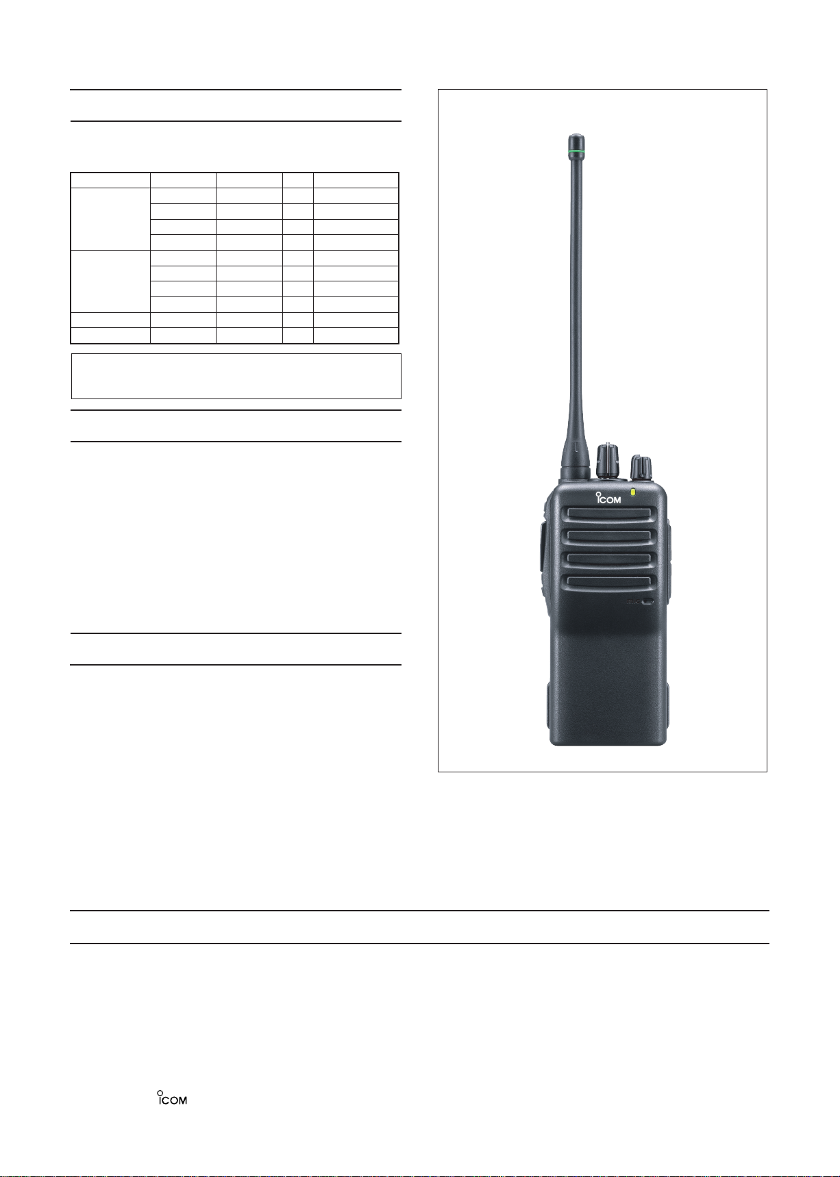
UHF TRANSCEIVERS
Page 2
INTRODUCTION
This s e r v i c e manual d e s c r i b e s t h e latest s e r v i c e
information for the
IC-F24/IC-F24S/IC-F25/IC-F25S UHF
TRANSCEIVER
at the time of publication.
DANGER
NEVER connect the transceiver to an AC outlet or to a DC
power supply that uses more than 8 V. Such a connection
could cause a fire or electric hazard.
DO NOT expose the transceiver to rain, snow or any liquids.
DO NOT reverse the polarities of the power supply when
connecting the transceiver.
DO NOT apply an RF signal of more than 20 dBm (100mW)
to the antenna connector. This could damage the transceiver's front end.
ORDERING PARTS
Be sure to include the following four points when ordering
replacement parts:
1. 10-digit order numbers
2. Component part number and name
3. Equipment model name and unit name
4. Quantity required
<SAMPLE ORDER>
2260002840 Switch SKHLLFA010 IC-F24 Main unit 5 pieces
8930063350 Lens 2775 Lens IC-F24 Chassis 10 pieces
Addresses are provided on the inside back cover for your
convenience.
1. Make sure the problem is internal before disassembling the transceiver.
2. DO NOT open the transceiver until the transceiver is disconnected from its power source.
3. DO NOT force any of the variable components. Turn them slowly and smoothly.
4. DO NOT short any circuits or electronic parts. An insulated turning tool MUST be used for all adjustments.
5. DO NOT keep power ON for a long time when the transceiver is defective.
6. DO NOT transmit power into a signal generator or a sweep generator.
7. ALWAYS connect a 30 dB to 40 dB attenuator between the transceiver and a deviation meter or spectrum analyzer when
using such test equipment.
8. READ the instructions of test equipment thoroughly before connecting equipment to the transceiver.
To upgrade quality, all electrical or mechanical parts and
internal circuits are subject to change without notice or
obligation.
Icom, Icom Inc. and are registered trademarks of Icom Incorporated (Japan) in the United States, the United Kingdom,
Germany, France, Spain, Russia and/or other countries.
MODEL VERSION SYMBOL CH FREQUENCY
IC–F24
USA–02 US2 16 400–470 MHz
USA–03 US3 16 450–512 MHz
GEN–02 GE2 16 450–470 MHz
GEN–03 GE3 16 450–520 MHz
IC–F24S
USA–02 US2S 2 400–470 MHz
USA–03 US3S 2 450–512 MHz
GEN–02 GE2 2 400–470 MHz
GEN–03 GE3 2 450–520 MHz
IC–F25 EUR–02 EU2 16 400–470 MHz
IC–F25S EUR–02 EU2S 2 400–470 MHz
REPAIR NOTES
Page 3

TABLE OF CONTENTS
SECTION 1 SPECIFICATIONS
SECTION 2 INSIDE VIEWS
SECTION 3 DISASSEMBLY INSTRUCTIONS
SECTION 4 CIRCUIT DESCRIPITON
4-1 RECEIVER CIRCUITS . . . . . . . . . . . . . . . . . . . . . . . . . . . . . . . . . . . . . . . . . . . . . . . . . . . . . . . 4-1
4-2 TRANSMITTER CIRCUITS . . . . . . . . . . . . . . . . . . . . . . . . . . . . . . . . . . . . . . . . . . . . . . . . . . . 4-2
4-3 PLL CIRCUITS . . . . . . . . . . . . . . . . . . . . . . . . . . . . . . . . . . . . . . . . . . . . . . . . . . . . . . . . . . . . . 4-3
4-4 OTHER CIRCUITS . . . . . . . . . . . . . . . . . . . . . . . . . . . . . . . . . . . . . . . . . . . . . . . . . . . . . . . . . . 4-4
4-5 POWER SUPPLY CIRCUITS . . . . . . . . . . . . . . . . . . . . . . . . . . . . . . . . . . . . . . . . . . . . . . . . . . 4-5
4-6 PORT ALLOCATIONS . . . . . . . . . . . . . . . . . . . . . . . . . . . . . . . . . . . . . . . . . . . . . . . . . . . . . . . 4-5
SECTION 5 ADJUSTMENT PROCEDURES
5-1 PREPARATION . . . . . . . . . . . . . . . . . . . . . . . . . . . . . . . . . . . . . . . . . . . . . . . . . . . . . . . . . . . . . 5-1
5-2 CONFIGURATION LISTS FOR ADJUSTMENTS . . . . . . . . . . . . . . . . . . . . . . . . . . . . . . . . . . . 5-2
5-3 SOFTWARE ADJUSTMENTS . . . . . . . . . . . . . . . . . . . . . . . . . . . . . . . . . . . . . . . . . . . . . . . . . 5-3
SECTION 6 PARTS LIST
SECTION 7 MECHANICAL PARTS AND DISASSEMBLY
SECTION 8 SEMI-CONDUCTOR INFORMATION
SECTION 9 BOARD LAYOUTS
9-1 MAIN UNIT . . . . . . . . . . . . . . . . . . . . . . . . . . . . . . . . . . . . . . . . . . . . . . . . . . . . . . . . . . . . . . . . 9-1
9-2 ANT UNIT . . . . . . . . . . . . . . . . . . . . . . . . . . . . . . . . . . . . . . . . . . . . . . . . . . . . . . . . . . . . . . . . . 9-1
9-3 CONNECT UNIT . . . . . . . . . . . . . . . . . . . . . . . . . . . . . . . . . . . . . . . . . . . . . . . . . . . . . . . . . . . . 9-1
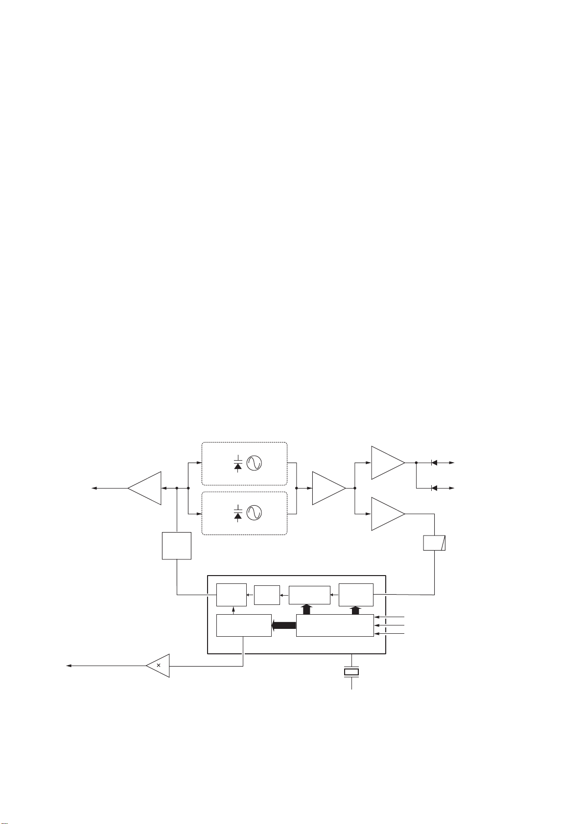
SECTION 10 BLOCK DIAGRAM
SECTION 11 VOLTAGE DIAGRAM
11-1 MAIN UNIT . . . . . . . . . . . . . . . . . . . . . . . . . . . . . . . . . . . . . . . . . . . . . . . . . . . . . . . . . . . . . . . . 11-1
Page 4
SECTION 1 SPECIFICATIONS
GENERAL
• Frequency coverage : 400–470 MHz [USA–02], [GEN–02], [EUR]
450–512 MHz [USA–03]
450–520 MHz [GEN–03]
• Type of emission :
• Number of conventional channels : 2 ch (IC-F24S/F25S), 16 ch (IC-F24/F25)
• Antenna impedance : 50 Ω (nominal)
• Operating temperature range : –30˚C to +60˚C (–22˚F to +140˚F) [USA], [GEN]
• Power supply requirement : 7.2 V DC nominal (negative ground)
• Current drain (at 7.2 V DC ; approx.) :
VERSION WIDE MIDDLE NARROW
[USA], [GEN]
[EUR]
–25˚C to +55˚C [EUR]
RECEIVING TRANSMITTING
Stand-by Max. audio
75 mA 300 mA 1.6 A 0.8 A
16K0F3E (25.0 kHz)
N/A
14K0F3E (20.0 kHz) 8K50F3E (12.5 kHz)
High (at 4 W) Low (at 1 W)
11K0F3E (12.5 kHz)
• Dimensions (projections not included) : 53(W)×120(H)×38(D) mm; 2
• Weight (Including BP-231) : Approximately 260 g (9
TRANSMITTER
• Output power (at 7.2 V DC) : 4 W
• Modulation : Variable reactance frequency modulation
• Maximum permissible deviation : ±5.0 kHz (Wide), ±4.0 kHz (Middle), ±2.5 kHz (Narrow)
• Frequency error : ±2.5 ppm
• Spurious emissions : 70 dB (min.) [USA], [GEN]
• Adjacent channel power : 70 dB min. (75 dB typical) for Wide
70 dB min. (73 dB typical) for Middle
60 dB min. (68 dB typical) for Narrow
• Audio harmonic distortion : 3% typical (1 kHz, 40% deviation)
• Hum and Noise ([USA], [GEN]) : 40 dB min. (46 dB typical) for Wide
• Residual modulation ([EUR] only) : 45 dB min. (55 dB typical) for Wide
(with CCITT filter) 43 dB min. (53 dB typical) for Middle
40 dB min. (50 dB typical) for Narrow
• Limiting charact of modulator : 60–100% of maximum deviation
• Microphone impedance : 2.2 k
• Receive system : Double conversion superheterodyne system
• Intermediate frequencies : 1st IF: 46.35 MHz, 2nd IF: 450 kHz
• Sensitivity : 0.25 µV (–119 dBm) typical at 12 dB SINAD [USA], [GEN]
• Squelch sensitivity (at threshold) : 0.25 µV typical [USA], [GEN]
• Adjacent channel selectivity : 70 dB min. (75 dB typical) for Wide
70 dB min. (73 dB typical) for Middle
60 dB min. (65 dB typical) for Narrow
• Spurious response : 70 dB min.
• Intermodulation rejection ratio : 70 dB min. (74 dB typical) [USA], [GEN]
• Hum and Noise ([USA], [GEN] only) : 40 dB min. (45 dB typical) for Wide
• Hum and Noise ([EUR] only) : 45 dB min. (55 dB typical) for Wide
• Audio output power : 0.5 W typical at 5% distortion with an 8 Ω load
• Output impedance (Audio) : 8
(without CCITT filter) 34 dB min. (40 dB typical) for Narrow
RECEIVER
(without CCITT filter) 34 dB min. (40 dB typical) for Narrow
(with CCITT filter) 43 dB min. (53 dB typical) for Middle
40 dB min. (50 dB typical) for Narrow
0.25 µW (≤1 GHz), 1.0 µW (>1 GHz) [EUR]
Ω
–4 dBµV (–111 dBm) emf typical at 20 dB SINAD
–4 dBµV emf typical [EUR]
65 dB min. (67 dB typical) [EUR]
Ω
3
⁄32(W)×423⁄32(H)×11⁄2(D) in
3
⁄16 oz)
[EUR]
Specifications are measured in accordance with EIA-152-C/204D, TIA-603 or EN 300 086.
All stated specifications are subject to change without notice or obligation.
1 - 1
Page 5
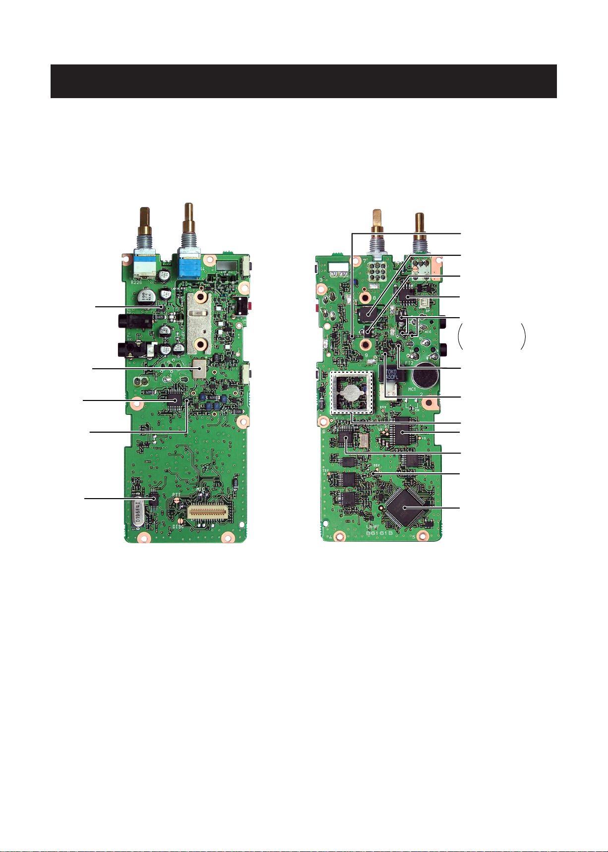
SECTION 2 INSIDE VIEWS
•
MAIN UNIT
2 - 1
+5 Regulator
(IC9: NJM2870)
AF amplifier
(IC12: TA7368F)
D/A converter
(IC8: M62363FP)
R5 Regulator
(Q22: 2SA1577)
CPU
(IC13: HD6433687A91FP)
S5 Regulator
Q23: 2SB1132
Q24: XP6501
Q25: UNR9113J
Crystal filter
(FI1: FL-335)
FM IF IC
(IC1: TA31136FN)
IF amplifier
(Q4: 2SC4215)
EEPROM
(IC15: BR24L16FV)
Power amplifier
(Q7: RD07MVS1)
T5 Regulator
(Q21: 2SA1577)
PLL IC
(IC4: MB15A02)
Pre-drive
(Q5: 2SC3356)
APC amplifier
(IC2: TC75S51F)
VCO circuit
TOP VIEW BOTTOM VIEW
Drive amplifier
(Q8: RD01MUS1)
Page 6
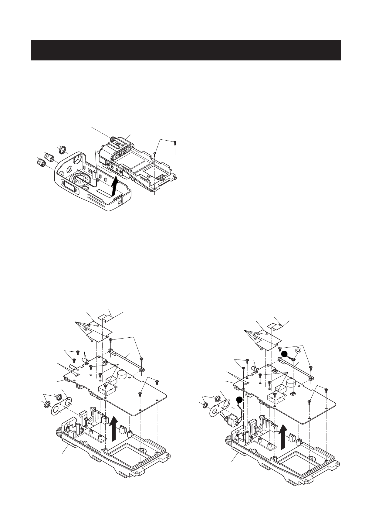
SECTION 3 DISASSEMBLY INSTRUCTIONS
3 - 1
Chassis unit
D
A
*B
C
E
*: IC-F24/F25 only
Shield cover
Earth plate
Main unit
K
M
M
N
M
F
G
Chassis unit
N
L
I
H
•
REMOVING THE CHASSIS UNIT
1 Unscrew 1 nut A, and remove 2 knobs *B, C.
2 Unscrew 2 screws D.
3 Take off the chassis unit in the direction of the arrow.
4 Unplug the connector E from the chassis unit.
•
REMOVING THE MAIN UNIT (IC-F24/F25)
1 Unscrew 2 nuts F, and remove the top plate G.
2 Unsolder 1 point H, and remove the earth plate.
3 Unsolder 5 points I, and remove the shield cover.
4 Unscrew 2 screws K, and remove the side plate L.
5 Unscrew 7 screws M.
6 Unsolder 4 points N, and take off the main unit in the
direction of the arrow.
Main unit
Chassis unit
Shield cover Earth plate
a
a
K
L
M
M
N
M
I
N
G
F
H
•
REMOVING THE MAIN UNIT (IC-F24S/F25S)
1 Remove the switch connector O.
2 Unsolder 2 nuts F, and remove the top plate G.
3 Unsolder 1 point H, and remove the earth plate.
4 Unsolder 5 points J, and remove the shield cover.
5 Unscrew 2 screws K, and remove the side plate L.
6 Unscrew 7 screws M.
7 Unsolder 4 points N, and take off the main unit in the
direction of the arrow.
Page 7
SECTION 4 CIRCUIT DESCRIPTION
4-1 RECEIVER CIRCUITS
4-1-1 ANTENNA SWITCHING CIRCUIT
The antenna switching circuit functions as a low-pass filter
while receiving and a resonator circuit while transmitting.
This circuit does not allow transmit signals to enter the
receiver circuits.
Received signals enter the antenna connector (CHASSIS;
J1) and pass through the low-pass filter (L1, L2, L45, C1–C6,
C175). The filtered signals are passed through the
antenna switching circuit (D2, D5, L5) and then applied to
the RF circuit.
4-1-2 RF CIRCUIT
The RF circuit amplifies signals within the range of frequency coverage and filters out-of-band signals.
The signals from the antenna switching circuit pass through
the bandpass filter (D3, D4, D7, D8, L7, L8, C21, C23,
C24). The filtered signals are amplified at the RF amplifier
(Q2) and then passed through the another bandpass filter
(D9, D10, C39, C40, C45) to suppress unwanted signals.
The filtered signals are applied to the 1st mixer circuit.
D3, D4, D7–D10 employ varactor diodes, that are controlled by the CPU via the D/A converter (IC8), to track
the bandpass filter. These varactor diodes tune the center
frequency of an RF passband for wide bandwidth receiving
and good image response rejection.
4-1-3 1ST MIXER AND 1ST IF CIRCUITS
The 1st mixer circuit converts the received signal into fixed
frequency of the 1st IF signal with the PLL output frequency. By changing the PLL frequency, only the desired
frequency passes through a crystal filter at the next stage
of the 1st mixer.
1
⁄
λ type
4
The RF signals from the bandpass filter are mixed with the
1st LO signals, where come from the RX VCO circuit via
the BPF (L12, L38, C49, C304, C305), at the 1st mixer circuit (Q3) to produce a 46.35 MHz 1st IF signal. The 1st IF
signal is passed through a monolithic filter (FI1) in order to
obtain selection capability and to pass only the desired signal. The filtered signal is applied to the 2nd IF circuit after
being amplified at the 1st IF amplifier (Q4).
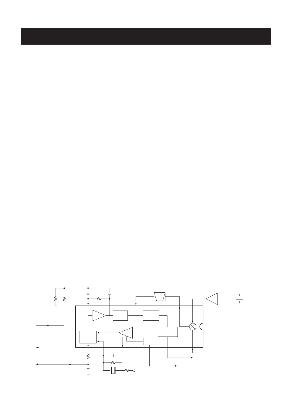
4-1-4 2ND IF AND DEMODULATOR CIRCUITS
The 2nd mixer circuit converts the 1st IF signal into a 2nd
IF signal. The double-conversion superheterodyne system
(which converts receive signals twice) improves the image
rejection ratio and obtains stable receiver gain.
The 1st IF signal from the IF amplifier (Q4) is applied to
the 2nd mixer section of the FM IF IC (IC1, pin 16), and
is mixed with the 2nd LO signal to be converted into a
450 kHz 2nd IF signal.
The FM IF IC (IC1) contains the 2nd mixer, 2nd local oscillator, limiter amplifier, quadrature detector, active filter and
noise amplifier circuits. The 2nd LO signal (45.9 MHz) is
produced at the PLL circuit by tripling it’s reference frequency (15.3 MHz).
The 2nd IF signal from the 2nd mixer (IC1, pin 3) passes
through the ceramic filter (FI2) to remove unwanted heterodyned frequencies. It is then amplified at the limiter
amplifier section (IC1, pin 5) and applied to the quadrature
detector section (IC1, pins 10, 11) to demodulate the 2nd
IF signal into AF signals.
The demodulated AF signals are output from pin 9 (IC1) as
“DET” signal, and are then applied to the AF circuit.
• 2ND IF AND DEMODULATOR CIRCUITS
87
Active
filter
"SQLC" signal from the
D/A converter IC
(IC8, pin 2)
To D/A converter IC
(IC8, pin 1)
AF signal "DET"
to the AF circuit
FM
detector
X1
Noise
AMP
Limiter
AMP
5
2nd IF filter
450 kHz
Noise
detector
RSSI
FI2
Noise
comparator
3
Mixer
45.9 MHz
2
Q19
×3
X2
15.3 MHz
IC1 TA31136FN
11109
12
"RSSI" signal to the CPU (IC13, pin 63)
R5V
13
"NOIS" signal to the CPU (IC13, pin 53)
16
1st IF signal from the IF amplifier (Q4)
4 - 1
Page 8
4-1-5 AF AMPLIFIER CIRCUIT
The AF amplifier circuit amplifies the demodulated AF signals to drive a speaker.
The AF signals from the FM IF IC (IC1, pin 9) pass through
the high-pass filter (IC6, pins 3 and 1) to suppress unwanted harmonic components. The signals pass through the
RX mute switch (Q34) which is controlled by “RMUT” signal from the CPU (IC13, pin 56), and are then applied to
another high-pass filter (IC6, pins 13 and 14). The filtered
signals pass through the low-pass filter (IC6, pins 6 and
7) via the analog switch (IC10, pins 1 and 2). The signals
are applied to the analog switch (IC10, pin 10) again, and
are then applied to the AF power amplifier (IC12, pin 4) via
the AF volume (R226). The amplified AF signals are output
from pin 10, and are then applied to the internal speaker
which is connected to J1 via the [SP] jack (J3).
4-1-6 RECEIVE MUTE CIRCUITS
• NOISE SQUELCH
A squelch circuit cuts out AF signals when no RF signals
are received. By detecting noise components in the AF signals, the squelch circuit switches the AF mute switch.
Some noise components in the AF signals from the FM IF
IC (IC1, pin 9) are applied to the D/A converter (IC8, pin
1) as “DET” signal, and are then output from pin 2. The
signals are applied to the active filter section in the FM IF
IC (IC1, pin 8). The active filter section filters and amplifies
noise components. The amplified signals are converted into
the pulse-type signals at the noise detector section and
output from pin 13 as “NOIS” signal.
The “NOIS” signal from the FM IF IC is applied to the CPU
(IC13, pin 53). Then the CPU analyzes the noise condition
and outputs the AF mute control signal from the CPU (pin
56) as “RMUT” signal from pin 56. The signal is applied to
the RX mute switch (Q34) to control the AF signal muting.
• CTCSS AND DTCS
The tone squelch circuit detects tone signals and opens the
squelch only when the receiving signal contains matched
subaudible tone (CTCSS or DTCS). When tone squelch is
in use, and a signal with a mismatched or no subaudible
tone is received, the tone squelch circuit mutes the AF signals even when noise squelch is open.
A portion of the “DET” signals from the FM IF IC (IC1, pin
9) passes through the low-pass filter (IC7, pins 5 and 7)
to remove AF (voice) signals, and are then applied to the
amplifier (IC7, pin 3). The amplified signals are applied to
the CTCSS or DTCS decoder inside of the CPU (IC13, pin
60) as the “CDEC” signal. The CPU outputs AF mute control signal from pin 56, and is then applied to the RX mute
switch (Q34) and analog switch (IC10, pins 12 and 13) to
control AF signals muting as “RMUT” signal.
4-2 TRANSMITTER CIRCUITS
4-2-1 MICROPHONE AMPLIFIER CIRCUIT
The microphone amplifier circuit amplifies audio signals
within +6 dB/octave pre-emphasis characteristics from the
microphone to a level needed for the modulation circuit.
The AF signals from the microphone are passed through
the microphone mute switch (Q35), and are then applied
to the amplifier (IC6, pins 9 and 8) via the high-pass filter
(IC6, pins 13 and 14). The amplified signals are applied to
the analog switch (IC10, pin 4), and outputs from pin 3. The
signals pass through the low-pass filter (IC6, pins 6 and 7),
then applied to the analog switch (IC10, pin 9) again and
output from pin 8.
The signals are applied to the D/A converter (IC8, pin 4).
The converted signals output from pin 3, and applied to the
modulation circuit (D18) as “MOD” signal.
• ANALOG SWITCHING CIRCUITS
"DET" AF signal
from FM IF IC (IC1, pin 9)
IC6 B
LPF
"CTCSS/DTCS" signal from
D/A conveter IC (IC8, pin 10)
"TONE" signal from CPU (IC13) via low-pass
filters (IC5 A / B pin 7)
2
3
9
10
8
IC8
D/A converter
IC6 A
HPF
Analog SW
(IC10)
MUTE
1
IC6 C
4
11
D18
FM mod.
Q34
RX
AMP
IC6 D
HPF
AF
volume
R226
to TX VCO circuit
(Q13, D17, D21)
IC12
AF
AMP
Q35
MIC
MUTE
Microphone
Speaker
4 - 2
Page 9
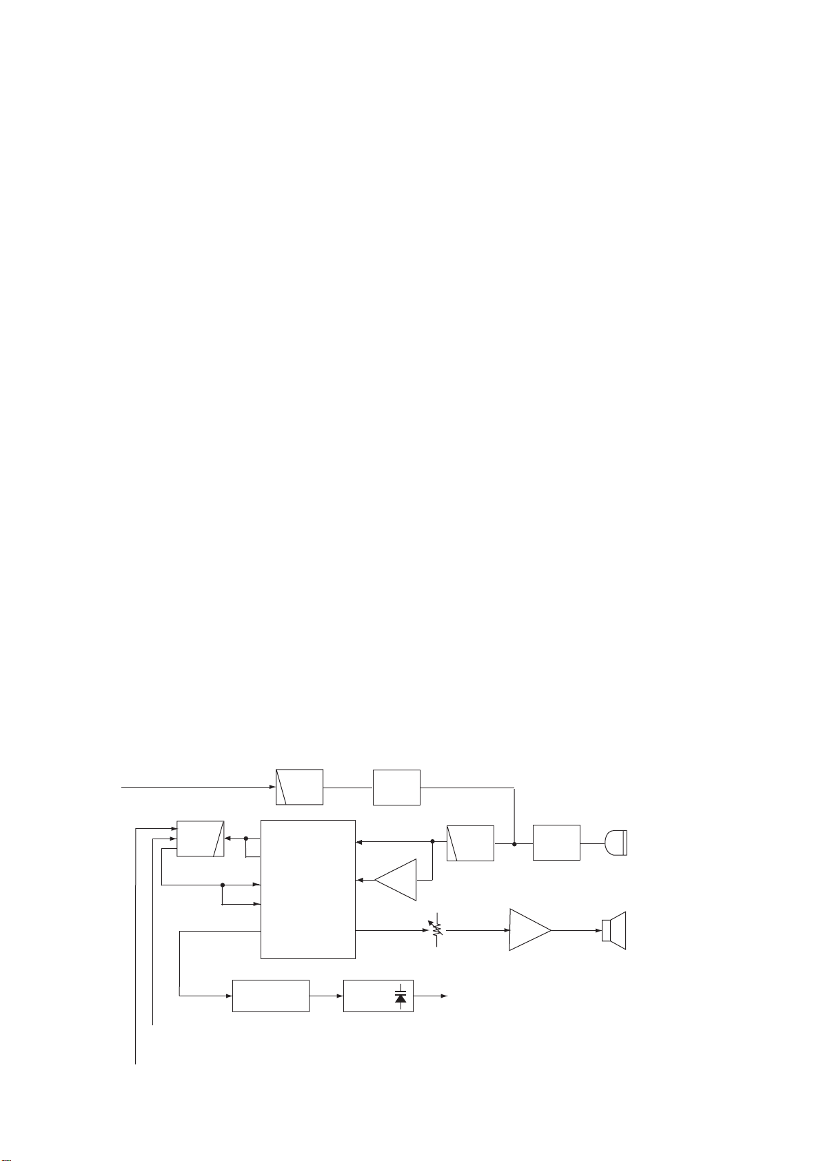
4-2-2 MODULATION CIRCUITS
The modulation circuit modulates the VCO oscillating signal
(RF signal) using the audio signals from the microphone.
4-2-4 APC CIRCUITS
The bias current of the drive (Q8) and power (Q7) amplifiers
are controlled by the APC circuit.
The AF signals from the D/A converter (IC8, pin 3) change
the reactance of varactor diode (D18) to modulate the oscillated signal at the TX VCO circuit (Q13, D17, D21). The
modulated VCO signal is amplified at the buffer amplifiers
(Q10, Q12) and then applied to the drive amplifier circuit via
the T/R switch (D14).
The CTCSS/DTCS signals (“CENC0,” “CENC1,” “CENC2”)
from the CPU (IC13, pins 23–25) pass through the low-pass
filter (IC5, pins 12 and 14) via 3 registers (R191–R193) to
change its waveform. Then the signals are applied to the
D/A converter (IC8, pin 9). The output signals from the D/A
converter (IC8, pin 10) pass through the low-pass filter
(IC6, pins 6 and 7) to be mixed with “MOD” signal, and then
applied to the D/A converter again (IC8, pin 4) after passing
through the analog switch (IC10, pins 8 and 9).
4-2-3 TRANSMIT AMPLIFIER CIRCUITS
Transmit amplifiers amplify the TX VCO oscillating signal to
transmit power level.
The modulated RF signal from the TX VCO circuit passes
through the T/R switch (D14) and is amplified at the YGR
(Q9), pre-drive (Q5), drive (Q8), and power (Q7) amplifiers
to obtain 4 W (max.) of RF power (at 7.2 V DC).
The amplified signal passes through the low-pass filter (L4,
C11, C13, C16), antenna switch (D2), the low-pass filter (L1
–L3, C2–C5, C175, C176) and power detector (D1, D30),
then applied to the antenna connector (CHASSIS unit; J1).
The APC circuit (IC2, D1, D30) protects drive and power
amplifiers from the reflected signal, and selects output
power of HIGH, LOW2 or LOW1.
The power detector (D1, D30) detects transmit output power
and converts it into DC voltage. The DC voltage is at a minimum level when the antenna impedance is matched to 50 Ω,
and increased when mismatched.
The detected voltage is applied to the differential amplifier
(IC2, pin 3), and the “T2” signal from the D/A converter (IC8,
pin 23), controlled by the CPU (IC13), is applied to pin 1 for
reference. When antenna impedance is mismatched, the
detected voltage exceeds the power setting voltage. Then
the output voltage of the differential amplifier (IC2, pin 4)
controls the input current of the drive (Q8), and power (Q7)
amplifiers to reduce the output power.
• APC CIRCUITS
VCC
T5V
RF signal
from Buffer AMP
T2
TMUT
YGR
AMP
Q9
+
IC2
APC
AMP
–
Q5
Pre-drive
AMP
Q8
Drive
AMP
Powe r
AMP
Q7
LPF
ANT
SW
D2, D5
D30 D1
LPF
to ANT
Power DET
4 - 3
Page 10
4-3 PLL CIRCUITS
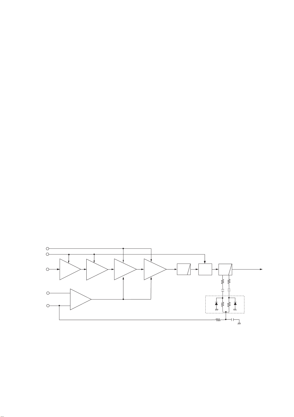
4-3-1 PLL CIRCUIT
A PLL circuit provides stable oscillation for the transmit frequency and the receive 1st LO frequency. The PLL output
compares the phase of the divided VCO frequency to the
reference frequency. The PLL output frequency is controlled
by the divided ratio (N-data) of a programmable divider.
The PLL circuit contains the TX/RX VCO circuits (TX:
Q13, D17, D18, D21; RX: Q14, D16, D22). The oscillated
signal is amplified at the buffer amplifiers (Q11, Q12) and
then applied to the PLL IC (IC4, pin 8) after being passed
through the low-pass filter (L32, C206, C208).
The PLL IC (IC4) contains a prescaler, programmable
counter, programmable divider and phase detector, charge
pump, etc. The entered signal is divided at the prescaler and
programmable counter section by the N-data ratio from the
CPU. The divided signal is detected on phase at the phase
detector using the reference frequency. The phase detected
signal is applied to the charge pump to be converted into
the DC voltage, and output from pin 5. After passes through
the loop filter (C130, C138, C146, C147, R95–R97), the DC
voltage is applied to the TX/RX VCO as the lock voltage.
If the oscillated signal drifts, its phase changes from that of
the reference frequency, causing a lock voltage change to
compensate for the drift in the oscillated frequency.
4-3-2 VCO CIRCUITS
The VCO circuit contains a separate RX VCO (Q14, D16,
D22) and TX VCO (Q13, D17, D21). The oscillated signal
is amplified at the buffer amplifiers (Q10, Q12) and is then
applied to the T/R switch (D14 for TX, D15 for RX). Then the
receive 1st LO (RX) signal is applied to the 1st mixer circuit
(Q3) and the transmit (TX) signal to the pre-drive amplifier
(Q9).
A portion of the signal from the buffer amplifier (Q12) is fed
back to the PLL IC (IC4, pin 8) via the buffer amplifier (Q11)
and low-pass filter (L32, C206, C208) as the comparison
signal.
• PLL CIRCUITS
"LVIN" signal to the CPU
(IC13, pin 64)
45.9 MHz 2nd LO
signal to the FM IF IC
(IC1, pin 2)
Buffer
Q18
Tripler
Q19
3
Loop
filter
Q14, D16, D22
Q13, D17, D21
Phase
5
detector
Programmable
divider
RX VCO
TX VCO
2
Charge
pump
Buffer
Q12
Programmable counter
Shift register
Buffer
Q10
Buffer
Q11
IC4 MB15A02
Prescaler
1
X2
15.3 MHz
8
10
11
9
CLOCK
DATA
PLST
D15
D14
LPF
to 1st mixer circuit
to transmitter circuit
4 - 4
Page 11

4-4 OTHER CIRCUITS
LED CONTROL CIRCUITS
The LED control circuit is composed of the CPU (IC13),
LED driver (Q32) and LED (DS1).
The CPU outputs “RLED” and “TLED” signals from the pins
42 and 43. The signals are applied to the LED driver (Q32,
pins 2 and 5). The driver outputs LED control signals to the
LEDs (DS1).
CONDITION COLOR
RECEIVING (2/5-TONE CODE) ORANGE
LOW BATTERY
(Nearly exhausted)
LOW BATTERY
(Almost exhausted)
CLONING ORANGE
RECEIVING/SQUELCH OPEN GREEN
TRANSMITTING RED
RED
RED
(Lighting)
(Blinks Slowly)
(Blinks Fast)
(Blinking)
(Lighting)
(Lighting)
4-5 POWER SUPPLY CIRCUIT
VOLTAGE LINE
LINE
VCC
+5V
S5V
R5V
T5V
The voltage from the connected battery pack.
Common 5 V converted from the VCC line at
the +5 regulator circuit (IC9). The output voltage
is supplied to the D/A converter (IC8), analog
SW (IC10), etc.
Common 5 V converted from the VCC line at
the S5 regulator circuit (Q23–Q25). The output
voltage is supplied to the ripple filter (Q17), PLL
IC (IC4), etc.
Receive 5 V converted from the S5V line at the
R5 regulator circuit (Q22). The output voltage
is supplied to the tripler (Q19), FM IF IC (IC1),
IF amplifier (Q4), VCO switch (Q15, Q16), 1st
mixer (Q3), etc.
Transmit 5 V converted from the S5V line at the
T5 regulator circuit (Q21). The output voltage is
supplied to the YGR (Q9), pre-drive (Q5), APC
amplifier (IC2), etc.
DESCRIPTION
4-6 PORT ALLOCATION
4-6-1 D/A CONVERTER IC (IC8)
Pin
number
11 BAL
14 LVA
15 REF
22 T1
23 T2
Port
name
Description
Outputs the modulation balance level
control signal. The signal is applied
to the reference frequency crystal
oscillator (X2, pin 1).
Outputs the PLL lock voltage control
signal. The output signal is applied to
the RX VCO (Q14, D16, D22) and TX
VCO (Q13, D17, D21).
Outputs the reference oscillator
correcting voltage. The voltage is applied
to
the reference frequency crystal
oscillator (X2, pin 1).
Outputs the bandpass filter tuning
signal. The output signal is applied to
the bandpass filters (D3, D4, D7, D8).
•
Outputs the bandpass filter tuning
signal during receive. The output
signal is applied to the bandpass
filters (D9, D10).
• Outputs the TX power control signal
during transmit. The output signal is
applied to the APC amplifier (IC2,
pin 1).
4 - 5
Page 12

4-6-2 CPU (IC13)
Pin
number
Port
name
1 TEMP
2BATV
7 RES
13 SENC0
14 SENC1
16 DUSE
18 AFON
19 SENC2
20 SENC3
21 CBI0
22 CBI1
23 CENC0
24 CENC1
25 CENC2
26 CBI2
27 CBI3
28 SCK
29 SO
30 BEEP
31 ESDA
32 ESCL
33 UNLK
34 PLST
36 NWC
37 DAST
38 S5C
39 T5C
40 R5C
Description
Input port for the transceiver’s
internal temperature detecting
signal.
Input port for the detect signal
for connecting battery pack’s
voltage.
Input port for power reset signal.
Output single tone encoder
signal.
Outputs DTSC LPF control
signal.
Outputs AF power amplifier
control signal.
Output single tone encoder
signal.
Input ports for rotary selector.
Output CTCSS/DTCS signals.
Input ports for rotary selector.
Outputs serial clock signal to
the PLL IC (IC4, pin 9), D/A
convertor (IC6, pin 7), etc.
Outputs serial data to the PLL IC
(IC6, pin 8) and D/A convertor
(IC6, pin 8).
Outputs beep audio signals.
I/O port for data signals from/to
the EEPROM (IC15, pin 5).
Outputs clock signal to the
EEPROM (IC15, pin 6).
Input port for unlock signal from
PLL IC.
Outputs strobe signals to the
PLL IC (IC4, pin 11).
Output/input port for wide/
narrow control signal.
• Outputs strobe signals to the
D/A convertor (IC8, pin 6).
• Input port for the connecting
battery type detect signal.
Outputs power save control
signal.
Outputs T5 regurator control
signal.
Low: While transmitting
Outputs R5 regurator control
signal.
Low: While receivinging
Pin
number
Port
name
Description
42 RLED Outputs receiving LED control signal.
43 TLED
Outputs transmitting LED control
signal.
44 OPT3
45 OPT1
I/O ports for option unit.
46 OPT2
Input port for the PTT switch detection
47 PTT
48 SI
49 CLI
50 CLO
53 NOIS
signal.
Low : While the PTT switch is pushed.
Serial Bus inputport.
Input port for the cloning data signal.
Outputs the cloning data signal.
Input port for the noise signal from the
FM IF IC (MAIN unit; IC1, pin 13).
54 CIRQ Input port for option unit detection.
55 CCS Outputs chip select signal.
56 TMUT Outputs transmit mute signal.
57 RMUT
Input port for AF mute signal from the
RX circuit.
58 MMUT Outputs MIC mute signal.
59 REMO Inputs key signal from remote mic.
60 CDEC
61 SDEC
Input port for CTCSS/DTCS signal
from the amplifier (IC5, pin 8).
Input port for single tone decode
signal from the LPF (IC5, pin 8).
62 KEY Inputs key input signal.
63 RSSI
64 LVIN
Input port for the S-meter signal from
the FM IF IC (IC1, pin 12).
Input port for the PLL lock voltage
.
4 - 6
6
Page 13

SECTION 5 ADJUSTMENT PROCEDURES
5-1 PREPARATION
When adjusting IC-F24/F25/S, the optional CS-F14 ADJ ADJUSTMENT SOFTWARE (Rev. 1.0 or later), JIG cable (see the illust
below) and OPC-478 (RS-232 type) or OPC-478U (USB type) CLONING CABLE are required.
REQUIRED TEST EQUIPMENTS
EQUIPMENT
DC power supply
FM deviation meter
Frequency counter
Digital multimeter
RF power meter
(terminated type)
SINAD meter
SYSTEM REQUIREMENTS
Output voltage : 7.2 V DC
Current capacity : 5 A or more
Frequency range : DC–600 MHz
Measuring range : 0 to ±10 kHz
Frequency range : 0.1–600 MHz
Frequency accuracy : ±1 ppm or better
Sensitivity : 100 mV or better
Input impedance : 10 MΩ/V DC or better
Measuring range : 1–10 W
Frequency range : 100–600 MHz
Impedance : 50
SWR : Less than 1.2 : 1
Measuring range : 20 –2 0 k H z
GRADE AND RANGE
Ω
• Microsoft® Windows® 98/SE/ME/2000/XP
• RS232C/USB port
BEFORE STARTING SOFTWARE ADJUSTMENT
Clone adjustment freqencies, TX power, CTCSS frequency,
DTCS code and IF bandwidth (see
ADJUSTMENT
CONFIGULATION on the next page) into the transceiver
using with the CS-F14
SOFTWARE ADJUSTMENTS. Otherwise, the transceiver
can not be adjusted.
CLONING SOFTWARE before starting
EQUIPMENT
Audio generator
Attenuator
Standard signal
generator (SSG)
Frequency range : 300–3000 Hz
Output level : 1–500 mV
Power attenuation : 20 or 30 dB
Capacity : 10 W or more
Frequency range : 100–600 MHz
Output level : 0.1 µV–32 mV
(As open circuit.)
DC voltmeter
Oscilloscope
AC millivoltmeter
STARTING SOFTWARE ADJUSTMENT
Input impedance : 50 kΩ/V DC or better
Frequency range : DC–20 MHz
Measuring range : 0.01–20 V
Measuring range : 10 mV–10 V
(1) Connect IC-F24/F25/S and PC with OPC-478/U
and JIG CABLE.
(2) Turn the transceiver power ON.
(3) Boot up Windows, and click the program group 'CS-F14 ADJ’
in the ‘Programs’ folder of the [Start] menu, then CS- F14
ADJ’s window appears.
(4) Click ‘Connect’ on the CS-F14’s window, then appears
IC-F14’s up-to-date condition.
(5) Set or modify adjustment data as desired.
GRADE AND RANGE
(–127 to –17 dBm)
CAUTION!: BACK UP the originally programmed memory
data in the transceiver before programming
the adjustment frequencies.
When program the adjustment frequencies
into the transceiver, the transceiver’s memory
data will be overwritten and lose original
memory data at the same time.
JIG CABLE
(
3-conductor 3.5(d) mm plug
JIG cable
To IC-F24/F25/S
[SP] jack
Microsoft and Windows are registered trademarks of
Microsoft Corporation in the U.S.A. and other countries.
( SP + )
(SP − )
(GND)
OPC-478/U
(CLONE)
5 - 1
Page 14

5-2 CONFIGULATION LIST FOR ADJUSTMENTS
- IC-F24/F25 -
[US2]=USA-02, [GE2]=GEN-02, [EU2]=EUR-02, [US3]=USA-03, [GE3]=GEN-03
FREQUENCY (MHz)
CH.
[US2], [EU2],
[GE2]
[US3], [GE3]
1 400.000 450.000
2 400.000 450.000
3 400.000 450.000
4 435.000 485.000
5 470.000 520.000
6 435.000 485.000
SETTING CONDITION CH.
Set TX power to High.
Set TX power to Low1.
Set TX power to Low2.
Set TX power to Low1.
Set TX power to Low1.
Set TX power to Low1.
Set DTCS code to 007.
Set IF bandwidth to Narrow.
7 435.000 485.000
8 435.000 485.000
9 435.000 485.000
10 435.000 485.000
11 400.000 450.000 Set IF bandwidth to Wide.
- IC-F24S/F25S -
• Re-clone these settings every time each category is adjusted. (1−8).
FREQUENCY (MHz)
[US2], [EU2],
[GE2]
[US3], [GE3]
SETTING CONDITION
Set TX power to Low1.
Set DTCS code to 007.
Set IF bandwidth to Wide/Middle.
(Middle : EUR only)
Set TX power to Low1.
Set IF bandwidth to Narrow.
Set TX power to Low1.
Set IF bandwidth to Wide/Middle.
(Middle : EUR only)
Set TX power to Low1.
Set IF bandwidth to Wide.
Set CTCSS to151.4Hz.
1.PLL LOCK VOLTAGE
2.REFERENCE FREQENCY
FREQUENCY (MHz)
CH.
[US2], [EU2],
[GE2]
[US3], [GE3]
1 400.000 450.000
2 470.000 520.000
3.TX POWER
FREQUENCY (MHz)
CH.
[US2], [EU2],
[GE2]
[US3], [GE3]
1 400.000 450.000
2 400.000 450.000
3 400.000 450.000
4.FM DEVIATION
FREQUENCY (MHz)
CH.
[US2], [EU2],
[GE2]
[US3], [GE3]
1 435.000 485.000
2 435.00 485.00
SETTING CONDITION
Set TX power to Low1.
Set TX power to Low1.
SETTING CONDITION
Set TX power to High.
Set TX power to Low2.
Set TX power to Low1.
SETTING CONDITION
Set TX power to Low1.
Set IF bandwidth to Narrow.
Set TX power to Low1.
Set IF bandwidth to Wide/Middle.
(Middle : [EUR] only)
5.MODULATION BALANCE
FREQUENCY (MHz)
CH.
[US2], [EU2],
[GE2]
[US3], [GE3]
SETTING CONDITION
Set TX power to Low1.
1 435.000 485.000
Set DTCS code to 007.
Set IF bandwidth to Narrow
Set TX power to Low1.
2 435.000 485.000
Set DTCS code to 007.
Set IF bandwidth to Wide/Middle
(Middle : [EUR] only)
6.CTCSS/DTCS DEVIATION
FREQUENCY (MHz)
CH.
[US2], [EU2],
[GE2]
[US3], [GE3]
SETTING CONDITION
Set TX power to Low1.
1 435.000 485.000
Set IF bandwidth to Wide.
Set CTCSS to 151.4Hz.
7.RX SENSITIVITY
8.SQUELCH LEVEL
FREQUENCY (MHz)
CH.
[US2], [EU2],
[GE2]
[US3], [GE3]
SETTING CONDITION
1 400.000 450.000 Set IF bandwidth to Wide
.
.
.
5 - 2
2
Page 15

CONNECTION
(
AC millivoltmeter
Standard signal generator
0.1 µV to 32 mV
(–127 dBm to –17 dBm)
DO NOT transmit while
an SSG is connected to
the antenna connector.
FM
deviation meter
Attenuator
20 dB / 30 dB
RF power meter
0.1–10 W/50 Ω
Frequency
counter
to the antenna connector
To [SP]
To [MIC]
OPC-478 (RS-232C type)
OPC-478U (USB type)
To [SP]
connector
JIG cable
(see page 5-1)
Audio generator
to RS-232C port
to USB port
PC
SINAD meter
Speaker (8 Ω)
JIG CABLE
(
To IC-F24/F25/S
[SP] jack
IC-F24/F25/S
3-conductor 3.5(d) mm plug
JIG cable
( SP + )
(SP − )
(GND)
OPC-478/U
(CLONE)
5 - 3
Page 16

PC SCREEN EXAMPLE
(
NOTE: The above screen is an example.
Each transceiver has its own specific values for each setting.
5 - 4
Page 17

5-3 SOFTWARE ADJUSTMENTS (TRANSMITTING)
Select the operation using [↑] / [↓] keys, then set specified value using [←] / [→] keys on the connected computer keyboard.
ADJUSTMENT ADJUSTMENT CONDITION
PLL LOCK
VOLTAGE
[LV (RX LVA)]
[LV (TX LVA)
1 • Operating CH : CH2 (*CH1)
• Receiving
2• Operating CH : CH2 (*CH1)
• Connect an RF power meter or 50
dummy load to the antenna connector.
• Transmitting
CONVENIENT:
PLL LOCK VOLTAGE can be adjusted automatically.
Select "TX LVA"/"TX LVA" item on the CS-F14 ADJ screen, and push [ENTER] key.
3 • Operating CH : CH5 (*CH2)
• Receiving
4• Operating CH : CH5 (*CH2)
• Connect an RF power meter or 50
dummy load to the antenna connector.
• Transmitting
REFERENCE
FREQUENCY
[REF]
OUTPUT
POWER
[Power (Hi)]
[Power (L2)] 2 • Operating CH : CH3 (*CH2)
[Power (L1)] • Operating CH : CH2 (*CH3)
FM
DEVIATION
[MOD N]
(Narrow)
[MOD Ratio]
(Middle; EUR only)
[MOD Ratio]
(Wide)
MODULATION
BALANCE
[BAL N]
(Narrow)
[BAL Ratio]
(Middle; EUR only)
[BAL Ratio]
(Wide)
1 • Operating CH : CH5 (*CH1)
• Transmitting
1 • Operating CH : CH1 (*CH1)
• Transmitting
• Transmitting
• Transmitting
1 • Operating CH : CH8 (*CH1)
• Set the deviation meter as:
HPF : OFF
LPF : 20 kHz
De-emphasis : OFF
Detector : (P_P)/2
• Connect the audio generator the [MIC]
connector and set as
: 1.0 kHz 150mV rms
• Transmitting
2 • Operating CH : CH9 (*CH2)
• Transmitting
3 • Operating CH : CH9 (*CH2)
• Transmitting
1 • Operating CH : CH6 (*CH1)
• No audio applied to the [MIC] input.
• Set the deviation meter as:
HPF : OFF
LPF : 20 kHz
De-emphasis : OFF
Detector : (P_P)/2
• Transmitting
2 • Operating CH : CH7 (*CH2)
• Transmitting
3 • Operating CH : CH7 (*CH2)
• Transmitting
Ω
Ω
UNIT
PC
screen
PC
screen
Top
panel
Top
panel
Top
panel
To p
panel
MEASUREMENT
LOCATION
"LVIN" item on the
CS-F14 ADJ's screen.
"LVIN" item on the
CS-F14 ADJ's screen.
Loosely couple the frequency
counter to the antenna
connector.
Connect the RF power meter
to the antenna connector.
Connect the FM deviation
meter to the antenna
connector through the
attenuator.
Connect the FM deviation
meter with the oscilloscope
to the antenna connector
through an attenuator.
VALU E
1.0 V
1.0 V
3.3–4.5 V
(Verify)
3.3–4.5 V
(Verify)
470.0000 MHz
[US2], [EU2], [GE2]
520.0000 MHz
[US3], [GE3]
4.0 W
2.0 W
1.0 W
±2.10 kHz
±3.20 kHz
±4.10 kHz
Set to square wave
form
*For F24S/F25S adjustment.
5 - 5
Page 18

5-3 SOFTWARE ADJUSTMENTS (RECEIVING)
• Select an operation using [↑] / [↓] keys, then set specified value using [←] / [→] keys on the connected computer keyboard.
ADJUSTMENT ADJUSTMENT CONDITION
CTCSS/DTCS
DEVIATION
[CTCS/DTCS]
RX
SENSITIVITY
[BPF T1],
[BPF T2]
1 • Operating CH : CH10 (*CH1)
• No audio applied to the [MIC] input.
• Transmitting
1 • Operating CH : CH11 (*CH1)
• Connect a standard signal generator to
the antenna connector and set as:
Frequency : 400.000 MHz
[US2], [EU2], [GE2]
450.000 MHz
[US3], [GE3]
Level : +20 dBµ (–87dBm)
Modulation : 1 kHz
Deviation : ±3.5 kHz
• Receiving
CONVENIENT:
RX SENSITIVITY can be adjusted automatically.
Select "BPF ALL" item on the CS-F14 ADJ's screen, and push [ENTER] key.
SQUELCH
LEVEL
[SQL]
1 • Operating CH : CH11 (*CH1)
•
Connect an SSG to the antenna connector
and set as:
Frequency : 400.000 MHz
[US2], [EU2], [GE2]
450.000 MHz
[US3], [GE3]
Level : –14 dBµ (–121dBm)
Modulation : 1 kHz
Deviation : ±3.5 kHz
• Receiving
UNIT
panel
Side
Panel
Side
pannel
MEASUREMENT
LOCATION
Top
Connect the FM deviation
meter to the antenna
connector through the
attenuator.
Connect the SINAD meter
with an 8 Ω load to the [SP]
jack through the JIG cable.
Connect a speaker to the
[SP] jack through the JIG
cable.
VALU E
±0.68 kHz
Minimum distortion level
Set “SQL level” to close
squelch.
Then set “SQL level”
point where the audio
signals just appears.
at the
*For F24S/F25S adjustment.
5 - 6
Page 19

SECTION 6 PARTS LIST
[MAIN UNIT]
REF ORDER
NO. NO.
IC1 1110003200 S.IC TA31136FN (EL) B 51.8/19
IC2 1130008560 S.IC TC75S51F (TE85L) T 68.9/21
IC4 1140005990 S.IC MB15A02PFV1-G-BND-ER T 38.3/35.7
IC5 1110005340 S.IC NJM12902V-TE1 T 29.7/11.6
IC6 1110005320 S.IC NJM13403V-TE1 T 15.9/34.6
IC7 1110005330 S.IC NJM12904V-TE1 T 29.2/34.6
IC8 1190000350 S.IC M62363FP-650C T 40.3/15.2
IC9 1110005350 S.IC NJM2870F05-TE1 B 84.2/14.2
IC10 1130011770 S.IC CD4066BPWR T 22.9/34.6
IC12 1110001810 S.IC TA7368F (ER) T 89.3/13.2
IC13 1140012260 S.IC HD64F3687FP [US2], [GE2] T 12.5/14.3
1140012350 S.IC HD6433687A91FP [Others]
IC14 1110006260 S.IC BD5242G-TR T 6.6/5.9
IC15 1130011540 S.IC BR24L16FV-WE2 B 16/11.6
Q1 1560000840 S.FET 2SK1829 (TE85R) T 75/39.6
Q2 1580000730 S.FET 3SK293 (TE85L) B 76.8/37.9
Q3 1580000760 S.FET 3SK299-T1 U73 B 66.2/37.9
Q4 1530002600 S.TR 2SC4215-O (TE85R) B 51.4/23.1
Q5 1530000371 S.TR 2SC3356-T1B S (R25) T 74.3/33.5
Q6 1590003230 S.TR UNR9113J-(TX) T 72.5/19.1
Q7 1560001230 S.FET RD07MVS1 T 82.6/27
Q8 1560001240 S.FET RD01MUS1 T 76.1/27.5
Q9 1530003310 S.TR 2SC5107-O (TE85R) T 67/30.3
Q10 1530003310 S.TR 2SC5107-O (TE85R) T 59.4/36.3
Q11 1530003310 S.TR 2SC5107-O (TE85R) B 56.3/37
Q12 1530003310 S.TR 2SC5107-O (TE85R) T 59/31.5
Q13 1530002920 S.TR 2SC4226-T1 R25 T 54.9/30.7
Q14 1530002920 S.TR 2SC4226-T1 R25 T 54.2/37.1
Q15 1590001400 S.TR XP1214 (TX) B 56.5/32.6
Q16 1590003290 S.TR UNR9213J-(TX) B 59.1/32.6
Q17 1530002850 S.TR 2SC4116-BL (TE85R) T 55.5/44.1
Q18 1560000540 S.FET 2SK880-Y (TE85R) B 51.5/40.4
Q19 1530002850 S.TR 2SC4116-BL (TE85R) T 43.3/29.9
Q21 1510000920 S.TR 2SA1577 T106 Q T 71.9/16.4
Q22 1510000920 S.TR 2SA1577 T106 Q T 24.9/25.9
Q23 1520000460 S.TR 2SB1132 T100 R T 81/15.2
Q24 1590001190 S.TR XP6501-(TX) .AB T 76.3/15.1
Q25 1590003230 S.TR UNR9113J-(TX) T 75.7/11.7
Q26 1590003290 S.TR UNR9213J-(TX) T 49.7/18.4
Q27 1590003290 S.TR UNR9213J-(TX) T 24.8/16.7
Q28 1590003430 S.TR UNR911HJ-(TX) B 63.1/10.6
Q29 1590003270 S.TR UNR9210J-(TX) B 35.7/9.2
Q30 1510001080 S.TR 2SA2048 TLR T 91.9/8.6
Q31 1590001190 S.TR XP6501-(TX) .AB T 91.4/5.2
Q32 1590003020 S.TR XP4216-(TX) T 16.5/23.1
Q33 1590003230 S.TR UNR9113J-(TX) T 19.9/22.5
Q34 1560001360 S.FET 2SK3019 TL T 10.7/30.1
Q35 1560001360 S.FET 2SK3019 TL T 9.1/26.6
D1 1750001080 S.DIO RB886G T2R B 90.2/38.7
D2 1750000580 S.DIO 1SV307 (TPH3) B 91.5/31.1
D3 1750000710 S.VCP HVC350BTRF B 87.5/33.5
D4 1750000710 S.VCP HVC350BTRF B 87.5/34.8
D5 1790001260 S.DIO MA2S077-(TX) B 87.4/36.7
D6 1790001240 S.DIO MA2S728-(TX) B 85/39.9
D7 1750000710 S.VCP HVC350BTRF B 81.8/33.5
D8 1750000710 S.VCP HVC350BTRF B 81.8/34.8
D9 1750000710 S.VCP HVC350BTRF B 73.6/35.9
D10 1750000710 S.VCP HVC350BTRF B 72.2/35.9
D14 1790001260 S.DIO MA2S077-(TX) T 65.8/35.3
D15 1790001260 S.DIO MA2S077-(TX) T 65.8/36.7
D16 1750000710 S.VCP HVC350BTRF T 52.6/38.9
D17 1750000710 S.VCP HVC350BTRF T 49.4/28.3
D18 1720000570 S.VCP MA368 (TX) B 49.6/26.9
D21 1750000710 S.VCP HVC350BTRF T 50.5/33.7
D22 1750000710 S.VCP HVC350BTRF T 50.5/35.2
D24 1790001250 S.DIO MA2S111-(TX) T 41.5/39.2
D25 1790001250 S.DIO MA2S111-(TX) T 70.5/40.4
D26 1790001790 S.DIO RB876W TL B 35.7/7.1
D27 1750000520 S.DIO DAN222TL B 21.3/6
D28 1790001260 S.DIO MA2S077-(TX) B 8.5/11.2
D29 1750000940 S.DIO ISS400 TE61 B 23.1/4
D30 1750001080 S.DIO RB886G T2R T 88.5/36.2
D31 1790001010 S.ZEN MA8043-L (TX) B 74.5/19.9
[US3], [GE3], [US3S], [GE3S] only
FI1 2030000150 S.MLH FL-335 (46.350 MHz) B 62.8/27.7
FI2 2020001840 CER ALFYM450F=K
FI3 2040001440 S.LC NFE31PT152Z1E9L B 81.2/17.8
[US2]=USA-02, [GE2]=GEN-02, [EU2]=EUR-02, [US3]=USA-03, [GE3]=GEN-03 S.=Surface mount
DESCRIPTION
M.
LOCATION
H/V
[MAIN UNIT]
REF ORDER
NO. NO.
X1 6070000190 S.DCR CDBCB450KCAY24-R0 T 54.4/20
X2 6050011940 S.XTL CR-783 (15.3 MHz) T 36.9/28.9
X3 6050011720 S.XTL CR-764 (19.6608 MHz) B 12/5.9
L1 6200008700 S.COL 0.30-0.9-6TR 17.5N B 94.7/36.4
L2 6200008240 S.COL 0.30-0.9-5TL 14N B 94.8/31.9
L3 6200009470 S.COL 0.40-0.9-2TL B 92.9/26.3
L4 6200009470 S.COL 0.40-0.9-2TL B 89.9/20.6
L5 6200009070 S.COL LQW18AN18NG00D B 89.1/36.5
[US3], [GE3], [US3S], [GE3S]
6200010850 S.COL LQW18AN22NG00D [Others]
L7 6200007690 S.COL LQW2BHN18NJ01L B 84.3/34.5
[US3], [GE3], [US3S], [GE3S]
6200007700 S.COL LQW2BHN22NJ01L [Others]
L8 6200007690 S.COL LQW2BHN18NJ01L B 78.9/35.3
[US3], [GE3], [US3S], [GE3S]
6200007700 S.COL LQW2BHN22NJ01L [Others]
L9 6200007670 S.COL LQW2BHN10NJ01L B 75.9/35.2
[US3], [GE3], [US3S], [GE3S]
6200007680 S.COL LQW2BHN12NJ01L [Others]
L11 6200007230 S.COL LQW2BHN15NJ01L B 70.6/37.8
[US2], [EU2], [GE2], [US2S], [EU2S], [GE2S]
6200007680 S.COL LQW2BHN12NJ01L [Others]
L12 6200005720 S.COL ELJRE 33NG-F B 63.5/38.8
[US2], [EU2], [GE2], [US2S], [EU2S], [GE2S]
6200005730 S.COL ELJRE 39NG-F [Others]
L13 6200003350 S.COL ELJNC R27K-F B 66.8/33.9
L15 6200002850 S.COL NL 252018T-R82J T 94.2/32.4
L17 6200008220 S.COL 0.40-1.4-5TR 21N B 81.2/20.9
L18 6200006770 S.COL ELJRE 1N5Z-F B 81.2/20.9
L19 6200005660 S.COL ELJRE 10NG-F T 76/35.5
[US3], [GE3], [US3S], [GE3S]
6200005670 S.COL ELJRE 12NG-F [Others]
L20 6200005680 S.COL ELJRE 15NG-F T 68.8/33.1
[US3], [GE3], [US3S], [GE3S]
6200005690 S.COL ELJRE 18NG-F [Others]
L21 6200007880 S.COL ELJRF 33NJF2 (33) T 59.2/38.6
L22 6200007900 S.COL ELJRF 22NJF2 (22) T 59.5/33.3
L23 6200002850 S.COL NL 252018T-R82J T 55.2/28.1
L25 6200008490 S.COL 0.30-0.9-3TR 7.5N T 49.5/29.9
L26 6200008510 S.COL 0.30-0.9-4TR 10.5N T 49/37.9
L27 6200004950 S.COL NL 252018T-1R8J B 52.8/29
L28 6200004950 S.COL NL 252018T-1R8J B 52/36.6
L29 6200004660 S.COL MLF1608A 1R8K-T T 43.9/36.4
L30 6200007880 S.COL ELJRF 33NJF2 (33) B 85.1/38.7
L32 6200007910 S.COL ELJRF 18NJF2 (18) B 55.9/42.3
L33 6200004480 S.COL MLF1608D R82K-T T 43.4/25.9
L35 6200003540 S.COL MLF1608D R22K-T T 41.7/31.8
L38 6200005710 S.COL ELJRE 27NG-F B 65.6/40.7
L40 6200002850 S.COL NL 252018T-R82J T 53.6/34.6
L41 6200007880 S.COL ELJRF 33NJF2 (33) B 58.4/38.2
L42 6200004950 S.COL NL 252018T-1R8J B 49.4/34
L43 6200004950 S.COL NL 252018T-1R8J B 49.4/31.1
L45 6200008700 S.COL 0.30-0.9-6TR 17.5N B 94.9/39.6
R1 7030003490 S.RES ERJ3GEYJ 272 V (2.7 kΩ) B 91.8/39.9
R2 7030005120 S.RES ERJ2GEJ 102 X (1 kΩ) B 92.1/37.7
R3 7030004970 S.RES ERJ2GEJ 470 X (47 Ω) T 66.7/22.7
[US2], [EU2], [GE2], [US2S], [EU2S], [GE2S]
7030005570 S.RES ERJ2GEJ 820 X (82 Ω) [Others]
R4 7030005050 S.RES ERJ2GEJ 103 X (10 kΩ) T 75.8/20.8
R5 7030005050 S.RES ERJ2GEJ 103 X (10 kΩ) T 73.3/21.1
[US2], [EU2], [GE2], [US2S], [EU2S], [GE2S]
7030005220 S.RES ERJ2GEJ 223 X (22 kΩ) [Others]
R6 7030005090 S.RES ERJ2GEJ 104 X (100 kΩ) T 66.7/18.2
R7 7030005310 S.RES ERJ2GEJ 124 X (120 kΩ) T 68/17.7
R8 7030005100 S.RES ERJ2GEJ 154 X (150 kΩ) T 71.3/21.1
[US3], [GE3], [US3S], [GE3S]
7030005170 S.RES ERJ2GEJ 474 X (470 kΩ) [Others]
R9 7030008280 S.RES ERJ2GEJ 271 X (270 Ω) T 71.3/22.4
R10 7030005120 S.RES ERJ2GEJ 102 X (1 kΩ) T 68.4/24
R11 7030005090 S.RES ERJ2GEJ 104 X (100 kΩ) T 85.5/36.7
R12 7030005530 S.RES ERJ2GEJ 100 X (10 Ω) T 77.5/37.5
R13 7030005090 S.RES ERJ2GEJ 104 X (100 kΩ) T 82.3/35.7
R14 7030005050 S.RES ERJ2GEJ 103 X (10 kΩ) T 83.9/36.7
R15 7030005240 S.RES ERJ2GEJ 473 X (47 kΩ) B 79.1/39
R16 7030004980 S.RES ERJ2GEJ 101 X (100 Ω) B 74.8/39.9
R17 7030004970 S.RES ERJ2GEJ 470 X (47 Ω) B 74/33.3
R18 7030005050 S.RES ERJ2GEJ 103 X (10 kΩ) T 78.8/36.7
R19 7030005080 S.RES ERJ2GEJ 823 X (82 kΩ) T 78.8/38.7
R20 7030005120 S.RES ERJ2GEJ 102 X (1 kΩ) B 75.9/33.7
[US2], [EU2], [GE2], [US2S], [EU2S], [GE2S]
7030005240 S.RES ERJ2GEJ 473 X (47 kΩ) [Others]
DESCRIPTION
M.=Mounted side (T: Mounted on the Top side, B: Mounted on the Bottom side)
M.
LOCATION
H/V
6 - 1
Page 20

[MAIN UNIT]
REF ORDER
NO. NO.
R21 7030005110 S.RES ERJ2GEJ 224 X (220 kΩ) T 72.2/38.9
R22 7030005050 S.RES ERJ2GEJ 103 X (10 kΩ) T 69.2/38.9
R23 7030005110 S.RES ERJ2GEJ 224 X (220 kΩ) T 71.2/38.9
R24 7030005050 S.RES ERJ2GEJ 103 X (10 kΩ) T 64.6/38
R25 7030005040 S.RES ERJ2GEJ 472 X (4.7 kΩ) B 68/37.8
R29 7030007270 S.RES ERJ2GEJ 151 X (150 Ω) B 64.2/35.1
R30 7030005120 S.RES ERJ2GEJ 102 X (1 kΩ) B 67.7/35.7
R31 7030004980 S.RES ERJ2GEJ 101 X (100 Ω) B 64.2/34.1
R32 7030004980 S.RES ERJ2GEJ 101 X (100 Ω) B 66.1/31.1
R33 7030007270 S.RES ERJ2GEJ 151 X (150 Ω) B 55.5/25.2
R34 7030005110 S.RES ERJ2GEJ 224 X (220 kΩ) B 52.5/25.2
R35 7030004980 S.RES ERJ2GEJ 101 X (100 Ω) B 50.5/25.2
R36 7030007300 S.RES ERJ2GEJ 332 X (3.3 kΩ) T 52.5/15.5
R37 7030009140 S.RES ERJ2GEJ 272 X (2.7 kΩ) T 50.7/16.3
R38 7030005090 S.RES ERJ2GEJ 104 X (100 kΩ) T 46.5/21
R39 7030004970 S.RES ERJ2GEJ 470 X (47 Ω) B 55.8/22.3
R40 7030007270 S.RES ERJ2GEJ 151 X (150 Ω) B 56.2/21.1
R43 7030004970 S.RES ERJ2GEJ 470 X (47 Ω) B 47.5/15.4
R44 7030005090 S.RES ERJ2GEJ 104 X (100 kΩ) B 54.8/15.4
R45 7030005070 S.RES ERJ2GEJ 683 X (68 kΩ) B 52.8/13.7
R46 7030005000 S.RES ERJ2GEJ 471 X (470 Ω) B 53.8/13.7
R48 7030005000 S.RES ERJ2GEJ 471 X (470 Ω) B 51.5/25.2
R50 7030004980 S.RES ERJ2GEJ 101 X (100 Ω) T 66.3/38
R51 7030003670 S.RES ERJ3GEYJ 823 V (82 kΩ) B 96.5/37.3
R52 7030004990 S.RES ERJ2GEJ 221 X (220 Ω) T 93.3/35.9
R53 7030004970 S.RES ERJ2GEJ 470 X (47 Ω) T 80/22.5
R53 7030005530 S.RES ERJ2GEJ 100 X (10 Ω) T 80/22.5
[US2], [EU2], [GE2], [US2S], [EU2S], [GE2S]
7030005710 S.RES ERJ2GEJ 121 X (120 Ω) [Others]
R54 7030005060 S.RES ERJ2GEJ 333 X (33 kΩ) T 81.3/21.4
R55 7030005040 S.RES ERJ2GEJ 472 X (4.7 kΩ) T 80/20.9
R56 7030003860 S.RES ERJ3GE JPW V T 78/22.4
R57 7030004970 S.RES ERJ2GEJ 470 X (47 Ω) T 75.2/23.2
R58 7030005060 S.RES ERJ2GEJ 333 X (33 kΩ) T 72.1/24
[US3], [GE3], [US3S], [GE3S] only
R59 7030005040 S.RES ERJ2GEJ 472 X (4.7 kΩ) T 71.2/24
R61 7030004970 S.RES ERJ2GEJ 470 X (47 Ω) T 71.8/36.3
R62 7030005220 S.RES ERJ2GEJ 223 X (22 kΩ) T 72.1/35
R65 7030004980 S.RES ERJ2GEJ 101 X (100 Ω) T 69.4/34.2
R66 7030007340 S.RES ERJ2GEJ 153 X (15 kΩ) T 67.8/34.2
R67 7030004980 S.RES ERJ2GEJ 101 X (100 Ω) T 67.8/35.1
R68 7030005050 S.RES ERJ2GEJ 103 X (10 kΩ) T 69.4/35.1
R69 7030005040 S.RES ERJ2GEJ 472 X (4.7 kΩ) T 64.1/35.2
R70 7030005530 S.RES ERJ2GEJ 100 X (10 Ω) B 57.6/40.3
R71 7030005070 S.RES ERJ2GEJ 683 X (68 kΩ) T 58.2/38.6
R73 7030004980 S.RES ERJ2GEJ 101 X (100 Ω) B 57.7/30.5
R75 7030005110 S.RES ERJ2GEJ 224 X (220 kΩ) B 58.4/36.1
R76 7030004980 S.RES ERJ2GEJ 101 X (100 Ω) B 57.6/39.3
R77 7030005050 S.RES ERJ2GEJ 103 X (10 kΩ) B 56.7/30.5
R78 7030005090 S.RES ERJ2GEJ 104 X (100 kΩ) T 57.8/33.3
R79 7030006020 S.RES RR0510P-682-D (6.8 kΩ) T 56.5/39.1
R80 7030005120 S.RES ERJ2GEJ 102 X (1 kΩ) B 54.6/32.8
[US3], [GE3], [US3S], [GE3S]
7030008370 S.RES ERJ2GEJ 561 X (560 Ω) [Others]
R82 7030009320 S.RES ERJ2GEJ 4R7 X (4.7 Ω) T 52.6/32
R83 7030006020 S.RES RR0510P-682-D (6.8 kΩ) T 54.1/32.6
R84 7030006020 S.RES RR0510P-682-D (6.8 kΩ) T 52.1/28.6
R85 7030006020 S.RES RR0510P-682-D (6.8 kΩ) T 54.7/39.1
R86 7030005530 S.RES ERJ2GEJ 100 X (10 Ω) B 48.2/28.8
R87 7030005110 S.RES ERJ2GEJ 224 X (220 kΩ) B 48.1/25.3
R88 7030005010 S.RES ERJ2GEJ 681 X (680 Ω) B 54.6/31
[US3], [GE3], [US3S], [GE3S]
7030008370 S.RES ERJ2GEJ 561 X (560 Ω) [Others]
R89 7030005050 S.RES ERJ2GEJ 103 X (10 kΩ) B 49.3/41.2
R90 7030005170 S.RES ERJ2GEJ 474 X (470 kΩ) B 46.9/25.1
R92 7030005310 S.RES ERJ2GEJ 124 X (120 kΩ) B 46.9/26.1
R93 7030005120 S.RES ERJ2GEJ 102 X (1 kΩ) T 39.8/39.4
R94 7030005100 S.RES ERJ2GEJ 154 X (150 kΩ) T 41.8/40.8
R95 7030005120 S.RES ERJ2GEJ 102 X (1 kΩ) B 49.9/36.4
R96 7030008410 S.RES ERJ2GEJ 392 X (3.9 kΩ) B 49.3/40.1
[US2], [EU2], [GE2], [US2S], [EU2S], [GE2S]
7030009140 S.RES ERJ2GEJ 272 X (2.7 kΩ) [Others]
R97 7030005120 S.RES ERJ2GEJ 102 X (1 k
R98 7030007290 S.RES ERJ2GEJ 222 X (2.2 kΩ) T 53.5/44.1
R100 7030005040 S.RES ERJ2GEJ 472 X (4.7 kΩ) B 52.9/38.8
R101 7030005000 S.RES ERJ2GEJ 471 X (470 Ω) B 51.4/43.3
R103 7030005240 S.RES ERJ2GEJ 473 X (47 kΩ) T 33.1/27.8
R104 7030005230 S.RES ERJ2GEJ 334 X (330 kΩ) T 31.5/26.9
R105 7030005170 S.RES ERJ2GEJ 474 X (470 kΩ) T 32.6/29.1
R106 7030005050 S.RES ERJ2GEJ 103 X (10 kΩ) T 37.5/32
R107 7030005580 S.RES ERJ2GEJ 560 X (56 Ω) B 55.9/43.3
R108 7030005600 S.RES ERJ2GEJ 273 X (27 kΩ) T 44.9/21
[US2], [EU2], [GE2], [US2S], [EU2S], [GE2S]
7030008290 S.RES ERJ2GEJ 183 X (18 kΩ) [Others]
R109 7030005090 S.RES ERJ2GEJ 104 X (100 kΩ) T 43.9/21
R110 7030005240 S.RES ERJ2GEJ 473 X (47 kΩ) B 21.8/34.3
R111 7030005090 S.RES ERJ2GEJ 104 X (100 kΩ) T 27.1/28.7
R113 7030006610 S.RES ERJ2GEJ 394 X (390 kΩ) B 46.9/31.1
R114 7030005100 S.RES ERJ2GEJ 154 X (150 kΩ) B 46.9/29.1
R115 7030007570 S.RES ERJ2GEJ 122 X (1.2 kΩ) T 40.5/32
R116 7030007060 S.RES ERJ2GEJ 684X (680 kΩ) T 43.4/32.7
R117 7030005040 S.RES ERJ2GEJ 472 X (4.7 kΩ) T 35.3/40.1
R118 7030005040 S.RES ERJ2GEJ 472 X (4.7 kΩ) T 37.2/40.1
[US2S]=F24S USA-02, [GE2S]=F24S GEN-02, [EU2S]=F25S EUR-02
[US3S]=F24S USA-03, [GE3S]=F24S GEN-03
DESCRIPTION
) B 49.3/38.1
Ω
S.=Surface mount
M.
LOCATION
H/V
[MAIN UNIT]
REF ORDER
NO. NO.
R123 7030008400 S.RES ERJ2GEJ 182 X (1.8 kΩ) T 75.2/37.7
R124 7030005170 S.RES ERJ2GEJ 474 X (470 kΩ) T 72.7/40.4
R125 7030005110 S.RES ERJ2GEJ 224 X (220 kΩ) T 73.2/38.9
R131 7510001730 S.TMR ERTJOEP 473J T 40.9/28.1
R132 7030010080 S.RES ERJ2RHD 104 X (100 kΩ) T 40.9/27.1
R133 7030005050 S.RES ERJ2GEJ 103 X (10 kΩ) T 84.1/14.2
R134 7030005040 S.RES ERJ2GEJ 472 X (4.7 kΩ) T 74/14.3
R135 7030005050 S.RES ERJ2GEJ 103 X (10 kΩ) T 24.5/24
R136 7030005040 S.RES ERJ2GEJ 472 X (4.7 kΩ) T 22.8/24
R137 7030005050 S.RES ERJ2GEJ 103 X (10 kΩ) T 69.8/14.7
R138 7030005040 S.RES ERJ2GEJ 472 X (4.7 kΩ) T 69.8/16.7
R141 7030005000 S.RES ERJ2GEJ 471 X (470 Ω) T 37/9.9
R142 7030005000 S.RES ERJ2GEJ 471 X (470 Ω) T 43/9.9
R143 7030007340 S.RES ERJ2GEJ 153 X (15 kΩ) T 37.2/24.4
R144 7030005050 S.RES ERJ2GEJ 103 X (10 kΩ) B 46.5/13.7
R145 7030005090 S.RES ERJ2GEJ 104 X (100 k
R146 7030005090 S.RES ERJ2GEJ 104 X (100 kΩ) T 31.6/18.1
R147 7030007350 S.RES ERJ2GEJ 393 X (39 kΩ) T 33.4/16.1
R148 7030005080 S.RES ERJ2GEJ 823 X (82 kΩ) T 31.6/16.1
R149 7030006610 S.RES ERJ2GEJ 394 X (390 kΩ) T 33.4/12.9
R150 7030008300 S.RES ERJ2GEJ 184 X (180 kΩ) T 33.4/11.9
R151 7030005030 S.RES ERJ2GEJ 152 X (1.5 kΩ) T 33.4/13.9
R152 7030005220 S.RES ERJ2GEJ 223 X (22 kΩ) T 31.1/29.6
R153 7030005220 S.RES ERJ2GEJ 223 X (22 kΩ) T 29.9/29.1
R154 7030005220 S.RES ERJ2GEJ 223 X (22 kΩ) T 28.2/30.1
R155 7030005090 S.RES ERJ2GEJ 104 X (100 kΩ) T 29.8/41.1
R156 7030005170 S.RES ERJ2GEJ 474 X (470 kΩ) T 29.8/40.1
R157 7030007290 S.RES ERJ2GEJ 222 X (2.2 kΩ) T 31.5/39.1
R159 7030008010 S.RES ERJ2GEJ 123 X (12 kΩ) T 15.7/28.8
R160 7030004980 S.RES ERJ2GEJ 101 X (100 Ω) B 5.5/31
R161 7030005040 S.RES ERJ2GEJ 472 X (4.7 kΩ) T 12.9/27.3
R162 7030005050 S.RES ERJ2GEJ 103 X (10 kΩ) T 8.7/29.1
R163 7030005050 S.RES ERJ2GEJ 103 X (10 kΩ) T 14.1/29.8
R164 7030008410 S.RES ERJ2GEJ 392 X (3.9 kΩ) T 15.7/27.8
R165 7030008410 S.RES ERJ2GEJ 392 X (3.9 kΩ) T 12.6/31.9
R166 7030005240 S.RES ERJ2GEJ 473 X (47 kΩ) T 12.6/36.1
R167 7030009290 S.RES ERJ2GEJ 562 X (5.6 kΩ) T 15.7/29.8
R168 7030005000 S.RES ERJ2GEJ 471 X (470 Ω) T 16.3/40.1
R169 7030005100 S.RES ERJ2GEJ 154 X (150 kΩ) T 18/41.1
R170 7030008010 S.RES ERJ2GEJ 123 X (12 kΩ) T 12.9/29.3
R171 7030005100 S.RES ERJ2GEJ 154 X (150 kΩ) T 11.6/36.1
R172 7030005700 S.RES ERJ2GEJ 274 X (270 kΩ) T 18/39.1
R173 7030005310 S.RES ERJ2GEJ 124 X (120 kΩ) T 19.4/26.8
R174 7030005090 S.RES ERJ2GEJ 104 X (100 kΩ) T 19.4/28.8
R175 7030005110 S.RES ERJ2GEJ 224 X (220 kΩ) T 19.4/27.8
R176 7030005100 S.RES ERJ2GEJ 154 X (150 kΩ) T 17.7/27.8
R177 7030005060 S.RES ERJ2GEJ 333 X (33 kΩ) T 17.7/28.8
R178 7030005710 S.RES ERJ2GEJ 121 X (120 Ω) T 19.4/30.7
R179 7030005120 S.RES ERJ2GEJ 102 X (1 kΩ) B 11.5/16.8
R180 7030005160 S.RES ERJ2GEJ 105 X (1 MΩ) T 24.7/40.1
R181 7030005240 S.RES ERJ2GEJ 473 X (47 kΩ) T 21.1/40.1
R182 7030005090 S.RES ERJ2GEJ 104 X (100 kΩ) T 24.7/39.1
R183 7030006020 S.RES RR0510P-682-D (6.8 kΩ) B 17.2/39.1
R184 7030008250 S.RES RR0510P-562-D (5.6 kΩ) B 17.7/40.4
R185 7030005310 S.RES ERJ2GEJ 124 X (120 kΩ) B 18.7/40.4
R186 7030005080 S.RES ERJ2GEJ 823 X (82 kΩ) T 19.4/29.8
R187 7030005120 S.RES ERJ2GEJ 102 X (1 kΩ) B 9/18.2
R190 7030007280 S.RES ERJ2GEJ 331 X (330 Ω) T 34.7/18.9
R191 7030008300 S.RES ERJ2GEJ 184 X (180 kΩ) T 18/4.1
R192 7030005720 S.RES ERJ2GEJ 563 X (56 kΩ) T 18/5.1
R193 7030005220 S.RES ERJ2GEJ 223 X (22 kΩ) T 18/6.1
R194 7030005220 S.RES ERJ2GEJ 223 X (22 kΩ) T 23.9/10.9
R195 7030005050 S.RES ERJ2GEJ 103 X (10 kΩ) T 19.7/4.1
R196 7030005240 S.RES ERJ2GEJ 473 X (47 kΩ) T 23.9/11.9
R197 7030005240 S.RES ERJ2GEJ 473 X (47 kΩ) T 23.9/12.9
R198 7030005240 S.RES ERJ2GEJ 473 X (47 kΩ) T 25.7/12.9
R200 7030005040 S.RES ERJ2GEJ 472 X (4.7 kΩ) T 25.7/14.9
R201 7030005240 S.RES ERJ2GEJ 473 X (47 kΩ) T 23.9/14.9
R206 7030005110 S.RES ERJ2GEJ 224 X (220 kΩ) T 13.4/4.1
R207 7030005090 S.RES ERJ2GEJ 104 X (100 kΩ) T 13.4/5.1
R208 7030005240 S.RES ERJ2GEJ 473 X (47 kΩ) T 15.6/5.1
R209 7030005220 S.RES ERJ2GEJ 223 X (22 kΩ) T 15.6/6.1
R210 7030008010 S.RES ERJ2GEJ 123 X (12 kΩ) T 15.6/4.1
R211 7030005070 S.RES ERJ2GEJ 683 X (68 kΩ) T 27.1/4.1
R212 7030005070 S.RES ERJ2GEJ 683 X (68 kΩ) T 27.1/5.1
R213 7030005070 S.RES ERJ2GEJ 683 X (68 kΩ) T 27.1/6.1
R214 7030005070 S.RES ERJ2GEJ 683 X (68 kΩ) T 29.1/7.1
R215 7030005070 S.RES ERJ2GEJ 683 X (68 kΩ) T 31/6.1
R220 7030004980 S.RES ERJ2GEJ 101 X (100 Ω) B 15.9/23.3
R221 7030005000 S.RES ERJ2GEJ 471 X (470 Ω) B 66.5/13.7
R222 7030005080 S.RES ERJ2GEJ 823 X (82 kΩ) B 63.9/8.5
R223 7030005060 S.RES ERJ2GEJ 333 X (33 kΩ) B 61/11.3
R224 7030005000 S.RES ERJ2GEJ 471 X (470
R225 7030004980 S.RES ERJ2GEJ 101 X (100 Ω) B 33.9/7.1
R226 7210003061 VAR TP76N00N-15F-A103-2251A
R227 7030005050 S.RES ERJ2GEJ 103 X (10 kΩ) T 94.9/13.9
R228 7030005120 S.RES ERJ2GEJ 102 X (1 kΩ) T 94.2/15.2
R229 7030005530 S.RES ERJ2GEJ 100 X (10 Ω) T 86/9.7
R230 7030005530 S.RES ERJ2GEJ 100 X (10 Ω) T 87.2/17.2
R231 7030005120 S.RES ERJ2GEJ 102 X (1 kΩ) T 90.6/2.8
R232 7030007300 S.RES ERJ2GEJ 332 X (3.3 kΩ) T 93.2/4.4
R233 7030007300 S.RES ERJ2GEJ 332 X (3.3 kΩ) T 92.7/2.8
R234 7030005100 S.RES ERJ2GEJ 154 X (150 kΩ) B 23.3/6.2
DESCRIPTION
) T 33.4/18.1
Ω
) B 75.5/10.3
Ω
M.=Mounted side (T: Mounted on the Top side, B: Mounted on the Bottom side)
M.
LOCATION
H/V
6 - 2
Page 21

[MAIN UNIT]
REF ORDER
NO. NO.
R235 7030005090 S.RES ERJ2GEJ 104 X (100 kΩ) B 20.3/4.2
R236 7030005230 S.RES ERJ2GEJ 334 X (330 kΩ) B 23.3/5.2
R237 7030005050 S.RES ERJ2GEJ 103 X (10 kΩ) T 21.1/39.1
R238 7410001140 S.ARY EXB28V104JX B 40.9/9.5
R240 7030005590 S.RES ERJ2GEJ 680 X (68 Ω) T 99.7/12.3
R241 7030010040 S.RES ERJ2GE-JPW T 39.4/6.4
[US2S], [US3S], [EU2S], [GE2S], [GE3S] only
R242 7030010040 S.RES ERJ2GE-JPW T 41.4/6.4
[US2S], [US3S], [EU2S], [GE2S], [GE3S] only
R251 7030008010 S.RES ERJ2GEJ 123 X (12 kΩ) B 5.9/9.1
R252 7030005530 S.RES ERJ2GEJ 100 X (10 Ω) B 13.7/9.1
R254 7030008010 S.RES ERJ2GEJ 123 X (12 kΩ) B 9.3/10.1
R255 7030008010 S.RES ERJ2GEJ 123 X (12 kΩ) B 7.6/10.1
R256 7030005050 S.RES ERJ2GEJ 103 X (10 kΩ) T 6/8.6
R257 7030005120 S.RES ERJ2GEJ 102 X (1 kΩ) T 9/22.1
R258 7410001140 S.ARY EXB28V104JX T 6.6/20.6
R259 7030005120 S.RES ERJ2GEJ 102 X (1 kΩ) T 21.6/22.1
R260 7030005090 S.RES ERJ2GEJ 104 X (100 kΩ) T 21.5/25
R261 7410001130 S.ARY EXB28V102JX T 19.4/19.9
R262 7030005090 S.RES ERJ2GEJ 104 X (100 kΩ) T 21.3/13.9
R263 7030005050 S.RES ERJ2GEJ 103 X (10 kΩ) T 21.3/12.9
R264 7030005240 S.RES ERJ2GEJ 473 X (47 kΩ) T 21.3/10.9
R265 7410001130 S.ARY EXB28V102JX T 19.7/9.2
R266 7030007340 S.RES ERJ2GEJ 153 X (15 kΩ) T 5.7/18.8
R271 7030005160 S.RES ERJ2GEJ 105 X (1 MΩ) B 10/39.3
R272 7030005160 S.RES ERJ2GEJ 105 X (1 MΩ) B 11/39.3
R273 7030005160 S.RES ERJ2GEJ 105 X (1 MΩ) B 12/39.3
R274 7030005070 S.RES ERJ2GEJ 683 X (68 kΩ) B 15/39.3
R275 7030005090 S.RES ERJ2GEJ 104 X (100 kΩ) B 13/39.3
R276 7030005090 S.RES ERJ2GEJ 104 X (100 kΩ) B 8/39.3
R277 7030005090 S.RES ERJ2GEJ 104 X (100 kΩ) B 9/39.3
R278 7030005090 S.RES ERJ2GEJ 104 X (100 kΩ) B 14/39.3
R280 7030005050 S.RES ERJ2GEJ 103 X (10 kΩ) B 16.2/36.2
R284 7030004980 S.RES ERJ2GEJ 101 X (100 Ω) B 16.3/27
R287 7030007280 S.RES ERJ2GEJ 331 X (330 Ω) T 18.4/24
R288 7030005030 S.RES ERJ2GEJ 152 X (1.5 kΩ) T 14.7/22.7
R291 7030005090 S.RES ERJ2GEJ 104 X (100 kΩ) B 5.9/12.5
R292 7030005090 S.RES ERJ2GEJ 104 X (100 kΩ) B 7.6/12.5
R293 7030008290 S.RES ERJ2GEJ 183 X (18 kΩ) T 61.4/43.4
R294 7030005600 S.RES ERJ2GEJ 273 X (27 kΩ) T 60.4/43.4
R295 7030005240 S.RES ERJ2GEJ 473 X (47 kΩ) B 95.1/43.4
R296 7030003490 S.RES ERJ3GEYJ 272 V (2.7 k
R297 7030005120 S.RES ERJ2GEJ 102 X (1 kΩ) T 91.3/36.2
R301 7030010040 S.RES ERJ2GE-JPW B 93.1/22.4
R302 7030004990 S.RES ERJ2GEJ 221 X (220 Ω) T 93.3/34.9
R303 7030005040 S.RES ERJ2GEJ 472 X (4.7 kΩ) T 33.6/20.7
C1 4030017590 S.CER ECJ0EC1H070C B 94.2/41.5
[US3], [GE3], [US3S], [GE3S]
4030017600 S.CER ECJ0EC1H080C [Others]
C2 4030017350 S.CER ECJ0EC1H020B B 93.2/36
[US2], [EU2], [GE2], [US2S], [EU2S], [GE2S]
4030017550 S.CER ECJ0EC1H1R5B [Others]
C3 4030017590 S.CER ECJ0EC1H070C B 96.5/33.9
[US3], [GE3], [US3S], [GE3S]
4030017600 S.CER ECJ0EC1H080C [Others]
C4 4030017560 S.CER ECJ0EC1H2R5B B 94.9/33.9
C5 4030017360 S.CER ECJ0EC1H030B B 94.6/30.2
[US3], [GE3], [US3S], [GE3S]
4030017570 S.CER ECJ0EC1H040B [Others]
C6 4030017460 S.CER ECJ0EB1E102K B 92.8/33.4
C7 4030017460 S.CER ECJ0EB1E102K B 92.9/29.6
C8 4030017370 S.CER ECJ0EC1H3R5B B 93.2/28.1
[US2], [EU2], [GE2], [US2S], [EU2S], [GE2S]
4030017580 S.CER ECJ0EC1H060C [Others]
C11 4030006980 S.CER C1608 CH 1H 070D-T B 91.5/21.9
[US2], [EU2], [GE2], [US2S], [EU2S], [GE2S]
4030009530 S.CER C1608 CH 1H 030B-T [Others]
C13 4030007000 S.CER C1608 CH 1H 090D-T B 88.3/20.8
[US3], [GE3], [US3S], [GE3S]
4030007020 S.CER C1608 CH 1H 120J-T [Others]
C14 4030017570 S.CER ECJ0EC1H040B B 86.8/38.7
C16 4030008560 S.CER C1608 CH 1H 300J-T B 86.4/21.5
C17 4030017510 S.CER ECJ0EC1H680J B 83.4/38.7
C18 4030006860 S.CER C1608 JB 1H 102K-T T 83.6/31.4
C19 4030017460 S.CER ECJ0EB1E102K B 86/37.7
C20 4030017590 S.CER ECJ0EC1H070C B 84.1/37.7
C21 4030017400 S.CER ECJ0EC1H220J B 85.8/34.3
[US3], [GE3], [US3S], [GE3S]
4030017410 S.CER ECJ0EC1H240J [Others]
C22 4030017600 S.CER ECJ0EC1H080C B 84.1/36.7
C23 4030017350 S.CER ECJ0EC1H020B B 82/37.7
[US3], [GE3], [US3S], [GE3S]
4030017560 S.CER ECJ0EC1H2R5B [Others]
C24 4030017400 S.CER ECJ0EC1H220J B 79.7/33.2
[US3], [GE3], [US3S], [GE3S]
4030017410 S.CER ECJ0EC1H240J [Others]
C25 4030017600 S.CER ECJ0EC1H080C B 80.4/36.1
C27 4030017460 S.CER ECJ0EB1E102K T 83.9/35.7
C28 4030017460 S.CER ECJ0EB1E102K T 83.9/37.7
C30 4030017590 S.CER ECJ0EC1H070C B 79.6/37.8
C31 4030017460 S.CER ECJ0EB1E102K T 80.4/37.2
[US2]=USA-02, [GE2]=GEN-02, [EU2]=EUR-02, [US3]=USA-03, [GE3]=GEN-03 S.=Surface mount
DESCRIPTION
) B 91.8/35.3
Ω
M.
LOCATION
H/V
[MAIN UNIT]
REF ORDER
NO. NO.
C32 4030017460 S.CER ECJ0EB1E102K B 75.8/39.9
C33 4030017460 S.CER ECJ0EB1E102K T 77.1/38.7
C34 4030017420 S.CER ECJ0EC1H470J T 77.1/39.7
C35 4030016930 S.CER ECJ0EB1A104K T 78.8/37.7
C36 4030017460 S.CER ECJ0EB1E102K B 71.8/33.3
C37 4030017460 S.CER ECJ0EB1E102K B 73.4/34.2
C38 4030017350 S.CER ECJ0EC1H020B B 74.8/37.7
[US2], [EU2], [GE2], [US2S], [EU2S], [GE2S]
4030017550 S.CER ECJ0EC1H1R5B [Others]
C39 4030017620 S.CER ECJ0EC1H100C B 73.5/38.8
C40 4030017520 S.CER ECJ0EC1H0R3B B 73.5/39.8
C41 4030017380 S.CER ECJ0EC1H050B B 68.5/39.2
C42 4030017460 S.CER ECJ0EB1E102K T 68.5/37.7
C43 4030017460 S.CER ECJ0EB1E102K T 70.2/38.9
C44 4030017340 S.CER ECJ0EC1H010B B 69/37.8
[US2], [EU2], [GE2], [US2S], [EU2S], [GE2S]
4030017550 S.CER ECJ0EC1H1R5B [Others]
C45 4030017620 S.CER ECJ0EC1H100C B 72.2/38.8
[US3], [GE3], [US3S], [GE3S]
4030017630 S.CER ECJ0EC1H120J [Others]
C46 4030017460 S.CER ECJ0EB1E102K T 68.2/38.9
C48 4030017400 S.CER ECJ0EC1H220J B 64.2/37.2
C49 4030017350 S.CER ECJ0EC1H020B B 64.2/40
[US3], [GE3], [US3S], [GE3S]
4030017380 S.CER ECJ0EC1H050B [Others]
C50 4030017460 S.CER ECJ0EB1E102K B 64.2/36.1
C51 4030017460 S.CER ECJ0EB1E102K B 66.1/32.1
C52 4030017420 S.CER ECJ0EC1H470J B 66.1/35.7
C53 4030016790 S.CER ECJ0EB1C103K B 64.2/33.1
C54 4030017460 S.CER ECJ0EB1E102K B 64.2/32.1
C56 4030017400 S.CER ECJ0EC1H220J B 64.3/24.4
C57 4030017460 S.CER ECJ0EB1E102K T 64.1/36.8
C58 4030017460 S.CER ECJ0EB1E102K B 53.9/24.3
C59 4030017460 S.CER ECJ0EB1E102K B 49.5/25.2
C60 4030017460 S.CER ECJ0EB1E102K B 52.5/26.9
C61 4030017430 S.CER ECJ0EC1H101J B 49.5/22.7
C62 4030017680 S.CER ECJ0EC1H820J B 47.5/17.6
C63 4030017420 S.CER ECJ0EC1H470J B 46.5/20.7
C64 4030016790 S.CER ECJ0EB1C103K T 49.7/16.3
C65 4030017460 S.CER ECJ0EB1E102K B 46.5/18.9
C66 4030017460 S.CER ECJ0EB1E102K B 47.5/13.7
C67 4030017460 S.CER ECJ0EB1E102K B 53.9/22.3
C68 4030017440 S.CER ECJ0EC1H221J B 51.8/13.7
C69 4030017730 S.CER ECJ0EB1E471K B 53.8/15.4
C70 4030017730 S.CER ECJ0EB1E471K B 54.8/13.7
C71 4030016930 S.CER ECJ0EB1A104K B 56.2/17.5
C72 4030017420 S.CER ECJ0EC1H470J T 69.8/18.7
C73 4030017460 S.CER ECJ0EB1E102K T 69.3/24
C74 4030017460 S.CER ECJ0EB1E102K T 93.3/37
C75 4550005980 S.TAN TEESVA 1A 475M8L B 54.5/9.9
C76 4030016790 S.CER ECJ0EB1C103K T 66.7/21.1
C77 4030017460 S.CER ECJ0EB1E102K T 65.7/22.7
C78 4030017460 S.CER ECJ0EB1E102K T 74.8/20.8
C79 4030018890 S.CER ECJ0EB0J224K T 72.3/21.1
C80 4030017780 S.CER ECJ0EB1E472K T 68/18.7
C81 4030016790 S.CER ECJ0EB1C103K B 77.2/21.5
C82 4030017460 S.CER ECJ0EB1E102K B 78.2/21.5
C83 4030017620 S.CER ECJ0EC1H100C T 81.3/22.3
[US3], [GE3], [US3S], [GE3S]
4030017400 S.CER ECJ0EC1H220J [Others]
C84 4030017420 S.CER ECJ0EC1H470J T 81.3/20.5
C86 4030017420 S.CER ECJ0EC1H470J T 78.7/24.3
[US2], [EU2], [GE2], [US2S], [EU2S], [GE2S],
4030017650 S.CER ECJ0EC1H270J [Others]
C88 4030017460 S.CER ECJ0EB1E102K T 73.1/24
C89 4030017570 S.CER ECJ0EC1H040B T 75.5/24.4
[US2], [EU2], [GE2], [US2S], [EU2S], [GE2S]
C91 4510004650 S.ELE ECEV1EA4R7SR B 69.7/20.3
C92 4030017630 S.CER ECJ0EC1H120J T 74.6/30.9
C93 4030017380 S.CER ECJ0EC1H050B T 70.9/33.5
[US2], [EU2], [GE2], [US2S], [EU2S], [GE2S]
4030017600 S.CER ECJ0EC1H080C [Others]
C94 4030017730 S.CER ECJ0EB1E471K T 70.3/24
C96 4030017460 S.CER ECJ0EB1E102K T 73.8/36
[US3], [GE3], [US3S], [GE3S] only
C97 4030017420 S.CER ECJ0EC1H470J T 74.8/36
C98 4030017380 S.CER ECJ0EC1H050B T 66.1/33.9
[US2], [EU2], [GE2], [US2S], [EU2S], [GE2S]
4030017620 S.CER ECJ0EC1H100C [Others]
C99 4030017460 S.CER ECJ0EB1E102K T 68.3/36.3
C100 4030017620 S.CER ECJ0EC1H100C B 61.3/36.1
C102 4030017380 S.CER ECJ0EC1H050B T 59.5/34.3
C103 4030017350 S.CER ECJ0EC1H020B B 58.2/35.1
C104 4030017460 S.CER ECJ0EB1E102K T 58.9/29.4
C105 4030017460 S.CER ECJ0EB1E102K B 58.6/37.1
C106 4030017420 S.CER ECJ0EC1H470J B 70.3/33.9
C107 4030017460 S.CER ECJ0EB1E102K T 70.6/36.3
C108 4030016790 S.CER ECJ0EB1C103K T 69.7/36.3
C109 4030017460 S.CER ECJ0EB1E102K B 57.6/41.3
C110 4030017730 S.CER ECJ0EB1E471K B 55.7/30.5
C111 4030017420 S.CER ECJ0EC1H470J B 56.3/34.4
C112 4030017460 S.CER ECJ0EB1E102K T 60.2/38.6
C113 4030017520 S.CER ECJ0EC1H0R3B T 56.1/32.6
DESCRIPTION
M.=Mounted side (T: Mounted on the Top side, B: Mounted on the Bottom side)
M.
LOCATION
H/V
6 - 3
Page 22

[MAIN UNIT]
REF ORDER
NO. NO.
C114 4030017360 S.CER ECJ0EC1H030B T 51.9/36.5
[US3], [GE3], [US3S], [GE3S]
4030017580 S.CER ECJ0EC1H060C [Others]
C115 4030017570 S.CER ECJ0EC1H040B T 55.7/35.7
[US3], [GE3], [US3S], [GE3S]
4030017630 S.CER ECJ0EC1H120J [Others]
C116 4030016790 S.CER ECJ0EB1C103K T 56.5/37.9
C117 4030017730 S.CER ECJ0EB1E471K T 56.5/36.9
C118 4030017530 S.CER ECJ0EC1H0R5B T 56.1/33.9
C119 4030017460 S.CER ECJ0EB1E102K T 56.6/31.6
C120 4030017730 S.CER ECJ0EB1E471K T 57.5/28.7
C121 4030017380 S.CER ECJ0EC1H050B T 52.6/30
[US3], [GE3], [US3S], [GE3S]
4030017630 S.CER ECJ0EC1H120J [Others]
C122 4030017570 S.CER ECJ0EC1H040B T 53.1/28.6
[US3], [GE3], [US3S], [GE3S]
4030017620 S.CER ECJ0EC1H100C [Others]
C123 4030017390 S.CER ECJ0EC1H180J T 52.6/31
[US2], [EU2], [GE2], [US2S], [EU2S], [GE2S]
4030017640 S.CER ECJ0EC1H150J [Others]
C124 4030017580 S.CER ECJ0EC1H060C T 51.1/29
[US3], [GE3], [US3S], [GE3S]
4030017610 S.CER ECJ0EC1H090C [Others]
C126 4030017630 S.CER ECJ0EC1H120J T 52/37.7
C127 4030017380 S.CER ECJ0EC1H050B T 50.5/37.5
[US3], [GE3], [US3S], [GE3S]
4030017600 S.CER ECJ0EC1H080C [Others]
C129 4030017530 S.CER ECJ0EC1H0R5B T 48.4/31.4
C130 4030016950 S.CER ECJ0EB1A473K B 49.3/39.1
C132 4030017460 S.CER ECJ0EB1E102K B 46.9/27.1
C133 4030017630 S.CER ECJ0EC1H120J T 51.1/31
[US3], [GE3], [US3S], [GE3S]
4030017640 S.CER ECJ0EC1H150J [Others]
C134 4030017630 S.CER ECJ0EC1H120J T 50.5/36.3
[US3], [GE3], [US3S], [GE3S]
4030017640 S.CER ECJ0EC1H150J [Others]
C135 4030017460 S.CER ECJ0EB1E102K T 48.4/34.4
C136 4030016930 S.CER ECJ0EB1A104K T 48.4/35.4
C137 4030016790 S.CER ECJ0EB1C103K T 57.7/44.1
C138 4030017460 S.CER ECJ0EB1E102K B 49.6/28.4
C139 4030016930 S.CER ECJ0EB1A104K B 56.7/28.9
C140 4030016930 S.CER ECJ0EB1A104K T 43.4/34.7
C141 4030017460 S.CER ECJ0EB1E102K B 50.1/42.4
C142 4030017460 S.CER ECJ0EB1E102K T 42.9/21
C143 4030017460 S.CER ECJ0EB1E102K B 52/42.3
C144 4030017420 S.CER ECJ0EC1H470J B 49.6/29.3
C145 4030017420 S.CER ECJ0EC1H470J B 47.1/23.9
C146 4550000270 S.TAN TEESVA 1E 474M8L B 52.6/32.7
C147 4550000460 S.TAN TEESVA 1C 105M8L B 47.5/41.4
C148 4550006250 S.TAN TEESVA 1A 106M8L T 50.1/44.1
C149 4030017460 S.CER ECJ0EB1E102K T 43.8/39.1
C150 4030018860 S.CER ECJ0EB0J105K T 43.9/22.7
C151 4030016930 S.CER ECJ0EB1A104K T 40.2/40.8
C152 4030017420 S.CER ECJ0EC1H470J T 35.3/41.1
C153 4030017420 S.CER ECJ0EC1H470J T 37.2/41.1
C154 4030017420 S.CER ECJ0EC1H470J T 38/39.1
C155 4030017420 S.CER ECJ0EC1H470J T 43.8/38.1
C156 4030017460 S.CER ECJ0EB1E102K T 39.5/32
C157 4030017620 S.CER ECJ0EC1H100C T 38.5/32
C158 4030016930 S.CER ECJ0EB1A104K T 36.1/31.4
C159 4030017460 S.CER ECJ0EB1E102K T 36.1/32.4
C160 4030016930 S.CER ECJ0EB1A104K B 20.2/33.7
C161 4030017620 S.CER ECJ0EC1H100C T 43.4/33.7
C162 4030017500 S.CER ECJ0EC1H560J T 43.9/28.1
C163 4030017570 S.CER ECJ0EC1H040B T 42.5/27.6
C164 4030017590 S.CER ECJ0EC1H070C T 43.9/27.1
C165 4030016790 S.CER ECJ0EB1C103K T 43.4/31.7
C166 4030017360 S.CER ECJ0EC1H030B T 43.2/24.7
C167 4030016930 S.CER ECJ0EB1A104K B 55.8/23.3
C168 4030016930 S.CER ECJ0EB1A104K B 56.6/19.8
C169 4030016930 S.CER ECJ0EB1A104K B 56.6/18.8
C170 4030017460 S.CER ECJ0EB1E102K T 91.5/34.2
C171 4030017420 S.CER ECJ0EC1H470J T 91.5/35.2
C173 4030017460 S.CER ECJ0EB1E102K T 82.3/37.3
C175 4030017360 S.CER ECJ0EC1H030B B 97.1/41.5
[US2], [EU2], [GE2], [US2S], [EU2S], [GE2S]
4030017560 S.CER ECJ0EC1H2R5B [Others]
C176 4030017460 S.CER ECJ0EB1E102K T 77.7/20.4
C177 4030009910 S.CER C1608 CH 1H 040B-T B 90.7/33.4
C178 4030017420 S.CER ECJ0EC1H470J T 77.7/21.3
C179 4030006860 S.CER C1608 JB 1H 102K-T T 86.6/31.4
C180 4030017460 S.CER ECJ0EB1E102K T 67.1/32.3
C182 4030017590 S.CER ECJ0EC1H070C T 68.8/31.6
[US3], [GE3], [US3S], [GE3S]
4030017600 S.CER ECJ0EC1H080C [Others]
C183 4030017420 S.CER ECJ0EC1H470J T 74.1/24
C185 4030017530 S.CER ECJ0EC1H0R5B B 90.7/35.7
C186 4030017530 S.CER ECJ0EC1H0R5B B 92.1/38.7
C188 4030017460 S.CER ECJ0EB1E102K B 47.5/20.7
C202 4030016930 S.CER ECJ0EB1A104K T 48.4/33.4
C203 4030017460 S.CER ECJ0EB1E102K B 46.9/30.1
C205 4030017380 S.CER ECJ0EC1H050B B 56.3/39.7
C206 4030017590 S.CER ECJ0EC1H070C B 55.9/41.3
[US2S]=F24S USA-02, [GE2S]=F24S GEN-02, [EU2S]=F25S EUR-02
[US3S]=F24S USA-03, [GE3S]=F24S GEN-03
DESCRIPTION
S.=Surface mount
M.
LOCATION
H/V
[MAIN UNIT]
REF ORDER
NO. NO.
C208 4030017590 S.CER ECJ0EC1H070C B 54.2/42.3
C209 4030017460 S.CER ECJ0EB1E102K B 54.2/43.3
C211 4030018910 S.CER C1608 JB 0J 475K-T T 36.1/21.9
C213 4030017460 S.CER ECJ0EB1E102K T 31.5/27.8
C221 4030016930 S.CER ECJ0EB1A104K T 32.3/31.6
C222 4030016930 S.CER ECJ0EB1A104K T 19.2/34
C223 4030016930 S.CER ECJ0EB1A104K B 29.7/9
C224 4030016930 S.CER ECJ0EB1A104K T 40.9/29.1
C225 4030017460 S.CER ECJ0EB1E102K B 83/11.6
C226 4550005980 S.TAN TEESVA 1A 475M8L B 81.2/13.5
C227 4030016790 S.CER ECJ0EB1C103K B 86.9/13
C228 4510004630 S.ELE ECEV1CA100SR B 89.4/15.7
C229 4030017460 S.CER ECJ0EB1E102K B 85.8/17.8
C230 4030016930 S.CER ECJ0EB1A104K B 85.8/16.8
C231 4030016790 S.CER ECJ0EB1C103K T 74/13.3
C232 4030016930 S.CER ECJ0EB1A104K T 76.2/13.3
C233 4030016790 S.CER ECJ0EB1C103K T 24.5/23
C234 4030017460 S.CER ECJ0EB1E102K T 24.2/27.8
C235 4030016790 S.CER ECJ0EB1C103K T 69.8/15.7
C236 4030017460 S.CER ECJ0EB1E102K T 69.8/17.7
C237 4510005430 S.ELE ECEV0JA220SR B 76/15.5
C238 4030017460 S.CER ECJ0EB1E102K B 77/18.4
C241 4030016930 S.CER ECJ0EB1A104K T 35.4/9.9
C242 4030016930 S.CER ECJ0EB1A104K T 44.7/9.9
C243 4030016790 S.CER ECJ0EB1C103K T 40.5/9.9
C244 4030016930 S.CER ECJ0EB1A104K B 46.5/15.4
C251 4030016970 S.CER ECJ0EB1C223K T 33.4/17.1
C252 4030017740 S.CER ECJ0EB1E821K T 29.9/16.1
C253 4030017740 S.CER ECJ0EB1E821K T 33.4/14.9
C254 4030016930 S.CER ECJ0EB1A104K T 33.4/10.9
C255 4030016950 S.CER ECJ0EB1A473K B 34.5/12.1
C256 4030016940 S.CER ECJ0EB1A393K T 29.9/28.1
C257 4030016930 S.CER ECJ0EB1A104K T 29.9/30.1
C258 4030017790 S.CER ECJ0EB1E682K T 26.6/30.1
C259 4030018860 S.CER ECJ0EB0J105K T 31.5/41.1
C260 4030017730 S.CER ECJ0EB1E471K T 29.8/39.1
C261 4030016930 S.CER ECJ0EB1A104K T 31.5/40.1
C264 4510004630 S.ELE ECEV1CA100SR B 69.7/15.5
C265 4030017460 S.CER ECJ0EB1E102K B 65/12.9
C266 4030016930 S.CER ECJ0EB1A104K B 62.3/8.5
C269 4030017720 S.CER ECJ0EB1H331K T 11.6/37.9
C270 4030016950 S.CER ECJ0EB1A473K T 14.1/28.8
C271 4030016950 S.CER ECJ0EB1A473K T 14.1/26.8
C272 4030016950 S.CER ECJ0EB1A473K T 10.6/28.5
C273 4030016950 S.CER ECJ0EB1A473K T 14.1/27.8
C274 4030016950 S.CER ECJ0EB1A473K T 11.6/31.9
C275 4030016970 S.CER ECJ0EB1C223K T 11.6/34.4
C276 4030016950 S.CER ECJ0EB1A473K T 12.6/34.4
C277 4030016930 S.CER ECJ0EB1A104K T 14.6/40.1
C278 4030017430 S.CER ECJ0EC1H101J T 18/40.1
C279 4030018910 S.CER C1608 JB 0J 475K-T T 36.9/23.2
C280 4030017780 S.CER ECJ0EB1E472K T 21.3/27.8
C281 4030018920 S.CER ECJ0EB1H392K T 17.7/26.8
C282 4030017710 S.CER ECJ0EC1H181J T 17.7/29.8
C283 4030018900 S.CER ECJ0EB0J474K T 19.4/31.7
C284 4030016930 S.CER ECJ0EB1A104K T 22.9/39.1
C285 4030016930 S.CER ECJ0EB1A104K T 22.9/40.1
C286 4030017460 S.CER ECJ0EB1E102K B 16.7/40.4
C287 4550006250 S.TAN TEESVA 1A 106M8L B 21.8/40.7
C288 4030017460 S.CER ECJ0EB1E102K B 17.2/38.1
C289 4030016930 S.CER ECJ0EB1A104K B 20.2/31
C290 4030016930 S.CER ECJ0EB1A104K T 27.5/16.2
C291 4030016780 S.CER ECJ0EB1C153K T 25.7/10.9
C292 4030016930 S.CER ECJ0EB1A104K T 25.7/13.9
C293 4030017740 S.CER ECJ0EB1E821K T 25.7/11.9
C295 4030018110 S.CER ECJ0EB1H272K T 29.1/5.1
C296 4030018240 S.CER ECJ0EB1E562K T 29.1/6.1
C297 4030017710 S.CER ECJ0EC1H181J T 27.1/7.1
C298 4030018090 S.CER ECJ0EB1C822K T 31/7.1
C299 4030017510 S.CER ECJ0EC1H680J T 31/5.1
C300 4030017450 S.CER ECJ0EB1E271K B 19.8/38.2
C302 4030017620 S.CER ECJ0EC1H100C T 66/39.3
C303 4030017460 S.CER ECJ0EB1E102K T 65/39.3
C304 4030017580 S.CER ECJ0EC1H060C B 68.5/40.2
C305 4030017580 S.CER ECJ0EC1H060C B 64.2/41
C306 4030017460 S.CER ECJ0EB1E102K B 61/12.3
C307 4030017460 S.CER ECJ0EB1E102K B 59.3/12.3
C308 4030017460 S.CER ECJ0EB1E102K T 75.7/9.8
C309 4030017460 S.CER ECJ0EB1E102K B 75.5/11.3
C310 4030016930 S.CER ECJ0EB1A104K T 21.3/11.9
C311 4030017460 S.CER ECJ0EB1E102K B 64.9/8.5
C312 4030017420 S.CER ECJ0EC1H470J B 75/6.1
C313 4030017420 S.CER ECJ0EC1H470J B 32.9/7.1
C314 4030017460 S.CER ECJ0EB1E102K T 86.6/3.3
C315 4030017460 S.CER ECJ0EB1E102K T 93.2/6
C316 4030016930 S.CER ECJ0EB1A104K T 91.7/2.8
C317 4510004630 S.ELE ECEV1CA100SR B 95.9/15.2
C318 4030016930 S.CER ECJ0EB1A104K T 89.7/8.9
C319 4030016930 S.CER ECJ0EB1A104K T 89.6/2.8
C320 4030017730 S.CER ECJ0EB1E471K T 88.6/2.8
C321 4030017460 S.CER ECJ0EB1E102K B 19.3/4.2
C322 4030016950 S.CER ECJ0EB1A473K T 93.9/13.9
C323 4030016950 S.CER ECJ0EB1A473K T 87.6/9.7
DESCRIPTION
M.=Mounted side (T: Mounted on the Top side, B: Mounted on the Bottom side)
M.
LOCATION
H/V
6 - 4
Page 23

[MAIN UNIT]
REF ORDER
NO. NO.
C324 4030017420 S.CER ECJ0EC1H470J T 85/13.7
C325 4550006250 S.TAN TEESVA 1A 106M8L T 90.6/17.2
C326 4510006940 S.ELE EEVFC0J101P B 87.8/8.9
C333 4030017420 S.CER ECJ0EC1H470J B 76.8/39.9
C335 4030018860 S.CER ECJ0EB0J105K B 57.2/21.1
C339 4030016930 S.CER ECJ0EB1A104K B 5.9/17.2
C340 4030016930 S.CER ECJ0EB1A104K B 9.3/12.5
C341 4030016930 S.CER ECJ0EB1A104K B 5.9/10.1
C342 4030017630 S.CER ECJ0EC1H120J B 18.3/4.2
C343 4030017580 S.CER ECJ0EC1H060C B 5.6/4.2
C344 4030017640 S.CER ECJ0EC1H150J B 7.6/9.1
C345 4030016930 S.CER ECJ0EB1A104K B 11/11.2
C346 4030016930 S.CER ECJ0EB1A104K B 11/10.1
C347 4030016790 S.CER ECJ0EB1C103K T 8.8/6.5
C348 4030016930 S.CER ECJ0EB1A104K T 6/10
C349 4030016930 S.CER ECJ0EB1A104K T 21.3/14.9
C350 4030017460 S.CER ECJ0EB1E102K T 59.4/43.4
C354 4030017460 S.CER ECJ0EB1E102K T 14.2/24.4
C355 4030018080 S.CER ECJ0EB1H182K T 42.9/22.7
C356 4030018910 S.CER C1608 JB 0J 475K-T T 35.3/20.6
C357 4030017400 S.CER ECJ0EC1H220J T 79/25.5
J1 6510021900 S.CNR BM02B-ASRS-TF T 86.6/6.8
J2 6450001680 CNR HSJ1122-010010
J3 6450002250 CNR HSJ1456-010320
J4 6510018430 S.CNR AXN330C038P B 11.8/30.6
J5 6510021900 S.CNR BM02B-ASRS-TF T 50.4/11.7
[US2S], [US3S], [EU2S], [GE2S], [GE3S] only
F1 5210000830 S.FUS ERBFE3R00U T 98/14.5
DS1 5040002670 S.LED CL-165HR/YG T 102.8/12.4
MC1 7700002540 MIC SKP-4538
S1 2260002840 SW SKHLLFA010
S2 2260002800 S.SW SW-167 (SKQTLAE010) B 99.4/44.2
S3 2260002800 S.SW SW-167 (SKQTLAE010) B 60.9/44.2
S4 2250000490 ECR TP70TF5163-15.9F-2775
[US2], [US3], [EU2], [GE2], [GE3] only
EP1 6910015370 S.BEA ACZ1005Y-102-T T 57/29.9
EP2 0910057942 PCB B 6161B
EP3 6910015370 S.BEA ACZ1005Y-102-T T 34.7/32
DESCRIPTION
M.
LOCATION
H/V
[CHASSIS UNIT]
REF ORDER
NO. NO.
J1 6910015910 CNR ANT CONNECTOR-104
J2 6910015860 CNR IMSA-6277S-02A-G
S1 2260002870 SW AS-243-A13
[US2S], [US3S], [EU2S], [GE2S], [GE3S] only
SP1 2510001060 SP K036NA500-47
W1 8900009640 CBL OPC-963
W2 8900009640 CBL OPC-963
[US2S], [US3S], [EU2S], [GE2S], [GE3S] only
DESCRIPTION
M.
LOCATION
H/V
[ANT UNIT]
REF ORDER
NO. NO.
L601 6200008240 S.COL 0.30-0.9-5TL 14N B 7.2/12.5
C601 4030017600 S.CER ECJ0EC1H080C B 5.8/15.3
EP601 0910057920 PCB B 6210
DESCRIPTION
M.
LOCATION
H/V
[CONNECT UNIT]
REF ORDER
NO. NO.
C501 4030017460 S.CER ECJ0EB1E102K T 18.3/15.3
C502 4030016930 S.CER ECJ0EB1A104K T 9.3/15.3
J501 6910016390 CNR IMSA-9230B-1-02Z145-PT1
EP501 0910057930 PCB B 6160
DESCRIPTION
S.=Surface mount
M.
LOCATION
H/V
6 - 5
Page 24

SECTION 7 MECHANICAL PARTS AND DISASSEMBLY
7 - 1
Screw abbreviations B0, BT: Self-tapping
ZK: Black
SUS: Stainless
NI-ZU: Nickel-zinc
7-1 CABINET PARTS
[MAIN UNIT]
[CHASSIS PARTS]
MP4
EP2
MP1
MP2
MP3
EP1
[ACCESSORIES]
REF. ORDER. NO. DESCRIPTION QTY.
EP1 3310002311 FA-SC25U-1 [US2], [US2S], [EU2] 1
[EU2S], [GE2], [GE2S]
3310002291 FA-SC57U-1 [US3], [US3S] 1
[GE3], [GE3S]
EP2 0800007541 BP-231 ACC-1
MP1 8010019540 MB-94 ACC 1
MP2 8210020560 2721 JACK PANEL 1
MP3 8810004860 Screw M2 x 6 ZK 2
MP4 8930051290 2251 opt sheet 1
REF. ORDER. NO. DESCRIPTION QTY.
J2 6450001680 HSJ1122010010 1
J3 6450002250 HSJ1456-010320
R226 7210003061 TP76N00N-15F-A103-2251A 1
S1 2260002840 SKHLLFA010 1
S4 2250000490 TP70TF5163-15.9F-2775 [F24S], [F25S] 1
only
MP4 8510016580 2775 shield plate 1
MP5 8510016770 2776 earth plate 1
MC1 7700002540 SKP-4538 1
REF. ORDER. NO. DESCRIPTION QTY.
S1 2260002870 AS-243-A13 [F24S], [F25S]only 1
SP1 2510001060 K036NA500-47 1
W1 8900009640 OPC-963 1
W2 8900009640 OPC-963 [F24S], [F25S]only 1
J1 6910015910 Antenna connector-104 1
J2 6910015860 IMSA-6277S-02A-G 1
MP1 8010019690 2775 chassis 1
MP2 8210020920 2775 front panel 1
MP8 8210020550 2721 rear panel 1
MP9 8930063350 2775 lens 1
MP10 8610011930 Knob N-318 1
MP11 8610012130 Knob N-323 [F24], [F25] 1
MP13 8930063330 2775 B-main seal [F24], [F25] 1
8930063330 2775 A-main seal [F24S], [F25S] 1
MP14 8930063060 2721 terminal rubber 1
MP16 8930063400 2775 side plate 1
MP17 8930063410 2775 B-top plate [F24], [F25] 1
8930063410 2775 A-top plate [F24S], [F25S] 1
MP20 8930043760 1923 mic seal 1
MP21 8930059360 2600 release button 1
MP22 8930063390 2775 release plate 1
MP25 8830001720 2721 antenna nut 1
MP26 8810009220 Scerw B0 2 x 8 ZK (BT) 2
MP27 8810009560 Scerw M2 x 6 ZK 2
MP28 8810009510 Scerw M2 x 4 NI-ZU (BT) 9
MP29 8810009510 Scerw M2 x 4 NI-ZU (BT) 1
MP30 8810009510 Scerw M2 x 4 NI-ZU (BT) 1
MP31 8810010160 Scerw M3 x 5 SUS ZK 1
MP32 8930051290 2251 opt sheet 1
MP33 8930042350 1922 mic sheet 1
MP34 8930056540 Spring (AH) 2
MP35 8830001700 VR nut (Q) 1
MP36 8830001700 VR nut (Q) 1
MP37 8830001740 VR nut (S) [F24S], [F25S]only 1
Page 25

7 - 2
UNIT abbreviation (C): CHASSIS PARTS, (M): MAIN UNIT
A
A
MP25(C
)
*
MP11(C
)
MP10(C
)
MP9(C
)
MP33(C
)
MP20(C
)
SP1(C
)
MAIN Unit
MP28(C
)
MP28(C
)
MP5(M
)
MP28(C
)
MP28(C
)
MP21(C
)
MP22(C
)
MP34(C
)
MP28(C
)
MP16
(C)
MP28
(C)
*
S4(M
)
R226(M
)
CONNECT Unit
MP29(C)
MP30(C)
ANT Unit
MP1(C)
J1(C)
*
MP36(C)
MP35(C)
*
MP17(C)
MP8(C)
MP31(C)
MP13(C)
MP14(C)
MP27(C)
MP26(C)
MP26(C)
J2(C)
J3(M
)
J2(M
)
MC1(M
)
S1(M
)
W1(C
)
MP32(C)
MP2(C
)
S1(C
)
W2(C
)
W2(C
)
*: IC-F24/F25 only
MP4(M
)
MP37(C)
MP17(C)
IC-F24S/F25S
IC-F24S/F25S
IC-F24S/F25S
139 (5 15/32) [US2], [US2S], [EU2]
[EU2S], [GE2], [GE2S]
159 (6 1/4) [US3], [US3S]
[GE3], [GE3S]
unit: mm (inch)
A119.5 (4
23/32
)
38 (1 1/2)17.8 (11/16)
31 (1
7/32
)
4.8 (3/16) 53 (2 3/32)
1.7
(1/16) 1.7 (1/16)
2
(3/32)
12.5 (1/2)
18 (23/32)119.5 (4 23/32)
A:
Page 26

SECTION 8 SEMI-CONDUCTOR INFORMATION
8 - 1
• TRANSISTORS AND FETs
2SA2048TL R
(Symbol: UL)
2SB1132 R
(Symbol:
BARB)
B
E
C
B
C
E
2SC4116 BL
(Symbol: LL)
E
C
B
2SC4226 R25
(Symbol: BR)
E
C
B
2SC5107 O
(Symbol: MFO)
E
C
B
2SK1829
(Symbol: K1)
S
D
G
UNR911HJ
(Symbol: 6P)
2SK880 Y
(Symbol: XY)
S
D
G
3SK293
(Symbol: UF)
G1
G2
S
D
3SK299 U73
(Symbol: U73)
G1
G2
S
D
RD01MUS1
(Symbol: K2)
RD07MVS1
(Symbol: RD07MVS1)
G
S S
D
G
S
D
UNR9113J
(Symbol: 6C)
B
E
C
UNR9213J
(Symbol: 8C)
UNR9210J
(Symbol: 8L)
B
E
C
B
E
C
B
E
C
XP1214
(Symbol: 9H)
B1
E1
B2
C1
C2
XP6501 AB
(Symbol: 5N)
E1
E2
B2
C1
B1
C2
XP4216
(Symbol: 8U)
E1
B1
C2
C1
B2
E2
2SK3019
(Symbol: KN)
G
S
D
2SC3356 R25
(Symbol: R25)
E
C
B
2SC4215 O
(Symbol: QO)
E
C
B
• DIODES
1SS400
(Symbol: A)
1SV307
(Symbol: TX)
C
A
DAN222
(Symbol: N)
HVC350B
(Symbol: B0)
RB886G
(Symbol: C)
MA2S077
(Symbol: S)
MA2S111
(Symbol: A)
RB876W TL
(Symbol: 3X)
MA8043 L
(Symbol: 4_3)
MA368
(Symbol: 6L)
C
A
MA2S728
(Symbol:
B)
C
A
C
A
C
A
C
A
C
A
C
A
C
A
Page 27

IC14
R258
Q34
IC6 IC10
T5V
IC7
Q35
IC13
R265
R261
IC5
Q32
Q22
S5V
C356
C211
C279
X2
IC
8
L33
L35
IC
4
D24
Q19
CK
ST
R5V
CH
+5
J5
SP
CL
MIC
G
SP
Q23
IC12
F1
DS1
F1
Q6
Q24
G
Q25
L29
D22
D16
D21
C148 Q17
LV
L26
Q14
L40
Q10
D25
D15
Q1
Q8
C18
C179
L15
BOARD
Q7
R56
C325
Q30
J1
Q31
Q21
D14
L20
IC2
MP
3
L25
Q13
Q12
Q9
Q5
L19
L23
Q26
X1
D17
Q33
Q27
UHF
B6161B
R266
C348
R256
R207
R209
R162
C272
R163
C270
C273
R167
R159
R164
C282
R177
R176
C281
R186
R174
C283
R178
C280
R175
R173
R136
R233
R135
C234
C258 R154 C257
C221
C159
C152
C259
C261
R157
R155
C277 R168
R156
R180
R182
C260
C285
C284
R181
R237
R169
C278
R172
R117
C153
R118
C154
C151
R94
C149
R98
C137
C350
R294
R293
C155
C127
C114
C134
C126
C136
C135
C202
C129
R82
R83
R85 R79
C116
C117
C133
C119
EP1
C104
C118
R78
C115
R71
L21
C112
C303
C57
R69
C98
C180
R10
C77
R3C76
R6
C308
C73
C94
R59
R58
C88
C183
R8
C79
R5
C78
R57
R4
C357
R53
R55
R133
C324
C318
C322
R227
C315
R232
R233
C316
R231
C319
C320
C302
C46
R22
C99
C108
R62
C97
C96
C92
C107
C43
R23
C21
R125
R12
L22
C102
R24
C34
C33
R19
C31
C35
C173
R11
D30
R297
R52
R302
C171
C74
C170
C27
R14
C28
R13
R61
R123
C50
C42
R67
R124
R68
R66 R65
C182
R9
C80
R7
C72
R134
C231
C232
C236
R138
C235
R137
C89
C178
C83
R229
R228
R240
C314
C323
R54
C84
R230
C176
C86
C93
R18
C123
C121
C133
C124
R84
C122
C120
C140
C161
R166
C165
C162
C164
C166
R36
R93
C158
C224
R131
R132
EP3
R153
C256
R111
R152
R105
R106
C157
C156
C163
C355
C150
C142
R109
R108
R38
C64
R241
R242
R37
R115
C213
R103
R104
C271
R208
R210
R193
C349
R288
R287
R259
R260
R257
C354
R161
R170
C274
R165
C222
C275
C276
R171 C269
R166
R262
R263
C310
R264
R201
R197
R196
R194
R200
C290
C252 R148
R146
R145
R190
R143
R303
C251
R147
C253
R151
R149
R150
R254
C241 R141 C243 R142 C242
C292
R198
C293
C291
R192
R191
C297
R213
R212
R214
C296
C298
R215
C295
C299
R211
R195
R206
C347
MC1
F12
ANT
C501
C502
B6160
J501
MP601
Horizontal
0 5 10 15 20 25 30 35 40 45 50 55 60 65 70 75 80 85 90 95 100 105
Vertical
0
5
10
15
20
25
30
35
40
45
0
5
10
0 5 10 15
Horizontal
Vertical
10
5
0
1050 15 20
Horizontal
Vertical
SECTION 9 BOARD LAYOUTS
9-1 MAIN UNIT
•
TOP VIEW
9 - 1
9-2 ANT UNIT
•
TOP VIEW
9-3 CONNECT UNIT
•
TOP VIEW
Page 28

15
1
OPV1
OPV2
DAST
GND
OPT3
OPT2
OPT1
SIGO
NMI
BUSY
RES
MCI
N
MCO
T
PT
T
PTTI
16
30
SCK
SI
SO
CIRQ
CCS
CP1
0
DISC
DET
CP1
1
BEEPO
AFONO
CP1
2
VCC
+5
V
GND
J4
to the OPTIONAL unit
C175
C3
C4
C186
R2
D1
C5
C8
C229
C238
R238
C230
C227
C309
R221
C265
C306
C307
C167
C5
8
C6
7
R39
C168
C169
R223
C311
R222
C266
R224
C225
C82
C81
C312
C7
R301
C6
C2
C185
C21
R1
5
C333
C32
R16C38
C106
C4
5
C44
C100
C205
R9
5
R185
R110
R220
R160
R184
C286
R274
R278
R275
R273
R272
R271
R277
R276
R280
R80R8
8
C110
R77
R7
3
C139
C6
0
R3
4
R48
R35C5
9
C61
C188
C63C65
C62
R43
C244
C255
R225
C313
C223
C66
R144
R87
C145
R3
3
C335
R40
C71
R44
C69
C70
R46
R45
C68
R2
5
C25
C14
C19
C17
C20
C2
3
C30
C24
R20
R17
C37
C3
6
C3
9
C4
0
C304
C305
R107 C209
R101
C143
C141
R8
9
R96
C130
R9
7
R113
C300
R18
3
C28
8
C16
0
R28
4
R23
4
R25
2
R17
9
R187
C339
C34
6
R25
4
R255
C34
4
C34
1
R25
1
C34
5
C34
0
R29
2
R29
1
R235
C321
C342
C343
R236
C28
9
C203
C144
C138
R114
C132
R92
R90
R86
R100
C208
L32
C206
C109
R70
R76
L41
C105
R75
C103
C111
C4
9
C4
8
C50
R2
9
R3
1
C5
3
C5
1
R3
2
C56
C5
4
C41
R30
C5
2
C22
L30
R295
C1
S2
S1
MP1
S3
L2
L9
Q3
L12
Q16
Q11
Q18
L28
C287
X3
L42
L43
L27
D1
8
C147
C146
C75
Q29
D27
IC15
D28
J4
1
D29
D26
IC
1
Q4
Q15
L13
FI1
C317
C228
C326
L3
L4
C16
L17
D31
C91
C237
C264
Q28
FI3
L45
C177
R1
R51
L1
L5
L7
L8
D9
D10
Q2
L11
L38
D4
D8
D7
D3
D5
D6
D2
C11
C13
IC9
C226
R296
S4
S1
R226
MIC
PTT
DISC
J2 J3
MP1
L601
B6210
C601
Vertical
Horizontal
0
5
10
15
20
25
30
35
40
45
5101520253035404550556065707580859095100105
0
10
5
0
10 5 01520
Horizontal
Vertical
0
5
10
15 10 5 0
Horizontal
Vertical
•
BOTTOM VIEW
9 - 2
•
BOTOM VIEW
•
BOTOM VIEW
Page 29

SECTION 10 BLOCK DIAGRAM
10 - 1
NOTES :
Contorol line
Common lin
e
TX line
RX lin
e
DATA lim
e
Voltage line
BAL
X2:
CR-783
15.3 MHz
Q19:
2SC4116
REF
X3
BPF
PLL
IC
IC4:
MB15A02
TCXO
LVIN
S5V
LOOP
FIL
RIPPLE
FIL
BUFF
45.9 MHz
SQL IN
DET
MOD
LVA, T1, T2
D/A
FM IF IC
IC8:
M62363FP
Q14: 2SC4226
D16: HVC350B
Q15: XP1214
Q16: UNR9213J
Q18:
2SK880
Q17:
2SC4116
D22:
HVC350B
D21:
HVC350B
LV
LV
ADJ
RX VCO
LPF
RSSI NOIS
ALFYM450F=K
CDBC450CX24
Q26:
UNR9213J
Q34:
2SK3019
IC6:
NJM13403
IC6:
NJM13403
DISC
CONNECTOR
DET
OPTION
CTCSS/DTCS DEC
IC7:
NJM12904
450 kHz
CERAMIC
BPF
FI2
X1
LVA
W/N
SW
VCO
SW
R5V
IC1: TA31136FN
HPF
RX
MUTE
CTCSS/DTCS
LPF
TONE
SENC0-3
TEMP
F1
T5C
R5C
VCC
S5C
F2
LPF
IC5:
NJM12902
IC10:
CD4066
ANALOG
SW
RMUT
RMUT
MMUT
T5V
IC6:
NJM13403
IC6:
NJM13403
Q35:
2SK3019
OPTION
MCO
T
CONNECTOR
MCIN
AMP
BEEP
HPF
MIC
MUTE
LV
ADJ
FM
MOD
TX VCO
D18:
MA368
D17: HVC350B
Q13:
2SC4226
Q12:
2SC5107
Q11:
2SC5107
Q10:
2SC5107
BUFF BUFF
TX/RX
SW
BUFF
D14, D15:
MA2S077
Q5:
2SC3356
Q8:
RD01MUS1
Q7:
RD07MVS1
IC2:
TA75S01F
D2: 1SV307
D5: MA2S077
Q6
:
UNR9113J
PRE
DRIVE
DRIVE
AMP
PWR
AMP
LPF
353. 65 MHz-473. 65 MHz
Q3:
3SK299
46. 35 MHz
MIXER
XTAL
BPF
IF
AMP
FI1:
FL-335
Q4:
2SC4215
DET
LPF
LPF
LPF
FIL
SW
CSFT
EEPROM
X3
CR-764
19. 6608 MHz
SHIFT
SW
CH
SELECT
AMP
IC7:
NJM12902
CDEC
SDEC
IC5:
NJM12902
IC5:
NJM12902
CENC0-2
Q27:
UNR9213J
S4:
TP70TF5163
BEEPO
SIGO
DUSE
AFONO
PTTO
PTTI
DISC
IC15:
BR24L16FV
D28:
MA2S077
OPTION
CONNECTOR
BUSY
CPU
IC13: HD6433687A91FP
R131
ERTJ0EP473J
IC14:
BD5242
IC9:
NJM2870
RES
CPU5
Q32: XP4216
RESET
LED
CTRL
G
R
DS1:
CL-165HR
LPF
ANT
SW
LPF
400-520 MHz
MUTE
SW
D1: RB886G
D30: RB886G
PWR
DET
TMU
T
J2
HSJ1122-010010
HSJ1456-010320
BM02B-ASRS-TF
MC
1
PTT
S1
SKP-4538
J3
J1
SP1
BT1
BATTERY_1
1
2
2
21VCC
F1
CLONE
BUFF
Q30: 2SA2048
Q31: XP6501
Q29: UNR9210J
D26: RB876W
PWR
CTRL
AFON
IC12:
TA7368F
AFONO
AF VO
L
R226
TP76N00N
AF
AMP
PTT
OPTION
PTTI
CONNECTOR
Q28: UNR911HJ
PTT
DET
APC
AMP
T2
D3: HVC350B
D4: HVC350B
D7: HVC350B
D8: HVC350B
BPFBPF
Q1:
2SK1829
GATE
CTR
L
RSSI
RF
AMP
Q2:
3SK293
T1
D9:
HVC350B
D10:
HVC350B
BPFBPF
T2
Q23: 2SB1132
Q24: XP6501
Q25: UNR9113J
S5
REG
+5
REG
Q21:
2SA1577
T5
REG
Q22:
2SA1577
R5
REG
T5V
R5V
S5V
+5V
BEEP0
CLO
CLI
ERBFE3R00U
PTT
OPTION
PTTI
CONNECTOR
Q28:
UNR911HJ
PTT
DET
PTT
NWC
DET
MCIN
MCO
T
RLED
TLED
J4: AXN330C038
Q9:
2SC5107
YGR
AMP
Page 30

SECTION 11 VOLTAGE DIAGRAM
11 - 1
11-1 MAIN UNIT
C130
0.047
D16
HVC350B
C354
0.001
Voltage line
NOTES :
Common line
TX line
RX line
VCC
C211
4.7
R103
47 k
C159
0.001
EP3
C158
0.1
CP1
C143
0.001
C141
0.001
R100
4.7 k
R101
470
R92
120 k
C137
0.01
C203
0.001
D22
HVC370B
C115
12 P
4 P
C134
15 P
12 P
C114
3 P
6 P
C116
0.01
EP1
C139
0.1
C104
0.001
C110
470 P
R73
100
C105
0.001
C103
2 P
R75
220 k
C111
47 P
C205
5 P
R71
68 k
R76
100
C109
0.001
C112
0.001
R78
100 k
R77
10 k
C148
10
C132
0.001
R90
470 k
C138
0.001
C129
0.5 P
R86
10
D18
MA368
D21
HVC370B
D17
HVC350B
C133
15 P
12 P
C121
12 P
5 P
C122
10 P
4 P
C119
0.001
C120
470 P
C113
0.3 P
C118
0.5 P
R95
1 k
C127
8
P
5
P
L26
10.5 nH
C126
12
P
R84
6.8
k
C123
18
P
15
P
R82
4.7
R83
6.8 k
R85
6.8
k
R79
6.8
k
RX VCO
TX VCO
R80
560
1
k
C102
5
P
AFONO
RLED
R287
330
R271 1 M
R260
100
k
R259
1 k
R272 1
M
R274 68
k
R275 100
k
R276 100 kR277 100 kR278 100
k
R273 1
M
DS1
CL-165HR/YG
HR
YG
R288
1.5
k
R293
18
k
C350
0.001
R295
47
k
S2
SW-167(SKQT)
S3
SW-167(SKQT)
R294
27
k
C339
0.1
TLED
1
3 4
5
6
2
R88
560
680
5
4 3
2
1
VCC
T5V
VCO5
L25
7.5 nH
C124
9
P
6
P
R96
3.9 k
2.7 k
C147
1
C149
0.47
R107
56
C208
7 P
C206
7 P
C142
0.001
R115
1.2 k
C173
0.001
C167
0.1
R40
150
C335
1
C67
0.001
C75
4.7
R38
100
k
R36
3.3 k
R48
470
R34
220
k
C56
22
P
R29
150
C50
0.001
C48
22
P
R25
4.7
k
C44
1
P
1.5
P
L11
15 nH
12 nH
C45
12 P
10 P
R23
220 k
R21
220
k
C39
10
P
C43
0.001
C46
0.001
C42
0.001
D10
HVC350B
D9
HVC350B
C60
0.01
R35
100
C59
0.001
R31
100
C57
0.001
C51
0.001
R32
100
C54
0.001
C305
6
P
C304
6
P
C53
0.01
C52
47
P
R30
1 k
C165
0.01
C162
56
P
C71
0.1
C70
470
P
R46
470
C68
220
P
C66
0.001
C63
47
P
C65
0.001
R37
2.7
k
NOIS
RSSI
NWC
C164
7
P
C355
0.0018
R108
27 k
18 k
C145
47 P
R109
100
k
C150
1
R97
1 k
R5V
C163
4
P
C166
3
P
FI2
ALFYM450F=K
R39
47
C169
0.1
1 1
6
X1
CDBC450CX24
15
14
13
12
11
10
9
2
3
4
5
6
7
8
*3 MULTI
L32
18 nH
C146
0.47
R89 10 k
R98
2.2 k
R106
10 k
C157
10 P
C156
0.001
1
X2
CR-783
REF
2 3
4
T5V
S5V
IC4
MB15A02PFV-1
IC1
TA31136FN
Q4
2SC4215 O
Q3
3SK299 U73
Q26
UNR9213J
Q18
2SK880 Y
Q17
2SC4116 BL
Q14
2SC4226 R25
Q12
2SC5107 O
Q16
UNR9213J
Q11
2SC5107 O
Q15
XP1214
Q13
2SC4226 R25
R94
150 k
C155
47 P
C152
47 P
C153
47 P
C154
47 P
C151
0.1
D24
MA2S111
R93
1 k
C140
0.1
C149
0.001
C202
0.1
R114
150
k
S5V
LVIN
UNLK
MOD
LV
A
T5V T5V
R5V
VCC
S5V
+5V
R151
1.5
k
DET
14
12
8
10
9
13
R157
2.2
k
4
11
VCC
+5V
S5V
R221
470
R161
4.7 k
R164
3.9
k
R159
12
k
R167
5.6
k
R162
10
k
R165
3.9
k
C271
0.047
C273
0.047
R170
12 k
R163
10 k
C274
0.047
BIAS
C272
0.047
C276
0.047
R237
10
k
R110
47
k
R238
100 k
C160
0.1
C310
0.1
C275
0.022
R166
47
k
R180
1
M
1
3
2
C270
0.047
R160
100
MC1
SKP-4538
J2
HSJ1122-010010
J3
HSJ1456-010320
J1
BM02B-ASRS-TF
J5
BM02B-ASRS-TF
1 2
F1
ERBFE3R00U
J501
C501
C502
1
2
R224
470
C308
0.001
C311
0.001
C312
47
P
C314
0.001
C309
0.001
C238
0.001
C237
22
C236
0.001
C306
0.001
R223
33
k
C307
0.001
S1
SKHLLFA010
R138
4.7
k
C235
0.01
C234
0.001
R136
4.7
k
C233
0.01
R134
4.7
k
R133
10
k
C228
10
C229
0.001
C230
0.1
C227
0.01
C226
4.7
C221
0.1
C222
0.1
R149
390
k
C223
0.1
R131
ERTJ0EP473J
R132
100
k
C255
0.047
C261
0.1
C258
0.0068
C269
330
P
C300
270
P
C286
0.001
C287
10
R185
120
k
R184
5.6
k
C288
0.001
C256
0.039
R150
180
k
C254
0.1
C252
820
P
R146
100
k
R145
100
k
C224
0.1
C225
0.001
3 4
5
2
CTRL VIN
VOUT
GND
NB
1
645
132
C232
0.1
C231
0.01
C265
0.001
R222
82 k
C266
0.1
C264
10
S5C
R135
10
k
R5C
R137
10
k
T5C
SCK
R117
4.7 k
R118
4.7 k
R111
100 k
R113
390 k
9 8
7
6
5
4
3
2
1
CLOCK FIN
LD
GND
DO
OSCIN
OSCOUT
VP
VCC
DATA
LE
FC
B
P
FOUT
NC
10
11
12
13
14
15
16
SO
PLST
R104
330 k
R105
470 k
REF
C213
0.001
+5V
BAL
VCON
GND OUT
VCC
Q19
2SC4116 BL
OSCIN MIXIN
AFOUT
QU
AD
IFOUT
RSSI
N-DET
N-REC
GND
IF IC
IF AMP
FILIN
FILOUT
DEC
IFIN
VCC
MIXOUT
OSCOUT
C168
0.1
R44
100
k
C69
470
P
R45
100 k
R43
47
C188
0.001
C61
100
P
C58
0.001
R5V
MP3
R33
150
FI1
FL-335
46.350 MHz
MIX
C41
5
P
C49
5
P
2
P
C40
0.3
P
RF AMP
R22
10
k
2 1
465
3
C62
82
P
C64
0.01
2
5 4
3
1
T2
Q21
2SA1577 Q
Q22
2SA1577 Q
Q23
2SB1132 R
Q24
XP6501 AB
Q28
UNR911HJ
IC6
NJM13403V
Q34
2SK3019
Q29
UNR9210J
CONNECT BOARD
IC6
NJM13403V
Q35
2SK3019
Q25
UNR9113J
IC5
NJM12902V
IC5
NJM12902V
IC7
NJM12904V
IC7
NJM12904V
IC8
M62363FP-650C
IC10
CD4066BPWR
IC6
NJM13403V
IC6
NJM13403V
IC5
NJM12902V
Q27
UNR9213J
Q30
2SA2048TL R
IC12
TA7368F
Q31
XP6501 AB
IC5
NJM12902V
IC5
NJM12902V
IC6
NJM13403V
IC7
NJM12904V
IC9
NJM2870
1
2
3
4
5
6
7
8
9
10
11
12
13
14
15
16
17
18
19
20
21
22
23
24
25
26
27
28
29
30
CP12
J4
+5V
CP11
CP10
BEEPO
DISC
CCS
CIRQ
SO
SI
SCK
OPV1
OPV2
OPT3
OPT2
OPT1
SIGO
PTT[PTT0]
BUSY
MCIN
PTTI
NMI
R280 10
k
CP14
RES
CP15
DAST[OPV3]
R284 100
J4
AXN330C038
MCO
T
DET
VCC
KEY
Q32
XP4216
Q3
3
UNR9113J
IC13
HD6433687A91FP
IC15
BR24L16FV-WE2
UNLK
P62/FTI0C0P35
P34
P51/WKP1
P50/WKP0
VCC
OSC1
OSC2
VSS
TEST
RES
VCL
X1
X2
AVCC
PB7/AN7
PB6/AN6
P36 PB5/AN5
PB4/AN4
PB0/AN0
PB1/AN1
PB2/AN2
PB3/AN3
P30
P31
P32
P33
P17/IRQ3/TRGV
P16/IRQ2
P15/IRQ1/TMIB1
P14/IRQ0
P72/TXD_2
P71/RXD_2
P37
P52/WKP2
P53/WKP3
P54/WKP4
P55/WKP5/ADTRG
P10/TMO
W
P11/PWM
P12
P56/SD
A
P57/SCL
P74/TMRIV
P75/TMCIV
P76/TMO
V
P24
P63/FITOD0
P61/FTI0B0
P60/FTI0A0
P64/FTI0A1
P65/FTI0B1
P66/FTI0C1
P67/FTI0D1
P85
P86
P87
P20/SCK3
P21/RXD
P22/TXD
P23
NMI
3316
15
14
13
12
11
10
9
8
7
6
5
4
3
2
1
TEMP
ESCL
ESDA
R265
1
k
17
PLST
PLED
NWC
34
42
TLED43
OPT344
OPT145
OPT246
PTT47
DAST37
S5C38
T5C39
R5C
R261
1
k
40
41
35
36
SI
NMI
PLSW
48
P70/SCK3_2
BUSY
DUSE
CENC2
CENC1
CENC0
SENC3
SENC0
SENC1
SENC2
26
CBI227CBI328SCK
293031
32
R264
47
k
R263
10 k
R262
100
k
C349
0.1
SO
BEEP
181920
AFON21CBI0
222324
25
CBI1
4
5
6
7
8
3
2
1
VCC
WP
SCL
SDA
A0
A1
A2
VSS
64 LVIN
63
RSSI
62
KEY
61
SDEC
60
59 REMO
CDEC
58 TMUT
57 MMUT
56 RMUT
55
CCS
5453525150
49
CIRQ
NOIS
OPV2
OPV1
CLI
CLO
R257
1
k
R266
15
k
R258
100
k
CPU5
BATV
CP16
SIGO
C340
0.1
R292
100
k
R291
100 k
C348
0.1
3
VSSNC
CD
VDD
OUT
2
1
R252
10
R256
10
k
RES
C344
15
P
R255
12 k
R254
12
k
CSFT
C342
12
P
R182
100
k
R190
330
C243
0.01
R142
470
R141
470
C241
0.1
C242
0.1
C280
0.0047
C281
0.0039
C282
180
P
R187
1
k
R179
1
k
C343
6
P
R251
12
k
D28
MA2S077
C341
0.1
C345
0.1
C346
0.1
X3
CR-764
4
5
IC14
BD5242G
TEMP
SDEC
CDEC
V+
GND
4
C253
820
P
C251
0.022
R148
82
k
C257
0.1
R154
22
k
R153
22
k
R152
22
k
R147
39
k
S5V
R144
10
k
C244
0.1
R5V
T5V
C285
0.1
R181
47
k
R175
220
k
R174
100 k
R143
15
k
C279
4.7
R173
120
k
R186
82 k
C289
0.1
R303
4.7
k
1
2
3
4
5
6
7
8
9
10
11
12
24
23
22
21
20
19
18
17
16
15
14
13
VIN1
+5V
+5V
VOUT1
VOUT2
VIN2
VDD
LD
CLK
DI
VIN3
VOUT3
VOUT4
VIN4
VIN8
VOUT8
VOUT7
VIN7
GND
RESET
VDAREF
DO
VIN6
VOUT6
VOUT5
VIN5
R177
33
k
6
5
7
R176
150
k
R178
120
C283
0.47
C347
0.01
11
V+
GND
4
8
9
10
11
V+
GND
R220
100
CP4
PTTI
PTT
DISC
DET
RMUT
MCIN
BEEP
BEEP0
CLO
CLI
CBI0
CBI3
CBI2
CBI1
MCO
T
+5V
R225
100
1
3
4
6
78
5
2
S4
TP70TF5163
15.9F-2775
R226
TP76N00N-15F-A103-2251A
VCC
9
C313
47
P
R241
ERJ2GE-JPW
R240
68
CP13
R242
ERJ2GE-JPW
R195
10
k
R210
12 k
C295
0.0027
C297
180
P
C298
0.0082
C299
68
P
AFON
C321
0.001
R235
100
k
C320
470
P
C319
0.1
R232
3.3
k
C317
10
C322
0.047
C318
0.1
R233
3.3
k
C316
0.1
R231
1
k
123
654
C315
0.001
R236
330
k
R234
150
k
D29
1SS400
D27
DAN222
C326
100
R229
10
C323
0.047
R230
10
C325
10
C324
47
P
6
7
NFRIPPLE
PHASE
PREGND
PWGND
POUT
VIN
NC
R227
10
k
R228
1
k
VCC
NC
8
9
10
AFONO
C296
0.0056
C292
0.1
C291
0.015
C293
820
P
C290
0.1
R201
47
k
D26
RB876W TL
MMUT
CP3
CP2
13
12
14
SIGNAL
R156
470
k
C260
470
P
R155
100
k
C259
1
R171
150
k
C277
0.1
R191
180
k
R194
22
k
R196
47
k
R197
47
k
R198
47
k
R192
56
k
R193
22
k
R206
220
k
R207
100
k
R208
47
k
R209
22
k
R211
68
k
R212
68 k
R213
68
k
R214
68 k
R215
68
k
6
5
7
2
3
1
R168
470
R169
150
k
C278
100
P
R172
270
k
R183
6.8
k
2
1
34
2
1
34
C1
C2
C3
A1
B1
A2
B2
A3
B3
9
8
10
BIAS
S5V
R200
4.7
k
C284
0.1
13
12
14
S5V
CENC0
CENC1
CENC2
DUSE
SENC0
SENC1
SENC2
SENC3
NWC
BAL
SO
SCK
DAST
MOD
LV
A
REF
T1
T2
5
4
3
2
1
RMUT
MMUT
8
9
10
11
12
13
14
1
I/O1
O/I1
O/I2
I/O2
CONT2
CONT3
VSS
I/O3
O/I3
O/I4
I/O4
CONT4
CONT1
VDD
2
3
4
5
6
7
BIAS
C161
10 P
C209
0.001
R116
680
k
L12
33 nH
39 nH
L13
0.27
H
L22
22 nH
L21
33 nH
L41
33 nH
L27
1.8
H
L28
1.8 H
L33
0.82
H
L35
0.22
H
L43
1.8
H
L42
1.8 H
T5V
R87
220
k
L23
0.82
H
L38
27 nH
C91
4.7
D31
MA8043
L
C84
47 P
R55
4.7 k
R53
10
120
C357
22 P
C83
10 P
MP1
C13
12 P
9 P
C16
30 P
C11
7 P
3 P
C170
0.001
C171
47 P
R302
220
R52
220
C8
3.5 P
6 P
C5
4 P
3 P
C3
8 P
7 P
C1
8 P
7 P
R1 2.7 k
C186
0.5 P
C185
0.5 P
R296 2.7 k
R297
1 k
R2
1 k
C74
0.001
D1
RB886G
D30
RB886G
C18
0.001
C178
47 P
C176
0.001
C97
47
P
C96 0.001
L19
12 nH
10 nH
R62 22 k
C89
4 P
R57
47
C180
47 P
R65
100
C106
47 P
R68
10 k
C108
0.01
R70
10
C99
0.001
R67
100
R66
15 k
L20
18 nh
15 nH
C182
8 P
7 P
R69
4.7 k
R50
100
R24
10 k
C36
0.001
R17
47
C31
0.001
R123
1.8 k
R19
82 k
R20
1 k
47 k
L9
12 nH
10 nH
C37
0.001
C38
2
P
1.5 P
C32
0.001
C333
47 P
R16
100
R15 47
k
C25 8P
L8
22 nH
18 nH
C24
24
P
22
P
D8
HVC350BD7HVC350B
C27
0.001
R14
10
k
D4
HVC350BD3HVC350B
C22
8
P
L7
22 nH
18 nH
C21
24
P
22
P
D6
MA2S728
C17
68
P
D5
MA2S077
L30
33nH
C14
4
P
C177
4
P
C73
0.001
R10
1
k
R7
120
k
C80 0.0047
T2
TMUT
R4
10 k
C78
0.001
C72
47
P
C76 0.01
R3
47
82
C77
0.001
C28
0.001
T1
RSSI
R12 10
C33
0.001
C34 47
P
R125
220 k
D25
MA2S111
D15
MA2S077
R61
47
C107
0.001
FI3
NFM60R20T152
21
C94
470
P
C183
47 P
R59
4.7 k
C88
0.001
R58
33 k
R56
ERJ3GE-JPW
C81
0.01
C82
0.001
C179
0.001
L17
21 nH
R301
ERJ2GE-JPW
C86
47
P
27
P
3
Q7
RD07MVS1
Q8
RD01MUS1
AGC
R124
470
k
Q5
2SC3356 R25
C92
12
P
C93
5
P
8
P
Q9
2SC5107 O
C98
5
P
10 P
D14
MA2S077
C100
10
P
VCC
T5V
Q10
2SC5107
O
C302
10 P
C303
0.001
C35
0.1
R18
10
k
Q1
2SK1829
RF AMP
Q2
3SK293
C30 7 P
C23
2.5
P
2
P
C20
7 P
C19
0.001
L5
LQW1608A22NG00
R9 270
APC
T5V
C79 0.22
R8
470
k
150
k
R5
10
k
22
k
R6
100
k
Q6
UNR9113J
4
5
3
1
2
IC2
TA75S51F
R13
100
k
R11
100
k
T5V
L3
0.4-0.9-2TL
L4
0.4-0.9-2TL
C7
0.001
D2
1SV307
C6
0.001
L2
14 nH
L1
17.5 nH
C2
2
P
1.5
P
C4
2.5 P
LPF
ANT BOARD
L45
17.5 nH
R51
82 k
C175
3 P
2.5 P
R54
33 k
C136
0.1
C135
0.001
C356
4.7
L15
0.82 H
L40
0.82
H
L29 1.8 H
C144
47 P
CHASSIS
S2
AS-243-A13
(Only F24S, F25S)
T: 6.8
R: 6.6
T: 0.0
R: 7.2
C: 2.2
T: 4.8
R: 0.0
T: 4.8
R: 0.0
C: 5.0
T: 4.9
R: 5.0
T: 0.0
R: 4.9
T: 0.0
R: 3.3
T: 0.0
R: 4.7
T: 0.0
R: 1.1
T: 0.0
R: 4.7
T: 0.0
R: 4.7
T: 0.0
R: 0.8
T: 0.0
R: 4.4
T: 2.4
R: 0.0
T: 0.0
R: 4.9
C: 3.9
C: 4.2
C: 4.7
T: 0.0
R: 4.9
T: 4.9
R: 0.0
C: 4.9
C: 3.6
T: 0.0
R: 1.5
T: 2.8
R: 0.0
T: 0.9
R: 0.0
T: 0.0
R: 4.9
T: 0.0
R: 0.4
T: 0.0
R: 4.7
T: 2.0
R: 0.0
T: 3.9
R: 0.0
C: 4.9
T: 0.0
R: 2.0
C: 2.2
T: 4.8
R: 0.0
T: 2.1
R: 0.0
T: 1.7
R: 0.0
T: 7.1
R: 7.2
T: 3.3
R: 0.0
T: 0.0
R: 1.8
T: 0.0
R: 2.2
C: 4.9
C: 4.9
Page 31

Asia Icom Inc.
6F No.68, Sec. 1 Cheng-Teh Road, Taipei, Taiwan, R.O.C.
Phone : +886 (02) 2559 1899 Fax : +886 (02) 2559 1874
URL : http://www.asia-icom.com
E-mail : sales@asia-icom.com
Zac de la Plaine, 1, Rue Brindejonc des Moulinais
BP 5804, 31505 Toulouse Cedex, France
Phone
: +33 (5) 61 36 03 03 Fax: +33 (5) 61 36 03 00
URL : http://www.icom-france.com
E-mail : icom@icom-france.com
Icom France S.a
Unit 9, Sea St., Herne Bay, Kent, CT6 8LD, U.K.
Phone
: +44 (01227) 741741 Fax : +44 (01227) 741742
URL : http://www.icomuk.co.uk
E-mail : info@icomuk.co.uk
Icom (UK) Ltd.
Crta. de Gracia a Manresa Km. 14,750
08190 Sant Cugat del Valles Barcelona, SPAIN
Phone
: +34 (93) 590 26 70 Fax : +34 (93) 589 04 46
URL : http://www.icomspain.com
E-mail : icom@icomspain.com
Icom Spain S.L
<Corporate Headquarters>
2380 116th Avenue N.E., Bellevue, WA 98004, U.S.A.
Phone : +1 (425) 454-8155 Fax : +1 (425) 454-1509
URL : http://www.icomamerica.com
E-mail : sales@icomamerica.com
<Customer Service>
Phone : +1 (425) 454-7619
Icom America Inc.
Glenwood Centre #150-6165
Highway 17 Delta, B.C., V4K 5B8, Canada
Phone : +1 (604) 952-4266 Fax : +1 (604) 952-0090
URL : http://www.icomcanada.com
E-mail : info@icomcanada.com
Icom Canada
A.B.N. 88 006 092 575
290-294 Albert Street, Brunswick, Victoria, 3056, Australia
Phone : +61 (03) 9387-0666 Fax : +61 (03) 9387-0022
URL : http://www.icom.net.au
E-mail : sales@icom.net.au
Icom (Australia) Pty. Ltd.
146A Harris Road, East Tamaki,
Auckland, New Zealand
Phone : +64 (09) 274 4062 Fax : +64 (09) 274 4708
URL : http://www.icom.co.nz
E-mail : inquiries@icom.co.nz
Icom New Zealand
1305, Wanshang Plaza, Shijingshan Road, Beijing China
Phone : +86 (010) 6866 6337 Fax : +86 (010) 6866 3553
URL : http://www.bjicom.com
E-mail : bjicom@bjicom.com
Beijing Icom Ltd.
Sopot, 3 Maja 54 Poland
Phone
: +48 (58) 550 7135 Fax: +48 (58) 551 0484
E-mail
: icompolska@icompolska.com.pl
Icom Polska
1-1-32, Kamiminami, Hirano-ku, Osaka 547-0003, Japan
Phone : +81 (06) 6793 5302
Fax : +81 (06) 6793 0013
URL : http://www.icom.co.jp/world/index.html
Communication Equipment
Himmelgeister Str. 100, D-40225 Dusseldorf, Germany
Phone
: +49 (0211) 346047 Fax : +49 (0211) 333639
URL : http://www.icomeurope.com
E-mail : info@icomeurope.com
Icom (Europe) GmbH
Page 32

1-1-32, Kamiminami, Hirano-ku, Osaka, 547-0003, Japan
S-14116IZ-C1
© 2004 Icom Inc.
 Loading...