

Page 1

VHF/UHF DIGITAL TRANSCEIVER
S-14529XZ-C1
Apr. 2009
Page 2
INTRODUCTION CAUTION
This service manual describes the latest technical
information for the ID-880H and ID-E880 VHF/UHF DIGITAL
TRANSCEIVER at the time of publication.
MODEL VERSION
[TPE]
[USA]
ID-880H
ID-E880
[KOR]
[AUS]
[CHN]
[EXP]
[EUR]
[ITR]
[EUR-01]
TYPE OF
EMISSION
F2D, F3E,
F7W
Max. TX POWER
(VHF/UHF)
25/25
50/50
NEVER connect the transceiver to an AC outlet or to a DC
power supply that uses more than specified. This will ruin
the transceiver.
DO NOT expose the transceiver to rain, snow or any liquids.
DO NOT reverse the polarities of the power supply when
connecting the transceiver.
DO NOT apply an RF signal of more than 20 dBm (100 mW) to
the antenna connector. This could damage the transceiver’s
front-end.
To upgrade quality, any electrical or mechanical parts and
internal circuits are subject to change without notice or
obligation.
ORDERING PARTS
Be sure to include the following four points when ordering
replacement parts:
1. 10-digit Icom parts numbers
2. Component name
3. Equipment model name and unit name
4. Quantity required
<ORDER EXAMPLE>
1110003491 S.ID TA31136FNG ID-880E/ID-880H MAIN UNIT 5 pieces
8820001210 Screw 2438 screw ID-880H/ID-E880 Top cover 10 pieces
Addresses are provided on the inside back cover for your
convenience.
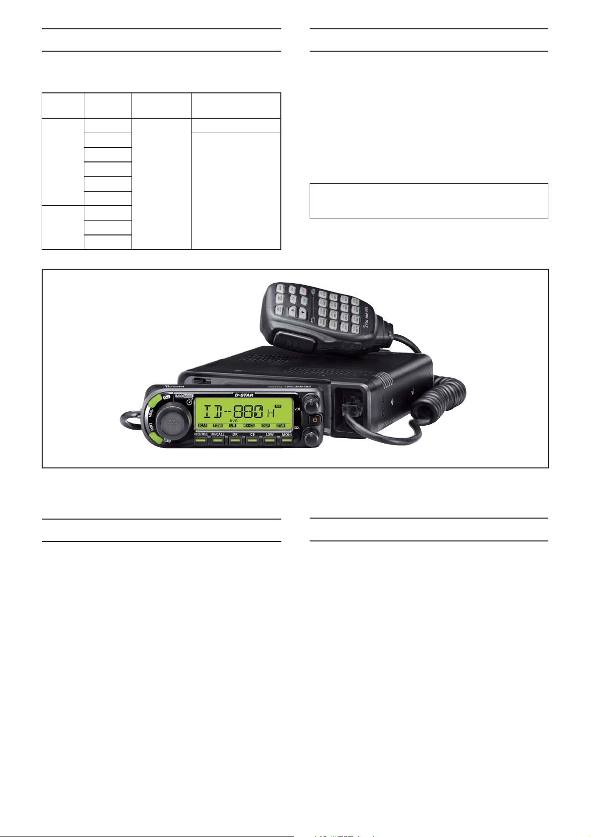
(ID-880H)
REPAIR NOTES
1. Make sure that the problem is internal before
disassembling the transceiver.
2. DO NOT open the transceiver until the transceiver is
disconnected from its power source.
3. DO NOT force any of the variable components. Turn
them slowly and smoothly.
4. DO NOT short any circuits or electronic parts. An
insulated tuning tool MUST be used for all adjustments.
5. DO NOT keep power ON for a long time when the
transceiver is defective.
6. DO NOT transmit power into a Standard Signal
Generator or a Sweep Generator.
7. ALWAYS connect a 50 dB to 60 dB attenuator between
the transceiver and a Deviation Meter or Spectrum
Analyzer when using such test equipment.
8. READ the instructions of test equipment throughly
before connecting a test equipment to the transceiver.
Icom, Icom Inc. and IDOM logo are registered trademarks of Icom Incorporated (Japan) in the United States, the United
Kingdom, Germany, France, Spain, Russia and/or other countries.
Page 3

TABLE OF CONTENTS
SECTION 1 SPECIFICATIONS
SECTION 2 INSIDE VIEWS
SECTION 3 DISASSEMBLY INSTRUCTION
SECTION 4 CIRCUIT DESCRIPITON
4-1 RECEIVER CIRCUITS. . . . . . . . . . . . . . . . . . . . . . . . . . . . . . . . . . . . . . . . . . . . . . . . . . . . . . . . 4-1
4-2 TRANSMITTER CIRCUITS . . . . . . . . . . . . . . . . . . . . . . . . . . . . . . . . . . . . . . . . . . . . . . . . . . . . 4-4
4-3 FREQUENCY SYNTHESIZER . . . . . . . . . . . . . . . . . . . . . . . . . . . . . . . . . . . . . . . . . . . . . . . . . 4-6
4-4 CPU (MAIN UNIT; IC25) PORT ALLOCATION . . . . . . . . . . . . . . . . . . . . . . . . . . . . . . . . . . . . . 4-7
4-5 VOLTAGE BLOCK DIAGRAM . . . . . . . . . . . . . . . . . . . . . . . . . . . . . . . . . . . . . . . . . . . . . . . . . . 4-8
SECTION 5 ADJUSTMENT PROCEDURE
5-1 PREPARATION . . . . . . . . . . . . . . . . . . . . . . . . . . . . . . . . . . . . . . . . . . . . . . . . . . . . . . . . . . . . . 5-1
5-2 FREQUENCY AND TRANSMIT AMPLIFIER ADJUSTMENTS. . . . . . . . . . . . . . . . . . . . . . . . . 5-3
5-3 ANALOG DEVIATION ADJUSTMENTS (VHF BAND). . . . . . . . . . . . . . . . . . . . . . . . . . . . . . . . 5-4
5-4 ANALOG DEVIATION ADJUSTMENTS (UHF BAND) . . . . . . . . . . . . . . . . . . . . . . . . . . . . . . . 5-5
5-5 DIGITAL DEVIATION ADJUSTMENT . . . . . . . . . . . . . . . . . . . . . . . . . . . . . . . . . . . . . . . . . . . . 5-6
5-6 RECEIVE SENSITIVITY ADJUSTMENT . . . . . . . . . . . . . . . . . . . . . . . . . . . . . . . . . . . . . . . . . . 5-7
5-7 S-METER ADJUSTMENT . . . . . . . . . . . . . . . . . . . . . . . . . . . . . . . . . . . . . . . . . . . . . . . . . . . . . 5-8
5-8 SQUELCH ADJUSTMENT . . . . . . . . . . . . . . . . . . . . . . . . . . . . . . . . . . . . . . . . . . . . . . . . . . . . 5-9
SECTION 6 PARTS LIST
SECTION 7 MECHANICAL PARTS
SECTION 8 BOARD LAYOUTS
SECTION 9 BLOCK DIAGRAM
SECTION 10 VOLTAGE DIAGRAM
CONTROL UNIT . . . . . . . . . . . . . . . . . . . . . . . . . . . . . . . . . . . . . . . . . . . . . . . . . . . . . . . . . . . . 10-1
MAIN UNIT. . . . . . . . . . . . . . . . . . . . . . . . . . . . . . . . . . . . . . . . . . . . . . . . . . . . . . . . . . . . . . . . . 10-2
Page 4
SECTION 1. SPECIFICATIONS
D GENERAL
• Frequency coverage :
<For ID-880H>
Version
U.S.A. 144–148, 430–450 118–173.995
CHN
136–173.995*1,
400–469.995*
EXP
KOR 144–146, 430–440 144–146, 430–440
AUS 144–148, 430–440 144–148, 430–440
TPE 144–146, 430–432 144–146, 430–432
*1Guaranteed 144–148 MHz only, *2Guaranteed 430–450 MHz only,
3
Guaranteed 430–440 MHz only, *4Not Guaranteed
*
<For ID-E880>
Version
EUR 144–146, 430–440 118–173.995
ITA
144–146, 430–434
EUR-1 144–146, 430–440 144–146, 430–440
*1Guaranteed 144–146 MHz only, *2Guaranteed 430–440 MHz only
3
Guaranteed 430–434 MHz only, *4Guaranteed 435–438 MHz only
*
5
Not guaranteed
*
• Type of emission : FM, AM (Receive only), DV
• Number of memory channels : 1052 (incl. 50 scan edges and 2 calls)
• Frequency resolution : 5
• Operating temperature range : –10°C to +60°C; +14˚F to +140˚F
• Frequency stability : ±2.5 ppm
• Power supply requirement : 13.8 V DC ±15%
• Current drain
Transmit at 50 W VHF: 11.5 A*
Receive standby 0.9 A
(simultaneous receive) max. audio 1.2 A
• Antenna connector : SO-239
• Dimensions (proj. not included) : 150(W) × 40(H) × 199.2(D) mm
• Weight
(at 13.8 V DC: approx.):
(approx.) : 1.3 kg; 2 lb 14 oz (not incl. cable)
:
TX RX
230–549.995
810–823.990
849–868.990
894–999.990
3
118–173.995
230–549.995
810–999.990
TX RX
230–549.995
810–999.990
435–438
118–173.995
230–549.995
810–999.990
‡
, 6.25‡, 8.33‡, 10, 12.5, 15‡, 20, 25,
30, 50, 100, 125, 200 kHz
‡
Selectable depending on the operating
frequency band.
(–10°C to +60°C)
UHF: 12.5 A*
* 8.0 A (at 25 W) only for the TPE version
(50 Ω)
29
⁄32(W)×19⁄16(H)×727⁄32(D) in
5
(unit: MHz)
*1,
*2,
*4,
*4,
4
*
*1,
*3,
4
*
(unit: MHz)
*1,
*2,
5
*
*1,
3, *4
*
,
5
*
D TRANSMITTER
• Modulation system :
FM
DV (DIgital) GMSK reactance frequency modulation
• Output power : 50/15/5 W*
• Max. frequency deviation : ±5.0 kHz (wide)
• Spurious emissions : Less than –60 dB
• Microphone connector : 8-pin modular
Variable reactance frequency modulation
(approx.)
*25/15/5 W only for the TPE version.
±2.5 kHz (narrow)
(600 Ω)
D RECEIVER
• Receive system : Double conversion superheterodyne
• Intermediate frequencies : 1st: 46.35 MHz, 2nd: 450 kHz
• Sensitivity
FM
DV
• Squelch sensitivity
• Selectivity
Wide More than 10 kHz/6 dB
Narrow More than 6 kHz/6 dB
Less than 20 kHz/60 dB
DV More than 50 dB
• Spurious and image rejection
AF output power† (at 13.8 V DC)
•
• Ext. speaker connectors : 3-conductor 3.5 (d) mm (1⁄8″)/8 Ω
(amateur bands only):
(12 dB SINAD) Less than 0.18 μV
(BER 1%) Less than 0.35 μV
†
(threshold) : Less than 0.13 μV
†
(typical) :
Less than 30 kHz/60 dB
†
: More than 60 dB
: More than 2.0 W at 10% distortion with an 8 Ω
load
†
Guaranteed 144–146 or 144–148 MHz and 430–440 or 440–450 MHz ranges only.
All stated specifications are subject to change without notice or obligation.
1 - 1
Page 5
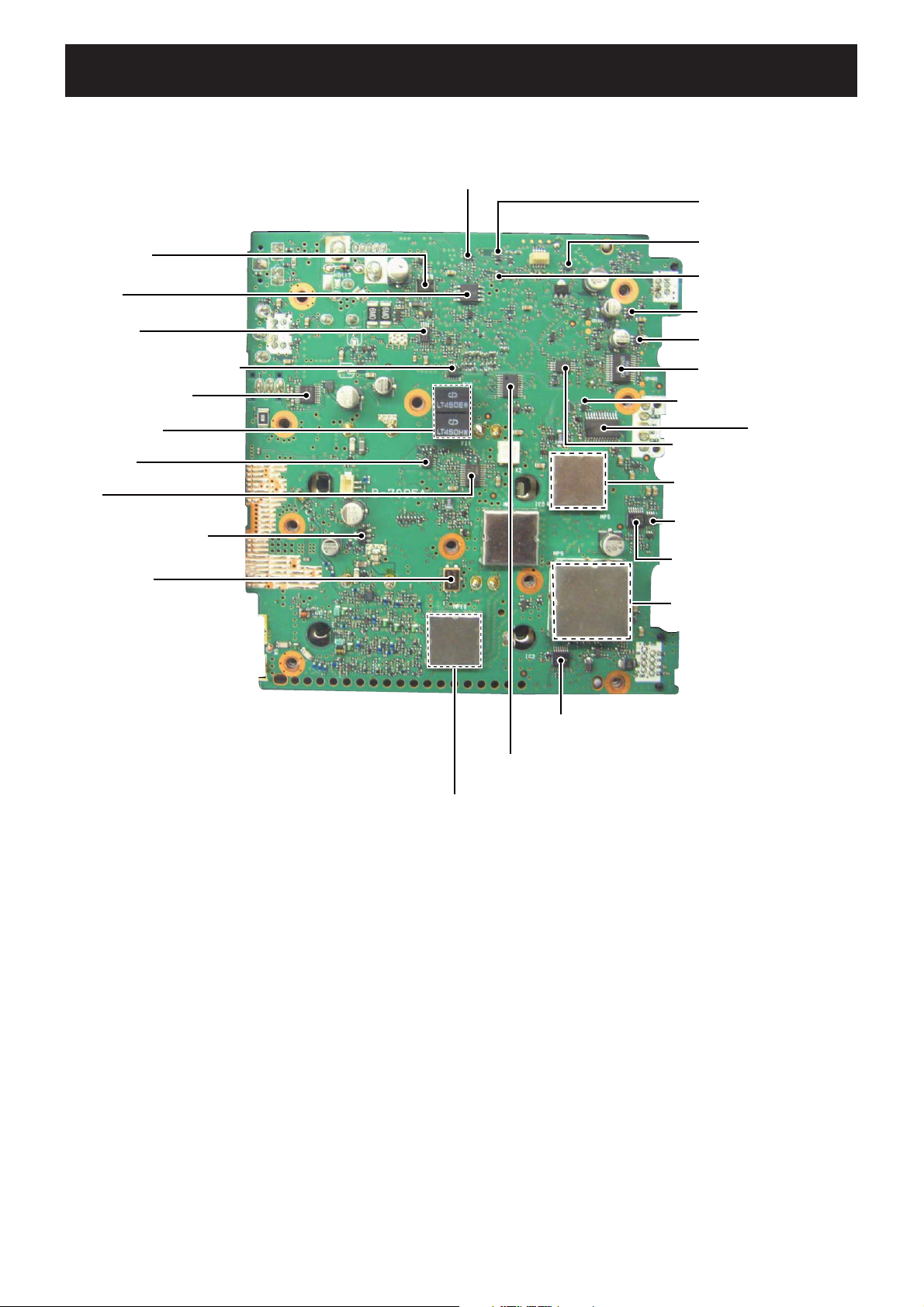
SECTION 2. INSIDE VIEWS
• MAIN UNIT
SQUELCH AMP
(IC65)
ELECTRIC VR
(IC66)
EEPROM
(IC22)
AF BUFFER
(IC49)
DIGITAL/ANALOG AF LINE SW
(IC11)
LEVEL CONVERTER
(IC46)
2ND IF FILTERS
(FI1; LT450HW, FI2; LT450EW)
AF SWITCH
(IC13)
IF IC
(IC15)
COOLING FAN DRIVER
(Q123)
1ST IF FILTER
(FI6)
LEVEL CONVERTER
(IC26)
LEVEL CONVERTER
(IC1001)
RESET IC
(IC23)
AMB_3.2V REGULATOR
(IC1004)
OP+5V REGULATOR
(IC1003)
MODEM
(IC1012)
MODULATION MUTE SWITCH
(IC9)
AF BUFFER
(IC1014)
UHF VCO
AF SW
(IC51)
AF LPF
(IC48)
VHF VCO
D/A CONVERTER
(IC8)
D/A CONVERTER
(IC1)
1ST IF MIXER CIRCUIT
MIC MUTE SWITCH
(IC30)
2 - 1
Page 6
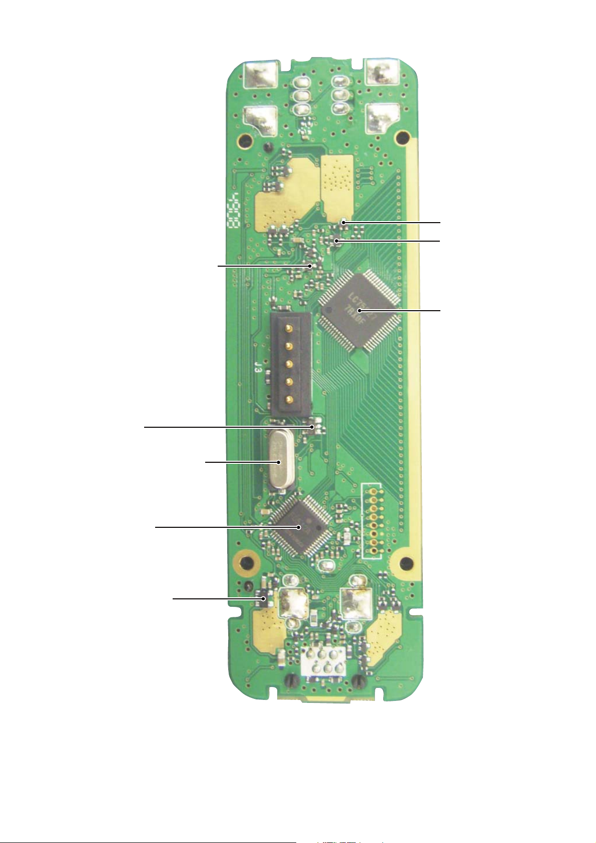
• CONTROL UNIT
LCD CONTRAST ADJUSTER
BACKLIGHT DRIVER
(Q1)
+5C REGULATOR
(Q16)
(Q15)
LCD DRIVER
(IC7)
RESET IC
(IC2)
CPU CLOCK (9.8304 MHz)
FRONT CPU
(IC4)
+5V REGULATOR
(IC8)
(X1)
2 - 2
Page 7
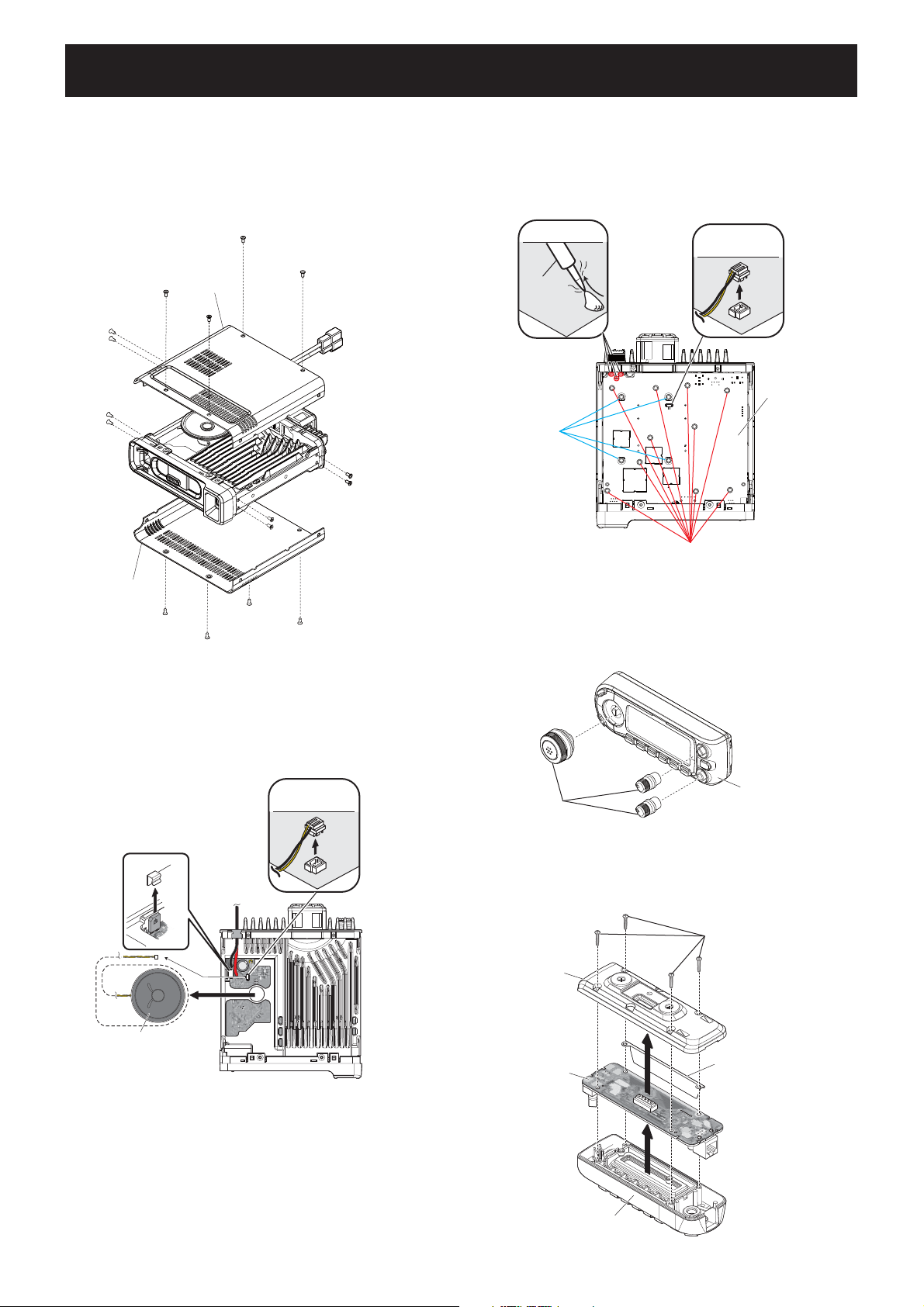
SECTION 3. DISASSEMBLY INSTRUCTION
1. REMOVING TOP AND BOTTOM COVERS
1) Unscrew total of 18 screws; 4 screws from the top cover,
8 screws from the both sides and 4 screws from the
bottom cover.
2) Remove the top cover and bottom cover as illustrated
below.
Top cover
Bottom cover
2. REMOVING THE MAIN UNIT (continued)
3) Unscrew 10 screws from the MAIN UNIT.
4) Unscrew 4 screws from the chassis.
5) Disconnect the cooling fan cable from the MAIN UNIT.
6) Unsolder total of 4 points, and take off the MAIN UNIT.
UNSOLDER
COOLING
FAN CABLE
Solder
remover
MAIN UNIT
Screw x4
Screw x10
<Bottom view>
2. REMOVING THE MAIN UNIT
1) Remove the IC clip from the chassis.
2) Disconnect the speaker cable from the MAIN UNIT, and
remove the speaker from the chassis.
SPEAKER
CABLE
IC clip
Speaker
3. DISASSEMBLE THE CONTROL UNIT
1) Remove 3 knobs from the front panel.
Knobs
2) Unscrew 4 screws from the rear panel.
3) Remove the LCD plate.
4) Take off the CONTROL UNIT from the front panel.
Rear panel
CONTROL UNIT
Front panel
Screw x4
LCD plate
<Top view>
(Continued to right above.)
Front panel
3 - 1
Page 8
SECTION 4. CIRCUIT DESCRIPTION
4-1 RECEIVE CIRCUITS
RF CIRCUITS
144 MHz BAND (118–174 MHz)
The RX signals (118–174 MHz) from the antenna are
passed through two LPFs and TX/RX SW for VHF band (D59,
68, 75, 77), and applied to the RF circuit.
The RX signals are passed through the limiter (D78, 79) and
BPF, and amplifi ed by the RF AMP (Q33). The amplifi ed RX
signals are filtered by tuned BPF (D41, 44, 60) to remove
unwanted signals, then applied to the 1st mixer (Q124).
The passband frequency of the tuned BPF (D41, 44, 60) is
tuned by the tuning voltage from the D/A converter controlled
by the CPU (IC25).
300 MHz BAND (230–420 MHz)
The RX signals (230–420 MHz) from the antenna are
passed through the LPF, HPF and TX/RX SW for UHF band
(D30, 53, 61, 62, 177), and applied to the RF circuit.
The RX signals are passed through the RX SW (D56) and
filtered by the tuned BPF (D57, 58) to remove unwanted
signals, then applied to the RF AMP (Q35).
The amplifi ed RX signals are fi ltered by another tuned BPF
(D45, 51) to remove unwanted signals, and amplified by
another RF AMP (Q34). The RF AMP (Q34) improves the
isolation between the 1st mixer (IC64) and the tuned BPF.
The amplifi ed RX signals are applied to the 1st mixer (IC64).
The pass-band frequencies of the tuned BPFs (D57, 58:
D45, 51) are tuned by the tuning voltage from the D/A
converter controlled by the CPU (IC25).
800 M Hz BAND (810–999 MHz)
The RX signals (810–999 MHz) from the antenna are
passed through the HPF, and applied to the RF AMP (Q28).
The amplifi ed RX signals are fi ltered by the tuned BPF (D18,
20) to remove unwanted signals, then applied to the 1st
mixer (IC64) via the RX SW (D9).
The pass-band frequency of tuned BPF (D18, 20) is tuned
by the tuning voltage from the D/A converter controlled by
the CPU (IC25).
• RF CIRCUITS
D59,68,75,77
RF
AMP
TX/RX
SW
D41,D44,D60
BPF
BPF1,2,3
D12,14,23
BPF
BPF1,2,3
D45,D51
BPF
BPF2,3
D30,53,61,62,177
TX/RX
SW
Q33
RF
AMP
Q19
RF
AMP
Q35
RF
AMP
BPF
D13
BPF
BPF1
D57,58
BPF
BPF1
LPF
HPF
UHFLPF
VHFLPF
D78,D79
LIMITER
<- 118-174 MHz
D16
RX
SW
<- 420-550 MHz
D56
RX
SW
<- 230-420 MHz
LPF
From VHF TX circuit
From UHF TX circuit
To the 1st IF mixer (Q124)
To the 1st IF mixer (Q125)
<- To the 1st IF mixer (IC64)
D36
Q34
RX
SW
440 MHz BAND (420–550 MHz)
The RX signals (420–550 MHz) from the antenna are
passed through the LPF, HPF and TX/RX SW for UHF band
(D30, 53, 61, 62, 177), and applied to the RF circuit.
The RX signals are passed through the RX SW (D16) and
tuned BPF (D13) to remove unwanted signals, and applied
to the RF AMP (Q19). The amplifi ed RX signals are fi ltered
by another tuned BPF (D12, 14, 23) to remove unwanted
signals, then applied to the 1st mixer (Q125).
The pass-band frequencies of tuned BPFs (D13: D12,
14, 23) are controlled by the tuning voltage from the D/A
converter controlled by the CPU (IC25).
<- To the 1st IF mixer (IC64)
D9
RX
SW
D18,D20
BPF
BPF2,3
Q28
RF
AMP
HPF
<- 810-999 MHz
4 - 1
Page 9
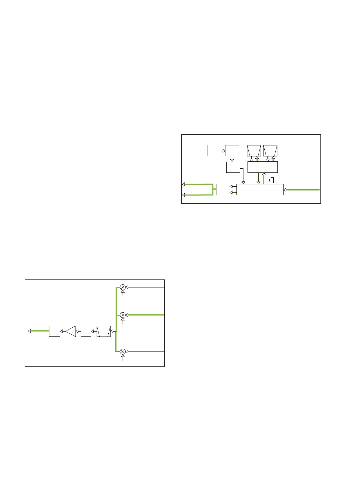
1st IF CIRCUITS
144 MHz BAND (118–174 MHz)
The RX signals (118–174 MHz) from the RF circuit are
applied to the G1 terminal of Q124 (1st IF mixer), and the
1st LO signals "140_LO" are applied to the G2 terminal of it.
2nd IF AND DEMODULATOR (for FM and AM) CIRCUITS
The 1st IF signal from the 1st IF circuits is applied to the
IF IC (IC15, pin 20). IC15 contains 2nd mixer, limiter AMP,
noise AMP, quadrature detector, RSSI circuit and AM
detector in its package.
These input signals are mixed to be converted into the
46.350 MHz 1st IF signal.
300 MHz (230–420 MHz) AND 800 MHz (810–999 MHz) BANDS
The RX signals (230–420 MHz and 810–999 MHz) from the
RF circuit are applied to the RX input terminal of IC64 (1st IF
mixer), and the 1st LO signals "UHF_LO" are applied to the
LO input terminal of it.
These input signals are mixed to be converted into the
46.350 MHz 1st IF signal.
440MHz BAND (420–550MHz)
The RX signals (420–550MHz) from the RF circuit are
applied to the G1 terminal of Q125 (1st IF mixer), and the
1st LO signals "440_LO" are applied to the G2 terminal of it.
These input signals are mixed to be converted into the
46.350 MHz 1st IF signal.
The 1st IF signal converted by the 1st mixer is passed
through the 1st IF fi lter (FI6) to remove unwanted signals.
FI6 is a 4-pole crystal filter contains two filters, and has
adequate selectivity to extract wanted signal.
The applied 1st IF signal is converted into the 450 kHz 2nd
IF signal by being mixed with tripled reference frequency
signal (45.9 MHz) from the PLL IC (IC14) via the tripler (Q52).
The converted 2nd IF signal is output from pin 3, and passed
through the ceramic fi lter (FI1 for FM narrow and AM modes,
FI2 for FM and DV modes) to remove sideband noise, then
applied to the IF IC (from pin 7; FM/DV mode/ from pin 5; AM
mode) again.
• 2ND IF CIRCUITS
450 kHz 2nd IF filter
FI1
PLL
IC
Q52
X3
45.9 MHz
2nd LO
Pin 11(FM/DV mode)
Pin 14(AM mode)
FI2
(For wide)
CERAMIC
BPF
WIDE/NARROW
(For narrow)
SELECTOR
IF IC
CERAMIC
BPF
X2
IC15
From the 1st IF circuits
X5
To the AF filter circuits
(FM/AM mode)
To the digital demodulator circuits
(DV mode)
TCXO
15.3 MHz
IC13
DETECT
SIGNAL
SELECTOR
IC14
The fi ltered 1st IF signal is applied to the 1st IF AMP (Q66)
via the limiter (D1009), and the amplified 1st IF signal is
applied to the IF IC (IC15) via another limiter (D88).
• 1ST IF CIRCUITS
From the 140 MHz band
Q124
RF circuit
140_LO
From the 440 MHz band
Q125
RF circuit
To the 2nd IF
circuits
D88
LIMIT
Q66
IF
AMP BPF
D1009
LIMIT
FI6
XTAL
46.35MHz
440_LO
From the 300 MHz and
IC64
800 MHz bands RF circuit
UHF_LO
4 - 2
Page 10
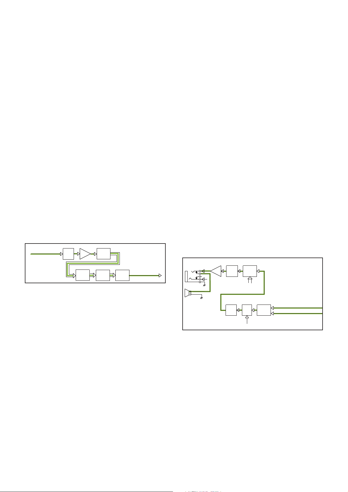
FM DEMODULATOR CIRCUITS
In the FM mode, the filtered 2nd IF signal input from
pin 7 is amplified by the internal limiter amplifier, and FMdemodulated at the internal quadrature detector. The
demodulated AF signals are then output from pin 11 and
applied to the AF circuits via the AF switch (IC13).
AM DEMODULATOR CIRCUITS
In the AM mode, the filtered 2nd IF signal input from
pin 5 is amplified by the internal limiter amplifier, and AMdemodulated at the internal AM detector. The demodulated
AF signals are output from pin 14 and applied to the AF fi lter
circuits via the AF switch (IC13).
DIGITAL (DV) DEMODULATOR CIRCUITS
In the DV mode, the filtered 2nd IF signal input from
pin 7 is amplified by the internal limiter amplifier, and
FM-demodulated at the internal quadrature detector.
The demodulated AF signals are applied to the digital
demodulator circuits via the AF switch (IC13).
AF FILTER CIRCUITS
The demodulated AF signals are applied to the AF filter
(Q47) via the digital/analog signal selector (IC11), to obtain
suitable audio response the for receive mode (FM, AM or
DV).
The frequency response of the fi lter is controlled by “AFFIL_
SEL” signal from the CPU (IC25).
The fi ltered AF signals are applied to the variable pass-band
frequency audio filter circuit (IC49a; pins 3, 1). The circuit
reduces audible noises included in the demodulated AF
signals.
The fi ltered AF signals are applied to the electric volume IC
(IC66) which adjusts the loudness by “AF_VOL_DATA” and
“AF_VOL_CK” signals from the CPU (IC25).
The level-adjusted AF signals are applied to the AF power
AMP (IC38) via the AF mute SW (Q102).
The FM-demodulated AF signals from the AF switch (IC13)
are applied to the modem (IC1012) via the two buffers (IC49b;
pins 6, 7 and IC1014), and converted into the digital signal.
The converted digital signal is applied to the DSP CODEC
(IC1) via the level converter (IC1000, 1001, 1002), to be
decoded into the AMBE signal. The decoded AMBE signal is
then applied to the liner CODEC IC (IC1006) to be converted
into the analog audio signal. The converted AF signals are
applied to the RX AF circuits.
• DIGITAL (DV) DEMODULATOR CIRCUITS
From the FM demodulator
circuits (DV mode)
IC49b
BUFF
IC1000,1001,1002
LEVEL
BUFF
CNV.
IC1014
IC1012
MODEM
IC1006
CODEC
IC1013
To the AF filter circuits
(DV mode)
DSP
LINEAR
CODEC
AF POWER AMPLIFIER
The AF signals from the AF mute SW (Q102) are applied to
the AF power AMP (IC38), and amplifi ed to obtain AF output
power. The power-amplified AF signals are applied to the
internal speaker (CHASSIS; SP1) via J8.
If an external speaker is connected to the external speaker
jack (J8), the power-amplifi ed AF signals from the AF power
AMP (IC38) are applied to the connected speaker via J8.
• AF FILTER CIRCUITS AND AF POWER AMPLIFIER
[EXTERNAL SPEAKER JACK]
J8
SP1
Internal speaker
IC38
AF
AMP
Q102
MUTE
FILTER
IC66
SP
Volume
control
AF_VOL_DATA
AF_VOL_CK
IC11Q47IC49a
From the FM/AM demodulator circuits
AF
AF
FILTER
AFFIL_SEL
(FM/AM mode)
DIGI/AN
SELECT
From the digital demodulator circuits
(DV mode)
4 - 3
Page 11
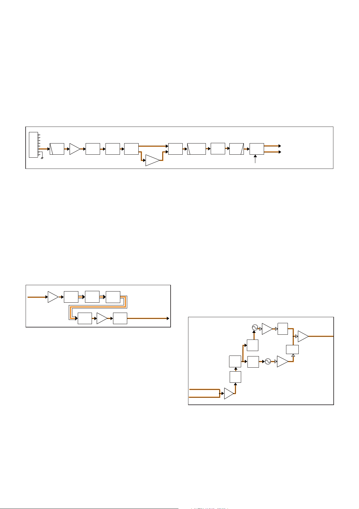
4-2 TRANSMITTER CIRCUITS
TX AF CIRCUITS
MIC signals from the connected microphone are passed
through the HPF (Q87), and amplified by the MIC AMP
(IC28). The amplified MIC signals are passed through the
MIC gain SW (Q88) which selects the MIC sensitivity from
“High” or “Low,” and the MIC mute SW (IC30), then passed
through or bypassed the ALC AMP (IC32) via the AF SWs
(IC29 and IC52).
In the DV mode, the MIC signals are applied to the ALC
AMP (IC32) which automatically adjusts the level of MIC
signals for digital processing,
• TX AF CIRCUITS
J2
1
2
3
Q87
4
5
MIC
6
7
8
From the microphone
Q88
IC28
MIC
HPF
AMP
MIC GAIN
SWITCH
IC30
IC29 IC52
MIC
MUTE
AF
SW
ALC
AMP
IC32
The MIC signals from the AF SW (IC52) are passed through
the pre-emphasis and IDC (for amplitude-limitting) circuits
(IC48b), MIC level adjustment circuit (IC48a) and the
splatter circuit (IC48d) which cuts off the 3 kHz and higher
audio signals. The filtered MIC signals are applied to the
modulation circuits via the AF SW (IC51; pins 1, 7).
In the DV mode, the filtered MIC signals are applied to
the digital converter circuits before being applied to the
modulation circuits via the AF SW (IC51; pins 1, 6).
To the modulation circuits
IC48b
Pre-emphasis
AF
SW
IC48a
and IDC
Level
ADJ.
IC48d
SPLATTER
IC51
(FM mode)
AF
SW
To the digital converter circuits
(DV mode)
DA_SEL
DIGITAL CONVERTER CIRCUITS
The MIC signals from the TX AF circuits are applied to
the liner CODEC IC (IC1013) via the buffer (IC1014), and
encoded into the digital audio signal. The encoded digital
audio signal is then applied to the DSP CODEC IC (IC1006)
and converted into the AMBE signal. The AMBE signal
is applied to the modem (IC1012) via the level converter
(IC1000, 1001,1002). The modem IC converts the AMBE
signal into the analog signal, and output to the modulation
circuits via the buffer (IC1015) and the digital/analog line SW
(IC34).
• DIGITAL CONVERTER CIRCUITS
From the TX AF
circuits
IC1014
BUFF
IC1013
LINEAR
CODEC
IC1006
IC1012
MODEM
DSP
CODEC
IC1000,1001,1002
IC1015
BUFF
LEVEL
CNV.
IC34
To the modulation circuits
Digi/Ana
line SW
MODULATION CIRCUITS
The AF signals from the TX AF circuits (in FM mode) or
digital converter circuits (in DV mode) are applied to the AF
AMP (IC48c). The amplifi ed modulation signals are passed
through the D/A converter (IC8) to be adjusted its level
(=deviation), then applied to the VCO (VHF VCO: Q111,
D145–148/UHF VCO: Q73, D87, 91, 92) via the modulation
mute SWs (IC9, VHF; Q109/UHF; Q64) as the modulation
signals.
The modulated VCO oscillating signal is passed through the
buffer (VHF; Q113/UHF; Q76) and applied to the LO AMP
(IC45) via the VCO SW (VHF; D160, 175/UHF; D102).
The amplified VCO output signals are applied to the TX
amplifi er circuits.
• MODULATION CIRCUITS
Q113
BUFF
UHF VCO
Q73
D87,91,92
D160,D175
VCO
SW
D102
Q76
BUFF
IC45
To the TX amplifer
circuits
LO
AMP
VCO
SW
From the TX AF
circuits (FM mode)
From the digital converter
circuits (DV mode)
IC48c
AMP
IC9
IC8
MOD
MUTE
D/A
Q111
D145-148
Q109
VHF VCO
MOD
MUTE
Q64
MOD
MUTE
4 - 4
Page 12
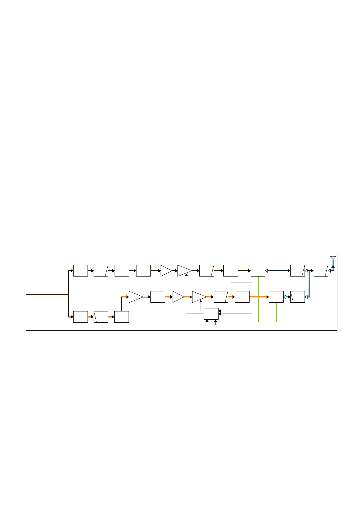
TX AMPLIFIER CIRCUITS (VHF BAND)
The output signal of VHF VCO (Q111, D145–148) is passed
through the LO SW (D155), LPF and ATT, then applied to
the drive AMP (Q25) via the limiter (D29), to obtain adequate
input level for the power AMP (power MOS-FET module;
IC3).
The amplifi ed TX signal is power-amplifi ed to 50 W (approx.;
25 W for [TPE] ver.) of output power (max.) by the power
AMP (IC3).
TX AMPLIFIERS (UHF BAND)
The output signal of UHF VCO (Q73, D87, 91, 92) is passed
through the LO SW (D103), HPF and ATT, then applied to
the pre-drive AMP (Q22). The amplifi ed TX signal is applied
to the drive AMP (Q26) via the limiter (D25) and amplifi ed to
obtain adequate input level for the power AMP (power MOSFET module; IC2).
The amplifi ed TX signal is power-amplifi ed to 50 W (approx.;
25 W for [TPE] ver.) of output power by the power AMP (IC2).
The power-amplified TX signal is passed through the LPF
which attenuates harmonic components to prescribed level,
then applied to the antenna connector via the power detector
(D39, 47, 1005), TX/RX SW (D59, 68, 75, 77) and two LPFs.
APC CIRCUITS (VHF BAND)
A portion of the TX signal from IC3 is rectifi ed at the power
detector (D39, 47, 1005), and converted into the DC voltage
which is in proportion to the RF power, and applied to the
operational amplifi er (IC4, pin 6). IC4 is an APC amplifi er for
both of V/UHF bands. The TX power setting voltage “PCON_
V” from the D/A converter (IC1) is applied to the pin 5 as
a reference. IC4 is rolled as a differential amplifier which
outputs voltage in inverse proportion to rectifi ed one.
When the TX power increased, the rectified voltage also
increased, that causes the decrease of output voltage of
differential amplifier. The decrease of output voltage of
differential amplifi er causes the drop of the gate voltage of
IC3, Thus the TX power maintained to keep stable level.
• TX AMPLIFIER AND APC CIRCUITS
VHF band TX signal ->
D155
LO SW
D29
ATTLPF LPF
LIMITER
DRIVE
AMP
Q25
The power-amplified TX signal is passed through the LPF
which attenuates harmonic components to prescribed level,
then applied to the antenna connector via the power detector
(D42, 52, 1006), TX/RX SW (D30, 53, 61, 62, 177), HPF and
LPF.
APC CIRCUITS (UHF BAND)
A portion of the TX signal from IC2 is rectifi ed at the power
detector (D42, 52, 1006), and converted into the DC voltage
which is in proportion to the RF power, and applied to the
operational amplifi er (IC4, pin 2). IC4 is an APC amplifi er for
both of V/UHF bands. The TX power setting voltage “PCON_
U” from the D/A converter (IC1) is applied to the pin 3 as
a reference. IC4 is rolled as a differential amplifier which
outputs voltage in inverse proportion to rectifi ed one.
When the TX power increased, the rectified voltage also
increased, that causes the decrease of output voltage of
differential amplifier. The decrease of output voltage of
differential amplifi er causes the drop of the gate voltage of
IC2, Thus the TX power maintained to keep stable level.
PWR
AMP
IC3
D39,D47,D1005
LPF
PWR
DET
D59,68,75,77
TX/RX
SW
LPF
From the frequency synthesizer
circuits
UHF TX signal ->
D103
LO SW
HPF
D25
Q22
PRE
DRIVE
ATT
LIMITER
DRIVE
AMP
Q26
T
IC2
PWR
AMP
PCON_U PCON_V
IC4
APC
CTRL
D42,52,1006
PWR
DET
D30,53,61,62,177
TX/RX
SW
To UHF RX circuitsTo VHF RX circuits
HPFLPF
4 - 5
Page 13
4-3 FREQUENCY SYNTHESIZER
VCOs
VHF VCO
The VHF VCO is composed by the oscillator circuit (Q111,
D145, 146, 147) and buffer AMP (Q113), and generates
both of 1st LO signals and TX signal for VHF band.
The VCO oscillating signals are buffer-amplified by Q113,
amplifi ed by the LO AMP (IC45) to obtain adequate LO level,
then applied to the TX amplifi ers or 1st IF mixer via the LO
SW, ATT and fi lter.
While transmitting;
The VCO output signals from the LO AMP (IC45) are applied
to the TX amplifi ers via the LO SW (D155) as the TX signal.
While receiving;
The VCO output signals from the LO AMP (IC45) are passed
through the LO SW (D170), ATT and the LPF, then applied to
the 1st IF mixer (Q124), as the 1st LO signals for 140 MHz
band.
PLL
The PLL circuit provides stable oscillation of the transmit
frequency and receive 1st LO frequency. The PLL output
frequency is controlled by control signals including divide
ratio (“PLLCK,”"PLLDATA”and "PLLSTB") from the CPU
(IC25).
PLL (VHF VCO)
A portion of VHF VCO output signals from the buffer
(Q113) are applied to the PLL IC (IC14) via the VCO switch
(D175). The applied signals are divided at the prescaler and
programmable counter.
The divided signal is phase-compared with the 15.3 MHz
reference frequency signal from the reference frequency
oscillator (X5), at the phase detector.
The phase difference is output from pin 5 as a pulse type
signal after being passed through the internal charge pump.
The VCO output signals from the LO AMP (IC45) are passed
through the LO SW (D104), ATT, RF SW and LPF, then
applied to the 1st IF mixer (Q125), as the 1st LO signals for
300 MHz band.
UHF VCO
The UHF VCO is composed by the oscillator circuit (Q73,
D87, 91, 92) and buffer AMP (Q76), and generates both of
1st LO signals and TX signal for UHF band.
The VCO oscillating signals are buffer-amplified by Q76,
amplifi ed by the LO AMP (IC45) to obtain adequate LO level,
then applied to the TX amplifi ers or 1st IF mixer via the LO
SW, ATT and fi lter.
While transmitting;
The VCO output signals from the LO AMP (IC45) are applied
to the TX amplifi ers via the LO SW (D103) as the TX signal.
While receiving;
The VCO output signals from the LO AMP (IC45) are passed
through the LO SW (D101), ATT, doubler (HPF) and LPF,
then applied to the 1st IF mixer (IC64), as the 1st LO signals
for 800 MHz band.
The VCO output signals from the LO AMP (IC45) are passed
through the LO SW (D179), ATT and the LPF, then applied to
the 1st IF mixer (IC64), as the 1st LO signals for 440 MHz band.
The output signal is converted into the DC voltage (lock
voltage) by passing through the loop fi lter (R694-698, C759-
763). The lock voltage is applied to the variable capacitors
(D145, 146), and locked to keep the VCO frequency
constant.
PLL (UHF VCO)
A portion of VHF VCO output signals from the buffer (Q76)
are applied to the PLL IC (IC14) via the VCO switch (Q1015).
The applied signals are divided at the prescaler and
programmable counter.
The divided signal is phase-compared with the 15.3 MHz
reference frequency signal from the reference frequency
oscillator (X5), at the phase detector.
The phase difference is output from pins 15 and 16, and
passed through the external charge pump (Q61, 62) to be
converted into the pulse type signal.
The output signal is converted into the DC voltage (lock
voltage) by passing through the loop fi lter (R355, 362, 365,
369, 378, C451, 456, 473). The lock voltage is applied to the
variable capacitors (D91, 92), and locked to keep the VCO
frequency constant.
• FREQUENCY SYNTHESIZER CIRCUITS
PLLCK
PLLDATA
PLLSTB
X5
15.3MHz
TCXO
IC14
LOOP
FIL
PLL
IC
45.9 MHz
IF IC
IC15
IC1018
VCO
SELECT
Q52
X3
Q61,62
LOOP
FIL
VHF VCO
Q110,111
D145-148
UHF VCO
Q73
D87,91,92
Q113
BUFF
Q76
BUFF
D160,D175
VCO
SW
Q 1015
BUFF
D155
LO SW
D103
LO SW
D170
IC45
LO
AMP
D102
VCO
SW
LO SW
-> RX LO signals for 140 MHz band (118-174 MHz) ->
D179
LO SW
-> RX LO signals for 440 MHz band (420-550 MHz) ->
D101
LO SW
-> RX LO signals for 800MHz band (810-999 MHz) ->
D104
LO SW
-> RX LO signals for 300 MHz band (230-420 MHz) ->
To VHF TX Aamplifier
To UHF TX Aamplifier
ATT
X2
ATT
(HPF)
Q79
RF
ATT
SW
LPF
LPFATT
D181
LPF
LO SW
D180
LPF
LO SW
Q124
140 MHz band
1st IF MIXER
Q125
440 MHz band
1st IF MIXER
IC64
800 MHz and
300 MHz bands
1st IF MIXER
4 - 6
Page 14

4-4 CPU (MAIN UNIT; IC25) PORT ALLOCATION
PIN
No.
3
4
5
6
8
9
10
11
16
17
22
23
24
25
26
28
29
32
33
34
35
36
37
38
39
48
52
55
LINE NAME
AN
DA_SEL
MM_MUTE
DCONT
1200_
9600SEL
P_PTT
P_SQL
MIC_SENC
DADJSEL
MOD_DA
PLLSTB
AMC
DTCS_SEL
R5C
WN_SEL
UTX_C
VCO_SHIFT
PLLCK
PLLDATA
UNLOCK
MMUTE
VTX_C
PLLSW
UVCO_SEL
VVCO_SEL
D5VC
AFFIL_SEL
DTCS
Audio response select signal.
"H"=FM mode.
"L"=DV mode.
Cut-off frequency shifting signal to the
HPF (IC48).
MIC mute signal to the MIC mute switch
(IC30).
"H"=MIC mute.
ALC amplifier control signal to the AF
switches (IC29 and IC52).
"H"=ALC amplifi er ON.
Baud rate select signal to the packet
modulation select switch (IC30).
Packet PTT detect signal. I
Packet squelch control signal. O
Microphone sensitivity select signal.
"H"=High sensitivity.
Modulation mute signal to the digital
modulation switch (IC34).
Modulation line switching signal to the
MOD mute switches (IC9 and IC67).
"H"=Modulation enable.
Strobe signal to the PLL IC ( IC14). O
AM-demodulator circuit control signal.
"L"= While receiving in AM mode (AM-
modulator and AGC circuits are
activated).
Tone filter switching signal to the
LPF (Q100).
"H"=DTCS mode.
"L"=CTCSS mode.
RX circuits control signal.
"H"=RX circuits is activated.
2nd IF filter (Wide/Narrow) toggling
signal.
"H"=Narrow.
"L"=Wide.
Transmitting control signal to the UT8 line
regulator (Q13, 17).
"H"=While transmitting in UHF band.
VCO oscillating frequency shift signal to
the VHF VCO switch (Q110).
Clock signal to the PLL IC (IC14). O
Data to the PLL IC (IC14). O
PLL unlock signal from the PLL IC ( IC41). I
Modulation mute signal to the MOD mute
switch (Q64).
"H"=Modulation muted.
Transmitting control signal to the VT8 line
regulator (Q12, 15).
"H"=While transmitting in VHF band.
Lock-up time control signal to the loop
fi lter.
"H"=Fast lock-up time.
VCO power control signal to the VCO
select switch (Q65, 68).
"L"=UHF VCO is activated.
VCO power control signal to the VCO
select switch (Right band VHF; Q65, 68).
"H"=VHF VCO is activated.
Power control signal for the digital
converter circuits.
Switching signal to the AF fi lter (Q47).
"H"=FM
"L"=AM/DV
DTCS and CTCS signals. O
DESCRIPTION I/O
O
O
O
O
O
O
O
O
O
O
O
O
O
O
O
O
O
O
O
O
PIN
No.
56
57
62
63
64
65
66
69
70
71
76
77
78
80
82
85
101
103
107
108
109
110
111
112
113
114
115
116
122
123
127
128
129
130
131
132
134
142
143
144
LINE NAME
DTMF
MIC_SEL
MICUD
AMRSSI
RSSI
IDET
HVin
WXALT
DTCS_IN
TEMP
SCL
AF_VOL_CK
AF_VOL_
DATA
PWR
SDA
MIC_PTT
SQL
CL_SFT1
ACQ
98_DATA
TXDT
TXCK
RXDT
RXCK
AMBERES
AMBECLK
AMBEEPR
AMBESTB
RX_DATA
TX_DATA
TX232
RX232
DA_CK
DA_DATA
AMBETXD
AMBETRD
DA_STB
MOD_MUTE
FIL1(143pin)
FIL2(144Pin)
DESCRIPTION I/O
Beep, DTMF and european tone (E880
only) signals.
Connected microphone detect signal. I
[UP]/[DWN] key input from connected
microphone (HM-154).
Inputs RSSI signal (for AM mode) from
the AGC line controller (Q44).
While receiving; inputs RSSI signal from
the IF IC (IC15).
Current level from the current detector
(IC55, D163).
Divided voltage of the HV line. I
Demodulated Weather alert signal from
the AF fi lter. ([USA] only)
Demodulated CTCSS and DTCS signals
from the CTCSS fi lter (Q41).
Transceiver's internal temparature from
the thermal detector circuit (R509).
I/O port for clock signal to the EEPROM
(IC22).
Serial clock signal to the electric volume
IC (IC66).
Data signal to the electric volume IC
(IC66).
Power control signal to the PWR controller
(Q82).
"H"=While the transceiver power is ON.
Data signal to the EEPROM (IC22). I/O
Input port for [PTT] key on the connected
microphone.
Noise signal from the IF IC (IC15). I
Clock frequency shift signal. O
ACQ signal to the modem IC (IC1012). O
Communication signal to the connected
microphone (HM-133).
TX data (DV) to the modem IC (IC1012). O
TX clock signal (DV) to the modem IC
(IC1012).
RX data (DV) to the modem IC (IC1012). I
RX clock signal (DV) to the modem IC
(IC1012).
Reset signal to the DSP CODEC (IC1006). O
Clock signal to the DSP CODEC (IC1006). O
EPR (Encode Packet Ready) signal to the
DSP CODEC (IC1006).
Strobe signal to the DSP CODEC (IC1006).
Data lines for the control unit. I
Data lines for the control unit. O
Data bus for RS-232C communication. O
Data bus for RS-232C communication. I
Serial clock signal to the D/A converter. O
Serial data to the D/A converter. O
AMBE RX signal. I
AMBE TX signal. O
Strobe signal to the D/A converter. O
Packet modulation mute signal. O
AF fi lter circuits control signals. O
O
I/O
O
O
O
I/O
O
O
O
I
I
I
I
I
I
I
I
I
4 - 7
Page 15
4-5 VOLTAGE BLOCK DIAGRAM
Voltage from the power supply is routed to the whole of the transceiver via regulators and switches.
MAIN UNIT
IC3
CONTROL UNIT
NOISE
FILTER
IC21
5V
REG
IC55,
D164
CURRENT
DETECT
NOISE
FIL
Q83,
D119
5VS
REG
D120
Q84,
5VS
REG
HV
TX power
amplifiers (IC2, IC3)
IDET
CPU5V
5V
CPU (IC25)
(for current monitoring)
CPU (IC25),
EEPROM (IC22),
Reset IC (IC23), etc.
PLL IC (IC14),
5VS
D/A converter (IC8),
ALC IC (IC32), etc.
DTMF decoder (IC56),
L5V
Electric volume (IC33),
AF mixer (IC59), etc.
Limitter (D165−D168), etc.
HV
+5
REG
+3
REG
+3.2V
5V
CPU (IC13),
Regulator (Q14, Q15),
Protector/Buffer (IC12), etc.
Reset IC (IC9),
LCD module, etc.
PWR
Q82
PWR
CTRL
Q81
VCC
REG
IC24
+8
REG
AF filter (Q47, Q50),
8V
MIC amplifier (IC28),
APC controller (IC4), etc.
VCC
AF power amplifier (IC38)
4 - 8
Page 16
SECTION 5. ADJUSTMENT PROCEDURE
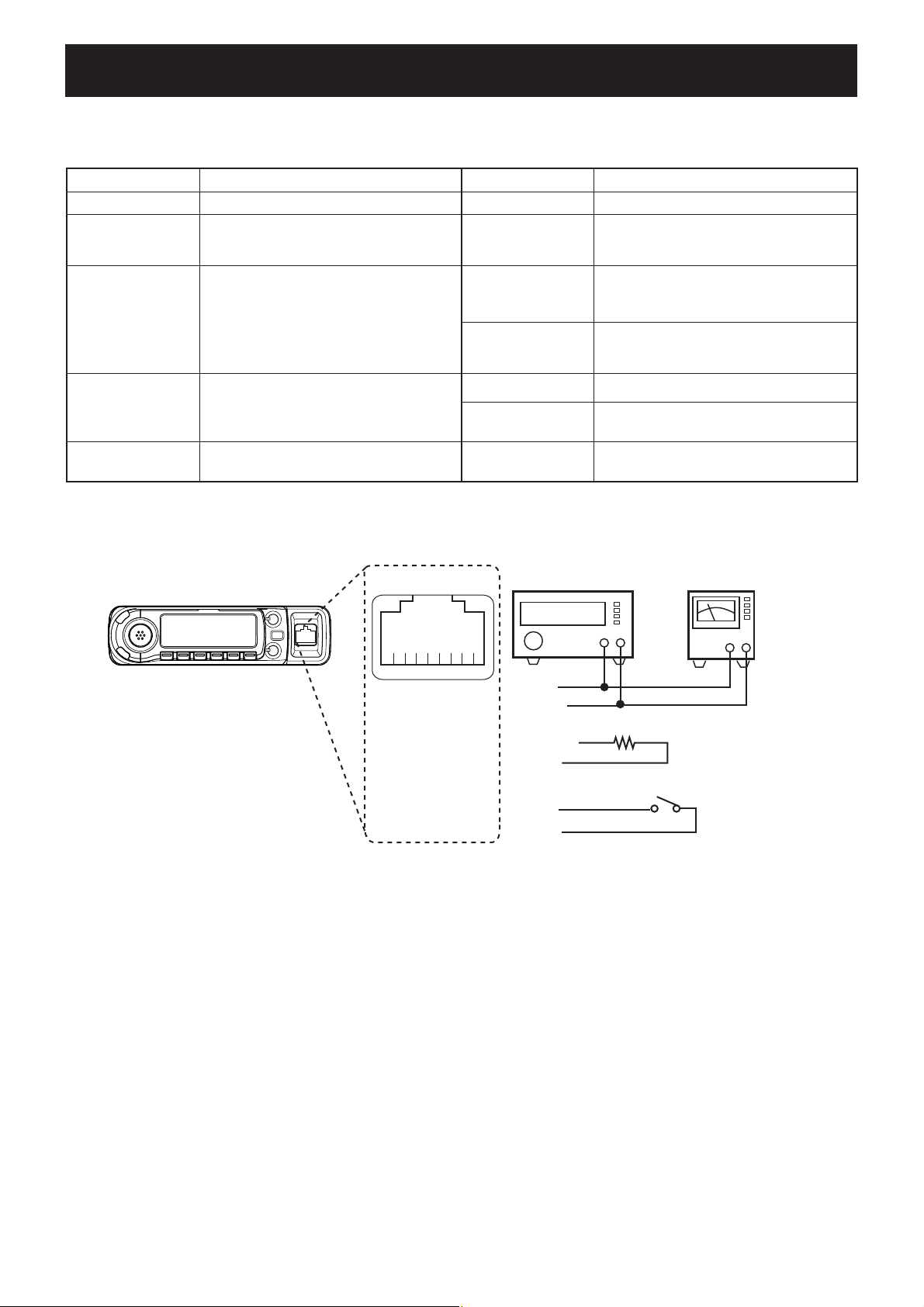
5-1 PREPARATION
¤ REQUIRED INSTRUMENTS
INSTRUMENTS SPECIFIDATION INSTRUMENTS SPECIFIDATION
DC Cable (Supplied with transceiver) JIG cable
Output voltages : 13.8 V DC
Power Supply
and 12.0 V DC
Multimeter
Current capacity : More than 15 A
RF Power Meter
(terminated type)
Measuring range : 0.1–60 W
Except [TPE]
0.1–30 W [TPE]
Frequency range : 100–600 MHz
Impedance : 50
Ω
Standard Signal
Generator (SSG)
Terminator Impedance : 50
SWR : Less than 1.2 : 1
AC Millivoltmeter Measuring range : 10 mV to 10 V
Attenuator
Audio generator
Frequency counter
Modulation
Analyzer
Frequency range : 0.1–600 MHz
Frequency accuracy :
±0.1 ppm or better
Input level : Less than 1 mW
Frequency range : 30–600 MHz
Measuring range : 0 to ±10 kHz
(See the illust below)
Input impedance : 50 kΩ
Measuring range : 0.1–20V/0.01–5 A
Frequency range : 0.1–1200 MHz
Output level : 0.04 µV to 32 mV
(–28 dBu to 90 dBu)
Power attenuation : 40 dB
Capacity : More than 100 W
Frequency range : 300–3000 Hz
Output level : 1–500 mV
Ω
M JIG CABLE
To [MICROPHONE CONNECTOR]
8-pin modular jack
ytre
i
u
q
w
e
r
t
y
u
i
8V
MICU/D
EXTMIC
PTT
MICE
MIC
GND
MICIN
q
w
AUDIO GENERATOR
(300–3000 Hz/1–500 mV)
+−
y (MIC)
t (MICE)
22 kΩ
w (MICU/D)
u (GND)
r (PTT)
u (GND)
AC MILLIVOLTMETER
(10 mV to 10 V)
+−
PTT
5 - 1
Page 17

CONNECTION
M
Oscilloscope
Standard signal generator
–127 to –17 dBm
(0.1 V to 32 mV)
CAUTION:
DO NOT transmit while
SSG is connected to
the antenna connector.
Modulation analyzer
(DC measurable)
40 dB or 50 dB
Terminator
(50 Ω)
Attenuator
JIG CABLE
(See the page 5-1)
RF power meter
60 W Except [TPE]
30 W [TPE]
DC power supply
13.8 V / 15 A
DC power supply
12.0 V / 15 A
(For “CURRENT PROTECT
REFERENCE”)
To [MICROPHONE CONNECTOR]
Frequency
counter
to the antenna connector
to DC cable
to DC cable
[DC13.8V]
[ANT]
M ENTERING ADJUSTMENT MODE
q Turn the transceiver power OFF.
w Connect
e Push and hold [MONI] and [BAND], turn the transceiver power ON.
Entering adjustment mode, the function display shows the adjustment item and conditions as below.
<Rotating>
Adjusts the value for the item manually.
JIG cable
(See the page 5-1)
to the [MICROPHONE CONNECTOR].
Adjustment frequency, mode and TX power
BAND
U
N
E
M
S
.
M
W
M
W
<Pushing>
• Store the set value.
• Adjusts the value for
the item automatically.
Selects next adjustment item.
MODE
VFO/MHz
M/CALL CSDR LOW
VOL
SQL
MONI
Adjustment item
ATTENTION: NEVER change the value of the
adjustment items that are not described in this
ADJUSTMENT PROCEDURES. Otherwise, the
transceiver may not work properly.
Connects the JIG cable
(See the page 5-1)
Selects previous adjustment item.
QUITTING ADJUSTMENT MODE
M
• Disconnect the JIG cable, then turn the transceiver power OFF.
5 - 2
Page 18

5-2 FREQUENCY AND TRANSMIT AMPLIFIER ADJUSTMENT
Select an adjustment item using [VFO/MHz] / [M/CALL], then set the adjustment value as specifi ed using [DIAL].
ADJUSTMENT
REFERENCE
FREQUENCY
VHF BAND
TRANSMIT POWER
[Hi power]
(BAND LOW)
(BAND HIGH)
[Mid power]
(BAND LOW)
(BAND HIGH)
[Low power]
(BAND LOW)
(BAND HIGH)
VHF BAND
CURRENT PROTECT
REFERENCE
[BAND LOW]
[BAND HIGH]
UHF BAND
TRANSMIT POWER
[Hi power]
(BAND LOW)
(BAND HIGH)
[Mid power]
(BAND LOW)
(BAND HIGH])
[Low power]
(BAND LOW)
(BAND HIGH)
UHF BAND
CURRENT PROTECT
REFERENCE
(BAND LOW)
(BAND HIGH)
1)
Except [USA], [AUS], [CHN], [EXP]
2)
[USA], [AUS], [CHN], [EXP]
ADJUSTMENT
ITEM
[REF]
[PHL]
[PHH]
[PML]
[PMH]
[PLL]
[PLH]
[PHL]
[PHH] 3
[PHL]
[PHH]
[PML]
[PMH]
[PLL]
[PLH]
[PHL]
[PHH] 3
OPERATION VALUE
1 1) Connect an RF power meter to the antenna connector.
2) Loose couple a frequency counter to the antenna
connector.
3) While transmitting, adjust the TX frequency using [DIAL],
then push [BAND] to store the adjustment value.
1• Connect an RF power meter to the antenna connector.
2• While transmitting, adjust the TX power using [DIAL], then
push [BAND] to store the adjustment value.
3
4
1 1) Set the power supply voltage to 12.0 V.
2) Connect an RF power meter to the antenna connector.
2• While transmitting, push [BAND] to store the adjustment
value.
435.0000 MHz
440.0000 MHz
(Except [TPE])
(Except [TPE])
1)
2)
–
50 W
25 W ([TPE])
15 W
5 W
–
(Automatic
adjustment)
–
50 W
25 W ([TPE])
15 W
5 W
–
(Automatic
adjustment)
5 - 3
Page 19

5-3 ANALOG DEVIATION ADJUSTMENTS (VHF BAND)
Select an adjustment item using [VFO/MHz] / [M/CALL], then set the adjustment value as specifi ed using [DIAL].
ADJUSTMENT
VHF BAND
FM DEVIATION
[BAND LOW] (FM)
[BAND LOW] (FMN)
[BAND HIGH] (FM)
[BAND HIGH] (FMN)
VHF BAND
MODULATION
BALANCE
[BAND LOW] (FM)
[BAND LOW] (FMN)
[BAND HIGH] (FM)
[BAND HIGH] (FMN)
ADJUSTMENT
ITEM
[FMS]
[FMB]
OPERATION VALUE
1 1) Connect a modulation analyzer to the antenna connector
through an attenuator, and set is as;
HPF : OFF
LPF : 20 kHz
De-emphasis : OFF
Detector : (P-P)/2
2) Connect an audio generator and an AC millivoltmeter to
the JIG cable
2 1) Set the audio generator as;
Frequency : 1 kHz
3 ±2.1 kHz
Level : 80 mVrms [USA]
4 ±4.2 kHz
: 20 mVrms Except [USA]
2) While transmitting, adjust the deviation using [DIAL], then
5
push [BAND] to store the adjustment value.
1 1) No audio signals are applied.
2) Connect an oscilloscope to the modulation analyzer.
2• While transmitting, adjust the waveform using [DIAL], then
push [BAND] to store the adjustment value.
3
4
5
(See the page 5-1)
.
–
±4.2 kHz
±2.1 kHz
–
Set to square
waves
DTCS DEVIATION
[VHF BAND] (FM)
[VHF BAND] (FMN)
CTCSS DEVIATION
[VHF BAND] (FM)
[VHF BAND] (FMN)
[MDT]
[MCT]
1 1) Connect a modulation analyzer to the antenna connector
through an attenuator, and set is as;
HPF : OFF
LPF : 20 kHz
De-emphasis : OFF
Detector : (P-P)/2
2) No audio signals are applied.
2• While transmitting, adjust the deviation using [DIAL], then
push [BAND] to store the adjustment value.
3• Push [VFO/MHz] to skip this item. –
±0.80 kHz
±0.75 kHz
–
–
5 - 4
Page 20

5-4 ANALOG DEVIATION ADJUSTMENTS (UHF BAND)
Select an adjustment item using [VFO/MHz] / [M/CALL], then set the adjustment value as specifi ed using [DIAL].
ADJUSTMENT
UHF BAND
FM DEVIATION
[BAND LOW] (FM)
[BAND LOW] (FMN)
[BAND HIGH] (FM)
[BAND HIGH] (FMN)
VHF BAND
MODULATION
BALANCE
[BAND LOW] (FM)
[BAND LOW] (FMN)
[BAND HIGH] (FM)
[BAND HIGH] (FMN)
ADJUSTMENT
ITEM
[FMS]
[FMB]
OPERATION VALUE
1 1) Connect a modulation analyzer to the antenna connector
through an attenuator, and set is as;
HPF : OFF
LPF : 20 kHz
De-emphasis : OFF
Detector : (P-P)/2
2) Connect an audio generator and an AC millivoltmeter to
the JIG cable
2 1) Set the audio generator as;
Frequency : 1 kHz
3 ±2.1 kHz
Level : 80 mVrms [USA]
: 20 mVrms Except [USA]
4 ±4.2 kHz
2) While transmitting, adjust the deviation using [DIAL], then
5
push [BAND] to store the adjustment value.
1 1) No audio signals are applied.
2) Connect an oscilloscope to the modulation analyzer.
2• While transmitting, adjust the waveform using [DIAL], then
push [BAND] to store the adjustment value.
3
4
5
(See the page 5-1)
.
Set to square wave
–
±4.2 kHz
±2.1 kHz
–
DTCS DEVIATION
[UHF BAND] (FM)
[UHF BAND] (FMN)
CTCSS DEVIATION
[UHF BAND] (FM)
[UHF BAND] (FMN)
[MDT]
[MCT]
1 1) Connect a modulation analyzer to the antenna connector
through an attenuator, and set is as;
HPF : OFF
LPF : 20 kHz
De-emphasis : OFF
Detector : (P-P)/2
2) No audio signals are applied.
4• While transmitting, adjust the deviation using [DIAL], then
push [BAND] to store the adjustment value.
5• Push [VFO/MHz] to skip this item. –
±0.80 kHz
±0.75 kHz
–
–
5 - 5
Page 21

5-5 DIGITAL DEVIATION ADJUSTMENT
Select an adjustment item using [VFO/MHz] / [M/CALL], then set the adjustment value as specifi ed using [DIAL].
ADJUSTMENT
VHF BAND
DV DEVIATION
(BAND LOW)
(BAND HIGH)
VHF BAND
DV MODULATION
BALANCE
(BAND LOW)
(BAND HIGH)
UHF BAND
DV DEVIATION
(BAND LOW)
(BAND HIGH)
UHF BAND
DV MODULATION
BALANCE
(BAND LOW)
(BAND HIGH)
ADJUSTMENT
ITEM
[MDS]
[MDB]
[MDS]
[MDB]
OPERATION VALUE
1• Connect a modulation analyzer to the antenna connector
through an attenuator, and set is as;
HPF : OFF
LPF : 20 kHz
De-emphasis : OFF
Detector : (P-P)/2
2• While transmitting, adjust the deviation using [DIAL], then
push [BAND] to store the adjustment value.
3
1 1) Connect a modulation analyzer to the antenna connector
through an attenuator, and set is as;
HPF : OFF
LPF : 20 kHz
De-emphasis : OFF
Detector : (P-P)/2
2) Connect an oscilloscope to the modulation analyzer.
2• While transmitting, adjust the deviation using [DIAL], then
push [BAND] to store the adjustment value.
3
–
±1.2 kHz
–
Minimum deviation
–
±1.2 kHz
–
Minimum deviation
5 - 6
Page 22

5-6 RECEIVE SENSITIVITY ADJUSTMENT
1) Select an adjustment item using [VFO/MHz] / [M/CALL].
2) Set the SSG as specifi ed (frequency, deviation and output level).
3) Push [BAND] to adjust (automatic) and store the adjustment value.
ADJUSTMENT
RECEIVE
SENSITIVITY
†
; This output level of a standard signal generator (SSG) is indicated as SSG’s open circuit.
ADJUSTMENT
ITEM
[LT1]
[MT1]
[HT1]
[LT2]
[MT2]
[HT2]
[LT3]
[MT3]
[HT3]
[UT3]
[LT4]
[MT4]
[HT4]
[UT4]
[LT5]
[MT5]
[HT5]
OPERATION VALUE
1• Connect an SSG to the antenna connector and set as;
Modulation : 1 kHz
Deviation : 3.5 kHz
Level : 0 dBµ (–107 dBm)
2 • Set the SSG as;
Frequency : (Displayed on the function display)
3 • Set the SSG as;
Frequency : (Displayed on the function display)
4 • Set the SSG as;
Frequency : (Displayed on the function display)
5 • Set the SSG as;
Frequency : (Displayed on the function display)
6 • Set the SSG as;
Frequency : (Displayed on the function display)
7 • Set the SSG as;
Frequency : (Displayed on the function display)
8 • Set the SSG as;
Frequency : (Displayed on the function display)
9 • Set the SSG as;
Frequency : (Displayed on the function display)
10 • Set the SSG as;
Frequency : (Displayed on the function display)
11 • Set the SSG as;
Frequency : (Displayed on the function display)
12 • Set the SSG as;
Frequency : (Displayed on the function display)
13 • Set the SSG as;
Frequency : (Displayed on the function display)
14 • Set the SSG as;
Frequency : (Displayed on the function display)
15 • Set the SSG as;
Frequency : (Displayed on the function display)
16 • Set the SSG as;
Frequency : (Displayed on the function display)
17 • Set the SSG as;
Frequency : (Displayed on the function display)
18 • Set the SSG as;
Frequency : (Displayed on the function display)
†
Push [BAND]
(Automatic
adjustment)
5 - 7
Page 23

5-7 S-METER ADJUSTMENT
1) Select an adjustment item using [VFO/MHz] / [M/CALL].
2) Set the SSG as specifi ed (frequency and output level).
3) Push [BAND] to adjust (automatic) and store the adjustment value.
ADJUSTMENT
S-METER
(S3 level)
[VHF band 1]
(S3 level)
[VHF band 1] (FMN)
(Full scale)
[VHF band 1]
(Full scale)
[VHF band 1] (FMN)
(S3 level)
[VHF band 2]
(S3 level)
[VHF band 2] (FMN)
(Full scale)
[VHF band 2]
(Full scale)
[VHF band 2] (FMN)
(S3 level)
[UHF band 1]
(S3 level)
[UHF band 1] (FMN)
(Full scale)
[UHF band 1]
(Full scale)
[UHF band 1] (FMN)
(S3 level)
[UHF band 2]
(S3 level)
[UHF band 2] (FMN)
(Full scale)
[UHF band 2]
(Full scale)
[UHF band 2] (FMN)
(S3 level)
[UHF band 3]
(S3 level)
[UHF band 3] (FMN)
†
; This output level of a standard signal generator (SSG) is indicated as SSG’s open circuit.
(FM)
(FM)
(FM)
(FM)
(FM)
(FM)
(FM)
(FM)
(FM)
ADJUSTMENT
ITEM
[S31]
[S31]
[SF1]
[SF1]
[S32]
[S32]
[SF2]
[SF2]
[S33]
[S33]
[SF3]
[SF3]
[S34]
[S34]
[SF4]
[SF4]
[S35]
[S35]
OPERATION VALUE
1• Connect an SSG to the antenna connector and set as;
Modulation : None
2 • Set the SSG as;
Frequency : (Displayed on the function display)
Level : –2 dBµ (–109 dBm)
3 • Set the SSG as;
Frequency : (Displayed on the function display)
Level : –2 dBµ (–109 dBm)
4 • Set the SSG as;
Frequency : (Displayed on the function display)
Level : +12 dBµ (–95 dBm)
5 • Set the SSG as;
Frequency : (Displayed on the function display)
Level : +12 dBµ (–95 dBm)
6 • Set the SSG as;
Frequency : (Displayed on the function display)
Level : –2 dBµ (–109 dBm)
7 • Set the SSG as;
Frequency : (Displayed on the function display)
Level : –2 dBµ (–109 dBm)
8 • Set the SSG as;
Frequency : (Displayed on the function display)
Level : +12 dBµ (–95 dBm)
9 • Set the SSG as;
Frequency : (Displayed on the function display)
Level : +12 dBµ (–95 dBm)
10 • Set the SSG as;
Frequency : 300.020 MHz
Level : –2 dBµ (–109 dBm)
11 • Set the SSG as;
Frequency : (Displayed on the function display)
Level : –2 dBµ (–109 dBm)
12 • Set the SSG as;
Frequency : (Displayed on the function display)
Level : +12 dBµ (–95 dBm)
13 • Set the SSG as;
Frequency : 300.020 MHz
Level : +12 dBµ (–95 dBm)
14 • Set the SSG as;
Frequency : (Displayed on the function display)
Level : –2 dBµ (–109 dBm)
15 • Set the SSG as;
Frequency : (Displayed on the function display)
Level : –2 dBµ (–109 dBm)
16 • Set the SSG as;
Frequency : (Displayed on the function display)
Level : +12 dBµ (–95 dBm)
17 • Set the SSG as;
Frequency : (Displayed on the function display)
Level : +12 dBµ (–95 dBm)
18 • Set the SSG as;
Frequency : (Displayed on the function display)
Level : –2 dBµ (–109 dBm)
19 • Set the SSG as;
Frequency : (Displayed on the function display)
Level : –2 dBµ (–109 dBm)
†
†
†
†
†
†
†
†
†
†
†
†
†
†
†
†
†
†
Push [BAND].
(Automatic
adjustment)
5 - 8
Page 24

5-7 S-METER ADJUSTMENT (continued)
1) Select an adjustment item using [VFO/MHz] / [M/CALL].
2) Set the SSG as specifi ed (frequency and output level).
3) Push [BAND] to adjust (automatic) and store the adjustment value.
ADJUSTMENT
(Full scale)
[UHF band 3]
(Full scale)
[UHF band 3] (FMN)
†
; This output level of a standard signal generator (SSG) is indicated as SSG’s open circuit.
(FM)
ADJUSTMENT
ITEM
[SF5]
[SF5]
OPERATION VALUE
20 • Set the SSG as;
Frequency : (Displayed on the function display)
Level : +12 dBµ (–95 dBm)
21 • Set the SSG as;
Frequency : (Displayed on the function display)
Level : +12 dBµ (–95 dBm)
†
†
5-8 SQUELCH ADJUSTMENT
1) Select an adjustment item using [VFO/MHz] / [M/CALL].
2) Push [BAND] to adjust (automatic) and store the adjustment value.
ADJUSTMENT
SQUELCH
[VHF band 1] (FM)
[VHF band 1] (FMN)
[VHF band 2] (FM)
[VHF band 2] (FMN)
[UHF band 1] (FM)
[UHF band 1] (FMN)
[UHF band 2] (FM)
[UHF band 2] (FMN)
[UHF band 3] (FM)
[UHF band 3] (FMN)
ADJUSTMENT
ITEM
[SQ1]
[SQ1] 2
[SQ2] 3
[SQ2] 4
[SQ3] 5
[SQ3] 6
[SQ4] 7
[SQ4] 8
[SQ5] 9
[SQ5] 10
OPERATION VALUE
1• Connect a terminator to the antenna connector.
Push [BAND].
(Automatic
adjustment)
Push [BAND].
(Automatic
adjustment)
5 - 9
Page 25

SECTION 6. PARTS LIST
[CONTROL UNIT]
REF PARTS
NO. NO.
IC2 1110005991 S.IC S-80945CNMC-G9F-T2G B 49.5/15.5
IC4 1140014930 S.IC UPD78F0512AGA(R)-GAM-AX B 31.9/13.4
IC7 1130014930 S.IC LC75827W-E B 69.8/24
IC8 1180003460 S.REG NJM2831F05-TE1-#ZZZB B 18.9/6.7
Q1 1530003990 S.TRA 2SC4738-BL(TE85L,F) B 85.2/21.4
Q6 1530003990 S.TRA 2SC4738-BL(TE85L,F) B 92.3/9.6
Q7 1530003990 S.TRA 2SC4738-BL(TE85L,F) B 8/24.4
Q8 1530003990 S.TRA 2SC4738-BL(TE85L,F) B 95/11.1
Q9 1530003990 S.TRA 2SC4738-BL(TE85L,F) B 10.5/24.4
Q10 1530003990 S.TRA 2SC4738-BL(TE85L,F) B 84.1/8.7
Q11 1530003990 S.TRA 2SC4738-BL(TE85L,F) B 17.4/27.7
Q12 1530003990 S.TRA 2SC4738-BL(TE85L,F) B 84.1/10.7
Q13 1530003990 S.TRA 2SC4738-BL(TE85L,F) B 17.4/30.1
Q14 1530003990 S.TRA 2SC4738-BL(TE85L,F) B 80.2/15.5
Q15 1510000771 S.TRA 2SA1586-GR(TE85L,F) B 77.8/15.2
Q16 1510000771 S.TRA 2SA1586-GR(TE85L,F) B 82.3/20.2
D4 1790001001 S.ZEN MAZ8062GLL B 30/21.5
D5 1790001251 S.DIO MA2S1110GL B 78.3/17.2
D8 1790001251 S.DIO MA2S1110GL B 14.2/17.6
D9 1790001251 S.DIO MA2S1110GL B 11.8/12.3
D10 1790001251 S.DIO MA2S1110GL B 15.8/19.1
D11 1790001251 S.DIO MA2S1110GL B 13.2/19.3
D12 1790001251 S.DIO MA2S1110GL B 71.3/8.9
D13 1790001251 S.DIO MA2S1110GL B 4.4/15.1
D14 1790001251 S.DIO MA2S1110GL B 21.5/8.8
D15 1790001830 S.VAR AVR-M1005C270MTAAB B 75.6/12.2
D16 1790001830 S.VAR AVR-M1005C270MTAAB T 58.6/8.4
D17 1790001830 S.VAR AVR-M1005C270MTAAB T 64.4/9.2
D18 1790001830 S.VAR AVR-M1005C270MTAAB T 51.1/12
X1 6050012471 S.XTA CR-836A(SMD-49/9.8304 MHz)
<JJE> B 44.1/10.2
R3 7210003340 VAR R0903N-B50K L-20F 50K
R4 7030005120 S.RES ERJ2GEJ 102 X (1K) B 35.5/20.2
R7 7210003340 VAR R0903N-B50K L-20F 50K
R8 7030005120 S.RES ERJ2GEJ 102 X (1K) B 33.7/20.2
R13 7030005050 S.RES ERJ2GEJ 103 X (10K) B 84.1/17.3
R20 7030005530 S.RES ERJ2GEJ 100 X (10) B 8.3/11.4
R21 7030009280 S.RES ERJ2GEJ 391 X B 84.7/19.3
R22 7030005170 S.RES ERJ2GEJ 474 X (470K) B 76.1/19
R24 7030005050 S.RES ERJ2GEJ 103 X (10K) B 12.1/13.4
R25 7030005050 S.RES ERJ2GEJ 103 X (10K) B 13.4/20.5
R41 7030005160 S.RES ERJ2GEJ 105 X (1M) B 36/8.2
R42 7030005120 S.RES ERJ2GEJ 102 X (1K) B 92.6/7.7
R43 7030005120 S.RES ERJ2GEJ 102 X (1K) B 11.5/22.7
R44 7030005570 S.RES ERJ2GEJ 820 X (82) B 91.7/7.7
R45 7030005570 S.RES ERJ2GEJ 820 X (82) B 6.5/24.4
R46 7030005120 S.RES ERJ2GEJ 102 X (1K) B 95.5/9.1
R47 7030005120 S.RES ERJ2GEJ 102 X (1K) B 12/24.1
R48 7030005570 S.RES ERJ2GEJ 820 X (82) B 94.5/9.1
R49 7030005570 S.RES ERJ2GEJ 820 X (82) B 5.6/25.2
R50 7030005120 S.RES ERJ2GEJ 102 X (1K) B 82.2/8.2
R51 7030005120 S.RES ERJ2GEJ 102 X (1K) B 19.1/27.6
R52 7030005570 S.RES ERJ2GEJ 820 X (82) B 85.5/13.1
R53 7030005570 S.RES ERJ2GEJ 820 X (82) B 20.1/28.4
R54 7030005120 S.RES ERJ2GEJ 102 X (1K) B 82.2/10.2
R55 7030005120 S.RES ERJ2GEJ 102 X (1K) B 19/29.6
R56 7030005570 S.RES ERJ2GEJ 820 X (82) B 84.4/12.2
R57 7030005570 S.RES ERJ2GEJ 820 X (82) B 20.2/29.6
R58 7030005220 S.RES ERJ2GEJ 223 X (22K) B 74.9/18.6
R59 7030005220 S.RES ERJ2GEJ 223 X (22K) B 74.7/15.7
R60 7030005220 S.RES ERJ2GEJ 223 X (22K) B 73.9/14.8
R65 7030007290 S.RES ERJ2GEJ 222 X (2.2K) T 49.3/2.7
R66 7030007290 S.RES ERJ2GEJ 222 X (2.2K) T 73.6/3
R67 7030007570 S.RES ERJ2GEJ 122 X (1.2K) T 7.2/2.3
R72 7030005120 S.RES ERJ2GEJ 102 X (1K) T 33.2/12
R73 7030005120 S.RES ERJ2GEJ 102 X (1K) T 36.1/11.3
R76 7030005050 S.RES ERJ2GEJ 103 X (10K) B 82/16.1
R77 7030005170 S.RES ERJ2GEJ 474 X (470K) B 77.2/13.4
R78 7030005120 S.RES ERJ2GEJ 102 X (1K) B 28/20.2
R79 7030007350 S.RES ERJ2GEJ 393 X (39K) B 72.7/13.7
R83 7030005050 S.RES ERJ2GEJ 103 X (10K) B 48.7/17.7
R100 7030005220 S.RES ERJ2GEJ 223 X (22K) B 81.3/14.1
R101 7030005240 S.RES ERJ2GEJ 473 X (47K) B 71.2/14.2
R102 7030005050 S.RES ERJ2GEJ 103 X (10K) B 35.1/21.4
R110 7030007270 S.RES ERJ2GEJ 151 X (150) T 38.8/20.5
R111 7030007270 S.RES ERJ2GEJ 151 X (150) T 38.5/19.6
R112 7030007270 S.RES ERJ2GEJ 151 X (150) T 43.2/21.7
R113 7030007270 S.RES ERJ2GEJ 151 X (150) T 45.5/21.7
R114 7030007270 S.RES ERJ2GEJ 151 X (150) T 52.8/19.6
R115 7030007270 S.RES ERJ2GEJ 151 X (150) T 50.2/20
R116 7030007270 S.RES ERJ2GEJ 151 X (150) T 67.7/19.5
R117 7030007270 S.RES ERJ2GEJ 151 X (150) T 65.5/19.5
R120 7030005120 S.RES ERJ2GEJ 102 X (1K) B 82.6/24.1
R121 7030005120 S.RES ERJ2GEJ 102 X (1K) B 82.6/23
R122 7030005120 S.RES ERJ2GEJ 102 X (1K) B 84.2/24.7
R123 7030005120 S.RES ERJ2GEJ 102 X (1K) B 84.2/23.6
R124 7030007290 S.RES ERJ2GEJ 222 X (2.2K) T 94.8/2.7
R125 7030000010 S.RES MCR10EZHJ JPW (000) B 15.5/15.5
R126 7030005090 S.RES ERJ2GEJ 104 X (100K) B 82.4/18.4
R127 7030005050 S.RES ERJ2GEJ 103 X (10K) T 61.9/9.1
DESCRIPTION
M.
H/V
LOCATION
[CONTROL UNIT]
REF PARTS
NO. NO.
R128 7030005050 S.RES ERJ2GEJ 103 X (10K) T 59.8/9.1
R129 7030005090 S.RES ERJ2GEJ 104 X (100K) B 32/8
R130 7030005090 S.RES ERJ2GEJ 104 X (100K) B 31.8/5.1
R131 7030005090 S.RES ERJ2GEJ 104 X (100K) B 30.9/4.2
R132 7030005090 S.RES ERJ2GEJ 104 X (100K) B 28.4/6.8
R133 7030005120 S.RES ERJ2GEJ 102 X (1K) T 51.8/11.1
R134 7030005120 S.RES ERJ2GEJ 102 X (1K) B 9.4/12.4
R135 7030005050 S.RES ERJ2GEJ 103 X (10K) B 29.8/23.2
R136 7030005050 S.RES ERJ2GEJ 103 X (10K) B 31.9/23.3
R137 7030005050 S.RES ERJ2GEJ 103 X (10K) B 27.1/23.5
R138 7030005050 S.RES ERJ2GEJ 103 X (10K) B 32.2/22.4
R139 7030005090 S.RES ERJ2GEJ 104 X (100K) B 15.3/20.1
R140 7030005090 S.RES ERJ2GEJ 104 X (100K) B 13.3/14.2
R141 7030010040 S.RES ERJ2GEJ-JPW T 38/11.6
R142 7030010040 S.RES ERJ2GEJ-JPW B 37.7/13
R146 7030010040 S.RES ERJ2GEJ-JPW B 27.9/18
R147 7030009280 S.RES ERJ2GEJ 391 X B 98/11.8
R148 7030009280 S.RES ERJ2GEJ 391 X B 98.5/10.7
R149 7030009280 S.RES ERJ2GEJ 391 X B 23.3/27.4
R150 7030009280 S.RES ERJ2GEJ 391 X B 23.3/28.3
R151 7030005120 S.RES ERJ2GEJ 102 X (1K) B 76.8/11.9
R152 7030005120 S.RES ERJ2GEJ 102 X (1K) T 60.7/9.1
R153 7030005120 S.RES ERJ2GEJ 102 X (1K) T 63.2/9.4
R154 7030007570 S.RES ERJ2GEJ 122 X (1.2K) T 9.4/8.9
C2 4030016790 S.CER ECJ0EB1C103K B 34.6/20.2
C4 4030016790 S.CER ECJ0EB1C103K B 32.8/20.2
C5 4030017430 S.CER ECJ0EC1H101J B 83.7/16.1
C7 4030017430 S.CER ECJ0EC1H101J B 12.2/15.1
C8 4030017430 S.CER ECJ0EC1H101J B 82.4/17.4
C10 4030017430 S.CER ECJ0EC1H101J B 12.2/20.6
C16 4030016790 S.CER ECJ0EB1C103K B 31.7/6.3
C24 4030019500 S.CER GRM21BB31A106KE18
(GRM40 B) B 8.2/9.7
C25 4030016790 S.CER ECJ0EB1C103K B 23.2/7.9
C26 4030017040 S.CER ECJ0EB1A333K B 47.1/14.3
C27 4030017460 S.CER ECJ0EB1E102K B 21.4/7.8
C28 4030019120 S.CER GRM188B31E105KA75D B 21.7/6.7
C29 4030017460 S.CER ECJ0EB1E102K B 3.8/17
C30 4030017420 S.CER ECJ0EC1H470J B 12.2/16
C31 4030017420 S.CER ECJ0EC1H470J B 11.3/20.5
C34 4030016790 S.CER ECJ0EB1C103K B 80.4/18.7
C35 4030016930 S.CER ECJ0EB1A104K B 75.8/16.9
C36 4030016930 S.CER ECJ0EB1A104K B 74.3/16.6
C37 4030016930 S.CER ECJ0EB1A104K B 74.1/17.5
C42 4030017460 S.CER ECJ0EB1E102K B 53.1/8
C43 4030017460 S.CER ECJ0EB1E102K B 75.9/13.4
C44 4030017460 S.CER ECJ0EB1E102K T 35.2/11.1
C45 4030017460 S.CER ECJ0EB1E102K T 37/11.6
C46 4030017460 S.CER ECJ0EB1E102K B 19.2/15.8
C48 4030016930 S.CER ECJ0EB1A104K B 76.7/17.2
C49 4030017460 S.CER ECJ0EB1E102K B 72.7/12.8
C50 4030016790 S.CER ECJ0EB1C103K B 30/20.1
C51 4030016790 S.CER ECJ0EB1C103K B 80.3/9.9
C52 4030019120 S.CER GRM188B31E105KA75D B 82.4/13.2
C53 4030016790 S.CER ECJ0EB1C103K B 101/14.6
C54 4030017490 S.CER C1608 JB 1A 105K-T B 34.5/7.2
C55 4030017400 S.CER ECJ0EC1H220J B 50.6/8.6
C56 4030017400 S.CER ECJ0EC1H220J B 37.7/8.4
C57 4030017420 S.CER ECJ0EC1H470J B 26.9/18.9
C58 4030017420 S.CER ECJ0EC1H470J B 26.8/17.1
C59 4030017420 S.CER ECJ0EC1H470J B 26.3/16.2
C60 4030017420 S.CER ECJ0EC1H470J B 30.6/7.2
C61 4030017420 S.CER ECJ0EC1H470J B 30.1/6.3
C62 4030017420 S.CER ECJ0EC1H470J B 28.7/7.7
C63 4030017420 S.CER ECJ0EC1H470J B 27.3/8.5
C64 4030017420 S.CER ECJ0EC1H470J B 26.1/9.3
C65 4030017420 S.CER ECJ0EC1H470J B 27.3/9.4
C66 4030017420 S.CER ECJ0EC1H470J B 26.8/19.9
J2 6510023170 CON 3008L-6P6C <KIN>
J3 6510027270 CON 3167 FRONT CONNECTOR
<CCP>
DS1 5040003470 S.LED HT-297UY/UYG <SHO> T 37/20.6
DS2 5040003470 S.LED HT-297UY/UYG <SHO> T 59.2/20.6
DS4 5040003470 S.LED HT-297UY/UYG <SHO> T 44.4/20.6
DS5 5040003470 S.LED HT-297UY/UYG <SHO> T 81.4/20.6
DS7 5040003470 S.LED HT-297UY/UYG <SHO> T 51.7/20.6
DS8 5040003470 S.LED HT-297UY/UYG <SHO> T 74/20.6
DS10 5040003470 S.LED HT-297UY/UYG <SHO> T 66.6/20.6
DS11 5040003470 S.LED HT-297UY/UYG <SHO> T 88.8/20.6
DS13 5040003460 S.LED VYPY1111C-4B73A T 35.8/3
DS14 5040003460 S.LED VYPY1111C-4B73A T 47.2/3
DS15 5040003460 S.LED VYPY1111C-4B73A T 58.6/3
DS16 5040003460 S.LED VYPY1111C-4B73A T 6.9/33
DS17 5040003460 S.LED VYPY1111C-4B73A T 4.9/2.5
DS18 5040003460 S.LED VYPY1111C-4B73A T 70/3
DS20 5030003190 LCD TAK-43542 <ITAK>
DS21 5040003460 S.LED VYPY1111C-4B73A T 81.4/3
DS22 5040003460 S.LED VYPY1111C-4B73A T 92.8/3
DS23 5040003460 S.LED VYPY1111C-4B73A T 5.3/26.2
DS24 5040003460 S.LED VYPY1111C-4B73A T 7.2/8.9
DESCRIPTION
M.=Mounted side (T: Mounted on the Top side, B: Mounted on the Bottom side)
6 - 1
M.
S.=Surface mount
H/V
LOCATION
Page 26

[CONTROL UNIT]
REF PARTS
NO. NO.
S3 2260003190 S.SWI SKQYPAE010 T 110.3/17.5
S4 2260003190 S.SWI SKQYPAE010 T 35.9/5.8
S5 2260003190 S.SWI SKQYPAE010 T 47.3/5.8
S6 2260003190 S.SWI SKQYPAE010 T 58.7/5.8
S7 2260003190 S.SWI SKQYPAE010 T 70.1/5.8
S8 2260003190 S.SWI SKQYPAE010 T 81.5/5.8
S9 2260003190 S.SWI SKQYPAE010 T 92.9/5.8
S10 2260003190 S.SWI SKQYPAE010 T 6.1/5.7
S11 2260003190 S.SWI SKQYPAE010 T 6.1/29.6
S14 2250000660 ENC SW-170(EC12D1564402)
EP2 8930079110 LCD SRCN-3167-SP-N-W (SHJ)
EP9 6910012350 S.BEA MMZ1608Y 102BT B 4.4/19.3
EP10 6910012350 S.BEA MMZ1608Y 102BT B 11.6/18.1
EP11 6910012350 S.BEA MMZ1608Y 102BT B 9.4/21.8
EP12 6910012350 S.BEA MMZ1608Y 102BT B 10.9/15.9
EP13 6910012350 S.BEA MMZ1608Y 102BT B 58.2/7.9
EP14 6910012350 S.BEA MMZ1608Y 102BT B 70.4/10.8
DESCRIPTION
M.
H/V
LOCATION
[MAIN UNIT]
REF PARTS
NO. NO.
IC1 1110004310 S.IC M62352GP 75EC T 77.4/91.7
IC2 1150002122 IC S-AU82AL(I,Q)
IC3 1150002162 IC S-AV32A(I2,Q)
IC4 1110004050 S.IC NJM3404AV-TE1-#FMZB B 49.7/37.2
IC8 1190000350 S.IC M62363FP-650C T 104.7/79.8
IC9 1130007021 S.IC TC7S66FU(TE85L,F) T 99/85.7
IC11 1130008511 S.IC TC7W53FU(TE12L,F) T 60.8/95.6
IC13 1130008511 S.IC TC7W53FU(TE12L,F) T 53.6/69.1
IC14 1140005991 S.IC MB15A02PFV1-G-BND-ERE1 B 104.2/51.1
IC15 1110007300 S.IC NJM2552V-TE1-#ZZZB T 67/65.5
IC17 1130007021 S.IC TC7S66FU(TE85L,F) T 99.5/62.2
IC20 1180003510 S.REG NJM2831F12-TE1-#ZZZB B 45.9/124
IC21 1180003470 S.REG NJM2835DL1-05-TE1-#ZZZB B 24.4/102.1
IC22 1140012950 S.IC 24LC512T-I/SM T 65.1/118.3
IC23 1110005991 S.IC S-80945CNMC-G9F-T2G T 74.4/123.9
IC24 1180001251 S.IC TA7808F(TE16L,Q) B 23.2/94.9
IC25 1140014910 S.IC HD64F2505FC26DV (EMPTY) B 74.5/115.1
IC26 1110006490 S.IC LMV321IDCKR T 73.7/129.2
IC28 1130007371 S.IC TA75S558F(TE85L,F) T 104.9/13.3
IC29 1130008511 S.IC TC7W53FU(TE12L,F) B 96.3/14.4
IC30 1130011770 S.IC CD4066BPWR T 94/11.2
IC32 1110005310 S.IC AN6123MS B 91.1/8.7
IC34 1130007021 S.IC TC7S66FU(TE85L,F) T 89.5/105.9
IC38 1110003091 IC LA4425A-E
IC42 1130007021 S.IC TC7S66FU(TE85L,F) T 105.9/33.1
IC45 1110006870 S.IC UPC2709TB-E3 B 95.8/50.4
IC46 1120003020 S.IC MAX3221IPWR T 18.5/88.5
IC48 1110006350 S.IC LM2902PWR T 115.1/52.8
IC49 1110006740 S.IC LMV358IPWR T 52.5/106.2
IC51 1130008511 S.IC TC7W53FU(TE12L,F) T 119.5/52.8
IC52 1130008511 S.IC TC7W53FU(TE12L,F) B 96.3/7.9
IC53 1110006490 S.IC LMV321IDCKR T 114.5/68.9
IC55 1190002500 S.IC ZXCT1022E5TA T 44.7/111.6
IC64 1110005230 S.IC UPC2757TB-E3 T 58.7/13
IC65 1110006490 S.IC LMV321IDCKR T 64.8/128.8
IC66 1110004490 S.IC M62429FP 700C T 52.5/120.3
IC67 1130007021 S.IC TC7S66FU(TE85L,F) T 98.1/82.2
IC1000 1130013650 S.IC TC74VHC125FK(EL,K) B 92.7/123.1
IC1001 1130013570 S.IC SN74LVC1G07DCK T 94/126.3
IC1002 1130013640 S.IC TC74VHCT125AFK(E,K) B 87.4/128.4
IC1003 1180003380 S.REG NJU7775F32-TE1-#ZZZB T 114.3/105.4
IC1004 1180003380 S.REG NJU7775F32-TE1-#ZZZB T 112.2/113.5
IC1006 1130010920 S.IC AMBE-2020 B 107.9/100.7
IC1009 1130007021 S.IC TC7S66FU(TE85L,F) T 102.9/103.7
IC1010 1130011930 S.IC SN74LVC1G04DCKR B 105.9/112.1
IC1011 1130013440 S.IC SN74LVC2G74DCTR B 119.5/93.3
IC1012 1110005430 S.IC CMX589AD5/TR T 109.8/97.2
IC1013 1130011631 S.IC AD73311ARSZ <FE> B 94.3/99.8
IC1014 1110005290 S.IC NJM2115V-TE1-#ZZZB T 92.7/97.5
IC1015 1110006490 S.IC LMV321IDCKR T 100.6/98.7
IC1016 1130014260 S.IC SN74LVC2GU04DCKR B 54.9/119.1
IC1018 1130007021 S.IC TC7S66FU(TE85L,F) B 105.6/57.1
Q3 1590003241 S.TRA UNR9114G0L T 45.8/52.2
Q6 1590003241 S.TRA UNR9114G0L T 47.9/52.2
Q9 1590003241 S.TRA UNR9114G0L T 49.9/52.2
Q11 1590003241 S.TRA UNR9114G0L T 52.1/52.3
Q12 1590003291 S.TRA UNR9213G0L T 82.7/84.6
Q13 1590003291 S.TRA UNR9213G0L T 87.3/28.2
Q14 1530003990 S.TRA 2SC4738-BL(TE85L,F) T 25.8/53.4
Q15 1510000581 S.TRA 2SA1362-GR(TE85R,F) T 79/84.9
Q17 1510000581 S.TRA 2SA1362-GR(TE85R,F) T 82.6/27.6
Q19 1580000800 S.FET 3SK324UG-TL-E T 36.4/22.2
Q21 1530003990 S.TRA 2SC4738-BL(TE85L,F) T 33.3/43.2
Q22 1530003231 S.TRA 2SC5085-Y(TE85R,F) B 83.7/42.5
Q25 1530004100 S.TRA MT3S20P(TE12L,F) B 81/81.8
Q26 1530004100 S.TRA MT3S20P(TE12L,F) B 74.8/43
Q28 1580000800 S.FET 3SK324UG-TL-E T 31.6/7.7
Q31 1590003231 S.TRA UNR9113G0L B 53.5/37
Q33 1580000790 S.FET 3SK318YB-TL-E T 34.4/29.1
Q34 1530003260 S.TRA 2SC5006-T1 T 49.8/12.9
Q35 1530003810 S.TRA 2SC5008-T1 T 37.5/12.9
Q36 1590003231 S.TRA UNR9113G0L B 52.9/40.7
Q41 1590001650 S.TRA XP4601(TX) T 65.5/112.3
Q43 1590003241 S.TRA UNR9114G0L T 55.3/72.4
Q44 1530003990 S.TRA 2SC4738-BL(TE85L,F) T 59/53.3
Q46 1590003241 S.TRA UNR9114G0L T 53/72.2
Q47 1590001190 S.TRA XP6501-(TX).AB T 59.4/104.6
Q50 1590003291 S.TRA UNR9213G0L T 65/103.4
Q52 1530003990 S.TRA 2SC4738-BL(TE85L,F) B 98.7/41.7
Q53 1590003231 S.TRA UNR9113G0L T 65.6/72.2
Q54 1590003291 S.TRA UNR9213G0L T 58.4/72.4
Q56 1590003231 S.TRA UNR9113G0L T 65.6/70.1
Q59 1590003291 S.TRA UNR9213G0L T 68.4/70.1
Q61 1510000771 S.TRA 2SA1586-GR(TE85L,F) B 101.8/59.5
Q62 1530002691 S.TRA 2SC4116-GR(TE85R,F) B 104.3/59.8
Q64 1590003291 S.TRA UNR9213G0L T 94.3/77.8
Q65 1590001650 S.TRA XP4601(TX) T 87.6/72.4
Q66 1530003221 S.TRA 2SC4406-4-TL-E T 64.5/54.2
Q68 1590001650 S.TRA XP4601(TX) T 89.5/76.9
Q73 1530003582 S.TRA 2SC5231A-8-TL-E T 93.4/67.3
Q76 1530003810 S.TRA 2SC5008-T1 T 91.9/64.6
Q79 1590003291 S.TRA UNR9213G0L T 79.2/45.4
Q81 1520000460 S.TRA 2SB1132 T100 R B 32.2/96.4
Q82 1590003451 S.TRA UNR9214G0L T 37.3/102.3
Q83 1510000671 S.TRA 2SA1588-GR(TE85R, F) T 35/102.1
Q84 1510000671 S.TRA 2SA1588-GR(TE85R, F) T 33.9/97.4
Q86 1530003990 S.TRA 2SC4738-BL(TE85L,F) B 105.3/8.5
Q87 1530003990 S.TRA 2SC4738-BL(TE85L,F) T 111.4/14.3
Q88 1590003291 S.TRA UNR9213G0L T 97.2/16.4
Q90 1590003291 S.TRA UNR9213G0L T 90.2/12.2
Q92 1590003231 S.TRA UNR9113G0L T 6.3/116.1
Q93 1590003291 S.TRA UNR9213G0L T 15.3/103.9
DESCRIPTION
M.=Mounted side (T: Mounted on the Top side, B: Mounted on the Bottom side)
6 - 2
M.
S.=Surface mount
H/V
LOCATION
Page 27

[MAIN UNIT]
REF PARTS
NO. NO.
Q94 1510000581 S.TRA 2SA1362-GR(TE85R,F) T 99.9/113.1
Q96 1520000460 S.TRA 2SB1132 T100 R T 92.1/119.8
Q97 1530003990 S.TRA 2SC4738-BL(TE85L,F) T 91.7/115.8
Q99 1590002270 S.TRA UMG9NTR T 119.3/48.2
Q100 1590003291 S.TRA UNR9213G0L T 77.1/111.6
Q102 1530003091 S.TRA 2SC4213-B(TE85R,F) T 51.2/127.7
Q109 1590003291 S.TRA UNR9213G0L T 108.5/24.6
Q110 1590003451 S.TRA UNR9214G0L T 106.8/29.2
Q111 1530003582 S.TRA 2SC5231A-8-TL-E T 94.1/24.5
Q113 1530003582 S.TRA 2SC5231A-8-TL-E T 96.9/31.3
Q118 1590003291 S.TRA UNR9213G0L T 96.3/115
Q121 1590003291 S.TRA UNR9213G0L T 107.6/31.2
Q122 1590003291 S.TRA UNR9213G0L T 98.1/64.4
Q123 1520000460 S.TRA 2SB1132 T100 R T 35/47.2
Q124 1580000800 S.FET 3SK324UG-TL-E T 66.5/20.9
Q125 1580000800 S.FET 3SK324UG-TL-E T 62.4/17.7
Q126 1520000460 S.TRA 2SB1132 T100 R B 40.2/100.7
Q1002 1510000771 S.TRA 2SA1586-GR(TE85L,F) T 106.2/109.8
Q1003 1590003291 S.TRA UNR9213G0L T 103.9/108.4
Q1004 1590003291 S.TRA UNR9213G0L T 102/106
Q1005 1530003990 S.TRA 2SC4738-BL(TE85L,F) B 105.9/114.7
Q1006 1530003990 S.TRA 2SC4738-BL(TE85L,F) B 119.3/97.3
Q1007 1590003291 S.TRA UNR9213G0L T 107.5/90.8
Q1008 1510000771 S.TRA 2SA1586-GR(TE85L,F) B 54.7/116.4
Q1009 1530002691 S.TRA 2SC4116-GR(TE85R,F) B 51.7/120.7
Q1010 1530003990 S.TRA 2SC4738-BL(TE85L,F) T 115.5/23.1
Q1011 1510000771 S.TRA 2SA1586-GR(TE85L,F) B 56/37.2
Q1012 1510000771 S.TRA 2SA1586-GR(TE85L,F) B 44.9/43.7
Q1013 1590003291 S.TRA UNR9213G0L T 56.3/56.2
Q1014 1510000771 S.TRA 2SA1586-GR(TE85L,F) T 109/73.3
Q1015 1530003582 S.TRA 2SC5231A-8-TL-E B 95.3/57.3
Q1016 1590003291 S.TRA UNR9213G0L T 64.9/122.7
D1 1790001241 S.DIO MA2S7280GL T 35.9/18.8
D2 1790001241 S.DIO MA2S7280GL T 28.1/27.5
D3 1790001241 S.DIO MA2S7280GL T 28.9/9.9
D9 1790001621 S.DIO 1SV308(TPL3,F) T 51.2/6
D12 1750000721 S.VAR HVC375BTRF-E T 49/20
D13 1750000711 S.VAR HVC350BTRF-E T 31.6/24.6
D14 1750000711 S.VAR HVC350BTRF-E T 47/20.9
D16 1790001621 S.DIO 1SV308(TPL3,F) T 27.2/20.6
D18 1720000701 S.VAR 1SV305(TPL3,F) T 43.2/7.8
D20 1720000701 S.VAR 1SV305(TPL3,F) T 46.5/8.6
D23 1750000711 S.VAR HVC350BTRF-E T 43.7/21.5
D25 1790001251 S.DIO MA2S1110GL B 79.7/37.8
D29 1790001251 S.DIO MA2S1110GL B 85.1/80.8
D30 1790001621 S.DIO 1SV308(TPL3,F) B 13.7/29.5
D31 1750000520 S.DIO DAN222TL B 68.5/39.3
D36 1790001621 S.DIO 1SV308(TPL3,F) T 52.2/7.7
D39 1790000981 S.DIO MA3J7420GL B 22/72.2
D41 1750001610 S.VAR HVC365TRF-E T 49.6/27.2
D42 1790000981 S.DIO MA3J7420GL B 42.7/38.1
D44 1750001610 S.VAR HVC365TRF-E T 46.7/27.2
D45 1750001750 S.VAR EC2C01C-TR T 45.1/13
D47 1790000981 S.DIO MA3J7420GL B 16.8/68.2
D49 1790001251 S.DIO MA2S1110GL T 21.8/24.5
D51 1750001750 S.VAR EC2C01C-TR T 41.4/14.9
D52 1790000981 S.DIO MA3J7420GL B 22.9/27.6
D53 1790001621 S.DIO 1SV308(TPL3,F) T 20.5/24.6
D56 1790001621 S.DIO 1SV308(TPL3,F) T 27.3/17.9
D57 1750001750 S.VAR EC2C01C-TR T 35.2/14.4
D58 1750000711 S.VAR HVC350BTRF-E T 32/17.9
D59 1750001360 S.DIO L709CER (9401) B 4.2/71.8
D60 1750001610 S.VAR HVC365TRF-E T 43/28
D61 1790001621 S.DIO 1SV308(TPL3,F) B 13.7/30.7
D62 1750001360 S.DIO L709CER (9401) B 18.5/40
D68 1710000871 S.DIO HVU131TRF-E B 15.2/62.4
D75 1710000871 S.DIO HVU131TRF-E B 11.9/62.4
D77 1750001700 S.DIO HSC277TRF-E T 19.1/54.2
D78 1790001251 S.DIO MA2S1110GL T 19.9/52
D79 1790001251 S.DIO MA2S1110GL T 25.4/37.3
D81 1790001251 S.DIO MA2S1110GL B 100.1/49.1
D82 1790001251 S.DIO MA2S1110GL B 63.7/80.6
D83 1790001251 S.DIO MA2S1110GL B 63.3/87.5
D84 1790001251 S.DIO MA2S1110GL B 59.9/81.2
D85 1790001251 S.DIO MA2S1110GL B 60.7/87.4
D86 1750000370 S.DIO DA221 TL B 103/57.2
D87 1750001740 S.VAR HVC327CTRU-E T 100.1/64.8
D88 1750000370 S.DIO DA221 TL T 64.3/59.3
D91 1750000721 S.VAR HVC375BTRF-E T 100.2/69
D92 1750000711 S.VAR HVC350BTRF-E T 100.2/70.2
D95 1750001700 S.DIO HSC277TRF-E T 59.3/17.3
D97 1790001251 S.DIO MA2S1110GL T 94.4/63.5
D101 1750001700 S.DIO HSC277TRF-E T 78.6/53.6
D102 1750001700 S.DIO HSC277TRF-E B 96.6/53.7
D103 1790001621 S.DIO 1SV308(TPL3,F) B 92.3/49.7
D104 1750001700 S.DIO HSC277TRF-E T 76.9/52.8
D110 1790001251 S.DIO MA2S1110GL T 75/102
D111 1790001251 S.DIO MA2S1110GL T 76.3/102
D117 1730002780 ZEN MTZJT-77 18B
D118 1790000700 DIO DSA3A1
D119 1790001251 S.DIO MA2S1110GL T 32/101.6
D120 1790001251 S.DIO MA2S1110GL T 37.7/100
D121 1790001251 S.DIO MA2S1110GL B 107.9/9.9
D122 1730002341 S.ZEN MAZ8047GML T 77.3/128.1
D124 1790001251 S.DIO MA2S1110GL [EUR] T 67.1/97
1790001251 S.DIO MA2S1110GL [TPE]
1790001251 S.DIO MA2S1110GL [CHN]
1790001251 S.DIO MA2S1110GL [EXP]
1790001251 S.DIO MA2S1110GL [EUR-01]
D125 1790001251 S.DIO MA2S1110GL [TPE] T 65.9/97
1790001251 S.DIO MA2S1110GL [KOR]
1790001251 S.DIO MA2S1110GL [AUS]
DESCRIPTION
M.
H/V
LOCATION
[MAIN UNIT]
REF PARTS
NO. NO.
D126 1790001251 S.DIO MA2S1110GL [EUR] T 64.7/97
1790001251 S.DIO MA2S1110GL [ITR]
1790001251 S.DIO MA2S1110GL [EUR-01]
D127 1790001251 S.DIO MA2S1110GL [ITR] T 63.5/97
1790001251 S.DIO MA2S1110GL [TPE]
1790001251 S.DIO MA2S1110GL [KOR]
D128 1790001251 S.DIO MA2S1110GL [TPE] T 68.2/100.7
1790001251 S.DIO MA2S1110GL [KOR]
1790001251 S.DIO MA2S1110GL [AUS]
1790001251 S.DIO MA2S1110GL [EUR-01]
D134 1790001251 S.DIO MA2S1110GL [EUR] T 70.6/97
1790001251 S.DIO MA2S1110GL [ITR]
1790001251 S.DIO MA2S1110GL [TPE]
1790001251 S.DIO MA2S1110GL [USA]
1790001251 S.DIO MA2S1110GL [KOR]
1790001251 S.DIO MA2S1110GL [AUS]
1790001251 S.DIO MA2S1110GL [EUR-01]
D135 1790001251 S.DIO MA2S1110GL [EUR] T 69.4/97
1790001251 S.DIO MA2S1110GL [ITR]
1790001251 S.DIO MA2S1110GL [TPE]
1790001251 S.DIO MA2S1110GL [USA]
1790001251 S.DIO MA2S1110GL [KOR]
1790001251 S.DIO MA2S1110GL [AUS]
1790001251 S.DIO MA2S1110GL [EUR-01]
D140 1750000370 S.DIO DA221 TL T 14.6/108.5
D141 1790001251 S.DIO MA2S1110GL T 90/115.8
D145 1750001740 S.VAR HVC327CTRU-E T 103.4/24.6
D146 1750001740 S.VAR HVC327CTRU-E T 103.1/29.4
D147 1750001740 S.VAR HVC327CTRU-E T 99.7/25.8
D148 1750001700 S.DIO HSC277TRF-E T 106.5/26.9
D155 1790001621 S.DIO 1SV308(TPL3,F) B 92.2/53.4
D160 1750001700 S.DIO HSC277TRF-E T 93.9/36.1
D161 1750000771 S.VAR HVC376BTRF-E B 57.9/125.8
D162 1750001250 S.VAR SVC383-TL-E T 53.3/112.4
D163 1790001251 S.DIO MA2S1110GL B 57.8/108.5
D164 1790001251 S.DIO MA2S1110GL B 59/115.7
D165 1790001251 S.DIO MA2S1110GL T 107.1/127.8
D166 1790001251 S.DIO MA2S1110GL T 109.2/130.4
D167 1790001251 S.DIO MA2S1110GL T 108/126.5
D168 1790001251 S.DIO MA2S1110GL T 107.1/124.4
D169 1790001521 S.ZEN MAZ8075GLL T 31.4/44.7
D170 1750001700 S.DIO HSC277TRF-E T 72.8/53.5
D172 1750000520 S.DIO DAN222TL T 57.7/17.3
D173 1790001241 S.DIO MA2S7280GL T 62.6/51.3
D175 1750001700 S.DIO HSC277TRF-E T 95.2/36.1
D176 1750001700 S.DIO HSC277TRF-E B 98/53.7
D177 1790001621 S.DIO 1SV308(TPL3,F) B 16.3/30.5
D178 1790001241 S.DIO MA2S7280GL T 47.2/15.8
D179 1790001621 S.DIO 1SV308(TPL3,F) T 75.6/52.8
D180 1790001621 S.DIO 1SV308(TPL3,F) T 80.4/42.6
D181 1750001700 S.DIO HSC277TRF-E T 82.2/42.6
D185 1790001251 S.DIO MA2S1110GL T 75/104.7
D186 1790001251 S.DIO MA2S1110GL T 73.8/106.3
D187 1790001251 S.DIO MA2S1110GL T 68.8/106.2
D188 1790001251 S.DIO MA2S1110GL T 67.2/107.5
D1000 1790001241 S.DIO MA2S7280GL B 109.4/109.9
D1002 1790001251 S.DIO MA2S1110GL B 51.2/117.4
D1003 1790001251 S.DIO MA2S1110GL B 29.7/100.7
D1004 1730002431 S.ZEN MAZ8150GML T 112.9/130
D1005 1790000981 S.DIO MA3J7420GL T 31.2/69.7
D1006 1790000981 S.DIO MA3J7420GL T 35.7/35.9
D1007 1790001251 S.DIO MA2S1110GL T 115.7/115.4
D1008 1790001830 S.VAR AVR-M1005C270MTAAB T 30.8/117.6
D1009 1790000981 S.DIO MA3J7420GL T 66.7/49.1
FI1 2020002390 CER LT450HW <JJE>
FI2 2020002250 CER LT450EW <JJE>
FI6 2030000600 S.MON MFT46.3P2 46.350 MHz (FL-409) T 61.3/34.8
X2 6070000300 S.DIS JTBM450CX24 <JJE> T 77/72.2
X4 6050012530 S.XTA CR-841(SMD49/19.6608 MHz)
<JJE> B 60.5/129.1
X5 6050012830 S.XTA CR-875 TTS14VSB-A4 15.3 MHz B 105.2/41
X1000 6050012840 S.XTA CR-876 TTS18NSE-A11
16.384 MHz B 101.7/118.5
X1001 6050012850 S.XTA CR-877 TTS18NSE-A11
9.8304 MHz B 119.3/106.5
L1 6200005621 S.COI ELJRE 4N7ZFA T 39.7/6.7
L3 6200005701 S.COI ELJRE 22NGFA T 50.7/15.4
L4 6200012400 S.COI 0.30-0.91-4TL 8.6N <COMO> T 50.6/19.9
L10 6200012400 S.COI 0.30-0.91-4TL 8.6N <COMO> T 45.4/20
L19 6200005731 S.COI ELJRE 39NGFA B 85.6/45.5
L22 6200005721 S.COI ELJRE 33NGFA B 81.6/43.6
L25 6200005691 S.COI ELJRE 18NGFA B 86.2/77.5
L26 6200005691 S.COI ELJRE 18NGFA B 85.6/39.7
L29 6200005661 S.COI ELJRE 10NGFA B 80.4/40.1
L31 6200012400 S.COI 0.30-0.91-4TL 8.6N <COMO> T 42.1/21.4
L32 6200005741 S.COI ELJRE 47NGFA T 52.3/11.9
L35 6200005701 S.COI ELJRE 22NGFA B 75.9/38.3
L36 6200005681 S.COI ELJRE 15NGFA B 70.9/40.5
L37 6200005731 S.COI ELJRE 39NGFA B 81/77.9
L38 6200011580 S.COI LQW18AN33NG00D T 38.6/22.5
L40 6200005661 S.COI ELJRE 10NGFA T 36.1/7
L42 6200011590 S.COI LQW18AN39NG00D T 33.3/22.8
L43 6200012400 S.COI 0.30-0.91-4TL 8.6N <COMO> T 30/24.7
L45 6200010210 S.COI C2012C-22NG-A T 27.8/24.8
L46 6200010060 S.COI AS080647-56N B 32.9/82.8
L48 6200005601 S.COI ELJRE 3N3ZFA T 47.2/7
L49 6200005611 S.COI ELJRE 3N9ZFA T 44/6.2
L50 6200010040 S.COI AS100340-10N B 31.6/37.8
DESCRIPTION
M.=Mounted side (T: Mounted on the Top side, B: Mounted on the Bottom side)
6 - 3
M.
S.=Surface mount
H/V
LOCATION
Page 28

[MAIN UNIT]
REF PARTS
NO. NO.
L51 6200011660 S.COI LQW18ANR15G00D T 26.3/35.5
L54 6200011670 S.COI LQW18AN82NG00D T 45.3/27.1
L55 6200011670 S.COI LQW18AN82NG00D T 51.9/27.3
L56 6200010060 S.COI AS080647-56N B 20.9/82.9
L57 6200011780 S.COI LQW18ANR18G00D T 43.3/12.6
L58 6200009220 S.COI LQW18AN15NG00D
(LQW1608A15NG00) T 43.9/14.5
L59 6200001981 S.COI NLV25T-1R0J T 37.2/29.6
L61 6200010150 S.COI AS080340-15N B 26.3/38.3
L62 6200010420 S.COI FHW1210HC 1R0JGT <JJE> B 3.8/76.4
L63 6200010010 S.COI C2012C-39NG-A T 28.5/15.5
L64 6200012980 S.COI 0.40-1.4-5TR 18.3N <COMO> T 28.8/12.9
L65 6200012660 S.COI 0.30-1.0-4TR 9.1N <COMO> T 31.7/14
L66 6200011650 S.COI LQW18AN68NG00D T 24.4/38.9
L67 6200011860 S.COI LQW18ANR47G00D T 29.8/20.2
L68 6200009220 S.COI LQW18AN15NG00D
(LQW1608A15NG00) T 40.4/13.3
L69 6200012960 S.COI 0.45-1.4-4TL 12.1N <COMO> T 18/23.8
L70 6200010420 S.COI FHW1210HC 1R0JGT <JJE> B 23.6/42.7
L71 6200011670 S.COI LQW18AN82NG00D T 41.8/28
L73 6200010160 S.COI AS080440-22N B 16.8/33.9
L77 6200010160 S.COI AS080440-22N B 11.4/36.3
L80 6200010160 S.COI AS080440-22N B 6/36.4
L88 6200010050 S.COI AS080547-47N B 5/59.2
L89 6200010070 S.COI AS080747-68N B 11.3/66.4
L92 6200010060 S.COI AS080647-56N B 7.1/52.9
L94 6200012910 S.COI 0.35-1.6-8TL 45.5N <COMO> T 16.8/58.8
L96 6200010050 S.COI AS080547-47N B 3.8/44.3
L97 6200009220 S.COI LQW18AN15NG00D
(LQW1608A15NG00) T 34/14.6
L101 6200010040 S.COI AS100340-10N B 7/27.7
L102 6200009220 S.COI LQW18AN15NG00D
(LQW1608A15NG00) T 24.2/7
L104 6200010160 S.COI AS080440-22N B 10/22.7
L105 6200010630 S.COI LQW18AN8N2D00D T 22.6/7.4
L107 6200010120 S.COI LQW18AN5N6C00D T 20.9/7.8
L108 6200010150 S.COI AS080340-15N B 10.4/15.7
L110 6200012390 S.COI 0.30-0.92-3TR 5.8N <COMO> T 15.5/13.7
L111 6200004480 S.COI MLF1608D R82K-T B 95.7/41.8
L112 6200003540 S.COI MLF1608D R22K-T B 98/43.5
L116 6200002651 S.COI NLV25T-R18J T 102.7/68.9
L118 6200010030 S.COI C2012C-15NG-A T 97.8/69.1
L121 6200005701 S.COI ELJRE 22NGFA T 92.4/62.9
L124 6200005691 S.COI ELJRE 18NGFA B 91.5/46.1
L128 6200010850 S.COI LQW18AN22NG00D
(LQW1608A22NG00) T 61.8/22.9
L130 6200005661 S.COI ELJRE 10NGFA T 83.1/49.9
L131 6200005701 S.COI ELJRE 22NGFA T 79/47.7
L133 6200005661 S.COI ELJRE 10NGFA T 83.7/48
L134 6200005701 S.COI ELJRE 22NGFA T 78.6/43.2
L135 6200005641 S.COI ELJRE 6N8ZFA T 82.2/45.4
L144 6200002611 S.COI NLV25T-R47J T 104.2/27
L145 6200010310 S.COI C2012C-27NG-A T 101.6/23.8
L146 6200010310 S.COI C2012C-27NG-A T 101.5/27.1
L150 6200006981 S.COI ELJRE R10GFA T 95.3/31.9
L157 6200006991 S.COI ELJRE 56NGFA B 91.6/57.7
L161 6200003960 S.COI MLF1608A 1R0K-T B 93.8/50.4
L162 6200010700 S.COI LQW18AN12NG00D T 83.1/51.1
L163 6200005011 S.COI NLV25T-100J T 25.2/91
L166 6200005731 S.COI ELJRE 39NGFA T 72/47.4
L167 6200005731 S.COI ELJRE 39NGFA T 72/44.8
L168 6200005140 S.COI MLF1608D R33K-T T 60.4/15
L169 6200009851 S.COI NLV25T-R39J T 58.7/22.4
L170 6200010540 S.COI C2012C-47NG-A T 66.6/14.9
L172 6200010030 S.COI C2012C-15NG-A T 63.8/11.7
L173 6200005140 S.COI MLF1608D R33K-T T 61.6/53.6
L174 6200003960 S.COI MLF1608A 1R0K-T B 101.7/42.3
L175 6200005691 S.COI ELJRE 18NGFA T 76/43.6
L176 6200009070 S.COI LQW18AN18NG00D
(LQW1608A18NG00) T 27/8.7
L177 6200011670 S.COI LQW18AN82NG00D T 33.1/31.2
L178 6200009220 S.COI LQW18AN15NG00D
(LQW1608A15NG00) T 35.6/63.7
R8 7030005120 S.RES ERJ2GEJ 102 X (1K) T 81.2/84.7
R9 7030004980 S.RES ERJ2GEJ 101 X (100) T 36.1/9.1
R11 7030007290 S.RES ERJ2GEJ 222 X (2.2K) T 49/7.1
R12 7030005120 S.RES ERJ2GEJ 102 X (1K) T 86/26.6
R16 7030005240 S.RES ERJ2GEJ 473 X (47K) T 25.9/55.6
R17 7030005240 S.RES ERJ2GEJ 473 X (47K) T 79.3/87
R20 7030005240 S.RES ERJ2GEJ 473 X (47K) T 84.7/27.1
R22 7030005120 S.RES ERJ2GEJ 102 X (1K) B 85/69.1
R23 7030005090 S.RES ERJ2GEJ 104 X (100K) T 49.2/22.6
R27 7030005090 S.RES ERJ2GEJ 104 X (100K) T 46.6/22.6
R29 7030005220 S.RES ERJ2GEJ 223 X (22K) T 15.1/28.3
R33 7030010430 S.RES ERJ2GEJ 120 X (12) B 86.2/70.5
R35 7030004970 S.RES ERJ2GEJ 470 X (47) T 39.6/24.2
R37 7030004980 S.RES ERJ2GEJ 101 X (100) B 85.8/71.7
R41 7030004980 S.RES ERJ2GEJ 101 X (100) T 36.3/25.2
R43 7030007280 S.RES ERJ2GEJ 331 X (330) B 87.3/42.9
R44 7030005050 S.RES ERJ2GEJ 103 X (10K) T 35.1/43.5
R45 7030008300 S.RES ERJ2GEJ 184 X (180K) T 31.5/20.7
R46 7030010430 S.RES ERJ2GEJ 120 X (12) B 86.2/73
R47 7030005300 S.RES ERJ2GEJ 150 X (15) B 86.8/44.1
R48 7030005310 S.RES ERJ2GEJ 124 X (120K) T 33.1/23.9
R52 7030010040 S.RES ERJ2GEJ-JPW T 35.2/20
R53 7030005110 S.RES ERJ2GEJ 224 X (220K) T 36.4/20.4
R56 7030007290 S.RES ERJ2GEJ 222 X (2.2K) T 28.4/17.5
R57 7030007280 S.RES ERJ2GEJ 331 X (330) B 86.4/42
R58 7030005240 S.RES ERJ2GEJ 473 X (47K) T 34.2/20.5
R59 7030005050 S.RES ERJ2GEJ 103 X (10K) B 41.6/36.1
R63 7030005040 S.RES ERJ2GEJ 472 X (4.7K) B 83.9/44.2
R64 7030005010 S.RES ERJ2GEJ 681 X (680) B 85.5/42
DESCRIPTION
M.
H/V
LOCATION
[MAIN UNIT]
REF PARTS
NO. NO.
R66 7030005050 S.RES ERJ2GEJ 103 X (10K) B 23.4/30.4
R68 7030007270 S.RES ERJ2GEJ 151 X (150) B 81.6/45.7
R72 7030005090 S.RES ERJ2GEJ 104 X (100K) T 42.4/9.1
R77 7030007250 S.RES ERJ2GEJ 220 X (22) B 82.5/39.9
R78 7030005090 S.RES ERJ2GEJ 104 X (100K) T 45.7/9.9
R79 7030005090 S.RES ERJ2GEJ 104 X (100K) T 43.8/24.4
R88 7030000180 S.RES MCR10EZHJ 22 (220) B 78.7/34.7
R89 7030005530 S.RES ERJ2GEJ 100 X (10) B 85.1/79.4
R90 7030005040 S.RES ERJ2GEJ 472 X (4.7K) B 77.3/37.5
R91 7030005010 S.RES ERJ2GEJ 681 X (680) B 78.7/37.4
R92 7030000180 S.RES MCR10EZHJ 22 (220) B 78.7/32.9
R95 7030000180 S.RES MCR10EZHJ 22 (220) B 84/75.3
R96 7030005040 S.RES ERJ2GEJ 472 X (4.7K) B 82.5/78.4
R97 7030005120 S.RES ERJ2GEJ 102 X (1K) B 83.7/79.6
R98 7030005060 S.RES ERJ2GEJ 333 X (33K) T 38.9/14.6
R100 7030000180 S.RES MCR10EZHJ 22 (220) B 82.3/75.3
R103 7030005050 S.RES ERJ2GEJ 103 X (10K) T 37.3/14.4
R104 7030004990 S.RES ERJ2GEJ 221 X (220) B 71.9/37.7
R105 7030003200 S.RES ERJ3GEYJ 100 V (10) B 75.7/82.8
R106 7030010090 S.RES ERJ2GEJ 180 X (18) B 71.8/36.5
R107 7030005040 S.RES ERJ2GEJ 472 X (4.7K) T 39.6/21.8
R108 7030004970 S.RES ERJ2GEJ 470 X (47) T 32.1/10.5
R111 7030004990 S.RES ERJ2GEJ 221 X (220) B 73/36
R112 7030005240 S.RES ERJ2GEJ 473 X (47K) T 29.2/6.9
R113 7030005110 S.RES ERJ2GEJ 224 X (220K) T 29.8/5.7
R116 7030005300 S.RES ERJ2GEJ 150 X (15) B 73.6/82.7
R117 7030004980 S.RES ERJ2GEJ 101 X (100) B 75.8/81.3
R118 7030008300 S.RES ERJ2GEJ 184 X (180K) T 28.8/8.2
R120 7030005310 S.RES ERJ2GEJ 124 X (120K) T 27.8/7.4
R125 7030010040 S.RES ERJ2GEJ-JPW B 66.5/42
R128 7030007270 S.RES ERJ2GEJ 151 X (150) B 66.1/40.8
R129 7030008400 S.RES ERJ2GEJ 182 X (1.8K) B 66.5/42.9
R133 7030005230 S.RES ERJ2GEJ 334 X (330K) B 53.9/38.6
R135 7030007290 S.RES ERJ2GEJ 222 X (2.2K) T 52.6/14.2
R137 7030007290 S.RES ERJ2GEJ 222 X (2.2K) T 25.1/22.5
R138 7030010040 S.RES ERJ2GEJ-JPW B 69.9/82.2
R139 7030007280 S.RES ERJ2GEJ 331 X (330) T 29.7/8.5
R140 7030004990 S.RES ERJ2GEJ 221 X (220) B 71.8/82.8
R141 7030008400 S.RES ERJ2GEJ 182 X (1.8K) B 70.8/82.2
R144 7030005530 S.RES ERJ2GEJ 100 X (10) T 33.7/6.5
R147 7030005530 S.RES ERJ2GEJ 100 X (10) T 39.3/16.3
R148 7030005050 S.RES ERJ2GEJ 103 X (10K) B 52.2/35.7
R149 7030005090 S.RES ERJ2GEJ 104 X (100K) T 48.6/29.2
R152 7030004980 S.RES ERJ2GEJ 101 X (100) B 52.1/32.1
R154 7030005050 S.RES ERJ2GEJ 103 X (10K) B 21.3/69.9
R155 7030005090 S.RES ERJ2GEJ 104 X (100K) T 47.7/29.2
R156 7030005090 S.RES ERJ2GEJ 104 X (100K) T 46.1/14.6
R157 7030005120 S.RES ERJ2GEJ 102 X (1K) B 52.1/31.2
R158 7030005080 S.RES ERJ2GEJ 823 X (82K) B 49.3/32.5
R160 7030005090 S.RES ERJ2GEJ 104 X (100K) T 30.3/18.3
R161 7030005090 S.RES ERJ2GEJ 104 X (100K) T 36.2/15.6
R162 7030005110 S.RES ERJ2GEJ 224 X (220K) B 50.5/32.1
R163 7030005100 S.RES ERJ2GEJ 154 X (150K) B 48.1/31.2
R164 7030005090 S.RES ERJ2GEJ 104 X (100K) T 43.9/30.1
R166 7030007350 S.RES ERJ2GEJ 393 X (39K) B 45.5/36.5
R167 7030005050 S.RES ERJ2GEJ 103 X (10K) B 46.9/36
R169 7030004970 S.RES ERJ2GEJ 470 X (47) T 37.6/32.6
R170 7030005120 S.RES ERJ2GEJ 102 X (1K) T 34.9/6.7
R174 7030007270 S.RES ERJ2GEJ 151 X (150) T 35.2/32.7
R176 7030005050 S.RES ERJ2GEJ 103 X (10K) B 46.9/37.7
R178 7030005240 S.RES ERJ2GEJ 473 X (47K) B 21.1/27.2
R179 7030005310 S.RES ERJ2GEJ 124 X (120K) T 29.7/28.7
R181 7030005310 S.RES ERJ2GEJ 124 X (120K) T 30/30.2
R182 7030005720 S.RES ERJ2GEJ 563 X (56K) T 47.1/13.8
R183 7030004990 S.RES ERJ2GEJ 221 X (220) T 48/11.5
R185 7030010040 S.RES ERJ2GEJ-JPW T 32.3/27.6
R187 7030004990 S.RES ERJ2GEJ 221 X (220) T 35.6/12.1
R188 7030007990 S.RES ERJ12YJ820U (82) T 5.5/81.5
R189 7030005110 S.RES ERJ2GEJ 224 X (220K) T 33.9/26.5
R190 7030005240 S.RES ERJ2GEJ 473 X (47K) T 32.3/28.5
R192 7030005090 S.RES ERJ2GEJ 104 X (100K) T 42.6/14.7
R193 7030005070 S.RES ERJ2GEJ 683 X (68K) B 45.3/40
R194 7030005110 S.RES ERJ2GEJ 224 X (220K) B 49.3/42.4
R195 7030005090 S.RES ERJ2GEJ 104 X (100K) B 69.9/35.5
R196 7030007350 S.RES ERJ2GEJ 393 X (39K) B 45.6/41.3
R197 7030004980 S.RES ERJ2GEJ 101 X (100) B 51/43.1
R198 7030005120 S.RES ERJ2GEJ 102 X (1K) B 49.4/43.6
R199 7030005120 S.RES ERJ2GEJ 102 X (1K) T 39.3/13.3
R201 7030005050 S.RES ERJ2GEJ 103 X (10K) B 16.5/65.4
R202 7030005050 S.RES ERJ2GEJ 103 X (10K) B 22.4/68
R203 7030005050 S.RES ERJ2GEJ 103 X (10K) B 23.7/72.6
R204 7030004970 S.RES ERJ2GEJ 470 X (47) T 16.2/26.6
R205 7030005050 S.RES ERJ2GEJ 103 X (10K) B 52.4/39.2
R208 7030005010 S.RES ERJ2GEJ 681 X (680) T 39.8/28.6
R209 7030005210 S.RES ERJ2GEJ 822 X (8.2K) B 22.5/69.4
R210 7030007990 S.RES ERJ12YJ820U (82) B 29.6/42.9
R211 7030005230 S.RES ERJ2GEJ 334 X (330K) B 52.8/42.3
R215 7030005220 S.RES ERJ2GEJ 223 X (22K) T 20/57.2
R217 7030005050 S.RES ERJ2GEJ 103 X (10K) B 15.5/69.6
R240 7030004970 S.RES ERJ2GEJ 470 X (47) T 19.1/56.4
R241 7030005080 S.RES ERJ2GEJ 823 X (82K) B 9.3/11.6
R246 7030005090 S.RES ERJ2GEJ 104 X (100K) T 59.8/112.7
R247 7030007320 S.RES ERJ2GEJ 225 X (2.2M) T 61.7/106.3
R251 7030005070 S.RES ERJ2GEJ 683 X (68K) T 66/114.9
R252 7030005240 S.RES ERJ2GEJ 473 X (47K) T 58.4/102.7
R253 7030005090 S.RES ERJ2GEJ 104 X (100K) T 65.1/114
R255 7030007570 S.RES ERJ2GEJ 122 X (1.2K) T 67.4/112
R256 7030005290 S.RES ERJ2GEJ 682 X (6.8K) T 61.7/105.4
R258 7030005220 S.RES ERJ2GEJ 223 X (22K) T 59.6/100.6
R262 7030005050 S.RES ERJ2GEJ 103 X (10K) T 61.9/111.5
R265 7030005050 S.RES ERJ2GEJ 103 X (10K) T 61/111.5
R266 7030005040 S.RES ERJ2GEJ 472 X (4.7K) T 58.5/106.7
R267 7030007340 S.RES ERJ2GEJ 153 X (15K) T 61.4/110.3
R271 7030007310 S.RES ERJ2GEJ 155 X (1.5M) T 58.4/101.8
DESCRIPTION
M.=Mounted side (T: Mounted on the Top side, B: Mounted on the Bottom side)
6 - 4
M.
S.=Surface mount
H/V
LOCATION
Page 29

[MAIN UNIT]
REF PARTS
NO. NO.
R272 7030007280 S.RES ERJ2GEJ 331 X (330) T 57.2/104.6
R276 7030005070 S.RES ERJ2GEJ 683 X (68K) T 63.7/111.5
R277 7030007350 S.RES ERJ2GEJ 393 X (39K) T 60.5/100.6
R278 7030005070 S.RES ERJ2GEJ 683 X (68K) T 64.4/109.9
R283 7030005220 S.RES ERJ2GEJ 223 X (22K) T 61.6/101.6
R285 7030005070 S.RES ERJ2GEJ 683 X (68K) T 64.4/107.5
R287 7030007320 S.RES ERJ2GEJ 225 X (2.2M) B 98.4/36.8
R288 7030008010 S.RES ERJ2GEJ 123 X (12K) T 61.9/100.4
R292 7030010040 S.RES ERJ2GEJ-JPW B 102.8/38.6
R293 7030010040 S.RES ERJ2GEJ-JPW T 50.7/71
R299 7030005050 S.RES ERJ2GEJ 103 X (10K) B 98.7/38.4
R301 7030004980 S.RES ERJ2GEJ 101 X (100) T 62.3/65.4
R302 7030010040 S.RES ERJ2GEJ-JPW T 59.8/68.8
R303 7030005220 S.RES ERJ2GEJ 223 X (22K) T 61/63.5
R304 7030007060 S.RES ERJ2GEJ 684X (680K) B 100.8/43.6
R305 7030005050 S.RES ERJ2GEJ 103 X (10K) T 56.9/72.2
R307 7030010040 S.RES ERJ2GEJ-JPW T 57/69
R308 7030005000 S.RES ERJ2GEJ 471 X (470) T 61.4/68.8
R309 7030005050 S.RES ERJ2GEJ 103 X (10K) B 99.8/52.8
R312 7030007250 S.RES ERJ2GEJ 220 X (22) B 103.5/45.4
R313 7030005050 S.RES ERJ2GEJ 103 X (10K) B 104.6/44.7
R316 7030007340 S.RES ERJ2GEJ 153 X (15K) B 64.9/79.5
R317 7030005040 S.RES ERJ2GEJ 472 X (4.7K) T 59.6/67.6
R318 7030005220 S.RES ERJ2GEJ 223 X (22K) B 99.7/51
R320 7030005120 S.RES ERJ2GEJ 102 X (1K) B 106.4/46.4
R321 7030007290 S.RES ERJ2GEJ 222 X (2.2K) T 59.5/66.3
R322 7030008010 S.RES ERJ2GEJ 123 X (12K) B 62/81
R323 7030008010 S.RES ERJ2GEJ 123 X (12K) B 62.9/89.2
R324 7030005170 S.RES ERJ2GEJ 474 X (470K) T 62.7/67.6
R325 7030007320 S.RES ERJ2GEJ 225 X (2.2M) B 101.8/46.7
R330 7030008010 S.RES ERJ2GEJ 123 X (12K) B 61.2/82.5
R331 7030008010 S.RES ERJ2GEJ 123 X (12K) B 61.1/89.1
R333 7030005050 S.RES ERJ2GEJ 103 X (10K) B 101/54.5
R334 7030007340 S.RES ERJ2GEJ 153 X (15K) B 60.7/79.6
R336 7030005050 S.RES ERJ2GEJ 103 X (10K) B 101.2/55.8
R337 7030005060 S.RES ERJ2GEJ 333 X (33K) B 101.4/57.3
R338 7030005050 S.RES ERJ2GEJ 103 X (10K) B 102.8/55.6
R339 7030005530 S.RES ERJ2GEJ 100 X (10) T 87.4/79.2
R340 7030008290 S.RES ERJ2GEJ 183 X (18K) B 106.3/59.3
R342 7030004970 S.RES ERJ2GEJ 470 X (47) T 62.5/71.3
R343 7030005040 S.RES ERJ2GEJ 472 X (4.7K) B 100.5/57.3
R344 7030005050 S.RES ERJ2GEJ 103 X (10K) B 106.3/60.5
R345 7030005030 S.RES ERJ2GEJ 152 X (1.5K) T 71/69.5
R346 7030007290 S.RES ERJ2GEJ 222 X (2.2K) T 73.1/68
R347 7030004980 S.RES ERJ2GEJ 101 X (100) B 99.2/57.8
R348 7030004990 S.RES ERJ2GEJ 221 X (220) T 95.3/34
R350 7030005050 S.RES ERJ2GEJ 103 X (10K) B 98.5/46.7
R351 7030004980 S.RES ERJ2GEJ 101 X (100) T 74.4/66.1
R352 7030005220 S.RES ERJ2GEJ 223 X (22K) T 62.3/63.3
R354 7030005240 S.RES ERJ2GEJ 473 X (47K) T 93.8/79.6
R355 7030010040 S.RES ERJ2GEJ-JPW B 100.5/60.9
R356 7030008270 S.RES RR0510P-104-D (100K) T 45.5/117.3
R357 7030008270 S.RES RR0510P-104-D (100K) T 47.3/116.2
R358 7030008270 S.RES RR0510P-104-D (100K) T 47.2/119
R359 7030008270 S.RES RR0510P-104-D (100K) T 47.2/118.1
R360 7030005050 S.RES ERJ2GEJ 103 X (10K) T 95.8/77.5
R361 7030008270 S.RES RR0510P-104-D (100K) T 47.2/117.2
R362 7030007570 S.RES ERJ2GEJ 122 X (1.2K) T 102/60.7
R363 7030005210 S.RES ERJ2GEJ 822 X (8.2K) T 86.8/74.7
R364 7030005030 S.RES ERJ2GEJ 152 X (1.5K) T 88/74.3
R365 7030007570 S.RES ERJ2GEJ 122 X (1.2K) T 100.4/60.5
R368 7030010040 S.RES ERJ2GEJ-JPW T 98.5/78.5
R369 7030007280 S.RES ERJ2GEJ 331 X (330) T 98.8/60.5
R370 7030005090 S.RES ERJ2GEJ 104 X (100K) T 94.4/76.3
R373 7030005210 S.RES ERJ2GEJ 822 X (8.2K) T 89.4/79.6
R377 7030007570 S.RES ERJ2GEJ 122 X (1.2K) T 89.8/78.7
R378 7030010040 S.RES ERJ2GEJ-JPW T 101.3/62.7
R379 7030005000 S.RES ERJ2GEJ 471 X (470) T 62.1/50.3
R380 7030005000 S.RES ERJ2GEJ 471 X (470) T 60.6/53.7
R381 7030005530 S.RES ERJ2GEJ 100 X (10) T 65.6/56.8
R382 7030007320 S.RES ERJ2GEJ 225 X (2.2M) T 100.9/67.3
R383 7030005040 S.RES ERJ2GEJ 472 X (4.7K) T 58.1/18.8
R384 7030005050 S.RES ERJ2GEJ 103 X (10K) T 65.4/51.5
R386 7030007300 S.RES ERJ2GEJ 332 X (3.3K) T 87.4/76.2
R387 7030005100 S.RES ERJ2GEJ 154 X (150K) T 63.8/50.3
R390 7030008400 S.RES ERJ2GEJ 182 X (1.8K) T 102.5/66.7
R394 7030008270 S.RES RR0510P-104-D (100K) T 100/66.8
R396 7030005590 S.RES ERJ2GEJ 680 X (68) T 64.1/57.6
R404 7030005820 S.RES RR0510P-103-D (10K) T 94.9/69.8
R411 7030005820 S.RES RR0510P-103-D (10K) T 94.9/67.1
R412 7030005750 S.RES RR0510P-470-D (47) T 93.7/65.7
R413 7030008280 S.RES ERJ2GEJ 271 X (270) T 91.4/70
R426 7030005220 S.RES ERJ2GEJ 223 X (22K) T 93.3/64.2
R427 7030009290 S.RES ERJ2GEJ 562 X (5.6K) T 91.7/66.1
R428 7030005710 S.RES ERJ2GEJ 121 X (120) T 73.2/50.7
R432 7030005590 S.RES ERJ2GEJ 680 X (68) T 94/61.4
R433 7030005040 S.RES ERJ2GEJ 472 X (4.7K) T 94.1/59.7
R435 7030005710 S.RES ERJ2GEJ 121 X (120) T 73.5/47.2
R436 7030004970 S.RES ERJ2GEJ 470 X (47) T 72/49.5
R439 7030004990 S.RES ERJ2GEJ 221 X (220) T 64.5/39.9
R440 7030005530 S.RES ERJ2GEJ 100 X (10) T 58.4/56
R441 7030010090 S.RES ERJ2GEJ 180 X (18) T 82.8/53.3
R445 7030010040 S.RES ERJ2GEJ-JPW B 92.2/41.7
R446 7030010040 S.RES ERJ2GEJ-JPW B 92.7/44.2
R448 7030005040 S.RES ERJ2GEJ 472 X (4.7K) B 97.1/47.4
R449 7030005040 S.RES ERJ2GEJ 472 X (4.7K) T 79.7/52.3
R450 7030007290 S.RES ERJ2GEJ 222 X (2.2K) T 77.1/50.7
R452 7030004990 S.RES ERJ2GEJ 221 X (220) T 60/28.6
R455 7030009200 S.RES ERJ2GEJ 390 X (39) T 78.4/52
R459 7030005300 S.RES ERJ2GEJ 150 X (15) T 78.4/51.1
R460 7030009200 S.RES ERJ2GEJ 390 X (39) T 79/49.8
R461 7030005530 S.RES ERJ2GEJ 100 X (10) T 57.5/54.3
R462 7030008280 S.RES ERJ2GEJ 271 X (270) T 81.9/53.3
R463 7030008280 S.RES ERJ2GEJ 271 X (270) T 82.7/52.1
DESCRIPTION
M.
H/V
LOCATION
[MAIN UNIT]
REF PARTS
NO. NO.
R465 7030005040 S.RES ERJ2GEJ 472 X (4.7K) T 83.5/44.1
R473 7030005120 S.RES ERJ2GEJ 102 X (1K) T 110.8/125.4
R476 7030005050 S.RES ERJ2GEJ 103 X (10K) T 69.7/125.3
R477 7030005240 S.RES ERJ2GEJ 473 X (47K) B 28.7/95.2
R478 7030005220 S.RES ERJ2GEJ 223 X (22K) B 56.3/124.6
R479 7030005120 S.RES ERJ2GEJ 102 X (1K) T 68.7/111.5
R480 7030005240 S.RES ERJ2GEJ 473 X (47K) T 60/119.5
R481 7030005160 S.RES ERJ2GEJ 105 X (1M) B 65.3/125.7
R482 7030005050 S.RES ERJ2GEJ 103 X (10K) T 60.4/121.1
R483 7030007250 S.RES ERJ2GEJ 220 X (22) B 44.1/119.6
R484 7030005090 S.RES ERJ2GEJ 104 X (100K) T 77.2/118.7
R485 7030000400 S.RES MCR10EZHJ 1.5K (152) B 38.4/93.3
R486 7030004980 S.RES ERJ2GEJ 101 X (100) T 81.1/110.1
R489 7030004980 S.RES ERJ2GEJ 101 X (100) B 70/128.9
R490 7030005050 S.RES ERJ2GEJ 103 X (10K) T 109.8/127.4
R491 7030005050 S.RES ERJ2GEJ 103 X (10K) T 119.3/78.5
R492 7030005040 S.RES ERJ2GEJ 472 X (4.7K) T 119.7/80.6
R493 7030004980 S.RES ERJ2GEJ 101 X (100) B 85.6/122.3
R494 7030005040 S.RES ERJ2GEJ 472 X (4.7K) B 103/9.6
R495 7030005120 S.RES ERJ2GEJ 102 X (1K) B 102.6/7.9
R497 7030005040 S.RES ERJ2GEJ 472 X (4.7K) T 110.8/127
R498 7030005240 S.RES ERJ2GEJ 473 X (47K) T 32.2/98.8
R499 7030007290 S.RES ERJ2GEJ 222 X (2.2K) T 31.2/99.7
R500 7030005240 S.RES ERJ2GEJ 473 X (47K) T 35.7/98.8
R501 7030007290 S.RES ERJ2GEJ 222 X (2.2K) T 36.6/98.8
R504 7030004980 S.RES ERJ2GEJ 101 X (100) T 110.4/129.6
R506 7030005050 S.RES ERJ2GEJ 103 X (10K) T 111.4/129.7
R508 7030004980 S.RES ERJ2GEJ 101 X (100) B 76.8/130.5
R509 7510001770 S.THE NTCG10 4LH 473JT B 56.7/112.8
R510 7030008260 S.RES RR0510P-393-D (39K) B 54.8/111.9
R511 7030004980 S.RES ERJ2GEJ 101 X (100) B 58.5/117.4
R512 7030004980 S.RES ERJ2GEJ 101 X (100) B 58.5/118.3
R514 7030005220 S.RES ERJ2GEJ 223 X (22K) B 106.9/8.6
R515 7030005050 S.RES ERJ2GEJ 103 X (10K) B 108.1/8.6
R516 7410001230 S.ARR EXB28V101JX B 80.4/129.7
R517 7030007290 S.RES ERJ2GEJ 222 X (2.2K) B 105.8/10
R518 7030004980 S.RES ERJ2GEJ 101 X (100) B 64/107.8
R519 7030005090 S.RES ERJ2GEJ 104 X (100K) B 103.9/9.6
R520 7410001230 S.ARR EXB28V101JX B 62.3/109
R521 7030005521 S.RES ERA3YKD 334V (330K) T 73.8/131.1
R522 7030005501 S.RES ERA3YKD 124V (120K) T 76.7/130.6
R523 7030005691 S.RES ERA3YED 123V (12K) T 79.3/130.6
R524 7030005050 S.RES ERJ2GEJ 103 X (10K) T 75.8/128.8
R525 7410001230 S.ARR EXB28V101JX B 60.2/111.2
R527 7030005040 S.RES ERJ2GEJ 472 X (4.7K) T 113.3/14.8
R529 7030005120 S.RES ERJ2GEJ 102 X (1K) T 113.7/11.9
R530 7030005170 S.RES ERJ2GEJ 474 X (470K) T 71.8/128.9
R532 7030005060 S.RES ERJ2GEJ 333 X (33K) T 111.7/12.8
R533 7030005070 S.RES ERJ2GEJ 683 X (68K) T 113.3/12.8
R534 7030004980 S.RES ERJ2GEJ 101 X (100) T 81.3/107.7
R536 7030004980 S.RES ERJ2GEJ 101 X (100) T 82.7/111.5
R537 7030004980 S.RES ERJ2GEJ 101 X (100) T 108.7/14.2
R538 7030005040 S.RES ERJ2GEJ 472 X (4.7K) T 113.3/15.7
R539 7030004980 S.RES ERJ2GEJ 101 X (100) T 79.6/121.5
R540 7030004980 S.RES ERJ2GEJ 101 X (100) T 79.4/123.4
R541 7030005600 S.RES ERJ2GEJ 273 X (27K) T 113.3/16.6
R545 7030007340 S.RES ERJ2GEJ 153 X (15K) T 106.5/15.5
R547 7030005220 S.RES ERJ2GEJ 223 X (22K) T 108/11.9
R549 7030010040 S.RES ERJ2GEJ-JPW T 107.1/11.9
R550 7030007570 S.RES ERJ2GEJ 122 X (1.2K) T 99.4/16.1
R552 7030004980 S.RES ERJ2GEJ 101 X (100) B 73.2/99.9
R553 7030004980 S.RES ERJ2GEJ 101 X (100) T 83.1/118.2
R554 7410001230 S.ARR EXB28V101JX B 86.8/120.9
R556 7410001230 S.ARR EXB28V101JX B 80.9/103.5
R557 7030004980 S.RES ERJ2GEJ 101 X (100) T 76.6/109.6
R558 7410001230 S.ARR EXB28V101JX B 77.6/99.7
R559 7410001230 S.ARR EXB28V101JX B 88.6/111.3
R560 7030008290 S.RES ERJ2GEJ 183 X (18K) T 101/11.7
R561 7410001230 S.ARR EXB28V101JX B 85/106.4
R562 7030005170 S.RES ERJ2GEJ 474 X (470K) T 104.7/17
R563 7410001230 S.ARR EXB28V101JX B 79.1/101.7
R564 7410001230 S.ARR EXB28V101JX B 82.6/105.3
R566 7030005210 S.RES ERJ2GEJ 822 X (8.2K) T 101.2/16.1
R567 7030005040 S.RES ERJ2GEJ 472 X (4.7K) T 70.8/110.1
R568 7030005090 S.RES ERJ2GEJ 104 X (100K) T 72/110.6
R570 7030005090 S.RES ERJ2GEJ 104 X (100K) T 88.3/12.4
R571 7030005240 S.RES ERJ2GEJ 473 X (47K) T 4.3/116.1
R572 7030005090 S.RES ERJ2GEJ 104 X (100K) T 56.9/122.2
R574 7030005210 S.RES ERJ2GEJ 822 X (8.2K) B 92.9/15.7
R575 7030008410 S.RES ERJ2GEJ 392 X (3.9K) B 92.4/14.5
R577 7030005050 S.RES ERJ2GEJ 103 X (10K) B 89.8/6.2
R578 7030008400 S.RES ERJ2GEJ 182 X (1.8K) B 92.7/5.8
R579 7030010040 S.RES ERJ2GEJ-JPW T 21/110.6
R581 7030005090 S.RES ERJ2GEJ 104 X (100K) T 15.3/102
R582 7030007320 S.RES ERJ2GEJ 225 X (2.2M) T 94.8/6.6
R583 7030007320 S.RES ERJ2GEJ 225 X (2.2M) T 93.2/6.6
R584 7030007320 S.RES ERJ2GEJ 225 X (2.2M) T 94.8/5.7
R585 7030007320 S.RES ERJ2GEJ 225 X (2.2M) T 93.1/5.7
R586 7030005220 S.RES ERJ2GEJ 223 X (22K) T 55.9/122.4
R588 7030005050 S.RES ERJ2GEJ 103 X (10K) T 12.7/107.3
R589 7030005160 S.RES ERJ2GEJ 105 X (1M) B 93.2/9.7
R592 7030005050 S.RES ERJ2GEJ 103 X (10K) T 54.9/110.6
R593 7030004970 S.RES ERJ2GEJ 470 X (47) T 53.7/115.6
R594 7030005040 S.RES ERJ2GEJ 472 X (4.7K) T 8.8/98.9
R598 7030007320 S.RES ERJ2GEJ 225 X (2.2M) T 13.8/102.1
R600 7030007320 S.RES ERJ2GEJ 225 X (2.2M) T 13.1/112.4
R608 7030005240 S.RES ERJ2GEJ 473 X (47K) T 49.2/111.8
R609 7030005050 S.RES ERJ2GEJ 103 X (10K) T 54/101.8
R610 7030005050 S.RES ERJ2GEJ 103 X (10K) T 49.1/117.8
R612 7030005050 S.RES ERJ2GEJ 103 X (10K) T 49/122.5
R614 7030007320 S.RES ERJ2GEJ 225 X (2.2M) T 15.4/99.4
R615 7030007320 S.RES ERJ2GEJ 225 X (2.2M) T 89/104.2
R617 7030007300 S.RES ERJ2GEJ 332 X (3.3K) T 92.7/114.3
R618 7030005240 S.RES ERJ2GEJ 473 X (47K) T 97.8/112.6
DESCRIPTION
M.=Mounted side (T: Mounted on the Top side, B: Mounted on the Bottom side)
6 - 5
M.
S.=Surface mount
H/V
LOCATION
Page 30

[MAIN UNIT]
REF PARTS
NO. NO.
R619 7030005000 S.RES ERJ2GEJ 471 X (470) T 97.8/114.5
R620 7030005050 S.RES ERJ2GEJ 103 X (10K) T 93.5/115.8
R621 7030005160 S.RES ERJ2GEJ 105 X (1M) T 94.7/115
R624 7030004980 S.RES ERJ2GEJ 101 X (100) B 115.5/40.9
R626 7030005220 S.RES ERJ2GEJ 223 X (22K) T 51.9/125.5
R627 7030008410 S.RES ERJ2GEJ 392 X (3.9K) T 76/113.5
R628 7030005090 S.RES ERJ2GEJ 104 X (100K) T 114.8/47.7
R631 7030005230 S.RES ERJ2GEJ 334 X (330K) T 49.6/125.6
R632 7030007350 S.RES ERJ2GEJ 393 X (39K) T 77.2/114
R637 7030007340 S.RES ERJ2GEJ 153 X (15K) B 114.6/42.9
R639 7030005120 S.RES ERJ2GEJ 102 X (1K) T 53.1/126.8
R640 7030009290 S.RES ERJ2GEJ 562 X (5.6K) B 119.1/45.3
R642 7030005090 S.RES ERJ2GEJ 104 X (100K) T 49.2/127.7
R643 7030007340 S.RES ERJ2GEJ 153 X (15K) B 113.7/42.9
R644 7030005050 S.RES ERJ2GEJ 103 X (10K) T 78.5/114.4
R645 7030007350 S.RES ERJ2GEJ 393 X (39K) T 77.2/114.9
R659 7030000100 S.RES MCR10EZHJ 4.7 (4R7) T 13.9/127.3
R660 7030005090 S.RES ERJ2GEJ 104 X (100K) T 114.7/57.6
R664 7030005090 S.RES ERJ2GEJ 104 X (100K) T 115.6/57.6
R694 7030005030 S.RES ERJ2GEJ 152 X (1.5K) T 106.4/36.1
R695 7030004980 S.RES ERJ2GEJ 101 X (100) T 106.4/35.2
R696 7030007570 S.RES ERJ2GEJ 122 X (1.2K) T 104.7/35.1
R697 7030007570 S.RES ERJ2GEJ 122 X (1.2K) T 103.6/33.2
R698 7030007570 S.RES ERJ2GEJ 122 X (1.2K) T 103.1/34.1
R699 7030005120 S.RES ERJ2GEJ 102 X (1K) T 105.2/22.5
R700 7030005090 S.RES ERJ2GEJ 104 X (100K) T 106.9/24.3
R701 7030007320 S.RES ERJ2GEJ 225 X (2.2M) T 107/21.9
R702 7030008270 S.RES RR0510P-104-D (100K) T 98.5/23.6
R703 7030005240 S.RES ERJ2GEJ 473 X (47K) T 107.9/27.8
R704 7030005120 S.RES ERJ2GEJ 102 X (1K) T 107.5/26.6
R705 7030005040 S.RES ERJ2GEJ 472 X (4.7K) T 104.8/25.3
R708 7030005820 S.RES RR0510P-103-D (10K) T 96.9/24.1
R712 7030004970 S.RES ERJ2GEJ 470 X (47) T 93.3/27.1
R713 7030005820 S.RES RR0510P-103-D (10K) T 94.2/23
R714 7030009270 S.RES ERJ2GEJ 821 X (820) T 97.5/26.1
R717 7030005710 S.RES ERJ2GEJ 121 X (120) T 95.4/27.3
R723 7030005050 S.RES ERJ2GEJ 103 X (10K) T 95.3/29.7
R724 7030009140 S.RES ERJ2GEJ 272 X (2.7K) T 96/28.6
R727 7030005120 S.RES ERJ2GEJ 102 X (1K) T 93.7/29.7
R747 7030007290 S.RES ERJ2GEJ 222 X (2.2K) B 93.6/52.4
R748 7030005040 S.RES ERJ2GEJ 472 X (4.7K) T 93.4/34
R752 7030005040 S.RES ERJ2GEJ 472 X (4.7K) B 91.5/47.9
R754 7030005530 S.RES ERJ2GEJ 100 X (10) T 38/20.6
R756 7030004970 S.RES ERJ2GEJ 470 X (47) T 36.3/27.5
R758 7030004980 S.RES ERJ2GEJ 101 X (100) T 17/84.1
R759 7030004980 S.RES ERJ2GEJ 101 X (100) T 16/92.6
R762 7030005110 S.RES ERJ2GEJ 224 X (220K) T 117.5/57.4
R763 7030005220 S.RES ERJ2GEJ 223 X (22K) T 114.3/59.2
R764 7030005070 S.RES ERJ2GEJ 683 X (68K) T 113.4/59.2
R765 7030005110 S.RES ERJ2GEJ 224 X (220K) T 112.1/57.9
R766 7030005110 S.RES ERJ2GEJ 224 X (220K) T 112.7/48.1
R767 7030005110 S.RES ERJ2GEJ 224 X (220K) T 119.6/57.2
R768 7030005110 S.RES ERJ2GEJ 224 X (220K) T 119.6/58.8
R769 7030005230 S.RES ERJ2GEJ 334 X (330K) T 117.5/59
R770 7030005110 S.RES ERJ2GEJ 224 X (220K) T 85.8/113.5
R771 7030005110 S.RES ERJ2GEJ 224 X (220K) T 116.9/48.1
R772 7030005000 S.RES ERJ2GEJ 471 X (470) T 117.4/44.3
R773 7030009140 S.RES ERJ2GEJ 272 X (2.7K) T 117.4/45.2
R774 7030007340 S.RES ERJ2GEJ 153 X (15K) T 115.8/45.4
R775 7030005170 S.RES ERJ2GEJ 474 X (470K) T 117/46.2
R777 7030005310 S.RES ERJ2GEJ 124 X (120K) T 54.9/107.4
R778 7030005310 S.RES ERJ2GEJ 124 X (120K) T 55.8/107.4
R779 7030008310 S.RES ERJ2GEJ 564 X (560K) T 52.4/101.8
R780 7030005090 S.RES ERJ2GEJ 104 X (100K) T 50.8/101.8
R781 7030005050 S.RES ERJ2GEJ 103 X (10K) T 49.6/101.3
R782 7030005090 S.RES ERJ2GEJ 104 X (100K) T 50.1/105.5
R783 7030005090 S.RES ERJ2GEJ 104 X (100K) T 50.1/103.9
R784 7030005090 S.RES ERJ2GEJ 104 X (100K) T 113.9/47.7
R785 7030007290 S.RES ERJ2GEJ 222 X (2.2K) T 120.7/57.2
R786 7030007320 S.RES ERJ2GEJ 225 X (2.2M) T 50.7/111.5
R787 7030007340 S.RES ERJ2GEJ 153 X (15K) T 54.8/104.3
R788 7030005050 S.RES ERJ2GEJ 103 X (10K) T 48.9/104.3
R789 7030005120 S.RES ERJ2GEJ 102 X (1K) T 14.2/122.2
R796 7030007320 S.RES ERJ2GEJ 225 X (2.2M) T 92.3/108.2
R800 7030005120 S.RES ERJ2GEJ 102 X (1K) T 91.9/106.9
R801 7030005530 S.RES ERJ2GEJ 100 X (10) B 94.1/15.7
R802 7030007290 S.RES ERJ2GEJ 222 X (2.2K) B 91.4/6.2
R804 7030008290 S.RES ERJ2GEJ 183 X (18K) T 114/45.4
R805 7030008290 S.RES ERJ2GEJ 183 X (18K) T 112.3/69.8
R806 7030005220 S.RES ERJ2GEJ 223 X (22K) T 112.3/68.9
R807 7030005110 S.RES ERJ2GEJ 224 X (220K) T 116.2/69.1
R808 7030005070 S.RES ERJ2GEJ 683 X (68K) T 116.2/67.3
R809 7030005110 S.RES ERJ2GEJ 224 X (220K) T 101/85.4
R810 7030005090 S.RES ERJ2GEJ 104 X (100K) T 112.3/68
R812 7410001230 S.ARR EXB28V101JX B 69.1/102.4
R813 7410001230 S.ARR EXB28V101JX B 86.9/109.4
R814 7410001230 S.ARR EXB28V101JX B 70.9/100.6
R815 7030005090 S.RES ERJ2GEJ 104 X (100K) B 60.9/125.8
R817 7030005240 S.RES ERJ2GEJ 473 X (47K) T 67.6/122.7
R818 7030005240 S.RES ERJ2GEJ 473 X (47K) T 68.9/123.5
R819 7030005240 S.RES ERJ2GEJ 473 X (47K) T 69.4/124.4
R825 7030004980 S.RES ERJ2GEJ 101 X (100) T 82.2/118.2
R830 7030004980 S.RES ERJ2GEJ 101 X (100) B 77.4/129.8
R831 7410001230 S.ARR EXB28V101JX B 60.8/119.9
R832 7030004980 S.RES ERJ2GEJ 101 X (100) B 62.2/121
R835 7030004980 S.RES ERJ2GEJ 101 X (100) B 70/130.7
R836 7030004980 S.RES ERJ2GEJ 101 X (100) B 70/129.8
R839 7030004980 S.RES ERJ2GEJ 101 X (100) B 89.8/117.2
R848 7030005050 S.RES ERJ2GEJ 103 X (10K) T 107.8/33.1
R849 7030005050 S.RES ERJ2GEJ 103 X (10K) T 97.4/62.7
R850 7030005070 S.RES ERJ2GEJ 683 X (68K) T 47/113.6
R851 7030005240 S.RES ERJ2GEJ 473 X (47K) T 66.9/121.7
R852 7520000250 S.POS PRF18BE471QB1RB T 4.2/71.8
R853 7520000250 S.POS PRF18BE471QB1RB T 18.6/40
DESCRIPTION
M.
H/V
LOCATION
[MAIN UNIT]
REF PARTS
NO. NO.
R854 7030005110 S.RES ERJ2GEJ 224 X (220K) B 56.5/39.6
R855 7030005310 S.RES ERJ2GEJ 124 X (120K) B 43.5/41
R858 7030005170 S.RES ERJ2GEJ 474 X (470K) T 108.7/128.2
R859 7030005170 S.RES ERJ2GEJ 474 X (470K) T 108.3/125.4
R860 7030005240 S.RES ERJ2GEJ 473 X (47K) T 68.6/102.5
R861 7030005240 S.RES ERJ2GEJ 473 X (47K) T 74.2/97.1
R863 7030005240 S.RES ERJ2GEJ 473 X (47K) T 70.8/108.5
R865 7030005050 S.RES ERJ2GEJ 103 X (10K) T 84.3/124
R866 7030005050 S.RES ERJ2GEJ 103 X (10K) T 85.8/123
R867 7030005050 S.RES ERJ2GEJ 103 X (10K) T 87.1/123.4
R870 7030010040 S.RES ERJ2GEJ-JPW B 105.2/46.7
R875 7030005120 S.RES ERJ2GEJ 102 X (1K) T 29.8/44
R876 7030005090 S.RES ERJ2GEJ 104 X (100K) T 38.2/47
R883 7030010040 S.RES ERJ2GEJ-JPW T 90.7/131
R887 7030005050 S.RES ERJ2GEJ 103 X (10K) T 108/23
R888 7030010040 S.RES ERJ2GEJ-JPW T 89.6/74.3
R891 7030005040 S.RES ERJ2GEJ 472 X (4.7K) T 72.4/52.4
R893 7030005090 S.RES ERJ2GEJ 104 X (100K) T 64.8/130.7
R894 7030004980 S.RES ERJ2GEJ 101 X (100) T 58.4/15.3
R895 7030004970 S.RES ERJ2GEJ 470 X (47) T 56.6/12.5
R896 7030007280 S.RES ERJ2GEJ 331 X (330) T 58.5/19.7
R897 7030004980 S.RES ERJ2GEJ 101 X (100) T 56.4/21.8
R899 7030004990 S.RES ERJ2GEJ 221 X (220) T 60/20.2
R900 7030004990 S.RES ERJ2GEJ 221 X (220) T 64.5/20.9
R901 7030005090 S.RES ERJ2GEJ 104 X (100K) T 65.8/19.1
R902 7030007570 S.RES ERJ2GEJ 122 X (1.2K) T 67.9/19.1
R903 7030005310 S.RES ERJ2GEJ 124 X (120K) T 65.6/17.9
R904 7030008400 S.RES ERJ2GEJ 182 X (1.8K) T 68.2/20.5
R906 7030005170 S.RES ERJ2GEJ 474 X (470K) T 64.5/126.7
R907 7030005090 S.RES ERJ2GEJ 104 X (100K) T 66.6/128.2
R908 7030005240 S.RES ERJ2GEJ 473 X (47K) T 66.4/125.2
R909 7030004990 S.RES ERJ2GEJ 221 X (220) T 62.7/21.3
R910 7030007570 S.RES ERJ2GEJ 122 X (1.2K) T 63.9/15.9
R911 7030008400 S.RES ERJ2GEJ 182 X (1.8K) T 64.1/17.2
R912 7030005090 S.RES ERJ2GEJ 104 X (100K) T 62.3/15.9
R913 7030005310 S.RES ERJ2GEJ 124 X (120K) T 61.9/14.1
R914 7030005000 S.RES ERJ2GEJ 471 X (470) B 105.7/37.2
R915 7030009160 S.RES ERJ2GEJ 181 X (180) B 103.2/36.5
R916 7030007250 S.RES ERJ2GEJ 220 X (22) B 101.6/36.4
R917 7030012160 S.RES ERJM1WSF6M0U T 37.2/112
R918 7030012160 S.RES ERJM1WSF6M0U T 41/112
R919 7030005120 S.RES ERJ2GEJ 102 X (1K) T 62.1/126.1
R920 7030005120 S.RES ERJ2GEJ 102 X (1K) T 66.4/127
R921 7030005040 S.RES ERJ2GEJ 472 X (4.7K) T 60.8/12.2
R922 7030005080 S.RES ERJ2GEJ 823 X (82K) B 103.4/37.4
R923 7030005170 S.RES ERJ2GEJ 474 X (470K) B 101.8/37.4
R924 7030005170 S.RES ERJ2GEJ 474 X (470K) B 99.6/37.6
R925 7030007160 S.RES ERJ12YJ3R3U (3.3) B 33.4/101.8
R926 7030005240 S.RES ERJ2GEJ 473 X (47K) B 36.6/98.7
R927 7030000400 S.RES MCR10EZHJ 1.5K (152) B 37.6/97
R928 7030000020 S.RES MCR10EZHJ 1 (010) B 39.7/95.2
R929 7030004980 S.RES ERJ2GEJ 101 X (100) B 99.5/44.7
R930 7030005040 S.RES ERJ2GEJ 472 X (4.7K) T 75.6/51.1
R931 7030005710 S.RES ERJ2GEJ 121 X (120) T 75.1/48.7
R932 7030005710 S.RES ERJ2GEJ 121 X (120) T 75.3/45.3
R933 7030004970 S.RES ERJ2GEJ 470 X (47) T 75.4/47.5
R935 7030007290 S.RES ERJ2GEJ 222 X (2.2K) T 83.5/41.7
R1001 7030005160 S.RES ERJ2GEJ 105 X (1M) B 90.5/127
R1002 7030005160 S.RES ERJ2GEJ 105 X (1M) B 84.3/127
R1003 7030005160 S.RES ERJ2GEJ 105 X (1M) B 84.3/129.4
R1004 7030008290 S.RES ERJ2GEJ 183 X (18K) B 111.2/112.2
R1005 7030005050 S.RES ERJ2GEJ 103 X (10K) B 110.7/113.4
R1006 7030005050 S.RES ERJ2GEJ 103 X (10K) T 92.8/124.4
R1007 7030005220 S.RES ERJ2GEJ 223 X (22K) T 112.2/103.4
R1008 7030005060 S.RES ERJ2GEJ 333 X (33K) T 114.7/103.1
R1009 7030005160 S.RES ERJ2GEJ 105 X (1M) B 90.5/129
R1010 7030005050 S.RES ERJ2GEJ 103 X (10K) T 104.2/109.9
R1011 7030005530 S.RES ERJ2GEJ 100 X (10) T 106.1/117.6
R1012 7030005240 S.RES ERJ2GEJ 473 X (47K) T 112/111.3
R1014 7030005240 S.RES ERJ2GEJ 473 X (47K) T 101/104.1
R1015 7030006610 S.RES ERJ2GEJ 394 X (390K) T 104.8/101.5
R1016 7030005060 S.RES ERJ2GEJ 333 X (33K) T 102.6/99.6
R1017 7030005240 S.RES ERJ2GEJ 473 X (47K) B 111.5/109.8
R1018 7030005090 S.RES ERJ2GEJ 104 X (100K) T 99.9/96.4
R1019 7030005120 S.RES ERJ2GEJ 102 X (1K) B 108.7/111.2
R1020 7030005240 S.RES ERJ2GEJ 473 X (47K) T 102.6/97.8
R1021 7030007280 S.RES ERJ2GEJ 331 X (330) B 94.8/104.9
R1022 7030004980 S.RES ERJ2GEJ 101 X (100) B 117.5/96.4
R1023 7030005220 S.RES ERJ2GEJ 223 X (22K) T 104.3/98.9
R1024 7030004990 S.RES ERJ2GEJ 221 X (220) B 107.7/114.6
R1025 7030005120 S.RES ERJ2GEJ 102 X (1K) B 121/95.5
R1026 7030010040 S.RES ERJ2GEJ-JPW T 114.9/93
R1027 7030005240 S.RES ERJ2GEJ 473 X (47K) B 97.2/105.5
R1028 7030005100 S.RES ERJ2GEJ 154 X (150K) B 103.2/114.7
R1029 7030005120 S.RES ERJ2GEJ 102 X (1K) B 102/114
R1030 7030005050 S.RES ERJ2GEJ 103 X (10K) B 105.3/116.9
R1031 7030005100 S.RES ERJ2GEJ 154 X (150K) B 117.8/98.1
R1032 7030004980 S.RES ERJ2GEJ 101 X (100) B 101/114
R1033 7030004990 S.RES ERJ2GEJ 221 X (220) B 119.5/100
R1034 7030005050 S.RES ERJ2GEJ 103 X (10K) B 118.4/102.2
R1035 7030005090 S.RES ERJ2GEJ 104 X (100K) T 115.2/94.5
R1037 7030005530 S.RES ERJ2GEJ 100 X (10) T 93.1/100.1
R1038 7410001140 S.ARR EXB28V104JX T 115.5/96.2
R1039 7030005040 S.RES ERJ2GEJ 472 X (4.7K) B 97.5/94.4
R1040 7030005240 S.RES ERJ2GEJ 473 X (47K) T 96.5/99.3
R1041 7030005090 S.RES ERJ2GEJ 104 X (100K) T 115.8/99.9
R1042 7030005010 S.RES ERJ2GEJ 681 X (680) B 96/94
R1043 7030004980 S.RES ERJ2GEJ 101 X (100) B 93.8/94.5
R1044 7030005090 S.RES ERJ2GEJ 104 X (100K) T 114.8/101.5
R1045 7030005090 S.RES ERJ2GEJ 104 X (100K) T 97/96.8
R1046 7030005310 S.RES ERJ2GEJ 124 X (120K) T 88.5/97.4
R1047 7030005240 S.RES ERJ2GEJ 473 X (47K) T 97.9/96.8
R1048 7030005090 S.RES ERJ2GEJ 104 X (100K) T 88.5/99
R1049 7030005090 S.RES ERJ2GEJ 104 X (100K) T 89.8/99.7
DESCRIPTION
M.=Mounted side (T: Mounted on the Top side, B: Mounted on the Bottom side)
6 - 6
M.
S.=Surface mount
H/V
LOCATION
Page 31

[MAIN UNIT]
REF PARTS
NO. NO.
R1052 7030007250 S.RES ERJ2GEJ 220 X (22) B 43.2/119.6
R1053 7030005290 S.RES ERJ2GEJ 682 X (6.8K) B 52.7/116.8
R1054 7030005060 S.RES ERJ2GEJ 333 X (33K) B 51.8/115.6
R1055 7030005240 S.RES ERJ2GEJ 473 X (47K) B 55.4/114.7
R1056 7030008290 S.RES ERJ2GEJ 183 X (18K) B 53.8/121
R1058 7030005090 S.RES ERJ2GEJ 104 X (100K) B 53.1/118.7
R1059 7030005050 S.RES ERJ2GEJ 103 X (10K) T 58.8/51.9
R1060 7030005090 S.RES ERJ2GEJ 104 X (100K) T 60.3/17.1
R1061 7030007290 S.RES ERJ2GEJ 222 X (2.2K) T 117.1/24.9
R1066 7030005110 S.RES ERJ2GEJ 224 X (220K) B 54.4/35.2
R1067 7030005310 S.RES ERJ2GEJ 124 X (120K) B 47.4/44
R1068 7030008290 S.RES ERJ2GEJ 183 X (18K) T 38.3/34.5
R1069 7030005050 S.RES ERJ2GEJ 103 X (10K) T 37.7/36.8
R1070 7030005050 S.RES ERJ2GEJ 103 X (10K) T 30.1/67.8
R1071 7030005050 S.RES ERJ2GEJ 103 X (10K) T 36.1/72.5
R1072 7030010040 S.RES ERJ2GEJ-JPW T 102.3/12.3
R1073 7030005090 S.RES ERJ2GEJ 104 X (100K) T 33.2/25
R1074 7030005040 S.RES ERJ2GEJ 472 X (4.7K) T 116.3/118
R1075 7030005040 S.RES ERJ2GEJ 472 X (4.7K) T 119.6/84.9
R1076 7030005090 S.RES ERJ2GEJ 104 X (100K) T 114.9/116.7
R1077 7030005090 S.RES ERJ2GEJ 104 X (100K) T 79.1/125.6
R1078 7030005090 S.RES ERJ2GEJ 104 X (100K) T 80/125.6
R1081 7030007320 S.RES ERJ2GEJ 225 X (2.2M) T 57.5/50.7
R1082 7030005090 S.RES ERJ2GEJ 104 X (100K) B 55.4/121
R1083 7030005110 S.RES ERJ2GEJ 224 X (220K) T 48.3/113.2
R1084 7030007320 S.RES ERJ2GEJ 225 X (2.2M) B 62.2/105.8
R1085 7030005040 S.RES ERJ2GEJ 472 X (4.7K) T 54/126
R1086 7030005240 S.RES ERJ2GEJ 473 X (47K) T 56.8/67.2
R1087 7030010040 S.RES ERJ2GEJ-JPW T 31.2/29.8
R1088 7030005040 S.RES ERJ2GEJ 472 X (4.7K) T 108.1/71.6
R1089 7030003860 S.RES ERJ3GE JPW V T 39.1/19.5
R1090 7030005120 S.RES ERJ2GEJ 102 X (1K) B 97.5/58.2
R1091 7030005090 S.RES ERJ2GEJ 104 X (100K) B 95.4/55.5
R1092 7030005170 S.RES ERJ2GEJ 474 X (470K) T 96.3/82.4
R1093 7030008300 S.RES ERJ2GEJ 184 X (180K) T 98.5/80.3
R1095 7030008010 S.RES ERJ2GEJ 123 X (12K) T 60.4/64.4
R1096 7030005090 S.RES ERJ2GEJ 104 X (100K) T 66/124
R1097 7030007260 S.RES ERJ2GEJ 330 X (33) T 51.2/10.7
R1098 7030005300 S.RES ERJ2GEJ 150 X (15) T 50.8/8.5
R1099 7030007260 S.RES ERJ2GEJ 330 X (33) T 51.8/9.4
R1101 7030010040 S.RES ERJ2GEJ-JPW T 56.1/58.7
R1102 7030008300 S.RES ERJ2GEJ 184 X (180K) T 96.9/79.5
R1103 7030005170 S.RES ERJ2GEJ 474 X (470K) T 95.4/82.4
R1104 7030004980 S.RES ERJ2GEJ 101 X (100) T 107.6/57.7
R1105 7030005120 S.RES ERJ2GEJ 102 X (1K) T 108.1/59
C4 4030016930 S.CER ECJ0EB1A104K T 73.1/88.3
C6 4030017460 S.CER ECJ0EB1E102K T 51.9/50.8
C7 4030017460 S.CER ECJ0EB1E102K T 47.4/54.6
C8 4030017460 S.CER ECJ0EB1E102K T 84.1/84.8
C9 4030017460 S.CER ECJ0EB1E102K T 87.4/29.9
C10 4030017460 S.CER ECJ0EB1E102K T 34.9/8.3
C12 4030017460 S.CER ECJ0EB1E102K T 49/9.3
C13 4030017640 S.CER ECJ0EC1H150J T 52.6/19.1
C15 4030017360 S.CER ECJ0EC1H030B T 48.2/5.9
C16 4030017460 S.CER ECJ0EB1E102K T 76.8/85.4
C18 4030016930 S.CER ECJ0EB1A104K T 24.7/54.9
C19 4030017460 S.CER ECJ0EB1E102K T 84.7/28.9
C25 4030017340 S.CER ECJ0EC1H010B T 37.4/6.2
C28 4030017460 S.CER ECJ0EB1E102K T 49.2/23.5
C29 4030017340 S.CER ECJ0EC1H010B T 47.5/19.2
C30 4030017460 S.CER ECJ0EB1E102K T 27.3/51.5
C32 4030017530 S.CER ECJ0EC1H0R5B T 48.4/18.3
C33 4030018070 S.CER ECJ0EC1H300J T 50.1/21.7
C34 4030017340 S.CER ECJ0EC1H010B T 48.4/21.6
C35 4030017340 S.CER ECJ0EC1H010B T 45.1/23.2
C37 4030017660 S.CER ECJ0EC1H330J T 45.7/21.7
C40 4030017460 S.CER ECJ0EB1E102K T 47.5/23.5
C44 4030016930 S.CER ECJ0EB1A104K T 82/29.9
C46 4030017530 S.CER ECJ0EC1H0R5B T 44.4/18.3
C47 4030017460 S.CER ECJ0EB1E102K T 42.8/24.4
C48 4030017340 S.CER ECJ0EC1H010B T 43.6/19.5
C58 4030017460 S.CER ECJ0EB1E102K T 40.1/23
C59 4030017460 S.CER ECJ0EB1E102K B 84.6/72.2
C60 4030017640 S.CER ECJ0EC1H150J B 87.7/45
C61 4030017460 S.CER ECJ0EB1E102K T 37.5/24.6
C65 4030017460 S.CER ECJ0EB1E102K T 29/18.7
C66 4030017460 S.CER ECJ0EB1E102K T 34.2/21.7
C68 4030017460 S.CER ECJ0EB1E102K B 82.6/44.7
C69 4030017460 S.CER ECJ0EB1E102K B 82.3/72.3
C70 4030017620 S.CER ECJ0EC1H100C B 85.9/43.2
C74 4030017460 S.CER ECJ0EB1E102K T 33.3/20.5
C77 4030017350 S.CER ECJ0EC1H020B T 45/5.7
C79 4030017460 S.CER ECJ0EB1E102K B 82.3/73.2
C80 4510008130 S.ELE 16 CE 220 BS T 32.5/54.5
C81 4030017460 S.CER ECJ0EB1E102K B 86.2/74.6
C84 4030017350 S.CER ECJ0EC1H020B B 85.8/75.8
C86 4030017460 S.CER ECJ0EB1E102K B 82/46.9
C87 4030017360 S.CER ECJ0EC1H030B B 83.9/40.2
C88 4030017460 S.CER ECJ0EB1E102K T 38.3/49.7
C91 4030017620 S.CER ECJ0EC1H100C T 45.7/7.2
C92 4030017460 S.CER ECJ0EB1E102K T 37.3/11.4
C93 4030017360 S.CER ECJ0EC1H030B B 83.4/39
C94 4030016790 S.CER ECJ0EB1C103K T 35.6/61.5
C97 4030017460 S.CER ECJ0EB1E102K T 47.3/9.9
C102 4030017650 S.CER ECJ0EC1H270J T 43.3/23.2
C103 4030017420 S.CER ECJ0EC1H470J T 32.1/9.5
C104 4030017350 S.CER ECJ0EC1H020B B 81.3/38.7
C111 4030017460 S.CER ECJ0EB1E102K B 77/36
C112 4030017530 S.CER ECJ0EC1H0R5B T 40.6/21.8
C114 4030017510 S.CER ECJ0EC1H680J T 40.1/20.6
C121 4030017460 S.CER ECJ0EB1E102K B 80.6/76.2
C122 4030017460 S.CER ECJ0EB1E102K B 77.7/31.3
DESCRIPTION
M.
H/V
LOCATION
[MAIN UNIT]
REF PARTS
NO. NO.
C123 4030017590 S.CER ECJ0EC1H070C B 71.4/43.6
C124 4030017350 S.CER ECJ0EC1H020B B 71.4/42.7
C125 4030017350 S.CER ECJ0EC1H020B B 71.9/38.6
C127 4030017460 S.CER ECJ0EB1E102K T 33.5/9
C129 4030017460 S.CER ECJ0EB1E102K T 82.3/72.3
C130 4030017460 S.CER ECJ0EB1E102K B 79.6/77.1
C131 4030017660 S.CER ECJ0EC1H330J B 77.8/82.8
C132 4030017620 S.CER ECJ0EC1H100C B 77.3/81.6
C133 4030017400 S.CER ECJ0EC1H220J T 35.6/13
C134 4030019560 S.CER GRM21BB31C106KE15L T 79.8/78.1
C135 4030017380 S.CER ECJ0EC1H050B T 33.5/12.9
C136 4030017460 S.CER ECJ0EB1E102K T 28.8/5.7
C137 4030017460 S.CER ECJ0EB1E102K T 30.7/5.7
C138 4030017530 S.CER ECJ0EC1H0R5B T 31.2/16.6
C139 4030017370 S.CER ECJ0EC1H3R5B T 30/17.1
C140 4030017380 S.CER ECJ0EC1H050B T 32.1/16.2
C141 4030017390 S.CER ECJ0EC1H180J B 74.9/81.3
C142 4030017460 S.CER ECJ0EB1E102K T 38/15.5
C143 4030017460 S.CER ECJ0EB1E102K B 69.9/37.6
C144 4030017460 S.CER ECJ0EB1E102K B 67.3/36.5
C145 4030017460 S.CER ECJ0EB1E102K B 69/41.4
C146 4030017430 S.CER ECJ0EC1H101J T 29.4/21.9
C147 4030017420 S.CER ECJ0EC1H470J T 30.5/22.8
C148 4030017430 S.CER ECJ0EC1H101J T 31/21.9
C150 4030017460 S.CER ECJ0EB1E102K B 69.9/36.4
C151 4030017460 S.CER ECJ0EB1E102K B 38.2/41
C152 4030017460 S.CER ECJ0EB1E102K T 48.2/13.1
C153 4030017460 S.CER ECJ0EB1E102K T 41.7/45.6
C154 4030017460 S.CER ECJ0EB1E102K B 40.4/83.6
C155 4030011090 S.CER GRM31M2C2H7R0DV01L
(GRM42-6 CH) B 36.8/78.2
C156 4030017460 S.CER ECJ0EB1E102K B 53.3/43.5
C157 4030011200 S.CER GRM31M2C2H300JV01L
(GRM42-6 CH) B 27.3/84.1
C161 4030011020 S.CER GRM31M4C2H1R0CY21L
(GRM42-6 CK) B 23.8/78.8
C162 4030011100 S.CER GRM31M2C2H8R0DV01L
(GRM42-6 CH) B 21.7/74.6
C165 4030017460 S.CER ECJ0EB1E102K B 70.4/81
C167 4030017620 S.CER ECJ0EC1H100C T 51.4/13.7
C169 4030017620 S.CER ECJ0EC1H100C T 52.2/25.2
C170 4030017460 S.CER ECJ0EB1E102K T 51.9/16.2
C171 4030017600 S.CER ECJ0EC1H080C T 42.4/6.4
C173 4030011020 S.CER GRM31M4C2H1R0CY21L
(GRM42-6 CK) B 38.4/37.9
C174 4030011150 S.CER GRM31M2C2H130JV01L
(GRM42-6 CH) B 40/34.5
C177 4030017340 S.CER ECJ0EC1H010B T 50.7/26.8
C178 4550002980 S.TAN TEESVA 1C 225M8R B 55/33.6
C181 4030017420 S.CER ECJ0EC1H470J T 50.5/28.8
C183 4030017460 S.CER ECJ0EB1E102K B 53.4/31.6
C184 4030017460 S.CER ECJ0EB1E102K T 50.6/29.9
C186 4030017460 S.CER ECJ0EB1E102K B 22.5/70.3
C187 4030017530 S.CER ECJ0EC1H0R5B T 48.2/26.4
C188 4030017600 S.CER ECJ0EC1H080C T 48.2/28
C190 4030017460 S.CER ECJ0EB1E102K B 50.5/31.2
C192 4550002980 S.TAN TEESVA 1C 225M8R B 68.7/84
C193 4030017460 S.CER ECJ0EB1E102K T 47.3/31
C194 4030017460 S.CER ECJ0EB1E102K T 45.7/16.7
C195 4030017420 S.CER ECJ0EC1H470J T 46.3/28.9
C196 4030017570 S.CER ECJ0EC1H040B T 46.6/12.6
C198 4030011020 S.CER GRM31M4C2H1R0CY21L
(GRM42-6 CK) B 17.7/77
C199 4030017460 S.CER ECJ0EB1E102K B 45.1/37.8
C202 4030011020 S.CER GRM31M4C2H1R0CY21L
(GRM42-6 CK) B 17.5/71.4
C203 4030011170 S.CER GRM31M2C2H180JV01L
(GRM42-6 CH) B 19.1/68
C204 4030017350 S.CER ECJ0EC1H020B T 44.2/27.6
C205 4030017440 S.CER ECJ0EC1H221J T 45.1/14.6
C206 4030017340 S.CER ECJ0EC1H010B T 43.7/26.4
C209 4030016950 S.CER ECJ0EB1A473K B 50.5/33
C210 4030017460 S.CER ECJ0EB1E102K B 48.1/32.1
C213 4030017460 S.CER ECJ0EB1E102K T 42.2/30.6
C214 4030011060 S.CER GRM31M2C2H4R0CY21L
(GRM42-6 CH) B 35/37.8
C215 4030017460 S.CER ECJ0EB1E102K T 36.8/31.7
C216 4030016930 S.CER ECJ0EB1A104K B 48.1/33
C217 4030017460 S.CER ECJ0EB1E102K T 44/9.1
C219 4030017460 S.CER ECJ0EB1E102K T 35.2/30.9
C220 4030017460 S.CER ECJ0EB1E102K T 2.9/84.1
C221 4030017460 S.CER ECJ0EB1E102K B 46/37.7
C222 4030017550 S.CER ECJ0EC1H1R5B T 41.1/5.9
C223 4030017460 S.CER ECJ0EB1E102K T 36.3/24.2
C224 4030011060 S.CER GRM31M2C2H4R0CY21L
(GRM42-6 CH) B 25.6/34.9
C225 4510008110 S.ELE 16 CE 22 BS T 40.9/91
C226 4030017460 S.CER ECJ0EB1E102K B 16.5/66.3
C227 4030017200 S.CER GRM31BR32J102KY01L
(GHM1030 R) B 12.4/72.8
C228 4030016790 S.CER ECJ0EB1C103K B 54.7/40.8
C230 4030017460 S.CER ECJ0EB1E102K B 33.4/41.5
C231 4030017460 S.CER ECJ0EB1E102K B 19.9/26.7
C232 4030017460 S.CER ECJ0EB1E102K B 46.2/40
C234 4030017460 S.CER ECJ0EB1E102K T 42.1/11.5
C235 4030017460 S.CER ECJ0EB1E102K T 33.9/27.4
C237 4030017460 S.CER ECJ0EB1E102K T 42/16.8
C238 4030016930 S.CER ECJ0EB1A104K B 47.1/40
C240 4030017460 S.CER ECJ0EB1E102K B 6.2/76.3
C241 4030016950 S.CER ECJ0EB1A473K B 49.3/41.5
C242 4030017440 S.CER ECJ0EC1H221J T 28.8/30
C244 4030017460 S.CER ECJ0EB1E102K T 30.9/27.8
C246 4030017460 S.CER ECJ0EB1E102K B 69.9/85.5
C249 4030017440 S.CER ECJ0EC1H221J T 41.4/13
DESCRIPTION
M.=Mounted side (T: Mounted on the Top side, B: Mounted on the Bottom side)
6 - 7
M.
S.=Surface mount
H/V
LOCATION
Page 32

[MAIN UNIT]
REF PARTS
NO. NO.
C251 4030017460 S.CER ECJ0EB1E102K T 16.2/25.7
C254 4030017460 S.CER ECJ0EB1E102K B 47.8/42.8
C255 4030017460 S.CER ECJ0EB1E102K T 36.7/16.8
C260 4030017560 S.CER ECJ0EC1H2R5B T 32.4/29.9
C261 4030017600 S.CER ECJ0EC1H080C T 46.3/29.8
C263 4030017460 S.CER ECJ0EB1E102K B 20.9/68.7
C265 4030017410 S.CER ECJ0EC1H240J T 28.2/22.3
C266 4030011140 S.CER GRM31M2C2H120JV01L
(GRM42-6 CH) B 8.6/71.7
C267 4030017340 S.CER ECJ0EC1H010B T 38.9/28.6
C270 4510008110 S.ELE 16 CE 22 BS T 26.1/44.6
C271 4030017420 S.CER ECJ0EC1H470J T 42.6/29.7
C272 4030011020 S.CER GRM31M4C2H1R0CY21L
(GRM42-6 CK) B 22.2/33.6
C273 4030011140 S.CER GRM31M2C2H120JV01L
(GRM42-6 CH) B 20.2/30.1
C274 4030017460 S.CER ECJ0EB1E102K B 26.2/43.7
C276 4030017340 S.CER ECJ0EC1H010B T 40.8/28.4
C278 4030017460 S.CER ECJ0EB1E102K B 52.4/43.5
C281 4030006940 S.CER C1608 CH 1H 030C-T B 13.8/28.3
C283 4030017600 S.CER ECJ0EC1H080C T 40.3/27.2
C284 4030017460 S.CER ECJ0EB1E102K T 16.4/29
C286 4030011040 S.CER GRM31M4C2H2R0CY21L
(GRM42-6 CK) B 18.6/37.6
C289 4030017460 S.CER ECJ0EB1E102K T 21.3/56.2
C296 4030011080 S.CER GRM31M2C2H6R0DV01L
(GRM42-6 CH) B 13.5/40
C297 4030011730 S.CER GRM31M2C2H101JV01L
(GRM42-6 CH) B 11.8/32.4
C303 4030011070 S.CER GRM31M2C2H5R0CY21L
(GRM42-6 CH) B 8.4/40
C306 4030017460 S.CER ECJ0EB1E102K T 35.2/31.8
C308 4030011080 S.CER GRM31M2C2H6R0DV01L
(GRM42-6 CH) B 3.1/32.9
C310 4030011160 S.CER GRM31M2C2H150JV01L
(GRM42-6 CH) B 4.6/66.9
C314 4030017200 S.CER GRM31BR32J102KY01L
(GHM1030 R) B 2.2/66.8
C315 4030017460 S.CER ECJ0EB1E102K T 32.4/20.7
C318 4030011170 S.CER GRM31M2C2H180JV01L
(GRM42-6 CH) B 4.4/63.1
C320 4030007060 S.CER C1608 CH 1H 270J-T B 12.2/60.7
C326 4030011220 S.CER GRM31M2C2H360JV01L
(GRM42-6 CH) B 11.8/57.8
C330 4030011190 S.CER GRM31M2C2H270JV01L
(GRM42-6 CH) B 7.3/48
C331 4030017420 S.CER ECJ0EC1H470J T 34.7/16.3
C334 4030017580 S.CER ECJ0EC1H060C T 17.2/55.2
C337 4030017570 S.CER ECJ0EC1H040B T 24.9/8.7
C339 4030017610 S.CER ECJ0EC1H090C T 23.8/5.3
C340 4030017360 S.CER ECJ0EC1H030B T 23.3/9.1
C341 4030017460 S.CER ECJ0EB1E102K T 18.4/55.7
C342 4030011070 S.CER GRM31M2C2H5R0CY21L
(GRM42-6 CH) B 6.1/21.1
C343 4030017360 S.CER ECJ0EC1H030B T 21.7/9.6
C345 4030017430 S.CER ECJ0EC1H101J T 20.7/53.6
C346 4030011090 S.CER GRM31M2C2H7R0DV01L
(GRM42-6 CH) B 10.2/19.2
C347 4030011050 S.CER GRM31M3C2H3R0CY21L
(GRM42-6 CJ) T 18.9/11.4
C349 4030011040 S.CER GRM31M4C2H2R0CY21L
(GRM42-6 CK) T 11.8/14.1
C350 4030018860 S.CER ECJ0EB0J105K T 47.8/119.9
C351 4030017760 S.CER ECJ0EB1H222K B 58/111.1
C352 4030017460 S.CER ECJ0EB1E102K T 60/106.4
C355 4030018920 S.CER ECJ0EB1H392K T 61.3/104.2
C358 4030018080 S.CER ECJ0EB1H182K T 59.6/102.2
C360 4030016780 S.CER ECJ0EB1C153K T 60.5/102.3
C361 4030016970 S.CER ECJ0EB1C223K T 61/113.1
C363 4030017460 S.CER ECJ0EB1E102K T 110.1/75.7
C364 4030016790 S.CER ECJ0EB1C103K T 66.5/109.2
C365 4030018080 S.CER ECJ0EB1H182K T 63.5/113.1
C366 4030017460 S.CER ECJ0EB1E102K T 96.4/85.7
C367 4030017040 S.CER ECJ0EB1A333K T 58.4/100.9
C369 4030017460 S.CER ECJ0EB1E102K T 58.4/100
C370 4030017040 S.CER ECJ0EB1A333K T 62.8/111.5
C375 4030016780 S.CER ECJ0EB1C153K T 62.9/102.8
C378 4030017790 S.CER ECJ0EB1E682K T 64.8/108.7
C380 4030016790 S.CER ECJ0EB1C103K T 62.5/101.6
C384 4030017460 S.CER ECJ0EB1E102K T 60/98.8
C385 4030017460 S.CER ECJ0EB1E102K B 100.6/37.6
C387 4030017360 S.CER ECJ0EC1H030B B 96.2/43.9
C389 4030017460 S.CER ECJ0EB1E102K T 58.6/94.2
C392 4030018860 S.CER ECJ0EB0J105K B 97.6/38.4
C393 4030017590 S.CER ECJ0EC1H070C B 94.6/42.1
C394 4550007260 S.TAN F931C475MAABMA T 60/57.3
C395 4030018860 S.CER ECJ0EB0J105K B 96.7/38.4
C396 4030017570 S.CER ECJ0EC1H040B B 97/42.5
C397 4030016790 S.CER ECJ0EB1C103K B 99.9/43.5
C398 4030017500 S.CER ECJ0EC1H560J B 97.3/41.3
C399 4030016790 S.CER ECJ0EB1C103K T 62.9/93.3
C400 4030016930 S.CER ECJ0EB1A104K T 56/70.9
C401 4030016790 S.CER ECJ0EB1C103K B 104.8/37.2
C402 4030016790 S.CER ECJ0EB1C103K T 59.8/69.7
C403 4030016790 S.CER ECJ0EB1C103K T 67.1/72.1
C404 4030017460 S.CER ECJ0EB1E102K T 61/70.2
C405 4030017460 S.CER ECJ0EB1E102K B 100.9/45.4
C406 4030017620 S.CER ECJ0EC1H100C B 102.7/44.2
C408 4030017620 S.CER ECJ0EC1H100C B 105.5/44.7
C410 4030016930 S.CER ECJ0EB1A104K B 101.8/45.4
C411 4030017460 S.CER ECJ0EB1E102K B 106.4/44.8
C412 4030017460 S.CER ECJ0EB1E102K T 60.5/51.3
C413 4030016930 S.CER ECJ0EB1A104K B 100/48
C414 4030017420 S.CER ECJ0EC1H470J B 99.7/50.1
DESCRIPTION
M.
H/V
LOCATION
[MAIN UNIT]
REF PARTS
NO. NO.
C415 4030017730 S.CER ECJ0EB1E471K B 103.6/46.7
C416 4030017460 S.CER ECJ0EB1E102K T 62.6/69.3
C418 4030017730 S.CER ECJ0EB1E471K T 61.2/66.3
C419 4030017730 S.CER ECJ0EB1E471K T 60.5/67.6
C420 4030018890 S.CER ECJ0EB0J224K B 100.5/51.9
C421 4030017730 S.CER ECJ0EB1E471K B 100.9/50.7
C422 4030017620 S.CER ECJ0EC1H100C T 61.8/67.6
C424 4030019560 S.CER GRM21BB31C106KE15L T 61.3/61.6
C426 4030016930 S.CER ECJ0EB1A104K T 66.4/61.5
C428 4030016930 S.CER ECJ0EB1A104K B 65.7/82
C432 4030016930 S.CER ECJ0EB1A104K T 63.8/70.8
C433 4030017040 S.CER ECJ0EB1A333K T 62.3/64.5
C435 4030017670 S.CER ECJ0EC1H390J T 71.3/68
C436 4030019560 S.CER GRM21BB31C106KE15L T 74.4/63.6
C437 4030016930 S.CER ECJ0EB1A104K B 59.1/79.6
C439 4030019560 S.CER GRM21BB31C106KE15L B 89.7/77.7
C440 4030019560 S.CER GRM21BB31C106KE15L T 86.5/68.5
C442 4030016930 S.CER ECJ0EB1A104K T 72.7/69.5
C443 4030017460 S.CER ECJ0EB1E102K T 87.3/78
C444 4030017460 S.CER ECJ0EB1E102K T 87.1/65.6
C445 4030017460 S.CER ECJ0EB1E102K T 60.5/50.3
C446 4030017460 S.CER ECJ0EB1E102K B 100.2/46.7
C447 4030016950 S.CER ECJ0EB1A473K B 99.2/56.9
C451 4550000530 S.TAN TEESVA 1V 104M8R B 97.9/59.8
C452 4030017460 S.CER ECJ0EB1E102K T 97.2/61.5
C456 4550006250 S.TAN TEESVA 1A 106M8R T 100.8/58.9
C457 4030016930 S.CER ECJ0EB1A104K T 95.8/75.9
C461 4030016790 S.CER ECJ0EB1C103K T 65.2/55.9
C462 4030016790 S.CER ECJ0EB1C103K T 63/52.4
C464 4030017460 S.CER ECJ0EB1E102K T 101.2/65.1
C466 4550002980 S.TAN TEESVA 1C 225M8R T 94/85.5
C467 4030017460 S.CER ECJ0EB1E102K T 63.6/56.3
C468 4030017460 S.CER ECJ0EB1E102K T 66.5/17.9
C469 4030017420 S.CER ECJ0EC1H470J T 95.5/80.8
C470 4030017460 S.CER ECJ0EB1E102K T 64.1/61.3
C473 4550000560 S.TAN TEESVA 1V 334M8R T 102.9/63.7
C474 4550007260 S.TAN F931C475MAABMA T 92.1/76.6
C476 4030016790 S.CER ECJ0EB1C103K T 57.2/15.8
C477 4030017460 S.CER ECJ0EB1E102K T 62.8/14.2
C478 4030017770 S.CER ECJ0EB1E332K T 59.4/63.5
C479 4030017520 S.CER ECJ0EC1H0R3B T 97.9/67.1
C482 4030017460 S.CER ECJ0EB1E102K T 95.5/63.3
C484 4030009350 S.CER C1608 CH 1H 3R5B-T T 95.7/68.4
C486 4030016930 S.CER ECJ0EB1A104K B 65.7/81
C487 4030016930 S.CER ECJ0EB1A104K T 71.9/66.5
C491 4030017600 S.CER ECJ0EC1H080C T 72.2/68
C492 4030006990 S.CER C1608 CH 1H 080D-T T 93.1/69
C493 4030007030 S.CER C1608 CH 1H 150J-T T 93.1/70.2
C495 4030016930 S.CER ECJ0EB1A104K T 71.9/65.2
C500 4030016930 S.CER ECJ0EB1A104K T 77.3/122.9
C502 4030017460 S.CER ECJ0EB1E102K T 91.7/67
C503 4030016930 S.CER ECJ0EB1A104K T 73.4/66.1
C508 4030017420 S.CER ECJ0EC1H470J T 95.3/65.7
C509 4030017530 S.CER ECJ0EC1H0R5B T 91.4/68.3
C511 4030017460 S.CER ECJ0EB1E102K T 95.2/61.8
C516 4030017460 S.CER ECJ0EB1E102K T 95.2/60.8
C520 4030017460 S.CER ECJ0EB1E102K T 72/51.2
C521 4030017370 S.CER ECJ0EC1H3R5B [EUR] T 92.8/61.8
4030017370 S.CER ECJ0EC1H3R5B [ITR]
4030017370 S.CER ECJ0EC1H3R5B [TPE]
4030017370 S.CER ECJ0EC1H3R5B [KOR]
4030017370 S.CER ECJ0EC1H3R5B [AUS]
4030017370 S.CER ECJ0EC1H3R5B [CHN]
4030017370 S.CER ECJ0EC1H3R5B [EXP]
4030017370 S.CER ECJ0EC1H3R5B [EUR-01]
C522 4030017420 S.CER ECJ0EC1H470J T 92.4/60.9
C523 4030016790 S.CER ECJ0EB1C103K T 66.8/51.2
C524 4030017400 S.CER ECJ0EC1H220J T 93.2/59.7
C525 4030017460 S.CER ECJ0EB1E102K T 74.5/49.8
C527 4030017590 S.CER ECJ0EC1H070C B 92.7/47.5
C529 4030017640 S.CER ECJ0EC1H150J T 73.5/48.1
C531 4030017360 S.CER ECJ0EC1H030B T 65/38.7
C532 4030017590 S.CER ECJ0EC1H070C B 92.7/45.8
C534 4030017650 S.CER ECJ0EC1H270J T 73.4/45.5
C536 4030017420 S.CER ECJ0EC1H470J T 80.7/53.6
C537 4030017580 S.CER ECJ0EC1H060C T 67.9/22.7
C538 4030017460 S.CER ECJ0EB1E102K T 72.6/42.7
C539 4030017640 S.CER ECJ0EC1H150J T 73.4/44
C540 4030017390 S.CER ECJ0EC1H180J T 65.1/34.4
C541 4030017590 S.CER ECJ0EC1H070C T 66.2/16.5
C543 4030017360 S.CER ECJ0EC1H030B T 60.5/29.9
C544 4030017350 S.CER ECJ0EC1H020B T 76.9/49.5
C547 4030017460 S.CER ECJ0EB1E102K T 69/28.5
C548 4030017570 S.CER ECJ0EC1H040B T 63.5/19.5
C551 4030017460 S.CER ECJ0EB1E102K T 78.1/49.9
C554 4030017350 S.CER ECJ0EC1H020B T 81.4/50.6
C558 4030017340 S.CER ECJ0EC1H010B T 82.6/48.4
C560 4030017350 S.CER ECJ0EC1H020B T 81.7/47.5
C562 4030017600 S.CER ECJ0EC1H080C T 77.6/47
C563 4030017580 S.CER ECJ0EC1H060C T 83.5/46.1
C565 4030017460 S.CER ECJ0EB1E102K T 83.6/43.2
C566 4030017460 S.CER ECJ0EB1E102K T 76.9/48.6
C567 4030017460 S.CER ECJ0EB1E102K T 77.7/45.5
C568 4030017580 S.CER ECJ0EC1H060C T 83.5/45
C578 4030012610 S.CER C2012 JB 1C 474K-T B 30.2/105.8
C579 4510006021 ELE 16 ME 2200 HC
C580 4030016930 S.CER ECJ0EB1A104K B 25.3/106.9
C581 4030017420 S.CER ECJ0EC1H470J T 121.7/15.7
C584 4030019560 S.CER GRM21BB31C106KE15L T 59.8/124.3
C585 4030018860 S.CER ECJ0EB0J105K T 50.1/112.7
C586 4030019560 S.CER GRM21BB31C106KE15L B 19.8/108.1
C588 4030017730 S.CER ECJ0EB1E471K T 51.7/110.5
C589 4030017460 S.CER ECJ0EB1E102K T 115.5/13.3
C590 4030016930 S.CER ECJ0EB1A104K B 57.3/114.3
DESCRIPTION
M.=Mounted side (T: Mounted on the Top side, B: Mounted on the Bottom side)
6 - 8
M.
S.=Surface mount
H/V
LOCATION
Page 33

[MAIN UNIT]
REF PARTS
NO. NO.
C591 4030017460 S.CER ECJ0EB1E102K T 125.3/8.7
C592 4030017460 S.CER ECJ0EB1E102K T 116.5/6
C593 4030017420 S.CER ECJ0EC1H470J T 114.3/130.8
C594 4030017510 S.CER ECJ0EC1H680J B 55.8/125.8
C596 4030016790 S.CER ECJ0EB1C103K B 59.7/125.4
C597 4030017460 S.CER ECJ0EB1E102K T 116.8/7.1
C599 4030017570 S.CER ECJ0EC1H040B B 63.4/125.4
C600 4030017040 S.CER ECJ0EB1A333K T 76.5/124.5
C601 4030017460 S.CER ECJ0EB1E102K T 126.3/6.7
C602 4030016930 S.CER ECJ0EB1A104K B 39.4/91.7
C603 4030017460 S.CER ECJ0EB1E102K T 71.4/125.5
C604 4030017400 S.CER ECJ0EC1H220J B 66.5/125.6
C605 4030017420 S.CER ECJ0EC1H470J T 112.3/127.1
C606 4030012610 S.CER C2012 JB 1C 474K-T B 35.7/94.1
C607 4030017420 S.CER ECJ0EC1H470J T 109.9/125.4
C610 4030016930 S.CER ECJ0EB1A104K B 31.7/91.7
C611 4030019560 S.CER GRM21BB31C106KE15L T 28.3/99.7
C612 4030019560 S.CER GRM21BB31C106KE15L T 37/94.3
C613 4030019560 S.CER GRM21BB31C106KE15L B 30.2/92.3
C614 4030018860 S.CER ECJ0EB0J105K B 55.8/112.8
C616 4030016930 S.CER ECJ0EB1A104K B 80/126.8
C617 4030016930 S.CER ECJ0EB1A104K T 73.2/127.4
C618 4030017460 S.CER ECJ0EB1E102K T 41.5/102.7
C619 4030016940 S.CER ECJ0EB1A393K T 114.6/13.3
C620 4030016940 S.CER ECJ0EB1A393K T 113.3/13.8
C621 4550006760 S.TAN TEESVB21A336M8R T 113.8/9.7
C622 4030017460 S.CER ECJ0EB1E102K T 40.4/118.1
C623 4030016930 S.CER ECJ0EB1A104K T 112/16.1
C624 4030018860 S.CER ECJ0EB0J105K T 110.1/16.2
C625 4550002980 S.TAN TEESVA 1C 225M8R T 102.5/9.2
C626 4030017460 S.CER ECJ0EB1E102K T 44/109.4
C627 4030016790 S.CER ECJ0EB1C103K B 84.9/108.5
C628 4030017460 S.CER ECJ0EB1E102K T 47.9/112
C629 4030017460 S.CER ECJ0EB1E102K T 44/113.8
C630 4030016930 S.CER ECJ0EB1A104K T 47/112
C635 4030017460 S.CER ECJ0EB1E102K T 102.2/13.6
C636 4030018860 S.CER ECJ0EB0J105K T 102.9/16.1
C637 4030018860 S.CER ECJ0EB0J105K T 99.4/14.9
C638 4030016790 S.CER ECJ0EB1C103K T 71.7/109.2
C639 4030016970 S.CER ECJ0EB1C223K T 69.9/111
C640 4030016930 S.CER ECJ0EB1A104K T 71.1/111.9
C641 4030017460 S.CER ECJ0EB1E102K T 90.2/10.7
C642 4030017460 S.CER ECJ0EB1E102K T 88.3/10.8
C643 4030017770 S.CER ECJ0EB1E332K T 73.2/110.1
C644 4030018860 S.CER ECJ0EB0J105K B 94.1/14.1
C645 4030016930 S.CER ECJ0EB1A104K B 92.9/13.3
C646 4030016930 S.CER ECJ0EB1A104K B 94.7/11.3
C647 4030017770 S.CER ECJ0EB1E332K T 74.4/110.6
C648 4030016930 S.CER ECJ0EB1A104K B 93.8/6.8
C649 4030016930 S.CER ECJ0EB1A104K B 88.7/7.2
C650 4030019560 S.CER GRM21BB31C106KE15L T 18.1/109.6
C652 4030016930 S.CER ECJ0EB1A104K B 93.2/8.1
C653 4030018860 S.CER ECJ0EB0J105K T 55.9/119.8
C655 4030016930 S.CER ECJ0EB1A104K T 97.2/7.5
C656 4550006250 S.TAN TEESVA 1A 106M8R B 91.1/11.4
C657 4030018920 S.CER ECJ0EB1H392K T 55.8/111.5
C660 4030017400 S.CER ECJ0EC1H220J T 14.8/92.1
C661 4550006250 S.TAN TEESVA 1A 106M8R T 50.2/115.1
C662 4030017400 S.CER ECJ0EC1H220J T 15.6/84.6
C663 4030019560 S.CER GRM21BB31C106KE15L T 12.6/98.1
C664 4030017730 S.CER ECJ0EB1E471K T 86.7/102.3
C665 4510008120 S.ELE 16 CE 100 BS T 101.7/122.5
C666 4030017660 S.CER ECJ0EC1H330J T 52.4/100.8
C667 4030017770 S.CER ECJ0EB1E332K T 55.3/101.3
C668 4030016790 S.CER ECJ0EB1C103K T 101.4/114.5
C669 4030017730 S.CER ECJ0EB1E471K T 96/102.9
C670 4030016930 S.CER ECJ0EB1A104K T 102.3/112.4
C672 4030017460 S.CER ECJ0EB1E102K T 89.9/107.7
C673 4030017460 S.CER ECJ0EB1E102K B 52/114.4
C675 4030017730 S.CER ECJ0EB1E471K T 97.5/93
C676 4030017460 S.CER ECJ0EB1E102K T 94.9/117.6
C678 4030019560 S.CER GRM21BB31C106KE15L T 9.8/115.2
C679 4030016950 S.CER ECJ0EB1A473K T 49/129.8
C680 4030016930 S.CER ECJ0EB1A104K T 53.1/125.1
C683 4030017040 S.CER ECJ0EB1A333K T 74.8/114
C684 4030019560 S.CER GRM21BB31C106KE15L T 52.8/98.6
C687 4030019560 S.CER GRM21BB31C106KE15L B 116.5/47.1
C689 4030018900 S.CER ECJ0EB0J474K T 49.2/126.8
C692 4030017920 S.CER ECJ0EB1A683K T 78.5/112.7
C695 4030019560 S.CER GRM21BB31C106KE15L T 82.2/114.4
C698 4030016790 S.CER ECJ0EB1C103K T 85.3/112.3
C701 4030016930 S.CER ECJ0EB1A104K B 115.5/42.9
C704 4030017730 S.CER ECJ0EB1E471K T 47.8/129.2
C705 4030019560 S.CER GRM21BB31C106KE15L B 117.8/42.4
C708 4030017460 S.CER ECJ0EB1E102K T 55.7/104.3
C709 4510008140 S.ELE 10 CE 470 BS B 18.2/126.1
C710 4030016930 S.CER ECJ0EB1A104K T 13.9/129.8
C717 4030017430 S.CER ECJ0EC1H101J T 118.4/56.7
C718 4510008130 S.ELE 16 CE 220 BS T 44.7/124
C719 4030017420 S.CER ECJ0EC1H470J T 13/122.3
C722 4030019560 S.CER GRM21BB31C106KE15L T 118.6/61.3
C727 4030017420 S.CER ECJ0EC1H470J B 109.2/24
C730 4030017460 S.CER ECJ0EB1E102K T 109.2/31.6
C732 4030017420 S.CER ECJ0EC1H470J B 106.9/23.7
C735 4030017420 S.CER ECJ0EC1H470J B 110.1/28.3
C759 4550000530 S.TAN TEESVA 1V 104M8R T 103.4/37.2
C760 4030016930 S.CER ECJ0EB1A104K T 103.1/35
C761 4030017460 S.CER ECJ0EB1E102K T 101.9/34.5
C762 4550002980 S.TAN TEESVA 1C 225M8R T 98.9/34.1
C763 4550000530 S.TAN TEESVA 1V 104M8R T 101.7/31.7
C764 4030016930 S.CER ECJ0EB1A104K T 106.4/22.9
C765 4030017460 S.CER ECJ0EB1E102K T 98.1/24.8
C766 4030017460 S.CER ECJ0EB1E102K T 108.3/29.1
C767 4030017460 S.CER ECJ0EB1E102K T 93.7/28.8
DESCRIPTION
M.
H/V
LOCATION
[MAIN UNIT]
REF PARTS
NO. NO.
C768 4030009570 S.CER C1608 CH 1H 0R3B-T T 99.9/23.2
C769 4030017460 S.CER ECJ0EB1E102K T 104.8/28.8
C770 4030017460 S.CER ECJ0EB1E102K T 104.8/24.4
C771 4030007020 S.CER C1608 CH 1H 120J-T T 97.7/22.5
C772 4030007050 S.CER C1608 CH 1H 220J-T T 95.9/24.4
C773 4030007040 S.CER C1608 CH 1H 180J-T T 97.4/27.2
C777 4030017340 S.CER ECJ0EC1H010B T 95.9/26.1
C779 4030017460 S.CER ECJ0EB1E102K T 93.3/31.9
C780 4030017460 S.CER ECJ0EB1E102K T 93.7/25.9
C783 4030017460 S.CER ECJ0EB1E102K T 93.8/30.7
C793 4030017340 S.CER ECJ0EC1H010B T 94.2/31.9
C797 4030017400 S.CER ECJ0EC1H220J T 94.3/34
C818 4030017390 S.CER ECJ0EC1H180J B 91.8/56
C820 4030017390 S.CER ECJ0EC1H180J B 91.9/60
C827 4030017460 S.CER ECJ0EB1E102K B 95.2/48.6
C830 4030017460 S.CER ECJ0EB1E102K T 80.1/51.1
C831 4030017460 S.CER ECJ0EB1E102K T 74/52.5
C833 4030017460 S.CER ECJ0EB1E102K B 97.1/48.6
C835 4030017460 S.CER ECJ0EB1E102K B 92.4/51.4
C836 4030006860 S.CER C1608 JB 1H 102K-T T 41.7/118.2
C838 4030017460 S.CER ECJ0EB1E102K T 108.7/34
C839 4030017460 S.CER ECJ0EB1E102K T 108.4/26.6
C840 4030017460 S.CER ECJ0EB1E102K B 91.3/49.7
C841 4030017590 S.CER ECJ0EC1H070C T 83.9/52.4
C844 4030017460 S.CER ECJ0EB1E102K T 80.2/50.2
C846 4050000280 S.FEE CTH30V222S15A-TM T 39.1/41
C847 4050000280 S.FEE CTH30V222S15A-TM T 33.6/117.8
C849 4030019550 S.CER C1608 JB 1E 334K-T T 14/89.6
C850 4030019550 S.CER C1608 JB 1E 334K-T T 12.8/90.3
C851 4030019550 S.CER C1608 JB 1E 334K-T T 12.8/87.7
C852 4030019550 S.CER C1608 JB 1E 334K-T T 14/86.1
C855 4030018140 S.CER ECJ0EB1H391K T 113.5/57.5
C856 4030018920 S.CER ECJ0EB1H392K T 112.1/59.5
C857 4030017430 S.CER ECJ0EC1H101J T 112.7/47.2
C858 4030017430 S.CER ECJ0EC1H101J T 116.9/47.2
C859 4030018860 S.CER ECJ0EB0J105K T 118.7/45.1
C860 4030017920 S.CER ECJ0EB1A683K T 119.1/43.4
C861 4030018240 S.CER ECJ0EB1E562K T 115.7/47.7
C862 4030016950 S.CER ECJ0EB1A473K T 114.9/45.4
C863 4030017460 S.CER ECJ0EB1E102K T 54.9/109
C864 4030018910 S.CER C1608 JB 0J 475K-T T 49.6/99.1
C865 4030018860 S.CER ECJ0EB0J105K T 56.2/106
C866 4030017040 S.CER ECJ0EB1A333K T 121.7/56.4
C867 4030018860 S.CER ECJ0EB0J105K T 48.9/105.2
C872 4030019560 S.CER GRM21BB31C106KE15L T 120.6/61.3
C874 4030019560 S.CER GRM21BB31C106KE15L T 110.1/70.2
C875 4030019560 S.CER GRM21BB31C106KE15L B 116.8/66
C878 4030017460 S.CER ECJ0EB1E102K T 64.2/51.9
C879 4030019560 S.CER GRM21BB31C106KE15L T 113.6/65.7
C882 4030017460 S.CER ECJ0EB1E102K T 26/52
C883 4030017460 S.CER ECJ0EB1E102K T 81.7/88.3
C886 4030017460 S.CER ECJ0EB1E102K T 40.4/15.4
C893 4030016790 S.CER ECJ0EB1C103K B 63.5/82.6
C894 4030016790 S.CER ECJ0EB1C103K T 59.9/72.4
C895 4030017460 S.CER ECJ0EB1E102K T 35.8/41.3
C896 4030017460 S.CER ECJ0EB1E102K T 98.5/43.7
C897 4030017460 S.CER ECJ0EB1E102K B 101.4/7.4
C898 4030016930 S.CER ECJ0EB1A104K T 23.4/89.5
C899 4030017460 S.CER ECJ0EB1E102K B 62.1/125.4
C900 4030017620 S.CER ECJ0EC1H100C T 50.5/110.1
C912 4030016930 S.CER ECJ0EB1A104K T 112.3/70.7
C914 4030016930 S.CER ECJ0EB1A104K B 58.8/124.2
C915 4030016930 S.CER ECJ0EB1A104K B 64/122
C916 4030016930 S.CER ECJ0EB1A104K B 68.7/126.9
C917 4030016930 S.CER ECJ0EB1A104K B 57.9/116
C918 4030016930 S.CER ECJ0EB1A104K T 121.8/52.9
C919 4030017460 S.CER ECJ0EB1E102K T 52.6/130.1
C924 4030017460 S.CER ECJ0EB1E102K T 118.2/67.4
C925 4030017460 S.CER ECJ0EB1E102K T 93.8/113.3
C930 4030016930 S.CER ECJ0EB1A104K B 59.4/83
C931 4030016930 S.CER ECJ0EB1A104K B 59.6/88.7
C932 4030016930 S.CER ECJ0EB1A104K B 62.9/79.2
C933 4030016930 S.CER ECJ0EB1A104K B 65.1/87
C934 4030016930 S.CER ECJ0EB1A104K T 84.3/122.4
C937 4030017460 S.CER ECJ0EB1E102K T 20/48.7
C938 4030017460 S.CER ECJ0EB1E102K T 49.3/32.6
C941 4030017460 S.CER ECJ0EB1E102K B 46.8/41.7
C942 4030017460 S.CER ECJ0EB1E102K T 25.6/70.3
C943 4030018900 S.CER ECJ0EB0J474K B 64.5/123.6
C944 4030016790 S.CER ECJ0EB1C103K T 106.7/125.4
C945 4030017520 S.CER ECJ0EC1H0R3B T 99.1/67
C946 4030017460 S.CER ECJ0EB1E102K T 32.2/50.2
C948 4510008130 S.ELE 16 CE 220 BS T 30.9/87.5
C952 4030017430 S.CER ECJ0EC1H101J T 27.3/21.9
C954 4510008130 S.ELE 16 CE 220 BS B 106.1/15
C957 4030016950 S.CER ECJ0EB1A473K T 45.6/113.9
C958 4030017340 S.CER ECJ0EC1H010B B 91.2/52.1
C959 4030016790 S.CER ECJ0EB1C103K T 66.4/126.1
C960 4030017460 S.CER ECJ0EB1E102K T 59.9/19
C961 4030017650 S.CER ECJ0EC1H270J T 59.3/15.3
C962 4030017460 S.CER ECJ0EB1E102K T 57.2/14.9
C963 4030017540 S.CER ECJ0EC1HR75B T 56.6/11.6
C964 4030017460 S.CER ECJ0EB1E102K T 59.6/11.1
C965 4030017620 S.CER ECJ0EC1H100C T 58.5/20.6
C966 4030016790 S.CER ECJ0EB1C103K T 57.2/20.2
C967 4030017460 S.CER ECJ0EB1E102K T 56.3/20.2
C968 4030017460 S.CER ECJ0EB1E102K T 65.4/22.7
C969 4030017420 S.CER ECJ0EC1H470J T 64.5/21.8
C970 4030017460 S.CER ECJ0EB1E102K T 67.4/17.9
C971 4030017400 S.CER ECJ0EC1H220J T 67.8/16.6
C972 4030017350 S.CER ECJ0EC1H020B T 64/13.3
C973 4030016790 S.CER ECJ0EB1C103K T 62.9/129.3
C974 4030016790 S.CER ECJ0EB1C103K T 58.4/57.7
C975 4030017460 S.CER ECJ0EB1E102K T 61.8/20.4
DESCRIPTION
M.=Mounted side (T: Mounted on the Top side, B: Mounted on the Bottom side)
6 - 9
M.
S.=Surface mount
H/V
LOCATION
Page 34

[MAIN UNIT]
REF PARTS
NO. NO.
C976 4030017420 S.CER ECJ0EC1H470J T 61.8/19.5
C977 4030017460 S.CER ECJ0EB1E102K T 64.3/14.6
C978 4030017620 S.CER ECJ0EC1H100C T 66.3/11.7
C979 4510008120 S.ELE 16 CE 100 BS T 107.6/46.2
C980 4030016930 S.CER ECJ0EB1A104K T 23.2/92.3
C981 4030016930 S.CER ECJ0EB1A104K T 72.1/122.5
C982 4030017650 S.CER ECJ0EC1H270J T 62.7/53.7
C983 4030019560 S.CER GRM21BB31C106KE15L B 33.4/105.9
C984 4030017460 S.CER ECJ0EB1E102K T 75.7/49.9
C985 4030017590 S.CER ECJ0EC1H070C T 75.3/46.2
C986 4030017590 S.CER ECJ0EC1H070C T 74.6/42.9
C990 4030017460 S.CER ECJ0EB1E102K T 88.7/31.6
C991 4030017460 S.CER ECJ0EB1E102K T 95.8/47.7
C992 4030017460 S.CER ECJ0EB1E102K T 78.2/9.1
C1005 4030016790 S.CER ECJ0EB1C103K B 91.7/120
C1006 4030016790 S.CER ECJ0EB1C103K T 95.7/124.9
C1007 4030016790 S.CER ECJ0EB1C103K T 91.9/125.3
C1008 4030017460 S.CER ECJ0EB1E102K T 113.5/103
C1009 4030016790 S.CER ECJ0EB1C103K T 112/105.8
C1010 4510008110 S.ELE 16 CE 22 BS T 108.5/105.3
C1011 4030019560 S.CER GRM21BB31C106KE15L T 116.9/105.4
C1012 4510008110 S.ELE 16 CE 22 BS T 105.9/114.2
C1013 4030019560 S.CER GRM21BB31C106KE15L T 115.6/111.5
C1014 4030016930 S.CER ECJ0EB1A104K T 115.5/110
C1015 4030016930 S.CER ECJ0EB1A104K B 109.8/91.6
C1016 4030016930 S.CER ECJ0EB1A104K B 102.4/91.6
C1017 4030016930 S.CER ECJ0EB1A104K T 99.7/105.9
C1019 4030016930 S.CER ECJ0EB1A104K B 116.9/100.1
C1020 4030016930 S.CER ECJ0EB1A104K B 98.8/99.2
C1021 4030016930 S.CER ECJ0EB1A104K B 116.9/102.1
C1022 4030016930 S.CER ECJ0EB1A104K T 101/102.5
C1023 4030016930 S.CER ECJ0EB1A104K B 116.9/106.2
C1024 4030016930 S.CER ECJ0EB1A104K B 99/108
C1025 4030018860 S.CER ECJ0EB0J105K T 100.5/100.6
C1026 4030016930 S.CER ECJ0EB1A104K T 98.8/99.1
C1027 4030016930 S.CER ECJ0EB1A104K B 98.8/104.4
C1028 4030017460 S.CER ECJ0EB1E102K T 102/107.5
C1029 4030016930 S.CER ECJ0EB1A104K B 104.4/109.8
C1030 4030017420 S.CER ECJ0EC1H470J B 107.3/109.9
C1031 4030016930 S.CER ECJ0EB1A104K B 104.1/111.7
C1032 4030017760 S.CER ECJ0EB1H222K T 103.8/97.7
C1033 4030017460 S.CER ECJ0EB1E102K B 117.5/95.5
C1034 4030017030 S.CER ECJ0EB1A273K T 104.4/100.1
C1035 4030016930 S.CER ECJ0EB1A104K T 105.2/92.4
C1036 4030017030 S.CER ECJ0EB1A273K T 106/101.9
C1037 4030016930 S.CER ECJ0EB1A104K B 91.7/104.8
C1038 4030016930 S.CER ECJ0EB1A104K T 104.7/97.7
C1039 4030016930 S.CER ECJ0EB1A104K B 107.7/115.5
C1040 4030016930 S.CER ECJ0EB1A104K B 96.7/108.6
C1041 4550006930 S.TAN TEESVP 0J 225M8R B 94.8/107
C1042 4030016930 S.CER ECJ0EB1A104K B 119.4/95.5
C1043 4030017420 S.CER ECJ0EC1H470J B 93.4/107
C1044 4030017460 S.CER ECJ0EB1E102K B 104.3/115.8
C1045 4030017460 S.CER ECJ0EB1E102K B 103.1/116.2
C1046 4030017620 S.CER ECJ0EC1H100C B 105.3/117.8
C1047 4030016930 S.CER ECJ0EB1A104K B 119.5/99.1
C1048 4030017460 S.CER ECJ0EB1E102K B 118/100
C1049 4030017460 S.CER ECJ0EB1E102K T 105.9/90.9
C1050 4030016930 S.CER ECJ0EB1A104K B 100.6/112.8
C1051 4030017620 S.CER ECJ0EC1H100C B 118.4/101.3
C1052 4030016930 S.CER ECJ0EB1A104K B 100.6/116.2
C1053 4030017460 S.CER ECJ0EB1E102K B 118.1/103.6
C1054 4030017460 S.CER ECJ0EB1E102K B 91.2/93.2
C1055 4030016930 S.CER ECJ0EB1A104K B 92.5/94
C1056 4030016930 S.CER ECJ0EB1A104K B 92/94.9
C1057 4030018860 S.CER ECJ0EB0J105K T 114.8/98.3
C1058 4550007600 S.TAN F920J106MPABMA T 90.4/92.8
C1059 4030017400 S.CER ECJ0EC1H220J T 114.8/99.9
C1060 4030016970 S.CER ECJ0EB1C223K B 96/94.9
C1061 4030016950 S.CER ECJ0EB1A473K B 94.7/94.5
C1062 4030016930 S.CER ECJ0EB1A104K B 118.9/109
C1063 4030016930 S.CER ECJ0EB1A104K T 90.5/95
C1064 4030016930 S.CER ECJ0EB1A104K T 97.5/95.4
C1065 4030016930 S.CER ECJ0EB1A104K B 97.1/93.1
C1066 4030018860 S.CER ECJ0EB0J105K T 88.5/100.6
C1067 4030017460 S.CER ECJ0EB1E102K T 23.2/30.4
C1068 4030019560 S.CER GRM21BB31C106KE15L B 47.1/120
C1069 4030019560 S.CER GRM21BB31C106KE15L B 47.2/128.1
C1070 4030017570 S.CER ECJ0EC1H040B T 40.7/7.1
C1071 4030017570 S.CER ECJ0EC1H040B T 26.3/7.4
C1072 4030016930 S.CER ECJ0EB1A104K T 57.5/52.3
C1073 4030016930 S.CER ECJ0EB1A104K B 61.3/106.6
C1074 4030019560 S.CER GRM21BB31C106KE15L T 115.6/26.7
C1075 4030017460 S.CER ECJ0EB1E102K B 59.2/99.6
C1076 4030011120 S.CER GRM31M2C2H100JV01L
(GRM42-6 CH) T 34.9/39
C1077 4030011020 S.CER GRM31M4C2H1R0CY21L
(GRM42-6 CK) T 33.4/35.2
C1078 4030017460 S.CER ECJ0EB1E102K T 37.4/35.4
C1079 4030011020 S.CER GRM31M4C2H1R0CY21L
(GRM42-6 CK) T 31.8/73.6
C1080 4030011170 S.CER GRM31M2C2H180JV01L
(GRM42-6 CH) T 34.6/73.6
C1081 4030017460 S.CER ECJ0EB1E102K T 32.3/67.8
C1082 4030016790 S.CER ECJ0EB1C103K T 59.1/27.6
C1083 4030019560 S.CER GRM21BB31C106KE15L T 117.7/19.3
C1084 4030017460 S.CER ECJ0EB1E102K B 43.5/83.6
C1085 4030017460 S.CER ECJ0EB1E102K B 44.4/83.6
C1086 4030017460 S.CER ECJ0EB1E102K B 39.4/83.6
C1087 4030017460 S.CER ECJ0EB1E102K T 45/102.3
C1088 4030017460 S.CER ECJ0EB1E102K T 43.3/102.3
C1089 4030017460 S.CER ECJ0EB1E102K T 46.8/102.3
C1090 4030016930 S.CER ECJ0EB1A104K B 55.8/109.9
C1091 4030017460 S.CER ECJ0EB1E102K T 21.2/22.8
DESCRIPTION
M.
H/V
LOCATION
[MAIN UNIT]
REF PARTS
NO. NO.
C1092 4030016790 S.CER ECJ0EB1C103K B 62/90.4
C1093 4030018920 S.CER ECJ0EB1H392K T 50.3/129.4
C1094 4030016790 S.CER ECJ0EB1C103K T 107.1/73.1
C1095 4030017340 S.CER ECJ0EC1H010B B 94.5/55.5
C1098 4030017460 S.CER ECJ0EB1E102K T 96.3/84
C1099 4030018860 S.CER ECJ0EB0J105K T 98.4/77.1
C1101 4030017640 S.CER ECJ0EC1H150J T 50.3/9.7
C1102 4030018860 S.CER ECJ0EB0J105K T 97.5/77.1
C1103 4030017460 S.CER ECJ0EB1E102K T 107.1/56.5
C1104 4030017460 S.CER ECJ0EB1E102K T 107.2/59
C1105 4030017460 S.CER ECJ0EB1E102K T 107.7/63.8
C1106 4030017460 S.CER ECJ0EB1E102K T 109.6/64
J1 6510014961 S.CON B2B-ZR-SM4-TF(LF)(SN) T 30.6/62.1
J2 6510023110 CON 3008L-8P8C <KIN>
J3 6510025950 CON PCB-606(6P6C) BLACK <VKH>
J4 6510023161 CON DN-508B-6-L <KOU>
J5 6450001430 CON HSJ1462-01-010
J7 6510014961 S.CON B2B-ZR-SM4-TF(LF)(SN) B 39.7/114.2
J8 6510025940 CON PJ-3047S <XIN>
J24 6510016381 S.CON 52465-1071 T 85.5/128.8
J25 6510027260 CON
W5 7120000470 JUM ERDS2T0
W7 8900016020 CAB OPC-1671 <TJM>
EP1 6910014690 S.BEA MPZ1608S221A-T T 36.1/50.4
EP3 6910012350 S.BEA MMZ1608Y 102BT B 68/41.7
EP4 6910012350 S.BEA MMZ1608Y 102BT B 68.5/36.8
EP5 6910012350 S.BEA MMZ1608Y 102BT T 124.2/6.7
EP6 6910020610 S.BEA BLM15BD102SN1D T 118.6/6
EP7 6910020610 S.BEA BLM15BD102SN1D T 123.7/8.7
EP8 6910020610 S.BEA BLM15BD102SN1D T 117.3/9.3
EP9 6910020610 S.BEA BLM15BD102SN1D T 123.8/10.8
EP10 6910020610 S.BEA BLM15BD102SN1D T 116.9/12.9
EP11 6910012350 S.BEA MMZ1608Y 102BT T 124.3/12.8
EP12 6910020610 S.BEA BLM15BD102SN1D T 119.5/15.7
EP13 6910012350 S.BEA MMZ1608Y 102BT T 114.5/128.7
EP14 6910012350 S.BEA MMZ1608Y 102BT T 118.6/120
EP15 6910012350 S.BEA MMZ1608Y 102BT T 120.2/83.3
EP16 6910020610 S.BEA BLM15BD102SN1D T 112.7/125.9
EP17 6910012350 S.BEA MMZ1608Y 102BT T 120/76.2
EP18 6910020610 S.BEA BLM15BD102SN1D T 58.4/125.8
EP19 6910020610 S.BEA BLM15BD102SN1D B 65.8/124.5
EP20 6910020610 S.BEA BLM15BD102SN1D B 67.4/125.6
EP23 6910020610 S.BEA BLM15BD102SN1D T 112.1/11.9
EP24 6910020610 S.BEA BLM15BD102SN1D T 13.6/103.3
EP25 6910020610 S.BEA BLM15BD102SN1D B 88.5/125.3
EP29 6910020610 S.BEA BLM15BD102SN1D B 90/122.6
EP31 6910020610 S.BEA BLM15BD102SN1D T 14.4/84.2
EP32 6910020610 S.BEA BLM15BD102SN1D T 13.6/92.6
EP33 6910020610 S.BEA BLM15BD102SN1D T 92.2/94.6
EP35 6910020610 S.BEA BLM15BD102SN1D B 88.5/124.4
EP37 6910020610 S.BEA BLM15BD102SN1D T 4.2/94.1
EP38 6910020610 S.BEA BLM15BD102SN1D T 102.2/108.5
EP39 6910020610 S.BEA BLM15BD102SN1D B 82.6/130.8
EP40 6910020610 S.BEA BLM15BD102SN1D B 82.6/129.8
EP41 6910020610 S.BEA BLM15BD102SN1D T 108.4/92.3
EP42 6910020610 S.BEA BLM15BD102SN1D B 93.7/126.9
EP43 6910020610 S.BEA BLM15BD102SN1D T 104.1/106.1
EP47 6910020610 S.BEA BLM15BD102SN1D B 94/48.2
EP49 6910014690 S.BEA MPZ1608S221A-T T 3.5/123.9
EP51 6910020610 S.BEA BLM15BD102SN1D T 11.8/121.9
EP52 6910014690 S.BEA MPZ1608S221A-T T 12.5/131.1
EP53 6910014690 S.BEA MPZ1608S221A-T T 11.7/126.6
EP56 6910020610 S.BEA BLM15BD102SN1D B 110.7/115
EP57 6910020610 S.BEA BLM15BD102SN1D B 80.7/127.5
EP58 6910020610 S.BEA BLM15BD102SN1D B 81.6/127.8
EP59 6910014690 S.BEA MPZ1608S221A-T T 108.5/110.3
EP60 6910014690 S.BEA MPZ1608S221A-T T 103.9/117.7
EP61 6910020610 S.BEA BLM15BD102SN1D T 99.7/101.9
EP62 6910020610 S.BEA BLM15BD102SN1D T 97/94.2
EP63 6910020610 S.BEA BLM15BD102SN1D B 95.9/92.6
EP64 6910020610 S.BEA BLM15BD102SN1D T 87.2/101.1
EP66 6910020610 S.BEA BLM15BD102SN1D B 90.8/130.3
EP68 6910020610 S.BEA BLM15BD102SN1D T 11.9/111.9
EP69 6910020610 S.BEA BLM15BD102SN1D T 13.6/106.1
EP70 6910020610 S.BEA BLM15BD102SN1D T 7.9/111.9
EP71 6910012350 S.BEA MMZ1608Y 102BT T 35.6/59.4
EP72 6910020610 S.BEA BLM15BD102SN1D T 58.7/118.4
EP1000 6910020610 S.BEA BLM15BD102SN1D T 115/108.2
EP1001 6910020610 S.BEA BLM15BD102SN1D T 100.1/104.7
EP1002 6910020610 S.BEA BLM15BD102SN1D T 103.6/92.4
EP1003 6910020610 S.BEA BLM15BD102SN1D B 116.9/97.6
EP1004 6910020610 S.BEA BLM15BD102SN1D B 96.2/106.4
EP1005 6910020610 S.BEA BLM15BD102SN1D B 93.2/105.3
EP1006 6910020610 S.BEA BLM15BD102SN1D B 100.8/115.2
EP1007 6910020610 S.BEA BLM15BD102SN1D B 93/92.6
EP1008 6910020610 S.BEA BLM15BD102SN1D B 117.3/109
EP1009 6910020610 S.BEA BLM15BD102SN1D T 89.2/94.5
MP4 8510018150 S.CAS 2969 B-VCO CASE B 98.9/48.5
MP5 8510016470 S.CAS 2775 VCO CASE T 97.4/64.3
MP6 8510016470 S.CAS 2775 VCO CASE T 77.9/47.7
MP9 8510019340 S.CAS 3179 VCO CASE Y1142 T 101.2/29.9
MP10 8510016470 S.CAS 2775 VCO CASE T 62.2/17.1
DESCRIPTION
3167 REAR CONNECTOR <CCP>
M.=Mounted side (T: Mounted on the Top side, B: Mounted on the Bottom side)
S.=Surface mount
M.
H/V
LOCATION
6 - 10
Page 35

SECTION 7. MECHANICAL PARTS
[CHASSIS PARTS]
REF ORDER
NO. N O.
J1 6510004880 MR-DSE-01 1
P1 8600036881 ZHR-2 (Incl. W1, 2) 1
SP1 2510001160 057P0802 1
MF1 2710000820 EFB0412VHD-6P38 1
W1 9016420021 23/04/140/B09/W02 1
W2 9016420011 23/00/140/B09/W02 1
MP1 8010021490 3167 CHASSIS 1
MP2 8210025490 3167 CHASSIS PANEL 1
MP3 8930078580 3167 RELEASE BUTTON 1
MP4 8930078640 3167 MAGNET PLATE 1
MP5 8510019460 3167 L-COVER (Incl. MP10) 1
MP6 8510019450 3167 U-COVER (Incl. MP11) 1
MP7 8930078590 3167 SP RUBBER 1
MP8 8110009020 2969 FAN COVER 1
MP9 8930048550 2177 CLIP 1
MP10 8930072260 2969 NET 1
MP11 8930014980 59 SARAN NET 1
MP12 8930071590 THERMALLY SHEET (BI) 1
MP13 8810008661 SCREW BT B0 3X8 NI-ZC3 (BT) 10
MP14 8810008661 SCREW BT B0 3X8 NI-ZC3 (BT) 2
MP15 8810009611 SCREW M2.6X6 ZK3 16
MP16 8810010141 SCREW PH M3X30 ZK3 4
MP19 8930079150 COIL SPRING (AL) 2
MP20 8930055551 THERMALLY SHEET (W)-1 1
MP21 8930029050 THERMAL SHEET (AL) 1
MP22 8810008661 SCREW BT B0 3X8 NI-ZC3 (BT) 4
DESCRIPTION
QTY.
[CONTROL UNIT]
REF ORDER
NO. N O.
S3 2260003190 SKQYPAE010 1
S4 2260003190 SKQYPAE010 1
S5 2260003190 SKQYPAE010 1
S6 2260003190 SKQYPAE010 1
S7 2260003190 SKQYPAE010 1
S8 2260003190 SKQYPAE010 1
S9 2260003190 SKQYPAE010 1
S10 2260003190 SKQYPAE010 1
S11 2260003190 SKQYPAE010 1
S14 2250000660 SW-170 1
EP2 8930079110 SRCN-3167-SP-N-W 1
MP2 8210025640 3167 REAR PANEL (Incl. MP16) 1
MP4 8930078540 3167 POWER BUTTON 1
MP5 8210025480 3167 REFLECTOR 1
MP6 8930078550 3167 2-KEY 1
MP7 8930078941 3167 6-KEY-1 (Incl. MP8) 1
MP8 8930078570 3167 LENS 6
MP9 8610013980 KNOB N-383 (Incl. MP14) 1
MP10 8310073240 3167 KNOB PLATE 1
MP11 8610013990 KNOB N-384 (Incl. MP14) 1
MP12 8610014000 KNOB N-385 (Incl. MP14) 1
MP13 8930078651 3167 LCD PLATE-1 1
MP14 8610007420 KNOB SPRING NO.6601 3
MP15 6910018710 NDRDY-15060304 2
MP16 8830003020 BIT INSERT SB-264540-CD 2
MP17 8810009611 SCREW M2.6X6 ZK3 2
MP18 8810008991 SCREW BT B0 2X10NI-ZK3 (BT) 4
MP20 8310073400 3167 WINDOW PLATE (A) [EUR], [ITR], [EUR-01] 1
8310073230 3167 WINDOW PLATE
[TPE], [USA], [KOR], [AUS], [CHN], [EXP] 1
MP21 8210025631 3167 FRONT PANEL (B)-1 [EUR], [ITR], [EUR-01] 1
8210025621 3167 FRONT PANEL (A)-1
[TPE], [USA], [KOR], [AUS], [CHN], [EXP] 1
MP23 8930079170 3167 MODULER CAP 1
MP24 8930079120 3167 WINDOW SHEET 1
MP25 8930079130 3167 LCD FILTER 1
MP26 8930079260 SPONGE (KN) 2
MP27 8930079270 SPONGE (KO) 6
DESCRIPTION
QTY.
[MAIN UNIT]
REF ORDER
NO. N O.
J1* 6510014961 B2B-ZR-SM4-TF (LF) (SN) 1
J2 6510023110 3008L-8P8C 1
J3 6510025950 PCB-606 (6P6C) 1
J4 6510023161 DN-508B-6-L 1
J5 6450001430 HSJ1462-01-010 1
J7* 6510014961 B2B-ZR-SM4-TF (LF) (SN) 1
J8 6510025940 PJ-3047S 1
J24* 6510016381 52465-1071 1
J25 6510027260 3167 REAR CONNECTOR 1
W5* 7120000470 ERDS2T0 1
W7* 8900016020 OPC-1671 1
MP4* 8510018150 2969 B-VCO CASE 1
MP5* 8510016470 2775 VCO CASE 1
MP6* 8510016470 2775 VCO CASE 1
MP9* 8510019340 3179 VCO CASE 1
MP10* 8510016470 2775 VCO CASE 1
MP11 8510018160 2969 B-VCO COVER 1
MP12 8510019350 3179 VCO COVER 1
MP13 8510016460 2775 VCO COVER 3
MP14 8930060270 2633 M-SHEET 2
MP15 8930059770 2633 M-HOLDER 2
DESCRIPTION
QTY.
[ACCESSORIES]
REF ORDER
NO. N O.
MC1 (Optional) HM-133 (EX-2539 #24) 1
F1 5210000080 FGB 20A 1
W1 (Optional) OPC-1132A 1
W3 8900011281 OPC-1154A 1
MP1 8010016730 150 MOBIL BRACKET (SI) (Incl. MP2) 1
MP2 8930041170 452 FELT (SI) 2
MP3 8820000530 FLANGE BOLT M4X8 NI 4
MP4 8810000951 SCREW BT A0 5X16 ZC3 4
MP5 8850000180 FLAT WASHER M5 SUS 4
MP6 8850000500 S-WASHER M5 SUS 4
MP7 8810000471 SCREW PH (+-) M5X12 ZC3 4
MP8 8830000250 NUT M5 SUS 4
MP9 8930007300 MICROPHONE HANGER 1
MP22 8010021511 3167 CONTROL BRACKET-1 1
MP23 8810010990 SCREW M2.6X8 ZK3 2
W1
W3 MC1
DESCRIPTION
F1
MP1
MP9
MP3 MP4 MP7 MP23
MP22
MP8 MP6MP5
QTY.
*: Refer to “BOARD LAYOUTS” for the location.
**: Refer to “GENERAL WIRING” for the connection
Screw abbreviations A, B0, BT: Self-tapping PH: Pan head ZK: Black NI-ZU: Nickel-Zinc SUS: Stainless
7 - 1
Page 36

• CONTROL UNIT
MP18×4(CO)
MP23(CO)
MP20(CO)
MP28×2(CO)
MP26×2(CO)
MP24(CO)
MP6(CO)
DS25(CO)
DS20(CO)
EP2(CO)
MP5(CO)
MP13(CO)
CONTROL UNIT
J2(CO)
S14(CO)
MP2(CO)
R7(CO)
MP16×2(CO)
J3(CO)
R3(CO)
MP17×2(CO)
MP15×2(CO)
MP9(CO)
MP10(CO)
MP11(CO)
MP12(CO)
UNIT ABBREVIATIONS;
(C)= CHASSIS
(CO)= CONTROL UNIT
MP4(CO)
MP28×2(CO)
MP21(CO)
MP27×6(CO)
MP8×6(C)
MP7(C)
7 - 2
Page 37

• MAIN UNIT
MP15×4(C)
MP21(C)
P2(C)
MP3(C)
MP19×2(C)
MP4(C)
MP10(C)
MP11(C)
MP15×4(C)
MP1(C)
MP9(C)
MP20(C)
MP12(C)
MP6(C)
MF1(C)
MP8(C)
MP7(C)
SP1(C)
MP16×4(C)
MP14×2(C)
J1(C)
IC3(M)
MP5(C)
MP11(M)
MAIN UNIT
MP13×3(M)
MP12(M)
IC2(M)
MP15×2(M)
MP15×4(C)
MP22×4(C)
MP13×3(M)
MP14×2(M)
UNIT ABBREVIATIONS;
(C)= CHASSIS
(M)= MAIN UNIT
MP15×4(C)
MP13×10(C)
MP13×10(C)
7 - 3
Page 38

SECTION 8. BOARD LAYOUTS
• MAIN UNIT
(TOP VIEW)
The combination of top side and bottom side of this
CHASSIS
J21
ANT
EP52
C710
R659
EP53
EP49
R571
EP37
C220
R789
C719
EP51
Q92
C678
R600
EP68
EP70
R594
C650
D140
R588
EP69
Q93
EP24
R598
R581
R614
C663
R759
EP32
C660
C850C851
C849
C852
C662
EP31
R758
D117
C622
C847
D1008
R579
C611
C980
L163
C898
IC46
R917
D119
Q83
Q82
D120
R499
R498
R500
R501
Q84
C612
C225
C948
C679
C919
C1093
C704
R642
Q102
C689
R639
R1085
R626
R631
C718
C836
R356
C957
C629
R918
IC55
C626
C618
C1087
C1088
C680
R612
R586
IC66
C350
R358
R359
R361
R357
R850
R1083
C628
C630
C1089
C653
R610
R593
C661
C585
D162
R786
R608
C657
C588
R592
C900
C863
R777
R778
IC49
C865
C867
R782R783
R788
R787
C708
R609
R779R780
C667
R781
C666
C864
C684
R893
C973
IC65
R906
R919
EP18
C584
R572
R272
Q1016
R482
R480
EP72
R253
C361
C365
R246
C370
R276
R262
R265
R267
R278
C378
R285
C352
R266
R247
R256
Q47
C355
Q50
C375
R252
C360
C358
R271
C380
R283
C367
R288
R277
R258
C369
C384
D126
D127
IC11
C389
C399
FI2
R188
C1079
C1080
R852
L94
C334
C942
R215
R240
C289
C341
R16
C18
D77
C345
Q14
C882
D78
C937
C30
C270
R853
L66
D79
L51
C1067
C284
R29
R204
C251
D53
L69
C349
L110
W5
C347
D2
L45
D49
C1091
R137
C952
D16
D56
L63
C343
C340
C337
L176
L107
R120
C1071
L105
L102
C339
R1071
D1005
R1070
C1081
EP2
L178
J1
C94
B-7192A
EP71
C80
EP1
C946
C88
R876
Q123
D169
R875
Q21
C1076
C1077
L177
C242
R181
R1087
C260
R179
R190
R185
C244
C235
R189
R1073
L43
D13
R48
C147
L42
C265
C146
C148
C66
R45
C315
C74
L67
C65
D58
R160
R56
C139
C138
C140
L65
C135
L64
R108
D3
C103
C127
R139
R118
Q28
R112
R144
C136
C137
R113
C153
R44
C895
C846
R1069
D1006
C1078
R1068
R174
R169
C306
C215
C219
C213
R164
C271
L59
Q33
R208
C267
C276
D60
L71
R756
R41
C223
R53
R58
R52
D1
C255
C331
R161
L97
D57
C133
R187
R9
C10
L40
R170
C204
C283
C206
C61
R79
C47
R35
C102
C58
L38
Q19
C112
R107
L31
C114
R754
R1089
C48
C46
C237
R147
C142
C886
D51
R98
R192
R103
L58
R199
L68
C249
Q35
L57
C234
C92
R72
C217
D18
C1070
L1
C25
L49
C171
C222
Q3 Q6 Q9
C193
C261
C195
L54
C35
R27
C37
D23
L10
C194
R156
C205
C196
D45
R78
D20
C91
L48
C77
Q46
Q43
C400
R293
IC13
R1101
C7
R155
C188
D44
C187
C40
C29
R182
C97
Q1013
Q11
C6
C938
C184
R149
C181
L55
C177
D41
C169
C28
R23
C33
C34
D14
L4
D12
C13
C32
C170
D178
L3
R135
C167
C152
Q34
L32
R183
R1097
R1099
C1101
C12
R1098
D36
R11
D9
C15
FI1
Q54
C894
R305
R342
C432
C404
C402
C416
R302
R308
R307
C419
C422
R317
R324
R1086
C418
R321
R301
C433
R1095
C478
R303
R352
C424
C470
D88
R396
C974
C394
C467
C461
R440
R461
Q66
C982
R380
L173
Q44
C462
C1072
R1059
C878
R384
C412
D173
R1081
R387
R379
C445
R439
C531
FI6
C543
R452
C1082
MP10
L128
C968
L169
C969
R897
R909
R900
C965
C975
R899
C966
C967
R896
C548
C976
C960
R383
D95
Q125
R911
D172
R1060
MP10
R912
R910
C476
C961
R894
C962
L168
C977
C477
R913
C972
IC64
R895
R921
L172
C963
C964
R920
C959
R908
R1096
IC22
R251
Q41
D125
Q53
Q56
C426
R381
C540
Q124
R901 R902
R903
C541
L170
C978
R521
R522 R523
IC26
R530
R907
R817
R851
R255
C364
D188
D124
R524
D122
C617
R476
C603
R1077
R819
R818
C981
C640
R479
C639
R568
R567
C638
R863
D187
R860
D128
D134
D135
R1078
C600
IC23
R540
C500
R539
R484
R825
R645
C695
R644
C683
R632
R627
C692
Q100
C647
C643
D186
R861
R536
R486
R557
R534
D185
D110
D111
IC1
C4
C883
R17
C16
Q15
R8
Q12
C134
C129
C403
Q59
IC15
X2
C442
R345
C435
C491
R346
X2
C487
C503
R351
C495
C436
MP6
D101
D170
R891
C523
C520
R436
D1009
L166L167
C547
C537
R904
C468
C970
C971
C536
C831
R428
C525
C529
R435
C534
C539
C538
R462
D104
D179
R463
R455
R449
R930
C830
R459
L162
R450
C554
C844
L130
C984
C551
C544
R460
R931
C566
MP6
R933
C560
L131
C562
C985
R932
C567
Q79
L135
D180
L175
C986
L134
D181
C44
C992
R883
MD2
NMI
RESET
GND
J24
ICURX
R865
C934
ICUSCK
R866
R867
C1006
R1006
IC1001
GND
GND
C1007
ICUTX
Q96
R553
R770
C698
C664
EP64
C8
C443
R386
R363
C440
C444
C676
R620
Q97
D141
R621
Q118
R617
C925
R618 R619
R796
C672
R800
IC34
R615
C669
C1066
R1037
R1040
R1049
R1048
R1046
IC1014
R1045
R1047
C1064
C1063
EP33
EP1009
EP62
C675
C1058
C366
C466
C1098
IC67
R1092
R1103
C469
R373
R339
R377
Q68
R888
R364
Q65
R1093
R1102
R354
R368
Q64
R360
C1099
C1102
R370
C474
C457
C493
R413
R404R411
C492
L118
C484
C509
Q73
C479
C502
R427
C508
R412
Q76
D97
MP5
R426
Q122
C482
L121
R849
C511
C521
C452
R432
C522
C516
R369
R433
C524
IC3
R441
C841
C558
L133
C563
C568
R465
C565
R935
C9
C19
Q13
Q17
R20
R12
IC2
C991
C896
MP9
D160
D175
C762
R748
R348
C797
C779
C793
L150
C990
Q113
C783
R727
R723
C767
R724
C773
R717
R712
R714
C777
C780
C765
Q111
C772
R708
R702
R713
C771
Q88
Q90
R570
IC30
C641
C642
C655
R582R583
R584R585
D165
D167
C944
D168
C665
EP60
R1011
C668
C1012
Q94
C670
R1010
Q1002
EP38
Q1003
C1028
EP43
Q1004
C1017
EP1001
R1014
IC1009
C1022
C1036
EP61
R1015
C1025
C1034
R1016
R1023
C1026
IC1015
R1020
C1032
C1038
R1018
EP1002
C1035
C1049
IC9
R809
IC8
D92
L116
D91
R382
R390
C945
R394
C464
D87
C473
R378
IC17
R362
R365
C456
MP5
C759
R694
R695
R696
C760
C761
R698
R697
IC42
C763
MP9
D146
C769
L144
L146
D148
D147
R705
C770
D145
L145
C764
C768
R699
R701
R562
C636
R550
R566
R545
C637
C635
IC28
R1072
R560
C625
C593
D166
R506
R504
D1004
EP13
R858
R490
C605
R497
EP16
R859
C607
R473
IC1004
R1012
EP59
C1009
C1010
IC1003
R1007
R1008
C1008
IC1012
EP41
Q1007
C363
C1094
Q1014
R1088
C912
R805
C874
R806
IC53
R810
C879
C1105
C1106
C856
R763
R764
R1105
C1104
R1104
R765
C855
C1103
IC48
R766
R784
C857
C979
R804
C838
R848
C730
Q121
C766
Q110
R703
C839
R704
Q109
R700
R887
R541
C624
C623
R538
R527
R537
Q87
C620
R532 R533
R529
EP23
R547
R549
C621
C1013
R1035
R660
C619
12V
TDATA
RDATA
GND
EP14
GND
Po-SW
R1074
R1076
D1007
C1014
EP1000
C1011
R1044
C1059
R1041
C1057
R1038
R1026
Po-SW
R1075
GND
EP15
R492
RDATA
R491
TDATA
EP17
12V
R807R808
C924
C722
C872
R769
R664
R762
R785
R767 R768
C717
C866
IC51
C918
R771
Q99
R628
C861
C858
R775
R773
R774
C862
C859
R772
C860
C1074
R1061
• CONTROL UNIT
(TOP VIEW)
DS16
S11
DS23
DS24
R154
S10
DS17
R67
V0 V5 V10 V15 V20 V25 V30
H0H5H10H15H20H25H30H35H40H45H50H55H60H65H70H75H80H85H90H95H100H105H110H115
S14
R72
R110
DS1
R111
C45
R141
R73
C44
B7191A
R3
R112
R113
DS7
DS2
DS4
R115
R114
D18
R133
D16
R65
51SD41SD31SD
DS10
DS8
DS5
R116
R117
D17
R127
R153
R128
R152
DS11
S3
R7
9S8S7S6S5S4S
R66
R124
22SD12SD81SD
Q1010
C1083
EP12
C581
MICIN
C589
EP10
EP11
GND
MIC
EP9
MICE
PTT
EP8
EP7
C591
EXTMIC
MICU/D
C597
C592
C601
EP5
8V
EP6
V0 V5 V10 V15 V20 V25 V30 V35 V40 V45 V50 V55 V60 V65 V70 V75 V80 V85 V90 V95 V100 V105 V110 V115 V120 V125 V130 V135
H0H5H10H15H20H25H30H35H40H45H50H55H60H65H70H75H80H85H90H95H100H105H110H115H120H125
8 - 1
Page 39

The combination of top side and bottom side of this
HV
• CONTROL UNIT
(BOTTOM VIEW)
C53
R147
R148
• MAIN UNIT
(BOTTOM VIEW)
R508
EP39
R516
R830
EP40
EP57
R1002R1003
EP58
C616
C627
R561
R564
R556
R563
R558
RDATA
GND
EP66
R1009
C1041
IC1002
R1001
EP42
EP25
EP35
EP29
IC1000
R493
R554
C1005
R839
R559
R813
C1043
EP1005
C1037
R1043
C1061
C1056
C1055
C1054
EP1007
J3
12V
TDATA
GND
Po-SW
EP56
R1005
R1004
R1017
C1062
EP1008
X1001
C1053
C1021C1023
R1034
C1051
C1019
C1048
R1033
C1047
R1031
EP1003
Q1006
R1022
C1033
C1042
R1025
IC1011
D1000
R1019
IC1006
X1000
C1046
R1030
C1044
C1052
C1045
EP1006
C1039
R1032
R1029
R1028
Q1005
R1024
C1050
C1031
IC1010
C1030
C1029
C1040
C1024
EP1004
R1027
C1027
R1021
C1020
IC1013
C1060
R1039
R1042
C1065
EP63
6101C5101C
Po-SW
Q13
R55
R57
R53
Q11
R150
R51
R149
R122
R120
R123
R121
Q1
Q16
R21
C34
R126
R13
C8
D5
C5
R76
Q14
Q15
R100
C52
R52
R56
Q12
R54
R46
R48
Q6
R44
R42
C51
Q10
R50
IC7
R22
R58
C48
C37
C35
C36
R59
R60
R101
C43
R79
R77
C49
R151
D15
12V
EP14
D12
GND
RDATATDATA
EP13
J3
Po-SW
R83
IC2
C26
C55
C42
R142
X1
C56
R135
R137
R136
R138
R102
D4
R78
C2
R4
C4
R8
C50
C66
C57
R146
C58
C59
IC4
C64
D14
R41
C65
C63
R129
C54
C16
R130
C25
C27
C62
C60
R132
C61
R131
C28
R25
R139
D10
D8
C46
R125
R140
IC8
R49
R45
R47
Q7Q8Q9
R43
EP11
C10
C31
EP9
D11
EP10
C30
C7
R24
D9
C29
EP12
D13
R134
R20
C24
V0V5V10V15V20V25V30
H0 H5 H10 H15 H20 H25 H30 H35 H40 H45 H50 H55 H60 H65 H70 H75 H80 H85 H90 H95 H100 H105 H110 H115
RDATA
TDATA
GND
J25
L25
C439
C84
12V
C81
R46
R37
R33
C131
Q25
D29
R97
R89
R96
L37
C130
C121
R100
R95
C79
C59
C69
R22
C875
R344
R355
Q62
Q61
R340
IC1018
R337
R343
D86
R336
R338
R333
R309
C420
C421
R318
IC14
MP4
C687
R640
C701
R643
R637
C705
R624
C735
C727
C413
R320
C446
R870
C415
R325
R312
C405
C410
C411
C408
R313
C406
R304
L174
X5
R292
C385
C401
R914
R922 R923
R915
R916
C732
C820
C451
L157
Q1015
R1090
R347
C447
R1091
C1095
C818
D176
D102
D155
C958
R747
C835
L161
IC45
D103
C414
D81
MP4
R929
C397
Q52
R924
C840
EP47
C827C833
C527 C532
R448
R752
L124
R350
R446
C387
L112
C393
L111
C396
C398
R445
C392
C395
R299
R287
C86
R68
L19
C68
C60
R63
L22
R47
R43
C70
Q22
R57
R64
C87
L29
R77
L26
C104
C93
D25
R91
R88
R92
C122
R835
R836
R489
C916
IC25
R812
R814
R552
C246
C192
R140
R138
R141
R116
R105
C132
R117
C141
C165
C123
Q26
C124
C145
L36
D31
L35
C125
R104
C143
R90
C111
EP4
R106
C150
R111
R195
X4
C604
EP20
C596
C599
C899
C594
R815
R481
EP19
C943
C915
R518
C933
C428
C486
D82
R316
R129
EP3
R125
R128
C144
R478
D161
C914
R1082
R832
R520
R1084
C1092
R323
D83
C893
R322
C932
R1056
R831
R1058
IC1016
R512
Q1008
R511
C917
D164
C590
R1055
C614
R509
R510
C351
R525
C1090
D163
C1073
C1075
C931
R331
D85
C930
R330
D84
R334
C437
C156
R211
C228
Q36
R854
R133
Q1011
Q31
R1066
C178
C183
J2
R574
R801
C644
R575
IC29
C645
C656
C646
R589
IC32
C652
IC52
C897
C649
C648
R578
R802
R577
GND
MICE
EXTMIC
MICIN
MIC
PTT
MICU/D
8V
C954
D121
R494
R519
R517
R514
Q86
R515
R495
IC38
C1069
IC20
C1068
Q1009
D1002
R1053
R1054
C673
+
R1052
R483
J7
Q126
R926
R927
R928
C606
R485
C602
C1084
C1085
C1086
C154
C155
Q1012
R198
C278
R1067
C254
R197
R194
C941
C241
C232
C238
R205
IC4
R167R176
R148
R158
C209
C216
R152
R162
C210
R157
R163
C190
C151
R855
R196
R193
D42
C199
C221
C173
R59
R166
C174
-
C709
C579
D118
C983
C578
R925
D1003
Q81
R477
C613
C610
L46
R210
C230
C214
L50
C586
C580
IC21
IC24
C157
L56
C161
C198
C162
R203
D39
C202
R154
C186
R209
C203
C263
D47
R202
C226
R201
C274
L70
L61
D62
C286
C224
L73
C272
R66
C273
D177
R178
D52
C231
J4
R217
D68 D75
C296
D61
D30
C281
GND
J8
[EXTERNAL
SPEAKER JACK]
[PACKKET JACK]
J5
C240
C227
C266
D59
C310
L89
C318
C320
L88
C326
L92
C330
L96
C303
L77
L80
C297
L101
L104
C342
C346
L108
R241
[DATA JACK]
L62
C314
C308
[ANT]
[MICROPHONE CONNECTOR]
8 - 2
V0V5V10V15V20V25V30V35V40V45V50V55V60V65V70V75V80V85V90V95V100V105V110V115V120V125V130V135
H0 H5 H10 H15 H20 H25 H30 H35 H40 H45 H50 H55 H60 H65 H70 H75 H80 H85 H90 H95 H100 H105 H110 H115 H120 H125
Page 40

SECTION 9. BLOCK DIAGRAM
J2015
W50
R
5V
REG
IC21
NJM2835DL1
D1003
MA2S1110G
Q82
UNR9214
PWR
CTRL
PWR
CONTROL UNIT
KEY
S3-S11
S14
COM
R3:RV-323
R7:RV-323
Q14:2SC4738
Q15:2SA1586
D5:MA2S1110G
A
B
VOL
SQL
IC7:LC75827W
LDIAL_A
LDIAL_B
PWM
CTRL
LCD
DRIVER
SKQYPAE010
VOL
SQL
(9.8304MHz)
12V
CONT
5V
IC55:ZXCT1022
D163,D164:MA2S1110G
CURRENT
DETECT
Q83;2SA1588
D119;MA2S1110G
5VS
REG
Q84;2SA1588
D120;MA2S1110G
5VL
REG
Q81,Q126
2SB1132
VCC
REG
IC20
NJM2831F12
12V
REG
INH
CE
CL
DI
IC24;TA7808F
Po-SW
X1
FANHV
HV
IDET
5VS
L5V
5V
+8
REG
POWER SUPPLY CIRCUITS
FRONT CPU
IC4
UPD78F0512
GREEN_D1-D4
8V
VCC
12V
5V
PROTECT
RED_D1-D4
D8 - D11
MA2S1110G
TDATA
RDATA
DS1,2,4,5,
7,8,10,11
PWR
HT-297UY
CHASSIS UNI
MF1
TDATA
RDATA
Po-SW
IC2:S-80945CNMC
RESET
5VC
REG
5VC
DRIVER
Q1:2SC4738
12V
LCD
BACK
LIGHT
CURRENT
CONTROL
Q6-Q13
2SC4738
T
To MAIN UNIT
J2
1
2
3
4
5
6
12V
RESET
5V
+5
REG
IC8;NJM2831F05
D14:MA2S1110G
Q16:
2SA1586
KEY
BACK
LIGHT
DS13-DS18
DS21-DS24
VYPY1111C
Q21:2SC4738
Q 123:2SB1132
D169:MA8075
RS-232C
12V
12V
FUN
CTRL
DA_STB
DA_CK
DA_DATA
MAIN UNIT
FANHV
FANCONT
D/A
IC1:M62352GP
J5
to CONTROL UNIT
J3
1
2
3
4
TXDATA
5
RDATA
6
Po-SW
J25
1
2
3
4
TXDATA
5
RDATA
Po-SW
12V
12V
MATRIX
D124 - D139
MA2S1110G
PL_U
TX_MUTE
RX300
RX400
RX800
BPF1
BPF2
BPF3
L5V
ATT
CTRL
Q14:2SC4738
5V
LEVEL
CONV
IC46:
MAX3221
5V
LIMIT
D165,D166,
D167,D168
D1007
MA2S1110G
5V
RESET
IC23:S-80945CNMC
5V
EEPROM
IC22:24LC512T
R1,R2
UVCO_SEL(DV),VVCO_SEL
L_LO_SW,R_DA_SEL(UTXF)
R_AFFILSEL(BAND1 )
R_DET_MUTE(BAND2 )
L_DA_SEL(BAND3 )
L_DET_MUTE(BAND4 )
5V
CLOCK
SHIFT
D161:HVC376B
From the microphone
5V
Q3,Q6,Q9,Q11RX1405VS
UNR9114
REG
ATTATTC
TX232
RX232
Po-SW
TX_DATA
R_DATA
RESET
SCL/SDA
CL_SFT1
X4
CR-841
19.6608MHz
140_R5
300_R5
440_R5
800_R5
MICIN
SP1
CPU
IC25:HD64F2505
Q1010
2SC4738
+8
REG
PTT
J8
Q87:
2SC4738
MIC
8V
J4
56
12
CLONE_IN
CLONE_OUT
5VS
L5V
IC26:LMV321
D122:MA8047
34
L5V
CLONE
PTT
DETECT
LEVEL
CONV
IC28: IC30:
TA75S558
MIC
HPF
AMP
D121: MA2S1110G
MIC_PTT
98_DATA
VCC
IC38
LA4445A
AF
AMP
Q1008:2SA1586
Q1009:2SC4116
D1002:MA2S1110G
IC1016
SN74LVC2GU04
MIC_PTT
98_DATA
DTCS
DTMF
P_PTT
P_SQL
AF_VOL_DATA
AF_VOL_CK
Q 88:UNR9213
MIC SENS
SELECT SW
M IC_SENC
5VS
PACKET
SQL
CONTROL
Q93:
UNR9213
D140:DA221
LIMIT
AFOUT DMOD
DATAOUT
Q102:2SC4213
SP
MUTE
AF_MUTE
L5V
D5VC
FANHV
UNLOCK
PLLCK
PLLDATA
PLLSTB
DA_CK
DA_DATA
DA2_STB
DTCS_IN
SQL
RSSI
5VS
DCONT
P_SQL
DATAIN
L5V
ELEC.
VR
AF_VOL_DATA
AF_VOL_CK
5V
REG
Q 43:UNR9114
IC29:
TC7W53
AF
IC66:
OP+5V
C5V
ALC
AMP
5VS
PACKET
MOD
SELECT
1200_9600SEL
M62429
Q1002:2SA1586
Q1003:UNR9213
REG
IC1003:NJU7775F32
REG
IC1004:NJU7775F32
REG
R5
IC32:
AN6123MS
Q90:UNR9213
IC30:CD4066
OP+5V
+3.2V
AMB_3.2V
AMBECLK
AMBERES
AMBESTB
AMBEEPR
AMBETXD
AMBERXD
DCEL
RXDT/RXCK
TXDT/TXCK
ACQ/DVC
P_PTT
CD4066
MIC
MUTE
MM_MUT E
5VS
PACKET
PTT
DETECT
Q92:
UNR9113
Q94:2SA1362
Q118:UNR9213
OP5V
REG
D141:MA2S1110G
Q97:2SC4738
Q96:2SB1132
C5V
REG
R5C
IC52:
TC7W53
AF
SW
P_SQL
8V
Q99:
UMG9N
DA_SEL
DTCS
DTMF
DMOD
B_TONE
+3.2V
DMOD
IC1015:LMV321
IC48 1/4,2/4:
LM2902
HPF
CUTOFF
SHIFT
AN
AMODIN
+3.2V
X1000:CR-876
16.384MHz
AMB_3.2V
LEVEL
VERTER
IC1000:TC74VHC125
IC1001:SN74LVC1G07
IC1002:TC74VHCT125A
OP+5V
BUFF
IC1014
NJM2115
BUFF
CON-
BTONE
IC34
TC7S66
LPF
IC48 4/4:
LM2902
Q100Q86:2SC4738
UNR9213
LPF
DTCS_SEL
DIGITAL
MOD SEL
MUTE
DADJSEL
IC1014A
NJM2115
8V
J2
1
2
3
4
5
6
7
8
5V
IDET
5VS
IC51:
TC7W53
AF
SW
DA_SEL
DTCS
OP+5V
BUFF
AMP
Q1005
2SC4738
MODEM
TXCK_33
RXCK_33
RXDT_33
TXDT_33
D_CEL
D_ACQ
AMODIN
IC49:1/2
LMV358
IC1010
SN74LVC1G04
IC1011:
SN74LVC2G74
L5V
BUFF
BUFF
L5V
IC1012:CMX589AD5 Q1006
IC1009:TC7S66
Q1004,Q1007
UNR9213
1/2
AMP
IC48 3/4:
LM2902
IC1013:
AD73311ARSZ
AMBERES_33
AMBERXD_33
AMBETXD_33
AMBESTB_33
AMBECLK_33
AMBEEPR_33
AMP
2SC4738
AMOD A
DET
OP+5V
+3.2V
LINEAR
CODEC
AMB_3.2V
DSP
CODEC
IC1006:AMBE-2020
+3.2V
X1001
:CR-877
9.8304MHz
DAFOUT
B
C
D
E
F
G
9 - 1
Page 41

Q110:UNR9214
VCO_SHIFT
VCO8
IC42:TC7S66
5VS
Q121:UNR9213
FILTER
SW
LOOP
FIL
MOD
IC1018:TC7S66
15.3MHz
X5:CR-875
TCXO
5VS
R5
X3
Q52:2SC4738
8V
FIL1
PLLSW
VCO
SELECT
AMOD
A
MAIN UNIT
MOD
MUTE
IC8:
M62363FP
D 81:
MA2S1110G
IC14:
MB15A02
IC67:TC7S66
L5V
AF
FIL2
RREFCON
IC49:1/2
LMV358I
D162
SVC383
PLL
IC
REF_MOD
AFO
MOD
UNLOCK
PLLCK
PLLDATA
PLLSTB
5VS
IC9:
TC7S66
VCO_MOD
MOD
MUTE
MOD_DA
IC53:
LMV321
AMP
D/A
DA_CK
DA_DATA
DA2_STB
AF_FIL_VOL
B
C
D
DET
DAFOUT
PLLSW
AFFIL_SEL
Q47:XP6501
Q50:UNR9213
SHIFT
VCO8
IC17:TC7S66
Q122:UNR9213
MMUTE
MUTE
Q64:
UNR9213
VHF VCO
Q109:
UNR9213
MUTE
FILTER
SW
LOOP
FIL
Q 61:2SA1586
Q 62:2SC4116
D86:DA221
DTCS_IN
DET_MUTE
L_DA_SEL
DET
Q 111:2SC5231A
D 145,D146,D147
HVC327C
D148:HSC277
MMUT E
Q65:XP4601
Q68:XP4601
VCO
SELECT
UHF VCO
Q 73:2SC5231A
D91:HVC375B
D92:HVC350B
D87:HVC327C
5VS
Q41:
XP4601
CTCSS
FIL
5VS
IC11:
TC7W53
DIGI/ANAF
SELECT
Q113:2SC5231A
BUFF
VVCO_SEL
UVCO_SEL
BUFF
Q76:
2SC5008
D97 :
MA2S1110G
5V
IC13:
TC7W53
DET OUT
SELECT
Q1014:2SC1586
NOISE
AMP
D160,D175
VCO
Q 1015:2SC5231A
D176:HSC277
AMC
AM
SW
Q46:UNR9114
SQL
IC65:LMV321
Q1016:UNR9213
:HSC277
SW
BUFF
W N_SEL
D102
VCO
SW
FI2
LT450EW
CERAMIC
R5
2ndLO 45.9MHz
R5
SQL
AMP
RSSI
:HSC277
450kHz
BPF
5VS
AMP
IC45:
UPC2709
FI1
LT450HW
CERAMIC
WIDE/NARROW
SELECTOR
BPF
D155:1SV308
140_R5
440_R5
800_R5
300_R5
Q59:UNR9213
Q53:UNR9113
Q54:UNR9213
Q56:UNR9113
D82,D83,D84,D85
MA2S1110G
IF IC
VT8
UT8
D104
LO SW
D103:
1SV308
LO SW
D170
HSC277
LO SW
D179
1SV308
LO SW
D101
HSC277
LO SW
HSC277
LO SW
X2
VHFYGR
LPF LPF
HPF
ATT
ATT
ATT
Q79:UNR9213
R5
D88:DA221
LIMIT
IC15:
NJM2552
AMC AMRSSI
ATT
UHFYGR
HPF
800_R5
RF
MUTE
IF
AMP
Q66:
2SC4406
RFAGCAGC
AGC
Q 44:2SC4738
Q1013:UNR9213
D1 to D3,D178:MA2S7280
8V
VTX_C
8V
UTX_C UT8
ATT
LPF
LPFATT
LPF
LPF
D1009:MA742
LIMIT
Q 15:2SA1362
Q12:UNR9213
VT8
REG
Q 17:2SA1362
Q13:UNR9213
Q22REG
2SC5085
140_LO
440_LO
800_R5
LO SW
D181:HSC277
D180:1SV308
LO SW
300_R5
D29
MA2S1110G
LIMITER
PRE
DRIVE
UHF_LO
46.35MHz
XTAL
FI6:FL-409
VT8
UT8
BPF
D25
MA2S1110G
LIMITER
Q25
MT3S20P
Q26
MT3S20P
DRIVE
AMP
DRIVE
AMP
D95:HSC277
HV
U_MIX
8V
APC
CTRL
D39,D47,D1005
MA742
LPF
D31:DAN222
IC4:NJM3404 A
Q31:UNR9113
Q36:UNR9113
PCON_V
RX
SW
IC3
S-AV32
PWR
AMP
R5
140_LO BPF3
R5
D172:DAN222
SW
SW
UHF_LO
IC2
S-AU82L
PWR
AMP
PL_U
TX_MUTE
140_R5
Q124
3SK324
400_R5
Q125
3SK324
440_LO
IC64:UPC2757
HV
V_MIX
300_R5
800_R5
LPF
PCON_U
UHF_MIX
D59:L709CE
D68,D75:HVU131
D77:HSC277
TEMP
CTRL
Q 1011,Q1012:
2SA1586
RF
AMP
RX
SW
TX/RX
SW
ATT
D41,D44,D60
HVC365
BPF
BPF2
D12:HVC375B
D14,D23:HVC350B
BPF
BPF2
BPF3
D45,D51:EC2C01C
BPF
BPF3 BPF2
D18,D20;1SV305
BPF
SWR
DET
D 42,D52,D1006
MA742
SWR
DET
TX_MUTE
RFAGCR FAGC
Q 34:2SC5006D36:1SV308
D9:1SV308
ATT
TX/RX
SW
D62:L709CE
D30,D53,D61,D177
1SV308
RFAGC
Q33:3SK318
BPF1
RFAGC
Q19:3SK324
BPF1
Q 35:2SC5008
RFAGC
Q28:3SK324
BPF3BPF2
140_R5
RF
AMP
400_R5
RF
AMP
300_R5
800_R5
RF
AMP
RF
AMP
HPF
D13:HVC350B
D57:EC2C01C
D58:HVC350B
BPF
BPF1
HPF
UHFLPF
VHFLPF
BPF
BPF
BPF1
LPF
D78,D79
MA2S1110G
LIMITER
<- 118-174 MHz
RX
SW
D16:1SV308
<- 420-550 MHz
RX
SW
D56:1SV308
<- 230-420 MHz
<- 810-999 MHz
E
F
G
9 - 2
Page 42

SECTION 10. VOLTAGE DIAGRAM
CONTROL UNIT
VFO/MHz SCAN
M/CALL TONE
D.RPT CL
UR CS
LOW DUP
MONI DTMF ENT
S.MW RX>CS
MENU LOCK
DIAL
BAND MODE
VOL
SQL
R3
50k
R7
50k
S14
COM
SW-170
S4
SKQYPAE010
S5
SKQYPAE010
S6
SKQYPAE010
S7
SKQYPAE010
S8
SKQYPAE010
S9
SKQYPAE010
S10
SKQYPAE010
S11
SKQYPAE010
A
B
GREEN_D1
GREEN_D2
GREEN_D3
GREEN_D4
RED_D1
RED_D2
RED_D3
RED_D4
KEY_1
47P
C57
KEY_2
47P
C58
KEY_3
47P
C59
100K
R129
KEY_4
47P
C60
100K
R130
KEY_5
47P
C61
100K
R131
KEY_6
47P
C62
100K
R132
KEY_7
47P
C63
KEY_8
47P
C64
C46
0.001
LDIAL_A
LDIAL_B
KEY_9
47P
C65
R4
1k
C2
R8
1k
C4
0.01
0.01
VOL
SQL
0.01
C53
R55 1k
R51 1k
R47 1k
R43 1k
R54 1k
R50 1k
R46 1k
R42 1k
POWER
LDIAL_A
S3
SKQYPAE010
LDIAL_B
Q7
2SC4738Q92SC4738
R45
82
Q6
2SC4738Q82SC4738
R44
82
R72 1k
R73 1k
KEY_4
KEY_5
KEY_6
KEY_7
CONT
KEY_9
KEY_8
GREEN_D4
GREEN_D3
GREEN_D2
GREEN_D1
QB2DATA
R78
KEY_PWR
1k
C66
R49
82
R48
82
0.001
0.001
C44
C45
1
P60/SCL0
2
P61/SDA0
3
P62/EXSCL0
4
P63
5
P33/TI51/TO51/INTP4
6
P75
7
P74
8
P73/KR3
9
P72/KR2
10
P71/KR1
11
P70/KR0
12
P32/INTP3/OCD1B
R146
CP4
CP06S
CP3
CP06S
CP2
CP06S
CP1
CP06S
CP5
47P
CP06S
CP6
CP06S
Q11
2SC4738
Q10
2SC4738
R52
0
J4
R53
82
1
2
3
4
5
6
7
8
GREEN :5.7
YERROW:6.
AMBER :7.9
82
C16
0.01
R136
GREEN :5.7
YERROW:6.3
AMBER :7.9
2SC4738
Q13
R57
82
2SC4738
Q12
R56
82
R147
R41 1M
CR-836A
X1
22P
C55
C56
C54
1
44
45
46
47
48
VSS
VDD
REGC
P121/X1/OCD0A
UPD78F0512AGA
P31/INTP2/OCD1A
P30/INTP115P17/TI50/TO50
P16/TOH1/INTP5
13
14
16
17
KEY_3
KEY_2
QB2CLK
QB2CLK
QB2DATA
10K
10KR135
FLMDO
VDD
RESET
CP7
CP06S
CP8
CP06S
390
390
390
R148
R149
R150
IAL_A
D
DIAL_B
22P
RESET
FLMDO
37
38
40
41
42
43
P4139P40
RESET
FLMD0
P123/XT1
P124/XT2/EXCLKS
QB2TXD
TXD
RXD
TXD
FLMDO
P120/INTP0/EXLVI
P10/SCK10/TxD0
AVREF24AVSS
22
23
RXD
0.01
C51
10KR137
10KR138
R102
10K
P122/X2/EXCLK/OCD0B
IC4
P15/TOH018P14/RxD619P13/TxD620P12/SO1021P11/Sl10/RxD0
KEY_1
QB2RXD
QB2TXD
QB2RXD
R110
Y
HT-297UY
Y
HT-297UY
6.05
390
R141
R142
P140/PCL/INTP6
P00/TI000
P01/TI010/TO00
P130
P20/ANI0
ANI1/P21
ANI2/P22
ANI3/P23
ANI4/P24
ANI5/P25
ANI6/P26
ANI7/P27
RESET
R83
1
2
3
150
150
R111
DS1
HT-297UY
G
DS2
G
0. 2
PWR
0
0
36
35
34
33
32
31
30
29
28
27
26
25
10K
IC2
OUT
VDD
VSS
S-80945CNMC
150
150
150
R112
R113
R114
DS4
G
Y
Y
DS5
HT-297UY
G
Y
Y
HT-297UY
HT-297UY
R13
10K 100K
100P
RED_D1
RED_D2
RED_D3
RED_D4
D4
C42
CD
NC
C5
INH
CE
CL
DI
VOL
SQL
MAZ8062GL
0.001
+5V
0.01
5
4
C8
CONT
C50
+5V
C26
0.033
R115
0.01
150
100P
C34
10
DS7
G
DS8
G
R100
5.04
150
R116
Y
Y
Q16
2SC4738
Q14
22K
C24
C25
R117
10K
0.01
R125
150
0
DS10
G
DS11
G
2SA1586
R126
R77
470K
MA2S1110G
R76
1
C52
D14
MA2S1110G
NJM2831F05
HT-297UY
VYPY1111C
VYPY1111C
HT-297UY
R65
AVR-M1005C270
2SA1586
D5
4
VIN
VOUT
CTRL2GND3NC
DS16
DS15
VYPY1111C
DS17
DS18
VYPY1111C
1.2K
2.2K
R67
Q1
2SC4738
R151
M
HV
1k
C43
0.001
CONT9:5.0
CONT5:4.5 5. 0
CONT1:3.9
470K
R22
C35
22K
R58
C36
22K
R59
C37
22K
R79
R60
R20
10
C28
0.001
C27
Q15
5
1
DS13
DS14
2.2K
11.26
IC8
VYPY1111C
VYPY1111C
R66
+5C
D15
0.1
0.1
0.1
1
VYPY1111C
VYPY1111C
1.2K
R154
R21
390
0.001
39K
DS23
VYPY1111C
DS24
VYPY1111C
C49
4. 3
R124
C48
HV
DS21
DS22
2.2K
DS20
TAK-43542
COM12COM23COM34COM45SEG16SEG27SEG38SEG49SEG510SEG611SEG712SEG813SEG914SEG1015SEG1116SEG1217SEG1318SEG1419SEG1520SEG1621SEG1722SEG1823SEG1924SEG2025SEG2126SEG2227SEG2328SEG2429SEG2530SEG2631SEG2732SEG2833SEG2934SEG3035SEG3136SEG3237SEG3338SEG3439SEG3540SEG3641SEG3742SEG3843SEG3944SEG4045SEG4146SEG4247SEG4348SEG4449SEG4550SEG46
1
0.1
R140
VDD
OSC
INH
CE
CL
DI
100K
R101
R139
COM1
COM2
47K
100K
COM4
COM3
COM4
COM3
COM2
COM1
D9
SEG4
SEG3
SEG2
SEG1
MA2S1110GD8MA2S1110G
D10
MA2S1110G
MA2S1110G
D11
SEG21
SEG20
SEG19
SEG18
SEG17
SEG16
SEG15
SEG14
SEG13
SEG12
SEG11
SEG10
SEG9
SEG8
SEG7
SEG6
SEG5
SEG46
SEG45
S49
49
S50
50
1kR122
S51/COM4
1kR123
R25 10K
R24 10K
51
COM3
52
COM2
53
COM1
54
VDD
55
VLCD
56
VLCD1
57
VLCD2
58
VSS
59
OSC
60
INH
61
CE
62
CL
63
DI
64
1kR120
1kR121
D12
MA2S1110G
SEG27
SEG26
SEG25
SEG24
SEG23
SEG22
SEG43
SEG44
P1/S12P2/S23P3/S34P4/S45P5/S56P6/S67P7/S78P8/S89P9/S910P10/S1011P11/S1112P12/S1213S1314S1415S1516S16
1
C10
100P
SEG42
C7
SEG41
SEG1
SEG39
SEG40
SEG2
100P
SEG29
SEG28
SEG37
SEG38
IC7
LC75827W
SEG4
SEG3
SEG31
SEG30
SEG35
SEG36
SEG6
SEG5
SEG33
SEG32
SEG33
SEG34
SEG8
SEG7
MA2S1110GD13
C31
47P
SEG35
SEG34
SEG31
SEG32
SEG10
SEG9
C30
47P
SEG37
SEG36
SEG30
SEG29
33
SEG11
SEG12
C29
D18
S3334S3435S3536S3637S3738S3839S3940S4041S4142S4243S4344S4445S4546S4647S4748S48
0.001
SEG44
SEG43
SEG42
SEG41
SEG40
SEG39
SEG38
S32
32
S31
31
S30
30
S29
29
S28
28
S27
27
S26
26
S25
25
S24
24
S23
23
S22
22
S21
21
S20
20
S19
19
S18
18
S17
17
AVR-M1005C270M
COM452COM353COM254COM1
51
COM4
COM3
COM2
SEG46
SEG45
SEG28
SEG27
SEG26
SEG25
SEG24
SEG23
SEG22
SEG21
SEG20
SEG19
SEG18
SEG17
SEG16
SEG15
SEG14
SEG13
EP9
EP10
EP11
EP12
MMZ1608Y102BT
EP14
AVR-M1005C270M
COM1
MMZ1608Y102BT
MMZ1608Y102BT
MMZ1608Y102BT
MMZ1608Y102BT
1kR134
1kR133
MMZ1608Y102BTEP13
10KR128
10KR127
12V
6
TDATA
5
RDATA
4
GND
3
2
1
Po-SW
GND
1k
R152
RDATA
1k
R153
TDATA
12V
AVR-M1005C270M
D16
D17
*; Refer to “PARTS LIST.”
J2
6
5
4
3
2
1
J3
1
1
2
2
3
3
4
4
5
5
10 - 1
Page 43

MAIN UNIT (1/7)
A
To MAIN UNIT
UHFLPF
B
VHFLPF
C
D
E
HV
VHFYGR
(3/7)
UHFYGR
VTX_
UTX_C
UT8
C337
4P
8V
L102
C
C340
3P
15N
VHF TX:4. 9
HV
L105
9P
C339
LQW18AN8N2D00
RX:0.0
HV
VHF TX:4.9
RX:0.0
C9
0.001
C347
C343
3P
L107
LQW18AN5N6C00
Q13
UNR9213G0
C349
3P
L110
5.8N
2P
0.001
ANT
C;7. 9
C8
R12
1k
Q12
UNR9213G0
C19
0.001
R8
1k
47K
R20
C60
15P
C16
0.001
Q17
L19
47K
2SA1362
39N
R43
R17
R47
15
330
Q15
0.1
2SA1362
R22
C44
C68
R57
C151
1k
0.001
C70
10P
330
0.001
R33
12
R63
R64
R37
C59
4.7K
680
2SC5085
R68
33N
100
0.001
150
L22
C87
3P
Q22
R46
C86
12
0.001
18N
0.001
C81
C93
3P
L26
C84
R77
TX;7. 8
RX;0.0
VT8
L104
AS080440
5P
C342
R215
22K
C341
0.001
R240
47
D78
CHASSIS
J21
R241
AS080340
L108
7P
C346
0.001
C289
D77
HSC277TRF
MA2S1110G
MA2S1110G
2
ANT
100P
1
82K
W5
C345
D79
ERDS2T0
C69
0.001
R89
L25
18N
10
2P
R88
L29
10N
22
MA2S1110G
D25
2P
C104
C79
D29
C111
0.001
0.001
C121
MA2S1110G
22
0.001
4.7K
R90
680
R91
PL_U
R95
R96
R97
22
4.7K
1k
M T3S20P
R92
22N
Q26
M T3S20P
C937
R100
39N
22
L35
0.001
R854
C122
7P
C123
R853
22
L37
Q25
220K
C130
33P
C131
0.001
C124
PRF18
10
0.001
C132
L36
15N
2P
2SA1586
Q1011
C134
R105
10
10P
R1066
220 K
C141
C125
D31
DAN222
C145
0.001
R116
15
100
R117
18P
C1086
R106
18
220
R104
2P
MMZ1608Y102BT
0.001
R125
EP3
M MZ1608Y102BT
C156
0.001
0.001
C1085
R111
220
EP4
C143
0
R129
TX_MUTE
0.001
C150
0.001
R128
150
1.8K
R133
330 K
C129
C1084
PCON_U
BPF2
0.001
0.001
R195
IC3
S-AV32A
VGG3VDD4OUT
1IN2
C165
0.001
C154
IC2
S-AU82AL
VGG3VDD4OUT
1IN2
C846
CTH30V222S15A
C144
0.001
100K
Q31
UNR9113G0
R138
0.001
C153
0.001
2.2 MSVA
0
C178
R148
AS080647
L46
7P
C155
R141
L50
AS100340
C1077
C1076
R152
100
0.001
C183
10K
R140
220
1.8K
1P
MA3J7420GL
R1069
10P
0.001
10K
R157
C190
C157
1P
13P
D1006
1k
82K
1P
8P
30P
C173
MA3J7420GL
10K
C174
R162
220K
R158
150K
MA3J7420GL
C161
C162
10K
R203
C192
2.2 MSVA
R59
D42
C1078
C209
0.047
R163
0.1
C210
0.001
C938
R1068
18K
0.001
10K
C216
D39
C1079
C1080
0.001
R167
0.001
AS080647
MA3J7420GL
1P
18P
R1071
C214
R166
C199
1
2
3
4
L56
C186
0.001
D1005
10K
AS080340
L61
4P
39K
10K
IC4
NJM3404AV
R154
C221
R176
0.01
0.001
C228
8
7
6
5
10K
R178
47K
C232
C198
C1081
C224
0.1
1P
0.001
4P
C238
C202
C203
R1070
10K
0.001
0.001
1P
18P
C231
C241
68K
10K
D52
MA3J7420GL
R217
D47
R197
0.001
C246
MA3J7420GL
R198
220K
R194
0.047
R193
39K
R196
0.001
C941
C220
0.001
C227
0.001
100
R66
10K
R202
C263
1k
C254
0.001
C226
C230
10K
0.001
0.001
22
R201
0.001
C270
C272
C273
8.2K
R205
10K
UNR9113G0
10K
1P
12P
C225
22
R209
R188
C266
R210
Q36
1U
1U
82
L62
12P
TX;7. 7
RX;0.0
82
L70
C274
2SA1586
0.001
PCON_V
BPF1
C240
0.001
Q1012
C278
R211
0.001
D59
L709C E
D62
L709CE
R1067
330K
TX_MUTE
PRF18
120K
120K
R852
R855
C942
0.001
15P
C314
0.001
C296
C310
AS080547
L88
18P
C318
6P
L77
C297
100P
AS080747
L89
AS080647
L92
C326
C303
5P
L80
AS080440
C320
27P
36P
C308
6P
AS080440
HVU131
AS080547
L96
27P
C330
45.5
D68
D75
L94
HVU131
AS100340
L101
N
C334
6P
ATT
D49
MA2S1110G
C1091
0.001
D53
1SV308
L69
12.1N
0.001
C251
R204
L73
77
D61
D1
47
1SV308
1SV308
1SV308
D30
AS080440
3P
C281
22K
R29
C286
2P
C284
0.001
ATT MAX:4.3
ATT MIN:0.0
ATT
*; Refer to “PARTS LIST.”
10 - 2
Page 44

MAIN UNIT (2/7)
FANH V
DA_STB
DA_CK
DA_DAT A
5VS
5V
U_MI X
UHF_MIX
V_MI
(3/7)
RFAGC
To MAIN UNIT
140_R5
300_R5
HV
UHFLPF
VHFLPF
C1071
A
B
C
D
4P
E
HV
0.001
0.001
C1088
LQW18ANR15G00D
L51
C1067
0.001
D3
R112
0.001
C136
0.001
C137
R113
C1089
47K
220K
0.001
L66
330
R139
LQW18AN68NG00D
180K
R118
L176
18N
120K
R120
L5V
0.001
L40
C103
R179
10N
R144
10
3SK324
47P
C127
120K
R181
Q28
C1087
C242
220P
120K
R108
0.001
V-V (118-174)
VHF
BPF1
MA2S7280G
47
0.001
C895
M PZ1608S221A
C181
BPF3
R876
R875
24P
L45
D41
47P
100K
2SB1132
D169
MAZ8075GL
1k
C952
100P
C265
C2012C
C187
0.5P
C188
8P
100K
R149
0.001
C184
EP1
Q123
C315
IC1
BPF2
L10
BPF1
8.6N
C35
1P
1
2
3
4
5
6
7
8
9
10
0.5P
C461PC48
VSS
AO3
AO4
AO5
AO6
AO7
AO8
AO9
AO10
VDD11VCC
M62352GP
C;4.9V
R35
47
RX140
RX300
RX400
RX800
BPF3
C883
0.001
440_R
5
C13
15P
X
RX140
Q3
UNR9114G0
140_R5
8.6N
L4
TX :0.0
RX(440MHz):4.8
C32
0.5P
D12
HVC375B
100KR23
C33
BPF3
C28
TX :0.0
RX(350MHz):4.8
C34
1P
30P
0.001
C29
1P
C37
BPF2
HVC350B
R27
33P
C40
D14
100K
0.001
RX220 (230-420)
56K
C196
4P
R156
C194
100K
0.001
R147
10
D45
EC2C01C
C205
220P
L58
L57
0.18U
15N
BPF2
RX300
Q6
UNR9114G0
300_R5
300_R5
1SV308
D36
R1099
33
R1097
33
R1098
C1101
15
15P
C170
L32
47N
0.001
R135
2SC5006
C167
10P
R183
2.2K
Q34
220
L3
0.001
22N
C152
R182
BPF3
20
GND
19
AO2
18
AO1
17
DI
16
CLK
15
LD
14
DO
13
AO12
12
AO11
0.1
C4
RX440 (420-550)
L38
33N
R107
C58
0.001
4.7K
C114
L31
100K
BPF1
R199
0.001
C249
D51
8.6N
C112
R79
C47
L68
1k
220P
Q35
2SC5008
EC2C01C
68P
0.5P
0.001
15N
R187
220
D23
HVC350B
27P
C102
C886
0.001
C234
R192
100K
C237
0.001
C92
ATTC
PL_U
R1089
0
R98
R103
C133
22P
0.001
TX_MUTE
33K
10K
R754
10
C223
C142
L97
0.001
0.001
C61
D178
MA2S7280G
C65
0.001
R161
EC2C01C
100K
15N
C331
3SK324
R41
0.001
C135
D57
47P
5P
Q19
C255
100
D1
R52
L65
5P
0.001
BPF1
MA2S7280G
0
220K
R53
2.2K
L64
18.3N
9.1N
C140
R160
100K
R56
R58
C66
47K
0.001
L63
3.5P
D58
C74
L42
39N
C2012C
C139
0.5P
HVC350B
0.001
C138
R48
R45
C148
100P
120K
180K
FANCONT
100K
C169
10P
47P
R1073
D13
R44
10K
C147
L43
HVC350B
1P
LQW18AN82NG00D
L55
Q21
2SC4738
C146
100P
8.6N
HVC365
C177
C88
0.001
100K
R155
C193
1SV308
FAN
0.001
220
0.47U
L67
D16
1SV308
D56
1SV308
LQW18AN82NG00D
HVC365
47P
C195
0.001
BPF2
D9
FAST:11. 5
MID: 9.5
SLOW: 7.8
MMZ1608Y102B
EP7 1
C80
C946
0.001
2P
C204
L54
D44
C261
8P
R11
0.001
C12
C15
3P
0.01
L178
C206
1P
2.2K
L48
T
1
2
C94
*EP2
15N
2.2K
R137
HVC365
100K
R164
C271
C213
BPF1
RX(910MHz):4.8
C91
10P
R78
3.3N
D20
34
D60
47P
0.001
C77
2P
100K
1SV305
CHASSIS unit
J1
1
2
RX140 (118-174)
C283
8P
1P
C276
LQW18AN82NG00D
L71
C97
L49
0.001
BPF3
3.9N
C267
C171
D18
L59
1.0U
680
R208
1P
R174
RX800 (810-999)
C222
1.5P
8P
R72
100K
0.001
C217
BPF2
1SV305
C215
R756
47
150
MF1
FAN
TX :0.0
RX(145MHz):4.8
R169
47
0.001
3SK318
Q33
0.001
C219
C306
R189
0.001
R9
100
D2
R185
220K
L1
MA2S7280G
47K
0
R190
C235
0.001
LQW18AN82NG00D
C10
0.001
C25
1P
4.7N
C1070
4P
2.5P
L177
R170
C244
R1087
0
C260
1k
440_R5
800_R5
RX400
RX800
Q9
UNR9114G0
Q11
UNR9114G0
C6
440_R5
C7
800_R5
0.001
0.001
ATTC
47K
R16
C18
C;4.9V
Q14
2SC4738
0.1
C882
0.001
C30
0.001
140_R5
800_R5
ATT
F
*; Refer to “PARTS LIST.”
10 - 3
Page 45

MAIN UNIT (3/7)
MOD_DA
VTX_C
UTX_C
DA_STB
DA_CK
DA_DATA
AF_FIL_VOL
DA2_STB
AMOD
VVCO_SEL
UVCO_SEL
MMUT E
VCO_SHIFT
PLLDATA
PLLCK
PLLSTB
PLLSW
UNLOCK
(4/7)
To MAIN UNIT
W N_SEL
DET_MUTE
L_DA_SEL
AFFIL_SEL
DTCS_I
DAFOUT
AMRSSI
HV
8V
5VS
5V 5V
MOD_DA
R5C
AMC
DET
AFO
SQL
RSSI
VTX_C
UTX_C
C352
100K
R246
0.0022
R247
2.2M
C355
0.0039
68K
C;4. 9
C;7.
R1084
47K
R251
R256
6.8K
9
R253
1.2K
2.2M
C358
0.0018
R252
100K
3
2
1
R255
R258
C361
C360
0.015
22K
R262
XP4601
0.022
10K
Q41
R265
10K
4
5
6
4
5
6
Q46
UNR9114G0
4.7K
R267
DA_STB
DA_CK
DA_DATA
VVCO_SEL
UVCO_SEL
MMUT E
VCO_SHIFT
R5C
PLLDATA
PLLCK
PLLSTB
AMC
PLLSW
UNLOCK
R5C
R1081
0.001
C351
2.2M
AMC
W N_SEL
DET_MUTE
L_DA_SEL
AFFIL_SEL
N
Q47
R266
R805
10
Q43
UNR9114G0
RX;3.7
XP6501
15K
RX;1.2
C365
0.0018
18K
C874
1.5M
3
2
1
C364
100K
R810
100K
R806
RX:4.4
RX(AM):4.4
0.01
R276
68K
22K
R271
RX;0.8
C367
0.033
330
R272
RX;1.9
C370
R893
LMV321IDCK
C369
0.01
0.033
R277
39K
0.001
R278
68K
C973
4
10
C375
IC65
C879
R283
22K
0.015
UNR9213G0
68K
C378
5
2
C875
C380
R285
0.0068
1
3
Q50
5V
C912
R808
10
0.01
0.01
68K
R288
12K
0.1
C959
R293
R920
1k
47K
1
3
DET_MUTE
1
2
3
4
0.001
C384
0
R1096
100K
R908
LMV321IDCK
5
IC53
2
R807
220K
IC11
COM
INH
VEE
GND
TC7W53FU
1
COM
2
INH
3
VEE
4
GND
R907
100K
4
1
2
3
4
5
6
7
8
9
10
11
12
IC13
TC7W53FU
Q1016
IC8
VIN1
VOUT1
VOUT2
VIN2
VDD
LD
CLK
DI
VIN3
VOUT3
VOUT4
VIN4
M62363FP
VCC
CH0
CH1
A
VCC
CH0
CH1
UNR9213G0
L_DA_SEL
8
7
6
5
C389
8
7
6
5
A
VIN8
VOUT8
VOUT7
VIN7
GND
RESET
VDAREF
DO
VIN6
VOUT6
VOUT5
VIN5
AFFIL_SEL
0.001
C400
0.1
47K
R1086
470K
REFCON
C366
C;4. 9
0.001
TX:4. 9
RX:0. 0
MOD_DA
4
5
IC9
TC7S66FU
3
2
1
R339
10
C;7. 9
10
C439
C443
To MAIN UNIT
(6/7)
0.001
To MAIN UNIT
5
IC67
123
D82
JTBM450CX24
1.5K
R345
0.001
470K
4
12K
0.1
2.2 MSVA
TC7S66FU
R1093
12K
C932
0.1
C933
0.1
R323
C1092
C503
C442
0.1
C416
R324
10P
R1095
C466
R1092
180K
R322
0.01
X2
REF_MOD
C422
0.0033
12K
C469
470K
FI1
LT450HW
I O
I O
FI2
LT450EW
R346
C478
47P
R368
0
RX;3. 5
R351
100
R303
22K
C930
0.1
C931
0.1
2.2K
QUAD_IN
NJM2552V
FM_AM_OUT
39P
C4358PC491
10
FM_IF_OUT
N
AMP_I
11
To MAIN UNIT
12K
R331
C486
0.1C487
8
9
FM_DEC
FM_IF_IN
AMP_OUT
AM_AF_OUT
12
13
22K
R352
0.033
0.001
R919
1k
C1098
C894
C404
R317
4.7K
R1102
VCO_MOD
220K
R809
R1103
0.001
180K
47
R342
Q56
UNR9113G0
MA2S1110G
MA2S1110G
R316
15K
0.01
UNR9213G0
Q59
WIDE :4.7
NARROW:0.0
R308
470
2.2K
470K
D83
C418
470P
C419
470P
R321
4.7K
0
0.001
R301
100
WIDE :0.0
NARROW:4.
R307
0
R1088
C1094
0.01
R305
10K
Q53
UNR9113G0
0.01
Q54
UNR9213G0
0.01
C402
R302
0
C1099
1
C1102
1
C403
Q1014
2SA1586
9
24
C363
23
22
21
20
19
18
17
16
15
14
13
W N_SEL
0.01
C399
R906
R1101
(6/7)
(6/7)
C893
R330
D84
MA2S1110G
D85
MA2S1110G
12K
0.1
0.1
C428
0.1C495
6
7
5
GND
AM_DEC
AM_IF_IN
AM_SW
RSSI_OUT
RF_AGC_OUT
15
14
16
C433
PLLDATA
0.1
0.01
15K
2
3
4
OSC[B]
OSC[E]
MIX_OUT
M IX_IN
V+
AM_AGC_IN
17
18
19
C426
C424
C974
AGC
FM:4.9
AM:0. 0
PLLCK
PLLSTB
C432
1
IC15
20
0.1
10
0.01
VCO_SHIFT
UVCO_SEL
VVCO_SEL
0.1
C437
R334
10
C436
R440
10
VCO8
MMUT
REFCON
2ndLo
REFMOD
PLLSW
UNLOCK
PLLCK
GND
MOD
R5C
PLLDATA
E
R5
Q1013
PLLSTB
MMUT E
VCO_SHIFT
0.001
C470
D88
UNR9213G0
R5C
REFCON
4.7
PLLSW
DA221
C394
UNLOCK
C462
C467
0.001
68
R461
10
0.01
2SC4406
R396
UVCO_SEL
R897
100
C445
0.001
470
R380
Q66
0.01
C461
VVCO_SEL
C896
470
R379
0.33U
L173
10
R381
Q44
2SC4738
To MAIN UNIT
0.001
TX;0. 0
RX;4. 7
0.39U
L169
R896
330
C965
10P
C966
0.01
C967
0.001
R387
27P
C982
R384
VHFYGR
300_R5
140_R5
800_R5
440_R5
(6/7)
440_LO
UHF_LO
5VS
UT8
UHFYGR
140_LO
22N
L128
150K
10K
MA2S7280G
0.001
C412
GND
C537
C548
220
R899
C523
0.01
D173
220
3SK324
0.001
C878
D1009
R1059
6P
4P
220
Q125
R909
C960
Q124
3SK324
47P
R900
47P
4.7K
0.001
R439
220
C1072
10K
0.1
C969
0.001
C976
0.001
HSC277TRF
D95
R383
100K
C531
MA3J7420GL
C975
C968
L168
0.33U
C961
27P
R1060
3P
2
4
100K
120K
1.2K
C977
0.001
1.8K
0.01
R901
1.2K
R903
1.8K
R910
100K
R911
DAN222
C476
R894
0.001
OUT3GND
GND
C540
R902
C970
0.001
R904
R912
C2012C
L172
100
6
5
4
C962
FL-409
IN
5 6
FI6
18P
C468
L170
2P
C972
D172
UPC2757TB
IFO
VCC
PS
1
22P
0.001
C2012C
C541
0.001
10P
RF I
GND
IC64
C477
C978
LO
C971
7P
120K
1
2
3
C1082
R452
C543
R913
0.01
220
3P
R895
0.75P
C964
0.001
47
C963
300_R5
140_R5
800_R5
440_R5
5VS
140_R5
440_R5
300_R5
800_R5
R921
RFAGC
R5
4.7K
5VS
RFAGC
140_R5
300_R5
R5
440_R5
800_R5
VTX_C
UTX_C
DA_STB
DA_CK
DA_DATA
FANHVFANHV
HV
8V
VHFYGR
VTX_C
UTX_C
UT8
UHFYGR
DA_STB
DA_CK
DA_DATA
V_MI
U_MI
5VS
RFAGC
140_R5
UHF_MIX
300_R5
R5
440_R5
800_R5
To MAIN UNIT
(1/7)
X
X
To MAIN UNIT
(2/7)
10 - 4
*; Refer to “PARTS LIST.”
Page 46

MAIN UNIT (4/7)
A
VCC
B
FANHV
C
HV
D
8V
E
5V
F
5VS
G
L5V
H
DTMF
R567
4.7K
47K
R863
0.01
C638
BLM15BD102SN1
R529
1k
33 MSVB2
MA2S1110G
C621
C619
0.039
D121
C620
EP23
0.039
R527
4.7K
C;7.8
C;5.8
R532
R533
22K
R514
10K
R515
33K
R517
2.2K
FANHV
WN_SEL
HV
8V
5V
5VS
L5V
SP1
1
2
J8
MOD_DA
UTX_C
VTX_C
DA2_STB
DA_STB
DA_CK
DA_DATA
VVCO_SEL
UVCO_SEL
MMUT E
VCO_SHIFT
PLLDATA
PLLCK
PLLSTB
PLLSW
UNLOCK
R5C
AMC
AMOD
WN_SEL
DET_MUTE
L_DA_SEL
AFFIL_SEL
DTCS_IN
DAFOUT
DET
AF_FIL_VOL
AGC
SQL
RSSI
AMRSSI
AFO
To MAIN UNIT
(3/7)
5V
R1053
R1054
6.8K
2SA1586
Q1008
C673
IC101 6
1
1A
1Y
2
GND
VCC
3
2A42Y
SN74LVC2GU04DCKR
R627
3.9K
Q100
0.033
UNR9213G0
10
100K
100K
R784
2.7K
0.0056
R773
R772
1
C859
C860
UMG9N
15K
R800
1k
R609
10K
15K
Q99
0.001
6
5
R631
330K
C683
C687
0.068
R632
39K
470
5
R637
5.6K
C857
R775
15K
C919
R640
100P
470K
R643
R766
0.001
C858
0.47
0.068
C;7.8
220K
100P
100K
47K
0.001
10K
R615
R621
R796
R1058
AF_MUTE
DTCS
DTCS_SEL
18K
R804
1M
C862
0.047
TX(DV):4.9
0.0033
C684
10
R624
100
R628
C861
R774
C667
100K
R1082
R1085
2.2K
R1061
Q1010
2SC4738
10
C1074
10
C1083
R572
100K
0.1
C640
68K
100
R538
100K
C639
R537
220
Q87
2SC4738
C623
0.1
4.7K
330K
R519
Q86
2SC4738
27K
R521
0.022
C624
R568
100K
C954
1
R541
R522
R523
2.2 MSVA
22K
R545
120K
12K
C647
0.0033
C643
0.0033
C;4.3
R1072
18K
0
R560
C625
R547
R549
0
3
15K
1
0.1
C617
IC26
5
1
3
2
10K
R524
D122
MAZ8047GM
R562
470K
5
2
TA75S558F
4
LMV321IDCK
IC28
470K
0.001
4
C635
R530
C;4. 9
98_DATA
MIC_PTT
C636
1
M IC_SENC
MIC_S H:0.0
MIC_S L:4.9
P_MOD_MUTE
DCONT
UNR9113G0
P_PTT
P_SQL
MM_MUTE
R571
R566
8.2K
Q88
UNR9213G0
IC29
1
COM
2
INH
3
VEE
4
GND5A
TC7W53FU
Q92
47K
Q93
UNR9213G0
C637
1
1.2K
1
VIN1
2
VOUT1
3
GND
4
DATA
10K
R612
AF_VOL_DATA
R550
8
VCC
7
CH0
6
CH1
1
R801
100K
R581
EP24
BLM15BD102SN1
EP70
BLM15BD102SN1
IC66
M62429FP
1
2
3
4
5
6
7
UNR9213G0
C646
C644
10
R574
8.2K
C645
0.1
R575
3.9K
DATAOUT
EP69
BLM15BD102SN1
VIN2
VOUT2
VCC
CLK
CPU DTMF
IC30
I/O1
O/I1
O/I2
I/O2
CONT2
CONT3
VSS8I/O3
CD4066BPWR
100K
Q90
0.1
R577
C649
J4
R570
R802
2.2K
10K
0.1
3
4
5
VDD
CONT1
CONT4
C641
GND
R594
4.7K
8
7
6
5
I/O4
O/I4
O/I3
0.001
INPUT
OUTPUT
10K
R610
AF_VOL_CK
14
13
12
11
10
9
0.001
C648
1.8K
AN6123MS
56
34
12
47
10 MSVA
C642
0.1
R578
IC32
C663
AFOUT
R593
C;4.8
C661
DET
VCC
10
R582
2.2M
C;4.9
8
VCC
7
CH0
6
CH1
5
A
TC7W53FU
2
1
0.1
C652
BLM15BD102SN1
EP68
R588
10K
D140
1M
IC52
COM
R598
R600
GND
2.2M
R583
INH
VEE
2.2M
R585
R589
2.2M
2.2M
22K
R586
2.2M
1
2
3
4
DA221
R584
C655
C;3.3
C656
10 MSVA
C678
10
1
C653
0.1
1200_9600SEL
0
R579
10
C650
DATAIN
C680
0.1
C;4.9
4.7K
22K
DCEL
EP38
To MAIN UNIT
AMB_CLK
GND
EP29
EP56
BLM15BD102SN1 x11
AMBERES
AMBECLK
D5VC
R614
R626
RXCK
RXDT
EP39
EP40
D_CEL
D_RXCK
D_RXDT
(7/7)
AMB_EPR
AMB_STB
AMB_RES
EP57
EP58
AMBEEPR
AMBESTB
C669
2.2M
R639
TXDT
EP42
D_TXDT
OP+5V
EP59
470P
1k
TXCK
EP66
D _TXCK
C5V
EP60
ACQ
EP4 1
DVC
EP43
D_DVC
D_ACQ
AMODIN
DMOD
EP61
EP62
0.0039
AMBETXD
AMBERXD
EP25
EP35
AMB_TXD
D_AFOUT
EP63
EP64
BTONE
DAFOUT
C1093
CLONE_OUT
BLM15BD102SN1 x9
C;4.8
AMB_RX D
AGND
B_TONE
EP33
C668
2SB1132
Q96
MA2S1110G
100
C665
470P
C664
470P
C675
TC7S66FU
0.001
C672
0.01
D141
IC34
C670
5
123
Q97
2SA1362
Q94
0.1
4
CLONE_IN
R619
UNR9213G0
2SC4738
R617
470
3.3K
R618
Q118
C676
R620
2.2M
2.2M
R1055
C689
10K
C692
R771
1
2
34
100K
47K
R642
R644
220K
33K
R1056
18K
Q102
2SC4213
C695
10
39K
R645
C;3.3
R765
220K
IC48
1
2
3
4
5
6
7 8
LM2902PWR
C;4.9
0.001
C708
C1075
C657
C679
0.047
0.0039
C;4.9
MA2S1110G
D1002
2SC4116
Q1009
C704
470P
CTCSS/DTCS
0.01
C698
10
0.1
C701
R660
R664
100K
0.0039
C856
14
13
12
11
10
9
330K
R769
R768
10
10
C722
9600bps DV
C666
33P
R779
560K
678
IC49
123
45
C588
0.001
470P
R592
10K
C863
0.001
1
2
C705
220K
100K
22K
R763
390P
C855
220K
C872
R780
100K
LMV358IPW
C900
5
3
R762
10P
IC38
LA4425A
C;4.9
R770
R764
220K
SVC383
D162
R777
4
68K
R785
2.2K
R786
2.2M
R781
10K
120K
C718
C709
470
R778
120K
220
C924
1
2
3
4
C864
4.7
R783
R782
C866
0.1
C710
C719
4.7
R659
0.001
C925
0.033
IC51
COM
INH
VEE
GND5A
TC7W53FU
R767
220K
100K
100K
C867
C585
R789
BLM15BD102SN1
47P
0.001
VCC
CH0
CH1
1
1
R787
R788
1k
EP51
8
7
6
CP10S
CP1005
C865
1
15K
10K
R608
47K
J7
1
2
M PZ1608S221A
M PZ1608S221A
EP52
EP53
MPZ1608S221A
EP49
C918
100P
DA_SEL
DADJSEL
BTONE
DET
AF_FIL_VOL
0.1
C717
AN
34
MOD_DA
UTX_C
VTX_C
DA2_STB
DA_STB
DA_CK
DA_DATA
VVCO_SEL
UVCO_SEL
MMUT E
VCO_SHIFT
PLLDATA
PLLCK
PLLSTB
PLLSW
UNLOCK
R5C
AMC
AMOD
DET_MUTE
L_DA_SEL
AFFIL_SEL
DTCS_IN
AF_FIL_VOL
AGC
SQL
RSSI
AMRSSI
I
J
K
L
M
*; Refer to “PARTS LIST.”
10 - 5
Page 47

MAIN UNIT (5/7)
Po-SW
GND
RDATA
TDATA
12V
OPC-465
12V
TDATA
RDATA
GND
GND
Po-SW
MICU/D
EXTMIC
PTT
M ICE
MIC
GND
MICIN
HV
W50
CONTROL
6
5
4
3
2
1
J25
1
1
2
2
3
3
4
4
5
5
J5
MIC
J2
1
8V
2
3
4
5
6
7
8
6
5
4
3
2
1
J3
RS-232C EXP port
2200
C579
MTZJ18B
D117
AVR-M1005C270M
1
2
3
+12V REG
MMZ1608Y102BTEP15
BLM15BD102SN1
EP32
BLM15BD102SN1
EP31
EP37
BLM15BD102SN1
CTH30V222S15A
D1008
IC20
CTRL
GND
NC4VOUT
NJM2831F12
MMZ1608Y102BTEP13
BLM15BD102SN1EP16
1kR473
MMZ1608Y102BTEP14
4.7KR1074
4.7KR1075
4.7KR492
10KR491
MMZ1608Y102BTEP17
C662
MMZ1608Y102BTEP5
BLM15BD102SN1EP6
BLM15BD102SN1EP7
BLM15BD102SN1EP8
BLM15BD102SN1EP9
BLM15BD102SN1EP10
MMZ1608Y102BTEP11
BLM15BD102SN1EP12
C847
C660
22P
22
VIN
D1004
R759
R1052
5
100
22P
R483
MAZ8150GM
C593
22
47P
R925
3.3
47P
10
10
C581
C605
0.33C849
0.33C850
0.33C851
0.33C852
DSA3A1
D118
10
C983
C1068
C1069
C944
0.01
R490 10K
R497 4.7K
47P
C607
IC46
1
EN
2
C1+
3
V+
4
C1-
5
C2+
6
C2-
7
V-
8
RIN9ROUT
MAX3221IPWR
C;7.9
47P
C836
0.47
FORCEOFF
R758
100
C589
0.001
MA2S1110G
IC21
NJM2835DL1
I O
C578
D167
VCC
DOUT
FORCEO
INVALID
0.001
C591
47K
R926
R477
47K
D1003
G
470K
MA2S1110G
MA2S1110G
D168
16
15
14
GND
13
12
N
11
N
DI
10
0.001
C592
R859
D166
0.001
Q126
2SB1132
2SB1132
Q81
D165
MA2S1110G
MA2S1110G
C898
C597
470K
0.1
0.001
R928
C;5.0
C580
0.1
R858
R504 100
R506 10K
220
C601
0.001
10
L163
10U
C948
0.47
1
C586
C606
0.1
IC24
TA7808F
I O
G
C980
EP72
1
BLM15BD102SN1
A0
2
A1
3
A2
4
VSS5SDA
10K
R476
4.7K
R494
10
0.1
C610
BLM15BD102SN1
IC22
24LC512T
0.1
C914
22K
R478
68P
C594
D161
R815
HVC376B
100K
C596
0.01
0.001
C603
0.1
C981
C613
EP18
8
VCC
7
WP
6
SCL
MA2S1110G
D1007
X4
CR-841
R481
1M
4P
C599
C899
RESET
IC23
1
OUT
2
VDD
3
VSS
S-80945CNMC
R484 100K
R479 1k
R495
1k
R485
0.1
R1076
0.001
D185
1.5K
C602
10
0.1
C590
100K
C500
C604
CD
NC
MA2S1110G
D186
1.5K
C584
47K
R480
TX_DATA
R_DATA
Po-SW
0.1
22P
CL_SFT1
5
4
0.033
C600
M IC_SEL
TX232
RX232
MICUD
C897
MA2S1110G
0.001
C622
R927
R482
0.001
UNR9214G0
10K
CLONE_OUT
CLONE_IN
AF_VOL_CK
AF_VOL_DATA
NMI
MD2
MIC_PTT
RESET
SQL
CL_SFT1
DCEL
ACQ
98_DATA
D187
D188
NMI
MD2
RESET
R356
100K
R357
100K
100K
MA2S1110G
D119
MA2S1110G
D120
Q82
R819
MA2S1110G
MA2S1110G
CF20OPEN
CP1
*R883
R358
PWR ON :4.9
PWR OFF:0.0
PWR
47K
47K
R818
R836
100
0.1
C934
100K
R498
R500
R817
A
VCC
B
R860
FANHV
C
HV
D
8V
E
5V
F
5VS
G
L5V
47K
47K
R861
H
I
J
K
L
M
R917
0.006
R918
0.006
R359
R361
100K
1
C350
C;4.9
Q83
2SA1588
5VS
100
R511
R512
100
100R832
47K
BLM15BD102SN1EP19
BLM15BD102SN1EP20
100
R489
J24
1 2
3 4
5 6
7 8
9 1 0
2SA1588
C916
10
10
C917
R509
R510
0.1
R865
C611
C;4.9
L5V
C612
0.1
C915
C943
XOUT
R866
10K
NTCG10
39K
0.1
0.47
XIN
10K
C614
R867
TEMP
1
AVcc
73
P50/TxD2
74
P51/RxD2
75
P52/SCK2
76
PF0/BREQ/IRQ2
77
PF1/BACK/BUZZ
78
PF2/WAIT
79
PF3/LWR/ADTRG/IRQ3
80
PF4/HWR
81
PF5/RD
82
PF6/AS
83
P1Vcc
84
PF7/FAI
85
Vss
86
TEST
87
VCL*
88
OSC2
89
OSC1
90
NMI
91
MD2
92
XTAL
93
Vss
94
EXTAL
95
Vcc
96
MD0
97
MD1
98
STBY
99
RES
100
P20/TIOCA3
101
P21/TIOCB3
102
P22/TIOCC3
103
P23/TIOCD3
104
P24/TIOCA4
105
P25/TIOCB4
106
P26/TIOCA5
107
P27/TIOCB5
108
10K
ICUSCK
ICUTX
MA2S1110G
ICURX
47K
2.2K
R499
Q84
47K
2.2K
R501
SCL
SDA
R831
100
47K
R851
R835
100
D164
0.1
C626
100
0.1
C1090
D163
MA2S1110G
C616
R508
TXDT
R830
100
TXCK
0.001
100
4
5
0.001
C629
BTONEWXALT
DTCS_IN
R525
70
71
72
Vref
P41/AN1
P40/AN0
P17/TIOCB2/TCLKD
P16/TIOCA2/IRQ1
P15/TIOCB1/TCLKC
109
110
111
100 R516
RXDT
ZXCT1022
VOUT
VIN
GND
LOAD
IC55
RSSI
MICUD
AMRSSI
R520100
IDET
64
65
66
67
68
69
AVss
P45/AN5
P44/AN4
P43/AN3
P42/AN2
P14/TIOCA1/IRQ0
P13/TIOCD0/TCLKB
P12/TIOCC0/TCLKA
P11/TIOCB0
P10/TIOCA0
112
113
114
115
116
117
RXCK
AMBERES
AMBECLK
AMBEEPR
AMBESTB
3
2
NC
1
AGC
C1073
0.1
R518
100
61
62
63
P91/AN9
P90/AN8
P47/AN7
P46/AN6
Vss
P2Vcc
P37/TxD4
P36/RxD4
P35/SCK1/SCK4/SCL0/IRQ5
P34/RxD1/SDA0
P33/TxD1/SCL1
118
119
120
121
122
123
R539
R540
100K R1077
100
100
R1078
100K
Po-SW
R_DATA
TX_DATA
R850
68K
0.1
0.001C628
220K
R1083
C630
DTCS
DTMF
AFFIL_SEL
54
55
56
Vss
P97/AN15/DA1
P96/AN14/DA0
IC25
HD64F2505FC26DV
P31/RxD0
P30/TxD0
P77/TxD3
P76/RxD3
125
126
127
128
129
100 R825
ICUTX
ICURX
RX232
TX232
DA_CK
DA_STB
P75/TMO3/SCK3
P74/TMO2/MRES
130
131
R553
100
AMBETXD
DA_DATA
MIC_SEL
57
P95/AN1358P94/AN1259P93/AN1160P92/AN10
P32/SCK0/SDA1/IRQ4
124
ICUSCK
0.047
C957
R2
R1
D5VC
(BAND4)
(BAND3)
L_DA_SEL
DET_MUTE
46
PJ747PJ648PJ549PJ450PJ351PJ252PJ153PJ0
P73/TMO1/CS7
P72/TMO0/CS6
P71/TMRI23/TMCI23/CS5
P70/TMRI01/TMCI01/CS4
PG4/CS0
PG3/CS1
PG2/CS2
PG1/CS3/IRQ7
132
133
134
135
136
137
138
100
R493
R554
AMBERXD
DA2_STB
DVC
C;4.9
(RXREV)
L_LO_SW(VTXF)
R_DA_SEL(UTXF)
_AFFILSEL(BAND1)
VVCO_SEL
R_DET_MUTE(BAND2)
R
100 R812
37
38
PH739PH640PH541PH442PH343PH244PH145PH0
PA7/A23
PG0/IRQ6
PE0/D0
PE1/D1
PE2/D2
PE3/D3
PE4/D4
139
140
141
142
143
144
100
(DV)
UVCO_SEL
R814
100
100 R839
P_MOD_MUTE
C;7.9
PLLSW
R552
100
PA6/A22
PA5/A21
PA4/A20
PA3/A19
PA2/A18
PA1/A17
PA0/A16
PB7/A15
PB6/A14
PB5/A13
PB4/A12
PB3/A11
PB2/A10
PB1/A9
PB0/A8
PC7/A7
PC6/A6
PC5/A5
PC4/A4
PC3/A3
PC2/A2
PC1/A1
P1Vcc
PC0/A0
PD7/D15
PD6/D14
PD5/D13
PD4/D12
PD3/D11
PD2/D10
PD1/D9
PD0/D8
PE7/D7
PE6/D6
PE5/D5
0.001
D110
MA2S1110G
Vss
C618
MA2S1110G
36
35
34
33
32
31
30
29
28
27
26
25
24
23
22
21
20
19
18
17
16
15
14
13
12
11
10
9
8
7
6
5
4
3
2
1
D111
0.01
C627
L_LO_SW(VTXF)
R_DA_SEL(UTXF)
R_AFFILSEL(BAND1)
R_DET_MUTE(BAND2)
L_DA_SEL
DET_MUTE
R486
100
R536
100
(BAND3 )
(BAND4 )
R558
R813
R559
R556
R563
R561
R564
R534
*D128
VTX_C
MMUT E
PLLSTB
PLLDATA
PLLCK
UNLOCK
VCO_SHIFT
UTX_C
AF_MUTE
W N_SEL
DTCS_SEL
MOD_DA
DADJSEL
MIC_SENC
P_SQL
P_PTT
1200_9600SEL
DCONT
MM_MUT E
DA_SEL
R2
R5C
AMC
AN
R1
*D134
*D135
*D124
*D125
*D126
*D127
100
100
100
R557
100
100
100
100
100
100
*; Refer to “PARTS LIST.”
10 - 6
Page 48

MAIN UNIT (6/7)
PLLSW
VCO8
MMUTE
MOD
VCO_SHIFT
C727
C732
47P
47P
R287
2.2M
C395
C392
1
UNLOCK
PLLCK
PLLDATA
PLLSTB
PLLSW
8.2K
R363
1
C385
R5
UVCO_SEL
VVCO_SEL
(3/7)
To MAIN UNIT
MOD
MMUTE
5VS
REFMOD
R EFCON
2ndLo
UNLOCK
PLLCK
PLLDATA
PLLSTB
PLLSW
VHF:4.9
UHF:0.0
VHF:4.9
UHF:0.0
R5
C730
C735
47P
C990
R354
47K
T;0V
R;2.6V
R299
0.001
0.001
R364
1.5K
0.001
10K
470K
R5
470K
R924
R916
22
R922
82K
R292
0
C387
3P
R923
C;7.9V
R377
R373
8.2K
Q65
XP4601
6
5
4
10K
R360
Q64
UNR9213G0
R915
180
100
470
R914
VCC
4
VCON
1 2
R929
100
C396
L111
C393
0.82U
10
C440
0.001
C444
Q68
XP4601
1.2K
6
1
2
5
4
3
R386
1
3.3K
4.7
3
0.001
0.22U
C464
C405
C408
R304
680K
Q52
2SC473 8
C474
0.001
C;4.9V
C410
0.001
10P
C406
L174
R313
0.1
10P
C;4.6V
1U
R309
R312
22
C411
0.001
10K
10K
UNLOCK
22K
C415
R320
1k
R318
MA2S1110G
C413
C414
47P
D81
0.1
470P
C420
2
3
R888
0
C457
0.1
100K
R370
C991
C979
0.01
C401
CR-875
OUT
GND
X5
C397
0.01
L112
4P
56P
C398
7P
0.22
470P
2.2M
C421
0.001
C446
R325
R1104
R870
1
3
7
0
R350
100
R1105
0.001
C1103
5
IC1018
123
IC14
OSCIN
1
22OSCOUT
VP
3
44VCC
55DO
66GND
LD
7
88FIN
MB15A02PFV1
R694
C1105
1k
4
CLOCK
10K
R695
1.5K
D86
DATA
100
0.001
C1106
DA221
FC
LE
C838
0.1 SVA
0.001
C1104
TC7S66FU
1616B
1515P
1414FOUT
NC
13
12
11
10
9
0.001
0.001
13
12
11
10
9
R333
R696
1.2K
C759
10K
R337
33K
PLLCK
IC42
0.001
2SA1586
2SC4116
R340
10K
R336
PLLDATA
5
123
C760
C761
R887
R343
4.7K
Q61
18K
10KR848
4
0.1
UNR9213G0
Q62
R344
10K
R338
PLLSTB
R697
1.2K
R698
10K
R347
10K
Q121
UNR9213G0
TC7S66FU
1.2K
0.1 SVA
2.2 MSVA
C762
Q10
100
C447
0
0.1 SVA
C763
9
0.047
R362
R355
R365
1.2K
C451
L144
0.47U
C764
C452
1.2K
1K
R699
0.1
0.001
IC17
HVC327C
D146
100K
R700
10K
R849
UNR9213G0
5
123
R369
330
C456
D145
R701
HVC327C
C766
Q122
4
R378
0
10 MSVA
2.2M
R702
100K
0.001
C765
UNR9214G0
0.001
TC7S66FU
C767
C768
D147
Q110
PLLSW
0.001
R703
0.3P
HVC327C
R390
R704
47K
HSC277TRF
C769
R382
100K
HVC327C
D87
1.8K
0.33 SVA
C945
0.3P
2.2M
R394
C473
1K
0.001
C770
4.7K
R705
D148
0.001
L116
0.18U
C839
C479
0.3P
0.001
C771
12P
L145
L146
D91
C2012C
D92
C2012C
HVC375B
HVC350B
R708
L118
C502
C484
3.5P
C772
10K
C773
0.001
C2012C
R713
22P
18P
UHF;6.7
C508
R404
0.001
R935
2.2K
300_R5
800_R5
UHF_LO
440_R5
440_LO
140_R5
140_LO
5VS
UT8
UHFYGR
VHFYGR
To MAIN UNIT
(2/7)
To MAIN UNIT
(1/7)
VHF;7.0
HSC277TRF
D176
C833
0.001
R448
HSC277TRF
D104
R449
4.7K
C536
47P
D101
HSC277TRF
1SV308
HSC277TRF
IC45
3
GND4OUT
2
GND
1
IN
UPC2709TB
R462
D179
D170
R441
18
270
GND
47
0.001
C779
R712
10K
0.001
0.001
C783
C780
Q111
2SC5231A
C777
1P
820
R714
C482
47P
10K
R411
8P
C492
10K
15P
C493
47
0.001
R717
270
R723
120
R724
D97
MA2S1110G
UHF;5.9
R412
0.001
C511
Q73
2SC5231A
C509
0.5P
R413
R426
R427
10K
2.7K
R727
L150
2SC5231A
R432
L121
22K
5.6K
1K
0.1U
1P
Q113
68
C516
22N
*C521
Q76
2SC5008
C793
100K
0.001
22P
C797
220
R348
R433
4.7K
R1091
C522
22P
C524
4.7K
HSC277TRF
1P
47P
R748
D160
HSC277TRF
D175
R1090
C1095
Q1015
2SC5231A
D102
HSC277TRF
1k
4.7K
2P
C544
2.2K
R450
R455
39
C844
270
R463
R930
4.7K
C984
0.001
4.7K
R891
C520
0.001
L161
1U
5
6
VCC
R459
0.001
C554
2P
12N
L162
7P
C841
0.001
C525
120
R931
C831
0.001
120
R428
BLM15BD102SN1
EP47
0.001
C835
0.001
C827
C551
1P
R933
47
R436
47
R460
39
15
0.001
C958
R747
L134
L131
22N
C558
1P
10N
L130
120
R435
1SV308
D103
2.2K
1SV308
R932
120
D155
C562
10N
7P
C529
R752
Q79
UNR9213G0
8P
C560
2P
L133
L175
C985
L166
39N
15P
4.7K
C527
7P
22N
C567
0.001
0.001
C830
0.001
C565
L135
6.8N
6P
27P
7P
L167
39N
C986
R446
0
C568
C539
T;7.7V
R;0V
6P
0.001
C538
15P
C818
18P
C563
18N
C534
0.001
C840
7P
C532
18N
L124
4.7K
L157
56N
R445
0
C566
D180
1SV308
R465
D181
HSC277TRF
C547
0.001
0.001
C820
C992
18P
10 - 7
*; Refer to “PARTS LIST.”
Page 49

MAIN UNIT (7/7)
AMBETXD_33
XDT_33
T
0.01C1005
AMBECLK_33
AMBERES_33
D_DVC
AMBEEPR_33
1
2
3
4
5
6
7
AMBESTB_33
IC1000
1G
1A
1Y
2G
2A
2Y
GND83Y
TC74VHC125FK
IC1001
1
NC
2
A
3
GND4Y
SN74LVC1G07DCK
VCC
VCC
4G
4A
3G
3A
4Y
R1004
14
13
12
11
10
9
5
R1005
10K
18K
AMB_CLK
AMB_STB
AMB_TXD
AMB_RES
DV:4.8
R1006
AMB_EPR
D_TXDT
10K
R1007
R1008
22K
33K
C1008
0.001
0.01
C1009
D_TXDT
AMB_TXD
22
Q1002
2SA1586
C1010
IC1003
1
VIN
2
GND
3
CTRL4NC
NJU7775F32
R1010
VOUT
UNR9213G0
10K
5
Q1003
R1011
10
DV:1.3V
FM:0V
R1029
150K
R1024
220
10P
C1045
EP1004
BLM15BD102SN1
R1027
EP1005
C1043
1k
1
1
CLK
2
D
3
Q
4
GND
R1026
0
VDD
S/N
TXC
RXC
RXD
TXD
TXP
TXE
TXO
BT
DOC1
DOC2
C1044
0.001
C1046
3
2
47K
47P
0.001
1k
R1032
100
OUT4VCC
GND
20
19
18
17
16
15
14
13
12
11
2SC4738
C1047
0.1
XTAL/CLK_RX
0.001
DV:3.2V
FM:0V
DV:0.4V
FM:0V
0.1
AMBETXD_33
26
27
28
29
GND
CHAN_RX_CLK
CODEC_RX_CLK
NC
NC
NC
98
99
97
100
AMBESTB_33
SO
SCLK
31
34
30
33
32
CHAN_TX_CLK
CODEC_TX_CLK
CHAN_RX_DATA
CHAN_RX_STRB
CODEC_RX_STRB
CODEC_RX_DATA
NC
NC
NC
NC
NC
NC
92
94
93
95
96
C1019
0.1
35
36
GND
NC
91
90
AMBEEPR_33
AMBECLK_33
IC1004
1
VIN
VOUT
R1012
47K
2
3
GND
CTRL4NC
NJU7775F32
22
C1012
DV:3.2
10
C1011
5
BLM15BD102SN1
EP1000
C1014
10
0.1
C1013
C1015
0.1
C1016
0.1
C1017
0.1
25
24
23
22
21
20
19
18
17
16
15
14
13
12
11
10
9
8
7
6
5
4
3
2
1
GND
ENCODER_EN
VDD
NC
NC
EPR
NC
NC
NC
NC
NC
NC
NC
VDD
VDD
GND
GND
VDD
NC
NC
NC
NC
NC
NC
GND
C1020
SEN
37
38
39
40
VDD
VDD
GND
CHAN_TX_STRB
CODEC_TX_STRB
IC1006
AMBE-2020
VDD
VDD
VAD_EN
GND
GND
89
86
88
87
AMBERXD_33
SI
41
42
43
44
45
NC
VDD
VDD
CHAN_TX_DATA
CODEC_TX_DATA
CODEC_SLE 0
BAUD_SEL1
CODEC_SEL1
SLIP_EN
SLEEP_EN
81
82
85
84
83
C1021
0.1
BLM15BD102SN1
EP1001
C1022
0.1
46
47
48
VDD
VDD
VDD
NC
BAUD_SEL0
SOFT_EN
80
79
78
49
50
VDD
GND
CLOCK_MODE
X2/CLKIN
RATE_SEL0
RATE_SEL1
RATE_SEL2
RATE_SEL3
RATE_SEL4
CHANN_SEL0
VDD
CHANN_SEL1
77
76
C1023
0.1
R1014
47K
Q1004
UNR9213G0
C1024
0.1
RESETN
5
4
TC7S66FU
C1027
GND
GND
VDD
NC
GND
VDD
NC
NC
NC
NC
NC
GND
VDD
GND
NC
X1
IC1009
0.1
51
52
53
54
55
56
57
58
59
60
61
62
63
64
65
66
67
68
69
70
71
72
73
74
75
1
2
3
C1026
C1029
0.1
D1000
C1030
47P
AMBERES_33
R1015
390K
C1028
0.001
R1016
33K
0.1
47K
R1017
D_CEL
AMBERES_33
MA2S7280G
RX
3.3V
CP1001
CP10S
TXCK_33
RXCK_33
RXDT_33
TXDT_33
D_ACQ
R1020
47K
SN74LVC1G04DCK
I
5
VCC
4
Y
C1031
0.1
CP06S
CP1000
R1019
1K
p-p
0.001
CP1002
EP1002
CP06S
CP1003
CP1004
CP10S
CP10S
C1034
C1010
NC
A
GND
RX
R1021
330
C1033
0.027
C1032
0.0022
3.3V
C1037
0.1
R1023
0.027
1
2
3
p-p
2.2 SVSP
R1022
100
EP1003
BLM15BD102SN1
BLM15BD102SN1
C1035
0.1
22K
C1036
R1028
Q1005
2SC4738
C1039
0.1
C1040
0.1
SI
SENSEN
SO
BLM15BD102SN1
SCLKSCLK
C1041
R1025
C1042
0.1
C101
I
8
VCC
7
PRE
6
CLR
5
Q
SN74LVC2G74DCTR
24
23
22
21
20
19
18
17
16
15
14
13
C1038
0.1
R1030
10K
X1000
GND
CR-876
SE
SDI
SDIFS
SDOFS
SDO
MCLK
SCLK
RESET
DVDD
DGND
DV:1.4V
FM:0V
R1031
150K
Q1006
R1033
220
IC1012
XTAL
CLKDIVA
CLKDIVB
RX_HOLD
RXDCACQ
PLLACQ
RX_PSAVE
VBIAS
RXFB
RX_SIG_IN
CMX589AD5
C1049
C1050
0.1
BLM15BD102SN1
1
BLM15BD102SN1
IC1013
VOUTP
VOUTN
AVDD1
AGND1
VINP
VINN
REFOUT
REFCAP
AVDD2
AGND2
AD73311ARSZ
C1048
0.001
10P
C1051
1
2
3
4
5
6
7
8
9
10
11
12
VSS
Q1007
UNR9213G0
EP1006
C1052
0.1
EP1007
1
2
3
4
5
6
7
8
9
10
0.001
C1053
R1034
10K
100K
3
2
R1035
R1037
10
10
AGND
0.1
C1055
C1056
0.1
C1054
0.001
BLM15BD102SN1
OUT4VCC
GND
CR-877
22P
C1059
R1041
100K
C1057
1
C1058
C1060
0.022
R1039
4.7K
EP1008
X1001
GND
R1040
C1061
0.047
100k
R1038
1
DV:4.7V
FM:0.5V
BLM15BD102SN1
EP1009
C1063
0.1
R1042
680
47K
R1043
100
AGND
C1062
0.1
R1044
100K
8
123
R1048
100K
R1046
120K
567
R1049
100K
4
C1014
I
NJM2115V
R1045
100K
R1047
47K
C1064
0.1
C1066
1
C1065
0.1
0.01
0.01
C1006
C1007
AMBERXD_33
R1001
RXCK_33
R1002
RXDT_33
R1003
IC1015
5
1
4
3
2
AMB_CLK
AMB_CLK
1M
IC1002
1
1G
2
1A
3
1M
1M
1Y
4
2G
5
2A
6
2Y
7
GND83Y
14
VCC
13
4G
12
4A
11
4Y
10
3G
9
3A
TC74VHCT125AFK
TXCK_33
1M
R1009
D_CEL
D_RXDT
D_RXCK
D_TXDT
D_ACQ
D_DVC
AMB_TXD
AMB_RXD
D_CEL
D_RXDT
D_RXCK
D_TXDT
D_TXCK
D_ACQ
D_DVC
AMB_TXD
AMB_RXD
To MAIN UNIT
(4/7)
AMB_RES
AMB_STB
AMB_EPR
OP+5V
DMOD
AMODIN
_AFOUT
D
B_TONE
AGND
C5V
AMB_RES
AMB_STB
AMB_EPR
C5V
DMOD
AMODIN
AGND
1
C1025
LMV321IDCK
R1018
100K
*; Refer to “PARTS LIST.”
10 - 8
Page 50

1-1-32, Kamiminami, Hi r ano-ku, Osaka 547-0003, J apan
Phone : +81 (06) 6793 5302
F ax : +81 (06) 6793 0013
URL : http://ww w .icom.c o .jp/ w o r ld/ind e x.html
<Co r po r ate Headqua r ters>
2380 116th A v e n ue N.E., Bell e vu e , W A 98004, U . S .A.
Phone : +1 (425) 454-8155 F ax : +1 (425) 454-1509
URL : http://ww w .icomame r ica.com
E-mail : sales@icomame r ica.com
<Customer Se r vice>
Phone : +1 (425) 454-7619
Glen w ood Centre #150-6165
High w a y 17 Delta, B . C ., V4K 5B8, Canada
Phone : +1 (604) 952-4266 F ax : +1 (604) 952-0090
URL : http://ww w .icomcanada.com
E-mail : in f o@icomcanada.com
Unit 1 / 103 Garden Road, Cl a yton VIC 3168 A ust r alia
Phone : +61 (03) 9549-7500 F ax : +61 (03) 9549-7505
URL : http://ww w .icom.net.au
E-mail : sales@icom.net.au
146A Har r is Road, East T amaki,
A u c kland, N e w Zealand
Phone : +64 (09) 274 4062 F ax : +64 (09) 274 4708
URL : http://ww w .icom.c o .nz
E-mail : inqui r ies@icom.c o .nz
10C07, Long silver Mansion, No.88, Yong Ding
Road, Haidian Dist r ict, Beijing, 100039, China
Phone : +86 (010) 5889 5391/5392/5393
F ax : +86 (010) 5889 5395
E-mail : bjicom@bjicom.com
URL : http://ww w .bjicom.com
Communication Equipment
Auf der Krautweide 24
65812 Bad Soden am Taunus, Germany
Phone : +49 (6196) 76685-0
URL
: http://www.icomeurope.com
E-mail
: info@icomeurope.com
Ctra. Rubi, No. 88 Bajos A 08174, Sant Cugat del Valles, Barcelona, Spain
Phone : +34 (93) 590 26 70 Fax : +34 (93) 589 04 46
URL : http://www.icomspain.com
E-mail : icom@icomspain.com
Unit 9, Sea St., Herne Bay, Kent, CT6 8LD, U.K.
Phone : +44 (01227) 741741 Fax : +44 (01227) 741742
URL : http://www.icomuk.co.uk
E-mail : info@icomuk.co.uk
Zac de la Plaine
1 Rue Brindejonc des Moulinais BP 5804
31505 Toulouse Cedex, France
Phone : +33 (5) 61 36 03 03 Fax : +33 (5) 61 36 03 00
URL : http://www.icom-france.com
E-mail : icom@icom-france.com
6F No.68, Sec. 1 Cheng-Teh Road, Taipei, Taiwan, R.O.C.
Phone : +886 (02) 2559 1899 Fax : +886 (02) 2559 1874
URL : http://www.asia-icom.com
E-mail : sales@asia-icom.com
81-850 Sopot, ul. 3 Maja 54, Poland
Phone : +48 (58) 550 7135 Fax : +48 (58) 551 0484
E-mail : icompolska@icompolska.com.pl
Fax : +49 (6196) 76685-50
Page 51

1-1-32, Kamiminami, Hirano-ku, Osaka 547-0003, Japan
S-14529XZ-C1
© 2009 Icom Inc.
 Loading...