

Page 1

CLASS D/DSC TERMINAL
SERVICE
MANUAL
DS-100
Page 2
INTRODUCTION
This service manual describes the latest service information
for the DS-100 CLASS D/DSC TERMINAL at the time of
publication
DANGER
NEVER connect the terminal unit to an AC outlet or to a DC
power supply that uses more than 16 V. This will ruin the
terminal unit.
DO NOT expose the terminal unit to rain, snow or any liquids.
DO NOT reverse the polarities of the power supply when
conecting the terminal unit.
DO NOT apply an RF signal of more than 20 dBm (100 mW)
to the antenna connector. This could damage the terminal
unit’s front end.
ORDERING PARTS
Be sure to include the following four points when ordering
replacement parts:
1. 10-digit order numbers
2. Component part number and name
3. Equipment model name and unit name
4. Quantity required
<SAMPLE ORDER>
1110003200 S.IC TA31136FN DS-100 MAIN UNIT 5 pieces
8810006050 Screw Icom screw E7 DS-100 Rear panel 10 pieces
Addresses are provided on the inside back cover for your
convenience.
REPAIR NOTES
1. Make sure a problem is internal before disassembling the
terminal unit.
2. DO NOT open the terminal unit until the terminal unit is
disconnected from its power source.
3. DO NOT force any of the variable components. Turn
them slowly and smoothly.
4. DO NOT short any circuits or electronic parts. An insulated tuning tool MUST be used for all adjustments.
5. DO NOT keep power ON for a long time when the termi-
nal unit is defective.
6. READ the instructions of test equipment thoroughly
before connecting equipment to the terminal unit.
To upgrade quality, any electrical or mechanical parts and
internal circuits are subject to change without notice or
obligation.
Page 3

TABLE OF CONTENTS
SECTION 1 SPECIFICATIONS
SECTION 2 INSIDE VIEWS
SECTION 3 CIRCUIT DESCRIPTION
3 - 1 RECEIVER CIRCUITS . . . . . . . . . . . . . . . . . . . . . . . . . . . . . . . . . . . . . . . . . . . . . . . . . . . . . . . . . . . . . 3 - 1
3 - 2 PLL CIRCUIT . . . . . . . . . . . . . . . . . . . . . . . . . . . . . . . . . . . . . . . . . . . . . . . . . . . . . . . . . . . . . . . . . . . . 3 - 2
3 - 3 DSC CIRCUIT . . . . . . . . . . . . . . . . . . . . . . . . . . . . . . . . . . . . . . . . . . . . . . . . . . . . . . . . . . . . . . . . . . . 3 - 2
3 - 4 NMEA AND DATAINTERFACE CIRCUITS . . . . . . . . . . . . . . . . . . . . . . . . . . . . . . . . . . . . . . . . . . . . . . 3 - 2
3 - 5 POWER SUPLLY CIRCUIT . . . . . . . . . . . . . . . . . . . . . . . . . . . . . . . . . . . . . . . . . . . . . . . . . . . . . . . . . 3 - 2
3 - 6 LOGIC CIRCUIT . . . . . . . . . . . . . . . . . . . . . . . . . . . . . . . . . . . . . . . . . . . . . . . . . . . . . . . . . . . . . . . . . 3 - 2
3 - 7 PORT ALLOCATIONS . . . . . . . . . . . . . . . . . . . . . . . . . . . . . . . . . . . . . . . . . . . . . . . . . . . . . . . . . . . . . 3 - 2
SECTION 4 ADJUSTMENT PROCEDURES
4 - 1 PREPARATION . . . . . . . . . . . . . . . . . . . . . . . . . . . . . . . . . . . . . . . . . . . . . . . . . . . . . . . . . . . . . . . . . . 4 - 1
4 - 2 REFERENCE AND RECEIVER ADJUSTMENTS . . . . . . . . . . . . . . . . . . . . . . . . . . . . . . . . . . . . . . . . . 4 - 2
SECTION 5 PARTS LIST
SECTION 6 MECHANICAL PARTS
SECTION 7 SEMI-CONDUCTOR INFORMATION
SECTION 8 BOARD LAYOUTS
8 - 1 LOGIC UNIT . . . . . . . . . . . . . . . . . . . . . . . . . . . . . . . . . . . . . . . . . . . . . . . . . . . . . . . . . . . . . . . . . . . . 8 - 1
8 - 2 MAIN UNIT . . . . . . . . . . . . . . . . . . . . . . . . . . . . . . . . . . . . . . . . . . . . . . . . . . . . . . . . . . . . . . . . . . . . . 8 - 3
SECTION 9 BLOCK DIAGRAM
SECTION 10 VOLTAGE DIAGRAM
10 - 1 LOGIC UNIT . . . . . . . . . . . . . . . . . . . . . . . . . . . . . . . . . . . . . . . . . . . . . . . . . . . . . . . . . . . . . . . . . . . 10 - 1
10 - 2 MAIN UNIT . . . . . . . . . . . . . . . . . . . . . . . . . . . . . . . . . . . . . . . . . . . . . . . . . . . . . . . . . . . . . . . . . . . . 10 - 2
Page 4

1 - 1
SECTION 1 SPECIFICATIONS
‘‘
GENERAL
• Frequency coverage : 156.525 MHz (Ch 70) Rx only
• Mode : 16K0G2B
• Power supply requirement : 13.8 V DC (negative ground)
• Usable temperature range : –20˚C to +60˚C
• Current drain (at 13.8 V DC) : 1.0 A(approx.)
• Antenna impedance : 50 Ω (nominal)
• Output impedance (for testing) : 100 kΩ (nominal)
• Dimensions (projections not included) : 165(W)×110(H)×78(D) mm
• Weight : 1 kg (approx.)
‘‘
RECEIVER
• Receive system : Double conversion superheterodyne system
• Intermediate frequencies : 1st 21.7 MHz
2nd 450 kHz
• Sensitivity : -10 dBµ typical at 12 dB SINAD
• Adjacent channel selectivity : 70 dB
• Spurious response : 70 dB
• Intermodulation rejection ratio : 68 dB
• Hum and noise : –40 dB
Specifications are measured in accordance with EN301-025.
All stated specifications are subject to change without notice or obligation.
Page 5
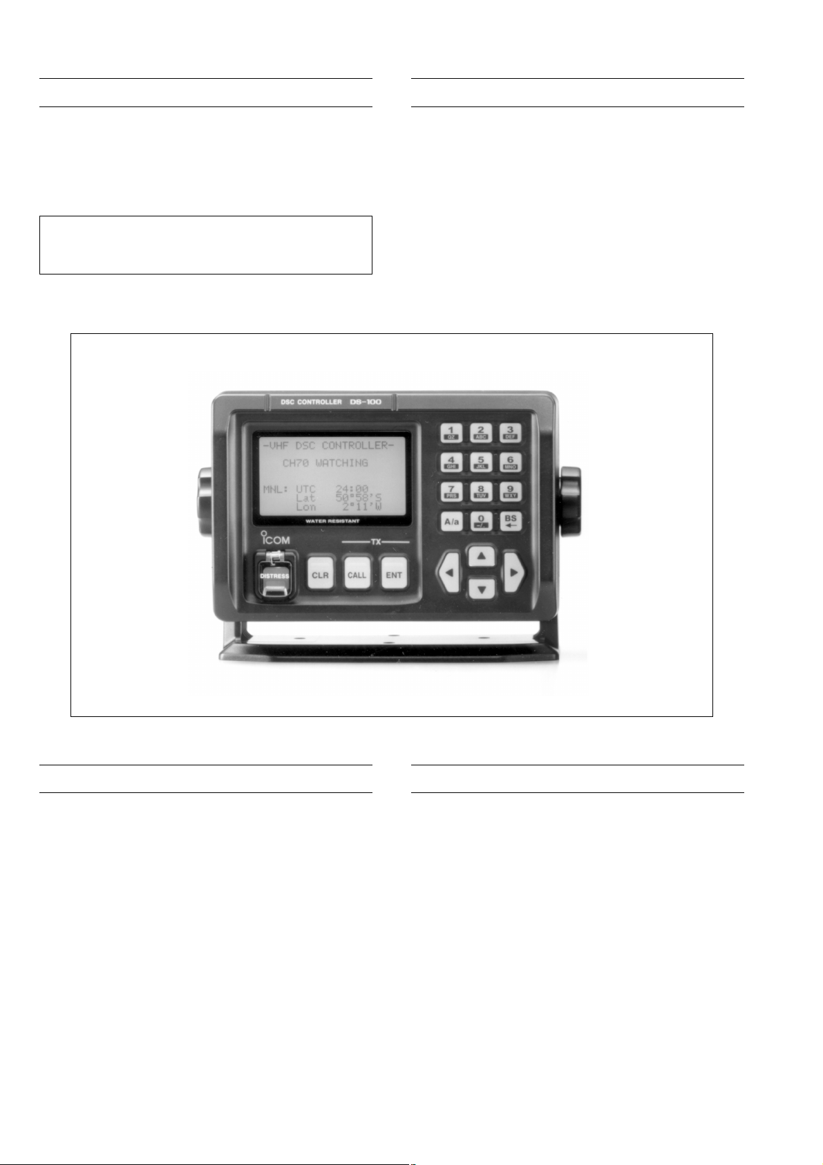
SECTION 2 INSIDE VIEWS
2 - 1
• MAIN UNIT
• LOGIC UNIT
Speaker
(SP1: PS1740P02)
FM IF IC
(IC1: TA31136FN)
2nd IF filter
(FI3: ALFY450E)
1st mixer
(Q2: 3SK166)
Crystal filter
(FI1, FI2: FL-310)
DSC decoder
(IC4: NJM2211M)
Reference Oscillator
(X2: CR-659 21.25 MHz)
LCD driver
IC6, IC7: HD61202UFS
IC8: HD61203UFS
VCO circuit
PLL IC
(IC2: µPD3140GS)
System clock
(X1: CR–610 7.9872 MHz)
CPU
(IC1: MB90F583BPFV-G)
Reset IC
(IC4: S-80928ANMP)
Inverter IC
(IC5: NJM2360M)
Page 6
SECTION 3 CIRCUIT DESCRIPTION
3 - 1
3-1 RECEIVER CIRCUITS
3-1-1 RF AMPLIFER CIRCUIT (MAIN UNIT)
The RF circuit amplifies signals within the range of frequency coverage and filters out-of-band signals.
The signals from the antenna connector are amplified at the
RF amplifier (Q1) via the bandpass filter (L1, C3). The amplified signals are applied to the 1st mixer circuit (Q2) after outof-band signals are suppressed at the 3-stage of bandpass
filters (L2, L3, L4, C11, C14, C17).
3-1-2 1ST MIXER AND 1ST IF CIRCUITS
(MAIN UNIT)
The 1st mixer circuit converts the received signal into a fixed
frequency of the 1st IF signal with a PLL output frequency.
By changing the PLL frequency, only the desired frequency
will pass through a crystal filter at the next stage of the 1st
mixer.
The signals from the RF circuit are mixed at the 1st mixer
(Q2) with a 1st LO signal coming from the PLL circuit to produce a 21.7 MHz 1st IF signal.
The 1st IF signal is applied to the crystal filters (FI1, FI2) to
suppress out-of-band signals. The filtered 1st IF signal is
amplified at the 1st IF amplifier (Q3), then applied to the 2nd
mixer circuit (IC1, pin 16).
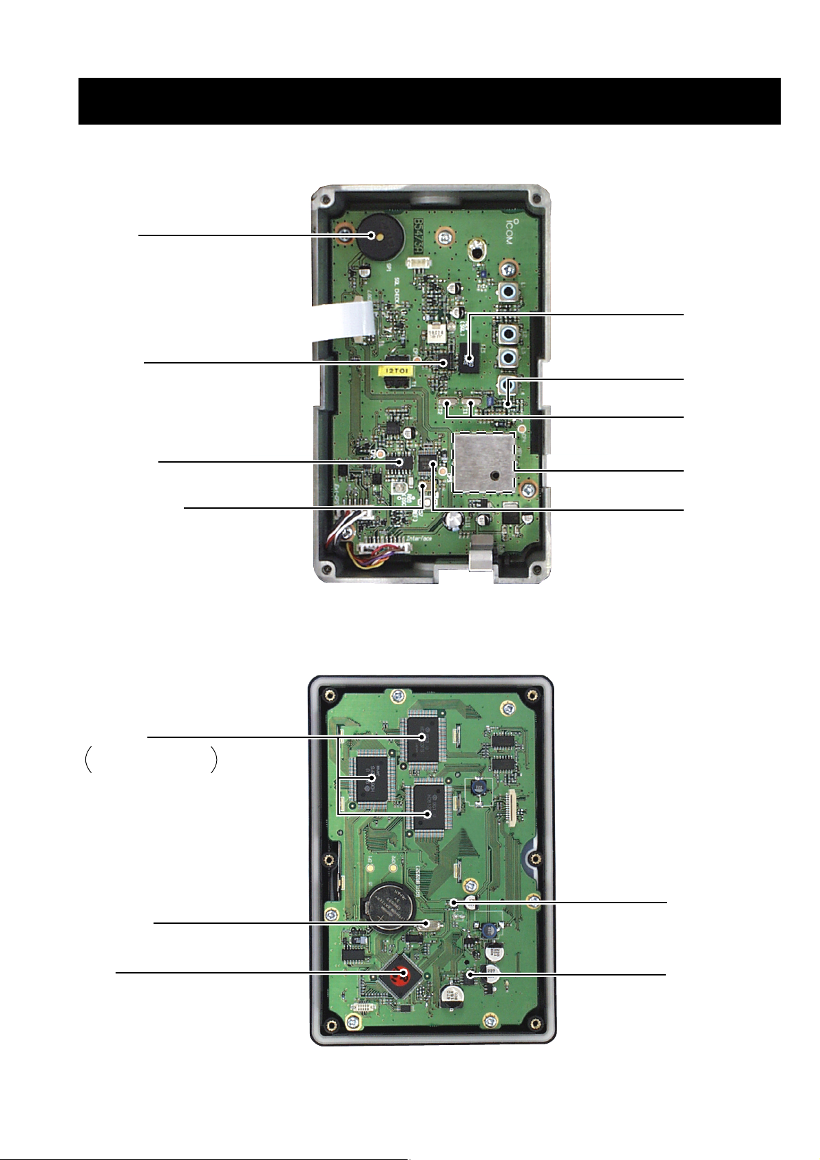
3-1-3 2ND IF AND DEMODULATOR CIRCUITS
(MAIN UNIT)
The 2nd mixer circuit converts the 1st IF signal into a 2nd IF
signal. Adouble conversion superheterodyne system (which
converts receive signals twice) improves the image rejection
ratio and obtains stable receiver gain.
The 1st IF signal from the IF amplifier is applied to the 2nd
mixer section of the FM IF IC (IC1, pin 16), and is mixed with
the 2nd LO signal to be converted into a 450 kHz 2nd IF signal.
The FM IF IC contains the 2nd mixer, limiter amplifier, quadrature detector and active filter circuits. A 2nd LO signal
(21.25 MHz) is produced at the PLL circuit using reference
frequency.
The 2nd IF signal from the 2nd mixer (IC1, pin 3) passes
through ceramic filter (FI3) to remove unwanted heterodyned frequencies. It is then amplified at the limiter amplifier (IC1, pin 5), and is applied to the quadrature detector
(IC1, pins 10, 11) to demodulate the 2nd IF signal into AF
signals.
3-1-4 SQUELCH CIRCUIT (MAIN UNIT)
A portion of the AF signals from the FM IF IC (IC1, pin 9) is
applied to the active filter section (IC1, pin 8) where noise
components are amplified and detected with an internal
noise detector. The squelch level adjustment pot (R29) is
connected to the active filter input (pin 8) to control the input
noise level.
The active filter section amplifies noise components. The filtered signals are rectified at the noise detector section and
converted into “SQL” signal (DC voltage) at the noise comparator section. The “SQL” signal is output from pin 13.
This squelch circuit is only used for the BUSY detection of
Ch70, and is not related the DSC decoder sensitivity and
etc.
• 2nd IF and demodulator circuits
Squelch level
adjustment pot
AF signal "DEMOD"
87 5 3
Noise
Active
filter
FM
detector
detector
Limiter
amp.
2nd IF filter
450 kHz
FI3
RSSI
Mixer
(21.25 MHz)
2
17
21.25 MHz
16
PLL IC
IC2
X2
IC1 TA31136FN
11109
X1
13
R8V
16
1st IF (21.7 MHz)
from Q3
"SQL" signal to the CPU
(LOGIC unit; IC1) pin 38
Page 7
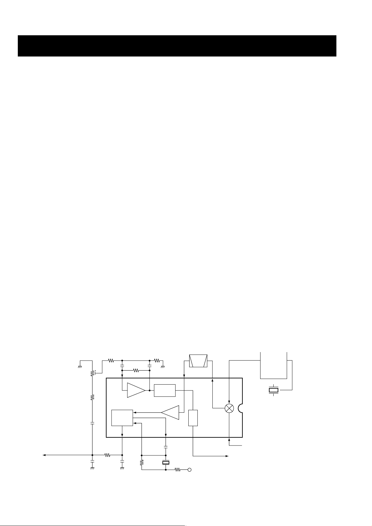
3 - 2
3-2 PLL CIRCUIT
3-2-1 PLL CIRCUIT (MAIN UNIT)
A PLL circuit provides stable oscillation of the receiver 1st
LO frequency. The PLL output compares the phase of the
divided VCO frequency to the reference frequency. The PLL
output frequency is controlled by the divided ratio (N-data) of
a programmable divider.
The PLL IC (IC2) contains a prescaler, programmable
counter, programmable divider phase detector, charge
pomp and etc. The entered signal is divided at the prescaler
and programmable counter section by the N-data ratio from
the CPU. The divided signal is detected on phase at the
phase detector using the reference frequency (21.25 MHz).
If the oscillated signal drifts, its phase changes from that of
the reference frequency, causing a lock voltage change to
compensate for the drift in the oscillated frequency.
3-3 DSC CIRCUITS
3-3-1 DSC DECODE CIRCUIT (MAIN UNIT)
The AF signals from FM IF IC (IC1, pin 9) are filtered at the
bandpass filter (IC3) with +18 dB/octave characteristics to
remove except 1300 Hz and 2100 Hz signals. The filtered
signals are converted analog signals into digital signals at
IC4, and are then applied to the CPU after shaping waveform at IC6.
3-3-2 DSC ENCODE CIRCUT (MAIN UNIT)
The DSC signals from the D/A outputs of CPU are amplified
at the buffer amplifier (Q17) and converted into 600 Ω
impedance at T1. The signals are output to the connected
transceiver as floating system output.
3-4 NMEA AND DATA INTERFACE
CIRCUITS
3-4-1 NMEA CIRCUIT (MAIN UNIT)
The NMEA signals (GGA) from OPC-945 are applied to IC5
and are shaped waveform at IC6, and are then applied to
the CPU.
3-4-2 DATA INTERFACE CIRCUIT (MAIN UNIT)
The control signals from the connected transceiver with
OPC-951 are applied to IC8 and are shaped wave form at
IC6, and are then applied to the CPU.
3-5 POWER SUPPLY CIRCUITS
3-5-1 VOLTAGE LINE (MAIN UNIT)
LINE
13.8 V
8 V
5 V
R8V
DESCRIPTION
The voltage from the connected transceiver.
Common 8 V converted from the 13.8 V line and
regulated by the 8 V regulator circuit (IC9).
Common 5 V converted from the 8 V line and
regulated by the 5 V regulator circuit (IC10).
8 V for receiver circuits regulated by the R8V
regulator circuit (Q15, Q16).
• PLL circuit
21.25 MHz signal
to the FM IF IC
Loop
filter
X2
21.25 MHz
Q5, D4, D5
IC2 (PLL IC)
8
17
VCO
Phase
detector
Programmable
divider
16
Buffer
Q6
Programmable
counter
Shift register
Prescaler
Buffer
Q8
Buffer
Q7
to 1st mixer circuit
2
3
PSTB
4
PCK
5
PDATA
Page 8
3 - 3
3-6 LOGIC CIRCUITS (LOGIC UNIT)
• CPU
IC1 is 16 bit single chip microcomputer and contains serial
I/O, timer, A/D converter, D/Aconverter, programmable I/O,
ROM and RAM.
• SYSTEM CLOCK CIRCUIT
X1 is a high-stability crystal oscillator and oscillated a
7.9872 MHz system clock for the CPU (IC1).
• RESET CIRCUIT
IC4 is a reset IC. When turn power ON, IC4 outputs a reset
signal (“LOW” pulse) to CPU (IC1, pin 75).
• LCD DRIVER
IC6–IC8 are LCD driver for a dot matrix LCD.
• INVERTER CIRCUIT
IC4 is a –8V DC-DC converter IC and converts –8 V from the
HV line. The converted voltage (–8V) is used for driving the
LCD.
• CLOCK CIRCUIT
IC3 is a clock IC and also used for backup the position/time
information for DSC.
• DIMMER CIRCUIT
Q2, Q3, Q6 are dimmer circuit and control the LCD backlight
(LED).
3-7 PORT ALLOCATIONS
3-7-1 CPU (LOGIC UNIT)
Outputs control signal for the LCD
contrast.
Input port for serial signal from the
NMEA connector (MAIN unit; J1) via
the photo coupler (MAIN unit; IC5)
and buffer amplifer (MAIN unit; IC6).
Outputs serial signal to the NMEA
connector (MAIN unit; J1) via the
buffer amplifier (Q13, Q14, D11).
Input port for noise level signal (DC
voltage) for squelch operation.
Output LCD backlight control signals
for the dimmer circuit (Q2, Q3, Q6).
Input port for the DSC decode signal.
Low : DSC signal is decoded.
Input port for the PLL unlock signal.
Low : While PLL is locked.
Outputs chip select signal for the LCD
drivers (IC6–IC8).
Output control signals for the LCD driver (IC6–IC8).
Input port for the control signal from
IC-M501EURO via the photo coupler
(MAIN unit; IC8) and buffer amplifier
(MAIN unit; IC6).
Outputs the control signal to ICM501EURO via the Buffer amplifier
(MAIN unit; Q11, Q12, D10).
Outputs busy LED (MAIN unit; DS1)
control signal.
Input port for the [ENT] key.
Input port for the [CLR] key.
Input port for the [CALL] key.
Input port for the [DISTRESS] key.
Outputs beep audio signal.
Outputs chip select signal for the clock
IC (IC3).
Outputs strobe signals for the PLL circuit.
Output data signals for the LCD driver
(IC6–IC8).
Outputs clock signal to the clock IC
(IC3).
Outputs serial signal for the clock IC
(IC3).
Input port for serial signal from the
clock IC (IC3).
Input port for the [1], [2] keys.
CADJ
NMEAI
NMEAO
SQL
DIM0–
DIM3
DDEC
UNLK
CS1,
CS2
RW,
DI, E
DATAS
DATAM
BUSY
KEY-ENT
KEY-CLR
KEY-CAL
KEY-DTR
BEEP
CCS
PSTB
DB0–
DB7
SCK
SO
SI
KEY-1,
KEY-2
31
36
37
38
41–44
45
46
52, 53
54,
55, 56
57
58
60
65
66
67
68
69
73
74
83–90
96
97
98
99, 100
1–7
8
10
11
12
13
14
15
19
20
23
24
26
30
KEY-3–
KEY-9
KEY-0
KEY-L
KEY-U
KEY-D
KEY-R
KEY-A
KEY-BS
CLRX
CLTX
ECK
EDA
RCEV
DSMOD
Input port for the [3]–[9] keys.
Input port for the [0] key.
Input port for the [LEFT] key.
Input port for the [UP] key.
Input port for the [DOWN] key.
Input port for the [RIGHT] key.
Input port for the [A/a] key.
Input port for the [BS] key.
Input port for the cloning data from the
buffer (MAIN unit; D8).
Output port for the cloning data to the
buffer (MAIN unit; Q9).
Outputs clock signal for EEPROM
(IC2).
Outputs serial data signal for EEP-
ROM (IC2).
Outputs the R8V regulator circuit
(MAIN unit; Q15, Q16) control signal.
High : While receiving
D/A output port for the DSC encode
signal to the buffer amplifier (MAIN
unit; Q17).
Pin Port
Description
number name
Pin Port
Description
number name
Page 9

EQUIPMENT GRADE AND RANGE EQUIPMENT GRADE AND RANGE
4-1 PREPARATION
■ REQUIRED TEST EQUIPMENT
4 - 1
SECTION 4 ADJUSTMENT PROCEDURES
DC power supply
Frequency counter
Standard signal
generator (SSG)
Distortion meter
Output voltage : 13.8 V DC
Current capacity : 2 Aor more
Frequency range : 0.1–300 MHz
Frequency accuracy: ±1 ppm or better
Sensitivity : 100 mV or better
Frequency range : 0.1–300 MHz
Output level : 0.1 µV–32 mV
(–127 to –17 dBm)
Frequency range : 1 kHz ±10 %
Measuring range : 1–100 %
Digital multimeter
DC voltmeter
AC millivoltmeter
Oscilloscope
External speaker
Terminator
Measuring range : 10 mV–10 V
Input impedance : 50 kΩ/V DC or bet-
ter
Measuring range : 10 mV–10 V
Frequency range : DC–20 MHz
Measuring range : 0.01–20 V
Input impedance : 4 Ω
Capacity : 5 W or more
Impedance : 100 kΩ
‘‘
CONNECTIONS
to the antenna connector
Standard signal
generator
–17 to –125 dBm
(32 mV to 0.13 µV)
DC power supply
13.8 V /15 A
+
–
to DC cable
Black Red
iM501EURODS-100
Page 10

4-2 REFERENCE AND RECEIVER ADJUSTMENTS
4 - 2
LOCK
VOLTAGE
REFERENCE
FREQUENCY
SENSITIVITY
SQUELCH
ADJUSTMENT
ADJUSTMENT ADJUSTMENT CONDITION
MEASUREMENT
VALUE
POINT
UNIT LOCATION UNIT ADJUST
1
1
1
1
• Receiving
• Receiving
• Connect an distortion meter with
an 100 kΩ dummy load to the
extenal speaker jack J4 on MAIN
unit.
• Connect an SSG to the antenna
connector and set as:
Frequency : 156.525 MHz
Level : 10 µV*
(–97 dBm)
Modulation : 1 kHz
Deviation : ±3.0 kHz
• Receiving
• Turn R29 counter clockwise on
the MAIN unit to 9 o’clock position.
• Connect an SSG to the antenna
connector and set as:
Frequency : 156.525 MHz
Level : 0.25 µV*
(–119 dBm)
Modulation : 1 kHz
Deviation : ±3.0 kHz
• Receiving
MAIN
MAIN
MAIN
MAIN
Connect a digital
multi-meter or oscilloscope to check
point CP3.
Connect a frequency counter to check
point CP4.
Connect a digital
multi-meter or oscilloscope to check
point CP1.
DS1
2.1 V
134.825000 MHz
Maximum voltage
At the point where the
check point DS1 just
turns OFF.
MAIN
MAIN
MAIN
MAIN
L9
C57
L1, L2,
L3, L4
Turn R29
to clockwise.
*This output level of a standard signal generator (SSG) is indicated as SSG’s open circuit.
Page 11

4 - 3
• MAIN unit
C57
Reference frequency
adjustment
L9
Lock voltage
adjustment
CP4
Reference frequency
check point
L4
Sensitivity
adjustment
L3
L2
L1
R29
Squelch
adjustment
CP3
Lock voltage
check point
CP1
Sensitivity
check point
DS1
Squelch
check point
J4
External SP
connector
Page 12

S.=Surface mount
IC1 1140008940 S.IC MB90F583BPFV-G
IC2 1130009680 S.IC HN58X2432TI
IC3 1130007450 S.IC RTC-4553A
IC4 1110004710 S.IC S-80928ANMP-DDR-T2
IC5 1110004200 S.IC NJM2360M-TE3
IC6 1130008850 S.IC HD61202UFS
IC7 1130008850 S.IC HD61202UFS
IC8 1130008860 S.IC HD61203UFS
IC9 1110003870 S.IC NJM2058M-T1
IC10 1110003870 S.IC NJM2058M-T1
Q2 1530002850 S.TRANSISTOR 2SC4116-BL (TE85R)
Q3 1520000460 S.TRANSISTOR 2SB1132 T100 R
Q4 1510000580 S.TRANSISTOR 2SA1362-GR (TE85R)
Q5 1590000420 S.TRANSISTOR RN1404 (TE85R)
Q6 1530002850 S.TRANSISTOR 2SC4116-BL (TE85R)
D1 1720000360 S.DIODE HSU88TRF
D2 1750000020 S.DIODE 1SS184 (TE85R)
D3 1790001470 S.DIODE SB10-05PCP-TD
D4 1790001010 S.ZENER MA8043-L (TX)
X1 6050010290 S.XTAL CR-610 (7.9872 MHz)
X2 6050011030 S.XTAL DMX-26S 32.768KHZ
L1 6200009370 S.COIL SLF7032T-221MR29-2
L2 6200008880 S.COIL SLF7032T-681MR16-2
R1 7030003280 S.RESISTOR ERJ3GEYJ 470 V (47 Ω)
R2 7030003280 S.RESISTOR ERJ3GEYJ 470 V (47 Ω)
R3 7030003280 S.RESISTOR ERJ3GEYJ 470 V (47 Ω)
R4 7030003280 S.RESISTOR ERJ3GEYJ 470 V (47 Ω)
R5 7410000990 S.ARRAY EXB-V8V 470JV
R9 7030003680 S.RESISTOR ERJ3GEYJ 104 V (100 kΩ)
R10 7030003680 S.RESISTOR ERJ3GEYJ 104 V (100 kΩ)
R11 7030003680 S.RESISTOR ERJ3GEYJ 104 V (100 kΩ)
R12 7030003680 S.RESISTOR ERJ3GEYJ 104 V (100 kΩ)
R13 7030003680 S.RESISTOR ERJ3GEYJ 104 V (100 kΩ)
R14 7030003680 S.RESISTOR ERJ3GEYJ 104 V (100 kΩ)
R15 7030003680 S.RESISTOR ERJ3GEYJ 104 V (100 kΩ)
R16 7030003680 S.RESISTOR ERJ3GEYJ 104 V (100 kΩ)
R17 7030003680 S.RESISTOR ERJ3GEYJ 104 V (100 kΩ)
R18 7030003680 S.RESISTOR ERJ3GEYJ 104 V (100 kΩ)
R19 7030003680 S.RESISTOR ERJ3GEYJ 104 V (100 kΩ)
R20 7030003680 S.RESISTOR ERJ3GEYJ 104 V (100 kΩ)
R21 7030003680 S.RESISTOR ERJ3GEYJ 104 V (100 kΩ)
R22 7030003680 S.RESISTOR ERJ3GEYJ 104 V (100 kΩ)
R23 7030003680 S.RESISTOR ERJ3GEYJ 104 V (100 kΩ)
R24 7030003680 S.RESISTOR ERJ3GEYJ 104 V (100 kΩ)
R25 7030003680 S.RESISTOR ERJ3GEYJ 104 V (100 kΩ)
R26 7030003680 S.RESISTOR ERJ3GEYJ 104 V (100 kΩ)
R27 7030003680 S.RESISTOR ERJ3GEYJ 104 V (100 kΩ)
R28 7030003680 S.RESISTOR ERJ3GEYJ 104 V (100 kΩ)
R29 7030003680 S.RESISTOR ERJ3GEYJ 104 V (100 kΩ)
R30 7030003680 S.RESISTOR ERJ3GEYJ 104 V (100 kΩ)
R31 7030003680 S.RESISTOR ERJ3GEYJ 104 V (100 kΩ)
R32 7030003630 S.RESISTOR ERJ3GEYJ 393 V (39 kΩ)
R33 7030003630 S.RESISTOR ERJ3GEYJ 393 V (39 kΩ)
R34 7030003560 S.RESISTOR ERJ3GEYJ 103 V (10 kΩ)
R35 7030004050 S.RESISTOR ERJ3GEYJ 1R0 V (1 Ω)
R36 7030004050 S.RESISTOR ERJ3GEYJ 1R0 V (1 Ω)
R37 7030006600 S.RESISTOR RR0816P-822-D (8.2 kΩ)
R38 7030006460 S.RESISTOR RR0816P-152-D (1.5 kΩ)
R39 7030003680 S.RESISTOR ERJ3GEYJ 104 V (100 kΩ)
R40 7030003680 S.RESISTOR ERJ3GEYJ 104 V (100 kΩ)
R41 7030003680 S.RESISTOR ERJ3GEYJ 104 V (100 kΩ)
R42 7030003680 S.RESISTOR ERJ3GEYJ 104 V (100 kΩ)
R43 7030003360 S.RESISTOR ERJ3GEYJ 221 V (220 Ω)
R44 7030003360 S.RESISTOR ERJ3GEYJ 221 V (220 Ω)
R45 7030003360 S.RESISTOR ERJ3GEYJ 221 V (220 Ω)
R46 7030003360 S.RESISTOR ERJ3GEYJ 221 V (220 Ω)
R47 7030003360 S.RESISTOR ERJ3GEYJ 221 V (220 Ω)
R48 7030003360 S.RESISTOR ERJ3GEYJ 221 V (220 Ω)
R49 7030003360 S.RESISTOR ERJ3GEYJ 221 V (220 Ω)
R50 7030003360 S.RESISTOR ERJ3GEYJ 221 V (220 Ω)
R51 7030003360 S.RESISTOR ERJ3GEYJ 221 V (220 Ω)
R52 7030003360 S.RESISTOR ERJ3GEYJ 221 V (220 Ω)
R53 7030003360 S.RESISTOR ERJ3GEYJ 221 V (220 Ω)
R54 7030003360 S.RESISTOR ERJ3GEYJ 221 V (220 Ω)
R55 7030003360 S.RESISTOR ERJ3GEYJ 221 V (220 Ω)
R56 7030003590 S.RESISTOR ERJ3GEYJ 183 V (18 kΩ)
R57 7030003360 S.RESISTOR ERJ3GEYJ 221 V (220 Ω)
R60 7030003220 S.RESISTOR ERJ3GEYJ 150 V (15 Ω)
R61 7030003220 S.RESISTOR ERJ3GEYJ 150 V (15 Ω)
R62 7030003220 S.RESISTOR ERJ3GEYJ 150 V (15 Ω)
R63 7030003220 S.RESISTOR ERJ3GEYJ 150 V (15 Ω)
R64 7030003220 S.RESISTOR ERJ3GEYJ 150 V (15 Ω)
R65 7030003220 S.RESISTOR ERJ3GEYJ 150 V (15 Ω)
R66 7030003500 S.RESISTOR ERJ3GEYJ 332 V (3.3 kΩ)
R67 7030003500 S.RESISTOR ERJ3GEYJ 332 V (3.3 kΩ)
R68 7030003580 S.RESISTOR ERJ3GEYJ 153 V (15 kΩ)
R69 7030003460 S.RESISTOR ERJ3GEYJ 152 V (1.5 kΩ)
R70 7030003500 S.RESISTOR ERJ3GEYJ 332 V (3.3 kΩ)
R71 7030003500 S.RESISTOR ERJ3GEYJ 332 V (3.3 kΩ)
R72 7030003560 S.RESISTOR ERJ3GEYJ 103 V (10 kΩ)
R73 7030003520 S.RESISTOR ERJ3GEYJ 472 V (4.7 kΩ)
R74 7510000900 S.THERMISTOR NTCCF2012 3SH 223KC-T
R75 7030003740 S.RESISTOR ERJ3GEYJ 334 V (330 kΩ)
R76 7030003790 S.RESISTOR ERJ3GEYJ 824 V (820 kΩ)
R77 7030003640 S.RESISTOR ERJ3GEYJ 473 V (47 kΩ)
R78 7030003840 S.RESISTOR ERJ3GEYJ 225 V (2.2 MΩ)
R79 7030003810 S.RESISTOR ERJ3GEYJ 125 V (1.2 MΩ)
R80 7030003650 S.RESISTOR ERJ3GEYJ 563 V (56 kΩ)
R81 7030003700 S.RESISTOR ERJ3GEYJ 154 V (150 kΩ)
R82 7030003680 S.RESISTOR ERJ3GEYJ 104 V (100 kΩ)
R83 7030003400 S.RESISTOR ERJ3GEYJ 471 V (470 Ω)
R84 7030003640 S.RESISTOR ERJ3GEYJ 473 V (47 kΩ)
R87 7030003560 S.RESISTOR ERJ3GEYJ 103 V (10 kΩ)
R88 7030003800 S.RESISTOR ERJ3GEYJ 105 V (1 MΩ)
R89 7030003640 S.RESISTOR ERJ3GEYJ 473 V (47 kΩ)
R90 7030003200 S.RESISTOR ERJ3GEYJ 100 V (10 Ω)
R91 7030003800 S.RESISTOR ERJ3GEYJ 105 V (1 MΩ)
R92 7030003750 S.RESISTOR ERJ3GEYJ 394 V (390 kΩ)
R93 7030003800 S.RESISTOR ERJ3GEYJ 105 V (1 MΩ)
R94 7030003680 S.RESISTOR ERJ3GEYJ 104 V (100 kΩ)
R95 7030003680 S.RESISTOR ERJ3GEYJ 104 V (100 kΩ)
R96 7030004120 S.RESISTOR ERJ3GEYJ 203 V (20 kΩ)
R97 7030003590 S.RESISTOR ERJ3GEYJ 183 V (18 kΩ)
R98 7030004120 S.RESISTOR ERJ3GEYJ 203 V (20 kΩ)
R99 7030003560 S.RESISTOR ERJ3GEYJ 103 V (10 kΩ)
R100 7030003560 S.RESISTOR ERJ3GEYJ 103 V (10 kΩ)
R101 7030003560 S.RESISTOR ERJ3GEYJ 103 V (10 kΩ)
R102 7030003440 S.RESISTOR ERJ3GEYJ 102 V (1 kΩ)
R103 7030003560 S.RESISTOR ERJ3GEYJ 103 V (10 kΩ)
R104 7030003630 S.RESISTOR ERJ3GEYJ 393 V (39 kΩ)
R105 7030003640 S.RESISTOR ERJ3GEYJ 473 V (47 kΩ)
R106 7030003560 S.RESISTOR ERJ3GEYJ 103 V (10 kΩ)
R107 7030003500 S.RESISTOR ERJ3GEYJ 332 V (3.3 kΩ)
C1 4030006860 S.CERAMIC C1608 JB 1H 102K-T-A
C2 4030006860 S.CERAMIC C1608 JB 1H 102K-T-A
C3 4030006860 S.CERAMIC C1608 JB 1H 102K-T-A
C4 4030008890 S.CERAMIC C1608 JB 1C 273K-T-A
C6 4030006860 S.CERAMIC C1608 JB 1H 102K-T-A
C7 4510006670 S.ELECTROLYTIC ECEV1CA471P
C8 4030006860 S.CERAMIC C1608 JB 1H 102K-T-A
C9 4510005370 S.ELECTROLYTIC ECEV1AA221P
C10 4030011280 S.CERAMIC C1608 CH 1H 271J-T-A
C11 4030006860 S.CERAMIC C1608 JB 1H 102K-T-A
C12 4510007120 S.ELECTROLYTIC ECEV1AA101SP
C13 4030006860 S.CERAMIC C1608 JB 1H 102K-T-A
C14 4030006860 S.CERAMIC C1608 JB 1H 102K-T-A
C15 4030006860 S.CERAMIC C1608 JB 1H 102K-T-A
C16 4030009650 S.CERAMIC C1608 CH 1H 240J-T-A
C17 4030009650 S.CERAMIC C1608 CH 1H 240J-T-A
C18 4030007070 S.CERAMIC C1608 CH 1H 330J-T-A
5 - 1
SECTION 5 PARTS LIST
REF ORDER
DESCRIPTION
NO. NO.
[LOGIC UNIT]
REF ORDER
DESCRIPTION
NO. NO.
[LOGIC UNIT]
Page 13

[MAIN UNIT][LOGIC UNIT]
S.=Surface mount
C19 4030007010 S.CERAMIC C1608 CH 1H 100D-T-A
C20 4030006860 S.CERAMIC C1608 JB 1H 102K-T-A
C21 4030006860 S.CERAMIC C1608 JB 1H 102K-T-A
C22 4030006860 S.CERAMIC C1608 JB 1H 102K-T-A
C23 4030006860 S.CERAMIC C1608 JB 1H 102K-T-A
C24 4030006860 S.CERAMIC C1608 JB 1H 102K-T-A
C25 4030006860 S.CERAMIC C1608 JB 1H 102K-T-A
C26 4030006860 S.CERAMIC C1608 JB 1H 102K-T-A
C27 4030006860 S.CERAMIC C1608 JB 1H 102K-T-A
C28 4030006860 S.CERAMIC C1608 JB 1H 102K-T-A
C29 4030009990 S.CERAMIC C1608 CH 1H 200J-T-A
C30 4030006860 S.CERAMIC C1608 JB 1H 102K-T-A
C31 4550006660 S.TANTALUM ECST1CC226R
C32 4510005370 S.ELECTROLYTIC ECEV1AA221P
C33 4030006860 S.CERAMIC C1608 JB 1H 102K-T-A
C34 4030006860 S.CERAMIC C1608 JB 1H 102K-T-A
J1 6510019500 S.CONNECTOR 52559-2290
J2 6510021300 S.CONNECTOR 52365-1091
J3 6510021860 CONNECTOR BH-800.8
DS1 5030001850 LCD TSD0402-UFFDCW
DS2 5040002310 S.LED SML-311YTT86
DS3 5040002310 S.LED SML-311YTT86
DS4 5040002310 S.LED SML-311YTT86
DS5 5040002310 S.LED SML-311YTT86
DS6 5040002310 S.LED SML-311YTT86
DS7 5040002310 S.LED SML-311YTT86
DS8 5040002310 S.LED SML-311YTT86
DS9 5040002310 S.LED SML-311YTT86
DS10 5040002310 S.LED SML-311YTT86
DS11 5040002310 S.LED SML-311YTT86
DS12 5040002310 S.LED SML-311YTT86
DS13 5040002310 S.LED SML-311YTT86
DS14 5040002310 S.LED SML-311YTT86
DS15 5040002310 S.LED SML-311YTT86
DS16 5040002310 S.LED SML-311YTT86
DS17 5040002310 S.LED SML-311YTT86
DS18 5040002310 S.LED SML-311YTT86
DS19 5040002310 S.LED SML-311YTT86
DS20 5040002310 S.LED SML-311YTT86
DS21 5040002310 S.LED SML-311YTT86
DS22 5040002310 S.LED SML-311YTT86
DS24 5040002310 S.LED SML-311YTT86
DS25 5040002310 S.LED SML-311YTT86
DS26 5040002310 S.LED SML-311YTT86
DS27 5040002310 S.LED SML-311YTT86
DS28 5040002310 S.LED SML-311YTT86
DS29 5040002310 S.LED SML-311YTT86
DS30 5040002310 S.LED SML-311YTT86
DS31 5040002310 S.LED SML-311YTT86
DS32 5040002310 S.LED SML-311YTT86
DS33 5040002310 S.LED SML-311YTT86
DS34 5040002310 S.LED SML-311YTT86
DS35 5040002310 S.LED SML-311YTT86
DS36 5040002310 S.LED SML-311YTT86
DS37 5040002310 S.LED SML-311YTT86
DS38 5040002310 S.LED SML-311YTT86
DS39 5040002310 S.LED SML-311YTT86
DS40 5040002310 S.LED SML-311YTT86
DS41 5040002310 S.LED SML-311YTT86
DS42 5040002310 S.LED SML-311YTT86
BT1 3020000020 LITHIUM CR2032
W1 8900006530 CABLE OPC-618
EP1 0910052953 PCB B 5475C
EP2 8930052541 LCD CONTACT SRCN-2349-SP-N-W-1
IC1 1110003200 S.IC TA31136FN (EL)
IC2 1130007610 S.IC µPD3140GS-E1 (DS8)
IC3 1110003750 S.IC M5218AFP 600C
IC4 1110003650 S.IC NJM2211M-TE1
IC5 1170000280 S.IC TLP121 (GB-TPL)
IC6 1130007420 S.IC TC7W14FU (TE12L)
IC8 1170000280 S.IC TLP121 (GB-TPL)
IC9 1110002030 IC TA7808S
IC10 1180001070 S.IC TA7805F (TE16L)
Q1 1580000700 S.FET 3SK292 (TE85R)
Q2 1580000490 S.FET 3SK166A-2-T7
Q3 1530002360 S.TRANSISTOR 2SC2714-Y (TE85R)
Q4 1530002850 S.TRANSISTOR 2SC4116-BL (TE85R)
Q5 1560000330 S.FET 2SK210-GR (TE85R)
Q6 1530002600 S.TRANSISTOR 2SC4215-O (TE85R)
Q7 1530002600 S.TRANSISTOR 2SC4215-O (TE85R)
Q8 1530002600 S.TRANSISTOR 2SC4215-O (TE85R)
Q9 1590000660 S.TRANSISTOR DTC144TU T107
Q11 1530002850 S.TRANSISTOR 2SC4116-BL (TE85R)
Q12 1590000660 S.TRANSISTOR DTC144TU T107
Q13 1530002850 S.TRANSISTOR 2SC4116-BL (TE85R)
Q14 1590000660 S.TRANSISTOR DTC144TU T107
Q15 1520000460 S.TRANSISTOR 2SB1132 T100 R
Q16 1590000660 S.TRANSISTOR DTC144TU T107
Q17 1530002850 S.TRANSISTOR 2SC4116-BL (TE85R)
Q18 1530002850 S.TRANSISTOR 2SC4116-BL (TE85R)
Q19 1530002850 S.TRANSISTOR 2SC4116-BL (TE85R)
Q20 1530002850 S.TRANSISTOR 2SC4116-BL (TE85R)
Q21 1530002850 S.TRANSISTOR 2SC4116-BL (TE85R)
Q22 1530002850 S.TRANSISTOR 2SC4116-BL (TE85R)
D2 1790001330 S.ZENER MA8036-L (TX)
D4 1790000640 S.VARICAP MA363B (TX)
D5 1790000640 S.VARICAP MA363B (TX)
D6 1750000550 S.DIODE 1SS355 TE-17
D8 1750000130 S.DIODE DA204U T107
D9 1750000550 S.DIODE 1SS355 TE-17
D10 1750000130 S.DIODE DA204U T107
D11 1750000130 S.DIODE DA204U T107
D12 1790000950 S.ZENER MA8056-M (TX)
D13 1790000950 S.ZENER MA8056-M (TX)
D14 1790000950 S.ZENER MA8056-M (TX)
FI1 2010002420 MONOLITH FL-310 (21R15AB)
FI2 2010002420 MONOLITH FL-310 (21R15AB)
FI3 2020001680 CERAMIC ALFY450E
X1 6070000210 S.DISCRIMINATOR CDBCA450CX24
X2 6050010800 S.XTAL CR-659 (21.25 MHz)
L1 6150003820 COIL LS-440
L2 6150003820 COIL LS-440
L3 6150003820 COIL LS-440
L4 6150003820 COIL LS-440
L5 6200003050 S.COIL NL 322522T-R82J-3
L6 6200004600 S.COIL MLF1608D R15K-T
L7 6200002410 S.COIL NL 252018T-056J
L8 6200003100 S.COIL NL 322522T-3R9J-3
L9 6130002360 S.COIL LB-257
L10 6200003090 S.COIL NL 322522T-2R7J-3
L11 6200004700 S.COIL MLR1608M R10K-T
L12 6200004700 S.COIL MLR1608M R10K-T
L13 6200004700 S.COIL MLR1608M R10K-T
L14 6200004920 S.COIL MLF1608A 2R2K-T
L15 6200002420 S.COIL NL 252018T-068J
R1 7030003670 S.RESISTOR ERJ3GEYJ 823 V (82 kΩ)
R3 7030003620 S.RESISTOR ERJ3GEYJ 333 V (33 kΩ)
R4 7030003600 S.RESISTOR ERJ3GEYJ 223 V (22 kΩ)
R5 7030003560 S.RESISTOR ERJ3GEYJ 103 V (10 kΩ)
R6 7030003640 S.RESISTOR ERJ3GEYJ 473 V (47 kΩ)
R7 7030003320 S.RESISTOR ERJ3GEYJ 101 V (100 Ω)
R8 7030003400 S.RESISTOR ERJ3GEYJ 471 V (470 Ω)
R9 7030003320 S.RESISTOR ERJ3GEYJ 101 V (100 Ω)
R12 7030003560 S.RESISTOR ERJ3GEYJ 103 V (10 kΩ)
5 - 2
REF ORDER
DESCRIPTION
NO. NO.
REF ORDER
DESCRIPTION
NO. NO.
Page 14

[MAIN UNIT][MAIN UNIT]
S.=Surface mount
R14 7030003200 S.RESISTOR ERJ3GEYJ 100 V (10 Ω)
R15 7030003480 S.RESISTOR ERJ3GEYJ 222 V (2.2 kΩ)
R16 7030003450 S.RESISTOR ERJ3GEYJ 122 V (1.2 kΩ)
R17 7030003460 S.RESISTOR ERJ3GEYJ 152 V (1.5 kΩ)
R18 7030003680 S.RESISTOR ERJ3GEYJ 104 V (100 kΩ)
R20 7030003320 S.RESISTOR ERJ3GEYJ 101 V (100 Ω)
R21 7030003560 S.RESISTOR ERJ3GEYJ 103 V (10 kΩ)
R22 7030003400 S.RESISTOR ERJ3GEYJ 471 V (470 Ω)
R23 7030003450 S.RESISTOR ERJ3GEYJ 122 V (1.2 kΩ)
R24 7030003460 S.RESISTOR ERJ3GEYJ 152 V (1.5 kΩ)
R25 7030003390 S.RESISTOR ERJ3GEYJ 391 V (390 Ω)
R26 7030003740 S.RESISTOR ERJ3GEYJ 334 V (330 kΩ)
R27 7030003460 S.RESISTOR ERJ3GEYJ 152 V (1.5 kΩ)
R28 7030003640 S.RESISTOR ERJ3GEYJ 473 V (47 kΩ)
R29 7310002740 S.TRIMMER RV-150 (RH03A3A14X0FC) 103
R30 7030003500 S.RESISTOR ERJ3GEYJ 332 V (3.3 kΩ)
R31 7030003280 S.RESISTOR ERJ3GEYJ 470 V (47 Ω)
R32 7030003380 S.RESISTOR ERJ3GEYJ 331 V (330 Ω)
R33 7410000950 S.ARRAY EXB-V8V 102JV
R34 7030003550 S.RESISTOR ERJ3GEYJ 822 V (8.2 kΩ)
R36 7030003410 S.RESISTOR ERJ3GEYJ 561 V (560 Ω)
R37 7030003320 S.RESISTOR ERJ3GEYJ 101 V (100 Ω)
R38 7030003300 S.RESISTOR ERJ3GEYJ 680 V (68 Ω)
R39 7030003320 S.RESISTOR ERJ3GEYJ 101 V (100 Ω)
R40 7030003480 S.RESISTOR ERJ3GEYJ 222 V (2.2 kΩ)
R41 7030003440 S.RESISTOR ERJ3GEYJ 102 V (1 kΩ)
R42 7030003440 S.RESISTOR ERJ3GEYJ 102 V (1 kΩ)
R43 7030003420 S.RESISTOR ERJ3GEYJ 681 V (680 Ω)
R44 7030003660 S.RESISTOR ERJ3GEYJ 683 V (68 kΩ)
R45 7030003420 S.RESISTOR ERJ3GEYJ 681 V (680 Ω)
R46 7030003660 S.RESISTOR ERJ3GEYJ 683 V (68 kΩ)
R47 7030003320 S.RESISTOR ERJ3GEYJ 101 V (100 Ω)
R48 7030003500 S.RESISTOR ERJ3GEYJ 332 V (3.3 kΩ)
R49 7030003480 S.RESISTOR ERJ3GEYJ 222 V (2.2 kΩ)
R50 7030003320 S.RESISTOR ERJ3GEYJ 101 V (100 Ω)
R51 7030003360 S.RESISTOR ERJ3GEYJ 221 V (220 Ω)
R52 7030003550 S.RESISTOR ERJ3GEYJ 822 V (8.2 kΩ)
R53 7030003460 S.RESISTOR ERJ3GEYJ 152 V (1.5 kΩ)
R54 7030003760 S.RESISTOR ERJ3GEYJ 474 V (470 kΩ)
R55 7030003760 S.RESISTOR ERJ3GEYJ 474 V (470 kΩ)
R56 7030003280 S.RESISTOR ERJ3GEYJ 470 V (47 Ω)
R57 7030003560 S.RESISTOR ERJ3GEYJ 103 V (10 kΩ)
R58 7030003560 S.RESISTOR ERJ3GEYJ 103 V (10 kΩ)
R59 7030003560 S.RESISTOR ERJ3GEYJ 103 V (10 kΩ)
R60 7030003760 S.RESISTOR ERJ3GEYJ 474 V (470 kΩ)
R61 7030003640 S.RESISTOR ERJ3GEYJ 473 V (47 kΩ)
R62 7030003380 S.RESISTOR ERJ3GEYJ 331 V (330 Ω)
R63 7030003680 S.RESISTOR ERJ3GEYJ 104 V (100 kΩ)
R64 7030003630 S.RESISTOR ERJ3GEYJ 393 V (39 kΩ)
R65 7030003580 S.RESISTOR ERJ3GEYJ 153 V (15 kΩ)
R66 7310002720 S.TRIMMER RV-148
(RH03A3AS3X0DA)
472
R67 7030003580 S.RESISTOR ERJ3GEYJ 153 V (15 kΩ)
R68 7030003440 S.RESISTOR ERJ3GEYJ 102 V (1 kΩ)
R69 7030003440 S.RESISTOR ERJ3GEYJ 102 V (1 kΩ)
R70 7030003280 S.RESISTOR ERJ3GEYJ 470 V (47 Ω)
R72 7030003540 S.RESISTOR ERJ3GEYJ 682 V (6.8 kΩ)
R73 7030003400 S.RESISTOR ERJ3GEYJ 471 V (470 Ω)
R74 7030003400 S.RESISTOR ERJ3GEYJ 471 V (470 Ω)
R75 7030003540 S.RESISTOR ERJ3GEYJ 682 V (6.8 kΩ)
R76 7030003680 S.RESISTOR ERJ3GEYJ 104 V (100 kΩ)
R77 7030003210 S.RESISTOR ERJ3GEYJ 120 V (12 Ω)
R78 7030003520 S.RESISTOR ERJ3GEYJ 472 V (4.7 kΩ)
R79 7030003610 S.RESISTOR ERJ3GEYJ 273 V (27 kΩ)
R80 7030003680 S.RESISTOR ERJ3GEYJ 104 V (100 kΩ)
R81 7030003610 S.RESISTOR ERJ3GEYJ 273 V (27 kΩ)
R82 7030003520 S.RESISTOR ERJ3GEYJ 472 V (4.7 kΩ)
R83 7030003210 S.RESISTOR ERJ3GEYJ 120 V (12 Ω)
R84 7030003560 S.RESISTOR ERJ3GEYJ 103 V (10 kΩ)
R85 7030003480 S.RESISTOR ERJ3GEYJ 222 V (2.2 kΩ)
R86 7030003280 S.RESISTOR ERJ3GEYJ 470 V (47 Ω)
R87 7030003280 S.RESISTOR ERJ3GEYJ 470 V (47 Ω)
R88 7030003280 S.RESISTOR ERJ3GEYJ 470 V (47 Ω)
R89 7410000990 S.ARRAY EXB-V8V 470JV
R90 7030003620 S.RESISTOR ERJ3GEYJ 333 V (33 kΩ)
R91 7030003320 S.RESISTOR ERJ3GEYJ 101 V (100 Ω)
R94 7030003410 S.RESISTOR ERJ3GEYJ 561 V (560 Ω)
R95 7030003320 S.RESISTOR ERJ3GEYJ 101 V (100 Ω)
R96 7030003320 S.RESISTOR ERJ3GEYJ 101 V (100 Ω)
R97 7030003550 S.RESISTOR ERJ3GEYJ 822 V (8.2 kΩ)
R98 7030003550 S.RESISTOR ERJ3GEYJ 822 V (8.2 kΩ)
R99 7030003770 S.RESISTOR ERJ3GEYJ 564 V (560 kΩ)
R100 7030003710 S.RESISTOR ERJ3GEYJ 184 V (180 kΩ)
R101 7030003490 S.RESISTOR ERJ3GEYJ 272 V (2.7 kΩ)
R102 7030003380 S.RESISTOR ERJ3GEYJ 331 V (330 Ω)
R103 7030003620 S.RESISTOR ERJ3GEYJ 333 V (33 kΩ)
R104 7030003620 S.RESISTOR ERJ3GEYJ 333 V (33 kΩ)
R105 7030003480 S.RESISTOR ERJ3GEYJ 222 V (2.2 kΩ)
R106 7030003680 S.RESISTOR ERJ3GEYJ 104 V (100 kΩ)
R107 7030003290 S.RESISTOR ERJ3GEYJ 560 V (56 Ω)
R108 7030003520 S.RESISTOR ERJ3GEYJ 472 V (4.7 kΩ)
R109 7030003520 S.RESISTOR ERJ3GEYJ 472 V (4.7 kΩ)
R111 7030003560 S.RESISTOR ERJ3GEYJ 103 V (10 kΩ)
R112 7030003560 S.RESISTOR ERJ3GEYJ 103 V (10 kΩ)
R113 7030003560 S.RESISTOR ERJ3GEYJ 103 V (10 kΩ)
R114 7030003440 S.RESISTOR ERJ3GEYJ 102 V (1 kΩ)
R115 7030003670 S.RESISTOR ERJ3GEYJ 823 V (82 kΩ)
R116 7030003580 S.RESISTOR ERJ3GEYJ 153 V (15 kΩ)
R117 7030003440 S.RESISTOR ERJ3GEYJ 102 V (1 kΩ)
R118 7030003330 S.RESISTOR ERJ3GEYJ 121 V (120 Ω)
R119 7030003680 S.RESISTOR ERJ3GEYJ 104 V (100 kΩ)
R120 7030003520 S.RESISTOR ERJ3GEYJ 472 V (4.7 kΩ)
R121 7030003200 S.RESISTOR ERJ3GEYJ 100 V (10 Ω)
R123 7030003620 S.RESISTOR ERJ3GEYJ 333 V (33 kΩ)
C1 4030006990 S.CERAMIC C1608 CH 1H 080D-T-A
C2 4030006990 S.CERAMIC C1608 CH 1H 080D-T-A
C3 4030006980 S.CERAMIC C1608 CH 1H 070D-T-A
C4 4030009510 S.CERAMIC C1608 CH 1H 010B-T-A
C5 4030006860 S.CERAMIC C1608 JB 1H 102K-T-A
C6 4030007170 S.CERAMIC C1608 CH 1H 221J-T-A
C7 4030006860 S.CERAMIC C1608 JB 1H 102K-T-A
C8 4030006850 S.CERAMIC C1608 JB 1H 471K-T-A
C9 4030006860 S.CERAMIC C1608 JB 1H 102K-T-A
C10 4030006850 S.CERAMIC C1608 JB 1H 471K-T-A
C11 4030006990 S.CERAMIC C1608 CH 1H 080D-T-A
C12 4030006970 S.CERAMIC C1608 CH 1H 060D-T-A
C13 4030006970 S.CERAMIC C1608 CH 1H 060D-T-A
C14 4030006980 S.CERAMIC C1608 CH 1H 070D-T-A
C15 4030009500 S.CERAMIC C1608 CH 1H 0R5B-T-A
C16 4030009500 S.CERAMIC C1608 CH 1H 0R5B-T-A
C17 4030006990 S.CERAMIC C1608 CH 1H 080D-T-A
C18 4030006900 S.CERAMIC C1608 JB 1E 103K-T-A
C19 4030006860 S.CERAMIC C1608 JB 1H 102K-T-A
C20 4030009920 S.CERAMIC C1608 CH 1H 050B-T-A
C21 4030006860 S.CERAMIC C1608 JB 1H 102K-T-A
C22 4030007110 S.CERAMIC C1608 CH 1H 680J-T-A
C23 4030006860 S.CERAMIC C1608 JB 1H 102K-T-A
C25 4030011770 S.CERAMIC C1608 CH 1H 060B-T-A
C27 4030006860 S.CERAMIC C1608 JB 1H 102K-T-A
C28 4030006900 S.CERAMIC C1608 JB 1E 103K-T-A
C29 4030008880 S.CERAMIC C1608 JB 1C 223K-T-A
C30 4030006860 S.CERAMIC C1608 JB 1H 102K-T-A
C31 4030006900 S.CERAMIC C1608 JB 1E 103K-T-A
C32 4030008880 S.CERAMIC C1608 JB 1C 223K-T-A
C33 4030006860 S.CERAMIC C1608 JB 1H 102K-T-A
C34 4030006860 S.CERAMIC C1608 JB 1H 102K-T-A
C36 4030006860 S.CERAMIC C1608 JB 1H 102K-T-A
C37 4030007080 S.CERAMIC C1608 CH 1H 390J-T-A
C38 4030007080 S.CERAMIC C1608 CH 1H 390J-T-A
C39 4030006860 S.CERAMIC C1608 JB 1H 102K-T-A
C40 4030011600 S.CERAMIC C1608 JB 1C 104KT-N
C41 4030007130 S.CERAMIC C1608 CH 1H 101J-T-A
C42 4030006860 S.CERAMIC C1608 JB 1H 102K-T-A
C43 4030006860 S.CERAMIC C1608 JB 1H 102K-T-A
C44 4030011600 S.CERAMIC C1608 JB 1C 104KT-N
C45 4030007090 S.CERAMIC C1608 CH 1H 470J-T-A
C46 4030011600 S.CERAMIC C1608 JB 1C 104KT-N
C47 4510004630 S.ELECTROLYTIC ECEV1CA100SR
C48 4030006900 S.CERAMIC C1608 JB 1E 103K-T-A
C49 4030006860 S.CERAMIC C1608 JB 1H 102K-T-A
C50 4030011600 S.CERAMIC C1608 JB 1C 104KT-N
C51 4030006860 S.CERAMIC C1608 JB 1H 102K-T-A
C52 4030006900 S.CERAMIC C1608 JB 1E 103K-T-A
C53 4030012600 S.CERAMIC C2012 JB 1A 105M-T-A
C54 4030007160 S.CERAMIC C1608 CH 1H 181J-T-A
C55 4030007160 S.CERAMIC C1608 CH 1H 181J-T-A
C56 4030007040 S.CERAMIC C1608 CH 1H 180J-T-A
C57 4610002150 S.TRIMMER CTZ3S-10A-W1-AF
C58 4030007020 S.CERAMIC C1608 CH 1H 120J-T-A
C59 4030011600 S.CERAMIC C1608 JB 1C 104KT-N
C60 4030006900 S.CERAMIC C1608 JB 1E 103K-T-A
C61 4030006860 S.CERAMIC C1608 JB 1H 102K-T-A
C62 4030008880 S.CERAMIC C1608 JB 1C 223K-T-A
5 - 3
REF ORDER
DESCRIPTION
NO. NO.
REF ORDER
DESCRIPTION
NO. NO.
Page 15

[MAIN UNIT][MAIN UNIT]
S.=Surface mount
C63 4030006900 S.CERAMIC C1608 JB 1E 103K-T-A
C64 4550006170 S.TANTALUM ECST1AY225R
C66 4030006860 S.CERAMIC C1608 JB 1H 102K-T-A
C67 4030011600 S.CERAMIC C1608 JB 1C 104KT-N
C68 4030012600 S.CERAMIC C2012 JB 1A 105M-T-A
C69 4030006850 S.CERAMIC C1608 JB 1H 471K-T-A
C70 4550000530 S.TANTALUM TESVA 1V 104M1-8L
C72 4030009520 S.CERAMIC C1608 CH 1H 020B-T-A
C73 4030009520 S.CERAMIC C1608 CH 1H 020B-T-A
C74 4030009910 S.CERAMIC C1608 CH 1H 040B-T-A
C75 4030009560 S.CERAMIC C1608 CH 1H R75B-T-A
C76 4030006860 S.CERAMIC C1608 JB 1H 102K-T-A
C77 4030006900 S.CERAMIC C1608 JB 1E 103K-T-A
C78 4030009990 S.CERAMIC C1608 CH 1H 200J-T-A
C79 4030006860 S.CERAMIC C1608 JB 1H 102K-T-A
C80 4030009920 S.CERAMIC C1608 CH 1H 050B-T-A
C81 4030007020 S.CERAMIC C1608 CH 1H 120J-T-A
C82 4030006860 S.CERAMIC C1608 JB 1H 102K-T-A
C83 4030007020 S.CERAMIC C1608 CH 1H 120J-T-A
C84 4030006860 S.CERAMIC C1608 JB 1H 102K-T-A
C85 4030006900 S.CERAMIC C1608 JB 1E 103K-T-A
C86 4030006900 S.CERAMIC C1608 JB 1E 103K-T-A
C87 4030008850 S.CERAMIC C1608 JB 1C 123K-T-A
C88 4030008900 S.CERAMIC C1608 JB 1C 333K-T-A
C89 4030008900 S.CERAMIC C1608 JB 1C 333K-T-A
C90 4030006850 S.CERAMIC C1608 JB 1H 471K-T-A
C91 4030008920 S.CERAMIC C1608 JB 1C 473K-T-A
C92 4030011810 S.CERAMIC C1608 JB 1A 224K-T-N
C93 4030011600 S.CERAMIC C1608 JB 1C 104KT-N
C94 4030011600 S.CERAMIC C1608 JB 1C 104KT-N
C95 4510004630 S.ELECTROLYTIC ECEV1CA100SR
C96 4030011600 S.CERAMIC C1608 JB 1C 104KT-N
C97 4340000020 S.MYLAR ECWU 1C 333JB5
C98 4030011600 S.CERAMIC C1608 JB 1C 104KT-N
C99 4030006870 S.CERAMIC C1608 JB 1H 222K-T-A
C100 4030006900 S.CERAMIC C1608 JB 1E 103K-T-A
C101 4030006880 S.CERAMIC C1608 JB 1H 472K-T-A
C102 4030011600 S.CERAMIC C1608 JB 1C 104KT-N
C103 4030011600 S.CERAMIC C1608 JB 1C 104KT-N
C104 4030006850 S.CERAMIC C1608 JB 1H 471K-T-A
C106 4030006880 S.CERAMIC C1608 JB 1H 472K-T-A
C107 4030011600 S.CERAMIC C1608 JB 1C 104KT-N
C108 4030007090 S.CERAMIC C1608 CH 1H 470J-T-A
C109 4030006860 S.CERAMIC C1608 JB 1H 102K-T-A
C110 4030006900 S.CERAMIC C1608 JB 1E 103K-T-A
C111 4510004590 ELECTROLYTIC 16 MV 470 HC
C112 4030006900 S.CERAMIC C1608 JB 1E 103K-T-A
C113 4030011600 S.CERAMIC C1608 JB 1C 104KT-N
C114 4030011600 S.CERAMIC C1608 JB 1C 104KT-N
C115 4510004630 S.ELECTROLYTIC ECEV1CA100SR
C116 4030006900 S.CERAMIC C1608 JB 1E 103K-T-A
C117 4030011600 S.CERAMIC C1608 JB 1C 104KT-N
C118 4030011600 S.CERAMIC C1608 JB 1C 104KT-N
C119 4510004630 S.ELECTROLYTIC ECEV1CA100SR
C120 4030006860 S.CERAMIC C1608 JB 1H 102K-T-A
C121 4030007090 S.CERAMIC C1608 CH 1H 470J-T-A
C123 4030011600 S.CERAMIC C1608 JB 1C 104KT-N
C124 4550006150 S.TANTALUM ECST1CY105R
C126 4030011600 S.CERAMIC C1608 JB 1C 104KT-N
C127 4030011600 S.CERAMIC C1608 JB 1C 104KT-N
C130 4030012600 S.CERAMIC C2012 JB 1A 105M-T-A
C131 4550006130 S.TANTALUM ECST1VY224R
C132 4030008890 S.CERAMIC C1608 JB 1C 273K-T-A
C133 4030008890 S.CERAMIC C1608 JB 1C 273K-T-A
C134 4030006870 S.CERAMIC C1608 JB 1H 222K-T-A
C135 4030009490 S.CERAMIC C1608 JB 1H 821K-T-A
C136 4510004630 S.ELECTROLYTIC ECEV1CA100SR
C137 4030011600 S.CERAMIC C1608 JB 1C 104KT-N
C138 4030006860 S.CERAMIC C1608 JB 1H 102K-T-A
C139 4030006860 S.CERAMIC C1608 JB 1H 102K-T-A
C140 4510004630 S.ELECTROLYTIC ECEV1CA100SR
C141 4030006860 S.CERAMIC C1608 JB 1H 102K-T-A
C142 4030006900 S.CERAMIC C1608 JB 1E 103K-T-A
C143 4030006900 S.CERAMIC C1608 JB 1E 103K-T-A
C144 4030006860 S.CERAMIC C1608 JB 1H 102K-T-A
C145 4030007030 S.CERAMIC C1608 CH 1H 150J-T-A
C146 4030007030 S.CERAMIC C1608 CH 1H 150J-T-A
C147 4030006860 S.CERAMIC C1608 JB 1H 102K-T-A
C148 4030006860 S.CERAMIC C1608 JB 1H 102K-T-A
C149 4030011600 S.CERAMIC C1608 JB 1C 104KT-N
C150 4030006860 S.CERAMIC C1608 JB 1H 102K-T-A
C151 4030006900 S.CERAMIC C1608 JB 1E 103K-T-A
C152 4030006860 S.CERAMIC C1608 JB 1H 102K-T-A
C153 4030006860 S.CERAMIC C1608 JB 1H 102K-T-A
C154 4550006830 S.TANTALUM ECST1DY475R
C155 4030009490 S.CERAMIC C1608 JB 1H 821K-T-A
C156 4030006870 S.CERAMIC C1608 JB 1H 222K-T-A
C157 4510004630 S.ELECTROLYTIC ECEV1CA100SR
J1 6510022310 S.CONNECTOR B5B-PH-SM3-TB
J2 6510022030 S.CONNECTOR B10B-ZR-SM3-TF
J3 6510019500 S.CONNECTOR 52559-2290
J4 6510003380 S.CONNECTOR B02B-EH-S
DS1 5040002310 S.LED SML-311YTT86
T1 5920000570 TRANSFORMER 12T01
SP1 2520000110 PIEZO BUZZER PS1740P02
EP1 0910052942 PCB B 5473B
5 - 4
REF ORDER
DESCRIPTION
NO. NO.
REF ORDER
DESCRIPTION
NO. NO.
Page 16

J1 6510004880 Connector MR-DS-E 01 1
W1 8900009740 Cable OPC-945 1
W2 8900009690 Cable OPC-951 1
EP1 6910011940 Bead ZCAT2436-1330A-M 1
MP3 8410002340 2349 heatsink 1
MP4 8210017200 2349 front panel assembly 1
MP5 8210017150 2345 rear panel assembly 1
MP6 8930052060 2345 F-packing 1
MP7 8930052050 2345 R-packing 1
MP16 8930052430 2345 A-IC crip 1
MP18 8810008660 Screw PH BT M3 × 8 NI-ZU 5
MP19 8810008660 Screw PH BT M3 × 8 NI-ZU 7
MP20 8810004540 Screw M3 × 8 SUS 6
MP21 8810006050 Icom screw E7 6
MP22 8930052290 O ring (AD) 6
MP23 8850000690 Flat washer M3 (3×7×0.5) SUS 6
MP25 8810004540 Screw M3 × 8 SUS 2
MP26 8930034300 1542 ANT seal 1
MP27 8930049320 2288 VENT. sheet 1
REF. NO.
SECTION 6 MECHANICAL PARTS
[CHASSIS PARTS]
ORDER NO. DESCRIPTION QTY.
MP1 8610010560 2040 knob bolt (black) 2
MP2 8010018151 2345 mobile bracket-1 1
MP3 8850000500 Spring washer M5 SUS 2
MP4 8810001490 Screw PH A M5 × 20 SUS 2
MP5 8850000180 Flat washer M5 SUS 2
[UNPACKING]
REF. NO. ORDER NO. DESCRIPTION QTY.
6 - 1
REF. NO.
SP1 2520000110 Piezo buzzer PS1740P02 1
MP1 8510012590 2289 VCO case 1
[MAIN UNIT]
ORDER NO. DESCRIPTION QTY.
J3 6510021860 Connector BH-800.8 1
BT1 3020000110 Lithium CR2032 1
DS1 5030001850 LCD TSD0402-UFFDCW 1
EP2 8930052541 LCD contact SRCN-2349-SP-N-W-1 2
MP1 8210016790 2349 reflector 1
MP2 8930051950 2349 LCD holder 1
MP3 8930052530 2349 LCD filter 1
[LOGIC UNIT]
REF. NO. ORDER NO. DESCRIPTION QTY.
Screw abbreviations PH: Pan head BT: Self-Tapping
SUS: Stainless NI-ZU: Nickel-zinc
Page 17

6 - 2
MAIN UNIT
LOGIC UNIT
MP7 (CH)
MP21 (CH)
MP23 (CH)
MP22 (CH)
MP20 (CH)
MP19 (CH)
MP4 (CH)
MP6 (CH)
MP2 (L)
DS1 (L)
EP2 (L)
MP18 (CH)
MP16 (CH)
MP1 (M)
J3 (L)
+
BT1 (L)
MP3 (L)
MP1 (L)
MP5 (CH)
W2 (CH)
EP1 (CH)
W2 (CH)
SP1 (M)
MP25 (CH)
MP3 (CH)
J1 (CH)
W1 (CH)
MP26 (CH)
Unit abbreviations (CH): CHASSIS PARTS
(M): MAIN UNIT
(L): LOGIC UNIT
Page 18

7 - 1
SECTION 7 SEMI-CONDUCTOR INFORMATION
• TRANSISTORS AND FET’S
2SA1362 GR 2SB1132 T100 R 2SC2714 Y 2SC4116 BL 2SC4215 O
2SK210 GR 3SK166A-2-T7 3SK292 DTC144 TU T107 RN1404
(Symbol: AEG) (Symbol: BAR) (Symbol: QY) (Symbol: LL) (Symbol: QO)
(Symbol: YG) (Symbol: K) (Symbol: UK) (Symbol: 06) (Symbol: XD)
B
E
C
B
C
E
B
E
C
B
E
C
B
E
C
D
G
S
D
S
G2
G1
D
S
G2
G1
B
E
C
B
E
C
• DIODES
1SS184 1SS355 DA204 U T107 HSU88TRF MA363 B
MA8036 L MA8043 L MA8056 M SB10 05PCP TD
(Symbol: B3) (Symbol: A) (Symbol: K) (Symbol: 9) (Symbol: 6D)
(Symbol: 3_6) (Symbol: 4_3) (Symbol: 5-6) (Symbol: SA)
C
A1
A2
A
C
A
C
Page 19

8 - 1
8-1 LOGIC UNIT
SECTION 8 BOARD LAYOUTS
• TOP VIEW
Page 20

8 - 2
• BOTTOM VIEW
1
7
14
8
1
25
26
1
4
85
50
14
58
51
75
76
100
80 51
30
30 1
51 80
81
100
50
31
1
100
81
31
50
30 1
51 80
81
100
50
31
1
7
1481
7
14
8
BEEP
8V
GND
5V
DATAM
NMEAI
DSMOD
SQL
CLRX
UNLK
PCK
Vcc
BUSY
GND
DATAS
NMEAO
GND
DDEC
RCEV
CLTX
PDATA
PSTB
1
2
21
22
to MAIN unit J3
J1
Page 21

8 - 3
8-2 MAIN UNIT
• TOP VIEW
1
5
to OPC-945
J1
NMEAI+
NMEAI–
NMEAO+
ICF3
GND
to OPC-951
1
10
J2
GND
Vcc
DSC–
DSC+
DATAM+
DATAM–
DATAS+
DATAS–
ICF3
GND
to LOGIC unit J1
1
2
21
22
J3
BEEP
8V
GND
5V
DATAM
NMEAI
DSMOD
SQL
CLRX
UNLK
PCK
Vcc
BUSY
GND
DATAS
NMEAO
GND
DDEC
RCEV
CLTX
PDATA
PSTB
18
16
45
81
1
1
4
8
5
1
10
20
11
7
14
8
9
Page 22

9 - 1
SECTION 9 BLOCK DIAGRAM
ANT
CH70
FI3
FM IF IC
Q18, Q19
2SC4116
IC4
NJM2211M
DSC
DECODER
SQL
IC3
M5218AFP
X2 CR-659
(21.25MHz)
IC1
TA31136FN
IC2
µPD3140GS
Q3
2SC2714
Q7
2SC4215
FI1, FI2
FL-310
3stage
5V
Q2
3SK166
1stage
Q1
3SK292
IC10
TA7805F
8V
Vcc
IC9
TA7808S
Q15 2SB1132
Q16 DTC144TU
R8V
RCEV
Q6
2SC4215
VCO
Q8
2SC4215
Q5 2SK210
D4, D5 MA363B
PLL DATA BUS
MAIN unit
LOGIC unit
IC2
HN58X2432TI
EEPROM
RESET
DIM
CTRL
X1 CR-610
X2 DMX-26S
DSC
(Port)
NMEAI
IC1
MB90F583BPFV-G
Q17
2SC4116
IC6
TC7W14FU
NMEAI+
NMEAI–
DSC+
DSC–
IC5
TLP121
PHOTO
COUPLER
PHOTO
COUPLER
DATAS+
DATAS–
NMEAO+
NMEAO–
ICF3
IC8
TLP121
Q13 2SC4116
Q14 DTC144TU
D11 DA204U
IC6
TC7W14FU
Q9 DTC144TU
D8 DA204U
NMEAO
DATAS
DATAM
CLTX
CLRX
CPU
KEY
CLOCK
IC4
S-80928ANMP
IC3
RTC-4553A
DS1
TSD0402
IC6, IC7 HD61202UFS
IC8 HD61203UFS
Q11 2SC4116
Q12 DTC144TU
D10 DA204U
DATAM+
DATAM–
DISTRESS SW
BEEP
SP1
Q2, Q6 2SC4116
Q3 2SB1132
LED
Page 23

10 - 1
10-1 LOGIC UNIT
SECTION 10 VOLTAGE DIAGRAM
S2 S3
KEY-9
KEY-6
KEY-3
KEY-0
KEY-8
KEY-5
KEY-2
KEY-A
KEY-7
KEY-4
KEY-1
S1
R9 100k
R10 100k
R12 100k
R13 100k
R14 100k
R15 100k
R16 100k
R17 100k
R18 100k
R19 100k
R20 100k
R21 100k
R22 100k
R23 100k
R24 100k
R25 100k
R26 100k
R27 100k
R28 100k
R11 100k
DS16DS15DS14 DS27
R47
220
DS4DS3DS2
R43
220
LCD BACKLIGHT
X221X212X203X194X185X176X167X158X149X1310X1211X1112X10
13X914X815X716X617X518X419X320X221X122
VEE
23
V6L24V5L25V2L26V1L
27
VCC
28DL29FS30
X4380X4479X4578X4677X4776X4875X4974X5073X5172X5271X5370X5469X5568X5667X5766X5865X5964X6063X6162X6261X6360X6459VEE
58
V6R57V5R56V2R55V1R
54TH53
CL252CL1
51
IC8
HD61203UFS
COM22
COM21
COM20
COM19
COM18
COM17
COM16
COM15
COM23
COM24
COM25
COM26
COM27
COM28
COM29
COM30
COM31
COM32
COM33
COM34
COM35
COM36
COM37
COM38
COM39
COM40
COM41
COM42
100
99
98
97
96
95
94
93
92
91
90
89
88
87
86
85
84
83
82
81
X23
X24
X25
X26
X27
X28
X29
X30
X31
X32
X33
X34
X35
X36
X37
X38
X39
X40
X41
X42
DS1
DS2
C
NC
R
NC
CR
STB
SHL
GND
NC
MS
FAI1
FAI2
NC
FRM
M
NC
FCS
DR
31
32
33
34
35
36
37
38
39
40
41
42
43
44
45
46
47
48
49
50
DS1
TSD0402
SEG11
2345678910111213141516171819202122232425262728293031323334353637383940414243444546474849505152535455565758596061626364
65666768697071727374757677787980818283848586878889909192939495
96
SEG2
SEG3
SEG4
SEG5
SEG6
SEG7
SEG8
SEG9
SEG10
SEG11
SEG12
SEG13
SEG14
SEG15
SEG16
SEG17
SEG18
SEG19
SEG20
SEG21
SEG22
SEG23
SEG24
SEG25
SEG26
SEG27
SEG28
SEG29
SEG30
SEG31
SEG32
SEG33
SEG34
SEG35
SEG36
SEG37
SEG38
SEG39
SEG40
SEG41
SEG42
SEG43
SEG44
SEG45
SEG46
SEG47
SEG48
SEG49
SEG50
SEG51
SEG52
SEG53
SEG54
SEG55
SEG56
SEG57
SEG58
SEG59
SEG60
SEG61
SEG62
SEG63
SEG64
COM1
COM2
COM3
COM4
COM5
COM6
COM7
COM8
COM9
COM10
COM11
COM12
COM13
COM14
COM15
COM16
COM17
COM18
COM19
COM20
COM21
COM22
COM23
COM24
COM25
COM26
COM27
COM28
COM29
COM30
COM31
COM32
SEG1
SEG2
SEG3
SEG4
SEG5
SEG6
SEG7
SEG8
SEG9
SEG10
SEG11
SEG12
SEG13
SEG14
SEG15
SEG16
SEG17
SEG18
SEG19
SEG20
SEG21
SEG22
SEG23
SEG24
SEG25
SEG26
SEG27
SEG28
SEG29
SEG30
SEG31
SEG32
SEG33
SEG34
SEG35
SEG36
SEG37
SEG38
SEG39
SEG40
SEG41
SEG42
SEG43
SEG44
SEG45
SEG46
SEG47
SEG48
SEG49
SEG50
SEG51
SEG52
SEG53
SEG54
SEG55
SEG56
SEG57
SEG58
SEG59
SEG60
SEG61
SEG62
SEG63
SEG64
COM1
COM2
COM3
COM4
COM5
COM6
COM7
COM8
COM9
COM10
COM11
COM12
COM13
COM14
COM15
COM16
COM17
COM18
COM19
COM20
COM21
COM22
COM23
COM24
COM25
COM26
COM27
COM28
COM29
COM30
COM31
COM32
COM33
979899
100
101
102
103
104
105
106
107
108
109
110
111
112
113
114
115
116
117
118
119
120
121
122
123
124
125
126
127
128
129
130
131
132
133
134
135
136
137
138
139
140
141
142
143
144
145
146
147
148
149
150
151
152
153
154
155
156
157
158
159
160
161
162
163
164
165
166
167
168
169
170
171
172
173
174
175
176
177
178
179
180
181
182
183
184
185
186
187
188
189
190
191
192
COM34
COM35
COM36
COM37
COM38
COM39
COM40
COM41
COM42
COM43
COM44
COM45
COM46
COM47
COM48
COM49
COM50
COM51
COM52
COM53
COM54
COM55
COM56
COM57
COM58
COM59
COM60
COM61
COM62
COM63
COM64
SEG65
SEG66
SEG67
SEG68
SEG69
SEG70
SEG71
SEG72
SEG73
SEG74
SEG75
SEG76
SEG77
SEG78
SEG79
SEG80
SEG81
SEG82
SEG83
SEG84
SEG85
SEG86
SEG87
SEG88
SEG89
SEG90
SEG91
SEG92
SEG93
SEG94
SEG95
SEG96
SEG97
SEG98
SEG99
SEG100
SEG101
SEG102
SEG103
SEG104
SEG105
SEG106
SEG107
SEG108
SEG109
SEG110
SEG111
SEG112
SEG113
SEG114
SEG115
SEG116
SEG117
SEG118
SEG119
SEG120
SEG121
SEG122
SEG123
SEG124
SEG125
SEG126
SEG127
SEG128
COM33
COM34
COM35
COM36
COM37
COM38
COM39
COM40
COM41
COM42
COM43
COM44
COM45
COM46
COM47
COM48
COM49
COM50
COM51
COM52
COM53
COM54
COM55
COM56
COM57
COM58
COM59
COM60
COM61
COM62
COM63
COM64
SEG65
SEG66
SEG67
SEG68
SEG69
SEG70
SEG71
SEG72
SEG73
SEG74
SEG75
SEG76
SEG77
SEG78
SEG79
SEG80
SEG81
SEG82
SEG83
SEG84
SEG85
SEG86
SEG87
SEG88
SEG89
SEG90
SEG91
SEG92
SEG93
SEG94
SEG95
SEG96
SEG97
SEG98
SEG99
SEG100
SEG101
SEG102
SEG103
SEG104
SEG105
SEG106
SEG107
SEG108
SEG109
SEG110
SEG111
SEG112
SEG113
SEG114
SEG115
SEG116
SEG117
SEG118
SEG119
SEG120
SEG121
SEG122
SEG123
SEG124
SEG125
SEG126
SEG127
SEG128
COM43
COM44
COM45
COM46
COM47
COM48
COM49
COM50
DS41
DS5
DS6 DS7
DS8
DS9
DS10
DS13DS12
DS11
R44
220
R45
220
R46
220
R57
220
S4
S7
S11
DS31
DS32
DS33
DS28
DS29
DS30
DS17 DS18 DS19
DS20
DS24 DS25 DS26
DS22DS21
R51
220
R48
220
R49
220
R50
220
R52
220
S5
S9
S6
S12
S17
DS34
DS35
DS36
S8
R53
220
S10
KEY-BS
KEY-DTR
KEY-CLR
KEY-ENT
KEY-L
KEY-U
KEY-D
KEY-R
KEY-CAL
PSTB
PCK
PDATA
UNLK
CLTX
CLRX
RCEV
SQL
DDEC
DSMOD
GND
NMEAI
to MAIN
unit J3
NMEAO
DATAM
DATAS
5V
GND
GND
1
2
3
4
5
6
7
8
9
10
11
12
13
14
15
16
17
18
19
20
21
22
J1
R3 47
R1 47
R2 47
R4 47
R5 47
CLTX
CLRX
PSTB
SCK
UNLK
RCEV
SQL
DDEC
DSMOD
NMEAI
NMEAO
DATAM
DATAS
5V
SO
S18
DS39 DS40
S20
DS42
R54
220
S19
DS38
DS37
S15
S16
S14
DIM1
DIM0
DIM2
R99
10k
R96
20k
R97
18k
R100
10k
R98
20k
R101
10k
DIM3
C33
0.001
C34
0.001
R55
220
R56
18k
R103
10k
R104
39k
R105
47k
S13
DTRS CLR CALL
ENT
123
456
789
A/ 0 BS
<
<
<
<
C13
0.001
C12
100
R102
1k
Q2
2SC4116
Q3
2SB1132
Q6
2SC4116
D4
MA8043
R106
10k
R107
3.3k
COM51
COM52
COM53
COM54
COM55
COM56
COM57
COM58
COM59
COM60
COM61
COM62
COM63
COM64
C30
0.001
COM14
COM13
COM12
COM11
COM10
COM9
COM8
COM7
COM6
COM5
COM4
COM3
COM2
COM1
C28
0.001
C29
20p
R84 47k
V4
V3
V2
V1
CL
CL
M
M
FRM
FRM
FAI1
FAI2
5V
5V
V1
V2
V3
V4
V5
V1
V2
V5
V6V6
8V
-8V
-8V
CADJ
CADJ
-8V
C26
0.001
FAI1
FRMEFAI2CLDIRWRST
CS1
DB7
DB6
DB5
DB4
DB3
DB2
V4
V3
V2
V1
C24
0.001
M
5V
RCEV
8V
KEY_3
P01
12345678910111213141516171819202122232425
P22/A18
P23/A19
P24/A20
P25/A21
P26/A22
P27/A23
P30/ALB
P31/RDK
VSS
P32/WRLX
P33/WRHX
P34/HRQ
P35/HAKX
P36/RDY
P37/CLK
P40/SIN0
P41/SOT0
P42/SCK0
P43/SIN1
P44/SOT1
VCC
P45/SCK1
P46/ADTG
P47
C
RSTX
75747372717069686766656463626160595857565554535251
RST
PSTB
CCS
BEEP
KEY_DTR
KEY_CAL
KEY_CLR
KEY_ENT
BUSY
DATAM
DATASEDIRWCS2
CS1
PA1
PA0
P97POT
P96/PWC
P95/TOT2/OUT1
P94/TOT1/OUT0
P93/TOT0/IN3
P92/TIN2/IN2
P91/TIN1/IN1
P90/TIN0/IN0
RX*
TX*
P65/CKOT
P64/PPG0
P63/PPG1
P62/SCK2
P61/SOT2
P60/SIN2
P87/IRQ7
P86/IRQ6
P85/IRQ5
P84/IRQ4
P83/IRQ3
P82/IRQ2
KEY_4
KEY_5
KEY_6
KEY_7
KEY_8
KEY_9
KEY_0
KEY_L
KEY_U
KEY_D
KEY_R
KEY_A
KEY_BS
SIN0
SOT0
SCK0
CLRX
CLTX
ECK
EDA
P71
26
HSTK
50
PA2
76
P21/A17
100
P72
27
DVRH
28
DVSS
29
P73/DA00
30
P74/DA01
31
AVCC
32
AVRH
33
AVRL
34
AVSS
35
P50/AN0/SIN3
36
P51/AN1/SOT3
37
P52/AN2/SCK3
38
P53/AN3
39
VSS
40
P54/AN4/SIN4
41
P55/AN5/SOT4
42
P56/AN6/SCK4
43
P57/AN7
44
P80/IRQ0
45
P81/IRQ1
46
MD0
47
MD1
48
MD2
49
X1A
77
X0A
78
VSS
79
X0
80
X1
81
VCC
82
P00/AD00
83
P01/AD01
84
P02/AD02
85
P03/AD03
86
P04/AD04
87
P05/AD05
88
P06/AD06
89
P07/AD07
90
P10/AD08
91
P11/AD09
92
P12/AD10
93
P13/AD11
94
P14/AD12
95
P15/AD13
96
P16/AD14
97
P17/AD15
98
P20/A16
99
IC1
MB90F583BPFV-G
A0
1
A1
2
A2
3
VSS
4
VCC
8
GND
7
SCL
6
SDA
5
IC2
HN58X2432TI
R29 100k
R30 100k
C20
0.001
C21
0.001
C22
0.001
5V
GND
1
WR
2
SIN
3
SCK
4
L1
5
L2
6
L3
7
VDD
8
L4
9
L5
10
CS0
11
CS1
12
SOUT
13
TPOUT
14
IC3
RTC-4553A
KEY-2
KEY-1
SI
BUSY
8V
Vcc
BEEP
C3
0.001
C2 0.01
C1 0.01
1
DTV
TAUX3
P01
SIN0
SCK0
5V
2
34567
8
9
10
J2
SOT0
BEEP
TRES
HV
BUSY
8V
Q5
RN1404
Q4
2SA1362
R88
1M
R89
47k
J3
C31
22
D1 HSU88
R87
10k
D2
1SS184
TMODE
HV
CP2
CP1
C14
0.001
R31
100k
C19
10p
C18
33p
C17
24p
C16
24p
X1
CR-610
X2
DMX-265
R93 1M
R91
R92
390k
R90
10
C15
0.001
R95
100k
R94
100k
SO
SCK
CWR
DB7
DB6
DB5
DB4
DB3
DB2
DB1
DB0
5V
C23
0.001
R42
100k
DIM0
DIM1
DIM2
R41 100k
DIM3
SEG76
SEG75
SEG74
SEG73
SEG72
SEG71
SEG70
SEG69
SEG68
SEG67
SEG66
SEG65
DB1
DB0
V4
V3
V2
V1
VEE
TAUX3
DDEC
SQL
NMEAI
DSMOD
CADJ
CADJ
NMEAO
TMODE
ADC
1
M
2
VCC
3
V4R
4
V3R
5
V2R
6
V1R
7
VEE2
8
Y64
9
Y63
10
Y62
11
Y61
12
Y60
13
Y59
14
Y58
15
Y57
16
Y56
17
Y55
18
Y54
19
Y53
20
Y52
21
Y51
22
Y50
23
Y49
24
Y48
25
Y47
26
Y46
27
Y45
28
Y44
29
Y43
30
DB1
80
DB0
79
GND
78
V4L
77
V3L
76
V2L
75
V1L
74
VEE1
73
Y1
72
Y2
71
Y3
70
Y4
69
Y5
68
Y6
67
Y7
66
Y8
65
Y9
64
Y10
63
Y11
62
Y12
61
Y13
60
Y14
59
Y15
58
Y16
57
Y17
56
Y18
55
Y19
54
Y20
53
Y21
52
Y22
51
81828384858687888990919293949596979899
100
DB2
DB3
DB4
DB5
DB6
DB7
NCNCNC
CS3
CS2
CS1
RST
R/W
D/I
CL
FAI2
FAI1
E
FRM
Y23
Y24
Y25
Y26
Y27
Y28
Y29
Y30
Y31
Y32
Y33
Y34
Y35
Y36
Y37
Y38
Y39
Y40
Y41
Y42
SEG87
SEG88
SEG89
SEG90
SEG91
SEG92
SEG93
SEG94
SEG95
SEG96
SEG97
SEG98
SEG99
SEG100
SEG101
SEG102
SEG103
SEG104
SEG105
SEG106
SEG87
SEG88
SEG89
SEG90
SEG91
SEG92
SEG93
SEG94
SEG95
SEG96
SEG97
SEG98
SEG99
SEG100
SEG101
SEG102
SEG103
SEG104
SEG105
SEG106
50494847464544434241403938373635343332
31
DB2
DB3
DB4
DB5
DB6
DB7
CS2
RSTRWDICLFAI2EFRM
FAI1
IC6
HD61202UFS
C25
0.001
SEG128
SEG127
SEG126
SEG125
SEG124
SEG123
SEG122
SEG121
SEG120
SEG119
SEG118
SEG117
ADC
1
M
2
VCC
3
V4R
4
V3R
5
V2R
6
V1R
7
VEE2
8
Y64
9
Y63
10
Y62
11
Y61
12
Y60
13
Y59
14
Y58
15
Y57
16
Y56
17
Y55
18
Y54
19
Y53
20
Y52
21
Y51
22
Y50
23
Y49
24
Y48
25
Y47
26
Y46
27
Y45
28
Y44
29
Y43
30
DB1
80
DB0
79
GND
78
V4L
77
V3L
76
V2L
75
V1L
74
VEE1
73
Y1
72
Y2
71
Y3
70
Y4
69
Y5
68
Y6
67
Y7
66
Y8
65
Y9
64
Y10
63
Y11
62
Y12
61
Y13
60
Y14
59
Y15
58
Y16
57
Y17
56
Y18
55
Y19
54
Y20
53
Y21
52
Y22
51
81828384858687888990919293949596979899
100
DB2
DB3
DB4
DB5
DB6
DB7
NCNCNC
CS3
CS2
CS1
RST
R/W
D/I
CL
FAI2
FAI1
E
FRM
Y23
SEG23
SEG24
SEG25
SEG26
SEG27
SEG28
SEG29
SEG30
SEG31
SEG32
SEG33
SEG34
SEG35
SEG36
SEG37
SEG38
SEG39
SEG40
SEG41
SEG42
Y24
Y25
Y26
Y27
Y28
Y29
Y30
Y31
Y32
Y33
Y34
Y35
Y36
Y37
Y38
Y39
Y40
Y41
Y42
50494847464544434241403938373635343332
31
IC7
HD61202UFS
DB1
DB0
V4
V3
V2
V1
VEE
V4
V3
V2
V1
VEE
SEG1
SEG2
SEG3
SEG4
SEG5
SEG6
SEG7
SEG8
SEG9
SEG10
SEG11
SEG12
1
2
3
11
4
IC9A
NJM2058M
7
6
5
IC9B
NJM2058M
8
9
10
IC9C
NJM2058M
14
13
12
IC9D
NJM2058M
C27
0.001
R67 3.3k
R66 3.3k
R63
15
R62
15
R61
15
R60
15
R70 3.3k R68 15k
R69
1.5k
SEG64
SEG63
SEG62
SEG61
SEG60
SEG59
SEG58
SEG57
SEG56
SEG55
SEG54
SEG53
7
6
5
IC10B
NJM2058M
1
2
3
11
4
IC10A
NJM2058M
R72
10k
R75
330k
R76
820k
R80
56k
R83
470
R73
4.7k
R74
NTCCF20123SH
R77
47k
R78
2.2M
R79
1.2M
R81
150k
R82
100k
8
9
10
IC10C
NJM2058M
14
13
12
IC10D
NJM2058M
R65
15
R64
15
R71 3.3k
SEG52
SEG51
SEG50
SEG49
SEG48
SEG47
SEG46
SEG45
SEG44
SEG43
SEG13
SEG14
SEG15
SEG16
SEG17
SEG18
SEG19
SEG20
SEG21
SEG22
SEG116
SEG115
SEG114
SEG113
SEG112
SEG111
SEG110
SEG109
SEG108
SEG107
SEG86
SEG85
SEG84
SEG83
SEG82
SEG81
SEG80
SEG79
SEG78
SEG77
UNLK
R40 100K
R39 100K
DDIM
CS
1
ES
2
CT
3
GND4INVIN
5
V+
6
SI
7
CD
8
IC5 NJM2360M
C10
270p
R38
1.5k
L2
SLF7032T-681MR16-2
-8V
D3
SB10-05PCP
OUT
1
VDD
2
VSS
3
NC
4
CD
5
IC4
S-80928ANMP
R33
39k
R32
37k
C4
0.027
C6
0.001
C7
470
R36 1
R35 1
R34
10k
R37
8.2k
C11
0.001
C9
220
C8
0.001
L1
SLF7032T-221MR29-2
C32
220
DS2-DS42
SML-311YT
LEVEL
–
–
2 : 5.5V
8 : 7.98V
CONTRAST
–
–
1 : 1.4V
0 : 3.9V
4.6Vp-p
7.98MHz
5Vp-p
-7.96V
Page 24

10 - 2
10-2 MAIN UNIT
C39
0.001
C40
0.1
C42
0.001
C43
0.001
R22
470
CP1
C143
0.01
C44
0.1
SQL
R8V
DEMOD
C61
0.001
R31
47
C62
0.022
SQL
R8V
5V
UNLK
PSTB
PDATA
PCK
VCC1
1
IN1
2
ENB
3
CLK
4
DATA
5
T1
6
LOK
7
CP1
8
FI1
9
FO1
10
FO2
11
FI2
12
CP2
13
GND2
14
XO
15
XI
16
XB
17
VCC2
18
IN2
19
GND1
20
IC2
µPD3140GS
C60
0.01
C63
0.01
R33
1k
R36
560
R119
100k
X2
CR-659
C45
47p
C46
0.1
C47
10
C48
0.01
C49
0.001
C54
180p
C56
18p
C57
10p
C58
12p
C59
0.1
R25
390
R28
47k
R32
330
D2
MA8036
R8V
R30
3.3k
C33
0.001
FI2
FL-310
X1
CDBCA450CX24
1
23456
7
8
9
IC1
TA31136FN
Q3
2SC2714
C29
0.022
C30
0.001
C31
0.01
C34
0.001
C41
100p
R17
1.5k
R23
1.2k
R24
1.3k
C25
6p
R18
100k
L14
2.2µ
L5
0.82µ
C32
0.022
C16
0.5p
C17
8p
C18
0.01
C19
0.001
C20
5p
C22
68p
C23
0.001
C27
0.001
C28
0.01
R12
10k
R14
10
R15
2.2k
R16
1.2k
R20
100
FI1
FL-310
L4
LS-440
C21
0.001
Q2
3SK166
C138
0.001
R107
56
C151
0.01
C6
220p
C7
0.001
C9
0.001
C10
470p
C11
8p
C13
6p
C14
7p
C15
0.5p
L2
LS-440
L3
LS-440
C8
470p
R7
100
R8
470
R9
100
Q1
3SK292
C12
6p
C1
8p
C2
8p
L1
LS-440
C3
7p
C5
0.001
R6
47k
C4
1p
R3
33k
R4
22k
R5
10k
C146
15p
L15
68n
CHASSIS
[ANT]
1
2
C144
0.001
C145
15p
R1
82k
AFO
GND
R106
100k
1
2
J4
C150
0.001
C149
0.1
R105
2.2k
C135
820p
R104
33k
C134
0.0022
Q19
2SC4116
C137
0.1
R117
1k
R115
82k
C136
10
Q22
2SC4116
R118
120
R116
15k
C96
0.1
R61
47k
R97
8.2k
C131
0.22
R103
33k
R99
560k
R101
2.7k
R96
100
C130
1
C132
0.027
C133
0.027
Q18
2SC4116
R98
8.2k
R100
180k
R102
330
L7
56n
C37
39p
C94
0.1
C36
0.001
L6
0.15µ
C95
10
CP4
R21
10k
1 2
345
FI3
ALFY450E
C38
39p
C50
0.1
C51
0.001
C52
0.01
C93
0.1
R56
47
5V
L12
0.1µ
C53
1
C55
180p
C78
20p
C79
0.001
R26
330k
R27
1.5k
R43
680
R45
680
R46
68k
R50
100
DEMOD
R29
RV-150
C64
2.2
C66
0.001
R34
8.2k
R37
100
R38
68
R40
2.2k
Q4
2SC4116
R39
100
R8V
5V
R121
10
C154
4.7
CP3
C153
0.01
L9
LB-257
L8
3.9µ
C67
0.1
C69
470p
C70
0.1
C72
2p
C73
2p
C74
4p
R41
1k
Q5
2SK210
D4
MA363B
D5
MA363B
C68
1
R120
4.7k
L11
0.1µ
L13
0.1µ
L10
2.7µ
C75
0.75p
C76
0.001
C77
0.01
C80
5p
C81
12p
C82
0.001
C84
0.001
R42
1k
R44
68k
R47
100
R48
3.3k
R49
2.2k
R51
220
Q6
2SC4215
Q7
2SC4215
Q8
2SC4215
C83
12p
C85
0.01
C86
0.01
R52
8.2k
R53
1.5k
R54
470k
R55
470k
C142
0.01
3
2
1
4
8
IC3A
M5218AFP
C87
0.012
C88
0.033
C89
0.033
C90
470p
C91
0.047
C92
0.22
R57
10k
R58
10k
R59
10k
R60
470k
5
6
7
IC3B
M5218AFP
CP2
C97
0.033
C98
0.1
C99
0.0022
C100
0.01
R62
330
R63
100k
R64
39k
R65
15k
R66
RV-148
V+
1
IN
2
LOCK
3
GND
4
Q
5
Q
6
DATA
7
FSK
8
NC
9
REF
10
LOOP
11
R
12
CAP
13
CAP
14
IC4
NJM2211M
1
2
3
4
5
CHASSIS W1
NMEAI+
NMEAI
–
EXT-GPS
NMEAO+
ICF3
GND
R73
470
D6
1SS355
C101
0.0047
R74
470
NMEAI+
NMEAI
–
NMEAO+
ICF3
1
2
3
4
5
J1
D14
MA8056
D13
MA8056
C107
0.1
IC5
TLP121
R72
6.8K
C103
0.1
C104
470p
R77 12
Q11 2SC4116
R78
4.7k
1
2
3
4 5
6
7
8
IC6
TC7W14FU
C102
0.1
R79
27k
R82
4.7k
Q13
2SC4116
R83 12
R69
1k
R68
1k
Q9
DTC144TU
D8
DA204U
R67
15k
R81
27k
C124
1
C123
0.1
R91
100
R94
560
C157
10
R88 47
R89
47
R87 47
R86 47
PSTB
PCK
PDATA
UNLK CLTX
DDEC
NMEAI
NMEAO
DATAM
SQL
CLRX
DSMOD
PSTB
PCK
PDATA
UNLK
SQL
DDEC
DSMOD
NMEAI
NMEAO
CLTX
DATAM
GND
to LOGIC
unit J1
CLRX
RCEV
1
2
3
4
5
6
7
8
9
10
11
12
13
14
15
16
17
18
19
20
21
22
J3
DATAS
5V
8V
GND
GND
BEEP
Vcc
SP1
BUSY
C127
0.1
C126
0.1
R70 47
DATAS
RCV
C152
0.001
T1
12T01
Q17
2SC4116
R95
100
C121
47p
R114
1k
C156
0.0022
C155
820p
R90
33k
R123
33k
NMEAO
D11
DA204U
R80
100k
Q14
DTC144TU
8V
5V
R8V
C113
0.1
C114
0.1
C120
0.001
R84
10k
Q15
2SB1132
IC8
TLP121
R75
6.8k
R76
100k
D10
DA204U
Q12
DTC144TU
IC9
TA7808S
C115
10
C112
0.01
C109
0.001
C110
0.01
C111
470
D9
1SS355
C106
0.0047
C108
47p
D12
MA8056
1
2
3
4
5
6
7
8
9
10
J2
DATAS
–
DATAS+
DATAM+
DSC+
DSC
–
Vcc
DSC+
DSC
–
DATAS+
DATAS
–
DATAM+
DATAM
–
Vcc
GND
GND
ICF3
1
2
3
4
5
6
7
8
9
10
CHASSIS W2
C117
0.1
C118
0.1
R85
2.2k
Q16
DTC144TU
IC10
TA7805F
C119
10
C116
0.01
RCV
C147
0.001
R112
10k
R113
10k
Q21
2SC4116
DS1
SML-311YT
C148
0.001
Q20
2SC4116
C139
0.001
C140
10
R108
4.7k
R109
4.7k
C141
0.001
R111
10k
16
MIXIN
GND
N_REC
N_DET
RSSI
IFOUT
QUAD
AFOUT
OSCIN
OSCOUT
MIXOUT
VCC
IFIN
DEC
FILOUT
FILIN
1514131211
10
DATAM
DATAS
DDEC
NMEAI
CLRX
CLTX
8V
7.5V
4.8Vp-p
0.775V
(600Ω Load)
5V
5.0V
Page 25

Communication Equipment
Himmelgeister Str. 100, D-40225 Düsseldorf, Germany
Phone: 0211 346047 Fax : 0211 333639
URL : http://www.icomeurope.com
Unit 9, Sea St., Herne Bay, Kent, CT6 8LD, U.K.
Phone: 01227 741741 Fax : 01227 741742
URL : http://www.icomuk.co.uk
Zac de la Plaine, Rue Brindejonc des Moulinais
BP 5804, 31505 Toulouse Cedex, France
Phone: 561 36 03 03 Fax : 561 36 03 00
URL : http://www.icom-france.com
Crta. de Gracia a Manresa Km. 14,750
08190 Sant Cugat del Valles Barcelona, SPAIN
Phone: (93) 590 26 70 Fax : (93) 589 04 46
URL : http://www.icomspain.com
<
Corporate Headquarters
>
2380 116th Avenue N.E., Bellevue, WA 98004, U.S.A.
Phone: (425) 454-8155 Fax : (425) 454-1509
URL : http://www.icomamerica.com
<
Customer Service
>
Phone: (425) 454-7619
Glenwood Centre #150-6165
Highway 17 Delta, B.C., V4K 5B8, Canada
Phone: (604) 952-4266 Fax : (604) 952-0090
URL : http://www.icomcanada.com
A.B.N. 88 006 092 575
290-294 Albert Street, Brunswick, Victoria, 3056, Australia
Phone: 03 9387 0666 Fax : 03 9387 0022
URL : http://www.icom.net.au
146A Harris Road, East Tamaki,
Auckland, New Zealand
Phone: 09 274 4062 Fax : 09 274 4708
6F No. 68, Sec. 1 Cheng-Teh Road, Taipei, Taiwan, R.O.C.
Phone: (02) 2559 1899 Fax : (02) 2559 1874
1-1-32, Kamiminami, Hirano-ku, Osaka 547-0003, Japan
Phone : 06 6793 5302
Fax : 06 6793 0013
URL : http://www.icom.co.jp/world/index.html
Icom America Inc.
Icom (Europe) GmbH
Asia Icom Inc.
Icom Spain S.L
Icom (UK) Ltd.
Icom France S.a
Icom Canada
Icom (Australia) Pty. Ltd.
Icom New Zealand
Page 26

1-1-32, Kamiminami, Hirano-ku Osaka 547-0003, Japan
S-13702HZ-CD-q
C 2000 Icom Inc.
 Loading...