

Page 1

COLOR MONITOR
SERVICE MANUAL
CAUTION
BEFORE SERVICING THE UNIT,
READ THE SAFETY PRECAUTIONS
IN THIS MANUAL.
MODEL: T560 (6656-HW2)
T560 (6656-HG2)
Page 2
SPECIFICATIONS
- 2 -
1. LCD CHARACTERISTICS
Type : TFT XGA LCD
Size : 15 inch (38.35cm)
Pixel Pitch : 0.297mm(H) x 0.297mm(V)
Pixel Format : 1024 x 768 pixels (XGA)
RGB Stripe Arrangement
Color Depth : 6-bit with FRC/16M color
Active Video Area : 304.128mm x 228.096mm
Surface Treatment : Anti-Glare, Hard Coating (3H)
Backlight Unit : CCFL (Cold Cathode
Fluorescent Lamp)
2. OPTICAL CHARACTERISTICS
2-1. Viewing Angle by Contrast Ratio
≥
10
Left : 60° typ., 55° min.
Right : 60° typ., 55° min.
Top : 45° typ., 40° min.
Bottom : 45° typ., 40° min.
2-2. Luminance : 250 cd/m
2
typ.
2-3. Contrast Ratio : 300 : 1 typ.
3. SIGNAL (Refer to the Timing Chart)
3-1. Analog Video Input
1) Video Input Range : 0~0.7V ± 5%
2) Video Termination Impedance : 75Ω ±5%
3) Sync Type : Separate TTL
4) Sync Level : TTL Low ≤ 0.8V, High ≥ 2.0V
3-2. Digital Video Input
DDWG DVI Standard 1.0
3-3. Operating Frequency
Horizontal : 31 ~ 61 kHz
Vertical : 56 ~ 75 Hz
4. POWER SUPPLY
4-1. Power Adaptor
Input : AC 90~264V, 50/60Hz 1.2A
Output : DC 12V 3A
4-2. Power Consumption
5. ENVIRONMENT
5-1. Operating Temperature: 10°C~35°C (50°F~95°F)
(Ambient)
5-2. Relative Humidity : 10%~80%
(Non-condensing)
5-3. Altitude : 0~10,000ft (3,657m)
6. DIMENSIONS (with TILT/SWIVEL)
1) Full Up Condition;
Width : 365.2 mm (14.38'')
Depth : 235 mm (9.25'')
Height : 435.8 mm (17.16'')
2) Folded Condition;
Width : 365.2 mm (14.38'')
Depth : 86.5 mm (3.41'')
Height : 305.6 mm (12.03'')
7. WEIGHT (with TILT/SWIVEL)
Net. Weight : 4.9 kg (10.80 lbs)
Gross Weight : 7.7 kg (16.975 lbs)
SPECIFICATIONS ................................................... 2
PRECAUTIONS ....................................................... 5
TIMING CHART ....................................................... 6
OPERATING INSTRUCTIONS .................................7
WIRING DIAGRAM ................................................. 8
DISASSEMBLY ....................................................... 9
BLOCK DIAGRAM ................................................. 11
DESCRIPTION OF BLOCK DIAGRAM.................. 12
ADJUSTMENT ...................................................... 13
TROUBLESHOOTING GUIDE .............................. 14
PRINTED CIRCUIT BOARD................................... 18
EXPLODED VIEW...................................................20
EXPLODED VIEW PARTS LIST..............................21
REPLACEMENT PARTS LIST ...............................23
PIN CONFIGURATION............................................27
SCHEMATIC DIAGRAM......................................... 28
MODE
POWER ON (NORMAL)
STAND-BY
SUSPEND
OFF
POWER OFF
H/V SYNC
ON/ON
OFF/ON
ON/OFF
OFF/OFF
-
POWER CONSUMPTION
less than 30 W
less than 3 W
less than 3 W
less than 3 W
less than 3 W
LED COLOR
GREEN
AMBER
FLASHING AMBER
FLASHING AMBER
OFF
VIDEO
ACTIVE
OFF
OFF
OFF
-
W
H
D
W
D
H
Page 3

- 3 -
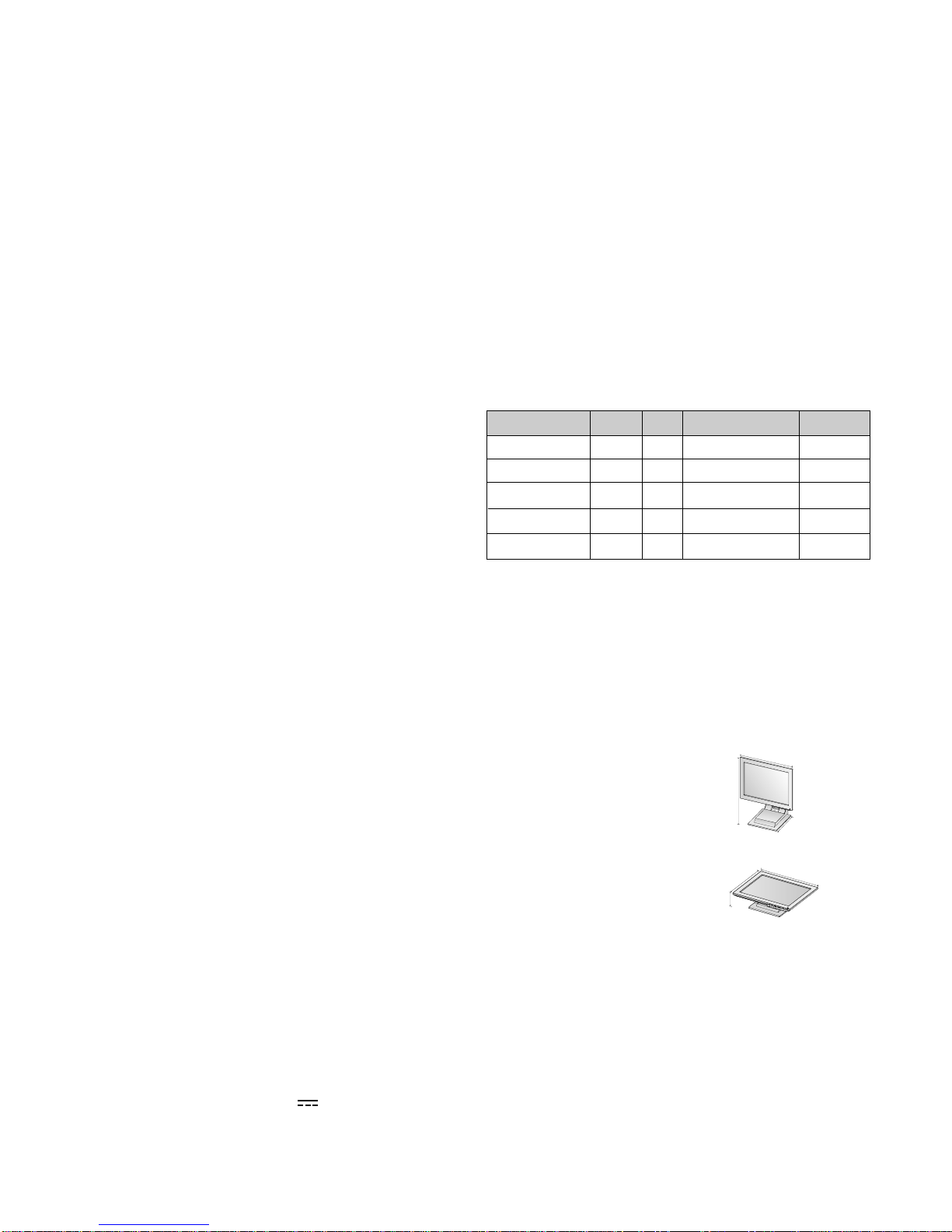
Tilt Range : -37° ~ 145°
You can tilt the screen backward and forward as shown below(Figure A).
Height Range
You can adjust height of the screen(Figure B).
Landscape & Portrait
This monitor offers the ability to rotate between landscape and portrait modes(Figure C).
The monitor rotates from Landscape to Portrait through 90°clockwise and from Portrait to
Landscape through 90°anti-clockwise.
Adjusting the Monitor Position
(Figure A)
-37
+145
(Figure B)
Maximum:
4.87 inch(123.8 mm)
Maximum:
3.863 inch(98.1mm)
(Figure C)
Page 4
- 4 -
To obtain the correct cables and/or to get further instructions on installing them, call the IBM
HELPCENTER at the above numbers or contact your dealer, retailer, or other IBM authorized Servicer.
Alternative mounting options for your IBM Flat Panel Monitor may be available from specialist suppliers.
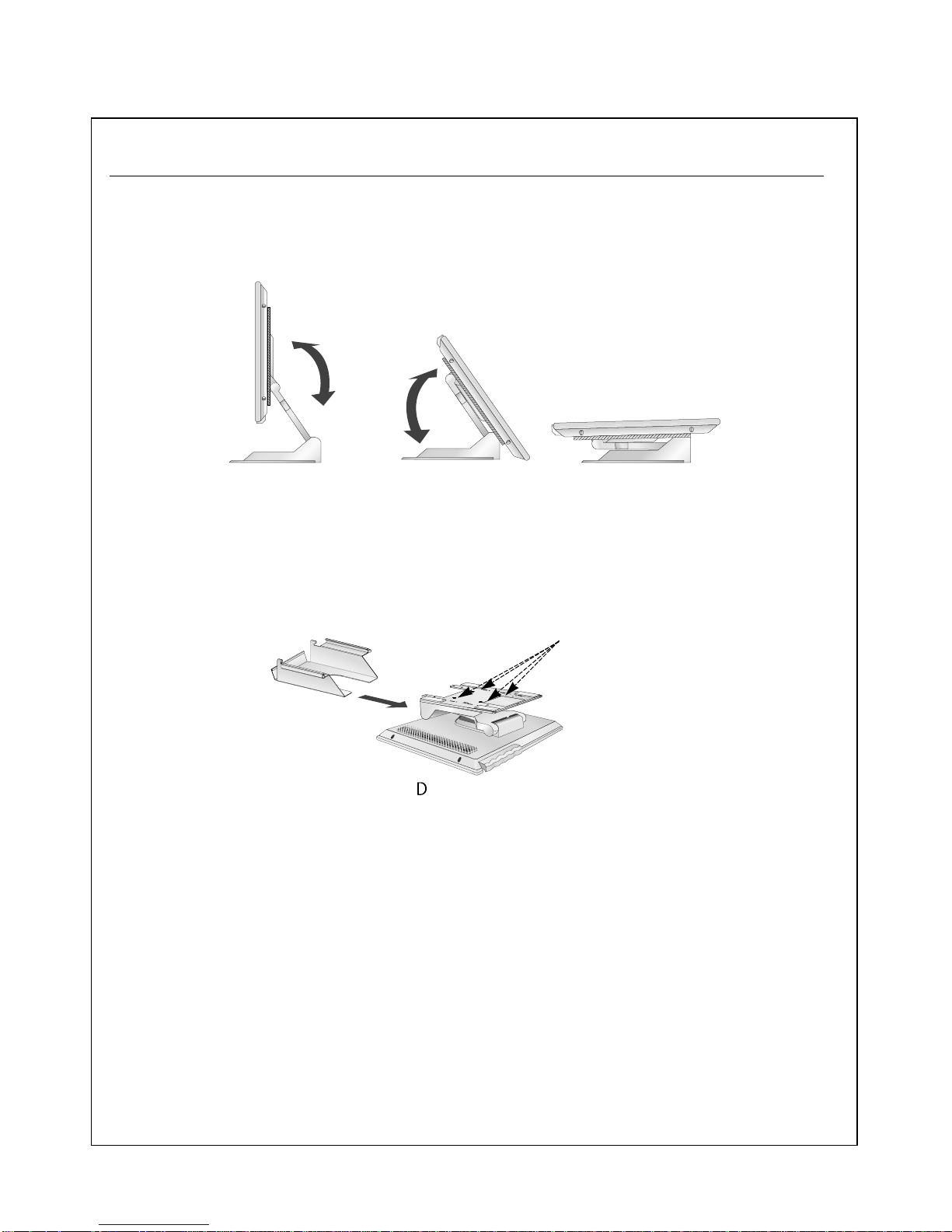
To attach the monitor to an arm or a surface of wall, please follow the instructions below:
1. Power off the monitor.
2. Fold the monitor arm in the order of Figure (A), (B) and (C) as shown above.
3. Place the monitor on a stable and shock-resistant floor, with the front of the monitor at the bottom.
4. Hold the metal clip and push it carefully until it clamps both of the stand and the arm firmly, as shown in
Figure (D) above. (The metal clip is used to keep the arm folded.)
5. You have to use the four screw holds on the bottom of the stand to attach the monitor to the surface of
wall. For additional information, see the instructions supplied with the purchased arm.
6. Locate a place to which you want to attach the monitor. When locating the place, you have to consider
the lengths of the signal cable and the power cord.
7. Attach the monitor to the place you selected in the step 6, and then reconnect the signal cable and the
power cord to the monitor.
(A)
(B)
(C)
( )
Metal clip
Screw holds
VESA Wall Mounting
Page 5

- 5 -
WARNING FOR THE SAFETY-RELATED COMPONENT.
• There are some special components used in LCD
monitor that are important for safety. These parts are
marked on the schematic diagram and the
replacement parts list. It is essential that these critical
parts should be replaced with the manufacturer’s
specified parts to prevent electric shock, fire or other
hazard.
• Do not modify original design without obtaining written
permission from IBM Inc. or you will void the original
parts and labor guarantee.
TAKE CARE DURING HANDLING THE LCD MODULE
WITH BACKLIGHT UNIT.
• Must mount the module using mounting holes arranged
in four corners.
• Do not press on the panel, edge of the frame strongly
or electric shock as this will result in damage to the
screen.
• Do not scratch or press on the panel with any sharp
objects, such as pencil or pen as this may result in
damage to the panel.
• Protect the module from the ESD as it may damage the
electronic circuit (C-MOS).
• Make certain that treatment person’s body are
grounded through wrist band.
• Do not leave the module in high temperature and in
areas of high humidity for a long time.
• The module not be exposed to the direct sunlight.
• Avoid contact with water as it may a short circuit within
the module.
• If the surface of panel become dirty, please wipe it off
with a softmaterial. (Cleaning with a dirty or rough cloth
may damage the panel.)
WARNING
BE CAREFUL ELECTRIC SHOCK !
• If you want to replace with the new backlight (CCFL) or
inverter circuit, must disconnect the AC adapter
because high voltage appears at inverter circuit about
650Vrms.
• Handle with care wires or connectors of the inverter
circuit. If the wires are pressed cause short and may
burn or take fire.
PRECAUTION
CAUTION
Please use only a plastic screwdriver to protect yourself
from shock hazard during service operation.
Page 6

TIMING CHART
- 6 -
H / V
H (Pixels)
V (Lines)
H (Pixels)
V (Lines)
H (Pixels)
V (Lines)
H (Pixels)
V (Lines)
H (Pixels)
V (Lines)
H (Pixels)
V (Lines)
H (Pixels)
V (Lines)
H (Pixels)
V (Lines)
H (Pixels)
V (Lines)
H (Pixels)
V (Lines)
H (Pixels)
V (Lines)
H (Pixels)
V (Lines)
H (Pixels)
V (Lines)
Sync
Polarity
+
–
–
+
–
–
–
–
–
–
+
+
+
+
+
+
+
+
–
–
–
–
–
–
+
+
Dot
Clock
25.175
28.322
25.175
30.24
31.5
36.0
40.0
50.0
49.5
57.2832
65
75
78.75
Frequency
31.468 KHz
70.0 Hz
31.468 KHz
70.0 Hz
31.469 KHz
60.0 Hz
35.00 KHz
66.67 Hz
37.50 KHz
75.0 Hz
35.156 KHz
56.25 Hz
37.879 KHz
60.3 Hz
48.077 KHz
72.188 Hz
46.875 KHz
75.0 Hz
49.725 KHz
74.55 Hz
48.363 KHz
60.0 Hz
56.476 KHz
70.0 Hz
60.023 KHz
75.0 Hz
Resolution
640 x 350
720 x 400
(TEXT)
640 x 480
640 x 480
640 x 480
800 x 600
800 x 600
800 x 600
800 x 600
832 x 624
(MAC)
1024 x 768
1024 x 768
1024 x 768
Total
Period
( E )
800
449
900
449
800
525
864
525
840
500
1024
625
1056
628
1040
666
1056
625
1152
667
1344
806
1328
806
1312
800
Video
Active
Time ( A )
640
350
720
400
640
480
640
480
640
480
800
600
800
600
800
600
800
600
832
624
1024
768
1024
768
1204
768
Blanking
Time
( B )
160
99
180
49
160
45
224
45
200
20
224
25
256
28
240
66
256
25
320
43
320
38
304
38
288
32
Sync
Duration
( D )
96
2
108
2
96
2
64
3
64
3
72
2
128
4
120
6
80
3
64
3
136
6
136
6
96
3
Back
Porch
( F )
48
60
55
34
48
33
96
39
120
16
128
22
88
23
64
23
160
21
224
39
160
29
144
29
176
28
Front
Porch
( C )
16
37
17
13
16
10
64
3
16
1
24
1
40
1
56
37
16
1
32
1
24
3
24
3
16
1
MODE
1
2
3
4
5
6
7
8
9
10
11
12
13
VIDEO
SYNC
C
B
D
F
A
E
Page 7
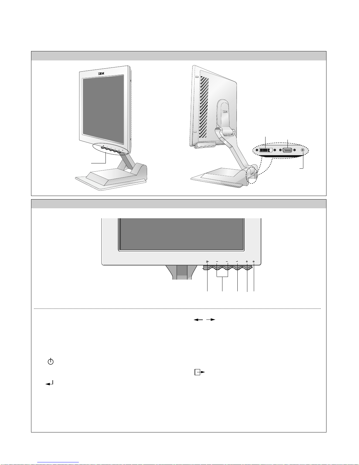
OPERATING INSTRUCTIONS
- 7 -
FRONT VIEW REAR VIEW
Front Control Panel
1. Power Indicator
This indicator lights up green when the monitor
operates normally; In DPMS(Energy Saving) mode,
-stand-by, suspend, or power off mode - its color
changes to orange.
2. Power ON/OFF Button
Switches the monitors on and off.
3. ENTER Button
1) Displays main OSD menu.
2) Enters highlighted menus and submenus.
3) Selects highlighted option.
4. Arrow Key
Moves the cursor to highlight icons or make
adjustments.
1) Brings up Contrast control OSD.
2) Left and Right arrows pressed together bring up
auto setup.
5. Exit Button
1) Exits from menus, sub menus.
2) Exits from OSD.
3
2
1
4
5
Front Control Panel
DVI Port
DSub signal
Adapter Jack
Page 8
WIRING DIAGRAM
- 8 -
P704
P703
J1
Inverter Cable :
6631T11012L
Module link Cable :
6631T11012M
Page 9
Back Cover
- 9 -
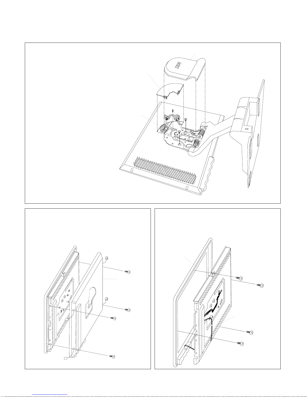
DISASSEMBLY
(a)
(b)
(a)
(c)
1. TILT SWIVEL REMOVAL
(1) Remove the Cover Hinge.
(2) Remove two screws (a).
(3) Remove the Cover Piece Back.
(4) Remove two connectors (c).
(5) Remove the Module Link Cable connector.
(6) Remove the screw (b).
(7) Remove the Tilt Swivel.
2. BACK COVER REMOVAL
(1) Remove four Screw Covers (a).
(2) Remove four screws (b).
(3) Remove the Back Cover Ass’y.
(b)
(b)
(a)
(a)
(a)
(a)
(b)
(b)
3. CABINET ASS’Y REMOVAL
(1) Remove four Screws (a).
(2) Remove the Control PCB connerctor.
(3) Remove the Cabinet Ass’y.
(a)
(a)
(a)
(a)
Cover Hinge
Cover Piece Back
Module Link Cabel
Cabinet
Control PCB Connector
Page 10
- 10 -
(a)
(b)
(c) (c)
(d)
(d)
(d)
(e)
(e)
(d)
(d)
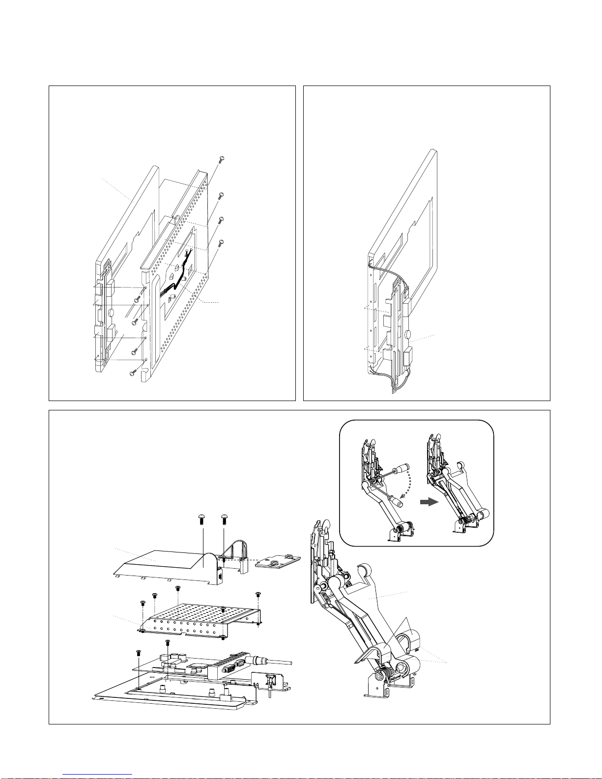
6. TILT SWIVEL ASS’Y REMOVAL
(1) Remove the Cover Hnge (a).
(3) Remove the Cover Stand Body. (Change the Cable)
(2) Remove the Cover Stand Rear(b).
(4) Remove two screws(c).
(5) Remove the Cover Stand Top.
(6) Remove five screws (d) and Metal Shield Main.
(7) Remove two screwS (e).
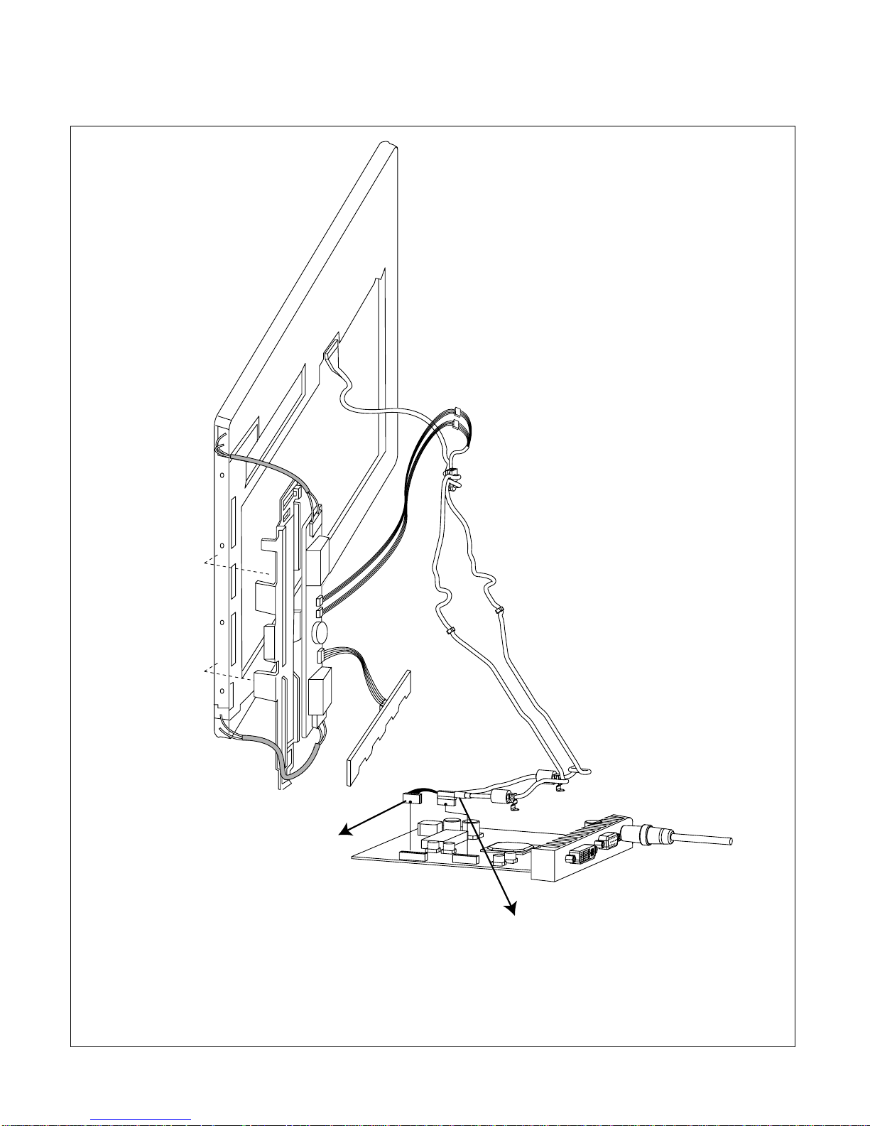
4. LCD MODULE REMOVAL
(1) Remove Inverter Connector.
(2) Remove eight Screws (a).
(3) Remove the Metal Frame from the LCD MODULE.
(a)
(a)
(a)
(a)
(a)
(a)
(a)
(a)
Inverter Connector
5. INVERTER ASS’Y REMOVAL
(1) Disconnector the CN3, CN4.
(2) Remove the Inverter Ass’y.
Inverter Ass’y
Cover Stand Top
Cover Hinge
Remove the Cover Stand Body
Cover Stand Body
Metal Shield Main
LCD Module
Page 11
- 11 -
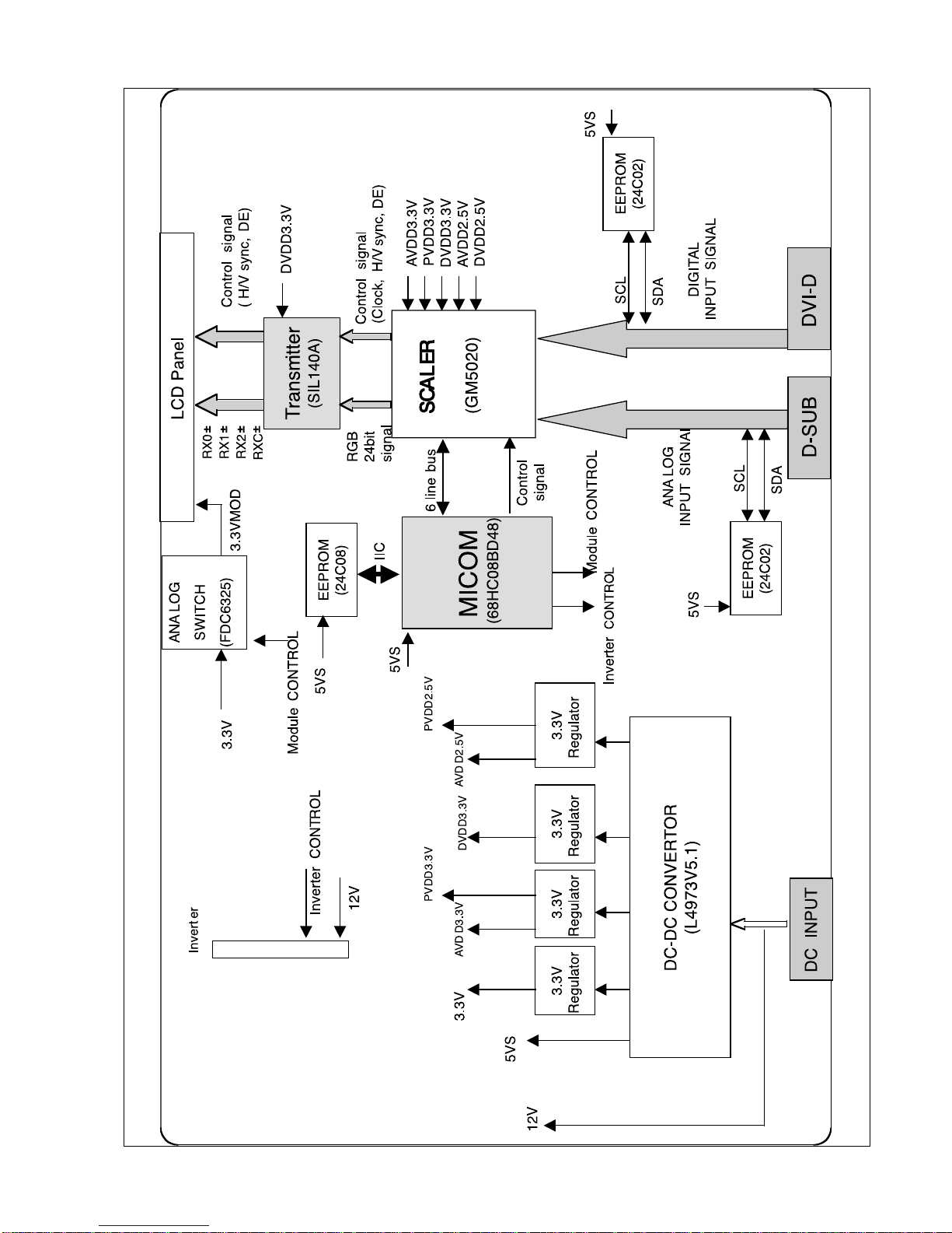
BLOCK DIAGRAM
Page 12

DESCRIPTION OF BLOCK DIAGRAM
- 12 -
1. Genesis Chip (Scaler chip)
GM5020 (U201) is one chip IC which it supports six function block of Video pre amp, PLL, A/D converter
OSD IC, TMDS receiver and scaler.
Video signal (0.7Vp.p) clamped through C204, 210, 211 inputs to U201. These R, G, and B analog signals
converted to 8bit digital signals through pre amp’s amplifying(1/0.7 time) to match AD converter’s operation
range from 0V to 1V and AD converter’s converting analog to 8 bit digital.
Internal PLL inputs horizontal sync signal and outputs clock to ADC and scaler for precise data catching.
Scaler inputs 8bit digital signals and clock, and carries out image processing that interpolates input signal
less than 1024*768 resolution to that of 1024*768 resolution, mixes OSD(On Screen Display) signal by
interfacing with internal OSD IC, and outputs clock, H/V sync, 24bit RGB data, and DE(data enable) signals
which Transmitter(U401) needs.
For supporting digital interface, this IC has internal TMDS receiver converting serial data signal to parallel.
And parallel signal almost similar as 24bit RGB data signal of AD converter’s output goes to scaler which
conducts same operation of analog interface flow that described before.
2. Panel-Link Circuit
Panel link transmitter (U401) delivers digital signal to the receiver inside LCD module by method of abstraction.
The abstracted signals are pairs of TX0+-, TX1+-, TX2+-, TXC+- of which voltage swing is 0.5V each.
Its swing is similar to LVDS (Low Voltage Differential Signal).
Transmitter (U401) gets signals of clock, H/V sync, 24bit RGB data, and DE(data enable) from U201, and outputs
TMDS (Transition Minimized Differential Signal) through TX pins.
When PD pin’s input is low, transmitter goes to power down mode.
3. System Controller (Microprocessor) Circuit
1) Microprocessor (U501) distinguishes polarity and frequency by calculating horizontal and vertical sync input
from signal source.
2) Microprocessor (U501) carries out power control by sending power-down trigger signal to U201, LCD module
and inverter for required power sequence and low power consumption.
3) Microprocessor (U501) communicates with EEPROM (U506), and GM5020 (U201) through IIC(2 lines) or
6 bit bus line. It makes all devices proper operating with communication channel.
4) Microprocessor (U4) lets User adjust screen by each OSD function.
4. DC/ DC Converter
This circuit supplies DC power for each device needing DC voltage of AVDD3.3V, DVDD3.3V, PVDD3.3V,
AVDD2.5V, DVDD2.5V, and 5VST.
L4973D5.1(U803) , the DC/DC controller IC converts input 12Vdc into +5Vdc and +3.3Vdc with peripheral circuit
composed of Coil (L805), condensing components (ZD801, C829, C830) and Regulators (U801, U821).
+3.3VMOD for LCD module power are switched by U802, switching FET, controlled by Microprocessor.
Page 13

ADJUSTMENT
- 13 -
220
IBM
Compatible PC
PARALLEL PORT
Power inlet (required)
Power LED
ST Switch
Power Select Switch
(110V/220V)
Control Line
Not used
RS232C
PARALLEL
V-SYNC
POWER
ST
VGS
MONITOR
E
E
V-Sync On/Off Switch
(Switch must be ON.)
F
F
A
A
B
B
C
C
15
10
5
5
69
1
1
1
14
13
25
6
5V
5V
5V
4.7K
4.7K
4.7K
74LS06
74LS06
OFF ON
OFF
ON
11
Figure 1. Cable Connection
All adjustment are thoroughly checked and corrected
when the monitor leaves the factory, but sometimes
several minor adjustment may be required.
Adjustment should be following procedure and after
warming up for a minimum of 10 minutes.
Alignment appliances and tools.
- IBM Compatible PC
- Programmable Signal Generator.
(eg. VG-819 made by Astrodesign Co.)
- E(E)PROM with each mode data saved.
- Alignment Adapter and Software.
1. Adjustment for Factory Preset Mode
1) Run alignment program for LI561G on the IBM
compatible PC.
2) Select EEPROM all clear command and Enter.
3) Display cross hatch pattern at Mode 1.
4) Select COMMAND PRESET START command.
5) Select FOS DEFAULT command and Enter.
6) Press "Y" key, it will automatically save all FOS data
to EEPROM.
2. Adjustment for White Balance
1) Display color 0,0 pattern at Mode 13.
2) Set External Bright to MAX position and Contrast to
MAX Position.
3) Select PRESET START
→ BIAS CAL command
and Enter.
4) No attempt to manually adjust, BIAS data is automatically adjusted and saved to the EEPROM.
5) Display color 15,0 pattern at Mode 13.
6) Select DRIVE CAL command and Enter.
7) Color 2 (7200K) and Color 3 (9300K) are
automatically adjusted and saved to the EEPROM.
8) Select PRESET EXIT command and Enter.
3. DDC Data Write Procedure
1) Use this procedure only when there is some
probelm on EDID data.
2) Select EEPROM → EDID Write command and
Enter.
3) This will write the EDID data to EEPROM.
Page 14

- 14 -
TROUBLESHOOTING GUIDE
1. NO POWER
CHECK X501.
CHECK
X501’S WAVEFROM
OSCILLATE AS
24MHZ ?
NO
NO POWER
(POWER INDICATOR OFF)
CHECK ADAPTER,
AND FIND OUT
SHORT POINT OF
EACH DC LINE OF
2.5V AND 3.3V
CHECK J801’S
VOLTAGE
(12V) ?
NO
CHECK U803 AND
L805’S OPEN
CHECK
U803 PIN 2, 3
WAVEFROM?
NO
YES
YES
YES
CHECK KEY CONTROL
CONNECTOR ROUTINE
200kHz
40% duty
12V
Page 15

- 15 -
2. NO RASTER (OSD IS NOT DISPLAYED) – INVERTER
CHECK MICOM INV
ON/OFF PORT.
J703 PIN5
5V?
NO
NO RASTER
(OSD IS NOT DISPLAYED)
CHECK ADAPTER
J703 PIN10
12V?
NO
1. CONFIRM BRIGHTNESS
OSD CONTRL STATE.
2. CHECK MICOM DIM-ADJ
PORT
J703 PIN1
5V?
NO
REPLACE
INVERTER ASS’Y
CHECK
PULSE AS
CONTACTING SCOPE
PROBE TO CAUTION LABEL.
(CONTACT PROBE TO
CAUTION LABEL.
CAN YOU SEE PULSE
AT YOUR
SCOPE?
NO
REPLACE CCFL LAMP
IN THE LCD MODULE
YES
YES
YES
YES
Page 16

CHECK U802, U881
NO
- 16 -
1. CHECK PIN34, 35
SOLDERING CONDITION
2. CHECK X201
3. TROUBLE IN U201
U821
POWER PINS
3.3V, 2.5V?
NO
CHECK U801, U821
X201
OSCILLATE AS 24M?
NO
CHECK U201 OR U401’S
SOLDERING CONDITION
AND CHECK CONNECTION
LINE FROM U201 TO U401
NO
TROUBLE IN CABLE
OR LCD MODULE
J703’S PIN1
3.3V?
YES
YES
YES
YES
3. WHITE SCREEN (OSD IS NOT DISPLAYED)
WHITE SCREEN
(OSD IS NOT DISPLAYED)
U401
PIN12 IS 65MHz CLOCK?
PIN2 IS 48KHz H-SYNC?
PIN3 IS 60Hz V-SYNC?
PIN1 IS 48KHz H-SYNC?
IS PULSE APPEARED
AT SIGNAL
PINS?
Input
1024x768@60Hz Signal.
Page 17

- 17 -
CHECK
CMF 401, 402,
403, 404’S
WAVEFORM?
NO
CHECK U401
CHECK J703’S
SOLDERING CONDITION
YES
4. RAINBOW SCREEN
RAINBOW SCREEN
(OSD IS NOT DISPLAYED)
Page 18

PRINTED CIRCUIT BOARD
- 18 -
1. MAIN BOARD (Component Side)
C825
C824
C827
R805
R804
U821
C828
C802
C803
C801
R801
R806
U803
15
20
C826
R5
C806
R210
C534
L803
L801
L703
L702
L701
J801
C832
1
10
U801
R7
R6
C808
C807
L802
C809
C535
R1
R541
R539
R542
R540
C530
R537
L503
L1
C831
ZD801
C510
R506
C512
C515
C511
R504
R505
R503
C513
C538
R507
R502
C841
C840
R8
X201
C201
R216
C202
U504
C533
C528
R535
Q501
D713
D717
J702
U506
C539
R229
R208
Y
W
V
U
T
R
R215
R201
J
KLMPN
R217
C
D
EFG
H
L502
U201
1
A
B
R538
Q502
R523
R509
234 567
L805
R545
C540
C541
R543
R508
R544
8 9 10 11 12 13
U503
D720 D714
R555
R556
R557
R558
R563
R562
R561
R560
C829
C502
R510
C537
U510
14 15 16 17 18 19
ZD703
D710 D712
D701
C834
C833
C543
C542
R809
R554
R559
R567
R525
C501 R501
X501
BA204 BA205
20
C280
R548
R547
C219
R549
R546
R228
D716
C830
C821
BA201
C234
L203
L202
BA202
BA203
BA206
C268 C267 C266
C210
C211
C204
C282
C281
C213
C215
R220
R221
R222
R223
R226
R224
R225
R227
D708 D709
ZD705
C429
C425
C433
R409
R408
L810
U501
L204
CA201
C217
C233
1
CA202
60
CA204
CA203
50
CA206
CA205
ZD702
C414
C702
C701
R721
R720
ZD701
D705
D706 D707
L707
C422 C423 C424
C427
C428
L706
C431
C432
R406
R407
C820
L804
10
U401
40
C401
R402
L401
C415
D704D703
P/N :6870T326A12
DATE :2001.07.16
MODEL:LI561G(IBM)
R740
R743
C426
R536
R534
R533
Q705
C430
R529
L403
20
CMF403
30
CMF404
R401
C819
R803
J701
R739
R742
C712
R710
Q704
L705
L712
L711
L710
C719
C718
C713
CMF401
CMF402
C417
C416
R711
R736
R737
C818
C837
L402
U881
U802
R802
C709
C710
R735
R734
D504
ZD704
D505
C711
R741
J704
1
L720
L714
L713
L715
C421
J703
C817
C816
R738
ZD502
R551
R553
R552
ZD501
C536
R550
U505
Page 19

- 19 -
2. MAIN BOARD (Solder Side)
C810
C813
R808
R807
C835
C836
C812
C815
C811
C814
C265
C277
C272
C269
C278
C284
R519
C216
C218
C225
C226
C804
C256
C255
C257
C285
C286
R219
R520
R521
R522
R207
C229
C249
C261
C260
C289
C288
C287
R724
R723
R722
R725
R726
R518
C505
C205
C206
C207
C250
C262
R218
C290
C291
C292
R728
R727
R511
R512
C212
C208
C209
C263
C264
C294
C295
C293
R516
R532
C507
C508
C214
C238
C203
C274
C296
R701
C506
R517
C509
R531
L201
C275
C276
R702
R704
R703
R709
C504
C842
C843
C404
C419
C408
C418
C420C240
C241
C239
C237
C245
C251
R706
R705
C503
C402
R9
C405
R403
R405
C409
C242
C243
C244
C412
C411
C248
C247
C246
C253
C254
C252
R708
R707
C403
C410
C406
C413
C838
C850
R810
C714
C407
C839
C715
25
20
30
15
35
10
5
40
1
Page 20

- 20 -
1
2
7
6
5
8
9
3
10
14
15
16
17
20
30
29
21
23
24
22
25
27
28
26
19
12
11
4
13
32
31
18
EXPLODED VIEW
Page 21

- 21 -
EXPLODED VIEW PARTS LIST
Ref. No.
1
2
3
4
5
6
7
8
9
10
11
12
13
14
15
16
17
18
19
20
21
22
23
Part No.
3091TKL026B
3091TKL026A
6304FLP002A
3809TKL018B
3809TKL018A
3043TKK075B
3043TKK075A
3680TKP060A
4940TKT135B
4940TKT135A
6871TST252A
4810TKK161A
6633TZA003J
4950TKS170A
4950TKS170B
6631T12001U
3550TKK201B
3550TKK201A
3550TKK194B
3550TKK194A
4951TKK070B
4951TKK070A
4951TKK058B
4951TKK058A
4810TKK172B
4810TKK172A
4951TKK059B
4951TKK059A
6631T11012M
6631T11012L
3550TKK200B
3550TKK200A
4814TKK180A
4951TKK061C
DESCRIPTION
CABINET ASSEMBLY, LI561G IBM 3090TKL024A (PEARL WHITE)
CABINET ASSEMBLY, LI561G IBM 3090TKL024A (STEALTH BLACK)
LCD(LIQUID CRYSTAL DISPLAY), LM150X04-A3 LG PHILPS TFT COLOR 15.0" 6 BIT+FRC XG
BACK COVER ASSEMBLY, LI561G 3808TKL020A (PEARL WHITE)
BACK COVER ASSEMBLY, LI561G 3808TKL020A (STEALTH BLACK)
TILT SWIVEL ASSY, LI561G . IBM(T565) (PEARL WHITE)
TILT SWIVEL ASSY, LI561G . IBM(T565) (STEALTH BLACK)
LENS, POWER LED LI561G
KNOB, TACT CONTROL LI561G (LIGHT SAGE GRAY)
KNOB, TACT CONTROL LI561G (RAVEN BLACK)
PWB(PCB) ASSEMBLY,SUB, LI561G CONTROL TOTAL IBM T565
BRACKET, LI561G HOLDER INVERTER
INVERTER ASSEMBLY SAMSUNG LG1506 ,2 LAMP,LI561G
METAL FRAME SBHG(T=0.8),LI561G
METAL FRAME LI561G(METAL-SPRAY) (RAVEN BLACK)
CONNECTOR ASSEMBLY, 12P H-H 300MM UL 1061#28
COVER LI561G PIECE BACK (PEARL WHITE)
COVER LI561G PIECE BACK (STEALTH BLACK)
COVER LI561G HINGE ROTATE (PEARL WHITE)
COVER LI561G HINGE ROTATE (STEALTH BLACK)
METAL ASSEMBLY, PLATE CLIP (PEARL WHITE)
METAL ASSEMBLY, PLATE CLIP (STEALTH BLACK)
METAL ASSY, TILT UNIT ROTATE(PEARL WHITE).LI561G (PEARL WHITE)
METAL ASSY, TILT UNIT ROTATE(BK). LI561G (STEALTH BLACK)
BRACKET, LI561G GUIDE HINGE ROTATE (PEARL WHITE)
BRACKET HINGE GUIDE ROTATE (STEALTH BLACK)
METAL ASSY, TILT UNIT TOP LEFT LI561G
METAL ASSY, TILT UNIT TOP RIGHT LI561G
CONNECTOR ASSEMBLY, 21P H-H 587MM UL 2725 #32 PANELINK CABLE LI561G
CONNECTOR ASSEMBLY, 12P H-H 701MM UL 2725 #30 INVERTER CABLE LI561G
COVER LI561G STAND BODY (PEARL WHITE)
COVER LI561G STAND BODY (STEALTH BLACK)
SHIELD SIDE CABLE LI561G
METAL ASSY, TILT UNIT BOTTOM ONE SHAFT LI561G
Page 22

- 22 -
EXPLODED VIEW PARTS LIST
Ref. No.
24
25
26
27
28
29
30
31
32
Part No.
4950TKK322B
4950TKK322A
3550TKK196B
3550TKK196A
3550TKK197B
3550TKK197A
4930TKK035A
3550TKK199B
3550TKK199A
3313TL5032A
4950TKK321A
3550TKK198B
3550TKK198A
3550TKK195B
3550TKK195A
DESCRIPTION
METAL SUPPORT AL DIE-CASTING (PEARL WHITE)
METAL SUPPORT AL D CASTING LI561G (STEALTH BLACK)
COVER LI561G HINGE LEFT (PEARL WHITE)
COVER LI561G HINGE LEFT (STEALTH BLACK)
COVER, LI561G HINGE RIGHT (PEARL WHITE)
COVER, LI561G HINGE RIGHT (STEALTH BLACK)
HOLDER, CABLE DAMB-05
COVER LI561G STAND BOTTOM (LIGHT SAGE GRAY)
COVER LI561G STAND BOTTOM (RAVEN BLACK)
MAIN TOTAL ASSEMBLY, LI561G IBM CL-25
METAL SHIELD MAIN LI561G
COVER LI561G STAND TOP (PEARL WHITE)
COVER LI561G STAND TOP (STEALTH BLACK)
COVER LI561G STAND REAR (PEARL WHITE)
COVER LI561G STAND REAR (STEALTH BLACK)
Page 23

- 23 -
MODEL: T560(6656-HW2)/ T560(6656-HG2) DATE: 2001. 8. 17.
*S *AL LOC. NO. PART NO. DESCRIPTION / SPECIFICATION
C201 0CC100CK41A 10PF 1608 50V 5% R/TP NP0
C202 0CC100CK41A 10PF 1608 50V 5% R/TP NP0
C203 0CC330CK41A 33PF 1608 50V 5% R/TP NP0
C204 0CK103CK51A 0.01UF 1608 50V 10% R/TP B(Y5P
C205 0CC221CK41A 220PF 1608 50V 5% R/TP NP0
C206 0CC221CK41A 220PF 1608 50V 5% R/TP NP0
C207 0CC221CK41A 220PF 1608 50V 5% R/TP NP0
C208 0CC221CK41A 220PF 1608 50V 5% R/TP NP0
C209 0CC221CK41A 220PF 1608 50V 5% R/TP NP0
C210 0CK103CK51A 0.01UF 1608 50V 10% R/TP B(Y5P
C211 0CK103CK51A 0.01UF 1608 50V 10% R/TP B(Y5P
C212 0CC221CK41A 220PF 1608 50V 5% R/TP NP0
C213 0CC100CK41A 10PF 1608 50V 5% R/TP NP0
C214 0CC221CK41A 220PF 1608 50V 5% R/TP NP0
C215 0CC100CK41A 10PF 1608 50V 5% R/TP NP0
C216 0CC221CK41A 220PF 1608 50V 5% R/TP NP0
C217 0CC330CK41A 33PF 1608 50V 5% R/TP NP0
C218 0CC221CK41A 220PF 1608 50V 5% R/TP NP0
C219 0CC100CK41A 10PF 1608 50V 5% R/TP NP0
C225 0CK104CK56A 0.1UF 1608 50V 10% R/TP X7R
C226 0CC221CK41A 220PF 1608 50V 5% R/TP NP0
C229 0CC221CK41A 220PF 1608 50V 5% R/TP NP0
C233 0CC680CK41A 68PF 1608 50V 5% R/TP NP0
C234 0CC680CK41A 68PF 1608 50V 5% R/TP NP0
C237 0CK104CK56A 0.1UF 1608 50V 10% R/TP X7R
C238 0CC101CK41A 100PF 1608 50V 5% R/TP NP0
C239 0CK104CK56A 0.1UF 1608 50V 10% R/TP X7R
C240 0CK104CK56A 0.1UF 1608 50V 10% R/TP X7R
C241 0CK104CK56A 0.1UF 1608 50V 10% R/TP X7R
C242 0CK104CK56A 0.1UF 1608 50V 10% R/TP X7R
C243 0CK104CK56A 0.1UF 1608 50V 10% R/TP X7R
C244 0CK104CK56A 0.1UF 1608 50V 10% R/TP X7R
C245 0CK104CK56A 0.1UF 1608 50V 10% R/TP X7R
C246 0CK104CK56A 0.1UF 1608 50V 10% R/TP X7R
C247 0CK104CK56A 0.1UF 1608 50V 10% R/TP X7R
C248 0CK104CK56A 0.1UF 1608 50V 10% R/TP X7R
C249 0CK104CK56A 0.1UF 1608 50V 10% R/TP X7R
C250 0CC221CK41A 220PF 1608 50V 5% R/TP NP0
C251 0CK104CK56A 0.1UF 1608 50V 10% R/TP X7R
C252 0CK104CK56A 0.1UF 1608 50V 10% R/TP X7R
C253 0CK104CK56A 0.1UF 1608 50V 10% R/TP X7R
C254 0CK104CK56A 0.1UF 1608 50V 10% R/TP X7R
C255 0CC221CK41A 220PF 1608 50V 5% R/TP NP0
C256 0CK104CK56A 0.1UF 1608 50V 10% R/TP X7R
C257 0CC221CK41A 220PF 1608 50V 5% R/TP NP0
C260 0CK104CK56A 0.1UF 1608 50V 10% R/TP X7R
C261 0CK104CK56A 0.1UF 1608 50V 10% R/TP X7R
C262 0CC221CK41A 220PF 1608 50V 5% R/TP NP0
C263 0CK104CK56A 0.1UF 1608 50V 10% R/TP X7R
C264 0CK104CK56A 0.1UF 1608 50V 10% R/TP X7R
C265 0CK104CK56A 0.1UF 1608 50V 10% R/TP X7R
C266 0CC150CK41A 15PF 1608 50V 5% R/TP NP0
C267 0CC150CK41A 15PF 1608 50V 5% R/TP NP0
C268 0CC150CK41A 15PF 1608 50V 5% R/TP NP0
C269 0CC221CK41A 220PF 1608 50V 5% R/TP NP0
MODEL: T560(6656-HW2)/ T560(6656-HG2) DATE: 2001. 8. 17.
*S *AL LOC. NO. PART NO. DESCRIPTION / SPECIFICATION
C272 0CC221CK41A 220PF 1608 50V 5% R/TP NP0
C274 0CK104CK56A 0.1UF 1608 50V 10% R/TP X7R
C275 0CC221CK41A 220PF 1608 50V 5% R/TP NP0
C276 0CC221CK41A 220PF 1608 50V 5% R/TP NP0
C277 0CC221CK41A 220PF 1608 50V 5% R/TP NP0
C278 0CC221CK41A 220PF 1608 50V 5% R/TP NP0
C280 0CK103CK51A 0.01UF 1608 50V 10% R/TP B(Y5P
C281 0CK103CK51A 0.01UF 1608 50V 10% R/TP B(Y5P
C282 0CK103CK51A 0.01UF 1608 50V 10% R/TP B(Y5P
C284 0CK104CK56A 0.1UF 1608 50V 10% R/TP X7R
C285 0CK104CK56A 0.1UF 1608 50V 10% R/TP X7R
C286 0CC221CK41A 220PF 1608 50V 5% R/TP NP0
C287 0CK104CK56A 0.1UF 1608 50V 10% R/TP X7R
C288 0CK104CK56A 0.1UF 1608 50V 10% R/TP X7R
C289 0CK104CK56A 0.1UF 1608 50V 10% R/TP X7R
C290 0CK104CK56A 0.1UF 1608 50V 10% R/TP X7R
C291 0CK104CK56A 0.1UF 1608 50V 10% R/TP X7R
C292 0CK104CK56A 0.1UF 1608 50V 10% R/TP X7R
C293 0CC221CK41A 220PF 1608 50V 5% R/TP NP0
C294 0CC221CK41A 220PF 1608 50V 5% R/TP NP0
C295 0CC221CK41A 220PF 1608 50V 5% R/TP NP0
C296 0CC221CK41A 220PF 1608 50V 5% R/TP NP0
C401 0CC680CK41A 68PF 1608 50V 5% R/TP NP0
C402 0CK104CK56A 0.1UF 1608 50V 10% R/TP X7R
C403 0CH3105F946 1UF 16V Z F 2012 R/TP
C404 0CC680CK41A 68PF 1608 50V 5% R/TP NP0
C405 0CK104CK56A 0.1UF 1608 50V 10% R/TP X7R
C408 0CK104CK56A 0.1UF 1608 50V 10% R/TP X7R
C409 0CK104CK56A 0.1UF 1608 50V 10% R/TP X7R
C410 0CK104CK56A 0.1UF 1608 50V 10% R/TP X7R
C411 0CK104CK56A 0.1UF 1608 50V 10% R/TP X7R
C412 0CK104CK56A 0.1UF 1608 50V 10% R/TP X7R
C413 0CK104CK56A 0.1UF 1608 50V 10% R/TP X7R
C414 0CH8107F611 100UF 16V M 85STD(CYL) R/TP
C415 0CH8107F611 100UF 16V M 85STD(CYL) R/TP
C416 0CK104CK56A 0.1UF 1608 50V 10% R/TP X7R
C417 0CH3105F946 1UF 16V Z F 2012 R/TP
C418 0CC680CK41A 68PF 1608 50V 5% R/TP NP0
C419 0CH3105F946 1UF 16V Z F 2012 R/TP
C420 0CK104CK56A 0.1UF 1608 50V 10% R/TP X7R
C421 0CH8107F611 100UF 16V M 85STD(CYL) R/TP
C422 0CH3105F946 1UF 16V Z F 2012 R/TP
C423 0CH3105F946 1UF 16V Z F 2012 R/TP
C424 0CH3105F946 1UF 16V Z F 2012 R/TP
C425 0CK104CK56A 0.1UF 1608 50V 10% R/TP X7R
C426 0CK104CK56A 0.1UF 1608 50V 10% R/TP X7R
C427 0CK104CK56A 0.1UF 1608 50V 10% R/TP X7R
C428 0CK104CK56A 0.1UF 1608 50V 10% R/TP X7R
C429 0CH3105F946 1UF 16V Z F 2012 R/TP
C430 0CK104CK56A 0.1UF 1608 50V 10% R/TP X7R
C431 0CK104CK56A 0.1UF 1608 50V 10% R/TP X7R
C432 0CK104CK56A 0.1UF 1608 50V 10% R/TP X7R
C433 0CK104CK56A 0.1UF 1608 50V 10% R/TP X7R
C501 0CC120CK41A 12PF 1608 50V 5% R/TP NP0
C502 0CC120CK41A 12PF 1608 50V 5% R/TP NP0
C503 0CC102CK41A 1000PF 1608 50V 5% R/TP NP0
C504 0CK104CK56A 0.1UF 1608 50V 10% R/TP X7R
REPLACEMENT PARTS LIST
CAUTION: BEFORE REPLACING ANY OF THESE COMPONENTS,
READ CAREFULLY THE SAFETY PRECAUTIONS IN THIS MANUAL.
* NOTE : S SAFETY Mark
AL ALTERNATIVE PARTS
MAIN BOARD
CAPACITORS
Page 24

MODEL: T560(6656-HW2)/ T560(6656-HG2) DATE: 2001. 8. 17.
*S *AL LOC. NO. PART NO. DESCRIPTION / SPECIFICATION
C505 0CC101CK41A 100PF 1608 50V 5% R/TP NP0
C506 0CK222CK51A 2200PF 1608 50V 10% R/TP B(Y5P
C507 0CK104CK56A 0.1UF 1608 50V 10% R/TP X7R
C508 0CK104CK56A 0.1UF 1608 50V 10% R/TP X7R
C509 0CK104CK56A 0.1UF 1608 50V 10% R/TP X7R
C510 0CC470CK41A 47PF 1608 50V 5% R/TP NP0
C511 0CC470CK41A 47PF 1608 50V 5% R/TP NP0
C512 0CC470CK41A 47PF 1608 50V 5% R/TP NP0
C513 0CC470CK41A 47PF 1608 50V 5% R/TP NP0
C515 0CC470CK41A 47PF 1608 50V 5% R/TP NP0
C528 0CC680CK41A 68PF 1608 50V 5% R/TP NP0
C530 0CC680CK41A 68PF 1608 50V 5% R/TP NP0
C533 0CK104CK56A 0.1UF 1608 50V 10% R/TP X7R
C534 0CC101CK41A 100PF 1608 50V 5% R/TP NP0
C535 0CC101CK41A 100PF 1608 50V 5% R/TP NP0
C536 0CK104CK56A 0.1UF 1608 50V 10% R/TP X7R
C537 0CK104CK56A 0.1UF 1608 50V 10% R/TP X7R
C538 0CC470CK41A 47PF 1608 50V 5% R/TP NP0
C539 0CK104CK56A 0.1UF 1608 50V 10% R/TP X7R
C540 0CC101CK41A 100PF 1608 50V 5% R/TP NP0
C541 0CC101CK41A 100PF 1608 50V 5% R/TP NP0
C542 0CC101CK41A 100PF 1608 50V 5% R/TP NP0
C543 0CC101CK41A 100PF 1608 50V 5% R/TP NP0
C701 0CC101CK41A 100PF 1608 50V 5% R/TP NP0
C702 0CC101CK41A 100PF 1608 50V 5% R/TP NP0
C709 0CC101CK41A 100PF 1608 50V 5% R/TP NP0
C710 0CC101CK41A 100PF 1608 50V 5% R/TP NP0
C711 0CK104CK56A 0.1UF 1608 50V 10% R/TP X7R
C712 0CK104CK56A 0.1UF 1608 50V 10% R/TP X7R
C713 0CH8107J611 100UF 35V M 85STD(CYL) R/TP
C714 0CC221CK41A 220PF 1608 50V 5% R/TP NP0
C715 0CC221CK41A 220PF 1608 50V 5% R/TP NP0
C718 0CK103CK51A 0.01UF 1608 50V 10% R/TP B(Y5P
C719 0CK103CK51A 0.01UF 1608 50V 10% R/TP B(Y5P
C801 0CK104CK56A 0.1UF 1608 50V 10% R/TP X7R
C802 0CH8477F691 470UF 16V M 105STD (CYL) R/TP
C803 0CK104CK56A 0.1UF 1608 50V 10% R/TP X7R
C804 0CK104CK56A 0.1UF 1608 50V 10% R/TP X7R
C806 0CH8107F611 100UF 16V M 85STD(CYL) R/TP
C807 0CZZTAT002B SVP SANYO 10V 47UF M REEL OS-C
C808 0CH8107F611 100UF 16V M 85STD(CYL) R/TP
C809 0CH8107F611 100UF 16V M 85STD(CYL) R/TP
C810 0CK104CK56A 0.1UF 1608 50V 10% R/TP X7R
C811 0CC102CK41A 1000PF 1608 50V 5% R/TP NP0
C812 0CK104CK56A 0.1UF 1608 50V 10% R/TP X7R
C813 0CK104CK56A 0.1UF 1608 50V 10% R/TP X7R
C814 0CC102CK41A 1000PF 1608 50V 5% R/TP NP0
C815 0CC102CK41A 1000PF 1608 50V 5% R/TP NP0
C816 0CK104CK56A 0.1UF 1608 50V 10% R/TP X7R
C817 0CC102CK41A 1000PF 1608 50V 5% R/TP NP0
C818 0CH8107F611 100UF 16V M 85STD(CYL) R/TP
C819 0CC102CK41A 1000PF 1608 50V 5% R/TP NP0
C820 0CH8107F611 100UF 16V M 85STD(CYL) R/TP
C821 0CH8107F611 100UF 16V M 85STD(CYL) R/TP
C824 0CH3105F946 1UF 16V Z F 2012 R/TP
C825 0CH3105F946 1UF 16V Z F 2012 R/TP
C826 0CC221CK41A 220PF 1608 50V 5% R/TP NP0
C827 0CK223CK51A 0.022UF 1608 50V 10% R/TP B(Y5
C828 0CH8107J611 100UF 35V M 85STD(CYL) R/TP
C829 0CH8477F691 470UF 16V M 105STD (CYL) R/TP
C830 0CH8477F691 470UF 16V M 105STD (CYL) R/TP
C831 0CC102CK41A 1000PF 1608 50V 5% R/TP NP0
C832 0CK152CK51A 1500PF 1608 50V 10% R/TP B(Y5P
C833 0CK104CK56A 0.1UF 1608 50V 10% R/TP X7R
C834 0CK103CK51A 0.01UF 1608 50V 10% R/TP B(Y5P
C835 0CK104CK56A 0.1UF 1608 50V 10% R/TP X7R
MODEL: T560(6656-HW2)/ T560(6656-HG2) DATE: 2001. 8. 17.
*S *AL LOC. NO. PART NO. DESCRIPTION / SPECIFICATION
C836 0CK104CK56A 0.1UF 1608 50V 10% R/TP X7R
C837 0CH8107F611 100UF 16V M 85STD(CYL) R/TP
C838 0CC102CK41A 1000PF 1608 50V 5% R/TP NP0
C839 0CK104CK56A 0.1UF 1608 50V 10% R/TP X7R
C840 0CK104CK56A 0.1UF 1608 50V 10% R/TP X7R
C841 0CC102CK41A 1000PF 1608 50V 5% R/TP NP0
C842 0CC102CK41A 1000PF 1608 50V 5% R/TP NP0
C843 0CK104CK56A 0.1UF 1608 50V 10% R/TP X7R
C850 0CK104CK56A 0.1UF 1608 50V 10% R/TP X7R
D504 0DS301109AA MMBD301LT1 TP MOTOROLA SOT23 3
D505 0DS301109AA MMBD301LT1 TP MOTOROLA SOT23 3
D701 0DS226009AA KDS226 TP KEC SOT-23 80V 300M
D703 0DS226009AA KDS226 TP KEC SOT-23 80V 300M
D704 0DS226009AA KDS226 TP KEC SOT-23 80V 300M
D705 0DS226009AA KDS226 TP KEC SOT-23 80V 300M
D706 0DS226009AA KDS226 TP KEC SOT-23 80V 300M
D707 0DS226009AA KDS226 TP KEC SOT-23 80V 300M
D708 0DS226009AA KDS226 TP KEC SOT-23 80V 300M
D709 0DS226009AA KDS226 TP KEC SOT-23 80V 300M
D710 0DS226009AA KDS226 TP KEC SOT-23 80V 300M
D712 0DS226009AA KDS226 TP KEC SOT-23 80V 300M
D713 0DS226009AA KDS226 TP KEC SOT-23 80V 300M
D714 0DS226009AA KDS226 TP KEC SOT-23 80V 300M
D716 0DS226009AA KDS226 TP KEC SOT-23 80V 300M
D717 0DS226009AA KDS226 TP KEC SOT-23 80V 300M
D720 0DS226009AA KDS226 TP KEC SOT-23 80V 300M
ZD501 0DZ560009DA UDZ S 5.6B TP ROHM-K SOD323 20
ZD502 0DZ560009DA UDZ S 5.6B TP ROHM-K SOD323 20
ZD701 0DZ560009DA UDZ S 5.6B TP ROHM-K SOD323 20
ZD702 0DZ560009DA UDZ S 5.6B TP ROHM-K SOD323 20
ZD703 0DZ560009DA UDZ S 5.6B TP ROHM-K SOD323 20
ZD704 0DZ560009DA UDZ S 5.6B TP ROHM-K SOD323 20
ZD705 0DZ560009DA UDZ S 5.6B TP ROHM-K SOD323 20
ZD801 0DR340009AA MBRS340 TP FAIRCHILD NON 40V 3
U201 0IPRPGN001A GM5020 GENESIS 292P,PBGA TRAY
U401 0IPRPS5001A SII140A SILICON IMAGE 64P,TQFP
U501 0IZZTSZ148A DIP 42P BK OTP LI561G
U503 0ICS240213A CAT24WC02J-TE13 8P SOP TP 2K I
U504 0IMO741420B MC74HCT14ADR2 14P,SOIC TP LEVE
U505 0ICS240213A CAT24WC02J-TE13 8P SOP TP 2K I
U506 0ICS240813B CAT24WC08J-TE13 8P,SOIC R/TP 8
U510 0IKE704200J KIA7042AF SOT-89 TP 4.2V VOLTA
U801 0IPMGFA007A RC1616S25T FAIRCHILD SOT223 R/
U802 0TF632509AA FDC6325L TP FAIRCHILD 8V 2.4A
U803 0ISG497351A L4973D5.1 SO20 TP 3.5A S/DOWN
U821 0IRH033200A BA033FP-E2 MOLD-3 TP REGULATOR
U881 0IRH033200A BA033FP-E2 MOLD-3 TP REGULATOR
L1 6210TCE001G HH-1M3216-501 CERATEC 3216MM R
L201 6210TCE001P HB-1S2012-121JT CERATECH 2012M
L202 6210TCE001K HB-1H2012-260JT CERATEC 2012MM
L203 6210TCE001P HB-1S2012-121JT CERATECH 2012M
L204 6210TCE001P HB-1S2012-121JT CERATECH 2012M
L401 6210TCE001U HB-1M3216-102JT CERATECH 3216M
L402 6210TCE001U HB-1M3216-102JT CERATECH 3216M
L403 6210TCE001U HB-1M3216-102JT CERATECH 3216M
L502 6210TCE001P HB-1S2012-121JT CERATECH 2012M
L503 6210TCE001P HB-1S2012-121JT CERATECH 2012M
- 24 -
DIODEs
ICs
COILs & COREs
Page 25

MODEL: T560(6656-HW2)/ T560(6656-HG2) DATE: 2001. 8. 17.
*S *AL LOC. NO. PART NO. DESCRIPTION / SPECIFICATION
L701 6210TCE001K HB-1H2012-260JT CERATEC 2012MM
L702 6210TCE001K HB-1H2012-260JT CERATEC 2012MM
L703 6210TCE001K HB-1H2012-260JT CERATEC 2012MM
L705 6210TCE001D HB-1M2012-601JT CERATEC 2012MM
L707 6210TCE001G HH-1M3216-501 CERATEC 3216MM R
L710 6210TCE001D HB-1M2012-601JT CERATEC 2012MM
L711 6210TCE001D HB-1M2012-601JT CERATEC 2012MM
L712 6210TCE001D HB-1M2012-601JT CERATEC 2012MM
L713 6210TCE001D HB-1M2012-601JT CERATEC 2012MM
L714 6210TCE001D HB-1M2012-601JT CERATEC 2012MM
L715 0RH0000D622 0 1/10W P-TYPE TAPPING
L720 6210TCE001D HB-1M2012-601JT CERATEC 2012MM
L802 6210TCE001G HH-1M3216-501 CERATEC 3216MM R
L803 6210TCE001G HH-1M3216-501 CERATEC 3216MM R
L804 6210TCE001G HH-1M3216-501 CERATEC 3216MM R
L805 6200TEZ003D TPRH1207-330M BOAM R/TP 33 UH
L810 6210TCE001G HH-1M3216-501 CERATEC 3216MM R
Q501 0TR390409AE KST3904-MTF TP SAMSUNG SOT23 G
Q502 0TR390409AE KST3904-MTF TP SAMSUNG SOT23 G
Q704 0TR162309CA KSC1623 TP SAMSUNG SOT23 NPN
Q705 0TR162309CA KSC1623 TP SAMSUNG SOT23 NPN
R1 0RJ2001D677 2K OHM 1/10 W 5% 1608 R/TP
R5 0RJ0000D677 0 OHM 1/10 W 5% 1608 R/TP
R6 0RJ0000D677 0 OHM 1/10 W 5% 1608 R/TP
R7 0RJ0000D677 0 OHM 1/10 W 5% 1608 R/TP
R8 0RJ0000D677 0 OHM 1/10 W 5% 1608 R/TP
R9 0RJ0562D677 56 OHM 1/10 W 5% 1608 R/TP
R201 0RJ0000D677 0 OHM 1/10 W 5% 1608 R/TP
R207 0RJ1002D677 10K OHM 1/10 W 5% 1608 R/TP
R208 0RJ1002D677 10K OHM 1/10 W 5% 1608 R/TP
R210 0RJ0000D677 0 OHM 1/10 W 5% 1608 R/TP
R215 0RJ0222D677 22 OHM 1/10 W 5% 1608 R/TP
R216 0RJ0222D677 22 OHM 1/10 W 5% 1608 R/TP
R217 0RJ0000D677 0 OHM 1/10 W 5% 1608 R/TP
R218 0RJ1001D677 1K OHM 1/10 W 5% 1608 R/TP
R220 0RJ1000D677 100 OHM 1/10 W 5% 1608 R/TP
R221 0RJ1000D677 100 OHM 1/10 W 5% 1608 R/TP
R222 0RJ1000D677 100 OHM 1/10 W 5% 1608 R/TP
R223 0RJ1000D677 100 OHM 1/10 W 5% 1608 R/TP
R224 0RJ0102D677 10 OHM 1/10 W 5% 1608 R/TP
R225 0RJ0102D677 10 OHM 1/10 W 5% 1608 R/TP
R226 0RJ1000D677 100 OHM 1/10 W 5% 1608 R/TP
R227 0RJ0102D677 10 OHM 1/10 W 5% 1608 R/TP
R228 0RJ1000D677 100 OHM 1/10 W 5% 1608 R/TP
R229 0RJ1002D677 10K OHM 1/10 W 5% 1608 R/TP
R401 0RJ6800D677 680 OHM 1/10 W 5% 1608 R/TP
R402 0RJ2702D677 27K OHM 1/10 W 5% 1608 R/TP
R405 0RJ2702D677 27K OHM 1/10 W 5% 1608 R/TP
R406 0RJ2702D677 27K OHM 1/10 W 5% 1608 R/TP
R407 0RJ2702D677 27K OHM 1/10 W 5% 1608 R/TP
R408 0RJ2702D677 27K OHM 1/10 W 5% 1608 R/TP
R409 0RJ2702D677 27K OHM 1/10 W 5% 1608 R/TP
R501 0RJ1004D677 1000000 OHM 1/10 W 5% 1608 R/T
R502 0RJ1000D677 100 OHM 1/10 W 5% 1608 R/TP
R503 0RJ1000D677 100 OHM 1/10 W 5% 1608 R/TP
R504 0RJ1000D677 100 OHM 1/10 W 5% 1608 R/TP
R505 0RJ1000D677 100 OHM 1/10 W 5% 1608 R/TP
R506 0RJ1000D677 100 OHM 1/10 W 5% 1608 R/TP
R507 0RJ1000D677 100 OHM 1/10 W 5% 1608 R/TP
R508 0RJ3302D677 33K OHM 1/10 W 5% 1608 R/TP
MODEL: T560(6656-HW2)/ T560(6656-HG2) DATE: 2001. 8. 17.
*S *AL LOC. NO. PART NO. DESCRIPTION / SPECIFICATION
R509 0RJ1000D677 100 OHM 1/10 W 5% 1608 R/TP
R510 0RJ0000D677 0 OHM 1/10 W 5% 1608 R/TP
R511 0RJ4700D677 470 OHM 1/10 W 5% 1608 R/TP
R512 0RJ4700D677 470 OHM 1/10 W 5% 1608 R/TP
R516 0RJ4700D677 470 OHM 1/10 W 5% 1608 R/TP
R517 0RJ1000D677 100 OHM 1/10 W 5% 1608 R/TP
R518 0RJ4701D677 4.7K OHM 1/10 W 5% 1608 R/TP
R519 0RJ1000D677 100 OHM 1/10 W 5% 1608 R/TP
R520 0RJ1000D677 100 OHM 1/10 W 5% 1608 R/TP
R521 0RJ1000D677 100 OHM 1/10 W 5% 1608 R/TP
R522 0RJ1000D677 100 OHM 1/10 W 5% 1608 R/TP
R523 0RJ1003D677 100K OHM 1/10 W 5% 1608 R/TP
R525 0RJ1000D677 100 OHM 1/10 W 5% 1608 R/TP
R529 0RJ1000D677 100 OHM 1/10 W 5% 1608 R/TP
R531 0RJ1002D677 10K OHM 1/10 W 5% 1608 R/TP
R532 0RJ1002D677 10K OHM 1/10 W 5% 1608 R/TP
R533 0RJ1000D677 100 OHM 1/10 W 5% 1608 R/TP
R534 0RJ4701D677 4.7K OHM 1/10 W 5% 1608 R/TP
R535 0RJ1801D677 1.8K OHM 1/10 W 5% 1608 R/TP
R536 0RJ4701D677 4.7K OHM 1/10 W 5% 1608 R/TP
R537 0RJ1501D677 1.5K OHM 1/10 W 5% 1608 R/TP
R538 0RJ1501D677 1.5K OHM 1/10 W 5% 1608 R/TP
R539 0RJ4701D677 4.7K OHM 1/10 W 5% 1608 R/TP
R540 0RJ1002D677 10K OHM 1/10 W 5% 1608 R/TP
R541 0RJ4701D677 4.7K OHM 1/10 W 5% 1608 R/TP
R542 0RJ1002D677 10K OHM 1/10 W 5% 1608 R/TP
R543 0RJ1000D677 100 OHM 1/10 W 5% 1608 R/TP
R544 0RJ1002D677 10K OHM 1/10 W 5% 1608 R/TP
R545 0RJ1000D677 100 OHM 1/10 W 5% 1608 R/TP
R546 0RJ4701D677 4.7K OHM 1/10 W 5% 1608 R/TP
R547 0RJ1000D677 100 OHM 1/10 W 5% 1608 R/TP
R548 0RJ1000D677 100 OHM 1/10 W 5% 1608 R/TP
R549 0RJ4701D677 4.7K OHM 1/10 W 5% 1608 R/TP
R550 0RJ4701D677 4.7K OHM 1/10 W 5% 1608 R/TP
R551 0RJ4701D677 4.7K OHM 1/10 W 5% 1608 R/TP
R552 0RJ1000D677 100 OHM 1/10 W 5% 1608 R/TP
R553 0RJ1000D677 100 OHM 1/10 W 5% 1608 R/TP
R554 0RJ4701D677 4.7K OHM 1/10 W 5% 1608 R/TP
R555 0RJ4701D677 4.7K OHM 1/10 W 5% 1608 R/TP
R556 0RJ4701D677 4.7K OHM 1/10 W 5% 1608 R/TP
R557 0RJ4701D677 4.7K OHM 1/10 W 5% 1608 R/TP
R558 0RJ4701D677 4.7K OHM 1/10 W 5% 1608 R/TP
R559 0RJ1000D677 100 OHM 1/10 W 5% 1608 R/TP
R560 0RJ1000D677 100 OHM 1/10 W 5% 1608 R/TP
R561 0RJ1000D677 100 OHM 1/10 W 5% 1608 R/TP
R562 0RJ1000D677 100 OHM 1/10 W 5% 1608 R/TP
R563 0RJ1000D677 100 OHM 1/10 W 5% 1608 R/TP
R567 0RJ1000D677 100 OHM 1/10 W 5% 1608 R/TP
R701 0RJ0000D677 0 OHM 1/10 W 5% 1608 R/TP
R702 0RJ0000D677 0 OHM 1/10 W 5% 1608 R/TP
R703 0RJ0000D677 0 OHM 1/10 W 5% 1608 R/TP
R704 0RJ0000D677 0 OHM 1/10 W 5% 1608 R/TP
R705 0RJ0000D677 0 OHM 1/10 W 5% 1608 R/TP
R706 0RJ0000D677 0 OHM 1/10 W 5% 1608 R/TP
R707 0RJ0000D677 0 OHM 1/10 W 5% 1608 R/TP
R708 0RJ0000D677 0 OHM 1/10 W 5% 1608 R/TP
R709 0RJ1001D677 1K OHM 1/10 W 5% 1608 R/TP
R710 0RJ2700D677 270 OHM 1/10 W 5% 1608 R/TP
R711 0RJ0000D677 0 OHM 1/10 W 5% 1608 R/TP
R720 0RJ0000D677 0 OHM 1/10 W 5% 1608 R/TP
R721 0RJ0000D677 0 OHM 1/10 W 5% 1608 R/TP
R722 0RJ0752D677 75 OHM 1/10 W 5% 1608 R/TP
R723 0RJ0752D677 75 OHM 1/10 W 5% 1608 R/TP
R724 0RJ0752D677 75 OHM 1/10 W 5% 1608 R/TP
R725 0RJ0222D677 22 OHM 1/10 W 5% 1608 R/TP
R726 0RJ0222D677 22 OHM 1/10 W 5% 1608 R/TP
- 25 -
TRANSISTOR
RESISTORs
Page 26

MODEL: T560(6656-HW2)/ T560(6656-HG2) DATE: 2001. 8. 17.
*S *AL LOC. NO. PART NO. DESCRIPTION / SPECIFICATION
R727 0RJ1002D677 10K OHM 1/10 W 5% 1608 R/TP
R728 0RJ1801D677 1.8K OHM 1/10 W 5% 1608 R/TP
R734 0RJ0000D677 0 OHM 1/10 W 5% 1608 R/TP
R735 0RJ0000D677 0 OHM 1/10 W 5% 1608 R/TP
R736 0RJ0000D677 0 OHM 1/10 W 5% 1608 R/TP
R737 0RJ0000D677 0 OHM 1/10 W 5% 1608 R/TP
R738 0RJ0000D677 0 OHM 1/10 W 5% 1608 R/TP
R739 0RJ1002D677 10K OHM 1/10 W 5% 1608 R/TP
R740 0RJ1002D677 10K OHM 1/10 W 5% 1608 R/TP
R741 0RJ2700D677 270 OHM 1/10 W 5% 1608 R/TP
R801 0RJ1003D677 100K OHM 1/10 W 5% 1608 R/TP
R802 0RJ2202D677 22K OHM 1/10 W 5% 1608 R/TP
R803 0RJ1500D677 150 OHM 1/10 W 5% 1608 R/TP
R804 0RJ9101D677 9.1K OHM 1/10 W 5% 1608 R/TP
R805 0RJ0000D677 0 OHM 1/10 W 5% 1608 R/TP
R806 0RJ1003D677 100K OHM 1/10 W 5% 1608 R/TP
R807 0RJ3602D677 36K OHM 1/10 W 5% 1608 R/TP
R808 0RJ3602D677 36K OHM 1/10 W 5% 1608 R/TP
R809 0RJ1003D677 100K OHM 1/10 W 5% 1608 R/TP
R810 0RJ7502D677 75K OHM 1/10 W 5% 1608 R/TP
J801 6612TAH003A DJ-023 KSD R/ANGLE LB563B
X201 6202TST001E SX-1 SUNNY CHIP 24MHZ 30PPM 20
X501 6202TST001E SX-1 SUNNY CHIP 24MHZ 30PPM 20
J1 6602T12002D 53261-0590 MOLEX 5P 1.25MM R/A
R1 0RH6800D622 680 OHM 1 / 10 W 5% D R/TP
R2 0RH8200D622 820 1/10W 5 D.R/TP
R3 0RH1101D622 1.1K 1/10W 5 TA
SW1 6600TR1004A ALPS NON 12V VERTICAL 100
SW2 6600TR1004A ALPS NON 12V VERTICAL 100
SW3 6600TR1004A ALPS NON 12V VERTICAL 100
SW4 6600TR1004A ALPS NON 12V VERTICAL 100
SW5 6600TR1004A ALPS NON 12V VERTICAL 100
ADAPTER
6634TBZ014D PSCV360104A SAMSUNG 12V 3.0A F
S/CABLE
6866TD9001M UL 2990-9C(7.5) DT 3000MM PEAR
D/CABLE
6866TDV004D UL20276 DT 3000MM PEARL WH LI5
P/CORD 6410TUW003B
PS204+V1625 VOLEX UL/CSA 1800M For EUROPE
P/CORD 6410TJW002B
TA-3+TA-5 TA HSING JIS 1800MM For JAPAN
- 26 -
MISCELLANEOUS
OTHERs
CONTROL BOARD
Page 27

PIN CONFIGURATION
- 27 -
3.5A STEP DOWN SWITCHING REGULATOR
OSC
OUT
OUT
GND
GND
V
CC
GND
V
CC
BOOT
1
3
2
4
5
6
7
8
9 INH
VFB
COMP
GND
GND
GND
V5.1
SS
SYNC18
17
16
15
14
12
13
11
10
D94IN162A
DIP18
OSC
OUT
OUT
GND
GND
GND
GND
V
CC
V
CC
VFB
COMP
GND
GND
GND
GND
V5.1
SS
SYNC1
3
2
4
5
6
7
8
9
18
17
16
15
14
12
13
11
19
10
20
BOOT INH
D94IN163A
SO20
Pin Configuration
L4973V3-L4973V5
L4973D3-L4973D5
PIN FUNCTIONS
PIN DIP-18 PIN SO-20 NAME DESCRIPTION
11 12 COMP E/A output to be used for frequency compensation
10 11 INH A logic signal (active high) disables the device (sleep mode operation).
If not used it must be connected to GND; if floating the device is disabled.
9 10 BOOT A capacitor connected between this pin and the output allows to drive the
internal D-MOS.
18 20 SYNC Input/Output synchronization.
7,8 8,9 Vcc Not regulated DC input voltage
2,3 2,3 OUT Stepdown regulator output.
12 13 VFB Stepdown feedback input. Connecting directly this pin to the output 3.3V
and 5.1V are obtained; a voltage divider is requested for higher output
voltages. For voltage below 3.3V see note **
16 18 V5.1 Reference voltage externally available.
4,5,6
13,14,15
4,5,6,7
14,15,16,17
GND Signal ground
1 1 OSC An external resistor connected between the unregulated input voltage and
Pin 1 and a capacitor connected from Pin 1 to ground fixes the switching
frequency. (Line feed forward is automatically obtained)
17 19 SS Soft start time constant. A capacitor connected between this terminal and
ground determinates the soft start time.
BA033 Low Saturation Voltage type 3-terminal Regulator
OUT
Reference Voltage
Vcc
1
2
3
GND
BLOCK DIAGRAM
1. Vcc
2. GND
3. OUTPUT
1
3
2
TYPE
PARTS
KIA7042
E
B
C
Page 28

SCHEMATIC DIAGRAM
- 28 -
1. VIDEO PROCESSOR (GM5020)
Page 29

- 29 -
2. PANEL-LINK
Page 30

- 30 -
3. MICOM
Page 31

- 31 -
4. DC/DC CONVERTER
Page 32

- 32 -
5. CONNECTOR & JACKS
Page 33

- 33 -
6. KEY PART
Page 34

Aug. 2001
Printed in Korea
P/NO : 3828TSO018G
 Loading...