


B70A/B71A/B90A/B91A/M17A/M17B
TFT LCD Color Monitor
TECHNICAL SERVICE MANUAL

B70A/B71A/M17A/M17B/B90A/B91A Technical Service Manual
Safety Precaution
WARNING
Service should not be attempted by anyone unfamiliar with the necessary precautions on this
monitor.
The followings are the necessary precautions to be observed before servicing.
1. When managing this monitor , cover with shield plate to avoid to scrach on LCD surface.
2. When replacing a chassis in the cabinet, always be certain that all the protective devices are
put back in place, such as nonmetallic control knobs, insulating covers, shields, isolation
resistor capacitor network etc.
3. Before returning the monitor to the customer, always perform an AC leakage current check
on the exposed metallic parts of the cabinet, such as signal connectors, terminals, screw
heads, metal overlays, control shafts etc, to be sure the monitor is safe to operate without
danger of electrical shock.
General Information
1. Description
This 17"/19" LCD color display monitor is operated in R, G, B drive mode input.
2. Operating instructions
2-1. Front
Power Switch , Menu, Select, Down, Up, DPMS (Power) LED
2-2. Rear
Input connector (AC & Signal Cable)
2-3. OSD Controls
H/V Position, Clock Phase, Brightness, Contrast, Recall, Color Control, Language, Auto
Adjust, Miscellaneous, Audio(Option) control, Auto Color
3. Electrical Characteristic
3-1. Power Supply
+12A DC 3.3A
3-2. Video Input Signal
Level : 0.7 Vp-p analog signal(at 75 ohm termination to ground)
Polarity : Positive
3-3. Horizontal Synchronization Signal
Level : TTL High : 2.4V min
Low : 0.4V max
Polarity : - or +
Polarity : - or +
3-4. Vertical Synchronization Signal
Level : TTL High : 2.4V min
Frequency : 56Hz ~ 75Hz
Low : 0.4V max
Polarity : - or +
--1--
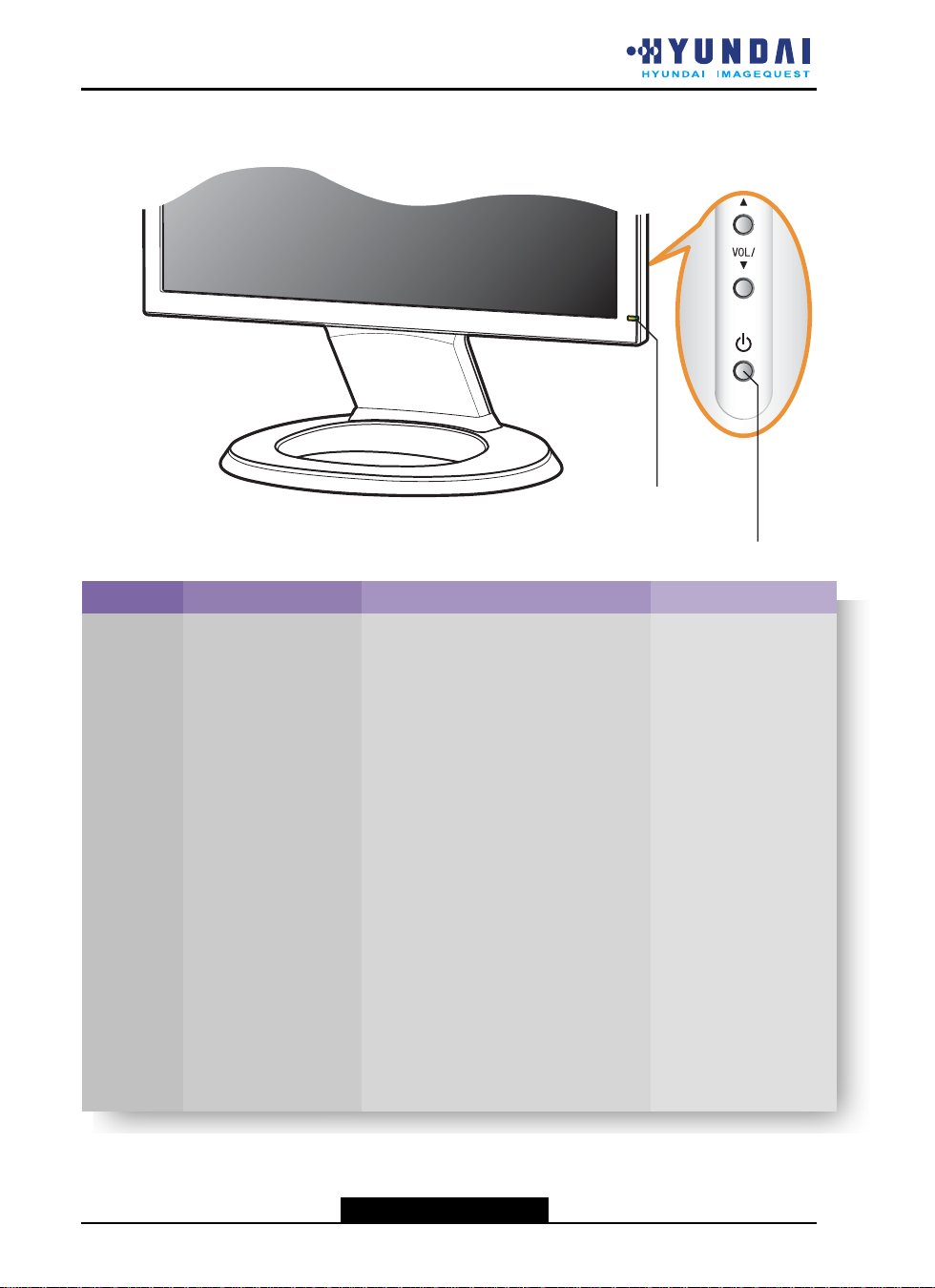
Control Description
Power Switch
LED Indecator
No.
1
2
3
4
5
6
7
8
9
10
11
12
13
14
Resolution
720
x
400
640 x 480
640 x 480
* 800 x 600
800 x 600
* 800 x 600
800 x 600
* 832 x 624
1024 x 768
1024 x 768
1024 x 768
*1152 x 864
1280 x 1024
1280 x 1024
Horizontal Frequency
31.5 KHz
31.5 KHz
37.5 KHz
35.2 KHz
37.9 KHz
48.1 KHz
46.9 KHz
49.7 KHz
48.4 KHz
56.5 KHz
60.0 KHz
67.5 KHz
63.9 KHz
80.0 KHz
Refresh rate
70 Hz
60 Hz
75 Hz
56 Hz
60 Hz
72 Hz
75 Hz
75 Hz
60 Hz
70 Hz
75 Hz
75 Hz
60 Hz
75 Hz
Front View
Support Modes
* Only B90A/B91A
(A70A/B71A/M17A/M17B/B90A/B91A)
--2--
B70A/B71A/M17A/M17B/B90A/B91A Technical Service Manual
ACTIVE (T4)
Front Porch
(T5)
Period (T1)
Sync Width (T2)
Back Porch (T3)
ACTIVE (T4)
Front Porch
(T5)
Period (T1)
Sync Width (T2)
Back Porch (T3)
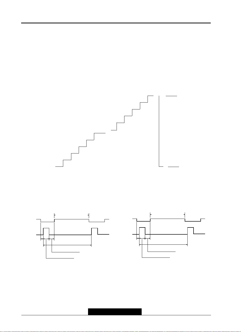
Video Input Signal
Recommended signal are shown below
•Video Signal
Video level : 0 to 700mV
Polarity : positive
Video Input : RGB separated
Sync input : H-Sync(TTL level)
•Waveform
Video input(R.G.B)
Analog level
V-Sync (TTL level)
• H-Sync
255
254
253
252
251
4
3
2
1
0
• Signal: 256 level gray
• Linear stepping:
(2.73mV ~ 256 Steps)
700mV
scale
0mV
• V-Sync
--3--
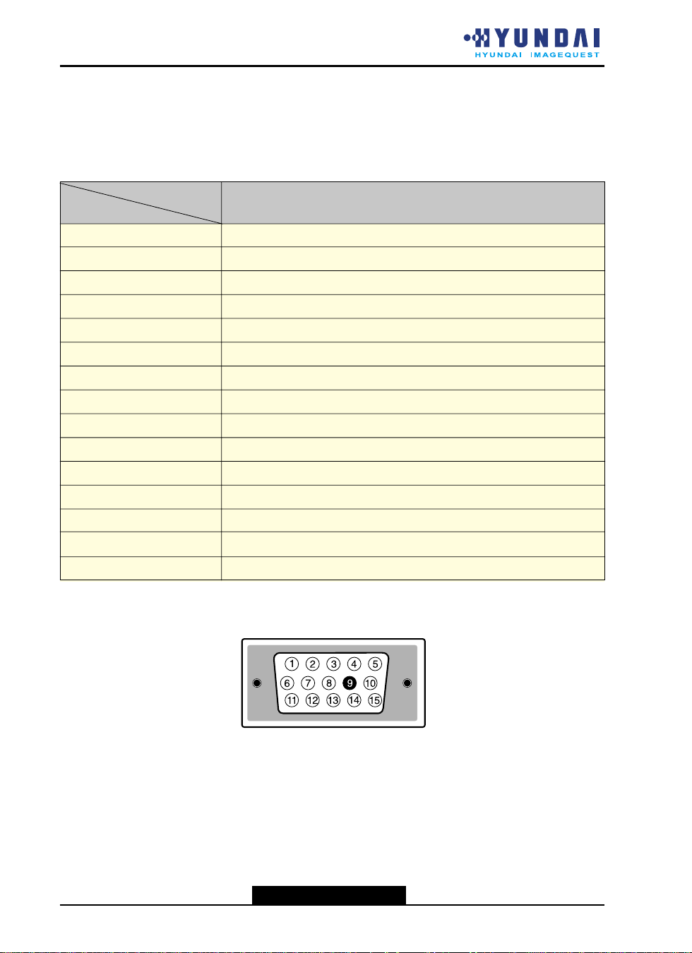
Video Input Terminal
A 15 Pin D-sub connector is used as the input signal connector
Pin and input signals are shown in the table below.
Pin Description
PIN NO.
1
2
3
4
5
6
7
8
9
10
11
12
13
14
15
SIGNAL
SEPARATE SYNC/
DDC 1/2B
RED
GREEN
BLUE
GND
RETURN
RED GROUND
GREEN GROUND
BLUE GROUND
N.C
LOGIC GROUND
GROUND
SDA
H-SYNC(TTL)
V-SYNC(VCLK)
SCL
D-Sub miniature connector
--4--
B70A/B71A/M17A/M17B/B90A/B91A Technical Service Manual
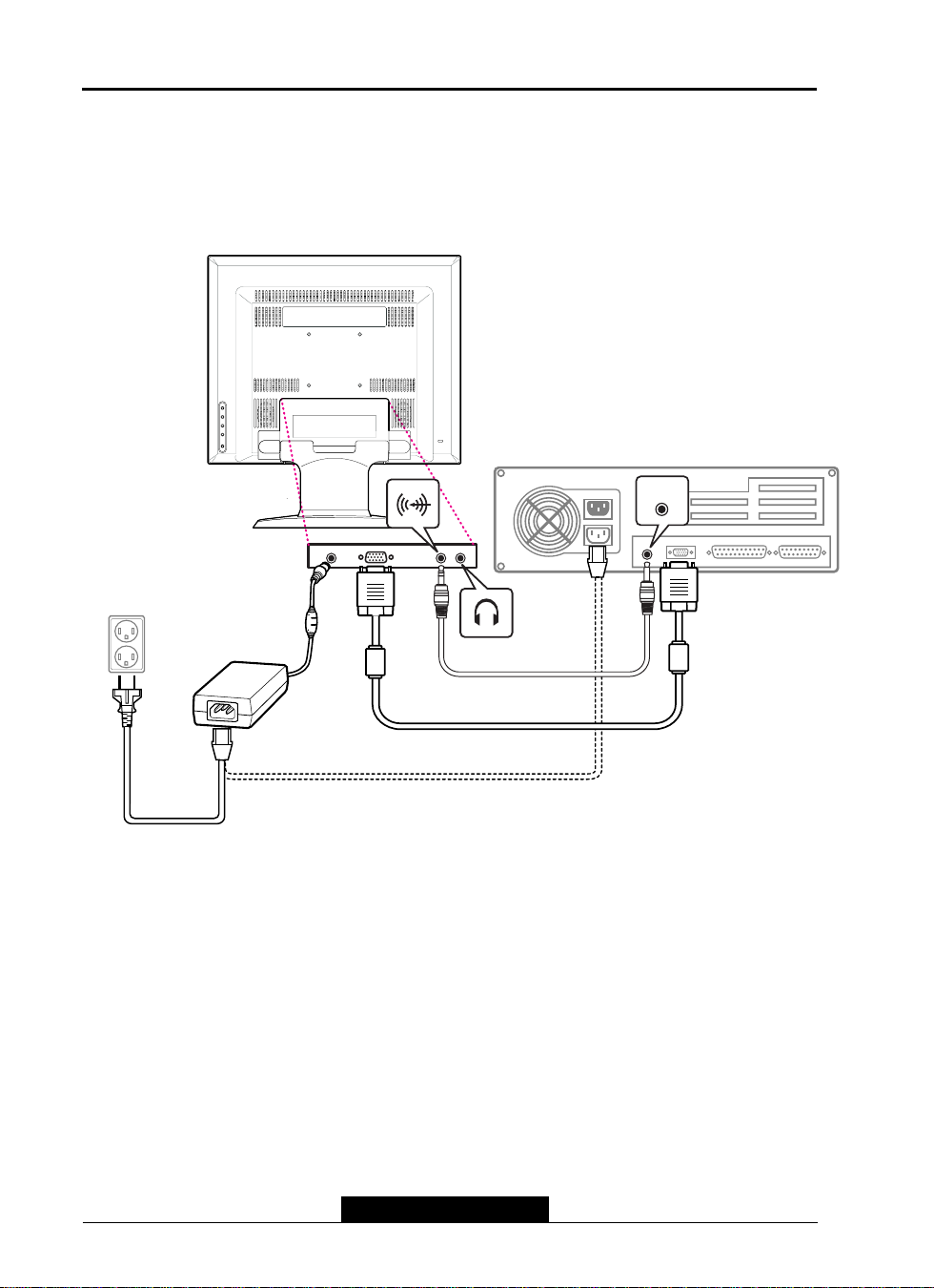
LINE OUT
* Audio System option Model
Connecting with External Equipment
Cautions
Be sure to turn off the power of your computer before connecting the monitor.
--5--

Theory of Operation
1. AC/DC INVERTER
Input voltage : DC 12V
Input current : 2.0A(Max)
Output current : 6.5mArms(TYP)
Frequency(switching) : 47KHz(Max)
Output power : 18W(TYP)
On/off control voltage : 5.0V
2. AC/DC ADATOR
This display device shall maintain the specified per formances in the range de scribed
below
Frequency : 50/60Hz
Voltage : 90 - 264Vac RMS
The following consumption requirments shall be met:
Power Consumption : 35W(typ)
Current consumption : < 1.0 Aac RMS
Output Specification:
+12V DC
3.3A Max
3. Audio System
This monitor has a audio system including two micro loudspeakers.
Each of two micro loudspeakers has a 2W(Max) output power.
This system also supports a headphone(earphone) output.
- Auto Signal Input : < 600mVp-p(Max.)
- Auto Amplifiers
2W+2W Amplifier with DC Volume Control (for two micro loudspeakers)
RL=8 @THD=10% Vcc=14V (min. 10V, max. 18V)
Dual-Audio Power Amplifier (for a headphone output)
RL=32
- Speaker
Micro Loudspeaker Spec.
Normal impedance 8
Resonance Freq. 550Hz +/- 110Hz at 1.0V
Freq. Range fo ~ 20KHz
Power Rating Normal 1.0W/Peak 2.0W
4. DPMS MODE
@THD=10% Vcc=4.5V (min. 1.8V, max. 15V)
15% at 1.0V 1.5KHz
Status
on
off
H-Sync
Pulse
No
Pulse
Signal
V-Sync Video
Active
Pulse
No
Pulse
Blank
Power
Consumption
35W(typ)
1W (TYP) 230V AC
--6--
Recovery
Time
-
Within 3
Sec
LED
Indicator
Green
Orange
B70A/B71A/M17A/M17B/B90A/B91A Technical Service Manual
1280 x 1024
H:63. 9 V:60.0
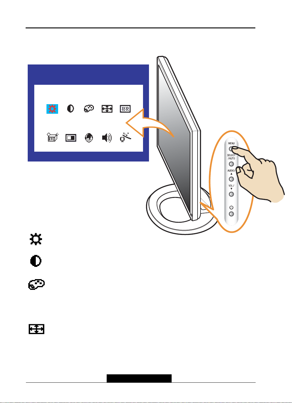
On Screen Controls & LED Indicator
The menu for screen setting adjustment is located in the OSD and can be viewed in one of
five languages OSD feature andmain funcrions are as follows:
1280x1024
H:63.9 V:60.0
BRIGHTNESSBRIGHTNESS
* Audio system Option Model
BRIGHTNESS
Adjust the brightness of the screen.
CONTRAST
Adjust the contrast of the screen.
COLOR CONTROL
Color temperature affects the tint of the image. With lower color
temperatures the image turns reddish and with higher temperatures
bluish.
There are three color settings available: Bluish, Reddish or USER. With
the USER setting you can set individual values for red, green and blue.
POSITION
H POSITION
Adjusts the horizontal position of the entire screen image.
V POSITION
Adjusts the vertical position of the entire screen image.
--7--
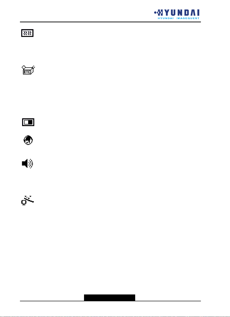
CLOCK PHASE
PHASE
Adjust the noise of the screen image.
CLOCK
Adjust the horizontal size of the entire screen image.
MISCELLANEOUS
RECALL
Recall the saved color data.
OSD TIMER
You can set the displayed time of OSD Menu window on the screen by using this
adjustment.
OSD POSITION
Adjust the OSD menu's horizontal or vertical position on the screen.
AUTO COLOR
Optimum color setting is auto programmed for user’s convenience.
LANGUAGE
You can select the language in which adjustment menus are displayed.
The following languages are available : English, French, German, Italian, Spanish,
Swedish, Finnish, Danish, Portuguese and Dutch(Option kiorea, Japanese chinese)
AUDIO
(Audio System Option Model)
VOLUME
Adjust the audio volume level.
AUDIO
This menu is used to choose audio on or off.
AUTO ADJUST
You can adjust the shape of screen automatically at the full screen pattern.
--8--

B70A/B71A/M17A/M17B/B90A/B91A Technical Service Manual
Getting Fine Picture
Step 1. At first Display, a full screen, such as, Window's background or "H" character should
be achieved by using Editor (ex: Notepad. exe)
Step 2. Adjust the screen to the center of the Display(LCD), by using the top and bottom
display controls. (i.e.Using V-Position Adjust menu)
Step 3. Adjust the screen to the center of the Display(LCD), by using the right and left
display controls. (i.e.Using Clock and H-Position adjust menu)
Step 4. Adjust the Clock-phase until the "H" Character displays clear.
Step 5. Using the Contrast. Brightness, and Color Control menu, set the color to your
preference.
Step 6. When you finish the adjustment, you can save your settings by pressing on the menu
until the OSD screen has disappeared.
Factory Setting & EEPROM Initialization Method
Factory Setting Method
- Connect the signal cable and power cable to the LCD monitor.
- Press Power switch with pressed MENU key.(Menu key + Power key).
- Then, a User can change the factory setting value in OSD menu.
- Save changed value and Turn off the power s/w.
- Turn on the power, adjust the screen.
--9--

1. No Video
Check The Adaptor NO
LED ? Green ?
YES
Check the Monitor
LED Green ?
YES
Check the Video Output Line YES OK
1. Full white Pattern or RGB
Garbage Video
NO NO
Check the Lamp! YES
Screen is dark in the lsghton condiforn ? YES
& You com see the faint Video int the darhroom
Power Saving mode
-> Check LED Color Green / Orange Toggle ?
NO Check the DC Input
NO
YES YES
Change The
Adaptor
CN3, DC 12V
U18 Output, DC 5V
Check the LVDS
Cable & Output ?
NO
NO H/V Sync
END
Chang the
INVERTER
Check MCU, Vcpu Voltage ? U5 #7 Pin
Signal Line ? U5 #41, # 42 Pin
END
Check the Voltage Line Replae & Check
12V Line con1 -> TO INVERTER 1. INVERTER
5V Line -> Vlcd, con4 NO 2 PCB Pattern
5v -> 3.3V, U 3 3 U 3
5V -> 1.8V, U 1 4 U 1
OK
Check Signal Line Waveform ? Change
1. Y2 Cvystal ? NO 1. LVDS Cable
2. CON4, LVDS Output ? 2. Panel
YES NO
END OK
OK
Check the Scaler, U4 & Replae
Check the MCU 45 <-> Scaler U4 WaveForm?
#19,20 #33, 34 Pin
--10--
OK
B70A/B71A/M17A/M17B/B90A/B91A Technical Service Manual
Specification
LCD Module
Input
SYNC
Display
Resolution
Video Bandwidth
User Control
OSD Control
Power Management
Plug & Play
Safety &
Regulation
Temperature
SIZE
Dot Pitch17" : 0.264mm , 19" : 0.294
Brightness
Response Time
Signal
Connector
H-Freq
V-Freq
Area(H)X(V)
Color
&
EMC
Safety
Ergonomi
Operating
Storage
17”/19" Viewable diagonal
300 cd/m
12m-sec (Typ)/8m-sec (Typ)
R.G.B Analog
15 pin D-SUB Connector
31.0kHz ~ 80.0kHz
56.0Hz ~ 75Hz
17" : 337.92X270.336mm, 19" : 376.32X301.056
16.2M Colors
1280 X 1024 @ 75Hz
135MHz
Contrast,Brightness, Position, Auto Color,
Clock Phase, Color Control, Language, Auto Adjust,
Miscellaneous, Audio Control, Audio(Option)
VESA DPMS Standard
VESA DDC 1/2B
FCC CLASS B , CE , VCCI
cULus, CE, TUV-GS, SEMKO
TCO’03/99
5 to 35 °C
- 5 to 45 °C
2
(TYP)
Humidity
Operating
Storage
unpacked
Weight
packed
Dimension(WXHXD mm)
* Specification is subject to change without notice for performance improvement.
30 to 80%(Non-condensing)
5 to 90%(Non-condensing)
17" : 3.2Kg, 19" : 3.5Kg
17" : 4.8Kg, 19" : 5.2Kg
17" : 374x401x200, 19" : 412x428x200
--11--
Critcal Parts Specification
1. LCD Module
Model
Display area
Drive system
Display color
Number of Pixel
Pixel arrangement
Pixel pitch
Weight
Conerast ratio
View angle Horizontal
Verticel
Response time
Luminance
Signal system
Supply voltage
Backlight Edge light
type
Power consumption
LCD Type/Vendor
B70/B71A/M70A/M70B
337.92(H)X20.336(V)mm
A-Si TFT
16.2M Colors
1280x1024
RGB vertical strip
0.264(H)X0.264(V)mm
2.1Kg
500:1
75 degree, 75 degree
75 degree, 60 degree
12ms(max)
300cd/m(typ)
Digital RGB signals, Sync
signals(H, V-Sync)
5.0V(Typ)
Four colt cathode flurescrnt
lamps With in-verter
2.8W(Typ) without B/L
LTM170EU-L21(SAMSUNG)
LTM 170E01-A5K3(LG)
B90A/B91A
376.32(H)X301.056(V)mm
A-Si TFT
16.7M Colors
1280x1024
RGB vertical strip
0.294(H)X0.294(V)mm
2.75Kg
700:1
75 degree, 75 degree
75 degree, 60 degree
8ms(Typ)
300cd/m(typ) / 250cd/m(typ)
Digital RGB signals, Sync
signals(H, V-Sync)
5.0V(Typ)
Four colt cathode flurescrnt
lamps With in-verter
2.8W(Typ) without B/L
LTM190EX-L01(SAMSUNG)
Lcd Module is a A-SI TFT active martix color liquid crystal compising
amorphous silicon TFT attached to each signal elecrode, a driving circuit
and a backlight. a built-in backlight display area contains 1280x1024
pixels and can display full color (16.2M/16.7M colors)
--12--
LTM 190E04-A4(LG)
B70A/B71A/M17A/M17B/B90A/B91A Technical Service Manual
2) CONNECTIONS
Physical interface is described as for the connector on module.
These connectors are capable of accommodating the following signals and will be following
components
Connector Name / Designation
Manufacturer
Type Parts Number
Mating Housing Part Number
Connector Name / Designation
Manufacturer
Type Parts Number
Mating Type Part Number
3) Signal Pin
Pin#
1
3
5
7
9
11
13
15
17
19
21
23
25
27
29
Signal Name
Rxo0-
Rxo1-
Rxo2-
GND
RxoC+
Rxo3+
RxEo+
RxE1-
GND
RxE2+
RxEC+
RxE3+
NC
NC
Power
Interface Connector / Interface card
JAE or compatible
FI-X30S-HF
FI-X30S-H
Lamp Connector / Backlight lamp
JST
BHR-04VS-1
SM04(4.0)B-BHS-1-TB
Pin#
2
4
6
8
10
12
14
16
18
20
22
24
26
28
30
Signal Name
Rxo0+
Rxo1+
Rxo2+
RxoC-
Rxo3-
RxE0-
GND
RxE1+
RxE2-
RxEC-
RxE3-
GND
NC
Power
Power
--13--
4) Signal Description
The module using a pair of LVDS receiver SN75LVDS82 (Texas Instruments) or compatible.
LVDS is a differential signal technology for LCD interface and high speed data transfer
device. Transmitter shall be SN75LVDS83(negative edge sampling)or compatible. The first
LVDS port(RxOxxx)transmots odd pixels while the second LVDS port(RxExxxx)transmits
even pixels.
PIN #
1
2
3
4
5
6
7
8
9
10
11
12
13
14
15
16
17
18
19
20
21
22
23
24
25
26
27
28
29
30
SIGNAL NAME
RxO0-
RxO0+
RxO1-
RxO1+
RxO2-
RxO2+
GND
RxOC-
RxOC+
RxO3-
RxO3+
RxE0-
RxE0+
GND
RxE1-
RxE1+
GND
RxE2-
RxE2+
RxEC-
RxEC+
RxE3-
RxE3+
GND
NC
NC
NC
POWER
POWER
POWER
Negative LVDS differential data input (odd data)
Positive LVDS differential data input (odd data)
Negative LVDS differential data input (odd data)
Positive LVDS differential data input (odd data)
Negative LVDS differential data input (odd data, H-Sync, V-Sync,DSPTMG)
Positive LVDS differential data input (odd data, H-Sync, V-Sync,DSPTMG)
Power Ground
Negative LVDS differential clock input (odd clock)
Positive LVDS differential clock input (odd clock)
Negative LVDS differential data input (odd data)
Positive LVDS differential data input (odd data)
Negative LVDS differential data input (Even clock)
Positive LVDS differential data input (Even data)
Power Ground
Positive LVDS differential data input (Even data)
Negative LVDS differential data input (Even data)
Power Ground
Negative LVDS differential data input (Even data)
Positive LVDS differential data input (Even data)
Negative LVDS differential clock input (Even clock)
Positive LVDS differential clock input (Even clock)
Negative LVDS differential data input (Even data)
Positive LVDS differential data input (Even data)
Power Ground
-
-
-
Power
Power
Power
DESCRIPTION
Note : Input signals of odd and even clock shall be the same timing.
LVDS DATA Name
DSP
V-S
H-S
Display Timing : When the signal is high, the pixel data shall be valid to be displayed
Vertical Sync : Both Positive and Negative polarity are acceptable
Horizontal Sync : Both Positive and Negative polarity are acceptable
DESCRIPTION
--14--
B70A/B71A/M17A/M17B/B90A/B91A Technical Service Manual
TSU16AL-LF
--15--

--16--
B70A/B71A/M17A/M17B/B90A/B91A Technical Service Manual
--17--

Pin Name
A0, A1 N.C.
A2 Device Address inputs
Vss Ground
SDA Data I/O
SCL Clock input
WP Write Protect
Vcc + 5 V or + 3 V
3.0 ABSOLUTE MAXIMUM RATINGS
Storage Temperature................................-65°C to + 125°C
Voltage with Respect to Ground.................-0.3
to + 6.5 V
NOTE: These are STRESS rating only. Appropriate conditions for operating these devices given elsewhere
may permanently damage the part. Prolonged exposure to maximum ratings may affect device reliability.
4.0 OPERATING CONDITIONS
Temperature under bias: MTV24C08/24LC08.......0°C to + 70°C
MTV24C08/24LC08-I.....-40°C to + 85°C
VCC
WP
SCL
SDA
A0
A1
A2
VSS
1
2
3
45
6
7
8
24C08
or
24LC08
TSSOP
VCC
WP
SCL
SDA
A0
A1
A2
VSS
VCC
WP
SCL
SDA
A0
A1
A2
VSS
1
2
3
4
8
7
6
5
1
2
3
45
6
7
8
Dual-In-Line
package
SO package
(M8)
24C08
or
24LC08
24C08
or
24LC08
24LC08
--18--
5.0 ELECTRICAL CHARACTERISTICS
DC ELECTRICAL CHARACTERISTICS
(Vcc =5V +/- 10% ,MTV24C08/24LC08
° F
Vcc =3V +/- 10% ,24LC08)
MTV24C08/
24LC08
24LC08
Units
Symbol Parameter Conditions
Min Max Min Max
ICC1
Operating Current
(Program)
SCL = 100KHZ
CMOS Input Levels
—10 — 8mA
ICC2
Operating Current
(Read)
SCL = 100KHZ
CMOS Input Levels
—2 —2mA
ISB
Standby Current SCL = SDA = 0 V
—10 —10
µA
IIL
Input Leakage VIN = 0 V to VCC
-1 +1 -1 +1
µA
IOL
Output Leakage VOUT = 0 V to Vcc
-1 +1 -1 +1
µA
VIL
Input Low Voltage
-0.1 0.8 -0.1
0.15 V
V
VIH
Input High Voltage
2
VCC +0.2 0.8VCCVCC+0.2
V
VOL1
Output Low Voltage IOL = 2.1mA TTL
— 0.4 — 0.4 V
VOH1
Output High Voltage IOH = -400uA TTL
2.4 — 2.4 — V
VOL2
Output Low Voltage IOL = 10uA CMOS
— 0.2 — 0.2 V
VOH2
Output High Voltage IOH = -10uA CMOS
VCC-0.2 — VCC-0.2
—V
VLK
Programming Command
Can Be Executed
Default — Default —V
6.0 SWITCHING CHACTERISTICS (Under Operating Conditions )
AC ELECTRICAL CHARACTERISTICS
(Vcc =5V +/- 10% , MTV24C08
° F
Vcc =3V +/- 10% ,24LC08)
(Vcc =5V +/- 10% , MTV24C08 Fast Mode)
MTV24C08/
24LC08
MTV24C08
(Fast Mode)
Parameter Symbol
Min Max Min Max
Units
Clock frequency Fscl 0 100 — 400 kHz
Clock high time Thigh 4000 — 600 — ns
Clock low time Tlow 4700 — 1200 — ns
SDA and SCL rise time Tr — 1000 — 300 ns
SDA and SCL fall time Tf — 300 — 300 ns
START condition hold time Thd:Sta 4000 — 600 — ns
START condition setup time Tsu:Sta 4700 — 600 — ns
Data input hold time Thd:Dat 0 — 0 — ns
Data input setup time Tsu:Dat 250 — 100 — ns
STOP condition setup time Tsu:Sto 4000 — 600 — ns
Output valid from clock Taa 300 3500 100 900 ns
Bus free time Tbuf 4700 — 1200 — ns
Data out hold time Tdh 300 — 50 — ns
Input filter spike suppression
(SDA and SCL pins)
Tsp — 100 — 50 ns
Write cycle time Twr — 10 — 10 ms
B70A/B71A/M17A/M17B/B90A/B91A Technical Service Manual
VCC Lockout Voltage
--19--
CC
CAPACITANCE TA= 25∞C , f=250KHZ
Symbol Parameter Max Units
COUT Output capacitance 5 pF
CIN Input capacitance 5 pF
A. C. Conditions of Test
Input Pulse Levels Vcc x 0.1 to Vcc x 0.9
Input Rise and Fall times 10 ns
Input and Output Timming level Vcc x 0.5
Output Load 1 TTL Gate and CL = 100pf
--20--

Features
•Low dropout voltage
•Load regulation: 0.05% typical
•Trimmed current limit
•On-chip thermal limiting
•Standard SOT-223, TO-263, and TO-252 packages
•
Three-terminal adjustable or fixed 1.8V, 2.5V, 2.85V, 3.3V, 5V
Applications
•Active SCSI terminators
•High efficiency linear regulators
•Post regulators for switching supplies
•Battery chargers
•5V to 3.3V linear regulators
•Motherboard clock supplies
Description
The RC1117 and RC1117-1.8V, 2.5, -2.85, -3.3 and -5 are low
dropout three-terminal regulators with 1A output current
capability. These de vices ha v e been optimized for lo w v oltage
where transient response and minimum input voltage are
critical. The 2.85V version is designed specifically to be
used in Active Terminators for SCSI bus.
Current limit is trimmed to ensure specified output current
and controlled short-circuit current. On-chip thermal limiting
provides protection against any combination of overload and
ambient temperatures that would create excessive junction
temperatures.
Unlike PNP type regulators where up to 10% of the output
current is wasted as quiescent current, the quiescent current
of the RC1117 flows into the load, increasing efficiency.
The RC1117 series regulators are available in the industrystandard SOT-223, TO-263 (D2PAK), and TO-252 (DPAK)
power packages.
Typical Applications
V
IN
= 3.3V V
IN
V
OUT
ADJ
1.5V, 1.8V at 1A
RC1117
10 F 2 2 F
R1
124
R2
24.9
V
IN
= 5V V
IN
V
OUT
GND
2.85V at 1A
RC1117-2.85
10 F
++
+
+
22 F
V
OUT
= V
REF
(1 + R2/R1) + I
Adj
• R2
RC1117
1A Adjustable/Fixed Low Dropout Linear Regulator
B70A/B71A/M17A/M17B/B90A/B91A Technical Service Manual
RC1117X2.5
--21--

Pin Assignments
*With package soldered to 0.5 square inch copper area over backside ground plane or internal po wer plane., JA can vary from
30°C/W to more than 50°C/W. Other mounting techniques may provide better thermal resistance than 30°C/W.
Absolute Maximum Ratings
Parameter Min. Max. Unit
V
IN
7.5 V
Operating Junction Temperature Range 0 125 C
Storage Temperature Range -65 150 C
Lead Temperature (Soldering, 10 sec.) 300 C
Front View
4-Lead Plastic SOT-223
JC
= 15 C/W*
3-Lead Plastic TO-252
JC
= 3 C/W*
Tab is
V
OUT
Tab is
V
OUT
1
ADJ/
GND
IN
23
3-Lead Plastic TO-263
JC
= 3 C/W*
Tab is
V
OUT
1
ADJ/
GND
INOUT
2 3
3
2
1
IN
OUT
ADJ/GND
--22--

Electrical Characteristics
Operating Conditions: VIN 7V, TJ = 25°C unless otherwise specified.
The denotes specifications which apply over the specified operating temperature range.
Notes:
1. See thermal regulation specifications for changes in output voltage due to heating effects. Load and line regulation are
measured at a constant junction temperature by low duty cycle pulse testing.
2. Line and load regulation are guaranteed up to the maximum power dissipation (18W). Power dissipation is determined by
input/output differential and the output current. Guaranteed maximum output power will not be available over the full input/
output voltage range.
3. RC1117 only.
Parameter Conditions Min. Typ. Max. Units
Reference Voltage, V
REF
3
1.5V (V
IN
- V
OUT
) 5.75V,
10mA I
OUT
1A
1.225
(-2%)
1.250 1.275
(+2%)
V
Output Voltage 10mA I
OUT
1A
RC1117-2.5, 4V V
IN
7V
RC1117-2.85, 4.35V V
IN
7V
RC1117-3.3, 4.8V V
IN
7V
RC1117-5, 6.5V V
IN
7V
2.450
2.793
3.234
4.900
2.5
2.85
3.3
5.0
2.550
2.907
3.366
5.100
V
V
V
V
Line Regulation
1,2
(V
OUT
+ 1.5V) VIN 7V, I
OUT
= 10mA 0.005 0.2 %
Load Regulation
1,2
(VIN – V
OUT
) = 2V, 10mA I
OUT
1A 0.05 0.5 %
Dropout Voltage V
REF
= 1%, I
OUT
= 1A 1.100 1.200 V
Current Limit (V
IN
– V
OUT
) = 2V 1.1 1.5 A
Adjust Pin Current, I
Adj
3
35 120 A
Adjust Pin Current Change
3
1.5V (VIN – V
OUT
) 5.75,
10mA I
OUT
1A
0.2 5 A
Minimum Load Current 1.5V (V
IN
– V
OUT
) 5.75 10 mA
Quiescent Current V
IN
= V
OUT
+ 1.25V 4 13 mA
Ripple Rejection f = 120Hz, C
OUT
= 22 F Tantalum,
(V
IN
– V
OUT
) = 3V, I
OUT
= 1A
60 72 dB
Thermal Regulation T
A
= 25 C, 30ms pulse 0.004 0.02 %/W
Temperature Stability 0.5 %
Long-Term Stability T
A
= 125 C, 1000hrs. 0.03 1.0 %
RMS Output Noise
(% of V
OUT
)
T
A
= 25 C, 10Hz f 10kHz 0.003 %
Thermal Resistance, Junction
to Case
SOT-223 15 C/W
TO-252, TO-263 3 C/W
Thermal Shutdown Junction Temperature 155 C
Thermal Shutdown
Hysteresis
10 C
B70A/B71A/M17A/M17B/B90A/B91A Technical Service Manual
1.764 1..8 1.836
--23--

RC1117-3.3
1A Adjustable/Fixed Low Dropout Linear Regulator
Features
•Low dropout voltage
•Load regulation: 0.05% typical
•Trimmed current limit
•On-chip thermal limiting
•Standard SOT-223, TO-263, and TO-252 packages
•Three-terminal adjustable or fixed 2.5V, 2.85V, 3.3V, 5V
Applications
•Active SCSI terminators
•High efficiency linear regulators
•Post regulators for switching supplies
•Battery chargers
•5V to 3.3V linear regulators
•Motherboard clock supplies
Typical Applications
RC1117
V
= 3.3V V
IN
10 F 2 2 F
IN
+
Description
The RC1117 and RC1117-2.5, -2.85, -3.3 and -5 are low
dropout three-terminal regulators with 1A output current
capability. These de vices ha v e been optimized for lo w v oltage
where transient response and minimum input voltage are
critical. The 2.85V version is designed specifically to be
used in Active Terminators for SCSI bus.
Current limit is trimmed to ensure specified output current
and controlled short-circuit current. On-chip thermal limiting
provides protection against any combination of overload and
ambient temperatures that would create excessive junction
temperatures.
Unlike PNP type regulators where up to 10% of the output
current is wasted as quiescent current, the quiescent current
of the RC1117 flows into the load, increasing efficiency.
The RC1117 series regulators are available in the industrystandard SOT-223, TO-263 (D2PAK), and TO-252 (DPAK)
power packages.
ADJ
V
OUT
R1
124
1.5V at 1A
+
= V
V
V
(1 + R2/R1) + I
OUT
REF
= 5V V
IN
10 F
R2
• R2
Adj
RC1117-2.85
GND
V
OUT
IN
++
24.9
22 F
--24--
2.85V at 1A

Pin Assignments
*With package soldered to 0.5 square inch copper area over backside ground plane or internal power plane., JA can vary from
30°C/W to more than 50°C/W. Other mounting techniques may provide better thermal resistance than 30°C/W.
Absolute Maximum Ratings
Parameter Min. Max. Unit
V
IN
7.5 V
Operating Junction Temperature Range 0 125 C
Storage Temperature Range -65 150 C
Lead Temperature (Soldering, 10 sec.) 300 C
Front View
4-Lead Plastic SOT-223
JC
= 15 C/W*
3-Lead Plastic TO-252
JC
= 3 C/W*
Tab is
V
OUT
Tab is
V
OUT
1
ADJ/
GND
IN
23
3-Lead Plastic TO-263
JC
= 3 C/W*
Tab is
V
OUT
1
ADJ/
GND
INOUT
2 3
3
2
1
IN
OUT
ADJ/GND
B70A/B71A/M17A/M17B/B90A/B91A Technical Service Manual
--25--

Electrical Characteristics
Operating Conditions: VIN 7V, TJ = 25°C unless otherwise specified.
The denotes specifications which apply over the specified operating temperature range.
Notes:
1. See thermal regulation specifications for changes in output voltage due to heating effects. Load and line regulation are
measured at a constant junction temperature by low duty cycle pulse testing.
2. Line and load regulation are guaranteed up to the maximum power dissipation (18W). Power dissipation is determined by
input/output differential and the output current. Guaranteed maximum output power will not be available over the full input/
output voltage range.
3. RC1117 only.
Parameter Conditions Min. Typ. Max. Units
Reference Voltage, V
REF
3
1.5V (V
IN
- V
OUT
) 5.75V,
10mA I
OUT
1A
1.225
(-2%)
1.250 1.275
(+2%)
V
Output Voltage 10mA I
OUT
1A
RC1117-2.5, 4V V
IN
7V
RC1117-2.85, 4.35V V
IN
7V
RC1117-3.3, 4.8V V
IN
7V
RC1117-5, 6.5V V
IN
7V
2.450
2.793
3.234
4.900
2.5
2.85
3.3
5.0
2.550
2.907
3.366
5.100
V
V
V
V
Line Regulation
1,2
(V
OUT
+ 1.5V) VIN 7V, I
OUT
= 10mA 0.005 0.2 %
Load Regulation
1,2
(VIN – V
OUT
) = 2V, 10mA I
OUT
1A 0.05 0.5 %
Dropout Voltage V
REF
= 1%, I
OUT
= 1A 1.100 1.200 V
Current Limit (V
IN
– V
OUT
) = 2V 1.1 1.5 A
Adjust Pin Current, I
Adj
3
35 120 A
Adjust Pin Current Change
3
1.5V (VIN – V
OUT
) 5.75,
10mA I
OUT
1A
0.2 5 A
Minimum Load Current 1.5V (V
IN
– V
OUT
) 5.75 10 mA
Quiescent Current V
IN
= V
OUT
+ 1.25V 4 13 mA
Ripple Rejection f = 120Hz, C
OUT
= 22 F Tantalum,
(V
IN
– V
OUT
) = 3V, I
OUT
= 1A
60 72 dB
Thermal Regulation T
A
= 25 C, 30ms pulse 0.004 0.02 %/W
Temperature Stability 0.5 %
Long-Term Stability T
A
= 125 C, 1000hrs. 0.03 1.0 %
RMS Output Noise
(% of V
OUT
)
T
A
= 25 C, 10Hz f 10kHz 0.003 %
Thermal Resistance, Junction
to Case
SOT-223 15 C/W
TO-252, TO-263 3 C/W
Thermal Shutdown Junction Temperature 155 C
Thermal Shutdown
Hysteresis
10 C
--26--

B70A/B71A/M17A/M17B/B90A/B91A Technical Service Manual
SI4435
HEXFETÆ Power MOSFET
-
Ultra Low On-Resistance
P-Channel MOSFET
-
Surface Mount
-
-
Available in Tape & Reel
Description
These P-channel HEXFETÆ Power MOSFETs from
International Rectifier utilize advanced processing
techniques to achieve the extremely low on-resistance per
silicon area. This benefit provides the designer with an
extremely efficient device for use in battery and load
management applications..
The SO-8 has been modified through a customized
leadframe for enhanced thermal characteristics and
multiple-die capability making it ideal in a variety of power
applications. With these improvements, multiple devices
can be used in an application with dramatically reduced
board space. The package is designed for vapor phase,
infrared, or wave soldering techniques.
S
S
S
1
2
3
4
Top View
8
7
6
5
PD- 93768A
Si4435DY
A
D
V
= -30V
R
DS(on)
DSS
= 0.020Ω
D
D
DG
SO-8
Absolute Maximum Ratings
V
DS
I
@ TA = 25∞C Continuous Drain Current, VGS @ -10V -8.0
D
I
@ TA= 70∞C Continuous Drain Current, VGS @ -10V -6.4 A
D
I
DM
P
= 25∞C Power Dissipation 2.5
D @TA
PD @TA = 70∞C Power Dissipation 1.6
V
GS
T
J, TSTG
Drain- Source Voltage -30 V
Pulsed Drain Current Å -50
Linear Derating Factor 0.02 W/ C
Gate-to-Source Voltage ± 20 V
Junction and Storage Temperature Range -55 to + 150 C
Parameter Max. Units
Thermal Resistance
R
θJA
Maximum Junction-to-AmbientÉ 50 C/W
Parameter Max. Units
--27--
W
o
o
o

Si4435DY
Parameter Min. Typ. Max. Units Conditions
I
S
Continuous Source Current MOSFET symbol
(Body Diode) showing the
I
SM
Pulsed Source Current integral reverse
(Body Diode) Å p-n junction diode.
V
SD
Diode Forward Voltage ñññ ñññ -1.2 V TJ = 25∞C, IS = -2.5A, VGS = 0V Ç
t
rr
Reverse Recovery Time ñññ 34 51 ns TJ = 25∞C, IF = -2.5A
Q
rr
Reverse Recovery Charge ñññ 33 50 nC di/dt = -100A/µs Ç
Source-Drain Ratings and Characteristics
A
-50
ñññ
ñññ
ñññ
-2.5
ñññ
S
D
G
Å Repetitive rating; pulse width limited by
max. junction temperature.
Notes:
Ç Pulse width ≤ 300µs; duty cycle ≤ 2%.
É Surface mounted on FR-4 board, t ≤ 5sec.
Parameter Min. Typ. Max. Units Conditions
V
(BR)DSS
Drain-to-Source Breakdown Voltage -30 ñññ ñññ V VGS = 0V, ID = -250µA
∆V
(BR)DSS
/∆T
J
Breakdown Voltage Temp. Coefficient ñññ-0.019 ñññ V/∞C Reference to 25∞C, ID = -1mA
ñññ0.015 0.020 V
GS
= -10V, ID = -8.0A Ç
ñññ0.026 0.035 VGS = -4.5V, ID = -5.0A Ç
V
GS(th)
Gate Threshold Voltage -1.0 ñññ ñññ V VDS = VGS, ID = -250µA
g
fs
Forward Transconductance ñññ 11 ñññ S VDS = -15V, ID = -8.0A
ñññ ñññ -10 VDS = -24V, VGS = 0V
ñññ ñññ -10 V
DS
= -15V, VGS = 0V, TJ = 70∞C
Gate-to-Source Forward Leakage ñññ ñññ -100 V
GS
= -20V
Gate-to-Source Reverse Leakage ñññ ñññ 100 V
GS
= 20V
Q
g
Total Gate Charge ñññ 40 60 ID = -4.6A
Q
gs
Gate-to-Source Charge ñññ 7.1 ñññ nC VDS = -15V
Q
gd
Gate-to-Drain ("Miller") Charge ñññ 8.0 ñññ VGS = -10V Ç
t
d(on)
Turn-On Delay Time ñññ 16 24 VDD = -15V, VGS = -10V Ç
t
r
Rise Time ñññ 76 110 ID = -1.0A
t
d(off)
Turn-Off Delay Time ñññ 130 200 RG = 6.0Ω
t
f
Fall Time ñññ 90 140 RD = 15Ω
C
iss
Input Capacitance ñññ 2320 ñññ VGS = 0V
C
oss
Output Capacitance ñññ 390 ñññ pF VDS = -15V
C
rss
Reverse Transfer Capacitance ñññ 270 ñññ É = 1.0kHz
Electrical Characteristics @ TJ = 25∞C (unless otherwise specified)
I
GSS
µA
Ω
R
DS(on)
Static Drain-to-Source On-Resistance
I
DSS
Drain-to-Source Leakage Current
nA
ns
--28--

B70A/B71A/M17A/M17B/B90A/B91A Technical Service Manual
UTC 7496L
2W+2W AMPLIFIER WITH DC VOLUME CONTROL
2W+2W OUTPUT POWER
R
= 8Ω @THD = 10% VCC = 14V
L
ST-BY AND MUTE FUNCTIONS
LOW TURN-ON TURN-OFF POP NOISE
LINEAR VOLUME CONTROL DC COUPLED
WITH POWER OP. AMP.
NO BOUCHEROT CELL
NO ST-BY RC INPUT NETWORK
SINGLE SUPPLY RANGING UP TO 15V
SHORT CIRCUIT PROTECTION
THERMAL OVERLOAD PROTECTION
INTERNALLY FIXED GAIN
SOFT CLIPPING
VARIABLE OUTPUT AFTER VOLUME CON-
TROL CIRCUIT
POWERDIP (14+3+3) PACKAGE
DESCRIPTION
The TDA7496L is a stereo 2W+2W class AB
power amplifier assembled in the @ Powerdip
14+3+3 package, specially designed for high
quality sound, TV and Monitor applications.
Features of the TDA7496L include linear volume
control, Stand-by and mute functions.
ORDERING NUMBER:
Powerdip (14+3+3)
TDA7496L
BLOCK DIAGRAM
GND
INR
470nF
INL
470nF
SVR 10
470µF
1,2,3,13,
18,19,20
9
4
VOLUME
30K
VOLUME
65
VOLUME
100nF
VAROUT_R
7
PROTECTIONS
VAROUT_L
300K
15,16
+
OP AMP
MUTE/STBY
+
-30K
OP AMP
+5V
V
S
1000µF
14
OUTR
S1 ST-BY
60K
11
12
17
D97AU596A
STBY
MUTE
OUTL
10K
1µF
1000µF
S2 MUTE
+5V
S_GND
+5V
--29--

GND
GND
GND
INL
VAROUT_L
VAROUT_R
VOLUME
N.C.
INR
1
3
2
4
5
6
7
8
9 MUTE
GND
OUTR
V
S
V
S
OUTL
GND
GND
GND20
19
18
17
16
14
15
13
12
D97AU597A
SVR 10 STBY11
PIN CONNECTION
THERMAL DATA
Symbol Parameter Value Unit
R
th j-pins
Thermal Resistance Junction-pins max. 15 ∞C/W
R
th j-amb
(*) Thermal Resistance Junction-ambient max. 50 ∞C/W
(*) Mounted on PCB with no heatsink
ELECTRICAL CHARACTERISTICS
(Refer to the test circuit V
S
= 14V; RL = 8Ω, Rg = 50Ω, T
amb
= 25∞C).
Symbol Parameter Test Condition Min. Typ. Max. Unit
V
S
Supply Voltage Range 10 18 V
I
q
Total Quiescent Current 25 50 mA
DCV
OS
Output DC Offset Referred to
SVR Potenial
No Input Signal 200 mV
V
O
Quiescent Output Voltage 7 V
P
O
Output Power THD = 10%; RL = 8Ω; 1 .6 2 W
THD = 1%; R
L
= 8Ω; 1 .3 W
THD Total Harmonic Distortion G
V
= 30dB; PO = 1W; f = 1KHz; 0.4 %
I
peak
Output Peak Current (internally limited) 0.7 0.9 A
V
in
Input Signal 2.8 Vrms
G
V
Closed Loop Gain Vol Ctrl > 4.5V 28.5 30 31.5 dB
G
vLine
Monitor Out Gain Vol Ctrl > 4.5V; Zload > 30KΩ -1.5 0 1.5 dB
A
Min VOL
Attenuation at Minimum Volume Vol Ctrl < 0.5V 80 dB
BW 0.6 MHz
ABSOLUTE MAXIMUM RATIN GS
Symbol Parameter Value Unit
V
S
DC Supply Voltage 26 V
V
IN
Maximum Input Voltage 8 Vpp
P
tot
Total Power Dissipation (T
case
= 60∞C) 6 W
T
amb
Ambient Operating Temperature 0 to 70 ∞C
T
stg
, T
j
Storage and Junction Temperature -40 to 150 ∞C
V
6
Volume CTRL DC voltage 7 V
0 4 8 12 Area(cm2)
30
40
50
60
R
thj-a
(∞C/W)
D97AU675
COPPER AREA 35µ
THICKNESS
PC BOARD
Rth with "on board" Square Heatsink vs. copper area.
--30--
ELECTRICAL CHARACTERISTICS
(continued)
Symbol Parameter Test Condition Min. Typ. Max. Unit
e
N
Total Output Noise f = 20Hz to 22KHz
Play, max volume
500 800 µV
f = 20Hz to 22KHz
Play, max attenuation
100 250 µV
f = 20Hz to 22KHz
Mute
60 150 µV
SR Slew Rate 5 8 V/µs
R
i
Input Resistance 22.5 30 KΩ
R
Var Out
Variable Output Resistance 30 100 Ω
R
load Var Out
Variable Output Load 2 KΩ
SVR Supply Voltage Rejection f = 1kHz; max volume
C
SVR
= 470µF; V
RIP
= 1V
rms
35 39 dB
f = 1kHz; max attenuation
C
SVR
= 470µF; V
RIP
=1V
rms
55 65 dB
T
M
Thermal Muting 150 ∞C
T
s
Thermal Shut-down 160 ∞C
MUTE STAND-BY & INPUT SELECTION FUNCTIONS
V
ST ON
Stand-by ON Threshold 3.5 V
V
ST OFF
Stand-by OFF Threshold 1.5 V
V
M ON
Mute ON Threshold 3.5 V
V
M OFF
Mute OFF Threshold 1.5 V
I
qST-BY
Quiescent Current @ Stand-by 0.6 1 mA
A
MUTE
Mute Attenuation 50 65 dB
I
stbyBIAS
Stand-by bias current Stand by on V
ST-BY
= 5V
V
MUTE
= 5V
80 µA
µA
Play or Mute -20 -5 µA
I
muteBIAS
Mute bias current Mute 1 5 µA
Play 0.2 2 µA
APPLICATION SUGGESTIONS
The recommended values of the external components are those shown on the application circuit of figure 1A. Different values can be used, the following table can help the designer.
COMPONENT
SUGGESTION
VALUE
PURPOSE
LARGER THAN
SUGGESTION
SMALLER THAN
SUGGESTION
R1 300K Volume control
circuit
Larger volume regulation
time
Smaller volume regulation
time
R2 10K Mute time constant Larger mute on/off time Smaller mute on/off time
P1 50K Volume control
circuit
C1 1000µF Supply voltage
bypass
Danger of oscillation
C2 470nF Input DC decoupling Lower low frequency cutoff Higher low frequency cutoff
C3 470nF Input DC decoupling Lower low frequency cutoff Higher low frequency cutoff
C4 470µF Ripple rejection Better SVR Worse SVR
C5 100nF Volume control time
costant
Larger volume regulation
time
Smaller volume regulation
time
C6 1000µF Output DC
decoupling
Lower low frequency cutoff Higher low frequency cutoff
C7 1µF Mute time costant Larger mute on/off time Smaller mute on/off time
C8 1000µF Output DC
decoupling
Lower low frequency cutoff Higher low frequency cutoff
C9 100nF Supply voltage
bypass
Danger of oscillation
B70A/B71A/M17A/M17B/B90A/B91A Technical Service Manual
--31--

NCP1117/NCP1117
NCP1117, NCV1117
1.0 A Low-Dropout Positive
Fixed and Adjustable
Voltage Regulators
The NCP1117 series are low dropout positive voltage regulators that
are capable of providing an output current that is in excess of 1.0 A
with a maximum dropout voltage of 1.2 V at 800 mA over
temperature. This series contains eight fixed output voltages of 1.5 V,
1.8 V, 2.0 V, 2.5 V, 2.85 V, 3.3 V, 5.0 V, and 12 V that have no
minimum load requirement to maintain regulation. Also included is an
adjustable output version that can be programmed from 1.25 V to
18.8 V with two external resistors. On chip trimming adjusts the
reference/output voltage to within +1.0% accuracy. Internal protection
features consist of output current limiting, safe operating area
compensation, and thermal shutdown. The NCP1117 series can
operate with up to 20 V input. Devices are available in SOT-223 and
DPAK packages.
Features
ωOutput Current in Excess of 1.0 A
ω1.2 V Maximum Dropout Voltage at 800 mA Over Temperature
ωFixed Output Voltages of 1.5 V, 1.8 V, 2.0 V, 2.5 V, 2.85 V, 3.3 V,
5.0 V, and 12 V
ωAdjustable Output Voltage Option
ωNo Minimum Load Requirement for Fixed Voltage Output Devices
ωReference/Output Voltage Trimmed to +1.0%
ωCurrent Limit, Safe Operating and Thermal Shutdown Protection
ωOperation to 20 V Input
ωNCV Prefix for Automotive and Other Applications Requiring Site
and Control Changes
ωPb-Free Packages are Available
Applications
ωConsumer and Industrial Equipment Point of Regulation
ωActive SCSI Termination for 2.85 V Version
ωSwitching Power Supply Post Regulation
ωHard Drive Controllers
ωBattery Chargers
10
F
1
2
Output
10
F
3
Input
NCP1117
XTXX
++
Figure 1. Fixed
Output Regulator
10
F
1
2
Output
10
F
3
Input
NCP1117
XTA
++
Figure 2. Adjustable
Output Regulator
22
F
1
2
10
F
3
NCP1117
XT285
++
110
110
110
110
4.75 V
to
5.25 V
+
18 to 27
Lines
Figure 3. Active SCSI Bus Terminator
TYPICAL APPLICATIONS
SOT-223
ST SUFFIX
CASE 318H
1
3
DPAK
DT SUFFIX
CASE 369C
Pin: 1. Adjust/Ground
2. Output
3. Input
1
3
Heatsink tab is connected to Pin 2.
See detailed ordering and shipping information in the package
dimensions section on pages 11 and 12 of this data sheet.
ORDERING INFORMATION
See general marking information in the device marking
section on page 13 of this data sheet.
DEVICE MARKING INFORMATION
1 23
123
Tab
Tab
(Top View)
(Top View)
http://onsemi.com
--32--
B70A/B71A/M17A/M17B/B90A/B91A Technical Service Manual
NCP1117, NCV1117
MAXIMUM RATINGS
Rating Symbol Value Unit
Input Voltage (Note 1) V
in
20 V
Output Short Circuit Duration (Notes 2 and 3) - Infinite Power Dissipation and Thermal Characteristics
Case 318H (SOT-223)
Power Dissipation (Note 2)
Thermal Resistance, Junction-to-Ambient, Minimum Size Pad
Thermal Resistance, Junction-to-Case
Case 369A (DPAK)
Power Dissipation (Note 2)
Thermal Resistance, Junction-to-Ambient, Minimum Size Pad
Thermal Resistance, Junction-to-Case
P
D
R
JA
R
JC
P
D
R
JA
R
JC
Internally Limited
160
15
Internally Limited
67
6.0
W
5C/W
5C/W
W
5C/W
5C/W
Maximum Die Junction Temperature Range T
J
-55 to 150 5C
Storage Temperature Range T
stg
-65 to 150 5C
Operating Ambient Temperature Range
NCP1117
NCV1117
T
A
0 to +125
-40 to +125
5C
Maximum ratings are those values beyond which device damage can occur. Maximum ratings applied to the device are individual stress limit
values (not normal operating conditions) and are not valid simultaneously. If these limits are exceeded, device functional operation is not implied,
damage may occur and reliability may be affected.
1. This device series contains ESD protection and exceeds the following tests:
Human Body Model 2000 V per MIL-STD-883, Method 3015.
Machine Model Method 200 V.
2. Internal thermal shutdown protection limits the die temperature to approximately 1755C. Proper heatsinking is required to prevent activation.
The maximum package power dissipation is:
P
D
T
J(max)TA
R
JA
3. The regulator output current must not exceed 1.0 A with Vin greater than 12 V.
--33--
NCP1117, NCV1117
ELECTRICAL CHARACTERISTICS (C
in
= 10 F, C
out
= 10 F, for typical value TA = 255C, for min and max values TA is the
operating ambient temperature range that applies unless otherwise noted. (Note 6)
Characteristic
Symbol Min Typ Max Unit
Reference Voltage, Adjustable Output Devices
(V
in±Vout
= 2.0 V, I
out
= 10 mA, TA = 255C)
(V
in±Vout
= 1.4 V to 10 V, I
out
= 10 mA to 800 mA) (Note 6)
V
ref
1.238
1.225
1.25-1.262
1.270
V
Output Voltage, Fixed Output Devices
1.5 V (V
in
= 3.5 V, I
out
= 10 mA, TA = 25 5C)
(V
in
= 2.9 V to 11.5 V, I
out
= 0 mA to 800 mA) (Note 6)
1.8 V (V
in
= 3.8 V, I
out
= 10 mA, TA = 25 5C)
(V
in
= 3.2 V to 11.8 V, I
out
= 0 mA to 800 mA) (Note 6)
2.0 V (V
in
= 4.0 V, I
out
= 10 mA, TA = 25 5C)
(V
in
= 3.4 V to 12 V, I
out
= 0 mA to 800 mA) (Note 6)
2.5 V (V
in
= 4.5 V, I
out
= 10 mA, TA = 25 5C)
(V
in
= 3.9 V to 10 V, I
out
= 0 mA to 800 mA,) (Note 6)
2.85 V (V
in
= 4.85 V, I
out
= 10 mA, TA = 25 5C)
(V
in
= 4.25 V to 10 V, I
out
= 0 mA to 800 mA) (Note 6)
(V
in
= 4.0 V, I
out
= 0 mA to 500 mA) (Note 6)
3.3 V (V
in
= 5.3 V, I
out
= 10 mA, TA = 25 5C)
(V
in
= 4.75 V to 10 V, I
out
= 0 mA to 800 mA) (Note 6)
5.0 V (V
in
= 7.0 V, I
out
= 10 mA, TA = 25 5C)
(V
in
= 6.5 V to 12 V, I
out
= 0 mA to 800 mA) (Note 6)
12 V (V
in
= 14 V, I
out
= 10 mA, TA = 25 5C)
(V
in
= 13.5 V to 20 V, I
out
= 0 mA to 800 mA) (Note 6)
V
out
1.485
1.470
1.782
1.755
1.970
1.960
2.475
2.450
2.821
2.790
2.790
3.267
3.235
4.950
4.900
11.880
11.760
1.500
-
1.800
-
2.000
-
2.500
-
2.850
-
-
3.300
-
5.000
-
12.000
-
1.515
1.530
1.818
1.845
2.030
2.040
2.525
2.550
2.879
2.910
2.910
3.333
3.365
5.050
5.100
12.120
12.240
V
Line Regulation (Note 4)
Adjustable (V
in
= 2.75 V to 16.25 V, I
out
= 10 mA)
Reg
line
- 0.04 0.1
%
1.5 V (Vin = 2.9 V to 11.5 V, I
out
= 0 mA)
1.8 V (V
in
= 3.2 V to 11.8 V, I
out
= 0 mA)
2.0 V (V
in
= 3.4 V to 12 V, I
out
= 0 mA)
2.5 V (V
in
= 3.9 V to 10 V, I
out
= 0 mA)
2.85 V (V
in
= 4.25 V to 10 V, I
out
= 0 mA)
3.3 V (V
in
= 4.75 V to 15 V, I
out
= 0 mA)
5.0 V (V
in
= 6.5 V to 15 V, I
out
= 0 mA)
12 V (V
in
= 13.5 V to 20 V, I
out
= 0 mA)
-
-
-
-
-
-
-
-
0.3
0.4
0.5
0.5
0.8
0.8
0.9
1.0
1.0
1.0
2.5
2.5
3.0
4.5
6.0
7.5
mV
Load Regulation (Note 4)
Adjustable (I
out
= 10 mA to 800 mA, Vin = 4.25 V)
Reg
line
- 0.2 0.4
%
1.5 V (I
out
= 0 mA to 800 mA, Vin = 2.9 V)
1.8 V (I
out
= 0 mA to 800 mA, Vin = 3.2 V)
2.0 V (I
out
= 0 mA to 800 mA, Vin = 3.4 V)
2.5 V (I
out
= 0 mA to 800 mA, Vin = 3.9 V)
2.85 V (I
out
= 0 mA to 800 mA, Vin = 4.25 V)
3.3 V (I
out
= 0 mA to 800 mA, Vin = 4.75 V)
5.0 V (I
out
= 0 mA to 800 mA, Vin = 6.5 V)
12 V (I
out
= 0 mA to 800 mA, Vin = 13.5 V)
-
-
-
-
-
-
-
-
2.3
2.6
3.0
3.3
3.8
4.3
6.7
16
5.5
6.0
6.0
7.5
8.0
10
15
28
mV
Dropout Voltage (Measured at V
out
- 100 mV)
(I
out
= 100 mA)
(I
out
= 500 mA)
(I
out
= 800 mA)
Vin-V
out
-
-
-
0.95
1.01
1.07
1.10
1.15
1.20
V
Output Current Limit (Vin-V
out
= 5.0 V, TA = 255C, Note 5) I
out
1000 1500 2200 mA
4. Low duty cycle pulse techniques are used during testing to maintain the junction temperature as close to ambient as possible.
5. The regulator output current must not exceed 1.0 A with V
in
greater than 12 V.
6. NCP1117: T
low
= 05C , T
high
= 1255C
NCV1117: T
low
= -40 5C, T
high
= 1255C
--34--

B70A/B71A/M17A/M17B/B90A/B91A Technical Service Manual
NCP1117, NCV1117
ELECTRICAL CHARACTERISTICS (C
in
= 10 F, C
out
= 10 F, for typical value TA = 255C, for min and max values TA is the
operating ambient temperature range that applies unless otherwise noted. (Note 7)
Characteristic
Symbol Min Typ Max Unit
Minimum Required Load Current for Regulation, Adjustable Output Devices
(V
in
= 15 V)
I
L(min)
- 0.8 5.0 mA
Quiescent Current
1.5 V (V
in
= 11.5 V)
1.8 V (V
in
= 11.8 V)
2.0 V (V
in
= 12 V)
2.5 V (V
in
= 10 V)
2.85 V (V
in
= 10 V)
3.3 V (V
in
= 15 V)
5.0 V (V
in
= 15 V)
12 V (V
in
= 20 V)
I
Q
-
-
-
-
-
-
-
-
3.6
4.2
4.5
5.2
5.5
6.0
6.0
6.0
10
10
10
10
10
10
10
10
mA
Thermal Regulation (TA = 255C, 30 ms Pulse) - 0.01 0.1 %/W
Ripple Rejection (Vin-V
out
= 6.4 V, I
out
= 500 mA, 10 Vpp 120 Hz Sinewave)
Adjustable
1.5 V
1.8 V
2.0 V
2.5 V
2.85 V
3.3 V
5.0 V
12 V
RR
67
66
64
64
62
62
60
57
50
73
72
70
70
68
68
64
61
54
-
-
-
-
-
-
-
-
-
dB
Adjustment Pin Current (Vin = 11.25 V, I
out
= 800 mA) I
adj
- 52 120 A
Adjust Pin Current Change
(V
in-Vout
= 1.4 V to 10 V, I
out
= 10 mA to 800 mA)
I
adj
- 0.4 5.0 A
Temperature Stability S
T
- 0.5 - %
Long Term Stability (TA = 255C, 1000 Hrs End Point Measurement) S
t
- 0.3 - %
RMS Output Noise (f = 10 Hz to 10 kHz) N - 0.003 - %V
out
7. NCP1117: T
low
= 05C , T
high
= 1255C
NCV1117: T
low
= -40 5C, T
high
= 1255C
--35--

BLACK DIAGEAM
MODEL NAME : B70A/B71A/BM17A/M17B/B90A/B91A
Analog R.G.B
12 -> 3.3A
24MHz
Scaler
(TSU16AL)
MCU
LVDS
17/19"
LCD
PANEL
INVERTER
+12V
AUDIO
SPK

B70A/B71A/B90A/B91A/M17A/M17B PART LIST
PART NO PART NUMBER DESCRIPTION LOCATION
E4205025501
B70A/B90A
(Schematic)
1
E4208627201
2
E4208527201
3
E4208427211
4
CC7FCA1H220J
5
RK1JC0T0101J
6
RK1JC0T0102J
7
RK1JC0T0103J
8
RK1JC0T0105J
9
RK1JC0T0151J
10
RK1JC0T0471J
11
RK1JC0T0472J
12
TT2N3904D
13
2014790003
14
2121040045
15
MAIN ASSY/TSU16AL,B70A EXP
PCBA MAIN(TM),B70A
PCBA MAIN(MM),B70A
PCBA MAIN(AM),B70A
CAP-CC,22PF 50V J 1608
RES-C,100 0.063W J 1608
RES-C,1K 0.063W J 1608
RES-C,10K 0.063W J 1608
RES-C,1M 0.063W J 1608
RES CHIP 150 J 0.063W 1608
RES-C,470 0.063W J 1608
RES-C,4.7K 0.063W J 1608
TR,SMD 2N3904D TAPPING
CAP-AL-C,4.7UF 25V M 4052
CAP-C-C,0.1UF 50V Z Y5V 1608
C159
C63
C65
R11
R14
R19
R22
R24
R29
R34
R52
R72
R73
R8
R4
R55
R68
R69
R42
R47
R61
R45
R54
R56
R57
R59
R60
R64
R65
R2
R36
R44
R49
R50
R53
R83
Q2
C61
C12
C14
C15
C18

PART NO PART NUMBER DESCRIPTION LOCATION
C221
B70A/B90A
(Schematic)
2122210028
16
2124710037
17
2125090017
18
2594701009
19
2600008008
20
2602000010
21
2602009011
22
2602202015
23
2603900008
24
2607500012
25
2607509010
26
CAP-C-C,220PF 50V J COG 1608
CAP-C-C,470PF 50V J COG 1608
CAP-C-C,5PF 50V J COG 1608
RES-C-NET,4.7K 0.063W J 3216
RES-C,0 0.125W J 3216
RES-C,200 0.063W J 1608
RES-C,20 0.063W J 1608
RES-C,22K 0.063W J 1608
RES-C,390 0.063W F 1608
RES-C,750 0.063W J 1608
RES-C,75 0.063W F 1608
C20
C21
C22
C24
C28
C29
C3
C33
C34
C35
C36
C37
C38
C39
C41
C42
C43
C44
C48
C50
C51
C53
C54
C56
C57
C58
C59
C60
C62
C66
C67
C68
C73
C9
C31
C70
C30
RN1
R5
R46
R66
R67
R26
R58
R86
R70
R71
R17
R18

PART NO PART NUMBER DESCRIPTION LOCATION
R21
B70A/B90A
(Schematic)
2608201013
27
RES-C,8.2K 0.1W J 1608
R43
28 304100109601 PCB-DOUBLE,B70 Analog 110*96
29 3100100038 DI-AR,KDS226 SMD D1
D2
D3
30 3101000376 DI-ZN,Z02W6.2V SMD D4
D5
D6
D7
D8
31 3104100121 DI-SCHOT,MBRS340 SMD D9
32 3114000127 FET,SI4435DY SMD U2
33 3200001392 IC-LIN,RC1117-3.3 SOT U3
34 3200001602 IC-LIN,AP1506-50 TO263-5L,DC/D U8
35 3200001639 IC-LIN,NCP1117ST18T3G SOT-223 U1
36 3203000879 IC-MEMO,S524A60X81-SCT0 U6
37 3205001409 WT61P4 PLCC U5
38 3205001444 IC-U,TSU16AL-LF PQFP 100 LEAD U4
39 3500101894 INDUCTOR,SHP1260P-330A SMD L1
40 3530200586 VIB-QUARTZ,SMD 24MHZ 22PF Y2
41 2002210103 CAP-EL,220UF 25V M 8*7 105℃ P C49
C55
42 200470009701 CAP-EL,47UF 16V M 5*7 105℃ P C10
C11
C17
C4
C64
43 372010139001 CONN-M,SMAW200-08P CN2
44 3720102012 CONN-M,YDW200-30 CON4
45 372110108801 CONN-F,DC POWER JACK R/A 2.5PA CN3
46 372110123301 CONN-F,D-SUB 15P R/A 15 WO/SCR CN1
47 3725005292 INVERTER CABLE, L50S/L70S CON1
48 3010701000 OSD B/D ASSY,B70
49 3610400263 INVERTER,B70A
50 E42077080050 CORD AC,220V WALL BK 1.83M
51 3610200129 PWR-LIN-SPPLY,12V/3.3A 2.5PAI
52
3758500474
CBL-SGN,1.5MT BLACK 5.5PAI DET

B70A/B71A/B90A/B91A/M17A/M17B PART LIST
PART NO PART NUMBER DESCRIPTION LOCATION
1 B4210342200 PACKING ASSY,B70A 1
2 6223066800 HOLDER,HANDLE TOP 1
3 6223066900 HOLDER,HANDLE BOTTOM 1
4 6243028300 BAG,PE(ST) CLEAR 14/15ALL 1
5 6253128000 CUSHION TOP,B70A 1
6 6253128100 CUSHION BOTTOM,B70A 1
7 B4210342300 LCD MEC ASSY/S,B70A 1
8 B4210342400 KIT COVER,B70A HIE 1
9 6201343300 HINGE CAP LEFT,B70A 1
10 6201344100 COVER F.ASSY,B70A HIE 1
11 6201343000 COVER FRONT, B70 1
12 6220087700 LED LENS 1
13 6201344600 COVER R.ASSY,B70A HIE 1
14 6201343100 COVER REAR,B70A 1
15 6261047200 RUBBER PAD 10 X 10 X 6(T) 2
16 5001000671 SCR-BIN,MC(+)4*6[X] 2
17 5001000711 SCR-BIN,MC(+) 3*3.5[S] 2
18 5001000727 SCR-HEX,UNC #4-40*11.8[S] 2
19 5004000215 SCR-BIN,TT2(+)3*5[S] 2
20 5004000244 SCR-PAN,ST(+)4*14[X] 3
21 6101231800 MAIM FRAME ASSY,B70A 1
B70A/B71A
(Mechanic)
22 6101231200 MAIN FRAME A, B70 1
23 6101231300 MAIN FRAME B,B70A 1
24 6128012600 GASKET EMI 50 X 10 X 1(T) 3
25 6210107103 AL TAPE, 20X30 1
26 6201344200 STAND ASSY,B70A 1
27 5001000728 SCR-PAN,(SP)MC(+)4*8[X] 2
28 5004000207 SCR-BIN,TT2(+)4*8[S] 2
29 5004000208 SCR-BIN,TT2(+)4*12[S] 5
30 6101231400 STAND FRAME, B70 1
31 6101231900 HINGE ASSY,B70A 1
32 6115028700 HINGE LEFT A 1
33 6115028800 HINGE LEFT B 1
34 6201343400 STAND FRONT, B70 1
35 6201343500 STAND REAR, B70 1
36 6201344300 STAND BASE ASSY,B70A 1
37 B4209500302A BAG PE,Q15N HECMVEL(350x300) 1
38 5004000210 SCR-FLT,TT2(+)4*7[S] 5
39 6101231500 BASE FRAME, B90 1
40 6201343600 STAND BASE, B70 1
41 6201343700 STAND BASE DECO, B70 1
42 6261045800 RUBBER FOOT Φ16.0 4
43 6210107113 AL TAPE, 40X60 2
44 6301200900 CTN BOX, SW-3(B) M17A(B70A) AP 1
45
6309030000
PAD CTN,PALLET PBE/U 1517
0.01

PART NO PART NUMBER DESCRIPTION LOCATION
1 B4210342500 PACKING ASSY,B90A 1
2 6243028300 BAG,PE(ST) CLEAR 14/15ALL 1
3 6243037901 MANUAL PE BAG 1
4 6253128200 CUSHION TOP, B90 1
5 6253128300 CUSHION BOTTOM, B90 1
6 B4210342600 LCD MEC ASSY/S,B90A 1
7 B4210342700 KIT COVER,B90A HIE 1
8 6201343300 HINGE CAP LEFT,B70A 1
9 6201343900 COVER REAR, B90 1
10 6201344400 COVER F.ASSY,B90A HIE 1
11 6201343800 COVER FRONT, B90 1
12 6220087700 LED LENS 1
13 5001000578 SCR-BIN,MC(+)3*6[S] 2
14 5001000671 SCR-BIN,MC(+)4*6[X] 2
15 5004000190 SCR-BIN,TT2(+)3*8[S] 8
16 5004000215 SCR-BIN,TT2(+)3*5[S] 2
17 5004000226 SCR-PAN,ST2(+)4*10[X] 3
18 6101232000 MAIM FRAME ASSY,B90A 1
B90A/B91A
(Mechanic)
19 6101231300 MAIN FRAME B,B70A 1
20 6101231600 MAIN FRAME A, B90 1
21 6201344200 STAND ASSY,B70A 1
22 5001000728 SCR-PAN,(SP)MC(+)4*8[X] 2
23 5004000207 SCR-BIN,TT2(+)4*8[S] 2
24 5004000208 SCR-BIN,TT2(+)4*12[S] 5
25 6101231400 STAND FRAME, B70 1
26 6101231900 HINGE ASSY,B70A 1
27 6115028700 HINGE LEFT A 1
28 6115028800 HINGE LEFT B 1
29 6201343400 STAND FRONT, B70 1
30 6201343500 STAND REAR, B70 1
31 6201344300 STAND BASE ASSY,B70A 1
32 B4209500302A BAG PE,Q15N HECMVEL(350x300) 1
33 5004000210 SCR-FLT,TT2(+)4*7[S] 5
34 6101231500 BASE FRAME, B90 1
35 6201343600 STAND BASE, B70 1
36 6201343700 STAND BASE DECO, B70 1
37 6261045800 RUBBER FOOT Φ16.0 4
38 6301201000 BOX CARTON,B90A 1
39
6309030000
PAD CTN,PALLET PBE/U 1517 0.01

B70A/B71A/B90A/B91A/M17A/M17B PART LIST
PART NO PART NUMBER DESCRIPTION LOCATION
1 3758500509 AUDIO CABLE 1.8M MIST WHITE
3550100126
2
SPEAKER ASSY,B70
AUDIO(OPTION)
372110125301
3
372110125201
4
320000131001
5
200470009701
6
2002210103
7
3540800054
8
2602700001
9
2124740025
10
2121040045
11
CONN-F,AUDIO INPUT JACK Mini Type
CONN-F,HEAD PHONE JACK Mini Type
IC-LIN,UTC TDA7496L DIP-20
CAP-EL,47UF 16V M 5*7 105℃ P
CAP-EL,220UF 25V M 8*7 105℃ P
COR-CHP,HB-1M1608-600JT
RES-C,270 0.063W J 1608
CAP-C-C,0.47UF 50V Z Y5V 1608
CAP-C-C,0.1UF 50V Z Y5V 1608
J1
J2
U7
C79
C78
C80
C84
L10
L11
R84
R85
C76
C77
C74
C83
PANEL & LVDS
CABLE
12 TT2N3904D TR,SMD 2N3904D TAPPING
13 RK1JC0T0151J RES CHIP 150 J 0.063W 1608
14 RK1JC0T0103J RES-C,10K 0.063W J 1608
15 RK1JC0T0102J RES-C,1K 0.063W J 1608
3720101386
16
3330500293
1
2 3330500292 LCD MODULE,LTM190EX-L01
3725005520
3
372500552001
4
CONN-M,SMW200-04P
LCD MODULE,LTM170EU-L21
CONN-A,LVDS CABLE B70A
CONN-A,LVDS CABLE B90A
Q5
R78
R81
R77
R82
R79
R80
R88
R89
CN4
17"
19"
17"
19"

5
VCC12V
C2
47uF/16V
DIP_2.0P1
12V
1
5V
2
3
GNDGND
4
5
On/Inverter
6
Adj/Backlite
7
CON1
Board In Type
to
Inverter/power
VCC5V
0V : MAX BRIGHTNESS
5V : MIN BRIGHTNESS
VCPU
onBACKLITE
AdjBACKLITE
4
VCC5V
C7
47uF/16V
C4
47uF/16V
GND
GND
GND
GND
C8
0.1uF/1608
C3
0.1uF/1608
3
TSU16AL(RC1117-1.8V)
U1
RC1117S2.5T
3 2
VIN VOUT
GND
1
GND
U3
RC1117S3.3T
3 2
VIN VOUT
GND
1
GND
2
VCC2.5VD
C9
C10
0.1uF/1608
47uF/16V
GND
GND
VCC3.3VD
VCC3.3V_AV
VCC3.3V_PL
VCC3.3VD_PL
C17
47uF/16V
GND
0.1uF/1608
GND
C18
1
VCC5V
R4
1K
ACTIVE LOW
U2
1
8
S
D
2
7
S
D
3
6
S
D
4
5
G
D
SI4435 SO8
C13
open
GND
C15
C14
1uF/1608
open
onPANEL
47uF/16V
GND
VLCD
C11
C12
0.1uF/1608
GND
HYUNDAI ImageQuest
Title
Size Document Number Rev
DC-DC
Date: Sheet
16Monday, December 27, 2004
of

5
4
3
2
1
6.2V
CN1
1
11
6
2
12
7
3
13
8
4
14
9
5
15
10
DSUB-15
ISP_DAT
ISP_CLK
D7
D8
6.2V
2
2
D2
KDS226
3
2
D3
KDS226
1
3
VCPU
R26 20
HSI
D5
6.2V
R28
VSI
0
D4
D6
6.2V
6.2V
D1
KDS226
1
3
1
R17
R21
75
R35
C30
open
5P
R18
75
75
220P
R8
100
R11
100
R14
100
R19
100
R22
100
R24
100
R36
C31
4.7K
C20 0.1uF/1608
C21 0.1uF/1608
C22 0.1uF/1608
C23 open
C24 0.1uF/1608
C28 0.1uF/1608
C29 0.1uF/1608
R27 0
R29
R34 100
RIN0
GIN0
BIN0
SOG0
GNDR0
GNDG0
GNDB0
100
HSYNC0
VSYNC0
ST_DET0
HYUNDAI ImageQuest
Title
Size Document Number Rev
VGA_INPUT
Date: Sheet
Monday, December 27, 2004
26
of

5
4
3
2
1
3.3V_AV
RIN0
RIN0M
GIN0
GIN0M
SOGIN0
BIN0
BIN0M
HSYNC0
VSYNC0
R86
HFS
HCLK
HDATA
HWRESET
INT
390 1
%
C55
22pF
Y1
14.318MHZ
C58
22pF
C48
0.1uF/1608
3.3VD_PL
3.3V_PL
3.3V_AV
1828168148198
U4
AVDD
26
25
23
22
24
21
20
100
10
12
13
15
29
30
32
34
33
95
35
36
37
96
97
AVDD
1
3
4
6
7
9
RIN0
RIN0M
GIN0
GIN0M
SOGIN0
BIN0
BIN0M
HSYNC0
VSYNC0
NC
NC
NC
NC
NC
NC
NC
NC
REXT
REFP
REFM
HFS
HCLK
HDATA
HWRESETZ
INT
PWM0
PWM1
XIN
XOUT
AVDD_PLL
AVDD_PLL
AVSS_PLL
AVSS
AVSS
AVSS
AVSS
AVSS_PLL
19271780995114448515577894549
31
2
3.3V_DVI
434754647690465067
VDDP
VDDP
VDDP
AVDD_DVI
AVDD_DVI
MST7111A
TSU16AL
AVSS_DVI
AVSS_DVI
GNDP
GNDP
3.3VD
VDDP
GNDP
VDDP
GNDP
VDDP
GNDP
GNDP
[TSU16AL(1.8V)]
2.5VD
87
VDDC
VDDC
VDDC
VDDC
62
LVA0P
63
LVA0M
60
LVA1P
61
LVA1M
58
LVA2P
59
LVA2M
52
LVA3P
53
LVA3M
56
LVACKP
57
LVACKM
78
LVB0P
79
LVB0M
74
LVB1P
75
LVB1M
72
LVB2P
73
LVB2M
68
LVB3P
69
LVB3M
70
LVBCKP
71
LVBCKM
93
AD0
40
AD1
41
AD2
94
AD3
82
BUSTYPE
92
NC
91
NC
86
NC
85
NC
84
NC
83
NC
42
NC
39
NC
38
NC
VPLL
GPLL
GNDP
GNDC
GNDC
GNDC
GNDC
666588
LVA0
LVA1
LVA2
LVA3
LVA4
LVA5
LVA6
LVA7
LVA8
LVA9
LVB0
LVB1
LVB2
LVB3
LVB4
LVB5
LVB6
LVB7
LVB8
LVB9
C54
0.1uF/1608
VCC3.3VD
0.1uF
VCC3.3V_DVI
0.1uF
VCC2.5VD
0.1uF
VCC3.3V_AV
0.1uF
0.1uF
0.1uF
C34
C33
C35
0.1uF
C39
[TSU16AL(1.8V)]
0.1uF
C41
C42
C43
0.1uF
C50
C51
0.1uF
VCC3.3V_PL
C53
0.1uF
C36
C37
0.1uF
C44
0.1uF
VCC3.3VD_PL
C57
0.1uF
C38
0.1uF
HYUNDAI ImageQuest
Title
Size Document Number Rev
MST7111A, TSU16AL
Date: Sheet
36Monday, December 27, 2004
of

5
VOLUME
INT
ISP_DAT
ISP_CLK
DIP_2.0P
1
MENU
2
SELECT
3
DOWN
4
UP
5
GND
6
LED-G
7
LED-O
8
PWR-SW
9
AUDIO/GL
10
AUDIO/L
11
AUDIO/RG
12
AUDIO/R
CN2
to KEY PAD
4
VCPU
VCPU
open
R40
R42
10K
C60
0.1uF
VCPU
R47
10K
VCPU
123
L/GND
AUDIO/L
R/GND
AUDIO/R
MUTE
ST-DET1
VSYNC0
678
RN1
4.7K
4 5
OPTION(ESD 대책)
R3 100
R5 100
R6 100
R7 100
R9 100
HSYNC0
C1
0.1uFC50.1uF
R66 200
R67 200
C16
C19
0.1uF
0.1uF
C25
0.1uF
C63
22PF/1608
24MHZ
C65
22PF/1608
Y2
R54 150
R56 150
R57 470
R59 470
R60
R64
R65
8.2K
R45
1M
470
470
470
C69
open
LED_G
LED_O
C59
R43
0.1uF/1608
C64
47uF/16V
U5
9
XTAL1
10
XTAL2
5
RESET
1
PE.3
2
PE.2
3
PE.1
4
PE.0
16
INT0/PB.1
26
PA0/SDA1
27
PA1/SCL1
28
PA.2
29
PA.3
30
PA.4
31
PA.5
32
PA.6
33
PA.7
41
HIN
42 44
VIN NC
C70
470pF/1608
VCPU
C73
0.1uF/1608
PB.6/SDA2
PB.5/SCL2
VSS VDD5
8 7
WT61P4 PLCC
3
R83
4.7K
C61
C62
0.1uF/1608
4.7uF/25V
6
34
PD.0
35
PD.1
VDD3
36
PD.2
37
PD.3
38
PD.4
39
PD.5
40
PD.6
43
PD.7
11
12
13
PB.4
14
PB.3
15
PB.2
17
PB.0
18
PC.7
19
PC.6
20
PC.5
21
PC.4
22
PC.3
23
PC.2
24
PC.1
25
PC.0
U6
1
A0
VCC
2
A1
3
A2
SCL
4 5
GND SDA
24C08
2
VCPU
R44
4.7K
R46
200
8
7
WP
6
HFS
HCLK
HDATA
R72 100
R73 100
C66
0.1uF/1608
VCPU
R49
R50
4.7K
4.7K
R52 100
R55 100
R61
10K
R68 1K
R69 1K
C71
open
R70
750
R71
750
C72
open
AdjBACKLITE
onPANEL
HWRESET
C68
0.1uF/1608
VCPU
VCPU
R53
4.7k
R58
22K
3
Q2
1
2
TT2N3904D
C67
0.1uF/1608
1
onBACKLITE
OPTION(ESD
대책
)
HYUNDAI ImageQuest
Title
Size Document Number Rev
MPU
Date: Sheet of
46Monday, December 27, 2004

5
4
3
2
1
LVA[0..9]
LVB[0..9]
LVA[0..9]
LVB[0..9]
R90
0
R91 0
R92 0
R93 0
R94 0
R95 0
0
R96
R97 0
R98 0
R99 0
R100 0
R101 0
R102 0
R103 0
0
R104
R105 0
R106
LVB3 RXO1-
R107 0
R108 0
R109 0
0
RXE3+LVA6
RXE3-LVA7
RXEC+LVA8
RXEC-LVA9
RXE2+LVA4
RXE2-LVA5
RXE1+LVA2
RXE1-LVA3
RXE0+LVA0
RXE0-LVA1
RXO3+LVB6
RXO3-LVB7
RXOC+LVB8
RXOC-LVB9
RXO2+LVB4
RXO2-LVB5
RXO1+LVB2
RXO0+LVB0
RXO0-LVB1
VLCD
CON4
1
2
3
4
5
6
7
8
9
10
11
12
13
14
15
16
17
18
19
20
21
22
23
24
25
26
27
28
29
30
CON30
DUAL LVDS
HYUNDAI ImageQuest
Title
Size Document Number Rev
Date: Sheet
Monday, December 27, 2004
PANEL
of
5
6

5
D D
4
3
2
1
VCC12V
C74 0.1uF
C75 47uF/16V
J1
C C
AUDIOJACK
GND
R84
270
GND
GND
B B
R85
270
C76 0.47UF
C77 0.47UF
VOLUME
R88
R89
R79
1K
1K
1K
GND
GND
C79
47uF/16V
C84
330/16V
9
4
6
7
5
10
U7
INR
INL
VOLUME
VAROUT_R
VAROUT_L
SVR
TDA7496L
OUTR
STBY
MUTE
OUTL
GND
GND
GND
GND
GND
GND
GND
15
Vs
16
Vs
14
C78
11
12
17
C80 330uF/16V
1
2
3
13
18
19
20
330uF/16V
GND
GND
C83
0.1uF
1KR80
Q5
TT2N3904D
VCC5V
3
1
GND
R82
10K
R77
2
10K
R/GND
AUDIO/R
AUDIO/L
L/GND
R78
150
R81
150
MUTE
L10
L11
1608/HB60
1608/HB60
GND
J2
4
△
3
2
▽
1
5
EARPHONE JACK
A A
Title
Size Document Number Rev
5
4
3
2
Date: Sheet
HYUNDAI ImageQuest
AUDIO(Option)B
66Monday, December 27, 2004
1
of
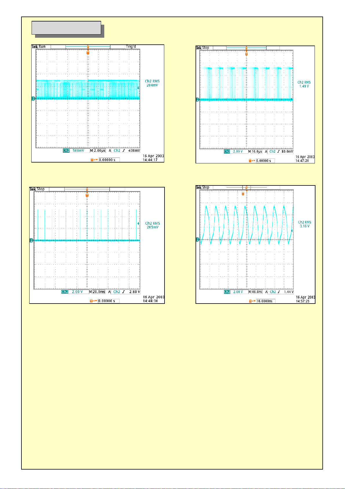
Signal-RED unput(CN#1) 2. H-SYNCO (CN#13)
V-SINKO(CN1 #14) 4. XTAL1 (U5 #9)
$

5. XTL2 (U5 #10) 6. RESET (U5 #5)
7. HFS (U4 #32) 8. HCLK( (U4 #34)
9. HDATA (U4 #33) 10. PB.5/SCL2 (U5 #12)
$

11. RXEC+ (CON4 #10) 12. REEC- (CON4 #11)
13. RXOCT (CON4 #22) 14. RXOC -(CON4 #23)
15. RXEC+ (CON4 #18) 16. RXE3- (CON4 #19)
$

17. PB.3 (U5 #14) 18. VDD5 (U5 #7)
$


<<How to dismantle Front Cover of B70A>>
1. Put the set on the flat floor. (The module should be upper side.)
2. Unhook the right-lower side (LED Lens part) of the Front Cover.
3. Unhook the left-lower side of the Front Cover with the Rear Cover.
4. Unhook the right and left side each.
5. Unhook the right & left upper side of the Front Cover and separate it from the
Rear Cover completely.
* Caution : The crack may occur if you try to separate by force.
It should be unhooked the lower side to the upper side in order.
<<How to dismantle Front Cover of B90A>>
1. Put the set on the flat floor.? (The module be upper side.)
2. Unhook the upper side each of the Front Cover.
3. Unhook the right and left side each.
4. Unhook the lower side each of the Front Cover and separate it from the Rear
Cover completely.
* Caution : The crack may occur if you try to separate by force.
It should be unhooked the upper side to the lower side in order.
 Loading...