

HYDIS HV150UX2-100 Specification

Global LCD Panel Exchange Center
THIS SPECIFICATION IS THE PROPERTY OF HYDIS AND SHALL NOT
BE REPRODUCED OR COPIED WITHOUT THE WRITTEN PERMISSION OF
HYDIS AND MUST BE RETURNED TO HYDIS UPON ITS REQUEST
TITLE : HV150UX2-100
Product Specification for Customer
www.panelook.com
PROPRIETARY NOTE
HYDIS Technologies
SPEC. NUMBER
S864-1435
B2005-C001-A (1/3)
One step solution for LCD / PDP / OLED panel application: Datasheet, inventory and accessory!
PRODUCT GROUP
TFT LCD
REV.
A
ISSUE DATE
2011.08.17
PAGE
1
OF 31
A4(210 X 297) A4(210 X 297)
www.panelook.com
Global LCD Panel Exchange Center
REVISION HISTORY
www.panelook.com
PRODUCT GROUP
TFT LCD PRODUCT A 2011.08.17
REV ISSUE DATE
REV. ECN NO. DESCRIPTION OF CHANGES DATE PREPARED
0 Internal release 2011.03.22 C.Shin
A E1108-F004 Outline drawing Change
( Rear View / Label Point Change)
2011.08.17 S.T.Ko
SPEC. NUMBER
S864-1435
B2005-C001-A (2/3) A4(210 X 297)
One step solution for LCD / PDP / OLED panel application: Datasheet, inventory and accessory!
SPEC TITLE
HV150UX2-100 Product Specification for Customer
PAGE
2
OF 31
www.panelook.com
Global LCD Panel Exchange Center
Content
6.0
Signal Timing Specification
16
11.0
Reliability Test
21
www.panelook.com
PRODUCT GROUP
TFT LCD PRODUCT
REV ISSUE DATE
h YWXXUW_UX^
s
No Item Page
1.0 General Description 4
2.0 Absolute Maximum ratings 6
3.0 Electrical specifications. 7
4.0 Optical specifications. 8
5.0 Interface Connection 12
7.0 Signal Timing waveforms 16
8.0 Input Signals, Display Colors & Gray Scale of Colors 18
9.0 Power Sequence 19
10.0 Mechanical Characteristics 20
12.0 Handling & Cautions. 22
13.0 Label 23
14.0 Packing information 25
15.0 EDID data table 27
Appendix Outline drawing (Front and Rear) 30
SPEC. NUMBER
S864-1435
B2005-C001-A (2/3)
One step solution for LCD / PDP / OLED panel application: Datasheet, inventory and accessory!
SPEC TITLE
HV150UX2-100 Product Specification for Customer
PAGE
3
OF 31
A4(210 X 297)
www.panelook.com
Global LCD Panel Exchange Center
r
N
Back Light (SMD LED Array)
VDIM
N
z
2 Channel LVDS Interface
www.panelook.com
PRODUCT GROUP
TFT LCD PRODUCT
REV ISSUE DATE
h YWXXUW_UX^
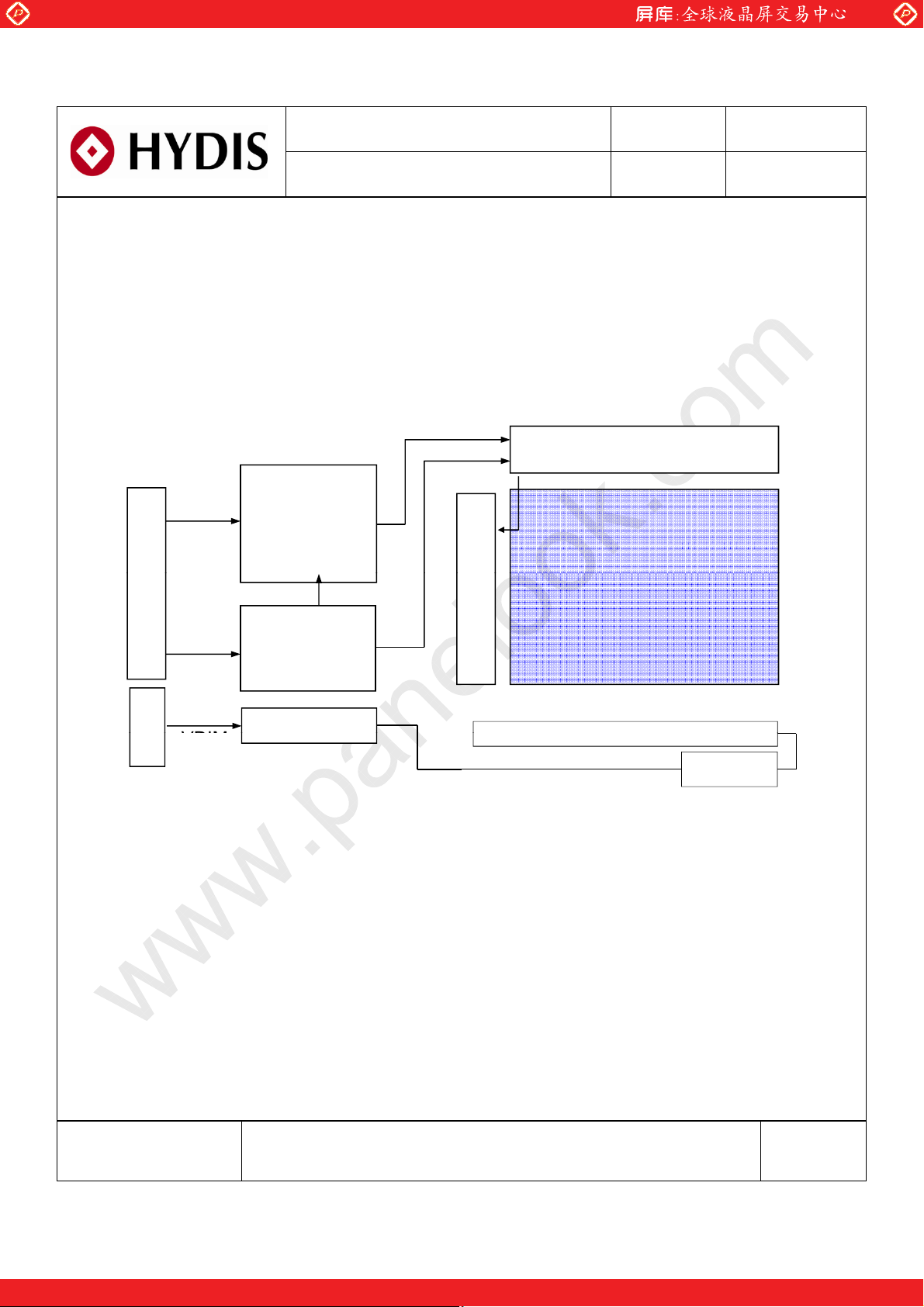
1.0 GENERAL DESCRIPTION
1.1 Introduction
HV150UX2-100 is a color active matrix TFT LCD module using amorphous silicon TFT's
(Thin Film Transistors) as an active switching devices. This module has a 15.0 inch
diagonally measured active area with UXGA resolutions (1600 horizontal by 1200 vertical
pixel array). Each pixel is divided into RED, GREEN, BLUE dots which are arranged in
vertical stripe and this module can display 262,144 colors.
This module applied LED backlight and a driving circuit on PCB assembly inside LCD panel.
Source Driver
TFT LCD Panel
1600 ശ1200
CN
1
LVDS
Input
Signal
LVDS Rx
+
T/CON
Gat
e Driver
DC/DC
Gamma
Vcom
LED Drive
C
2
VDD
HVDD
1.2 Features
z Thin and light weight
z Anti-Glare polarizer product
z Wide Temp Liquid Crystal
z LED Side mounting Backlight
z 262,144 colors
z Data enable signal mode
z Side Mounting Frame
z Green Product (RoHS)
z On Board EDID chip
CN3
SPEC. NUMBER
S864-1435
SPEC TITLE
HV150UX2-100 Product Specification for Customer
B2005-C001-A (2/3)
One step solution for LCD / PDP / OLED panel application: Datasheet, inventory and accessory!
PAGE
4
OF 31
A4(210 X 297)
www.panelook.com
Global LCD Panel Exchange Center
)
gg p
()
ensional out
e
esoaout e
317.3r
0.5(H)
243.0r
0.5(V)
7.0(D:max
)
Power consumption
PD: 1.65
W
www.panelook.com
PRODUCT GROUP
TFT LCD PRODUCT
REV ISSUE DATE
h YWXXUW_UX^
1.3 General Specification
The followings are general specifications at the model HV150UX2-100. (listed in Table 1.
<Table 1. General Specifications>
Parameter Specification Unit Remarks
Active area
Number of pixels
Pixel pitch
304.8 (H) ശ228.6 (V) (15.0” diagonal)
1600(H) ശ1200(V)
0.1905(H) ശ0.1905(V)
mm
pixels
mm
Pixel arrangement RGB Vertical stripe
Display colors 262,144 colors
Display mode Normally Black
Dim
lin
ശ
ശ
mm
Weight 510 g (typ.) g
Surface treatment AG(H40%)/2H
Back-light Bottom edge side, LED(54ea) Backlight
LED Driving Block Included in LCD, PWM dimming control
PBL: 3.46 W
P
: 5.11 W
total
SPEC. NUMBER
S864-1435
SPEC TITLE
HV150UX2-100 Product Specification for Customer
B2005-C001-A (2/3)
One step solution for LCD / PDP / OLED panel application: Datasheet, inventory and accessory!
PAGE
5
OF 31
A4(210 X 297)
www.panelook.com
Global LCD Panel Exchange Center
Logic Supply Voltage
V
3
VDD+0.3
V
Maximum wet
bulb temperature at 39
less. (Ta > 40
condensation
(40,
)
(
)
(
)
60
(
ఁ
)
www.panelook.com
PRODUCT GROUP
TFT LCD PRODUCT
REV ISSUE DATE
h YWXXUW_UX^
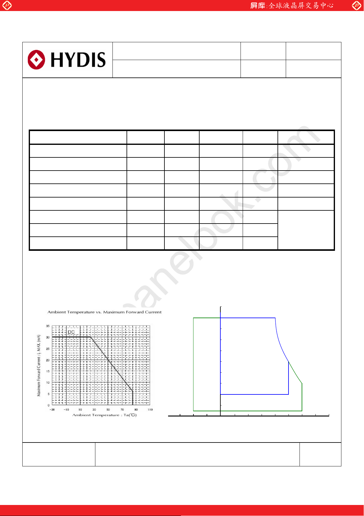
2.0 ABSOLUTE MAXIMUM RATINGS
The followings are maximum values which, if exceed, may cause faulty operation or
damage to the unit.
< Table 2. Absolute Maximum Ratings>
Parameter Symbol Min. Max. Unit Remarks
Power Supply Voltage V
LED Power Supply Voltage HV
B/L LED Current I
LED
B/L LED Reverse Voltage V
Operating Temperature T
DD
IN
DD
R
OP
-0.3 4.0 V
-0.
028V
30 mA Note 1
5V
0+50
{dY\RVTY¶j
Note 1,2
LC Operating Temperature T
Storage Temperature T
LC
SP
-40 103
-20 +60
Note 1. Ambient temperature vs. allowable forward current are shown in the figure below.
Note 2. Temperature and relative humidity range are shown in the figure below.
90 % RH Max. ( 40
O
C Ta)
-
O
C or
100
90
80
Operating Range
40
20
O
C) No
90
50, 50
60, 27
Storage Range
5
-40 -20 0 20 40 60 80
Temperature
.
SPEC. NUMBER
S864-1435
SPEC TITLE
HV150UX2-100 Product Specification for Customer
B2005-C001-A (2/3)
One step solution for LCD / PDP / OLED panel application: Datasheet, inventory and accessory!
PAGE
6
OF 31
A4(210 X 297)
www.panelook.com
Global LCD Panel Exchange Center
3.1Electrical Specifications
Back
light Power Supply Voltage
HVDD7.0
12.0
20VNote 2
Back
light LED Voltage /
V
LED
3.2
3.5
V
Note 4
P
11
6.12
W
N
4
3. Reference value, which is measured with LED Driver for 12V
www.panelook.com
PRODUCT GROUP
REV ISSUE DATE
TFT LCD PRODUCT
3.0 ELECTRICAL SPECIFICATIONS
< Table 3. Electrical specifications >
Parameter Min. Typ. Max. Unit Remarks
Logic Power Supply Voltage V
Logic Power Supply Current I
DD
DD
-
Back-light Power Supply Current I
Back-light Power Consumption P
HVDD
BL
LED Driver’s Efficiency - 82 - %
Back ight PWM Frequency F
Back light PWM Duty Ratio D
High Level PWM Signal Voltage V
Low Level PWM Signal Voltage V
High Level Differential Input Signal
Voltage
Low Level Differential Input Signal
Voltage
PWM
PWM
PWMH
PWML
V
IH
V
IL
3.0 3.3 3.6 V Note 1
- 500 650 mA Note 1
- 351 mA
- 4.215 W
200 320 350
10 100 %
2.1 3.3 5.0 V
-00.6V
- - +100 mV
-100 - - mV
h YWXXUW_UX^
Note 2,3
Note 2,3
Note 2,3
= 1.2V
V
CM
-
Back-light LED Total Voltage
Back-light LED Current /
Back-light LED Total Current
Life Time
Power Consumption
/V
P
I
/I
P
BL
LED
BL
D
LED
total
-
-
20,000
/ 28.8
20.0
/ 120
/ 31.5
21.0
/122
mA Note 4
--Hrs
- 1.65 2.15 W Note 1
- 3.46 3.97 W Note 4
-5.
ote 1,
Notes : 1. The supply voltage is measured and specified at the interface connector of LCM.
The current draw and power consumption specified is for 3.3V at 25.
a) Typ : Window XP pattern, b) Max : Vertical Sub line pattern
2. The power supply voltage and current is measured and specified at the interface
connector of LCM including LED Driver.
.
4. Reference value, which is measured without LED Driver.
5. Calculated value for reference (V
SPEC. NUMBER
S864-1435
SPEC TITLE
HV150UX2-100 Product Specification for Customer
LED
ശ I
Ý # of LEDs (54EA) ).
LED
PAGE
7
OF 31
B2005-C001-A (2/3)
One step solution for LCD / PDP / OLED panel application: Datasheet, inventory and accessory!
A4(210 X 297)
www.panelook.com
Global LCD Panel Exchange Center
The test of Optical
ificati
1
the Display surface shall stay fixed. The backlight should be operating for 30 minutes prior to
Viewing Angle
98085Deg
IBL
1W
Whit
Ry0.310
0.350
0.390
www.panelook.com
PRODUCT GROUP
TFT LCD PRODUCT
REV ISSUE DATE
h YWXXUW_UX^
4.0 OPTICAL SPECIFICATION
4.1 Overview
spec
lux and temperature = 25r2) with the equipment of Luminance meter system (Goniometer
system and TOPCONE BM-5) and test unit shall be located at an approximate distance
50cm from the LCD surface at a viewing angle of and equal to 0q. We refer to Ø=0
(=3 ) as the 3 o’clock direction (the “right”), Ø=90 (= 12 ) as the 12 o’clock direction
(“upward”), Ø=180 (= 9 ) as the 9 o’clock direction (“left”) and Ø=270(= 6 ) as the 6
o’clock direction (“bottom”). While scanning and/or Ø, the center of the measuring spot on
measurement... VDD shall be 3.3+/- 0.3V at 25qC. Optimum viewing angle direction is 6
’clock.
4.2 Optical Specifications
Parameter Symbol Condition Min. Typ. Max. Unit Remark
Horizontal
range
Vertical
Luminance Contrast ratio CR
Center
Luminance of
1 Point Y
White
e
5 Points Y5 75 85 -
Luminance
uniformity
13 points Y13 60 65 -
White Chromaticity
Red
ons shall be measured in a dark room (ambient luminance d
<Table 4. Optical Specifications>
3
CR > 10 Note 1
12
6
= 0q
w
80 85 - Deg.
-
.
80 85 - Deg.
80 85 - Deg.
500 600 - Note 2
170 200 - cd/m
2
= 0q
= 5.
%
W
W
R
x
y
x
0.273 0.313 0.353
0.289 0.329 0.369
0.555 0.595 0.635
= 0q
Reproduction
of color
Green
Blue
Response Time T
G
x
G
y
B
x
B
y
r +Td
Ta= 25 q C
= 0q
0.304 0.344 0.384
0.539 0.579 0.619
0.115 0.155 0.195
0.085 0.125 0.165
-45-ms
Color Reproduction - - - 45 - %
Cross Talk CT
SPEC. NUMBER
S864-1435
SPEC TITLE
HV150UX2-100 Product Specification for Customer
= 0q
B2005-C001-A (2/3)
One step solution for LCD / PDP / OLED panel application: Datasheet, inventory and accessory!
--2.0%
A4(210 X 297)
www.panelook.com
Note 3
PAGE
8
OF 31

Global LCD Panel Exchange Center
gg
www.panelook.com
PRODUCT GROUP
TFT LCD PRODUCT
REV ISSUE DATE
h YWXXUW_UX^
Notes : 1. Viewing angle is the angle at which the contrast ratio is greater than 10. The
viewing angles are determined for the horizontal or 3, 9 o’clock direction and the
vertical or 6, 12 o’clock direction with respect to the optical axis which is normal
to the LCD surface (see FIGURE1 as below).
2. Contrast measurements shall be made at viewing angle of = 0 and at the center
of the LCD surface. Luminance shall be measured with all pixels in the view field
set first to white, then to the dark (black) state .
Luminance Contrast Ratio (CR) is defined mathematically as CR = Luminance when
displaying a white raster / Luminance when displaying a black raster.
3. The color chromaticity coordinates specified in Table 4. shall be calculated from
the spectral data measured with all pixels first in red, green, blue, and white.
Measurements shall be made at the center of the panel.
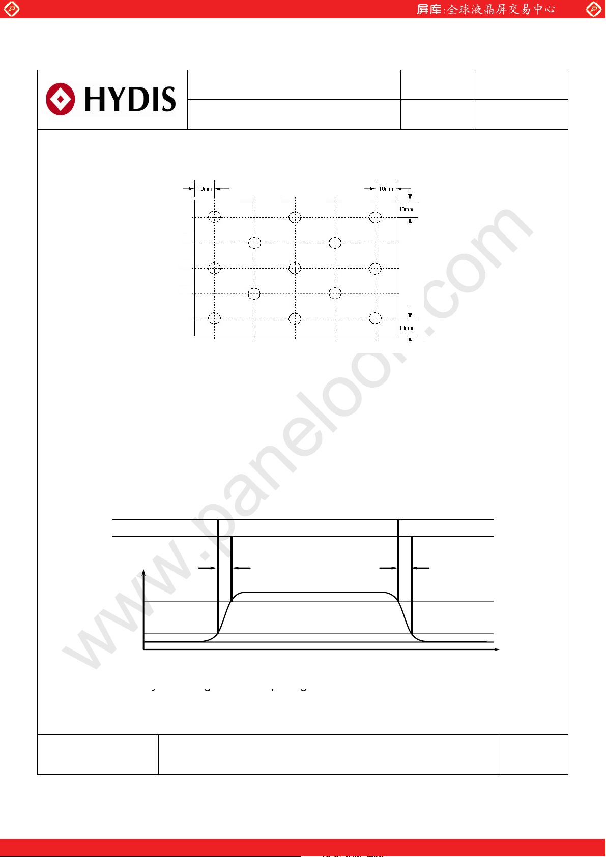
4.3 Optical measurements
Photo detector
( TOPCON BM-5A)
TFT-LCD module
Optical characteristics measurement setup
Figure 1. Measurement Set Up
Field = 2
o
50 cm
LCD panel
Center of the screen
SPEC. NUMBER
S864-1435
SPEC TITLE
HV150UX2-100 Product Specification for Customer
B2005-C001-A (2/3)
One step solution for LCD / PDP / OLED panel application: Datasheet, inventory and accessory!
PAGE
9
OF 31
A4(210 X 297)
www.panelook.com
Global LCD Panel Exchange Center
600
ith all pixels in th
y
yg pg
www.panelook.com
PRODUCT GROUP
TFT LCD PRODUCT
REV ISSUE DATE
h YWXXUW_UX^
Figure 2. White Luminance (Center) and Uniformity Measurement Locations
(5 and 13points)
400 800 1200
300
900
White luminance : Center Luminance of white is defined as luminance values of
center 1 point. Luminance shall be measured w
e view field set first
to white. This measurement shall be taken at the locations shown in FIGURE 2.
Uniformity of 5 points and 13 points : The White luminance uniformity on LCD
surface is expressed as : Y5 = Minimum Luminance of five points / Maximum
Luminance of five points (see FIGURE 2) , Y13 = Minimum Luminance of 13
points / Maximum Luminance of 13 points (see FIGURE 2.)
Figure 3. Response Time Testing
TFT Off(Black) TFT On(White) TFT Off(Black)
Tr
100%
90%
10%
0%
Td
The electro-optical response time measurements shall be made as shown in
FIGURE 3 b
switching the data input signal ON and OFF. The times needed for
the luminance to change from 10% to 90% is Tr and 90% to 10% is Td.
SPEC. NUMBER
S864-1435
SPEC TITLE
HV150UX2-100 Product Specification for Customer
B2005-C001-A (2/3)
One step solution for LCD / PDP / OLED panel application: Datasheet, inventory and accessory!
PAGE
10
OF 31
A4(210 X 297)
www.panelook.com
 Loading...