

Page 1

HUAWEI MG323 GSM M2M Module
Hardware Guide
Issue 06
Date 2013-06-13
Page 2

Huawei Technologies C o., Ltd. provides customers with com prehensive technical support and service. F or
any assistance, please contact our local office or company headquarters.
Huawei Technologies Co., Ltd.
Huawei Industrial Base, Bantian, Longgang, Shenzhen 518129, People’s Republic of China
Tel: +86-755-28780808 Global Hotline: +86-755-28560808 Website: www.huawei.com
E-mail: mobile@huawei.com
Please refer color and s ha p e to pr o duc t. Hu a wei r eser v es t he rig ht to make changes or improvements to any
of the products without prior notice.
Copyright © Huawei Technologies Co., Ltd. 2013. A ll right s reserved.
No part of this docum ent ma y be repr od uc ed or tr a ns mitted in any form or b y any means witho ut pr ior wr itte n
consent of Huawei Technologies Co., Ltd.
The product described in this manual may include copyrighted software of Huawei Technologies Co., Ltd and
possible licensors . Cus tomers shall not in any manner reproduc e, d is trib ute, modify, decompile, disassemble,
decrypt, extract, rever se engineer, lease, assign, or sublicense th e said software, unless such restrictions
are prohibited by applicable laws or such actions are approved by respective copyright holders under
licenses.
Trademarks and Permissions
, , and
Other trademarks, product, service and company names mentioned are the property of their respective
owners.
are trademarks or registered trademarks of Huawei Technologies Co., Ltd.
Notice
Some features of the pr oduct and its acces sories described h erein rely on the s oftware install ed, capacities
and settings of local network, and may not be activated or may be limited by local network operators or
network service prov iders, thus the d escriptions herein m ay not ex actly m atch the pr oduct or its access ories
you purchase.
Huawei Technologies Co., Ltd reserves the right to change or modify any information or specifications
contained in this manual without prior notice or obligation.
NO WARRANTY
THE CONTEN TS OF T HIS MANUAL ARE PRO VIDED “ AS IS”. EXCEPT AS REQUIR ED BY APPLICA BLE
LAWS, NO WARRANTIES OF ANY KIND, EITHER EXPRESS OR IMPLIED, INCLUDING BUT NOT
LIMITED TO, THE IMPLIED WARRANTIES OF MERCHANTABILITY AND FITNESS FOR A PARTICULAR
PURPOSE, ARE MADE IN RELATION TO THE ACCURACY, RELIABILITY OR CONTENTS OF THIS
MANUAL.
TO THE MAXIMUM EXTENT PERMITTED BY APPLICABLE LAW, IN NO CASE SHALL HUAWEI
TECHNOLOGIES CO., LTD BE LIABLE FOR ANY SPECIAL, INCIDENTAL, INDIRECT, OR
CONSEQUENTIAL DAMAGES, OR LOST PROFITS, BUSINESS, REVENUE, DATA, GOODWILL OR
ANTICIPATED SA VIN GS.
Import and Export Regulations
Customers shall comply with all applicable export or import laws and regulations and will obtain all necessary
governmental permits and licenses in order to export, re-export or import the product mentioned in this
manual including the software and technical data therein.
Page 3
HUAWEI MG323 GSM M2M Module
Hardware Guide
About This Document
Copyright © Huawei Technologies Co., Ltd.
History
About This Document
Version Date Chapter Descriptions
01 Creation
02 2010-10-25 1 Deleted “1.2 Related Documents”
3.1 Deleted “Charging Inter face (TBD)”
03
3.6.1 Revised “Table 3-5 UA RT 1 int er f ace signals”
3.8
7
2011-07-18 2.2
3.5.2 Added the maximum time of TERM_ON
3.6
5.2
5.4
5.5.2
Deleted “Charging Inter face (TBD)”
Added “Audio Interface”
Revised “Figure 7-1 Circuits of typical
interfaces in the MG323 mo dule”
Added authentication information-CCC, GCF
and mode of audio services
Added signal of the RING w hil e receiving a
message and a voice call
Revised “Table 5-1 Extreme working
conditions for the MG323 module”
Revised “Table 5-3 Sequence numbers of
pins and definitions o f signals on the B2B
interface” and “Table 5-4 Electrical features
of application interfaces”
Revised “Table 5-6 Working current of the
MG323 module”
04 2011-08-22 3.2
Issue 06 (2013-06-13)
6.3
6.4 Revised “Figure 6-5 Structure fixing hole”
Huawei Proprietary and Confidential
Specified the mode of the 50-pin B2B
connector
Revised “Figure 3-1 Sequence and
definitions of pins on the B2 B signal
interface”
3
Page 4
HUAWEI MG323 GSM M2M Module
Hardware Guide
About This Document
Copyright © Huawei Technologies Co., Ltd.
Version Date Chapter Descriptions
05 2013-03-22 2.2 Updated Table 2-1 Feature
2.3
Updated Figure 2-1 App lic at ion block
diagram of the MG323 modul e
2.4
Updated Figure 2-2 Circ ui t block diagram of
the MG323 module
3.2
Updated Table 3-1 Definiti ons of pins on the
BEB connector
3.3.2 Updated VBAT interface
3.3.3 Updated Figure 3-3 VCO IN interface circuit
3.4.3 Updated Figure 3-5 Power-off time sequence
3.5.2
Updated Figure 3-6 Connections of the
TERM_ON and RESET pins
3.5.3 Updated Figure 3-7 Driv in g circ u it
3.6.2
Added the description for the level of UART
interface
3.8.3
Updated Figure 3-13 External circuit for 32 Ω
handsets/16 Ω headsets
3.8.3
Updated Figure 3-14 External circuit for the
microphone interface
5.2
Updated extreme working conditions of
MG323 module
5.4
Updated Table 5-4 Elect rical featur es of
application interfaces
5.2.2 Updated working current of MG323 module
6.4
Updated Figure 6-6 MG323 module
installation
7
Updated Figure 7-1 Circuits of typical
interfaces in the MG323 mo dule
06 2013-06-13 3.2 Updated Table 3-1
3.4.2 Updated Figure 3-4 Power-on time sequence
3.6.1 Updated Chapter 3.6.1 Overview
3.7.3
Deleted Chapter 3.7.3 ESD Protection for the
SIM Card Interface
Issue 06 (2013-06-13)
Huawei Proprietary and Confidential
4
Page 5
HUAWEI MG323 GSM M2M Module
Hardware Guide
About This Document
Copyright © Huawei Technologies Co., Ltd.
Version Date Chapter Descriptions
3.8 Updated Chapter 3.8 Audi o Interface
4.6
7
Updated Table 4-3 Recommended
specifications of the antenna interface
Updated Figure 7-1 Circuits of typical
interfaces in the MG323 mo dule
Issue 06 (2013-06-13)
Huawei Proprietary and Confidential
5
Page 6

HUAWEI MG323 GSM M2M Module
Hardware Guide
Contents
Copyright © Huawei Technologies Co., Ltd.
Contents
1 Introduction.................................................................................................................................... 8
1.1 Overview .......................................................................................................................................... 8
2 Overall Description ...................................................................................................................... 9
2.1 About This Chapter ........................................................................................................................... 9
2.2 Function Overview............................................................................................................................ 9
2.3 Application Block Diagram .............................................................................................................. 11
2.4 Circuit Block Diagram ...................................................................................................................... 11
3 Description of the Application Interfaces .............................................................................. 13
3.1 About This Chapter ......................................................................................................................... 13
3.2 B2B Connector Interface ................................................................................................................ 13
3.3 Power Interface .............................................................................................................................. 16
3.3.1 Overview ................................................................................................................................ 16
3.3.2 VBAT Interface ....................................................................................................................... 17
3.3.3 VCOIN Interface .................................................................................................................... 18
3.3.4 VIO Interface ......................................................................................................................... 18
3.4 Power-On and Power-Off Time Sequence ..................................................................................... 18
3.4.1 Overview ................................................................................................................................ 18
3.4.2 Power-On Time Sequence .................................................................................................... 19
3.4.3 Power-Off Time Sequence .................................................................................................... 20
3.4.4 RESET ................................................................................................................................... 20
3.5 Signal Control Interface .................................................................................................................. 20
3.5.1 Overview ................................................................................................................................ 20
3.5.2 Input Signal Control Pins ....................................................................................................... 21
3.5.3 Output Signal Control Pin ...................................................................................................... 22
3.6 UART Interface ............................................................................................................................... 23
3.6.1 Overview ................................................................................................................................ 23
3.6.2 Circuit Recommended for the UART Interface ...................................................................... 24
3.7 SIM Card Interface ......................................................................................................................... 25
3.7.1 Overview ................................................................................................................................ 25
3.7.2 Circuit Recommended for the SIM Card Interface ................................................................ 26
3.8 Audio Interface ............................................................................................................................... 27
4 Antenna Interface ........................................................................................................................ 29
Issue 06 (2013-06-13)
Huawei Proprietary and Confidential
6
Page 7

HUAWEI MG323 GSM M2M Module
Hardware Guide
Contents
Copyright © Huawei Technologies Co., Ltd.
4.1 About This Chapter ......................................................................................................................... 29
4.2 Antenna Installation ........................................................................................................................ 29
4.3 Coaxial Cable and RF Connector .................................................................................................. 30
4.4 ESD Protection for the Antenna Interface ...................................................................................... 32
4.5 RF Specifications of the Antenna Interface .................................................................................... 32
4.6 Specifications of the Antenna Interface .......................................................................................... 34
5 Electrical and Reliability Features ........................................................................................... 35
5.1 About This Chapter ......................................................................................................................... 35
5.2 Extreme Working Conditions .......................................................................................................... 35
5.3 Operating and Storage Temperatures and Humidity ...................................................................... 36
5.4 Electrical Criteria of Application Interfaces ..................................................................................... 36
5.5 Power Supply Features .................................................................................................................. 40
5.5.1 Input Power Supply ............................................................................................................... 40
5.5.2 Working Current .................................................................................................................... 40
5.6 Reliability Features ......................................................................................................................... 42
5.7 ESD Features ................................................................................................................................. 44
6 Mechanical Specifications ......................................................................................................... 45
6.1 Overview ........................................................................................................................................ 45
6.2 Dimensions ..................................................................................................................................... 45
6.3 Dimensions of the B2B Connector ................................................................................................. 46
6.4 MG323 Module Installation Desc r ipt ion ......................................................................................... 48
6.5 Specification Selection for Fasteners ............................................................................................. 50
7 Appendix A Circuits of Typical Interfaces ............................................................................ 52
8 Appendix B Acronyms and Abbreviations ............................................................................ 53
Issue 06 (2013-06-13)
Huawei Proprietary and Confidential
7
Page 8

HUAWEI MG323 GSM M2M Module
Hardware Guide
Introduction
Copyright © Huawei Technologies Co., Ltd.
1.1 Overview
This document describes the hardware application interfaces and air interfaces that
are provided when the Hu aw ei MG 323 GSM M2M module (hereinafter referred to as
the MG323 module) is used.
1 Introduction
This document helps you to understand the interface specifications, electrical
features, and related product information of the MG323 module.
Issue 06 (2013-06-13)
Huawei Proprietary and Confidential
8
Page 9
HUAWEI MG323 GSM M2M Module
Hardware Guide
Overall Description
Copyright © Huawei Technologies Co., Ltd.
2.1 About This Chapter
This chapter gives a gener al description of the MG323 module and provides:
Function Overview
Application Block Diagram
Circuit Blo ck Diagram
2 Overall Description
2.2 Function Overview
Table 2-1 Feature
Feature Description
Working bands
Maximum
transmission
power
Receiver
sensitivity
Operating
Temperature
Ambient
temperature for
storage
Four supported frequenc y bands: GSM850 MHz/900 MHz/1800
MHz/1900 MHz
GSM850 Class 4 (2 W)
EGSM900 Class 4 (2 W)
DCS1800 Class 1 (1 W)
PCS1900 Class 1 (1 W)
< –107 dBm
Normal operating temperature: –20°C to +70°C
Extended operating te mp er at ur e
–40°C to +85°C
[1]
: –30°C to +75°C
Power voltage 3.3 V to 4.8 V (3.8 V is recommended. )
Issue 06 (2013-06-13)
Huawei Proprietary and Confidential
9
Page 10
HUAWEI MG323 GSM M2M Module
Hardware Guide
Overall Description
Copyright © Huawei Technologies Co., Ltd.
Feature Description
Power
Power-off current: 50 µA
consumption
(current)
Average
DRX=2 < 3.0 mA
standby current
DRX=5 < 2.5 mA
DRX=9 < 2.0 mA
GPRS Class 10 (maximum): 455 mA
Protocols GSM/GPRS Phase2/2+
AT commands
See the HUAWEI MG323 Seri es Wireless Module AT Command
Interface Specification.
Application
UART1 (supporting 8-wire UART)
interface (50pin B2B
connector)
One standard Subscriber Identity Module (SIM) card interface
(Class B or Class C)
Interfaces for two analog audio channels
Power Interface
Network status light-emitting diode (LED) control inter face
Antenna
Hirose U.FL-R-SMT-1(80) 50 Ω antenna connector
interface
Antenna pad
Voice services Two analog voice channels
SMS
New message alert, text message receiving, an d text message
sending
Management of text messages: read messages, delete
messages, storage status, and m essage list
Support for the protocol data unit (PDU) mode
GPRS GPRS CL AS S 10
Encoding schemes: CS 1, CS 2, CS 3, and CS 4
Maximum downlink trans m ission rate: 85.6 kbps
Maximum uplink transm ission rate: 42.8 kbps
Packet Broadcast Control Channel (PBCCH)
Embedded with TCP/IP pr ot ocols, supporting multipl e link s
Circuit
CSD data services at the maximum rate of 9.6 kbit/s
Switched Data
(CSD) data
services
Physical
features
Dimensions (L × W × H): 35 mm × 32.5 mm × 3.05 mm
Weight: 5.8 g
Issue 06 (2013-06-13)
Huawei Proprietary and Confidential
10
Page 11
HUAWEI MG323 GSM M2M Module
Hardware Guide
Overall Description
Copyright © Huawei Technologies Co., Ltd.
Feature Description
Certification
information
Restriction of the use of cer t ain Hazardous Substances (RoHS),
European Conformity (CE), Federal Communications
Commission (FCC), CMIIT, China Compulsory Certification
(CCC), GCF (GSM Certification Forum)
.
[1]:The temperatures outside of the range –20°C to +70°C; the module might slightly deviate
from 3GPP TS 45.005 specifications.
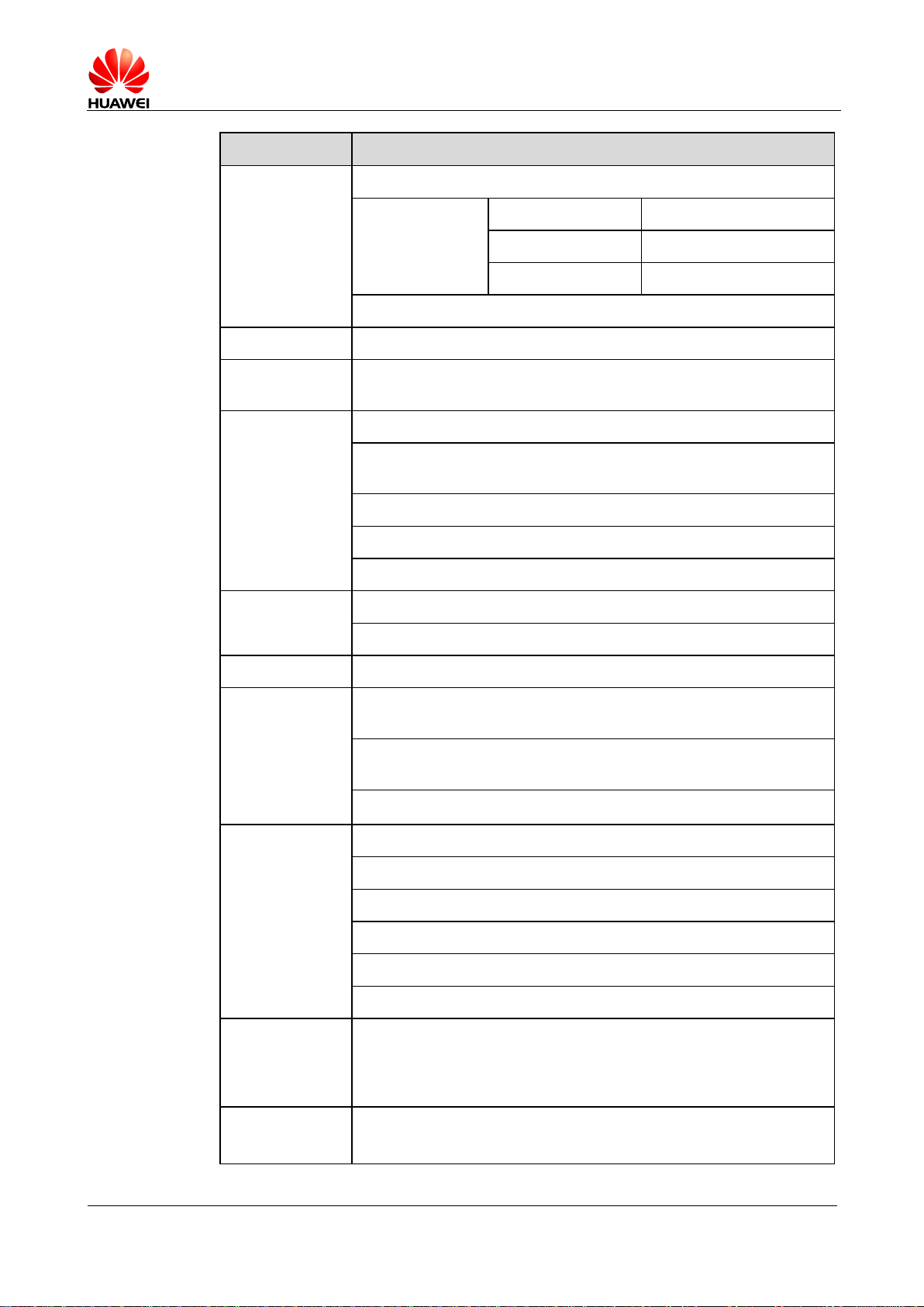
2.3 Application Block Diagram
Figure 2-1 shows the application bloc k d ia gr am of the MG323 module.
Figure 2-1 Application block diagram of the MG323 module
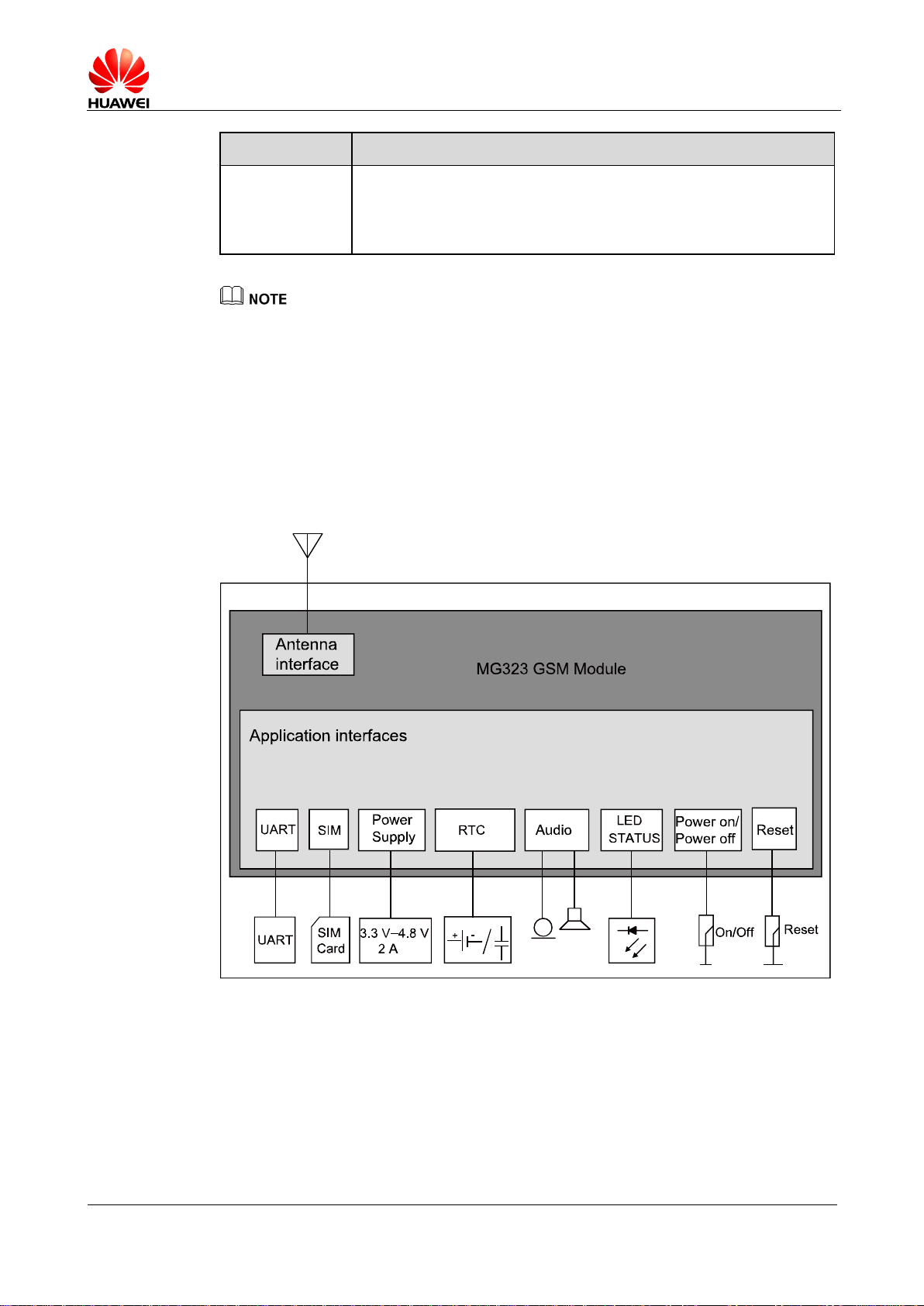
2.4 Circuit Block Diagram
The circuit block diagram and major functional units of the MG323 module con tain
the following part s:
Baseband controller
Issue 06 (2013-06-13)
Huawei Proprietary and Confidential
11
Page 12
HUAWEI MG323 GSM M2M Module
Hardware Guide
Overall Description
Copyright © Huawei Technologies Co., Ltd.
Power management
Multi-chip package (MCP) memory
Radio frequency (RF) tr ansceiver
26 MHz clock
32 kHz clock
RF front-end modules
Receive filter
Figure 2-2 Circuit block diagram of the MG323 module
Issue 06 (2013-06-13)
Huawei Proprietary and Confidential
12
Page 13
HUAWEI MG323 GSM M2M Module
Hardware Guide
Description of the Application Interfaces
Copyright © Huawei Technologies Co., Ltd.
1 2
49 50
3 Description of the Application Interfaces
3.1 About This Chapter
This chapter mainly descr ibes the external applicat io n int er f aces of the MG323
module, including:
B2B Connector Interface
Power Interface
Power-On and Power-Of f T ime Sequence
Signal Control Interface
UART Interface
SIM Card Interface
Audio Interface
3.2 B2B Connector Interface
The MG323 module uses a 50-pin B2B connector as it s ext er nal interface. For det ai ls
about the model and dimensions of the B2B connector, see “ 6.3 Dimensio ns of the
B2B Connector”.
Figure 3-1 shows the sequence and definitions of pins on the 50-pin B2B sign al
interface of the MG323 m odule.
Figure 3-1 Sequence and definitions of pins on the B2B signal interface
Issue 06 (2013-06-13)
Huawei Proprietary and Confidential
13
Page 14
HUAWEI MG323 GSM M2M Module
Hardware Guide
Description of the Application Interfaces
Copyright © Huawei Technologies Co., Ltd.
Table 3-1 Definitions of pins on the B2B connector
Pin
Pin Name I/O Description DC Characteristics (V)
No.
Normal MUX Min. Tpy. Max
1 SIM_CLK - O
2 INTEAR_N - AO
3 VSIM - P
4 INTEAR_P - AO
5 SIM_DATA - I/O
6 EXTEAR_P - AO
7 SIM_RST - O
Clock signal of the SIM
card
Negative pole of the
output of h
speaker
andset
Power supply of the
SIM card
Positive pole of the
output of h
speaker
andset
Data signal of the SIM
card
Positive pole of the
output of headset
speaker
Reset signal of the SIM
card
- 1.80/2.90 -
- - -
- 1.80/2.90 -
- - -
- 1.80/2.90 -
- - -
- 1.80/2.90 -
8 EXTEAR_N - AO
9 NC - -
Negative pole of the
output of
speaker
headset
Not connected, please
- - -
- - -
keep this pin open
10 INTMIC_N - AI
Negative pole of the
input of h
microphone
andset
- - -
11 GND - - Ground - - 12 INTMIC_P - AI
13 NC - -
Positive pole of the
input of h
microphone
andset
Not connected, please
- - -
- - -
keep this pin open
14 EXTMIC_P - AI
15 NC - -
Positive pole of the
input of h
microphone
eadset
Not connected, please
- - -
- - -
keep this pin open
16 EXTMIC_N - AI
Issue 06 (2013-06-13)
Negative pole of the
input of h
microphone
Huawei Proprietary and Confidential
eadset
- - -
14
Page 15
HUAWEI MG323 GSM M2M Module
Hardware Guide
Description of the Application Interfaces
Copyright © Huawei Technologies Co., Ltd.
Pin
Pin Name I/O Description DC Characteristics (V)
No.
Normal MUX Min. Tpy. Max
17 NC - -
Not connected, please
- - -
keep this pin open
18 GND - - Ground - - 19 NC - -
Not connected, please
- - -
keep this pin open
20 TERM_ON - I
21 NC - -
Power on/power off
control
Not connected, please
-
- - -
internal
pulled up
-
keep this pin open
22 RESET - I Hardware res et –0.40 2.80 3.20
23 NC - -
Not connected, please
- - -
keep this pin open
24 UART1_DCD - O DCE data carrier detect –0.40 2.80 3.20
25 LED_STATUS - O
Network status
–0.40 2.80 3.20
indication
26 NC - -
Not connected, please
- - -
keep this pin open
27 NC - -
Not connected, please
- - -
keep this pin open
28 UART1_CTS - O DCE clear to send –0.40 2.85 3.25
29 UART1_RD - O DCE transmit data –0.40 2.85 3.25
30 NC - -
Not connected, please
- - -
keep this pin open
31 NC - -
Not connected, please
- - -
keep this pin open
32 UART1_DTR - I
DCE data terminal
–0.40 2.80 3.20
ready
33 UART1_TD - I DCE receive data –0.40 2.80 3.20
34 UART1_RTS - I DCE request to send –0.40 2.85 3.25
35 VCOIN - P
Standby power input of
2.00 3.00 3.15
the RTC
36 UART1_DSR - O DCE data set ready –0.40 2.80 3.20
37 NC - -
38 UART1_RING - O DCE ring indicator –0.40 2.80 3.20
Issue 06 (2013-06-13)
Not connected, please
- - -
keep this pin open
Huawei Proprietary and Confidential
15
Page 16
HUAWEI MG323 GSM M2M Module
Hardware Guide
Description of the Application Interfaces
Copyright © Huawei Technologies Co., Ltd.
Pin
Pin Name I/O Description DC Characteristics (V)
No.
Normal MUX Min. Tpy. Max
39 NC - -
Not connected, please
- - -
keep this pin open
40 VIO - P External power output 2.70 2.80 2.95
41 GND - - Ground - - 42 VBAT - P Power supply input 3.30 3.80 4.80
43 GND - - Ground - - 44 VBAT - P Power supply input 3.30 3.80 4.80
45 GND - - Ground - - 46 VBAT - P Power supply input 3.30 3.80 4.80
47 GND - - Ground - - 48 VBAT - P Power supply input 3.30 3.80 4.80
49 GND - - Ground - - 50 VBAT - P Power supply input 3.30 3.80 4.80
P indicates power pins; I indicates pins for digital signal input; O indicates pins for digital
signal output; AI indicates pins for analog signal input; AO indicates pins for analog signal
input.
The NC (Not Connected) pins are internally connected to the module. Therefore, these pins
should not be used, otherwis e they may cause problems. Please contact us for more
details about this information.
3.3 Power Interface
3.3.1 Overview
The power supply part of the B2B interface of the M G 323 module contains:
VBAT interface for the power supply
VCOIN interface for the standby power supply of the real-time clock (RTC)
VIO interface for external power output
Table 3-2 lists the definitions of the pins on the power supply interface.
Issue 06 (2013-06-13)
Huawei Proprietary and Confidential
16
Page 17
HUAWEI MG323 GSM M2M Module
Hardware Guide
Description of the Application Interfaces
Copyright © Huawei Technologies Co., Ltd.
Module
(DCE)
VBAT
VBAT
100 nF
10 μF
+
220μF
+
220μF
+
220μF
+
220μF
+
220μF
Table 3-2 Definitions of the pins on the power supply interface
Pin No. Signal Name I/O Description
42, 44, 46, 48, 50 VBAT P Pins for Power supply in put
41, 43, 45, 47, 49 GND - GND
35 VCOIN P
40 VIO P Pin for external power output
3.3.2 VBAT Interface
When the MG323 module works normally, power is supplied through the V BAT pins
and the voltage ranges from 3.3 V to 4.8 V (typical value: 3. 8 V) . The 50-pin B2B
connector provides fiv e VB AT pins and five GND pi ns for ext ernal power input. To
ensure that the MG323 module works normally, all the pins must be used ef f iciently.
When the MG323 module is used for different ex t er nal applications, pay special
attention to the design for t he pow er supply. When the MG323 m odule transmits
signals at the maximum p ow er, the transient current may reach the t r ansient peak
value of about 2.0 A due to the differe nces in actual network environments. In this
case, the VBAT voltage greatly drops. Make sure that t he voltage does not decrease
below 3.3 V in any case. Otherwise, exceptions such as r estart of the MG323 module
may occur.
A low-dropout (LDO) regulator or switch pow er with current output of more t han 2 A is
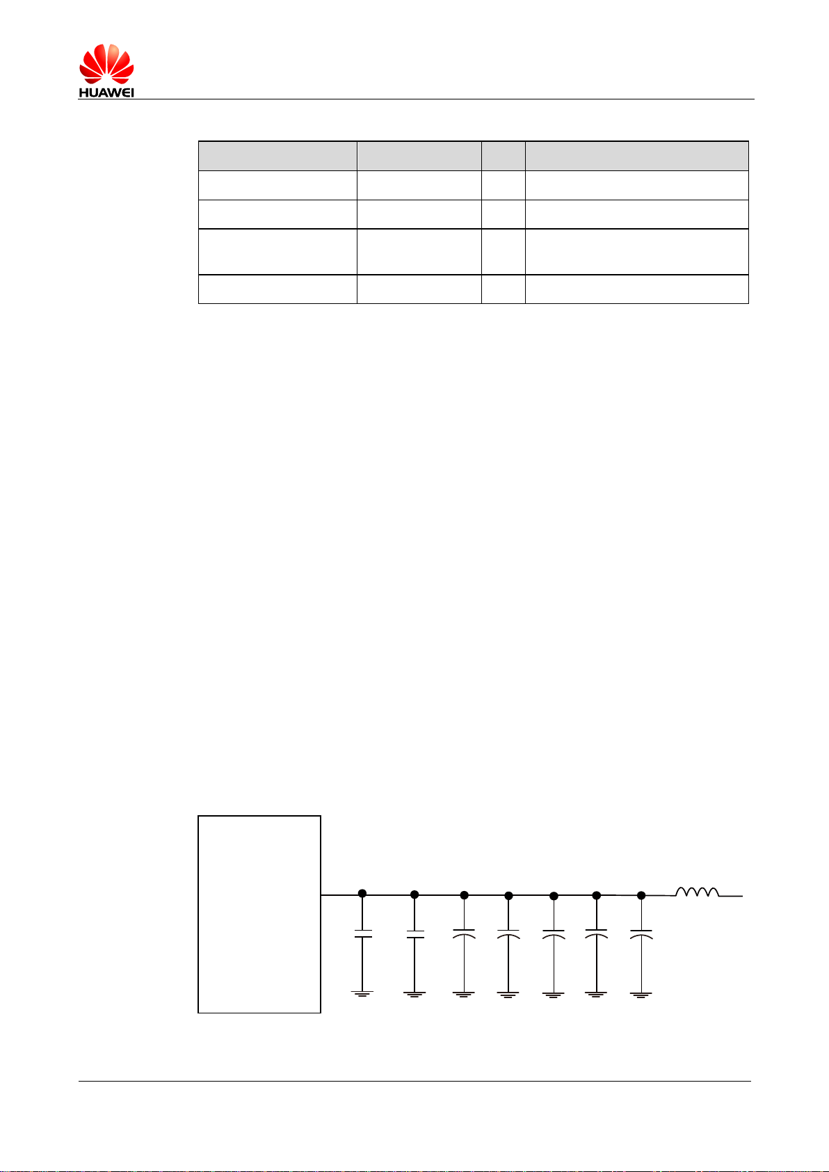
recommended for exter nal power supply. Furthermore, At least five 220 µF storage
capacitors should be connected in parallel at the power interface of the MG323
module. In addition, to reduce the im pact of channel impedance on voltage dro p, you
are recommended to try to shorten the power supply circuit of the VBAT interface.
Pin for standby power inp ut of
the RTC
It is recommended to employ a ferrite bead in series on VBAT power circuit to
improve the EMI performanc e. And the rated current of the ferrite bead is required at
least 2 A.
Figure 3-2 shows the recommended pow er circuit of MG323 module.
Figure 3-2 Recommended power circuit of MG323 module
Issue 06 (2013-06-13)
Huawei Proprietary and Confidential
17
Page 18

HUAWEI MG323 GSM M2M Module
Hardware Guide
Description of the Application Interfaces
Copyright © Huawei Technologies Co., Ltd.
3.3.3 VCOIN Interface
VCOIN is an interface for standby power input of the RTC in the MG323 module. If
the VBAT interface is ready for power supp ly, it on priority suppli es t he RTC with
power . If the VBAT interface is not ready, the VCOIN interface provides standby
power input for the RTC. In this case, the MG323 m odule needs 5 µA to maintain the
RTC function.
You can use an external battery to supply power t hr ough the VCOIN interface. The
recommended volt age is 3 V. You can also use an external capacitor if you do not
use a battery. The capacitance d et ermines the duration of the RTC when the VBAT
interface is not ready.
The MG323 module supports charging exter nal standby batteries. When the VBAT
voltage is 3.8 V, the charging current is about 0.6 mA (typical value). Figure 3-3
shows two types of circuits for your reference.
Figure 3-3 VCOIN interface circuit
3.3.4 VIO Interface
Through the VIO interface , the MG323 module can supply 2. 8 V pow er ext er nally
with an output current of 10 mA (typical value) for external level conv er sion or other
applications.
If the MG323 module is in slee p mode, the VIO interface is in the l ow power
consumption state (< 500 µA). If the MG323 module is in power down mode, the VIO
is in the disabled state. If VIO pin is not in use, disc onnect the pin and make sure it is
not grounded.
3.4 Power-On and Power-Off Time Sequence
3.4.1 Overview
The power-on, power-off, and reset control parts of the B2B i nt er face of the MG323
module includes power-on/power-off interface signal (TERM_ON) and the hardware
reset interface signal (RESET). Table 3-3 lists the definitions of the interface pins.
Issue 06 (2013-06-13)
Huawei Proprietary and Confidential
18
Page 19

HUAWEI MG323 GSM M2M Module
Hardware Guide
Description of the Application Interfaces
Copyright © Huawei Technologies Co., Ltd.
250 ms (min)
VBAT
TERM_ON
VIO
Fetch Ext
Code
6.6 ms
6.3 ms
V
io
is set
Sampling period used to
select V
gpio/Vmem
2.8 V
2.3 V
1s
130 ms
185 ms
HW
Init
Power-Key
SW Debouncing
Nominal
SW
High-Z
Table 3-3 Definitions of pins of the power-on/power-off and reset interfaces
Pin No. Signal Name I/O Description
20 TERM_ON I Pin for controlling power-on and power-off
22 RESET I Pin for resetting the hardwar e
3.4.2 Power-On Time Sequence
Make sure that the MG32 3 mo dule is powered on at the v oltage and operating
temperature in the recommended range. Otherwise, the module may get
damaged or work improper ly.
External application inter f ac es must be powered on after t he module is powered
on.
You can power on the MG323 module through the TERM_ON interface. The software
will report relevant information according to the act ual set t i ngs after the module is
powered on. For example, the AT command automatically reports ^SYSSTART[1]. In
this case, the external VI O inter face is enabled and supplies 2. 8 V pow er.
[1] For specific setting information about the power-on/power-off software, see the HUAWEI
MG323 Series Wireless Module AT Command Interface Specification.
Figure 3-4 shows the power-on time sequence.
Figure 3-4 Power-on time sequence
Issue 06 (2013-06-13)
Huawei Proprietary and Confidential
19
Page 20

HUAWEI MG323 GSM M2M Module
Hardware Guide
Description of the Application Interfaces
Copyright © Huawei Technologies Co., Ltd.
Fetch Ext Code in the figure is a file system in the MG323 module.
Before powering on the MG323, make sure that TERM_ON is in High-Z condition.
3.4.3 Power-Off Time Sequence
The MG323 module supports power-off through the TERM_ON interface or the
AT^SMSO command. Figure 3-5 shows the power-off time sequence.
Figure 3-5 Power-off time sequence
The processing of the power-off event depends on the normal stop time of the file system
in the MG323 module. The processing varies with the capacity of the file system.
Do not suddenly turn off the VBAT power when the module is working. It is recommended
to power-off the module before turning off the VBAT power.
3.4.4 RESET
The MG323 module supports hardware reset fun c t i on. If the software of the MG 323
module stops responding, you can reset the hardware through the RESET signal.
After the hardware is reset, the software starts powering on the m odule and reports
relevant information according to the actual settings. For example, the AT command
automatically report s ^SYSSTART. In this case, the external VI O int er f ace is enabled
and supplies 2.8 V power.
3.5 Signal Control Interface
3.5.1 Overview
The signal control part of the B2B interface in the MG323 module consists of:
Power-on/off (TE RM_ON) pin
Hardware reset (RESET) pin
Issue 06 (2013-06-13)
Huawei Proprietary and Confidential
20
Page 21

HUAWEI MG323 GSM M2M Module
Hardware Guide
Description of the Application Interfaces
Copyright © Huawei Technologies Co., Ltd.
Network status LED (LED_STATUS) pin
Table 3-4 lists the pins on the signal control interface .
Table 3-4 Pins on the signal control interface
Pin No. Signal Name I/O Description
20 TERM_ON I Pin for controlling power-on and power-off
22 RESET I Pin for resetting the hardware
25 LED_STATUS O Pin for network status LED
3.5.2 Input Signal Control Pins
The MG323 module implements power-on and power-off and resets the hardware
through the input signal contr ol pins.
The TERM_ON pin is used to implement power-on and power-off. If the TE RM_ON
pin is pulled down for 1 second to 2 seconds, the module is pow er ed on; if the
TERM_ON p in is pulled down for 1 secon d t o 2 seconds again, the module is
powered off.
The RESET pin is used t o reset the hardware. When the software st ops responding,
the RESET pin can be pulled down for at least 10 ms to reset the hardware.
As the RESET and TERM_ON signals are relatively sensitive, it is recommended that
you install a 10 nF capacitor near t he R ESET and T ER M _ON pins of the B2B
interface for filtering. I n addition, when you design a circuit on the PCB of the
interface board, it is reco m m ended that the circuit length not exceed 20 mm and that
the circuit be kept at a distance of 2.54 mm (100 mil) at least from the PCB edge.
Furthermore, you need t o w r ap t he ar ea adjacent to the signal wire with a gr ound
wire. Otherwise, the module may be reset due to interference.
Figure 3-6 shows the con nect ions of the TERM_O N and RESET pins.
Issue 06 (2013-06-13)
Huawei Proprietary and Confidential
21
Page 22

HUAWEI MG323 GSM M2M Module
Hardware Guide
Description of the Application Interfaces
Copyright © Huawei Technologies Co., Ltd.
Application Device
(Host)
2.2 kΩ
RESET
TERM_ON
2.2 kΩ
10 nF
10 nF
b
b
c
e
c
e
HUAWEI Module
(Modem)
Figure 3-6 Connections of the TERM_ON and RESET pins
3.5.3 Output Signal Control Pin
The MG323 module provides a network status LED pin LED_STAT US. The pulse
signal output through this pin controls the status LED on the user interface board to
display the network status.
Different blinking modes of the status L ED indicate different net w ork status. Table 3-5
describes the status of the LED_STA TUS pin.
Table 3-5 Status of the LED_STATUS pin
Working or Network Status Output Status of the LED_STATUS Pin
Sleep mode A low-level signal is output continuously.
Network-searching or non-network
status (including the cas e when the
A high-level signal is output for 0.1s in a
period of 1s.
SIM card is not inserted and t he case
when the PIN number is unblocked)
Registered with a 2G network
A high-level signal is output for 0.1s in a
period of 3s.
GPRS data service
A high-level signal is output for 0.1s in a
period of 0.125s.
Voice call
A high-level signal is output
continuously.
In practical application, t he LED_STATUS pin cannot be directly used to dr iv e the
status LED. The LED_STATUS p in needs to be used with a triode. To select a
suitable current-limiting resistor for t he LED, check the actual volt age drop and rated
Issue 06 (2013-06-13)
current of the LED. Figure 3-7 shows the driving circuit.
Huawei Proprietary and Confidential
22
Page 23

HUAWEI MG323 GSM M2M Module
Hardware Guide
Description of the Application Interfaces
Copyright © Huawei Technologies Co., Ltd.
Figure 3-7 Driving circuit
3.6 UART Interface
3.6.1 Overview
The MG323 module provides the UART1 (8-wire UART) interface for one
asynchronous communication channel. As the UART1 interface supports signal
control through standard modem handshake, AT commands are entered and serial
communication is perfor m ed t hr ough the UART1 interface. The UAR T1 has the
following features:
Full-duplex
Baud rate clock generated by the system clock
Direct me mory access (DMA) transmission
Baud rate ranging from 9600 bit/s to 230400 bit/s (115200 bit/s by default)
Self-adapted baud rate ranging from 9600 bit/s t o 115200 bit/s
Table 3-6 lists the UART1 interface signals.
Table 3-6 UART1 interface signals
Pin No. Signal Name Description Feature Direction
29 UART1_RD
Issue 06 (2013-06-13)
DCE transmit
data
The data terminal
equipment (DTE)
receives serial
data.
Huawei Proprietary and Confidential
Data circuitterminating
equipment
(DCE) to DTE
23
Page 24

HUAWEI MG323 GSM M2M Module
Hardware Guide
Description of the Application Interfaces
Copyright © Huawei Technologies Co., Ltd.
Pin No. Signal Name Description Feature Direction
33 UART1_TD
38 UART1_RING
32 UART1_DTR
34 UART1_RTS
36 UART1_DSR
28 UART1_CTS
24 UART1_DCD
DCE receive
data
DCE ring
indicator
DCE data
terminal ready
DCE request to
send
DCE data set
ready
DCE clear to
send
DCE data
carrier detect
The DTE transmits
DTE to DCE
serial data.
The DCE notifies
DCE to DTE
the DTE of a
remote call.
The DTE is ready. DTE to DCE
The DTE requests
DTE to DCE
the DCE to send
data.
The DCE is ready. DCE to DTE
The DCE has
DCE to DTE
switched to the
data receiving
mode.
A data link is set
DCE to DTE
up.
3.6.2 Circuit Recommended for the UART Interface
Figure 3-8 shows the con nect ion of the UART1 int erface in the MG323 modul e ( DC E)
with the host (DTE).
Figure 3-8 Connection of the UART1 interface in the MG323 module (DCE) with the
host (DTE)
When an MG323 module receives a n SM ( Short Message), a low-level signal i s
output through the RING ( pin 3 8) for 1s, as s hown in Figure 3-9 .
Issue 06 (2013-06-13)
Huawei Proprietary and Confidential
24
Page 25

HUAWEI MG323 GSM M2M Module
Hardware Guide
Description of the Application Interfaces
Copyright © Huawei Technologies Co., Ltd.
1s 1s 1s
4s 4s 4s
Figure 3-9 The signal through the RING after the MG323 receives an SM
When an MG323 Module receives a v oice call, a periodical low lev el si gnal for 1s and
a high level signal for 4s are out put by RING, as shown in Figure 3-10 .
Figure 3-10 The signal through the RING after the MG323 receives a voice call
For detailed application of the MG323 UART1 interface, see HUAWEI Module UART Serial
Port Design Guide.
The maximum level of UART1_DCD, UART1_RING, UART1_DSR and UART1_DTR
signals is 3.2 V, and the maximum level of UART1_TD, UART1_RD, UART1_CTS and
UART1_RTS signals is 3.25 V. Therefore, if the UART signals need to be connected the
signal with 3.3 V, a level conversion curcuit is required.
UART1 interface must be powered on after the module is powered on to avoid the wind
blow in which may cause the module cannot work properly.
The level of RS-232 Transceivers must match that of the MG323 module.
3.7 SIM Card Interface
3.7.1 Overview
The MG323 module provides a SIM card interface c om plying with the ISO 7816-3
standard and suppor ts automatic detection of a Class B SIM card or a Class C SIM
card. Table 3-7 lists the SIM card interface signals.
Table 3-7 SIM card interface signals
Pin No. Signal Name I/O Description
1 SIM_CLK O Clock signal of the SIM card
3 VSIM P Power supply of the SIM card
5 SIM_DATA I/O Data signal of the SIM card
7 SIM_RST O Reset signal of the SIM ca r d
Issue 06 (2013-06-13)
Huawei Proprietary and Confidential
25
Page 26

HUAWEI MG323 GSM M2M Module
Hardware Guide
Description of the Application Interfaces
Copyright © Huawei Technologies Co., Ltd.
VSIM
SIM_RST
SIM_CLK
SIM_DATA
GND
0.1µF
33 pF 33 pF 33 pF
ESD protection
SIM Card
Socket
HUAWEI Module
(Modem)
Pin No. Signal Name I/O Description
11 GND - Ground signal of the SIM card
3.7.2 Circuit Recommended for the SIM Card Interface
As the MG323 module is not equipped with a SIM card socket, you need to place a
SIM card socket on the user interface board. The SIM c ard s ig nals are transmitted
outwards through the 50-p in B 2B connector interface. Figure 3-11 shows the circuit of
the SIM card interface.
Figure 3-11 Circuit of the SIM card interface
Issue 06 (2013-06-13)
Huawei Proprietary and Confidential
26
Page 27

HUAWEI MG323 GSM M2M Module
Hardware Guide
Description of the Application Interfaces
Copyright © Huawei Technologies Co., Ltd.
INTEAR_P/
EXTEAR_P
INTEAR_N/
EXTEAR_N
ESD protection
33 pF
ferrite bead
ferrite bead
Speaker
33 pF
100 pF
+
-
HUAWEI Module
(Modem)
To meet the requirements of 3GPP TS 51.010-1 protocols and electromagnetic
compatibility (EMC) authentication, the SIM card socket should be placed near the
B2B connector interface (it is recommended that t he PC B circuit connecting the
B2B connector interface and the SIM card socket not exceed 100 mm), becau s e a
long circuit may lead to wave distortion, thus aff ect ing signal quality.
It is recommended that you w r ap t he ar ea adjacent to the SIM_CLK and
SIM_DATA signal wires wit h a gr ound wire. The GND pi n of the SIM card socket
and the GND pin of the SI M car d m ust be w ell connected to the power GND pin
supplying power to the MG323 module.
A 0.1 µF c apacitor or a 0.22 µF capacitor is placed betw een the VSIM and GND
pins in parallel. Three 33 pF capacitors are placed respectively between the
SIM_DATA and GND pins, t he SIM_RST an d G ND pins, and the SIM_CLK and
GND pins in p ar allel to filter interference from RF signals.
You do not need to pull the SIM_DATA pin up during design as a 15 kΩ resistor is
used to connect the SIM_ D ATA pin to the VSIM pin.
It is recommended to ta ke electr ostatic discharge (ESD) protection measures near
the SIM card socket. The TVS diode with Vrwm of 5 V and junction capacita nce
less than 10 pF must be placed as close as possible to the SIM socket, and the
Ground pin of the ESD protection component is well conn ected to the power
Ground pin that supplies p ow er to the MG323 module.
3.8 Audio Interface
Issue 06 (2013-06-13)
The MG323 module provides two types of audio int er fac es: one is for handsets, the
other is for headsets. The audio interfaces of the MG323 module suppor t input from
handset microphones and headset microphones, and provide output that supports 32
Ω handsets and 16 Ω headsets. Differential signal lines are recommended for the
microphone interface an d the speaker interface. Single-ended signal lines ar e not
recommended. The reception gain can be adjusted by using software.
Figure 3-12 External circuit for 32 Ω handsets/16 Ω headsets
Huawei Proprietary and Confidential
27
Page 28

HUAWEI MG323 GSM M2M Module
Hardware Guide
Description of the Application Interfaces
Copyright © Huawei Technologies Co., Ltd.
33 pF capacitors are added for filtering radio frequency interference.
Figure 3-13 External circuit for the microphone interface
33 pF capacitors are added for filtering radio frequency interference.
It is recommended that ESD components be added to the external circuit of the audio
interface to protect the modul e.
Issue 06 (2013-06-13)
Huawei Proprietary and Confidential
28
Page 29

HUAWEI MG323 GSM M2M Module
Hardware Guide
Antenna Interface
Copyright © Huawei Technologies Co., Ltd.
4.1 About This Chapter
An RF connector or an antenna pad can be used as the connection method of an
antenna interface. When the MG323 module works properly, only one of the
preceding connection methods is used. In addition, t he ant enna interface must be
used with coaxial cables w it h 50 Ω characteristic im pedance.
4 Antenna Interface
4.2 Antenna Installation
The MG323 module supports the following t w o ant enna c onnection methods: buckled
RF connector U.FL-R-SMT-1(80) manufactured by Hirose, and antenna pad. It is
recommended that y ou use t he buckled RF connector.
When the MG323 module works properly, only one antenna connection method can
be used; otherwise, the RF performance may det er iorate.
If a buckled RF connector is used, it is recommended t hat you use a 50 Ω coaxial
cable in the U.FL series. The height of the connector increases by 0.8 mm when this
cable is used.
If an antenna pad is used, you need to connect the coaxia l cable core to the pad. I n
addition, you need to con nect t he s hi el d ground of the coaxial ca ble to t he r eference
ground near the pad. You can ch oose a suitable direction to weld the RF cable t o
meet the installation r equirements according to the actual applicatio n.
When trying to shorten the opening between the coaxial cable core and the shield
ground, you also need to prev ent a short circuit.
Issue 06 (2013-06-13)
Huawei Proprietary and Confidential
29
Page 30

HUAWEI MG323 GSM M2M Module
Hardware Guide
Antenna Interface
Copyright © Huawei Technologies Co., Ltd.
The properties of major mat er ials of the MG323 modul e are as follows:
PCB: FR4
Antenna pad: cheminal nickel-gold pad
4.3 Coaxial Cable and RF Connector
The U.FL-R-SMT-1(80) RF connector manufactured by Hirose is used as the antenna
interface in the MG323 module. Figure 4-1 shows the RF connector dimens i ons.
Figure 4-1 RF connector dimensions
Table 4-1 lists the major specifications of the RF connector.
Table 4-1 Major specifications of the RF connector
Rated Condition
Environmental
Condition
Frequency
range
Characteristic
Direct current
(DC) to 6 GHz
Temperature
range
50 Ω Cable core
impedance
Issue 06 (2013-06-13)
Huawei Proprietary and Confidential
–40°C
to
+90°C
Type Material
Shell
Insulating
material
Phosphor and copper
plated with silver
Gold-plated copper
wire
Socket: liquid crystal
polyester (LCP)
30
Page 31

HUAWEI MG323 GSM M2M Module
Hardware Guide
Antenna Interface
Copyright © Huawei Technologies Co., Ltd.
You can visit http://www.hirose.com for more information about t he specifications of
the U.FL-R-SMT-1(80) R F connector.
It is recommended that you use the Hirose coaxial cable with the RF
connector. Figure 4-2 shows the specifications of the coaxial cable working with the
RF connector.
Figure 4-2 Specifications of the coaxial cable working with the RF connector
You can visit http://www.hirose.com for more det ai led information about the coaxial
cable working with the RF connector.
Figure 4-3 shows the connection between the R F connector and the U.FL-LP-040
cable.
Figure 4-3 Connection between the RF connector and the U.FL-LP-040 cable
Issue 06 (2013-06-13)
Huawei Proprietary and Confidential
31
Page 32

HUAWEI MG323 GSM M2M Module
Hardware Guide
Antenna Interface
Copyright © Huawei Technologies Co., Ltd.
RF switch
HUAWEI Module
(Modem)
4.4 ESD Protection for the Antenna Interface
In practical application, pay attention to the ESD protection for the antenna interface
of the MG323 module. Incorrect operat i on may result in permanent damage to the RF
components.
Figure 4-4 shows the ESD protection circuit recommended for the antenna interface.
Figure 4-4 ESD protection circuit recommended for the antenna interface
4.5 RF Specifications of the Antenna Interface
Table 4-2 RF specifications of the antenna interface in the MG323 module
Specification
Uplink frequency range
(Mobile station to base transceiver
station)
It is recommended that you pay attention to the junction capacitance of the TVS
diode when you choose the mo del of the TVS diode. Ensure t hat t he junction
capacitance of the TVS diode is lower than 1 pF.
Table 4-2 lists the RF specifications of the antenna interface in the MG323 module.
Minimum
Value
GSM 850 824 849 MHz
E-GSM 900 880 915 MHz
GSM 1800 1710 1785 MHz
Typical
Value
Maximum
Value
Unit
Issue 06 (2013-06-13)
Huawei Proprietary and Confidential
32
Page 33

HUAWEI MG323 GSM M2M Module
Hardware Guide
Antenna Interface
Copyright © Huawei Technologies Co., Ltd.
Specification
Minimum
Value
Typical
Value
Maximum
Value
Unit
GSM 1900 1850 1910 MHz
Downlink frequency range
(Base transceiver stat ion to mobile
station)
GSM 850 869 894 MHz
E-GSM 900 925 960 MHz
GSM 1800 1805 1880 MHz
GSM 1900 1930 1990 MHz
Transmission power range GSM 850 31 33 35 dBm
E-GSM 900 31 33 35 dBm
GSM 1800 28 30 32 dBm
GSM 1900 28 30 32 dBm
Number of carrier frequencies GSM 850 124
E-GSM 900 174
GSM 1800 374
GSM 1900 299
Duplex spacing GSM 850 25 MHz
E-GSM 900 45 MHz
GSM 1800 95 MHz
GSM 1900 80 MHz
Carrier spacing 200 kHz
Multiplex and duplex modes
Frequency division duplexing–time division
multiple access (FDD-TDMA)
Time slots of each TDMA fra me 8
Frame duration 4.615 ms
Time slot duration 577 µs
Modulation scheme Gaussian minimum shift keying (GMSK)
Receiver sensitivity GSM-850 –108.5 dBm
EGSM-900 –108.5 dBm
GSM-1800 –108 dBm
GSM-1900 –108 dBm
Issue 06 (2013-06-13)
Huawei Proprietary and Confidential
33
Page 34

HUAWEI MG323 GSM M2M Module
Hardware Guide
Antenna Interface
Copyright © Huawei Technologies Co., Ltd.
4.6 Specifications of the Antenna Interface
Table 4-3 lists the recommended specifications of the antenna interface.
Table 4-3 Recommended specifications of the antenna interface
Working bands 824 MHz–960 MHz and 1710 MHz–1990 MHz
Port impedance 50 Ω
Voltage standing
wave ratio (VSWR)
Maximum gain > 2.5 dBi
Antenna efficiency
Polarization Linear polarization
Pattern Omnidirectional
< 3:1
> 40% @824 MHz–960 MHz; 50% @1710 MHz–1990 MHz
Issue 06 (2013-06-13)
Huawei Proprietary and Confidential
34
Page 35

HUAWEI MG323 GSM M2M Module
Hardware Guide
Electrical and Reliabilit y Features
Copyright © Huawei Technologies Co., Ltd.
5 Electrical and Reliability Features
5.1 About This Chapter
This chapter describes the elect rical and reliability features of the interfaces in the
MG323 module, including:
Extreme Working Conditions
Operating and St orage Temperatur es and Hu midity
Electrical Criteria of Application Interfaces
Power Supply Features
Reliability Features
ESD Features
5.2 Extreme Working Conditions
Table 5-1 lists the extreme working conditions for the MG323 module. Using the
MG323 module beyond th ese conditions may result in per m anent damage to the
module.
Table 5-1 Extreme working conditions for the MG323 module
Symbol Specification Minimum Value Maximum Value Unit
VBAT External power voltage –0.40 6.00 V
VCOIN
VI Digital pin voltage –0.40 VI+0.40 V
Issue 06 (2013-06-13)
Input voltage of standby
power for the RTC
Huawei Proprietary and Confidential
2.00 3.15 V
35
Page 36

HUAWEI MG323 GSM M2M Module
Hardware Guide
Electrical and Reliabilit y Features
Copyright © Huawei Technologies Co., Ltd.
VI is 2.85 V or 2.8 V, which is the voltage of the digital I/O pin. For the details about VI, please
see Table 3-1 .
5.3 Operating and Storage Temperatures and Humidity
Table 5-2 lists the operating and storage temperatures and humidity for the MG323
module.
Table 5-2 Operating and storage temperatures and humidity for the MG323 module
Specification Minimum Value Maximum Value Unit
Normal operating
–20 70 °C
temperatures
Extended temperatures
Extended temperatures
Ambient temperature for
[1]
–30 –20 °C
[1]
70 75 °C
–40 85 °C
storage
Moisture 5 95 %
[1]:The temperatures outside of the range –20°C to +70°C; the module might slightly deviate
from 3GPP TS 45.005 specifications.
5.4 Electrical Criteria of Application Interfaces
Table 5-3 lists the sequence numbers of pins and definitions of signals on the 50-pin
B2B interface of the MG323 module.
Table 5-3 Sequence numbers of pins and definitions of signals on the B2B interface
Pin No. Signal Name Pin No. Signal Name
1 SIM_CLK 2 INTEAR_N
3 VSIM 4 INTEAR_P
5 SIM_DATA 6 EXTEAR_P
7 SIM_RST 8 EXTEAR_N
9 NC 10 INTMIC_N
Issue 06 (2013-06-13)
Huawei Proprietary and Confidential
36
Page 37

HUAWEI MG323 GSM M2M Module
Hardware Guide
Electrical and Reliabilit y Features
Copyright © Huawei Technologies Co., Ltd.
Pin No. Signal Name Pin No. Signal Name
11 GND 12 INTMIC_P
13 NC 14 EXTMIC_P
15 NC 16 EXTMIC_N
17 NC 18 GND
19 NC 20 TERM_ON
21 NC 22 RESET
23 NC 24 UART1_DCD
25 LED_STATUS 26 NC
27 NC 28 UART1_CTS
29 UART1_RD 30 NC
31 NC 32 UART1_DTR
33 UART1_TD 34 UART1_RTS
35 VCOIN 36 UART1_DSR
37 NC 38 UART1_RING
39 NC 40 VIO
41 GND 42 VBAT
43 GND 44 VBAT
45 GND 46 VBAT
47 GND 48 VBAT
49 GND 50 VBAT
Table 5-4 lists electrical features (typical values) measured when no externa l device
is connected to the MG32 3 mo dule through the 50-pin B2B interface.
Table 5-4 Electrical features of application interfaces
Function Signal Name I/O
Waveform and
Level
Remarks
Power supply
VBAT P
interface
Issue 06 (2013-06-13)
=3.30 V to 4.80
V
I
V
=3.80 V
V
Itypical
Pins 42, 44, 46, 48, and 50 are pow er supply
pins used to supply the MG 323 module with
power. When the module t r ansmits signals at
the maximum power, the transient current can
reach about 2 A, which may result in VBAT
voltage great drop. The VBAT power voltage
for the MG323 module sh oul d not be lower
than 3.3 V.
Huawei Proprietary and Confidential
37
Page 38

HUAWEI MG323 GSM M2M Module
Hardware Guide
Electrical and Reliabilit y Features
Copyright © Huawei Technologies Co., Ltd.
Function Signal Name I/O
GND -
External
VIO P V
power voltage
interface
Interface for
VCOIN P V
standby
power input of
the RTC
Waveform and
Level
=2.70 V
omin
V
=2.80 V
otype
=2.95 V
V
omax
=10.00 mA
I
omax
=3.00 V
omax
V
=2.00 V
Imin
=3.00 V
V
Itype
=3.15 V
V
Imax
=5.00 μA at
I
Itype
VBAT=0 V
Remarks
Pins 41, 43, 45, 47, and 49 are pow er GND
pins.
Pin 40 is a pin for supplying external devices
with power from the MG3 23 m odule. Ensure
that the external peaks an d burst do not
damage the VIO interface.
If the MG323 module is in Sleep mode, the
VIO pin is in the enabled low consu m pt ion
state (< 500 uA). If the MG323 module is in
Power Down mode, the VIO pin is in the
disabled state.
This pin can be left open if it is not used.
Pin 35 is a pin for standby power inp ut of t he
RTC. When the VBAT is not ready for power
supply, the RTC can be supplied with power
through an external coin bat tery or capacitor.
This pin can be left openif it is not used.
Power pin TERM_ON I V
Reset pin RESET I V
Signal of the
network
LED_STATU
S
O V
status LED
SIM card
SIM_RST O V
interface
(Class B)
SIM_DATA I/O V
=0.40 V
ILmax
The signal can be
detected when
low level keeps
effective for one
second or more.
=0.40 V
ILmax
The signal can be
detected when
low level keeps
effective for 10
milliseconds or
more.
=2.70 V
oHmin
=2.32 V
oHmin
=0.58 V
V
oLmax
=2.03 V
oHmin
V
=0.40 V
oLmax
=0.58 V
V
ILmax
=2.03 V
V
IHmin
Pin 20 is a pin for powering on the module.
Low level is effective.
Pin 22 is a pin for restarting the module. Low
level is effective.
This pin can be left open if it is not used.
Pin 25 is a pin for controlling the net work
status LED.
This pin can be left open if it is not used.
Reset signal of the SIM ca r d
Data signal of the SIM card
Issue 06 (2013-06-13)
Huawei Proprietary and Confidential
38
Page 39

HUAWEI MG323 GSM M2M Module
Hardware Guide
Electrical and Reliabilit y Features
Copyright © Huawei Technologies Co., Ltd.
Function Signal Name I/O
SIM_CLK O V
VSIM P V
GND - GND of the SIM card
SIM card
SIM_RST O V
interface
(Class C)
SIM_DATA I/O V
SIM_CLK O V
VSIM P V
Waveform and
Level
=2.03 V
oHmin
V
=0.58 V
oLmax
=3.00 V
oHmax
=2.90 V
V
otype
=2.75 V
V
oHmin
=1.44 V
oHmin
=0.36 V
V
oLmax
=1.26 V
oHmin
V
=0.3 V
oLmax
=0.36 V
V
ILmax
=1.26 V
V
IHmin
=1.26V
oHmin
V
=0.36V
oLmax
=1.95 V
oHmax
V
=1.80 V
otype
=1.65 V
V
oHmin
Remarks
Clock signal of the SIM card
Power voltage of the SIM card
Reset signal of the SIM card
Data signal of the SIM card
Clock signal of the SIM card
Power voltage of the SIM card
UART1
communicatio
n interface
Analog audio
interface
GND - GND of the SIM card
UART1_RD O V
UART1_TD I
UART1_RIN
O
G
V
V
V
oLmax
oHmin
ILmax
IHmin
=0.10 V
=2.70 V
=0.40 V
=2.40 V
This interface can be used to transmit AT
commands and data.
UART1_DSR O
UART1_RTS I
UART1_DTR I
UART1_CTS O
UART1_DCD O
EXTMIC_N AI
Negative end of differentia l headset MIC input
through channel 2
EXTMIC_P AI
Positive end of differentia l headset MIC input
through channel 2
INTMIC_P AI
Positive end of differentia l handset MIC input
through channel 1
Issue 06 (2013-06-13)
Huawei Proprietary and Confidential
39
Page 40

HUAWEI MG323 GSM M2M Module
Hardware Guide
Electrical and Reliabilit y Features
Copyright © Huawei Technologies Co., Ltd.
Function Signal Name I/O
INTMIC_N AI
EXTEAR_N AO
EXTEAR_P AO
INTEAR_P AO
INTEAR_N AO
NC pin NC
P indicates power pins; I indicates pins for digital signal input; O indicates pins for digital signal
output; AI indicates pins for analog s ignal input; AO indicates pins for analog signal output.
Waveform and
Level
Remarks
Negative end of differentia l handset MIC input
through channel 1
Negative end of differentia l speaker output
through channel 2
Positive end of differentia l speaker output
through channel 2
Positive end of differentia l speaker audio
output through channel 1
Negative end of differentia l speaker audio
output through channel 1
Pins 9, 13, 15, 17, 19, 21, 23, 26, 27, 30, 31,
and 39 are internal pins. These pins need to
be left floating when they are used.
5.5 Power Supply Features
5.5.1 Input Power Supply
Table 5-5 lists the requir ements for input pow er of the MG323 module.
Table 5-5 Requirements for input power of the MG323 module
Parameter Minimum Value Typical Value Maximum Value Unit
VBAT 3.30 3.80 4.80 V
VCOIN 2.00 3.00 3.15 V
5.5.2 Working Current
Table 5-6 lists the working cur r ent of t he MG323 module.
Issue 06 (2013-06-13)
Huawei Proprietary and Confidential
40
Page 41

HUAWEI MG323 GSM M2M Module
Hardware Guide
Electrical and Reliabilit y Features
Copyright © Huawei Technologies Co., Ltd.
Table 5-6 Working current of the MG323 module
Working Mode Typical value Unit Remark
Power-off mode 50.00 µA
VBAT is powered on, yet the
module is in power-off state.
Sleep mode 1.50 mA MFRMS=2
0.89 mA MFRMS=5
0.85 mA MFRMS=9
Idle mode 50.00 mA MFRMS=5
Current in the sleep mode indicates that module enters in the sleep mode (AT+CFUN=0),
and the serial port cannot be used.
The typical values are the average of some test samples.
In idle mode, the module is registered to the network; no voice or data service is ongo ing
and the serial port can be used.
Table 5-7 Working current of the MG323-B module (for GPRS mode)
Band
Typical
Unit PCL Configuration
value
GPRS850 242 mA 5 1 Up/1 Down
438 2 Up/1 Down
136 mA 10 1 Up/1 Down
220 2 Up/1 Down
GPRS900 252 mA 5 1 Up/1 Down
455 2 Up/1 Down
138 mA 10 1 Up/1 Down
225 2 Up/1 Down
GPRS1800 185 mA 0 1 Up/1 Down
340 2 Up/1 Down
85 mA 10 1 Up/1 Down
127 2 Up/1 Down
GPRS1900 181 mA 0 1 Up/1 Down
Issue 06 (2013-06-13)
336 2 Up/1 Down
Huawei Proprietary and Confidential
41
Page 42

HUAWEI MG323 GSM M2M Module
Hardware Guide
Electrical and Reliabilit y Features
Copyright © Huawei Technologies Co., Ltd.
Band
Typical
value
81 mA 10 1 Up/1 Down
123 2 Up/1 Down
The typical values are the average of some test samples.
5.6 Reliability Features
Table 5-8 lists the test conditions and results of the mechanical reliabilit y of the
MG323 module.
Table 5-8 Test conditions and results of the mechanical reliability of the MG323 module
Item Test Condition Standard
Low-temperature
storage
Unit PCL Configuration
Temperature: –40ºC±2ºC
Test duration: 24 h
IEC60068
High-temperature
storage
Low-temperature
working
High-temperature
working
Temperature: 85ºC±2ºC
Test duration: 24 h
Temperature: –30ºC±2ºC
Test duration: 24 h
Temperature: 75ºC±2ºC
Test duration: 24 h
Damp heat cycling High temperature: 55ºC±2ºC
Low temperature: 25ºC ±2ºC
Humidity: 95%
Repetition times: 4
Test duration: 12 h+12 h
Temperature shock Low temperature: –40ºC±2ºC
High temperature: 85ºC±2ºC
Temperature change interval: < 30s
Test duration: 15 min
Repetition times: 100
IEC60068
IEC60068
IEC60068
IEC60068
IEC60068
Issue 06 (2013-06-13)
Huawei Proprietary and Confidential
42
Page 43

HUAWEI MG323 GSM M2M Module
Hardware Guide
Electrical and Reliabilit y Features
Copyright © Huawei Technologies Co., Ltd.
Item Test Condition Standard
Condensation test Temperature: –40º ±2°C
Time for keeping condens ed: 2 h
Recovery temperature: 25ºC±2°C
Recovery time: 5 min
Repetition times: 6
Dust test Dust density: 2 kg/m3
Dust type: dry talcum powder
Size requirement: < 75 µm
Duration: 8 h
Salty fog test Temperature: 35°C
Density of the NaCl solution: 5±1%
Spraying interval: 8 h
Duration of exposing the mo dule to
the temperature of 35°C: 16 h
Sun exposure Radiation strength: 1120 W/m2
Duration: 20 h
Repetition time: 3
Sine vibration Frequency range: 5 Hz to 200 Hz
Acceleration: 10 m/s
2
Frequency scan rate: 1 oct/min
Test period: 3 axial directi ons. Five
circles for each axial direct ion.
IEC60068
IEC60068
IEC60068
IEC60068
IEC60068
Shock test Half-sine wave shock
Peak acceleration: 300 m/s
Shock duration: 11 ms
Test period: 6 axial directi ons. O ne
shock for each axial direction.
Clash test
Half-sine wave
Peak acceleration: 180 m/s
Pulse duration: 6 ms
Repetition time: 6 directions. 1000
times for each direction.
IEC60068
2
IEC60068
2
Issue 06 (2013-06-13)
Huawei Proprietary and Confidential
43
Page 44

HUAWEI MG323 GSM M2M Module
Hardware Guide
Electrical and Reliabilit y Features
Copyright © Huawei Technologies Co., Ltd.
Item Test Condition Standard
Drop test
5.7 ESD Features
Pay great attention to ESD prot ection when using the MG323 module. To ensure that
the working reference GN D is c onnected to the MG323 module and user interface
board properly, you are recommended not to spray a coated insulation on the
structure fixing hole (connecting with the main ref er ence GND of the user interface
board) and connect the hole wit h t he M G 323 module through the metal fastener or
other low-resistance fastener. For specific installation method and fastener
specification, see “ 6.4 MG323 Module Installation Description."
First case: 0.3 m in height. Drop t he
MG323 module on the marble
terrace with one surface facing
downwards twice. Six surfaces
should be tested.
Second case: 0.8 m in height . Dr op
the MG323 module on the marble
terrace with one surface facing
downwards twice. Six surfaces
should be tested.
IEC60068
Table 5-9 lists the test res ults of the ESD performance of the MG323 module
according to the EN61000-4-2 standard.
Table 5-9 ESD performance
ESD Test Standard Contact Discharge Air Discharge
EN61000-4-2 ±4 kV ±8 kV
Issue 06 (2013-06-13)
Huawei Proprietary and Confidential
44
Page 45

HUAWEI MG323 GSM M2M Module
Hardware Guide
Mechanical Specifications
Copyright © Huawei Technologies Co., Ltd.
6.1 Overview
This chapter describes the dimensions of the MG32 3 mo dule, including:
6 Mechanical Specifications
Dimensions
Dimensions of the B2B Connector
MG323 Module Instal lation Description
Specification Selection for Fasteners
6.2 Dimensions
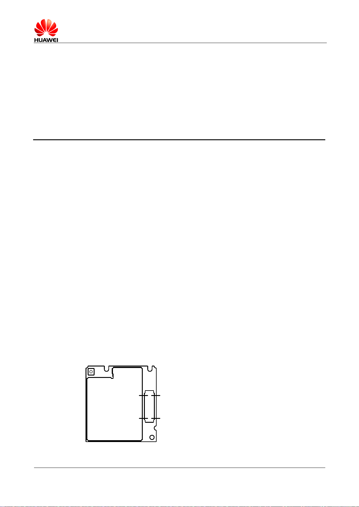
Dimensions (L x W x H): 35 mm x 32.5 mm x 3.05 mm
Figure 6-1 shows the dimensions.
Weight: 5.8 g
Issue 06 (2013-06-13)
Huawei Proprietary and Confidential
45
Page 46

HUAWEI MG323 GSM M2M Module
Hardware Guide
Mechanical Specifications
Copyright © Huawei Technologies Co., Ltd.
Figure 6-1 Dimensions of the MG323 module (unit: mm)
6.3 Dimensions of the B2B Connector
The MG323 module uses t he 50-pin B2B connector whose model is DF12C(3.0)50DS-0.5V(81) and whos e pin spacing is 0.5 mm to work with the conne ct or DF12E
(3.0)-50DP-0.5V (81) of the DF12 series (both conn ect or s ar e manufactured by
Hirose). For specific models, access http://www.hirose.com.
Figure 6-2 DF12C (manufactured by Hirose) used on the MG323 module
Issue 06 (2013-06-13)
Huawei Proprietary and Confidential
46
Page 47

HUAWEI MG323 GSM M2M Module
Hardware Guide
Mechanical Specifications
Copyright © Huawei Technologies Co., Ltd.
Figure 6-3 DF12E (manufactured by Hirose) recommended to be used with the MG323
module on the user interface board
Table 6-1 Ordered connector model and DF12 product series working with the MG323
module
Item Model
Connector model used
with the MG323 module
Connector model
recommended to be used
DF12C(3.0)-50DS-
0.5V(81)
DF12E(3.0)-50DP-
0.5V(81)
on the user interface
board
Stacking
HRS Number
Height (mm)
3.0 537-0694-9-81
3.0 537-0834-6-**
Issue 06 (2013-06-13)
Huawei Proprietary and Confidential
47
Page 48

HUAWEI MG323 GSM M2M Module
Hardware Guide
Mechanical Specifications
Copyright © Huawei Technologies Co., Ltd.
Figure 6-4 Dimensions of the connector used on the MG323 module (unit: mm)
6.4 MG323 Module Installation Description
Three structure fixing hole s ( diameter: 2 mm) are reserv ed in the M G323 module.
The holes are not sprayed w it h a coat ed i ns ulation and connected with the main
reference GND of the module, as shown in Figure 6-5 .
Figure 6-5 Structure fixing hole
You can insert machine screws through the st r ucture fixing holes and metal fasteners
and fasten with nuts to f irm ly c onnect t he M G 323 module to the user interface board
[1]. The metal fastener is placed between the MG323 module and user interface
Issue 06 (2013-06-13)
Huawei Proprietary and Confidential
48
Page 49

HUAWEI MG323 GSM M2M Module
Hardware Guide
Mechanical Specifications
Copyright © Huawei Technologies Co., Ltd.
board and functions as a brace an d c onnects the MG323 module and user interface
board through the reference GND. Below the user interface board, the nuts are used
to fasten the screws. Figure 6-6 shows the MG323 module installation.
Figure 6-6 MG323 module installation
[1]: Pay great attention to ESD protection when using the MG323 module. To ensure that the
working reference GND is connected to the MG323 module and user interface board properly,
you are recommended not to spray a coated insulation on the structure fixing hole (connecting
with the main reference GND of the user interfac e board) and connect the hole with the
MG323 module through the metal fastener or other low-resistance fastener.
Issue 06 (2013-06-13)
Huawei Proprietary and Confidential
49
Page 50

HUAWEI MG323 GSM M2M Module
Hardware Guide
Mechanical Specifications
Issue 06 (2013-06-13)
Huawei Proprietary and Confidential
Copyright © Huawei Technologies Co., Ltd.
50
6.5 Specification Selection for Fasteners
Protecting
from Screw
Loosening
To ensure that the MG323 module is firmly fixed on the interface board when using
the MG323 module, you are recommended to you use the M1.6 or M1.8 machine
screw. You can also customize the screws. The fastener components in the following
figures are recommended. The machine screw dimensions are M1.6×7.5×3.0×1.0. It
is recommended that you plate gold on the metal fastener. Figure 6-7 shows the
specific dimensions for the fastener components.
Figure 6-7 Machine screw dimensions
Page 51

HUAWEI MG323 GSM M2M Module
Hardware Guide
Mechanical Specifications
Copyright © Huawei Technologies Co., Ltd.
Figure 6-8 Nut dimensions
Figure 6-9 Metal fastener dimensions
Issue 06 (2013-06-13)
Huawei Proprietary and Confidential
51
Page 52

HUAWEI MG323 GSM M2M Module
Hardware Guide
Appendix A Circuits of Typical Interfaces
Issue 06 (2013-06-13)
Huawei Proprietary and Confidential
Copyright © Huawei Technologies Co., Ltd.
52
7 Appendix A Circuits of Typical Interfaces
22 μF
1μF100 nF330pF
Ferrite bea d
+
220 μF
+ + + +
220 μF 220 μF 220 μF 220 μF
LED_STA TUS
LED_STAT US
nF
nF
VBAT
c
e
b
470Ω
2.2K
0.1u
VCCA
VCCB
A1
B1
B2
B3
B4
A2
A3
A4
GND OE
UART1_DTR_MCU
UART1_TD_MCU
UART1_RD_MCU
UART1_RTS_MCU
UART1_DTR_MCU
UART1_TD_MCU
UART1_RD_MCU
UART1_RTS_MCU
UART1_DTR
UART1_DTR
UART1_TD
UART1_TD
UART1_RD
UART1_RD
UART1_RTS
UART1_ R TS
100nf 1uf
VGPIO
VGPIO
10K
VGPIO
VIO
VIO
b
c
e
b
c
e
0
RESET
Figure 7-1 Circuits of typical interfaces in the MG323 module
Page 53

HUAWEI MG323 GSM M2M Module
Hardware Guide
Appendix B Acronyms and Abbreviations
Copyright © Huawei Technologies Co., Ltd.
8 Appendix B Acronyms and Abbreviations
Acronym or Abbreviation Expansion
B2B Board-to-Board
CE European Conformity
CS Coding Scheme
CSD Circuit Switched Data
DC Direct Current
DCE Data Circuit-terminating Equipment
DMA Direct Memory Access
DTE Data Terminal Equipment
EMC Electromagnetic Compatibility
ESD Electrostatic Discharge
EU European Union
FCC Federal Communications Commission
FDD-TDMA
GMSK Gaussian Minimum Shift Keying
GPRS General Packet Radio Service
ISO International Standards Organization
Frequency Division Duplexing–time Division Multiple
Access
LCP Liquid Crystal Polyester
LDO Low-Dropout
LED Light-emitting Diode
MCP Multi-chip Package
NTC Negative Temperature Coefficient
Issue 06 (2013-06-13)
Huawei Proprietary and Confidential
53
Page 54

HUAWEI MG323 GSM M2M Module
Hardware Guide
Appendix B Acronyms and Abbreviations
Copyright © Huawei Technologies Co., Ltd.
Acronym or Abbreviation Expansion
PBCCH Packet Broadcast Control Channel
PCB Printed Circuit Board
PDU Protocol Data Unit
RF Radio Frequency
RoHS
Restriction of the Use of Certain Hazardous
Substances
RTC Real-time Clock
SIM Subscriber Identity Module
TTL Transistor-transistor Logic
TVS Transient Voltage Suppressor
UART Universal Asynchronous Receiver-transmitter
VSWR Voltage Standing Wave Ratio
Issue 06 (2013-06-13)
Huawei Proprietary and Confidential
54
 Loading...