

Page 1

HUAWEI MC509 CDMA LGA Module
Hardware Guide
Issue
01
Date
2011-04-08
Page 2

Huawei Technologies Co., Ltd. provides customers with comprehensive technical support and service. For
any assistance, please contact our local office or company headquarters.
Huawei Technologies Co., Ltd.
Huawei Industrial Base, Bantian, Longgang, Shenzhen 518129, People’s Republic of China
Tel: +86-755-28780808 Global Hotline: +86-755-28560808 Website: www.huawei.com
E-mail: mobile@huawei.com
Please refer color and shape to product. Huawei reserves the right to make changes or improvements to any
of the products without prior notice.
Copyright © Huawei Technologies Co., Ltd. 2011. All rights reserved.
No part of this document may be reproduced or transmitted in any form or by any means without prior written
consent of Huawei Technologies Co., Ltd.
The product described in this manual may include copyrighted software of Huawei Technologies Co., Ltd and
possible licensors. Customers shall not in any manner reproduce, distribute, modify, decompile, disassemble,
decrypt, extract, reverse engineer, lease, assign, or sublicense the said software, unless such restrictions
are prohibited by applicable laws or such actions are approved by respective copyright holders under
licenses.
Trademarks and Permissions
, , and
Other trademarks, product, service and company names mentioned are the property of their respective
owners.
are trademarks or registered trademarks of Huawei Technologies Co., Ltd.
Notice
Some features of the product and its accessories described herein rely on the software installed, capacities
and settings of local network, and may not be activated or may be limited by local network operators or
network service providers, thus the descriptions herein may not exactly match the product or its accessories
you purchase.
Huawei Technologies Co., Ltd reserves the right to change or modify any information or specifications
contained in this manual without prior notice or obligation.
NO WARRANTY
THE CONTENTS OF THIS MANUAL ARE PROVIDED “AS IS”. EXCEPT AS REQUIRED BY APPLICABLE
LAWS, NO WARRANTIES OF ANY KIND, EITHER EXPRESS OR IMPLIED, INCLUDING BUT NOT
LIMITED TO, THE IMPLIED WARRANTIES OF MERCHANTABILITY AND FITNESS FOR A PARTICULAR
PURPOSE, ARE MADE IN RELATION TO THE ACCURACY, RELIABILITY OR CONTENTS OF THIS
MANUAL.
TO THE MAXIMUM EXTENT PERMITTED BY APPLICABLE LAW, IN NO CASE SHALL HUAWEI
TECHNOLOGIES CO., LTD BE LIABLE FOR ANY SPECIAL, INCIDENTAL, INDIRECT, OR
CONSEQUENTIAL DAMAGES, OR LOST PROFITS, BUSINESS, REVENUE, DATA, GOODWILL OR
ANTICIPATED SAVINGS.
Import and Export Regulations
Customers shall comply with all applicable export or import laws and regulations and will obtain all necessary
governmental permits and licenses in order to export, re-export or import the product mentioned in this
manual including the software and technical data therein
Page 3
HUAWEI MC509 CDMA LGA Module
Hardware Guide
About This Document
Issue 01 (2011-04-08)
Huawei Proprietary and Confidential
Copyright © Huawei Technologies Co., Ltd.
3
History
Version
Date
Chapter
Descriptions
01
2011-04-08
Creation
About This Document
Page 4
HUAWEI MC509 CDMA LGA Module
Hardware Guide
About This Document
Issue 01 (2011-04-08)
Huawei Proprietary and Confidential
Copyright © Huawei Technologies Co., Ltd.
4
Summary
Chapter
Details
1 Introduction
Describes the short introduction of the
product.
2 Overall Description
Describes the Function overview, Circuit
Block Diagram and Application Block
Diagram of the product.
3 Description of the Application
Interfaces
Describes the external application
interfaces of the product.
4 RF Specifications
Describes the RF specifications of the
product.
5 Electrical and Reliability Features
Describes the electrical and reliability
features of the interfaces in the product.
6 Mechanical Specifications
Describes the Dimensions, Label and
Packing System of the product.
7 Certifications
Describes the certifications of the
product.
8 Safety Information
Lists the safety information of using the
product.
9 Appendix A Circuit of Typical
InterfacesI
Lists the circuit of typical interface of the
product.
10 Appendix B Acronyms and
Abbreviations
Lists the acronyms and abbreviations
mentioned in this document.
This document provides information about the major functions, supported services,
system architecture, and technical references of HUAWEI MC509 CDMA LGA
Module.
Packing System
Certifications
Environmental Protection Certification and Test
National Compulsory Certification
The following table lists the contents of this document.
Page 5

HUAWEI MC509 CDMA LGA Module
Hardware Guide
Content
Issue 01 (2011-04-08)
Huawei Proprietary and Confidential
Copyright © Huawei Technologies Co., Ltd.
5
Content
1 Introduction.................................................................................................................................... 8
2 Overall Description ...................................................................................................................... 9
2.1 About This Chapter ........................................................................................................................... 9
2.2 Function Overview............................................................................................................................ 9
2.3 Circuit Block Diagram ...................................................................................................................... 11
2.4 Application Block Diagram ............................................................................................................. 12
3 Description of the Application Interfaces .............................................................................. 13
3.1 About This Chapter ......................................................................................................................... 13
3.2 LGA Interface ................................................................................................................................. 13
3.3 Power Interface .............................................................................................................................. 22
3.3.1 Overview ................................................................................................................................ 22
3.3.2 VBAT Interface ....................................................................................................................... 23
3.3.3 VCOIN Interface .................................................................................................................... 24
3.3.4 Output Power Supply Interface ............................................................................................. 25
3.4 Signal Control Interface .................................................................................................................. 26
3.4.1 Overview ................................................................................................................................ 26
3.4.2 Input Signal Control Pins ....................................................................................................... 27
3.4.3 Output Signal Control Pin (TBD) ........................................................................................... 30
3.4.4 WAKEUP_IN Signal............................................................................................................... 30
3.4.5 WAKEUP_OUT Signal............................................................................................................. 30
3.5 UART Interface ............................................................................................................................... 31
3.5.1 Overview ................................................................................................................................ 31
3.5.2 Circuit Recommended for the UART Interface ...................................................................... 32
3.6 USB Interface ................................................................................................................................. 33
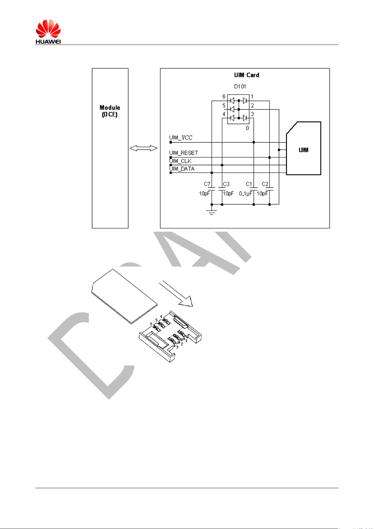
3.7 UIM Card Interface ......................................................................................................................... 35
3.7.1 Overview ................................................................................................................................ 35
3.7.2 Circuit Recommended for the UIM Card Interface ................................................................ 35
3.7.3 ESD Protection for the UIM Card Interface ........................................................................... 37
3.8 Audio Interface ............................................................................................................................... 37
3.8.1 Analogue Audio ...................................................................................................................... 37
3.8.2 Digital Audio ........................................................................................................................... 39
3.9 General Purpose I/O Interface ....................................................................................................... 40
Page 6

HUAWEI MC509 CDMA LGA Module
Hardware Guide
Content
Issue 01 (2011-04-08)
Huawei Proprietary and Confidential
Copyright © Huawei Technologies Co., Ltd.
6
3.10 JTAG Interface ............................................................................................................................. 41
3.11 RF Antenna Interface.................................................................................................................... 41
3.12 NC Pins ........................................................................................................................................ 42
4 RF Specifications ......................................................................................................................... 43
4.1 About This Chapter ......................................................................................................................... 43
4.2 Antenna Installation Guidelines ...................................................................................................... 43
4.3 Operating Frequencies ................................................................................................................... 43
4.4 Conducted RF Measurement ......................................................................................................... 44
4.4.1 Test Environment ................................................................................................................... 44
4.4.2 Test Standards ....................................................................................................................... 44
4.5 Conducted Rx Sensitivity and Tx Power ........................................................................................ 44
4.5.1 Conducted Receive Sensitivity .............................................................................................. 44
4.5.2 Conducted Transmit Power ................................................................................................... 45
4.6 Antenna Design Requirements ...................................................................................................... 45
4.6.1 Antenna Design Indicators..................................................................................................... 45
4.6.2 Interference ........................................................................................................................... 47
4.6.3 CDMA Antenna Requirements............................................................................................... 47
4.6.4 Radio Test Environment ........................................................................................................ 48
5 Electrical and Reliability Features ........................................................................................... 49
5.1 About This Chapter ......................................................................................................................... 49
5.2 Extreme Working Conditions .......................................................................................................... 49
5.3 Working and Storage Temperatures and Humidity ........................................................................ 50
5.4 Electrical Features of Application Interfaces .................................................................................. 50
5.5 Power Supply Features .................................................................................................................. 51
5.5.1 Input Power Supply ............................................................................................................... 51
5.5.2 Power Consumption .............................................................................................................. 52
5.6 Reliability Features ......................................................................................................................... 52
5.7 EMC and ESD Features ................................................................................................................. 54
6 Mechanical Specifications ......................................................................................................... 55
6.1 About This Chapter ......................................................................................................................... 55
6.2 Dimensions and interfaces ............................................................................................................. 55
6.3 PCB Pad Design ............................................................................................................................ 56
6.4 Label ............................................................................................................................................... 57
6.5 Packing System.............................................................................................................................. 58
7 Certifications ................................................................................................................................ 59
7.1 About This Chapter ......................................................................................................................... 59
7.2 Environmental Protection Certification and Test ............................................................................ 60
7.2.1 RoHS ..................................................................................................................................... 60
7.2.2 WEEE .................................................................................................................................... 61
7.2.3 PVC-free ................................................................................................................................ 62
Page 7

HUAWEI MC509 CDMA LGA Module
Hardware Guide
Content
Issue 01 (2011-04-08)
Huawei Proprietary and Confidential
Copyright © Huawei Technologies Co., Ltd.
7
7.3 National Compulsory Certification .................................................................................................. 62
7.3.1 Product Certification .............................................................................................................. 62
7.3.2 Importance of Product Certification ....................................................................................... 62
7.3.3 Product Certification Test Items ............................................................................................. 62
7.3.4 Product Certification Classifications ...................................................................................... 63
7.3.5 Certification Modes ................................................................................................................ 63
7.3.6 Certification Types ................................................................................................................. 64
7.3.7 Guide to Product Certification ............................................................................................... 72
7.4 GCF and PTCRB............................................................................................................................ 73
7.4.1 GCF Certification ................................................................................................................... 73
7.4.2 PTCRB Certification .............................................................................................................. 75
7.4.3 Overall-System Certification .................................................................................................. 75
8 Safety Information ...................................................................................................................... 79
8.1 Interference .................................................................................................................................... 79
8.2 Medical Device ............................................................................................................................... 79
8.3 Area with Inflammables and Explosives ......................................................................................... 79
8.4 Traffic Security ................................................................................................................................ 80
8.5 Airline Security ................................................................................................................................ 80
8.6 Safety of Children ........................................................................................................................... 80
8.7 Environment Protection .................................................................................................................. 80
8.8 WEEE Approval .............................................................................................................................. 80
8.9 RoHS Approval ............................................................................................................................... 80
8.10 Laws and Regulations Observance ............................................................................................. 81
8.11 Care and Maintenance ................................................................................................................. 81
8.12 Emergency Call ............................................................................................................................ 81
8.13 Specific Absorption Rate (SAR) ................................................................................................... 81
8.14 Regulatory Information ................................................................................................................. 82
8.14.1 CE Approval (European Union) ........................................................................................... 82
8.14.2 FCC Statement .................................................................................................................... 82
9 Appendix A Circuit of Typical Interfaces .............................................................................. 83
10 Appendix B Acronyms and Abbreviations .......................................................................... 85
Page 8
HUAWEI MC509 CDMA LGA Module
Hardware Guide
Introduction
Issue 01 (2011-04-08)
Huawei Proprietary and Confidential
Copyright © Huawei Technologies Co., Ltd.
8
1 Introduction
Product name
RF Band
Bandwidth
MC509
CDMA/EVDO 1900/800
MHz
Data only
Telematics
Analog voice input function
×
√
Analog voice output
function
×
√
PCM voice function
×
√
This document describes the hardware application interfaces and air interfaces that
are provided when the HUAWEI MC509 CDMA LGA Module (hereinafter referred to
as the MC509 module) is used.
This document helps you to understand the interface specifications, electrical
features, and related product information of the MC509 module. To facilitate its use in
different fields, relevant development guide documents are also provided with the
module, which can be obtained from the Huawei website.
CDMA/EVDO 1900/800 MHz(Data only or Telematics)
MC509 model has two editions: Data only or Telematics. Data only does not support
the voice function.
Page 9
HUAWEI MC509 CDMA LGA Module
Hardware Guide
Overall Description
Issue 01 (2011-04-08)
Huawei Proprietary and Confidential
Copyright © Huawei Technologies Co., Ltd.
9
2.1 About This Chapter
Feature
Description
Physical
Features
Dimensions (L × W × H): 30mm×30mm×2.6mm
Weight about 5.5g
Working Bands
CDMA2000 1x, CDMA2000 EV-DO Rev 0, CDMA2000 EV-DO
Rev A
Supports BC0(800MHz band), BC1(1900MHz band) (Data only
or Telematics)
Working
Temperature
Normal working temperature: –20°C ~ +70°C
Extreme working temperatures: –30°C ~ –20°C and +70°C ~
+75°C
Ambient
Temperature
for Storage
–40°C ~ 85°C
Power Voltage
3.3V ~ 4.2V (3.8V is recommended.)
AT Commands
See the HUAWEI MC509 CDMA LGA Module AT Command
Interface Specification.
This chapter gives a general description of the MC509 module and provides:
Function Overview
Circuit Block Diagram
Application Block Diagram
2 Overall Description
2.2 Function Overview
Table 2-1 Feature
Page 10
HUAWEI MC509 CDMA LGA Module
Hardware Guide
Overall Description
Issue 01 (2011-04-08)
Huawei Proprietary and Confidential
Copyright © Huawei Technologies Co., Ltd.
10
Feature
Description
Application
Interface (145pin LGA
interface)
Universal Asynchronous Receiver-Transmitter (UART)
Supporting 8-wire UART
One standard user interface Module (UIM) card (3V or 1.8V)
Audio (OPTION): (only telematics version supports this function)
For detailed information about the working bands supported, see
错误!未找到引用源。.
2×Micphone in
1×Speaker out
1×handset out
1×PCM
USB 2.0(full speed)
Power on/off
Reset
Wakeup In
Wakeup out (TBD)
Light-emitting Diode (LED)
Configurable General-purpose I/O (GPIO)
RF pad
Power
SMS
New message alert, text message receiving, and text message
sending
Management of text messages: read messages, delete
messages, storage status, and message list
Support for the Protocol Data Unit (PDU) mode
Data Services
CDMA2000 1X: UL/DL: 153.6kbps
CDMA2000 1X/EVDO rev.0: UL 153.6kbps DL 2.4Mbps
CDMA2000 1X/EVDO rev A: UL 1.8Mbps DL 3.1Mbps
Security
(TBD)
Internet
Protocols
TCP/IP, UDP/IP, PPP protocol
Applications
(TBD)
Page 11
HUAWEI MC509 CDMA LGA Module
Hardware Guide
Overall Description
Issue 01 (2011-04-08)
Huawei Proprietary and Confidential
Copyright © Huawei Technologies Co., Ltd.
11
Feature
Description
Certification
Information
Restriction of the use of certain Hazardous Substances
(RoHS)
Federal Communications Commission (FCC)
China Compulsory Certification(CCC)
China Telecommunications Equipment Network Access
Approval(CTA)
Waste Electrical and Electronic Equipment Directive(WEEE)
2.3 Circuit Block Diagram
Figure 2-1 shows the circuit block diagram of the MC509 module. The application
block diagram and major functional units of the MC509 module contain the following
parts:
Qualcomm QSC chip
Multi-chip package (MCP) memory
RF Circuit
Figure 2-1 Circuit block diagram of the MC509 module
Only telematics version supports the audio function.
Page 12
HUAWEI MC509 CDMA LGA Module
Hardware Guide
Overall Description
Issue 01 (2011-04-08)
Huawei Proprietary and Confidential
Copyright © Huawei Technologies Co., Ltd.
12
2.4 Application Block Diagram
UART Interface:
The module supports 3-line or 5-line or full serial port
interface.
USB Interface:
The USB interface supports USB 2.0 full speed standard.
UIM Interface:
The UIM interface provides the interface for a UIM card. The
UIM card can be inserted into the host side.
Power Supply:
DC 3.8V is recommended.
Audio Interface:
The module supports one speaker output, two microphone,
one handset, one speaker and one PCM interface (only
telematics version supports the audio function).
Figure 2-2 Application block diagram of the MC509 module
Page 13

HUAWEI MC509 CDMA LGA Module
Hardware Guide
Description of the Application Interfaces
Issue 01 (2011-04-08)
Huawei Proprietary and Confidential
Copyright © Huawei Technologies Co., Ltd.
13
3 Description of the Application Interfaces
3.1 About This Chapter
This chapter mainly describes the external application interfaces of the MC509
module, including:
LGA Interface
Power Interface
Signal Control Interface
UART Interface
USB Interface
UIM Card Interface
Audio Interface
General Purpose I/O Interface
JTAG Interface
RF Antenna Interface
NC Pins
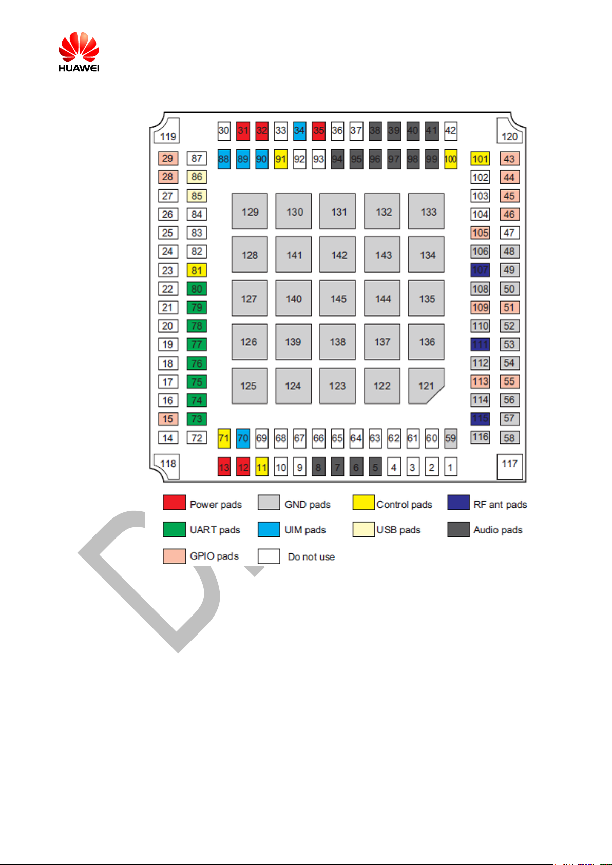
3.2 LGA Interface
The MC509 module uses a 145-pin LGA as its external interface. For details about
the module and dimensions of the LGA, see “6.2 Dimensions and interfaces”.
If DTE supports Huawei LGA module, such as module with system of CDMA, TDSCDMA or HSPA +, you can refer to Huawei LGA Migration Guide to get the details.
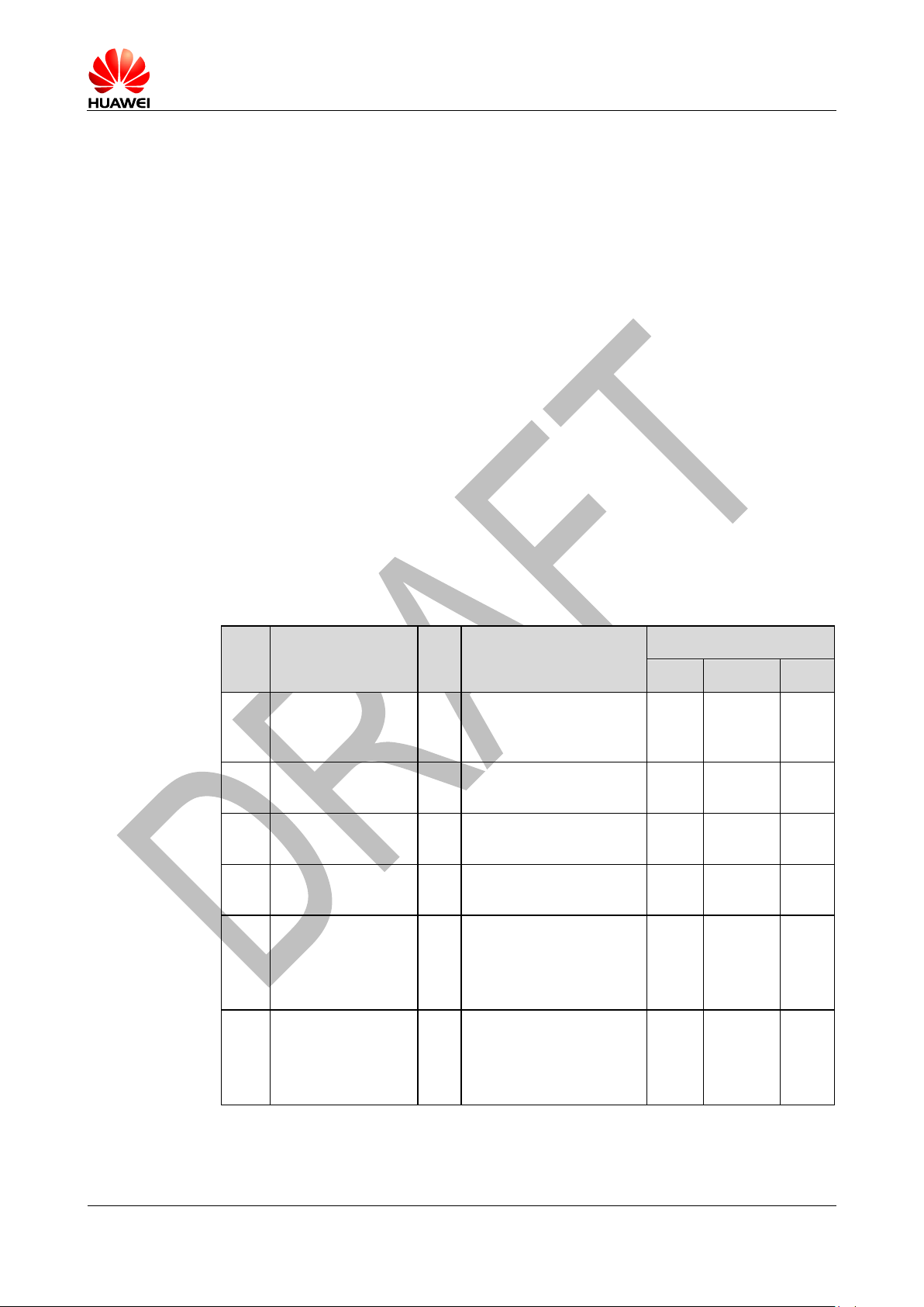
Table 3-1 shows the definitions of pins on the 145-pin signal interface of the MC509
module.
Page 14
HUAWEI MC509 CDMA LGA Module
Hardware Guide
Description of the Application Interfaces
Issue 01 (2011-04-08)
Huawei Proprietary and Confidential
Copyright © Huawei Technologies Co., Ltd.
14
Table 3-1 Definitions of pins on the LGA interface
PIN
No.
Pin Name
I/O
Description
DC Characteristics (V)
Normal
MUX
Min
Typical
Max
1
NC - -
Not connected, please
keep this pin open
- - -
2
NC - -
Not connected, please
keep this pin open
- - -
3
NC - -
Not connected, please
keep this pin open
- - -
4
NC - -
Not connected, please
keep this pin open
- - 5
PCM_SYNC
GPIO
I/O
PCM interface sync
-0.3
2.6
2.9 6 PCM_DIN
GPIO
I
PCM I/F data in
-0.3
2.6
2.9 7 PCM_DOUT
GPIO
O
PCM I/F data out
-0.3
2.6
2.9 8 PCM_CLK
GPIO
I/O
PCM interface clock
-0.3
2.6
2.9
9
NC - -
Not connected, please
keep this pin open
- - -
10
NC - -
Not connected, please
keep this pin open
- - 11
WAKEUP_IN
GPIO
I
Host to wake up Module
-0.3
2.6
2.9
12
VBAT
- P Power supply input
3.3
3.8
4.2
13
VBAT
- P Power supply input
3.3
3.8
4.2
14
PS_HOLD
-
-
This input high to keep
power on, low to shut
down.
-
1.8
-
15
Reserved
- - - - -
-
16
NC - -
Not connected, please
keep this pin open
- - -
17
NC - -
Not connected, please
keep open
- - -
18
NC - -
Not connected, please
keep this pin open
- - -
19
NC - -
Not connected, please
keep this pin open
- - -
20
NC - -
Not connected, please
keep this pin open
- - -
Page 15
HUAWEI MC509 CDMA LGA Module
Hardware Guide
Description of the Application Interfaces
Issue 01 (2011-04-08)
Huawei Proprietary and Confidential
Copyright © Huawei Technologies Co., Ltd.
15
PIN
No.
Pin Name
I/O
Description
DC Characteristics (V)
Normal
MUX
Min
Typical
Max
21
NC - -
Not connected, please
keep this pin open
- - -
22
NC - -
Not connected, please
keep this pin open
- - -
23
NC - -
Not connected, please
keep this pin open
- - -
24
NC - -
Not connected, please
keep this pin open
- - -
25
NC - -
Not connected, please
keep this pin open
- - -
26
NC - -
Not connected, please
keep this pin open
- - -
27
NC - -
Not connected, please
keep this pin open
- - 28
Reserved
- - - - -
-
29
Reserved
- - - - -
-
30
JTAG_TMS
- I JTAG Test mode select
-0.3
2.6
2.9
31
VCC_EXT2
- P 2.6V POWER output
-
2.6
-
32
VCC_EXT1
- P 1.8V POWER output
-
1.8
-
33
NC - -
Not connected, please
keep this pin open
- - -
34
UIM_VCC
-
P
Power supply for UIM
card
-0.3
1.8/2.8
5
2.1/3.1
5
35
VCOIN
- P Coin cell input
1.5
3.0
3.25
36
JTAG_TRST_N
-
I
JTAG reset
-0.3
2.6
2.9
37
NC - -
Not connected, please
keep this pin open
- - -
38
MIC2_P
-
I
(Only telematics version
supports audio function,
Data only version does
not support this function)
Positive pole of the input
of audio interface 2
- - -
Page 16
HUAWEI MC509 CDMA LGA Module
Hardware Guide
Description of the Application Interfaces
Issue 01 (2011-04-08)
Huawei Proprietary and Confidential
Copyright © Huawei Technologies Co., Ltd.
16
PIN
No.
Pin Name
I/O
Description
DC Characteristics (V)
Normal
MUX
Min
Typical
Max
39
MIC2_N
-
I
(Only telematics version
supports audio function,
Data only version does
not support this function)
Negative pole of the input
of audio interface 2
- - -
40
MIC1_P
-
I
(Only telematics version
supports audio function ,
Data only version does
not support this function)
Positive pole of the input
of audio interface 1
- - -
41
MIC1_N
-
I
(Only telematics version
supports audio function ,
Data only version does
not support this function)
Negative pole of the input
of audio interface 1
- - -
42
JTAG_TCK
-
I
JTAG clock input
-0.3
2.6
2.9
43
Reserved
- - - - -
-
44
GPIO
-
I/O
General I/O pin. The
function of these pins has
not been defined
-0.3
2.6
2.9
45
W_DISABLE
-
I
Close wireless
communications
-0.3
2.6
2.9
46
GPIO
-
I/O
General I/O pins. The
function of these pins has
not been defined
-0.3
2.6
2.9
47
NC - -
Not connected, please
keep this pin open
- - 48
GND
- - GND
- - -
49
GND
- - GND
- - -
50
GND
- - GND
- - -
51
GPIO
-
I/O
General I/O pins. The
function of these pins has
not been defined
-0.3
2.6
2.9
52
GND
- - GND
- - -
53
GND
- - GND
- - -
54
GND
- - GND
- - -
Page 17
HUAWEI MC509 CDMA LGA Module
Hardware Guide
Description of the Application Interfaces
Issue 01 (2011-04-08)
Huawei Proprietary and Confidential
Copyright © Huawei Technologies Co., Ltd.
17
PIN
No.
Pin Name
I/O
Description
DC Characteristics (V)
Normal
MUX
Min
Typical
Max
55
GPIO
-
I/O
General I/O pins. The
function of these pins has
not been defined
-0.3
2.6
2.9
56
GND
- - GND
- - -
57
GND
- - GND
- - -
58
GND
- - GND
- - -
59
GND
- - GND
- - -
60
NC - -
Not connected, please
keep this pin open
- - -
61
NC - -
Not connected, please
keep this pin open
- - -
62
NC - -
Not connected, please
keep this pin open
- - -
63
NC - -
Not connected, please
keep this pin open
- - -
64
NC - -
Not connected, please
keep this pin open
- - -
65
NC - -
Not connected, please
keep this pin open
- - -
66
NC - -
Not connected, please
keep this pin open
- - -
67
NC - -
Not connected, please
keep this pin open
- - -
68
NC - -
Not connected, please
keep this pin open
- - -
69
NC - -
Not connected, please
keep this pin open
- - -
70
NC - -
Not connected, please
keep this pin open
- - -
71
WAKEUP_OUT
GPIO
O
Module to wake up the
host
-0.3
2.6
2.9
72
JTAG_TDO
- Z JTAG test data output
-0.3
2.6
2.9
73
UART_DSR
GPIO
O
UART Data Set Ready
-0.3
2.6
2.9
74
UART_RTS
GPIO
O
UART Ready for receive
-0.3
2.6
2.9
75
UART_DCD
GPIO
O
UART Data Carrier Detect
-0.3
2.6
2.9
76
UART_TX
GPIO
O
UART transmit output
-0.3
2.6
2.9
Page 18
HUAWEI MC509 CDMA LGA Module
Hardware Guide
Description of the Application Interfaces
Issue 01 (2011-04-08)
Huawei Proprietary and Confidential
Copyright © Huawei Technologies Co., Ltd.
18
PIN
No.
Pin Name
I/O
Description
DC Characteristics (V)
Normal
MUX
Min
Typical
Max
77
UART_RING
GPIO
O
UART Ring Indicator
-0.3
2.6
2.9
78
UART_RX
GPIO
I
UART receive data input
-0.3
2.6
2.9
79
UART_DTR
GPIO
I
Data Terminal Ready
-0.3
2.6
2.9
80
UART_CTS
GPIO
I
UART Clear to Send
-0.3
2.6
2.9
81
POWER_ON_OFF
-
I
System power-on or
power-off
-
Pulled
up on
chip
-
82
NC - -
Not connected, please
keep this pin open
- - -
83
NC - -
Not connected, please
keep this pin open
- - -
84
NC - -
Not connected, please
keep this pin open
- - 85
USB_DM
-
I/O
Full-speed USB D-
- - -
86
USB_DP
-
I/O
Full-speed USB D+
- - -
87
JTAG_TDI
-
I
JTAG test data input
-0.3
2.6
2.9
88
UIM_RESET
- O UIM reset
-0.3
1.8/2.8
5
2.1/3.1
5
89
UIM_DATA
-
I/O
UIM Data
-0.3
1.8/2.8
5
2.1/3.1
5
90
UIM_CLK
- O UIM Clock
-0.3
1.8/2.8
5
2.1/3.1
5
91
LED_STATUS
-
I
Status indicator
SINK current source
Driver strength: 10mA
- - 92
NC - -
Not connected, please
keep this pin open
- - 93
JTAG_RTCK
- I JTAG return clock
-0.3
2.6
2.9
94
NC -
Not connected, please
keep this pin open
- - -
95
NC -
Not connected, please
keep this pin open
- - -
Page 19

HUAWEI MC509 CDMA LGA Module
Hardware Guide
Description of the Application Interfaces
Issue 01 (2011-04-08)
Huawei Proprietary and Confidential
Copyright © Huawei Technologies Co., Ltd.
19
PIN
No.
Pin Name
I/O
Description
DC Characteristics (V)
Normal
MUX
Min
Typical
Max
96
EAR_OUT_N
-
O
(Only telematics version
supports audio function ,
Data only version does
not support this function)
Negative pole of the
output of Earphone
interface
- - 97
EAR_OUT_P
-
O
(Only telematics version
supports audio function ,
Data only version does
not support this function)
Positive pole of the output
of Earphone interface
- - -
98
SPKR_OUT_P
-
O
(Only telematics version
supports audio function,
Data only version does
not support this function)
Positive pole of the output
of speaker interface
- - -
99
SPKR_OUT_N
-
O
(Only telematics version
supports audio function,
Data only version does
not support this function)
Negative pole of the
output of speaker
interface
- - -
100
RESIN_N
- I Reset module.
-0.3
1.8
2.1
101
LED_MODE
- I Mode indicator
SINK current source
Driver strength: 10 mA
- - -
102
NC - -
Not connected, please
keep this pin open
- - -
103
NC - -
Not connected, please
keep this pin open
- - -
104
NC - -
Not connected, please
keep this pin open
- - -
105
GPIO
-
I/O
General I/O pins. The
function of these pins has
not been defined.
-0.3
2.6
2.9
106
GND
- - GND
- - -
107
MAIN_ANT
-
-
RF main antenna
interface
- - -
Page 20
HUAWEI MC509 CDMA LGA Module
Hardware Guide
Description of the Application Interfaces
Issue 01 (2011-04-08)
Huawei Proprietary and Confidential
Copyright © Huawei Technologies Co., Ltd.
20
PIN
No.
Pin Name
I/O
Description
DC Characteristics (V)
Normal
MUX
Min
Typical
Max
108
GND
- - GND
- - -
109
GPIO
-
I/O
General I/O pins. The
function of these pins has
not been defined
-0.3
2.6
2.9
110
GND
- - GND
- - -
111
GPS_ANT
-
-
RF GPS antenna
interface
- - 112
GND
- - GND
- - -
113
GPIO
-
I/O
General I/O pins. The
function of these pins has
not been defined
-0.3
2.6
2.9
114
GND
- - GND
- - -
115
AUX_ANT
-
-
RF divert antenna
interface
- - 116
GND
- - GND
- - -
117
NC
-
-
Not connected, please
keep this pin open
- - 118
NC
-
-
Not connected, please
keep this pin open
- - 119
NC
-
-
Not connected, please
keep this pin open
- - 120
NC
-
-
Not connected, please
keep this pin open
- - 121
GND
- - GND
- - -
122
GND
- - GND
- - -
123
GND
- - GND
- - -
124
GND
- - GND
- - -
125
GND
- - GND
- - -
126
GND
- - GND
- - -
127
GND
- - GND
- - -
128
GND
- - GND
- - -
129
GND
- - GND
- - -
130
GND
- - GND
- - -
131
GND
- - GND
- - -
Page 21
HUAWEI MC509 CDMA LGA Module
Hardware Guide
Description of the Application Interfaces
Issue 01 (2011-04-08)
Huawei Proprietary and Confidential
Copyright © Huawei Technologies Co., Ltd.
21
PIN
No.
Pin Name
I/O
Description
DC Characteristics (V)
Normal
MUX
Min
Typical
Max
132
GND
- - GND
- - -
133
GND
- - GND
- - -
134
GND
- - GND
- - -
135
GND
- - GND
- - -
136
GND
- - GND
- - -
137
GND
- - GND
- - -
138
GND
- - GND
- - -
139
GND
- - GND
- - -
140
GND
- - GND
- - -
141
GND
- - GND
- - -
142
GND
- - GND
- - -
143
GND
- - GND
- - -
144
GND
- - GND
- - -
145
GND
- - GND
- - -
P indicates power pins; I indicates pins for digital signal input; O indicates pins for digital
signal output.
The NC (Not Connected) pins are internally connected to the module. Therefore, these pins
should not be used, otherwise they may cause problems. Please contact us for more
details about this information.
When the MC509 module works on master mode, PCM_CLK and PCM_SYNC pins are in
the output status
Figure 3-1 shows the sequence of pins on the 145-pin signal interface of the MC509
module.
Page 22
HUAWEI MC509 CDMA LGA Module
Hardware Guide
Description of the Application Interfaces
Issue 01 (2011-04-08)
Huawei Proprietary and Confidential
Copyright © Huawei Technologies Co., Ltd.
22
Figure 3-1 Bottom view of sequence of LGA interface pins
3.3 Power Interface
3.3.1 Overview
The power supply part of the MC509 module contains:
VBAT PIN for the power supply
VCOIN PIN for the standby power supply of the real-time clock (RTC)
VCC_EXT1 PIN for external power output
VCC_EXT2 PIN for external power output
UIM_VCC PIN for UIM card power output
Page 23
HUAWEI MC509 CDMA LGA Module
Hardware Guide
Description of the Application Interfaces
Issue 01 (2011-04-08)
Huawei Proprietary and Confidential
Copyright © Huawei Technologies Co., Ltd.
23
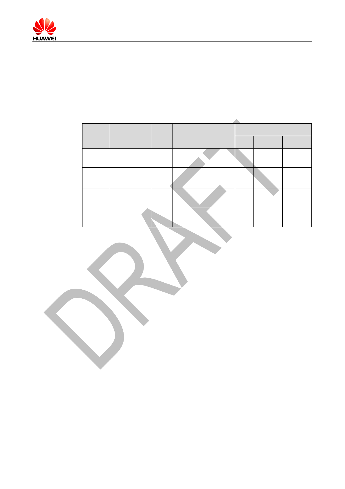
Table 3-2 lists the definitions of the pins on the power supply interface.
Pin No.
Signal Name
I/O
Description
DC Characteristics (V)
Min
Typical
Max
12, 13
VBAT
P
Pins for power
voltage input
3.3
3.8
4.2
48, 49, 50,
52, 53, 54,
56, 57, 58,
59, 106,
108, 110,
112, 114,
116
GND
-
GND
- - -
35
VCOIN
P
Pin for standby
power input of
the RTC
1.5
3.0
3.25
32
VCC_EXT1
P
Pin for external
power output
-
2.6 - 31
VCC_EXT2
P
Pin for external
power output
-
1.8 - 34
UIM_VCC
P
Power supply for
UIM card
-0.3
1.8/2.85
2.1/3.15
121~145
GND
-
Thermal Ground
Pad
- - -
Table 3-2 Definitions of the pins on the power supply interface
3.3.2 VBAT Interface
When the MC509 module works normally, power is supplied through the VBAT pins
and the voltage ranges from 3.3V to 4.2V (typical value: 3.8V). The 145-pin LGA
provides two VBAT pins and sixteen GND pins for external power input. To ensure
that the MC509 module works normally, all the pins must be used efficiently.
When the MC509 module is used for different external applications, pay special
attention to the design for the power supply. When the MC509 module transmits
signals at the maximum power, the transient current may reach the transient peak
value of about 1.5A due to the differences in actual network environments. In this
case, the VBAT voltage drops. Make sure that the voltage does not decrease below
3.3V in any case. Otherwise, exceptions such as restart of the MC509 module may
occur.
A low-dropout (LDO) regulator or switch power with current output of more than 1.5A
is recommended for external power supply. Furthermore, a 220uF or above energy
storage capacitor is connected in parallel at the power interface of the MC509
module.
Page 24
HUAWEI MC509 CDMA LGA Module
Hardware Guide
Description of the Application Interfaces
Issue 01 (2011-04-08)
Huawei Proprietary and Confidential
Copyright © Huawei Technologies Co., Ltd.
24
SMPL timer setting
Capacitor value
Capacitor package
0.5 sec
1.5μF
0805
1.0 sec
3.3μF
0805
1.5 sec
4.7μF
0805
2.0 sec
6.8μF
1206
For detailed information about power supply design and printed circuit board (PCB) design,
see the HUAWEI Module Power Supply Design Guide and the HUAWEI LGA Module PCB
Interconnection Design Guide
3.3.3 VCOIN Interface
VCOIN pin of MC509 module is used as backup power from the 3 V coin cell for
SMPL, RTC, and 32 kHz crystal oscillator backup; a capacitor (rather than a coin cell)
can be used if only SMPL is supported. Used as an analog output for coin cell or
capacitor charging.
Sudden momentary power loss
If the monitored VBAT drops out-of-range (<3.3V nominal), the SMPL feature may
initiate a power-on sequence without software intervention, and then VBAT returns inrange within a programmable interval of between 0.5 and 2.0 seconds. SMPL
achieves immediate and automatic recovery from momentary power loss. A valid
voltage on VCOIN is required to run the SMPL timer. If a capacitor is used instead of
a coin, it must be connected between VCOIN and the ground. The capacitor must be
charged to operate properly as the SMPL power source. The capacitor value
depends on the SMPL timer setting.
Table 3-3 Keep-alive capacitor values vs.SMPL timer settings
If the SMPL counter expires without VBAT returning to its valid range, the MC509
must undergo the normal power-on sequence whenever the VBAT is detected.
Real-time clock
If RTC is used, a manganese-lithium rechargeable battery is recommended, for
example, the SII Micro Parts HB-414 and the Panasonic ML-series. Two sets of coin
cell specifications are compared in Table 3-4 . When the MC509 is off, RTC and its
oscillator source are still active, provided by a coin cell battery which is installed. This
allows continued monitoring of RTC alarms programmed via software.
Page 25
HUAWEI MC509 CDMA LGA Module
Hardware Guide
Description of the Application Interfaces
Issue 01 (2011-04-08)
Huawei Proprietary and Confidential
Copyright © Huawei Technologies Co., Ltd.
25
Table 3-4 Coin cell characteristics
Parameter
Specifications
HB-414
ML-series
Nominal voltage
3V
3V
Nominal capacity
0.3mAh
3.4mAh
Continuous standard
load
5mA
10mA
Operating temperature
-20℃ ~ +60℃
-20℃ ~ +60℃
Diameter
4.8mm
6.8mm
Height
1.4mm
1.45mm
Weight
0.07g
0.17g
Module
(DCE)
R
2.2k
100nF
VCOIN
Coin Cell+
-
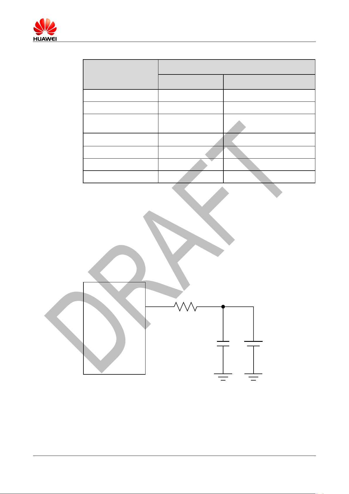
An interrupt is generated if the coin cell voltage drops too low (and the main battery is
not present). If this interrupt occurs, the RTC might be corrupted. A different interrupt
is generated if the crystal oscillator stops; this signifies that handset timing is no
longer accurate. Again, the RTC is corrupted.
When the VBAT power supply of the MC509 is normal, the coin cell charging is
powered from VBAT. The MC509 reads the coin cell voltage and monitors the
charging. During normal operation, the VCOIN pin voltage will stay above 2.2V, even
when the coin cell charger is turned off. Figure 3-2 shows the reference RTC circuit.
Figure 3-2 VCOIN interface circuit
3.3.4 Output Power Supply Interface
Output Power Supply Interface includes VCC_EXT1 PIN, VCC_EXT2 PIN and
UIM_VCC PIN.
Page 26
HUAWEI MC509 CDMA LGA Module
Hardware Guide
Description of the Application Interfaces
Issue 01 (2011-04-08)
Huawei Proprietary and Confidential
Copyright © Huawei Technologies Co., Ltd.
26
Through the Output Power Supply interface, the MC509 module can supply 2.6V and
Pin
No.
Pin Name
I/O
Description
DC Characteristics (V)
Min
Typical
Max
81
POWER_ON_OF
F
I
Pin for controlling
power-on and poweroff
-
Pulled
up on
chip
100
RESIN_N
I
Pin for resetting the
hardware
-0.3
1.8
2.1
91
LED_STATUS
I
Pin for network status
LED
- - -
101
LED_MODE
I
Pin for network mode
LED
- - -
11
WAKEUP_IN
I
H: DTE wakeup
MC509.
L: DTE set MC509 to
sleep mode.
-0.3
2.6
2.9
71
WAKEUP_OUT
O
H: MC509 wakeup
DTE
L: MC509 set DTE to
sleep mode.
-0.3
2.6
2.9
1.8V power externally with an output current of 20mA (typical value) for external level
conversion or other applications.
If the MC509 module is in Sleep mode, the Output Power Supply interface is in the
low power consumption state (< 500μA). If the MC509 module is in Power Down
mode, the Output Power Supply is in the disabled state.
3.4 Signal Control Interface
3.4.1 Overview
The signal control part of the interface in the MC509 module consists of the following:
Power-on/off (POWER_ON_OFF) pin
Hardware reset (RESIN_N) pin
Network status LED (LED_STATUS/LED_MODE) pin
WAKEUP_IN Signal (WAKEUP_IN) pin
WAKEUP_OUT Signal (TBD)
Table 3-5 lists the pins on the signal control interface.
Table 3-5 Pins on the signal control interface
Page 27

HUAWEI MC509 CDMA LGA Module
Hardware Guide
Description of the Application Interfaces
Issue 01 (2011-04-08)
Huawei Proprietary and Confidential
Copyright © Huawei Technologies Co., Ltd.
27
It is recommended that use resistance of 0ohm in the DTE to isolate signals transmitted from
above pins in Table 3-5
3.4.2 Input Signal Control Pins
The MC509 module implements power-on and power-off and resets the hardware
through the input signal control pins.
The power-on, power-off, and reset control parts of the interface of the MC509
module include power-on/power-off interface signal (POWER_ON_OFF) and the
hardware reset interface signal (RESIN_N).
The POWER_ON_OFF pin is used to implement power-on and power-off. If the
POWER_ON_OFF pin is pulled down for at least 0.5s, the module is powered on; if
the POWER_ON_OFF pin is pulled down for at least 2.5s again, the module is
powered off.
The RESET pin is used to reset the hardware. When the software stops responding,
the RESET pin can be pulled down for 100ms to reset the hardware.
As the RESET and POWER_ON_OFF signals are relatively sensitive, it is
recommended that you install a 10nF capacitor near the RESET and
POWER_ON_OFF pins of the interface for filtering. In addition, when you design a
circuit on the PCB of the interface board, it is recommended that the circuit length not
exceed 20mm and that the circuit be kept at a distance of 2.54mm (100mil) at least
from the PCB edge. Furthermore, you need to wrap the area adjacent to the signal
wire with a ground wire. Otherwise, the module may be reset due to interference.
Page 28

HUAWEI MC509 CDMA LGA Module
Hardware Guide
Description of the Application Interfaces
Issue 01 (2011-04-08)
Huawei Proprietary and Confidential
Copyright © Huawei Technologies Co., Ltd.
28
Figure 3-3 shows the connections of the POWER_ON_OFF and RESIN_N pins.
Figure 3-3 Connections of the POWER_ON_OFF and RESIN_N pins
Power-On Time Sequence
After VBAT has been applied and is stable, the module will generate an on board
power on reset signal and on the release of the reset, the module will boot up.
USB_DP will be pulled high when boot up completes, simultaneously the module
starts to communicate with host via USB or UART. Figure 3-4 shows power on timing
sequence.
During power on timing, please make sure the VBAT is stable.
Figure 3-4 Power on timing sequence
Page 29

HUAWEI MC509 CDMA LGA Module
Hardware Guide
Description of the Application Interfaces
Issue 01 (2011-04-08)
Huawei Proprietary and Confidential
Copyright © Huawei Technologies Co., Ltd.
29
Parameter
Comments
Time(Nominal
values)
Units
T
PON
POWER_ON_OFF turn on time.
0.5< T
PON
<1
sec
T
PD+
POWER_ON_OFF Valid to USB
D+ high
4
sec
Parameter
Comments
Time(Nominal values)
Units
T
POFF
POWER_ON_OFF turn off time.
2.5< T
POFF
<4
sec
T
PD+
POWER_ON_OFF Valid to USB
D+ high
4.6
sec
Table 3-6 Power on timing
If the DTE needs to detect the PID/VID of module during the BIOS phase, the
detection time should exceed the T
PD+
time.
Figure 3-5 Power off timing
Table 3-7 Power off timing
Page 30

HUAWEI MC509 CDMA LGA Module
Hardware Guide
Description of the Application Interfaces
Issue 01 (2011-04-08)
Huawei Proprietary and Confidential
Copyright © Huawei Technologies Co., Ltd.
30
For detailed information about power supply design and printed circuit board (PCB) design,
see the HUAWEI LGA Module Power Supply Design Guide and the HUAWEI MC509 CDMA
LGA Module PCB Interconnection Design Guide.
RESIN_N
The MC509 module supports hardware reset function. If the software of the MC509
module stops responding, the MC509 module can be reset through the RESIN_N
signal. After the hardware is reset, the software starts powering on the module and
reports relevant information according to the actual settings. For example, the AT
command automatically reports ^SYSSTART.
3.4.3 Output Signal Control Pin (TBD)
3.4.4 WAKEUP_IN Signal
The DTE controls the sleep and wakeup status of the MC509 module through the
WAKEUP_ IN signal.
If there is no external WAKEUP_IN signal, the wireless module keeps in the wakeup
status by default. After receiving the WAKEUP_ IN signal, the wireless module
determines whether to enter the sleep mode according to the level status of the
WAKEUP_IN signal.
Table 3-5 shows the definition of the WAKE_IN signal.
3.4.5 WAKEUP_OUT Signal
The WAKEUP_OUT signal is used to wake up the external system. Figure 3-6 shows
the recommended schematic.
Page 31

HUAWEI MC509 CDMA LGA Module
Hardware Guide
Description of the Application Interfaces
Issue 01 (2011-04-08)
Huawei Proprietary and Confidential
Copyright © Huawei Technologies Co., Ltd.
31
Figure 3-6 Connections of the WAKEUP_IN and WAKEUP_OUT pins
3.5 UART Interface
3.5.1 Overview
The MC509 module provides the RS-232 UART (9-wire UART) interface for one
asynchronous communication channel. As the UART interface supports signal control
through standard modem handshake, AT commands are entered and serial
communication is performed through the UART interface. The UART has the
following features:
Full-duplex
7-bit or 8-bit data
1-bit or 2-bit stop bit
Odd parity check, even parity check, or non-check
Baud rate clock generated by the system clock
Direct memory access (DMA) transmission
Baud rate ranging from 600 bit/s to 230400 bit/s (115200 bit/s by default)
Self-adapted baud rate ranging from 1200 bit/s to 115200 bit/s
Table 3-8 lists the UART interface signals.
Page 32

HUAWEI MC509 CDMA LGA Module
Hardware Guide
Description of the Application Interfaces
Issue 01 (2011-04-08)
Huawei Proprietary and Confidential
Copyright © Huawei Technologies Co., Ltd.
32
Table 3-8 UART interface signals
Pin
No.
Pin Name
I/O
Description
Feature
DC Characteristics (V)
Min
Typical
Max
76
UART_TX
O
Data sending on the
wireless module
The DTE receives
serial data.
-0.3
2.6
2.9
78
UART_RX
I
Data receive end of
the module
The DTE transmits
serial data.
-0.3
2.6
2.9
77
UART_RIN
G
O
Ringing indication on
the wireless module
The DTE is notified of
a remote call.
-0.3
2.6
2.9
74
UART_RTS
O
Data sending request
on the wireless
module
The DTE notifies the
DCE of sending
requests.
-0.3
2.6
2.9
79
UART_DTR
I
Data terminal ready
on the wireless
module
The DTE is ready.
-0.3
2.6
2.9
80
UART_CTS
I
Clearing to send on
the wireless module
The DCE switches to
the receiving mode.
-0.3
2.6
2.9
75
UART_DCD
O
Data carrier
detection on the
wireless module
Data links are
connected.
-0.3
2.6
2.9
73
UART_DSR
O
Data ready on the
wireless module
The DCE is ready.
-0.3
2.6
2.9
3.5.2 Circuit Recommended for the UART Interface
Figure 3-7 shows the connection of the UART interface in the MC509 module (DCE)
with the host (DTE).
Page 33

HUAWEI MC509 CDMA LGA Module
Hardware Guide
Description of the Application Interfaces
Issue 01 (2011-04-08)
Huawei Proprietary and Confidential
Copyright © Huawei Technologies Co., Ltd.
33
Figure 3-7 Connection of the UART interface in the MC509 module (DCE) with the host
Pin No.
Pin Name
I/O
Description
86
USB_DP
I/O
USB data signal D+
85
USB_DM
I/O
USB data signal D-
(DTE)
The RS-232 Transceivers can be used to connect the MC509 module to the RS-232C interface. In this connection, the complementary metal oxide semiconductor
(COMS) level and the Electronic Industries Association (EIA) level are converted
mutually.
For detailed application of the MC509 UART interface, see the HUAWEI LGA Module UART
Design Guide.
It is recommended that set the pins related to UART interface as test points on the DTE for
debug.
3.6 USB Interface
The MC509 is compliant with USB 2.0 full speed protocol. The USB interface is
powered directly from the 3.3 V supply. The USB input/output lines are compatible
with the USB 2.0 3.3 V signal specifications. 0shows the circuit of the USB interface.
Table 3-9 USB interface signals
Page 34

HUAWEI MC509 CDMA LGA Module
Hardware Guide
Description of the Application Interfaces
Issue 01 (2011-04-08)
Huawei Proprietary and Confidential
Copyright © Huawei Technologies Co., Ltd.
34
VOHmin
VOLmax
VIHmin
VILmax
2.8V
0.3V
2V
0.8V
The USB interface is powered directly from the 3.3 V supply. The USB input/output lines are
compatible with the USB 2.0 3.3 V signal specifications.
Table 3-10 DC Electrical Characteristics of USB
Figure 3-8 Recommended circuit of USB interface
Since the USB interface of MC509 module supports USB 2.0 full speed, the resistance
“RV102 and RV103” in the 0must be Voltage Sensitive Resistor with small capacitance
(ALVC18S02003 manufactured by AMOTECH or B72590T7900V60 manufactured by
EPCOS is recommended.). In addition, The layout design of this circuit on the DTE board
should comply with the USB 2.0 full speed protocol, with differential lining and impedance
control to 90 ohm
It is recommended that set USB D+ and USB D- pins as test points and then place these
test points on the DTE for debug.
Page 35
HUAWEI MC509 CDMA LGA Module
Hardware Guide
Description of the Application Interfaces
Issue 01 (2011-04-08)
Huawei Proprietary and Confidential
Copyright © Huawei Technologies Co., Ltd.
35
3.7 UIM Card Interface
Pin No.
Pin Name
I/O
Description
DC Characteristics (V)
Min
Typical
Max
34
UIM_VCC
O
Power source for the
external UIM.
-0.3
1.8/2.85
2.1/3.15
89
UIM_DATA
I/O
External UIM data
signal.
-0.3
1.8/2.85
2.1/3.15
90
UIM_CLK
O
External UIM clock
signal.
-0.3
1.8/2.85
2.1/3.15
88
UIM_RESET
O
External UIM reset
signal.
-0.3
1.8/2.85
2.1/3.15
3.7.1 Overview
The MC509 module provides a UIM card interface complying with the ISO 7816-3
standard and supports automatic detection of a 3.0V UIM card or a 1.8V UIM card.
Table 3-11 lists the UIM card interface signals.
Table 3-11 UIM card interface signals
3.7.2 Circuit Recommended for the UIM Card Interface
As the MC509 module is not equipped with a UIM card socket, a UIM card socket
need to be placed on the user interface board. The UIM card signals are transmitted
outwards through the 145-pin LGA interface. Figure 3-9 shows the circuit of the UIM
card interface.
Page 36
HUAWEI MC509 CDMA LGA Module
Hardware Guide
Description of the Application Interfaces
Issue 01 (2011-04-08)
Huawei Proprietary and Confidential
Copyright © Huawei Technologies Co., Ltd.
36
Figure 3-9 Circuit of the UIM card interface
pin1:
UIM_PWR
pin2:
UIM_RESET
pin3:
UIM_CLK
pin4:
GND
pin5:
NULL
pin6:
UIM_DATA
Figure 3-10 Pin definition of UIM Socket
Page 37
HUAWEI MC509 CDMA LGA Module
Hardware Guide
Description of the Application Interfaces
Issue 01 (2011-04-08)
Huawei Proprietary and Confidential
Copyright © Huawei Technologies Co., Ltd.
37
To meet the requirements of ETSI TS 102 230protocols and electromagnetic
compatibility (EMC) authentication, the UIM card socket should be placed near the
LGA interface (it is recommended that the PCB circuit connecting the LGA
interface and the UIM card socket not exceed 100mm), because a long circuit
may lead to wave distortion, thus affecting signal quality.
It is recommended that the user should wrap the area adjacent to the UIM_CLK
and UIM_DATA signal wires with a ground wire. The GND pin of the UIM card
socket and the GND pin of the UIM card must be well connected to the power
GND pin supplying power to the MC509 module.
A 0.1μF capacitor is placed between the UIM_VCC and GND pins in a parallel
manner. Three 10pF or 33pF capacitors are placed between the UIM_DATA and
GND pins, the UIM_RST and GND pins, and the UIM_CLK and GND pins in
parallel to filter interference from RF signals.
It is not recommended that pull the UIM_DATA pin up during design as a 15000ohm resistor is used to connect the UIM_DATA pin to the UIM_VCC.
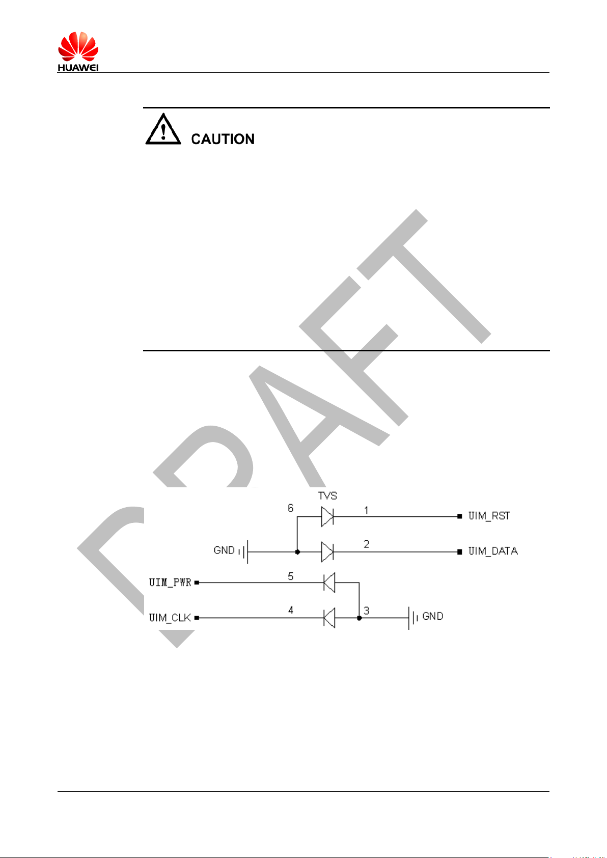
3.7.3 ESD Protection for the UIM Card Interface
It is recommended to take electrostatic discharge (ESD) protection measures near
the UIM card socket. Figure 3-11 shows ESD protection circuit of the UIM card, in
which the transient voltage suppressor (TVS) diode is placed as close as possible to
the UIM card socket, and the GND pin of the ESD protection component is well
connected to the power GND pin that supplies power to the MC509 module.
Figure 3-11 ESD protection circuit on the UIM card
3.8 Audio Interface
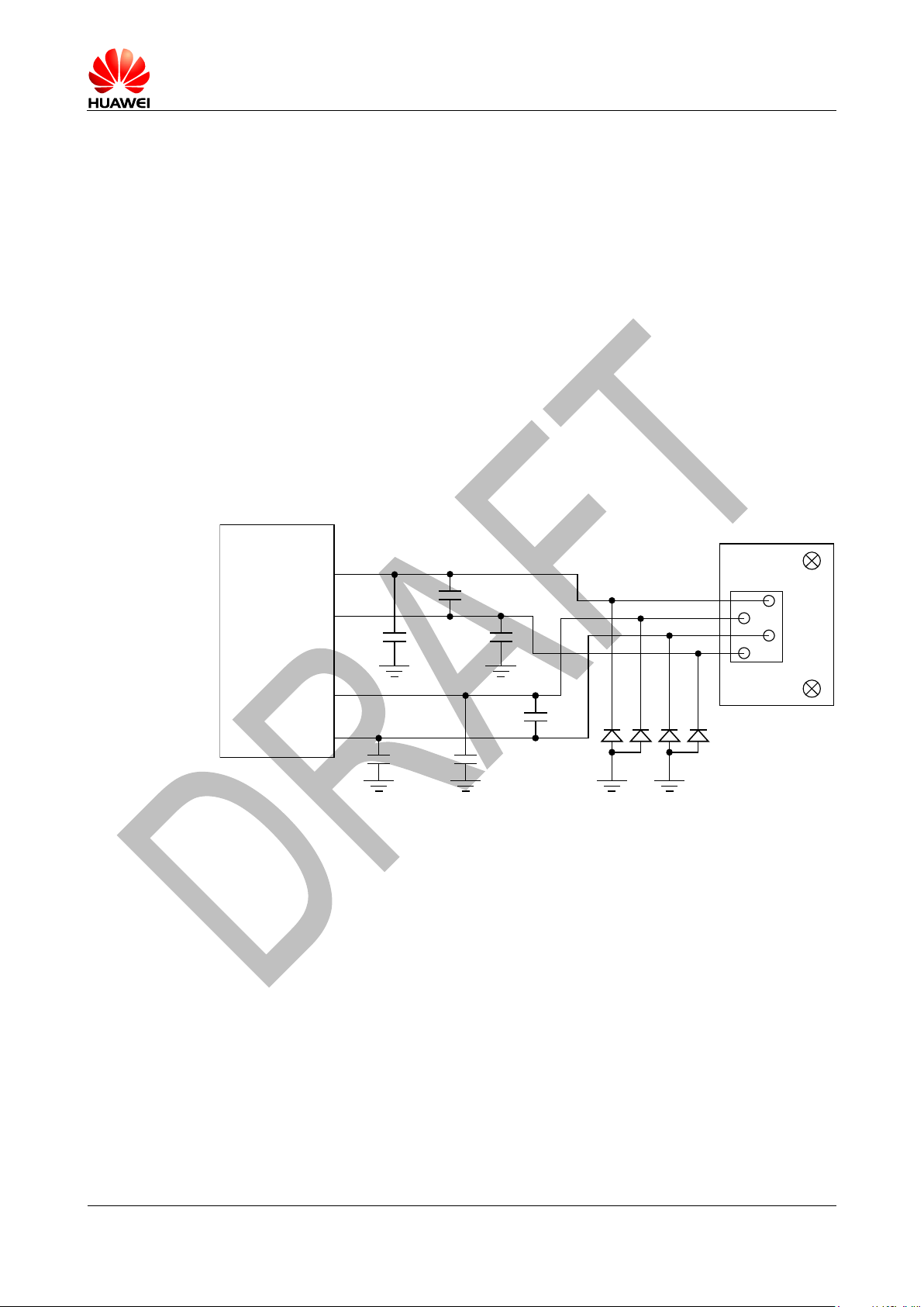
3.8.1 Analogue Audio
The MC509 provides two audio I/O channels (Data only doesn’t support the voice
function).
Page 38
HUAWEI MC509 CDMA LGA Module
Hardware Guide
Description of the Application Interfaces
Issue 01 (2011-04-08)
Huawei Proprietary and Confidential
Copyright © Huawei Technologies Co., Ltd.
38
The two audio I/O channels are completely different and thus have good performance
Module
(DCE)
MIC1_P
MIC1_N
EAR_OUT_P
EAR_OUT_N
1nF
1nF
1nF
1nF
1nF1nF
ESD protection
Network
Connector
of resisting RF interferences. The routes on the printed circuit board (PCB) should be
placed in parallel with each other and should be short. The filter circuit on the two
sides should be symmetric. The differential signals should be close to each other.
The audio output signals in differential pairs and the audio input signals in differential
pairs should be separated effectively through ground. In addition, the audio signals
should be located away from the circuits of the power supply, RF, and antenna.
The first audio channel can be used for the handset without requiring any audio
amplifier. The output power for the differential ear output is typically 350mW for a fullscale +3dBm sine wave into a 32-ohm speaker.
The second audio channel can be used for the hands-free without requiring any
audio amplifier. The output pins are configured differently, with a rated output of 500
mW into an 8Ω speaker. Considerable current flows between the audio output pins
and the speaker, and thus wide PCB traces are recommended (20mils).
MC509 provides 2.2V power source and 1mA of bias current internally for the
microphones of both audio channels.
Figure 3-12 Circuit diagram of the interface of the first audio channel
Page 39

HUAWEI MC509 CDMA LGA Module
Hardware Guide
Description of the Application Interfaces
Issue 01 (2011-04-08)
Huawei Proprietary and Confidential
Copyright © Huawei Technologies Co., Ltd.
39
Figure 3-13 Circuit diagram of the interface of the second audio channel
Module
(DCE)
+
_
ESD protection
ESD protection
ferrite bead
SPKR_OUT_P
SPKR_OUT_N
MIC2_P
MIC2_N
ferrite bead
ferrite bead
ferrite bead
1nF
1nF 1nF
1nF
1nF1nF
Speaker
MIC
+
_
Pin
No.
Pin Name
I/O
Description
DC Characteristics (V)
Min
Typical
Max
5
PCM_SYNC
O
PCM interface sync
-0.3
2.6
2.9
6
PCM_DIN
I
PCM I/F data in
-0.3
2.6
2.9
7
PCM_DOU
T
O
PCM I/F data out
-0.3
2.6
2.9
8
PCM_CLK
O
PCM interface clock
-0.3
2.6
2.9
3.8.2 Digital Audio
It is recommended that a TVS be used on the related interface, to prevent electrostatic
discharge and protect integrated circuit (IC) components.
Data only does not support the voice function.
The MC509 provides one digital audio channels (Data only doesn’t support the voice
function). Table 3-12 lists the signals on the digital audio interface.
Table 3-12 Signals on the digital audio interface
The MC509 PCM interface enables communication with an external codec to support
linear and μ-law format. The PCM_SYNC runs at 8kHz with a 50% duty cycle.
Page 40

HUAWEI MC509 CDMA LGA Module
Hardware Guide
Description of the Application Interfaces
Issue 01 (2011-04-08)
Huawei Proprietary and Confidential
Copyright © Huawei Technologies Co., Ltd.
40
Figure 3-14 Circuit diagram of the interface of the PCM (MC509 is used as PCM master)
Pin No.
Pin
Name
I/O
Description
DC Characteristics (V)
Min
Type
Max
44,46,51,55,
105,109,113,
GPIO
I/O
General I/O
pins
-0.3
2.6
2.9
PCM_SYNC: Output when PCM master
PCM_CLK: Output when PCM master
It is recommended that a TVS be used on the related interface, to prevent electrostatic
discharge and protect integrated circuit (IC) components.
Data only edition does not support the voice function.
Primary Mode
On Primary mode MU509 provides a 16-bit linear or μ-law, with short-sync and
2.048MHz clock (on the PCM_CLOCK pin).
3.9 General Purpose I/O Interface
The LGA module provides seven channels GPIO pins for customers to applications of
controlling signal. Customers can use AT command to control the state of logic levels
of eight channels GPIO output signal. See the HUAWEI MC509 CDMA LGA Module
AT Command Interface Specification.
Page 41

HUAWEI MC509 CDMA LGA Module
Hardware Guide
Description of the Application Interfaces
Issue 01 (2011-04-08)
Huawei Proprietary and Confidential
Copyright © Huawei Technologies Co., Ltd.
41
3.10 JTAG Interface
Pin No.
Pin Name
I/O
Description
DC Characteristics (V)
Min
Type
Max
31
VCC_EXT2
O
2.6V POWER
output
-
2.6
-
100
RESIN_N
I
Reset module
-0.3
1.8
2.1
30
JTAG_TMS
I
JTAG Test
mode select
-0.3
2.6
2.9
36
JTAG_TRST_N
I
-0.3
2.6
2.9
42
JTAG_TCK
I
JTAG clock
input
-0.3
2.6
2.9
72
JTAG_TDO
Z
JTAG test data
output
-0.3
2.6
2.9
87
JTAG_TDI
I
JTAG test data
input
-0.3
2.6
2.9
93
JTAG_RTCK
O
JTAG return
clock
-0.3
2.6
2.9
14
PS_HOLD
This input high
to keep power
on, low to
shut down.
-
1.8
LGA MC509 module provides one JTAG interface (Joint Test Action Group). Set the
pins in the following table as the test pins. And place the test points in the DTE for
debug.
It is recommended that set the 9 pins related to JTAG interface as test points on the DTE for
tracing and debug.
3.11 RF Antenna Interface
MC509 module provides an RF ANT PAD for connecting an external antenna.
Through the MAIN_ANT pad, the antenna interface is routed to the coaxial connector
on the DTE (Impedance 50).The external antenna is connected to the module
through the coaxial connector.
A matching location for the antenna must be reserved at the antenna port.
Page 42

HUAWEI MC509 CDMA LGA Module
Hardware Guide
Description of the Application Interfaces
Issue 01 (2011-04-08)
Huawei Proprietary and Confidential
Copyright © Huawei Technologies Co., Ltd.
42
Table 3-13 Signals on RF Antenna interface
Pin No.
Pin Name
I/O
Description
DC Characteristics (V)
Min
Typical
Max
107
MAIN_ANT
-
RF main
antenna
interface
- - -
111
GPS_ANT
-
RF GPS
antenna
interface
- - -
115
AUX_ANT
RF divert
antenna
interface
- - -
Pin No.
Pin
Name
I/O
Description
DC Characteristics (V)
Min
Typical
Max
1~4,9,10,16~27,33, 37,
47,60~70,82~84,92,94,
95, 102~104.117~120
NC
-
Not
connected,
please keep
this pin
open
- - -
3.12 NC Pins
The LGA module has 45 NC pins. All the NC interfaces should not be connected.
Please keep this pin open.
Page 43

错误!未知的文档属性名称
Hardware Guide
RF Specifications
Issue 01 (2011-04-08)
Huawei Proprietary and Confidential
Copyright © Huawei Technologies Co., Ltd.
43
4.1 About This Chapter
Operating Band
Tx
Rx
CDMA 800 (BC0)
824MHz ~ 849MHz
869MHz ~ 894MHz
CDMA 1900 (BC1)
1850MHz ~ 1910MHz
1930MHz ~ 1990MHz
This chapter describes the RF specifications of the MC509 module, including:
Antenna Installation Guidelines
Operating Frequencies
Conducted RF Measurement
Conducted Rx Sensitivity and Tx Power
Antenna Design Requirements
4 RF Specifications
4.2 Antenna Installation Guidelines
Install the antenna in a place covered by the signal.
The Antenna must be installed to provide a separation distance of at least 20 cm
from all persons and must not be co-located or operating in conjunction with any
other antenna or transmitter.
Antenna must not be installed inside metal cases.
Antenna must be installed also according Antenna manufacturer instructions.
4.3 Operating Frequencies
错误!未找到引用源。 shows the RF bands supported by MC509 RF bands
Page 44

错误!未知的文档属性名称
Hardware Guide
RF Specifications
Issue 01 (2011-04-08)
Huawei Proprietary and Confidential
Copyright © Huawei Technologies Co., Ltd.
44
4.4 Conducted RF Measurement
Test instrument
Agilent 8960
Power supply
KEITHLEY 2306
RF cable for testing
L08-C014-350 of DRAKA COMTEQ or Rosenberger
Cable length: 29cm
Compensation for CDMA 850MHz:0.8dB
Compensation for CDMA 2100MHz:1dB
Item
3GPP2
Protocol
Claim (dBm)
MC509 Test Value (dBm)
Min
Typical
Max
CDMA 800
1x(FER<0.5%)
< -104
- -104
EVDO(FER<0.5%)
< -105.5
- -105.5
CDMA1900
1x(FER<0.5%)
< -104
- -104
EVDO(FER<0.5%)
< -105.5
- -105.5
4.4.1 Test Environment
The compensation for different frequency bands relates to the cable and the test
environment.
The instrument compensation needs to be set according to the actual cable conditions.
4.4.2 Test Standards
Huawei modules meet all 3GPP2 test standards relating to 3G. Each module passes
strict tests at the factory and thus the quality of the modules is guaranteed.
4.5 Conducted Rx Sensitivity and Tx Power
4.5.1 Conducted Receive Sensitivity
The conducted receive sensitivity is a key parameter that indicates the receiver
performance of MC509. The conducted receive sensitivity refers to the weakest
signal that the module at the antenna port can receive. The BER must meet the
3GPP protocol requirements in the case of the minimum signal.
The 3GPP Protocol Claim column in Table 4-1 lists the required minimum values,
and the Test Value column lists the tested values of MC509.
Table 4-1 MC509 conducted Rx sensitivity (Unit: dBm)
Page 45

错误!未知的文档属性名称
Hardware Guide
RF Specifications
Issue 01 (2011-04-08)
Huawei Proprietary and Confidential
Copyright © Huawei Technologies Co., Ltd.
45
Item
MC509 Test Value (dBm)
Min
Typical
Max
BC0(CDMA 800MHz)
23
24
26
BC1(CDMA 1900MHz)
23
24
26
The test values are the average of some test samples.
4.5.2 Conducted Transmit Power
The conducted transmit power is another indicator that measures the performance of
MC509. The conducted transmit power refers to the maximum power that the module
tested at the antenna port can transmit. According to the 3GPP2 protocol, the
required transmit power varies with the power class.
Table 4-2 lists the required ranges of the conducted transmit power of MC509. The
tested values listed in the Test Value column must range from the minimum power to
the maximum power.
Table 4-2 MC509 conducted Tx power (Unit: dBm)
4.6 Antenna Design Requirements
4.6.1 Antenna Design Indicators
Antenna Efficiency
Antenna efficiency is the ratio of the input power to the radiated or received power of
an antenna. The radiated power of an antenna is always lower than the input power
due to the following antenna losses: return loss, material loss, and coupling loss. The
efficiency of an antenna relates to its electrical dimensions. To be specific, the
antenna efficiency increases with the electrical dimensions. In addition, the
transmission cable from the antenna port of MC509 to the antenna is also part of the
antenna. The cable loss increases with the cable length and the frequency. It is
recommended that the cable loss be as low as possible, for example, U.FL-LP-088
made by HRS.
The following antenna efficiency (free space) is recommended for MC509 to ensure
high radio performance of the module: Efficiency of the master antenna > 50% (–
4dB), In addition, the efficiency should be tested with the transmission cable.
S11 or VSWR
S11 (return loss) indicates the degree to which the input impedance of an antenna
matches the reference impedance (50-ohm). S11 shows the resonance feature and
impedance bandwidth of an antenna. Voltage standing wave ratio (VSWR) is another
Page 46

错误!未知的文档属性名称
Hardware Guide
RF Specifications
Issue 01 (2011-04-08)
Huawei Proprietary and Confidential
Copyright © Huawei Technologies Co., Ltd.
46
expression of S11. S11 relates to the antenna efficiency. S11 can be measured with a
vector analyzer.
The following S11 values are recommended for the antenna of MC509: S11 of the
master antenna < –6dB
Polarization
The polarization of an antenna is the orientation of the electric field vector that rotates
with time in the direction of maximum radiation.
The linear polarization is recommended for the antenna of MC509.
Radiation Pattern
The radiation pattern of an antenna reflects the radiation features of the antenna in
the remote field region. The radiation pattern of an antenna commonly describes the
power or field strength of the radiated electromagnetic waves in various directions
from the antenna. The power or field strength varies with the angular coordinates (θ
and φ), but is independent of the radial coordinates.
The radiation pattern of half wave dipole antennas can be used for wireless terminals.
The radiation pattern of half wave dipole antennas is omnidirectional in the horizontal
plane, and the incident waves of base stations are often in the horizontal plane. For
this reason, the receiving performance is optimal.
The following radiation patterns are recommended for the antenna of MC509: Master
antenna: omnidirectional
Gain and Directivity
The radiation pattern of an antenna represents the field strength of the radiated
electromagnetic waves in all directions, but not the power density that the antenna
radiates in the specific direction. The directivity of an antenna, however, measures
the power density that the antenna radiates.
Gain, as another important parameter of antennas, correlates closely to the directivity.
The gain of an antenna takes both the directivity and the efficiency of the antenna
into account. The appropriate antenna gain prolongs the service life of relevant
batteries.
The following antenna gain is recommended for MC509: Gain of the master
antenna ≤ 2.5dBi
The antenna consists of the antenna body and the relevant RF transmission cable. Take
the RF transmission cable into account when measuring any of the preceding antenna
indicators.
Huawei cooperates with various famous antenna suppliers who are able to make
suggestions on antenna design, for example, Amphenol, Skycross, Pulse, etc.
Page 47

错误!未知的文档属性名称
Hardware Guide
RF Specifications
Issue 01 (2011-04-08)
Huawei Proprietary and Confidential
Copyright © Huawei Technologies Co., Ltd.
47
4.6.2 Interference
CDMA Antenna Requirements
Frequency range
Depending on frequency band (s)provided by the network
operator, the customer must use the most suitable
antenna for that/those band (s)
Bandwidth
80MHz in CDMA800
140MHz in CDMA1900
Gain
Gain < 3dBi
Impedance
50-ohm
Input power
> 24dBm Average power in CDMA
VSWR absolute max
<= 10:1
VSWR recommended
<= 2:1
Besides the antenna performance, the interference on the user board also affects the
radio performance (especially the TIS) of the module. To guarantee high performance
of the module, the interference sources on the user board must be properly controlled.
On the user board, there are various interference sources, such as the LCD, CPU,
audio circuits, and power supply. All the interference sources emit interference
signals that affect the normal operation of the module. For example, the module
sensitivity can be decreased due to interference signals. Therefore, during the design,
you need to consider how to reduce the effects of interference sources on the module.
You can take the following measures: Use an LCD with optimized performance;
shield the LCD interference signals; shield the signal cable of the board; or design
filter circuits.
Huawei is able to make technical suggestions on radio performance improvement of
the module.
4.6.3 CDMA Antenna Requirements
The antenna for MC509 must fulfill the following requirements:
Furthermore if the device is developed for the US and/or Canada market, it must
comply with the FCC and/or IC requirements:
This device is to be used only for mobile and fixed application. The antenna(s) used
for this transmitter must be installed to provide a separation distance of at least 20cm
from all persons and must not be co-located or operating in conjunction with any
other antenna or transmitter. End-users must be provided with transmitter operation
conditions for satisfying RF exposure compliance. OEM integrators must ensure that
the end user has no manual instructions to remove or install the UC864-E/G/WD
/WDU module. Antennas used for this OEM module must not exceed 3dBi gain for
mobile and fixed operating configurations.
Page 48

错误!未知的文档属性名称
Hardware Guide
RF Specifications
Issue 01 (2011-04-08)
Huawei Proprietary and Confidential
Copyright © Huawei Technologies Co., Ltd.
48
4.6.4 Radio Test Environment
The antenna efficiency, antenna gain, radiation pattern, total radiated power (TRP),
and TIS can be tested in a microwave testing chamber.
Huawei has a complete set of OTA test environments (SATIMO microwave testing
chambers and ETS microwave testing chambers). The testing chambers are certified
by professional organizations and are applicable to testing at frequencies ranging
from 380MHz to 6GHz. The test items are described as follows:
Passive Tests
Antenna efficiency
Gain
Pattern shape
Envelope correlation coefficient
Active Tests
TRP: GSM, WCDMA, CDMA, TD-SCDMA, and LTE systems
TIS: GSM, WCDMA, CDMA, TD-SCDMA, and LTE systems
Figure 4-1 shows the SATIMO microwave testing chamber.
Figure 4-1 SATIMO microwave testing chamber
Page 49
错误!未知的文档属性名称
Hardware Guide
Electrical and Reliability Features
Issue 01 (2011-04-08)
Huawei Proprietary and Confidential
Copyright © Huawei Technologies Co., Ltd.
49
5 Electrical and Reliability Features
Symbol
Specification
Minimum
Value
Maximum
Value
Unit
VBAT
External power voltage
-0.5
5.0
V
VCOIN
Input voltage of standby
power for the RTC
1.5
3.15
V
VI
Data pin voltage
-0.4
3.3
V
5.1 About This Chapter
This chapter describes the electrical and reliability features of the interfaces in the
MC509 module, including:
Extreme Working Conditions
Working and Storage Temperatures and Humidity
Power Supply Features
Reliability Features
EMC and ESD Features
5.2 Extreme Working Conditions
Table 5-1 lists the extreme working conditions for the MC509 module. Using the
MC509 module beyond these conditions may result in permanent damage to the
module.
Table 5-1 Extreme working conditions for the MC509 module
Page 50

错误!未知的文档属性名称
Hardware Guide
Electrical and Reliability Features
Issue 01 (2011-04-08)
Huawei Proprietary and Confidential
Copyright © Huawei Technologies Co., Ltd.
50
5.3 Working and Storage Temperatures and Humidity
Specification
Minimum Value
Maximum Value
Unit
Normal working
temperatures [1]
TBD
TBD
°C
Extreme working
temperatures [2]
TBD
TBD
°C
Ambient temperature for
storage
TBD
TBD
°C
Moisture
TBD
TBD
%
Parameter
Description
Minimum Value
Maximum Value
Unit
VIH
High-level input
voltage
0.65*VDD_PX
VDD_PX + 0.3
V
VIL
Low-level input
voltage
-0.3
0.35* VDD_PX
V
I
leak
Input leakage
current
-0.2
0.2
μA
VOH
High-level
output voltage
VDD_PX – 0.45
VDD_PX
V
VOL
Low-level output
voltage
0
0.45
V
IOH
High-level
output current
1.5 mA
Table 5-2 lists the working and storage temperatures and humidity for the MC509
module.
Table 5-2 Working and storage temperatures and humidity for the MC509 module
[1]: When the MC509 module works at this temperature, all its RF indexes comply with the
3GPP2 C.S057D specifications.
[2]: When the MC509 module works at this temperature, certain RF indexes do not comply with
the 3GPP2 C.S057D specifications.
5.4 Electrical Features of Application Interfaces
Table 5-3 lists electrical features (typical values).
Table 5-3 Electrical features of application interfaces
Page 51
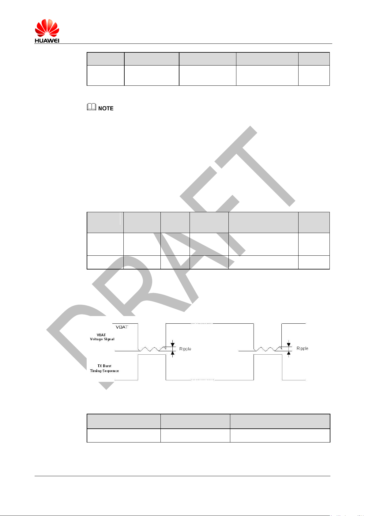
错误!未知的文档属性名称
Hardware Guide
Electrical and Reliability Features
Issue 01 (2011-04-08)
Huawei Proprietary and Confidential
Copyright © Huawei Technologies Co., Ltd.
51
Parameter
Description
Minimum Value
Maximum Value
Unit
IOL
Low-level output
current
-1.5
mA
Parameter
Minimum
Value
Typical
Value
Maximum
Value
Ripple
Unit
VBAT
3.0
3.8
4.2
< 50mVpp
(0Hz to 2.5GHz)
V
VCOIN
1.5
3.0
3.25
< 30mVpp
V
Power
Peak (Maximum)
Normal (Maximum)
3.8V
<1500mA
<1000mA
VDD_PX is 2.6V or 1.8V, about the voltage, please refer to Table 3-1 .
5.5 Power Supply Features
5.5.1 Input Power Supply
Table 5-4 lists the requirements for input power of the MC509 module.
Table 5-4 Requirements for input power of the MC509 module
Figure 5-1 lists the Power Supply During Burst Emission
Figure 5-1 Power Supply During Burst Emission
Table 5-5 Requirements for input current of the MC509 module
Page 52

错误!未知的文档属性名称
Hardware Guide
Electrical and Reliability Features
Issue 01 (2011-04-08)
Huawei Proprietary and Confidential
Copyright © Huawei Technologies Co., Ltd.
52
5.5.2 Power Consumption
Working mode
Max
Unit
Power off mode
TBD
μA
Standby mode
800M
TBD
mA
1900M
TBD
mA
Data mode
800M
TBD
mA
1900M
TBD
mA
Item
Test Condition
Standard
Low-temperature
storage
Temperature: –40±2 ºC
Test duration: 24h
IEC60068
High-temperature
storage
Temperature: 85±2 ºC
Test duration: 24h
IEC60068
Low-temperature
working
Temperature: –30±2 ºC
Test duration: 24h
IEC60068
High-temperature
working
Temperature: 75±2 ºC
Test duration: 24h
IEC60068
The power consumptions of MC509 in different scenarios are respectively listed in
Table 5-6 .
The power consumption listed in this section is tested when the power supply of
MC509 module is 3.8V. Typical values are measured at room temperature, and
minimum and maximum values are measured over the entire operating temperature
range.
Table 5-6 Averaged standby DC power consumption
Standby current consumption with Sleep mode deactivated-Idle(assumes USB bus is fully
suspended during measurements)
The above values are the average of some test samples.
5.6 Reliability Features
Table 5-7 lists the test conditions and results of the mechanical reliability of the
MC509 module.
Table 5-7 Test conditions and results of the mechanical reliability of the MC509 module
Page 53
错误!未知的文档属性名称
Hardware Guide
Electrical and Reliability Features
Issue 01 (2011-04-08)
Huawei Proprietary and Confidential
Copyright © Huawei Technologies Co., Ltd.
53
Item
Test Condition
Standard
Damp heat cycling
High temperature: 55±2 ºC
Low temperature: 25±2 ºC
Humidity: 95%
Repetition times: 4
Test duration: 12h + 12h
IEC60068
Temperature shock
Low temperature: –40±2 ºC
High temperature: 85±2 ºC
Temperature change interval: < 30s
Test duration: 15min
Repetition times: 100
IEC60068
Salty fog test
Temperature: 35°C
Density of the NaCl solution: 5±1 %
Spraying interval: 8h
Duration of exposing the module to
the temperature of 35°C: 16h
IEC60068
Sine vibration
Frequency range: 5Hz to 200Hz
Acceleration: 10m/s2
Frequency scan rate: 1oct/min
Test period: 3 axial directions. Five
circles for each axial direction.
IEC60068
Shock test
Half-sine wave shock
Peak acceleration: 300m/s2
Shock duration: 11ms
Test period: 6 axial directions. One
shock for each axial direction.
IEC60068
Clash test
Half-sine wave
Peak acceleration: 180m/s2
Pulse duration: 6ms
Repetition time: 6 directions. 1000
times for each direction.
IEC60068
Drop test
First case: 0.3m in height. Drop the
MC509 module on the marble
terrace with one surface facing
downwards twice. Six surfaces
should be tested.
Second case: 0.8m in height. Drop
the MC509 module on the marble
terrace with one surface facing
downwards twice. Six surfaces
should be tested.
IEC60068
Page 54
错误!未知的文档属性名称
Hardware Guide
Electrical and Reliability Features
Issue 01 (2011-04-08)
Huawei Proprietary and Confidential
Copyright © Huawei Technologies Co., Ltd.
54
5.7 EMC and ESD Features
EMC tests have to be performed on the application as soon as possible to detect any
potential problems.
When designing, special attention should be paid to the following:
Possible harmful emissions radiated by the application to the RF receiver in the
receiver band.
ESD protection is mandatory on all signals which are externally accessible
Typically, ESD protection is mandatory for the following:
− UIM (if accessible from outside)
− Serial link
− USB
− Audio
Length of the UIM interface lines (preferably <10cm).
EMC protection on audio input/output (filters against 900MHz emissions).
Biasing of the microphone inputs.
Ground plane: HUAWEI Wireless recommends a common ground plane for
analog/digital/RF grounds.
A metallic case or plastic casing with conductive paint is recommended, except
for the area around the antenna.
The HUAWEI MC509 Module does not include any protection against over voltage.
Page 55

错误!未知的文档属性名称
Hardware Guide
Mechanical Specifications
Issue 01 (2011-04-08)
Huawei Proprietary and Confidential
Copyright © Huawei Technologies Co., Ltd.
55
6 Mechanical Specifications
6.1 About This Chapter
This chapter describes the following aspects of the MC509 module:
Dimensions and interfaces
PCB Pad Design
Label
Packing System
6.2 Dimensions and interfaces
The dimension of MC509 is 30mm (length) × 30mm (width) × 2.6mm (height).
Figure 6-1 shows the dimensions of MC509 in details.
Figure 6-1 Dimensions of MC509
Page 56
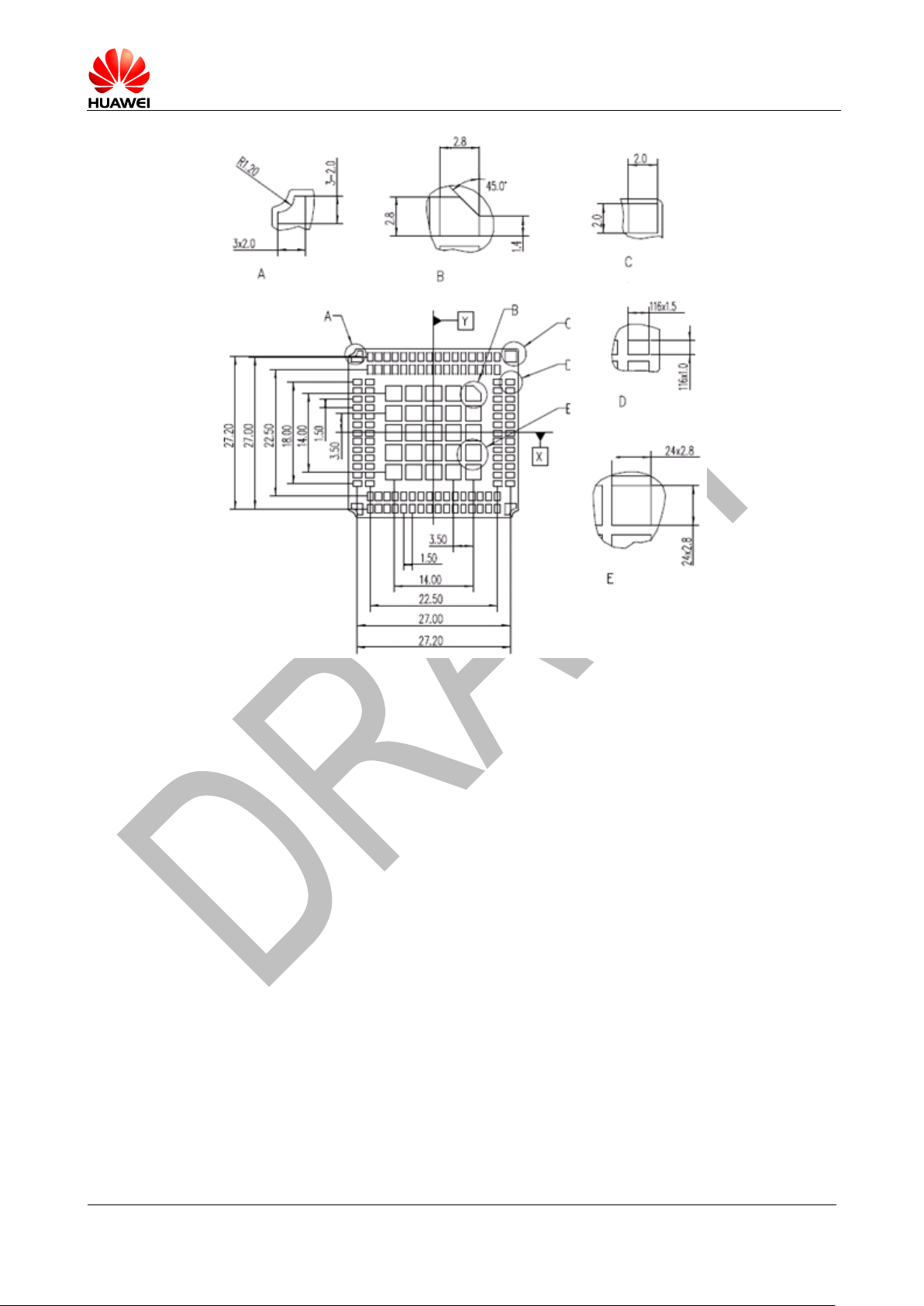
错误!未知的文档属性名称
Hardware Guide
Mechanical Specifications
Issue 01 (2011-04-08)
Huawei Proprietary and Confidential
Copyright © Huawei Technologies Co., Ltd.
56
6.3 PCB Pad Design
To achieve assembly yields and solder joints of high reliability, it is recommended that
the PCB pad size be designed as follows: the size of the pad in the middle region is
the same as the pad size of the product package; other pads are 0.05 mm larger than
the unilateral pad of the product package. For details, see Figure 6-2 .
Page 57
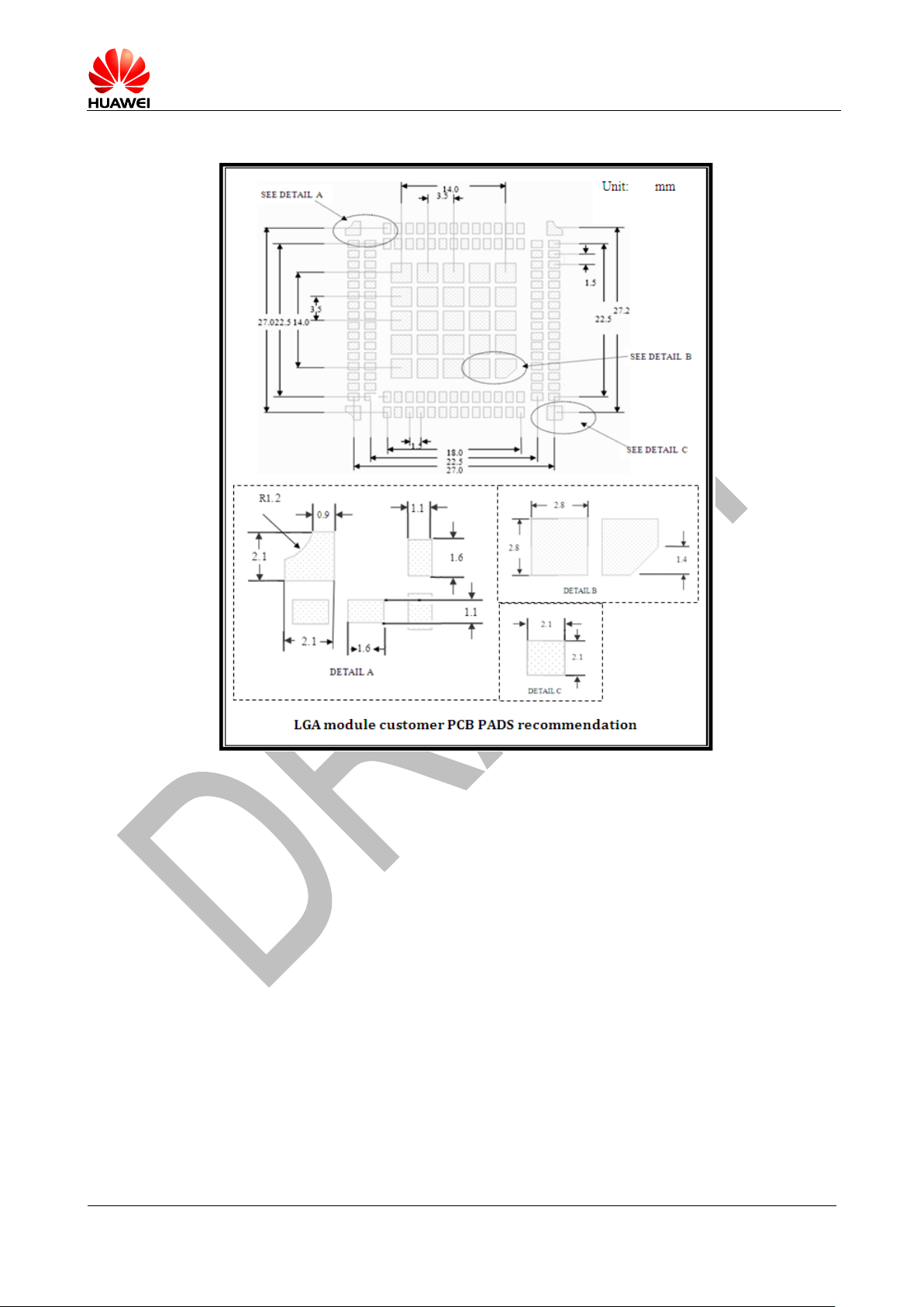
错误!未知的文档属性名称
Hardware Guide
Mechanical Specifications
Issue 01 (2011-04-08)
Huawei Proprietary and Confidential
Copyright © Huawei Technologies Co., Ltd.
57
Figure 6-2 PCB pad design
6.4 Label
The label is made from deformation-resistant, fade-resistant, and high-temperatureresistant material and is able to endure the high temperature of 260°C .
Page 58

错误!未知的文档属性名称
Hardware Guide
Mechanical Specifications
Issue 01 (2011-04-08)
Huawei Proprietary and Confidential
Copyright © Huawei Technologies Co., Ltd.
58
Figure 6-3 Nameplate
The picture mentioned above is only for reference.
Make the film according to the drawing.
The silk-screen should be clear, without burrs, and dimension should be accurate.
This nameplate should not be covered by the film.
The material and surface finishing and coatings which used have to make satisfied with the
EU WEEE and RoHS directives.
The label must be heated up for 20s~40s and able to endure the high temperature of
260 °C . And the color of the material of the nameplate can’t change.
6.5 Packing System
HUAWEI LGA module uses five layers ESD pallet, anti-vibration foam and vacuum
packing into cartons. To get the details about the packing system, please refer to
HUAWEI LGA Module Technical Guide for Assembly.
Page 59

HUAWEI MC509 CDMA LGA Module
Hardware Guide
Certifications
Issue 01 (2011-04-08)
Huawei Proprietary and Confidential
Copyright © Huawei Technologies Co., Ltd.
59
7.1 About This Chapter
Certification
MC509
CE
FCC
CCC
NCC
A-TICK
Jate&Telec
IC
EU RoHS
JGPSSI
SGS RoHS
PVC-Free
GCF
PTCRB
SUPL 1.0
This chapter gives a general description of certifications:
Environmental Protection Certification and Test
National Compulsory Certification
GCF and PTCRB
7 Certifications
Table 7-1 Product Certifications
Page 60

HUAWEI MC509 CDMA LGA Module
Hardware Guide
Certifications
Issue 01 (2011-04-08)
Huawei Proprietary and Confidential
Copyright © Huawei Technologies Co., Ltd.
60
7.2 Environmental Protection Certification and Test
Restricted Substance
Density Threshold (ppm)
Cadmium (Cd)
100
Lead (Pb)
1000
Mercury (Hg)
1000
Hexavalent chromium (Cr6+)
1000
Polybrominated biphenyls (PBB)
1000
Polybrominated diphenyl ether
(PBDE)
1000
The RoHS does not conflict with the following regulations:
Battery directive
Cadmium directive (91/338/EEC)
Directive 2004/12/EC on packaging and packaging waste
7.2.1 RoHS
RoSH stands for the restriction of the use of certain hazardous substances in
electrical and electronic equipment.
The following table lists the substances restricted by the RoHS and upper thresholds
of their density.
Declaration of Conformity (DOC): The product is declared as environment-friendly or
as compliant with the environmental protection requirements after internal testing.
Notified body (NB) certification: The product passes the test arranged by a notified
body (SGS), and the notified body issues the relevant certificate.
SGS RoHS Test
Tested object: homogeneous material (a material that cannot be mechanically
disjoined into different materials) such as metal, plastic, glass, ceramics, solder, and
coating
Test method: IEC62321 or equivalent test methods
The following describes the test methods in detail:
XRF scanning
The XRF scanning measurement can only analyze the calibration substances
within its applicability scope. For chromium (Cr) and bromine (Br), the XRF
scanning result shows only the total chromium and total bromine but not
hexavalent chromium, PBB, or PBDE. If chromium or bromine is detected, you
need to further test hexavalent chromium, PBB, and PBDE by using other test
methods.
The following table lists the required test results.
Page 61

HUAWEI MC509 CDMA LGA Module
Hardware Guide
Certifications
Issue 01 (2011-04-08)
Huawei Proprietary and Confidential
Copyright © Huawei Technologies Co., Ltd.
61
Element Polymeric Material Metallic Material
Electronic Component
Chemical analysis
− Use the ICP-AES, ICP-MS, and AAS to measure cadmium and lead in
polymeric materials.
− Use the CV-AAS, AFS, ICP-AES, and ICP-MS to measure mercury in
polymeric materials, metals, and electronic components.
− Test the chromized ferrous or non-ferrous metals by using the spot test
method or boiling water extraction.
− If the spot test fails to provide a definite result, you can perform boiling water
extraction to further confirm the test result. If boiling water extraction shows
the presence of hexavalent chromium, it is confirmed that the sample is
coated with hexavalent chromium. Measure hexavalent chromium by using
the colorimetric method.
− Use a gas chromatograph (GC) or a mass spectrometer (MS) to measure
PBB and PBDE in polymeric materials. Use a high pressure liquid
chromatography (HPLC) or a UV detector to measure PBB and PBDE in
polymeric materials.
− The density of lead, mercury, hexavalent chromium, PBB, and PBDE needs
to be lower than 1000 ppm. The density of cadmium needs to be lower than
100 ppm.
7.2.2 WEEE
WEEE stands for the Waste Electrical and Electronic Equipment Directive.
The WEEE mark is on the nameplate of the product. Huawei has concluded recycling
agreements with four professional recycling companies in Europe. According to the
agreements, the companies are responsible for recycling all Huawei waste
equipment in Europe.
The WEEE Directive aims to reduce the amount of electrical and electronic
equipment being produced and to encourage everyone to reuse, recycle and recover
it.
The rate of recovery reaches 75% by an average weight per product. The reuse and
recycling rate of components, materials, and substances reaches 65% by an average
weight per product (the additional 10% is for energy recovery). Huawei Technical
Support Department also declares the number and weight of the products delivered
every year on the European Recycling Platform.
According to the European Recycling Platform and the agreements concluded
between Huawei and the recycling companies in EU, the recycling companies
Page 62

HUAWEI MC509 CDMA LGA Module
Hardware Guide
Certifications
Issue 01 (2011-04-08)
Huawei Proprietary and Confidential
Copyright © Huawei Technologies Co., Ltd.
62
specified in the agreements are responsible for recycling the telecommunication
products.
7.2.3 PVC-free
PVC-free products are free of polyvinyl chloride (PVC) that is harmful to human
beings.
PVC is used to produce soft plastic products such as artificial leather, membrane,
and cable sheaths, and hard plastic products such as plates, windows, doors, pipes,
and valves.
PVC-free test mainly applies to printed circuit boards (PCBs) and surface mount
technology (SMT) components.
A notified body must perform PVC-free tests (qualitative analysis and mixed tests)
and then issue relevant test reports.
7.3 National Compulsory Certification
7.3.1 Product Certification
Product certification is the process of certifying that a certain product complies with
the electromagnetic compatibility (EMC) safety and qualification requirements
stipulated in relevant international, national, or industrial regulations and issuing
relevant test report and certificate.
7.3.2 Importance of Product Certification
The possible violations of EMC rules are as follows:
Use certification mark without authorization.
Supply products without certification mark.
Supply incompatible products or apply certification mark to incompatible
products.
Make incorrect declarations or no compatibility record is created or kept.
Possible penalties for violation of EMC rules are as follows:
Sale forbidden
Inventory seizure
Compulsory callback
Fine
Being accused or put into prison
7.3.3 Product Certification Test Items
A product certification test consists of any or any combination of the following items:
EMC
Testing electromagnetic interference (EMI) and electromagnetic sensitivity
Safety
Page 63

HUAWEI MC509 CDMA LGA Module
Hardware Guide
Certifications
Issue 01 (2011-04-08)
Huawei Proprietary and Confidential
Copyright © Huawei Technologies Co., Ltd.
63
Testing the product according to relevant safety regulations and ensuring that
the product does no harm to users
RF
Measuring whether the radio transmitter meets relevant requirements
Specific absorption rate (SAR)
Measuring the RF energy absorbed by the body when an electronic product is
used
7.3.4 Product Certification Classifications
Product certification is classified into compulsory certification and non-compulsory
certification.
Compulsory certification
Many countries and regions define compulsory certification marks to facilitate
market supervision of the commodity inspection organizations. For example, the
Certification Europe (CE) mark, Federal Communications Commission (FCC)
mark in U.S.A, and China Compulsory Certificate (CCC) mark are compulsory
certification marks. Only the products with required compulsory certification
marks can be sold in the relevant countries or regions.
Non-compulsory certification
Non-compulsory certification is also called voluntary certification. Compared with
compulsory certification marks, the certification marks issued by independent
certification bodies are more common in international trade. The PCS Type
Certification Review Board (PTCRB) in America and the Global Certification
Forum (GCF) in Europe are two typical examples of non-compulsory certification
marks. Non-compulsory certification marks are issued by authorized nongovernmental certification bodies based on the product liability laws in relevant
countries and are recognized by the local governments. Compared with
governmental bodies, non-governmental certification bodies are more
professional with better test conditions and more positive certification measures.
In addition, non-governmental certification bodies are under supervision of their
authorizing administrations. For these reasons, the certification marks issued by
non-governmental certification bodies are widely recognized in the market and
are essential to international trade.
7.3.5 Certification Modes
DOC
By affixing a certification mark to a product, the manufacturer declares that the
product is compliant with the relevant certification standards. For example, a
manufacturer declares that its product complies with relevant EU directives if it
affixes a CE mark to the product.
NB certification
By affixing a certification mark issued by an authorized certification body to a
product, the manufacturer declares that the product passes the NB certification
tests and complies with the relevant certification standards. The CE0682 mark
issued by CETECOM, the UL mark issued by UL, and the GS mark issued by
TUV Rheinland are three examples of NB certification marks.
NB certification is used for Huawei modules in most cases.
Page 64

HUAWEI MC509 CDMA LGA Module
Hardware Guide
Certifications
Issue 01 (2011-04-08)
Huawei Proprietary and Confidential
Copyright © Huawei Technologies Co., Ltd.
64
7.3.6 Certification Types
CE Certification
According to the R&TTE Directive 1999/95/EC, all wireless equipment and
telecommunications terminals sold in EU must meet all the stipulated health, safety,
RF, and EMC requirements that provide for CE mark. Wireless equipment using
frequency bands whose use is not harmonized throughout the EU should pass the
certification test of a notified body. Notification should be given no less than four
weeks in advance of the start of placing on the market and should provide
information about the radio characteristics of the equipment (in particular frequency
bands, channel spacing, type of modulation and RF-power) and the identification
number of the notified body. The CE mark is a mandatory European mark. Any
product placed on the single market in the European Economic Area should be
affixed with a CE mark.
The CE mark of wireless equipment relates to the used frequency bands and the
notified body. For this reason, the CE mark on the nameplate consists of letters C
and E, the identification number of the notified body, and a symbol.
FCC Certification
FCC stands for Federal Communications Commission.
The FCC, as an independent agency of the United States government, is charged
with regulating interstate and international communications by radio, television, wire,
satellite and cable.
Page 65
HUAWEI MC509 CDMA LGA Module
Hardware Guide
Certifications
Issue 01 (2011-04-08)
Huawei Proprietary and Confidential
Copyright © Huawei Technologies Co., Ltd.
65
FCC regulations, as part of federal laws, are divided into several parts.
Different parts define regulations for different products. A product, however, probably
is required to meet the regulations in two or more parts.
All terminals should be certified by the FCC or TCB and granted with an FCC ID.
The FCC ID format is as follows: XXXYYYYYYYY
XXX is the identification number of the applicant manufacturer (Huawei: QIS).
YYYYYYY is the product number consisting of two to 14 digits.
An FCCID consists of capital letters in English, digits, and symbols - only. No other
character is allowed.
For any Huawei product, the product model is used as the product number. For
example, the FCC ID of the EM770W is QISEM770W.
NCC (DGT) Certification
According to Telecommunications Act and Regulations on Inspection and
Certification of Controlled Telecommunications Equipment of Taiwan, no
communication and electronic equipment can be manufactured or sold in Taiwan
unless certified by the NCC (former DGT) with relevant certification marks.
The following lists the controlled telecommunications equipment:
Radio transmitter
Radio transceiver
Radio receiver
Radiated device
Other radio sources
The DGT's Technical Specifications for Low-Power Radio-Frequency Devices
specifies the frequencies that no low-power RF device or its principal wave should
not use and control the radiation field strength of low-power RF devices.
Comply with the following rules when making DGT marks:
Comply with the Technical Specifications for Low-Power Radio-Frequency
Devices and the Compliance Approval Regulations on Controlled
Telecommunications Radio-Frequency Devices.
Affix or print marks of appropriate size on the equipment bodies because the
dimensions are not specified.
Affix or print the DGT mark on the minimal package if the equipment body is
small to the mark.
Attach the DGT mark to relevant products in compliant with relevant regulations.
Ensure that the mark is legible in a single color.
Page 66

HUAWEI MC509 CDMA LGA Module
Hardware Guide
Certifications
Issue 01 (2011-04-08)
Huawei Proprietary and Confidential
Copyright © Huawei Technologies Co., Ltd.
66
An example of the DGT mark:
A-Tick Certification
The A-Tick is a compliance mark produced by the Australian Communications and
Media Authority (ACMA) for telecommunications equipment. The A-Tick indicates that
a product is compliant with the mandatory technical and safety standards specified by
ACMA and can legally be connected to a telecommunications network in Australia.
All A-Tick certification test items should be performed in local labs in Australia. The
test items are as follows:
Safety test
EMC test
SAR test
RF test
Some test requirements of the A-Tick certification are the same as those of the CE
certification. For this reason, CE certification is accepted in Australia to avoid
repeated tests.
The following frequency bands are allocated for mobile communication in Australia at
present:
825–845 MHz and 870–890 MHz: The CDMA digital technical standards of North
America are used.
890–915 MHz and 935–960 MHz: The GSM digital technical standards of
Europe are used.
1710–1785 MHz and 1805–1880 MHz: The GSM digital technical standards of
Europe are used.
1885–1980 MHz and 2110–2170 MHz: The 3G mobile communication
technologies are to be used.
The A-tick mark is as follows:
N14036
TELEC and JATE Certification (Japan)
Telecom Engineer Center (TELEC)
TELEC is a compulsory certification for radio products in Japan. The TELEC
certification complies with Japanese Radio Law. The specific test regulations are
stipulated in MIC Notice No.88 and are updated and maintained by the MIC. All
Page 67

HUAWEI MC509 CDMA LGA Module
Hardware Guide
Certifications
Issue 01 (2011-04-08)
Huawei Proprietary and Confidential
Copyright © Huawei Technologies Co., Ltd.
67
wireless products require type approval (mainly for the RF part) by Japan
Telecom before entering Japanese market.
JATE
JATE certification is mandatory for telecommunications equipment in Japan
according to the Telecommunications Business Law. As specified in article 68 in
the Telecommunications Business Law enforced in 1985, the Ministry of Public
Management, Home Affairs, Posts and Telecommunications (MPHPT) has the
right to designate qualified agencies for technical certification.
The MPHPT designates the Japan Approvals Institute for Telecommunications
Equipment (JATE) as the sole authorized agency for technical conditions
certification (that is, JATE certification). The JATE provides technical conditions
regulatory compliance certifications for telecommunications terminals. The
certified equipment can legally be connected to public telecommunications
networks without inspection of telecom carriers.
All products certified by the JATE need to be affixed with certification mark
shown in the following figure. Sequence numbers are used on the certification
marks.
IC Certification (Canada)
IC stands for Industry Canada. As a department of the Government of Canada, the
IC stipulates the inspection standards for analog and digital terminals, performs
certifications of electrical and electronic products entering the Canadian market, and
requires that all electronic products imported to Canada must pass EMC certification.
The involved products include broadcast and TV equipment, IT equipment, wireless
equipment, telecommunications equipment, and industrial, scientific, and medical
(ISM) equipment. Similar to the FCC, the IC applies restrictions on electromagnetic
interference only.
The complete IC certification or registration number is as follows:
IC: XXXXXX-YYYYYYYY
XXXXXX
XXXXXX is the company number issued by the IC (Huawei: 6369A).
Page 68

HUAWEI MC509 CDMA LGA Module
Hardware Guide
Certifications
Issue 01 (2011-04-08)
Huawei Proprietary and Confidential
Copyright © Huawei Technologies Co., Ltd.
68
YYYYYYYY
YYYYYYYY is the unique product number (UPN) consisting of up to eight capital
letters in English and/or digits.
Chinese Certifications
Network access licensing (NAL)
The Ministry of Information Industry (MII, former Ministry of Posts and
Telecommunications) applies NAL to telecommunications equipment. On
January 1, 1999, with the enforcement of the Administration of the Network
Connection of Telecommunications Equipment Procedures issued by the MII, all
telecommunications equipment that access public or private telecommunications
networks in China should obtain network access licenses issued by the MII. No
telecommunications equipment can be connected to a public
telecommunications network or be sold in China without a network access
license.
A network access license includes the following information:
− License number
− Applicant
− Manufacturer
− Equipment name
− Equipment type
− Place of manufacture
− Remarks
− Date of issue
− Date of expiry
A network access license often is valid for three years. The Telecommunications
Administration Bureau, MII is responsible for inspecting and approving
telecommunications equipment and then issuing network access licenses
according to the inspection results. Local telecommunication administration
departments are responsible for supervising and managing network access of
telecommunications equipment in the local regions.
The network access certification is called China Telecommunications Equipment
Network Access Approval (TENAA or CTA) or China Telecommunications
Equipment Network Access Licensing (NAL).
NAL marks should meet the following requirements:
− NAL marks are the quality compliance marks affixed to the
telecommunications equipment that obtains network access licenses.
− NAL marks are printed and issued by the MII.
− NAL marks can be purchased for the equipment that obtains network access
licenses.
− NAL marks should be affixed firmly to the telecommunications equipment that
obtains network access licenses.
− Forging or illegally using NAL marks is forbidden. No NAL mark can be affixed
to the telecommunications equipment that fails to obtain network access
licenses or whose network access licenses expire.
The following figure shows an example of NAL marks.
Page 69
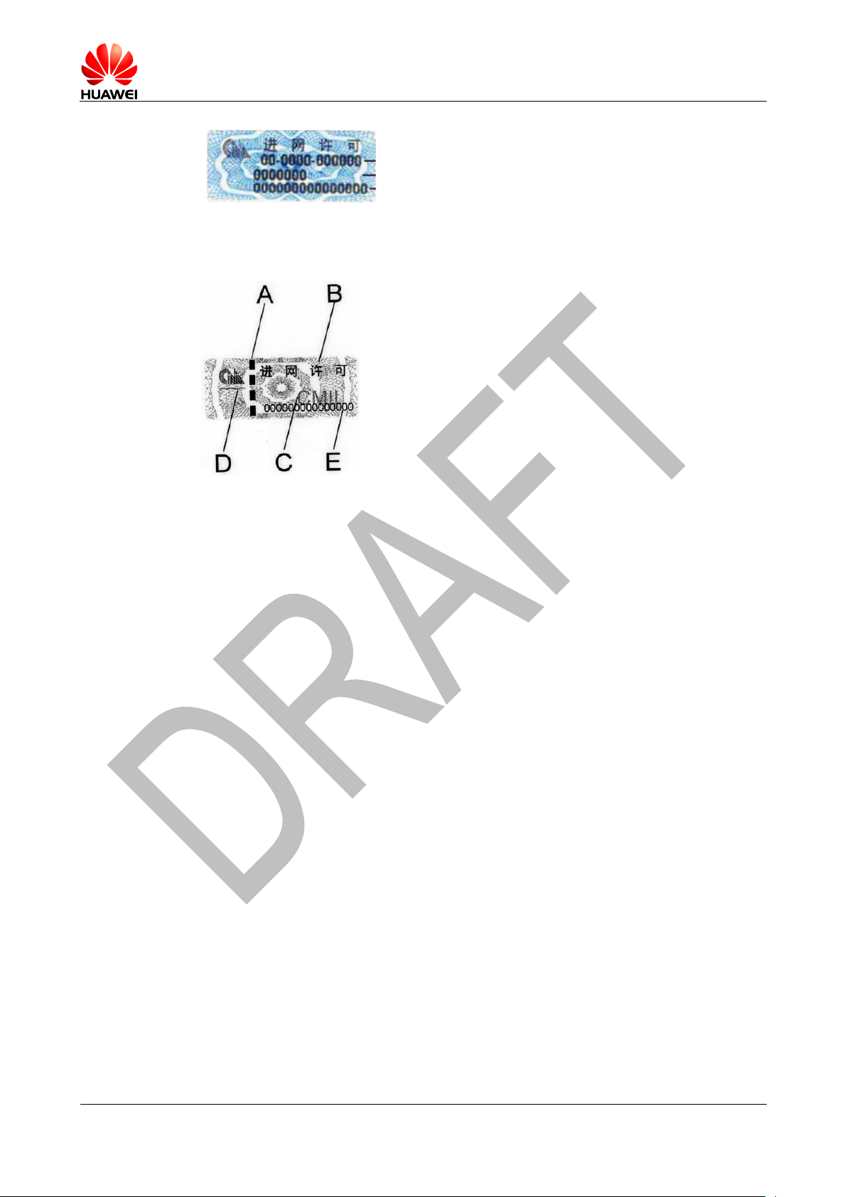
HUAWEI MC509 CDMA LGA Module
Hardware Guide
Certifications
Issue 01 (2011-04-08)
Huawei Proprietary and Confidential
Copyright © Huawei Technologies Co., Ltd.
69
License number
Equipment type
Scrambling code
The following figure shows the anti-counterfeiting measures of NAL marks.
− A means the fluorescent anti-counterfeiting string inside the mark. The anti-
counterfeiting string is visible under UV light and can be exposed with a knife.
− B means the anti-counterfeiting shading that supports anti-photography and
anti-forgery.
− C means the invisible CMII fluorescent mark that is visible under UV light.
− D means the characters that use microform printing.
− E means the unique computer scrambling code that relates to the license
number, equipment type, and sequence number. The scrambling code cannot
be copied.
Type approval
On July 24, 1995, the former State Radio Regulatory Committee (SRRC), the
State Economic and Trade Commission (SETC), the General Administration of
Customs (GAC), and the Ministry of Foreign Trade and Economic Cooperation
(MFTEC) jointly issued the Provisions on the Management of Import of Radio
Transmission Equipment. In April 1999, the Ministry of Industry and Information
Technology of the People's Republic of China (MIIT) issued the Notice of
Strengthening Management of Radio Transmission Equipment. As stipulated in
the provisions and notice, manufacturers of all radio transmission equipment
sold in China should possess the China Radio Transmission Equipment
Approval Certificate issued by the SRRC and the relevant CMIIT ID should be
affixed to the equipment nameplates.
Telecommunication equipment manufacturers should submit the China Radio
Transmission Equipment Approval Certificate when applying for a network
access license to the MIIT. In other words, completion of equipment type
approval is one of the prerequisites for network access application.
The relevant CMIIT ID should be marked on the nameplate of Huawei radio
terminals according to article 4 in the Provisions on Management of Manufacture
of Radio Transmission Equipment.
The following shows an example of the CMIIT ID:
Page 70

HUAWEI MC509 CDMA LGA Module
Hardware Guide
Certifications
Issue 01 (2011-04-08)
Huawei Proprietary and Confidential
Copyright © Huawei Technologies Co., Ltd.
70
xxxxCPxxxx
xxxx before the letters CP is four Arabic numerals, indicating the year of issue of
the certificate. xxxx following the letters CP is four Arabic numerals, indicating
the sequence number of the certificate.
CCC
The China National Certification and Accreditation Administration of People's
Republic of China (CNCA) is responsible for managing and organizing the CCC.
The CCC mark is a compulsory safety mark for the products covered in the List
of the First Group of Products Being Required Compulsory Product Certification
when the products are sold on the Chinese market. No listed product can be
imported, sold, or used in China without a CCC certificate issued by designated
certification bodies or without a CCC mark.
CCC marks are classified into standard and non-standard marks. Huawei
products use non-standard CCC marks.
RoHS, REACH, JGPSSI, and Chinese Environmental Protection
RoHS: the restriction of the use of certain hazardous substances in electrical and
electronic equipment
According to RoHS directive, all electrical and electronic products sold on the EU
market should be free of the following six hazardous substances as of July 1,
2006:
− lead
− Mercury
− Cadmium
− Hexavalent chromium
− PBB
− PBDE
The maximum permitted concentrations of the six substances are specified as
follows:
− The maximum permitted concentrations of lead, mercury, hexavalent
chromium, PBB, and PBDE are 1000 ppm (0.1%) by weight of homogeneous
material.
− The maximum permitted concentration of cadmium is limited to 100 ppm
(0.01%).
Page 71

HUAWEI MC509 CDMA LGA Module
Hardware Guide
Certifications
Issue 01 (2011-04-08)
Huawei Proprietary and Confidential
Copyright © Huawei Technologies Co., Ltd.
71
The EU does not specify any RoHS mark. Huawei, however, designs the
preceding RoHS mark to distinguish between environment-friendly and
environment-unfriendly products. For Huawei RoHS marks, any color is
acceptable.
REACH: Regulation (EC) No. 1907/2006 of the European Parliament and of the
Council of 18 December 2006 concerning the Registration, Evaluation,
Authorization and Restriction of Chemicals (REACH)
The REACH entered into force on June 1, 2007 and was implemented as of
June 1, 2008.
The REACH Regulation is a mandatory preventative regulation on all chemicals
sold on the EU market.
The REACH Regulation creates a large complex chemical management system
that transfers the chemicals safety responsibility from the government to the
industry. Manufacturers, importers, and downstream users are held responsible
for the safety of the chemicals used in their products.
The REACH Regulation specifies that a substance is regarded as hazardous
until proven safe. The earlier EU chemical regulations, however, specifies that a
substance is regarded as safe until proven hazardous.
JGPSSI: Japan Green Procurement Survey Standardization Initiative
The JGPSSI was established by some Japanese electrical and electronic
enterprises in January 2001. Since its establishment, the JGPSSI has been
researching on standardization of green procurement of electrical and electronic
products. The JGPSSI issued and promoted guidelines for management of
chemical substances in products in July 2003.
The JGPSSI divides the management of chemicals into the following three
processes:
− Acquisition of content information for purchased materials (IN information):
Obtain content information (IN information) for each substance/preparation
and each article, and confirm the reliability of the content information.
− Manufacture of products using those materials in a manufacturing process:
Increase the reliability in the daily quality management activities, such as
preventing the content of incorrect components and preventing contamination
by substances/preparations or articles that contain prohibited substances.
− Provision of content information for the products sold (OUT information):
Improve reliability by providing content information (OUT information) for each
substance/preparation or article.
China Environmental protection: Administrative Measures on the Control of
Pollution Caused by Electronic Information Products that is similar to EU's RoHS
Page 72
HUAWEI MC509 CDMA LGA Module
Hardware Guide
Certifications
Issue 01 (2011-04-08)
Huawei Proprietary and Confidential
Copyright © Huawei Technologies Co., Ltd.
72
− When designing and manufacturing electronic information products, the
manufacturers should use materials, technologies, and processes that are
easily recyclable and environment-friendly in accordance with the relevant
industrial or national standards.
− All electronic information products sold on Chinese market should be marked
with the names and contents of toxic and harmful substances and elements,
safety period, and recyclability.
− The use of six hazardous substances is prohibited or limited in the products
listed in the administrative catalogue for the control of pollution caused by
electronic information products. The catalogue is not determined at present. It
is estimated that the first catalogue is to be issued at the end of year 2009.
Printers, telephones, and mobile phones might be listed in the catalogue.
− The control of toxic and harmful substances in electronic information products
is covered in the CCC management.
− Six hazardous substances are prohibited, including lead, mercury, cadmium,
hexavalent chromium, PBB, and PBDE. Other hazardous substances defined
by China are also prohibited.
− No exemption clause is defined in the Administrative Measures on the Control
of Pollution Caused by Electronic Information Products.
The Marking for the Control of Pollution Caused by Electronic Information
Products (SJ/T11364-2006) issued on November 6, 2006 specifies that the mark
should indicate whether the electronic information products contain any toxic or
hazardous substances or elements, the safety period, and the recyclability of the
products.
− The mark shown in the left figure is used by the products that are free of any
toxic or hazardous substances or elements.
− The mark shown in the right figure is used by products that contain toxic or
hazardous substances or elements. The user manuals of the products should
indicate the names and contents of the toxic or hazardous substances or
elements. The number in the middle of the mark indicates the safety period of
the specific product. The safety period of a product will be determined in
accordance with the General Guidelines of Environment-Friendly Use Period
of Electronic Information Products to be issued.
7.3.7 Guide to Product Certification
CE Certification and FCC Certification
Huawei modules pass the RF, EMC, and safety specifications tests and obtain
relevant certificates issued by notified certification bodies.
Page 73

HUAWEI MC509 CDMA LGA Module
Hardware Guide
Certifications
Issue 01 (2011-04-08)
Huawei Proprietary and Confidential
Copyright © Huawei Technologies Co., Ltd.
73
In the case of certification of the laptops installed with Huawei modules, the relevant
test reports of Huawei modules can be directly used in accordance with the following
rules:
IC Certification
Huawei applies for IC certificate to the relevant certification bodies by using an IC test
report converted from the FCC test report.
The conductivity test data in the Huawei RF test report can be directly used by
the laptop manufacturer.
The laptop manufacturer should determine whether the radio test data in Huawei
RF test report can be used according to the antenna gain.
− The radio test data in Huawei RF test report can be directly used if the
antenna gain of the laptop is lower than that used in the certification test of
Huawei modules.
− The laptop manufacturer should test antennas of the laptops if the antenna
gain of the laptop is higher than that used in the certification test of Huawei
modules.
The laptop manufacturer should test the compliance of the laptops with EMC
and safety specifications.
The SAR of the laptops needs to be tested only if the antennas of the laptops are
within 20 cm of people.
NCC Certification
Huawei mails a sample module to the ADT of Taiwan. The ADT then performs
relevant tests and issues an NCC certificate.
7.4 GCF and PTCRB
Conformance test and declaration are required for establishing that the GSM and
WCDMA terminals to be sold in a region meet the requirements of the local carriers
and networks.
Global Certification Forum (GCF) and PTCRB certifications are recognized in most
regions all around the world. Most operators all round the world accept either
certification as one of the market entry conditions.
7.4.1 GCF Certification
The GCF is an active partnership between European mobile device manufacturers
and mobile network operators.
According to the R&TTE Directive 1999/95/EC issued in 2001, authorized test
organizations or manufacturers should perform final conformance tests of GSM
terminals in compliance with the GCF certification criteria (GCF-CC). Manufacturers
then should prepare a DOC and take all responsibilities for quality of the equipment.
The GCF officially launched the 3G WCDMA certification program in February 2005.
The GCF plays an important role in protocol and application conformance testing.
The GCF provides harmonized standards for conformance tests and defines a test
Page 74

HUAWEI MC509 CDMA LGA Module
Hardware Guide
Certifications
Issue 01 (2011-04-08)
Huawei Proprietary and Confidential
Copyright © Huawei Technologies Co., Ltd.
74
system approved by all members to ensure that the terminals meet network
deployment requirements. All GCF members approve the terminals if the terminals
are certified by the GCF. The GCF certifies both test cases and test systems. The
GCF certification originates in Europe and now is accepted by mainstream operators
in both Europe and Asia.
The GCF certification is a DOC of equipment manufacturers. Equipment
manufacturers only need to perform the test items defined by the GCF and then
submit a DOC on the GCF website. All GCF members can view the desired DOC on
the GCF website.
The test system defined by the GCF requires thorough conformance tests of
terminals. The test system consists of indoor and outdoor tests.
Outdoor tests mean field testing of terminals in actual networks. Outdoor tests
are often performed in the networks of large European operators.
Indoor tests include protocol conformance testing and application conformance
testing.
− Protocol conformance testing aims to test terminals' conformance with 3GPP
communication protocols, including GSM and WCDMA protocols.
− Application conformance testing aims to test terminals' conformance with
widely used applications such as browsers, SUPL, MMS, and VT.
The OMA and the IMTC specify operation and interaction specifications of
such upper-layer applications. Application conformance testing is based on
the test standards defined by the OMA and the IMTC.
Te rminals are not required to pass all the GCF tests. GCF tests are classified into the
following types:
Mandatory tests: Mandatory tests mean the tests that the terminals supporting
the GSM or WCDMA system must pass. Mandatory tests cover the capabilities
that a terminal must have when it supports communications in the relevant
system (GSM or WCDMA).
Optional tests: Optional tests refer to the tests that the terminals supporting a
feature specified in the 3GPP protocol or the OMA or IMTC protocols must pass.
If a manufacturer is unwilling to perform such tests for its terminals, the
manufacturer should declare that the terminals do not support the related
features and not claim that the terminals support the related features when
releasing the terminals to the market.
Unnecessary tests: The GCF does not require the terminals to pass all the tests
specified by the 3GPP, OMA, or IMTC. The tests that are not relevant need not
to be performed.
As the GCF test items need to be updated frequently to meet the requirements of
new communication technologies, the GCF updates the GCF-CC version
continuously. Usually the number of test items increases every time a new GCF-CC
version is released and terminals are required to pass an increasingly large number
of tests.
The current GCF-CC version is 3.35. The GCF updates the GCF-CC version every
two or three months. The previous version is rendered obsolete 110 days after a new
version is released. All terminal manufacturers need to pay attention to the 110-day
rule because additional test items are required after the previous version becomes
obsolete. All GCF members can view the latest GCF-CC version, the currently
available version, and the validity period published on the GCF website.
Page 75

HUAWEI MC509 CDMA LGA Module
Hardware Guide
Certifications
Issue 01 (2011-04-08)
Huawei Proprietary and Confidential
Copyright © Huawei Technologies Co., Ltd.
75
7.4.2 PTCRB Certification
The PTCRB requirements are certification standards in North America.
The PTCRB was created in March 1997. GSM 850 MHz requirements were added to
the PTCRB requirements in May 2001, which is an important development milestone
in the history of standardization organizations in U.S.A. Similar to the GCF, the
PTCRB comprises of operators and mainstream mobile phone manufacturers, and
approved laboratories. The PTCRB was created by North American operators
(Cingular, T-Mobile, and Rogers) and is applied to North America, Central America,
and South America. The PTCRB certification is similar to the GCF certification,
except that the PTCRB certification acts as the license for the UMTS terminals to be
connected to American operators' networks. Only the PTCRB certified terminals are
accepted by mainstream operators.
The PTCRB certification also differs from the GCF certification in the frequency
bands because the frequency bands used in America differ from those in Europe.
The PTCRB focuses on the GSM 850 MHz, GSM 1900 MHz, WCDMA FDD II, and
WCDMA FDD V, while the GCF focuses on the GSM 900 MHz, GSM 1800 MHz, and
WCDMA FDD I.
Different from the GCF certification, the PTCRB certification does not allow DOC.
The entire certification process should be performed under the PTCRB's supervision
and all the certification tests should be performed in the labs authorized by the
PTCRB. A manufacturer who applies for the PTCRB certification needs to submit a
test application to the PTCRB, and then the PTCRB will transfer the application to the
test organization designated by the manufacturer. The test organization should
perform the test and then submit the test report to the PTCRB for review. The PTCRB
certification is completed if the PTCRB approves the test report. The PTCRB should
also publish the certification on its website for viewing and querying by the PTCRB
members.
The PTCRB certification is similar to the GCF certification in terms of test system.
The only difference is that no field testing is performed in the case of the PTCRB
certification. OTA tests are adopted to measure the antenna performance. The
PTCRB test items and version are also updated continuously. Different from the
GCF-CC version, only one PTCRB version is valid at any time. Each PTCRB version
is valid for three months. Manufacturers are not allowed to apply for the previous
version of PTCRB certification if a new version is released. For a terminal for which
the manufacturer has applied for the previous version of PTCRB certification before
the new version is released, the manufacturer needs not to apply for the new version
if the PTCRB certification is completed within nine months.
7.4.3 Overall-System Certification
Both the test system and test items of the GCF certification are similar to those of the
PTCRB certification. Both certifications test the declared capabilities of terminals
based on the 3GPP test standards. The integrated equipment needs to pass relevant
certification tests, even though the modules pass the conformance certification. The
following describes the overall-system certification procedures in detail. The overallsystem can be a notebook, a MID, a smartphone, etc.
Page 76

HUAWEI MC509 CDMA LGA Module
Hardware Guide
Certifications
Issue 01 (2011-04-08)
Huawei Proprietary and Confidential
Copyright © Huawei Technologies Co., Ltd.
76
Overall-System GCF Certification
Huawei modules pass the GCF certification before being released to the market.
Huawei performs 2000 to 3000 test items for each type of modules. The major tests
are as follows:
Protocol conformance test
RF conformance test
UIM conformance test
The details about the certification tests are defined in the 3GPP test standards.
According to the GCF-CC, the test reports of modules can be used for the overallsystem certification. The changed parts, however, need to be re-tested. Regarding
the product structure, the antennas and UIM card interface circuits are modified in the
integrated equipment. For this reason, the antennas and the UIM card interface
circuits need to be re-tested in the overall-system certification.
Field test
The antenna performance-relevant field test is required due to changes in the
antennas and to test the equipment's functions and its interoperability with
networks on five networks run by different European operators. To be specific,
the field test tests the basic functions of the UE on actual networks and
determines whether the UE passes the testing according to the UE performance.
UIM test
UIM card interface circuits are re-designed in the integrated equipment, which
may result in changes in the electrical features of the UIM card interface. For this
reason, the UIM card interface circuits need to be re-tested. The UIM test aims
to verify the overall performance of UIM interface with appropriate test
instruments in accordance with the relevant 3GPP protocol requirements.
Huawei provides a test report of the product to be certified for the customers who
require the GCF certification. The test report is issued by an organization designated
for GCF certification. The test report covers the Protocol Implementation
Conformance Statement (PICS) and the test information on the product. The PICS is
a conformance statement of the product and a basis for GCF certification. The test
information includes the performed test items and results of the product. The test
organization can issue a certification report of the integrated equipment after
performing the required field test and UIM test based on the test report provided by
Huawei.
Terminal manufacturers who apply for the GCF certification of the terminals to be
integrated with Huawei modules must accomplish the following tasks:
1. Register as a member of the GCF.
The GCF certification is a DOC. Only GCF members can submit their DOC on
the GCF website. Contact the GCF if you need to join the GCF. Proceed with the
following steps if you are a GCF member.
2. Choose a test organization.
The GCF does not designate its test organizations. All test organizations that
meet the GCF test conditions can perform GCF tests. In this case, it is
necessary for manufacturers to choose a well-recognized test organization that
provides high quality and high efficiency services. The global test organizations
7layers, SGS, and CETCOM are recommended. The recommended test
organizations have built various labs all around the world and work closely with
Page 77

HUAWEI MC509 CDMA LGA Module
Hardware Guide
Certifications
Issue 01 (2011-04-08)
Huawei Proprietary and Confidential
Copyright © Huawei Technologies Co., Ltd.
77
the GCF and the PTCRB. Therefore, the test organizations are able to provide
high quality and high efficiency test services and are widely recognized by
operators.
3. Discuss test details with the test organization.
Provide the test organization with the test report of Huawei modules and the
modifications of the integrated equipment. The test organization then can
determine the detailed test items and determine the test schedule accordingly.
With the detailed test items and schedule, terminal manufacturers can determine
accurate plans of product development and marketing.
4. Perform overall-system certification.
The integrated equipment can pass the over-all certification test easily if
Huawei's design suggestions are complied with.
5. Obtain the test report and the DOC.
The test report describes the details about the overall-system test that operators
are concerned about. The GCF certification is completed upon uploading of the
DOC to the GCF website.
Overall-System PTCRB Certification
Huawei modules pass the PTCRB certification before being released to the market.
Huawei performs 2000 to 3000 test items for each type of modules. The major tests
are as follows:
Protocol conformance test
RF conformance test
UIM conformance test
The details about the certification tests are defined in the 3GPP test standards.
According to the PTCRB certification criteria, the test reports of modules can be used
for the overall-system certification. The changed parts, however, need to be re-tested.
Regarding the product structure, the antennas and UIM card interface circuits are
modified in the integrated equipment. For this reason, the antennas and the UIM card
interface circuits need to be re-tested in the overall-system certification.
OTA test
Different from the GCF certification, the PTCRB certification does not require
field testing. The antenna performance is verified through OTA tests. OTA tests
are defined by the CTIA for verifying antenna performance.
UIM test
UIM card interface circuits are re-designed in the integrated equipment, which
may result in changes in the electrical features of the UIM card interface. For this
reason, the UIM card interface circuits need to be re-tested. The UIM test aims
to verify the overall performance of UIM interface with appropriate test
instruments in accordance with the relevant 3GPP protocol requirements.
Similar to the GCF certification, the PTCRB certification requires a small number of
test items for integrated equipment. In addition, the required test items are easy to
perform with appropriate design suggestions. Huawei also provides customers with a
PTCRB test report of the module. The test is a basis for the PTCRB certification of
the equipment integrated with the module.
Page 78

HUAWEI MC509 CDMA LGA Module
Hardware Guide
Certifications
Issue 01 (2011-04-08)
Huawei Proprietary and Confidential
Copyright © Huawei Technologies Co., Ltd.
78
Terminal manufacturers who apply for the PTCRB certification of the terminals to be
integrated with Huawei modules must accomplish the following tasks:
1. Register as a guest of the PTCRB.
Different from the GCF, the PTCRB comprises of only operators. Terminal
manufacturers can join the PTCRB only as guests. The terminal manufacturers
who apply for the PTCRB certification have to register as PTCRB guests as they
must submit the application on the PTCRB website.
2. Choose a test organization.
The PTCRB requires only qualified test organization to perform PTCRB tests. In
this case, it is necessary for manufacturers to choose a well-recognized test
organization that provides high quality and high efficiency services. The global
test organizations 7layers, SGS, and CETCOM are recommended. The
recommended test organizations have built various labs all around the world and
work closely with the GCF and the PTCRB. Therefore, the test organizations are
able to provide high quality and high efficiency test services and are widely
recognized by operators.
3. Discuss test details with the test organization.
Provide the test organization with the test report of Huawei modules and the
modifications of the integrated equipment. The test organization then can
determine the detailed test items and determine the test schedule accordingly.
With the detailed test items and schedule, terminal manufacturers can determine
accurate plans of product development and marketing.
4. Submit an overall-system certification application on the PTCRB website and designate a test organization.
Submit a test application on the PTCRB website, indicating the basic information
of the terminal to be certified. The PTCRB then transfers the application to the
designated test organization. Remember to pay the CTIA after you submit a test
application. Unpaid applications are rejected even though all the required tests
are performed.
5. Perform overall-system certification.
The integrated equipment can pass the over-all certification test easily if
Huawei's design suggestions are complied with.
6. Obtain the test report and submit relevant materials.
The PTCRB test report is provided by the test organization. The terminal
manufacturer, however, is required to provide the user manual and other
necessary documents of the terminal to be certified on the PTCRB website
before the PTCRB test application can be approved. In addition, the PTCRB
submits all the materials to the CTIA for review on completion of all the PTCRB
tests. The terminal is PTCRB certified on completion of the CTIA review.
GCF and PTCRB Certification
To launch a terminal in the global market, both the GCF certification and the PTCRB
certification are required. In this case, the manufacturer does not need to conduct two
end-to-end tests. As the UIM test is the same for both the GCF certification and the
PTCRB certification, the test organization needs to perform the UIM test only once.
This practice is recognized by both the GCF and the PTCRB. The cost, including time
and expense, of overall-system certification is thus reduced.
Page 79

HUAWEI MC509 CDMA LGA Module
Hardware Guide
Safety Information
Issue 01 (2011-04-08)
Huawei Proprietary and Confidential
Copyright © Huawei Technologies Co., Ltd.
79
Read the safety information carefully to ensure the correct and safe use of your
wireless device. Applicable safety information must be observed.
8.1 Interference
8 Safety Information
Power off your wireless device if using the device is prohibited. Do not use the
wireless device when it causes danger or interference with electric devices.
8.2 Medical Device
Power off your wireless device and follow the rules and regulations set forth by
the hospitals and health care facilities.
Some wireless devices may affect the performance of the hearing aids. For any
such problems, consult your service provider.
Pacemaker manufacturers recommend that a minimum distance of 15 cm be
maintained between the wireless device and a pacemaker to prevent potential
interference with the pacemaker. If you are using an electronic medical device,
consult the doctor or device manufacturer to confirm whether the radio wave
affects the operation of this device.
8.3 Area with Inflammables and Explosives
To prevent explosions and fires in areas that are stored with inflammable and
explosive devices, power off your wireless device and observe the rules. Areas
stored with inflammables and explosives include but are not limited to the following:
Gas station
Fuel depot (such as the bunk below the deck of a ship)
Container/Vehicle for storing or transporting fuels or chemical products
Area where the air contains chemical substances and particles (such as granule,
dust, or metal powder)
Page 80

HUAWEI MC509 CDMA LGA Module
Hardware Guide
Safety Information
Issue 01 (2011-04-08)
Huawei Proprietary and Confidential
Copyright © Huawei Technologies Co., Ltd.
80
Area indicated with the "Explosives" sign
Area indicated with the "Power off bi-direction wireless equipment" sign
Area where you are generally suggested to stop the engine of a vehicle
8.4 Traffic Security
Observe local laws and regulations while using the wireless device. To prevent
accidents, do not use your wireless device while driving.
RF signals may affect electronic systems of motor vehicles. For more information,
consult the vehicle manufacturer.
In a motor vehicle, do not place the wireless device over the air bag or in the air
bag deployment area. Otherwise, the wireless device may hurt you owing to the
strong force when the air bag inflates.
8.5 Airline Security
Observe the rules and regulations of airline companies. When boarding or
approaching a plane, power off your wireless device. Otherwise, the radio signal of
the wireless device may interfere with the plane control signals.
8.6 Safety of Children
Do not allow children to use the wireless device without guidance. Small and sharp
components of the wireless device may cause danger to children or cause
suffocation if children swallow the components.
8.7 Environment Protection
Observe the local regulations regarding the disposal of your packaging materials,
used wireless device and accessories, and promote their recycling.
8.8 WEEE Approval
The wireless device is in compliance with the essential requirements and other
relevant provisions of the Waste Electrical and Electronic Equipment Directive
2002/96/EC (WEEE Directive).
8.9 RoHS Approval
The wireless device is in compliance with the restriction of the use of certain
hazardous substances in electrical and electronic equipment Directive 2002/95/EC
(RoHS Directive).
Page 81

HUAWEI MC509 CDMA LGA Module
Hardware Guide
Safety Information
Issue 01 (2011-04-08)
Huawei Proprietary and Confidential
Copyright © Huawei Technologies Co., Ltd.
81
8.10 Laws and Regulations Observance
Observe laws and regulations when using your wireless device. Respect the privacy
and legal rights of the others.
8.11 Care and Maintenance
It is normal that your wireless device gets hot when you use or charge it. Before you
clean or maintain the wireless device, stop all applications and power off the wireless
device.
Use your wireless device and accessories with care and in clean environment.
Keep the wireless device from a fire or a lit cigarette.
Protect your wireless device and accessories from water and vapour and keep
them dry.
Do not drop, throw or bend your wireless device.
Clean your wireless device with a piece of damp and soft antistatic cloth. Do not
use any chemical agents (such as alcohol and benzene), chemical detergent, or
powder to clean it.
Do not leave your wireless device and accessories in a place with a considerably
low or high temperature.
Use only accessories of the wireless device approved by the manufacture.
Contact the authorized service center for any abnormity of the wireless device or
accessories.
Do not dismantle the wireless device or accessories. Otherwise, the wireless
device and accessories are not covered by the warranty.
8.12 Emergency Call
This wireless device functions through receiving and transmitting radio signals.
Therefore, the connection cannot be guaranteed in all conditions. In an emergency,
you should not rely solely on the wireless device for essential communications.
8.13 Specific Absorption Rate (SAR)
Your wireless device is a radio transmitter and receiver. It is designed not to exceed
the limits for exposure to radio waves recommended by international guidelines.
These guidelines were developed by the independent scientific organization ICNIRP
and include safety margins designed to assure the protection of all persons,
regardless of age and health.
The guidelines use a unit of measurement known as the Specific Absorption Rate, or
SAR. The SAR limit for wireless devices is 2.0 W/kg and the highest SAR value for
this device when tested complied with this limit.
Page 82

HUAWEI MC509 CDMA LGA Module
Hardware Guide
Safety Information
Issue 01 (2011-04-08)
Huawei Proprietary and Confidential
Copyright © Huawei Technologies Co., Ltd.
82
8.14 Regulatory Information
The following approvals and notices apply in specific regions as noted.
8.14.1 CE Approval (European Union)
The wireless device is approved to be used in the member states of the EU. The
wireless device is in compliance with the essential requirements and other relevant
provisions of the Radio and Telecommunications Terminal Equipment Directive
1999/5/EC (R&TTE Directive).
Federal Communications Commission Notice (United States): Before a wireless
device model is available for sale to the public, it must be tested and certified to the
FCC that it does not exceed the limit established by the government-adopted
requirement for safe exposure.
The SAR limit adopted by the USA and Canada is 1.6 watts/kilogram (W/kg)
averaged over one gram of tissue. The highest SAR value reported to the FCC for
this device type was compliant with this limit.
8.14.2 FCC Statement
This device complies with Part 15 of the FCC Rules. Operation is subject to the
following two conditions: (1) this device may not cause harmful interference, and (2)
this device must accept any interference received, including interference that may
cause undesired operation.
The antenna(s) used for this transmitter must be installed to provide a separation
distance of at least 20 cm from all persons.
Warning: Changes or modifications made to this equipment not expressly approved
by HUAWEI may void the FCC authorization to operate this equipment
Page 83
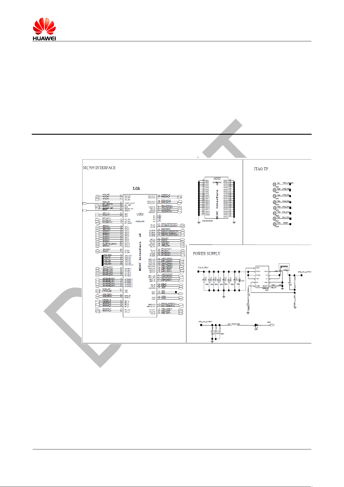
HUAWEI MC509 CDMA LGA Module
Hardware Guide
Appendix A Circuit of Typical Interfaces
Issue 01 (2011-04-08)
Huawei Proprietary and Confidential
Copyright © Huawei Technologies Co., Ltd.
83
9 Appendix A Circuit of Typical Interfaces
Page 84
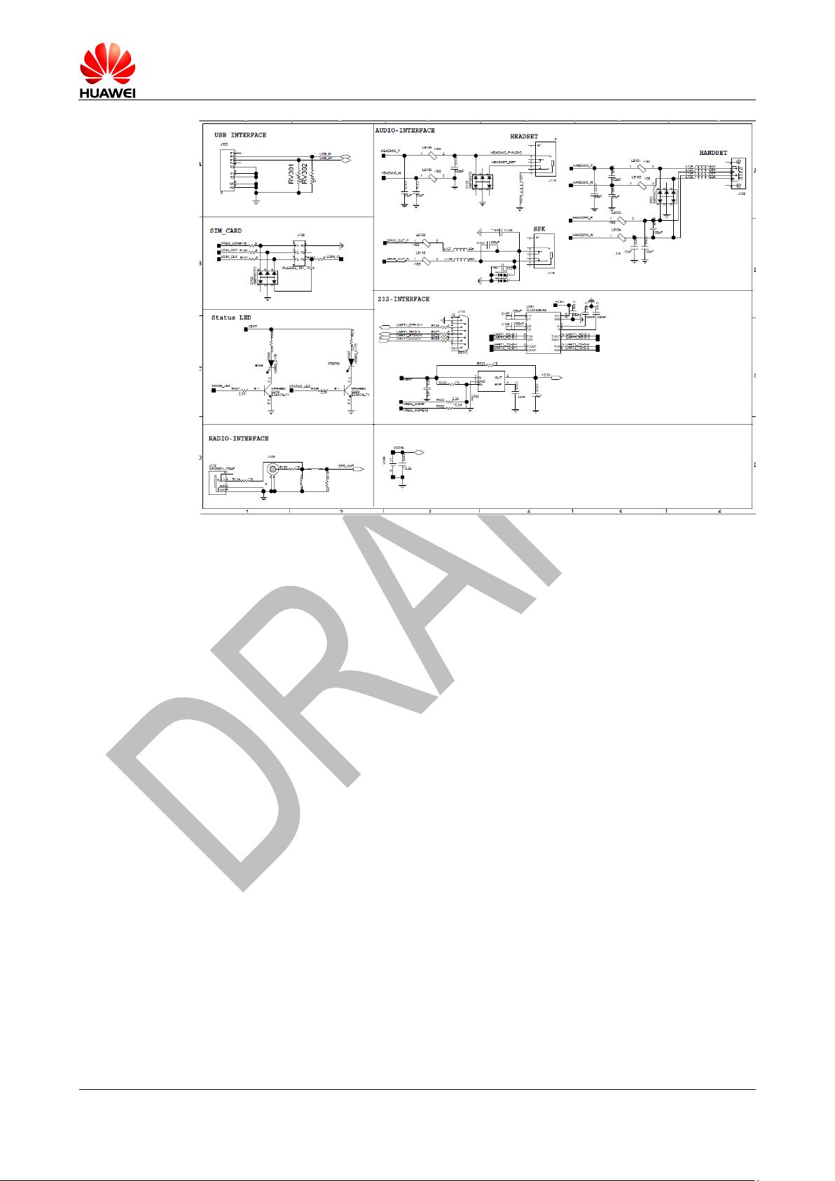
HUAWEI MC509 CDMA LGA Module
Hardware Guide
Appendix A Circuit of Typical Interfaces
Issue 01 (2011-04-08)
Huawei Proprietary and Confidential
Copyright © Huawei Technologies Co., Ltd.
84
Page 85
HUAWEI MC509 CDMA LGA Module
Hardware Guide
Appendix B Acronyms and Abbreviations
Issue 01 (2011-04-08)
Huawei Proprietary and Confidential
Copyright © Huawei Technologies Co., Ltd.
85
10 Appendix B Acronyms and
Acronym or Abbreviation
Expansion
BB
Baseband
CE
European Conformity
CS
Coding Scheme
CSD
Circuit Switched Data
DC
direct current
DCE
data circuit-terminating equipment
DMA
direct memory access
DTE
data terminal equipment
EIA
Electronic Industries Association
EMC
electromagnetic compatibility
ESD
electrostatic discharge
FCC
Federal Commnications Commission
ISO
International Standards Organization
LCP
liquid crystal polyester
LDO
low-dropout
LED
light-emitting diode
MCP
multi-chip package
NTC
negative temperature coefficient
PBCCH
Packet Broadcast Control Channel
PCB
printed circuit board
Abbreviations
Page 86
HUAWEI MC509 CDMA LGA Module
Hardware Guide
Appendix B Acronyms and Abbreviations
Issue 01 (2011-04-08)
Huawei Proprietary and Confidential
Copyright © Huawei Technologies Co., Ltd.
86
Acronym or Abbreviation
Expansion
PDU
protocol data unit
RF
radio frequency
RoHS
Restriction of the use of certain Hazardous
Substances
RTC
real-time clock
UIM
User interface module
TTL
transistor-transistor logic
TVS
transient voltage suppressor
VSWR
voltage standing wave ratio
ACLR
Adjacent channel leakage power radio
AMPS
Advanced mobile phone system
CDMA
Code-division multiple access
DCCH
Dedicated control channel
EACH
Enhanced access channel
EVRC
Enhanced variable rate coder
LNA
Low noise amplifier
LPF
Lowpass filter
NF
Noise figure
PCM
Pulse coded modulation
PCS
Personal communication system
PLL
Phase lock loop
RF
Radio frequncy
Rx
Receive
SCH
Supplemental channel
SYNCH
Sync channel
EVDO
Evolution data only
 Loading...