

Page 1

Technical Reference Manual
Hardware and BIOS
HP KAYAK XA PC WORKSTATION
Page 2

Notice
The information contained in this document is subject to change without notice.
Hewlett-Packard makes no warranty of any kind with regard to this
material, including, but not limited to, the implied warranties of
merchantability and fitness for a particular purpose.
Hewlett-Packard shall not be liable for errors contained herein or for incidental
or consequential damages in connection with the furnishing, performance, or use
of this material.
Hewlett-Packard assumes no responsibility for the use or reliability of its
software on equipment that is not furnished by Hewlett-Packard.
This document contains proprietary information that is protected by copyright.
All rights are reserved. No part of this document may be photocopied,
reproduced, or translated to another language without the prior written consent
of Hewlett-Packard Company.
TM
Adobe
in certain jurisdictions.
Microsoft®, Windows® and MS-DOS® are U.S. registered trademarks of
Microsoft Corporation.
MMX
Netscape
is a trademark of Adobe Systems Incorporated which may be registered
TM
is a U.S. trademark of Intel Corporation.
TM
is a U.S. trademark of Netscape Communications Corporation.
Pentium® is a U.S. registered trademark of Intel Corporation.
SoundBlaster
TM
is a trademark of Creative Technology Limited.
Windows NT® is a registered trademark of Microsoft Corporation.
Hewlett-Packard France
38053 Grenoble Cedex 9
France
Page 3

Preface
This manual is a technical reference and BIOS document for engineers and
technicians providing system level support. It is assumed that the reader
possesses a detailed understanding of AT-compatible microprocessor
functions and digital addressing techniques.
Technical information that is readily available from other sources, such as
manufacturer’s proprietary publications, has not been reproduced.
This manual contains summary information only. For additional reference
material, refer to the bibliography, on the next page.
Conventions
The following conventions are used throughout this manual to identify
specific numeric elements:
❒ Hexadecimal numbers are identified by a lower case h.
For example, 0FFFFFFFh or 32F5h
❒ Binary numbers and bit patterns are identified by a lower case b.
For example, 1101b or 10011011b
3
Page 4

Bibliography
❒ HP Kayak XA PC Workstation DT User’s Guide manual (D4790-90001).
❒ HP Kayak XA PC Workstation MT User’s Guide manual (D4800-90001).
❒ HP Kayak XA PC Workstation (Desktop and Minitower) Familiarization
Guide (online - D4790-90901).
❒ HP Network Administrator’s Guide (online).
❒ HP Kayak XA PC Workstation Service Handbook -
1st edition (5966-8261).
❒ HP Support Assistant CD-ROM (by subscription).
Data sheets can be obtained at:
❒ Analog AD1816 (sound card controller)
http:\\www.analog.com\products\sheets\ad1816a.html.
❒ Cirrus 5465 (graphic controller)
http:\\www.cirus.com\products\categories\graphicsvid.html.
❒ Intel Chipsets. 440LX AGPSet (82443LX) and,
PIIX4 PCI/ISA Bridge Chip
http:\\www.intel.com\pcisets\datashts\index.html.
(82371SB)
❒ Memory
http:\\www.chips.ibm.com\products\memory\sdamart\sdramart.html.
❒ Pentium II Processor
http:\\www.intel.com\design\pcisets\datashts\index.html.
❒ SCSI Chips
http:\\www.symbios.com\products\scsichps.html.
❒ Super I/O
http:\\www.national.com\catalog\personal_superi_desktop.html.
For further information about the availability and where to find the different
documentation, refer to page 21
.
4
Page 5

How to use this online guide
A
A
A
A
A
A
A
A
A
A
A
A
A
A
A
AAAA
AAAA
AAAA
AAAA
A
A
A
A
A
A
A
A
A
A
A
A
A
A
A
A
A
A
A
A
A
A
A
A
A
A
A
A
A
A
A
AAAA
AAAA
AAAA
AAAA
A
A
A
A
A
A
A
A
A
A
A
A
A
A
A
A
A
A
A
A
A
A
A
A
A
A
A
A
A
A
A
AAAA
AAAA
AAAA
AAAA
A
A
A
A
A
A
A
A
A
A
A
A
A
A
A
A
A
A
A
A
A
A
A
A
A
A
A
A
A
A
A
AAAA
AAAA
AAAA
AAAA
A
A
A
A
A
A
A
A
A
A
A
A
A
A
A
A
AAA
AAAA
AAAA
AAAA
AAA
AAAA
AAAA
AAAA
AAA
AAAA
AAAA
AAAA
AAA
AAAA
AAAA
AAAA
AAA
AAAA
AAAA
AAAA
AAA
AAAA
AAAA
AAAA
AAA
AAAA
AAAA
AAAA
AAA
AAAA
AAAA
AAAA
AAA
AAAA
AAAA
AAAA
AAA
AAAA
AAAA
AAAA
AAA
AAAA
AAAA
AAAA
AAA
AAAA
AAAA
AAAA
AAA
AAAA
AAAA
AAAA
AAA
AAAA
AAAA
AAAA
AAA
AAAA
AAAA
AAAA
AAA
AAAA
AAAA
AAAA
AAA
AAAA
AAAA
AAAA
AAA
AAAA
AAAA
AAAA
AAA
AAAA
AAAA
AAAA
AAA
AAAA
AAAA
AAAA
AAA
AAAA
AAAA
AAAA
AAA
AAAA
AAAA
AAAA
AAA
AAAA
AAAA
AAAA
AAA
AAAA
AAAA
AAAA
AAA
AAAA
AAAA
AAAA
AAA
AAAA
AAAA
AAAA
AAA
AAAA
AAAA
AAAA
AAA
AAAA
AAAA
AAAA
AAA
AAAA
AAAA
AAAA
AAA
AAAA
AAAA
AAAA
AAA
AAAA
AAAA
AAAA
AAA
AAAA
AAAA
AAAA
AAA
AAAA
AAAA
AAAA
AAA
AAAA
AAAA
AAAA
AAA
AAAA
AAAA
AAAA
AAA
AAAA
AAAA
AAAA
AAA
AAAA
AAAA
AAAA
AAA
AAAA
AAAA
AAAA
AAA
AAAA
AAAA
AAAA
AAA
AAAA
AAAA
AAAA
AAA
AAAA
AAAA
AAAA
AAA
AAAA
AAAA
AAAA
AAA
AAAA
AAAA
AAAA
AAA
AAAA
AAAA
AAAA
AAA
AAAA
AAAA
AAAA
AAA
AAAA
AAAA
AAAA
AAA
AAAA
AAAA
AAAA
AAA
AAAA
AAAA
AAAA
AAA
AAAA
AAAA
AAAA
AAA
AAAA
AAAA
AAAA
AAA
AAAA
AAAA
AAAA
AAA
AAAA
AAAA
AAAA
AAA
AAAA
AAAA
AAAA
AAA
AAAA
AAAA
AAAA
AAA
AAAA
AAAA
AAAA
AAA
AAAA
AAAA
AAAA
AAA
AAAA
AAAA
AAAA
AAA
AAAA
AAAA
AAAA
AAA
AAAA
AAAA
AAAA
AAA
AAAA
AAAA
AAAA
Click the Go Back button in the toolbar to go back to your previous place in
the guide.
Click the Next Page button in the toolbar to go to the next page in the
guide.
Click the Previous Page button in the toolbar to go to the previous page
in the guide.
Click the First Page button in the toolbar to go to the opening screen of
the guide.
System Overv iew
External Feature s
Specifications
Hardware Control Panel
Documentation
Topic
Click a bookmark name (to the left of the screen) to go to the topic
corresponding to that bookmark. Clicking a right-pointing triangle,
for example, will reveal the subordinate bookmarks. Clicking a
downward pointing triangle will hide the subordinate bookmarks.
Click underlined red text to go to the topic indicated. Underlined red
text is text that is “linked” to another topic in the guide.
5
Page 6

6
Page 7

Contents
Preface . . . . . . . . . . . . . . . . . . . . . . . . . . . . . . . . . . . . . . . . . . . . . . . . . . . 3
Conventions. . . . . . . . . . . . . . . . . . . . . . . . . . . . . . . . . . . . . . . . . . . . . . . 3
Bibliography. . . . . . . . . . . . . . . . . . . . . . . . . . . . . . . . . . . . . . . . . . . . . . . 4
How to use this online guide . . . . . . . . . . . . . . . . . . . . . . . . . . . . . . . . . 5
1 System Overview
Package for the Desktop Models . . . . . . . . . . . . . . . . . . . . . . . . . . . . 12
Package for the Minitower Models. . . . . . . . . . . . . . . . . . . . . . . . . . . 13
HP Kayak XA PC Workstation Overview . . . . . . . . . . . . . . . . . . . . . . 14
Hardware Control Panel. . . . . . . . . . . . . . . . . . . . . . . . . . . . . . . . . . . . 15
Specifications and Characteristic Data . . . . . . . . . . . . . . . . . . . . . . . 16
Physical Characteristics . . . . . . . . . . . . . . . . . . . . . . . . . . . . . . . . . . . . . . 16
Electrical Specifications . . . . . . . . . . . . . . . . . . . . . . . . . . . . . . . . . . . . . . 16
Environmental Specifications (Desktop and Minitower) . . . . . . . . . . . . 20
Documentation . . . . . . . . . . . . . . . . . . . . . . . . . . . . . . . . . . . . . . . . . . . 21
Where to Find the Information. . . . . . . . . . . . . . . . . . . . . . . . . . . . . . . . . 22
2 System Board
System Board and Backplane Boards . . . . . . . . . . . . . . . . . . . . . . . . 26
Architectural View . . . . . . . . . . . . . . . . . . . . . . . . . . . . . . . . . . . . . . . . 29
Chip-Set . . . . . . . . . . . . . . . . . . . . . . . . . . . . . . . . . . . . . . . . . . . . . . . . . 30
The PAC Chip (440LX). . . . . . . . . . . . . . . . . . . . . . . . . . . . . . . . . . . . . . . 30
The PIIX4, PCI/ISA Bridge Chip (82371AB) . . . . . . . . . . . . . . . . . . . . . . 32
7
Page 8

Contents
Cache Memory . . . . . . . . . . . . . . . . . . . . . . . . . . . . . . . . . . . . . . . . . . . . . 34
Devices on the Processor-Local Bus. . . . . . . . . . . . . . . . . . . . . . . . . . 35
Intel Pentium II Microprocessor . . . . . . . . . . . . . . . . . . . . . . . . . . . . . . . 35
Main Memory Bus . . . . . . . . . . . . . . . . . . . . . . . . . . . . . . . . . . . . . . . . . 38
Devices on the PCI Bus. . . . . . . . . . . . . . . . . . . . . . . . . . . . . . . . . . . . . 39
Integrated Drive Electronics (IDE). . . . . . . . . . . . . . . . . . . . . . . . . . . . . 39
Universal Serial Bus (USB) Controller . . . . . . . . . . . . . . . . . . . . . . . . . . 40
Other PCI Accessory Devices . . . . . . . . . . . . . . . . . . . . . . . . . . . . . . . . . 40
Accelerated Graphics Port (AGP) Controller . . . . . . . . . . . . . . . . . . 41
Devices on the SM Bus . . . . . . . . . . . . . . . . . . . . . . . . . . . . . . . . . . . . . 43
Serial EEPROM. . . . . . . . . . . . . . . . . . . . . . . . . . . . . . . . . . . . . . . . . . . . . 43
LM75 Chip. . . . . . . . . . . . . . . . . . . . . . . . . . . . . . . . . . . . . . . . . . . . . . . . . 44
Main PLL. . . . . . . . . . . . . . . . . . . . . . . . . . . . . . . . . . . . . . . . . . . . . . . . . . 44
Devices on the ISA Bus. . . . . . . . . . . . . . . . . . . . . . . . . . . . . . . . . . . . . 45
The Super I/O Controller (NS 82317) . . . . . . . . . . . . . . . . . . . . . . . . . . . 45
Audio Controller. . . . . . . . . . . . . . . . . . . . . . . . . . . . . . . . . . . . . . . . . . . . 46
Flash EEPROM . . . . . . . . . . . . . . . . . . . . . . . . . . . . . . . . . . . . . . . . . . . . . 47
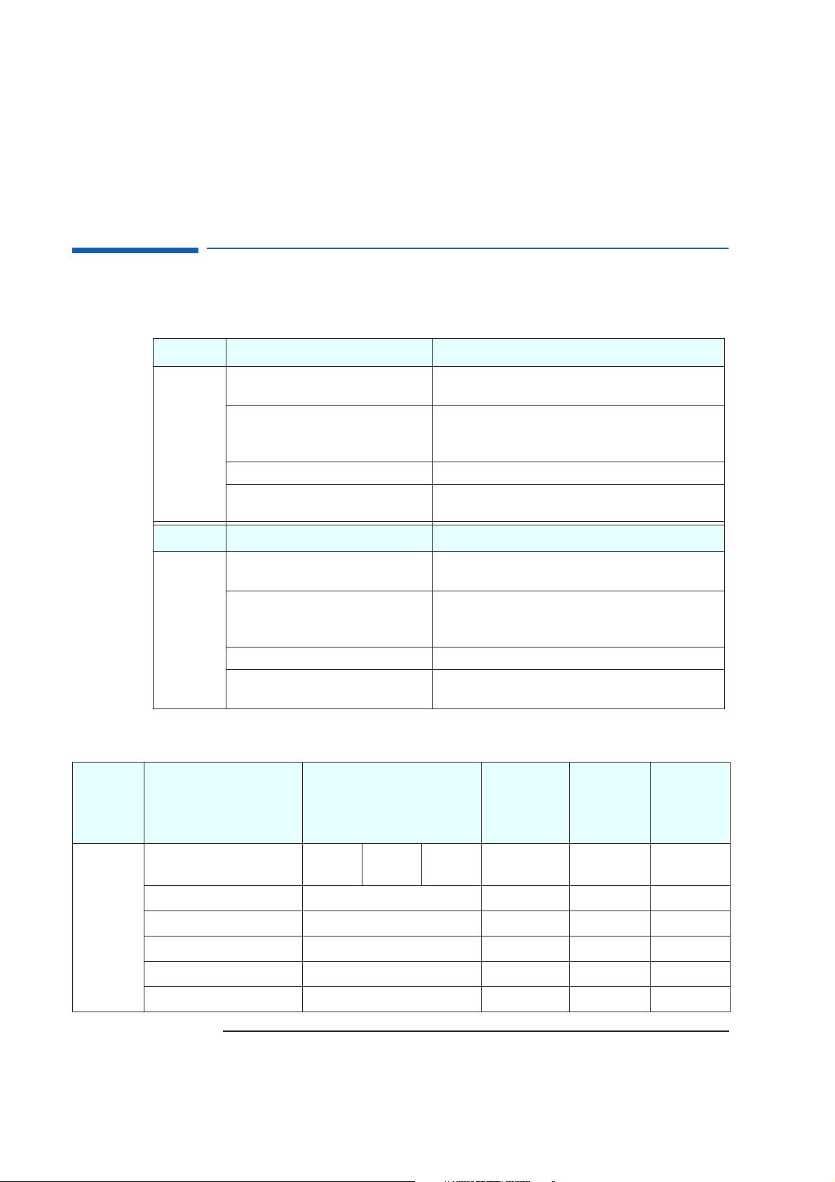
System Board Switches . . . . . . . . . . . . . . . . . . . . . . . . . . . . . . . . . . . . . . 48
Little Ben . . . . . . . . . . . . . . . . . . . . . . . . . . . . . . . . . . . . . . . . . . . . . . . . . 50
Other ISA Accessory Devices . . . . . . . . . . . . . . . . . . . . . . . . . . . . . . . . . 51
3 Interface Devices and Mass-Storage Drives
Cirrus 5465 Graphics Controller Chip. . . . . . . . . . . . . . . . . . . . . . . . . 54
Connectors . . . . . . . . . . . . . . . . . . . . . . . . . . . . . . . . . . . . . . . . . . . . . . . . 56
Video Memory. . . . . . . . . . . . . . . . . . . . . . . . . . . . . . . . . . . . . . . . . . . . . . 56
Available Video Resolutions . . . . . . . . . . . . . . . . . . . . . . . . . . . . . . . . . . . 57
SCSI / LAN Combo Board. . . . . . . . . . . . . . . . . . . . . . . . . . . . . . . . . . . 58
8
Page 9

Contents
PCI Interface . . . . . . . . . . . . . . . . . . . . . . . . . . . . . . . . . . . . . . . . . . . . . . . 58
SCSI Interface . . . . . . . . . . . . . . . . . . . . . . . . . . . . . . . . . . . . . . . . . . . . . . 59
SCSI / PCI LAN Combo Board Features . . . . . . . . . . . . . . . . . . . . . . . . . 60
10BT/100TX LAN Controller . . . . . . . . . . . . . . . . . . . . . . . . . . . . . . . . 61
10BT/100TX LAN Features . . . . . . . . . . . . . . . . . . . . . . . . . . . . . . . . . . . 62
Remote Power On . . . . . . . . . . . . . . . . . . . . . . . . . . . . . . . . . . . . . . . . . . . 62
Mass-Storage Drives . . . . . . . . . . . . . . . . . . . . . . . . . . . . . . . . . . . . . . . 64
Hard Disk Drives . . . . . . . . . . . . . . . . . . . . . . . . . . . . . . . . . . . . . . . . . . . . 64
Flexible Disk Drives . . . . . . . . . . . . . . . . . . . . . . . . . . . . . . . . . . . . . . . . . 64
CD-ROM Drives . . . . . . . . . . . . . . . . . . . . . . . . . . . . . . . . . . . . . . . . . . . . . 65
Connectors and Sockets. . . . . . . . . . . . . . . . . . . . . . . . . . . . . . . . . . . . 66
4 HP BIOS
HP/Phoenix BIOS Summary . . . . . . . . . . . . . . . . . . . . . . . . . . . . . . . . 74
Using the HP Setup Program . . . . . . . . . . . . . . . . . . . . . . . . . . . . . . . . . . 74
Main Menu . . . . . . . . . . . . . . . . . . . . . . . . . . . . . . . . . . . . . . . . . . . . . . . . . 74
Advanced Menu . . . . . . . . . . . . . . . . . . . . . . . . . . . . . . . . . . . . . . . . . . . . . 75
Security . . . . . . . . . . . . . . . . . . . . . . . . . . . . . . . . . . . . . . . . . . . . . . . . . . . 76
Boot Menu . . . . . . . . . . . . . . . . . . . . . . . . . . . . . . . . . . . . . . . . . . . . . . . . . 76
Power Menu . . . . . . . . . . . . . . . . . . . . . . . . . . . . . . . . . . . . . . . . . . . . . . . . 76
Symbios Logic SCSI Configuration Utility. . . . . . . . . . . . . . . . . . . . . 77
Default Settings You Can Change. . . . . . . . . . . . . . . . . . . . . . . . . . . . . . . 77
Starting the SCSI Configuration Utility . . . . . . . . . . . . . . . . . . . . . . . . . . 78
Power Saving and Ergonometry . . . . . . . . . . . . . . . . . . . . . . . . . . . . . 79
Power-On from Space-Bar . . . . . . . . . . . . . . . . . . . . . . . . . . . . . . . . . . . . 79
Soft Power Down. . . . . . . . . . . . . . . . . . . . . . . . . . . . . . . . . . . . . . . . . . . . 79
BIOS Addresses. . . . . . . . . . . . . . . . . . . . . . . . . . . . . . . . . . . . . . . . . . . 80
System Memory Map. . . . . . . . . . . . . . . . . . . . . . . . . . . . . . . . . . . . . . . . . 80
9
Page 10

Contents
HP I/O Port Map (I/O Addresses Used by the System) . . . . . . . . . . . . . 81
DMA Channel Controllers. . . . . . . . . . . . . . . . . . . . . . . . . . . . . . . . . . . . . 82
Interrupt Controllers . . . . . . . . . . . . . . . . . . . . . . . . . . . . . . . . . . . . . . . . 83
PCI Interrupt Request Lines . . . . . . . . . . . . . . . . . . . . . . . . . . . . . . . . . . 83
5 Power-On Self-Test and Error Messages
Order in Which the Tests are Performed . . . . . . . . . . . . . . . . . . . . . . 86
Error Message Summary. . . . . . . . . . . . . . . . . . . . . . . . . . . . . . . . . . . . 93
Beep Codes. . . . . . . . . . . . . . . . . . . . . . . . . . . . . . . . . . . . . . . . . . . . . . . 97
Lights on the Hardware Control Panel . . . . . . . . . . . . . . . . . . . . . . . . 98
Appendix
Video Modes . . . . . . . . . . . . . . . . . . . . . . . . . . . . . . . . . . . . . . . . . . . . . 100
Standard VGA Modes . . . . . . . . . . . . . . . . . . . . . . . . . . . . . . . . . . . . . . . 100
Extended Video Modes . . . . . . . . . . . . . . . . . . . . . . . . . . . . . . . . . . . . . 101
Maximum Refresh Rates . . . . . . . . . . . . . . . . . . . . . . . . . . . . . . . . . . . . 105
BIOS Modes Supported . . . . . . . . . . . . . . . . . . . . . . . . . . . . . . . . . . . . . 105
10
Page 11

1
System Overview
This manual describes the HP Kayak XA PC Workstation, and provides
detailed system specifications.
This chapter introduces the external features, and lists the specifications
and characteristic data of the system. It also summarizes the documentation
which is available.
11
Page 12

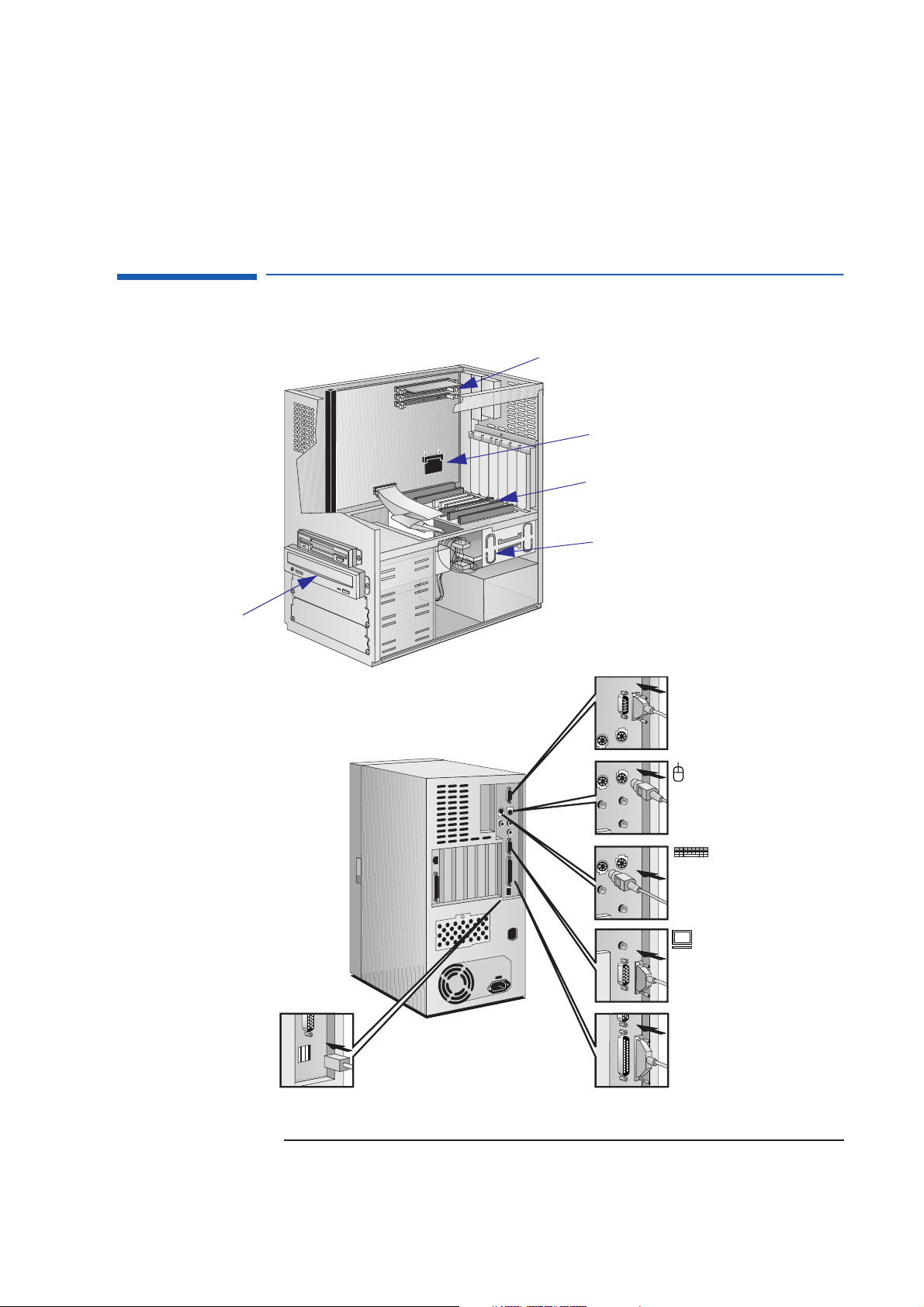
Front view
1 System Overview
Package for the Desktop Models
Package for the Desktop Models
(Multimedia models only)
Front view with
cover removed
Rear view
Four accessory
board slots
Video memory
Main memory
modules
Hard disk drive
(below power
supply unit)
24X CD-ROM drive
Flexible disk drive
(All icons
shown here are
for information, and do not
necessarily
appear on the
PC).
12
USB Serial APar al lel
KeyboardDisplay
Mouse
Page 13
Front view with
cover removed
Package for the Minitower Models
Main memory Modules
Video Memory Upgrade
Six accessory board slots
Hard disk drive
1 System Overview
Package for the Minitower Models
Rear view
24X CD-ROM drive
USB
Serial
Mouse
Keyboard
Display
Par al le l
(All icons shown here are for
information, and do not necessarily appear on the PC).
13
Page 14

1 System Overview
HP Kayak XA PC Workstation Overview
HP Kayak XA PC Workstation Overview
Component Desktop Minitower
Microprocessor
Main memory
Graphics controller
Communications
Mass storage
Accessory board slots
SCSI connectors
(SCSI models only)
Audio
CD-ROM drive
Flexible disk drive
Power supply
233, 266 or 300 MHz Pentium II MMX processor with 512 KB cache memory
Three DIMM sockets using:
32 MB, 64 MB or 128 MB ECC SDRAM to a maximum of 384 MB, or
16 MB, 32 MB, or 64 MB non-ECC SDRAM to a maximum of 192 MB
Integrated AGP video controller with 2 MB of built-in video memory and 2 MB of removable video memory
(Rev. A).
Or, an on-board 4 MB (soldered onto the system board) video module (Rev B).
2 USB connectors, 1 serial port, 1 parallel port
2.5 GB IDE, or 2.1 or 4.5 GB SCSI
5 shelves (3 front-access, 2 internal
5 slots
2
(1 ISA, 2 PCI
, 2 combination ISA/PCI)
1
)
2.5 or 4.3 GB IDE, or 4.5 GB SCSI
6 shelves (4 front access, 2 internal)
6 slots
(2 ISA, 2 PCI, 2 combination ISA/PCI)
Ultra-wide internal SCSI connector and Ultra-narrow external SCSI connector
Integrated 16-bit hi-fi audio processor with music synthesizer and mixer
24X speed IDE CD-ROM on all models
New version without bezel New version without bezel
Input voltage: 100-127, 200-240V ~
Input frequency: 50/60Hz
Maximum output power: 120W continuous
Input voltage: 100-127, 200-240V ~
Input frequency: 50/60Hz
Maximum output power: 160W continuous
On (idle - no file transfer) - Windows 95: 32W (115V/60Hz), 35W (230V/50Hz)
Power saving
On (idle - no file transfer) - Windows NT 4.0: 45W (115V/60Hz), 45W (230V/50Hz)
Sleep/Suspend mode - Windows 95: 25.5W (115V/60Hz), 29W (230V/50Hz)
Off: 1.6W (115V/60Hz), 3W (230V/50Hz)
1.
Models with a LAN or LAN/SCSI board only have one internal mass storage shelf.
2.
Models with a LAN or LAN/SCSI board only have one PCI slot.
14
Page 15

Desktop Hardware
Control Panel
Power On Status Light
Hardware Control Panel
Hard Disk Activity
Light
Network Activity
Light
PC Lock Activity
Light
1 System Overview
Hardware Control Panel
Reset
Button
Power On/Off Button
Volume Control Speaker Out for Headset
Minitower Hardware
Control Panel
Power On/Off Button
Power on Status
Light
Hard Disk Activity
Light
Microphone connector
Network Activity
Light
PC Lock Button
PC Lock Activity
Light
Reset Button
PC Lock Button
Volume Control
Speaker Out for Headset
Microphone connector
15
Page 16
1 System Overview
Specifications and Characteristic Data
Specifications and Characteristic Data
Physical Characteristics
Desktop Characteristic Description
Weight
(excluding display and keyboard)
Dimensions Width: 43.5 cm (17.1 inches)
Footprint 0.194 m
Keyboard 18 inches (W) by 7 inches (D) by 1.3 inches (H), when flat, or
Minitower Characteristic Description
Weight
(excluding display and keyboard)
Dimensions Width: 19.2 cm (7.56 inches)
Footprint 0.085 m
Keyboard 18 inches (W) by 7 inches (D) by 1.3 inches (H), when flat, or
9 kg (20 pounds)
Height: 13.2 cm (5.2 inches)
Depth: 44.6 cm (17.5 inches)
2
(2.08 ft2)
18 inches (W) by 7 inches (D) by 2 inches (H), when standing
15 kg (33 pounds)
Height: 43.8 cm (17.24 inches)
Depth: 44 cm (17.32 inches)
2
(0.91 ft2)
18 inches (W) by 7 inches (D) by 2 inches (H), when standing
Electrical Specifications
Desktop Parameter Total Rating Notes
Typical per
PCI
Accessory
Slot
Typical per
ISA
Accessory
Slot
Input voltage 100-127
Vac
Power 120 W
Voltage range 90 to 264 VAC
Frequency range 45 Hz to 66 Hz
Input Surge Current Protection Maximum of 90A
Safety Ground Leakage Current > 3.5mA
16
200-240
Vac
Selected
automatically
1
Page 17

1 System Overview
Specifications and Characteristic Data
Desktop Parameter Total Rating Notes
Efficiency 70% at maximum power output
Output Voltage Regulation Min Nom Max
11.0 12.0 13.0
4.8 5.0 5.25
3.15 3.3 3.6
-4.5 -5.0 -5.5
-10.8 -12.0 -13.2
4.7 5.0 5.3 (5 VStd By)
Overvoltage Protection Not more than 6.5V for 5V output
Not more than 16V for 12V output
Isolation Voltage 3000Vac primary/secondary
1500Vac primary/ground
Safety Standard IEC950/UL 1950/CSA950/EN60950
Typical per
PCI
Accessory
Slot
Typical per
ISA
Accessory
Slot
Maximum input current 3 A
Current at +5 V 14 A 2.5 A 1 A
Current at +3.3 V 8 A
Total cumulated current on
20 A ——
+3.3 V and +5 V
Current at -5 V 0.1 A — 0.2 A
Current at +5V standby 0.3 A
Current at +12 V 4 A 0.2 A 0.2 A
Current at -12 V 0.3 A 0.2 A 0.5 A
Minitower Parameter Total Rating Notes
Input voltage 100-127
Vac
200-240
Vac
Manual Switch
Typical per
2
——
— 0.2 A
Typical per
PCI
Accessory
Slot
ISA
Accessory
Slot
17
Page 18

1 System Overview
Specifications and Characteristic Data
Desktop Parameter Total Rating Notes
Power 160 W
(200 W peak)
Voltage range 90-140
Vac
180-264
Vac
Frequency range 45 Hz to 66 Hz
Maximum input current 5 A
Input Surge Current Protection Maximum of 90A
Safety Ground Leakage Current > 3.5mA
Efficiency 75% at maximum power output
Output Voltage Regulation Min Nom Max
11.0 12.0 13.0
4.8 5.0 5.25
3.15 3.3 3.6
-4.5 -5.0 -5.5
Typical per
PCI
Accessory
Slot
Typical per
ISA
Accessory
Slot
-10.8 -12.0 -13.2
4.7 5.0 5.3 (5 VStd By)
Overvoltage Protection Not more than 6.5V for 5V output
Not more than 16V for 12V output
Isolation Voltage 3000Vac primary/secondary
1500Vac primary/ground
Safety Standard IEC950/UL 1950/CSA950/EN60950
Output Voltage Regulation Min Nom Max
Current at +5 V 20 A 2.5 A 1 A
Current at +3.3 V 12 A
Total cumulated current on
20 A —
—
+3.3 V and +5 V
Current at -5 V 0.2 A — 0.2 A
Current at +5V standby 0.3 A
— 1 A
18
Page 19

1 System Overview
Specifications and Characteristic Data
Desktop Parameter Total Rating Notes
Current at +12 V 4.4 A
Current at -12 V 0.5 A
1.
Note that even though the desktop power supply is autoselect, it is not a full range power supply.
It works in 2 input voltage range and not in one big 90 V to 240 V range.
2.
On minitower models, always check the voltage switch position at first power-on.
— 0.2 A 0.2 A
— 0.2 A 0.5 A
An attempt to draw too much current (such as a short circuit across edgeconnector pins, or an accessory board that is not suitable for these PC
Workstations), will cause the overload protection in the power supply to be
triggered, and the PC Workstation could fail to boot.
Both power supplied on the desktop and minitower models are new
compare to the ones used on previous platforms (Vectra VL 6/xxx and XA 6/
xxx). The difference is at the V standby level, which has been extended to
deliver 300mA instead of 100mA. This extra current is required by the
100TX hardware layer so it can perform a remote power-on at reception of a
magic frame. Using an older power supply for a repair will prevent a remote
power-on at reception of a magic frame.
Typical per
PCI
Accessory
Slot
Typical per
ISA
Accessory
Slot
NOTE When the PC Workstation is turned off with the power button on the front
panel, the power consumption falls below 5 Watts, but is not zero. The special
on/off method used by this PC Workstation extends the lifetime of the power
supply. To reach zero power consumption in “off” mode, either unplug the PC
Workstation from the power outlet or use a power block with a switch. You
should be aware that the PC Workstation will lose its time settings within a
few days if you unplug the PC, or switch off the PC Workstation at the power
block.
19
Page 20

1 System Overview
Specifications and Characteristic Data
Environmental Specifications (Desktop and Minitower)
Environmental Specifications (System Processing Unit, with Hard Disk)
Operating Temperature +5°C to +40°C (+ 40°F to 104° F)
Recommended Operating
Temperature
Storage Temperature -40°F to +158°F (-40°C to +70°C)
Over Temperature Shutdown +50°C (+122°F)
Operating Humidity 15% to 80% (relative)
Storage Humidity 8% to 80% (relative)
Acoustic noise emission:
Sound power
Sound pressure
Operating Altitude 10000 ft (3100m) max
Storage Altitude 15000ft (4600m) max
+15°C to +70°C (+59°F to +158°F)
(as defined ISO 7779)
LwA ≤ 42 db
LpA ≤ 37 db
Operating temperature and humidity ranges may vary depending upon the
mass storage devices installed. High humidity levels can cause improper
operation of disk drives. Low humidity levels can aggravate static electricity
problems and cause excessive wear of the disk surface.
20
Page 21

1 System Overview
Documentation
Documentation
The table below summarizes the availability of documentation that is
appropriate to the HP Kayak XA PC Workstations.
Only selected publications are available on paper. Most are available as
viewable files (which can also be printed) from the HP division support
servers, and on the HP Support Assistant CD-ROM.
Division Support
Server
(where available)
HP Kayak XA PC Workstation User’s
Guide
HP Kayak XA PC Workstation
Familiarization Guide (D4790-90901)
HP Kayak XA PC Workstation
Technical Reference Manual
HP Kayak XA PC Workstation Service
Handbook (1st Edition)
Network Administrators Guide WinHelp, HTML and
HP 10/100BT NightDIRECTOR/10
Ethernet Card Installation Guide
(D3998-90001)
PDF file PDF file
PDF file PDF file no
PDF file PDF file no
PDF file PDF file
text formats
PDF file PDF file no
Online at HP
WWW Site
(see address
below)
PDF file no
Paper-based
DT: D4790A
MT: D4800A
5966-8261
Each PDF file (Portable Document Format) can be viewed on the screen by
opening the file with Acrobat Reader. To print the document, press Ctrl+P
whilst you have the document on the screen. You can use the page-up, pagedown, goto page, search string functions to read the document on the
screen.
Access HP World Wide
Web
Additional online support documentation, BIOS upgrades and drivers are
available from HP’s World Wide Web site, at the following address:
World-Wide Web URL:
http://www.hp.com/go/kayaksupport
21
Page 22

1 System Overview
Documentation
Where to Find the Information
The following table summarizes the availability of information within the HP
Kayak XA PC Workstation documentation set.
Product features
Product model
numbers
Connecting cables and
turning on
Finding on-line
information
Environmental
Formal documents
Opening the computer
Supported
accessories
Replacing accessories
Configuring devices
Fields and their
options within Setup
User Guide User Online
Introducing the computer
Key features Key features
Using the computer
Keyboard, mouse, display,
network, printer, power
Finding READ.MEs and
on-line documentation
Setting Up and Using Your
PC Workstation
Software license
agreement
Warranty information
Full details New procedures
Some part number details Full PN details Full PN details
How to install New procedures
Installing drivers Configuring the HP
Key fields Key fields
Configuring your
Web Browser
Working in
comfort
S/w license
agreement
Upgrading the computer
Enhanced
Keyboard
1
Familiarization
Guide
New features Exploded view
Service
Handbook
Parts list
Product range
CPL dates
Technical
Reference
Manual
Key features
System overview
Troubleshooting
Technical information
Repairing the computer
Basic Repair policy Service notes Advanced
Basic Detailed Advanced
22
Page 23

1 System Overview
Documentation
System board
BIOS
Power-On Self-Test
routines (POST)
Audio User’s Guide
LAN Administrator’s
Guide
1.
For the address, refer to “Access HP World Wide Web” on page 21.
Technical
Reference
Manual
Jumpers, switches
and connectors
Chip-set details
User Guide User Online
Jumpers, switches and
connectors
Familiarization
Guide
Jumpers, switches
and connectors
How to replace
Service
Handbook
Jumpers,
switches and
connectors
Basic details Upgrading Technical details
Memory maps
Key error codes and
suggestions for corrective
action
Error codes and
suggestions for
corrective action
Order of tests
Complete list
Peripheral Devices
Setting up and configuring Setting up,
configuring and
troubleshooting
Setting up and configuring Setting up and
configuring
23
Page 24

1 System Overview
Documentation
24
Page 25

2
System Board
This chapter describes the components of the system board, taking in turn
the components of the Processor-Local Bus, the Peripheral Component
Interconnect (PCI) bus, the System Management (SM) bus and the Industry
Standard Architecture (ISA) bus and the AGP Accelerated Graphics Port
Controller.
25
Page 26

2 System Board
System Board and Backplane Boards
System Board and Backplane Boards
Both desktop and minitower models have an AGP graphics controller built
into the system board.
1
. Also includes: SCSI Led and external SCSI cable detection.
26
1
Page 27

2 System Board
System Board and Backplane Boards
Desktop
Backplane
(front view)
Desktop
Backplane
(rear view)
Slot 1(the top slot). Can be used for a
32-bit PCI board).
Slot 2. Can be used for a 32-bit PCI or
a 16-bit ISA board (maximum length
17-cm/6.7-inches).
Slot 3. Can be used for either a full-
length 32-bit PCI or a full-length 16bit ISA board.
Slot 4 (the bottom slot). Can be used
for a full-length 16-bit ISA board.
System board slot.
Slot 5 (the supplementary slot) is under
the power supply unit. There is probably
already a LAN board or a SCSI/LAN
board installed in this slot. This slot can
be used for a 32-bit PCI board (maximum length 16-cm/6.3-inch).
J12
J6
J10
J7
Desktop Backplane PCI Mapping Table
Device
0 11 440LX PAC
4 15 PIIX4
12 23 J12 3
617J62
10 21 J10 1
7 18 J7 Rear of Backplane
11 22 (not used)
#AD[xx] PCI Device Slot#
Board
27
Page 28

Minitower
Backplane
(top view)
2 System Board
System Board and Backplane Boards
Slots 5 and 6. These slots can be used
for full-length 16-bit ISA boards.
Slot 4. These slots can be used for a
16-bit ISA or a 32-bit PCI board.
Slots 2 and 3. Can be used for 32-bit
PCI boards.The maximum length for a
board in slot 2 is 17-cm/6.7 inches.
Slot 1. Can be used for a 16-bit ISA or
a 32-bit PCI board (17-cm/6.7 inch
maximum length).
System board slot.
Minitower Backplane PCI Mapping Table
Device
0 11 440LX PAC
4 15 PIIX4
12 23 J12 4
617J63
#AD[xx] PCI Device Slot#
J12
J6
J2
J1
10 21 J10 2
718J71
11 22 (not used)
28
Page 29

Architectural View
2 System Board
Architectural View
Intel Pentium II Processor
Address (32)
Control
Data (64)
PCI Bus
(32 bit, 33 MHz)
Cirrus
AGP
CL5465
IDE
USB
USB
440 LX PAC
82443LX
PCI/ISA Bridge (PIIX4)
82371AB
Interrupt
Controller
PCI Bus
Interface
SMBus
Controller
Ultra DMA
Controller
ISA Bus
Interface
Memory Bus
72-bit ECC
Processor-Local
(GTL) Bus (64 bit,
66 MHz)
Main Memory
3 DIMMS
(Serial Presence
Detect)
PCI Slots
Clock
Clock
SMBUS
LM75
LAN/SCSI
CK4D
PLL
Serial
EEPROM
ISA Slots
ISA Bus
(16 bit, 8.25MHz)
29F002T Flash
EEPROM
Little Ben
Super I/O
NS82317
AD-1816
Aud io
29
Page 30

2 System Board
Chip-Set
Chip-Set
The Intel AGPset is comprised of two chips. The 440LX PAC chip and the
PIIX4chip.
• The PAC chip (440LX) is the bridge between four buses: the PL (GTL)
bus, the main memory bus, the PCI bus and the AGP (graphic) bus.
• The PIIX4 chip is the bridge between three buses: the PCI bus, the SM bus
and the ISA bus. In addition, it contains the IDE controller, USB
controller and Power Management logic
The PAC Chip (440LX)
The PAC chip, called the Intel 440LX AGPset, is contained in a Ball Grid
Array (BGA) package, giving a smaller footprint and higher reliability.
The PAC chip integrates a Host-to-PCI bridge, optimized DRAM controller
and data path, and an Accelerated Graphics Port (AGP) interface. The AGP
is a high performance, component level interconnect, targeted at 3D
graphics applications.
PL Bus Interface The PAC chip monitors each cycle that is initiated by the processor, and
forwards those to the PCI bus that are not targeted at the local memory. It
translates PL bus cycles into PCI bus cycles.
The chip can support one or two Pentium II processors, at up to 66 MHz FSB
clock frequency. Refer to page 35
Processor-Local Bus.
for a description of the devices on the
PCI Bus Interface The PCI bus interface is PCI 2.1 compliant.
Sequential PL-to-PCI memory write cycles are translated into PCI zero wait
state burst cycles. The maximum PCI burst transfer can be between
256 bytes and 4 KB. The chip supports advanced snooping for PCI master
bursting, and provides a pre-fetch mechanism dedicated for IDE read.
The PCI arbiter supports PCI bus arbitration for up to six masters using a
rotating priority mechanism. Its hidden arbitration scheme minimizes
arbitration overhead. Additional logic on the PC Workstation extends the
number of fully supported masters to seven (440LX master not counted).
Refer to page 39
30
for a description of the devices on the Processor-Local Bus.
Page 31

2 System Board
Chip-Set
AGP Bus Interface A controller for the AGP (Accelerated Graphics Port) slot is integrated in the
440LX PAC chip. The PAC chip supports only a synchronous AGP interface,
coupling to the host bus frequency. The AGP characteristics are described in
detail in “Accelerated Graphics Port (AGP) Controller” on page 41
.
Main Memory Controller The main memory controller supports three DIMM slots. Each slot can host
a 168-pin unbuffered SDRAM module, running at 66MHz, for a total of up to
348 MB of dynamic random access memory (ECC SDRAM).
The memory bus is 72-bits wide, comprised of 64 bits of data and 8 bits of
ECC. Refer to “Main Memory Bus” on page 38
memory.
, for more detail on the main
Read/Write Buffers The PAC chip defines a data buffering scheme to support the required level
of concurrent operations and provide adequate sustained bandwidth
between the DRAM subsystem and all other system interfaces (CPU, AGP
and PCI).
System Clocking The PAC chip operates the host interface at 66MHz, PCI at 33 MHz and AGP
at 66/133 MHz. Coupling between all interfaces and internal logic is done in a
synchronous manner. The PAC chip is not designed to support host bus
frequencies lower than 66 MHz. The clocking scheme uses an external clock
synthesizer (which produces reference clocks for the host, AGP and PCI
interfaces).
31
Page 32

2 System Board
Chip-Set
The PIIX4, PCI/ISA Bridge Chip (82371AB)
The universal host controller interface (UHCI) chip, known as PIIX4, is
encapsulated in a Ball Grid Array (BGA) package.
The PIIX4 chip is a multi-function PCI device implementing a PCI-to-ISA
bridge function, a PCI IDE function, a Universal Bus host/hub function, and
an Enhanced Power Management function.
The following figure shows an example of the system block diagram using
the PIIX4 chip.
Host Bus
Cirrus AGP
CL5465
PCI Bus (3.3V or 5V, 30/33 MHz)
Hard Disk
Hard Disk
Second Level
Cache
BMI IDE
Ultra DMA/33
AGP Bus
PCI/ISA Bridge (PIIX4)
Processor
Host-to-PCI
82371AB
Bridge
Memory Bus
Main Memory
USB 1
USB2
GP[I,O] (30+)
DRAM
PCI Slots
CD-ROM
ISA/EIO Bus (3.3V; 5V Tolerant)
32
SM Bus
Audi o
KBD
SP, PP,
FDC, IR
BIOS
Page 33

2 System Board
Chip-Set
PCI Bus Interface This part of the chip is responsible for transferring data between the PCI bus
and the ISA expansion bus. It performs PCI-to-ISA, and ISA-to-PCI bus cycle
translation. It supports the Plug-and-Play mechanism. Data buffers are
provided, to isolate the PCI and ISA buses. Refer to page 39
of the devices on the PCI Bus.
for a description
ISA Bus Interface As well as accepting cycles from the PCI bus interface, and translating them
for the ISA bus, the ISA bus interface also requests the PCI master bridge to
generate PCI cycles on behalf of a DMA or ISA master. The ISA bus interface
contains a standard ISA bus controller and data buffering logic. It can
directly support six ISA slots without external data or address buffering.
Refer to page 45
for a description of the devices on the ISABus.
SMBus Controller The System Management (SM) bus is a two-wire serial bus provided by the
PIIX4 controller. It runs at a maximum of 16 kHz. The bus monitors some of
the hardware functions of the main board, both during boot-up and run-time.
All accesses to the SM bus are handled by the main processor, via the PIIX4
SM bus registers. Refer to page 43
(System Management) Bus.
for a description of the devices on the SM
IDE Controller The PCI master/slave IDE controller, supporting four devices, two on each of
two channels, is described on page 39
.
USB Controller The PCI USB (Universal Serial Bus) controller, supports two stacked USB
connectors on the back panel. These ports are built into the PIIX4
controller, as standard USB ports. The USB is described in detail on page 40
Ultra DMA Controller The seven channel DMA controller incorporates the functionality of two
82C37 DMA controllers. Channels 0 to 3 are for 8-bit DMA devices, while
channels 5 to 7 are for 16-bit devices (see page 82
programmed for any of the four transfer modes: the three active modes
(single, demand, block), can perform three different types of transfer: read,
write and verify. The address generation circuitry supports a 24-bit address
for DMA devices.
). The channels can be
Interrupt Controller The interrupt controller incorporates the functionality of two 82C59
interrupt controllers. The two controllers are cascaded, supporting 15
interrupts (edge/level triggered). A table on page 83
shows how the master
33
.
Page 34

2 System Board
Chip-Set
and slave controllers are connected.
Counter / Timer The chip contains a three-channel 82C54 counter/timer. The counters use a
division of the 14.318 MHz OSC input as the clock source.
Serial EEPROM This is the non-volatile memory which holds the values for the Setup
program (they are no longer stored in the CMOS memory). The Serial
EEPROM is described on page 43
.
Cache Memory
There are two integrated circuits sealed within a single Pentium II package.
One of these contains the Level-2 (L2) cache memory chip; the other
contains the processor, which itself includes two banks of Level-1 (L1)
cache memory.
The L1 cache memory has a total capacity of 32KB (16 KB data, 16 KB
instruction). The L2 cache memory has a capacity 512 KB, and is composed
of four-way set-associative static RAM. Data is stored in lines of 32-bytes
(256 bits). Thus two consecutive 128-bit transfers with the main memory
are involved for each transaction.
The amount of cache memory is set by Intel at the time of manufacture, so
cannot be changed.
34
Page 35

2 System Board
Devices on the Processor-Local Bus
Devices on the Processor-Local Bus
The Processor-Local (PL) bus of the Pentium II processors, also referred to
as their FSB (Front Side Bus), is implemented in the GTL+ technology. This
technology features open-drain signal drivers that are pulled-up to 1.5 V
through 56 ohm resistors on both ends of the bus; these resistors also act as
bus terminators, and are integrated in the Pentium II processors.
The supported operating frequencies of the GTL+ bus are 60 MHz and
66 MHz. The width of the data bus is 64 bits, the width of the address is 32
bits.
The control signals of the PL bus allows the implementation of a “split -
transaction” bus protocol. This allows the Pentium II processor to send its
request (such as asking for the contents of a given memory address) and
then to release the bus, rather than waiting for the result, thereby allowing
to accept another request. The 440LX as target device then requests the bus
again when it is ready to respond, and sends the requested data packet. Up
to four transactions are allowed to be outstanding at any given time.
Intel Pentium II Microprocessor
The Pentium II processor has several high-performance features that
enhance performance:
• Dual Independent Bus architecture, which combines a dedicated 64-bit
L2 cache bus (supporting level cache sizes of 256K or 512K), plus a 64-bit
system bus with ECC that enables multiple simultaneous transactions (refer to above “split -transaction”).
• Intel MMX technology, which gives higher performance for media, communications and 3D applications.
• Dynamic execution to speed up software performance.
The Pentium II processor and level-2 cache memory are packaged in a selfcontained, pre-sealed module, installed in a socket on the system board.
35
Page 36

2 System Board
Devices on the Processor-Local Bus
The heat-sink is supplied with the processor, and is bolted to it by the
manufacturer. The module is held in place by a bracket. There are two
plastic clips, one on the top of each pillar of the bracket, to hold the
processor module in place.
To remove the old processor module:
1 Press the two plastic clips towards each other.
2 Carefully pull the processor module away from its connector on the
system board.
Only upgrades, pin compatible with the original processor, manufactured by
Intel, are supported.
Plastic clips
Bracket pillars
Heat sink
36
Page 37

2 System Board
Devices on the Processor-Local Bus
Bus Frequencies There is a 14.318 MHz crystal oscillator on the system board. This frequency
is multiplied to 66 MHz by a phase locked loop. This is further scaled by an
internal clock multiplier within the processor.
For example, the Pentium II 300 MHz processor multiplies the 66 MHz
system clock by 4.5. Switches 1 and 2, on the system board switches, set the
frequency of the Processor-Local bus, which for all HP Kayak XA PC
Workstation models, is 66 MHz. Switches 3, 4 and 5 set the clock multiplier
ratio.
Switch
Processor
Frequency
233 MHz
266 MHz Open Open 66 MHz 33 MHz 8.25 MHz Closed Open Open 4 : 1
300 MHz
333 MHz
1.
2.
system board repair is performed.
1 2 3 4 5
Open Open 66 MHz 33 MHz 8.25 MHz Open Closed Closed 3.5 : 1
Open Open 66 MHz 33 MHz 8.25 MHz Closed Open Closed 4.5 : 1
Open Open 66 MHz 33 MHz 8.25 MHz Closed Closed Open 5 : 1
Processor bus frequency is always set at 66MHz for all XA PC Workstations models.
Switches are provided to match the system board to processor frequency when a
Processor
Local Bus
Frequency
1
PCI Bus
Frequency
ISA Bus
Frequency
Switch
2
Frequency
Processor:
Local Bus
The computer may execute erratically, if at all, or may overheat, if it is
configured to operate at a higher processor speed than the processor is
capable of supporting. This can cause damage to the computer.
Setting the switches to operate at a slower speed, than the processor is
capable of supporting, can still cause erratic behavior in some cases, and
would reduce the instruction throughput in others.
Ratio
37
Page 38

2 System Board
Main Memory Bus
Main Memory Bus
The memory bus is 72-bits wide, comprised of 64 bits of data and 8 bits of
ECC. It is connected to the Main Memory and to the PAC (440LX) chip.
There are three 168-pin DIMM slots on the system board for installing main
memory; slots A, B and C. All HP Kayak XA PC Workstation models are
supplied with one memory module (either 16 MB, 32 MB or 64 MB ECC
SDRAM) in one of the three slots, leaving the other slots free for memory
upgrades.
The slots can be filled in any order, but there is a performance advantage in
filling the slots in the order A, B, C. Memory upgrades are available in single
32 MB, 64 MB or 128 MB ECC SDRAM modules. Note that replacement of
the supplied memory module may be necessary to obtain the 384 MB
maximum memory, unless the supplied module was 128 MB.
With non-ECC SDRAM memory modules, a maximum of 192 MB can be
obtained. These memory modules can be either; 16 MB, 32 MB or 64 MB.
NOTE If ECC and non-ECC memory modules are both installed, ECC will be
invalidated for all memory modules.
Error Correcting Code
Operation
The error correcting code (ECC) memory of the HP Kayak XA PC
Workstation allows any single bit error that occurs in any 72-bit line of
memory (64 data bits plus 8 parity bits) to be corrected (automatically and
transparently) by the PAC chip.
The ECC detects single and dual bit errors. It can correct single bit errors
during SDRAM reads. The corrected data is transmitted to the requester
(PCI or CPU) but not written back to the SDRAM. A double bit error would
cause an NMI to be generated, and the PC Workstation to be halted.
If more bits are faulty within any given 72-bit line, the effect is the same as it
would have been without error correction. The effect of executing a faulty
instruction is always unpredictable, and might cause the program to ‘hang’.
The effect of reading a faulty data word is often similarly unpredictable, but
can sometimes be tolerated (for instance, it might merely appear as a
corrupted pixel on a video display).
38
Page 39

Devices on the PCI Bus
2 System Board
Devices on the PCI Bus
PCI Device
PL/PCI bridge
Virtual PCI-to-PCI bridge (AGP)
PCI/ISA bridge
IDE controller
USB Host controller
Power Management and SM Bus
PCI slot #1 (LAN) - Minitower
Backplane Rear Board - Desktop
PCI slot #2 - Minitower 17 10 0-7 21 D A B C
PCI slot #1 - Desktop
PCI slot #3 - Minitower 18 6 0-7 17 C D A B
PCI slot #2 - Desktop
PCI slot #4 - Minitower 19 12 0-7 23 B C D A
PCI slot #3 - Desktop
Device
Name
440LX PAC 0 N/A 11 — — — —
440LX PAC 1 N/A 12 — — — —
PIIX4 4 0 15 — — — —
16 7 0-7 18 A B C D
Device
Number
Function AD[xx]
1 — — — —
2 — — — —
3 — — — —
Chip-set Interrupt Connection
INTA INTB INTC INTD
The distribution of the interrupt lines is described more fully on page 83.
Integrated Drive Electronics (IDE)
The IDE controller is implemented as part of the PIIX4 chip (the PCI/ISA
bridge). It is driven from the PCI bus, and has PCI-Master capability. It
supports Enhanced IDE (EIDE) and Standard IDE. To use the Enhanced
IDE features the drives must be compliant with Enhanced IDE.
The IDE controller supports two devices (one master and one slave)
connected to a single channel. The channel is fitted with an IDE cable with
two connectors.
39
Page 40

2 System Board
Devices on the PCI Bus
It is possible to mix a fast and a slow device, such as a hard disk drive and a
a CD-ROM, on the same channel without affecting the performance of the
fast device. The BIOS determines automatically, the fastest configuration
that each device supports. However, in general, the IDE cable is
recommended for CD-ROM drives, and the SCSI cables for hard disk drives.
Universal Serial Bus (USB) Controller
The USB controller is implemented as part of the PIIX4 chip. It is accessed
through the PCI bus, and provides support for the two stacked USB
connectors on the back panel. Over-current detection and protection is
provided, but shared between the two ports.
USB works only if the USB interface has been enabled within the HP Setup
program. Currently, only the Microsoft Windows 95 and Windows NT
operating systems provides support for the USB.
The Microsoft Supplement 2.1 software called (called
USBSupp.exe), which
provides support of the Universal Serial Bus, can be obtained from the
Hewlett-Packard World Wide Web site (refer to “Access HP World Wide
Web” on page 21).
Other PCI Accessory Devices
PCI accessory boards are for high-speed peripheral accessories. A network
board could already occupy one of the PCI slots. A diagram showing the PCI
slots that are available for the desktop and minitower models is on page 27
Plug and Play The HP Kayak XA/ PC Workstations have a “PnP level 1.0A” BIOS and
meets the “Windows 95 Required” level for Plug and Play. Accessory boards
which are Plug and Play are automatically configured by the BIOS.
.
40
Page 41

2 System Board
Accelerated Graphics Port (AGP) Controller
Accelerated Graphics Port (AGP) Controller
The AGP technology was developed as a means to access system memory as
a viable alternative to augmenting the memory of the graphics subsystem
needed for high quality 3D graphics applications. All models of HP Kayak
XA PC Workstations support an AGP (Accelerated Graphics Port) device
(Laguna Graphic Controller from Cirrus).
The AGP bus is based upon a 66 MHz, 32 Bit PCI bus architecture, to which
several signal groups have been added. These additional signals allow to
implement AGP specific control and transfer mechanisms, which are:
• Pipelining and sideband addressing. These control mechanisms increase the bus efficiency compared to the PCI protocol.
• Double clocking (2x mode). This is a transfer mechanism that doubles
the peak transfer rate to 528 MB/s, as two 32 Bit words are transferred in
each clock period (2 x 32
bits x 66 MHz).
AGP specific transactions always use pipelining. The other two mechanisms
can combine independently to pipelining, which leads to these operating
modes:
• FRAME based AGP. Only the PCI protocol is used: 66 MHz, 32 Bits, 3.3V,
264 MB/s peak transfer rate.
• 1 X AGP with pipelining, sideband addressing can be added: 66 MHz, 32
Bits, 3.3V, increased bus efficiency, 264 MB/s peak transfer rate.
• 2 X AGP with Pipelining, sideband addressing can be added: 66 MHz double clocked, 32 Bits, 3.3V, increased bus efficiency, 528 MB/s peak transfer rate.
41
Page 42

2 System Board
Accelerated Graphics Port (AGP) Controller
AGP PCI Bus
Implementation
In the below diagram, the AGP Bus is viewed as a PCI bus with extra data
lines.
Pentium II Processor
66 MHz
AGP
Device
PCI Bus # 1
LX-Device 1
AGP Port
Virtual PCI-PCI Bridge
33 MHz
440 LX - Device 0
Host to PCI Bridge
PCI Bus # 0
PCI/ISA Bridge (PIIX4)
42
Page 43

Devices on the SM Bus
Device SM Bus Address
PIIX4 SM Bus Master 10
Serial EEPROM A8, AA, AC, AE
LM75 90
SDRAM slot 1 A0
SDRAM slot 2 A2
SDRAM slot 3 A4
2 System Board
Devices on the SM Bus
PLL D2
The System Management (SM) bus is used to monitor several of the
hardware functions (such as voltage levels, temperature, fan speed, DIMM
presence and type) of the system board. It is controlled by the SM bus
controller located in the PIIX4 chip.
Serial EEPROM
This is the non-volatile memory which holds the default values for the CMOS
memory (in the event of battery failure).
When installing a new system board, the Serial EEPROM will have a blank
serial number field. This will be detected automatically by the BIOS, which
will then prompt the user for the serial number which is printed on the
identification label on the back of the PC Workstation.
The computer uses 4 Kbit of Serial EEPROM implemented within a single
512 K ✕ 8-bit ROM chip. Serial EEPROM is ROM in which one byte at a time
can be returned to its unprogrammed state by the application of appropriate
electrical signals. In effect, it can be made to behave like very slow, nonvolatile RAM. It is used for storing the tatoo string, the serial number, and
the parameter settings for the Setup program.
43
Page 44

2 System Board
Devices on the SM Bus
LM75 Chip
The LM75 chip is a temperature sensor and alarm located on the system
board. It is used to measure the temperature in one area of the PC
Workstation, and to send an alarm to the processor in case of overheating.
This chip includes a security mechanism which prevents the system fan
from being disabled using software controls so long as the temperature
measured by the sensor is above the maximum operating temperature.
Main PLL
The registers of the main PLL are accessed through the SM bus. These
registers control the PLL clock signal outputs and are write-only.
WARNING: Writing over the SM bus may be destructive to the PC Workstation, as it
allows to access information necessary to the System BIOS, without which
the system will not run.
44
Page 45

Devices on the ISA Bus
ISA Device Index Data
2 System Board
Devices on the ISA Bus
Ultra I/O
Little Ben (HP ASIC)
2Eh 2Fh
96h 97h
The Super I/O Controller (NS 82317)
The Ultra I/O chip (NS 82317) provides the control for two FDD devices,
one serial port and one bidirectional multi-mode parallel port.
Serial / parallel
communications ports
The 9-pin serial port (whose pin layouts are depicted on page 71) supports
RS-232-C and are buffered by 16550A UARTs, with 16 Byte FIFOs. They can
be programmed as COM1, COM2, COM3, COM4, or disabled.
The 25-pin parallel port (also depicted on page 71
compatible, supporting IEEE 1284. It can be programmed as LPT1, LPT2, or
disabled. It can operate in the following four modes:
❒ Standard mode (PC/XT, PC/AT, and PS/2 compatible).
❒ Bidirectional mode (PC/XT, PC/AT, and PS/2 compatible).
❒ Enhanced mode (enhanced parallel port, EPP, compatible).
❒ High speed mode (MS/HP extended capabilities port, ECP, compatible).
) is Centronics
FDC The integrated flexible disk controller (FDC) supports any combination of
two of the following: tape drives, 3.5-inch flexible disk drives, 5.25-inch
flexible disk drives. It is software and register compatible with the 82077AA,
and 100% IBM compatible. It has an A and B drive-swapping capability and a
non-burst DMA option.
RTC The real-time clock (RTC) is 146818A-compatible. With an accuracy of
20 ppm (parts per million). The configuration RAM is implemented as 256
bytes of CMOS memory.
Keyboard and Mouse
Controller
The computer has an 8042-based keyboard and mouse controller. The
connector pin layouts are shown on page 71
.
45
Page 46

2 System Board
Devices on the ISA Bus
Audio Controller
The HP Kayak XA PC Workstation has an audio chip (AD1816) integrated
on the system board. This single chip is a Plug and Play multimedia audio
subsystem for concurrently processing multiple digital streams of 16-bit
stereo audio.
Host Interface The AD1816 audio chip contains all necessary ISA bus logic on chip. This
logic includes address decoding for all onboards resources, control and signal
interpretation, DMA selection and control logic, IRQ selection and control
logic, and all interface configuration logic.
Audio Chip
Specifications
It is driven from the ISA bus, and has the following specification:
Feature: Description:
Digitized Sounds • 16-bit and 8-bit stereo sampling from 4 kHz to 55.2 kHz
• Programmable sample rates with 1 Hz resolution
• Hardware Full Duplex Conversion
• 16-bit software-based real-time audio compression/
decompression system
Music Synthesizer • Integrated OPL3 compatible music synthesizer
Mixer • AC’97 and MPC-3 audio mixer
• Input mixing sources: microphone, LINE In,
CD Audio, AUX Audio, and digitized sounds
• Output mixing of all audio sources to the LINE Out or
integrated PC Workstation speaker
• Multiple source recording and Left/Right channels
swapping or mixing
Line Input • Input impedance: 15 kohms
• Input range: 0 to 2 Vpp
Line Output • Stereo output of 5 mW per channel with headphone
speakers (impedance >600 ohms)
Audio Front Panel • Microphone input jack
• Stereo output jack
• Master volume control potentiometer
46
Page 47

2 System Board
Devices on the ISA Bus
Feature: Description:
Microphone Input • 20 dB gain preamplifier. The boost can be muted with
software
• 16-level programmable volume control
• Input impedance: 600 ohms
• Sensitivity: 30 mVpp to 200 mVpp
Stereo Out Jack • Impedance: 32 ohms
The headphones jack and the stereo-out (audio) jack can be used
interchangeably. The Windows 95 and Windows NT operating systems each
have integrated drivers (Directions III).
Flash EEPROM
The PC Workstation uses 256 KB of Flash EEPROM implemented using one
8-bit ROM chip. Flash EEPROM is ROM in which the whole memory can be
returned to its unprogrammed state by the application of appropriate
electrical signals to its pins. It can then be reprogrammed with the latest
upgrade firmware.
The System ROM contains: the LAN boot firmware, and the system BIOS
(including the boot code, the ISA and PCI initialization, the Setup program
and the Power-On Self-Test routines, video BIOS, plus their error
messages). These are summarized in Chapters 4 and 5.
The Flash EEPROMs on the HP Kayak XA PC Workstation implement a
bootblock feature which allows recovery from a failed attempt at updating
the System BIOS. The bootblock contains the minimum system BIOS
information necessary to reprogram the Flash EEPROM.
47
Page 48

2 System Board
Devices on the ISA Bus
System Board Switches
The first two of the system board switches set the frequency of the
Processor-Local bus, and the next three the ratio of processor-frequency to
Processor-Local-bus-frequency, as summarized on page 37
The next five switches set the configuration for the PC Workstation, as
summarized in the table below.
Switch Switch Function Default
.
1Open
2 - 5 -
6
Open
Closed
7
Open
Closed
8
Open
Closed
Reserved - Do not use (always set to Open).
Bus Frequencies (see the table on page 37
Retain or clear the CMOS configuration stored in serial EEPROM:
Do not clear CMOS.
Clear CMOS and reload default values in Setup.
Enable or disable User and System Administrator Passwords stored in
EEPROM:
Enable passwords.
Disable /Clear User and Administrator passwords.
Keyboard power-on:
Disable keyboard power on.
Enable keyboard power on.
Boot block:
).
Open
-
Open
Open
Closed
9
10 Open
48
Open
Closed
Idle. Normal operation
Recovery boot active. Enable crisis recovery.
Reserved = do not use Open
Open
Page 49
2 System Board
Devices on the ISA Bus
The following diagrams show the position of the system board switches on
the desktop and minitower models.
BIOS Update Crisis
Recovery Procedure
If, for example, during a BIOS update process, the procedure is interrupted
by a power failure, and the system does not start, then you can still recover
the situation of a destroyed system BIOS. However, it should be noted that
during the recovery procedure, there is no image on the screen, nor access
to the keyboard or mouse (only “vital” devices that are required to boot on
the floppy are initialized). Follow these steps to recover the BIOS:
1 Ensure that you have created a DOS-bootable diskette. This floppy dis-
kette contains all the recovery and system BIOS programming software
(phlash.exe, platform.bin and hblxxxyy.Ful). Include the flash command
in the autoexec.bat, for example: phlash /mode=3 HC1xyyzz.Ful
H = HP Professional PC
C = Kayak XA (Pentium II models)
1 = Kayak family
x = major revision
yy = minor revision
zz = language
2 Turn off the computer. Set Switch 9 to the Closed position.
3 Insert the DOS-bootable diskette.
49
Page 50

2 System Board
Devices on the ISA Bus
4 Power on the computer.
5 During the recovery process, short beeps are emitted. The recover
process is finished when there is a much longer beep (after approximately
1 to 2 minutes).
6 Power off the computer. Press the power ON/OFF button (for about 5
seconds), until the ON/OFF light switches off. Set the switch 9 to the
Open position.
Updating the system
ROM
The System ROM can be updated with the latest BIOS firmware. This can be
downloaded from HP’s World Wide Web site:
http://www.hp.com/go/kayaksupport
To download a BIOS upgrade, connect to the HP Web site and follow the onscreen instructions to download the flash utility programs (
AUTOEXEC.BAT and PHLASH.EXE), the BIOS file (HC11xx.FUL), and a file
called
pfmhd106.bin, onto a bootable diskette.
FLASH.BAT,
Before updating the System ROM, it is necessary to disable the “PSWRD”
switch on the system switches (SW-7), and to type in the System
Administrator’s Password when starting up the computer. The PCI and PnP
information is erased in the process.
Do not switch off the computer until the system BIOS update procedure has
completed, successfully or not, otherwise irrecoverable damage to the ROM
may be caused. While updating the flash ROM, the power supply switch and
the reset button are disabled to prevent accidental interruption of the flash
programming process.
Little Ben
Little Ben is an HP application specific integrated circuit (ASIC), designed
to be a companion to the Ultra I/O chip, that is connected between the chipset and the processor. It contains the following:
• BIOS timer
❒ hardware wired 50 ms long 880 Hz beep module.
❒ automatic blinker that feeds the LEDs module with a 1 Hz oscillator
signal.
• Security protection (access, flash and anti-virus protection)
❒ For 128, 256 or 512 KB Flash EEPROMs.
50
Page 51

2 System Board
Devices on the ISA Bus
❒ For the Ultra I/O space: the Serial EEPROM, serial port, parallel port
and mass storage drives (disable write on Flexible Disk Drive, disable
boot on any drive, disable use of any embedded drive)
• Advanced Power Management (APM) version 1.2
• Glue logic (such as programmable chip selects)
When the user requests a ShutDown from the operating system, the
environment is first cleared. Any request to turn off the PC Workstation,
from the control panel, or from the operating system, can only be granted if
the PC Workstation is not locked by Little Ben’s lock bit (otherwise the
power remains on, a red light is illuminated, and the buzzer is sounded).
Other ISA Accessory Devices
ISA accessory boards are for slow peripheral accessories. A diagram
showing the ISA slots that are available for the desktop and minitower
models is on page 27
.
Plug and Play All PCI accessory boards are Plug and Play, although not all ISA boards are.
Check the accessory board’s documentation if you are unsure.
In general, in a Plug and Play configuration, resources for an ISA board have
to be reserved first (using the Setup utility) and then you can plug in your
board.
The procedure for installing an ISA accessory board that is not Plug and
Play is described in the User’s Guide that is supplied with the PC
Workstation.
NOTE The Windows NT 4.0 operating system is not Plug and Play. Information
explained above is only applicable for Plug and Play operating systems (for
example, Windows 95).
51
Page 52

2 System Board
Devices on the ISA Bus
52
Page 53

3
Interface Devices and Mass-Storage Drives
This chapter describes the graphics, mass storage and audio devices which
are supplied with the computer. It also summarizes the pin connections on
the internal and external connectors.
53
Page 54

3 Interface Devices and Mass-Storage Drives
Cirrus 5465 Graphics Controller Chip
Cirrus 5465 Graphics Controller Chip
The HP Kayak XA PC Workstation Desktop and Minitower models are
supplied with a Cirrus 5465
system board (refer to the architectural view on page 29
This chip integrates the necessary hardware for a flexible multimedia
display system. Including an integrated palette DAC, clock generators,
Enhanced V-Port bus for easy expandability, glueless AGP/PCI host
interface, glueless Rambus channels, and a 64-bit graphics engine featuring
GUI acceleration hardware (such as BitBLT, color expansion, 3D engine, and
hardware cursor).
The Cirrus 5465 Graphics Controller Chip also offers advanced features
such as BitBLT and line accleration, a general-purpose I/O port for
expansion, front-end and back-end video playback scaling, and color-space
conversion for video applications.
graphics controller chip integrated on the
for its location).
The Cirrus 5465 Graphics Controller Chip uses one of two Rambus channels
providing 500 to 600 Mbytes/second of memory bandwidth, displaying truecolor images of up to 1024 x 768 resolution, and 256-color modes that can
reach a maximum of 1600 x 1200 resolution.
The Cirrus Logic AGP 5465, can be characterized as follows:
®
• 100% hardware- and BIOS-compatible with IBM
• 64-bit video memory access with 2 MB, 50 ns, EDO, video DRAM (this is
not upgradeable since it is already fitted to capacity).
• 24-bit pixel bus (video playback width).
• 24-bit fractional component of texel addressing.
• 4- and 8-bit indexed texture source to 16- and 24-bpp display modes.
• Acceleration for playback, continuous interpolation on X, continuous
interpolation on Y.
• Chroma keying for substitution of graphics on video.
• Color expansion for 8-, 16-, 24-, and 32-bpp modes.
• Color keying for substitution of video on graphics.
• Color key support.
VGA display standard.
• DDC 2B compliant.
54
Page 55

3 Interface Devices and Mass-Storage Drives
Cirrus 5465 Graphics Controller Chip
• Green power saving features.
• GUI acceleration width (in bits).
• Hardware acceleration of graphical user interface (GUI) operations
through a bit-block transfer mechanism.
• Hardware cursor.
• Integrated programmable, dual-clock synthesizer.
• Integrated triple 8-bit DAC.
• Integrated 24-bit, 135 MHz RAMDAC.
• Lighted and shaded textures with Gouraud ramp and transparent texture.
• Maximum pixel clock.
• Maximum memory clock.
• PCI Bus Master mode for 2D/3D display list instruction fetch (Processor
mode) and data fetch and store to system memory.
• Point and line draw support via polygon engine DDAs.
• Specular lighting.
• Standard and Enhanced Video Graphics Array (VGA) modes.
• Superior TV-like quality video performance: hardware video window; YUV
video support; color key, chroma key; X & Y interpolated zooming.
• Support for up to 4 MB, 50 ns EDO video DRAM (though space is only
provided on the system board for 2 MB).
• Support for Gouraud shading in 8-, 16-, and 24-bpp display modes.
• Texture map source from system memory or RDRAM.
• Three-operand BitBLT.
• Video Overlay Support.
• Video playback acceleration.
• X, Y interpolated scaling.
• YCrCb support.
• YUV-to-RGB conversion in stretch engine path, supports MPEG textures.
• Z-storage and retrieval from either system memory or RDRAM.
55
Page 56

3 Interface Devices and Mass-Storage Drives
Cirrus 5465 Graphics Controller Chip
Connectors
The Video Electronics Standards Association (VESA) defines a standard
video connector, variously known as the VESA feature connector,
auxiliary connector, or pass-through connector. The graphics controller
supports an input/output VESA feature connector. This connector (whose
pin names are listed in a table on page 71
) is integrated on the system board,
and is connected directly to the pixel data bus and the synchronization
signals.
Video Memory
The HP Kayak Workstation PCs are supplied with 4 MB of video memory
integrated on the system board (revision B). There is either, an on-board
4 MB video memory soldered onto the system board. Or, 2 MB of built-in
video memory (revision A) and a 2 MB video memory module installed in
the video memory upgrade socket, giving 4 MB in total.
The video RAM (also known as the frame buffer) is a local block of 50 ns
EDO DRAM for holding both the on-screen surface (reflecting what is
currently displayed on the screen), and the off-screen surface (video frame,
fonts, double buffer).
The following diagrams show the position of the video memory module on
the minitower and desktop computers.
The soldered video memory (revision B) is located in the same area on the
system board as the video memory module.
56
Page 57

3 Interface Devices and Mass-Storage Drives
Cirrus 5465 Graphics Controller Chip
Available Video Resolutions
The number of colors supported is limited by the graphics device and the
video memory. The resolution/color/refresh-rate combination is limited by a
combination of the display driver, the graphics device, and the video
memory. If the resolution/refresh-rate combination is set higher than the
display can support, you risk damaging the display.
The following table, lists the video resolutions that are embedded in the
system BIOS.
Resolution Minimum video memory required for these color scales Refresh rates
256 colors
(8 bits per
pixel)
640 ✕ 480
800 ✕ 600 2 MB 60, 75, 85 Hz
1024 ✕ 768
1280 ✕ 1024
1600 ✕ 1200 2 MB 4 MB Not Available i48, 60, 75, 85 Hz
1.
The display may not support the refresh rates shown here. Refer to the User’s Guide supplied with
the display for details of the refresh rates supported.
2 MB 4 MB Not Available i43, 60, 75, 85 Hz
64 K colors
hi-color
(16 bits per
pixel)
2 MB 4 MB i43, 60, 75, 85 Hz
16.7 M
colors
true-color
(24 bits per
pixel)
2 MB 60, 75, 85 Hz
16.7 M
colors
true-color
(32 bits per
pixel)
A complete list of available standard VGA and enhanced video modes are
shown in the Appendix on page 100
.
1
57
Page 58

3 Interface Devices and Mass-Storage Drives
SCSI / LAN Combo Board
SCSI / LAN Combo Board
Certain HP Kayak XA PC Workstations are supplied with an integrated
SCSI / 10BT/100TX LAN combo board. Because the SCSI / LAN combo
board includes two controllers, only one PCI slot is necessary for installing
this board. The PCI and SCSI controllers access the PCI bus through a PCI
bridge. The SCSI and PCI functionalities of the SYM8751SP are contained
within the Symbios Logic SYM5C875J PCI-SCSI I/O Processor chip.
The following hardware functional diagram shows the SCSI part of the SCSI/
LAN Combo board.
External connector (8 bits)
Ext. Device Ext. Device
To ExtStart Connector
SCSI LED
LED connector
(not loaded)
PCI Interface
Term. Power Term. Power
50-pins high density
Termination H
Osc.
40MHz
eeprom
24C16
2KBytes
Clock
Data
5V
Fuse 3A
Termination L
PCI Bus
SCSI Controller
SYM53C875
PCI Bus
Internal connector (16 bits)
68-pins high density
Int. Device
12V
VPP Translator
Flash Memory
28F020
64KBytes
The PCI interface operates as a 32-bit DMA bus master. The connection is
made through the edge connector. The signal definitions and pin numbers
conform to the PCI Local Bus Specification Revision 2.0 standard. The PCI
interface conforms to the PCI universal signaling environment for a 5 volt or
3.3 volt PCI bus.
58
Page 59

3 Interface Devices and Mass-Storage Drives
SCSI / LAN Combo Board
10BT/100TX PCI LAN
Connector
The LAN adapter supports the following two standards: 100 VG-AnyLAN,
100 Mbits per second over 4-pair, category-3, unshielded twisted pair
(UTP), voice grade (VG) cable (IEEE 802.12 standard for Ethernet);
10 BaseT, 10 Mbits per second, ISO 8802-3 (IEEE 802.3 standard). On the
rear panel there is one RJ-45 unshielded-twisted-pair (UTP) connector. The
10BT/100TX LAN Features on page 62
are also valid for the 10 BT/100 TX
PCI LAN controller.
SCSI Interface
The Symbios Logic SYM5C875J PCI-SCSI I/O Processor chip connects
directly the SCSI bus and generates timing and protocol in compliance with
the SCSI standard.
The SCSI interface operates as 16-bit, synchronous or asynchronous, singleended, and supports Ultra SCSI protocols and 16-bit arbitration. The
interface is made through two (and only two) of the connectors J2, J3 and
J4.
Connector Description Location
J2 Shielded 68-pin high density right-angle receptacle. Protrudes through the
rear panel bracket.
Ultra wide (16-bit) SCSI
connector
J3 68-pin high density right-angle receptacle. Internal connector at the
end of the board.
J4 External Start, SCSI Led and External SCSI cable
detection.
Internal connector at the
bottom right-hand-side of
the Combo card.
The Ultra wide 16-bit SCSI connector is for internal devices and has an
address range from 0 to 15, with the SCSI address 0 used by the first SCSI
hard disk drive and SCSI address 7 reserved for the integrated SCSI
controller (the default for wide and narrow SCSI devices).
Data is transferred at 40 MB per second on 16-bit wide, single-ended bus.
The controller is fitted with a 16-bit SCSI flat cable with five connectors,
plus a SCSI termination device; so a maximum of 4 internal wide-SCSI hard
drives are supported.
59
Page 60

3 Interface Devices and Mass-Storage Drives
SCSI / LAN Combo Board
By default, the internal SCSI bus is configured to run in Ultra-SCSI mode
(providing a maximum band-width of 40 MB/s. The user may configure the
SCSI system using the SCSI Configuration Utility, included in the system
BIOS. This utility is described in more detail on page 77
.
SCSI-configured-automatically (SCAM) support is provided at level 2, for
Plug and Play. However, hot swap is not supported. The controller is BBS
compliant.
External (8-bit) SCSI
connector
The Ultra narrow 8-bit SCSI connector uses addresses ranging from 0 to 7. As
with the 16-bit internal SCSI connector, the SCSI address 0 is used by the first
SCSI hard disk drive and SCSI address 7 is reserved for the integrated SCSI
controller (the default for wide and narrow SCSI devices).
SCSI / PCI LAN Combo Board Features
Interface Features
PCI Interface
SCSI Interface 16-bit single ended.
Full 32-bit DMA bus master.
Zero wait-state bus master data bursts.
Universal PCI bus voltage support.
Automatically enabled active termination
Fast and Ultra SCSI data transfer capability.
SCSI TERMPWR source with auto-resetting circuit breaker
SCAM (SCSI Configured AutoMatically).
Serial NVRAM (Non-Volatile RAM) for configuration utility and SCAM.
60
Flash BIOS.
Fast and Ultra SCSI controlled by external SCSI cable detection.
Ultra speed requires 1.5m maximum SCSI bus.
Page 61

3 Interface Devices and Mass-Storage Drives
10BT/100TX LAN Controller
10BT/100TX LAN Controller
Certain models of the HP Kayak XA PC Workstation are supplied only with
a 10BT/100TX LAN adapter which supports the following standards:
100 Mbits per second over 2-pair, category-5, unshielded twisted pair
(UTP), or shielded twisted pair (STP); 10 BaseT, 10 Mbits per second, ISO
8802-3 (IEEE 802.3 standard).
On the rear panel there is one RJ-45 connector. There is an LED which
indicates the LAN connection status as follows:
• Off - when there is no Autonegotiation response (for example, when the
LAN cable is not connected to the network HUB.
• Blinking - during Autonegotiation
• Green (ON) - the connection has passed the Autonegotiation and a link
has been established between the LAN adapter and the network HUB/
Switch.
The LAN adapter contains a connector to which an internal LAN cable may
be connected to the external start connector on the system board, necessary
for the use of the Remote Power On feature, described in detail in the User’s
Guide provided with the PC Workstation. The LAN adapter that uses the
Remote Power On feature must be installed nearer the processors than any
other supplementary LAN adapter card.
Internal LAN connector for External
Start (Remote On)
LAN cable connector (RJ-45)
Optional ROM Socket
NOTE Refer to the User’s Guide for details concerning system configuration
changes necessary after installing a LAN adapter.
61
Page 62

3 Interface Devices and Mass-Storage Drives
10BT/100TX LAN Controller
10BT/100TX LAN Features
Feature: Description:
LAN Controller AMD PCNET-Fast chip
RJ45 Connector 10BT/100TX autonegotiation
Remote Boot Protocols integrated in System BIOS
ExtStart Connector • Connection to CPU board
• LAN remote power on signals
Remote Power On • Full remote power on with Magic Packet
Remote Wake Up • Wake Up from Suspend state with Magic Packet
Remote Power On
Remote Power On (RPO) is available at 10 and 100 Mbits per second.
Vstandby requirements
supporting RPO
The Vstandby requirements for HP network cards supporting RPO, is:
• A power supply able to deliver at least 250mA on Vstandby output. This is
the case for all HP Kayak systems.
Optional Bootrom Socket It is possible to add a flash device on the network card socket with a specific
LAN bootrom code. This new bootrom code will be seen and mapped
automatically by the system BIOS instead of the embedded version (system
BIOS).
NOTE At the time this TRM was produced, there was no flashing tool available to
allow you to update the bootrom content in the flash on the LAN adapter. A
flashing tool for any AMD based card may be available, but in order to use this
tool on HP cards, only 29fxxx flash devices must be used. At present, no test
has been carried out using this tool on HP cards.
Flash / ROM Devices The 10BT/100TX card provides a PLCC 32-pin socket and any size of flash
device can be used up to 256KB§.
62
Page 63

3 Interface Devices and Mass-Storage Drives
10BT/100TX LAN Controller
Installing Two LAN
Remote Power On Cards
From a pure network standpoint, this is supported and both cards will be
functional (for example, from the operating system, it will be possible to have
two LAN cards up and running at the same time).
However, there are restrictions due to the remote manageability boot
features implementation. To support these features, an internal cable is
required between the LAN card and the system board. Only one card can be
attached to this cable, therefore remote manageability features are
supported only on one card.
The problem is that current BIOS and hardware implementation doesn’t
allow to identify to which card the cable is attached and this may result in
having none of the remote capabilities working properly. Also, remote boot
can only work on one card.
Therefore, if a customer wants to use two HP LAN cards without using HP
LAN enhanced features (Remote boot, Remote power on), then there is no
problem. However, if there is a requirement to use the HP LAN enhanced
features, then it is not possible, at the present time, to use the two LAN
cards on one system.
Even though it is possible to install two LAN Remote Power On cards in the
computer, only one card is seen by the operating system.
63
Page 64

3 Interface Devices and Mass-Storage Drives
Mass-Storage Drives
Mass-Storage Drives
The IDE controller is described on page 39. The flexible disk controller is
described on page 45
Hard Disk Drives
A 3.5-inch hard disk drive is supplied on an internal shelf in some models.
.
2.5 GB
Ultra-ATA 33
HP part number D2678-6X001 D2677-6X001 D5094-6X001 D5095-6X001
Manufacturer
Product name
Average seek time
Revolutions per minute (RPM)
Average Latency
Maximum internal transfer rate
Maximum external transfer rate
Quantum Quantum Quantum Quantum
Stratus Stratus Viking Viking
11.0 ms 11.0 ms 8 ms 8 ms
5400 5400 7200 7200
5.6 ms 5.6 ms 4.17 ms 4.17 ms
16.7/33 MB/s 16.7/33 MB/s 83 -140 MB/s 83-140 MB/s
NA NA 10 MB/s (avg)
4.3 GB
Ultra-ATA 33
2.1 GB
SCSI
40 MB/s (max)
4.5 GB
SCSI
10 MB/s (avg)
40 MB/s (max)
Flexible Disk Drives
Both desktop and minitower models are supplied with the new bezelless
version of the drive (either Sony or Alps).
64
Page 65

3 Interface Devices and Mass-Storage Drives
Mass-Storage Drives
CD-ROM Drives
Most models have a 24✕ Max IDE CD-ROM drive supplied in a 5.25-inch
front-access shelf ATAPI, supporting ATAPI commands and with audio
playback capability. It can play any standard CD-Audio discs, in addition to
CD-ROM discs, conforming to optical and mechanical standards as specified
in the Red and Yellow Book.
Features of the
Panasonic CD-ROM
(CD-585-B)
• Application Disc type (confirmed by Red, Yellow, Green, Orange Book).
• CD-ROM data disc (Mode 1 and Mode 2).
• Photo-CD Multisession.
• CD Audio disc.
• Mixed mode CD-ROM disc (data and audio).
• CD-ROM XA, CD-I, CD-Extra, CD-R, CD-RW.
Description
HP product number D4383A
Disc Diameter 120 mm
Data Block Size 2,048 bytes (Mode-1)
2,336 bytes (Mode-2)
Storage Capacity 650 Mbytes (Mode-1)
742 Mbytes (Mode-2)
Read Mode Full CAV1 10.3X to 24X
Burst Transfer Rate PIO mode 4 - 16.6 Mbytes/s maximum
Single Word DMA Mode 2 - 8.3 Mbytes/s maximum
Multi Word DMA Mode 2 - 16.6 Mbytes/s maximum.
Access Time Average Stroke (1 / 3) 90 ms
Full Stroke 150 ms
Data Error Rate Less than 10-12 (Mode-1)
Less than 10-9 (Mode-2)
Spin Up Time From standby mode. Typical 6s to drive ready mode
With tray loading. Typical 8.5s to drive ready mode.
Buffer Memory Size 128 kbytes
1.
CAV = Constant Angular Velocity
2.
It is assumed that raw error rate of the disc is 10-3 in the worst case.
This excludes “retries”.
3.
Photo-CD (Multisession) is not applicable.
2
3
If a disk is still in the drive after power failure or drive failure, the disk can
be reclaimed by inserting a stout wire, such as the end of a straightened
paper-clip, into the small hole at the bottom of the door.
65
Page 66

IDE and Flexible Disk
Drive Connectors
3 Interface Devices and Mass-Storage Drives
Connectors and Sockets
Connectors and Sockets
IDE Connector Flexible Disk Drive Data Connector
Pin Signal Pin Signal Pin Signal Pin Signal
1 Reset# 2 Ground 1 Ground 2 LDENSEL#
3 HD7 4 HD8 3 Ground 4 Microfloppy
5 HD6 6 HD9 5 Ground 6 EDENSEL
7 HD5 8 HD10 7 Ground 8 INDX#
9 HD4 10 HD11 9 Ground 10 MTEN1#
11 HD3 12 HD12 11 Ground 12 DRSEL0#
13 HD2 14 HD13 13 Ground 14 DRSEL1#
15 HD1 16 HD14 15 Ground 16 DTEN0#
17 HD0 18 HD15 17 Ground 18 DIR#
19 Ground 7 20 orientation key 19 Ground 20 STP#
21 DMARQ 22 Ground 2 21 Ground 22 WRDATA#
23 DIOW# 24 Ground 3 23 Ground 24 WREN#
25 DIOR# 26 Ground 4 25 Ground 26 TRK0#
27 IORDY 28 CSEL 27 Ground 28 WRPRDT#
29 DMACK# 30 Ground 5 29 Ground 30 RDDATA#
31 INTRQ 32 IOCS16# 31 Ground 32 HDSEL1#
33 DA1 34 PDIAG# 33 Ground 34 DSKCHG#
35 DA0 36 DA2
37 CS1FX 38 CS3FX
39 DASP# 40 Ground 6
Status Panel Connector
USB Stacked Connector
Status Panel Connector USB Stacked Connector
Pin Signal Pin Signal Pin Signal Pin Signal
1 Red Led 2 Green Led 1 USB0 Power 2 USB0 Neg.
3 Reset 4 Lock 3 USB0 Pos. 4 Chassis Ground
5 Ground 6 Power Leds 5 USB1 Power 6 USB1 Neg.
7 On_Off Button 8 Lan Led 7 USB1 Pos. 8 Chassis Ground
9 Lock Leds 10 IDE/SCSI Led 9 Chassis Ground 10 Chassis Ground
11 Chassis Ground 12 Chassis Ground
66
Page 67

Power Supply Connector
Battery Pack Connector
Power Supply 3V3
for System
PCI Wakeup Connector
3 Interface Devices and Mass-Storage Drives
Connectors and Sockets
Power Supply Connector for System Board
Pin Signal Pin Signal Pin Signal
1 PwrGood 2 1 VBAT
3Remote On 4Ground 2
5 Ground 6 Ground 3 NC
7 +12 Volt supply 8 5V STDBY 4 Ground
9 +5 Volt supply 10 +5 Volt supply
11 +5 Volt supply 12 -12 Volt supply
13 -5 Volt supply 14 Low Power
15 -12 Volt supply 16 +12 Volt supply
Power Supply 3V3 for System PCI Wakeup (J25)
Pin Signal Pin Signal Pin Signal
1 Ground 2 Ground 1 Ground
3 Ground 4 + 3V3 Volt supply 2 PCI Wakeup
5 + 3V3 Volt supply 6 + 3V3 Volt supply 3 Ground
Battery Pack
Connector
Power Supply 3V3
on Backplane
Fan Connector
on Backplane
ExtStart Connector
Power Supply 3V3 on Backplane Fan Connector
Pin Signal Pin Signal Pin Signal
1 + 3V3 Volt supply 2 + 3V3 Volt supply 1 Ground
3 Ground 4 Ground 2 12V Power
5 + 3V3 Volt supply 6 + 3V3 Volt supply 3 Control Signal
ExtStart Connector (J24)
Pin Signal Pin Signal
1 SCSI Led 2 Ultra SCSI
3 Ring 4 Ground
5 LAN Wake 6 VStandby Modem
7 Enable Remote On 8 LAN Start
9 External Reset 10 LAN Led
11 VStandby 12
13 Not connected 14 Not connected
67
Page 68
16-Bit SCSI Connector
3 Interface Devices and Mass-Storage Drives
Connectors and Sockets
16-Bit SCSI Connector
Pin Signal Pin Signal Pin Signal Pin Signal
1 not connected 2 not connected 35 SCD12 36 SCD13
3 not connected 4 not connected 37 SCD14 38 SCD15
5 not connected 6 not connected 39 SCDP1 40 SCD0
7 not connected 8 not connected 41 SCD1 42 SCD2
9 not connected 10 not connected 43 SCD3 44 SCD4
11 not connected 12 not connected 45 SCD5 46 SCD6
13 not connected 14 not connected 47 SCD7 48 SCDP
15 not connected 16 not connected 49 not connected 50 INT_DEV
17 TERMPWR3 18 TERMPWR4 51 not connected 52 not connected
19 RESERVED2 20 not connected 53 not connected 54 not connected
21 EXTARBACK 22 CGROUND0 55 ATN 56 not connected
23 not connected 24 not connected 57 BSY 58 ACK
25 not connected 26 not connected 59 RST 60 MSG
27 not connected 28 not connected 61 SEL 62 C_D
29 not connected 30 not connected 63 REQ 64 I_O
31 not connected 32 not connected 65 SCD8 66 SCD9
33 not connected 34 not connected 67 SCD10 68 SCD11
8-Bit SCSI Connector
16-Bit SCSI Connector
Pin Signal Pin Signal Pin Signal Pin Signal
1 not connected 2 SCD0 27 RESERVED2 28 RESERVED4
3 not connected 4 SCD1 29 not connected 30 not connected
5 not connected 6 SCD2 31 not connected 32 ATN
7 not connected 8 SCD3 33 not connected 34 not connected
9 not connected 10 SCD4 35 not connected 36 BSY
11 not connected 12 SCD5 37 not connected 38 ACK
13 not connected 14 SCD6 39 not connected 40 RST
15 not connected 16 SCD7 41 not connected 42 MSG
17 not connected 18 SCDP 43 not connected 44 SEL
19 not connected 20 not connected 45 not connected 46 C_D
21 not connected 22 EXTDEV 47 not connected 48 REQ
23 RESERVED1 24 RESERVED3 49 not connected 50 I_O
25 not connected 26 TERMPWR 51 CGROUND1 52 CGROUND2
68
Page 69

Internal Audio
Connectors
3 Interface Devices and Mass-Storage Drives
Connectors and Sockets
CD AUDIO Connector AUX Connector
Pin Signal I/O Pin Signal I/O
1 Analog Ground - 1 Analog Ground 2 CD Right Channel IN 2 AUX Right Channel IN
3 Analog Ground - 3 Analog Ground 4 CD Left Channel IN 4 AUX Left Channel IN
External Audio
Connectors
Audio Front Panel Connector
Pin Signal I/O Pin Signal I/O
1 Analog Ground - 1 MIC Signal + Power (tip) IN
2 Key Way - 2 Analog Ground 3 Front Panel input Left IN 3 MIC Signal + Power (ring) 4 Front Panel Return Left OUT
5 Front panel Input Right IN
6 Front Panel Return Right OUT
7 Volume Low Limit - 1 MIC Signal + Power (ring) IN
8 Volume High Limit - 2 Analog Ground 9 Volume Adjust Left - 3 MIC Signal + Power (tip) -
10 Volume Adjust Right -
Front Panel Microphone Connector
(Rev. A)
Front Panel Microphone Connector
(Rev. B)
Pin Signal I/O
On the PC Workstation there is a Headphone Out jack and Microphone In jack
on the Audio Front Panel. A Line In jack, Line Out jack and Mic In jack
connector are located on the rear panel. These external jacks are standard
connectors.
Internal Speaker
Connector
Package Intrusion
Connector
Internal Speaker (J18) Package Intrusion (J8)
Pin Signal Pin Signal
1 Speaker Signal 1 Open detect
2 Analog Ground 2 Ground
69
Page 70

VGA DB15 Connector
3 Interface Devices and Mass-Storage Drives
Connectors and Sockets
VGA DB Connector Pins
Pin Standard VGA DDC2B
1 Analog RED Analog RED
2 Analog GREEN Analog GREEN
3 Analog BLUE Analog BLUE
4 Monitor ID2 Monitor ID2
5 n/c DDC return
6 Analog RED return Analog RED
7 Analog GREEN return Analog GREEN
8 Analog BLUE return Analog BLUE
9n/c V
10 Digital ground Digital ground
11 Monitor ID 0 Monitor ID 0
12 Monitor ID 1 Data:SDA
13 HSYNC HSYNC
14 VSYNC VSYNC
15 n/c Clock:SCL
supply (optional)
CC
VESA Pass-Through
Connector
VESA Pass-Through Connector
Pin Z Y
1 Ground P
2 Ground P[1]
3 Ground P[2]
4 EVIDEO# P[3]
5ESYNC# P[4]
6 EDCLK# P[5]
7I2C Clock
8 Ground P[7]
9 Ground DCLK
10 Ground Blank
11 Ground HSYNC
12 VCLK VSYNC
13 I
1
2
1
C Data
1.
These pins are reserved by VESA.
[0]
P[6]
#
Ground
70
Page 71

Socket Pin Layouts
3 Interface Devices and Mass-Storage Drives
Connectors and Sockets
Ethernet UTP Connector
Keyboard and Mouse Connector
Serial Port Connector
VGA Connector
Parallel Port Connector
71
Page 72

3 Interface Devices and Mass-Storage Drives
Connectors and Sockets
72
Page 73

4
HP BIOS
The Setup program and BIOS are summarized in the two sections of this
chapter. The POST routines are described in the next chapter.
73
Page 74

4 HP BIOS
HP/Phoenix BIOS Summary
HP/Phoenix BIOS Summary
The System ROM contains the POST (power-on self-test) routines, and the
BIOS: the System BIOS, video BIOS (for models with an integrated video
controller), and low option ROM. This chapter, and the following one, give
an overview of the following aspects:
• menu-driven Setup with context-sensitive help, described next in this
chapter.
• The address space, with details of the interrupts used, described at the
end of this chapter.
• The Power-On-Self-Test or POST, which is the sequence of tests the
computer performs to ensure that the system is functioning correctly,
described in the next chapter.
The system BIOS is identified by the version number HC.11.xx. The
procedure for updating the System ROM firmware is described on page 50
.
Using the HP Setup Program
Press , to run the Setup program, while the initial “Kayak” logo is being
displayed immediately after restarting the PC.
Alternatively, press to view the summary configuration screen. By
default, this remains on the screen for 20 seconds, but by pressing once,
it can be held on the screen indefinitely until is pressed again. Pressing
will cause the computer to be turned off.
The band along the top of the Setup screen offers five menus: Main,
Advanced, Security, Boot, Power and Exit. These are selected using the left
and right arrow keys. For a more complete description, see the User’s Guide
that was supplied with the PC Workstation.
Main Menu
The Main Menu presents a list of fields, such as “System Time” and “Key
Click”.
74
Page 75

4 HP BIOS
HP/Phoenix BIOS Summary
Advanced Menu
The Advanced Menu does not have the same structure as the Main Menu
and Power Menu. Instead of presenting a list of fields, it offers a list of
sub-menus. The Advanced Menu contains the following sub-menus:
• Memory and Cache. Define how to configure the specified block of
memory.
• Video. Set the best ergonomic refresh rate supported by the display. This
feature, can also be used to set the preferred refresh rate for each graphic
mode.
• Flexible Disk Drives. Enable or disable the on-board flexible disk
controller.
• IDE Devices. Configure IDE Primary and Secondary devices.
• SCSI Interface. Enable or disable the integrated SCSI interface. In the
Ultra SCSI item, the Auto option will enable or disable automatically the
Ultra SCSI by the BIOS, depending on whether external SCSI devices are
detected or not.
• Integrated Network Interface. Enable or disable the integrated network
interface. This feature must be enabled when an ethernet card is installed.
• Integrated Peripherals. Enable or disable the on-board parallel and
serial ports at the specified address.
• Integrated USB Interface. Enable or disable the integrated USB
(Universal Serial Bus) interface.
• Integrated Audio Interface. Enable or disable the audio interface. This
feature is useful on non plug-and-play operating systems, because the
integrated audio chip is plug-and-play.
• PCI Devices. Enable this option if you need the BIOS to set the PCI Bus
Master bit. This could be necessary for some older PCI accessory boards.
• ISA Resource Exclusion. reserves interrupts for legacy ISA devices to
prevent conflict with PCI/PnP devices.
75
Page 76

4 HP BIOS
HP/Phoenix BIOS Summary
Security
Sub-menus are presented for changing the characteristic and values of the
System Administrator Password, User Password, Hardware Protection and
Boot Device Security, the amount of protection against the system’s drives
and network connections, and the amount of protection against being able
to boot from the system’s drives and network connections. The Security
Menu contains the following sub-menus:
• User Password. This password can only be set when an administrator
password has been set. The User Password prevents unauthorized use of
the computer, protects stored data.
• Administrator Password. This password prevents unauthorized access
to the computer’s configuration. It can also be used to start the computer.
• Hardware Protection. The following devices can have their accesses
unlocked/locked: Integrated Flexible Disk Controller, Integrated ICD
Controller, Integrated Data Communications Ports and Integrated
Interfaces.
• Boot Device Security. Select which devices are to be used for booting up
the system. The option Disabled prevents unauthorized use of a device to
start the computer.
Boot Menu
Select the order of the devices from which the BIOS attempts to boot the
operating system. During POST, if the BIOS is unsuccessful at booting from
one device, it will then try the next one on the Boot Device Priority list
until an operating system is found.
The QuickBoot Mode option allows the system to skip certain tests while
booting. This decreases the time needed to boot the system
.
Power Menu
This menu allows you to set the standby delay. It also allows the system
administrator to decide whether the mouse is enabled as a means of
reactivating the system from Standby. It is also possible to specify whether
the space-bar is enabled as a means of reactivating the system from Off.
76
Page 77

4 HP BIOS
Symbios Logic SCSI Configuration Utility
Symbios Logic SCSI Configuration Utility
The Symbios Logic SCSI Configuration Utility lets you view and change the
default configuration for the host adapter and all SCSI devices connected to
it, or for individual SCSI devices. If, while using this utility, you accidentally
disable all the controllers, pressing during the power-on self test (after
the memory test) lets you recover and configure settings.
Default Settings You Can Change
The following two tables show the configuration settings that can be
changed. The first table shows the global settings which impact the host
adapter and all SCSI devices connected to it. The second table shows the
device settings which apply to individual devices.
Settings for the Host Adapter and All Devices Default Settings
SCAM Support On
Parity Checking Enabled
Host Adapter SCSI ID 7
Scan Order Low to High (0-Max)
Settings for Individual SCSI Devices Default Settings
Synchronous Transfer Rate (MB/sec) 40
Data Width 16
Disconnect On
Read Write I/O Timeout (secs) 10
Scan for Devices at Boot Time Yes
Scan for SCSI LUNs Yes
Queue Tags Enabled
77
Page 78

4 HP BIOS
Symbios Logic SCSI Configuration Utility
Starting the SCSI Configuration Utility
You access the SCSI Configuration Utility by pressing when the message
Press F6 to start Configuration Utility... is displayed during the
PC Workstation’s start-up routine. A further message is then displayed:
Please wait, invoking Configuration Utility... before the Main
menu of the Symbios Logic SCSI Configuration utility appears.
The Symbios Logic SCSI Configuration Utility is described in detail in the
User’s Guide supplied with the PC Workstation.
78
Page 79

Power Saving and Ergonometry
Power Saving and Ergonometry
Full On Standby Suspend Shutdown
4 HP BIOS
Processor
Display
Hard disk drive
Power
consumption
Resume events
Resume delay
Normal speed Normal speed Halted Halted
On Blanked, <30 W, on
models with integrated
graphics
Normal speed Normal speed Halted Halted
24 W to 62 W depending
on configuration & activity
<30 W (230V, 50 Hz)
<27 W (115V, 60 Hz)
Keyboard, mouse Keyboard, mouse,
Instantaneous a few seconds Boot delay
Blanked, <5 W (typ) Blanked, <5 W (typ)
<25 W (230V, 50 Hz)
<21 W (115V, 60 Hz)
network (RPO)
<5 W
(plugged in but turned off)
Space bar
Power-On from Space-Bar
The power-on from the space-bar function is enabled, provided that:
• The computer is connected to a Power-On keyboard (recognizable by the
Power-On icon on the space bar).
• The computer is running a Windows operating system.
• The function has not been disabled by setting SW-8 to
board switches.
• The function has not been disabled in the “Power” menu of the Setup
program.
open on the system
Soft Power Down
When the user requests the operating system to shutdown, the environment
is cleared, and the computer is powered off. Soft Power Down is available
with the Windows NT and Windows 95 operating systems.
The hardware to do this is contained within the PIIX4. This chip is described
on page 50
.
79
Page 80

4 HP BIOS
BIOS Addresses
BIOS Addresses
This section provides a summary of the main features of the HP system
BIOS. This is software that provides an interface between the computer
hardware and the operating system.
The procedure for updating the System ROM firmware is described on page
50.
System Memory Map
Reserved memory used by accessory boards must be located in the area
from C8000h to EFFFFh.
0000 0000 - 0000 03FF Real-mode IDT
0000 0400 - 0000 04FF BIOS Data Area
0000 0500 - 0009 FC00 Used by OS
0009 FC00 - 0009 FFFF Extended BIOS Data Area
000A_0000 - 000B_FFFF Video RAM or
SMRAM (not visible unless in SMM)
000C 0000 - 000C 7FFF Video ROM
000C 8000 - 000F FFFF Adapter ROM, RAM, memory-mapped registers
000E 0000 - 000F FFFF 128 KB BIOS (Flash/Shadow)
10 0000 - FF FFFF Memory (1 MB to 16 MB)
100 0000 - 1FF FFFF Memory (16 MB to 32 MB)
200 0000 -3FF FFFF Memory (32 MB to 64 MB)
400 0000 -1FFF FFFF Memory (64 MB to 512 MB)
FFFE 0000 - FFFF FFFF 128 KB BIOS (Flash)
1.
This is for Physical memory. As soon as the PST has
been completed, the E000-EFFF area has to be released for UMBs.
1
80
Page 81

4 HP BIOS
BIOS Addresses
HP I/O Port Map (I/O Addresses Used by the System1)
Peripheral devices, accessory devices and system controllers are accessed
via the system I/O space, which is not located in system memory space. The
64 KB of addressable I/O space comprises 8-bit and 16-bit registers (called
I/O ports) located in the various system components. When installing an
accessory board, ensure that the I/O address space selected is in the free
area of the space reserved for accessory boards (100h to 3FFh).
Although the Setup program can be used to change some of the settings, the
following address map is not completely BIOS dependent, but is determined
partly by the operating system. Note that some of the I/O addresses are
allocated dynamically.
I/O Address Ports Function
0000 - 000F DMA controller 1
0020 - 0021 Master interrupt controller (8259)
002E - 002F NS-317 Configuration registers
0040 - 0043 Timer 1
0060, 0064 Keyboard controller (reset, slow A20)
0061 Port B (speaker, NMI status and control)
0070 Bit 7: NMI mask register
0070 - 0071 RTC and CMOS data
0080 Manufacturing port (POST card)
0081 - 0083, 008F DMA low page register
0092 PS/2 reset and Fast A20
0096 - 0097 Little Ben
00A0 - 00A1 Slave interrupt controller
00C0 - 00DF DMA controller 2
00F0 - 00FF Co-processor error
0130 - 013F AD1816 sound system
0170 - 0177 IDE secondary channel
01F0 - 01F7 IDE primary channel
0200 - 0207 AD1816 Joystick port
0220 - 0232 AD1816 Soundblaster
0278 - 027F LPT 2
02E8 - 02EF Serial port 4 (COM4)
02F8 - 02FF Serial port 2 (COM2)
0372 - 0377 IDE secondary channel, secondary flexible disk drive
1. If configured.
81
Page 82

4 HP BIOS
BIOS Addresses
I/O Address Ports Function
0378 - 037A LPT1
0388 - 038B AD1816 Ad-lib (FM)
03B0 - 03DF VGA
03E8 - 03EF COM3
03F0h- 03F5 Flexible disk drive controller
03F6 IDE primary channel
03F7 Flexible disk drive controller
03F8 - 03FF COM1
04D0 - 04D1 Interrupt edge/level control
0678 - 067B LPT2 ECP
0778 - 077B LPT1 ECP
0CF8 - 0CFF PCI configuration space
DMA Channel Controllers
Only “I/O-to-memory” and “memory-to-I/O” transfers are allowed.
“I/O-to-I/O” and “memory-to-memory” transfers are disallowed by the
hardware configuration.
The system controller supports seven DMA channels, each with a page
register used to extend the addressing range of the channel to 16 MB. The
following table summarizes how the DMA channels are allocated.
DMA controller
Channel Function
0 AD1816 Capture
1 AD1816 Playback
2 NS317 Flexible disk controller
3 NS317 LPT ECP
4 Used to cascade DMA channels 0-3
5Free
82
6Free
7Free
Page 83

4 HP BIOS
BIOS Addresses
Interrupt Controllers
The Interrupt Requests (IRQ) are numbered sequentially, starting with the
master controller, and followed by the slave.
IRQ
(Interrupt Vector)
INTR
IRQ1 NS317 Keyboard Controller
IRQ0 PIIX4 System Timer
IRQ3
IRQ4 NS317 COM1, COM3
IRQ5 AD1816, LPT2
IRQ6 NS317 Flexible Disk Controller
IRQ7 NS317 LPT1
IRQ8 NS317 RTC
IRQ9
IRQ10
IRQ11
IRQ12 NS317 Mouse
Interrupt Request Description
not connected
IRQ14 PIIX4 IDE
IRQ15
PCI Interrupt Request Lines
PCI devices generate interrupt requests using up to four PCI interrupt
request lines (INTA#, INTB#, INTC#, and INTD#).
PCI interrupts can be shared; several devices can use the same interrupt.
However, optional system performance is reached when minimizing the
sharing of interrupts. Refer to pages 27
tower Backplane PCI Mapping tables, and page 39
device interrupts.
and 28 for the Desktop and Mini-
for a table of the PCI
83
Page 84

4 HP BIOS
BIOS Addresses
84
Page 85

5
Power-On Self-Test and Error Messages
This chapter describes the Power-On Self-Test (POST) routines, which are
contained in the computer’s ROM BIOS, the error messages which can
result, and the suggestions for corrective action.
85
Page 86

5 Power-On Self-Test and Error Messages
Order in Which the Tests are Performed
Order in Which the Tests are Performed
Each time the system is powered on, or a reset is performed, the POST is
executed. The POST process verifies the basic functionality of the system
components and initializes certain system parameters.
The POST starts by displaying a graphic screen of the HP PC Workstation’s
logo when the PC is restarted. If you wish to view the POST details, press
to get the HP Summary Screen.
If the POST detects an error, the error message is displayed inside a view
system errors screen, in which the error message utility (EMU) not only
displays the error diagnosis, but the suggestions for corrective action (see
page 93
for a brief summary). Error codes are no longer displayed.
An example of an Error
Code Message
Devices, such as memory and newly installed hard disks, are configured
automatically. The user is not requested to confirm the change. Newly
removed hard disks are detected, and the user is prompted to confirm the
new configuration by pressing . Note, though, that the POST does not
detect when a hard disk drive has been otherwise changed.
During the POST, the BIOS and other ROM data is copied into high-speed
shadow RAM. The shadow RAM is addressed at the same physical location
as the original ROM in a manner which is completely transparent to
applications. It therefore appears to behave as very fast ROM. This
technique provides faster access to the system BIOS firmware.
This example explains the different coding messages that appear in the lower
left corner of the screen when the POST detects an error during startup.
For example, if the error 0101 - 52 is displayed.
• 0101 - Post Error Code failure. This error code is accompanied by short
message. For this example, the message “keyboard error” is displayed.
A table listing the error codes, causes and symptoms is on page 94
• 52 - Post Checkpoint Code. This checkpoint code indicates that a test has
failed at this stage of the POST.
A table listing the error codes, causes and symptoms is on page 87
.
.
86
Page 87

5 Power-On Self-Test and Error Messages
Order in Which the Tests are Performed
The following table lists the POST checkpoint codes written at the start of
each test.
Checkpoint
Code
02h Verify Real Mode
03h Disable Non-Maskable Interrupt (NMI)
04h Get CPU type
06h Initialize system hardware
08h Initialize chipset with initial POST values
09h Set IN POST flag
0Ah Initialize CPU registers
0Bh Enable CPU cache
0Ch Initialize caches to initial POST values
0Eh Initialize I/O component
0Fh Initialize the local bus IDE
10h Initialize Power Management
11h Load alternate registers with initial POST values
POST Routine Description
12h Restore CPU control word during warm boot
13h Initialize PCI Bus Mastering devices
14h Initialize keyboard controller
17h Initialize cache before memory autosize
18h 8254 timer initialization
1Ah 8237 DMA controller initialization
1Ch Reset Programmable Interrupt Controller
24h Set ES segment register to 4 GB
26h Enable A20 line
28h Autosize DRAM
29h Initialize POST Memory Manager
87
Page 88

5 Power-On Self-Test and Error Messages
Order in Which the Tests are Performed
Checkpoint
Code
2Ah Clear 512 KB base RAM
32h Test CPU bus-clock frequency
33h Initialize POST Dispatch Manager
34h Test CMOS RAM
35h Initialize alternate chipset registers
36h Warm start shutdown
37h Reinitialize the chipset (MB only)
38h Shadow system BIOS ROM
39h Reinitialize the cache (MB only)
3Ah Autosize cache
3Ch Configure advanced chipset registers
3Dh Load alternate registers with CMOS values
40h Set initial CPU speed
POST Routine Description
42h Initialize interrupt vectors
44h Initialize BIOS interrupts
45h POST device initialization
47h Initialize manager for PCI Option ROMs (Rel. 5.1 and earlier)
48h Check video configuration against CMOS
49h Initialize PCI bus and devices
4Ah Initialize all video adapters in system
4Bh Display QuietBoot screen
4Ch Shadow video BIOS ROM
4Eh Display BIOS copyright notice
50h Display CPU type
51h Initialize EISA board
88
Page 89

5 Power-On Self-Test and Error Messages
Order in Which the Tests are Performed
Checkpoint
Code
52h Test keyboard
54h Set key click if enabled
56h Enable keyboard
59h Initialize POST display service
5Ah Display prompt “Press F2 to enter SETUP”
5Bh Disable CPU cache
5Ch Test RAM between 512 and 640 KB
60h Test extended memory
62h Test extended memory address lines
64h Jump to UserPatch1
66h Configure advanced cache registers
67h Initialize Multi Processor APIC
68h Enable external and CPU caches
POST Routine Description
69h Setup System Management Mode (SMM) area
6Ah Display external L2 cache size
6Ch Display shadow-area message
6Eh Display possible high address for UMB recovery
70h Display error messages
72h Check for configuration errors
74h Test real-time clock
76h Check for keyboard errors
7Ah Test for key lock on
7Ch Set up hardware interrupt vectors
7Eh Initialize coprocessor if present
80h Disable onboard Super I/O ports and IRQs
89
Page 90

5 Power-On Self-Test and Error Messages
Order in Which the Tests are Performed
Checkpoint
Code
81h Late POST device initialization
82h Detect and install external RS 232 ports
83h Configure non-MCD IDE controllers
84h Detect and install external parallel ports
85h Initialize PC-compatible PnP ISA devices
86h Re-initialize onboard I/O ports
87h Configure Motherboard Configurable Devices
88h Initialize BIOS Data Area
89h Enable Non-Maskable Interrupts (NMIs)
8Ah Initialize Extended BIOS Data Area
8Bh Test and initialize PS/2
8Ch Initialize floppy controller
8Fh Determine number of ATA drives
POST Routine Description
90h Initialize hard disk controllers
91h Initialize local-bus hard disk controllers
92h Jump to UsersPatch2
93h Build MPTABLE for multi-processor boards
94h Disable A20 address line (Rel. 5.1 and earlier)
95h Install CD ROM for boot
96h Clear huge ES segment register
97h Fixup Multi Processor table
99h Check for SMART drive
9Ah Shadow option ROMs
9Ch Set up Power Management
9Eh Enable hardware interrupts
90
Page 91

5 Power-On Self-Test and Error Messages
Order in Which the Tests are Performed
Checkpoint
Code
9Fh Determine number of ATA and SCSI drives
A0h Set time of day
A2h Check key lock
A4h Initialize typematic rate
A8h Erase F2 prompt
AAh Scan for F2 key stroke
ACh Enter SETUP
AEh Clear IN POST flag
B0h Check for errors
B2h POST done - prepare to boot operating system
B5H Terminate QuietBoot
B6h Check password (optional)
B8h Clear global descriptor table
POST Routine Description
B9h Clean up all graphics
BAh Initialize DMI parameters
BBh Initialize PnP Option ROMs
BCh Clear parity checkers
BDh Display MultiBoot menu
BEh Clear screen optional
BFh Check virus and backup reminders
C0h Try to boot with INT 19
C1h Initialize POST Error Manager (PEM)
C2h Initialize error logging
C3h Initialize error display function
C4h Initialize system error handling
91
Page 92

5 Power-On Self-Test and Error Messages
Order in Which the Tests are Performed
Checkpoint
Code
The following are for boot block in Flash ROM
E0h Initialize the chipset
E1h Initialize the bridge
E2h Initialize the CPU
E3h Initialize system timer
E4h Initialize system I/O
E5h Check force recovery boot
E6h Checksum BIOS ROM
E7h Go to BIOS
E8h Set Huge Segment
E9h Initialize Multi Processor
EAh Initialize OEM special code
EBh Initialize PIC and DMA
POST Routine Description
ECh Initialize Memory type
EDh Initialize Memory size
EEh Shadow Boot Block
EFh System memory test
F0h Initialize interrupt vectors
F1h Initialize Run Time Clock
F2h Initialize video
F3h Initialize beeper
F4h Initialize boot
F5h Clear Huge segment
F6h Boot to Mini DOS
F7h Boot to Full DOS
92
Page 93

5 Power-On Self-Test and Error Messages
Error Message Summary
Error Message Summary
The EMU utility (.COM application written in C language) is to provide full
screen online help messages (localized) on most common POST errors.
When an error is generated in POST during the boot process, EMU is run by
typing ENTER. The entry point of each EMU message is a 4-digits error
code generated by POST.
If the POST reports an error, one of the following four error categories will
be displayed.
Category #1: if the error requires to run Setup, the POST should prompt:
<F1= Continue>, <F2= Setup>, <Enter= View System Error>
and pause. (refer to autoconfig specification for more details on POST prompts)
Category
Category
“If errors are reported because one or more of the listed components have been removed,
press <F4> to validate the changes.”
<F1= Continue>, <F2= Setup>, <F4= Validate Change>, <Enter= View System
Error>
Category
#2: if the error is only a warning (i.e. key stuck), the POST should prompt:
<Enter= View System Error>
for 2 seconds then boot. (refer to autoconfig specification for more details on POST prompts)
#3: if the error is because a device has been unplugged or removed, the POST should prompt :
and pause. (refer to autoconfig specification for more details on POST prompts)
#4: if the error is serious, the POST should prompt:
The BIOS has detected a serious problem that prevents your PC from booting.”
<F2= Setup>, <Enter= View System Error>
and stop. Only the setup and the EMU can be run. The BIOS must never boot on HDD.
93
Page 94

5 Power-On Self-Test and Error Messages
Error Message Summary
The following table list the error codes, causes and symptoms and the
accompanied short message that are displayed in the upper left corner of
the screen.
Code # Cause / Symptom Short message (US)
0000h Any POST error that is not listed below System error
0010h CMOS Checksum error (if no Serial EEProm) Incorrect CMOS Checksum
0011h Date and Time most (CMOS backed up from SE2P) Date and Time Lost
0012h PC configuration lost (both SE2P and CMOS lost) Incorrect PC Configuration
0020h Any POST error regarding an AT option ROM Option ROM Error
0021h Any POST error regarding an external PCI card issue PCI Error
0022h Any POST regarding an AT PnP issue ISA P1P Error
0030h Unsupported CPU speed switch setting Wrong CPU Speed Setting
0040h Serial number corrupted (bad checksum or null #
0041 Product flag not initialized or bad Invalid Internal product type
0050h Fan not connected (according to CPU) Fan Not Connected
0060h RPO initialization failure Remote Power On Error
0100h Keyboard stuck key Keyboard Error
0101h Keyboard self-test failure Keyboard Error
0102h Keyboard controller I/O access failure Keyboard Error
0103h Keyboard not connected Keyboard Not Connected
0105h Mouse self-test failure Mouse Error
0106h Mouse not detected (but configured in CMOS) Mouse Error
0108h Mouse and Keyboard connectors reversed Keyboard and Mouse Error
0200h Conflict on serial port (@, IRQ) Serial Port Error
0201h Conflict on parallel port (@, IRQ, DMA) Parallel Port Error
) Invalid PC Serial Number
0300h Floppy A: self-test failure Flexible Disk Drive A Error
0301h Floppy B: self-test failure Flexible Disk Drive B Error
94
Page 95

5 Power-On Self-Test and Error Messages
Error Message Summary
Code # Cause / Symptom Short message (US)
0310h Floppy A: not detected (but configured in CMOS) Flexible Disk Drive Error
0311h Floppy B: not detected (but configured in CMOS) Flexible Disk Drive Error
0305h Floppy A: plugged on Floppy B: connector Flexible Disk Drive Error
0306h General failure on floppy controller Flexible Disk Drive Error
0307h Conflict on floppy disk controller Flexible Disk Drive Error
0400h CD-ROM test failure CD-ROM Error
0401h CD-ROM not detected (but configured in CMOS) CD-ROM Error
0500h General failure on HDD onboard primary ctrl IDE Device Error
0501h General failure on HDD onboard secondary ctrl IDE Device Error
0510h HDD # 0 self-test error IDE Device # 0 Error
0511h HDD # 1 self-test error IDE Device # 1 Error
0512h HDD # 2 self-test error IDE Device # 2 Error
0513h HDD # 3 self-test error IDE Device # 3 Error
0520h HDD # 0 not detected (but configured in CMOS) IDE Device # 0 Error
0521h HDD # 1 not detected (but configured in CMOS) IDE Device # 1 Error
0522h HDD # 2 not detected (but configured in CMOS) IDE Device # 2 Error
0523h HDD # 3 not detected (but configured in CMOS) IDE Device # 3 Error
0530h Found a drive on slave connector only (primary) IDE Device Error
0531h Found a drive on slave connector only (secondary) IDE Device Error
0540h Conflict on hard disk controller IDE Device Error
0600h Found less video memory than configured in CMOS Video Memory Error
0700h Found less DRAM memory than at previous boot System Memory Error
0711h Defective SIMM (module 1, bank 1) System Memory Error
0712h Defective SIMM (module 2, bank 1) System Memory Error
0721h Defective SIMM (module 1, bank 2) System Memory Error
0722h Defective SIMM (module 2, bank 2) System Memory Error
95
Page 96

5 Power-On Self-Test and Error Messages
Error Message Summary
Code # Cause / Symptom Short message (US)
0731h Defective SIMM (module 1, bank 3) System Memory Error
0732h Defective SIMM (module 2, bank 3) System Memory Error
0800h Found lower cache size than configured System Cache Error
0801h Cache self-test failure System Cache Error
0900h Lan (Chanteclerc) self-test failure Integrated LAN Error
0901h Lan (Chanteclerc) not detected (but enabled in Setup) Integrated LAN Error
0A00h Plug and Play video auto-setting failure (DDC hang) DDC Video Error
The following table summarizes the most significant of the problems that
can be reported.
Message Explanation or Suggestions for Corrective Action
Operating system not found Check whether the disk, HDD, FDD or CD-ROM disk drive is
Missing operating system If you have configured HDD user parameters, check that they are
Resource Allocation Conflict -PCI
device 0079 on system board
Video Plug and Play interrupted or
failed. Re-enable in Setup and try again
System CMOS checksum bad - run
Setup
No message, system “hangs” Check that cache memory and main memory are correctly set in
Other An error message may be displayed and the computer may “hang”
4 - 4 - 2 - 4 Switch 9 is not correctly set or flash is corrupted. The BIOS update
connected.
If it is connected, check that it is detected by POST.
Check that your boot device is enabled on the Setup Security
menu.
If the problem persists, check that the boot device contains the
operating system.
correct. Otherwise, use HDD type “Auto” parameters.
Clear CMOS.
You may have powered your computer Off/On too quickly and the
computer turned off Video plug and play as a protection.
CMOS contents have changed between 2 power-on sessions. Run
Setup for configuration.
their sockets.
for 20 seconds and then beep. The POST is probably checking for a
mass storage device which it cannot find and the computer is in
Time-out Mode. After Time-out, run Setup to check the
configuration.
crisis recovery procedure is to be used.
96
Page 97

5 Power-On Self-Test and Error Messages
Beep Codes
Beep Codes
If a terminal error occurs during POST, the system issues a beep code before
attempting to display the error in the upper left corner of the screen. Beep
codes are useful for identifying the error when the system is unable to
display the error message.
Beep Pattern
— - - - - - - - 1-2-2-3 16h BIOS ROM check-sum failure
— - - - — — 1-3-1-1 20h DRAM refresh test failure
— - - - — - - - 1-3-1-3 22h 8742 Keyboard controller test failure
— - - - - - - - — 1-3-4-1 2Ch RAM failure on address line xxxx
- - - - - - - - - - 1-3-4-3 2Eh RAM failure on data bits xxxx1 of low byte of memory bus
—
- - — - - - - - 2-1-2-3 46h ROM copyright notice check failure
- - - - - - - — 2-2-3-1 58h Unexpected interrupts test failure
— - - 1-2 98h Video configuration failure or option ROMs check-sum
Beep
Code
Numeric
Code
Description
1
failure
- - - - - - - - - - - - - - 4-4-2-4 F7 Crisis Recovery Failure
- 1 B4h This does not indicate an error. There is one short beep
before system startup.
1.
If the BIOS detects error 2C or 2E (b ase 512K RAM error), it d isplays
an additional word-bitmap (xxxx) ind icating the address line or bits that
failed. For example, “2C 0002” means address line 1 (bit one set) has
failed. “2E 1020” means data bits 12 and 5 (bits 12 and 5 set) have failed
in the lower 16 bits.
97
Page 98

5 Power-On Self-Test and Error Messages
Lights on the Hardware Control Panel
Lights on the Hardware Control Panel
When the computer is first powered on, the power-on light on the status
panel illuminates yellow for about a second before changing to green. This
change of color is caused by the execution of an instruction early in the
System BIOS code.
If the light remains at yellow, therefore, it indicates a failure of the processor
or the System ROM in the instruction-fetch process. Check that the
processor is correctly seated in its socket, and that the memory DIMMS and
accessory cards are properly installed.
98
Page 99

Appendix
99
Page 100

Appendix
Video Modes
Video Modes
Standard VGA Modes
Mode
No.
0, 1 0, 1 16/256K 40 x 25 9 x 16 360 x 400 Text 14 31.5 70
2, 3 2, 3 16/256K 80 x 25 9 x 16 720 x 400 Text 28 31.5 70
4, 5 4, 5 4/256K 40 x 25 8 x 8 320 x 200 Graphics 12.5 31.5 70
6 6 2/256K 80 x 25 8 x 8 640 x 200 Graphics 25 31.5 70
7 7 Monochrome 80 x 25 9 x 16 720 x 400 Text 28 31.5 70
D D 16/256K 40 x 25 8 x 8 320 x 200 Graphics 12.5 31.5 70
E E 16/256K 80 x 25 8 x 14 640 x 200 Graphics 25 31.5 70
F F Monochrome 80 x 25 8 x 14 640 x 350 Graphics 25 31.5 70
10 10 16/256K 80 x 25 8 x 14 640 x 350 Graphics 25 31.5 70
11 11 2/256K 80 x 25 8 x 16 640 x 480 Graphics 25 31.5 60
11
12 12 16/256K 80 x 25 8 x 16 640 x 480 Graphics 25 31.5 60
12
VESA®
No.
1
2
11 2/256K 80 x 25 8 x 16 640 x 480 Graphics 31.5 37.5 75
2
12
No. of
Colors
16/256K 80 x 25 8 x 16 640 x 480 Graphics 31.5 37.5 75
Char. x
Row
Char. x
Cell
Resolution
Interface
Type
Pixel
Freq.
MHz
Horizontal
Refresh
Vertical
Refresh
13 13 256/256K 40 x 25 8 x 8 320 x 200 Graphics 12.5 31.5 70
1.
Interlaced mode.
2.
Higher refresh modes available with generic fix-up TSR.
NOTE An 8 x 14 font for the EGA modes can be provided with a DOS TSR
(terminate and stay resident) program. If the TSR has not been loaded when
the mode is set, the 8 x 16 font is used with the two bottom rows deleted. This
causes truncation of characters with descenders, but does not restrict
program operation. The TSR should be used for absolute compatibility with
DOS applications that use the 8 x 14 font.
100
 Loading...