

Page 1

15-inch LCD Monitor
R15AAC/AAU (vs15)
Service Manual
Page 2
Service Manual Versions and Revision
Copyright
Copyright 2004 LiteOn Technology Corp.
All Rights Reserved
This manual may not, in whole or in part, be
copied, photocopied, reproduced, translated, or
converted to any electronic or machine readable
form without prior written permission of LiteOn
Technology Corp.
HP HPD_R15AAC/AAU(vs15) Service Manual.
Printed in Taiwan.
Trademarks
LiteOn is a registered trademark of LiteOn
Technology Corp.
All other trademarks are the property of their
respective owners.
No.VersionRelease DateRevision
1.1.0Dec. 10, 2004Original release
Page 3

Page 2
R15AAC/AAU (vs15)
1) Power Board Operation Therory
1.Therory of Power Board Operation-----------------------------------------------------------------------------------------4
2) Inverter Circuit
2.Inverter Circuit-----------------------------------------------------------------------------------------------------------------5
3) Interface Operation
3.1 Top---------------------------------------------------------------------------------------------------------------------------6
3.2 Power------------------------------------------------------------------------------------------------------------------------6
3.3 VGA & DDC interface-----------------------------------------------------------------------------------------------------6
3.4 Scaler GM5321-------------------------------------------------------------------------------------------------------------7
3.5 Key & Panel interface-----------------------------------------------------------------------------------------------------8
3.6 Audio------------------------------------------------------------------------------------------------------------------------9
3.7 Others---------------------------------------------------------------------------------------------------------------------10
3.7.1 Detection of POWER switch status--------------------------------------------------------------------------------10
3.7.2 Display mode identification------------------------------------------------------------------------------------------10
3.7.3 List of I/O Pin Assignments of the I311----------------------------------------------------------------------------12
4) Trouble Shooting
1.For Power Board-------------------------------------------------------------------------------------------------------------13
2.For Inverter Board-----------------------------------------------------------------------------------------------------------14
3.No display of screen (Screen is black, color of LED is amber)--------------------------------------------------------15
4.Nothing displays on screen (Screen is black, color of LED is green)------------------------------------------------16
5.Checking the back light unit-----------------------------------------------------------------------------------------------18
6.Abnormal screen-------------------------------------------------------------------------------------------------------------19
6.1 Abnormal screen for VGA source-------------------------------------------------------------------------------------19
7.Abnormal OSM display adjust problem----------------------------------------------------------------------------------20
8.Abnormal plug and play operation---------------------------------------------------------------------------------------21
8.1 Abnormal plug and play operation for VGA-------------------------------------------------------------------------21
Page 4

Page 3
R15AAC/AAU (vs15)
9.Checking the interface circuit of sync signal----------------------------------------------------------------------------22
9.1 Checking the control circuit of horizontal sync pulse for VGA--------------------------------------------------22
9.2 Checking the control circuit of vertical sync pulse VGA----------------------------------------------------------22
10.Checking the resolution change IC movement--------------------------------------------------------------------------23
11.Audio no signal output-----------------------------------------------------------------------------------------------------24
5) Spare Parts
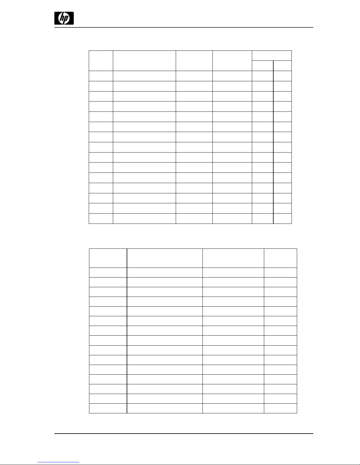
Recommended Spare Parts List-------------------------------------------------------------------------------------------------26
6) Block Diagram
Block diagram----------------------------------------------------------------------------------------------------------------------27
Page 5
Page 4
R15AAC/AAU (vs15)
1). Power Board Operation Therory
1.1Line filter consists of C801, T801, C802, C803, C804, C809, C815, C838, R801. It eliminates high frequency interference
to meet EMI’s requirement.
1.2Rec & Filter
Bridge diode D801 converts AC source into pulsed DC. This pulsed DC is smoothed and filtered by C805. R802 is
an NTC ( negative thermal coefficient ) resistor, used to reduce inrush current to be within safe range.
1.3Power transformer :
T802 converts energy for square wave from power source C805 to secondary side to generate +5V, +12V and
+21.5V.
1.4Output :
The square wave from T802 is rectified by D808 D809, D810, then filtered by C818, C824, C829, C813 ,C822 to
generate +21.5V and +12V, +5V respectively.
1.5Driver :
Q803 drive T802 from PWM control of I801 for power converted.
1.6FB :
Negative feedback CKT consists of photo coupler I802 and adjustable regulator I803. It can maintain output
voltages +21.5V and +12V, +5V at a stable level.
1.7PWM :
1.7.1Start : When power is turned on. C807 is charged a 12 volt and a starting current above 1mA to pin 1 of I801.
I801 starts to oscillate and outputs a pulse train through pin 6 to drive Q803.
1.7.2OPP : When Q803 turns on, C805 supplies a linearly increasing triangle current through the primary induc-
tance of T802 to the driver Q803, once the peak value of this current multiplied by R811 exceeds1 volt, pulse
train will be turn off immediately to protect Q803, T802 from being burned out.
1.7.3Regulation : If output voltage +21.5V goes up, the R terminal of I803 gets more bias, accordingly photo
transistor and photo diode flows more current. The voltage of pin 2 goes up too, making the pulse width of
pin 6 to become narrower. So the output voltage +21.5V will be pulled down to a stable value.
1.7.4OVP : If +21.5V goes up too much, the induced voltage on pin 4 of T802 becomes large also. Suppose that it
is over 18 volts. The pulse train at pin 6 goes down to zero, shutting Q803 off immediately.
1.7.5SCP : If output terminal is short to ground, photo transistor does not conduct, hence Q807 does not conduct
either. Then oscillation of I801 is stop, shutting Q803 off immediately.
Line
Filter
Rec. &
Filter
Power
Transformer
Outpur Rec. & Filter
PWM Driver
FB
Power Board Block Diagram
Page 6
Page 5
R15AAC/AAU (vs15)
2) Inverter Circuit
This unit operates on an output voltage of 21.5V from power source.
2.1VDD: R105 get a +5VDC for I101 power supply.
2.2Control IC: I101 (OZ9930)
2.2.1Enable : When pin 1 of I101 is over 0.55V, I101 works. If it is under 0.55V, I101 turns off.
2.2.2OSC: When I101 enabled, C104/C105 (pin 2 of I101) determine the operating frequency.
2.2.3SST: C106 (pin 1 of I101) provides soft start function.
2.2.4Ignition: IC provides higher operating frequency internally for more striking voltage until regulation of feedback of
lamp current. And provide 2 sec striking time.
2.2.5Dimming control: The divided voltage of R106/R103/R104 control the duty pulse of burst-mode to drive and
perform a wide dimming control for the CCFL. The burst-mode frequency is determined by operating freq/233.
2.2.6Regulation: Pin 8 of I101 provide regulation of the CCFL current from feedback. The non-inverting reference is at
1.25V nominal.
2.2.7Protection: Open-lamp protection in the ignition period is provided through pin 7 of I101.
Removal of the CCFL during normal operation will trigger IC to turns on and shuts off the inverter. This is latch
function.
2.2.8Output drivers: The configuration prevents any shoot-through issue associated with bridge-type power
conversion applications. Adjusting the overlap conduction between Q104, the CCFL current regulation is achieved.
2.3Half-bridge swit ching/Transformer: Q104, C122, C123 compose half-bridge swit ching to convert DC into AC for
driver the CCFL.
2.4Detection: C132, C112, C114, C126, R116, R115, C115 detect the output voltage and ensure a rated voltage by pin7
of I101 ensure not a open-lamp.
2.5Feedback: D116, D117, R111, R112, C109 sense the lamp current for negative feedback and regulation.
Inverter Board Block Diagram
VCC
VDD
Enable
OSC
SST
Output driver
Protection
Ignition
Regulation
Control IC : OZ9930
ON / OFF
Halfl-bridge switching
Transformer
Lamp
Feed back
Detection
VDD
Dimming Control
Brightness
Control
Page 7

Page 6
R15AAC/AAU (vs15)
3)Interface Operation
3.1Top (Circuit diagrams sheet 2 of 8)
This page is function block. (1) Power. (2) VGA & DDC interface. (3) Scaler GM2621.
(4) Key & panel interface. (5) Audio
3.2Power (Circuit diagrams sheet 3 of 7)
3.2.1P301 connector
A 5V power supply for flash ROM, EEPROM of EDID, logic. It is generated from the
P301 connector.
3.2.2I304 : 3-terminal regulator
A 3.3V power supply for I307 scaler IC gm2621 LCD module, it is generated from the 5V
source.
3.2.3I305 : 3-terminal regulator
A 1.8V power supply for I307 scaler IC gm2621, it is generated from the 3.3V source
(I304).
3.2.4Q302, I301 : ON/OFF control for LCD module power
ON/OFF control (PANELVCC_EN) is performed for power ON/OFF and also for the
power saving sequence. It is support 3.3V to LCD module power. The PANELVCC_EN
signal is generated from I307 scaler IC gm2621.
3.2.5R305: ON/OFF control for LCD module back light power
ON/OFF control (BKLT_EN) is performed for black light power ON/OFF and also for
the power saving sequence. The BKLT_EN signal is generation from I307 scaler IC
gm2621.
3.2.6Q301 : Adjust back light luminance for LCD module
It is adjusted back light luminance control (BKLT_ADJ) is performed for the back light
luminance. The BKLT_ADJ signal is generated from I307 scaler IC gm2621.
3.3VGA & DDC interface (Circuit diagrams sheet 4 of 7)
This sheet have RGB analog video signals input from VGA connector. Select H/V sync signals
source from VGA connector.
The RGB analog video signals input through AC-coupled, analog video signal is used to clamp the
black level at 0V. And H/V sync to sclaer.
And support DDC plug & play function for analog video.
3.3.1P302 connector
The RGB analog video input signals from the P302 connector.
3.3.2I306 DDC EEPROM
This IC is support DDC2B of the VESA standard, also plug and play for the PC host.
Page 8

Page 7
R15AAC/AAU (vs15)
3.4Scaler gm2621 (Circuit diagrams sheet 5 of 7)
The I307 gm2621 is all-in-one LCD monitor controller. The gm2621 leverages Genesis patented
advanced image-processing technology as well as a proven integrated ADC/PLL. Gm2621 also
integrates a micro-controller, an OSD controller, and dual LVDS.
The RGB analog video signal input entered from the video input circuit is converted into the digital
data of analog video signal through the incorporated A/D converter.
Based on this conversion, this device performs interpolation during pixel extension. These interpolation digital data are transformed to LVDS signal. The I307 source voltage is 3.3V and 1.8V, the
device clock source frequency is 14.318 MHz. And support keypad function.
3.4.1I310 SPI Flash ROM
The firmware program running from I310 external ROM, contains firmware code and data
for all firmware function, and control data and parameter and OSD related setting and other
service data. The device is 8bit configuration, 1024K bytes of ROM.
3.4.2I308 Microprocessor Supervisory Circuit
The function of this device is to assert a reset to I307 scaler gm2621, if either the power
supply dropped down.
3.4.3X301 14.318MHz
It generated reference clock input for I311 scaler.
3.4.4ISP and DDC2Bi function
The DDC2Bi is VESA standard for the host PC system, it can through DDC2Bi bus control
LCD monitor. Enter I307 pin54 DDC_SCL and pin55 DDC_SDA of the VGA port.
It use ISP function when change new firmware to I310 flash ROM. It used DDC2B port
IIC bus through I307 gm2621 to I310 flash ROM.
3.4.5The power save sequence function
First disable I307 pin49 (BKLT_EN) from H to L of LCD module back light power, delay
some time, then disable I307 pin127 (PANELVCC_EN) from H to L of LCD module
power, then I307 enter to power down mode.
Page 9
Page 8
R15AAC/AAU (vs15)
3.5Key & Panel interface (Circuit diagrams sheet 6of 7)
3.5.1P306 connector
It is LVDS bus, it is from I307 scaler to LCD panel module. The output voltage is 3.3V.
3.5.2P307 connector
The P307 has support keypad function. Control is give effect to for the push switch to be
used when the user changes the parameters, in order to modify the respective setting values.
Whether the switch has been pressed is identified with the switch input level that inputs a
DC voltage into I107 pin113 (LBADC_IN3) and pin114 (LBAD1_IN2).
Each switch input voltage based on Table 1.
Each parameter is stored in the I310 EEPROM, the contents of which are updated as
required.
The P307 have LED Blue and Amber light, the LED Blue signal from I307 pin 51, and the
LED Amber signal from I307 pin 56.
Table 1 Related ports of I311
Pin No. I/O Signal name Function Remarks Voltage
Pin 114 I KEY_POWER Soft power switch
input
Power key 1.05V
LBADC_
IN2
Pin 114 I KEY_MENU Enter OSD switch
input
Enter OSD menu 1.69V
Pin 113 I KEY_UP switch input Up key or
Source 2
2.3V
Pin 113 I KEY_DOWN
switch input Down key or
Source 1
1.9V
LBADC_
IN3
Pin 113 I KEY_SELECT Selection switch
input
Select key or
Auto adjust key
1.57V
↑
↓
Page 10

Page 9
R15AAC/AAU (vs15)
3.6Audio (Circuit diagrams sheet 7 of 7)
3.6.1P307 connector
The P307 is audio signal input from the keypad function board.
3.6.2P308 connector
The P308 have two audio function signals. One is audio volume control from the keypad
function board. Other is audio output to speaker or ear phone-jack.
3.6.3I312 TDA74965A
The I312 is 5x5W stereo audio amplifier, it is an integrated class-B dual output amplifier.
3.6.4Q308, I313: ON/OFF control for Audio power
ON/OFF control (AUDIO_PW) is performed for power ON/OFF and also for the audio
power down sequence. It is support 12V to audio power. The AUDIO_PW signal is
generated from I307 scaler IC gm2621.
3.6.5R385, Q309: MUTE control for Audio
MUTE control (MUTE) is performed for audio return to mute and also for the audio power
down sequence. The MUTE signal is generated from I307 scaler IC gm2621.
Page 11

Page 10
R15AAC/AAU (vs15)
3.7Others
3.7.1Detection of POWER switch status
The I307 gm2621 identifies the ON status of the two power supplies. The identification is
made when the power supply is turn off. For example, if the power supply is turn off with
the POWER switch, the POWER switch must be turn on when active the power supply
again. If the power supply is turned off by pulling out the power cord, then this power
supply can be turned on by connecting the power cord, without pressing the POWER
switch.
3.7.2Display mode identification
3.7.2.1Display mode identification
The display mode of input signal is identified based on Table 2.
When the mode has been identified through the measurement of horizontal and
vertical frequencies, the total number of lines is determined with a formula of “Hori-
zontal frequency / Vertical frequency = Total number of number of lines”. Final
identification can be made by examining the coincidence of the obtained figure with
the number of lines for the mode identified from the frequency. The Distinction
Hsync and Vsync of each mode is shown in Table 3.
When the detected frequency if the sync signal has changed, the total number of
lines should be counted even through it is range identified frequency in the same
mode.
3.7.2.2Out of range
This out of range mode is assumed when the frequency out of the horizontal /
vertical signal is as specified below.
Vertical frequency : 56 ~ 76 Hz.
Horizontal frequency : 30 ~ 63KHz.
3.7.2.3Power save mode
The power save mode is assumed when the horizontal / vertical signals are as
specified below.
If there is no horizontal sync signal input.
If there is no vertical sync signal input.
If the horizontal sync signal is outside the measuring range of I307 gm2621.
If the vertical sync signal is outside the measuring range of I307 gm2621.
●
●
●
●
●
●
●
●
●
Page 12
Page 11
R15AAC/AAU (vs15)
Polarity Mode
Resolution H-Freq
(KHz)
Band Width
(MHz)
H V
1 640x480 (59.94Hz) 31.469 25.175 - 2 640x480 (72Hz) 37.861 31.5 - 3 640x480 (75Hz) 37.5 31.5 - 4 720x400 (70Hz) 31.469 28.322 - +
5 800x600 (60Hz) 37.879 40 + +
6 800x600 (72Hz) 48.077 50 + +
7 800x600 (75Hz) 46.875 49.5 + +
8 832x624 (74.55Hz) 49.722 57.28 - 9 1024x768 (60Hz) 48.363 65 - -
10 1024x768 (75Hz) 60.023 78.75 + +
11 1152x870 (75Hz) 68.68 100 +/- +/12 1152x900 (76Hz) 71.71 105.6 - 13 1280x960 (60Hz) 60 108 +/- +/14 1280x1024 (60Hz) 63.981 108 + +
15 1280x1024 (75Hz) 79.976 135 + +
Table 2 video mode
Table 3 the Hsync, Vsync distinction
Indication
resolution
Distinction Hsync Distinction Vsync The fixed
mode
720 x 400
30.5KHz≦fH≦32.5KHz 69Hz≦fV≦71Hz
4
640 x 480
30.5KHz≦fH≦32.5KHz 59Hz≦fV≦61Hz
1
36.9KHz≦fH≦38.9KHz 71.8Hz≦fV≦73.8Hz
2
36.5KHz≦fH≦38.5KHz 74Hz≦fV≦76Hz
3
800 x 600
36.9KHz≦fH≦38.9KHz 59.3Hz≦fV≦61.3Hz
5
47.1KHz≦fH≦49.1KHz 71.2Hz≦fV≦73.2Hz
6
45.9KHz≦fH≦47.9KHz 74Hz≦fV≦76Hz
7
832 x 624
48.7KHz≦fH≦50.7KHz 73.5Hz≦fV≦75.5Hz
8
1024 x 768
47.4KHz≦fH≦49.4KHz 59Hz≦fV≦61Hz
9
59KHz≦fH≦61KHz 74Hz≦fV≦76Hz
10
1152 x 870
67.7KHz≦fH≦69.7KHz 74Hz≦fV≦76Hz
11
1152 x 900
70.7KHz≦fH≦72.7KHz 75Hz≦fV≦77Hz
12
1280 x 960
59KHz≦fH≦61KHz 59Hz≦fV≦61Hz
13
1280 x 1024
62.9KHz≦fH≦64.9KHz 59Hz≦fV≦61Hz
14
1280 x 1024
79KHz≦fH≦81KHz 74Hz≦fV≦76Hz
15
Page 13

Page 12
R15AAC/AAU (vs15)
3.7.3List of I/O Pin Assignments of the I311
Pin No.
Port Signal Name Initial
Setting
Function
51 GPIO0 LED_B L LED green enable
56 GPIO1 LED_A L LED amber enable
50 GPO4
BKLT_ADJ
- Backlight brightness control
57 GPO2 MUTE L Mute Audio
58 GPO3 AUDIO_PW L ON/OFF Audio power
115 LBADC_IN1 VGA_DETn H VGA cable connected
127 PPWR PANELVCC_EN L Panel power enable
49 PBIAS BKLT_EN L Back light power enable
Page 14
Page 13
R15AAC/AAU (vs15)
3)Trouble shooting
1.For Power Board
Check output voltage +5V, +12V, +21.5V are right or not
NG OK It is not power board problem
Check power switch is turn on or not
OK NG Turn switch on
Check power cord (P801), signal cable (P302), P802, P101, P102, P103,
P104 is connected right or not
OK
NG
Check C805 is about DC140V-330V or not
OK
NG
Check C807 is over 11V or not
OK
NG
Connect it right
Check F801, D801, P801 and repair them
Check pin 6 of I801 have same pulse or not
OK
NG
Check pin 1 of T802 have same pulse or not
OK
NG
Check peripheral component of I801 and repair them
Check L805, D804, I801 and repair them
Check peak voltage of R811 triangle pulse is up to 1 volt or not
OK
NG
Check D809, D810, D811, C818. C829, C813, C824, C822, T802 have
same short circuit or the output +5V, +12V, +21.5V is over load
OK
NG
Check feedback circuit around I802, I803 and the other components and
repair them
Repair them
Check D804, L805 and repair them
Check Q803, R813, R814, D806, R811, R815 and repair them
Page 15

Page 14
R15AAC/AAU (vs15)
2.For Inverter Circuit on Power Board
Check C102 pin is around 5V.
On/Off pin of P802 is over 2V.
Brightness pin is between 0V and 3.5V/
OK NG It is not inverter problem
Check pin6 of I101 is 5V
OK NG Check R105, C102 and repair them. Check printed wire.
Check P101, P102, D103 are connected right
OK
NG
Check pin 7 of I101 is over 3.1V
OK
NG
Check pin 2 of I101 is triangle pulse
OK
NG
Check CCFL and repair them. Lock P101, P102 tightly
Check Q106, Q107 and repair them
Check pin 1 of I101, there is soft start edge up to 4V and pin 4, 5. there
is some pulse outputs
OK
NG
Check pin 6 of I101, there is around 1.25V from output detection
OK
NG
Repair I101
Check C104, C105, I101 and repair them
Check SW MCS (Q104) work right
OK
NG
Check trabsfirner (T101) working it and repair it
Repair them
Check D116, D117, R111 and repair them
Page 16

Page 15
R15AAC/AAU (vs15)
3. No display of screen (Screen is black, color of LED is amber)
Does OSM display when you push
PROCEED buttom.
Yes
No Proceed "No OSM display" section.
Check if the sync signal from computer is
output and if the video cable is connected
normally. (VGA or DVI)
OK
Proceed "checking the resolution change IC
movement" section.
NG Input the sync signal of computer.
When a sugnal isn't being inputed, it is
indicated with "VIDEO INPUT". it is
indicated with "OUT OIF RANGE" at the
time of the frequency that it can't be
distinguished.
Page 17

Page 16
R15AAC/AAU (vs15)
4.Nothing displays on screen (Screen is black, color of LED is green)
Is backlight lit?
Refer "Checking the backlight unit" section"
OK
NG
Does computer output RGB video signals?
OK
Check OSM menu is display on screen
when you push the "PROCEED" key.
Proceed "Abnormal sreen" dection"
OK
NG
Check the video cable for failure. Check the host for output signal with
all black only.
1)Change pattern of video signal output on the host.
2)Rsconnect the video cable.
3)Change the video cable.
NG
Check if the LCD module signal cable is connected between the
Interface Board and LCD module.
OK
Next Page
NG
Failure Point
The LVDS cable is disconnected.
Page 18

Page 17
R15AAC/AAU (vs15)
Check the 5V power are supplied on P306
pin 1, 2, 3 (to the LCD panel)
Continue
OK
NG
Check if theVoltage on I304 pin2 that is
DC power at 3.3V.
OK
NG
Failure Point
1) I304 failure
Check if the TTL level on I301 pin1 that
TTL level is low (0~0.8V).
OK
NG
OK
NG
Failure Point
1) Prined wire broke between Q302
pin 3, R117, R308, C313 and I301
pin1.
2) Q312 is failure.
Failure Point
1) Printed wire broke between Q302 pin 2
and I307 pin127.
2) I307 is failure.
Check the PANELVCC_EN signal of the
rectangle input Q303 pin2 at TTL high
level.
Failure Point
I301 is failure.
Check the P306 all LVDS signals.
Failure Point
1) Printed wire broke between P306 and
I307 LVDS signals.
2) I307 is failure.
Failure Point
1) The LVDS cable broke between P306
and LCD module.
2) LCD module is failure.
OK
NG
Page 19

Page 18
R15AAC/AAU (vs15)
5.Checking the back light unit
Is +12V supplied to inverter PWB ? (by the
power board)
OK
NG
Failure Point
1) Inverter cable disconnection.
2) Power board failure.
Check the BKLT_EN signal of the
rectangle input P302 pin 6 at TTL high
level.
OK
NG
Failure Point
1) printed wire broke between P302 pin6,
R306 and I311pin 68.
2) R324, R325, C330 are open or short.
3) I311 is failure.
Check the BKLT_ADJ signal of the input
P302 pin5 from I311 pin98 is a PWM
signal.
OK
NG
Failure Point
1) printed wire broke between P302 pin5,
Q303, Q304 and I311 pin98.
2) Q303 or Q304 is failure.
2) I311 is failure.
Failure Point
Back light unit of LCD module is failure.
Page 20

Page 19
R15AAC/AAU (vs15)
6. Abnormal screen
6.1Abnormal screen for VGA source
Check the R, G, B video signal from computer
input on P302 of video connector.
OK
NG
Failure Point
1) No R, G, B video signals output from host
computer, check computer.
2) VGA video signal cable disconnection.
Check the R, G, B input video signals on I307
pin93, 96, 99 respectively that their level is 0.5
to 0.7Vp-p.
Failure Point
In the case of the Red signal. (Green and Blue
signal is the same path, too.)
1) Printed wire broke between P303 pin 1 and
I307 pin99.
2) Video cable is failure.
3) FB308, FB309, R313 are open.
4) R318 is short.
5) C325 is short or open.
6) C329 is short.
NG
OK
Check all LVDS signals being output to P306
from I307?
Failure Point
1) Printed wire broke between I311 and P305.
2) LVDS cable failure.
NG
OK
Prpcess "Checking the resolution change IC
movement" section.
Page 21

Page 20
R15AAC/AAU (vs15)
7.Abnormal OSM display adjust problem
Check the input DC voltage level whether was changed
when pressed function keys on the P307 pin 8, 9. (normal is
low level, when push buttom, generated a DC level plus)
(Refer table 1)
OK
NG
Failure Point
1) Function key wire disconnection.
2) Function key wire is failure.
3) Function key board is failure.
4) R390, R391 are open
5) R371, R370 are open or short
6) R365, R366, R367, R368, R369 are open or short or not correct
assistance.
Failure Point
I311 is failure.
Page 22

Page 21
R15AAC/AAU (vs15)
8. Abnormal plug and play operation
8.1 Abnormal plug and play operation for VGA
Confirm the host computersupplies DDC2 mode.
OK
NG
Failure Point
The host machine is not communicatiog in DDC2
mode.
Check the voltage on I306 pin8 that is power DC 5 V.
OK
NG
Failure Point
1) Printed wire broke between I306 pin8, D306, D309
and P302 pin9.
2) D306 is failure.
3) D310 is short.
Check the output signal of serial data / clock on I308
pin5, 6.
OK
NG
Failure Point
I308 is failure.
Check the voltage on P302 pin9 that is power
DC 5 V.
OK
NG
Failure Point
The VGA video cable is failure.
Check the voltage on P302 pin12, 15 that is serial data
/ clock signal.
OK
NG
Failure Point
The VGA video cable is failure.
Failure Point
1) Printed wire broke between I309 pin5, 6 and P302
pin12, 15.
2) R332, R333 is open.
3) C338, C339 is short.
Page 23

Page 22
R15AAC/AAU (vs15)
9.Checking the interface circuit of sync signal
9.1Checking the control circuit of horizontal sync pluse for VGA
9.2Checking the control circuit of vertical sync pluse for VGA
Check the horizontal sync signal on P302 pin13 TTL
level.
OK
NG
Failure Point
VGA Video cable is failure.
Check the horizontal sync signal on I307 pin189 TTL
level.
OK
NG
Failure Point
1) Printed wire broke between P302 pin13 and
I307 pin189.
2) R323 is open.
3) R326, C335 are short.
Failure Point
Process "Checking the resolution change IC
movement" section.
Check the horizontal sync signal on P302 pin14 TTL
level.
OK
NG
Failure Point
VGA Video cable is failure.
Check the horizontal sync signal on I307 pin90 TTL
level.
OK
NG
Failure Point
1) Printed wire broke between P302 pin13 and
I307 pin90.
2) FB315, R324 are open.
3) R325, C334 are short.
Failure Point
Process "Checking the resolution change IC
movement" section.
Page 24

Page 23
R15AAC/AAU (vs15)
10. Checking the resolution change IC movement
Check +3.3V supply on I307 pin2, 25, 47, 53, 91, 92, 74, 82, 101, 110,
116, 128.
OK
NG Proceed " Checking the DC/DC converter circuit" section.
Check +1.8V supply on I307 pin118, 87, 55, 17, 86, 78, 70, 104, 106.
OK
NG Proceed " Checking the DC/DC converter circuit" section.
Check X301 14.318MHz clock input to I307 pin108 and 109 at TTL
level.
OK
NG
Failure Point
1) Printed wire broke between X301 and I307 pin108, 109.
2) C347, C348 short or open.
3) X301 failure.
Check I307 pin111 RESETn signal is high level at normal operation.
OK
NG
Failure Point
1) Check I308 pin2 is low level wait 240ms to high level, when AC
power is plug in.
2) I308 failure.
3) Printed wire broke between I307 pin111 and I308.
2) C351 short.
3) I307 failure.
Check I307 pin59, 60, 61, 62,SPI_ROM control data
OK
NG
Failure Point
1) Printed wire broke between I307 pin59, 60, 61, 62 and I310.
2) I310 failure.
Failure Point
I307 failure.
Page 25

Page 24
R15AAC/AAU (vs15)
11. Audio no signal output
Check the audio signal input from the audio
source.
OK
NG
Failure Point
1) No audio signal from the audio source.
2) Audio cable is failure.
Check audio signal input of the I312
TDA7496SA pin5 .
Failure Point
1) FB322, FB323, R372, R373 are open. C385
C387, C391, C392 are short.
2) Audio output wire is disconnected from the
interface board P309 and key function board
P601.
3) Printed wire broke between P601 and J600 of
the function board.
NGOK
Check I312 pin13 have 12V power.
NG
OK
Check I3132 pin2 is 2V power
Next Page
NG
OK
Failure Point
1) FB303 is open.
2) +12V of power board output
failure
Check Q302 pin2 is TTL high level
NG
OK
Failure Point
1) R382 is open.
2) I307 failure
Check I313 pin1 is TTL low level
NG
OK
Failure Point
1) R560, R387, R381 are open.
Failure Point
1) I313 failure.
2) L301 is open.
Page 26

Page 25
R15AAC/AAU (vs15)
Check audio speaker is working.
OK
NG
Failure Point
1) Audio output wire is disconnected from the
interface board P309 to key function board
P601.
2) Printed wire broke between P601 and J600 for
the key function board.
3) C610, C609 are short.
4) J600 phone-jack is failure.
5) Audio speaker unit is disconnected from P602.
Failure Point
Audio speaker unit "L" or "R" is failure.
Check I312 pin10 Mute if is high level.
NG
OK
Failure Point
1) Printed wire broke between I307 pin57 and
Q309and I312 pin10.
2) R383, R384, R385, R338, C393 are open or
short.
3) Q312 is filure.
4) I307 is failure.
Continue
Check I316 pin4, 6 audio signal output.
NG
OK
Failure Point
1) Printed wire broke between I312 pin12, 14
and P309 pin1, 3.
2) C386, C388 open or short.
3) I312 is failure.
Page 27

Page 26
R15AAC/AAU (vs15)
5)Spare Parts
Recommended Parts List
Note: 1.The components identified by “ “ mark are critical for X-ray safety. Replace these with
only the same parts specified.
2.There is only OTP IC at the model beginning (FPR stage or before). When it put in mass
production and there must be Mask coming out. If you have spart parts need, please check
BOM to get the last release part number and related information.
No. Location Part Number Description
1 I301 6448018208 IC 24LC02B SOP-8 MICROCHIP
2 I306 6448018218 IC M24C02 SOP-8 ST
3 I301, I313 6444014708 FET P-Channel AO3401 SOT-23 AOS
4 I304 6442023326 IC Linear AIC1084-33CM TO-263
5 I305 6442040708 IC Linear AIC1117A-18CY SOT-223
6 I307 IC Scaler gm2621 PQFP-128P Genesis
7 I312 IC TDA7496SA
8 X301 6449006400 Crystal 14.318MHz AT-49 TOPICS
9 I310 IC flash ROM SST39SF020A-70 PLCC-32
SST
10 I801 6442097000 IC-LINEAR-FAN7601-8P-DIP-FAIRCH
ILD
11 I101 6442044700 IC-LINEAR-DZ9930D-8P0DIP-O2
12 T101, 102 6131022300 XFMER-TPW-1137-EEL19B
13 T801 6138004300 LINE FILTER 15Mh
14 T802 6131054010 XFRNER-TPW-1136-ER28
15 Q104,105 6444023100 IC-CMOS-AOP607
Page 28

5
5
4
4
3
3
2
2
1
1
D D
C C
B B
A A
Power &
Invertor
Board
H
H
P
P
D
D
-
-
V
V
S
S
1
1
5
5
/
/
V
V
S
S
1
1
7
7
/
/
V
V
S
S
1
1
9
9
B
B
l
l
o
o
c
c
k
k
D
D
i
i
a
a
g
g
r
r
a
a
m
m
P
P
3
3
0
0
1
1
L
L
V
V
D
D
S
S
Function
Key
Board
R,G,B,Hs,Vs
DSUB
P
P
3
3
0
0
6
6
Brightness, Inv_On/Off
F1705 -->P304
L
L
C
C
D
D
M
M
o
o
d
d
u
u
l
l
e
e
+
+
5
5
V
V
DDC
S
S
c
c
a
a
l
l
e
e
r
r
5V-3.3V
DC-DC
G
G
m
m
2
2
6
6
2
2
1
1
24LC02B
DDC_CLK,
DDC_DATA
3.3V-1.8V
A
A
n
n
a
a
l
l
o
o
g
g
V
V
i
i
d
d
e
e
o
o
I
I
n
n
p
p
u
u
t
t
P
P
3
3
0
0
2
2
Flash EPROM
SST25VF010
14.3MHz
X'TAL
ACpow er
input
(U niversal)
VS Series -->P307
I310
I307
I306
I304
I305
VS17 -> Panel 1. CPT CLAA170EA07
Panel 2. AUO M170EG01
VS19 -> Panel 1. LPL LM190E03
Panel 2. AUO M190EN04
VS15 -> Panel 1. AUO LM150XN07
Panel 2. CPT CLAA150XP01
PMC 25LVF010
I312
Audio AMP.
ST -7496S
A
P308
Audio In
P309
J600
To ear phone
P600
P601
P602
Speaker
Left
Right
+12V
+12V
Audio out
Audio input
Audio output Right/Left
CCFL
LVDS signal / Panel power
CCFL
HPD VS Series
Block Diagram
Custom11
Title:
Size:
CHECK:
Date:
Sheet: of
LITE-ON TECHNOLOGY CO.
DRAWN:
APPRO:
Date:
Date:
CHECK:
APPRO:
DESIGN: Date:
Date:
Date:
DWG.NO:
PCB. NO:
6) Block Diagram
R15AAC/AAU (vs15)
Page 27
Page 29

Page 30

Page 31

5
5
4
4
3
3
2
2
1
1
D D
C C
B B
A A
Nov 22 2004
POWER
R15AAX
4
SCHEMATIC REV 02 PTB-1579
1
0A Oct 05 '04
SHEET NO.
REVISION HISTORY
ROAD MAP
3
BY
BASED ON PTB-1551 Rev.0C SCHEMATICE FOR LITEON
DESCRIPTION
VGA & DDC INTERFACE
REV.
DESCRIPTION
TITLE SHEET
2
LAST UPDATE
5
KEY & PANEL INTERFACE
TOP
SCALER GM5621
6
Allen Lai
Allen Lai
Allen Lai
Allen Lai
7/30'04
7AUDIO
01 Revrsion change
Allen Lai
Nov. 13 '04
02 Add C405,C406,C407 for ESD protecter
Allen Lai
Nov. 22 '04
Allen Lai
8815790000-02
R15AAX
TITLE SHEET
Custom17
6832157900-02
Title:
Size:
CHECK:
Date:
Sheet: of
LITE-ON TECHNOLOGY CO.
DRAWN:
APPRO:
Date:
Date:
CHECK:
APPRO:
DESIGN: Date:
Date:
Date:
DWG.NO:
PCB. NO:
Page 32

5
5
4
4
3
3
2
2
1
1
D D
C C
B B
A A
Allen Lai Allen Lai
Allen Lai Allen Lai
8815790000-02
R15AAX
TOP
Custom27
6832157900-02
Title:
Size:
CHECK:
Date:
Sheet: of
LITE-ON TECHNOLOGY CO.
DRAWN:
APPRO:
Date:
Date:
CHECK:
APPRO:
DESIGN: Date:
Date:
Date:
DWG.NO:
PCB. NO:
4.SCALER GM5621_6
4.SCALER GM5621_6
PANELVCC_EN
BKLT_EN
R2N_CH3N_LV_E
R2P_CH3P_LV_E
G0N_CH2N_LV_E
G0P_CH2P_LV_E
G1N_CH1N_LV_E
G1P_CH1P_LV_E
G2N_CH0N_LV_E
G2P_CH0P_LV_E
CLKN_LV_E
CLKP_LV_E
R2N_CH3N_LV_O
R2P_CH3P_LV_O
CLKP_LV_O
CLKN_LV_O
G2P_CH0P_LV_O
G0P_CH2P_LV_O
G1N_CH1N_LV_O
G2N_CH0N_LV_O
G1P_CH1P_LV_O
G0N_CH2N_LV_O
RIN
GNDR
GIN
GNDG
BIN
GNDB
HS_IN
VS_I
N
DDC_SCL_VGA
DDC_SDA_VGA
VGA_DETn
LBADC_IN2
LBADC_IN3
LED_A
LED_G
BKLT_ADJ
DDC_WPn
3V3_SPI
T_ROE
T_RSP
T_ROWCLK
T_OSP
T_POL
T_LP
T_ESP
R0N_E
R0P_E
R1N_E
R1P_E
B0N_E
B0P_E
B1P_E
B1N_E
B2P_E
B2N_E
R0N_O
R0P_O
R1N_O
R1P_O
B0N_O
B0P_O
B1N_O
B1P_O
B2N_O
B2P_O
AUDIO_PW
MUTEn
VOLUME
2.POWER
2.POWER
BKLT_ADJ
BKLT_EN
PANELVCC_EN
5.KEY & PANEL INTERFACE
5.KEY & PANEL INTERFACE
LBADC_IN2
LBADC_IN3
LED_A
LED_G
R2N_CH3N_LV_E
R2P_CH3P_LV_E
G0N_CH2N_LV_E
G0P_CH2P_LV_E
G1N_CH1N_LV_E
G1P_CH1P_LV_E
G2N_CH0N_LV_E
G2P_CH0P_LV_E
R0N_E
R0P_E
R1N_E
R1P_E
CLKN_LV_E
CLKP_LV_E
B0N_E
B0P_E
B1N_E
B1P_E
B2N_E
B2P_E
R1N_O
R0N_O
R2P_CH3P_LV_O
R0P_O
R2N_CH3N_LV_O
R1P_O
T_ROE
T_RSP
T_ROWCLK
T_OSP
T_POL
T_LP
T_ESP
B0N_O
CLKP_LV_O
CLKN_LV_O
G1P_CH1P_LV_0
B1N_O
B2N_O
B1P_O
B0P_O
G0N_CH2N_LV_O
G1N_CH1N_LV_O
B2P_O
G0P_CH2P_LV_O
G2P_CH0P_LV_O
G2N_CH0N_LV_O
6.AUDIO
6.AUDIO
AUDIO_PW
MUTEn
VOLUME
3.VGA & DDC INTERFACE
3.VGA & DDC INTERFACE
VGA_DETn
DDC_SCL_VGA
DDC_SDA_VGA
DDC_WPn
HS_IN
VS_I
N
RIN
GNDR
GIN
GNDG
BIN
GNDB
3V3_SPI
LED_A
LED_A
BINB IN
LED_G
LED_G
DDC_SDA_VGA DDC_SDA_VGA
HS_IN HS_IN
VS_IN VS_IN
DDC_WPn DDC_WPn
PANELVCC_EN PANELVCC_EN
GNDR GNDR
LBADC_IN2
LBADC_IN2
DDC_SCL_VGA DDC_SCL_VGA
BKLT_ADJ BKLT_ADJ
BKLT_EN BKLT_EN
3V3_SPI3V3_SPI
GNDB GNDB
GNDG GNDG
GING IN
RINR IN
LBADC_IN3
LBADC_IN3
R2P_CH3P_LV_E R2P_CH3P_LV_E
R2N_CH3N_LV_E R2N_CH3N_LV_E
R1P_E R1P_E
R1N_E R1N_E
R0P_E R0P_E
R0N_E R0N_E
G2P_CH0P_LV_E G2P_CH0P_LV_E
G2N_CH0N_LV_E G2N_CH0N_LV_E
G1P_CH1P_LV_E G1P_CH1P_LV_E
G1N_CH1N_LV_E G1N_CH1N_LV_E
G0P_CH2P_LV_E G0P_CH2P_LV_E
G0N_CH2N_LV_E G0N_CH2N_LV_E
B2P_E B2P_E
B2N_E B2N_E
B1P_E B1P_E
B1N_E B1N_E
B0P_E B0P_E
B0N_E B0N_E
CLKP_LV_E CLKP_LV_E
CLKN_LV_E CLKN_LV_E
R2P_CH3P_LV_O R2P_CH3P_LV_O
R2N_CH3N_LV_OR2N_CH3N_LV_O
R1P_O R1P_O
R1N_O R1N_O
R0P_O R0P_O
R0N_OR0N_O
G2P_CH0P_LV_O G2P_CH0P_LV_O
G2N_CH0N_LV_O
G2N_CH0N_LV_O
G1P_CH1P_LV_O G1P_CH1P_LV_O
G1N_CH1N_LV_O G1N_CH1N_LV_O
G0P_CH2P_LV_O G0P_CH2P_LV_O
G0N_CH2N_LV_OG0N_CH2N_LV_O
B2P_O B2P_O
B2N_O B2N_O
B1P_O B1P_O
B1N_O B1N_O
B0P_O B0P_O
B0N_O B0N_O
CLKP_LV_O CLKP_LV_O
CLKN_LV_O CLKN_LV_O
T_ESP T_ESP
T_LP T_LP
T_POLT _POL
T_OSP T_OSP
T_ROWCLK T_ROWCLK
T_RSP T_RSP
T_ROE T_ROE
AUDIO_PW AUDIO_PW
MUTEn MUTEn
VGA_DETnVGA_DETn
VOLUME VOLUME
Page 33

5
5
4
4
3
3
2
2
1
1
D D
C C
B B
A A
D
SG
TO-252
E
CB
TO-263
Allen Lai
Allen Lai
Allen Lai
Allen Lai
8815790000-02
R15AAX
POWER
Custom37
6832157900-02
Title:
Size:
CHECK:
Date:
Sheet: of
LITE-ON TECHNOLOGY CO.
DRAWN:
APPRO:
Date:
Date:
CHECK:
APPRO:
DESIGN:
Date:
Date:
Date:
DWG.NO:
PCB. NO:
BACKLIGHT_ADJ
BKLT_ADJ
BACKLIGHT_EN
PANELVCC_EN
BKLT_EN
VCC5V
VCC5V
VLCD
VCC3V3 VCC1V8
VCC5V
VCC3V3
VCC5V
VCC3V3
VCC15V
R304
4K7
R389
100(NC)
R307
47K
C307
47uF/25V
C309
100uF/16V
P301
JWT-A2001WV2-08
1
2
3
4
5
6
7
8
R301
1K
C302
1uF
C308
0.1uF
C323
10uF/16V
C310
0.1uF
FB301 PBY160808T-121Y-S
C311
0.1uF
I301
AO3401
1
2 3
C304
0.01uF
FB304
PBY160808T-121Y-S(0)
I305
AIC1117A-18CY
1
23
4
ADJ
VOUTVIN
TAB
FB305
PBY160808T-121Y-S(NC)
C306
0.1uF
Q302
MMBT3904
2
1 3
C303
0.1uF
R308
4K7
FB302 PBY160808T-121Y-S
C322
22uF/16V
R305
100
Q301
MMBT3904
2
1 3
R309
4K7
R302
10K
C305
22uF/16V
FB306
PBY160808T-121Y-S
I304
AIC1084-33CM
1
23
4
ADJ
VOUTVIN
TAB
FB303 PBY160808T-121Y-S
C312
0.1uF
R306
10K
R303
16.9K
C313
1uF
C301
0.1uF(NC)
C324
22uF/16V
PANELVCC_EN5
BKLT_ADJ 5
BKLT_EN
5
Page 34

5
5
4
4
3
3
2
2
1
1
D D
C C
B B
A A
Allen Lai
Allen Lai
Allen Lai
Allen Lai
8815790000-02
R15AAX
VGA & DDC INTERFACE
Custom47
6832157900-02
Title:
Size:
CHECK:
Date:
Sheet: of
LITE-ON TECHNOLOGY CO.
DRAWN:
APPRO:
Date:
Date:
CHECK:
APPRO:
DESIGN: Date:
Date:
Date:
DWG.NO:
PCB. NO:
GIN
BIN
RIN
GNDB
GNDR
GNDG
VGA_SCL
DDC_SDA_VGA
DDC_WPn
DDC5V_A
VGA_5V
VGA_CONn
VGA_5V
VGA_SDA
VGA_BLUE
VGA_SCL
VGA_RED
VGA_GREEN
VGA_VSYNC
VGA_HSYNC
HS_IN
VS_IN
VGA_CONn
DDC_SCL_VGA
DDC_SDA_VGA
DDC_SCL_VGA
GREEN_IN
BLUE_IN
RED
GREEN
BLUE
RED_IN
VGA_DETn
VGA_SDA
DDC_5V 3V3_SPI
VCC5V
VCC5V VCC5V VCC5V
3V3_DVDD
C330
0.1uF
R326
2K2
C334
47pF
R331
4K7
D309
1N4148
P302
CONNECTOR DB15
8
15
7
14
6
13
5
12
4
11
3
10
2
9
1
16 17
I306
24C02
1
2
3
45
6
7
8
A0
A1
A2
GNDSDA
SCL
WP
VCC
FB314 BK2125HS431
C331
0.1uF
R316
75/1%
FB309 SBK160808T-600Y-S
D310
MMSZ5232B
D312
MMSZ5232B
C336
0.1uF
R333 100
R314 120
D306
MMSZ5232B
R324 100
R317
75/1%
D307 1N4148(NC)
C327 10nF
FB315 BK2125HS431
D305
MMSZ5232B
C338
47pF
D311
MMSZ5232B
R319 120
C332 10nF
C326 10nF
R320 100
R321 120
C335
47pF
R313 100
C328 10nF
R323 470
R330
4K7
D301
MMBD7000
3
1
2
C337
0.1uF
D304
MMSZ5232B
Q304
MMBT3904
2
1 3
C329
0.1uF
FB310 0
R318
75/1%
R325
2K2
R328
10K
FB312 0
D317
MMSZ5232B
C333 10nF
R327
0
R329
4K7
D308
1N4148
FB308 0
R315 100
FB311 SBK160808T-600Y-S
D303
MMBD7000
3
1
2
R322
100
D302
MMBD7000
3
1
2
C325 10nF
R332 100
C339
47pF
FB313 SBK160808T-600Y-S
RIN5
GNDR 5
GIN5
GNDG 5
BIN5
GNDB 5
VGA_DETn 5
HS_IN5
VS_IN5
DDC_SCL_VGA 5
DDC_SDA_VGA 5
DDC_WPn 5
3V3_SPI 5
Page 35

5
5
4
4
3
3
2
2
1
1
D D
C C
B B
A A
PIN51 High is disable, Low is enable, for the J-TAG port.
PIN119 High is UART on GPO, Low is UART on DDC.
7/30'04
PM25LV010
Allen Lai
Allen Lai Allen Lai
Allen Lai
8815790000-02
R15AAX
SCALER GM5621_6
C57
6832157900-
02
Title:
Size:
CHECK:
Date:
Sheet:
of
LITE-ON TECHNOLOGY CO.
DRAWN:
APPRO:
Date:
Date:
CHECK:
APPRO:
DESIGN: Date:
Date:
Date:
DWG.NO:
PCB. NO:
DDC_SCL_VGA DDC_SCL_VGA
DDC_SDA_VGA DDC_SDA_VGA
SPI_HOLDn
LED_G
VGA_DETn
SPI_DI
G1N_CH1N_LV_E
REX
T
LED_G
G1N_CH1N_LV_O
R2N_CH3N_LV_E
SPI_CLK
R2P_CH3P_LV_O
CLKN_LV_O
SPI_CLK
BKLT_ADJ BKLT_ADJ
CLKP_LV_E
G2P_CH0P_LV_O
TCLK
BKLT_EN
RESETn
G1P_CH1P_LV_O
GNDB GNDB
CLKN_LV_E
G0P_CH2P_LV_O
HS_IN HS_IN
XTAL
R2P_CH3P_LV_E
RIN RIN
UART_DO_SDA
G0N_CH2N_LV_E
SPI_CSn
VOLUME
G1P_CH1P_LV_E
G2N_CH0N_LV_E
R2N_CH3N_LV_O
BIN BIN
SPI_DI
PANELVCC_EN
LED_A LED_A
SPI_DO
G2P_CH0P_LV_E
G2N_CH0N_LV_O
GIN GIN
SPI_DO
UART_DI_SCL
G0P_CH2P_LV_E
VS_IN VS_IN
SPI_CSn
CLKP_LV_O
G0N_CH2N_LV_O
GNDG GNDG
GNDR GNDR
LBADC_IN1
LBADC_IN2
LBADC_IN3
LBADC_IN3
LBADC_IN2
VOLUME
3V3_SPI
3V3_SPI
T_ROE
T_RSP
T_ROWCLK
T_OSP
T_POL
T_LP
T_ESP
R0N_E
R0P_E
R1N_E
R1P_E
B0N_E
B0P_E
B1N_E
B1P_E
B2N_E
B2P_E
R0N_O
R0P_O
R1N_O
R1P_O
B0N_O
B0P_O
B1N_O
B1P_O
B2N_O
B2P_O
AUDIO_PW
MUTEn
LED_A
LED_G
DDC_WPn
SPI_WP
RESETn
SPI_WP
3V3_AVDDVCC3V3
3V3_LVVCC3V3
VCC1V8
VCC1V8 1V8_CVDD
3V3_DVDD
VCC3V3
3V3_RPLL
VCC3V3 3V3_RPLL
3V3_LV
VCC5V
3V3_AVDD
3V3_RPLL
3V3_AVDD 1V8_AVDD
1V8_AVDD
3V3_DVDD
3V3_DVDD
1V8_CVDD3V3_DVDD
VCC5V
C366
0.1uF
C345
0.1uF
C367
0.1uF
R388 4k7
R337 0
C376
0.1uF
C346
0.1uF
C375
0.1uF
C359
0.1uF
C343
0.1uF
I307
gm5621
PQFP-128
99
100
96
97
93
94
73
72
76
75
81
80
108
109
123
124
125
126
38
37
84
83
69
59
60
64
65
66
67
111
121
122
127
49
89
90
5488117
63
30
29
18
28
36
35
24
21
23
22
20
19
27
6
5
4
3
39
40
42
33
34
31
32
15
16
41
11
12
9
10
7
8
14
13
51
56
57
58
50
119
120
115
114
113
112
110
101928274128225475391116
118875517867870
104
106
43
44
45
46
105
687177799598102
1072648
185103
52
61
62
RED+
REDGREEN+
GREENBLUE+
BLUE-
RX2-
RX2+
RX1-
RX1+
RX0-
RX0+
XTAL
TCLK
OSP/GPIO_11
POL/GPIO_12
LP/GPIO_13
ESP/GPIO_14
O_G1P/CH1P_LV_O
O_G1N/CH1N_LV_O
RXC-
RXC+
REXT
SPI_CSn
SPI_CLK
DDC_SCL_VGA
DDC_SDA_VGA
DDC_SCL_DVI
DDC_SDA_DVI
RESETn
RSP/GPIO_9
ROWCLK/GPIO_10
PPWR
PBIAS
HSYNC
VSYNC
CRVSS
CRVSS
CRVSS
RESERVED
O_R1P/RESERVED
O_R1N/RESERVED
CRVSS
O_R0P/RESERVED
O_G0P/CH2P_LV_O
O_G0NCH2N_LV_O
E_B2P/RESERVED
E_B1N/RESERVED
E_B2N/RESERVED
E_B1P/RESERVED
E_B0P/RESERVED
E_B0N/RESERVED
O_R0N/RESERVED
E_R1P/RESERVED
E_R1N/RESERVED
E_R0P/RESERVED
E_R0N/RESERVED
O_G2N/CH0N_LV_O
O_G2P/CH0P_LV_O
O_B0P/RESERVED
OCLKN/CLKN_LV_O
OCLKP/CLKP_LV_O
O_R2N/CH3N_LV_O
O_R2P/CH3P_LV_O
E_G2N/CH0N_LV_E
E_G2P/CH0P_LV_E
O_B0N/RESERVED
E_G0N/CH2N_LV_E
E_G0P/CH2P_LV_E
ECLKN/CLKN_LV_E
ECLKP/CLKP_LV_E
E_R2N/CH3N_LV_E
E_R2P/CH3P_LV_E
E_G1P/CH1P_LV_E
E_G1N/CH1N_LV_E
GPO_0
GPO_1
GPO_2
GPO_3
PWM0/GPO_4
PWM1/GPO_5
ROE/GPIO_8
LBADC_IN1
LBADC_IN2
LBADC_IN3
LBADC_RETURN
AVDD_RPLL_33
AVDD_ADC_33
AVDD_ADC_33
AVDD_DVI_33
AVDD_DVI_33
AVDD_BIAS_33
VDD_OUT_33
VDD_OUT_33
VDD_OUT_33
RVDD_33
RVDD_33
LBADC_VDD_33
CVDD_18
CVDD_18
CVDD_18
CVDD_18
AVDD_DVI_18
AVDD_DVI_18
AVDD_DVI_18
AVDD_ADC_18
VDD_RPLL_18
O_B1N/RESERVED
O_B1P/RESERVED
O_B2N/RESERVED
O_B2P/RESERVED
VBUFC_RPLL
AVSS_DVI
AVSS_DVI
AVSS_DVI
AVSS_DVI
AVSS_ADC
AVSS_ADC
AVSS_ADC
AVSS_RPLL
VSS_OUT
VSS_OUT
AVSS_BIAS
AVSS_DVI
AVSS_ADC
CRVSS
SPI_DI
SPI_DO
C348 2.2pF
FB316
PBY160808T-121Y-S
R334
250/1%(NC)
X301
14.318MHZ
C407
0.1uF
FB320
PBY160808T-121Y-S
C363
0.1uF
R339
10K
R344
820K
C347 15pF
R343
820K
C358
0.1uF
C354
0.1uF
C342
10uF/16V
C352
0.1uF
I309
NC74AHCT1G08DCK/NC7ST08P5
1
2
3
4
5
A
B
GND
Y
VCC
R340
10K
FB321
PBY160808T-121Y-S
C364
0.1uF
C374
0.1uF
C362
0.1uF
C344
0.1uF
C351
10nF
C361
0.1uF
FB319
PBY160808T-121Y-S
C365
10uF/16V
C357
0.1uF
C340
1uF
R338 0
C341
0.1uF
C349
1uF
I310
SST25VF010
1
2
3
4 5
6
7
8
CE#
SO
WP#
GND SI
SCK
HOLD#
VCC
C353
10uF/16V
C372
0.1uF
C369
0.1uF
R346 0
C371
0.1uF
Q310
MMBT3906
FB318
PBY160808T-121Y-S
R336
2k2
C368
0.1uF
R345
10K
I308
MIC809MU
1
2
3
GND
RST
VCC
C360
10uF/16V
C356
0.1uF
C350
0.1uF
C370
0.1uF
FB317
PBY160808T-121Y-S
R335
10K(NC)
R347
100K
C355
0.1uF
PANELVCC_EN 3
BKLT_EN 3
R2N_CH3N_LV_E 6
R2P_CH3P_LV_E 6
G0N_CH2N_LV_E 6
G0P_CH2P_LV_E 6
G1N_CH1N_LV_E 6
G1P_CH1P_LV_E 6
G2N_CH0N_LV_E 6
G2P_CH0P_LV_E 6
CLKN_LV_E
6
CLKP_LV_E 6
R2N_CH3N_LV_O 6
R2P_CH3P_LV_O 6
CLKP_LV_O 6
CLKN_LV_O 6
G2P_CH0P_LV_O 6
G0P_CH2P_LV_O 6
G1N_CH1N_LV_O 6
G2N_CH0N_LV_O 6
G1P_CH1P_LV_O 6
G0N_CH2N_LV_O 6
RIN4
GNDR4
GIN4
GNDG4
BIN4
GNDB4
HS_IN4
VS_IN4
DDC_SCL_VGA4
DDC_SDA_VGA4
VGA_DETn4
LBADC_IN26
LBADC_IN36
LED_A6
LED_G6
BKLT_ADJ3
VOLUME7
3V3_SPI4
3V3_SPI4
T_ROE 6
T_RSP 6
T_ROWCLK6
T_OSP6
T_POL 6
T_LP6
T_ESP 6
R0N_E 6
R0P_E 6
R1N_E 6
R1P_E 6
B0N_E 6
B0P_E 6
B1P_E 6
B1N_E 6
B2P_E 6
B2N_E 6
R0N_O 6
R0P_O 6
R1N_O 6
R1P_O 6
B0N_O 6
B0P_O 6
B1N_O 6
B1P_O 6
B2N_O 6
B2P_O 6
AUDIO_PW7
MUTEn7
DDC_WPn4
Page 36

5
5
4
4
3
3
2
2
1
1
D D
C C
B B
A A
Note: Pin19 is no pin header
FOR LVDS INTERFACE
LBADC_IN2
LBADC_IN3
KEY_POWERn
KEY_MENUn KEY_DOWNn KEY_UPn KEY_SELECTn
1.57V2.3V1.9V
1.05V 1.69V
If it is 15" panel used 2x10 pin connector.
If it is 17" panel used 2x16 pin connector.
PIN#
1
2
3
4,5
7
8,9
16
CPT
NC
GND
NC
NC
3V3
3V3
?
HANNSTAR
NC
NC
NC
NC
3V3
3V3
?
MINUS+PLUS -- > 2.6V On LBADC_IN3
POWER+MENU -->2.01V On LBADC_IN2
(*464)
Allen Lai Allen Lai
Allen LaiAllen Lai
8815790000-02
R15AAX
KEY & PANEL INTERFACE
Custom67
6832157900-02
Title:
Size:
CHECK:
Date:
Sheet: of
LITE-ON TECHNOLOGY CO.
DRAWN:
APPRO:
Date:
Date:
CHECK:
APPRO:
DESIGN: Date:
Date:
Date:
DWG.NO:
PCB. NO:
LED_G
LED_A
LED_AMBER
LBADC_IN3
LED_BLUE
B_LED
A_LED
LBADC_IN2
R2P_CH3P_LV_E
CLKN_LV_E
G1N_CH1N_LV_E
G2N_CH0N_LV_O
G0P_CH2P_LV_O
CLKP_LV_E
CLKN_LV_O
R2N_CH3N_LV_O
G2P_CH0P_LV_O
G1P_CH1P_LV_E
R2N_CH3N_LV_E
G1P_CH1P_LV_O
CLKP_LV_O
G1N_CH1N_LV_O
R2P_CH3P_LV_O
G0N_CH2N_LV_O
T_ROWCLK
T_RSP
T_LP
T_ROE
T_POL
T_OSP
T_ESP
CLKP_LV_E
R1P_E
G2N_CH0N_LV_E
R1N_E
G0N_CH2N_LV_E
B1P_E
R2N_CH3N_LV_E
R0P_E
CLKN_LV_E
B1N_E
B2P_E
G2P_CH0P_LV_E
R0N_E
B0P_E
B2N_E
G0P_CH2P_LV_E
R2P_CH3P_LV_E
B0N_E
R1N_O
R2P_CH3P_LV_O
R0P_O
R2N_CH3N_LV_O
R0N_O
R1P_O
B1N_O
G0P_CH2P_LV_O
B0P_O
G1P_CH1P_LV_O
G0N_CH2N_LV_O
G1N_CH1N_LV_O
B2P_O
B1P_O
B2N_O
B0N_O
CLKN_LV_O
CLKP_LV_O
G2N_CH0N_LV_O
G2P_CH0P_LV_O
G1N_CH1N_LV_E
G1P_CH1P_LV_E
G0N_CH2N_LV_E
G0P_CH2P_LV_E
G2N_CH0N_LV_E
G2P_CH0P_LV_E
KEY_POWERn
KEY_MENUn
KEY_DOWNn
KEY_UPn
KEY_SELECTn
B_LED
A_LED
LBADC_IN3
LBADC_IN2
KEY_POWERn
KEY_MENUn
KEY_DOWNn
KEY_UPn
KEY_SELECTn
VCC5V
VLCD
VCC3V3
VLCD
VLCD
VCC3V3
VCC5V
C384
0.1uF
R370
4K7
P305
AF730X-AXG1T(P-TWO)
1
2
3
4
5
6
7
8
9
10
11
12
13
14
15
16
17
18
19
20
21
22
23
24
25
26
27
28
29
30
31
32
C406
0.1uF
R371
4K7
R359
2K2
R358 0(NC)
P304
AF750X-AXG1T(P-TWO)
1
2
3
4
5
6
7
8
9
10
11
12
13
14
15
16
17
18
19
20
21
22
23
24
25
26
27
28
29
30
31
32
33
34
35
36
37
38
39
40
41
42
43
44
45
46
47
48
49
50
51
52
Q306
MMBT3904
2
1 3
C378
0.1uF(NC)
R362
2K2
P306
JWT-A2003WV2-2x16P-T3
1
2
3
4
5
6
7
8
9
10
11
12
13
14
15
16
17
18
19
20
21
22
23
24
25
26
27
28
29
30
31
32
R392
10K
Q311
MMBT3906
3
2
1
Q305
MMBT3904
2
1 3
R363 470
C379
0.1uF(NC)
R364 200
C380 0.1uF
R365 10K
R350 10K(NC)
R393 10K
R351 0(NC)
R367 4K7
C382 0.1uF
R348 10K(NC)
C383
0.1uF
R368 2K
R366 3K3
C381 0.1uF
R390 220
R356 0(NC)
R361
10K(NC)
R360
10K(NC)
P307
JWT-A2001WV2-10
1
2
3
4
5
6
7
8
9
10
R391 220
C403 0.1uF
C405
0.1uF
R369 5K6
R349
0(NC)
R357 0(NC) C404 0.1uF
R352 0(NC)
TP1
POINT
LBADC_IN25
LBADC_IN35
LED_A5
LED_G5
R2N_CH3N_LV_E5
R2P_CH3P_LV_E5
G0N_CH2N_LV_E5
G0P_CH2P_LV_E5
G1N_CH1N_LV_E5
G1P_CH1P_LV_E5
G2N_CH0N_LV_E5
G2P_CH0P_LV_E5
R0N_E5
R0P_E5
R1N_E5
R1P_E5
CLKN_LV_E5
CLKP_LV_E5
B0N_E5
B0P_E5
B1N_E5
B1P_E5
B2N_E5
B2P_E5
R1N_O5
R0N_O5
R2P_CH3P_LV_O5
R0P_O5
R2N_CH3N_LV_O5
R1P_O5
T_ROE5
T_RSP5
T_ROWCLK5
T_OSP5
T_POL5
T_LP5
T_ESP5
B0N_O5
CLKP_LV_O5
CLKN_LV_O5
G1P_CH1P_LV_05
B1N_O5
B2N_O5
B1P_O5
B0P_O5
G0N_CH2N_LV_O5
G1N_CH1N_LV_O5
B2P_O5
G0P_CH2P_LV_O5
G2P_CH0P_LV_O5
G2N_CH0N_LV_O5
CLKP_LV_O5
R2P_CH3P_LV_O5
G1N_CH1N_LV_O5
G0P_CH2P_LV_O5
G2P_CH0P_LV_O5
G2N_CH0N_LV_O5
G1P_CH1P_LV_05
R2N_CH3N_LV_O5
G0N_CH2N_LV_O5
CLKN_LV_O5
G0N_CH2N_LV_E5
G2P_CH0P_LV_E5
G2N_CH0N_LV_E5
G0P_CH2P_LV_E5
CLKN_LV_E5
G1N_CH1N_LV_E5
G1P_CH1P_LV_E5
R2P_CH3P_LV_E5
R2N_CH3N_LV_E5
CLKP_LV_E5
LBADC_IN25
LBADC_IN35
Page 37

5
5
4
4
3
3
2
2
1
1
D D
C C
B B
A A
GS
D
AUDIO_PW
MUTEn
Audio Function
XXX
LOW HIGH
LOW
HIGH
HIGH
OFF MUTEON
C399 modify to 0.1uF
4K7
10K
Allen Lai
Allen Lai
Allen Lai
Allen Lai
8815790000-02
R15AAX
AUDIO
Custom77
6832157900-02
Title:
Size:
CHECK:
Date:
Sheet:
of
LITE-ON TECHNOLOGY CO.
DRAWN:
APPRO:
Date:
Date:
CHECK:
APPRO:
DESIGN: Date:
Date:
Date:
DWG.NO:
PCB. NO:
OUT_R
AMP_15V
MUTEn
MUTEn
AUDIO_PW
AUDIO_IN_R
AUDIO_IN_L
AMP_MUTE
AMP_IN_R
AMP_IN_L
AMP_15V
AMP_MUT
E
OUT_L
AUDIO15V
VOLUME
AMP_VOLUME
VCC15V
S-GND
S-GND
S-GND
S-GND
L301
45uH DRWW 10 X 10
C401
100uF/25V
C397
0.1uF
C388 470uF/25V
D315
MMSZ5232B(NC)
C392
47pF
R373 1K
C396
470uF/25V
Q308
MMBT3904
2
1 3
R377 20k
C402
0.1uF(NC)
D313
MMSZ5232
B(NC)
C391
47pF
FB325
PBY201209T-301Y-S
I313
AO3401
1
2 3
P309
JWT-A2001WV2-03
1
2
3
C387 0.22uF
R381
3k3
FB323 PBY160808T-121Y-S
I312
TDA7496SA
6
1
5
7
3
4
12
10
9
14
8
11
13
15
2
NC
INR
INL
SVR
VOL
VAO_L
OUTL
MUTE
STBY
OUTR
S_GND
PW_GND
VS
PW_GND
VAO_R
Q309
MMBT3904
2
1 3
R383
10K
C386 470uF/25V
R385
4K7
R382
4K7
R372 1K
D314
MMSZ5232
B(NC)
FB324
PBY160808T-121Y-S
P308
PH-JACK-3P
3
2
1
C400
0.1uF
D316
MMSZ5232B(NC)
R387
1k
R378
22k
C395
0.1uF
C399
0.1uF
R374
47K
R375
47K
R386
150K
FB322 PBY160808T-121Y-S
R380
1k
R384
6k8
C398
0.1uF
C394
470uF/25V
C385 0.22uF
C393
1uF
AUDIO_PW5
MUTEn5
VOLUME5
Page 38

5
5
4
4
3
3
2
2
1
1
D D
C C
B B
A A
NS TSAI
NS TSAI
STEPHEN SC LIN
ROGER CHANG
10-7-2004
10-7-2004
10-7-2004
10-7-2004
21.5V
GND
12V
BRI
ON-OFF
11
TITLE SHEET
HP-R15AAC
8815630000-01
6832156300-01
Title:
Size:
CHECK:
Date:
Sheet: of
LITE-ON TECHNOLOGY CO.
DRAWN:
APPRO:
Date:
Date:
CHECK:
APPRO:
DESIGN:
Date:
Date:
Date:
DWG.NO:
PCB. NO:
+5V
GND
GNDGND
GND
GND
GND
GND
GND
GND
GND
GND
GND
GND
GND
GND
GND
GND-1
GND
GND
GND
GND-1
GND-1
GND
GND
GND-1
GND
GND GND
GND
GND-1
GND
GND
GND-1
GND-1
GND-1
GND-1
1
2
2P
P102
1
2
R104
475K
VR801
10K
R836
1M
AOP605
Q104
3
8
6
5
2
1
7
4
S1D2D1
D1
G2S2D2
G1
+
C829
1000uF/25V
12
D117
1N4148
2 1
Q841
A733
3
1
2
+
C123
470uF/25V
12
R119
1M
R116
3M 1/4W
C827
0.01uF/PEM
C806
0.01uF/1KV
I803
AP431
1 2
3
D111
1N4148
21
C104
330P
D114
1N4148
21
C109
0.068uF
PEM
R841
5.1K
R133 10
C803
2200P/250V-Y
L803
BEAD/6mm
R134
2K
T801
ET-20
1 2
43
R827
26.1k
MF
1%
+
C842
10uF/50V
12
R117
100K
Q803
8N60C
3 2
1
C108
1000P
R802
SCK083
D806
1N4148
21
1
2
3
6
5
4
P802
20-6P1
1
2
3
4
5
6
R105
22
D810
SB360
2 1
+
C807
47uF/25V
12
D116
1N4148
21
+
C120
1uF/50V
12
L805
56UH
R835
1M
I805
AP431
1 2
3
T101
EEL19-B
1
2
3
4
5
6107
Q107
C945
2
1 3
Q805
FQP13N06L
3
2
1
C106
0.047uF
+
C805
68uF/400V
12
D808 SF34G
2 1
C112
22P/3KV
D103
1N4148
21
C114
10P/3KV
C833
0.1UF
R828
1K
+
C813
1000uF/25V
12
F801
3.15A/250V
D841
1N4148
21
D803
PG108R
2 1
R842
4.7K
R102
100K
+
C808
0.47uF/50V
12
D801
KBP205G
3
4
2
1
+
C103
2.2uF/50V
12
C841
220P
C809
1000P/1KVX7R
C816
*(N.M.)
D804
UF4005G
21
R811
0.68 2W
R801
1M MGF
+
C818
470uF/35V
12
C811
220P
C831
4700PF
PEM
+
C124
220uF/35V
12
R824
33K
MF
1%
C821
1000P/100VX7R
R813
100
MOF
C105
27P
R830
5.6K
C132
22P/3KV
D809 SF34G
2 1
C801
0.33uF/250V-X
R823
270
C834
1000P/PEM
R118
100K
+
C824
1000uF/10V-KF
12
R132
2K
+
C102
22uF/50V
12
Q806
C945
2
1 3
1
2
2P
P101
1
2
R106
649K
R815
470
MOF
C815
0.01uF
1KV
C838
0.1uF/250V-X
D106
1N4148
21
C832
1000P/500VX7R
R825
1K
R113
1M
OZ9RRBDI101
3
8
6
5
2
1
7
4
GND
ISEN
VDD
DRV1
CT
ENA_SST
VSEN_DIM
DRV2
R826
1K
D811
24B
C110
0.01uF
PEM
R814
20K
MOF
R111
340 1%
8
4
167
2
53
I801
FAN7601
I802
LTV817
1
2
4
3
C810
100P/1KVX7R
R834
JUMP
R832
8.2K 1%
D802
P6KE150A
+
C822
1000uF/10V-KF
12
C115
5100P
PEM
Q106
C945
2
1 3
C802
3300P/250V-Y
R804
360K
1/4W
MGF
R817
1K
D115
1N4148
2 1
D101
1N4148
21
R808
39K 1%
+
C122
470uF/25V
12
T802
ER-28F
3
1
456
7
8
9
10
Q108
2N7000
1 3
2
Q102
C945
3
1
2
R112
1K
R115
4.64K 1%
C126
10P/3KV
C804
2200P/250V-Y
R103
200K
C812
0.1UF
R829
100
F802
JUMP WIRE
R831
31.6K 1%
R818
910/2W
N
L
FG
ACSOCKET
P801
1
3
2
ZD801
*.*
R131 10
Q103
A733
3
1
2
Q101
2N7000
2
31
R101
100K
+
C828
4.7uF/50V
12
Page 39

Page 40

Page 41

Page 42

Page 43

Page 44

Page 45

Page 46

LITE-ON TECHNOLOGY CORP.
16 F, 392, Rueykuang. Road, Taipei, Taiwan
Tel: 886-2-87982888Fax: 886-2-87982829Printed in Taiwan
 Loading...