

Hp PROLIANT ML150 G2, PROLIANT ML310 G4, PROLIANT ML330 G2, PROLIANT ML350 G2, PROLIANT DL145 Fully-Buffered DIMM technology
...Page 1

Fully-Buffered DIMM technology in HP ProLiant servers
technology brief
Abstract.............................................................................................................................................. 2
Introduction......................................................................................................................................... 2
Performance barriers for traditional DIMM.............................................................................................. 2
Fully-Buffered DIMM architecture ........................................................................................................... 4
Benefits........................................................................................................................................... 6
Simplified board design ................................................................................................................ 6
Higher memory capacity ............................................................................................................... 6
Higher performance...................................................................................................................... 7
Improved reliability....................................................................................................................... 7
Challenges...................................................................................................................................... 8
Latency ....................................................................................................................................... 8
Power and thermal loads............................................................................................................... 8
Performance tuning, achieving maximum performance ............................................................................. 9
Conclusion.......................................................................................................................................... 9
For more information.......................................................................................................................... 10
Call to action .................................................................................................................................... 10
Page 2
Abstract
This paper describes the features, benefits, and challenges of Fully-Buffered dual inline memory
module (FB-DIMM) technology. It also provides rules for populating FB-DIMM slots to achieve
maximum performance in HP ProLiant servers.
Introduction
HP ProLiant servers provide balanced system architectures that deliver peak performance per watt of
power. A balanced system architecture is one in which the three main server subsystems—processing,
memory, and I/O—interact efficiently to maximize CPU performance. The introduction of dual-core
processor technology challenged HP engineers to improve the performance of the memory and I/O
subsystems to maintain system balance. Engineers overcame the performance bottleneck of the
parallel I/O bus by migrating to a high-speed serial interface with technologies such as SerialAttached SCSI, Serial ATA, and PCI Express. Likewise, some memory subsystems are migrating to
high-speed serial FB-DIMM technology to deliver scalable bandwidth and memory capacity that is not
possible with traditional DIMM technologies.
The paper describes the barriers that limit memory capacity and performance of servers that use
traditional DIMM technologies. This paper also describes the operation of FB-DIMMs and summarizes
the benefits and challenges of using FB-DIMM technology.
Performance barriers for traditional DIMM
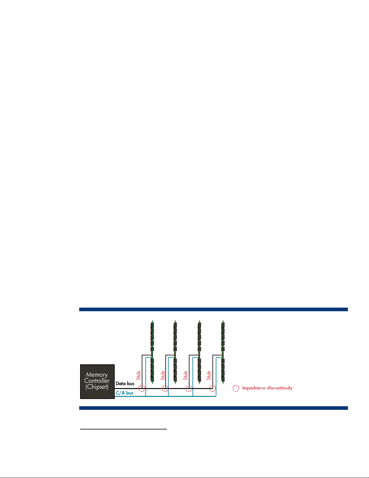
Traditional DIMM architectures use a stub-bus topology with parallel branches (stubs) that connect to
a shared memory bus (Figure 1). The memory bus consists of the command/address (C/A) bus and
the data bus. The C/A bus consists of 21 data traces that transport command and address signals to
the DIMMs. The data bus consists of 72 traces, each carrying one bit at a time (a total of 64 data bits
and 8 ECC
electrical signals from the memory controller to reach the DIMM bus-pin connections at the same time,
all the traces have to be the same length. This often results in circuitous traces on the motherboard
between the memory controller and memory slots. Both the latency (delay) resulting from complex
routing of traces and signal degradation at the bus-pin connections cause the error rate to increase as
the bus speed increases.
Figure 1. Stub-bus topology. An impedance discontinuity is created at each stub-bus connection.
1
bits). Each DIMM connects to the data bus using a set of pin connectors2. In order for the
1
Error correcting code
2
Typical SDRAM DIMMs have a total of 168 pins, DDR DIMMs have 184 pins, and DDR2 DIMMs have 240 pins.
2
Page 3
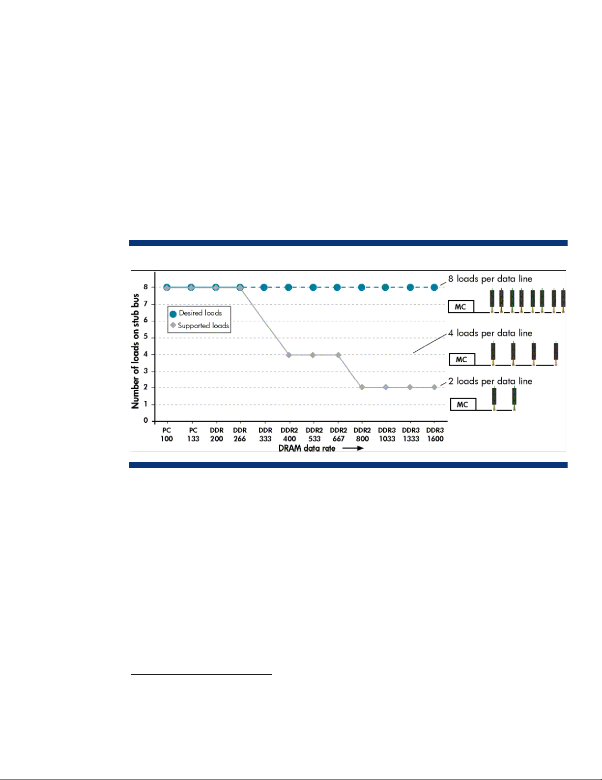
Each stub-bus connection creates an impedance discontinuity that negatively affects signal integrity. In
addition, each DIMM creates an electrical load on the bus. The electrical load accumulates as DIMMs
are added. These factors decrease the number DIMMs per channel that can be supported as the bus
speed increases. For example, Figure 2 shows the number of loads supported per channel at data
rates ranging from PC 100 to DDR-3 1600. Note that the number of supported loads drops from eight
to two as data rates increase to DDR2 800.
Increasing the number of channels to compensate for the drop in capacity per channel was not a
viable option due to increased cost and board complexity. System designers had two options: limit
memory capacity so that fewer errors occur at higher speeds, or use slower bus speeds and increase
the DRAM density. For future generations of high-performance servers, neither option was acceptable.
Future generations of servers require an improved memory architecture to achieve higher memory
bandwidth and capacity. Consequently, JEDEC
3
developed the Fully-Buffered DIMM specification, a
serial interface that eliminates the parallel stub-bus topology and allows higher memory bandwidth
while maintaining or increasing memory capacity.
Figure 2. Maximum number of loads per channel based on DRAM data rate.
3
The Joint Electron Device Engineering Council (JEDEC) is the semiconductor engineering standardization body
of the Electronic Industries Alliance. HP works with JEDEC memory vendors and chipset developers during
memory technology development to ensure that new memory products fulfill customer needs in regards to
reliability, cost, and backward compatibility.
3
Page 4

Fully-Buffered DIMM architecture
The FB-DIMM architecture has serial links between the memory controller and the FB-DIMMs, which
are connected in a daisy chain configuration (Figure 3). Relative to the memory controller, there are
10 outbound links and 14 inbound links, also known as southbound and northbound links,
respectively. These serial links connect the memory controller to an advanced memory buffer (AMB)
chip that resides on each FB-DIMM, creating a point-to-point architecture. The outbound links transmit
commands and write data to the FB-DIMMs while the inbound links transmit read data back to the
memory controller.
The clock signal is distributed over a different set of pins, and the memory controller communicates
with each AMB over the SMBus.
Figure 3. Serial communication between daisy-chained FB-DIMMs on a single channel.
4
Page 5

The AMB is an intelligent chip that manages serial communication with the memory controller and
parallel communication with local DRAM devices (Figure 4). Each AMB receives signals (address,
write data, and command information) through the outbound links and re-transmits the signal to the
next FB-DIMM on the channel. Each AMB decodes the command data and ignores the commands that
are targeted for a different DIMM. The targeted AMB performs a read or write operation to local
DRAM devices through a parallel interface. In the case of a read operation, the AMB serializes data
from the DRAM devices and transmits it to the memory controller through the inbound links.
Inbound and outbound serial information is transmitted in packets, or frames. Each inbound frame is
18 bytes long (16 bytes of read data plus 2 bytes of ECC). The FB-DIMM channel clock operates at 6
times the speed of the DRAM clock so that one inbound frame to be transmitted in a single DRAM
clock cycle. The 6:1 clock ratio allows the data rate of the DRAM module to match the data rate of
the inbound link. For example, when using DDR2 533 DRAM on the FB-DIMM, the peak theoretical
throughput of both the DRAM devices and the inbound links is 4.3 GB/sec.
Each outbound frame is 120 bits (15 bytes) long and consists of a command and 9 bytes of write
data (8 bytes plus 1 byte of ECC). Note that the outbound links transport half the amount of data as
the inbound links per DRAM clock cycle (9 bytes compared to 18 bytes).
Figure 4. Advanced Memory Buffer block diagram (all AMB components not shown)
5
Page 6

Benefits
The benefits of FB-DIMM architecture include
• Simplified board design
• Higher memory capacity
• Higher performance
• Improved reliability
Simplified board design
FB-DIMMs use a 240-pin socket similar to that used for traditional DDR2 registered DIMMs; however,
FB-DIMMs require significantly fewer signal traces. FB-DIMMs have 69 signal traces compared to 138
traces for DDR2 registered DIMMs. These traces have to be routed to every DDR2 DIMM on the
channel, which complicates board design. FB-DIMMs have additional traces for the secondary links
between sockets, but these traces do not add to overall routing complexity.
In addition, the memory controller and AMB can compensate for signal traces of unequal length, thus
eliminating the need for odd routing paths to make sure the timing is correct. The lower number of
signal traces and the ability to use traces of unequal length greatly simplify board design for FBDIMMs.
Higher memory capacity
The point-to-point FB-DIMM architecture enables the electrical load (and signal integrity) for each
channel to remain constant, even as FB-DIMMs are added. This allows system designers to have up to
8 DIMMs per channel (no rank limits) while maintaining a low soft error rate (Figure 5). In
comparison, PC2-3200 SDRAM can have a maximum of 2 dual-rank DIMMs (or 4 single-rank
DIMMs) per channel
4
.
Figure 5. The FB-DIMM architecture allows up to 8 FB-DIMM sockets per channel.
4
For information about single-rank and dual-rank DIMMs, refer to Memory technology evolution: an overview of
system memory technologies technology brief at
http://h18004.www1.hp.com/products/servers/technology/whitepapers/adv-technology.html.
6
Page 7

Higher performance
The asynchronous serial links between the memory controller and AMB enable higher performance by
the memory subsystem. The two devices operate on independent clocks, so the transmitting device
embeds a bit clock with the data stream. The bit clock consists of a start bit that indicates the
beginning of a chunk of information, or data word, and a stop bit that indicates the end of the data
word. This eliminates skew between the clock and the data—an issue with parallel interfaces—and
allows very high data rates to be achieved.
As described previously, the outbound links exhibit one-half the peak theoretical throughput of the
inbound links. For FB-DIMMS with DDR2-533 DRAM devices, the outbound links have a theoretical
throughput of 2.1 GB/sec, or approximately one-half of 4.3-GB/s inbound links (Figure 6). Because
the serial links transport write and read data simultaneously, the total theoretical throughput of the FBDIMM channel is 6.4 GB/s (2.1 GB/s plus 4.3 GB/s). When using DDR2-667 DRAM, the total
theoretical throughput of the FB-DIMM channel is 8.0 GB/s (2.7 GB/s plus 5.3 GB/s)
Figure 6. Theoretical throughput of the FB-DIMM channel
Improved reliability
FB-DIMM technology improves reliability through extended use of ECC and the introduction of a new
fail-over mechanism. FB-DIMMs extend the use of ECC to protect commands and address information
in the event of a soft error. This feature can help reduce instances where the soft error could disrupt
server performance and reliability. A second data protection mechanism called “bit lane fail-over”
correction identifies a bad data path and removes it from service.
7
Page 8

Challenges
The challenges for the FB-DIMM architecture include latency as well as power and thermal load.
Latency
The FB-DIMM architecture adds two types of latency, serialization latency and transmission latency.
Serialization latency occurs when data is processed by the AMB; therefore, it is necessary.
Transmission latency is measured from the time a read request is initiated to the time the memory
controller receives the first frame of read data. Because the FB-DIMM architecture is based on the
point-to-point interconnection of AMBs, read requests must travel through n-1 AMBs before reaching
the nth AMB. As more DIMMs are added to the channel, the total transmission latency increases.
Each FB-DIMM can add 2 to 6 nanoseconds (ns) of transmission latency; therefore, the cumulative
transmission latency can be significant in a fully-scaled system. The system adjusts timing to make sure
that all DIMMs in a channel share the same latency.
In the future, transmission latency may be minimized by using a technique called variable read
latency. With variable latency capability, the round-trip latency from each FB-DIMM is dependent on
its distance from the memory controller. This capability will allow latency to be reduced for DIMMs
closer to the memory controller.
Power and thermal loads
An FB-DIMM consumes almost 5 Watts more than a typical registered DDR2 DIMM. For servers that
support up to 16 FB-DIMMs, this has the potential to increase power consumption by as much as
80 W. however, the actual overall power consumption must be evaluated at the system level. The
operation of the AMB also causes the FB-DIMM to get hotter. Therefore a heat spreader is required
(Figure 7) to help draw heat away from the FB-DIMM and allow it to be cooled more efficiently by the
server's internal fans.
To estimate the power consumption for all current HP ProLiant servers that support FB-DIMMs, use the
power calculators at
Figure 7. FB-DIMM with full module heat spreader
http://www.hp.com/configurator/calc/Power Calculator Catalog.xls.
8
Page 9

Performance tuning, achieving maximum performance
HP ProLiant servers implement a multi-branch memory architecture to reduce latency and enhance
performance. This architecture allows the memory controller to fetch data in parallel from the different
channels through memory interleaving. The latency for two channels is almost 40 percent lower than
that of a single channel. The difference in latency between two channels and four channels is not as
significant.
Figure 7 shows a dual-branch memory subsystem architecture using FB-DIMMs. To achieve maximum
performance, all FB-DIMMs should be installed in matching sockets across each paired channel. For
example, the FB-DIMM in slot 1A must be the same type (size and rank) as the FB-DIMM in slot 3A.
Likewise, the FB-DIMMs in slots 2B and 4B must be the same type. While single- and dual-rank FBDIMMs can be installed in a specific server, single-rank and dual-rank FB-DIMMs should not be mixed
in matching dual-channel sockets.
Figure 7. FB-DIMM population rules
General performance tuning tips include the use of dual-rank DIMMs and balanced channels. Use
dual-rank DIMMs instead of single-rank DIMMs if possible. For example, using eight 1-GB DIMMs
instead of sixteen 512MB DIMMs will improve performance. This has the added benefit of using less
power per GB of memory. Also, when configuring memory, keep the channels balanced to minimize
the latency per channel—latency increases with each additional set of FB-DIMMs.
Conclusion
HP supports the FB-DIMM standard because it increases reliability, bandwidth, and capacity while
using cost optimized, industry-standard DRAM components. The balanced system architecture of
ProLiant servers with dual-core processors and FB-DIMMs delivers increased memory capacity and
bandwidth. FBDIMM technology also delivers improved reliability through better data protection and
data availability.
HP will continue to evaluate relevant memory technologies in order to offer customers products with
the most reliable, best performing memory at the lowest possible cost.
9
Page 10

For more information
For additional information, refer to the resources listed below.
Source Resource Hyperlink
JEDEC Web site http://www.jedec.org
HP Advanced
Memory Protection
Memory
technology
http://h18004.www1.hp.com/products/servers/technology/whitepapers/advtechnology.html
http://h18004.www1.hp.com/products/servers/technology/whitepapers/advtechnology.html
evolution
Call to action
Send comments about this paper to TechCom@HP.com.
© 2007 Hewlett-Packard Development Company, L.P. The information contained
herein is subject to change without notice. The only warranties for HP products and
services are set forth in the express warranty statements accompanying such
products and services. Nothing herein should be construed as constituting an
additional warranty. HP shall not be liable for technical or editorial errors or
omissions contained herein.
TC070305TB, March 2007
 Loading...