0.5 – 6 GHz Low Noise GaAs
MMIC Amplifier
Technical Data
MGA-86563
Features
• Ultra-Miniature Package
• Internally Biased, Single
+5 V Supply (14 mA)
• 1.6 dB Noise Figure at
2.4 GHz
• 21.8 dB Gain at 2.4 GHz
• +3.1 dBm P
at 2.4 GHz
1dB
Applications
• LNA or Gain Stage for ISM,
PCS, MMDS, GPS, TVRO,
and Other C band
Applications
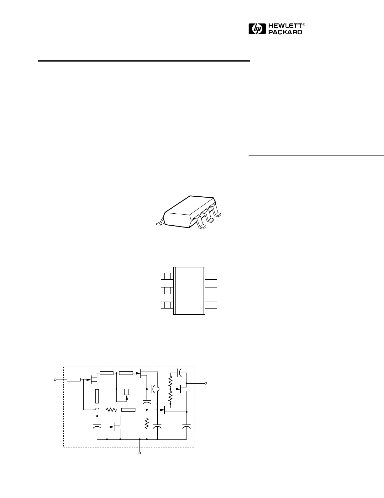
Equivalent Circuit
RF
INPUT
1
GROUND 2, 3, 5, 6
Surface Mount Package SOT-363 (SC-70)
Pin Connections and Package Marking
INPUT
Note:
Package marking provides orientation
and identification.
16
86
GND
25
GND
34
4
RF OUTPUT
AND V
GND
GND
OUTPUT
and V
d
Description
Hewlett-Packard’s MGA-86563 is
an economical, easy-to-use GaAs
MMIC amplifier that offers low
noise figure and excellent gain for
applications from 0.5 to 6 GHz.
Packaged in an ultra-miniature
SOT-363 package, it requires half
the board space of the SOT-143.
The MGA-86563 may be used
without impedance matching as a
high performance 2 dB NF gain
block. Alternatively, with the
addition of a simple shunt-series
inductor at the input, the device
noise figure can be reduced to
1.6␣ dB at 2.4 GHz. For 1.5 GHz
d
applications and above, the
output is well matched to 50 Ω.
Below 1.5 GHz, gain can be
increased by using conjugate
matching.
The circuit uses state-of-the-art
PHEMT technology with selfbiasing current sources, a sourcefollower interstage, resistive
feedback, and on-chip impedance
matching networks. A patented,
on-chip active bias circuit allows
operation from a single +5 V
power supply. Current consumption is only 14 mA, making this
part suitable for battery powered
applications.
5965-9686E
6-220

MGA-86563 Absolute Maximum Ratings
Absolute
Symbol Parameter Units Maximum
V
d
V
in
P
in
T
ch
T
STG
Device Voltage, RF V 9
Output to Ground
RF Input Voltage to V +0.5
Ground –1.0
CW RF Input Power dBm +13
Channel Temperature °C 150
Storage Temperature °C -65 to 150
[1]
Thermal Resistance
θ
= 160°C/ W
ch-c
Notes:
1. Operation of this device above any one
of these limits may cause permanent
damage.
2. T
= 25°C (T
C
temperature at the package pins where
contact is made to the circuit board).
is defined to be the
C
[2]
:
Electrical Specifications, T
= 25°C, ZO = 50 Ω unless noted, V
C
= 5 V
d
Symbol Parameters and Test Conditions Units Min. Typ. Max.
G
NF
NF
test
test
Gain in Test Circuit
Noise Figure in Test Circuit
O
Optimum Noise Figure f = 0.9 GHz dB 2.0
[1]
[1]
f = 2.0 GHz 17 20
f = 2.0 GHz 1.8 2.3
(Tuned for lowest noise figure) f = 2.0 GHz 1.5
f = 2.4 GHz 1.6
f = 4.0 GHz 1.7
f = 6.0 GHz 2.0
G
A
Associated Gain at NF
O
f = 0.9 GHz dB 20.8
(Tuned for lowest noise figure) f = 2.0 GHz 22.7
f = 2.4 GHz 22.5
f = 4.0 GHz 18.0
f = 6.0 GHz 13.7
P
1 dB
Output Power at 1 dB Gain Compression f = 0.9 GHz dBm 3.6
(50 Ω Performance) f = 2.0 GHz 4.1
f = 2.4 GHz 4.2
f = 4.0 GHz 4.3
f = 6.0 GHz 3.3
IP
3
VSWR
VSWR
I
d
Note:
1. Guaranteed specifications are 100% tested in the circuit in Figure 10 in the Applications Information section.
Third Order Intercept Point f = 2.4 GHz dBm +15
Input VSWR f = 2.4 GHz 2.3:1
in
Output VSWR f = 2.4 GHz 1.7:1
out
Device Current mA 14
6-221

MGA-86563 Typical Performance, T
P
1 dB
(dBm)
0
0
FREQUENCY (GHz)
10
4
2
6
8
4
123 5
7.0 V
6
5.5 V
5.0 V
4.5 V
5
30
= 25° C, V
C
= 5 V
d
10
4
3
2
NOISE FIGURE (dB)
1
0
0
2
1
FREQUENCY (GHz)
3
+85
+25
-40
45
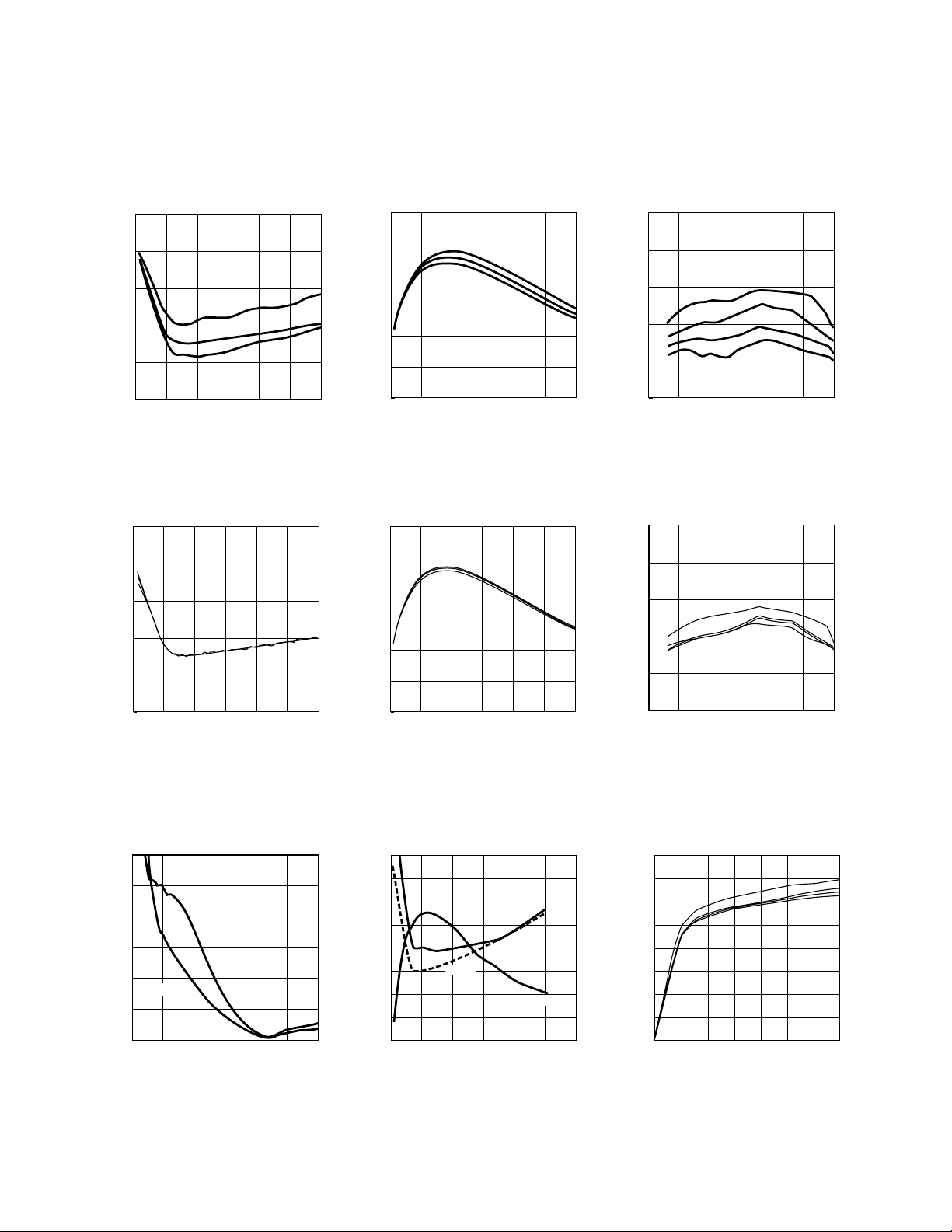
Figure 1. Minimum Noise Figure
(Optimum Tuning) vs. Frequency and
Temperature.
5
4
3
2
NOISE FIGURE (dB)
1
25
20
15
10
ASSOCIATED GAIN (dB)
5
0
0
6
1
3
2
FREQUENCY (GHz)
Figure 2. Associated Gain (Optimum
Tuning) vs. Frequency and
Temperature.
30
25
20
5.5 V
5.0 V
4.5 V
15
10
ASSOCIATED GAIN (dB)
5
45
8
6
-40
(dBm)
+25
+85
6
1 dB
P
-40
4
+25
+50
+85
2
0
0
123 5
FREQUENCY (GHz)
Figure 3. Output Power for 1 dB Gain
Compression (into 50 Ω) vs.
Frequency and Temperature.
5.5 V
5.0 V
4.5 V
4
6
0
0
12 4
FREQUENCY (GHz)
3
5
6
Figure 4. Minimum Noise Figure
(Optimum Tuning) vs. Frequency and
Voltage.
4.0
3.5
3.0
2.5
VSWR (n:1)
2.0
OUTPUT
1.5
1.0
0
Figure 7. Input and Output VSWR
(into 50 Ω) vs. Frequency.
INPUT
3
2
1
FREQUENCY (GHz)
45
6
0
0
1
3
2
FREQUENCY (GHz)
45
Figure 5. Associated Gain (Optimum
Tuning) vs. Frequency and Voltage.
4.0
3.5
3.0
2.5
2.0
1.5
1.0
NOISE FIGURE (dB)
0.5
NF 50
NFopt
GA 50
0
0
4
2
6
FREQUENCY (GHz)
810
Figure 8. 50 Ω Noise Figure and
Associated Gain vs. Frequency.
6
Figure 6. Output Power for 1 dB Gain
Compression (into 50 Ω) vs.
Frequency and Voltage.
32
24
16
8
0
12
16
14
12
10
8
6
CURRENT (mA)
4
ASSOCIATED GAIN (dB)
2
0
0
1
2
3
VOLTAGE (V)
Figure 9. Device Current vs. Voltage.
4
56
-40
+25
+50
+85
7
6-222
 Loading...