

0.1– 6 GHz 3 V, 17 dBm Amplifier
Technical Data
MGA-82563
Features
• +17.3 dBm P
+20 dBm P
• Single +3V Supply
• 2.2 dB Noise Figure at
2.0␣ GHz
• 13.2 dB Gain at 2.0 GHz
• Ultra-miniature Package
• Unconditionally Stable
at 2.0 GHz
1 dB
at 2.0 GHz
sat
Applications
• Buffer or Driver Amp for
PCS, PHS, ISM, SATCOM
and WLL Applications
• High Dynamic Range LNA
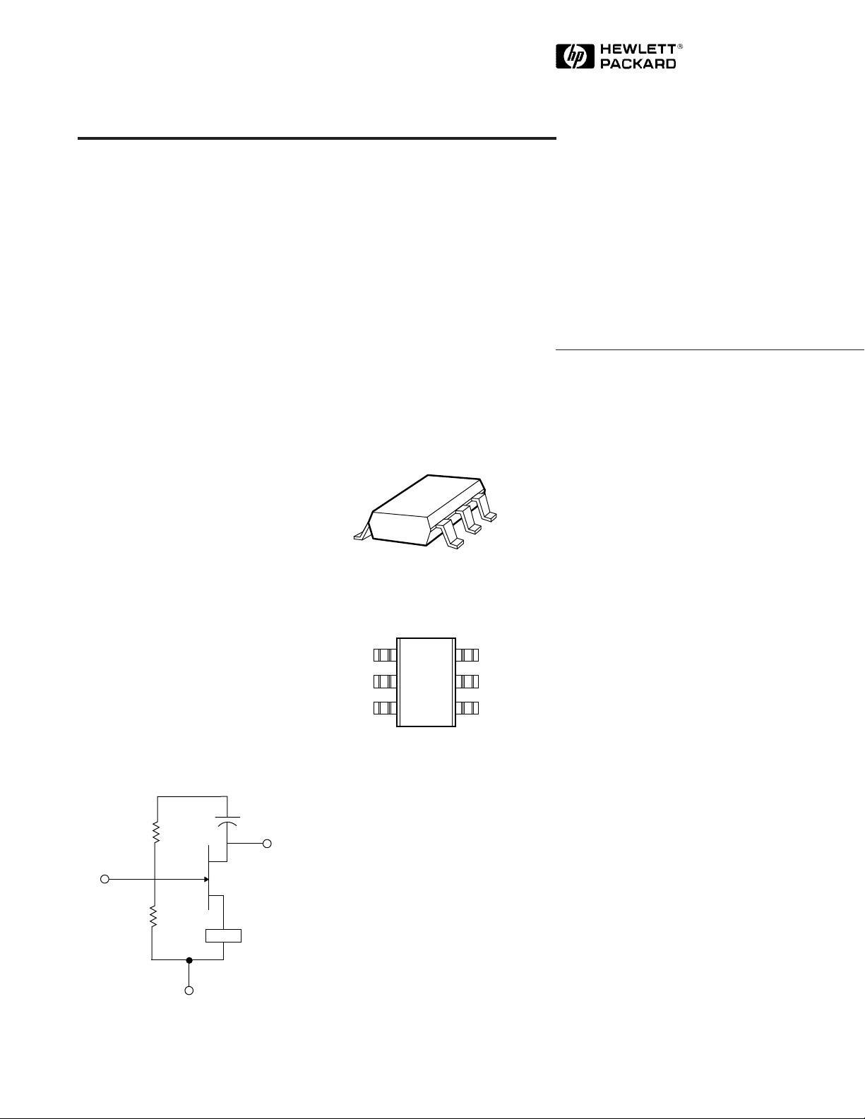
Simplified Schematic
OUTPUT
and V
INPUT
3
6
Surface Mount Package
SOT-363 (SC-70)
Description
Hewlett-Packard’s MGA-82563 is
an economical, easy-to-use GaAs
MMIC amplifier that offers
excellent power and low noise
figure for applications from 0.1 to
6 GHz. Packaged in an ultraminiature SOT-363 package, it
requires half the board space of a
SOT-143 package.
Pin Connections and Package Marking
GND
1
GND
2
INPUT
3
Note: Package marking provides
orientation and identification.
d
82
OUTPUT
6
and V
5
GND
4 GND
The input and output of the
amplifier are matched to 50␣ Ω
(below 2:1 VSWR) across the
d
entire bandwidth, eliminating the
expense of external matching.
The amplifier allows a wide
dynamic range by offering a 2.2 dB
NF coupled with a +31 dBm
Output IP3.
The circuit uses state-of-the-art
PHEMT technology with proven
reliability. On-chip bias circuitry
allows operation from a single
+3␣ V power supply, while resistive
feedback ensures stability (K>1)
over all frequencies and
temperatures.
5965-9685E
GND
1, 2, 4, 5
BIAS
BIAS
6-208
MGA-82563 Absolute Maximum Ratings
Absolute
Symbol Parameter Units Maximum
T
V
V
P
T
V
d
gd
in
in
ch
STG
Device Voltage, RF Output V 5.0
to Ground
Device Voltage, Gate V -6.0
to Drain
Range of RF Input Voltage V +0.5 to -1.0
to Ground
CW RF Input Power dBm +13
Channel Temperature °C 165
Storage Temperature °C - 65 to 150
[1]
Thermal Resistance
θ
= 180°C/W
ch-c
Notes:
1. Permanent damage may occur if
any of these limits are exceeded.
= 25°C (TC is defined to be the
2. T
C
temperature at the package pins
where contact is made to the
circuit board.)
[2]
:
MGA-82563 Electrical Specifications, T
Symbol Parameters and Test Conditions Units Min. Typ. Max. Std Dev
G
NF
NF
test
test
50
Gain in test circuit
Noise Figure in test circuit
Noise Figure in 50 Ω system f = 0.5 GHz dB 2.3
[1]
[1]
= 25° C, ZO = 50 Ω, Vd = 3 V
C
f = 2.0 GHz 12.0 13.2 0.35
f = 2.0 GHz 2.2 2.9 0.20
[2]
f = 1.0 GHz 2.2
f = 2.0 GHz 2.2 0.20
f = 3.0 GHz 2.2
f = 4.0 GHz 2.4
f = 6.0 GHz 2.7
2
|
|S
21
Gain in 50 Ω system f = 0.5 GHz dB 14.7
f = 1.0 GHz 14.5
f = 2.0 GHz 13.5 0.35
f = 3.0 GHz 12.1
f = 4.0 GHz 10.7
f = 6.0 GHz 8.8
P
1 dB
Output Power at 1 dB Gain Compression f = 0.5 GHz dBm 17.4
f = 1.0 GHz 17.5
f = 2.0 GHz 17.3 0.54
f = 3.0 GHz 17.1
f = 4.0 GHz 17.0
f = 6.0 GHz 16.8
IP
VSWR
VSWR
I
Notes:
1. Guaranteed specifications are 100% tested in the circuit in Figure 10 in the Applications Information section.
2. Standard deviation number is based on measurement of at least 500 parts from three non-consecutive wafer lots during
the initial characterization of this product, and is intended to be used as an estimate for distribution of the typical
specification.
Output Third Order Intercept Point f = 2.0 GHz dBm +31 1.0
3
Input VSWR f = 0.2–5.0 GHz 1.8:1
in
Output VSWR f = 0.2–5.0 GHz 1.2:1
out
Device Current mA 63 84 101
d
6-209
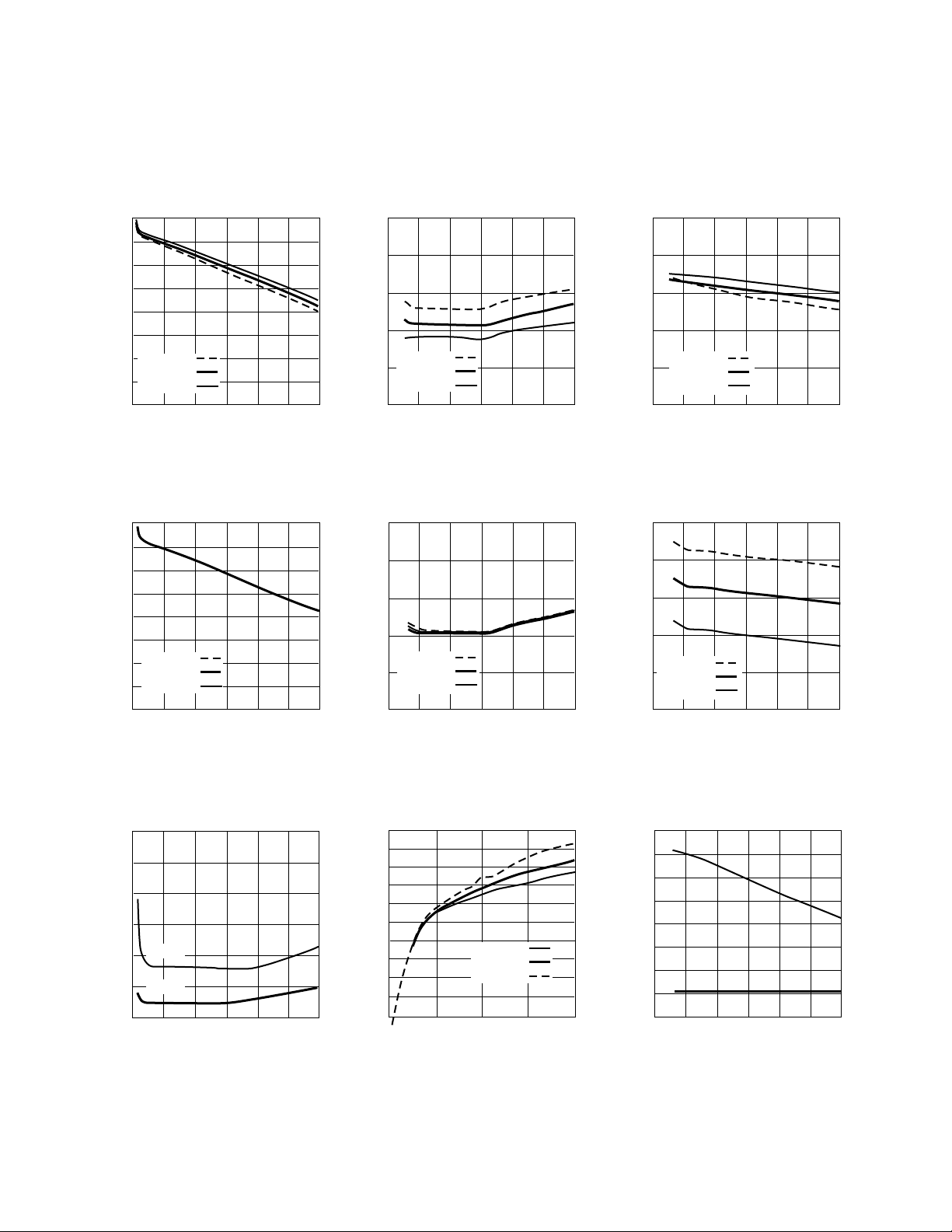
MGA-82563 Typical Performance, T
= 25° C, V
C
= 3 V
d
16
14
12
10
(dB)
8
GAIN
6
4
TA = +85°C
= +25°C
T
A
2
= –40°C
T
A
0
034512 6 0 34512 6
FREQUENCY (GHz) FREQUENCY (GHz)
Figure 1. 50 Ω Power Gain vs.
Frequency and Temperature.
16
14
12
10
(dB)
8
GAIN
6
Vd = 3.3V
4
= 3.0V
V
d
2
= 2.7V
V
d
0
034512 6
FREQUENCY (GHz)
Figure 4. 50 Ω Power Gain vs.
Frequency and Voltage.
5
4
(dB)
3
2
NOISE FIGURE
TA = +85°C
1
= +25°C
T
A
= –40°C
T
A
0
Figure 2. Noise Figure (into 50 Ω)
vs. Frequency and Temperature.
5
4
(dB)
3
2
Vd = 3.3V
NOISE FIGURE
1
= 3.0V
V
d
= 2.7V
V
d
0
034512 6
FREQUENCY (GHz)
Figure 5. Noise Figure (into 50 Ω) vs.
Frequency and Voltage.
19
18
17
(dBm)
1 dB
16
P
TA = +85°C
15
14
= +25°C
T
A
= –40°C
T
A
034512 6
FREQUENCY (GHz)
Figure 3. Output Power @ 1 dB Gain
Compression vs. Frequency and
Temperature.
19
18
17
(dBm)
1 dB
16
P
Vd = 3.3V
15
= 3.0V
V
d
= 2.7V
V
d
14
034512 6
FREQUENCY (GHz)
Figure 6. Output Power @ 1 dB Gain
Compression vs. Frequency and
Voltage.
4
3.5
3
2.5
VSWR (n:1)
Input
2
1.5
Output
1
034512 6
FREQUENCY (GHz)
Figure 7. Input and Output VSWR
into 50 Ω vs. Frequency.
110
100
90
80
(mA)
70
60
50
40
30
DEVICE CURRENT
20
10
03412
TA = +85°C
= +25°C
T
A
= -40°C
T
A
DEVICE VOLTAGE (V)
Figure 8. Device Current vs. Voltage
and Temperature.
6-210
16
14
12
(dB)
10
GAIN and NF
Gain
8
6
4
2
0
NF
034512 6
FREQUENCY (GHz)
Figure 9. Minimum Noise Figure and
Associated Gain vs. Frequency.

MGA-82563 Typical Scattering Parameters
Freq. S
11
S
21
[1]
, T
= 25° C, ZO = 50 Ω, Vd = 3 V
C
S
12
S
22
GHz Mag Ang dB Mag Ang dB Mag Ang Mag Ang Factor
0.1 0.48 -39 15.71 6.10 164 -23 0.070 27 0.16 -99 1.02
0.2 0.35 -35 14.81 5.50 165 -22 0.076 14 0.12 -134 1.20
0.5 0.29 -37 14.34 5.21 159 -22 0.079 6 0.11 177 1.29
1.0 0.29 -57 13.95 4.98 144 -22 0.080 3 0.11 156 1.33
1.5 0.29 -78 13.50 4.73 128 -22 0.082 2 0.10 142 1.37
2.0 0.29 -99 12.99 4.46 114 -22 0.085 1 0.10 131 1.41
2.5 0.29 -118 12.45 4.19 99 -21 0.089 -1 0.10 124 1.44
3.0 0.28 -138 11.84 3.91 86 -21 0.093 -3 0.11 118 1.48
3.5 0.28 -158 11.24 3.65 74 -21 0.098 -6 0.12 111 1.51
4.0 0.29 -177 10.67 3.42 61 -20 0.103 -9 0.13 106 1.52
4.5 0.30 166 10.11 3.20 50 -20 0.107 -13 0.15 100 1.53
5.0 0.32 151 9.58 3.01 38 -19 0.112 -18 0.16 94 1.54
5.5 0.34 136 9.07 2.84 27 -19 0.117 -23 0.18 87 1.55
6.0 0.36 123 8.57 2.68 16 -19 0.121 -29 0.19 82 1.54
6.5 0.38 110 8.06 2.53 5 -19 0.125 -35 0.22 74 1.55
7.0 0.40 97 7.51 2.37 -5 -18 0.126 -41 0.24 66 1.59
K
MGA-82563 Typical Noise Parameters
[1]
TC = 25° C, ZO = 50 Ω, Vd = 3 V
Frequency NF
O
Γ
opt
GHz dB Mag. Ang. —
0.5 2.10 0.15 25 1.20
1.0 2.10 0.15 45 0.60
1.5 2.10 0.14 65 0.29
2.0 2.12 0.15 75 0.27
2.5 2.12 0.15 94 0.25
3.0 2.15 0.144 113 0.23
3.5 2.16 0.14 134 0.21
4.0 2.16 0.15 155 0.19
4.5 2.19 0.17 177 0.18
5.0 2.18 0.20 -166 0.18
5.5 2.19 0.22 -152 0.18
6.0 2.23 0.25 -138 0.19
6.5 2.28 0.27 -125 0.23
7.0 2.39 0.29 -111 0.28
Note:
1. Reference plane per Figure 11 in Applications Information section.
R
/ 50 Ω
n
6-211
 Loading...