HP HMMC-5023DC, HMMC-5023RF Datasheet

6-34
23 GHz LNA
(21.2 – 26.5 GHz)
Technical Data
Features
• Frequency Range:
21 .2 – 23.6 GHz and
24.5 – 26.5 GHz Specified
21 – 30 GHz Performance
• Low Noise Temperature:
226 K (2.5 dB N.F.) Typical
• High Gain: 24 dB Typical
• 50 Ω Input/Output Matching
• Single Supply Bias with
Optional Bias Adjust:
5 volts (@ 24 mA Typical)
Description
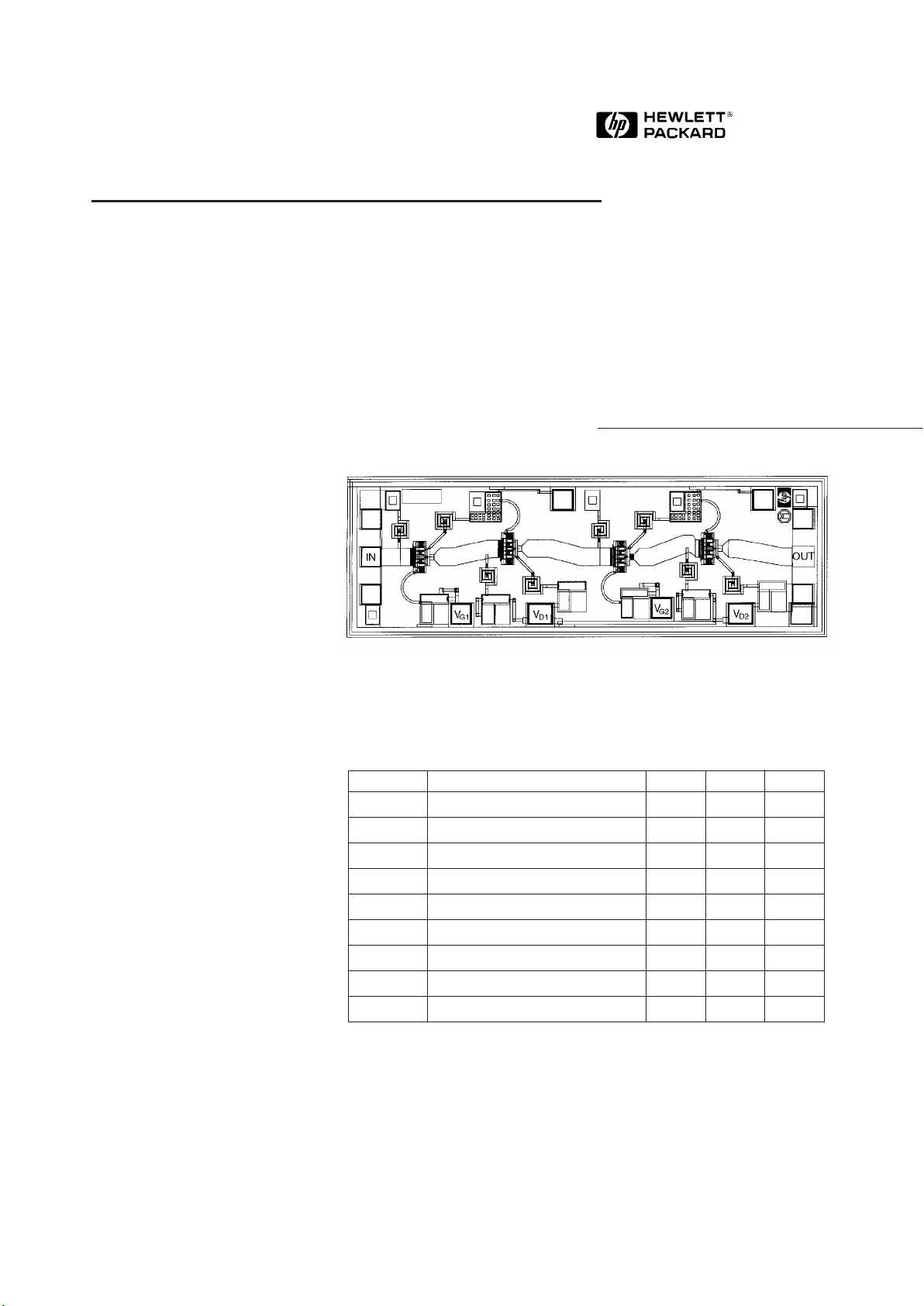
The HMMC-5023 MMIC is a highgain low-noise amplifier (LNA)
that operates from 21 GHz to over
30 GHz. By eliminating the
complex tuning and assembly
processes typically required by
hybrid (discrete-FET) amplifiers,
the HMMC-5023 is a cost-effective
alternative in 21.2 – 23.6 GHz and
24.5 – 26.5 GHz communications
receivers. The device has good
input and output match to
50␣ ohms and is unconditionally
stable to more than 40 GHz. The
backside of the chip is both RF
and DC ground. This helps
simplify the assembly process
and reduces assembly related
performance variations and costs.
It is fabricated using a PHEMT
integrated circuit structure that
provides exceptional noise and
gain performance.
Absolute Maximum Ratings
[1]
Symbol Parameters/Conditions Units Min. Max.
VD1, V
D2
Drain Supply Voltage V 3 8
VD1, V
D2
Gate Supply Voltage V 0.4 2
I
D1
Drain Supply Current mA 35
I
D2
Drain Supply Current mA 35
P
in
RF Input Power
[2]
dBm 15
T
ch
Operating Channel Temp.
[3]
°C +150
T
A
Backside Ambient Temp. °C -55 +140
T
STG
Storage Temperature °C - 65 +165
T
max
Maximum Assembly Temp. °C +300
Notes:
1. Absolute maximum rating for continuous operation unless otherwise noted.
2. Operating at this power level for extended (continuous) periods is not
recommended.
3. Refer to DC Specifications/Physical Properties table for derating information.
Chip Size: 2980 x 620 µm (74 x 24.4 mils)
Chip Size Tolerance: ± 10 µm (± 0.4 mils)
Chip Thickness: 127 ± 15 µm (5.0 ± 0.6 mils)
Pad Dimensions: 80 x 80 µm (3.1 x 3.1 mils), or larger
HMMC-5023
5965-5448E

6-35
HMMC-5023 DC Specifications/Physical Properties
[1]
Symbol Parameters and Test Conditions Units Min. Typ. Max.
VD1, V
D2
Recommended Drain Supply Voltage V 3 5 7
VG1, V
G2
Gate Supply Voltage V 0.4 0.8
[2]
2
[VD1 ≤ VD1(max), V
D2
≤ V
D2
(max)]
ID1, I
D2
Input and Output Stage Drain Supply Current mA 12 35
(VG1 = VG2 = Open, VD1 = VD2 = 5 Volts)
ID1 + I
D2
Total Drain Supply Current mA 13 24 30
(VG1 = VG2 = Open, VD1 = VD2 = 5 Volts)
θ
ch-bs
Thermal Resistance
[3]
° C/Watt 75
(Channel-to-Backside at T
ch
= 150° C)
T
ch
Channel Temperature
[4]
(T
A
= 140° C, MTTF = 106 hrs, °C 150
V
G1
= VG2 = Open, V
D1
= VD = 5 Volts)
Notes:
1. Backside ambient operating temperature T
A
= 25°C unless otherwise noted.
2. Open circuit voltage at VG1 and VG2 when VD1 and VD2 are 5 volts.
3. Thermal resistance (in °C/Watt) at a channel temperature T (°C) can be estimated using this equation:
θ(T) @ 75 x [T(°C)+ 273] / [150°C+ 273].
4. Derate MTTF by a factor of two for every 8°C above T
ch
.
HMMC-5023 RF Specifications,
T
op
= 25°C, V
D1
= V
D2
= 5 V, VG1 = VG2= Open, Z
O
= 50 Ω, unless otherwise noted
21.2–23.6 GHz 24.5–26.5 GHz
Symbol Parameters and Test Conditions Units Min. Typ. Max. Min. Typ. Max.
BW Operating Bandwidth GHz 21.2 23.6 24.5 26.5
Gain Small Signal Gain dB 21 24 28 17 21 25
∆ Gain Small Signal Gain Flatness dB ±1 ±1.5
(RLin)
MIN
Minimum Input Return Loss dB 10 12 12 20
(RL
out)MIN
Minimum Output Return Loss dB 8 10 8 10
Isolation Reverse Isolation dB 40 50 40 48
Output Power @ 1 dB Gain Compression dBm 10 10
P
-1dB
Output Power @ 1 dB Gain Compression dBm 14 14
(VD = 5 V, VG1= Open, VD2 = 7 V,
VG2 set for ID2 = 35 mA)
P
sat
Saturated Output Power dBm 12 12
(@ 3 dB Gain Compression)
2nd Harm. Second Harmonic Power Level dBc -30 -30
[f = 2 fo, P
out
(fo) = P
-1dB
,
21.2 GHz ≤ fo ≤ 23.6 GHz]
NF
Noise Figure, 22 GHz
dB
2.5 3.0
Noise Figure, 25 GHz 2.8 3.3
 Loading...