

Page 1

Artisan Technology Group is your source for quality
new and certied-used/pre-owned equipment
• FAST SHIPPING AND
DELIVERY
• TENS OF THOUSANDS OF
IN-STOCK ITEMS
• EQUIPMENT DEMOS
• HUNDREDS OF
MANUFACTURERS
SUPPORTED
• LEASING/MONTHLY
RENTALS
• ITAR CERTIFIED
SECURE ASSET SOLUTIONS
SERVICE CENTER REPAIRS
Experienced engineers and technicians on staff
at our full-service, in-house repair center
Instra
Remotely inspect equipment before purchasing with
our interactive website at www.instraview.com
Contact us: (888) 88-SOURCE | sales@artisantg.com | www.artisantg.com
SM
REMOTE INSPECTION
View
WE BUY USED EQUIPMENT
Sell your excess, underutilized, and idle used equipment
We also offer credit for buy-backs and trade-ins
www.artisantg.com/WeBuyEquipment
LOOKING FOR MORE INFORMATION?
Visit us on the web at www.artisantg.com for more
information on price quotations, drivers, technical
specications, manuals, and documentation
Page 2

Contents
HP E1459A 64-Channel Isolated Inpu t Inter rupt Modu le
Edition 3
Warranty .......................................................................................................................5
Safety Symbols .............................................................................................................6
WARNINGS.................................................................................................................6
Declaration of Conformity............................................................................................7
Reader Comment Sheet ................................................................................................9
Chapter 1
Installing and Configuring the HP E1459A ..............................................................11
Functional Description................................................................................................11
Watchdog Timer ..................................................................................................14
Input Level Selection ..........................................................................................14
Input Isolation .....................................................................................................14
Input Debounce Processing .................................................................................14
Input Edge Detection ...........................................................................................15
Input Data Capture ..............................................................................................17
Front Panel Markers ............................................................................................18
Interrupt Driven or Polled Mode Operations ......................................................18
Interrupt Parsing ..................................................................................................18
Configuring for Installation ........................................................................................19
Setting the Logical Address ................................................................................20
Setting the Interrupt Priority ...............................................................................20
Setting Input Threshold Levels ................................................... ......... ......... ......21
Setting the Reset Time on the Watchdog Timer .................................................21
Connecting User Inputs .......................................................................................22
Installing the HP E1459A in a VXIbus Mainframe ............................................24
Terminal Block ....................................................................................................25
Wiring a Terminal Block .....................................................................................26
Chapter 2
Using the HP E1459A Module ................................. ......... ......... .................................29
Power-on / Reset States ..............................................................................................30
Example 1: Reset, Self Test, and Module ID ......................................................30
Example 2: Digital Input .....................................................................................32
Edge Detected Event Detection..................................................................................34
Example 3: Edge Interrupt ..................................................................................37
Contents 1
Artisan Technology Group - Quality Instrumentation ... Guaranteed | (888) 88-SOURCE | www.artisantg.com
Page 3

Chapter 3
HP E1459A SCPI Command Reference ....................................................................39
DIAGnostic:SYSReset Subsystem.............................................................................41
DIAGnostic:SYSReset[:STATe]? .......................................................................41
DIAGnostic:SYSReset:ENABle <state> ............................................................41
DIAGnostic:SYSReset:ENABle? .......................................................................42
DISPlay:MONitor Subsystem.....................................................................................43
DISPlay:MONitor:PORT <port> ........................................................................43
DISPlay:MONitor:PORT? [MINimum | MAXimum | DEFault] .................. ......44
DISPlay:MONitor:PORT:AUTO <state> ...........................................................44
DISPlay:MONitor:PORT:AUTO? ...................................................................... 44
DISPlay:MONitor[:STATe] <state> ...................................................................45
DISPlay:MONitor[:STATe]? .............................................................................. 45
INPut Subsystem.........................................................................................................46
INPutn:CLOCk[:SOURce] <source> ..................................................................46
INPutn:CLOCk[:SOURce]? ................................................................................47
INPutn:DEBounce:TIME <time> | MINimum | MAXimum | DEFault .............47
INPutn:DEBounce:TIME? [MINimum | MAXimum | DEFault] ....................... 48
MEASure Subsystem..................................................................................................49
MEASure:DIGital:DATAn[:type] [:VALue]? ....................................................49
MEASure:DIGital:DATAn[:type]:BITm? .......................................................... 50
MEMory Subsystem ............................................................................................. ......51
MEMory:DELete:MACRo <name> ...................................................................51
SENSe Subsystem.......................................................................................................52
[SENSe:]EVENt:PORTn:DAVailable? .............................................................. 52
[SENSe:]EVENt:PORTn:DAVailable:ENABle <state> ....................................53
[SENSe:]EVENt:PORTn:DAVailable:ENABle? ...............................................53
[SENSe:]EVENt:PORTn:EDGE? ....................................................................... 54
[SENSe:]EVENt:PORTn:EDGE:ENABle <state> .............................................54
[SENSe:]EVENt:PORTn:EDGE:ENABle? ........................................................ 55
[SENSe:]EVENt:PORTn:NEDGe? .....................................................................55
[SENSe:]EVENt:PORTn:NEDGe:ENABle <mask> ..........................................56
[SENSe:]EVENt:PORTn:NEDGe:ENABle? ......................................................5 6
[SENSe:]EVENt:PORTn:PEDGe? .....................................................................57
[SENSe:]EVENt:PORTn:PEDGe:ENABle <mask> ..........................................57
[SENSe:]EVENt:PORTn:PEDGe:ENABle? ......................................................58
[SENSe:]EVENt:PSUMmary:DAVailable? .......................................................58
[SENSe:]EVENt:PSUMmary:EDGE? ................................................................ 59
STATus Subsystem.....................................................................................................60
STATus:OPERation:CONDition? ......................................................................62
STATus:OPERation:ENABle <mask> ...............................................................62
STATus:OPERation:ENABle? ...........................................................................63
STATus:OPERation[:EVENt]? ...........................................................................63
STATus:OPERation:PSUMmary:CONDition? .................................................. 63
STATus:OPERation:PSUMmary:ENABle <mask> ...........................................64
STATus:OPERation:PSUMmary:ENABle? ....................................................... 64
STATus:OPERation:PSUMmary[:EVENt]? ......................................................65
STATus:PRESet ..................................................................................................6 5
2 Contents
Artisan Technology Group - Quality Instrumentation ... Guaranteed | (888) 88-SOURCE | www.artisantg.com
Page 4

STATus:QUEStionable:CONDition? .................................................................66
STATus:QUEStionable:ENABle <mask> ..........................................................66
STATus:QUEStionable:ENABle? ......................................................................67
STATus:QUEStionable[:EVENt]? ......................................................................67
SYSTem Subsystem ....................................... ...................................................... ......68
SYSTem:CDEScription? <number> ...................................................................68
SYSTem:CTYPe? <number> ..............................................................................68
SYSTem:ERRor? ................................................................................................ 69
SYSTem:VERSion? ............................................................................................ 69
IEEE 488.2 Common Commands...............................................................................7 0
Command Quick Reference........................................................................................71
Appendix A
HP E1459A Specifications ...........................................................................................73
Appendix B
HP E1459A Register Definitions ................................................................................75
Overview.....................................................................................................................75
Addressing the Registers ............................................................................................76
Register Access with Logical Address ................................................................76
Register Access with Memory Mapping .............................................................76
Register Definitions....................................................................................................77
Manufacturer ID Register ..................................................................... ......... ......78
Device Type Register .................................................................. ......... ......... ......78
Status/Control Register .......................................................................................78
Edge Interrupt Status Register .............................................................................80
Data Available Status Register ......................... ...................................................80
Watchdog Timer Control/Status Regist er ...........................................................81
Command Register Port 0/2 ................................................................................81
Channel Data Register Port 0/2 ...........................................................................83
Positive Edge Detect Register Port 0/2 ...............................................................83
Negative Edge Detect Register Port 0/2 ..............................................................84
Positive Mask Register Port 0/2 ..........................................................................84
Negative Mask Register Port 0/2 ........................................................................84
Debounce Clock Register Port 0 and Port1/ Port 2 and Port 3 ...........................85
Command Register Port 1/3 ................................................................................86
Channel Data Register Port 1/3 ...........................................................................87
Positive Edge Detect Register Port 1/3 ...............................................................88
Negative Edge Detect Register Port 1/3 ..............................................................88
Positive Mask Register Port 1/3 ..........................................................................88
Negative Mask Register Port 1/3 ........................................................................89
Debounce Clock Register Port 0 and Port 1/ Port 2 and Port 3 ..........................89
Power On/Reset Conditions........................................................................................91
Programming Examples..............................................................................................91
Output and Edge Detection Examples ................................................................92
Appendix C
Error Messages ..........................................................................................................105
Contents 3
Artisan Technology Group - Quality Instrumentation ... Guaranteed | (888) 88-SOURCE | www.artisantg.com
Page 5

4 Contents
Artisan Technology Group - Quality Instrumentation ... Guaranteed | (888) 88-SOURCE | www.artisantg.com
Page 6

Certification
Hewlett-Packard Company certifies that this product met its published specifications at the time of shipment from the factory. HewlettPackard further certifies that its calibration measurements are traceable to the United Sta tes Nati onal Insti tute of Sta ndards and
Technology (formerly National Bureau of Standards), to the extent allowed by that organization's calibration facility, and to t he
calibration facilities of other International Standards Organization members.
Warranty
This Hewlett-Packard product is warranted against defects in materials and workmanship for a period of three years from date of shipment.
Duration and conditions of warrant y for th is product ma y be superseded when the product is integrated in to (becomes a part of) other HP
products. During the warranty period, Hewlett-Packard Company will, at its option, either repair or replace products which prove to be
defective.
For warranty service or repair, this product must be returned to a service facility designated by Hewlett-Packard (HP). Buyer s hall prep ay
shipping charges to HP and HP shall pay shipping charges to return the product to Buyer. However, Buyer shall pay all shipping charges,
duties, and taxes for products returned to HP from another country
HP warrants that its software and firmware designated by HP for use with a product will execute its programming instructions when
properly installed on that product. HP does not warrant that the operation of the product, or software, or firmware will be uninterrupted
or error free.
Limitation Of Warranty
The foregoing warranty shall not appl y to defects resulting fro m improper or inad equate maintenance b y Buyer, Buyer-suppl ied prod ucts
or interfacing, unauthorized modification or misuse, operation outside of the environmental specifications for the product, or improper
site preparation or maintenance.
The design and implementation of any circuit on this product is the sole responsibility of the Buyer. HP does not warrant the Buyer's
circuitry or malfunctions of HP products that result from the Buyer's circuitry. In addition, HP does not warrant any damage that occurs
as a result of the Buyer's circuit or any defects that result from Buyer-supplied products.
NO OTHER WARRANTY IS EXPRESSED OR IMPLIED. HP SPECIFICALLY DISCLAIMS THE IMPLIED WARRANTIES OF
MERCHANTABILITY AND FITNESS FOR A PARTICULAR PURPOSE.
Exclusive Remedies
THE REMEDIES PROVIDED HEREIN ARE BUYER 'S SO LE AND EXC LUSIVE REM EDIES. HP SHALL NOT BE LIABLE FOR
ANY DIRECT, INDIRECT, SPECIAL, INCIDENTAL, OR CONSEQUENTIAL DAMAGES, WHETHER BASED ON CONTRACT,
TORT, OR ANY OTHER LEGAL THEORY.
Notice
The information contained in this document is subject to change without notice. HEWLETT-PACKARD (HP) MAKES NO
WARRANTY OF ANY KIND WITH REGARD TO THIS MATERIAL, INCLUDING, BUT NOT LIMITED TO, THE IMPLIED
WARRANTIES OF MERCHANTABILITY AND FITNESS FOR A PARTICULAR PURPOSE. HP shall not be liable for errors
contained herein or for incidental or consequenti al damages in connection with the furnish ing, performance or use of this material. This
document contains proprietary information which is protected by copyright. All rights are reserved. No part of this document may be
photocopied, repro duced , o r tran slated t o an oth er lan gu age with out the prior written consent of Hewlett-Packard Company. HP assumes
no responsibility for the use or reliability of its software on equipment that is not furnished by HP.
U.S. Government Restricted Rights
The Software and Documentation have been developed entirely at private expense. They are delivered and licensed as "commercial
computer software" as defined in DFARS 252.227- 7013 (Oct 1988), DFARS 252.211-7015 (May 1991) or DFARS 252.227-7014 (Jun
1995), as a "commercial item" as defined in FAR 2.101(a), or as "Restricted computer software" as defined in FAR 52.227-19 (Jun
1987)(or any equivalent agency regulation or contract clause), whichever is applicable. You have only those rights provided for such
Software and Documentation by the applicable FAR or DFARS clause or the HP standard software agreement for the product involved
HP E1459A / Z2404B 64-Channel Isolated Input / Interrupt Module User's Manual
Edition 3
Copyright © 1997 Hewlett-Packard Company. All Rights Reserved.
Artisan Technology Group - Quality Instrumentation ... Guaranteed | (888) 88-SOURCE | www.artisantg.com
5
Page 7

Documentation History
All Editions and Updates of this manual and their creation date are listed below. The first Edi tion of the manu al is Editi on 1. The Edition
number increments by 1 whenever the manual is revised. Updates, which are issued between Editions, contain replacement pages to
correct or add additional information to the current Edition of the manual. Whenever a new Edition is created, it will contain all of the
Update information for the p revious Edition . Each new Editi on or Update also includ es a revised copy of th is documentation histor y page.
Edition 1 (as HP Z2404-90000). . . . . . . . . . . . . . . . . . . . . . . . . . . . August 1991
Edition 2 (as HP Z2404-90001). . . . . . . . . . . . . . . . . . . . . . . . . . . February 1996
Edition 3 (HP E1459-90001). . . . . . . . . . . . . . . . . . . . . . . . . . . . . . . . .July 1997
Safety Symbols
Instruction manual s ymbol affi xed to
Instruction manual s ymbol affi xed to
product. Indicates that the user must refer to
product. Indicates that the user must refer to
the manual for specific WARNING or
the manual for specific WARNING or
CAUTION information to avoid personal
CAUTION information to avoid personal
injury or damage to the product.
injury or damage to the product.
Indicates the field wiring terminal that must
be connected to earth ground before
operating the equipment — protects against
electrical shock in case of fault.
WARNING
Alternating current (AC)
Direct current (DC).
Indicates hazardous voltages.
Calls attention to a procedure, practice, or
condition that could cause bodily injury or
death.
or
Frame or chassis ground terminal—typically
connects to the equipment's metal frame.
CAUTION
Calls attention to a procedure, practice, or
condition that could possibl y cause damage to
equipment or permanent loss of data.
WARNINGS
The following general safety precautions must be observed during all phases of operation, service, and repair of this product. Failure to
comply with these precautions or with specific warnings elsewhere in this manual violates safety standards of design, manufacture, and
intended use of the product. Hewlett-Pa ckard Company assumes no liability for th e customer's failure to comply with these require ments.
Ground the equipment: For Safety Class 1 equipment (equipment having a protective earth terminal), an uninterruptible safety earth
ground must be provided from the mains power source to the product input wiring terminals or supplied power cable.
DO NOT operate the product in an explosive atmosphere or in the presence of flammable gases or fumes.
For continued protection against fir e, replace th e lin e fuse(s) on l y with fuse(s) of the same volt age and curren t rating and type. DO NOT
use repaired fuses or short-circuited fuse holders.
Keep away from live circuits: Operating personnel must not remove equipment covers or shields. Procedu res in volving th e removal of
covers or shields are for use by service-trained personnel only. Under certain conditions, dangerous voltages may exist even with the
equipment switched off. To avoid dangerous electrical shock, DO NOT perform procedures involving cover or shield removal unless you
are qualified to do so.
DO NOT operate damaged equipment: Whenever it is possible that the safety protection features built into this product have been
impaired, either through physical damage, excessive moisture, or any other reason, REMOVE POWER and do not use the product until
safe operation can be verified by service-trained personnel. If necessary, return the product to a Hewlett-Packard Sales and Service Office
for service and repair to ensure that safety features are maintained.
DO NOT service or adjust alone: Do not attempt internal service or adjustment unless another person, capable of rendering first aid and
resuscitation, is present.
DO NOT substitute parts or modify equipment: Because of the danger of introd ucing ad ditional h azards, do not install subst itute parts
or perform any unauthorized modification to the product. Return the product to a Hewlett-Packard Sales and Service Office for service
and repair to ensure that safety features are maintained.
6
Artisan Technology Group - Quality Instrumentation ... Guaranteed | (888) 88-SOURCE | www.artisantg.com
Page 8

Declaration of Conformity
according to ISO/IEC Guide 22 and EN 45014
Manufacturer's Name: Hewlett-Packard Company
Loveland Manufacturing Center
declares, that the product:
Product Name: 64-Channel Isolated Digital Input / Interrupt Module
Model Number: HP E1459A (formerly HP Z2404B)
Product Options: All
conforms to the following Product Specifications:
Safety: IEC 1010-1 (1990) Incl. Amend 1 (1992)/EN61010-1/A2 (1995)
CSA C22.2 #1010.1 (1992)
UL 3111
EMC: CISPR 11:1990/EN55011 (1991): Group1 Class A
EN50082-1:1992
IEC 801-2:1991: 4kVCD, 8kVAD
IEC 801-3:1984: 3 V/m
IEC 801-4:1988 : 1kV Power Line
ENV50141:1993/prEN50 082-1 (1995): 3Vrms
ENV50142:1994/prEN50082-1 (1995): 1kV CM, 0.5kV DM
IEC1000-4-8:1993/prEN50082-1 (1995): 3A/m
EN61000-4-11:1994/prEN50082-1 (1995):30%, 10ms 60%, 100ms
Supplementary Information: The product herewith complies with the requirements of the Low Voltage Directive
73/23/EEC and the EMC Directive 89/336/EEC (inclusive 93/68/EEC) and carries the "CE" mark accordingly.
Tested in a typical configuration in an HP C-Size VXI mainframe.
April, 1996
Jim White, QA Manager
European contact: Your local Hewlett-Packard Sales and Service Office or Hewlett-Packard GmbH, Department HQ-TRE, Herrenberger Straße 130, D-71034 Böblingen, Germany (FAX +49-7031-14-3143)
Artisan Technology Group - Quality Instrumentation ... Guaranteed | (888) 88-SOURCE | www.artisantg.com
7
Page 9

Notes:
8
Artisan Technology Group - Quality Instrumentation ... Guaranteed | (888) 88-SOURCE | www.artisantg.com
Page 10

Please fold and tape for mailing
Reader Comment Sheet
HP E1459A / Z2404B 64-Channel Isolated Input / Interrupt Module User’s Manual
Edition 3
You can help us improve our manuals by sharing your comments and suggestions. In appreciation of your ti me, we will
enter you in a quarterly drawing for a Hewlett-Packard Palmtop Personal Computer (U.S. government employees
are not eligible for the drawing).
Your Name
Company Name
Job Title
Address
City, State/Province
Country
Zip/Postal Code
Telephone Number with Area Code
Please list the system controller, operating system, programming language, and plug-in modules you are using.
fold here
BUSINESS REPLY MAIL
FIRST CLASS PERMIT NO. 37 LOVELAND, CO
POSTAGE WILL BE PAID BY ADDRESSEE
cut along this li ne
HEWLETT-PACKARD COMPANY
Measurement Systems Division
Learning Products Department
P.O. Box 301
Loveland, CO 80539-9984
NO POSTAGE
NECESSARY
IF MAILED
IN THE
UNITED STATES
fold here
Please pencil-in one circle for each statement below: Disagree Agree
• The documentation is well organized. OOOOO
Instructions are easy to understand. OOOOO
•
The documentation is clearly written. OOOOO
•
•Examples are clear and useful. OOOOO
Illustrations are clear and helpful. OOOOO
•
The documentation meets my overall expectations. OOOOO
•
Please write any comments or suggestions below–be specific.
Artisan Technology Group - Quality Instrumentation ... Guaranteed | (888) 88-SOURCE | www.artisantg.com
Page 11

Artisan Technology Group - Quality Instrumentation ... Guaranteed | (888) 88-SOURCE | www.artisantg.com
Page 12

Chapter 1
Installing and Configuring the HP E1459A
The HP E1459A 64-Channel Isolated Digital Input/Interrupt module
(formerly known as the HP Z2404B
channels configured as four 16-bit ports. The module is used for sensing
signals and detecting edge changes on digital inputs. The module is a C-Size
VXIbus register-based product that operates in a C-Size VXIbus mainframe.
Each isolated channel can withstand up to 115 Vac RMS or 115 Vdc
difference in ground potential between channels. The input threshold for
each channel is selectable with a jumper to allow for inputs with high logic
levels from 5 to 48 volts. Each channel can be individually masked to
generate an interrupt on a positive and/or negative edge transition. Channel
inputs are also "debounced" to help prevent erroneous transition detection
on noisy signals. Two programmable clock sources control the debounce
circuitry (one for ports 0 and 1, one for ports 2 and 3).
Functional Descriptio n
The HP E1459A simultaneously monitors each channel for the occurrence
of transitions, (i.e., edge events), or for level sensing signals which meet
preprogrammed parameters for magnitude and duty. Each channel is
electrically isolated from all other channels, power, ground, and other
current paths within the limits of specification. Each channel may be
independently programmed to sense only positive transitions, only negative
transitions, or transitions of either polarity.
1
) provides 64 isolated digital input
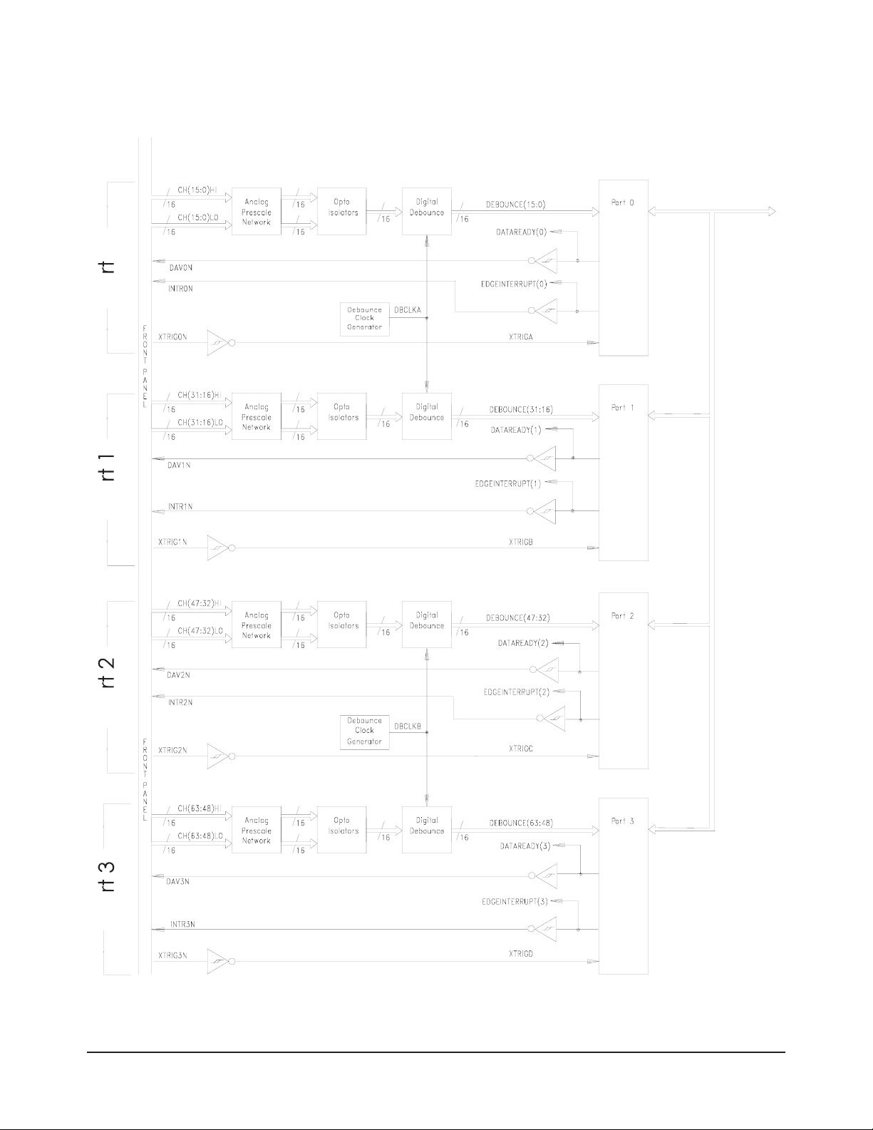
Figure 1-1 shows the functional block diagram for the module.
1. The HP E1459A and Z2404B are functionally identical. The HP E1459A is provided with a downloadable
SCPI driver and a VXIplug&play driver; the HP Z2404B was not provided with a language driver.
Installing and Configuring the HP E1459A 11
Artisan Technology Group - Quality Instrumentation ... Guaranteed | (888) 88-SOURCE | www.artisantg.com
Page 13
To VXIbus
Transceivers
Figure 1-1. HP E1459A 64-Channel Isolated Digital Input/Interrupt Block Diagram
12 Installing and Configuring the HP E1459A
Artisan Technology Group - Quality Instrumentation ... Guaranteed | (888) 88-SOURCE | www.artisantg.com
Page 14
The HP E1459A can be pr ogrammed to mon it or ch annel o ccurren ces ei th er
internally with a 1.0 MHz sample clock, or externally, with a sourced
capture clock. Using either clocking technique, data channels may function
as edge detect inputs and/or data capture inputs.
Events at any channel may occur simultaneously or in overlap with events
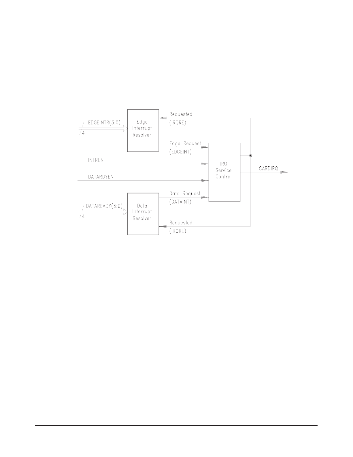
on any other channel. Figure 1-2 is a block diagram of the hardware interrupt
resolver circuit. User software algorithms are also necessary to resolve
issues of overlap and to determine the occurring sequence of events.
Figure 1-2. Resolver Block Diagram
Installing and Configuring the HP E1459A 13
Artisan Technology Group - Quality Instrumentation ... Guaranteed | (888) 88-SOURCE | www.artisantg.com
Page 15

Wa tchdog Time r The HP E1459A prov ides a progr ammable timer f acilit y which, in the e vent
of time-out, will generate a "system wide" reset to all other card-cage
modules. This timer may be disabled by the SCPI command
DIAG:SYSR:ENAB OFF.
Input Level
Selection
Each channel is capable of op eration over an input range from 2.0 through
60.0 Vdc. Input voltages are grouped into vo ltage ranges which ar e selected
via a series of jumpers on the module. These jumpers are described in more
detail beginning on page 21.
Input Isolation Each channel is optically coupled and electrically isolated from all other
channels and current paths. Isolated channel inputs are polarized and require
that the user observe input signal polarity when connections are made.
Input Debounce
Processing
Programmable
Debounce Parameters
Each channel is debounced b y a digital circuit specific to this function. Two
programmable clock sources establish reference parameters which
determine the debounce criteria for validating inputs. Channels are not
independently programmed for debounce period, but are instead grouped
together in blocks of 32 channels per clock source. Channels 00-31 (Ports 0
and 1) are collectively programmed via one clock sou rce and channels 32-63
(Ports 2 and 3) are programmed via a second clock source.
Debounce circuits require that a channel input remain in a stable state for 4
to 4.5 periods of the programmable clock before a channel transition is
declared. The debounce clocks may be programmed for frequencies ranging
from 250 KHz down t o 466 µHz. The 4 to 4.5 clock period requirements of
the debouncers translate into debounce periods which range from 16 µS
minimum to 9600 seconds (2.67 hours) maximum.
The debounce circuits can add considerable latency in the signal path and an
additional delay occurs within the Register FPGA. Normally the signals pass
though without significant delay. However, during a VXIbus transaction to
this port, the input signals are momentarily captured by a latch and are held
for the duration of the bus transaction plus 500 nS. This prevents data events
from being lost due to potential timing conflicts with VXIbus transactions.
The data signals are then synchronized with the system clock and
synchronously captured in either the data register, the positive edge event
register, or the negative edge event register. This can potentiall y add another
500 nS depending upon timing circumstances.
Thus the input data is delayed by the debounce circuits, possibly by the input
latches (equal to bus transaction time plus 500 nS), and a synchronizing
delay of 500 nS. The external clocks (front panel external trigger inputs) are
also delayed but by no more than 500 nS. Therefore, an external capture
clock concurrent with a data event will not capture the event unless
consideration is given for data latency.
14 Installing and Configuring the HP E1459A
Artisan Technology Group - Quality Instrumentation ... Guaranteed | (888) 88-SOURCE | www.artisantg.com
Page 16

Caution The user MUST ensure, based upon the programmed debounce
period and internal delays, that data to be captured has
propagated the debouncers and is fully setup prior to the
assertion of the externally generated capture clock.
The module has two primary modes of operation: the module can interrupt
your software when an event occurs or your software can periodically poll
the module to determine if an event has occurred. If the channel data
registers are serviced via a "polled mode" method (which is not keyed to the
posting of the "marker bits" or the occurrence of an interrupt), no timing
relationship will necessarily exist with the debounced event. As a result, a
small window of uncertainty exists between input latch timing and debounce
circuit timing.
Input Edge
Detection
Caution Edge Detect Markers are cleared by a read of the register
Each channel may be programmed to sense the occurrence of a qualified
edge transition of either polarity, or both concurrently. All channels are
preprocessed via the debounce circuits before presentation to the edge detect
logic. Edge detection is performed (by sampling methods) within each of the
four ports, in groups of 16 channels per port. If enabled, each port will post
an "Edge Interrupt Marker" to the control logic circuitry on the occurrence
of a qualified edge event for any active channel within its channel group.
(The static state of these markers may be tested via the "Edge Interrupt
Status Register." These markers are also accessible at the front panel.)
causing the marker to be posted. Since there is no high-level
method of determining whether a positive or negative edge
event is generating the marker, both edge detect registers
(positive and negative) within a channel group, MUST be read
during the service interval to identify ALL edge events which
may have potentially occurred.
Each marker bit is forced inactive for a two clock (16 MHz) periods each
time either edge detect register is read. (The edge detect register is then
cleared at the end of the cycle.) If the register that is not being read is inactive
and remains inactive, the marker will continue to remain inactive. If the
register that is not re ad is active or becomes active, the marker is again
posted to the "control" logic. The control logic detects this event and stores
this occurrence in a flip-flop which marks the pending need for service. If
this marking register, (now active), is then read and ultimately cleared, the
marker will become inactive and will remain inactive until the subsequent
occurrence of another qualified edge event. The control logic detects this
"cleared marker condition" and consequently clears the pending service
request flip-flop.
External edge events which occur concurrently with a register read/clear
cycle are queued and post-processed on completion of the cycle.
Installing and Configuring the HP E1459A 15
Artisan Technology Group - Quality Instrumentation ... Guaranteed | (888) 88-SOURCE | www.artisantg.com
Page 17
Edge Detection
Examples
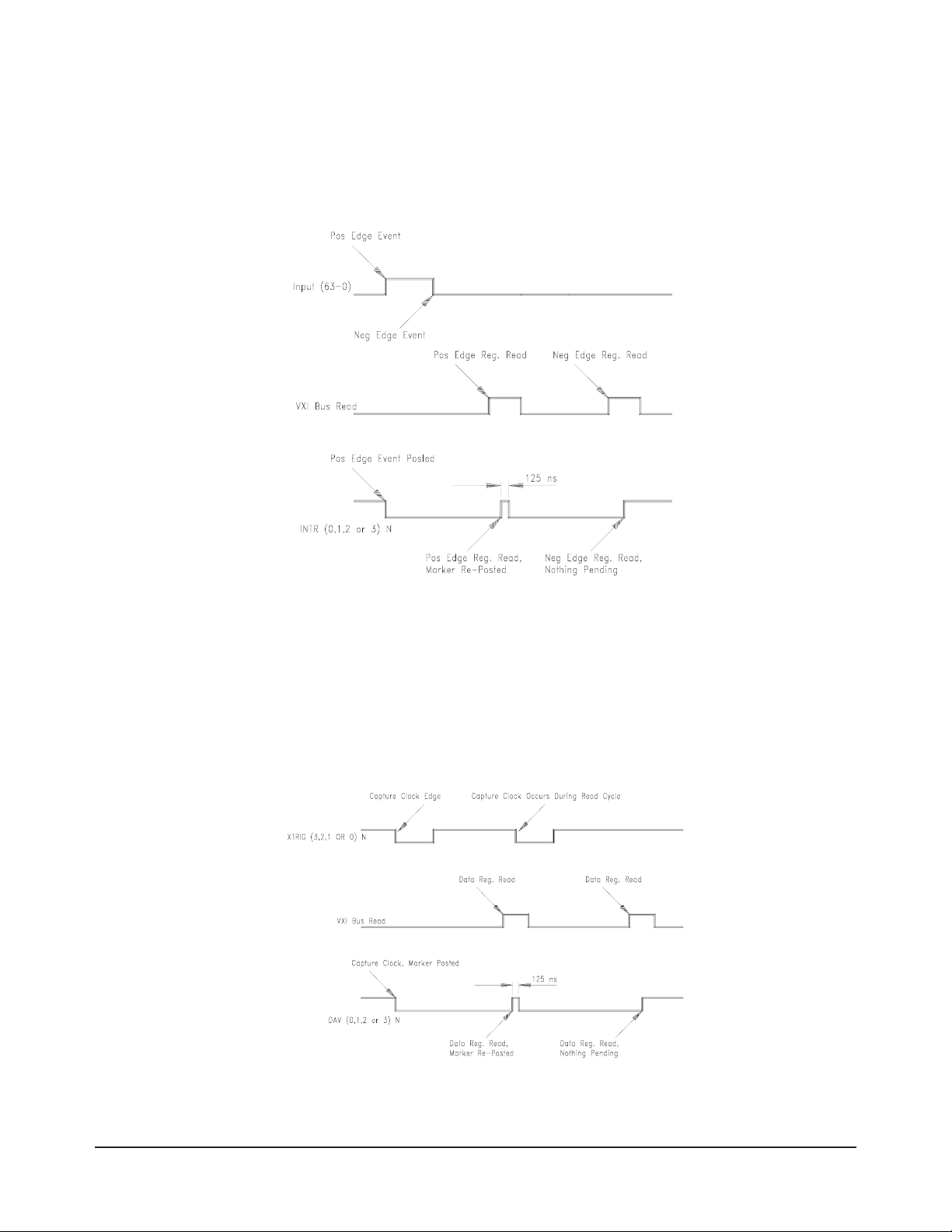
Figure 1-3 demonstrates a typical example. A channel that has been
programmed to detect both positive and negative edge transitions posts a
marker at the occurrence of a positive edge. Before user software can service
this interrupt, a negative transition occurs and is detected. Because both are
detected and the events are marked, user software first reads the positive
edge detect register and then the negative edge detect register.
Figure 1-3. Positive and Negative Edge Transitions
In Figure 1-4, a channel that has been programmed for data capture posts a
marker on the occurrence of an external capture clock. During the
subsequent data register read cycle, another data capture clock occurs to
create a pending DAV (Data AVailable) situation. The second DAV is
retained (and valid) until a subsequent read of the corresponding data
register.
Figure 1-4. DAV Timing
16 Installing and Configuring the HP E1459A
Artisan Technology Group - Quality Instrumentation ... Guaranteed | (888) 88-SOURCE | www.artisantg.com
Page 18

Input Data Capture The state of any channel, within any channel group, may be captured for
subsequent processing (as data) by an externally sourced capture clock
(XTRIG0N - XTRIG3N, the external trigger inputs for each port). Data
channels may be interspersed among all 64 channel inputs, but the user is
cautioned to ensure that all setup criteria and clock sources coincide with
requirements for synchronization. (Each channel group shares a common
capture clock which may not necessarily be synchronous with an external
capture clock of some other channel group.)
If enabled, each register FPGA will post a "Data Available Marker" to the
control FPGA on the occurrence of a corresponding capture clock. Data
Available Markers are cleared by a read of the corresponding "Channel Data
Register." (The static state of these markers may be tested via the "Data
Available Register.") Capture clocks which occur concurrently with a
"register read/marker clear" cycle, are queued and post- processed on
completion of the present cycle. In that event, the marker bit is forced
inactive for a two clock (16 MHz) period before again being posted to the
control FPGA.
In the "Data Capture Mode", the HP E1459A may be programmed to
generate an interrupt on the occurrence of an external capture clock, or an
internal 1.0 MHz sample clock may be selected to allow the state of the data
channels to be tested in the absence of a capture clock. Capture clock
selection (internal/external) is controlled by bit 1 of the Command Register
Word.
Caution A potential hazard exists if software were to improperly
program the HP E1459A to post data-capture IRQ's with the
internally selected 1.0 MHz clock source. I n this situation, a
DAV interrupt would be posted each microsecond (if software
were able to service at that rat e), and would cause software to
continuously vector to interrupt service upon each "return from
service." Therefore, the HP E1459A should never be
programmed to generate DAV interrupts with the internal clock
source selected.
In the HP E1459A the Data Ready Marker is guaranteed to be
cleared when the clock source is switched from internal to
external. Therefore, any capture clock which occurs within the
internal/external clock selection interval will not post a marker
to the control FPGA and will be lost.
Installing and Configuring the HP E1459A 17
Artisan Technology Group - Quality Instrumentation ... Guaranteed | (888) 88-SOURCE | www.artisantg.com
Page 19

Front Panel Markers All "Data Available" and "Edge Detect" marker bits are physicall y available
via the HP E1459A front panel. These outputs are TTL/HC compatible and
may be used to trigger other system-wide events or to provide logging
information for statistical tracking or other performance analysis purposes.
Interrupt Driven or
Polled Mode
Interrupts may be programmatically disabled for both edge-detect and
data-capture events. All registers remain active and valid and may be
serviced on a polled mode basis.
Operations
Interrupt Parsing Since the command module interrupt handler must service multiple,
concurrently-occurring interrupts, (including those which may be sharing
the same IRQ line), some method is necessary to ensure that only a single
IRQ is posted by the HP E1459A during each service interval.
Individual interrupts must be serviced by a commander on a one-for-one
basis. The HP E1459A accomplishes this by inhibiting the generation of a
second IRQ each time an IRQ is posted. THE INHIBIT CONDITION IS
CLEARED BY THE REMOVAL AND REASSERTION OF EITHER
INTERRUPT ENABLE BIT, "DAV" OR "EDGE DETECT." (Refer to
Figure 1-2.)
For this one-for-one interrupt parsing, the HP E1459A REQUIRES that a
global interrupt enable, either DAV or Edge Detect, be disabled and
reasserted within the context of the interrupt service procedure. Normally,
you would simply shut off interrupts at the top of the service procedure, and
would then re-enable them before returning from service. This is the
suggested usage, although this specific sequence is not necessary for proper
HP E1459A hardware function.
18 Installing and Configuring the HP E1459A
Artisan Technology Group - Quality Instrumentation ... Guaranteed | (888) 88-SOURCE | www.artisantg.com
Page 20

Configuring for Installation
Before installing the module you should verify that the following jumpers
and switches are set correctly.
•Logical Address dip switch
•Interrupt priority jumper positions
•Input threshold levels
•Reset time of the Watchdog Tim e r
WARNING SHOCK HAZARD. Only qualified, service-trained personnel who
are aware of the hazards involved should install, configure, or
remove the module. Disconnect all power sources from the
mainframe, the terminal module and installed modules before
installing or removing a module.
WARNING SHOCK HAZARD. When handling user wiring connected to the
terminal module, consider the highest voltage present
accessible on any terminal.
WARNING SHOCK HAZARD. Use wire with an insulation rating greater
than the highest voltage which will be present on the terminal
module. Do not touch any circuit element connected to the
terminal module if any other connector to the terminal module
is energized to more than 30 Vac RMS or 60 Vdc.
Caution MAXIMUM VOLTAGE. Maximum allowable voltage per channel
for this module is 60 Vdc. Up to 115 Vdc or 11 5 Vac RMS can be
applied from one channel to another or from any channel to
chassis.
Caution STATIC-SENSITIVE DEVICE. Use anti-static procedures when
removing, configuring, and installing a module. The module is
susceptible to static discharges. Do not install the module
without its metal shield attached.
Installing and Configuring the HP E1459A 19
Artisan Technology Group - Quality Instrumentation ... Guaranteed | (888) 88-SOURCE | www.artisantg.com
Page 21
Setting the Logical
Address
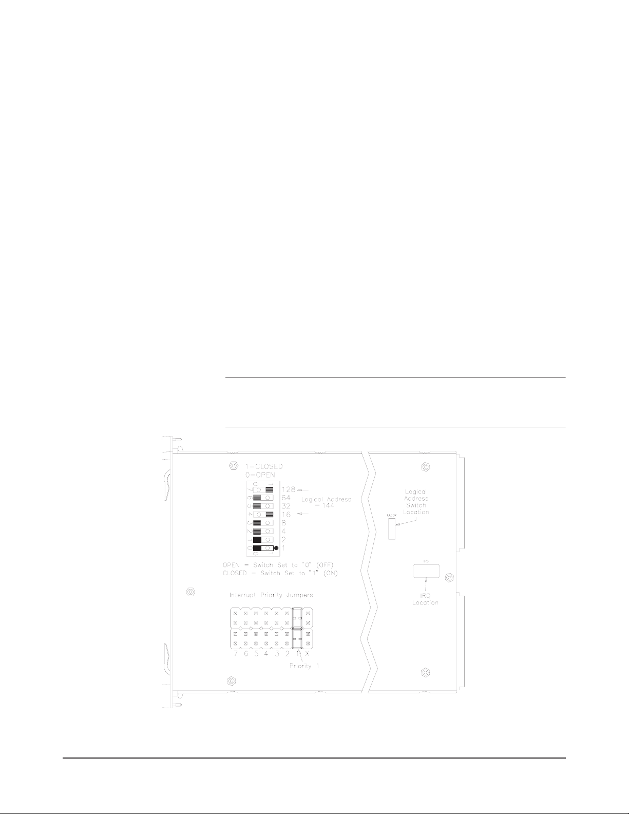
Each module within the VXIbus mainframe must be set to a unique logical
address. The setting is contr olle d by an 8 pin dip switch. This allows for
values from 0 to 255. The factory setting of this switch is decimal 144. No
two modules in the same mainframe can have the same logical address. The
location is shown in Figure 1-5.
Setting the Interrupt
Priority
Note Consult your mainframe manual to be sure that backplane jumpers are
At power on, after a SYSRESET, or after resetting the module via the
control register, all masks will be cleared, interrupts will be disabled, and
internal triggering will be enabled. With interrupts enabled, an interrupt will
be generated whenever an edge occurs on a channel that has been enabled
properly.
The interrupt priority jumper selects which priority level will be asserted.
As shipped from the factory, the interrupt priority jumper should be in
position 1. In most applications this should not be changed. When set to
level X interrupts are disabled. The interrupt priority jumpers are identified
on the sheet metal shield. A hole has been cut into the shield for access to
the jumpers. Interrupts can also be disabled using the Control Register.
The jumper locations ar e shown in Fi gure 1-5. T o change the s ettin g, move
the jumper or jumpers to the desired setting. If the card uses two 2-pin
jumpers versus a single 4 pin jumper, the jumpers must all be placed in the
same row for proper operation.
configured correctly. If you are using the HP E1401B Mainframe these
jumpers are automatically set when the card is installed.
Figure 1-5. HP E1459A Logical Address Switch and IRQ Jumper Locations
20 Installing and Configuring the HP E1459A
Artisan Technology Group - Quality Instrumentation ... Guaranteed | (888) 88-SOURCE | www.artisantg.com
Page 22
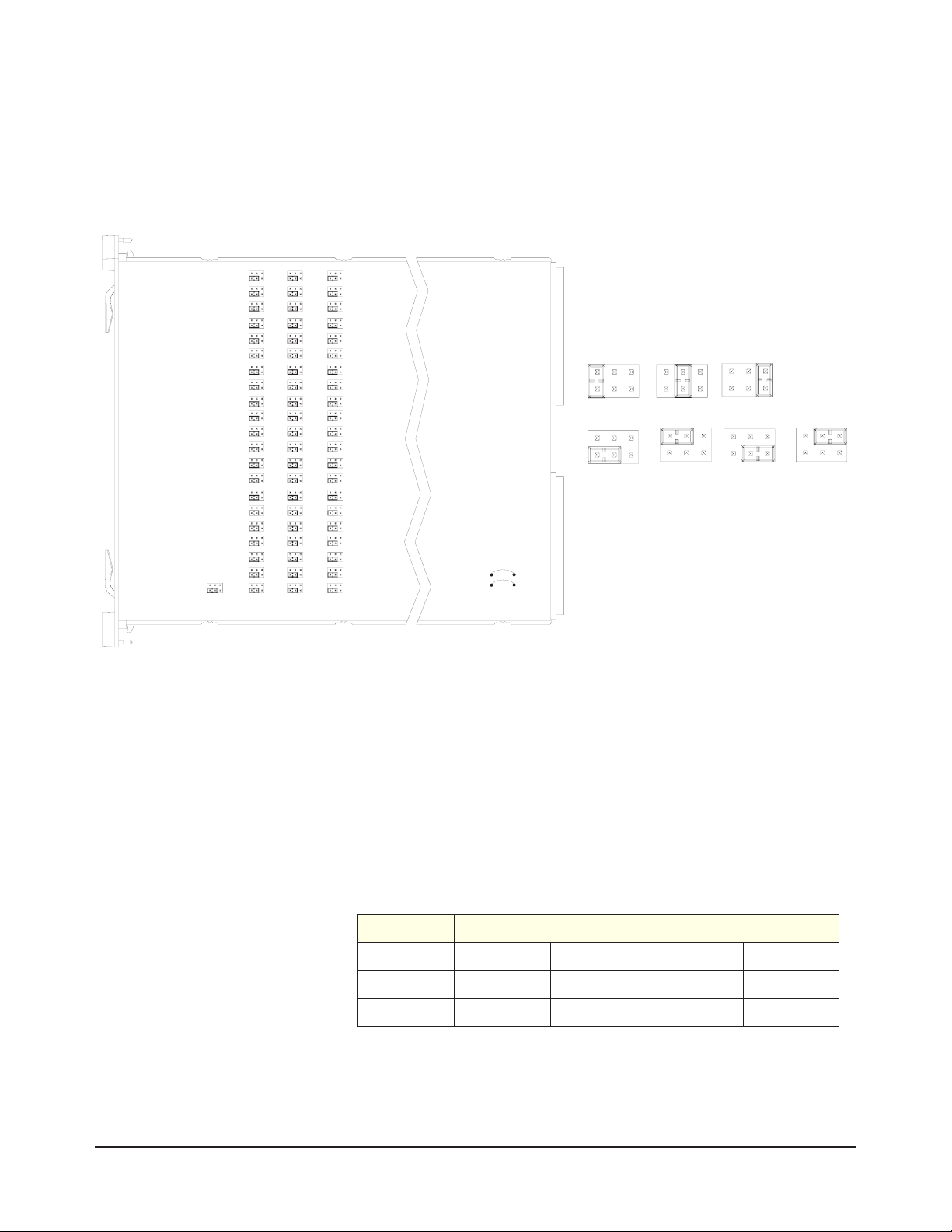
Setting Input
Threshold Levels
1
Ch 0 Ch 2
Ch 3
Ch 6
Ch
The threshold levels for each channel can be set independently. A six pin
plug with a two pin shorting jack is provided for each channel. The channel
can be identified from the silk-screen on the board. Each jumper is labeled
JXCC, where J indicates jumper, X is a number that can be ignored and CC
indicates channel number. The default factory setting is for 5 volts. Pin 1 can
be identified by the square pad on the bottom of the board.
Ch 5
Ch 8
Ch 57 Ch 59
Ch 63
Ch 60
.
Figure 1-6. Input Threshold Level Jumpers and Watchdog Reset Time Jumpers
Setting the Reset
Time on the
Wa tchdog Time r
Ch 61
48 Volt
Ch 62
JM202
JM203
PET Tim e
Jumpers
12 Volt
24 Volt
5 Volt Settings
(Factory Defa ult)
There are 2 jumpers located on the PC board used to control the reset time
of the Watchdog Timer (see Figure 1-6). The reset time is the maximum
allowed time between accesses to keep the Watchdog from asserting
SYSRESET. The Watchdog timer is reset by reading the Watchdog
Control/Status register; use the DIAG:SYSR:STAT? command (see Chapter
3).
.
The following table shows the effect of the jumpers on the reset time. An X
means that the jumper is in place and O indicates the jumper is removed. The
factory default setting is 1.2 second.
Jumper Reset Time
600 ms 150 ms 1.2 sec Not Allowed
JM202 O X O X
JM203 O O X X
Installing and Configuring the HP E1459A 21
Artisan Technology Group - Quality Instrumentation ... Guaranteed | (888) 88-SOURCE | www.artisantg.com
Page 23

Connecting User
Inputs
Port Channels External Trigger Data Available Interrupt
The HP E1459A Isolated Digital Input/Interrupt module consists of a
component module and a terminal block. User inputs for each channel
consists of a low and a high connection for each channel. The inputs will
only detect signals of a positive polarity. A logical "1" will onl y be detected
if the high terminal is at a higher potential than the low terminal. It must also
meet the drive requirements for the voltage threshold selected.
For each block of 16 channels an additional active low input and two active
low outputs are available. The table below lists the signal names and the
associated channels.
0 0 through 15 XTRIG0N DAV0N INTR0N
1 16 through 31 XTRIG1N DAV1N INTR1N
2 32 through 47 XTRIG2N DAV2N INTR2N
3 48 through 63 XTRIG3N DAV3N INTR3N
Figure 1-7 shows the front panel terminals and pinouts for the module. The
cover to the terminal module is silk-screened to indicate the function of each
screw terminal.
22 Installing and Configuring the HP E1459A
Artisan Technology Group - Quality Instrumentation ... Guaranteed | (888) 88-SOURCE | www.artisantg.com
Page 24
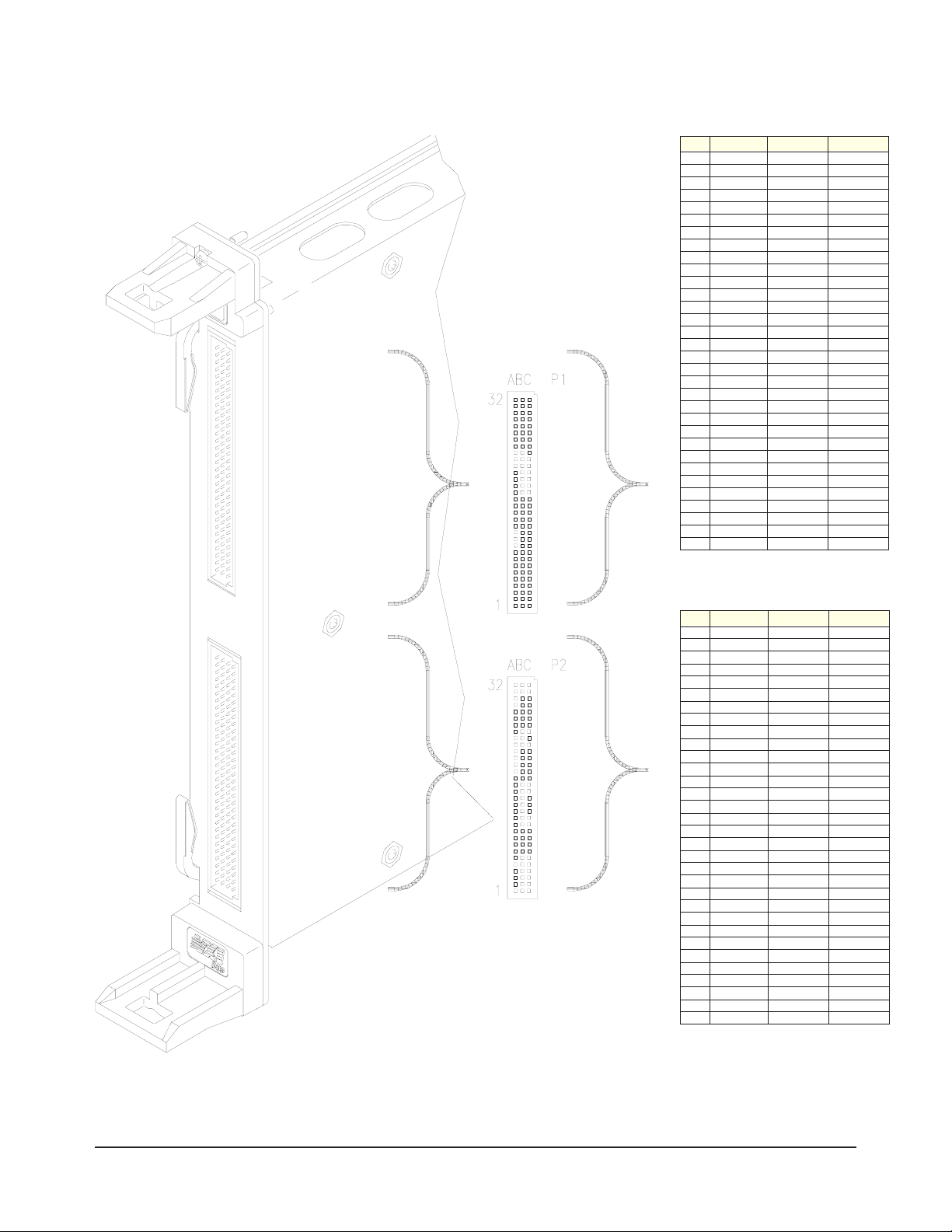
A B C
32 CH 00 HI CH 00 LO
31 CH 01 HI CH 02 LO CH 01 LO
30 CH 02 HI CH 03 LO
29 CH 04 HI CH 03 HI CH 04 LO
28 CH 05 HI CH 05 LO
27 CH 06 HI CH 06 LO
26 CH 07 HI CH 07 LO
25 CH 08 HI CH 08 LO
24 CH 09 HI CH 09 LO
23 CH 10 HI CH 11 LO CH 10 LO
22 CH 11 HI CH 12 LO
21 CH 13 HI CH 12 HI CH 13 LO
20 CH 14 HI CH 14 LO
19 CH 15 HI CH 15 LO
18 CH 16 HI CH 16 LO
17 CH 17 HI CH 17 LO
16 CH 18 HI CH 18 LO
15 CH 19 HI CH 19 LO
14 CH 20 HI CH 20 LO
13 CH 21 HI CH 21 LO
12 CH 22 HI CH 23 LO CH 22 LO
11 CH 23 HI CH 24 LO
10 CH 25 HI CH 24 HI CH 25 LO
9 CH 26 HI CH 26 LO
8 CH 27 HI CH 27 LO
7 CH 28 HI CH 28 LO
6 CH 29 HI CH 29 LO
5 CH 30 HI CH 30 LO
4 CH 31 HI CH 31 LO
3 CH 32 HI CH 32 LO
2 CH 33 HI CH 33 LO
1 CH 34 HI CH 34 LO
A B C
32 CH 35 HI CH 35 LO
31 CH 36 HI CH 37 LO CH 36 LO
30 CH 37 HI CH 38 LO
29 CH 38 HI CH 39 HI CH 39 LO
28 CH 40 HI CH 40 LO
27 CH 41 HI CH 42 LO CH 41 LO
26 CH 42 HI CH 43 LO
25 CH 43 HI CH 44 HI CH 44 LO
24 CH 45 HI CH 45 LO
23 CH 46 HI CH 46 LO
22 CH 47 HI CH 47 LO
21 CH 48 HI CH 48 LO
20 CH 49 HI CH 49 LO
19 CH 50 HI CH 50 LO
18 CH 51 HI CH 51 LO
17 CH 52 HI CH 52 LO
16 CH 53 HI CH 53 LO
15 CH 54 HI CH 55 LO CH 54 LO
14 CH 55 HI CH 56 LO
13 CH 56 HI CH 57 HI CH 57 LO
12 CH 58 HI CH 58 LO
11 CH 59 HI CH 59 LO
10 CH 60 HI CH 61 LO CH 60 LO
9 CH 61 HI CH 62 LO
8 CH 62 HI CH 63 HI CH 63 LO
7
6
5 GND +5VTC GND
4 DAV3N INTR3N XTRIG3N
3 DAV2N INTR2N XTRIG2N
2 DAV1N INTR1N XTRIG1N
1 DAV0N INTR0N XTRIG0N
Figure 1-7. Front Panel Connections
Installing and Configuring the HP E1459A 23
Artisan Technology Group - Quality Instrumentation ... Guaranteed | (888) 88-SOURCE | www.artisantg.com
Page 25
Installing the HP
E1459A in a
VXIbus Mainframe
Set the extraction lev ers out .
1
Extraction
Levers
The HP E1459A may be installed in any C-size VXIbus mainframe slot
(except slot 0). Refer to Figure 1-8 to install the module in a mainframe.
Slide the into any slot
2
(except slot 0) until the backplane
connectors touch.
module
Tighten the top and bottom screws to
4
secure the module to the mainframe .
NOTE: The extraction leverswill not
seat the backplane connectors on older
VXIbus m ainframes. You must manually
seat the connectors by pushingin the
module untilthe module's frontpanel is
flush withthe front of themainframe.
The extraction lev ers m ay be used to
guide or remove the .
To remove the from the mainfram e
reverse the procedure.
module
module
Seat the into the
3
mainframe by pushing in the
extraction levers
,
module
Figure 1-8. Installing the HP E1459A in a VXIbus Mainframe
WARNING To prevent electric shock, tighten faceplate screws when
installing module into mainframe.
24 Installing and Configuring the HP E1459A
Artisan Technology Group - Quality Instrumentation ... Guaranteed | (888) 88-SOURCE | www.artisantg.com
Page 26
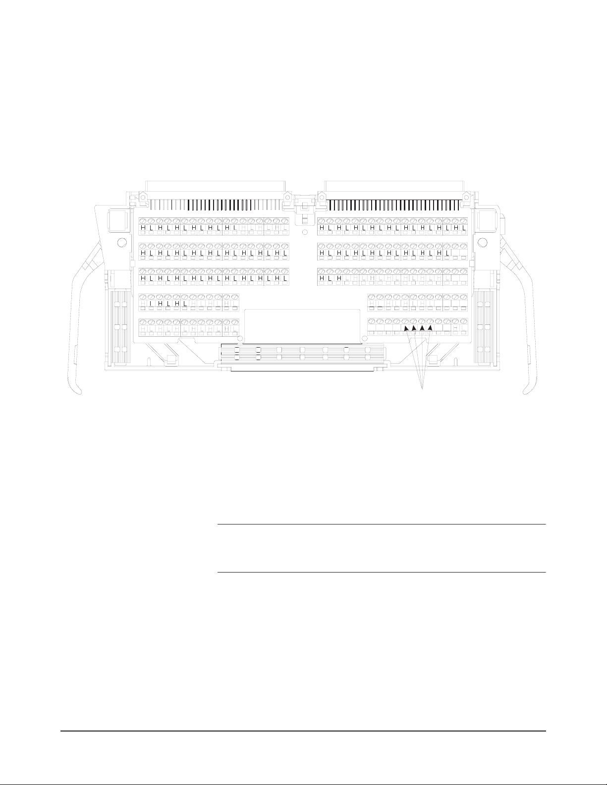
Terminal Block The HP E1459A includes both the input / interrupt module and a screw-t ype
standard terminal block. User inputs to the terminal block are to the High
and Low for each channel, +5Volt, Ground, Data Valid (DAV0 - DAV3),
External Trigger (XTRIG0 - XTRIG3), and Interrupt (INTR0 - INTR3) .
Figure 1-9 shows the HP E1459A’s standard screw-type terminal block
connectors and associated channel numbers. Use the guidelines below to
wire conn ections.
CH0 CH5
CH1
CH2
CH3
CH4
CH6
CH7
CH8
CH9
CH10
CH11
CH12
CH1 3
CH1 4
CH1 5
CH1 6
CH1 7
CH1 8
CH19
CH20
CH21
CH22
CH23
CH24
CH25
CH26
CH27
CH28
+5 G ND
CH29
CH30
CH31
CH32
CH33
CH34
+5 G ND
+5 G ND
+5 G ND
CH35
CH36
CH37
CH38
CH39
CH40
CH41
CH42
CH43
CH44
CH45
CH46
CH47
CH48
CH49
CH50
CH51
CH52
CH56
CH60
CH63
CH53
CH57
CH61
+5 G ND
CH54
CH58
CH62
+5 G ND
CH55
CH59
GNDDAV INT REXT
NotUsed
GNDDAV INT REXT
GNDDAV INT REXT
Figure 1-9. HP E1459A Standard Screw-type Terminal Block
Wiring Guidelines •Be sure the wires make solid connections in the screw terminals.
•Maximum terminal wire size is No. 16 AWG. When wiring all
channels, a smaller gauge wire (No. 20 or 22 AWG) is recommended.
Wire ends should be stripped 5 to 6 mm (0.2 to 0.25 in.) and tinned to
prevent single strands from shorting to adjacent terminals.
WARNING To prevent the spread of fire in the case of a fault, use
flame-rated field wiring whenever the input voltage will exceed
30Vrms, 42Vpeak, or 60Vdc.
Installing and Configuring the HP E1459A 25
Artisan Technology Group - Quality Instrumentation ... Guaranteed | (888) 88-SOURCE | www.artisantg.com
Page 27
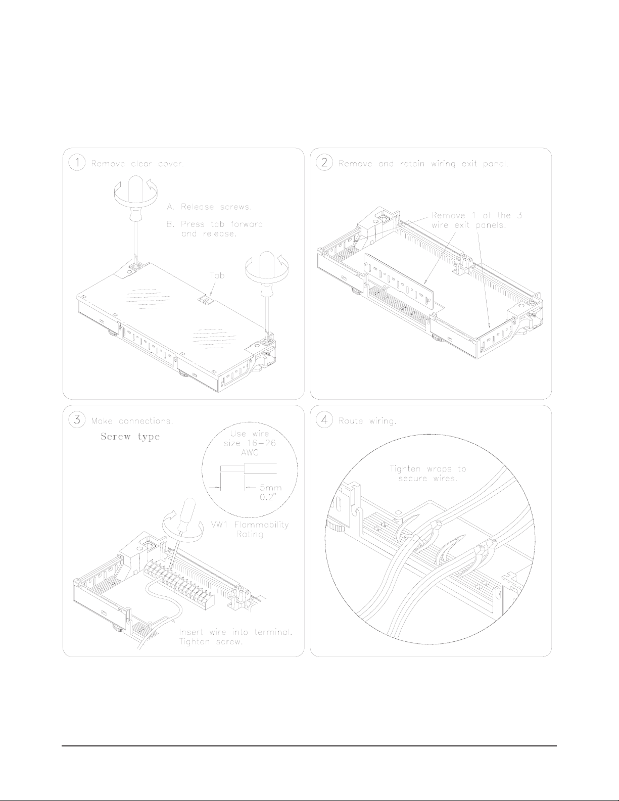
Wiring a Terminal
Block
The following illustrations show how to connect field wiring to the terminal
block.
Continued on Next Page
26 Installing and Configuring the HP E1459A
Artisan Technology Group - Quality Instrumentation ... Guaranteed | (888) 88-SOURCE | www.artisantg.com
Page 28
Replace Wiring Exit Panel
5
Replace Clear Cover
6
A. Hook in the top cover tabs
onto the fixture
B. Press downand
tighten screws
Cut required
holes in panels
for wire exit
Install t he Terminal
7
Module
Keep wiring exitpanel
hole as small as
possible
Push in the E xtractio n Lev ers to Lock the
8
Terminal Module onto the HP E1459A
Extraction
Levers
HP E1459A
Module
Installing and Configuring the HP E1459A 27
Artisan Technology Group - Quality Instrumentation ... Guaranteed | (888) 88-SOURCE | www.artisantg.com
Page 29

28 Installing and Configuring the HP E1459A
Artisan Technology Group - Quality Instrumentation ... Guaranteed | (888) 88-SOURCE | www.artisantg.com
Page 30

Chapter 2
Using the HP E1459A Module
This chapter provides examples of using and programming the HP E1459A
using the Standard Commands for Programmable Instrumentation (SCPI).
For detailed information on all the SCPI commands for this module, refer to
Chapter 3. Appendix B in this manual provides information on registers and
register-based programming.
Note If you are controlling the module by a high level language, such as the
downloaded SCPI driver or the VXIplug&play driver, do not do register
writes. This is because the high level driver will not know the instrument
state and an interrupt may occur causing the driver and/or command
module to fail.
The example programs in this chapter were developed with the ANSI C
language using the HP VISA extensions. For additional information, refer to
the HP VIS A User’s Guide . These programs were written and tested in
Microsoft Visual C++ but should compile under any standard ANSI C
compiler.
To run the programs you must have the HP SICL Library, the HP VISA
extensions, and an HP 82340 or 82341 HP-IB module installed and properly
configured in your PC. An HP E1406 Command Module provides direct
access to the VXI backplane.
Using the HP E1459A Module 29
Artisan Technology Group - Quality Instrumentation ... Guaranteed | (888) 88-SOURCE | www.artisantg.com
Page 31

Power-on / Reset States
At power-on or reset (*RST) the HP E1459A is set to the following
conditions:
•Watchdog timer is off (disabled).
•Clock Source is Internal
•Input Debounce Time is 18.0 µS.
•DAV (Data Available) Event interrupts are disabled for all ports.
•Edge Event interrupts are disabled for all ports.
Example 1:
Reset, Self Test,
and Module ID
Also, refer to the
STATus:PRESet command in Chapter 3.
This first example resets the HP E1459A, performs the module self test, and
reads the module ID and description.
/* Self Test
This program resets the HP E1459A, performs a Self Test,
and reads the ID string
Created in Microsoft Visual C++ */
#include <visa.h>
#include <stdio.h>
#include <stdlib.h>
#define INSTR_ADDR "GPIB0::9::3::INSTR"
int main()
{
ViStatus errStatus;
ViSession viRM;
ViSession E1459;
char id_string [256] = {0};
char selftst_string[256] = {0};
/* HP E1459A logical address */
/* status from VISA call */
/* Resource Mgr. session */
/* session for HP E1459A */
/* ID string buffer */
30 Using the HP E1459A Module
Artisan Technology Group - Quality Instrumentation ... Guaranteed | (888) 88-SOURCE | www.artisantg.com
Open a default Resource Manager
/*
errStatus = viOpenDefaultRM (&viRM);
if (VI_SUCCESS > errStatus){
printf("ERROR: viOpen() returned 0x%x\n",errStatus);
return errStatus;}
Open the Instrument Session
/*
errStatus = viOpen (viRM, INSTR_ADDR,VI_NULL ,VI_ NULL , &E14 59);
if (VI_SUCCESS > errStatus){
printf("ERROR: viOpen() returned 0x%x\n",errStatus);
return errStatus;}
Reset the E1459A
/*
errStatus = viPrintf (E1459, "*RST;*CLS\n");
if (VI_SUCCESS > errStatus){
printf("ERROR: viPrintf() returned 0x%x\n",errStatus);
return errStatus;}
*/
*/
*/
Page 32

/*
Send the Self Test Command
*/
errStatus = viQueryf (E1459, "*TST?\n","%t",selftst_string);
if (VI_SUCCESS > errStatus){
printf("ERROR: viQueryf() returned 0x%x\n",errStatus);
return errStatus;}
printf("Self Test Result is %s\n",selftst_string);
Query the ID string
/*
*/
errStatus = viQueryf (E1459, "*IDN?\n","%t",id_string);
if (VI_SUCCESS > errStatus){
printf("ERROR: viQueryf() returned 0x%x\n",errStatus);
return errStatus;}
printf("IDN? returned %s\n",id_string);
Close Sessions
/*
*/
errStatus = viClose (E1459);
if (VI_SUCCESS > errStatus){
printf("ERROR: viClose() returned 0x%x\n",errStatus);
return 0;}
errStatusviClose (viRM);
if (VI_SUCCESS > errStatus){
printf("ERROR: viClose() returned 0x%x\n",errStatus);
return 0;}
}
/* End of main program */
Using the HP E1459A Module 31
Artisan Technology Group - Quality Instrumentation ... Guaranteed | (888) 88-SOURCE | www.artisantg.com
Page 33

Digital Input The HP E1459A is capable of simple digital inputs on any of the individual
four ports or combined Ports 0 and 1 or Ports 2 and 3. The
command subsystem (see Chapter 3 for details) provides two commands for
reading the current value of the input ports:
MEASure
Example 2:
Digital Input
MEASure:DIGital:DATAn:
MEASure:DIGital:DATAn :
type
:VALue? — reads the current port value
type
:BITm? — reads an individual bit value
This program reads Port 0 as an individual 16-bit port and then it reads the
combined Ports 2 and 3 as a 32-bit port. The values returned are a signed
16-bit integer for Port 0 and a signed 32-bit integer for combined Ports 2 and
3. Although this program does not decode the returned value to determine
individual bit/channel values, a "0" in any bit position indicates the input to
the corresponding channel is low; a "1" in any bit position indicates the
input to the corresponding channel is high.
/* Digital Input Example
This program reads the current value of Port 0 (16-bit word)
and combined value of Ports 2 and 3 (32-bit word)
Created in Microsoft Visual C++ */
#include <visa.h>
#include <stdio.h>
#include <stdlib.h>
#define INSTR_ADDR "GPIB0::9::3::INSTR"
int main()
{
ViStatus errStatus;
ViSession viRM;
ViSession E1459;
int val;
long va l1;
/* HP E1459A logical address */
/* status from VISA call */
/* Resource Mgr. session */
/* session for HP E1459A */
/* value of Port 0 */
/*Value of Ports 2 & 3 */
32 Using the HP E1459A Module
Artisan Technology Group - Quality Instrumentation ... Guaranteed | (888) 88-SOURCE | www.artisantg.com
Open a default Resource Manager
/*
errStatus = viOpenDefaultRM (&viRM);
if (VI_SUCCESS > errStatus){
printf("ERROR: viOpen() returned 0x%x\n",errStatus);
return errStatus;}
Open the Instrument Session
/*
errStatus = viOpen (viRM, INSTR_ADDR,VI_NULL ,VI_ NULL , &E14 59);
if (VI_SUCCESS > errStatus){
printf("ERROR: viOpen() returned 0x%x\n",errStatus);
return errStatus;}
Query Port 0 as a 16-bit word
/*
errStatus = viQueryf(E1459, "MEAS:DIG:DATA0:WORD:VAL?\n","%t", val);
if (VI_SUCCESS > errStatus){
printf("ERROR: viQueryf() returned 0x%x\n",errStatus);
return errStatus;}
printf("Value returned %i\n",val);
*/
*/
*/
Page 34

/*
Query Ports 2 and 3 as a 32-bit word
*/
errStatus = viQueryf(E1459, "MEAS:DIG:DATA2:LWORD:VAL?\n"," %t" , va l1);
if (VI_SUCCESS > errStatus){
printf("ERROR: viQueryf() returned 0x%x\n",errStatus);
return errStatus;}
printf("Value returned %i\n",val1);
Close Sessions
/*
*/
errStatus = viClose (E1459);
if (VI_SUCCESS > errStatus){
printf("ERROR: viClose() returned 0x%x\n",errStatus);
return 0;}
errStatus = viClose (viRM);
if (VI_SUCCESS > errStatus){
printf("ERROR: viClose() returned 0x%x\n",errStatus);
return 0;}
}
/* End of main program */
Using the HP E1459A Module 33
Artisan Technology Group - Quality Instrumentation ... Guaranteed | (888) 88-SOURCE | www.artisantg.com
Page 35

Edge Detected Event Detection
The HP E1459A can respond to two types of events: Edge Events (either
negative edge, positive edge, or both) and Data Available. Figures 2-1 and
2-2 show the general flow of commands necessary to program the HP
E1459A to detect events. Figure 2-1 shows the flow for Edge Event
Detection, Figure 2-2 shows the flow for Data Available Event Detection.
Three general methods of identifying and servicing an HP E1459A detected
event are:
•Polling the Port Summary Register
•Polling the VXI Status Subsystem
•SRQ Interrupt
When an Edge Event occurs, read the value of the port(s) with the
[SENSe:]EVENt:PORTn:NEDGe? or [SENSe:]EVENt:PORTn:PEDGe?
command. When a Data Available Event occurs, read the value of the port(s)
with the
MEASure:DIGital:DATAn command.
Polling the Port
Summary Register
Polling the Status
Subsystem
The first, and easiest method, is to repeatedly poll the Port Summary
Register using either the
Edge Events) or the
Data Available Events) until an event occurs. Example 3 in this chapter
demonstrates this procedure.
The second method is to set-up and repeatedly poll the Status Subsystem.
You can poll the port summary condition register with the
STATus:OPERation:PSUMmary:CONDition? command to determine when
an event has occurred.
Alterna tely, set-up the port summary enable register to specify the type of
event(s) and port(s) to monitor; use the
STATus:OPERation:PSUMmary:ENABle<
bit 9 in the Status Operation Enable register; use the
STATus:OPERation:ENABle command. Repeatedly poll the module with
STB? command to determine when bit 7 becomes set.
the *
SENSe:EVENt:PSUMmary:EDGE? command (for
SENSe:EVENt:PSUMmary:DAVailable? command (for
mask
> command. Then enable
SRQ Interrupt The third method is to set-up the Stat us Subsystem and have th e HP E1459A
Module interrupt (via SRQ) the system computer when an event occurs. In
general, you must set-up the port summary enable register to specif y the type
of event(s) and port(s) to monitor; use the
STATus:OPERation:PSUMmary:ENABle<
bit 9 in the Status Operation Enable register; use the
STATus:OPERation:ENABle command. Enable the OPR bit (bit 7) in the
Status Register with the
Status register to generate the SRQ.
*SRE 128 command; this allows the Operation
mask
> command. Then, enable
34 Using the HP E1459A Module
Artisan Technology Group - Quality Instrumentation ... Guaranteed | (888) 88-SOURCE | www.artisantg.com
Page 36

HP E1459A Edge Event Detection Flowchart
Unmask all 16 bits of Port.
(Either Positive, Negative,
or both.)
Optionally, set the
Debounce Time
Enable the Edge Detection
[SENSe:]EVENt:PORTn:NEDGE:ENABle <
[SENSe:]EVENt:PORT
INPut
n
:DEBounce:TIMe <
[SENSe:]EVENt:PORT
n
:PEDGE:ENABle <
time
>
n
:EDGE:ENABle <
mask
mask
state
>
>
>
Wait for the Event to Occur.
Do one of the following:
1. Poll the Port Summary Register
2. Poll the Status Subsystem
3. Use SRQ to interrupt
Read the data and clear the
event detector register
Figure 2-1. HP E1459A Edge Event Detection Flowchart
[SENSe:]EVENt:PSUMmary:EDGe?
STATus:OPERation:PSUMmary:CONDition?
STATus:OPERation:PSUMmary:ENABle <
STATus:OPERation:ENABle 512
*SRE128
[SENSe:]EVENt:PORTn:NEDGe?
[SENSe:]EVENt:PORT
n
:PEDGe?
mask
>
Using the HP E1459A Module 35
Artisan Technology Group - Quality Instrumentation ... Guaranteed | (888) 88-SOURCE | www.artisantg.com
Page 37

HP E1459A Data Available Event Detection Flowchart
Set External Clock Source
Optionally, set the
Debounce Time
Enable the DAV Detection
INPutn:CLOCk[:SOURce]EXT
INPutn:DEBounce:TIMe <
[SENSe:]EVENt:PORT
n
:DAVailable:ENABle <
time
>
state
>
Wait for the Event to Occur.
Do one of the following:
1. Poll the Port Summary Register
2. Poll the Status Subsystem
3. Use SRQ to interrupt
Read the data and clear the
event detector register
Figure 2-2. HP E1459A Data Available Event Detection Flowchart
[SENSe:]EVENt:PSUMmary:DAV?
STATus:OPERation:PSUMmary:CONDition?
STATus:OPERation:PSUMmary:ENABle <
STATus:OPERation:ENABle 512
*SRE128
MEASure:DIGital:DATAn:
MEASure:DIGital:DATA
type
n:type
:VALue?
:BITm?
mask
>
36 Using the HP E1459A Module
Artisan Technology Group - Quality Instrumentation ... Guaranteed | (888) 88-SOURCE | www.artisantg.com
Page 38

Example 3:
Edge Interrupt
This example repeatedly polls the Port 0 Port Summary Edge Detection
Register to determine when an edge event occurs. When an event occurs, the
program reads the values of the Positive and Negative Edge Registers and
returns the values. The values returned are in the range of -32768 to +32767.
Although this program does not decode this returned value to determine
individual bit/channel values, a "0" in any bit position indicates an edge
event was not
detected for the corresponding channel; a "1" in any bit
position indicates an edge event was detected for the corresponding channel.
/* Edge Interrupt Example
This program sets both positive and negative edge detection,
queries the Port Summary Edge Detection Register in a loop
until an event occurs. The program then read the PEDGE and NEDGE
registers and returns the current value.
Created in Microsoft Visual C++ */
#include <visa.h>
#include <stdio.h>
#include <stdlib.h>
#define INSTR_ADDR "GPIB0::9::3::INSTR"
int main()
{
ViStatus errStatus;
ViSession viRM;
ViSession E1459;
int val, event;
Open a default Resource Manager
/*
errStatus = viOpenDefaultRM (&viRM);
if (VI_SUCCESS > errStatus){
printf("ERROR: viOpen() returned 0x%x\n",errStatus);
return errStatus;}
Open the Instrument Session
/*
errStatus = viOpen (viRM, INSTR_ADDR,VI_NULL ,VI_ NULL , &E14 59);
if (VI_SUCCESS > errStatus){
printf("ERROR: viOpen() returned 0x%x\n",errStatus);
return errStatus;}
Unmask the negative edge events for Port 0
/*
errStatus = viPrintf (E1459, "EVEN:PORT0:NEDG:ENAB 0xFFFF\n");
if (VI_SUCCESS > errStatus){
printf("ERROR: viPrintf() returned 0x%x\n",errStatus);
return errStatus;}
*/
*/
/* HP E1459A logical address */
/* status from VISA call */
/* Resource Mgr. session */
/* session for HP E1459A */
*/
Unmask the positive edge events for Port 0
/*
errStatus = viPrintf (E1459, "EVEN:PORT0:PEDG:ENAB 0xFFFF\n");
if (VI_SUCCESS > errStatus){
printf("ERROR: viPrintf() returned 0x%x\n",errStatus);
return errStatus;}
Set Port 0 debounce time to 1.13 mS
/*
errStatus = viPrintf (E1459, "INP0:DEB:TIM 1E-3\n");
Using the HP E1459A Module 37
Artisan Technology Group - Quality Instrumentation ... Guaranteed | (888) 88-SOURCE | www.artisantg.com
*/
*/
Page 39

if (VI_SUCCESS > errStatus){
printf("ERROR: viPrintf() returned 0x%x\n",errStatus);
return errStatus;}
Enable Port 0 Edge Detection
/*
*/
errStatus = viPrintf (E1459, "EVEN:PORT0:EDGE:ENAB ON\n");
if (VI_SUCCESS > errStatus){
printf("ERROR: viPrintf() returned 0x%x\n",errStatus);
return errStatus;}
Loop and poll Port Summary Register until event occurs
/*
*/
while (event = 0)
{
errStatus = viQueryf (E1459, "EVEN:PSUM:EDGE?\n","%t",event);
if (VI_SUCCESS > errStatus){
printf("ERROR: viPrintf() returned 0x%x\n",errStatus);
return errStatus;}
}
Read NEDGE register and clear event detector register
/*
*/
errStatus = viQueryf (E1459, "EVEN:PORT0:NEDGE?\n","%t",val);
if (VI_SUCCESS > errStatus){
printf("ERROR: viPrintf() returned 0x%x\n",errStatus);
return errStatus;}
printf ("Negative Edge Event value = %s\n",val);
Read PEDGE register and clear event detector register
/*
*/
errStatus = viQueryf (E1459, "EVEN:PORT0:PEDGE?\n","%t",val);
if (VI_SUCCESS > errStatus){
printf("ERROR: viPrintf() returned 0x%x\n",errStatus);
return errStatus;}
printf ("Positive Edge Event value = %s\n",val);
Close Sessions
/*
*/
errStatus = viClose (E1459);
if (VI_SUCCESS > errStatus){
printf("ERROR: viClose() returned 0x%x\n",errStatus);
return 0;}
errStatus = viClose (viRM);
if (VI_SUCCESS > errStatus){
printf("ERROR: viClose() returned 0x%x\n",errStatus);
return 0;}
}
/* End of main program */
38 Using the HP E1459A Module
Artisan Technology Group - Quality Instrumentation ... Guaranteed | (888) 88-SOURCE | www.artisantg.com
Page 40

HP E1459A SCPI Command Reference
The Standard Commands for Programmable Instruments (SCPI) commands
described in this chapter are only available in the downloadable SCPI driver for the
HP Command Modules such as the HP E1406. If you are not using a command
module, you shou ld use the HP VXIplug&play driver. This driver is available on the
HP Instrument Drivers CD and available on the World Wide Web.
Common Command Format
The IEEE 488.2 standard defines the Common commands that perform functions
like reset, self-test, status byte query, etc. Common commands are four or five
characters in length, always begin with the asterisk character (*), and may include
one or more parameters. The command keyword is separated from the first
parameter by a space character. Some examples of common commands are shown
below:
*RST *ESR 32 *STB?
Chapter 3
SCPI Command Format
The SCPI commands perform functions such as making measurements, querying
instrument states, or retrieving data. A command subsystem structure is a
hierarchical structure that usually consists of a top level (or root) command, one or
more low-level commands, and their parameters. The following example shows the
root command DISPlay and some of its lower-level subsystem commands:
Command
Separator
:DISPlay
:DISPlay is the root command, :MONitor is a second level commands, and :PORT,
PORT?, [:STATe], and [:STATe]? are third level commands.
A colon (:) always separates one command from the next lower level command:
DISPlay:MONitor:PORT <
Colons separate the root command from the second level command
DISPlay:MONitor) and the second level from the third level (MONitor:CHANnel).
(
:MONitor
:PORT <port>
:PORT? [MINimum | MAXimum | DEFault]
[:STATe] <state>
[:STATe]?
port
>.
Abbreviated
Commands
Artisan Technology Group - Quality Instrumentation ... Guaranteed | (888) 88-SOURCE | www.artisantg.com
The command syntax shows most commands as a mixture of upper and lower case
letters. The upper case letters indicate the abbreviated spelling for the command. For
shorter program lines, send the abbreviated form. For better program readability, you
may send the entire command. The instrument will accept either the abbreviated
form or the entire command.
HP E1459A SCPI Command Reference 39
Page 41

For example, if the command syntax shows DISPlay, then DISP and DISPLAY are
both acceptable forms. Other forms of
an error. You may use upper or lower case letters. Therefore,
DiSpLaY are all acceptable.
DISPlay, such as DISPL or DISPl will generate
DISPLAY, display, and
Implied
Commands
Command
Parameters
Implied commands are those which appear in square brackets ([ ]) in the command
syntax. (Note that the brackets are not part of the command and are not sent to the
instrument.) Suppose you send a command but do not send the associated implied
command. In this case, the instrument assumes you intend to use the implied
command and it responds as if you had sent it. For example:
DISPlay:MONitor[:STATe] <state>
The third level command [:STATe] is an implied command. For example, to set the
display monitor state, you can send either of the following command statements:
DISPlay:MONitor <state> or DISPlay:MONitor:STATe <state>
Parameter Types . The following table contains explanations and examples of
parameter types you might see later in this chapter.
Parameter Type Explanations and Example
Numeric Accepts all commonly used decimal representations of number including
optional signs, decimal points, and scientific notation.
123, 123E2, -123, -1.23E2, 0.123, 1.23E-2, 1.23000E-01.
Special cases include MINimum, MAXimum, and DEFault.
Boolean Represents a single binary condition that is either true or false.
Linking
Commands
ON, OFF, 1, 0
Discrete Selects from a finite number of values. These parameters use mnemonics to
represent each valid setting.
An example is the TRIGger:SOURce <source>
command where source can be BUS, EXT, or IMM.
Optional Parameters. Parameters shown within square brackets ([ ]) are optional
parameters. (N o te th a t th e b rackets are not part of th e command and are not sent to
the instrument.) If you do not specify a value for an optional parameter, the
instrument chooses a default value. For example, consider the
:PORT? [MIN | MAX]
command. If you send the command without specifying a MINimum or MAXimum
parameter, the present
command returns the minimum current display channel. If you send the
PORT? value is returned. If you send the MIN parameter, the
MAX
parameter, the command returns the maximum display channel. Be sure to place a
space between the command and the parameter.
Linking IEEE 488.2 Common Commands with SCPI Commands. Use a
semicolon between the commands. For example:
*RST;DISP:MON ON or DISP:MON ON;*TRG
Linking Multiple SCPI Commands. Us e both a semico lon and a colon b etween the
commands. For example:
DISP:MON:PORT 0;:MEAS:DIG:DATA0:WORD::VAL?
40 HP E1459A SCPI Command Reference
Artisan Technology Group - Quality Instrumentation ... Guaranteed | (888) 88-SOURCE | www.artisantg.com
Page 42

DIAGnostic:SYSReset Subsystem
The DIAGnostic:SYSReset Subsystem controls and monitors the Watchdog Timer.
Refer to Chapter 1 for detailed information on the Watchdog Timer.
Syntax DIAGnostic:SYSReset
DIAGnostic:SYSReset[:S TATe]?
Returns the value of the Watchdog Timer state from the Watchdog Timer Control /
Status Register.
Parameters None
Comments • Returns a 1 if the Watchdog Timer is asserted; returns a 0 if the Timer is not
asserted.
•Reading this register resets the Wa tchdog T imer.
•If the Watchdog timer is enabled, the state of the timer MUST be read before
the Watchdog time elapses. If the state is not read before the time elapses, the
Watchdog Timer asserts the VXIbus SYSRESET line.
[:STATe]? page 41
:ENABle <state> page 41
:ENABle? page 42
DIAGnostic:SYSReset:ENABle <
Turns the Watchdog Timer ON o r OFF.
Parameters
Parameter Name Parameter Type Range of Values Default
<
state
> numeric or discrete 0, 1, OFF, ON 0, OFF
Comments • A 0 or OFF turns the Watchdog Timer off; a 1 or ON turns the Timer on.
•CAUTION: When the Watchdog Timer is enabled (ON), the VXIbus
backplane SYSRESET line is asserted if the Watchdog Timer is allowed to
elapse. The Watchdog T imer is reset each time the state of the Timer is read by
the DIAG:SYSR:STAT? command.
Example DIAG:SYSR:ENAB ON
state
>
Turns Watchdog Timer on
HP E1459A SCPI Command Reference 41
Artisan Technology Group - Quality Instrumentation ... Guaranteed | (888) 88-SOURCE | www.artisantg.com
Page 43

DIAGnostic:SYSReset:ENABle?
Returns the state of the Watchdog Timer as either a (unsigned) 1, or 0.
Parameters None
Comments Returns a 1 if the Watchdog Timer is enabled. Returns a 0 if the Timer is not enabled.
42 HP E1459A SCPI Command Reference
Artisan Technology Group - Quality Instrumentation ... Guaranteed | (888) 88-SOURCE | www.artisantg.com
Page 44

DISPlay:MONitor Subsystem
The DISPlay:MONitor subsystem turns on the monitor mode. Parameters related to
the state of the data and control lines are shown on an external terminal
Command Module’s Users’s Guide for supported terminal types. The
DISPlay:MONitor commands do not apply to any C-SCPI or VXIplug&play driver
implementation. The parameters displayed are:
Syntax DISPlay:MONitor
DISPlay:MONitor:POR T <
Sets the value of the DISPlay:MONitor:PORT or sets the automatic display mode.
Parameters
Parameter Name Parameter Type Range of Values Default
<
port
> numeric or discrete 0, 1, 2, 3, AUTO, MINimum, MAXimum,
:PORT <
:PORT? [MINimum | MAXimum | DEFault] page 44
:PORT:AUTO <state> page 44
:PORT:AUTO? page 44
[:STATe] <
[:STATe]? page 4 5
port
>
port
> page 43
state
> page 4 5
DEFault
1
. Refer to the
AUTO
Comments • Sets the value of the Display Monitor to Port 0, 1, 2, or 3. AUTO automatically
displays the results of a MEAS:DIG:DATAn? command whenever that
command is executed for the monitored Port if the display monitor is active for
the Port. MINimum or DEFault sets the value for the monitored Port to 0.
MAXimum sets the value for the monitored Port to 3.
•Specifying either 0, 1, 2, 3, MIN, MAX, or DEF turns the AUTO mode off.
•*RST Condition: sets the display Port to 0 and the automatic display mode
ON.
Example DISP:MON:PORT2
DISP:MON:PORT AUTO
1.The display monitor is an RS-232 T erminal attached to an HP E1405B, E1406, or E1306 Command Module and
provides an interactive user interface to the HP E1459A.
Display data from port 2
Set automatic display mode
HP E1459A SCPI Command Reference 43
Artisan Technology Group - Quality Instrumentation ... Guaranteed | (888) 88-SOURCE | www.artisantg.com
Page 45

DISPlay:MONitor:PORT? [MINimum | MAXimum | DEFault]
Returns the number of the current display Port as +0, +1, +2, or +3.
Parameters None
Comments • When sent with no parameter, this query returns a decimal number indicating
the Port being monitored. If AUTO was selected as the Port parameter in the
DISP:MON:PORT <port> command, the query returns the number of the most
recently-viewed Port. If either MINimum or DEFault was specified, this quer y
returns a +0. If MAXimum was specified, this query returns a +3.
DISPlay:MONitor:PORT:AUTO <
Sets the automatic mode for the Display Monitor on or off. When AUTO mode is
ON, the port being monitored is automatically set to the last last port measured.
Parameters
Parameter Name Parameter Type Range of Values Default
<state> numeric or discrete 0, 1, OFF, ON OFF
Comments • a 0 or OFF turns the display monitor automatic mode off; a 1 or ON turns the
display monitor automatic mode on.
•*RST Condition: sets the automatic mode on.
Example DISP:MON:PORT:AUTO ON
DISPlay:MONitor:PORT:AUTO?
Returns the state of the automatic display mode as either +0 or +1.
Parameters None.
state
>
Turns automatic display mode on
Comments • A 0 indicates the automatic display mode is OFF; a 1 indicates the automatic
displa y mode is ON.
•*RST Condition: sets the automatic mode on.
44 HP E1459A SCPI Command Reference
Artisan Technology Group - Quality Instrumentation ... Guaranteed | (888) 88-SOURCE | www.artisantg.com
Page 46

DISPlay:MONitor[:STATe] <
Turns the Display Mode on or off.
Parameters
Parameter Name Parameter Type Range of Values Default
<state> Numeric or discrete 0 | 1 | OFF | ON OFF
Comments • DISP:MON ON enables the terminal display of Port parameters. The
parameters are updated to the terminal following each new command
accessing a Port.
•The displayed data is in the format:
-- Displayed port number: 0, 1, 2, or 3
-- Size of the data: 16-bit word or 32-bit word
-- Actual data: signed decimal and hexadecimal
•A keyboard entry at the terminal sets DISP:MON OFF.
•*RST Condition: OFF.
state
>
Example DISP:MON ON
DISPlay:MONitor[:STATe]?
Returns the value of the Display Monitor State as either 0 (for OFF) or 1 (for ON).
Parameters None
Comments • DISP:MON[:STAT]? returns a 1 if the monitor mode is on; or returns a 0 if the
monitor mode is off.
Example DISP:MON?
turns the display mode on.
HP E1459A SCPI Command Reference 45
Artisan Technology Group - Quality Instrumentation ... Guaranteed | (888) 88-SOURCE | www.artisantg.com
Page 47

INPut Subsystem
The INPut Subsystem configures the input de-bounce circuitry and specifies the
input clock source.
Syntax INPut
n
:CLOCk[:SOURce] <
:CLOCk[:SOURce]? page 47
:DEBounce:TIME <
:DEBounce:TIME? [MINimum | MAXimum | DEFault] page 48
INPutn:CLOCk[:SOURce] <
Specifies the input circuitry clock source for Port n.
Parameters
Parameter Name Parameter Type Range of Values Default
INPut
n
<
source
>
Comments • When the clock source is set to INTernal, the input data is sampled by the
internal clock. When the clock is set to EXTernal, the input data is sampled on
negative-edge transitions of the input clock.
•This is the clock source for clocking new data from the optical isolators into
the input circuitry. New data is automatically clocked into the input debounce
circuitry for each clock pulse of the internal clock when the clock source is
INTernal. Refer to the INPut:DEBounce:TIME command to set the Debounce
time.
• For a clock source of EXTernal, new data is clocked into the input circuitry
when the external clock receives a clock pulse. Data is clocked into the input
circuitry on the positive edge of the external clock.
•Note that the debounce circuitry, current value registers, and event detectors
are always clocked by the internal clock.
•Note: if a Data Available Event is enabled for the port, attempting to set the
clock source to INTernal will result in an error -221, "Settings Conflict".
•*RST Condition: sets the input clock source to INTernal.
source
numeric
discrete
>
source
time
> page 46
> | MINimum | MAXimum | DEFault page 47
0, 1, 2, 3
INTernal, EXTernal
0
INT
Example INP1:CLOC:SOUR EXT
46 HP E1459A SCPI Command Reference
Artisan Technology Group - Quality Instrumentation ... Guaranteed | (888) 88-SOURCE | www.artisantg.com
Sets the input clock source for Port 1 to
External
Page 48

INPutn:CLOCk[:SOURce]?
Returns the programmed value of the input clock source for Port n.
Parameters
Parameter Name Parameter Type Range of Values Default
INPut
n
Comments • The value returned is an unquoted string of EXT or INT.
numeric 0, 1, 2, 3 0
Example INPut2:CLOCk[:SOURce]?
INPutn:DEBounce:TIME <
Programs the input debounce time for Port n. Ports 0 and 1 share the same debounce
circuitry; Ports 2 and 3 share the same debounce circuitry.
Parameters
Parameter Name Parameter Type Range of Values Default
INPut
n
<time>
DEFault
MINimum
MAXimum
Comments • The available debounce times are:
18.0 µS, 36 µS, 72 µS, 144 µS, 288 µS, 576 µS, 1.13 mS , 2.26 mS, 4.6 mS, 9.2
mS, 18.4 mS, 36.9 mS, 73.8 mS, 148.0 mS, 294.0 mS, 590.0 mS, 1.18 S, 2.36
S, 4.72 S, 9.43 S, 18.9 S, 37.8 S, 75.0 S, 150.0 S, 3 00 S, 600 S, 120 0 S, 2400 S,
4800 S, 9600 S. Any value sent other than those listed is rounded to the nearest
discrete value.
•Debounce time is rounded to the nearest discrete value. For example 16.0 µS to
18.4 µS is rounded to 18 µS, 18.5 µS to 36.4 µS is rounded to 36 µS, 36.5 µS
to 72.4 µS is rounded to 72 µS, etc.
•Ports 0 and 1 use the same debounce time, Ports 2 and 3 use the same debounce
time. For n = 0 or n = 1, b oth Po rts 0 and 1 are set; f or n = 2 or n = 3, both Ports
2 and 3 are set.
•*RST Condition: sets the value for the debounce time to 18.0µSec for all four
Ports.
time
> | MINimum | MAXimum | DEFault
numeric
numeric (floating pt)
queries the input clock source for Port 2.
18.0 µSec through 9600 Sec
0, 1, 2, 3
Default 18.0 µSec
Minimum 18.0 µSec
Maximum 9600 Sec
18.0µSec
0
HP E1459A SCPI Command Reference 47
Artisan Technology Group - Quality Instrumentation ... Guaranteed | (888) 88-SOURCE | www.artisantg.com
Page 49

INPutn:DEBounce:TIME? [MINimum | MAXimum | DEFault]
Returns the current debounce time for Port n as a floating point number formatted as
+d.ddddddE±ddd
Parameters
Parameter Name Parameter Type Range of Values Default
INPutn
<time>
DEFault
MINimum
MAXimum
Comments • Ports 0 and 1 use the same debounce time, Ports 2 and 3 use the same debounce
time. For n = 0 or n = 1, this command returns the debounce time for both Ports
0 and 1; for n = 2 or n = 3, this command returns the debounce time for both
Ports both Ports 2 and 3.
numeric
numeric (floating pt)
18.0 µsec through 9600 sec
0, 1, 2, 3
Default 18.0 µsec
Minimum 18.0 µsec
Maximum 9600 sec
0
18.0 µsec
Example INP2:DEB:TIME?
Queries input circuit debounce time of
Port 2
48 HP E1459A SCPI Command Reference
Artisan Technology Group - Quality Instrumentation ... Guaranteed | (888) 88-SOURCE | www.artisantg.com
Page 50

MEASure Subsystem
The MEASure commands are used for the Isolated Digital Input part of the HP
E1459A. These commands return data corresponding to the current value of the
input signals. Refer to Chapter 2 for more examples of using the MEASure
Subsystem.
Syntax MEASure:DIGital:DATA
:DIGital:DATA
MEASure:DIGital:DATAn[:
Returns the current data for the specified Port n as a signed integer.
Parameters
Parameter Name Parameter Type Range of Values Default
DATA
n
TYPE
Comments • For TYPE WORD, the data is returned as a signed 16 bit integer. Example
values returned include: +0, +1, +32767, -32768. Specify port as either
DATA0, DATA1, DATA2, or DATA3.
•For TYPE LWORd, the d ata is returned as a signed 32 bit integer with Port 0 or
Port 2 in the least significant bytes. Specify port as DATA0 or DATA2.
•Default is Port 0. :DATA is equivalent to :DATA0.
type
n[:type
][:VALue]? page 49
n[:type
]:BITm? page 50
] [:VALue]?
Numeric
discrete
0,1, 2, 3 for type WORD; 0, 2 for LWORd
WORD (Ports 0, 1, 2, or 3)
LWORd (for Ports 0 or 2)
0
WORD
Example MEAS:DIG:DATA 1:WORD:VAL?
MEAS:DIG:DATA 0:LWORD:VAL?
Queries 16-bit data from Port 1
Queries 32-bit word from Ports 0 and 1
HP E1459A SCPI Command Reference 49
Artisan Technology Group - Quality Instrumentation ... Guaranteed | (888) 88-SOURCE | www.artisantg.com
Page 51

MEASure:DIGital:DATAn[:
Returns the value of BIT m of the data for the specified Port n as a signed integer of
either +0 or +1.
Parameters
Parameter Name Parameter Type Range of Values Default
DATA
n
type
]:BITm?
Numeric
0, 1, 2, or 3 for WORD; 0 or 2 for LWORd
TYPE
BIT
m
discrete
Numeric
WORD (Ports 0, 1, 2, 3)
LWORd (for Ports 0 or 2)
0 - 15 for WORD, 0 - 31 for LWORd
Word
none
Comments • For TYPE LWORd, the data from the Channel Data registers for Ports 0 and 1
OR Ports 2 and 3 are combined as a single 32 bit integer. Port 0 is the least
significant bits such that bit 0 of Port 0 becomes bit 0 and bit 15 of Port 1
becomes bit 31 of the 32 bit integer. Likewise, Port 2 is the least significant
bits such that bit 0 of Port 2 becomes bit 0 and bit 15 of Port 3 becomes bit 31
of the 32 bit integer. The specified Port must be DATA0 or DATA2. Refer to
Chapter 2 for more details.
•*RST Condition: sets the input clock source to INTernal and the debounce
time to 18.0 µS.
Example MEAS:DIG:DATA3:W ORD:BIT 12?
MEAS:DIG:DATA 2:LWORD:BIT23?
Queries value of Bit 12 in 16-bit word
from Port 3
Queries value of Bit 23 in 32-bit word
from Ports 2 and 3 (Bit 7 in Port 3)
50 HP E1459A SCPI Command Reference
Artisan Technology Group - Quality Instrumentation ... Guaranteed | (888) 88-SOURCE | www.artisantg.com
Page 52

MEMory Subsystem
This command accesses the SCPI memory subsystem.
MEMory:DELete:MACRo <
Deletes the MACRO command defined by the name <name>.
Parameters
Parameter Name Parameter Type Range of Values Default
<name> discrete up to 12 alphanumeric characters None
Comments • The macro was previously defined using the *DMC Common Command.
•The maximum length for <name> is 12 characters.
•This command deletes the single, named macro; the *PMC Common
command purges all macros.
Example MEM:DEL:MACR test_macro
name
>
Deletes the macro named test_macro
which was previously defined using the
*DMC Common command.
HP E1459A SCPI Command Reference 51
Artisan Technology Group - Quality Instrumentation ... Guaranteed | (888) 88-SOURCE | www.artisantg.com
Page 53

The SENSe Subsystem configures Event Dete ction in the HP E1459A M odule. The
HP E1459A has an event detect or for each 16 b i t Por t t o det ec t p osit ive or negative
edge transitions and whether new data is available:
DAV New data is available on the specified digital input port(s).
NEDGe Negative Edge transition occurred on a specified digital input
PEDGe Positive Edge transition occurred on a specified digital input
For details on using the SENSe Subsystem, ref er to Chapter 2.
Syntax [SENSe:]EVENt
SENSe Subsystem
channel(s).
channel(s).
:PORT
:PORT
:PORT
:PORT
:PORT
:PORT:EDGE:ENABle? page 55
:PORT
:PORT
:PORT
:PORT
:PORT
:PORT
:PSUMmary:DAVailable? page 58
:PSUMmary:EDGE? page 59
n
:DAVailable? page 52
n
:DAVailable:ENABle <
n
:DAVailable:ENABle? page 53
n
:EDGE? page 54
n
:EDGE:ENABle <
n
:NEDG? page 55
n
:NEDG:ENABle <
n
:NEDG:ENABle? page 5 6
n
:PEDG? page 5 7
n
:PEDG:ENABle <
n
:PEDG:ENABle? page 58
state
> page 53
state
> page 54
mask
> page 56
mask
> page 57
[SENSe:]EVENt:PORTn:DAVailable?
Returns the status of the DAVailable Event for Port n as either a (unsigned) 0 or a 1.
Parameters
Parameter Name Parameter Type Range of Values Default
PORT
n
numeric 0, 1, 2, 3 (PORT = PORT0) PORT0
Comments • 1 indicates the event did occur; 0 indicates the event did not occur.
•The event must be enabled using the [SENS:]EVEN:PORTn:DAV:ENAB
command.
•The event is cleared by reading the data on Port n with the
MEAS:DIG:DATAn? command.
Example SENS:EVEN:PORT 2:DAV?
EVEN:PORT 1:DAV?
52 HP E1459A SCPI Command Reference
Returns status of DAV Event for Port 2
Returns statusof DAV Event for Port 1
Artisan Technology Group - Quality Instrumentation ... Guaranteed | (888) 88-SOURCE | www.artisantg.com
Page 54

[SENSe:]EVENt:PORTn:DAVailable:ENABle <
Enables a Data Available interrupt to occur when new data is latched into Port n by
an external clock source.
Parameters
Parameter Name Parameter Type Range of Values Default
PORT
n
numeric
state
0, 1, 2, 3 (PORT = PORT0)
>
PORT0
<state>
numeric or discrete
Comments • The clock source for Port n must be set to EXTernal and the event must be
enabled. Otherwise, error -221, "Settings conflict" occurs.
•The external clock source is selected with the INPut
command.
•*RST Condition: disables the interrupt.
Example EVEN:PORT 1:DAV:ENAB ON
[SENSe:]EVENt:PORTn:DAVailable:ENABle?
Returns the state of the DAVailable Event Enable for Port n as either a (unsi gned) 0
or a 1.
Parameters
Parameter Name Parameter Type Range of Values Default
PORT
n
numeric 0, 1, 2, 3 (PORT = PORT0) PORT0
Comments • A 0 means the DAVailable Event is disabled, 1 means it is enabled.
•*RST Condition: disables the interrupt.
0, 1, OFF, ON
n
:CLOCk[:SOURce]EXT
Enables DAV on Port 1
OFF
HP E1459A SCPI Command Reference 53
Artisan Technology Group - Quality Instrumentation ... Guaranteed | (888) 88-SOURCE | www.artisantg.com
Page 55

[SENSe:]EVENt:PORTn:EDGE?
Returns the status of the Edge Detect Event for Port n as either a a (unsigned) 0 or a 1.
Parameters
Parameter Name Parameter Type Range of Values Default
PORT
n
Comments • A 0 means an edge ev ent was not detec te d; a 1 means a n edge event was
detected.
•An edge event must have been enabled by the
[SENSe:]EVENt:PORTn:EDGE<state> command and a Positive edge mask
and/or Negative edge mask must be enabled and set to a non-zero value.
•The Edge Event Status is cleared by reading PEDGE and/or NEDGE status
registers for that port.
numeric 0, 1, 2, 3 (PORT = PORT0) PORT0
[SENSe:]EVENt:PORTn:EDGE:ENABle <
Enables / disables an edge event interrupt for Port n.
Parameters
Parameter Name Parameter Type Range of Values Default
PORT
n
<state>
numeric
numeric or discrete
Comments • Refer to the [SENSe:]EVENt:PORTn:PEDGe:ENAB or
[SENSe:]EVENt:PORTn:NEDGe:ENAB commands to configure the edge
detect registers.
•The Edge Event Status i s cleared by reading PEDGE and/or NEDGE status
registers for that port.
•*RST Condition: not enabled.
Example EVEN:PORT 2:EDGE:ENAB ON
state
>
0, 1, 2, 3 (PORT = PORT0)
0, 1, OFF, ON
Enables Edge Detection on Port 2
PORT0
OFF
54 HP E1459A SCPI Command Reference
Artisan Technology Group - Quality Instrumentation ... Guaranteed | (888) 88-SOURCE | www.artisantg.com
Page 56

[SENSe:]EVENt:PORTn:EDGE:ENABle?
Returns the state of the Edge Event Enable for Port n as a (unsigned) 0 or a 1.
Parameters
Parameter Name Parameter Type Range of Values Default
PORT
n
numeric 0, 1, 2, 3 (PORT = PORT0) PORT0
Comments • A 0 means the Edge Event is not enabled; a 1 means it is enabled.
[SENSe:]EVENt:PORTn:NEDGe?
Returns the value of the Negative Edge Detect Register for all 16 bits of Port n.
Parameters
Parameter Name Parameter Type Range of Values Default
PORT
n
numeric 0, 1, 2, 3 (PORT = PORT0) PORT0
Comments • The value returned is in the range of -32768 to +32767. A 0 in any bit position
indicates a negative edge event was not
that port; a 1 in any bit position indicates a negative edge event was detected
for the corresponding bit of that port.
detected for the corresponding bit of
•When an edge event is detected, the Edge Detect Status is set true. Refer to the
[SENSe:]EVENt:PSUM:EDGE? and [SENSe:]EVENt:PORTn:EDGE?
commands.
•Reading this register for all events that have occurred will clear the event
detector r egister.
•*RST Condition: disables the Edge Event.
HP E1459A SCPI Command Reference 55
Artisan Technology Group - Quality Instrumentation ... Guaranteed | (888) 88-SOURCE | www.artisantg.com
Page 57

[SENSe:]EVENt:PORTn:NEDGe:ENABle <
Sets the Negative Edge Detection Mask for Port n.
Parameters
Parameter Name Parameter Type Range of Values Default
PORT
n
numeric
mask
>
0, 1, 2, 3 (PORT = PORT0)
PORT0
<mask>
numeric
Comments • Each bit enables the corresponding channel negative edge detect for Port n. A 1
means the mask is enabled for that bit, a 0 means the mask is disabled for that
bit.
•*RST Condition: clears the mask (no enabled bits).
Example EVEN:PORT 1:NEDG:ENAB 32767
[SENSe:]EVENt:PORTn:NEDGe:ENABle?
Returns the decimal value of the Negative Edge Detection Mask as a 16 bit integer.
Parameters
Parameter Name Parameter Type Range of Values Default
PORT
n
numeric 0, 1, 2, 3 (PORT = PORT0) PORT0
Comments • Returns a number in the range of -32768 to +32767.
•Each bit enables the corresponding channel negative edge detect mask for Port
n. A 1 means the mask is enabled for that bit, a 0 means the mask is disabled
for that bit.
•*RST Condition: clears the mask (no masked bits).
-32768 to +32767 (0000h to FFFFh)
Enables Negative Edge Event Detection
on all bits of Port 1
0
56 HP E1459A SCPI Command Reference
Artisan Technology Group - Quality Instrumentation ... Guaranteed | (888) 88-SOURCE | www.artisantg.com
Page 58

[SENSe:]EVENt:PORTn:PEDGe?
Returns the value of the Positive Edge Detect Register for all 16 bits of Port n.
Parameters
Parameter Name Parameter Type Range of Values Default
PORT
n
numeric 0, 1, 2, 3 (PORT = PORT0) PORT0
Comments • The value returned is in the range of -32768 to +32767. A 0 in any bit position
indicates a positive edge event was not
that port; a 1 in any bit position indicates a positive edge event was detected
for the corresponding bit of that port.
•When an edge event is detected, the Edge Detect Status is set true. Refer to the
[SENSe:]EVENt:PSUM:EDGE? and [SENSe:]EVENt:PORTn:EDGE?
commands.
•Reading this register for all events that have occurred will clear the event
detector r egister.
•*RST Condition: disables the Edge Event.
detected for the corresponding bit of
[SENSe:]EVENt:PORTn:PEDGe:ENABle <
Sets the Positive Edge Detection Mask for Port n.
Parameters
Parameter Name Parameter Type Range of Values Default
PORT
n
<mask>
numeric
numeric
Comments • Each bit enables the corresponding channel positive edge detect mask for Port
n. A 1 means the mask is enabled for that bit, a 0 means the mask is disabled
for that bit.
•*RST Condition: clears the mask (no enabled bits).
Example EVEN:PORT 1:PEDG:ENAB 32767
mask
-32768 to +32767 (0000h to FFFFh)
>
0, 1, 2, 3 (PORT = PORT0)
Enables Positive Edge Event Detection
on all bits of Port 1
PORT0
0
HP E1459A SCPI Command Reference 57
Artisan Technology Group - Quality Instrumentation ... Guaranteed | (888) 88-SOURCE | www.artisantg.com
Page 59

[SENSe:]EVENt:PORTn:PEDGe:ENABle?
Returns the decimal value of the Positive Edge Detection Mask as a 16 bit integer.
Parameters
Parameter Name Parameter Type Range of Values Default
PORT
n
numeric 0, 1, 2, 3 (PORT = PORT0) PORT0
Comments • Returns a number in the range of -32768 to +32767.
•Each bit enables the corresponding channel positive edge detect mask for Port
n. A 1 means the mask is enabled for that bit, a 0 means the mask is disabled
for that bit.
•*RST Condition: clears the mask (no enabled bits).
[SENSe:]EVENt:PSUMmary:DAVailable?
Returns the status of the DAVailable Event for ALL ports as a 16 bit integer.
Parameters None
Comments • The value returned is in the range of +0 to +15 and is the sum of the following
values:
Value Returned Meaning
0 No Event occurred in any port
1 A DAV event occurred in Port 0
2 A DAV event occurred in Port 1
4 A DAV event occurred in Port 2
8 A DAV event occurred in Port 3
•This command is similar to the [SENSe:]EVENt:PORTn:DAV? command
except that this command returns the status for all ports.
Example If the EVEN:PSUM:DAV? command returns a value of 5 it indicates a DAV event
occurred on Ports 0 and 2 (values 1 and 4 respectively, see table).
58 HP E1459A SCPI Command Reference
Artisan Technology Group - Quality Instrumentation ... Guaranteed | (888) 88-SOURCE | www.artisantg.com
Page 60

[SENSe:]EVENt:PSUMmary:EDGE?
Returns the status of the edge events for ALL ports.
Parameters None
Comments • The value returned is in the range of +0 to +15 and is the sum of the following
values:
Value Returned Meaning
0 No Edge Event occurred in any port
1 An Edge event occurred in Port 0
2 An Edge vent occurred in Port 1
4 An Edge vent occurred in Port 2
8 An Edge vent occurred in Port 3
•This command is similar to the [SENSe:]EVENt:PORTn:EDGe? command
except that this command returns the status for all ports.
Example If the EVEN:PSUM:EDGE? command returns a value of 10 it indicates an edge event
occurred on Ports 1 and 3 (values 2 and 8 respectively, see table).
HP E1459A SCPI Command Reference 59
Artisan Technology Group - Quality Instrumentation ... Guaranteed | (888) 88-SOURCE | www.artisantg.com
Page 61

STATus Subsystem
The STATus subsystem controls the SCPI-defined Operation and Questionable
Status registers, Standard Event register, and the Status Byte register. Each is
comprised of a condition register, an event register, an enable mask, and transition
filters.
Note Transition filters are always set for positive edge transitions. When an event occurs,
the condition is set and the event register bit is set true. If the event condition is
cleared, the event status register remains set. The event status register is cleared
upon reading that register.
Each status register works as follows: when a condition occurs, the appropriate bit
in the condition register is set or cleared. The contents of the events register and the
enable mask are logically ANDed bit-for-bit; if any bit of the result is set, the
summary bit for that register is set in the status byte. The status byte summary bit for
the Operation status register is bit 7; for the Questionable Signal status register, bit
3; and for the Standard Event registers is bit 5.
Syntax STATus
:OPERation
:CONDition? page 62
:ENABle <
:ENABle? page 6 3
[:EVENt]? pag e 63
:PSUMmary:CONDition ? page 6 3
:PSUMmary:ENAB le <
:PSUMmary:ENAB le? page 6 4
:PSUMmary[:EVE Nt]? page 65
:PRESet page 6 5
:QUEStionable
:CONDition? page 6 6
:ENABle <
:ENABle? page 6 7
[:EVENt]? pag e 67
mask
> page 62
mask
> page 6 4
mask
> page 66
The STATus system contains five registers, two of which are under IEEE 488.2
control: the Event Status Register (*ESE?) and the Status Byte Register (*STB?).
The Operational Status bit (OPR), Service Request bit (RQS), Event Summary bit
(ESB), Message Available bit (MAV) and Questionable Data bit (QUE) in the Status
Byte Register (bits 7, 6, 5, 4 and 3 respectively) can be queried with the *STB?
command. Use the *ESE? command to query the unmask value for the Event Status
Register (the bits you want logically "OR'd" into the Summary bit). The registers are
queried using decimal weighted bit values. The decimal equivalents for bits 0
through 15 are included in Figure 3-1.
Note The Questionable Status Condition, Event, and Enable registers exist for SCPI
compliance only. No status bits are defined or reported in these registers.
60 HP E1459A SCPI Command Reference
Artisan Technology Group - Quality Instrumentation ... Guaranteed | (888) 88-SOURCE | www.artisantg.com
Page 62

Figure 3-1. HP E1459A Status System Register Diagram
HP E1459A SCPI Command Reference 61
Artisan Technology Group - Quality Instrumentation ... Guaranteed | (888) 88-SOURCE | www.artisantg.com
Page 63

STATus:OPERation:CONDition?
Returns the value of the Operation Status Condition Register as a signed 16 bit
integer.
Parameters None
Comments • The only bit in this register used by the HP E1459A is bit 9 (decimal weight
512) which contains the summary of the Operation Status Port register.
•The Status Operation Condition register is not cleared by this command. It is
cleared only by executing the PSUMmary:EVENt command.
•*RST clears all Status Operation Conditions.
•*CLS does not affect the contents of the of the Status Operation Conditions.
•The STATus:PRESet command doe s not affect the Status Operat ion
Conditions.
STA Tus:OPERation:ENABle <
Sets the value of the OPERation Status Enable Register.
Parameters
Parameter Name Parameter Type Range of Values Default
<
mask
> numeric -32768 to 32767 (0000h to FFFFh)0
Comments • <mask> determines which OPERation Status conditions are summed. See
Figure 3-1. The events detected in the Port Summary Status Register are
reported in bit 9 of the Operation Status Register which in turn is reported in
bit 7 of the Status Byte Register.
•*RST and *CLS do not affect the value of the enable mask.
•STATus:PRESet sets the value of the enable mask to 0.
Example STAT:OPE R:ENAB 0xFFFF
mask
>
Enable all bits of the Operation Status
Enable Register
62 HP E1459A SCPI Command Reference
Artisan Technology Group - Quality Instrumentation ... Guaranteed | (888) 88-SOURCE | www.artisantg.com
Page 64

STATus:OPERation:ENABle?
Returns the value of the OPERation Status Enable Register as a signed 16 bit integer.
Parameters None
Comments • The only defined bit is bit 9 which is the summary of the Data Available and
Edge Status for Ports 0, 1, 2, and 3. See Figure 3-1.
STATus:OPERation[:EVENt]?
Returns the value of the OPERation Status Event Register as a signed 16 bit integer
and then clears the register to 0.
Parameters None
Comments • The only bit in the OPERation Status Register used by the HP E1459A is bit 9
(decimal weight 512) which contains the summary of the Operation Status Port
Register. This is a destructive read so that all register bits are cleared after the
read is executed.
•*RST does not affect the contents of the Status Operation Event Register.
•*CLS clears the contents of the Status Operation Event Register.
•STAT:PRESet does not affect the contents of the Status Operation Event
Register but does disable reporting the summary of this register in the Status
Byte Register (STB?).
STATus:OPERation:PSUMmary:CONDition?
Returns the value of the OPERation Status Port Summary Condition Register as a
signed 16 bit integer.
Parameters None
Comments • Bits 0 through 3 reflect Data Available on Ports 0 through 3 respectively; bits 4
through 7 reflect edge events on Ports 0 through 3 respectivel y. See Figure 3-1.
•Note: THis command does not clear the Port summary Condition Register. The
register is cleared only by removing the the condition itself. For example,
MEAS:DIG:DATA0 will clear Bit 0 if it was set.
•*RST clears all Status Operation Port Conditions.
•*CLS does not affect the contents of the Status Operation Port Register
Conditions.
• The STAT:PRESet command does not affect the Status Operation Port Register
contents.
HP E1459A SCPI Command Reference 63
Artisan Technology Group - Quality Instrumentation ... Guaranteed | (888) 88-SOURCE | www.artisantg.com
Page 65

STATus:OPERation:PSUMmary:ENABle <
Sets the value of the OPERation Status Port Summary Enable Register.
Parameters
Parameter Name Parameter Type Range of Values Default
<
mask
> numeric -32768 to 32767 (0000h to FFFFh)0
Comments • This mask determines which Operation Status Port Summary Events are
summed and reported in bit 9 of the Operation Status Register . Bits 0 through 3
reflect Data Available on Ports 0 through 3 respectively; bits 4 through 7
reflect edge events on Ports 0 through 3 respectively. See Figure 3-1.
•*RST and *CLS do not affect the value of the enable mask.
•STATus:PRESet sets the value of the enable mask to 0.
mask
>
Example STAT:OPER:PSUM:ENAB 0xFFFF
STATus:OPERation:PSUMmary:ENABle?
Returns the value of the Operation Status Port Summary Enable Register as a signed
16 bit integer.
Parameters None
Enables all bits of the Operation Status
Port Summary Enable Register
64 HP E1459A SCPI Command Reference
Artisan Technology Group - Quality Instrumentation ... Guaranteed | (888) 88-SOURCE | www.artisantg.com
Page 66

STATus:OPERation:PSUMmary[:EVENt]?
Returns the value of the Operation Status Port Summary Event Register as a signed
16 bit integer and then clears the register to 0.
Parameters None
Comments • This is a destructive read so that all r egister bits are cleared after the r ead is
executed.
•*RST does not affect the contents of the Status Operation Port Summary Event
Register.
•*CLS clears the contents of the Status Operation Event Port Register.
•STAT:PRESet does not affect the contents of the Status Operation Event Port
Summary register but does disable the reporting of the summary of this
register in bit 9 of the Status Operation Register.
STATus:PRESet
Presets the Status system registers and conditions.
Parameters None
Comments • Resets the following registers and conditions:
Register Action Register Action
Status Byte none OPER Status condition none
Standard Event event none OPER Status event none
Standard Event enable presets to 0 OPER Status enable presets to 0
QUES Status Condition none OPER PSUM condition none
QUES Status Event none OPER PSUM event none
QUES Status enable presets to 0 OPER PSUM enable preset s to 0
all transition filters none
HP E1459A SCPI Command Reference 65
Artisan Technology Group - Quality Instrumentation ... Guaranteed | (888) 88-SOURCE | www.artisantg.com
Page 67

STATus:QUEStionable:CONDition?
Always returns a 0.
Note The Questionable Status Condition, Event, and Enable registers exist for SCPI
compliance only. No status bits are defined or reported in these registers.
Parameters None
Comments • No bits are defined.
•*RST clears all Status Questionable Conditions.
•*CLS does not affect the contents of the Status Questionable Conditions.
•The STAT:PRESet command does not affect the Status Questionable
Conditions.
STATus:QUEStionable:ENABle <
Sets the value of the QUEStionable Status Enable Register.
Note The Questionable Status Condition, Event, and Enable registers exist for SCPI
compliance only. No status bits are defined or reported in these registers.
Parameters None
Comments • No bits are defined.
•*RST and *CLS do not affect the value of the enable mask.
•The STAT:PRESet command sets the value of the enable mask to 0.
mask
>
66 HP E1459A SCPI Command Reference
Artisan Technology Group - Quality Instrumentation ... Guaranteed | (888) 88-SOURCE | www.artisantg.com
Page 68

STATus:QUEStionable:ENABle?
Returns the value of the QUEStionable Status Enable Register as a signed 16 bit
integer.
Note The Questionable Status Condition, Event, and Enable registers exist for SCPI
compliance only. No status bits are defined or reported in these registers.
Parameters None
Comments • No bits are defined.
STA Tus:QUEStionable[:EVENt]?
Returns the value of the QUEStionable Status Event Register as a signed 16 bit
integer and then clears the register to 0.
Note The Questionable Status Condition, Event, and Enable registers exist for SCPI
compliance only. No status bits are defined or reported in these registers.
Parameters None
Comments • No bits are defined.
•This is a destructive read so that all r egister bits are cleared after the r ead is
executed.
•*RST does not affect the contents of the Status Questionable Event Register.
•*CLS clears the contents of the Status Questionable Event Register.
•STAT:PRESet does not affect the contents of the Status Questionable Event
Register but does disable reporting the summary of this register in the Status
Byte register (STB?)
HP E1459A SCPI Command Reference 67
Artisan Technology Group - Quality Instrumentation ... Guaranteed | (888) 88-SOURCE | www.artisantg.com
Page 69

The SYSTem Subsystem returns module-specific information. This information
includes module type and description, and error messages.
Syntax SYSTem
SYSTem Subsystem
:CDEScription? <
:CTYPe? <
:ERRor? page 69
:VERsion? page 69
number
number
> page 68
> page 68
SYSTem:CDEScription? <
Returns the module description.
Parameters
Parameter Name Parameter Type Range of Values Default
<
number
> Numeric 1 None
Comments • <number> must be equal to 1 since only one HP E1459A module is allowed in
a single instrument (logical address).
• The command returns the following string:
"64-Channel Isolated Digital Input / Interrupt"
Example SYSTem:CDEScription? 1
SYSTem:CTYPe? <
Parameters
number
Returns the module card type.
number
>
>
Requests the module description.
Parameter Name Parameter Type Range of Values Default
<
number
> Numeric 1 None
Comments • <number> must be equal to 1 since only one HP E1459A module is allowed in
a single instrument (logical address).
• The command returns the following string:
"HEWLETT-PACKARD,E1459A/Z2404B,0,revision"
(revision is the revision of the driver, for example A.01.00).
Example SYSTem:CTYPe?
68 HP E1459A SCPI Command Reference
Artisan Technology Group - Quality Instrumentation ... Guaranteed | (888) 88-SOURCE | www.artisantg.com
Requests the module card type.
Page 70

SYSTem:ERRor?
Parameters None
Comments • Returns the error number and string. If no errors are in the error buffer, the
Queries the error register for the error value and string to identi fy the error. The
errors are held in an error buffer and read on a First-In-First-Out basis.
command returns:
+0,"No error"
•*CLS clears the error buffer.
•*RST does not affect the error buffer
•Refer to Appendix C for possible error messages.
Example SYST:ERR?
SYSTem:VERSion?
Returns the SCPI version to which this module complies.
Parameters None
Comments • Returns a decimal value in the form:YYY.R where YYY is the year and R is
Requests the error messages.
the revision number within that year. Since there is no SCPI subsystem defined
for Digital I/O or Event Interrupts, the version returned will be:
1990.0
HP E1459A SCPI Command Reference 69
Artisan Technology Group - Quality Instrumentation ... Guaranteed | (888) 88-SOURCE | www.artisantg.com
Page 71

IEEE 488.2 Common Commands
The following table lists the IEEE 488.2 Common Commands listed by functional group that
can be executed by the HP E1459A Digital Input / Interrupt Module. However, commands
are listed alphabetically in the reference. Example are shown in the reference when the command has parameters or returns a non -trivial response; otherw ise, the com mand s tring i s as
shown in the table. For additional information, refer to IEEE Standard 488.2-1987.
Command Title Description
*CLS Clear Status Registers Clears all STATus event registers and clears the error queue.
*ESE <mask> Event Status Enable Sets the bits in the Event Status Enable Register. <mask> has a range of 0 through 255 and
*ESE? Event Status Enable Query Ret urns t he current programmed value of the Event Status Enable Register.
*ESR? Event Stat us Regist er Query. Queries and clears contents of the Standard Event Status Register.
*IDN? Identification query Returns the (unquot ed) identi fication string: HEWLET T -PACKARD,E1459A/Z2404B,0,
*OPC Operation Complete This comm and always immedia tely sets the operation complete bit (bit 0) in the Standard
*OPC? Operation Complete Query This command always returns a 1 since there are never any pending operations.
state
*RCL<
*RST Resets the module Resets the module to the settings shown in the "Power-On and Reset State" table following the
*SAV<
*SRE <
*SRE? Servic e Request Enable Query Returns the current programmed value of the Service Request Enable Register.
*STB? Status By te Returns the current value of the Status Byte Register.
*TRG Bus Trigger *TRG is not supported on the HP E1459A.
*TST? Self-Test Returns "0" if self-test passed. Returns "1" if read of ID register (00
*WAI Wait to Complete Prevents execution of commands until the No Operation Pending message is true. Since each
*EMC <
*EMC? <
*RMC Remove macros Deletes all macros.
*LMC? List macros Lists macros by name.
*DMC Define macro Defines a macro.
*GMC? Menu query Gets results of menu query.
*PMC Purge mac ros P urges al l system macr os.
> Recalls stored instrument state
from memory
state
> Save state to memory Saves the present instrument stat e in the specified memory location (1 to 9). Re fer to *RCL.
mask
> Service Request Enable Sets the bits in the Servic e Request Enable Register. <mask> has a range of 0 through 255
n
> Enable Macro Enables execution of macro <n>.
n
> Enable macro query Queries execution st ate o f macro <n>.
must be entered in decimal format.
revision
Event Register because there are never any pending operations.
Recalls the specified stored instrument state where <
following conditions or settings are saved/recalled: debounce time, positive edge detect,
positive edge mask, negative edge detect, negative edge mask, QUEStionable and OPERation
PSUMmary Status Enable Registers, QUEStionable and OPERat ion Stat us Event Registe r,
QUEStionable and OPERation PORT Status Event Register, QUEStionable and OPERation
PSUM Status Event Register .
individual common command descriptions.
and must be entered in decimal format.
of Device Type Register (02
returned to the power-on / reset state after *TST?
command is fully executed at the time of execution, the No Ope ration Pending mes sage is
always true and the *WAI command always immediately executes when received.
) failed, "20n" if interrupt test on Port n failed. Instrument state
h
state
> has a value of 0 through 9. The
) failed, returns "2" if read
h
70 HP E1459A SCPI Command Reference
Artisan Technology Group - Quality Instrumentation ... Guaranteed | (888) 88-SOURCE | www.artisantg.com
Page 72

Command Quick Reference
Command Subsystem Description See Also
DIAG:SYSR:STAT?
DISP:MON:PORT <port>
INP
MEAS:DIG:DATA
MEM:DEL:MACR <
[SENS:]EVEN:PORT
:ENAB <
:ENAB?
:MON:PORT? [MIN | MAX | DEF]
:MON:PORT:AUTO <
:MON:PORT:AUTO?
:MON[:STAT] <
:MON[:STAT]?
n
:CLOC[:SOUR] EXT | INT
:CLOC[:SOUR]?
:DEB:TIM <
:DEB:TIM? [MIN | MAX | DEF]
:DIG:DATA
state
state
time
> |MIN | MAX | DEF
n[:type
][:VAL]?
n[:type
]:BITm?
name
> Deletes the MACRO command defined by the name <
n
:DAV?
n
:DAV:ENAB <
:PORT
n
:DAV:ENAB?
:PORT
n
:EDGE?
:PORT
n
:EDGE:EN A B <
:PORT
n
:EDGE:EN A B ?
:PORT
n
:NEDG?
:PORT
n
:NEDG:ENAB <
:PORT
n
:NEDG:ENAB?
:PORT
n
:PEDG?
:PORT
n
:PEDG:EN A B <
:PORT
n
:PEDG:ENAB?
:PORT
:PSUM:DAV?
:PSUM:EDGE?
>
state
>
Returns the value of the Watchdog Timer state (1=asserted, 0=not asserted).
Turns the Watchdog Timer ON or OFF.
Returns the enabled state of the Watchdog Timer as either a +1, or +0.
Sets display monitor port (channel) or automatic mode.
>
state
>
state
>
mask
>
mask
>
Returns the port (channel) number of the current display.
Sets the automatic mode for the Display Monitor on or off.
Returns the state of the automatic display mode; either +0 or +1.
Turns the Display mode on or off.
Returns the value of the Display Monitor State; +0 (OFF) or +1 (ON).
n
Specifies the input circuitry clock source for Port
Returns the programmed value of the input clock source for Port
Programs the channel input debounce time for Port
Returns the current debounce time as a floating point number.
Returns contents of Current Value Register(s) for the specified Port
m
Returns value of BIT
Returns status of DAVailable Event for Port
Enables Data Available interrupt into Port
Returns state of DAVailable E vent Enable for Port
Returns status of Edge Detect Event for Port
Enables / disables an edge event interrupt for Port
Returns state of the Edge Event Enable for Port
Returns value of Negative Edge Detect Register for 16 bits of Port
Sets the Negative Edge Detection Mask for Port
Returns value of Negative Edge Detection Mask as a 16 bit integer.
Returns value of Positive Edge Detect Register for 16 bits of Port
Sets the Positive Edge Detection Mask for Port
Returns value of the Positive Edge Detection Mask as a 16 bit integer.
Returns status of DAVailable Event for ALL ports as a 16 bit integer.
Returns the status of the edge events for ALL ports.
of Channel Data Register for specified Port n.
.
n
.
name
>. page 51
n
as either +0 or +1.
n
by EXT clock source.
n
as either +0 or +1.
n
as either +0 or +1.
n
.
n
as a signed integer.
n
.
n
.
n
.
n
n
.
n
.
.
page 41
page 41
page 42
page 43
page 44
page 44
page 44
page 45
page 45
page 46
page 47
page 47
page 48
page 49
page 50
page 52
page 53
page 53
page 54
page 54
page 55
page 55
page 56
page 56
page 57
page 57
page 58
page 58
page 59
STAT:OPER:COND?
:OPER:ENAB <
:OPER:ENAB?
:OPER[:EVEN]?
:OPER:PSUM:COND?
:OPER:PSUM:ENAB <
:OPER:PSUM:ENAB?
:OPER:PSUM[:EVEN]?
:PRES
:QUES:COND?
:QUES:ENAB <
:QUES:ENAB?
:QUES[:EVEN]?
SYST:CDES? <
:CTYP? <
:ERR?
:VERS?
number
numbe
Returns value of Operation Status Condition Register as 16 bit int.
mask
mask
>
r>
>
mask
>
>
Sets the value of the OPERation Status Enable Register.
Returns value of OPERation Status Enable Register as 16 bit integer.
Returns value of OPERation Status Event Register as 16 bit integer.
Returns value of OPERation Status Port Condition Register as 16 bit int.
Sets the value of the OPERation Status Port Enable Register.
Returns value of Operation Status Port Enable Register as 16 bit integer.
Returns value of Operation Status Port Event Register as 16 bit integer.
Presets the Status system registers and conditions.
Returns value of Questionable Status Condition Register as 16 bit int.
Sets the value of the QUEStionable Status Enable Register.
Returns value of QUEStionable Status Enable Register as 16 bit integer.
Returns value of QUEStionable Status Event Register as 16 bit integer.
Returns the module description.
Returns the module card type.
Queries the error register for error value and string to identify the error.
Returns the SCPI version to which this module complies.
HP E1459A SCPI Command Reference 71
Artisan Technology Group - Quality Instrumentation ... Guaranteed | (888) 88-SOURCE | www.artisantg.com
page 62
page 62
page 63
page 63
page 63
page 64
page 64
page 65
page 65
page 66
page 66
page 67
page 67
page 68
page 68
page 69
page 69
Page 73

72 HP E1459A SCPI Command Reference
Artisan Technology Group - Quality Instrumentation ... Guaranteed | (888) 88-SOURCE | www.artisantg.com
Page 74

HP E1459A Specifications
Max Input Voltage:Between High and Low terminal of Each Channel: 60V DC.
Between Channels or Between any terminal anc chassis: 125V AC or DC.
Module Size/Device Type: C, Register-based.
Connectors Used: P1 and P2.
Number of Slots: 1
VXIbus Interface Capability: Interrupter, D16.
Interrupt Level: 1-7, selectable.
Power Requirements: Voltage: +5Vdc
Peak Module Current IPM (A): 0.19
Dynamic Module Current IDM (A): 0.10
Watts/Slot: 1.0
Appendix A
Minimum Pulse Width: 100µs + debounce time.
Operating Range:
Nominal Input Voltages
5 12 24 48
Threshold Voltage
MIN
MAX
Input Current Ma
at Nominal Voltage
1
4
0.5
2.5
9.5
1.3
7
17
2.8
Debounce: Programmable from 16 µS to 1074 S.
5 Volt Supply: Output voltage : 4.5 to 5.5 V DC. Maximum output current: 16 mA.
Typical Time to Read 16-bit Word: 4 µS using register access.
Terminal Module: Screw type, removable, maximum wire size 16AWG.
Input Circuit:
14
31
5.8
HP E1459A Specifications 73
Artisan Technology Group - Quality Instrumentation ... Guaranteed | (888) 88-SOURCE | www.artisantg.com
Page 75

74 HP E1459A Specifications
Artisan Technology Group - Quality Instrumentation ... Guaranteed | (888) 88-SOURCE | www.artisantg.com
Page 76

Overview
Appendix B
HP E1459A Register Definitions
The HP E1459A Isolated Digital Inpu t/Interrupt module is a register-based
slave device. There are 64 isolated inputs which can be used for detecting
rising and/or falling edges independently. Each 16 channels has a set of
registers used to define the detection of interrupt conditions. Listed below
are the different register types on this module.
•ID Register - Identifies Hewlett-Packard as the manufacturer, and that
the card is an A16 register based device.
•Device Type Register - Identifies card as a HP E1459A.
•Status/Control Register - When read it returns device specific status
information. When written it to, it sets control bits. Bit 4 specifies the
registers for the upper or lower 32 channels.
•Edge Interrupt Status Register - This register indicates which Port
has detected an edge interrupt.
•Data Available Status Register (DAV) - This register indicates which
register has been externally triggered and has data available.
•Watchdog Timer Control/Status Register - The watchdog timer on
the module is enabled and pet using this register.
•Command Register - There are two of t hese registers, each controls
two ports; used to control triggering and enabling interrupts.
•Channel Data Register - There are four of these registers, one for
each port; these registers contain the current channel data.
•Positive Edge Detect Register - There are four of these registers, one
for each port; used to capture transitions from low to high levels.
•Negative Edge Detect Register - There are four of these registers, one
for each port; used to capture transitions from high to low levels.
•Positive Mask Register - There are four of these registers, one for
each port; these registers enable data to be captured in the Positive
Edge Detect Registers.
• Negative Mask Register - There are four of these registers, one for
each port; these registers enable data to be captured in the Negative
Edge Detect Registers.
• Debounce Clock Register - There are two of these registers, one for
the lower two ports and one for the u pper two ports. These registers
control the clock speed of the debouncers.
HP E1459A Register Definitions 75
Artisan Technology Group - Quality Instrumentation ... Guaranteed | (888) 88-SOURCE | www.artisantg.com
Page 77

Addressing the Registers
To read or write to specific registers you must address a particular register
within a module. The registers within a module are located using a fixed
offset. The module address is based upon the module's logical address.
There are two basic wa ys of accessing registers. One method uses the logical
address directly to access a particular card using VXI:READ and
VXI:WRITE commands through a command module. The other method can
be used with an embedded controller that locates A16 data space within its
memory map. The memory mapping allows registers to be directly read or
written with moves to/from memory.
The factory setting of the logical address dip switch is 144 (90 hex). This
value is used in the following examples.
Register Access
with Logical
Address
Note Refer to the HP E1406 Command Module documentation for usage of the
Register Access
with Memory
Mapping
When using the HP E1406 Command Module to access registers via
VXI:READ and VXI:WRITE commands, the logical address is used to
determine which VXI module is being accessed.
VXI:READ and VXI:WRITE commands and other related commands.
The following commands are sent to the HP E1406 Command Module via
the HP-IB. The following example shows a portion of an HP BASIC
program. The controller could either be external or embedded in the VXI
Mainframe. This example shows the Status/Control Register being
accessed.
! Writes FFFF hex to Control Register
OUTPUT 70900;"VXI:WRITE 144,4,#HFFFF"
! Reads from Status Register
OUTPUT 70900;"VXI:READ? 144,4"
ENTER 70900;Status
When using an embedded controller VXI A16 address space is usually
mapped to some block of memory within the controllers addressable
memory space.
Note Refer to your embedded controller manual to determine where VXI A16 is
mapped. There may be other methods of accessing the VXI backplane.
What is shown here is the method in which A16 addresses are calculated
for a module.
76 HP E1459A Register Definitions
Artisan Technology Group - Quality Instrumentation ... Guaranteed | (888) 88-SOURCE | www.artisantg.com
Page 78

For example, for the HP 75000 Series C Mainframe with an HP E1406
Command Module, VXI A16 address space starts at 1F000 0
the HP E1406 Command Module, the A16 space is divided so modules are
addressed only at locations be ginning with C000
is allocated 64 register addresses (40
to the logical address set by the logical address switch on the module:
). The module base address is related
h
within A16. Each module
h
= HEX). In
h (h
For the HP E1459A, the factory-set logical address is 144 (90h), so to
address the Status/Control register of an HP E1459A using the HP E1406
Command Module:
Register Definitions
The following registers can be accessed on the HP E1459A:
base address (
base address = (90
register address = [A16 location]h + [base addr]h + [register offset]
register address = 1F0000h + E400h + 04h = 1FE404
•ID Register (base + 00
•Device Type Register (base + 02
•Status/Control Register (base + 04
•Edge Interrupt Status Register (base + 06
•Data Available Status Register (base + 08
•Watchdog Timer Control/Status Register (base + 0A
•Command Register of Port 0/2 (base + 10
•Channel Data Register of Port 0/2 (base + 12
•Positive Edge Detect Register of Port 0/2 (base + 14
•Negative Edge Detect Register of Port 0/2 (base + 16
•Positive Mask Register of Port 0/2 (base + 18
•Negative Mask Register of Port 0/2 (base + 1A
) = (logical addressh)*40h + C000
h
)*(40h) + C000h> = E400
h
)
h
)
h
)
h
h
)
h
)
h
)
h
h
h
h
)
h
)
)
h
)
h
)
h
)
h
•Debounce Clock Control/Status Register of Port 0 and 1/Port 2 and 3
(base + 1E
•Command Register of Port 1/3 (base + 20
•Channel Data Register of Port 1/3 (base + 22
•Positive Edge Detect Register of Port 1/3 (base + 24
•Negative Edge Detect Register of Port 1/3 (base + 26
•Positive Mask Register of Port 1/3 (base + 28
•Negative Mask Register of Port 1/3 (base + 2A
)
h
)
h
)
h
)
h
)
h
)
h
)
h
•Debounce Clock Control/Status Register of Port 0 and 1/Port 2 and 3
(base + 2E
)
h
h
HP E1459A Register Definitions 77
Artisan Technology Group - Quality Instrumentation ... Guaranteed | (888) 88-SOURCE | www.artisantg.com
Page 79

Manufacturer ID
Register
ID register (base = 00h) is a read only register. For the Isolated Digital
Input/Interrupt, a read of the ID register returns FFFF
since the
h
multiplexers are manufactured by Hewlett-Packard and are A16 only,
register-based devices.
Manufacturer ID Register (base + 00h)
b + 0
Write No Effect
Read Manufacturer ID
15 14 13 12 11 10 9 8 7 6 5 4 3 2 1 0
h
* Returns FFFFh = Hewlett-Packard A16 (only) register-based device
Device Type
Register
Device Type register (base = 02h) is a read only register. For the Isolated
Digital Input/Interrupt, a read of the Device Type register returns 0154
This indicates it is a model HP E1459A.
Device Type Register (base + 02h)
b + 2
Write No Effect
Read Always Returns 0154
15 14 13 12 11 10 9 8 7 6 5 4 3 2 1 0
h
Status/Control
Register
Status/C ontrol register (base = 04h) can be read and written. Many of the
bits perform control functions. Reading this register returns the current state
of the status bits for the module.
.
h
h
Status/Control Register (base + 04h)
b + 4
h
Write Undefined D I BS Undefined R
Read Undefined M Undefined D IRQ E IRQ Undefined D I BS Undefined R
15 14 13 12 11 10 9 8 7 6 5 4 3 2 1 0
NOTE: Bits 8 and 9 are returned in the IACK response in the same bit
positions.
WRITE
R = Reset to power-on state by writing a "1" in this bit (Must be set back to
"0").
BS = Bank Select. When "0" Port 0 and P ort 1 data are accessed in r egisters
b + 10
through b + 2Eh. When "1" Port 2 and Port 3 data are accessed in the
h
same registers.
I = Interrupt Enable. When set to 1, an IRQ can be generated with an edge
event (assuming one is enabled).
D = Data Ready Enable. When set to 1 an IRQ can be generated with a
DAVX line is asserted.
78 HP E1459A Register Definitions
Artisan Technology Group - Quality Instrumentation ... Guaranteed | (888) 88-SOURCE | www.artisantg.com
Page 80

READ
E IRQ = When "1" it indicates that an INTRX line has transitioned from
being asserted.
D IRQ = When "1" it indicates that a DAVX line had been asserted.
M = MODID bit = "0" module has been selected.
Bit 0 is the reset bit. Writing a "1" will force the card into reset. It must be
written back to "0" for normal operation of the card. The state of this bit is
returned on a read of this register.
Bit 4 is used to control which set of port registers are being accessed. Due to
the number of registers on this card, it is necessary to switch between
registers. This bit when set to "0" allows access to Port 0 and Port 1 data in
registers 10
through 2Eh. This corresponds to the first 32 channels. When
h
this bit is a "1". Port 2 and Port 3 can be accessed in these same register
locations. The state of this bit is returned on a read of this register.
Bit 5 controls if edge interrupts are enabled ("1") or not ("0"). If enabled an
edge interrupt will generate an IRQ if other registers are properly enabled.
At least one port must have the Edge Enable bit set in the command register,
and have at least one bit enabled in one of the mask registers. If an edge
event occurs, IRQ will be asserted. This can be verified by reading the Edge
Interrupt Status Register to assure none are asserted. If any are asserted the
Edge Detect Register holding the edge event must be cleared. The state of
this bit is returned on a read of this register.
Bit 6 controls if IRQ will be asserted when data becomes available due to an
external trigger on any of the ports. A "1" enables the IRQ and a "0" disables
it. The interrupt will only occur if the following is true: The command
register for at least one of the ports must have the data ready enable bit set
in order to generate an interrupt. This can be verified by reading the Data
Available Status Register to assure that none are asserted. If any are asserted,
the data available indication will be clear ed by reading any of the registers
associated with the port. The state of this bit is returned on a read of this
register.
Bit 8 is a read only bit. When bit 5 is enabled, edge interrupts are enabled. It
indicates if an edge interrupt has occurred on any of the ports since the last
time IRQ was asserted. During the IACK cycle this bit will also appear as
bit 8 of the IACK response. It will then be reset. If bit 5 is not enabled this
bit can be polled to detect an edge event on any register. All pending edge
events must be cleared (read) before this bit can be reasserted.
Bit 9 is a read only bit. When bit 6 is enabled, data available interrupts are
enabled. It indicates if an external trigger has occurred on any of the ports
since the last time IRQ was asserted. During the IACK cycle this bit will also
appear as bit 9 of the IACK response. It will then be reset. If bit 6 is not
enabled this bit can be polled to detect an external trigger on any port. All
pending data available must be cleared (read) before this bit is reasserted.
Note In applications requiring interrupts, a commander will have to be assigned
as the interrupt handler of this module
HP E1459A Register Definitions 79
Artisan Technology Group - Quality Instrumentation ... Guaranteed | (888) 88-SOURCE | www.artisantg.com
Page 81

Bit 14 is the MODID bit. When a "0" is returned in bit 14 then the module
has been selected with a high state on the P2 MODID line. If a "1" is
returned then the module has not been selected. This bit is read only.
Edge Interrupt
Status Register
The Edge Interrupt Status Register (base + 06h) indicates if an edge interrupt
has been detected for any of the 4 ports. There are 4 bits used in this register,
one for each port. A bit will remain asserted ("1") in this register until all
edge events for a port have been cleared. Bit 0 is used for Port 0, bit 1 for
Port 1, bit 2 for Port 2, and bit 3 for Port 3. These bits reflect the state of the
INTR lines available on the terminal module. The INTR lines will be
asserted when a bit is "1" in this register. This register has no effect if it is
written.
Edge Interrupt Status Register (base + 06h)
b + 6
Write No Effect
Read Always Returns FFF
15 14 13 12 11 10 9 8 7 6 5 4 3 2 1 0
h
h
INTRX = Edge interrupt for port 0 - 3. A "1" means an edge event has been
detected within the corresponding port and a "0" means one hasn't. A bit set
to "1" will only return to "0" b y reading the interrupt register that caused the
edge detection to occur.
Data A va ilable
Status Register
The Data Available Status Register (base + 08h) indicates if an external
trigger has occurred for any of the 4 ports. There are 4 bits used in this
register, one for each port. A bit will be ass erted when the DAV ENAB bit
and the INT/EXT bit are set ("1") in the command register for a port, an d an
external trigger occurs. (An external trigger occurs on a negative edge). Bit
0 is used for Port 0, bit 1 for Port 1, bit 2 for Port 2, and bit 3 for Port 3.
These bits reflect the state of the DAV lines available on the terminal
module. The DAV lines will be asserted when a bit is "1" in this register.
This register has no effect if it is written.
INTR3 INTR2 INTR1 INTR0
Data Available Register (base + 08h)
b + 8
Write No Effect
Read Always Returns FFF
15 14 13 12 11 10 9 8 7 6 5 4 3 2 1 0
h
h
DAVX = Data available in Port 0 - 3. A "1" means that new data has been
latched into the channel data register for that port. A "0" means it has not
been triggered yet. A bit set to "1" will only return to "0" by reading the
DAV register associated with that port.
80 HP E1459A Register Definitions
Artisan Technology Group - Quality Instrumentation ... Guaranteed | (888) 88-SOURCE | www.artisantg.com
DAV3 DAV2 DAV1 DAV0
Page 82

Wa tchdog Time r
Control/Status
Register
Watchdog Timer Control/Status Register (base + 0Ah)
The Watchdog Timer Control/Status Register (base + 0Ah) can be read or
written. A read of this register will automatically "pet" the Watchdog Timer
and will return a "1" in bit zero when the Watchdog Timer is enabled. A "0"
means the timer is disabled. Bit 2 returns the current state of the timer. If it
is at "1" the timer is asserted and, if enabled, would assert SYSRESET. The
timer must be "pet" periodically to keep it from asserting its output. Once
the timer is unasserted and pet it will remain unasserted, as long as it is pet
within its pet time. The timer is pet automatically whenever this register is
read. Once the timer is unasse rted, it can then be enabled. It wil l then assert
SYSRESET if it is not pet continuously at least once within its pet time.
b + A
Write No Effect DOGENAB
Read Always Returns FFF
15 14 13 12 11 10 9 8 7 6 5 4 3 2 1 0
h
h
1 1 DOGSTATE DOGENAB
DOGENAB = "0" the watchdog timer is disabled. "1" = enabled.
DOGSTATE = "0" the watchdog timer is not asserted. "1" the watchdog
timer is asserted. (If enabled when it is a "1" it will assert SYSRESET). The
watchdog timer can be "pet" by doing a read of this register. The "pet" time
is selected by 2 jumpers on the PC board.
Command Register
Port 0/2
The Command Register for Port 0/2 (ba se + 10h) can be read or written. It
contains three bits used to control operating characteristics of the port. If bit
4 of the Control/Status Register is low ("0"), Port 0 is accessed. If bit 4 is
high ("1"), Port 2 will be accessed. All control bits default to "0" as the reset
state.
Bit 0 enables ("1") and disables ("0") an edge event to be reported in the
Edge Interrupt Status Register. If this bit is "1" then any edge event captured
in either the positive or negative edge detect registers will appear in the Edge
Interrupt Status Register. An interrupt will only occur on the backplane
(IRQ) if bit 5 in the Status Register is set. If bit 0 is set to "0" then an edge
event will not be detected in the Edge Interrupt Status Register and can not
cause an interrupt. When this bit is enabled the INTR line on the terminal
module is active , and will be as serted as lon g as an edge event i s captured in
either edge detection register. The state of this bit is returned on a read of
the register.
Bit 1 is used to sel ect bet ween inte rnal and externa l trig gerin g. When set to
"0", the internal clock is used to latch in data. When in external trigger, the
EXT input (available on the terminal module) is used to clock data into the
data capture circuitry on the falling edge. The state of this bit is returned on
a read of this register.
Bit 2 enables ("1") and disables ("0") an external trigger being reported in
the Data Available Status Register. If this bit and bit 1 are set to "1", an
external trigger will cause data to be latched into the data capture circuitry.
This will cause the DAV line to be asserted and "1" to appear in the Data
Available Status Register. Once read, the DAV line will be unasserted, and
HP E1459A Register Definitions 81
Artisan Technology Group - Quality Instrumentation ... Guaranteed | (888) 88-SOURCE | www.artisantg.com
Page 83

the bit in the Data Available Status Register will also be unasserted. An
interrupt will only occur on the backplane (IRQ) if bit 6 in the Status
Register is set. The state of this bit is returned on a read of this register.
Command Register Port 0/2 (base + 10h)
b + 10h 15 14 13 12 11 10 9 8 7 6 5 4 3 2 1 0
Write No Effect DAV ENAB INT/EXT EDGE ENAB
Read Always Returns FFF
For reading and writing, when BS = 0 in the Status/Control Register, the data
for Port 0 is accessed. When BS = 1, the data for Port 2 is accessed.
EDGE ENAB = "1" allows an edge interrupt (INTR f or Port 0/2 to cause an
interrupt, if enabled in the Status/Control register. When "0" edge interrupts
from Port 0/2 are disabled.
INT/EXT = "0" data will be latched using the internal clock. "1" data is
latched using EXT0/2 input.
DAV ENAB = "1" allows the DAV0/2 line to cause an interrupt if enabled
in the Status/Control Register. The DAV line is asserted when data is
latched. This should only be enabled when in external trigger mode. When
set to "0" the DAV0/2 line cannot cause an interrupt.
Caution A potential hazard exists if software were to improperly
program the HP E1459A to post data-capture IRQ's with the
internally selected 1.0 MHz clock source. I n this situation, a
DAV interrupt would be posted each microsecond (if software
were able to service at that rat e), and would cause software to
continuously vector to interrupt service upon each "return from
service." Therefore, the HP E1459A should never be
programmed to generate DAV interrupts with the internal clock
source selected. (If bit 1 of the Command Register Word is set
to a one, then bit 2 must always be set to zero.)
h
1 DAV ENAB INT/EXT EDGE ENAB
In the HP E1459A the Data Ready Marker is guaranteed to be
cleared when the clock source is switched from internal to
external. Therefore, any capture clock which occurs within the
internal/external clock selection interval will not post a marker
to the control FPGA and will be lost.
82 HP E1459A Register Definitions
Artisan Technology Group - Quality Instrumentation ... Guaranteed | (888) 88-SOURCE | www.artisantg.com
Page 84

Channel Data
Register Port 0/2
The Channel Data Register for Port 0/2 (base + 12h) is read only. This
register returns the current (last) data that has been clocked into the edge
detection circuitry based on either the internal or external trigger source. If
bit 4 of the Control/Status Register is low ("0"), Port 0 is accessed. If bit 4
is high ("1"), Port 2 data will be accessed.
Channel Data Register Port 0/2 (Channels 0-15/32-47) (base + 12h)
b + 12h 15 14 13 12 11 10 9 8 7 6 5 4 3 2 1 0
Write No Effect
Read Ch15 Ch14 Ch13 Ch12 Ch11 Ch10 Ch9 Ch8 Ch7 Ch6 Ch5 Ch4 Ch3 Ch2 Ch1 Ch0
Read Ch47 Ch46 Ch45 Ch44 Ch43 Ch42 Ch41 Ch40 Ch39 Ch38 Ch37 Ch36 Ch35 Ch34 Ch33 Ch32
Channels 0 through 15 are accessed when BS = 0 in the Status/Control
Register.
Channels 32 through 47 are accessed when BS = 1 in the Status/Control
Register.
Positive Edge
Detect Registe r Port
0/2
The Positive Edge Detect Register for Port 0/2 (base + 14h) is read only.
This register captures any low to high transitions with a "1" in this register
for any channel that has been enabled. A channel is enabled by setting a
corresponding bit in the Positive Mask Register. Once the register is read,
the data is automatically cleared. A transition is only seen if it is held long
enough to pass through the debouncers. If bit 4 of the Control/Status
Register is low ("0"), Port 0 data is accessed. If bit 4 is high ("1"), Port 2
data will be accessed.
Positive Edge Detect Register Port 0/2 (Channels 0-15/32-47) (base + 14h)
b + 14h 15 14 13 12 11 10 9 8 7 6 5 4 3 2 1 0
Write No Effect
Read Ch15 Ch14 Ch13 Ch12 Ch11 Ch10 Ch9 Ch8 Ch7 Ch6 Ch5 Ch4 Ch3 Ch2 Ch1 Ch0
Read Ch47 Ch46 Ch45 Ch44 Ch43 Ch42 Ch41 Ch40 Ch39 Ch38 Ch37 Ch36 Ch35 Ch34 Ch33 Ch32
For Positive/Negative Edge Detect and Mask Registers, channels 0 through
15 are accessed when BS = 0 in the Status/Control Register.
For Positive/Negative Edge Detect and Mask Registers, channels 32 through
47 are accessed when BS = 1 in the Status/Control Register.
HP E1459A Register Definitions 83
Artisan Technology Group - Quality Instrumentation ... Guaranteed | (888) 88-SOURCE | www.artisantg.com
Page 85

Negative Edge
Detect Registe r Port
0/2
The Negative Edge Detect Register for Port 0/2 (base + 16h) is read only.
This register captures any high to low transitions with a "1" in this register
for any channel that has been enabled. A channel is enabled by setting a
corresponding bit in the Negative Mask Register. Once the register is read,
the data is automatically cleared. A transition is only seen if it is held long
enough to pass through the debouncers. If bit 4 of the Control/Status
Register is low ("0"), Port 0 data is accessed. If bit 4 is high ("1"), Port 2
data will be accessed.
Negative Edge Detect Register Port 0/2 (Channels 0-15/32-47) (base + 16h)
b + 16h 15 14 13 12 11 10 9 8 7 6 5 4 3 2 1 0
Write No Effect
Read Ch15 Ch14 Ch13 Ch12 Ch11 Ch10 Ch9 Ch8 Ch7 Ch6 Ch5 Ch4 Ch3 Ch2 Ch1 Ch0
Read Ch47 Ch46 Ch45 Ch44 Ch43 Ch42 Ch41 Ch40 Ch39 Ch38 Ch37 Ch36 Ch35 Ch34 Ch33 Ch32
Positive Mask
Register Port 0/2
The Posit ive Mask Regis ter for P ort 0/2 (base + 18h) can be read or written.
This register enables the Positive Edge Detect Register to capture low to
high transitions on individual channels. When a bit is set to "1" in this
register it enables that channel to be captured in the corresponding bit in the
Positive Edge Detect Register. When a bit is set to "0" it is disabled. If bit
4 of the Control/Status Register is low ("0"), Port 0 data is accessed. If bit
4 is high ("1"), Port 2 data will be accessed.
Positive Mask Register Port 0/2 (Channels 0-15/32-47) (base + 18h)
b + 18
Read/Write Ch15 Ch14 Ch13 Ch12 Ch11 Ch10 Ch9 Ch8 Ch7 Ch6 Ch5 Ch4 Ch3 Ch2 Ch1 Ch0
Read/Write Ch47 Ch46 Ch45 Ch44 Ch43 Ch42 Ch41 Ch40 Ch39 Ch38 Ch37 Ch36 Ch35 Ch34 Ch33 Ch32
15 14 13 12 11 10 9 8 7 6 5 4 3 2 1 0
h
Negative Mask
Register Port 0/2
The Negative Mask Register for Port 0/2 (base + 1Ah) can be read or written.
This register enables the Negative Edge Detect Register to capture high to
low transitions on individual channels. When a bit is set to "1" in this register
it enables that channel to be captured in the corresponding bit in the
Negative Edge Detect Register. When a bit is set to "0" it is disabled. If bit
4 of the Control/Status Register is low ("0"), Port 0 data is accessed. If bit 4
is high ("1"), Port 2 data will be accessed.
Negative Mask Register Port 0/2 (Channels 0-15/32-47) (base + 1Ah)
b + 1A
Read/Write Ch15 Ch14 Ch13 Ch12 Ch11 Ch10 Ch9 Ch8 Ch7 Ch6 Ch5 Ch4 Ch3 Ch2 Ch1 Ch0
Read/Write Ch47 Ch46 Ch45 Ch44 Ch43 Ch42 Ch41 Ch40 Ch39 Ch38 Ch37 Ch36 Ch35 Ch34 Ch33 Ch32
84 HP E1459A Register Definitions
15 14 13 12 11 10 9 8 7 6 5 4 3 2 1 0
h
Artisan Technology Group - Quality Instrumentation ... Guaranteed | (888) 88-SOURCE | www.artisantg.com
Page 86

Debounce Clock
Register Port 0 and
Port1/ Port 2 and
Port 3
Debounce Clock Register Port 0 and Port 1/Port 2 and Port 3 (base + 1Eh)
The Debounce Clock Register (base + 1Eh) can be read or written. This
register controls the clock rate to the debouncers. There are only two
programmable counters for all four ports. Port 0 and Port 1 share one
counter. This counter is controlled when bit 4 of the Control/Status Register
is "0". Port 2 and Port 3 share the other counter and are accessed when bit
4 of the Control/Status Register is "1". A 2
N
counter is used to generate the
clock, so times are binary powers. Table 3-1 shows the allowed values for
this register. This register is mirrored at address base + 2E
regist er bas e + 1E
is equivalent to bas e + 2Eh. Programming t he regis ter to
h
. Accessing
h
0 is equivalent to programming it to 2, and programming it to 3 is the same
as 1.
b + 1E
Write No Effect DEBOUNCE TIME
Read Always Returns FFF
15 14 13 12 11 10 9 8 7 6 5 4 3 2 1 0
h
h
0 0 0 DEBOUNCE TIME
When BS = 0 in the Status/Control Register, the debounce clock for Port 0
and Port 1 are accessed. Port 0 and Port 1 use the same debounce clock.
With BS = 0 any value programmed into or read from this register will be
the same as the register at b + 2E
.
h
When BS = 1 in the Status/Control Register, the debounce clock for Port 2
and Port 3 are accessed. Port 2 and Port 3 use the same debounce clock.
With BS = 1 any value programmed into or read from this register will be
the same as the register at b + 2E
.
h
The following table lists the actual values for the debounce times:
Register Value Bit pattern (hex) Clock Frequ en cy Clock Period Debounce Time
2 (or 0, default) 0002
3 (or 1) 0003
4 0004
5 0005
6 0006
7 0007
8 0008
9 0009
10 000A
11 000B
12 000C
13 000D
14 000E
h
h
h
h
h
h
h
h
h
h
h
h
h
250 kHz 4 µS 16 - 18 µS
125 kHz 8 µS 32 - 36 µS
62.5 kHz 16 µS 64 - 72 µS
31.25 kHz 32 µS 128 - 144 µS
15.63 kHz 64 µS 256 - 288 µS
7.81 kHz 128 µS 512 - 576 µS
3.90 kHz 256 µS 1.0 - 1.13 mS
1.95 kHz 512 µS 2.0 - 2.26 mS
976 Hz 1 mS 4.1 - 4.6 mS
488 Hz 2 mS 8.2 - 9.2 mS
244 Hz 4.1 mS 16.4 - 18.4 mS
122 Hz 8.2 mS 32.8 - 36.9 mS
61 Hz 16.4 mS 65.5 - 73.8 mS
(4 - 4.5 clock periods)
HP E1459A Register Definitions 85
Artisan Technology Group - Quality Instrumentation ... Guaranteed | (888) 88-SOURCE | www.artisantg.com
Page 87

Register Value Bit pattern (hex) Clock Frequ en cy Clock Period Debounce Time
(4 - 4.5 clock periods)
15 000F
16 0010
17 0011
18 0012
19 0013
20 0014
21 0015
22 0016
23 0017
24 0018
25 0019
26 001A
27 001B
28 001C
29 001D
30 001E
31 001F
h
h
h
h
h
h
h
h
h
h
h
h
h
h
h
h
h
30.5 Hz 32.8 mS 131 - 148 mS
15.3 Hz 65.5 mS 262 - 294 mS
7.63 Hz 131 mS 524 - 59 mS
3.82 Hz 262 mS 1.05 - 1.16 S
1.91 Hz 524 mS 2.1 - 2.36 S
0.954 Hz 1.05 S 4.2 - 4.72 S
0.477 Hz 2.1 S 8.39 - 9.43 S
0.238 Hz 4.2 S 16.8 - 18.9 S
0.119 Hz 8.39 S 33.6 - 37.8 S
60.0 mHz 16.8 S 67.1 - 75 S
30.0 mHz 33.6 S 134 - 150 S
15.0 mHz 67.1 S 268 - 300 S
7.5 mHz 134 S 537 - 600 S
3.7 mHz 268 S 1074 - 1200 S
1.9 mHz 537 S 2147 - 2400 S
931 mHz 1074 S 4295 - 4800 S
465.5 µHz 2148 S 8590 - 9600 S
Command Register
Port 1/3
The Command Register for Port 1/3 (ba se + 20h) can be read or written. It
contains three bits used to control operating characteristics of the port. If bit
4 of the Control/Status Register is low ("0"), Port 1 data is accessed. If bit
4 is high ("1"), Port 3 data will be accessed. The operation of these
Command Registers is identical to those of Port 0/2.
Command Register Port 1/3 (base + 20h)
b + 20h 15 14 13 12 11 10 9 8 7 6 5 4 3 2 1 0
Write No Effect DAV ENAB INT/EXT EDGE ENAB
Read Always Returns FFF
h
1 DAV ENAB INT/EXT EDGE ENAB
For reading and writing, when BS = 0 in the Status/Control Register, the data
for Port 1 is accessed. When BS = 1, the data for Port 3 is accessed.
EDGE ENAB = "1" allows an edge interrupt (INTR f or Port 1/3 to cause an
interrupt, if enabled in the Status/Control Register. When "0" edge interrupts
from Port 1/3 are disabled.
INT/EXT = "0" data will be latched using the internal clock. "1" data is
latched using EXT1/3 input.
DAV ENAB = "1" allows the DAV1/3 line to cause an interrupt if enabled
in the Status register. The DAV line is asserted when data is latched. This
86 HP E1459A Register Definitions
Artisan Technology Group - Quality Instrumentation ... Guaranteed | (888) 88-SOURCE | www.artisantg.com
Page 88

should only be enabled when in external trigger mode. When set to "0" the
DAV1/3 line cannot cause an interrupt.
Caution A potential hazard exists if software were to improperly
program the HP E1459A to post data-capture IRQ's with the
internally selected 1.0 MHz clock source. I n this situation, a
DAV interrupt would be posted each microsecond (if software
were able to service at that rat e), and would cause software to
continuously vector to interrupt service upon each "return from
service." Therefore, the HP E1459A should never be
programmed to generate DAV interrupts with the internal clock
source selected. (If bit 1 of the Command Register Word is set
to a one, then bit 2 must always be set to zero.)
In the HP E1459A the Data Ready Marker is guaranteed to be
cleared when the clock source is switched from internal to
external. Therefore, any capture clock which occurs within the
internal/external clock selection interval will not post a marker
to the control FPGA and will be lost.
Channel Data
Register Port 1/3
The Channel Data Register for Port 1/3 (base + 22h) is read only. This
register returns the current (last) data that has been clocked into the data
capture circuitry. If bit 4 of the Control/Status Register is low ("0"), Port 1
data is accessed. If bit 4 is high ("1"), Port 3 data will be accessed. The
operation of these Channel Data Registers for Port 1/3 is identical to those
of Port 0/2.
Channel Data Register Port 1/3 (Channels 16-31/48-63) (base + 22h)
b + 22h 15 14 13 12 11 10 9 8 7 6 5 4 3 2 1 0
Write No Effect
Read Ch31 Ch30 Ch29 Ch28 Ch27 Ch26 Ch25 Ch24 Ch23 Ch22 Ch21 Ch20 Ch19 Ch18 Ch17 Ch16
Read Ch63 Ch62 Ch61 Ch60 Ch59 Ch58 Ch57 Ch56 Ch55 Ch54 Ch53 Ch52 Ch51 Ch50 Ch49 Ch48
Channels 16 through 31 are accessed when BS = 0 in the Status/Control
Register. Channels 48 through 63 are accessed when BS = 1 in the
Status/Control Register.
HP E1459A Register Definitions 87
Artisan Technology Group - Quality Instrumentation ... Guaranteed | (888) 88-SOURCE | www.artisantg.com
Page 89

Positive Edge
Detect Registe r Port
1/3
Positive Edge Detect Register Port 1/3 (Channels 16-31/48-63) (base + 24h)
b + 24h 15 14 13 12 11 10 9 8 7 6 5 4 3 2 1 0
Write No Effect
Read Ch31 Ch30 Ch29 Ch28 Ch27 Ch26 Ch25 Ch24 Ch23 Ch22 Ch21 Ch20 Ch19 Ch18 Ch17 Ch16
Read Ch63 Ch62 Ch61 Ch60 Ch59 Ch58 Ch57 Ch56 Ch55 Ch54 Ch53 Ch52 Ch51 Ch50 Ch49 Ch48
The Positive Edge Detect Register for Port 1/3 (base + 24h) is read onl y. If
bit 4 of the Control/Status Register is low ("0"), Port 1 data is accessed. If
bit 4 is high ("1"), Port 3 data will be accessed. The operation of the Positive
Edge Detect Register for Port 1/3 is identical to those of Port 0/2.
For Positive/Negative Edge Detect and Mask Registers, channels 16 through
31 are accessed when BS = 0 in the Status/Control Register.
For Positive/Negative Edge Detect and Mask Registers, channels 48 through
63 are accessed when BS = 1 in the Status/Control Register.
Negative Edge
Detect Registe r Port
1/3
Negative Edge Detect Register Port 1/3 (Channels 16-31/48-63) (base + 26h)
b + 26h 15 14 13 12 11 10 9 8 7 6 5 4 3 2 1 0
Write No Effect
Read Ch31 Ch30 Ch29 Ch28 Ch27 Ch26 Ch25 Ch24 Ch23 Ch22 Ch21 Ch20 Ch19 Ch18 Ch17 Ch16
Read Ch63 Ch62 Ch61 Ch60 Ch59 Ch58 Ch57 Ch56 Ch55 Ch54 Ch53 Ch52 Ch51 Ch50 Ch49 Ch48
Positive Mask
Register Port 1/3
The Negative Edge Detect Register for Port 1/3 (base + 26h) is read onl y. If
bit 4 of the Control/Status Register is low ("0"), Port 1 data is accessed. If
bit 4 is high ("1"), Port 3 data will be accessed. The operation of the
Negative Edge Detect Register for Port 1/3 is identical to those of Port 0/2.
The Posit ive Mask Regis ter for P ort 1/3 (base + 28h) can be read or written.
If bit 4 of the Control/Status Register is low ("0"), Port 1 data is accessed. If
bit 4 is high ("1"), Port 3 data will be accessed. The operation of the Positive
Mask Register for Port 1/3 is identical to those of Port 0/2.
Positive Mask Register Port 1/3 (Channels 16-31/48-63) (base + 28h)
b + 28
Read/Write Ch31 Ch30 Ch29 Ch28 Ch27 Ch26 Ch25 Ch24 Ch23 Ch22 Ch21 Ch20 Ch19 Ch18 Ch17 Ch16
15 14 13 12 11 10 9 8 7 6 5 4 3 2 1 0
h
Read/Write Ch63 Ch62 Ch61 Ch60 Ch59 Ch58 Ch57 Ch56 Ch55 Ch54 Ch53 Ch52 Ch51 Ch50 Ch49 Ch48
88 HP E1459A Register Definitions
Artisan Technology Group - Quality Instrumentation ... Guaranteed | (888) 88-SOURCE | www.artisantg.com
Page 90

Negative Mask
Register Port 1/3
Negative Mask Register Port 1/3 (Channels 16-31/48-63) (base + 2Ah)
The Negative Mask Register for Port 1/3 (base + 2Ah) can be read or written.
If bit 4 of the Control/Status Register is low ("0"), Port 1 data is accessed. If
bit 4 is high ("1"), Port 3 data will be accessed. The operation of the Negative
Mask Register for Port 1/3 is identical to those of Port 0/2.
b + 2A
Read/Write Ch31 Ch30 Ch29 Ch28 Ch27 Ch26 Ch25 Ch24 Ch23 Ch22 Ch21 Ch20 Ch19 Ch18 Ch17 Ch16
Read/Write Ch63 Ch62 Ch61 Ch60 Ch59 Ch58 Ch57 Ch56 Ch55 Ch54 Ch53 Ch52 Ch51 Ch50 Ch49 Ch48
Register Port 0 and
15 14 13 12 11 10 9 8 7 6 5 4 3 2 1 0
h
Debounce Clock
The Debounce Clock Register (base + 2Eh) can be read or written. This
register is a mirror image of the Debounce Clock Register at base + 1E
Refer to that register for an explanation of its operation.
.
h
Port 1/ Port 2 and
Port 3
Debounce Clock Register Port 0 and Port 1/Port 2 and Port 3 (base + 2Eh)
b + 2E
Write No Effect DEBOUNCE TIME
Read Always Returns FFF
15 14 13 12 11 10 9 8 7 6 5 4 3 2 1 0
h
h
0 0 0 DEBOUNCE TIME
When BS = 0 in the Status/Control Register, the debounce clock for Port 0
and Port 1 are accessed. Port 0 and Port 1 use the same debounce clock. With
BS = 0 any value programmed into or read from this register will be the same
as the register at b + 2E
.
h
When BS = 1 in the Status/Status Register, the debounce clock for Port 2 and
Port 3 are accessed. Port 2 and Port 3 use the same debounce clock. With BS
= 1 any value programmed into or read from this register will be the same as
the register at b + 1E
.
h
HP E1459A Register Definitions 89
Artisan Technology Group - Quality Instrumentation ... Guaranteed | (888) 88-SOURCE | www.artisantg.com
Page 91

Register Value Bit Pattern (Hex) Clock Frequency Clock Period Debounce Time
(4 - 4.5 Clock Periods)
2 (or 0 ) Default 0002
3 (or 1) 0003
4 0004
5 0005
6 0006
7 0007
8 0008
9 0009
10 000A
11 000B
12 000C
13 000D
14 000E
15 000F
16 0010
17 0011
18 0012
19 0013
20 0014
21 0015
22 0016
23 0017
24 0018
25 0019
26 001A
27 001B
28 001C
29 001D
30 001E
31 001F
h
h
h
h
h
h
h
h
h
h
h
h
h
h
h
h
h
h
h
h
h
h
h
h
h
h
h
h
h
h
250 kHz 4 µS 16 - 18 µS
125 kHz 8 µS 32 - 36 µS
62.5 kHz 16 µS 64 - 72 µS
31.25 kHz 32 µS 128 - 144 µS
15.63 kHz 64 µS 256 - 288 µS
7.81 kHz 128 µS 512 - 576 µS
3.90 kHz 256 µS 1.0 - 1.13 mS
1.95 kHz 512 µS 2.0 - 2.26 mS
976 Hz 1 m S 4.1 - 4.6 mS
488 Hz 2 m S 8.2 - 9.2 mS
244 Hz 4.1 mS 16.4 - 18.4 mS
122 Hz 8.2 mS 32.8 - 36.9 mS
61 Hz 16.4 mS 65.5 - 73.8 mS
30.5 Hz 32.8 mS 131 - 148 mS
15.3 Hz 65.5 mS 262 - 294 mS
7.63 Hz 131 mS 524 - 590 mS
3.82 Hz 262 mS 1.05 - 1.18 S
1.91 Hz 524 mS 2.1 - 2.36 S
0.954 Hz 1.05 S 4.2 - 4.72 S
0.477 Hz 2.1 S 8.39 - 9.43 S
0.238 Hz 4.2 S 16.8 - 18.9 S
0.119 Hz 8.39 S 33.6 - 37.8 S
60 mHz 16.8 S 67.1 - 75 S
30 mHz 33.6 S 134 - 150 S
15 mHz 67.1 S 268 - 300 S
7.5 mHz 134 S 537 - 600 S
3.7 mHz 268 S 1074 - 1200 S
1.9 mHz 537 S 2147 - 2400 S
931 µHz 1074 S 4295 - 4800 S
466 µHz 2147 s 8590 - 9600 s
90 HP E1459A Register Definitions
Artisan Technology Group - Quality Instrumentation ... Guaranteed | (888) 88-SOURCE | www.artisantg.com
Page 92

Power On/Res et Cond itions
A soft reset is generated when the reset bit in the control register is set active
and then released. A hard reset is generated when the SYSRESET line on
the backplane is active. In either of these cases all control bits will be set to
"0". This includes bits in the Control/Status Register, Command Registers,
the mask registers, and the Debounce Clock Register (which are actually set
to 2).
Programming Examples
The following C language program demonstrates how to program at the
register level. The program reads the ID, Device Type, and Status registers.
This program was written and tested in Microsoft Visual C++ but should
compile under any standard ANSI C compiler.
To run this program you must have the HP SICL library, the HP VISA
library, an HP-IB interface module installed in your PC, and an HP E2406
Command Module.
#include <visa.h>
#include <stdio.h>
#include <stdlib.h>
ViSession viRM,E1459;
int main()
{
unsigned short id_reg,dt_reg ;
unsigned short stat_reg ;
ViStatus errStatus;
/* Open the default resource manager */
errStatus = viOpenDefaultRM ( &viRM);
if (VI_SUCCESS > errStatus){
printf(“ERROR: viOpenDefaultRM() returned 0x%x\n”,errStatus);
return errStatus;}
/* Open the Module instrument session ; Logical Address = 8 */
errStatus = viOpen(viRM,”GPIB-VXI0::8”,VI_NULL,VI_NULL,&E1459);
if (VI_SUCCESS > errStatus){
printf(“ERROR: viOpen() returned 0x%x\n”,errStatus);
return errStatus;}
/* read and print the module’s ID Register */
errStatus = viIn16(E1459,VI_A16_SPACE,0x00,&id_reg);
if (VI_SUCCESS > errStatus){
printf(“ERROR: viIn16() returned 0x%x\n”,errStatus);
return errStatus;}
printf(“ID register = 0x%4X\n”, id_reg);
/* ID & Device Type Registers */
/* Status Register register */
/*Status from each VISA call*/
HP E1459A Register Definitions 91
Artisan Technology Group - Quality Instrumentation ... Guaranteed | (888) 88-SOURCE | www.artisantg.com
Page 93

/* read and print the module’s Device Type Register */
errStatus = viIn16(E1459,VI_A16_SPACE,0x02,&dt_reg);
if (VI_SUCCESS > errStatus){
printf(“ERROR: viIn16() returned 0x%x\n”,errStatus);
return errStatus;}
printf(“Device Type register = 0x%4X\n”, dt_reg);
/* read and print the module’s Status Register */
errStatus = viIn16(E1459,VI_A16_SPACE,0x04,&stat_reg);
if (VI_SUCCESS > errStatus){
printf(“ERROR: viIn16() returned 0x%x\n”,errStatus);
return errStatus;}
printf(“Status register = 0x%4X\n”, stat_reg);
/* Close the Module Instrument Session */
errStatus = viClose (E1459);
if (VI_SUCCESS > errStatus) {
printf(“ERROR: viClose() returned 0x%x\n”,errStatus);
return 0;}
/* Close the Resource Manager Session */
errStatus = viClose (viRM);
if (VI_SUCCESS > errStatus) {
printf(“ERROR: viClose() returned 0x%x\n”,errStatus);
return 0;}
return VI_SUCCESS;
}
Output and Edge
Detection Examples
The following three programming examples demonstrate edge detection,
DAV, and mixed programming methods.
Edge Interrupt Example This example is coded in HP BASIC for a System 9000 (Series 300) linked
to a HP E1406 Command Module via HPIB. The example enables al l fo u r
channel ports to detect both positive and negative edges on any channel of
any port. Any edge will consequently generate an interrupt. When idle, the
program will loop and continuously display the WORD DATA
REGISTERS for all four channel ports and the EDGE INTERRUPT
STATUS REGISTER. (This shows the static state of each channel input.)
On interrupt, the program will alternately display the EDGE DETECT
REGISTERS of each port, and the EDGE INTERRUPT STATUS
REGISTER.
90 CLEAR SCREEN
100 DIM A$[40]
110 Vxi_address=70900
120 !
130 CLEAR 7
140 OUTPUT Vxi_address;"*RST;*CLS"
! reset E1406
92 HP E1459A Register Definitions
Artisan Technology Group - Quality Instrumentation ... Guaranteed | (888) 88-SOURCE | www.artisantg.com
Page 94

150 !
160 REPEAT
170 OUTPUT Vxi_address;"SYST:ERR?"
180 ENTER Vxi_address;Error
190 PRINT "E1406 Reports Error: ";Error
200 UNTIL (Error=0)
210 !
220 OUTPUT Vxi_address;"VXI:WRITE 128,4,1"
! reset E1459A
230 WAIT .1
240 OUTPUT Vxi_address;"VXI:WRITE 128,4,0"
! un-reset E1459A
250 WAIT .1
260 !
265 ! unmask all 16 pos bits for port 0
270 OUTPUT Vxi_address;"VXI:WRITE 128,24,-1"
275 ! unmask all 16 neg bits for port 0
280 OUTPUT Vxi_address;"VXI:WRITE 128,26,-1"
285 ! unmask all 16 pos bits for port 1
290 OUTPUT Vxi_address;"VXI:WRITE 128,40,-1"
295 ! unmask all 16 neg bits for port 1
300 OUTPUT Vxi_address;"VXI:WRITE 128,42,-1"
310 !
315 ! set debounce to 16 uS (250KHz) for ports 0/1
320 OUTPUT Vxi_address;"VXI:WRITE 128,30,2"
330 !
340 OUTPUT Vxi_address;"VXI:WRITE 128,4,16"
! port 2/3 select
350 !
355 ! unmask all 16 pos bits for port 2
360 OUTPUT Vxi_address;"VXI:WRITE 128,24,-1"
365 ! unmask all 16 neg bits for port 2
370 OUTPUT Vxi_address;"VXI:WRITE 128,26,-1"
375 ! unmask all 16 pos bits for port 3
380 OUTPUT Vxi_address;"VXI:WRITE 128,40,-1"
385 ! unmask all 16 neg bits for port 3
390 OUTPUT Vxi_address;"VXI:WRITE 128,42,-1"
400 !
405 ! set debounce to 16 uS (250KHz) for ports 2/3
410 OUTPUT Vxi_address;"VXI:WRITE 128,46,2"
420 !
430 OUTPUT Vxi_address;"*SRE 128"
440 OUTPUT Vxi_address;"STAT:OPER:ENAB 256"
450 OUTPUT Vxi_address;"DIAG:INT:SET1 ON"
460 OUTPUT Vxi_address;"DIAG:IN T:ACT ON"
470 !
480 OUTPUT Vxi_address;"*OPC?"
490 ENTER Vxi_address;Done
500 !
510 ON INTR 7 GOSUB Service
520 !
530 OUTPUT Vxi_address;"VXI:WRITE 128,16,1"
540 OUTPUT Vxi_address;"VXI:WRITE 128,32,1"
! edge enable, port 2
! edge enable, port 3
550 !
560 OUTPUT Vxi_address;"VXI:WRITE 128,4,0"
! port 0/1 select
570 !
580 OUTPUT Vxi_address;"VXI:WRITE 128,16,1"
590 OUTPUT Vxi_address;"VXI:WRITE 128,32,1"
! edge enable, port 0
! edge enable, port 1
600 !
610 ENABLE INTR 7;2
615 ! int enable, port 0/1 select
HP E1459A Register Definitions 93
Artisan Technology Group - Quality Instrumentation ... Guaranteed | (888) 88-SOURCE | www.artisantg.com
Page 95

620 OUTPUT Vxi_address;"VXI:WRITE 128,4,32"
630 !
640 LOOP
650 DISABLE INTR 7
660 !
665 !int enabled, port 0/1 select
670 OUTPUT Vxi_address;"VXI:WRITE 128,4,32"
680 !
690 OUTPUT Vxi_address;"VXI:READ? 128,18"
! get data register port 0
700 ENTER Vxi_address;G0
710 OUTPUT Vxi_address;"VXI:READ? 128,34"
! get data register port 1
720 ENTER Vxi_address;G1
730 !
735 ! int enabled, port 2/3 select
740 OUTPUT Vxi_address;"VXI:WRITE 128,4,48"
750 !
760 OUTPUT Vxi_address;"VXI:READ? 128,18"
! get data register port 2
770 ENTER Vxi_address;G2
780 OUTPUT Vxi_address;"VXI:READ? 128,34"
! get data register port 3
790 ENTER Vxi_address;G3
800 !
810 OUTPUT Vxi_address;"VXI:READ? 128,6"
! get int status register
820 ENTER Vxi_address;E
830 ENABLE INTR 7;2
840 Istat=BINAND(E,15)
850 DISP "Port 0: ";G0,"Port 1: ";G1,"Port 2: ";G2,"Port 3: ";G3,"Intr: ";Istat
860 END LOOP
870 !
880 Service: !
890 DISABLE INTR 7
895 ! disable E1459A ints, port 0/1 select
900 OUTPUT Vxi_address;"VXI:WRITE 128,4,0"
910 !
920 A=SPOLL(Vxi_address)
930 OUTPUT Vxi_address;"STAT:OPER:EVEN?"
940 ENTER Vxi_address;S_op
950 OUTPUT Vxi_address;"DIAG:INT:RESP?"
960 ENTER Vxi_address;R
970 !
980 REPEAT
990 OUTPUT Vxi_address;"SYST:ERR?"
1000 ENTER Vxi_address;Ec,A$
1010 UNTIL Ec=0
1020 !
1030 N=N+1
1040 PRINT "Int #: ";N
1050 !
1060 OUTPUT Vxi_add ress;"VXI:READ? 128,6"
! get int status register
1070 ENTER Vxi_address;A
1080 !
1090 A=BINAND(A,15)
1100 PRINT "Edge Int Status: ";A
1110 !
1115 ! get pos edge register port 0
1120 OUTPUT Vxi_address;"VXI:READ? 128,20
"
1130 ENTER Vxi_address;A
1135 ! get neg edge register port 0
94 HP E1459A Register Definitions
Artisan Technology Group - Quality Instrumentation ... Guaranteed | (888) 88-SOURCE | www.artisantg.com
Page 96

1140 OUTPUT Vxi_address;"VXI:READ? 128,22"
1150 ENTER Vxi_address;B
1160 PRINT "Wrd 0 Pos Edge: ";A
1170 PRINT "Wrd 0 Neg Edge: ";B
1180 !
1190 OUTPUT Vxi_add ress;"VXI:READ? 128,6"
! get int status register
1200 ENTER Vxi_address;E
1210 Istat=BINAND(E,15)
1220 PRINT "Edge Int Status: ";Istat
1230 !
1235 ! get pos edge register port 1
1240 OUTPUT Vxi_address;"VXI:READ? 128,36"
1250 ENTER Vxi_address;A
1255 ! get neg edge register port 1
1260 OUTPUT Vxi_address;"VXI:READ? 128,38"
1270 ENTER Vxi_address;B
1280 PRINT "Wrd 1 Pos Edge: ";A
1290 PRINT "Wrd 1 Neg Edge: ";B
1300 !
1310 OUTPUT Vxi_add ress;"VXI:READ? 128,6"
! get int status register
1320 ENTER Vxi_address;E
1330 Istat=BINAND(E,15)
1340 PRINT "Edge Int Status: ";Istat
1350 !
1355 ! int disable, port 2/3 select
1360 OUTPUT Vxi_add ress;"VXI:WRITE 1 28,4,16"
1370 !
1375 ! get pos edge register port 2
1380 OUTPUT Vxi_address;"VXI:READ? 128,20"
1390 ENTER Vxi_address;A
1395 ! get neg edge register port 2
1400 OUTPUT Vxi_address;"VXI:READ? 128,22"
1410 ENTER Vxi_address;B
1420 PRINT "Wrd 2 Pos Edge: ";A
1430 PRINT "Wrd 2 Neg Edge: ";B
1440 !
1450 OUTPUT Vxi_add ress;"VXI:READ? 128,6"
! get int status register
1460 ENTER Vxi_address;E
1470 Istat=BINAND(E,15)
1480 PRINT "Edge Int Status: ";Istat
1490 !
1495 ! get pos edge register port 3
1500 OUTPUT Vxi_address;"VXI:READ? 128,36"
1510 ENTER Vxi_address;A
1515 ! get neg edge register port 3
1520 OUTPUT Vxi_address;"VXI:READ? 128,38"
1530 ENTER Vxi_address;B
1540 PRINT "Wrd 3 Pos Edge: ";A
1550 PRINT "Wrd 3 Neg Edge: ";B
1560 !
1570 OUTPUT Vxi_add ress;"VXI:READ? 128,6"
! get int status register
1580 ENTER Vxi_address;E
1590 Istat=BINAND(E,15)
1600 PRINT "Edge Int Status: ";Istat
1610 !
1620 PRINT
1630 !
1640 OUTPUT Vxi_address;"DIAG:INT:SET1 ON"
HP E1459A Register Definitions 95
Artisan Technology Group - Quality Instrumentation ... Guaranteed | (888) 88-SOURCE | www.artisantg.com
Page 97

1650 OUTPUT Vxi_address;"DIAG:INT:ACT ON"
1660 OUTPUT Vxi_address;"*OPC?"
1670 ENTER Vxi_address;Done
1680 !
1690 ENABLE INTR 7;2
1695 ! int enabled, select port 0
1700 OUTPUT Vxi_address;"VXI:WRITE 128,4,32"
1710 !
1720 RETURN
1730 END
DAV Interrupt Example This example is coded in HP RMB for a System 9000 (Series 300) linked to
a E1406 Command Module via HPIB. The example enables all four channel
ports to capture channel data (and generate an interrupt) on the occurrance
of an external capture clock at a corresponding port. When idle, the program
will loop and continuously display the DAV STATUS REGISTER. On
interrupt, the DAV STATUS REGISTER and all four port DATA
REGISTERS are displayed.
70 CLEAR SCREEN
80 DIM A$[40]
90 Vxi_address=70900
100 !
110 CLEAR 7
120 OUTPUT Vxi_address;"*RST;*CLS"
130 !
140 REPEAT
150 OUTPUT Vxi_address;"SYST:ERR?"
160 ENTER Vxi_address;Error
170 PRINT "E1406 Reports Error: ";Error
180 UNTIL (Error=0)
190 !
200 OUTPUT Vxi_address;"VXI:WRITE 128,4,1"
210 WAIT .1
220 OUTPUT Vxi_address;"VXI:WRITE 128,4,0"
230 WAIT .1
240 !
245 ! dav enable, ext clk, port 0
250 OUTPUT Vxi_address;"VXI:WRITE 128,16,6"
255 ! mask off all 16 pos bits for port 0
260 OUTPUT Vxi_address;"VXI:WRITE 128,24,0"
265 ! mask off all 16 neg bits for port 0
270 OUTPUT Vxi_address;"VXI:WRITE 128,26,0"
280 !
285 ! dav enable, ext clk, port 1
290 OUTPUT Vxi_address;"VXI:WRITE 128,32,6"
295 ! mask off all 16 pos bits for port 1
300 OUTPUT Vxi_address;"VXI:WRITE 128,36,0"
305 ! mask off all 16 neg bits for port 1
310 OUTPUT Vxi_address;"VXI:WRITE 128,38,0"
320 !
325 ! set debounce to 16 uS (250 KHz) for ports 0/1
330 OUTPUT Vxi_address;"VXI:WRITE 128,30,2"
340 !
345 ! E1459A ints disabled, port 2/3 select
350 OUTPUT Vxi_address;"VXI:WRITE 128,4,16"
360 !
! reset E1406
! reset E1459A
! un-reset E1459A
96 HP E1459A Register Definitions
Artisan Technology Group - Quality Instrumentation ... Guaranteed | (888) 88-SOURCE | www.artisantg.com
Page 98

365 ! dav enable, ext clk, port 2
370 OUTPUT Vxi_address;"VXI:WRITE 128,16,6"
375 ! mask off all 16 pos bits for port 2
380 OUTPUT Vxi_address;"VXI:WRITE 128,24,0"
385 ! mask off all 16 neg bits for port 2
390 OUTPUT Vxi_address;"VXI:WRITE 128,26,0"
400 !
405 ! dav enable, ext clk, port 3
410 OUTPUT Vxi_address;"VXI:WRITE 128,32,6"
415 ! mask off all 16 pos bits for port 3
420 OUTPUT Vxi_address;"VXI:WRITE 128,36,0"
425 ! mask off all 16 neg bits for port 3
430 OUTPUT Vxi_address;"VXI:WRITE 128,38,0"
440 !
445 ! set debounce to 16 uS (250 KHz) for ports 2/3
450 OUTPUT Vxi_address;"VXI:WRITE 128,30,2"
460 !
470 OUTPUT Vxi_address;"*SRE 128"
480 OUTPUT Vxi_address;"STAT:OPER:ENAB 256"
490 OUTPUT Vxi_address;"DIAG:INT:SET1 ON"
500 OUTPUT Vxi_address;"DIAG:IN T:ACT ON"
510 !
520 OUTPUT Vxi_address;"*OPC?"
530 ENTER Vxi_address;Done
540 !
550 ON INTR 7 GOSUB Service
560 ENABLE INTR 7;2
565 ! dav int enable, port 0/1 select
570 OUTPUT Vxi_address;"VXI:WRITE 128,4,64"
580 !
590 LOOP
600 DISABLE INTR 7
610 OUTPUT Vxi_address;"VXI:READ? 128,8"
! get dav status register
620 ENTER Vxi_address;E
630 ENABLE INTR 7;2
640 Istat=BINAND(E,15)
650 DISP "DAV Status Reg: ";Istat
660 END LOOP
670 !
680 Service: !
690 DISABLE INTR 7
695 ! disable E1459A ints, port 0/1 select
700 OUTPUT Vxi_address;"VXI:WRITE 128,4,0"
710 !
720 A=SPOLL(Vxi_address)
730 OUTPUT Vxi_address;"STAT:OPER:EVEN?"
740 ENTER Vxi_address;S_op
750 OUTPUT Vxi_address;"DIAG:INT:RESP?"
760 ENTER Vxi_address;R
770 !
780 REPEAT
790 OUTPUT Vxi_address;"SYST:ERR?"
800 ENTER Vxi_address;Ec,A$
810 UNTIL Ec=0
820 !
830 N=N+1
840 PRINT "Int #: ";N
850 !
HP E1459A Register Definitions 97
Artisan Technology Group - Quality Instrumentation ... Guaranteed | (888) 88-SOURCE | www.artisantg.com
Page 99

860 OUTPUT Vxi_address;"VXI:READ? 128,8"
870 ENTER Vxi_address;A
880 !
890 A=BINAND(A,15)
900 PRINT "DAV Status: ";A
910 !
915 ! get dav data register, port 0
920 OUTPUT Vxi_address;"VXI:READ? 128,18"
930 ENTER Vxi_address;A
940 PRINT "DAV Data Reg Port 0: ";A
950 !
955 ! get dav data register, port 1
960 OUTPUT Vxi_address;"VXI:READ? 128,34"
970 ENTER Vxi_address;A
980 PRINT "DAV Data Reg Port 1: ";A
990 !
995 ! E1459A ints disabled, port 2/3 select
1000 OUTPUT Vxi_add ress;"VXI:WRITE 1 28,4,16"
1010 !
1015 ! get dav data register, port 2
1020 OUTPUT Vxi_address;"VXI:READ? 128,18"
1030 ENTER Vxi_address;A
1040 PRINT "DAV Data Reg Port 2: ";A
1050 !
1055 ! get dav data register, port 3
1060 OUTPUT Vxi_address;"VXI:READ? 128,34"
1070 ENTER Vxi_address;A
1080 PRINT "DAV Data Reg Port 3: ";A
1090 !
1100 OUTPUT Vxi_add ress;"VXI:READ? 128,8"
1110 ENTER Vxi_address USING "#,K";E
1120 Istat=BINAND(E,15)
1130 PRINT "DAV Status Reg: ";Istat
1140 PRINT
1150 !
1160 OUTPUT Vxi_address;"DIAG:INT:SET1 ON"
1170 OUTPUT Vxi_address;"DIAG:INT:ACT ON"
1180 OUTPUT Vxi_add ress;"*OPC?"
1190 ENTER Vxi_address;Done
1200 !
1210 ENABLE INTR 7;2
1215 ! dav int enabled, port 0/1 select
1220 OUTPUT Vxi_add ress;"VXI:WRITE 1 28,4,64"
1230 !
1240 RETURN
1250 END
! get dav status register
! get dav status register
Mixed Interupt Example This example is coded in HP RMB for a System 9000 (Series 300) linked to
a E1406 Command Module via HPIB. The example enables all four channel
ports to detect both positive and negative edges on the high order eight
channels of any port. (Any unmasked edge will generate an interrupt.) The
low order eight channels of each port are defined for capture of an eight bit
data byte. (An interrupt will also be generated on the occurrence of an
external capture clock at any channel port.) When idle, the program will
loop and continuously display the EDGE INTERRUPT STATUS
REGISTER and the DATA AVAILABLE REGISTER. On interrupt, the
program will display the EDGE DETECT REGISTERS and CHANNEL
98 HP E1459A Register Definitions
Artisan Technology Group - Quality Instrumentation ... Guaranteed | (888) 88-SOURCE | www.artisantg.com
Page 100

DATA REGISTERS for each port.
100 CLEAR SCREEN
110 DIM A$[40]
120 Vxi_address=70900
130 !
140 CLEAR 7
150 OUTPUT Vxi_address;"*RST;*CLS"
160 !
170 REPEAT
180 OUTPUT Vxi_address;"SYST:ERR?"
190 ENTER Vxi_address;Error
200 PRINT "E1406 Reports Error: ";Error
210 UNTIL (Error=0)
220 !
230 OUTPUT Vxi_address;"VXI:WRITE 128,4,1"
240 WAIT .1
250 OUTPUT Vxi_address;"VXI:WRITE 128,4,0"
260 WAIT .1
270 !
275 ! dav enable, ext clk, edge enable, port 0
280 OUTPUT Vxi_address;"VXI:WRITE 128,16,7"
285 ! unmask high order 8 pos bits for port 0
290 OUTPUT Vxi_address;"VXI:WRITE 128,24,-256"
295 ! unmask high order 8 neg bits for port 0
300 OUTPUT Vxi_address;"VXI:WRITE 128,26,-256"
310 !
315 ! dav enable, ext clk, edge enable, port 1
320 OUTPUT Vxi_address;"VXI:WRITE 128,32,7"
325 ! unmask high order 8 pos bits for port 1
330 OUTPUT Vxi_address;"VXI:WRITE 128,36,-256"
335 ! unmask high order 8 neg bits for port 1
340 OUTPUT Vxi_address;"VXI:WRITE 128,38,-256"
350 !
355 ! set debounce to 16 uS (250 KHz) for ports 0/1
360 OUTPUT Vxi_address;"VXI:WRITE 128,30,2"
370 !
375 ! E1459A ints disabled, port 2/3 select
380 OUTPUT Vxi_address;"VXI:WRITE 128,4,16"
390 !
395 ! dav enable, ext clk, edge enable, port 2
400 OUTPUT Vxi_address;"VXI:WRITE 128,16,7"
405 ! unmask high order 8 pos bits for port 2
410 OUTPUT Vxi_address;"VXI:WRITE 128,24,-256"
415 ! unmask high order 8 neg bits for port 2
420 OUTPUT Vxi_address;"VXI:WRITE 128,26,-256"
430 !
435 ! dav enable, ext clk, edge enable, port 3
440 OUTPUT Vxi_address;"VXI:WRITE 128,32,7"
445 ! unmask high order 8 pos bits for port 3
450 OUTPUT Vxi_address;"VXI:WRITE 128,36,-256"
455 ! unmask high order 8 neg bits for port 3
460 OUTPUT Vxi_address;"VXI:WRITE 128,38,-256"
470 !
475 ! set debounce to 16 uS (250 KHz) for ports 2/3
480 OUTPUT Vxi_address;"VXI:WRITE 128,46,2"
490 !
500 OUTPUT Vxi_address;"*SRE 128"
! reset E1406
! reset E1459A
! un-reset E1459A
HP E1459A Register Definitions 99
Artisan Technology Group - Quality Instrumentation ... Guaranteed | (888) 88-SOURCE | www.artisantg.com
 Loading...