

Page 1

Contents
HP E1399A Breadboard Module User’s Manual
Warranty . . . . . . . . . . . . . . . . . . . . . . . . . . . . . . . . . . . . . . . . . . 3
WARNINGS . . . . . . . . . . . . . . . . . . . . . . . . . . . . . . . . . . . . . . . . 4
Safety Symbols . . . . . . . . . . . . . . . . . . . . . . . . . . . . . . . . . . . . . . 4
Declaration of Conformity . . . . . . . . . . . . . . . . . . . . . . . . . . . . . . . . . 5
Reader Comment Sheet . . . . . . . . . . . . . . . . . . . . . . . . . . . . . . . . . . 7
1. HP E1399A Int roduction . . . . . . . . . . . . . . . . . . . . . . . . . . . . . . . . . . . . 9
Manual Contents . . . . . . . . . . . . . . . . . . . . . . . . . . . . . . . . . . . . . . 9
Specification Compliance/Warranty . . . . . . . . . . . . . . . . . . . . . . . . . . . . 9
HP E1399A Descrip tion . . . . . . . . . . . . . . . . . . . . . . . . . . . . . . . . . . 10
General Module Features . . . . . . . . . . . . . . . . . . . . . . . . . . . . . . . 10
Backplane Interface Features . . . . . . . . . . . . . . . . . . . . . . . . . . . . . 10
HP E1 399A Ha rdware Features . . . . . . . . . . . . . . . . . . . . . . . . . . . 13
2. Configuring the HP E1399A . . . . . . . . . . . . . . . . . . . . . . . . . . . . . . . . . . 15
Handling Precautions . . . . . . . . . . . . . . . . . . . . . . . . . . . . . . . . . . . 15
Reducing Risk of Stat ic Discharge Damag e . . . . . . . . . . . . . . . . . . . . . 16
Hardware Description . . . . . . . . . . . . . . . . . . . . . . . . . . . . . . . . . . . 16
Backplane Connections . . . . . . . . . . . . . . . . . . . . . . . . . . . . . . . . 16
Module Dim en sions . . . . . . . . . . . . . . . . . . . . . . . . . . . . . . . . . 16
Cooling Requiremen ts . . . . . . . . . . . . . . . . . . . . . . . . . . . . . . . . 19
Terminal Module . . . . . . . . . . . . . . . . . . . . . . . . . . . . . . . . . . . 20
Backplane Interface C ircui tr y . . . . . . . . . . . . . . . . . . . . . . . . . . . . . . . 22
Address Lines and Regi ster Decoding . . . . . . . . . . . . . . . . . . . . . . . . 22
Data Bus Drivers . . . . . . . . . . . . . . . . . . . . . . . . . . . . . . . . . . . 25
Status Regist er . . . . . . . . . . . . . . . . . . . . . . . . . . . . . . . . . . . . 26
Device Type Register . . . . . . . . . . . . . . . . . . . . . . . . . . . . . . . . . 27
Control Register . . . . . . . . . . . . . . . . . . . . . . . . . . . . . . . . . . . . 29
DTACK, Interrupt, and Control . . . . . . . . . . . . . . . . . . . . . . . . . . . 30
User Access Points . . . . . . . . . . . . . . . . . . . . . . . . . . . . . . . . . . 35
Power Supplies . . . . . . . . . . . . . . . . . . . . . . . . . . . . . . . . . . . . 36
3. Using the HP E1399A . . . . . . . . . . . . . . . . . . . . . . . . . . . . . . . . . . . . . . 37
Reading Data From Registers . . . . . . . . . . . . . . . . . . . . . . . . . . . . . . . 37
Status Regist er Bit Definitions . . . . . . . . . . . . . . . . . . . . . . . . . . . . 37
Reading the Status Register . . . . . . . . . . . . . . . . . . . . . . . . . . . . . . 39
Writing Dat a to Control Register . . . . . . . . . . . . . . . . . . . . . . . . . . . . . 41
Control Regi ster Bit Definit i ons . . . . . . . . . . . . . . . . . . . . . . . . . . . 41
Writing to Control Register . . . . . . . . . . . . . . . . . . . . . . . . . . . . . . 42
Using Interrupts . . . . . . . . . . . . . . . . . . . . . . . . . . . . . . . . . . . . . . 44
Configuring for Interrupts . . . . . . . . . . . . . . . . . . . . . . . . . . . . . . 44
Generating Interrupt Requests . . . . . . . . . . . . . . . . . . . . . . . . . . . . 44
HP E1399A Breadboard Module User’s Manual Contents 1
Page 2

Notes
Resetting the Module . . . . . . . . . . . . . . . . . . . . . . . . . . . . . . . . . . . 47
Hardware Reset . . . . . . . . . . . . . . . . . . . . . . . . . . . . . . . . . . . . 47
Software Reset . . . . . . . . . . . . . . . . . . . . . . . . . . . . . . . . . . . . 47
Detecting Errors . . . . . . . . . . . . . . . . . . . . . . . . . . . . . . . . . . . . . . 47
Using Other Power Supplies . . . . . . . . . . . . . . . . . . . . . . . . . . . . . . . . 48
A. HP E1399A Bre adboard Specifications . . . . . . . . . . . . . . . . . . . . . . . . . . . . 49
B. HP E1399A Parts List/Schematic . . . . . . . . . . . . . . . . . . . . . . . . . . . . . . . . 51
Terminal Block Parts List . . . . . . . . . . . . . . . . . . . . . . . . . . . . . . . . . 51
Breadboard Parts List . . . . . . . . . . . . . . . . . . . . . . . . . . . . . . . . . . . 52
Backplane Interface Sch ematic . . . . . . . . . . . . . . . . . . . . . . . . . . . . . . 52
2 HP E1399A Breadboard Module User’s Manual Contents
Page 3

Certification
Hewlett-Pac kard Compa ny certif ies that this product m et its published sp ecifi cation s at the time of shipment from the factory. H ewlettPackard further certifies that its calibration measurements are traceable to the United Stat es Nation al Instit ute of Stand ard s and Technology (for m erl y Nat ional Bur ea u of Standar ds ), to the ex tent allo wed by that orga ni zati on’ s cal ib rat ion f ac ili t y, and t o th e calibrat i o n
facilities of ot her International Standards Organizat i on members.
Warranty
This Hewlet t-Pa ck ar d product is warr ante d agai nst de fect s in mate rials and w orkmansh ip for a period of three years from date of shipment. Duration and conditi ons of warranty for this product may be superse ded when the pr oduct i s i nt egrated into (becomes a part of)
other HP product s. Du ring the warranty period, Hewlett-Pa ckard Company will, at its option, eith er rep ai r or re pl ace pr oducts which
prove to be defective.
For warranty se r vice or repair, this product mu st be r eturned to a service fa ci l ity designated by Hewl et t -Packard (HP). Buyer sha l l pr epay shipping cha rges to HP and HP shall pay shipping charges t o re tu rn the product to Buyer. However, Bu yer shall pay all shipping
charges, duties, and taxe s for products returned to HP from anot her count r y.
HP warrants that its softwar e and firmwar e designa ted b y HP for use with a product will execute its programmin g instru cti ons wh en
properly installe d on that product. HP does not warrant that the operat ion of the product, or software , or firmware will be uninterrupted
or er ro r f r ee.
Limitation Of Warrant y
The foreg oin g warra nt y sh al l not apply t o defects resulting from improper or inadequate maintenance by Buyer, Buyer-supplied products or interfacing, unauthori ze d m odificati on or misus e, operation outside of the environmenta l specificat i ons for the product, or improper site prep arat i on or maint ena nce.
The design and imp le mentation of any circuit on this product is the s ole responsibility of the B uyer. HP does not warrant the Buyer’s
circuitr y or malfunctions of HP products that result from the Bu yer’s circuitry. In addition, HP does not warrant an y damage that occurs as a result of the B uyer’s circuit or an y defects that re sult from Buyer-supplied product s.
NO OTHER WARRANTY IS EXPRESSED OR IMPLIED. HP SPECIFICALLY DISCLAIMS THE IMPLIED W ARRANT IES OF
MERCHANTABILITY AND FITNESS FOR A PARTICULAR PURPOSE.
Exclusive Remedie s
THE REMED IES PROVIDED HEREIN ARE BUYER’S SOLE AND EXCLUSIVE REMEDIES. HP SHALL NOT BE LIABLE
FOR ANY DIRECT, INDIRECT, SPECIAL, INCIDENTAL, OR CONSEQUENTIAL DAMAGES, WHETHER BASED ON CONTRACT, TORT, OR ANY OTHER LEGAL THEORY.
Notice
The information contained in this document is subject to change without notice. HEWLETT-PACKARD (HP) MAKES NO WARRANTY OF ANY KIND W ITH REGARD TO THIS MATERIAL, INCLUDING, BUT NOT LIMITED TO, THE IMPLIED WARRANTIES OF MERCHANTABILITY AND FITNESS FOR A PARTICULAR PURPOSE. HP shall not be liable for errors contained
herein or for incidental or consequential damages in connection with the furnishing, performance or use of this material. This document c ontains proprietary informati on which is prote ct ed by copyright. A ll rights are reserved. No part of thi s document may be photocopied, reproduced, or translate d to another lan guage wit h out the prior written consent of Hewlett -Packar d C ompany. HP assumes no
responsibility for the use or reliability of its software on equipment that is not furnished by HP.
Restricted Rights Legen d
Use, dupli ca tion or discl osu re by the U. S. Go vernme nt is subje ct to rest rict i ons as set fort h in subparagraph (c)(1) (ii ) of the Rights in
Technical Data and Comp uter Softwa re clause in D F ARS 252.227-701 3.
Hewlett-Packar d Company
3000 Hanover Street
Palo Alto, Cal if ornia 943 04 U.S. A.
Rights for non-DOD U.S. Government Departments and Agen ci es are as set f orth in F AR 52.227 -19 (c) (1,2).
HP E1399A Register Based Breadboard Module User’s Manual
Copyright © 1995 He wle tt-Pa cka rd Company. All Right s Reser ve d.
Edition 2
HP E1399A Register Based Breadboard Module User’s Manual 3
Page 4
Documentatio n History
All Editions and Updates of this manual and their creation date are listed below. The first Edition of the manual is Edition 1. The Edition number increment s by 1 whenever the manua l is revised . Updates , which are issued betw een Edi ti ons, c ontain repla ce ment pa ges
to correct or add additional information to the current Edition of the manual. Whenever a new Edition is created, it wil l contain all of
the Update inf ormat ion for the pre viou s Editi on. Each new Ed iti on or Update also incl ude s a revis ed c op y of this documentation history page.
Edition 1 . . . . . . . . . . . . . . . . . . . . . . . . . . . . . . . . . . . . . . . . . . Novemberr, 1989
Update 1 . . . . . . . . . . . . . . . . . . . . . . . . . . . . . . . . . . . . . . . . . . . November, 1989
Edition 2 . . . . . . . . . . . . . . . . . . . . . . . . . . . . . . . . . . . . . . . . . . . . . . . April, 1995
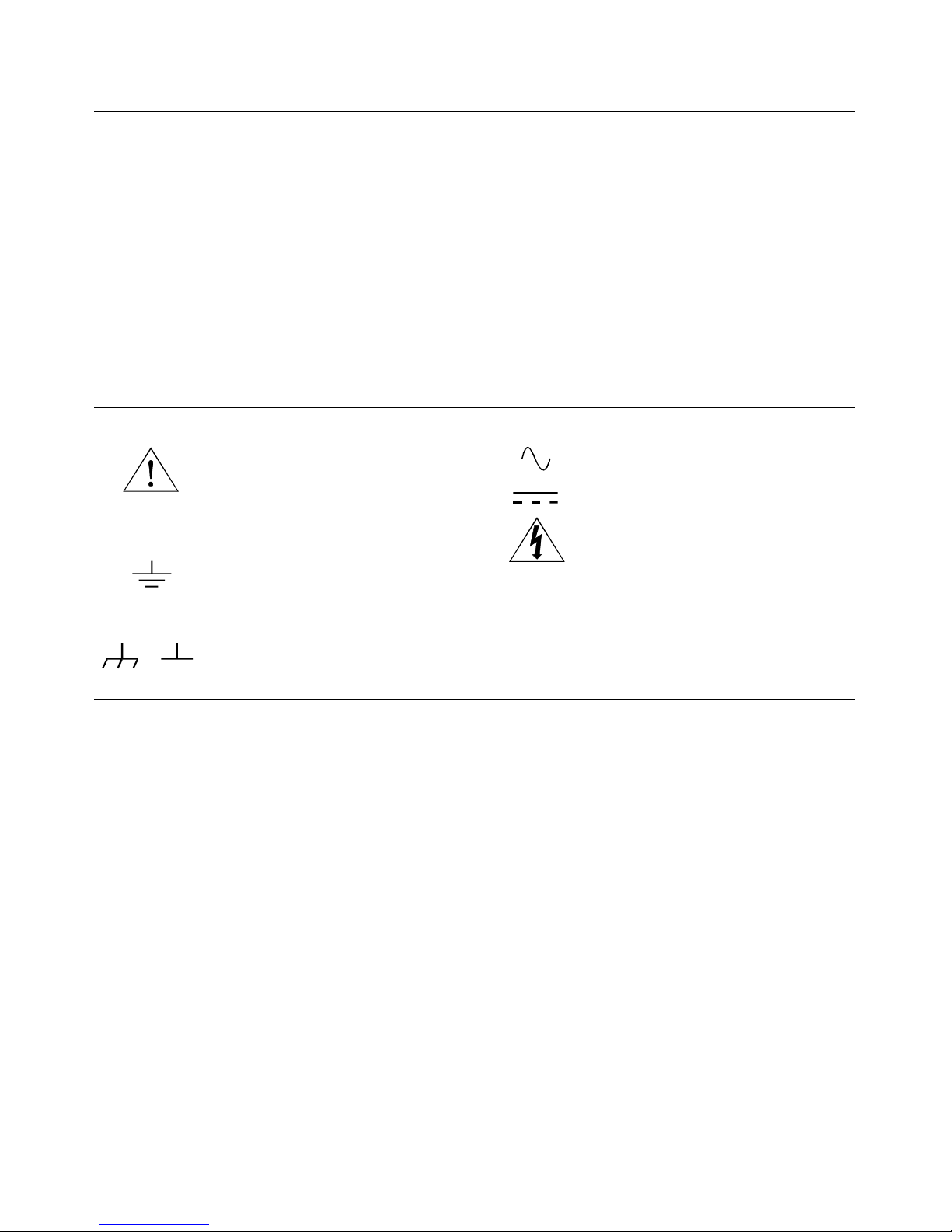
Safety Symbols
Instruction manual symbol affixed to product. Indicat es that the us er must refer t o t he
manual for specific WARNING or CAUTION information to avoid personal injury
or damage to the product.
Indicates the field wiring terminal that must
be connected to earth ground before operating the equipment—protects against electrical shock in case of fault.
Frame or chassis ground termi nal — t ypi-
or
cally connects to the equipment’s metal
frame.
WARNING
CAUTION
Alternating current (AC).
Direct curren t (DC).
Indicate s ha za rdous voltages.
Calls at te nt i on t o a pr ocedure, practi ce, or
condition that could cause bodily injury or
death.
Calls at te nt i on t o a pr ocedure, practi ce, or condition that could possibly cause damage to
equipme nt or perma nen t los s of data.
WARNINGS
The following ge ner al safet y prec aut ions mus t be observed du ring al l phas es of oper ation , ser vice , and repai r of this pr oduct.
Failure to comply with these precautions or with specific warnings elsewhere in this manual violates safety standards of design,
manufacture, and inten ded use of the product. Hewlett-Packar d Company assumes no liability for the cust o mer’s fai lure to
comply with these requirements.
Ground the equipment: For Safety Cl as s 1 equipmen t (equ ipment ha vin g a protective ea rth ter mi nal) , an unint erru ptib le sa fety earth
ground must be provide d from the ma in s power sour ce to the produ ct input wi rin g termi nals or suppli ed power cable .
DO NOT operate the produc t in an explosive at mospher e or in the presen ce of flammable gases or fume s.
For continued protect ion a gainst fire, repl ace the line fuse (s) only with fuse(s) of the same voltage and current rating and type .
DO NOT use repaired fuses or short-circui ted fuse holders.
Keep away from live circuits: Operatin g personnel must not remove equipment covers or shields. Procedures involving the removal
of covers or shields are for use by service-trained personnel onl y. Under certain conditions , danger ous v oltage s m ay exist even with the
equipment switched off. To avoid dangerous ele ctrical shock , DO NOT perf orm procedures involving cover or shield removal unless
you are qualified to do so.
DO NOT operate damaged equipment: Whene ver it i s p ossibl e tha t the sa fe ty protection features bui l t int o thi s pr oduct have been impaired, eithe r t hr ough physical damage, excessive mois t ure , or any other reason, REMOVE POWER and do not use the product until
safe operation can be verified by service-trained personnel. If necessary, return the produ ct to a Hewlett-P ackar d Sale s and Ser vice Office for service and repair to ensure that safety features are maintaine d.
DO NOT service or adjust alon e: Do not attempt internal service or adjustment unless another person, capable of rendering first aid
and resuscitation, is present.
DO NOT substitute parts or modify equipment: Becaus e of the danger of introducin g additional hazards , do not install substitute
parts or perform any unauthorized modifica tion to the product. Retur n the product to a Hewlet t-P ackar d Sales and Ser vice O ffice for
service and repair to ensure that safety features are maintained.
4 HP E1399A Register Based Breadboard Module User’s Manual
Page 5

Declaration of Conformity
according to ISO/IEC Guide 22 and EN 45014
Manufacturer’s Name: Hewlett-Pa ckar d C ompany
Loveland Manufacturing Center
Manufact urer’s Addre s s: 815 14th Street S.W.
Loveland, Colorado 80537
declares, that the product:
Product Name: Register Bas ed Bread boa rd Module
Model Number : E1399A
Produc t Opt ion s: All
conforms to the following Pr od uct Spe cifi cati ons :
Safety: IEC 1010-1 (1990) Incl . Amend 1 (1992) /E N610 10-1 (1993)
CSA C22.2 #1010.1 (1 992)
UL 1244
EMC: CISPR 11:1990/EN55011 (1991): Group1 Class A
IEC 801-2:1991/ E N5008 2-1 (1 992) : 4kVCD, 8k VA D
IEC 801-3:1984/ E N5008 2-1 (1 992) : 3 V/m
IEC 801-4:1988/ E N5008 2-1 (1 992) : 1kV P ower Lin e
.5kV Signal Lines
Supplementary Information: The product her ewi th c ompl ies wit h th e requirements of the Low Voltage Dire ctive
73/23/EEC and the EMC Directive 89/336/ EEC and carri es the CE-mark ing acc ordingly.
Tested in a typical configurat ion in an HP B-Size VXI m ai nframe.
April, 1995 Jim White, QA Manager
European conta ct: Your loca l He wlett-Pa cka rd Sales a nd Servi ce O ffic e or Hewlett- Packa rd GmbH, Departm ent
HQ-TRE, Herr en ber ger Straße 130, D- 71034 Böblingen, Germ any (FAX +49-7031-14-3143).
HP E1399A Register Based Breadboard Module User’s Manual 5
Page 6

Notes
6 HP E1399A Register Based Breadboard Module User’s Manual
Page 7
Please fold and tape for mailing
Reader Comment Sheet
HP E1399A Register Based Breadboard Module U ser’s Manual
Editio n 2
You can help us improve our manual s b y sharing your commen ts and sug gesti ons. In apprec iat ion of your time, we will
enter yo u in a quarterly drawing for a Hewlett -Pac kar d Palmt op Personal Computer (U.S. government employees
cannot participate in the drawing).
Your Name
C ompany Name
Job Title
Address
City, State/Province
Country
Zip/Postal Code
Telephone Number with Area Code
Please list the syste m contr ol ler , oper ati ng syste m, pr ogr a m ming la ng uage, and pl ug-in mo dules you are using.
fold here
BUSINESS REPLY MAIL
FIRST CLASS PERMIT NO. 37 LOVELAND, CO
HEWLETT-PACKARD COMPANY
cut along this line
Measurement Systems Division
Learning Products Department
P.O.Box 301
Loveland, CO 80539-9984
NO POSTAGE
NECESSARY
IF MAILED
IN THE
UNITED STATES
Please penci l-in one circl e for each statement below: Disagree Agree
• The documentation is well organized. OOOOO
•Instructions are easy to understand. OOOOO
•The documentation is clearly written. OOOOO
•Examples are clea r a nd useful. OOOOO
•Illustrati ons are clear and help ful. OOOOO
•The documentation meets my overall expectations. OOOOO
Please write any c omments or sugge stions be l ow--be specific.
fold here
Page 8

8 HP E1399A Register Based Breadboard Module User’s Manual
Page 9

Manual Contents
Chapter 1
HP E1399A Introduction
This manual has three chapters and two appendixes:
• Chapter 1 - Introduction summarizes manu a l c on tents, warran ty
status, and specificati on complia nce. It also includes an over al l
description of the module.
• Chapter 2 - Configuring the HP E1399A describes module
hardware and dimensio ns, an d discusses operation of the backplane
interface circuits on the module. It also provides a typical application
example showing user circuits connected to the backplane interface
circuits.
• Chapter 3 - Using the HP E1399A shows how to use the module in
a VXIbus system.
• Appendix A - HP E1399A Breadboard Specifications lists t he
hardware specifications for the HP E1399A module.
• Appendix B - HP E1399A Parts List/Schematic prov ides HP part
numbers and descriptions of all parts required by the HP E1399A. It
also includes a complete schematic of the E1399 A digital backplane
interface.
Specification Compliance/Warranty
The HP E1399A Breadboard Module is designed in full compliance with
the VMEbus Specificat io n (Revis ion C.1) and the VXIbus specificat ion
(Revision 1.3).
The HP E1399 A warran ty statement, loca ted at the front of th is manual, is
different from the standard Hewlett-Packard warranty for the HP
E1300A/E130 1A mainframe and ot her plug-in modules. Hewlett-Pac kard is
only responsible for defTects in materials and workmanship of the blank
circuit board and supplied hardware.
Warning Hewlett-Packard is not responsible for the performance of your
Chapter 1 HP E1399A Introduction 9
custom-designed circuitry. Hewlett-Packard is not responsible
for damage to or improper operation of your VXI mainframe or
other plug-in modules caused by the HP E1399A Breadboard
Module.
Page 10

HP E1399A Description
The HP E1399A Breadboard Module is a B-size register-based device that
provides a convenient interface to a VXI mainframe backplane. It allows
you to construct your own custom hardware for use wit h the mainframe.
General Module
Features
Back plane Interf ac e
Feat u res
Note For hardware operation, a mnemonic suffixed with an asterisk (such as
The module is supplied with all interface components loaded and soldered.
Your VXI mainframe can communicate with this module configured as an
A16/D16 device. The breadboard module interface circuitry is implemented
and accessible according to the requirements outlined in the VXIbus
Specification.
Users can still provide cus t om ex tensions to expand module add ressing
capability to A24 or A32 by adding approp riate circuitry according to the
VMEbus and VXIbus specificatio ns.
An overview of the HP E1399 A interface features follows. Figure 1-1
shows a block diagram of this interface.
WRITE *) indicat es invers e lo gic (0 or low = true; 1 or high = false). A high
state (1) is defined as a positive voltage (usually +5 V) and a low state (0) is
defined as zero V (ground) at the specified signal point.
The HP E1399A interface features are:
• Address Lines and Register Decoding. The module implements 15
address lines (A1-A15) to all ow for: 1. decodi ng one of 255
switch-selectable logical device addresses in the upper fourth of the
A16 VME address space, and 2. selecting one of the breadboard
configuration registers for read/write operations. The module
decodes the Address M odif ier lines AM 0 - AM5 and acts on codes
and 2D16 only.
29
16
• Data Lines. Data lines D0-D15 are available for use on the
Breadboard module. These 16 lines are buffered by data bus drivers
and used for writing to, and reading from, the configuration registers
(Status, ID, Device Type, and Control) via a n internal data bus
(DB0-DB15).
10 HP E1399A Introduction Chapter 1
Page 11
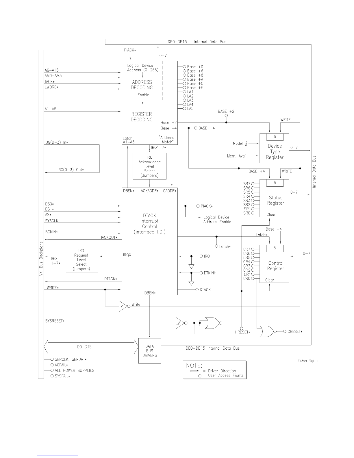
Figure 1-1. Digital Backp lane Interface Block Diag ra m
Chapter 1 HP E1399A Introduction 11
Page 12

• Status Register. A read of this 8-bit register provides inform ation
about the status o f t he bre adboard module. Implemented signals are
"Extended*" and "Passed". There ar e also p r o visions for
implementing device-dependent sta tus bits.
• ID Register. A read of this 16-bit register identifies the
Manufacture r ID number, th e Devic e Class, and the addressing mode
of the Breadboard. This register is implemented as a
Hewlett-Packard A 16 r egister bassed device.
• Device Type Register. A read of this 8-bit register identifies the
unique ca r d mo del as defined by the de v i ce man u f acturer. T he car d
model nu mb er is switc h selecta b le.
• Control Register. A write to this 8-bit register causes specific
actions to be executed by the device. "Reset" and "System Fail
Inhibit" are implemented. Other device-depend ent control bits may
be impleme nted by the user.
• Read/Write Operations. Using the backplane interface circuitry
provided, it is possibl e to read the contents of t he Status, ID, or
Device Typ e Registers ont o the data bus (D0- D15), or to write
information in to the Control Register from the data bus.
• DTACK. The interface contains the circuitry required for generating
a delayed DTACK* (data transfer acknowledge) signal.
• Interrupt Interface. The breadboard module has D16 interrupter
capability. It do es not contain an int errupt handle r. Interrupt pri ority
is jumper-selectable for pulling the appropria t e int errupt r eq u est line
IRQ1* - IRQ7*. Interrupts are gen erat ed by t he IRQ state machine
on the Interface IC (U6). The daisy-chained IACKIN*/IACKOUT*
signal pair is implemented.
• Module Reset. Both hardware and software reset signals are
provided to initialize the backplane interface circuitry and your own
custom-designed circuitry to a known state.
• Backplane Buffering. Buffering is provided for all signals that
interface with the VXIbus backplane.
• Power Supply. The following power supply voltages (all unfiltered)
are available:
– +5 VDC, fused at 4 Amps
– + 12VAC, fus ed at 4 Amps
– -12VAC, unfused
– +5VDC standby, unfused
12 HP E1399A Introduction Chapter 1
Page 13

HP E1 399A
Hardware Feat ure s
An overview of the HP E1399 A hardware features follows.
• Connectors. Two 96-pin DIN connectors are provided with the
module. P1 connects to the VXI backplane, while J1 allows
connectio n of devices from the front of the board, or co nnect ion of
an E1399A terminal card.
• Co mponent Area. An ar ea of ap pr ox ima tely 220 cm
available on the module to install your own custom circuitry. This
area does not include the portion of the circuit board r equired by the
backplane interface components.
2
(34 in2) is
• Component Heig ht/ L ead Le ngth. The maximum component height
allowed ab ove the circuit board is 12.7 mm (0.5 in). The maximum
component lea d length allowed below the circuit board is 1.3mm
(0.05 in).
Warning Since the inputs to the HP1399A Breadboard Module are
through a 96-pin connector and a terminal card assembly, limit
voltage to 250Vdc/250Vrms .
Chapter 1 HP E1399A Introduction 13
Page 14

14 HP E1399A Introduction Chapter 1
Page 15

This Chapter contains a detailed hardware description of the breadboard
module and discu sses the backplane interface circuitry. It also s hows a
sample application to control 16 relays on the module.
Handling Precautions
WARNINGS, CAUTIONS, and guidelines to reduce the risk of static
discharge damage to the HP E1399A follow.
Warning SHOCK HAZARD. Only qualified, service-trained personnel who
are aware of the hazards involved should install, remove, or
configure any module. Before removing any installed module,
turn off all power to the mainframe and to all external devices
connected to the mainframe or to any of the modules.
Chapter 2
Configuring the HP E1399A
For electrical shock protection, ensure that the module face
plate is securely tightened against the mainframe.
Warning Since the inputs to the HP 1399A Breadboard Module are
through a 96 pin connector and a terminal card assembly, limit
voltage to 250Vdc/250Vrms .
Caution STATIC SENSITIV ITY. The back p lane interfac e circu itr y
described in this Chapter uses static-sensitive CMOS
integrated circuit devices. If you implement the circuitry
described herein, you must use clean-handling and anti-static
techniques when handling the module to protect the sensitive
components from damage due to electro-static discharge (ESD).
Chapter 2 Configuring the HP E1399A 15
Page 16

Redu cing Ri sk of
Static Dis charg e
Damage
The smallest static voltage most people can feel is about 3500 V. It takes
less than one-tenth of that (about 300 V) to destroy or severely damage
static-sensitive circuits. Often, static damage does not immediately cause a
malfunction, but significantly reduces the component’s life. Adhering to the
follo wing precautions will redu ce the risk of static disc harge da ma ge .
• Keep the module in its conductive plastic bag when not installed in a
VXIbus mainframe. Save the bag for future module storage.
• Before handling the module, select a work area where potential static
sources are minimized. Avoid working in carpeted areas and
non-conductive chairs. Keep body movement to a minimum. If
possible, use a static-controlled workstation.
• Avoid touching an y components or edge connectors. When you are
ready to configure the module, remove it from its protective bag and
lay it on top of the bag while keeping your free hand in contact with
the bag. This t ec hnique maintains you r b ody and the module at t he
same static potential.
• When you install the module, keep one hand in contact with the
protective bag as you pick up the mo dule with your other hand.
Then, b efor e insta lling the module, move your free hand to a me ta l
surface on th e mainframe, t hus bringing you, th e module, and the
mainframe to the same static potential.
Hardware Description
Figure 2-1 shows the module with interface circuit components installed. As
shown, the module consists of a circuit board with one backplane connector
(P1) and a front pan el connector (J1). Approximately one-third of the circuit
board contains traces for installing the backplane interface circuitry. See
"Backplane Interface Circuitry" for interface circuitry installation.
Backplan e
Connections
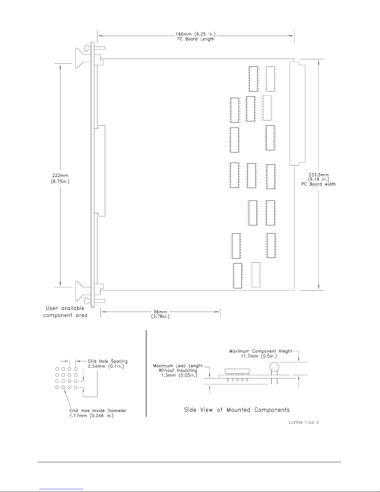
Module Dimensions Figure 2-2 shows the dimensi ons of the module and the compone nt heig ht
The breadboard module interfaces your custom circuits to a standard B-size
VXIbus backplane (connector P1). This enables you to access the backplane
control signals, data lin es, address lines, and power suppli es. Figure 2-1
shows backplane connect or (P1) which connects to the VXIbus backplane.
and lead length restrictions. The maximum component height allowed
above the circuit board is 12.7mm (0.5in). The maximum c ompon ent lead
length allowed below the circu it board is 1.3mm (0.05in). Do not mo unt
components closer than 4mm (0.16in) to the extreme upper or lower edges
of the circuit board. This space is used to guide the module into the
mai nframe m odu le slo t . An area o f 2 2 0 c m
module to install your own circuitry.
2
(34 in2) is availab l e on the
16 Configuring the HP E1399A Chapter 2
Page 17
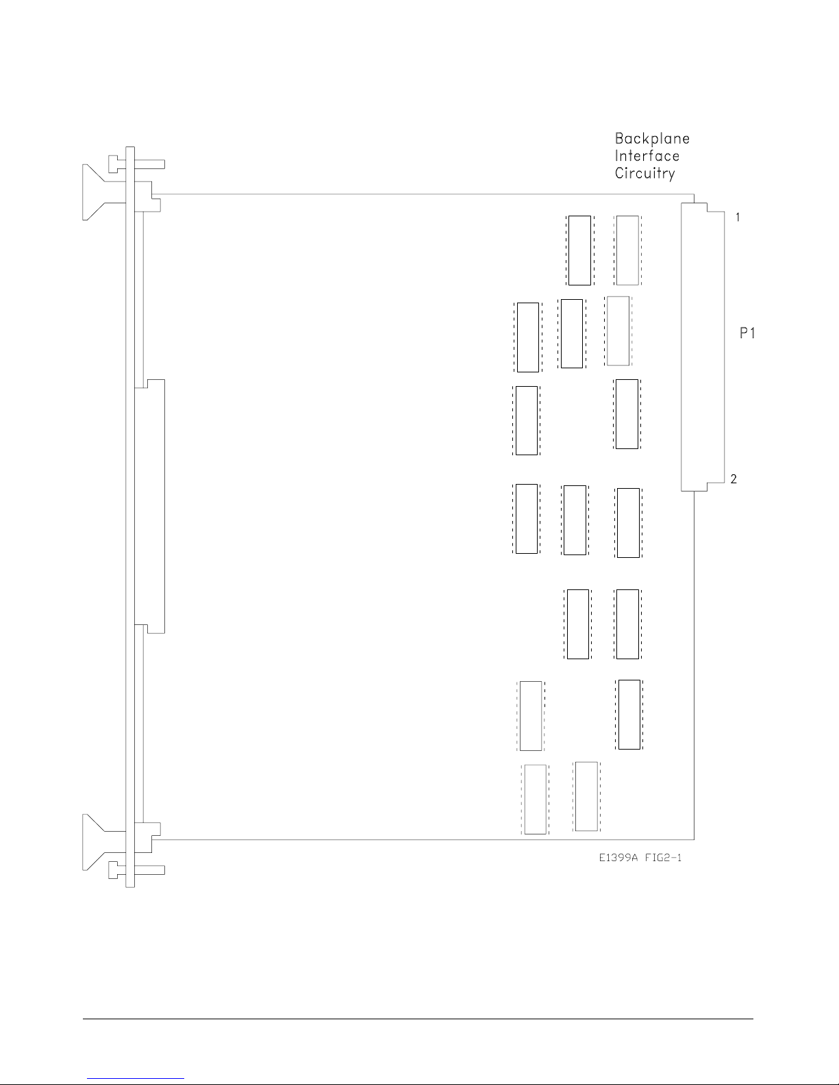
Figure 2-1. HP E1399A Breadboard Module & Connecto r Pinou t
Chapter 2 Configuring the HP E1399A 17
Page 18
18 Configuring the HP E1399A Chapter 2
Figure 2-2. HP E1399A Dimen sions
Page 19

Cooling
Requirement s
Note It is the user’s responsibility to furnish ade quate cooling f or a n y module to
The V XIbu s Specific at ion req uir e s mod ule ma n u f act urer s to estab l i s h a
cooling specification for each of their modules. The specification is to
consist of: (1) the airf low required (in liters/s eco nd) for ade qua te cooling,
and (2) the pressure drop that oc curs across the module when th e specified
airflow is applied.
be used in a VXIbus system. Module cooling requirements are described in
the VXIbus Specification (Rev 1.3) in Section B.7.2.4. Mainframe cooling
requirements are discussed in Section B.7.3.5.
For ease of integration, you should label the airflow requirements for your
finish ed app lication circu it r y o n t he mod ule. For example, the label might
read: 0. 3 liters / s ec @ 0. 2 m m/ H
O.
2
Due to the nature of a breadboard module, it is not possible to specify
cooling requirements without knowing the application and the amount of
power to be dissipated. Given the application, however, cooling
requirements may be estimated as f ollo ws:
1. Determine the airflow required as a function of po wer diss ipation. To
maintain a 1 0ºC r ise, approxima tely 0.08 lit ers/ s econd are required
for every watt dissipat ed. For exa mp le, if a module dissipates 20
watts, 1.6 liter/second of airflow is required for cooling.
2. Establish the relationship between a ir flow and pr e ssure drop. For a
breadboard loaded with typical components (such as ICs, relays, and
a few heat sinks), the curve i n Figure 2-3 may b e us ed to de termine
the pressure drop across t he module. Determine th e p ressure drop as
the intersection of the curve and the required airflow. For example, if
the airflow required is 1.6 liter/second, th e pressure drop across a
typically populated breadboard will be approximately 0.05 mm H
O.
2
Chapter 2 Configuring the HP E1399A 19
Figure 2-3. Pressure vs. Airflo w
Page 20

Terminal Module An optional terminal module is available for making external connections to
the HP 1399A Breadb oar d Module. This modul e consists of a connec tor
mounted on a breadboard so that you can access the connector pins by
soldering wires to the breadboard. Figure 2-4 shows the layout of this
terminal module. Figure 2-5 shows h ow to make the connections and ins ta ll
the mo dule.
Warning Since the inputs to the HP 1399A Breadboard Module are
through a 96-pin connector and a terminal card assembly, limit
voltage to 250Vdc/250Vrms .
For electrical shock protection, ensure that the module face
plate is securely tightened against the mainframe before
installing the termina l card.
20 Configuring the HP E1399A Chapter 2
Figure 2-4. Terminal Module Assembly
Page 21

Chapter 2 Configuring the HP E1399A 21
Figure 2-5. Termin al Mo du le Instal lati o n
Page 22

Backplane Interface Circuitry
The backplane interface circuitry allows you to access the backplane control
signals, data l ines, address lines, and power supplies. Approxi mately
one-fourt h of t he circuit board is reserved for insta lling the backp lane
interface components. All of the components required for the interface are
provided with the modul e and are already loaded and tested. Your VXIbus
mainframe can communicate with the HP E1399A in a manner similar to
other VXIbus plug-in modules. The backplane interface circuitry consists of
the following functional groups:
• Address Lines and Register Decoding
• Data Bus Drivers
• Statu s Register
• ID Register
• Device Type Register
• Control Register
• DTACK, Interrupt and Cont rol
• Backplane Signals and Voltages Availab le on the Module
The following sections discuss the backplane interface functional groups.
Each section includes a description, partial schematics, timing diagrams
(where applicable), and a parts list showing the components required by that
group. See Appendix B, "HP E1399A Parts List/Schematic" for a complete
parts list, and for a schematic of the entire backplane interface.
Note In the discussions o f hardwa r e op eration that follo w, a high state (1) is
Address Li nes and
Register Decoding
indicated by a positive voltage (usually +5 V) and a low state (0) is
indicated by zero V (ground) at the specified signal point. A mnemonic
suffixed with an asterisk (such as WRITE*) indicates inverse logic (0 or
low = true; 1 or high = false).
Figure 2-6 shows the address line and regist er decodi ng circuitry, while
Table 2-1 shows the applicab le parts list. The HP E1399 A Breadboard
Module is desi gned to b e us ed as an A16/D1 6 de vice. As such, only
backplane address lin es A1-A15 and data lines D0-D15 have been
implemented on the module.
To address the module, the information present on backplane lines A6-A13
must be identical to the logical address as set by address switch SP1(0-7).
These eight bits allow up to 255 diff erent VXIbus logical devices to be
selected on a VXIbus system.
22 Configuring the HP E1399A Chapter 2
Page 23

Table 2-1. Address Lines and Register Decod i ng Parts
Reference
Designator
RP25
SP1
U11
U20A, 9C
U17, 18
U7, 8
U15
HP Part Number Description
1810-0279
3101-3066
1820-3975
1820-4242
1820-3631
1820-3079
1820-4147
Resistor, Networ k, 9-b y- 4.7kOhms
Switch, DIP, 8 rocker 0.05 A, 3 0 VD C
IC, 74HC541 Octal Line Driver
IC, 74HCT14, Schmi tt Trigger Invert e r
IC, 74HCT688N 8-bit Magnitude Comparator
IC, 74HC138N 3-to-8 Line Decoder
IC, 74HCT573 Octal D-Ty p e Latch
Figure 2-6. Address Lines and Regi ster Decod ing
Chapter 2 Configuring the HP E1399A 23
Page 24

If a logical address m atch o ccurs a nd IACK* is high (fals e), equali ty
detector U18 produ ce s a low at its output wh ich enab les U17. Next, equality
detector U17 c ompar es t he inform ation on ba ckp lane lines A14, A15, AM0 ,
AM1, and AM3- AM5 to a hardwire d code of 11101X01
. Since AM2 is not
2
examined, this hard-wired cod e wil l b e a mat c h if a ll three of th e following
conditions are true:
• a hexadecimal cod e of either 29
or 2D16 is pres ent on lines
l6
AM0-AM5.
• A14 and A15 are both high (1).
• LWORD* is high (false).
Either of the two address mo difier h exad ecimal co des indi cat ed above will
establish A16 addressing per the VXIbus Specification (Section C.2.1.1.4).
In the VXIbus addressing scheme for an A16 device, A14 and A15 are
always set to 1 to select the upper 16K of the 64K A16 address spac e (per
the VXIbus Specification, Sections A.2.3 .3 and C.2.1. 1.1). LWOR D* is
high (false) when decoding short word transfers.
If a second match occurs at U17, its ou tput goes low. This triggers a data
transfer cycle using the DTACK state machine in the Interface IC (U6) by
the low at U6 input CADDR* (See "DTACK, Interrupt, and Control" for
more information on the DTACK state machine). As part of the data
transfer cycle, U6 sets DBEN* low (true), latching the remaining backplane
address lines (A1-A5) at the U15 outputs to the two 3-to-8-line decoders
(U7 and U8).
Latch U15 ensures that the data is held valid until the data strobes go high
(false) even t hou gh t he a ddre ss lines may no longer be valid.
U8 is enabled if G1 is high and both G2A and G2B are low. Therefore, A4
and A5 must both be low to select a register for connection to the data bus
(D0-D15). G1 will be high (via U9C) if there was a match at U17. If U8 is
enabled, backplane lines A1-A3 are decoded to specify which register
(Status, ID, Device Type, o r Control) is to be connect ed t o the data bus.
Other user-supplied registers can be selected also. If additional decoding is
necessary, A 4 a nd A5 a re accessible on the module. See Table 2-2 and
Figure 2-6, for information on implemen t ing y our own register selections.
24 Configuring the HP E1399A Chapter 2
Page 25

Table 2-2. 1 Register Selectio n
A3 A2 A1 Enable Lin e Register
0 0 0
0 0 1
0 1 0
0 1 1
1 0 0
1 0 1
1 1 0
1 1 1
Base + 0
Base + 2
Base + 4
Base + 6
Base + 8
Base + A
Base + C
Base + E
ID
Device Type
Status/Control
User Assignabl e
User Assignabl e
User Assignabl e
User Assignabl e
User Assignabl e
Data Bus Drivers The HP E1399A Breadboard Module is designed to be used as an A16 and a
D16 device only. As such, only backplane address lines A1-A15 and data
lines D0-D15 have been imp lemen t ed on the module.
VXIbus backplane connector P1 contains 16 bi-directional data lines
labeled D0 t hrou gh D15. The breadboa r d module connects to these data
lines using the c ircuitry shown in Figur e 2-7 (Tab le 2-3 show s the Data Bus
Drivers part s list ). Da ta buf fering is pr ovided for the data lines by two
tri-stat e octal bus transceivers. U16 buffers D0 through D7 and U35 buffers
D8 through D15. Note that the data lines are labeled DB0 through DB15 on
the module side of the buffers.
U16 and U35 are enabled during a data bus transfer cycle when DBEN*
(Data Bus Enable) goes low (true). This occurs when ever the breadboard is
correctly addressed by a match of the module’s logical address as set by
SP1(0-7).
The direction of data transfer is determined by WRITE*. When WRIT E* is
low (a "write" operation), information present on backplane lines D0-D15 is
transferred to the breadboard Control Register via DB0-DB15. W hen
WRITE* is high (a "read" operation), information present on DB0-DB15 is
transferred to backplane lines D0-D15.
Note WRITE* is the signal availab le on the VXI bus backplane. This signal is
converted immediately to WRITE via U20F (schmidt trigger inverter). The
signal accessibl e to the user on the breadboard is WRITE, not WRITE*.
During a normal read operation, the information present on DB0-DB15 is
selected by the Address Decode circuitry from one of two sources:
• Statu s Register (U14 )
• Device Type Register (U10)
You can also write to or read from up to five more device-dependent
registers using the extra enable lines provided. Refer to Table 2-2 and to
Figure 2-6 to s ee the us er-as signa ble enable lines.
Chapter 2 Configuring the HP E1399A 25
Page 26

Table 2-3. Data Bus Drivers Parts
Reference
Designator
RP26,32
U16,35
HP Part
Number
1810-0279
1820-3714
Description
Resistor N etwork , 9- by 4. 7kO h m
IC, 74ALS245A-1 Oct al Bus Tr nsc vr, TTL
Status Register The Status Register is an 8-bit register which provides some specific status
information (as defined by the VXIbus Specificati on), and wh ic h has other
bits available for custom (device dependent) status information as
implemented by the user.
Figure 2-7. Data Bus Drivers
Table 2-4 s hows the sta tus r e gister bit d efin itions. See Chapt er 3, "Using the
HP E1399A" for additional information on usin g the status register. Refer to
the VXIbus Sp ecification, Section C.2.1.1. 2, for detailed information
concerning status r egister implementation restrictions.
Table 2-4. Status Register Bit Defin itio ns
Data Bit(s) Definitions
SR0 - SR1
SR2
SR3
SR4 - SR7
Device Dependent (User assignable)
(0=Failed/Executing Self-test, 1=Passed Self-test)
(If 0, and Pas sed bit = 1, Extended Self-test active)
Device Dependent (User assignable)
As shown in Figure 2-8, the status register circuitry consists primaril y of the
data bus line Driver U14, and a resistor network. Tab le 2-5 show s the parts
list for th e status reg ist er.
The status register is enabl ed dur ing a "r e ad status register" operation by t he
BASE+4 enab le line set low (decoded from a ddre ss lines A1-A3), and b y
26 Configuring the HP E1399A Chapter 2
Page 27

WRITE* set high (false). The information presented to U14 by status lines
SR0-SR7 is placed on the internal data bus (DB0-DB7). The user must
provide any latches required to latch and hold this information.
Table 2-5. Status Register Parts
Device Type
Register
Reference
Designator
RP2
U14
HP Part Number Description
1810-0279
1820-3975
Resistor N etwork , 9- by 4. 7kO h m
IC, 74HC541 Octal Line Driver
The Device Type Register is an 8-bit register which contains a
device-dep endent "module type" identifier. This field is set on the module
by the use of an 8-position DIP switch on the inputs to the data bus line
driver U10, as shown in Figure 2-9. Table 2-7 shows the resistor and IC part
numb ers for a Devic e Type Register.
Figure 2-8. Status Register
Chapter 2 Configuring the HP E1399A 27
Page 28

Table 2-6. Devi ce Type Register Bit Definition s
Data Bit( s) Definit io ns
DB0-DB7
DB8-DB15
Devic e Type or Model Code (Range = 0-409 5)
Set to "1"
Table 2-7. Device Type Register Parts
Refer e n ce
Designat or
RP1
U10
SP2
HP Part Number Description
1810-0279
1820-3975
3101-3066
Resistor Network, 9- by 4.7kOhm
IC, 74HC541 Octal Line Driver
Switch,DIP,8-Rocker .OSA 30V D C
Each bit in the Device Type Regist er is normally pulled hi gh (1) by RP1.
Figure 2-9. Device Type Register
The bits can be reconfigured using the DIP switch. The range of device
types for an A 24 or A 32 de vice is 0 - 4095. For a n A16 device, a l l 16 b its
are availab le for specifying the device type for a range of 0- 65 535. The
user will need to add the required buffer and resistor network to implement
the full A16 device type range. The default factory setting is FFxxh.
Note Per the VXIbus Specification (OBSERVATION C.2.6), device types 0-255
are reserved for register-bas ed S l ot 0 d e v ices.
Refer to the VXIbus Specification, Section C.2.1.1.2 for detailed
information concerning Device Type Register implementation restrictions.
Table 2-6 shows the D evice Type Register bit definitions.
28 Configuring the HP E1399A Chapter 2
Page 29

Control Register The Control Register is an 8-bit register which causes specific actions to be
executed by the breadboard module when written to from the backplane
data bus. The pr ima r y component of t he C ontrol Register is U13, as shown
in Figure 2-10. Tab le 2 -9 show s the part number for U13.
Table 2- 8. Contro l Register Bit Defin itio ns
Data Bit(s) Definitions
CR0
CR1
CR2-CR7
Reference
Designator
U13 1820-4086 IC, 74H( T~73 Octal D-Type Flip Flop
CRESET (software reset)
SYSFAIL INHIBIT
Device Dependent (User assignable)
Table 2-9. Control Regist er Parts
HP Part Number Description
Chapter 2 Configuring the HP E1399A 29
Figure 2-10. Control Register
Table 2-8 shows the Contr o l Register bit definitions. The Control Register
is selected f or writing to b y t he BAS E+4 e na ble line (see Table 2-2).
BASE+4 going lo w at the input of U21C, combined with a negative pulse
(for on e clock c yc le of SYSC LK) from the LATCH* output of U6 (also
applied to U21C), provides a positive-going edge clocking pulse
(CONTROL ) to U13. This pulse clocks whatever is present on DB0-DB7
through U15 to the Control Regist er access points (CR0 -CR7 ).
Page 30

Users may connect any or all of these points to custom circuitry, keeping in
mind the pre-defined bit assignments shown in Table 2-2. Data present on
DB0-DB7 would have been written there by the same DTACK state
machine data transfer cycle that provided the LATCH pulse. See "DTACK"
for a discussion of the DTACK state mac hine operation.
See Chapter 3, "Using the HP E1399A" for additional information on using
the Control Reg ister. Refer t o the VXIbus S pecification, Section C.2.1. 1. 2
for detailed information concerning Control Register implementation
restrictions.
DTACK, Interru pt,
and Control
DTACK The Data Transfer ACKnowledge (DTACK) circuitry is c entered arou n d
An Interface IC (U6) provides the timing and control signals for standard
data transfer cycles and interrupt requ ests/a cknowledgments. Hardw a re and
software reset signals, together with a card fail signal, have also been
implemented.
the Interface IC (U6). A state machine in this IC controls all read and write
data transfer cycles. Operation begins with the state machine in the idle
state. See Figure 2-11 f or the fo llowi ng discu ss ion. Table 2-10 lists the parts
for the DTACK circuitry.
Table 2-10. DTACK Circuitry Parts
Refer e n ce
Designat or
U21C
U6
U5C
U20C,D,F
HP Part Number Description
1820 464 3
1820-6731
1820-4057
1820-4242
IC, 74HCT02N Quad 2-input NOR
IC, Interface (PAL)
IC, 74F38N Quad 2-input NAND Buff er
IC, 74HCT14 Hex Schmitt-Trig Invrtr
30 Configuring the HP E1399A Chapter 2
Figure 2-11. DTACK Circui try
Page 31

In the first part of the transfer cycle, the system controller places the address
of the breadboa r d modu le o n the back plane address (A1-A15), address
modifier ( AM0-AM5), an d address strobe ( AS*) lines, and th en sets the
appropriate data strobe lines low (DS0* and DS1* for a D16 device). When
the address equality det ectors (U17, U18) detect the address match, th e
output of U17 goes low.
This low is sensed at the Card ADDRess (CADDR*) input to U6 which,
together with the active data strobes, tells the DTACK state machine in the
Interface IC (U6) that the module has been addressed for a data transfer
cycle. This starts the state machin e, with all signals being clocked by
SYSCLK (16 MHz).
In the first active state, the data bus drivers (U16,U35) are enabled and the
register-specifier part of the address (A1-A5) is latched onto the outputs of
U15 using the Data Bus ENable (DBEN *) output of U1. If the data transfer
cycle is a read o p erati on (as indicated by WRITE * high), the decoded
output of U8 det ermines which one of the registers (Status, ID, or Device
Type) is enabled to put its contents onto the module’s internal data bus
(DB0-DB15).
The next stat e then gene ra t es a high at the DTACK out put of U 6. This
forces DTACK * low (true) on the backplane through U5C, acknowledging
to the system controller that the module has received the request for data
and has plac ed the co ntents of t he specified register onto the data lines.
With U16 and U35 enabled, internal data lines DB0-DB15 are connected
directly to the backplane data lines D0-D15.
If the data transfer cycle is a write operation (as indicated by WRITE* low),
an additional state sets the U1 LATCH output low (enabling the Control
Register to receive data from the data bus drivers) before DTACK* is set
low (tru e). The r es ulting Control Register outputs (CR0-CR15) can t he n
control t h e u ser’s circ uits, as desired. A gain, DTA CK* going low (tru e)
tells the system controller that the data transfer cycle is complete. In a write
operation, WRITE * going l ow (true) disables the Status R egist er, the ID
Register, and the Device Type Register.
For both read and write operations, the DTACK state machine holds
DTACK* low and the address latched until the data strobes are invalid.
After the data strobes go invalid, the data bus drivers are disab l ed and the
address latc h is rele as ed. In the next state, DTACK* is releas ed and t he state
machine returns to the idle state. If the DTACK INHibit signal (DTKINH)
is set high (it is wire jumpered low on the HP E1399A implementat i on), it
allows the user to hold the state machine in the first state of latched address
and enabled data bus dr ivers.
Chapter 2 Configuring the HP E1399A 31
Page 32

Interrupt A priority interrupt scheme has been implemented using the Interface IC
(U6). Anot her stat e mach ine co ntrols int errupt r eq u est and acknowledg e
operations. See Figure 2-12 for the following discussion. Table 2-11 lists
the parts for the Interrupt Circuitry.
Table 2-11 Interrupt Circuitry Parts
Reference
Designat or
U21C
U6
U5A,B,C
U20B,C, D, F
HP Part Number Description
1820-464 3
1820-673 1
1820-405 7
1820-424 2
IC, 74HCT02N Quad 2-input NOR Gate
IC, Interface (PAL)
74F38N Quad 2-input NAND Buffer
IC, 74HCT14 Hex Schmitt-Trig Invrtr
The VMEbus interrupt r equest levels IRQ1*-IRQ7* are jumpe r-se l ect abl e
32 Configuring the HP E1399A Chapter 2
Figure 2-12. Interrupt Circu itr y
(only one at a time allowed) for both the IRQ requ est output line
(IRQ1*-IRQ7$) and the IRQ acknowledge input line ( ACKADDR*). IRQ
request and acknowledge levels must always be the same (IRQ1* is shown
select ed in Fi gure 2-1 2). T o ge ne r a te an interrupt reques t t o the int err upt
handl er and start t he IRQ sta te machin e in U6, t he user’s custom circuits
must provide a high signal at th e IRQ access point input to U6
(ACKADDR).
Page 33

The IRQ stat e machine monitors th e f ollowing interrupt-related lines t o
determine its actions: IACK*, valid DS0*, IACKIN*, AS*, ACKADDR*.
If the module is asserting IRQ and the int errupt-related lines are in the
proper state, the IRQ state machine asserts IRQX high (true) on U6.
IRQX high (true), inve r ted by USA, pulls th e jump er- s elected IR Q1* line
low (tru e) on the backplane . The state mac hine then waits for the interrupt
handl er to recognize the interrupt r e quest. W hen t he int err upt handler
responds, it plac es the code for the interrupt request priority level that it is
acknowledg ing onto lines A1-A3. It then sets IACK* low (true) which sets
IACKIN* low (true).
IACK* low (true) sta r ts the interrupt acknowledge cycle, disab ling normal
address decoding on the breadboard module. When IACKIN* goes low
(true), t he IRQ sta te machine checks to see if its own IRQ le ve l ha s been
acknowledged (input line ACKADDR at U1 will be set low by a correct
match of U7’s de coded output and the jumper s election for IRQ
ACKNOWLEDGE).
If its own level is not being acknowledged, or if the module is not asserting
IRQ, the stat e machine passes the daisy-chained IACKIN* signal through
IACKOUT on U6. The IACKOUT signal is gated with an inverted AS* to
meet release time requirements for IACKOUT* as outlined in the VMEbus
Specification.
If the acknowledge level matches the request level, the IRQ state machine
sets PIACK* low (true), releases IRQX (and IRQ1*) and starts the DTACK
state machine for a read cycle. The interrupt handler initiates the read cycle
to get the logical device address from the interrupter when it sees IRQ1 * go
low ( true). PIACK* low ( t rue) en ab les U11 to plac e t he modu le’s log ica l
address (from SP1 ) o nto the lower eight bits of the internal data bus
(DB0-DB7).
The logical address is then transferred to backplane lines D0-D7 during the
read data transf er cycle. In th is way, the i nterrupt handler knows which
device is asserting IRQ if more than one device has the same interrupt
prio rity assig ned t o i t.
Chapter 2 Configuring the HP E1399A 33
Page 34

Control Table 2-12 sho ws the co ntrol s i gnals which are impl ement ed (s ee the
"Backplane Interface Schematic" in Appendix B):
Table 2- 12. Control Signals
Signal Definition
AS*
DSO*, DS1*
SYSCLK
SYSFAIL*
SYSRESET*
Address strobe, used in data transfer cyc les.
Data st robes, us ed in t he data transfer cycle s.
Provides 16-M H z clock sign als to Interf ac e IC (U6) for clock in g the
state machines.
SYSFAIL input. If the SYSFAIL INHBT lin e output of th e Control
Register (CR1) is also low (not inhibited), th en SYSFAIL* is asserted.
System reset signal , norm all y used to initi alize the backplane
interface circuitry (and your own custom circui ts) to a known state.
Provides a hardware reset capability. As implem en ted (HRESET* ), it
clears the Status Register and th e Control Regist er. It also asserts
the software reset line (access point CRESET* on the module).
CRESET* can also be asserted via software by writing a high signal
to the Control Register (access point CR0), providing an input to
U21D.
34 Configuring the HP E1399A Chapter 2
Page 35

User Access Points The breadboar d module contains tra c es (stubs) f or accessing many of the
signal lines on backplane connector P1. Table 2-13 shows the signal lines
that are brought onto the module but not implemented. They are available as
signal access points for your custom circuits.
Table 2-14 shows all of the impl emented signal lines available as access
points, e it her as i nput s from the backplane to your own cust om c irc u itry, or
as outputs to the backplane from your custom circuits.
Table 2-13. User Access Points (Stubs)
Signal Lines Description
ACFAIL*
BERR*
SERCLK
SERDAT*
Table 2-14. User Access Points (Implemented Signal s)
A1-A5
BASE+0
BASE+2
BASE+4
BASE+6
BASE+8
BASE+A
BASE+C
BASE+E
CR2-CR7
DB0-DB15
DS0 & DS1
SR0, SR1
SR2
SR3
SR4-SR7
DBEN*
CRESET*
DTACK
DTACK INH
AS
SYSFAIL
SYSFAIL INH
HRESET*
IRQ
LATCH*
PIACK*
CADDR
AC Input Power failure
Bus ERRor signal
Synchronizes data transmission on the VMSbus
Used for VMSbus data transmission
Backplane address lines A1-A5 (latched)
ID Register Enable line
Device Type R egister Enabl e l ine
Status and Control R egister s Enable li n e
User-assignable Enable line
User-assignable Enable line
User-assignable Enable line
User-assignable Enable line
User-assignable Enable line
Control Regis ter out pu t lin es
Breadboard Module internal Data Bus lin es
Buffered data strobes
Statu s Regist e r (pul l ed u p )
Statu s Regist e r (pul l ed u p )
Statu s Regist e r (pul l ed u p )
Statu s Regist e r (pul l ed u p )
Data bus buffer enab l e
Card RESET, software (CRO ) or hardware (SYSRESET*)
Data Transfer ACKnowledge (DTACK high = DTACK* low)
DTACK INHibit
Buffered address strobe
Card failure signal (jumpered to GND)
SYSFAIL INHibit (jump ered to GND)
Hardware RESET (from SYSRESET*)
Interrupt ReQuest line, User-implem ent ed j um per to ground
Latches data into write registers
Peripheral Interrupt ACKnowledge line
Card ADDRess match
Chapter 2 Configuring the HP E1399A 35
Page 36

Power Supplies All of the power pins on P1 (as shown in Table 2-15) are available on short
stubs from the connectors. The +5 VDC and +12 VDC power supplies ar e
fused. Users should fuse and filter any other power supplies they access to
protect their mainframe.
All ground pins are connected together and are accessible in several places.
No ground loop s are pr es ent in t he module. The front pa nel of the module is
not grounded.
Table 2-15. Power Su p ply Voltag es and Pin Numb er s
Voltage Connector and Pin Numbers
+5 V dc
+5V stdby
+ 12 V dc
-12 V dc
(P1) A32, B32, C3 2
(P1) B31
(P1) C31
(P1) A31
36 Configuring the HP E1399A Chapter 2
Page 37

This chapter shows how to use the backplane interface circuitry on the HP
E1399A Breadboard Module. This chapter includes:
• Reading Data From Registers
• Writing Data to Registers
• Using Interrupts
• Resetting the Module
• Detecting Errors
• Using Other Power Supplies
Reading Data From Registers
The breadboar d module c ontains circuitry for two readab le registers, as
determ i ned by t he V X Ibus S pec ification:
• Stat u s Regis t er
• Device Type Register
Chapter 3
Using the HP E1399A
Status Register Bit
Definitions
Table 3-1 s hows the sta tus r e gister bit d efin itions. It will be used as a n
exampl e of how to read from a re gist er on the breadboard module. As
shown in Table 3-1, only four of the eight bits in the register are predefi ned
by the VXIbus Specification. The other four bits are "device dependent".
That is, they can represent any cond itio n that you defin e.
The inputs to th e status reg ister are provided by the user from the cust om
circuitry on th e module. Access points (SR0-SR7) are provided on the
module to tie into the status register, as shown in Figure 3-1.
You must add latches to the circuitry if you need to latc h your statu s bits to
catch a transient condition. Otherwise, you can tie into the status register
line driv ers directly at the access points provided.
Chapter 3 Using the HP E1399A 37
Page 38

Table 3-1. Status Register Bit Descriptions
Data Bit(s) Defintions
SR0 - SR1
SR2
SR3
SR4 - SR7
Device D ependent (User assignable)
(0=Failed/Executing Self Test, 1=Passed Self Test)
(If 0, ands Passed bit = 1, Extended S elf Test Active)
Device Dependent (User Ass ig nabl e)
38 Using the HP E1399A Chapter 3
Figure 3-1. Status Register Access Poi nts
Page 39

Rea d ing the St atus
Register
For examp le , a ssume you need to use up to 8 b its o f t he status reg ister. To
latch your status data and then read the 8-bit contents of the status register
onto the backplane, y ou must implement the f ol lowin g signal and control
lines:
1. Address the module correctly by placing the data shown in Table 3-2
on the backplane address lines:
Table 3-2. Backplane Address Lines - Status Register
Line(s ) Data Req ui red
Lines A1-A3
Lines A4, A5
Lines A6-A13
Lines A14, A15
Lines AM0-AM5
Line LWORD*
Must be set low/high /low ( 010) to select th e BASE+4 ena bl e
line. BASE+4 provides one half of the enable function for line
driver U7 (See Tabl e 2-2 in Chapt er 2).
Must both be low (0) to enable 3-to-8 line decoder U8.
Must equal th e lo gi cal addr ess of the module as set on DIP
switch SP1.
Must always be set high (1) to access the upper 16K of address
space.
Must be set to either hexadecimal 29 (101001) or hexadecimal
2D (10 1101). Refer to the VMEbus Specification and the
VXIbus Specification (Rule C.2.10)
Must always be set high (false) since this is a D16 device. (short
word transfer = 16 bits or less).
2. This is a re a d operation, so WRITE* must rema in high (false) to
provide the second half of the U14 enable function.
3. Set IACK* high (false) to enable address equality detector U18.
4. Set both data strobes DS0* and DS1* low (true) to indicate a 16-bit
data transfer.
Chapter 3 Using the HP E1399A 39
Figure 3-2 shows timing required for the Interface IC (U6) control and
signal lines.
Page 40

Figure 3-2. Timing for Reading the Status Regi ster
40 Using the HP E1399A Chapter 3
Page 41

Writing Data to Control Register
The breadboard module contains circuitry for a control register. You can
write to this register from the backplane over data lines D0-D15. The data is
passed to the internal data bus DB0-DB15 and t hen clocked into the control
register for use by the custom circuitry on the breadboard at access points
CR2-CR7.
Control Register Bit
Definitions
Table 3-3 shows the definitions preassigned to control register data b its per
the VXIbus Specification (Section C.2.1.1.2).
Table 3-3. Con tro l Register Bit Defi ni tion s
Data Bit(s) Definitions
CR0
CR1
CR2 - CR14
CR15
CRESET (1=Reset the module; User defines reset actions)
SYSFAIL inhibit (1=Inhibi t setting of SYSFAIL* Reset, 0=Safe)
Device D ependent (User assignable)
(1=Enable access to A24/A32 Registers; 0=Disa ble)
You may connect any of the control register outputs to your custom
circuitry using the control register access points (CR0-CR15) shown in
Figure 3- 3.
Figure 3-3. Control Register Access Points
Chapter 3 Using the HP E1399A 41
Page 42

Writing to Control
Register
To write to the control register from the backplane data lines, you must
implement the followin g signal and control lines:
1. Address the module correctly by placing the data shown in Table 3-4
on the backplane address lines:
Table 3-4 . Backplane Address Lines - Control Register
Line(s) Dat a Requi red
Lin es A1-A3
Lin es A 4, A5
Lin es A6-A13
Lines A14, A15
Lin es AM 0-AM5
Line LW O RD*
Must be set low/high/low (010) to select the BASE+4 enable line.
BASE+4 set low provides an enable function at U21C for control
register drivers U13 to be clocked by the LATCH pulse (See Table
2-2).
Must both be low (0) to enable 3-to-8 lin e decod er U8.
Must equal the lo g ic al addr ess of t he module as set on DIP switch
SW1.
Must always be set high (1) to access the upper 16K of address
space.
Must be set to either hexadecim al 29 (10 1001) or he xadecimal 2D
(10 1101). Refer to the VMEbus Specification and th e VXIbus
Specification (Rule C.2.10).
Must always be set high (false) since this is a 16D device (short
word transfer = 16 bits or less) .
2. This is a write operat ion, so WRIT E* must go low (true) to provide
the LATCH signal from the DTACK state machine in U6. LATCH is
a one clock cycle negative-going pulse that is applied to the other
input to U21C. With both inputs to U21C set lo w, th e output is a
positive-going pulse that clocks the control data from DB0-DB7
through U13 to access points CR0-CR15.
3. Set LACK* high (false) to enable address equality detector U18.
4. Set data strobes DS0* and DS1* low (true) to indicate a 16-bit data
transfer.
Figure 3-4 shows timing required for the Interface IC (U6) control and
signal lines.
42 Using the HP E1399A Chapter 3
Page 43

Figure 3-4. Timing for Writing to the Control Register
Chapter 3 Using the HP E1399A 43
Page 44

Using Interrupts
The breadboar d module can be configured to genera te an interrupt to the
interrupt handler when service is required. (If you are not going to
implement the interrupt capab ility on your breadboard mo dule, you m ust tie
the IRQ user access point to ground to prevent undesired interrupts.)
Con figuring for
Interrupts
Generating
Interrupt Requests
To conf igu re the modu le to generate interrupts, yo u must first assign an
interrupt l ev el to the module. Levels 1-7 are available, with level 7 b eing th e
highest leve l. Connect a ju mp er i n two places for the selec ted level, one for
the IRQ REQuest line a nd one for the IRQ ACKnowledge line. As shown in
Figure 2-12 (Cha p t er 2), jumpers have been i nstalled to select int errupt le vel
1 (IRQ1*). Remember, both level selects must be the same.
To generate the interrupt request and accept the interrupt acknowledgment
from the interrupt handler, you must implement the following actions:
1. You must prov ide t he int errupt re qu est fr om your cust om circ uit s by
setting the IRQ access point high (1) wh en the interrupt is to occur.
2. Mo nitor P IAC K* after setting IRQ. After PIACK* goes low (true)
and before it g oes high (fa lse), release IRQ or a nother interrupt wi ll
be generated.
3. If you do not implement the interrupt er capability, leave the jumper
between IRQ and GND intact.
4. Your system controller and/or int errupt handler must react to the
signal timing in t h e I nterface IC (U6) f or t he IRQ a nd DT A CK state
machines as shown in Figure 3-5.
5. The circuitry provided implements a read operation for only the
lower 8 bits of status/ID during the interrupt a cknowled ge cyc le,
using PIACK* to enable buffer U11. If you want to use the upp er
8 bits also, you must provide an add itio nal buffer to the internal data
bus that is enabled by PIACK* low (true) and DS1* low (true).
44 Using the HP E1399A Chapter 3
Page 45

Chapter 3 Using the HP E1399A 45
Figure 3-5. Interrupt Timi ng
Page 46

Wrong IRQ Level or No Interrupts Pen d ing
46 Using the HP E1399A Chapter 3
Figure 3-6. Interrupt Timi ng
Page 47

Resetting the Module
A reset signal is provided to initialize the backplane interface circuit and
your own custom-designed circuitry to a known state. Both hardware and
software resets are implemented for your convenience.
Hardware Reset The backplane SYSRESET* line drives both the hardware reset
(HRESET*) and the soft ware reset (CRESET *) us er access point s low (0)
on the breadb oard module. HRESET * also goes to the clear input of U13,
which drives all of the control register outputs (access points CR0-CR7)
low (0).
Software Reset Control re gister output bit CR 0 is u sed for the software re set. If you write a
"1" to bit CR0, the CRESET* acc ess point on the module is drive n low (0)
by U21D. You can use CRESET* any way you choose in your custom
circuitry.
Detecting Errors
The breadboard module implements the following error/fail circuitry:
• The status regist er im p lemen t s bit SR2 a s a self- t est "Pass ed/Fa iled"
bit (see Table 2-4). I f SR2 (PASSED ac cess point) is set low (0),
indicating your custom circuit self-test either failed or is currently
still executing and the SYSFAIL INHBT bit (CR1 output of the
control register) has been set low (O), then t he module sets the
backplane SYSFAIL* line low (true) through U21A and U5D (this is
the default). If either SYSFAIL INHBT or the "PASSED" bit are set
high, SYSFAIL* remains hig h (fals e).
• The ACFAIL* line has been stubbed onto the module from
backplane connector P1 (pin B3) and is available as a user access
poi nt for your co nve n ie n ce.
• BERR* (Buss ERRor). If an invalid bus cycle is discovered, this can
be as serted ins tead of DTAC K*.
Chapter 3 Using the HP E1399A 47
Page 48

Using Other Power Supplies
You can use any of the other power supply voltages from a standard
VXIbus backplane as described in the VXIbus Specification. All of the
available voltages have been stubbed onto the breadboard module as user
access points. Just rememb er that you must provide your own fusing and
filtering on board the module for each power supply you access from the
backplane.
You must a ls o provide ad e q uate co oling for dissipation of the heat
generated by the power requirements of your customs circuitry. See
"Cooling Requirements" in Cha pter 2 for more inform at ion on establishing
cooling specificat ions for your module. Recommended power supply
voltage applica tions are listed in Table 3-5.
Table 3 5. Power Supply Voltag e Applicati on s
Supply Application
+5 VDC
+ 12 VDC
-12 VDC
+5 VDC Stdby
Main pow er source fo r all system s. Us ed for supplyi ng po w er to
logi c devices.
General purpose power for switching power converters, anal o g
devi c es , an d di sc drives.
General purpose power for analog devices.
Pow er to sustain memor y, clocks , etc. wh en +5 V dc is lost. Us er
may supply this power if necessary.
48 Using the HP E1399A Chapter 3
Page 49

Appendix A
HP E1399A Breadboard Specifications
Mechanical
Module Size: B
Weight: 0.7 K g
Connectors Used: P1
Number of Slots Used: 1
VXIbus Interface
Power and Cooling
User Component
Area:
Grid Hole Spacing: 2.54 mm X 2.54 mm (0.1 i n X 0.1 in)
Grid Hole Inside
Diameter:
Max Component
Height:
Maximum Lead
Length:
Device Type: Register Based
VXIbus Interface
Capability:
Interrupt Level: 1-7, selectable
Maximum Power
Dissipation:
222 mm X 96 cm (8.75 in X 3.78 i n)
1.17 mm (0.046 in)
12.7 mm (0.5 in) above boar d
1.3 mm (0 .05 in) b elo w b oar d
Slave, Interrupter, A16, D16
Determined b y mainframe coo ling. Cannot
exceed the number o f watts ( per m odule) p er sl ot
total cooling (backplane interface circuitry
consumes 0.5 wa tts).
Appendix A HP E1399A Breadboard Specifications 49
Power Requirements: Volt age = +5 Vdc
Peak Module Current, IPM (A) = 0.10
Dynamic Module Current, IDM (A) = 0.01
Watts per Slot: 0.5 (backplane interface circuitry only. User
circuitry not inc luded).
Page 50

Me
Environment
Cooling per Slot: To ma in tain less t hen 10C ris e on t he
breadboard, about 0.08 liter/sec of airflow is
required for each watt d issipated. At a power
dissipati on of 20W, t he pres sur e drop across a
typically populated breadboard will be 0.05 m m
H
2O.
Humidity: 65%, 0 - 40 ºC
Operating
0 - 55 ºC
Temperature:
Storage Temperature: -40 ºC to 70 ºC
Safety EMI/RFI
Safety:
ets FTZ 1046/1984, CSA 556B, IEC 348, UL
1244
50 HP E1399A Breadboard Specifications Appendix A
Page 51

HP E1399A Parts List/Schematic
The parts list below shows parts which are supplied by Hewlett-Pac kar d
when you order the HP E1399A. See Chapter 2, "Configuring the E1399A"
for components required by each interface functional group. See Figure B-1
for the schematic of the digital backplane interface circuitry.
To order a part list ed i n the tables, quote the Hewlett-Packard par t number,
the desired quantity, the check digit (abbreviated CD), and the description.
Address the order to the nearest Hewlett-Packard Sal es and Support Office
(addresses are provided at the back of this manual).
Terminal Block Parts List
HP Part Number Total Qty. Description
Appendix B
E1300-844 01
E1300-012 02
E1300-441 01
1515-210 9
1390-084 6
E1399-665 10
E1399-265 10
0361-129 4
1252-159 3
1
1
1
1
2
1
1
2
1
Terminal Board Case Assembly
Strai n Relief Clamp
Clear Molded Cover
Screw, PH 10-24 by 5/8
Screw, PH M25 by 15 SL
Terminal Breadboard Assembly
Blank Term inal Br eadboa rd
Rivet 0099 by 0328LG
Connector, Right Angl e, 96 Pi n
Appendix B HP E1399A Parts List/Schematic 51
Page 52

Breadboard Parts List
Reference
Designator
P1
U6
C44
C38-42
C45, 46
F1, F2
R9
RP1,2,25
RP26, 32
SP1,2
U21
U10, 14
U5
U9, 20
U13
U17-U18
U16, 35
U7, 8
U15
HP Part
Number
E1399-66201
E1399-00202
E1300-84308
E1300-84309
0515-0444
0515-1968
3050-0082
E1399-26501
0050-2183
0361-1295
0361-1294
1252-1596
1820-6731
0180-1746
0160-4835
0160-4835
2110-0665
0757-0417
1810-0279
1810-0279
3101-3066
1820-4643
1820-3975
1820-4057
1820-4242
1820-4086
1820-3631
1820-3714
1820-3079
1820-4147
Total
Qty.
1
1
1
1
2
2
2
1
1
2
2
2
1
1
5
2
2
1
3
2
1
1
7
1
2
4
2
2
2
1
Description
Breadboar d Assembly
Fron t Panel (blank) (formerly E1399-00201*)
Handle, Fro nt Pan el, HP logo (former ly E1300-04 115* )
Handle, Front Panel, VXI l ogo ( formerly E1300- 04116*)
Screw, PH M25 by 08 Torx
Screw, PH M25 by 11
Washer, Flat, Non- Meta lic
PC Board, Blank
Bracket, Panel Mount
Rivet, 0099 by 0406LG
Rivet, 0099 by 0328LG
Connector, Right Angle, 96-Pin
IC, Interface ( PAL)
Fixed Capacitor, 15
Fixed Capacitor, 0.1
Fixed Capacitor, 0.1 µF, 10%, 50V
Fus e, Submini ature, 1A, 1 25V
Fixed Resistor, 562 Ohm, +/-1%, 1/8 W
Resistor Network, 9 by 4.7 kOhm 10-pin
Resistor Network, 9 by 4.7 kOhm 10-pin
Switch, DIP, 8-rocker, 0.05 A, 30 V dc
IC, 74HCT02N Quad 2-i nput NOR Gat e, CMOS
IC, 74HC541N, Octal Line Driver, CMOS
IC, 74F38N Quad 2-i nput NAND Buffer, TTL
IC, 74HCT14 Hex Schmitt-Trig Invrtr, CMOS
IC, PC74HCT273N, Octal D-Type Flip Flop, CMOS
IC, 74HCI688N, 8-bit Mag nitude Comp, CMOS
IC, 74ALS245A- 1N, Oc ta l Bus Xcvr, 3- st at e, T TL
IC, 74HC138N, 3-to-8-line Decoder, CMOS
IC, 74HCI573, Oct al D-Type Trnspnt Latch, C MOS
µF,10%, 20 V
µF, 10%, 50 V
* indicates part used on modules with serial nu mbers 2934A0082 4 an d earlier.
Backplane Interface Schematic
Figure B-1 shows the complete schematic of t he digital backplane interface
circuitry. See Chapter 2, "Configuring the HP E1399A" for information on
individual interface groups.
52 HP E1399A Parts List/Schematic Appendix B
Page 53

Appendix B HP E1399A Parts List/Schematic 53
Page 54

Figure B-1. HP E1399A Breadboard Schematic (1 of 2)
54 HP E1399A Parts List/Schematic Appendix B
Page 55

Figure B-1. HP E1399A Breadboard Schematic (2 of 2)
Appendix B HP E1399A Parts List/Schematic 55
Page 56

56 HP E1399A Parts List/Schematic Appendix B
Page 57

Index
HP E1399A Breadboard Module User’s Manual
A
Access Points 35
Address Lines 10, 22
B
Backplane Buffer ing 12
BAckplane Connections 16
Backplane Interface C ircui tr y 22
Backplane Interfa ce Di a gra m 11
Backplane Inter fa c e Fe atures 10
Block Diagram 11
Breadboar d D escri pti on 10
Breadboard Features 10
Buff ering 12
C
Certification 3
Comment sheet, reader 7
Components, Mounti ng 13
Configuring Interrupts 44
Conformity, declaration 5
Connectors 13
Control Register 12, 29, 41
Control Signals 34
Cooling Requirements 19
D
Data Bus Dr i v ers 25
Data Lines 10
Declarati on of conformity 5
Descrip ti on 10, 16
Detecting Errors 47
Device Type Register 12, 25, 27
Dimensi ons 16
Documentat i on history 4
DTACK 12, 30
E
Errors 47
F
Features 10
G
Generating Int errup ts 44
H
Hardware 13
I
ID Register 12
Int e rru p t Int erfac e 12
Interr upts 30, 44
L
Logical Address 24
M
Module Description 10, 16
Module Dimen sion s 16
Module Features 10
Module Reset 12, 47
Module, Term inal 20
P
Parts List 52
Power Supplies 36, 48
Power Supply 12
HP E1399A Breadboard Module User’s Manual Index 5 7
Page 58

R
Read/Write Register 12
Reader com m en t sh eet 7
Reading Dat a 37
Reading the Status Register 39
Register Decoding 10, 22
Registers
Control 29
Control Register 41
Device Type 27
Reading 37
Status 26, 37
Writing 41
Reset 12, 47
S
Safety warnings 4
Schemat ic 52
Specifications 49 - 50
Status Register 12, 25 - 26, 37
Reading 39
T
Terminal Block
Parts List 51
Terminal M odule 20
U
User Access 35
W
WARNINGS 4
Warranty 3
Writing to Control Register 41
Writing to Register s 41
58 HP E1399A Breadboard M odule Use r’s Manual Index
 Loading...