

Page 1

technical reference guide
april 2003
Compaq D315 and hp d325 Personal Computers
This document provides information on the design, architecture, function, and
capabilities of the Compaq D315 and the HP d325 Personal Computers.
This information may be used by engineers, technicians, administrators, or
anyone needing detailed information on the products covered.
Document Part Number 322898-002
Page 2

Page 3
This document is designed for printout in the 8 ½- x 11-inch format. The title block
below may can be copied and/or cut out and placed into a slip or taped onto the binder.
TRG
Compaq D315 and hp d325 Personal Computers
featuring the AMD Athlon XP processor
and NVidia NForce chipsets
Page 4

Page 5

Technical Reference Guide
NOTICE
© 2003 Hewlett-Packard Company
HP, Hewlett-Packard, and the Hewlett-Packard logo are trademarks of the Hewlett-Packard Company in the U.S.
and other countries.
Compaq, the Compaq logo, and iPAQ are trademarks of Hewlett-Packard Development Company, L.P. in the U.S.
and other countries.
Microsoft, MS-DOS, Windows, Windows NT are trademarks of Microsoft Corporation in the United States and
other countries.
AMD, Athlon XP, and Duron are trademarks or registered trademarks of Advanced Micro Devices, Incorporated.
Intel, Pentium, Intel Inside, and Celeron are trademarks of Intel Corporation in the U. S. and/or other countries.
Adobe, Acrobat, and Acrobat Reader are trademarks or registered trademarks of Adobe Systems Incorporated.
All other product names mentioned herein may be trademarks of their respective companies.
Hewlett-Packard Company shall not be liable for technical or editorial errors or omissions contained herein of for
incidental or consequential damages in connection with the furnishing, performance, or use of this material. The
information in this document is provided “as is” without warranty of any kind, including, but not limited to, the
implied warranties of merchantability and fitness for a particular purpose, and is subject to change without notice.
The warranties for HP products are set forth in the express limited warranty statement accompanying such
products. Nothing herein should be construed as constituting an additional warranty.
This document contains proprietary information protected by copyright. No part of this document may be
photocopied, reproduced, or translated to another language without the prior written consent of Hewlett-Packard
Company.
CAUTION: Text set off in this manner indicates that failure to follow directions could
result in damage to equipment or loss of information.
!
NOTE: Text set off in this manner provides information that may be helpful or may
require deserves special attention by the reader.
Technical Reference Guide
For the
Compaq D315 and hp d325 Personal Computers
Second Edition - April 2003
Document Part Number 322898-002
Compaq D315 and hp d325 Personal Computers
Featuring the AMD Athlon XP Processor
Second Edition - April 2003
i
Page 6

Technical Reference Guide
Compaq D315 and hp d325 Personal Computers
ii
Featuring the AMD Athlon XP Processor
Second Edition –- April 2003
Page 7

Technical Reference Guide
TABLE OF CONTENTS
CHAPTER 1 INTRODUCTION ..................................................................................................................
1.1 ABOUT THIS GUIDE ................................................................................................................ 1-1
1.1.1 ONLINE VIEWING............................................................................................................ 1-1
1.1.2 HARDCOPY ....................................................................................................................... 1-1
1.2 ADDITIONAL INFORMATION SOURCES............................................................................. 1-2
1.3 MODEL NUMBERING CONVENTION ................................................................................... 1-2
1.3.1 COMPAQ MODEL NUMBERING CONVENTION......................................................... 1-2
1.3.2 hp MODEL NUMBERING CONVENTION...................................................................... 1-3
1.4 SERIAL NUMBER ..................................................................................................................... 1-3
1.5 NOTATIONAL CONVENTIONS.............................................................................................. 1-3
1.5.1 VALUES ............................................................................................................................. 1-4
1.5.2 RANGES ............................................................................................................................. 1-4
1.5.3 REGISTER NOTATION AND USAGE ............................................................................ 1-4
1.5.4 BIT NOTATION AND BYTE VALUES ........................................................................... 1-4
1.6 COMMON ACRONYMS AND ABBREVIATIONS................................................................. 1-5
CHAPTER 2 SYSTEM OVERVIEW ..........................................................................................................
2.1 INTRODUCTION....................................................................................................................... 2-1
2.2 FEATURES AND OPTIONS...................................................................................................... 2-2
2.2.1 STANDARD FEATURES .................................................................................................. 2-2
2.2.2 OPTIONS ............................................................................................................................ 2-3
2.3 MECHANICAL DESIGN ........................................................................................................... 2-4
2.3.1 CABINET LAYOUTS ........................................................................................................ 2-4
2.3.2 CHASSIS LAYOUT ........................................................................................................... 2-6
2.3.3 BOARD LAYOUTS ........................................................................................................... 2-7
2.4 SYSTEM ARCHITECTURE ...................................................................................................... 2-8
2.4.1 AMD ATHLON XP PROCESSOR .................................................................................. 2-10
2.4.2 CHIPSET........................................................................................................................... 2-11
2.4.3 SUPPORT COMPONENTS.............................................................................................. 2-11
2.4.4 SYSTEM MEMORY ........................................................................................................ 2-12
2.4.5 MASS STORAGE............................................................................................................. 2-12
2.4.6 SERIAL AND PARALLEL INTERFACES ..................................................................... 2-12
2.4.7 UNIVERSAL SERIAL BUS INTERFACE...................................................................... 2-12
2.4.8 NETWORK INTERFACE CONTROLLER..................................................................... 2-13
2.4.9 GRAPHICS SUBSYSTEM............................................................................................... 2-13
2.4.10 AUDIO SUBSYSTEM...................................................................................................... 2-14
2.5 SPECIFICATIONS ................................................................................................................... 2-14
Compaq D315 and hp d325 Personal Computers
Featuring the AMD Athlon XP Processor
Second Edition - April 2003
iii
Page 8

Technical Reference Guide
CHAPTER 3 PROCESSOR/MEMORY SUBSYSTEM.............................................................................
3.1 INTRODUCTION....................................................................................................................... 3-1
3.2 ATHLON XP PROCESSOR ....................................................................................................... 3-2
3.2.1 PROCESSOR OVERVIEW ................................................................................................ 3-2
3.2.2 PROCESSOR UPGRADING.............................................................................................. 3-4
3.3 MEMORY SUBSYSTEM........................................................................................................... 3-5
CHAPTER 4 SYSTEM SUPPORT ..............................................................................................................
4.1 INTRODUCTION....................................................................................................................... 4-1
4.2 PCI BUS OVERVIEW ................................................................................................................ 4-2
4.2.1 PCI BUS TRANSACTIONS............................................................................................... 4-3
4.2.2 PCI BUS MASTER ARBITRATION ................................................................................. 4-6
4.2.3 OPTION ROM MAPPING ................................................................................................. 4-7
4.2.4 PCI INTERRUPTS.............................................................................................................. 4-7
4.2.5 PCI POWER MANAGEMENT SUPPORT........................................................................ 4-7
4.2.6 PCI SUB-BUSSES .............................................................................................................. 4-7
4.2.7 PCI CONNECTOR ............................................................................................................. 4-8
4.3 AGP BUS OVERVIEW .............................................................................................................. 4-9
4.3.1 BUS TRANSACTIONS...................................................................................................... 4-9
4.3.2 AGP CONNECTOR.......................................................................................................... 4-13
4.4 SYSTEM RESOURCES ........................................................................................................... 4-14
4.4.1 INTERRUPTS................................................................................................................... 4-14
4.4.2 DIRECT MEMORY ACCESS.......................................................................................... 4-18
4.5 SYSTEM CLOCK DISTRIBUTION ........................................................................................ 4-21
4.6 REAL-TIME CLOCK AND CONFIGURATION MEMORY.................................................. 4-22
4.6.1 CLEARING CMOS........................................................................................................... 4-22
4.6.2 CMOS ARCHIVE AND RESTORE................................................................................. 4-23
4.6.3 STANDARD CMOS LOCATIONS ................................................................................. 4-23
4.7 SYSTEM MANAGEMENT...................................................................................................... 4-24
4.7.1 SECURITY FUNCTIONS ................................................................................................ 4-24
4.7.2 POWER MANAGEMENT ............................................................................................... 4-26
4.7.3 SYSTEM STATUS ........................................................................................................... 4-26
4.7.4 THERMAL SENSING AND COOLING ......................................................................... 4-27
4.8 REGISTER MAP AND MISCELLANEOUS FUNCTIONS .................................................... 4-30
4.8.1 SYSTEM I/O MAP ........................................................................................................... 4-30
4.8.2 LPC47B367 I/O CONTROLLER FUNCTIONS .............................................................. 4-31
Compaq D315 and hp d325 Personal Computers
iv
Featuring the AMD Athlon XP Processor
Second Edition –- April 2003
Page 9

Technical Reference Guide
CHAPTER 5 INPUT/OUTPUT INTERFACES..........................................................................................
5.1 INTRODUCTION....................................................................................................................... 5-1
5.2 ENHANCED IDE INTERFACE................................................................................................. 5-1
5.2.1 IDE PROGRAMMING ....................................................................................................... 5-1
5.2.2 IDE CONNECTOR ............................................................................................................. 5-3
5.3 DISKETTE DRIVE INTERFACE .............................................................................................. 5-4
5.3.1 DISKETTE DRIVE PROGRAMMING.............................................................................. 5-5
5.3.2 DISKETTE DRIVE CONNECTOR ................................................................................... 5-7
5.4 SERIAL INTERFACE ................................................................................................................ 5-8
5.4.1 SERIAL CONNECTOR...................................................................................................... 5-8
5.4.2 SERIAL INTERFACE PROGRAMMING......................................................................... 5-9
5.5 PARALLEL INTERFACE........................................................................................................ 5-11
5.5.1 STANDARD PARALLEL PORT MODE ........................................................................ 5-11
5.5.2 ENHANCED PARALLEL PORT MODE........................................................................ 5-12
5.5.3 EXTENDED CAPABILITIES PORT MODE .................................................................. 5-12
5.5.4 PARALLEL INTERFACE PROGRAMMING ................................................................ 5-13
5.5.5 PARALLEL INTERFACE CONNECTOR ...................................................................... 5-15
5.6 KEYBOARD/POINTING DEVICE INTERFACE................................................................... 5-16
5.6.1 KEYBOARD INTERFACE OPERATION ...................................................................... 5-16
5.6.2 POINTING DEVICE INTERFACE OPERATION .......................................................... 5-18
5.6.3 KEYBOARD/POINTING DEVICE INTERFACE PROGRAMMING .......................... 5-18
5.6.4 KEYBOARD/POINTING DEVICE INTERFACE CONNECTOR ................................. 5-21
5.7 UNIVERSAL SERIAL BUS INTERFACE .............................................................................. 5-22
5.7.1 USB DATA FORMATS ................................................................................................... 5-23
5.7.2 USB PROGRAMMING .................................................................................................... 5-24
5.7.3 USB CONNECTOR.......................................................................................................... 5-25
5.7.4 USB CABLE DATA ......................................................................................................... 5-25
5.8 AUDIO SUBSYSTEM.............................................................................................................. 5-26
5.8.1 FUNCTIONAL ANALYSIS............................................................................................. 5-26
5.8.2 AC97 AUDIO CONTROLLER ........................................................................................ 5-28
5.8.3 AC97 LINK BUS .............................................................................................................. 5-28
5.8.4 AUDIO CODEC................................................................................................................ 5-29
5.8.5 AUDIO PROGRAMMING............................................................................................... 5-30
5.8.6 AUDIO SPECIFICATIONS ............................................................................................. 5-31
5.9 NETWORK INTERFACE CONTROLLER ............................................................................. 5-32
5.9.1 WAKE ON LAN SUPPORT............................................................................................. 5-33
5.9.2 ALERT ON LAN SUPPORT............................................................................................ 5-33
5.9.3 POWER MANAGEMENT SUPPORT............................................................................. 5-34
5.9.4 NIC PROGRAMMING..................................................................................................... 5-35
5.9.5 NIC CONNECTOR........................................................................................................... 5-36
5.9.6 NIC SPECIFICATIONS ................................................................................................... 5-36
Compaq D315 and hp d325 Personal Computers
Featuring the AMD Athlon XP Processor
Second Edition - April 2003
v
Page 10

Technical Reference Guide
CHAPTER 6 INTREGRATED GRAPHICS SUBSYSTEM......................................................................
6.1 INTRODUCTION....................................................................................................................... 6-1
6.2 FUNCTIONAL DESCRIPTION................................................................................................. 6-2
6.3 DISPLAY MODES ..................................................................................................................... 6-4
6.4 PROGRAMMING....................................................................................................................... 6-5
6.5 UPGRADING IGP-BASED GRAPHICS ................................................................................... 6-5
6.6 VGA MONITOR CONNECTOR................................................................................................ 6-6
CHAPTER 7 POWER SUPPLY AND DISTRIBUTION...........................................................................
7.1 INTRODUCTION....................................................................................................................... 7-1
7.2 POWER SUPPLY ASSEMBLY/CONTROL ............................................................................. 7-1
7.2.1 POWER SUPPLY ASSEMBLY ......................................................................................... 7-2
7.2.2 POWER CONTROL ........................................................................................................... 7-3
7.2.3 POWER MANAGEMENT ................................................................................................. 7-5
7.3 POWER DISTRIBUTION .......................................................................................................... 7-6
7.3.1 3.3/5/12 VDC DISTRIBUTION.......................................................................................... 7-6
7.3.2 LOW VOLTAGE PRODUCTION/DISTRIBUTION ........................................................ 7-8
7.4 SIGNAL DISTRIBUTION.......................................................................................................... 7-9
CHAPTER 8 SYSTEM BIOS .......................................................................................................................
8.1 INTRODUCTION....................................................................................................................... 8-1
8.2 ROM FLASHING/UPGRADING............................................................................................... 8-2
8.3 BOOT FUNCTIONS................................................................................................................... 8-3
8.3.1 BOOT DEVICE ORDER .................................................................................................... 8-3
8.3.2 NETWORK BOOT (F12) SUPPORT................................................................................. 8-3
8.3.3 MEMORY DETECTION AND CONFIGURATION ........................................................ 8-4
8.3.4 BOOT ERROR CODES...................................................................................................... 8-4
8.4 SETUP UTILITY ........................................................................................................................ 8-5
8.5 CLIENT MANAGEMENT FUNCTIONS ................................................................................ 8-11
8.5.1 SYSTEM ID AND ROM TYPE ....................................................................................... 8-13
8.5.2 EDID RETRIEVE ............................................................................................................. 8-13
8.5.3 TEMPERATURE STATUS .............................................................................................. 8-14
8.5.4 DRIVE FAULT PREDICTION ........................................................................................ 8-14
8.6 POWER MANAGEMENT FUNCTIONS ................................................................................ 8-14
8.6.1 INDEPENDENT PM SUPPORT (D315 only) ................................................................. 8-14
8.6.2 ACPI SUPPORT ............................................................................................................... 8-16
8.7 USB LEGACY SUPPORT ........................................................................................................ 8-16
Compaq D315 and hp d325 Personal Computers
vi
Featuring the AMD Athlon XP Processor
Second Edition –- April 2003
Page 11

Technical Reference Guide
APPENDIX A ERROR MESSAGES AND CODES............................................................................ A-1
A.1 INTRODUCTION...................................................................................................................... A-1
A.2 BEEP/KEYBOARD LED CODES............................................................................................. A-1
A.3 POWER-ON SELF TEST (POST) MESSAGES........................................................................ A-2
A.4 SYSTEM ERROR MESSAGES (1XX-XX)................................................................................. A-3
A.5 MEMORY ERROR MESSAGES (2XX-XX)............................................................................... A-4
A.6 KEYBOARD ERROR MESSAGES (30X-XX)........................................................................... A-4
A.7 PRINTER ERROR MESSAGES (4XX-XX)................................................................................ A-5
A.8 VIDEO (GRAPHICS) ERROR MESSAGES (5XX-XX)............................................................. A-5
A.9 DISKETTE DRIVE ERROR MESSAGES (6XX-XX) ................................................................ A-6
A.10 SERIAL INTERFACE ERROR MESSAGES (11XX-XX)...................................................... A-6
A.11
A.12 SYSTEM STATUS ERROR MESSAGES (16XX-XX)........................................................... A-8
A.13 HARD DRIVE ERROR MESSAGES (17XX-XX) .................................................................. A-8
A.14
A.15 VIDEO (GRAPHICS) ERROR MESSAGES (24XX-XX)....................................................... A-9
A.16
A.17 DVD/CD-ROM ERROR MESSAGES (33XX-XX)............................................................... A-10
A.18 NETWORK INTERFACE ERROR MESSAGES (60XX-XX).............................................. A-10
A.19 SCSI INTERFACE ERROR MESSAGES (65XX-XX, 66XX-XX, 67XX-XX)......................... A-11
A.20 POINTING DEVICE INTERFACE ERROR MESSAGES (8601-XX) ................................ A-11
APPENDIX B ASCII CHARACTER SET ..................................................................................................
MODEM COMMUNICATIONS ERROR MESSAGES (12XX-XX) ..................................... A-7
HARD DRIVE ERROR MESSAGES (19XX-XX) .................................................................. A-9
AUDIO ERROR MESSAGES (3206-XX) ............................................................................ A-10
B.1 INTRODUCTION.......................................................................................................................B-1
APPENDIX C KEYBOARD .........................................................................................................................
C.1 INTRODUCTION.......................................................................................................................C-1
C.2 KEYSTROKE PROCESSING ....................................................................................................C-2
C.2.1 PS/2-TYPE KEYBOARD TRANSMISSIONS ..................................................................C-3
C.2.2 USB-TYPE KEYBOARD TRANSMISSIONS ..................................................................C-4
C.2.3 KEYBOARD LAYOUTS ...................................................................................................C-5
C.2.4 KEYS...................................................................................................................................C-8
C.2.5 KEYBOARD COMMANDS ............................................................................................C-11
C.2.6 SCAN CODES ..................................................................................................................C-11
C.3 CONNECTORS ........................................................................................................................C-16
Compaq D315 and hp d325 Personal Computers
Featuring the AMD Athlon XP Processor
Second Edition - April 2003
vii
Page 12

Technical Reference Guide
APPENDIX D COMPAQ/INTEL NETWORK INTERFACE CONTROLLER ADAPTERS ..............
D.1 INTRODUCTION...................................................................................................................... D-1
D.2 FUNCTIONAL DESCRIPTION................................................................................................ D-2
D.2.1 AOL FUNCTION............................................................................................................... D-3
D.2.2 WAKE UP FUNCTIONS................................................................................................... D-3
D.2.3 IPSEC FUNCTION ............................................................................................................ D-4
D.3 POWER MANAGEMENT SUPPORT ...................................................................................... D-5
D.3.1 APM ENVIRONMENT ..................................................................................................... D-5
D.3.2 ACPI ENVIRONMENT..................................................................................................... D-5
D.4 ADAPTER PROGRAMMING.................................................................................................. D-6
D.4.1 CONFIGURATION ........................................................................................................... D-6
D.4.2 CONTROL .........................................................................................................................D-6
D.5 NETWORK CONNECTOR....................................................................................................... D-7
D.6 ADAPTER SPECIFICATIONS ................................................................................................. D-7
Compaq D315 and hp d325 Personal Computers
viii
Featuring the AMD Athlon XP Processor
Second Edition –- April 2003
Page 13

Technical Reference Guide
IGURE
F
IGURE
F
IGURE
F
IGURE
F
IGURE
F
IGURE
F
IGURE
F
IGURE
F
IGURE
F
IGURE
F
IGURE
F
IGURE
F
IGURE
F
IGURE
F
IGURE
F
IGURE
F
IGURE
F
IGURE
F
IGURE
F
IGURE
F
IGURE
F
IGURE
F
IGURE
F
IGURE
F
IGURE
F
IGURE
F
IGURE
F
IGURE
F
IGURE
F
IGURE
F
IGURE
F
IGURE
F
IGURE
F
IGURE
F
IGURE
F
IGURE
F
IGURE
F
IGURE
F
IGURE
F
IGURE
F
IGURE
F
IGURE
F
IGURE
F
IGURE
F
IGURE
F
IGURE
F
LIST OF FIGURES
COMPAQ
2-1.
CABINET LAYOUT, FRONT VIEWS
2-2.
CABINET LAYOUT , REAR VIEWS
2-3.
HASSIS LAYOUT, LEFT SIDE VIEW
2-4. C
YSTEM BOARD LAYOUTS
2-5. S
SYSTEM ARCHITECTURE, BLOCK DIAGRAM
2-6.
HEAT SINK, PROCESSOR, AND SOCKET ASSEMBLIES
2-7.
PROCESSOR/MEMORY SUBSYSTEM ARCHITECTURE
3–1.
3–2.
AMD A
SYSTEM MEMORY MAP
3–3.
4-1. PCI B
4-2.
4-3.
4-4.
4-5.
4-6.
4-7.
4-8.
4-9.
4-10.
4-11.
US DEVICES AND FUNCTIONS
CONFIGURATION CYCLE
ONFIGURATION SPACE MAPPING
PCI C
US CONNECTOR
PCI B
AGP 1X D
AGP 2X D
AGP 4X D
AGP 8X D
US CONNECTOR
AGP B
MASKABLE INTERRUPT PROCESSING, BLOCK DIAGRAM
CONFIGURATION MEMORY MAP
4-12. D315 M
D
4-13.
5-1.
5-2.
5-3.
5-4.
5-5.
5-6.
5-7.
5-8.
5-9.
5-10.
5-11.
5-12.
5-13.
5-14.
6-1.
6-2.
6-3. VGA M
7-1. P
325 M
IN PRIMARY
40-P
IN DISKETTE DRIVE CONNECTOR
34-P
SERIAL INTERFACE CONNECTOR (MALE
PARALLEL INTERFACE CONNECTOR (FEMALE
8042-TO-K
KEYBOARD OR POINTING DEVICE INTERFACE CONNECTOR
USB I/F B
UNIVERSAL SERIAL BUS CONNECTOR
ACKET FORMATS
USB P
AUDIO SUBSYSTEM FUNCTIONAL BLOCK DIAGRAM
AC’97 L
AUDIO CODEC FUNCTIONAL BLOCK DIAGRAM AND DIFFERENCE MATRIX
NETWORK INTERFACE CONTROLLER BLOCK DIAGRAM
ETHERNET
ASED GRAPHICS, BLOCK DIAGRAM
IGP-B
RAPHICS CONTROLLER BLOCK DIAGRAM AND DIFFERENCE MATRIX
IGP G
ONITOR CONNECTOR, (FEMALE
OWER DISTRIBUTION AND CONTROL, BLOCK DIAGRAM
7-2. D315 M
7-3. D325 M
LOW VOLTAGE SUPPLY AND DISTRIBUTION DIAGRAM
7-4.
SIGNAL DISTRIBUTION DIAGRAM
7-5.
MISCELLANEOUS HEADER PINOUTS
7-6.
D315
AND HP D
ERSONAL COMPUTERS
325 P
........................................................................................... 2-4
............................................................................................ 2-5
......................................................................................... 2-6
....................................................................................................... 2-7
........................................................................... 2-9
THLON XP PROCESSOR INTERNAL ARCHITECTURE AND KEY STATISTICS
.......................................................................................................... 3-7
......................................................................................... 4-2
......................................................................................................... 4-4
................................................................................... 4-5
IT TYPE
(32-B
ATA TRANSFER (PEAK TRANSFER RATE:
ATA TRANSFER (PEAK TRANSFER RATE:
ATA TRANSFER (PEAK TRANSFER RATE:
ATA TRANSFER (PEAK TRANSFER RATE:
)...................................................................................... 4-8
......................................................................................................... 4-13
......................................................................................... 4-22
ODEL FAN CONTROL BLOCK DIAGRAM
ODEL FAN CONTROL FUNCTIONAL BLOCK DIAGRAM
ONNECTOR (ON SYSTEM BOARD
IDE C
.................................................................. 4-28
. ................................................................................... 5-7
AS VIEWED FROM REAR OF CHASSIS
DB-9
DB-25
EYBOARD TRANSMISSION OF CODE EDH, TIMING DIAGRAM
LOCK DIAGRAM AND DIFFERENCE MATRIX
........................................................................................................ 5-23
.................................................................................. 5-25
INK BUS PROTOCOL
ONNECTOR
TPE C
.............................................................................................. 5-28
(RJ-45,
VIEWED FROM CARD EDGE
............................................................................... 6-2
AS VIEWED FROM REAR
DB-15,
ODEL POWER CABLE DIAGRAM
ODEL POWER CABLE DIAGRAM
.................................................................................. 7-6
.................................................................................. 7-7
........................................................................................... 7-9
...................................................................................... 7-10
............................................................ 2-1
............................................................. 2-10
............................................................... 3-1
266 MB/S) ........................................... 4-10
532 MB/S) ........................................... 4-11
1064 MB/S) ......................................... 4-11
2128 MB/S) ......................................... 4-12
..................................................... 4-14
............................................. 4-29
)........................................................ 5-3
AS VIEWED FROM REAR OF CHASSIS
.................................................. 5-21
.......................................................... 5-22
........................................................... 5-27
...................................................... 5-32
......................................................... 7-1
........................................................... 7-8
Compaq D315 and hp d325 Personal Computers
Featuring the AMD Athlon XP Processor
Second Edition - April 2003
. ................ 3-3
) .............. 5-8
).. 5-15
.............................. 5-16
........................ 5-29
) ...................................... 5-36
............................ 6-3
). ............................... 6-6
ix
Page 14

Technical Reference Guide
IGURE
F
IGURE
F
IGURE
F
IGURE
F
IGURE
F
IGURE
F
IGURE
F
IGURE
F
IGURE
F
IGURE
F
KEYSTROKE PROCESSING ELEMENTS, BLOCK DIAGRAM
C–1.
C–2.
C–3.
NATIONAL
C–4.
C–5.
NATIONAL WINDOWS
C–6.
C–7.
C–8.
C–9.
C–10.
EYBOARD-TO-SYSTEM TRANSMISSION, TIMING DIAGRAM
PS/2 K
NGLISH
U.S. E
(102-KEY) K
NGLISH WINDOWS
U.S. E
UTTON EASY ACCESS KEYBOARD LAYOUT
7-B
UTTON EASY ACCESS KEYBOARD LAYOUT
8-B
EYBOARD CABLE CONNECTOR (MALE
PS/2 K
EYBOARD CABLE CONNECTOR (MALE
USB K
IGURE
F
IGURE
F
IGURE
F
NTEL
D-1. I
NTEL
D-2. I
ETHERNET
D-3.
PRO/100+
PRP/100+ M
TPE C
(101-KEY) K
EYBOARD KEY POSITIONS
EYBOARD KEY POSITIONS
(101W-KEY) K
(102W-KEY) K
EYBOARD KEY POSITIONS
EYBOARD KEY POSITIONS
.....................................................................C-7
.....................................................................C-7
) ....................................................................C-16
)..................................................................C-16
OR
PRO/100 S M
ANAGEMENT ADAPTER, BLOCK DIAGRAM
ONNECTOR
ANAGEMENT ADAPTER CARD LAYOUT
VIEWED FROM CARD EDGE
(RJ-45,
.......................................................C-2
........................................C-3
..........................................................C-5
...............................................................C-5
.....................................C-6
..........................................C-6
........................... D-1
.............................................. D-2
)........................................ D-7
Compaq D315 and hp d325 Personal Computers
x
Featuring the AMD Athlon XP Processor
Second Edition –- April 2003
Page 15

Technical Reference Guide
ABLE
T
ACRONYMS AND ABBREVIATIONS
1–1.
ABLE
T
ABLE
T
ABLE
T
ABLE
T
ABLE
T
ABLE
T
ABLE
T
ABLE
T
ABLE
T
ABLE
T
ABLE
T
EATURE DIFFERENCE MATRIX
2-1. F
EATURE DIFFERENCE MATRIX
2-2. F
HIPSET FUNCTIONS
2-3. C
UPPORT COMPONENT FUNCTIONS
2-4. S
TANDARD GRAPHICS SUBSYSTEM COMPARISON
2-5. S
NVIRONMENTAL SPECIFICATIONS
2-6. E
LECTRICAL SPECIFICATIONS
2-7. E
HYSICAL SPECIFICATIONS
2-8. P
ISKETTE DRIVE SPECIFICATIONS
2-9. D
PTICAL DRIVE SPECIFICATIONS
2-10. O
ARD DRIVE SPECIFICATIONS
2-11. H
ABLE
3–1. SPD A
T
ABLE
T
ABLE
T
ABLE
T
ABLE
T
ABLE
T
ABLE
T
ABLE
T
ABLE
T
ABLE
T
ABLE
T
ABLE
T
ABLE
T
ABLE
T
ABLE
T
ABLE
T
4-1.
PCI D
4-2.
PCI B
4-3. PCI B
4-4. AGP B
MASKABLE INTERRUPT PRIORITIES AND ASSIGNMENTS
4-5.
MASKABLE INTERRUPT CONTROL REGISTERS
4-6.
DEFAULT
4-7.
4-8.
DMA P
4-9.
DMA C
CLOCK GENERATION AND DISTRIBUTION
4-10.
CONFIGURATION MEMORY
4-11.
YSTEM BOOT
4-12. S
YSTEM OPERATIONAL STATUS
4-13. S
SYSTEM
4-14.
4-15 LPC47B367 I/O C
ABLE
T
ABLE
T
ABLE
T
ABLE
T
ABLE
T
ABLE
T
ABLE
T
ABLE
T
ABLE
T
ABLE
T
ABLE
T
ABLE
T
ABLE
T
ABLE
T
ABLE
T
ABLE
T
ABLE
T
ABLE
T
5–1.
IDE PCI C
5–2.
IDE B
5–3.
40-P
DISKETTE DRIVE CONTROLLER CONFIGURATION REGISTERS
5–4.
DISKETTE DRIVE INTERFACE CONTROL REGISTERS
5–5.
5–6.
34-P
5–7.
DB-9 S
SERIAL INTERFACE CONFIGURATION REGISTERS
5–8.
SERIAL INTERFACE CONTROL REGISTERS
5–9.
PARALLEL INTERFACE CONFIGURATION REGISTERS
5–10.
PARALLEL INTERFACE CONTROL REGISTERS
5–11.
5–12.
DB-25 P
5–13.
8042-TO-K
KEYBOARD INTERFACE CONFIGURATION REGISTERS
5–14.
5–15.
CPU C
KEYBOARD/POINTING DEVICE CONNECTOR PINOUT
5–16.
5–17.
USB I
5–18.
USB C
LIST OF TABLES
........................................................................................... 1-5
................................................................................................. 2-2
................................................................................................. 2-8
................................................................................................................ 2-11
.......................................................................................... 2-11
................................................................... 2-13
.......................................................................................... 2-14
.................................................................................................. 2-14
...................................................................................................... 2-15
........................................................................................... 2-15
........................................................................................... 2-16
............................................................................................... 2-16
DDRESS MAP
EVICE CONFIGURATION ACCESS
US MASTERING DEVICES
US CONNECTOR PINOUT
US CONNECTOR PINOUT
(SDRAM DIMM) .................................................................................... 3-6
..................................................................................... 4-4
................................................................................................ 4-6
................................................................................................... 4-8
.............................................................................................. 4-13
......................................................... 4-15
........................................................................ 4-16
DMA C
AGE REGISTER ADDRESSES
ONTROLLER REGISTERS
HANNEL ASSIGNMENTS
........................................................................................ 4-19
............................................................................................. 4-20
.............................................................................. 4-18
............................................................................ 4-21
(CMOS) MAP........................................................................... 4-23
/ROM F
LASH STATUS
LED I
NDICATIONS
LED I
NDICATION
...................................................... 4-26
................................................................ 4-27
I/O MAP................................................................................................................. 4-30
ONTROLLER REGISTERS
ONFIGURATION REGISTERS
US MASTER CONTROL REGISTERS
IN PRIMARY
ONNECTOR PINOUT
IDE C
............................................................................ 4-31
..................................................................................... 5-2
................................................................................. 5-2
............................................................................ 5-3
................................................. 5-5
................................................................ 5-6
IN DISKETTE DRIVE CONNECTOR PINOUT
ERIAL CONNECTOR PINOUT
......................................................................................... 5-8
........................................................................ 5-7
.................................................................... 5-9
.............................................................................. 5-10
........................................................... 5-13
...................................................................... 5-14
ARALLEL CONNECTOR PINOUT
EYBOARD COMMANDS
.............................................................................. 5-15
...................................................................................... 5-17
.......................................................... 5-18
OMMANDS TO THE
8042........................................................................................... 5-20
........................................................... 5-21
NTERFACE CONFIGURATION REGISTERS
ONTROL REGISTERS
.................................................................................................. 5-24
.................................................................... 5-24
Compaq D315 and hp d325 Personal Computers
Featuring the AMD Athlon XP Processor
Second Edition - April 2003
xi
Page 16

Technical Reference Guide
ABLE
T
ABLE
T
ABLE
T
ABLE
T
ABLE
T
ABLE
T
ABLE
T
ABLE
T
ABLE
T
ABLE
T
ABLE
T
ABLE
T
ABLE
T
ABLE
T
ABLE
T
ABLE
T
ABLE
T
ABLE
T
ABLE
T
ABLE
T
ABLE
T
ABLE
T
ABLE
T
ABLE
T
ABLE
T
ABLE
T
ABLE
T
ABLE
T
ABLE
T
ABLE
T
ABLE
T
ABLE
T
ABLE
T
ABLE
T
ABLE
T
ABLE
T
ABLE
T
ABLE
T
ABLE
T
ABLE
T
ABLE
T
ABLE
T
ABLE
T
ABLE
T
5–19.
5–20.
5–21.
5–22.
AUDIO SUBSYSTEM SPECIFICATIONS
5–23.
5–24.
5–25.
5–26.
5–27.
6-1.
845G-B
6-2. 815E-B
6-3. DB-15 M
7-1. 220-W
7-2.
240-W
SYSTEM POWER STATES
7-3.
OOT BLOCK CODES
8-1. B
OOT ERROR CODES
8-2. B
SETUP UTILITY FUNCTIONS
8-3.
CLIENT MANAGEMENT FUNCTIONS
8-4.
BEEP/KEYBOARD
A–1.
POWER-ON SELF TEST
A–2.
SYSTEM ERROR MESSAGES
A–3.
MEMORY ERROR MESSAGES
A–4.
KEYBOARD ERROR MESSAGES
A–5.
PRINTER ERROR MESSAGES
A–6.
VIDEO (GRAPHICS) ERROR MESSAGES
A–7.
DISKETTE DRIVE ERROR MESSAGES
A–8.
SERIAL INTERFACE ERROR MESSAGES
A–9.
SERIAL INTERFACE ERROR MESSAGES
A–10.
SYSTEM STATUS ERROR MESSAGES
A–11.
HARD DRIVE ERROR MESSAGES
A–12.
HARD DRIVE ERROR MESSAGES
A–13.
VIDEO (GRAPHICS) ERROR MESSAGES
A–14.
AUDIO ERROR MESSAGES
A–15.
A–16.
NETWORK INTERFACE ERROR MESSAGES
A–17.
A–18.
POINTING DEVICE INTERFACE ERROR MESSAGES
A–19.
B-1. ASCII C
KEYBOARD-TO-SYSTEM COMMANDS
C–1.
KEYBOARD SCAN CODES
C–2.
D-1.
NIC C
D-2.
NIC C
D-3. A
ONNECTOR PINOUT
USB C
ABLE LENGTH DATA
USB C
AC’97 A
AC’97 A
AOL E
NIC C
NIC C
82559 NIC O
UDIO CONTROLLER
UDIO CODEC CONTROL REGISTERS
VENTS
...................................................................................................................... 5-33
ONTROLLER
ONTROL REGISTERS
PERATING SPECIFICATIONS
ASED GRAPHICS DISPLAY MODES
ASED GRAPHICS CONTROLLER
ONITOR CONNECTOR PINOUT
ATT POWER SUPPLY ASSEMBLY SPECIFICATIONS
ATT POWER SUPPLY ASSEMBLY SPECIFICATIONS
................................................................................................... 5-25
................................................................................................ 5-25
PCI C
ONFIGURATION REGISTERS
PCI C
................................................................................................... 5-35
........................................................................................................... 7-5
................................................................................................................. 8-2
.................................................................................................................. 8-4
...................................................................................................... 8-5
(INT15) ......................................................................... 8-11
ODES
LED C
(POST) M
.............................................................................................. A-1
ESSAGES
................................................................................................... A-3
................................................................................................. A-4
.............................................................................................. A-4
................................................................................................... A-5
.......................................................................................... A-8
.......................................................................................... A-9
................................................................................................. A-10
DVD/CD-ROM D
NTERFACE ERROR MESSAGES
SCSI I
HARACTER SET
RIVE ERROR MESSAGES
............................................................................................................B-1
......................................................................................................C-12
ONTROLLER
ONTROL REGISTERS
DAPTER OPERATING SPECIFICATIONS
ONFIGURATION REGISTERS
PCI C
..................................................................................................... D-6
ONFIGURATION REGISTERS
........................................... 5-30
....................................................................... 5-30
................................................................................... 5-31
.......................................................... 5-35
............................................................................. 5-36
............................................................................... 6-4
ONFIGURATION REGISTERS
PCI C
................................ 6-5
...................................................................................... 6-6
.......................................................... 7-2
......................................................... 7-2
........................................................................... A-2
.................................................................................. A-5
..................................................................................... A-6
.................................................................................. A-6
................................................................................ A-7
.................................................................................... A-8
................................................................................ A-9
........................................................................ A-10
......................................................................... A-10
................................................................................. A-11
............................................................. A-11
...................................................................................C-11
............................................................ D-6
................................................................................... D-7
Compaq D315 and hp d325 Personal Computers
xii
Featuring the AMD Athlon XP Processor
Second Edition –- April 2003
Page 17

Technical Reference Guide
Chapter 1 INTRODUCTION
1.
Chapter 1 INTRODUCTION
1.1 ABOUT THIS GUIDE
This guide provides technical information about Compaq D315 and the HP d325 personal
computers, both which feature the AMD Athlon XP processor and an NVidia NForce series
chipset. This document describes in detail the system’s design and operation for programmers,
engineers, technicians, and system administrators, as well as end-users wanting detailed
information.
The chapters of this guide primarily describe the hardware and firmware elements and primarily
deal with the system board and the power supply assembly. The appendices contain general data
such as error codes and information about standard peripheral devices such as keyboards, graphics
cards, and communications adapters.
This guide can be used either as an online document or in hardcopy form.
1.1.1 ONLINE VIEWING
Online viewing allows for quick navigating and convenient searching through the document. A
color monitor will also allow the user to view the color shading used to highlight differential data.
A softcopy of the latest edition of this guide is available for downloading in .pdf file format at the
URL listed below:
http://www3.compaq.com/support/home/selectproduct.asp?destination+reflib&pid+-1
Viewing the file requires a copy of Adobe Acrobat Reader available at no charge from Adobe
Systems, Inc. at the following URL:
http://www.adobe.com
When viewing with Adobe Acrobat Reader, click on the ( ) icon or "Bookmarks" tab to
display the navigation pane for quick access to particular places in the guide.
1.1.2 HARDCOPY
A hardcopy of this guide may be obtained by printing from the .pdf file. The document is
designed for printing in an 8 ½ x 11-inch format. Note that printing in black and white will lose
color shading used in some illustrations and tables.
Compaq D315 and hp d325 Personal Computers
Second Edition – April 2003
1-1
Featuring the AMD Athlon XP Processor
Page 18

Chapter 1 Introduction
1.2 ADDITIONAL INFORMATION SOURCES
For more information on components mentioned in this guide refer to the indicated
manufacturers’ documentation, which may be available at the following online sources:
♦ Hewlett-Packard Company: http://www.hp.com
♦ Advanced Micro Devices, Inc: http://www.amd.com
♦ NVIDIA Corporation: http://www.nvidia.com
♦ Standard Microsystems Corporation: http://www.smsc.com
♦ Texas Instruments Inc.: http://www.ti.com
♦ USB user group: http://www.usb.org
1.3 MODEL NUMBERING CONVENTION
Two model numbering conventions (one for Compaq, one for HP) are used for the systems
covered in this guide.
1.3.1 COMPAQ MODEL NUMBERING CONVENTION
The model numbering convention for Compaq systems is as follows:
XXX/XNN/NN/N/NNNx
Removable storage: b = CD/CDRW, c = CD, d = DVD, r = CDRW, z = ZIP
Memory (in MB)
OS type: 2 = Windows 2000, 6 = Dual install, Windows NT 4.0 or 2000,
8 = Windows 98SE, P = Dual install Windows XP Pro/2000
Hard drive size (in GB)
Processor speed (2 digits in GHz)
Processor type: A = AMD Athlon XP
Form factor: D = desktop, m = Microtower, C = Convertible minitower
Model: D3 = D300 series
Compaq D315 and hp d325 Personal Computers
1-2
Featuring the AMD Athlon XP Processor
Second Edition – April 2003
Page 19

1.3.2 hp MODEL NUMBERING CONVENTION
The model numbering convention for HP systems is as follows:
dNNNsm/A2.06/NNNb+nyr/NNNX/XX1tNL
Technical Reference Guide
Security: Blank = mot included, L = Solenoid hood lock, K = TCPA chip, P = port control
NIC or Modem: N = NIC, M = modem, C = Combo N/M, Blank = integrated
Software Apps: o = Office XP Pro, t = Office XP Presonal, e = Office XP SBE
W = MS Word (EMEA only), u = MS Works 2003 (NA only)
OS: 1 – Linux, 2 = Win2000, 3 = XP Home, 4 = XP Pro
Graphics: Blank = integrated, v = DVI add in card, AA = GFrc2 MX200 64 MB,
AB = GFrc2 MX400 32 MB, AE = GFrc4 MX420 64 MB,
AF = Quadro4 200NVS, AG = Quadro4 400NVS,
AH = Quadro4 100NVS VGA, AJ = Quadro4 100NVA DVI,
AQ = GFrc4 MX440 64 MB
Memory speed: B = DDR266 single channel, C = DDR266 dual channel,
D = DDR333 single channel, E = DDR333 dual channel,
F = DDR400 single channel, G = DDR400 dual channel
Memory Amount: 3 digits, MB; 2 digits, GB
Removable storage: c = CD-ROM, d = DVD-ROM, q = DVD+RW, r = CDRW,
w = DVD/CDRW combo, z = ZIP drive, y = drive key,
n = no diskette drive, x = no removable storage, blank = diskette
nd
2
Hard drive (if installed)
Hard drive speed: a = 5400 rpm, b = 7200 rpm
Hard drive size (in GB)
Processor speed (2 or 3 digits in GHz)
Processor type: A = AMD Athlon XP
Form factor: D = desktop, m = Microtower, C = Convertible minitower
s = MS office software
Model: 325 = d325 series
1.4 SERIAL NUMBER
The unit’s serial number is located on a sticker placed on the exterior cabinet. The serial number
may also be read with the Compaq Diagnostics or Compaq Insight Manager utilities.
1.5 NOTATIONAL CONVENTIONS
The notational guidelines used in this guide are described in the following subsections.
Compaq D315 and hp d325 Personal Computers
Second Edition – April 2003
1-3
Featuring the AMD Athlon XP Processor
Page 20

Chapter 1 Introduction
1.5.1 VALUES
Hexadecimal values are indicated by a numerical or alpha-numerical value followed by the letter
“h.” Binary values are indicated by a value of ones and zeros followed by the letter “b.”
Numerical values that have no succeeding letter can be assumed to be decimal unless otherwise
stated.
1.5.2 RANGES
Ranges or limits for a parameter are shown using the following methods:
Example A: Bits <7..4> = bits 7, 6, 5, and 4.
Example B: IRQ3-7, 9 = IRQ signals 3 through 7, and IRQ signal 9
1.5.3 REGISTER NOTATION AND USAGE
This guide uses standard Intel naming conventions in discussing the microprocessor’s (CPU)
internal registers. Registers that are accessed through programmable I/O using an indexing
scheme are indicated using the following format:
03C5.17h
Index port
Data port
In the example above, register 03C5.17h is accessed by writing the index port value 17h to the
index address (03C4h), followed by a write to or a read from port 03C5h.
1.5.4 BIT NOTATION AND BYTE VALUES
Bit designations are labeled between brackets (i.e., “bit <0 >”). Binary values are shown with the
most significant bit (MSb) on the far left, least significant bit (LSb) at the far right. Byte values in
hexadecimal are also shown with the MSB on the left, LSB on the right.
Compaq D315 and hp d325 Personal Computers
1-4
Featuring the AMD Athlon XP Processor
Second Edition – April 2003
Page 21

Technical Reference Guide
1.6 COMMON ACRONYMS AND ABBREVIATIONS
Table 1-1 lists the acronyms and abbreviations used in this guide.
Table 1–1. Acronyms and Abbreviations
Table 1-1.
Acronyms and Abbreviations
Acronym/Abbreviation Description
A ampere
AC alternating current
ACPI Advanced Configuration and Power Interface
A/D analog-to-digital
ADC Analog-to-digital converter
ADD AGP digital display (card)
AGP Accelerated graphics port
API application programming interface
APIC Advanced Programmable Interrupt Controller
APM advanced power management
AOL Alert-On-LAN™
ASIC application-specific integrated circuit
AT 1) attention (modem commands) 2) 286-based PC architecture
ATA AT attachment (IDE protocol)
ATAPI AT attachment w/packet interface extensions
AVI audio-video interleaved
AVGA Advanced VGA
AWG American Wire Gauge (specification)
BAT Basic assurance test
BCD binary-coded decimal
BIOS basic input/output system
bis second/new revision
BNC Bayonet Neill-Concelman (connector type)
bps or b/s bits per second
BSP Bootstrap processor
BTO
CAS column address strobe
CD compact disk
CD-ROM compact disk read-only memory
CDS compact disk system
CGA color graphics adapter
Ch Channel, chapter
cm centimeter
CMC cache/memory controller
CMOS complimentary metal-oxide semiconductor (configuration memory)
Cntlr controller
Cntrl control
codec 1. coder/decoder; 2. compressor/decompressor
CPQ Compaq
CPU central processing unit
CRIMM Continuity (blank) RIMM
CRT cathode ray tube
CSM Compaq system management / Compaq server management
Built to order
Continued
Compaq D315 and hp d325 Personal Computers
Second Edition – April 2003
1-5
Featuring the AMD Athlon XP Processor
Page 22

Chapter 1 Introduction
Table 1-1. Acronyms and Abbreviations Continued
Acronym/Abbreviation Description
DAC digital-to-analog converter
DC direct current
DCH DOS compatibility hole
DDC Display Data Channel
DDR Double data rate (memory)
DIMM dual inline memory module
DIN Deutche IndustriNorm (connector type)
DIP dual inline package
DMA direct memory access
DMI Desktop management interface
dpi dots per inch
DRAM dynamic random access memory
DRQ data request
DVI Digital video interface
EDID extended display identification data
EDO extended data out (RAM type)
EEPROM electrically eraseable PROM
EGA enhanced graphics adapter
EIA Electronic Industry Association
EISA extended ISA
EPP enhanced parallel port
EIDE enhanced IDE
ESCD Extended System Configuration Data (format)
EV Environmental Variable (data)
ExCA Exchangeable Card Architecture
FIFO first in / first out
FL flag (register)
FM frequency modulation
FPM fast page mode (RAM type)
FPU Floating point unit (numeric or math coprocessor)
FPS Frames per second
ft Foot/feet
GB gigabyte
GMCH Graphics/memory controller hub
GND ground
GPIO general purpose I/O
GPOC general purpose open-collector
GPU Graphics processing unit
GART Graphics address re-mapping table
GUI graphic user interface
h hexadecimal
HW hardware
hex hexadecimal
Hz Hertz (cycles-per-second)
ICH I/O controller hub
IDE integrated drive element
IEEE Institute of Electrical and Electronic Engineers
IF interrupt flag
I/F interface
IGP Integrated graphics processor
Continued
Compaq D315 and hp d325 Personal Computers
1-6
Featuring the AMD Athlon XP Processor
Second Edition – April 2003
Page 23

Technical Reference Guide
Table 1-1. Acronyms and Abbreviations Continued
Acronym/Abbreviation Description
in inch
INT interrupt
I/O input/output
IPL initial program loader
IrDA Infrared Data Association
IRQ interrupt request
ISA industry standard architecture
Kb / KB kilobits / kilobytes (x 1024 bits / x 1024 bytes)
Kb/s kilobits per second
kg kilogram
KHz kilohertz
kV kilovolt
lb pound
LAN local area network
LCD liquid crystal display
LED light-emitting diode
LPC Low pin count
LSI large scale integration
LSb / LSB least significant bit / least significant byte
LUN logical unit (SCSI)
m Meter
MCH Memory controller hub
MCP Media communication processor
MMX multimedia extensions
MPEG Motion Picture Experts Group
ms millisecond
MSb / MSB most significant bit / most significant byte
mux multiplex
MVA motion video acceleration
MVW motion video window
n
variable parameter/value
NIC
NiMH nickel-metal hydride
NMI non-maskable interrupt
NRZI Non-return-to-zero inverted
ns nanosecond
NT nested task flag
NTSC National Television Standards Committee
NVRAM non-volatile random access memory
OS operating system
PAL 1. programmable array logic 2. phase alternating line
PC Personal computer
PCA Printed circuit assembly
PCI peripheral component interconnect
PCM pulse code modulation
PCMCIA Personal Computer Memory Card International Association
network interface card/controller
Continued
Compaq D315 and hp d325 Personal Computers
Second Edition – April 2003
1-7
Featuring the AMD Athlon XP Processor
Page 24

Chapter 1 Introduction
Table 1-1. Acronyms and Abbreviations Continued
Acronym/Abbreviation Description
PFC Power factor correction
PIN personal identification number
PIO Programmed I/O
PN Part number
POST power-on self test
PROM programmable read-only memory
PTR pointer
RAM random access memory
RAS row address strobe
rcvr receiver
RDRAM (Direct) Rambus DRAM
RGB red/green/blue (monitor input)
RH Relative humidity
RMS root mean square
ROM read-only memory
RPM revolutions per minute
RTC real time clock
R/W Read/Write
SCSI small computer system interface
SDR Singles data rate (memory)
SDRAM Synchronous Dynamic RAM
SEC Single Edge-Connector
SECAM sequential colour avec memoire (sequential color with memory)
SF sign flag
SGRAM Synchronous Graphics RAM
SIMD Single instruction multiple data
SIMM single in-line memory module
SMART Self Monitor Analysis Report Technology
SMI system management interrupt
SMM system management mode
SMRAM system management RAM
SPD serial presence detect
SPDIF Sony/Philips Digital Interface (IEC-958 specification)
SPN Spare part number
SPP standard parallel port
SRAM static RAM
SSE Streaming SIMD extensions
STN super twist pneumatic
SVGA super VGA
SW software
Continued
Compaq D315 and hp d325 Personal Computers
1-8
Featuring the AMD Athlon XP Processor
Second Edition – April 2003
Page 25

Technical Reference Guide
Table 1-1. Acronyms and Abbreviations Continued
Acronym/Abbreviation Description
TAD telephone answering device
TAFI Temperature-sensing And Fan control Integrated circuit
TCP tape carrier package
TF trap flag
TFT thin-film transistor
TIA Telecommunications Information Administration
TPE twisted pair ethernet
TPI track per inch
TTL transistor-transistor logic
TV television
TX transmit
UART universal asynchronous receiver/transmitter
UDMA Ultra DMA
URL Uniform resource locator
us / µs
USB Universal Serial Bus
UTP unshielded twisted pair
V volt
VAC Volts alternating current
VDC Volts direct current
VESA Video Electronic Standards Association
VGA video graphics adapter
VLSI very large scale integration
VRAM Video RAM
W watt
WOL Wake-On-LAN
WRAM Windows RAM
ZF zero flag
ZIF zero insertion force (socket)
microsecond
Compaq D315 and hp d325 Personal Computers
Second Edition – April 2003
1-9
Featuring the AMD Athlon XP Processor
Page 26

Chapter 1 Introduction
This page is intentionally blank.
Compaq D315 and hp d325 Personal Computers
1-10
Featuring the AMD Athlon XP Processor
Second Edition – April 2003
Page 27
Technical Reference Guide
Chapter 2 SYSTEM OVERVIEW
2. Chapter 2 SYSTEM OVERVIEW
2.1 INTRODUCTION
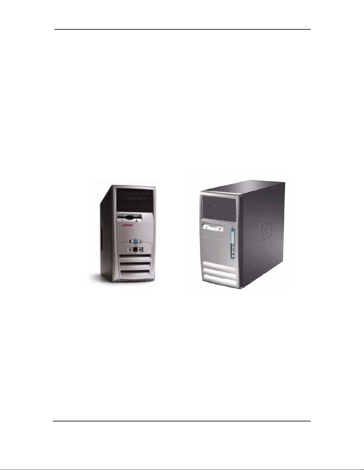
The Compaq D315 and HP d325 personal computers (Figure 2-1) deliver outstanding
manageability, serviceability, and compatibility for enterprise environments. Based on the AMD
Athlon XP processor and an NVidia NForce Chipset, these systems emphasize performance along
with industry compatibility. These models feature an architecture incorporating the PCI bus. All
models are easily upgradeable and expandable to keep pace with the needs of the office enterprise.
Compaq D315
hp d325
Figure 2-1. Compaq D315 and hp d325 Personal Computers
This chapter includes the following topics:
♦ Features and options (2.2) page 2-2
♦ Mechanical design (2.3) page 2-4
♦ System architecture (2.4) page 2-8
♦ Specifications (2.5) page 2-14
Compaq D315 and hp d325 Personal Computers
Featuring the AMD Athlon XP Processor
Second Edition - March 2003
2-1
Page 28

Chapter 2 System Overview
2.2 FEATURES AND OPTIONS
This section describes the standard features and available options.
2.2.1 STANDARD FEATURES
The following standard features are included on all models:
♦ AMD Athlon XP processor
♦ Three full-height, full-length PCI slots
♦ One AGP slot
♦ 3.5 inch, 1.44-MB diskette drive
♦ IDE controller w/UATA/100 mode support
♦ 5 drive bays (two internal 3.5”, two internal 5.25”, one 3.5” diskette drive)
♦ Hard drive fault prediction
♦ Communications interfaces including:
• One serial interface
• One parallel interface
• One network interface
• Six USB interfaces
♦ Plug ’n Play compatible (with ESCD support)
♦ Intelligent Manageability support
♦ Energy Star compliant
♦ Security features including:
• Flash ROM Boot Block
• Diskette drive disable, boot disable, write protect
• Power-on password
• Administrator password
• Serial/parallel port disable
♦ PS/2 Compaq Easy-Access keyboard w/Windows support
♦ PS/2 Compaq Scroll Mouse
♦ 220-watt Power Supply
♦ Available with Windows XP Home, XP Professional, or Mandrake Linux 8.2
Table 2-1 lists the differences between the Compaq D315 and hp d325 models.
Table 2-1. Feature Difference Matrix
Feature Difference Matrix
Feature Compaq D315 hp d325
DIMM type support (max) PC2100 DDR PC2700 DDR
Standard graphics controller Integrated GeForce2 MX Integrated GeForce 4 MX
AGP level of support 4X 8X
USB level of support 1.1 2.0
Multibay support? No Yes
Hood Sense/Hood Lock function? No Yes
Compaq D315 and hp d325 Personal Computers
2-2
Featuring the AMD Athlon XP Processor
Second Edition – March 2003
Table 2-1.
Page 29

Technical Reference Guide
2.2.2 OPTIONS
The following items are available as options for all models and may be included in the standard
configuration of some models:
♦ System Memory:
Model D315: PC2100 64-MB DDR DIMM (unbuffered, non-ECC)
PC2100 128-MB DDR DIMM (unbuffered, non-ECC)
PC2100 256-MB DDR DIMM (unbuffered, non-ECC)
PC2100 512-MB DDR DIMM (unbuffered, non-ECC)
Model D325: PC2700 64-MB DDR DIMM (unbuffered, non-ECC)
PC2700 128-MB DDR DIMM (unbuffered, non-ECC)
PC2700 256-MB DDR DIMM (unbuffered, non-ECC)
PC2700 512-MB DDR DIMM (unbuffered, non-ECC)
♦ Hard drives/controllers: 20-, 40-, 60, or 80-GB UATA/100 hard drive
32-GB Wide Ultra3 SCSI hard drive
♦ Removeable media drives: 16x/10x/40x CD-RW drive
10x/40x Max DVD-ROM drive
LS-120 Super Disk drive
PCI DXR DVD Decoder kit
♦ Graphics Monitors: Compaq P700 17” CRT
Compaq P900 19” CRT
Compaq P1100 21” CRT
Compaq TFT5010 15” Flat Panel
Compaq TFT8020 18” Flat Panel
Compaq D315 and hp d325 Personal Computers
Featuring the AMD Athlon XP Processor
Second Edition - March 2003
2-3
Page 30
Chapter 2 System Overview
2.3 MECHANICAL DESIGN
The following subsections describe the mechanical (physical) aspects of the Compaq D315 PC
and the HP Business PC d325 models.
CAUTION: Voltages are present within the system unit whenever the unit is plugged
into a live AC outlet, regardless of the system's “Power On” condition. Always
!
disconnect the power cable from the power outlet and/or from the system unit
before handling the system unit in any way.
NOTE: The following information is intended primarily for identification purposes
only. Before servicing these systems refer to the applicable Service Reference
Guide. Service personnel should review training materials also available on
these products.
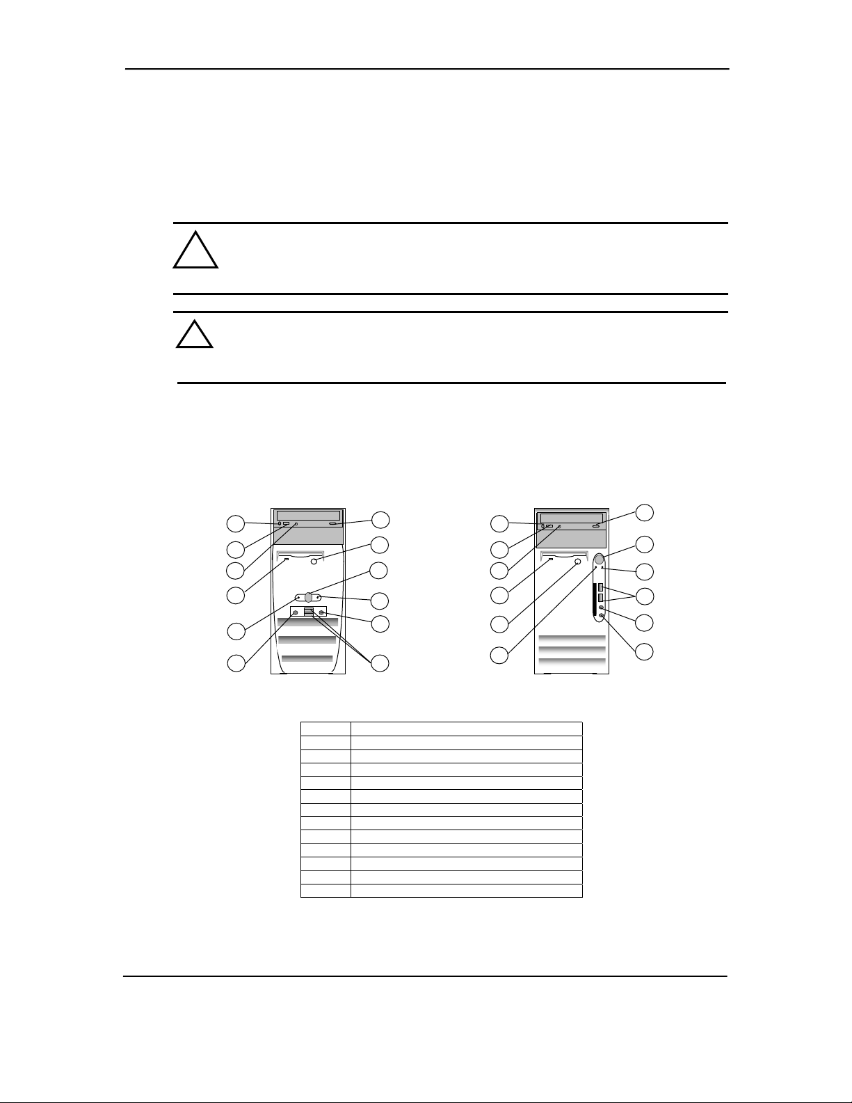
2.3.1 CABINET LAYOUTS
2.3.1.1 Front Views
1
2
3
5
10
8
Compaq D315 hp d325
Item Description
1 CD-ROM drive headphone jack
2 CD-ROM drive volume control
3 CD-ROM drive activity LED
4 CD-ROM drive open/close button
5 1.44-MB diskette drive activity LED
6 1.44-MB diskette drive eject button
7 Microphone In Jack
8 Headphone Out Jack
9 Universal Serial Bus Connectors (2)
10 Power LED
11 Power Button
12 Hard Drive Activity LED
11
12
4
9
7
8
11
12
4
6
7
9
10
1
2
3
5
6
Figure 2-2. Cabinet Layout, Front Views
Compaq D315 and hp d325 Personal Computers
2-4
Featuring the AMD Athlon XP Processor
Second Edition – March 2003
Page 31
Technical Reference Guide
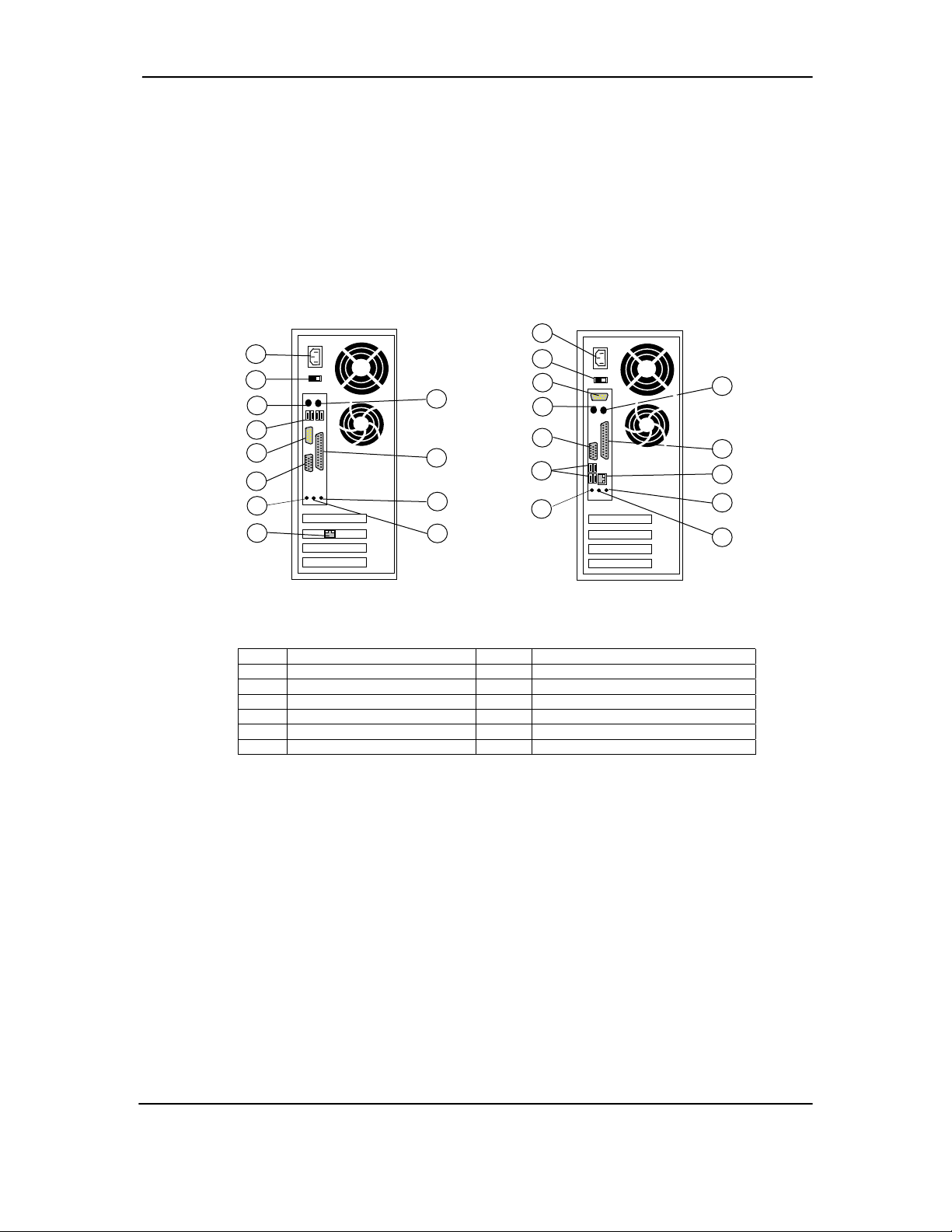
2.3.1.2 Rear Views
Figure 2-4 shows the rear view of the Compaq D315 and HP d325 systems.
12
10
11
2
1
4
3
5
7
6
8
9
Compaq D315
Item Description
1 AC voltage switch 7 VGA monitor connector
2 AC power connector 8 Audio microphone in jack
3 Mouse connector 9 Audio line input jack
4 Keyboard connector 10 Audio line output jack
5 Serial connector 11 Network interface connector
6 Parallel connector 12 USB ports (4)
Item Description
12
2
1
5
4
7
9
11
10
3
6
9
hp d325
Figure 2-3. Cabinet Layout, Rear Views
Compaq D315 and hp d325 Personal Computers
Featuring the AMD Athlon XP Processor
Second Edition - March 2003
2-5
Page 32
Chapter 2 System Overview
(
y)
2.3.2 CHASSIS LAYOUT
This section describes the internal layout of the chassis. For detailed information on servicing the
chassis refer to the multimedia training and/or the Service Reference Guide for these systems.
Figure 2-4 shows the layout for the Compaq D315 or hp d325 personal computers.
Power Supply
Processor/Heat Sink/Fan
Assembly
Chassis Fan
AGP Slot
NIC Card [1] in PCI Slot 1
PCI Slot 2
PCI Slot 3
NOTES/LEGEND:
[1] If present.
D315 model (board mounted horizontally)
d325 model
Back
board mounted veriticall
Externally Accessible
Drive Bays
Internal
Drive Bays
Front
Front Panel
Audio/USB
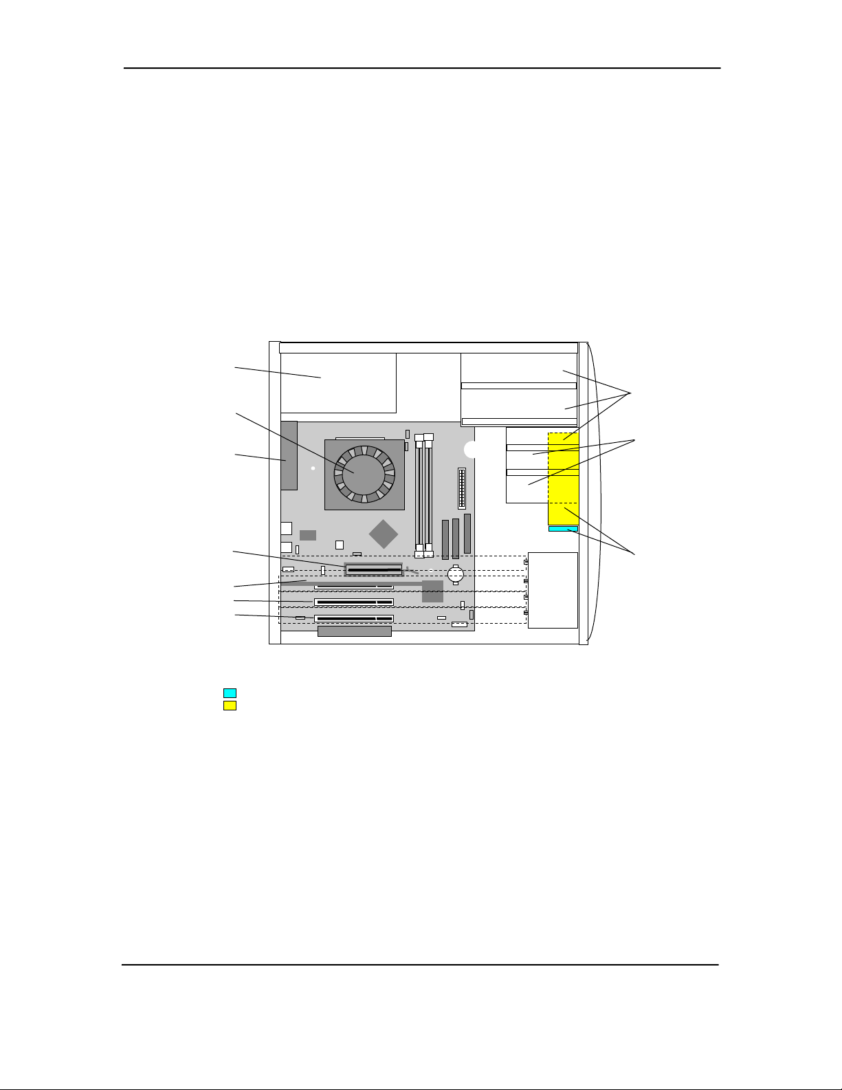
Figure 2-4. Chassis Layout, Left Side View
Compaq D315 and hp d325 Personal Computers
2-6
Featuring the AMD Athlon XP Processor
Second Edition – March 2003
Page 33

Technical Reference Guide
2.3.3 BOARD LAYOUTS
Figure 2-5 shows the system boards.
2
1
3
5
4
6
9
8 7
1
4
3
37
8 5
6
29
10
2
28
27
26
25
24
23 22 21
20
19
D315 d325
11
12
13
14
15
16
17
18
27
26
10
36
23
24
34
33 32 25
18
20
19
31
Item Description
1 PCI slots 20 Primary ATA connector
2 Front panel audio connector 21 Battery
3 Chassis fan connector 22 CMOS clear jumper
4 Audio jacks: Mic in (top), line in, line out 23 Front panel USB connector
5 VGA connector 24 Front panel power switch / LED connector
6 Parallel port connector 25 Password clear jumper
7 Serial port connector 26 AGP slot
8 USB ports [2] 27 Safe mode jumper
9 Top: Mouse port; bottom: keyboard port 28 PCI bus expansion connector [1]
10 CD audio connector 29 Auxiliary audio connector
11 Processor power 30 Serial port (COM1) conenc/tor
12 Processor socket 31 MultiBay connector
13 Processor fan connector 32 Hood sense connector
14 Fan ground control 33 Hood lock connector
15 Fan power control 34 BIOS boot block connector
16 DIMM sockets 35 Fan CMD connector
17 Secondary ATA connector 36 Speaker audio connector
18 Power supply connector 37 NIC connector (top), USB ports (2) bottom
19 Diskette drive connector -- --
NOTE8:
[1] Not used in this system.
[2] D315 board, 4 stack; d325 board, 2 stack
Item Description
9
11
29
30
12
13
16
21
17
Figure 2-5. System Board Layouts
Compaq D315 and hp d325 Personal Computers
Second Edition - March 2003
2-7
Featuring the AMD Athlon XP Processor
Page 34

Chapter 2 System Overview
2.4 SYSTEM ARCHITECTURE
The Compaq D315 and HP d325 feature an architecture based on the AMD Athlon XP processor
and an NVidia NForce chipset (Figure 2-6).
The AMD Athlon XP processor features an x86-class CPU that uses a highly-pipelined
architecture to process a high volume of data per clock cycle to provide exceptional performance
in handling audio, video, and image files. Operating at speeds up to 2.13 GHz, the Athlon XP
processor is optimized for the Microsoft Windows XP operating system.
The D315 model uses a Nvidia NForce 220 chipset while the d325 model uses the NForce2 420
chipset. Both chipsets include the following functions and features:
♦ Athon XP processor support
♦ Integrated Graphics Processor (IGP) providing:
• Integrated GeForce MX-class graphics controller
• AGP interface support for graphics upgrade
• SDRAM controller supporting two DDR DIMMs
♦ Media & Communication Processor (MCP) providing:
• Two IDE controllers supporting up to four ATA100 storage devices
• Six USB ports
• AC link interface servicing the audio controller
• PCI bus controller supporting up to three 32-bit 33-MHz PCI expansion devices
• LPC bus interface serving the BIOS ROM and super I/O component
Table 2-1 lists the architectural differences between the D315 and d325 models:
Table 2-2. Feature Difference Matrix
Table 2-2.
Architectural Difference Matrix
Feature Compaq D315 hp d325
Chipset type:
North Bridge Component
South Bridge Component
FSB speed (max) 266 MHz 333 MHz
DIMM type support (max) PC2100 DDR PC2700 DDR
Standard graphics controller Integrated GeForce2 MX Integrated GeForce 4 MX
AGP level of support (max) 4X 8X
USB level of support (max) 1.1 2.0
Network Interface Controller Separate PCI card Integrated
Multibay support? No Yes
Hood Sense/Hood Lock function? No Yes
NForce 220
IGP-64
MCP
NForce2 420
IGP-128
MCP-2
An STC LPC47B367 Super I/O Controller provides legacy PS/2 keyboard and mouse interfaces,
serial and parallel interfaces, and diskette drive interface functions.
Compaq D315 and hp d325 Personal Computers
2-8
Featuring the AMD Athlon XP Processor
Second Edition – March 2003
Page 35
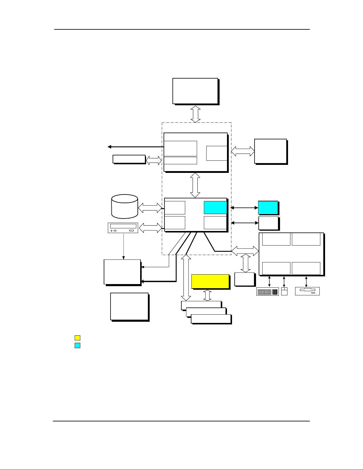
Technical Reference Guide
Athlon XP
Processor
NForce Chipset
Monitor
RGB
AGP Slot
GeForce
MX Graphics
AGP I/F
FSB
North Bridge
SDRAM
Cntlr.
Memory
Bus
DDR
SDRAM
ATA100
Hard Drive
IDE Bus
IDE Bus
Pri.
Sec.
Pri. IDE
Cntlr.
Sec. IDE
Cntlr.
CD
Audio
Audio
Subsystem
Beep
Audio
AC’97
Link Bus
Hyper
Transport
Link
Bus
NIC
South
Bridge
Cntlr.
USB
Cntlrs.
33-MHz 32-Bit
PCI Bus
10/100 NIC
PCI Card
TX/RX
Data
TX/RX
Data
LPC
Bus
BIOS
ROM
NIC
PHY
USB
I/F (6)
Serial
I/F
LPC47B367 I/O Controller
Keyboard/
Mouse I/F
Parallel
Diskette
I/F
I/F
D315 models only
d325 models only
Power
Supply
PCI Slot 1
PCI Slot 2
PCI Slot 3
Figure 2-6. System Architecture, Block Diagram
Compaq D315 and hp d325 Personal Computers
Featuring the AMD Athlon XP Processor
Second Edition - March 2003
2-9
Page 36

Chapter 2 System Overview
2.4.1 AMD ATHLON XP PROCESSOR
The systems covered in this guide feature the AMD Athlon XP processor. This processor is
compatible with software written for most x86-type microprocessors including the AMD Duron
and Intel Pentium-type processors and includes the following features:
♦ QuantiSpeed
♦ 128-KB L1 and 256-KB L2 full-speed caches
♦ 3DNow!
♦ 0.13 micron copper process technology
The Athlon XP processor uses a nine-stage, superscalar pipelined CPU core to process more
instructions in a given clock cycle than other x86-type processors. Optimized for the Windows XP
operating systems, the Athlon XP processor is also compatible with all earlier Windows operating
systems (Windows 2000, ME, and 98). These systems use the Socket-A method of processor
mounting as shown in Figure 2-7.
Heat Sink / Fan Assembly
Heat Sink Retaining Clip
(Shown in unlock position)
TM
architecture
TM
professional technology (full SSE compatibility)
Lock/Unlock
Handle
Fan Power Cable
OPGA2 Package
Socket A
Figure 2-7. Heat Sink, Processor, and Socket Assemblies
NOTE: Heat sink types are not interchangeable. Also, these systems support processors
using the OPGA2 package only.
Compaq D315 and hp d325 Personal Computers
2-10
Featuring the AMD Athlon XP Processor
Second Edition – March 2003
Page 37

Technical Reference Guide
2.4.2 CHIPSET
The D315 model uses a NVidia NForce 220 chipset while the D325 model uses the NVidia
NForce2 chipset. Table 2-3 provides a comparison of the two chipset types.
Table 2-3. Chipset Functions
Table 2-3. NVidia Chipset Comparison
Component NForce 220 NForce 2 420
North Bridge
FSB speed (max)
Memory Bandwidth (max)
Graphics Processing Unit
AGP Interface (max)
South Bridge
PCI bus I/F
LPC bus I/F
Two IDE UATA/100 controllers
AC Link controller
IRQ controller
Power management logic
Two USB 1.1 controllers
One USB 2.0 controller
Unless otherwise indicated, all functions are common to both chipsets.
NOTE:
IGP-64
266-MHz
64-bit
GeForce2 MX
4X
MCP
Yes
Yes
Yes
Yes
Yes
Yes
Yes
No
2.4.3 SUPPORT COMPONENTS
Input/output functions not provided by the chipset are handled by other support components.
Some of these components also provide “housekeeping” and various other functions as well.
Table 2-4 shows the functions provided by the support components.
IGP-128
333-MHz
128-bit
GeForce4 MX
8X
MCP-2
Yes
Yes
Yes
Yes
Yes
Yes
Yes
Yes
Table 2-4. Support Component Functions
Table 2-4.
Support Component Functions
Component Name Function
LPC47B367 I/O Controller Keyboard and pointing device I/F
AD1885 (D315) or
AD1981 (d325) Audio Codec
Diskette I/F
Serial I/F (1)
Parallel I/F (1)
AGP, PCI reset generation
Interrupt (IRQ) serializer
Power button logic
GPIO ports
Audio mixer
Digital-to-analog converter
Analog-to-digital converter
Analog I/O
6-channel audio support (AD1981 only)
Compaq D315 and hp d325 Personal Computers
Second Edition - March 2003
2-11
Featuring the AMD Athlon XP Processor
Page 38

Chapter 2 System Overview
2.4.4 SYSTEM MEMORY
These systems use the NVidia IGP component that supports DDR SDRAM. The system board
provides two sockets that accept industry-standard unbuffered DDR DIMMs.
The D315 system uses the IGP-64 controller that supports 64-bit PC2100 DDR memory and a
maximum of 1 gigabyte of memory.
The d325 system uses the IGP-128 controller supporting 128-bit (when two DIMMs are installed)
PC2700 DDR memory and a maximum of 2 gigabytes of memory.
2.4.5 MASS STORAGE
All models include a 3.5 inch 1.44-MB diskette drive installed as drive A. Most models also
include a CD-ROM and a 20- to 80-GB hard drive. Standard hard drives feature Drive Protection
System (DPS) support. All systems provide two (one primary, one secondary) PCI bus-mastering
Enhanced IDE (EIDE) controllers integrated into the chipset. Each controller provides
UATA/100 support for two drives for a total of four IDE devices, although the form factor will
determine the actual number of drive spaces available.
2.4.6 SERIAL AND PARALLEL INTERFACES
This system includes one serial port and a parallel port accessible at the rear of the chassis. The
serial interface is RS-232-C/16550-compatible and supports standard baud rates up to 115,200 as
well as two high-speed baud rates of 230K and 460K, and utilizes a DB-9 connector. The parallel
interface is Enhanced Parallel Port (EPP1.9) and Enhanced Capability Port (ECP) compatible, and
supports bi-directional data transfers through a DB-25 connector.
2.4.7 UNIVERSAL SERIAL BUS INTERFACE
The Universal Serial Bus (USB) interface supports hot plugging/unplugging (Plug ’n Play)
functionality for six USB ports. Two ports are accessible at the front of the unit and four ports are
available at the rear of the chassis. The D315 model provides USB 1.1 support while the d325
model provides 2.0 support.
Compaq D315 and hp d325 Personal Computers
2-12
Featuring the AMD Athlon XP Processor
Second Edition – March 2003
Page 39

Technical Reference Guide
2.4.8 NETWORK INTERFACE CONTROLLER
All models feature a Network Interface Controller (NIC). The D315 model includes either a
Accton 10/100 NIC featuring Wake-On-LAN or an Intel 10/100 NIC PCI card featuring WOL
and AOL, depending on configuration. The d325 model features a 3Com NIC integrated on the
system board.
2.4.9 GRAPHICS SUBSYSTEM
The IGP component provides AGP interface support as well as including a GeForce MX-class
graphics processing unit. The system may be upgraded adding a separate AGP card to replace the
integrated graphic controller.
Table 2-5 lists the key specifications of the standard graphics subsystems employed in these
systems:
Table 2-5. Standard Graphics Subsystem Comparison
Bus Type AGP 4X AGP 8X
Graphics processing unit GeForce 2 MX GeForce 4 MX
DAC Speed 300 MHz 300 MHz
Max. 2D Res.
Software Compatibility S3TC
Table 2-5.
Standard Graphics Support Comparison
D315 d325
1900 x 1200 1900 x 1200
DCI/DirectX,
Direct Draw,
MPEG 1/2,
S3TC
DCI/DirectX,
Direct Draw,
MPEG 1/2,
Compaq D315 and hp d325 Personal Computers
Featuring the AMD Athlon XP Processor
Second Edition - March 2003
2-13
Page 40

Chapter 2 System Overview
2.4.10 AUDIO SUBSYSTEM
This system uses the integrated AC97 audio controller of the chipset and the Analog Devices
AD1885 (D315 models) or AD1981 (d325 models) codec. These systems include microphone and
line inputs and headphone and line outputs. The system includes a 3-watt output amplifier driving
an internal speaker, and the headphone and microphone jacks are duplicated on both the front
panel and the rear chassis panel.
2.5 SPECIFICATIONS
This section includes the environmental, electrical, and physical specifications for the HewlettPackard Personal Computers. Where provided, metric statistics are given in parenthesis. All
specifications are subject to change without notice.
Table 2-6. Environmental Specifications
Environmental Specifications (Factory Configuration)
Parameter Operating Nonoperating
Ambient Air Temperature 50o to 95o F (10o to 35o C, max. rate
Shock (w/o damage) 5 Gs [1] 20 Gs [1]
Vibration
Humidity
Maximum Altitude 10,000 ft (3048 m) [2] 30,000 ft (9144 m) [2]
NOTE:
[1] Peak input acceleration during an 11 ms half-sine shock pulse.
[2] Maximum rate of change: 1500 ft/min.
Table 2-6.
o
-24
of change <
0.000215 G2/Hz, 10-300 Hz 0.0005 G2/Hz, 10-500 Hz
10-90% Rh @ 28o C max.
wet bulb temperature
10°C/Hr)
to 140o F (-30o to 60o C, max. rate
of change <
5-95% Rh @ 38.7o C max.
wet bulb temperature
20°C/Hr )
Table 2-7. Electrical Specifications
Parameter U.S. International
Input Line Voltage:
Nominal:
Maximum:
Input Line Frequency Range:
Nominal:
Maximum:
Power Supply:
Maximum Continuous Power
Maximum Line Current Draw
Compaq D315 and hp d325 Personal Computers
2-14
Featuring the AMD Athlon XP Processor
Second Edition – March 2003
Table 2-7.
Electrical Specifications
100 - 127 VAC
90 - 132 VAC
50 - 60 Hz
47 - 63 Hz
235 watts
3.6 A @ 100 VAC
3.6 A @ 200 VAC
200 - 240 VAC
180 - 264 VAC
50 - 60 Hz
47 - 63 Hz
235 watts
Page 41

Technical Reference Guide
Table 2-8. Physical Specifications
Table 2-8.
Physical Specifications
Height 14.50 in (36.83 cm)
Width 6.88 in (17.48 cm)
Depth
Weight (nom.) [1]
Maximum
Supported Weight [2]
NOTES:
[1] System weight may vary depending on installed drives/peripherals.
[2] Assumes reasonable article(s) such as a display monitor and/or another system unit.
16.55 in (42.04 cm)
23.8 lb (10.92 kg)
100 lb (45.50 kg)
Table 2-9. Diskette Drive Specifications
Table 2-9.
Diskette Drive Specifications
(Compaq SP# 278644-001)
Parameter Measurement
Media Type 3.5 in 1.44 MB/720 KB diskette
Height 1/3 bay (1 in)
Bytes per Sector 512
Sectors per Track:
High Density
Low Density
Tracks per Side:
High Density
Low Density
Read/Write Heads 2
Average Access Time:
Track-to-Track (high/low)
Average (high/low)
Settling Time
Latency Average
18
9
80
80
3 ms/6 ms
94 ms/169ms
15 ms
100 ms
Compaq D315 and hp d325 Personal Computers
Featuring the AMD Athlon XP Processor
Second Edition - March 2003
2-15
Page 42

Chapter 2 System Overview
Table 2-10. Optical Drive Specifications
Parameter 48x CD-ROM 16/10/40x CD-RW Drive
Part number 232320-001 281749-001
Interface Type IDE IDE
Media Type (reading)
Media Type (writing) N/a CD-R, CD-RW
Transfer Rate (Reads) 4.8 Kb/s (max sustained) CD-ROM, 4.8 Kb/s;
Transfer Rate (Writes): N/a CD-R, 2.4 Kbps (sustained);
Capacity:
Mode 1, 12 cm
Mode 2, 12 cm
8 cm
Center Hole Diameter 15 mm 15 mm
Disc Diameter 8/12 cm 8/12 cm
Disc Thickness 1.2 mm 1.2 mm
Track Pitch 1.6 um 1.6 um
Laser
Beam Divergence
Output Power
Type
Wave Length
Average Access Time:
Random
Full Stroke
Audio Output Level 0.7 Vrms 0.7 Vrms
Cache Buffer 128 KB 128 KB
Table 2-10.
Optical Drive Specifications
Mode 1,2, Mixed Mode, CD-DA,
Photo CD, Cdi, CD-XA
540 MB
650 MB
180 MB
53.5 +/- 1.5 °
53.6
0.14 mW
GaAs
790 +/- 25 nm
<100 ms
<150 ms
Mode 1,2, Mixed Mode, CD-DA,
Photo CD, Cdi, CD-XA
CD-ROM/CD-R, 1.5-6 Kb/s
CD-RW, 1.5 Kbps (sustained);
650 MB @ 12 cm
180 cm
53.5 + 1.5°
53.6 0.14 mW
GaAs
790 +/- 25 nm
<120 ms
<200 ms
Table 2-11. Hard Drive Specifications
Hard Drive Specifications
Parameter 20.0 GB 20.0 GB 40.0 GB 40.0 GB
Part Number 249408-001 260671-001 236421-001 286692-001
Drive Size 3.5” 3.5” 3.5” 3.5”
Interface UATA/100 UATA/100 UATA/100 UATA/100
Transfer Rate 100 MBps 100 MBps 100 MBps 100 MBps
Drive Protection System Support? Yes Yes Yes Yes
Typical Seek Time (w/settling) [1]
Single Track
Average
Full Stroke
Disk Format (logical blocks) 39,102,336 39,102,336 39,102,336 78,165,360
Rotation Speed 5400 RPM 7200 RPM 5400 RPM 7200 RPM
Drive Fault Prediction SMART III SMART III SMART III SMART III
NOTE:
Actual times may vary depending on specific drive installed.
Compaq D315 and hp d325 Personal Computers
2-16
Featuring the AMD Athlon XP Processor
Second Edition – March 2003
Table 2-11.
2.0 ms
12.8 ms
28.5 ms
1.2 ms
8.0 ms
18 ms
1.5 ms
10.5 ms
23 ms
1.2 ms
8.0 ms
18 ms
Page 43
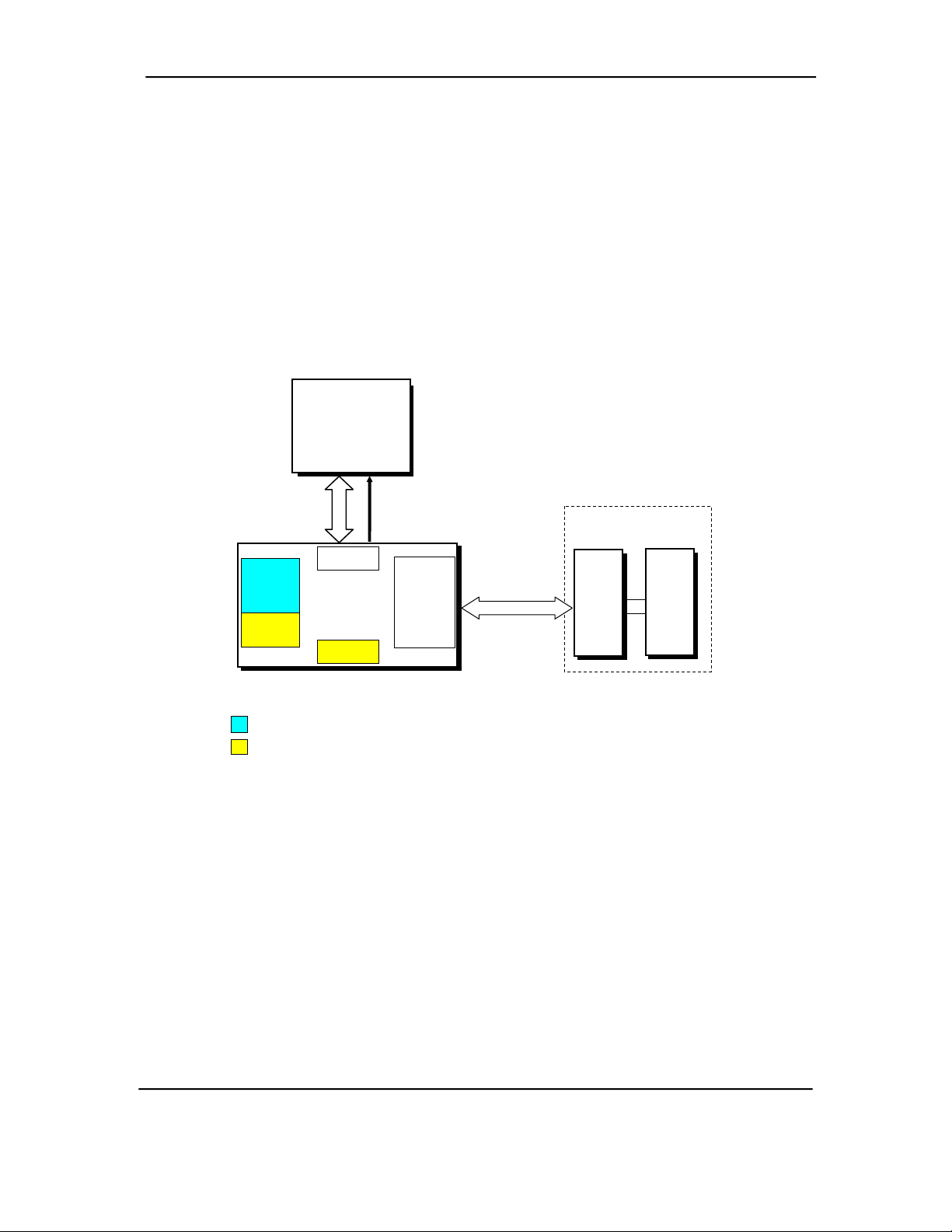
Technical Reference Guide
Chapter 3 PROCESSOR/ MEMORY SUBSYSTEM
3. Chapter 3 PROCESSOR/MEMORY SUBSYSTEM
3.1 INTRODUCTION
This chapter describes the processor/memory subsystem. These systems feature the AMD Athlon XP
processor and an NVidia NForce chipset (Figure 3-1).
[1] D315, 64-bit;
d325, 128-bit (max)
Athlon XP
Processor
64-Bit FSB
GPU
AGP
I/F
Covered in chapter 6.
Covered in chapter 4
FSB I/F
IGP
HT I/F
Cntl
Memory
Cntlr.
Memory
Bus [1]
System Memory
XMM1
DIMM
In
Socket
XMM2
DIMM
Socket
Figure 3–1. Processor/Memory Subsystem Architecture
This chapter includes the following topics:
♦ AMD Athlon XP processor (3.2) page 3-2
♦ Memory subsystem (3.3) page 3-5
♦ Subsystem configuration (3.4) page 3-8
Compaq D315 and hp d325 Personal Computers
3-1
Featuring the AMD Athlon XP Processor
Second Edition - April 2003
Page 44

Chapter 3 Processor/Memory Subsystem
3.2 ATHLON XP PROCESSOR
This system features an AMD Athlon XP processor in a Socket 462-compatible package mounted
with a passive heat sink. The mounting socket allows the processor to be easily changed for
servicing and/or upgrading.
3.2.1 PROCESSOR OVERVIEW
The AMD Athlon XP processor represents the latest development of AMD processors that takes
advantage of the Windows XP operating system. The Athlon XP processor is well-suited for
demanding applications involving digital photo manipulation, video editing, audio and video
streaming over the internet, 3D modeling, and commercial desktop publishing.
Key features of the Athlon XP processor include:
♦ Superpipelined, superscalar technology – A nine-stage pipeline for increased processing
frequencies.
♦ Multple x86 instruction decoders for parallel processing
♦ Hardware data prefetch
♦ Advanced Translation Look-Aside Buffer for data and instruction addresses
♦ Large full-speed 384-KB cache – 128-KB L1 cache and 256-KB L2 cache
♦ Enhanced Floating Point Processor - Executes all x87 (math co-processor), MMX, SSE, and
3DNow! instructions.
♦ Advanced dynamic branch prediction
The Athlon XP processor is backward-compatible with software written for most x86-type
processors such as the AMD Athlon 4, AMD Duron, and Intel Pentium processors. The Athlon
XP processor supports applications using MMX, SSE, and 3DNow! instructions.
Manufactured using 0.13 micron technology, the Athlon XP processor’s uses a deeply-pipelined,
superscalar architecture that uses three x86 instruction decoders that each feed an execution
engine. Parallel execution engines provide a 3-instruction-per-clock cycle ability that is
unmatched by other x86 processors. In addition, the floating pointing unit features QuantiSpeed
architecture that uses three execution units that work in parallel to process as many as four 32-bit
floating point results per cycle.
Compaq D315 and hp d325 Personal Computers
3-2
Featuring the AMD Athlon XP Processor
Second Edition - April 2003
Page 45

Technical Reference Guide
Figure 3-2 illustrates the internal architecture of the Athlon XP processor.
Branch
Prediction
Integer
ALUs 1-3
Athlon XP Processor
3-Way Instruction
Decoders
CPU
FPU
128-bit
Integer
FPU
FSB
I/F
128-K
L1
Cache
256-K
L2
Cache
Athlon XP Type Core Speed Voltage Max. Current Max. Power
Model 6 1500+ 1333 MHz 1.75 VDC 34.3 A 60.0 W
Model 6 1600+ 1400 MHz 1.75 VDC 35.9 A 62.8 W
Model 6 1700+ 1467 MHz 1.75 VDC 36.6 A 64.0 W
Model 8 1700+ 1467 MHz 1.50 VDC 32.9 A 49.4 W
Model 6 1800+ 1533 MHz 1.75 VDC 37.7 A 66.0 W
Model 8 1800+ 1533 MHz 1.50 VDC 34.0 A 51.0 W
Model 6 1900+ 1600 MHz 1.75 VDC 38.9 A 68.0 W
Model 8 1900+ 1600 MHz 1.50 VDC 35.0 A 52.2 W
Model 6 2000+ 1667 MHz 1.75 VDC 40.0 A 70.0 W
Model 8 2000+ 1667 MHz
“
“
Model 6 2100+ 1733 MHz 1.75 VDC 41.1 A 72.0 W
Model 8 2100+ 1733 MHz 1.60 VDC 38.8 A 61.1 W
Model 8 2200+ 1800 MHz
“
Model 8 2400+ 2000 MHz 1.65 VDC 41.4 A 68.3 W
Model 8 2600+ 2133 MHz
2083 MHz
Model 8 2800+ 2083 MHz 1.65 VDC 41.4 A 68.3 W
Model 8 3000+ 2167 MHz 1.65 VDC 45.0 A 74.3 W
1.60 VDC
1.65 VDC
1.60 VDC
1.60 VDC
“
1.65 VDC
“
37.7 A
36.5 A
38.3 A
41.2 A
39.3 A
41.4 A
“
60.3 W
60.3 W
61.3 W
67.9 W
62.8 W
68.3 W
“
Figure 3–2. AMD Athlon XP Processor Internal Architecture and Key Statistics.
The Athlon XP processor uses 0.13 micron technology that yields lower power requirements for a
given processing speed. The system board supports the unit types listed in Figure 3-2.
The Athlon XP processor uses a 133-MHz (on D315 systems) or 166-MHz (on d325 systems)
clock signal for the front side bus. Data transfers are qualified on the both the rising and falling
edge of the clock cycle, effectively doubling the data throughput rate to 266- and 333-MHz.
Compaq D315 and hp d325 Personal Computers
3-3
Featuring the AMD Athlon XP Processor
Second Edition - April 2003
Page 46

Chapter 3 Processor/Memory Subsystem
The AMD Athlon XP processor is compatible with software written for Athlon 4, Duron, and
most other x86 processors, but will require the latest versions of operating system software to take
advantage of the specific features and functions.
3.2.2 PROCESSOR UPGRADING
This system uses the Socket A mounting socket. A replacement processor must use the same type
heat sink (passive or fan cooled) as the original to ensure proper cooling.
CAUTION: The D315 model supports processor speeds up to 2.0 gigahertz. The d325
!
model supports processor speeds up to 2.3 GHz. Using a processor that exceeds a
particular model’s capability may result in equipment failure and/or damage.
NOTE: These systems ship with Athlon XP processors but do support Duron processors
as well.
The heat sink is specially designed provide maximum heat transfer from the processor component.
CAUTION: Attachment of the heat sink to the processor is critical on these systems.
!
Improper attachment of the heat sink will likely result in a thermal condition.
Although the system is designed to detect thermal conditions and automatically shut
down, such a condition could still result in damage to the processor component. Refer to
the applicable Service Reference Guide for processor installation instructions.
Compaq D315 and hp d325 Personal Computers
3-4
Featuring the AMD Athlon XP Processor
Second Edition - April 2003
Page 47

Technical Reference Guide
3.3 MEMORY SUBSYSTEM
These systems provide two 184-pin DIMM sockets that accept DDR DIMMs. The D315 models
ship with PC2100 DIMMs while the d325 models ship with PC2700 DIMMs.
NOTE: The DDR SDRAM DIMM "PCxxxx" reference designates bus bandwidth (i.e.,
a PC2100 DIMM, operating at a 266-MHz effective speed, provides a throughput of
2100 MBps (8 bytes × 266 MHz)).
These systems support DIMMs with the following specifications:
♦ Unbuffered, non-ECC with SPD rev. 1.0
♦ CL (CAS latency) = 2, 2.5, or 3
♦ Single or double-sided
The following table lists the differences in DIMM support between the D315 and the D325
models:
DIMM Type (max speed) PC2100 (266-MHz) PC2700 (333-MHz)
Highest technology level supported 512 Mb 1024 Mb
Maximum amount supported 1 GB 2 GB
The SPD format as supported in this system (SPD rev. 1) is shown in Table 3-1. All DIMMs must
yield a value of 07h (indicating DDR memory) in SPD byte 02 (i.e., only DDR DIMMs are
supported in these systems).
The memory subsystem is controlled by the memory controller integrated into the IGP component
of the NVidia NForce chipset. The D315 model supports a 64-bit wide memory array with a
maximum capacity of up to 1-GB using 512-Mb memory technology. The d325 model provides
(with two DIMMs installed) a 128-bit wide memory array with a maximum capacity of 2 GB
using 1-Mb memory technology.
NOTE: Non-supported DIMMs will not be recognized by the BIOS during the boot
sequence and therefore not be used.
D315 d325
Compaq D315 and hp d325 Personal Computers
3-5
Featuring the AMD Athlon XP Processor
Second Edition - April 2003
Page 48

Chapter 3 Processor/Memory Subsystem
The SPD address map is shown below.
Table 3–1. SPD Address Map (SDRAM DIMM)
SPD Address Map (SDRAM DIMM)
Byte Description Notes Byte Description Notes
0 No. of Bytes Written Into EEPROM [1] 25 Min. CLK Cycle @ CL X-2 [7]
1 Total Bytes (#) In EEPROM [2] 26 Max. Acc. Frm CLK @ CL
2 Memory Type 27 Min. Row Prechge. Time [7]
3 No. of Row Addresses On DIMM [3] 28 Min. Row Active to Delay [7]
4 No. of Column Addresses On DIMM 29 Min. RAS to CAS Delay [7]
5 No. of Module Banks On DIMM 30, 31 Reserved
6, 7 Data Width of Module 32..61 Superset Data [7]
8 Voltage Interface Standard of DIMM 62 SPD Revision [7]
9 Cycletime @ Max CAS Latency (CL) [4] 63 Checksum Bytes 0-62
10 Access From Clock [4] 64-71 JEP-106E ID Code [8]
11 Config. Type (Parity, Nonparity, etc.) 72 DIMM OEM Location [8]
12 Refresh Rate/Type [4] [5] 73-90 OEM’s Part Number [8]
13 Width, Primary DRAM 91, 92 OEM’s Rev. Code [8]
14 Error Checking Data Width 93, 94 Manufacture Date [8]
15 Min. Clock Delay [6] 95-98 OEM’s Assembly S/N [8]
16 Burst Lengths Supported 99-125 OEM Specific Data [8]
17 No. of Banks For Each Mem. Device [4] 126 Intel frequency check
18 CAS Latencies Supported [4] 127 Reserved
19 CS# Latency [4] 128-131 Compaq header “CPQ1” [9]
20 Write Latency [4] 132 Header checksum [9]
21 DIMM Attributes 133-145 Unit serial number [9] [10]
22 Memory Device Attributes 146 DIMM ID [9] [11]
23 Min. CLK Cycle Time at CL X-1 [7] 147 Checksum [9]
24 Max. Acc. Time From CLK @ CL X-1 [7] Reserved [9]
NOTES:
[1] Programmed as 128 bytes by the DIMM OEM
[2] Must be programmed to 256 bytes.
[3] High order bit defines redundant addressing: if set (1), highest order RAS# address must be
re-sent as highest order CAS# address.
[4] Refer to memory manufacturer’s datasheet
[5] MSb is Self Refresh flag. If set (1), assembly supports self refresh.
[6] Back-to-back random column addresses.
[7] Field format proposed to JEDEC but not defined as standard at publication time.
[8] Field specified as optional by JEDEC but required by this system.
[9] Compaq usage. This system requires that the DIMM EEPROM have this
space available for reads/writes.
[10] Serial # in ASCII format (MSB is 133). Intended as backup identifier in case vender data is
invalid.
Can also be used to indicate s/n mismatch and flag system adminstrator of possible system
Tampering.
[11] Contains the socket # of the module (first module is “1”). Intended as backup identifier (refer to
note [10]).
Table 3-1.
[7]
X-2
Compaq D315 and hp d325 Personal Computers
3-6
Featuring the AMD Athlon XP Processor
Second Edition - April 2003
Page 49

Technical Reference Guide
Figure 3-3 shows the system memory map.
Host,
PCI, AGP Area
FFFF FFFFh
FFE0 0000h
FFDF FFFFh
FEC1 0000h
FEC0 FFFFh
FEC0 0000h
FEBF FFFFh
High BIOS Area
(2 MB)
PCI Memory
(18 MB)
APIC Config. Space
(64 KB)
PCI Memory
Expansion
(3060 MB)
4 GB
2000 0000h
1FFF FFFFh
[1]
Host, PCI,
ISA Area
0100 0000h
00FF FFFFh
0010 0000h
000F FFFFh
000E 0000h
000D FFFFh
DOS Compatibility
Area
000C 0000h
000B FFFFh
000A 0000h
0009 FFFFh
0008 0000h
0007 FFFFh
NOTE:
All locations in memory are cacheable. Base memory is always mapped to DRAM. The next 128 KB
fixed memory area can, through the north bridge, be mapped to DRAM or to PCI space. Graphics RAM
area is mapped to PCI or AGP locations.
[1] D315 model, 1 GB; d325, 2 GB
[2] Area typically less according to need and Setup configuration. Default area is E6100-FFFFFh.
0000 0000h
Host/PCI Memory
Expansion
(496 MB)
16 MB
Extended Memory
(15 MB)
1 MB
System BIOS Area
(128 KB max [2] )
Option ROM
(128 KB)
Graphics/SMRAM
RAM (128 KB)
640 KB
Fixed Mem. Area
(128 KB)
512 KB
Base Memory
(512 KB)
Figure 3–3. System Memory Map
Compaq D315 and hp d325 Personal Computers
3-7
Featuring the AMD Athlon XP Processor
Second Edition - April 2003
Page 50

Chapter 3 Processor/Memory Subsystem
This page is intentionally blank.
Compaq D315 and hp d325 Personal Computers
3-8
Featuring the AMD Athlon XP Processor
Second Edition - April 2003
Page 51

Technical Reference Guide
Chapter 4 SYSTEM SUPPORT
4. Chapter 4 SYSTEM SUPPORT
4.1 INTRODUCTION
This chapter covers subjects dealing with basic system architecture and covers the following
topics:
♦ PCI bus overview (4.2) page 4-2
♦ AGP bus overview (4.3) page 4-9
♦ System resources (4.4) page 4-13
♦ System clock distribution (4.5) page 4-20
♦ Real-time clock and configuration memory (4.6) page 4-21
♦ System management (4.7) page 4-23
♦ Register map and miscellaneous functions (4.8) page 4-29
This chapter covers functions provided by off-the-shelf chipsets and therefore describes only basic
aspects of these functions as well as information unique to the systems covered in this guide. For
detailed information on specific components, refer to the applicable manufacturer’s
documentation.
Compaq D315 and hp d325 Personal Computers
Second Edition - April 2003
4-1
Featuring the AMD Athlon XP Processor
Page 52
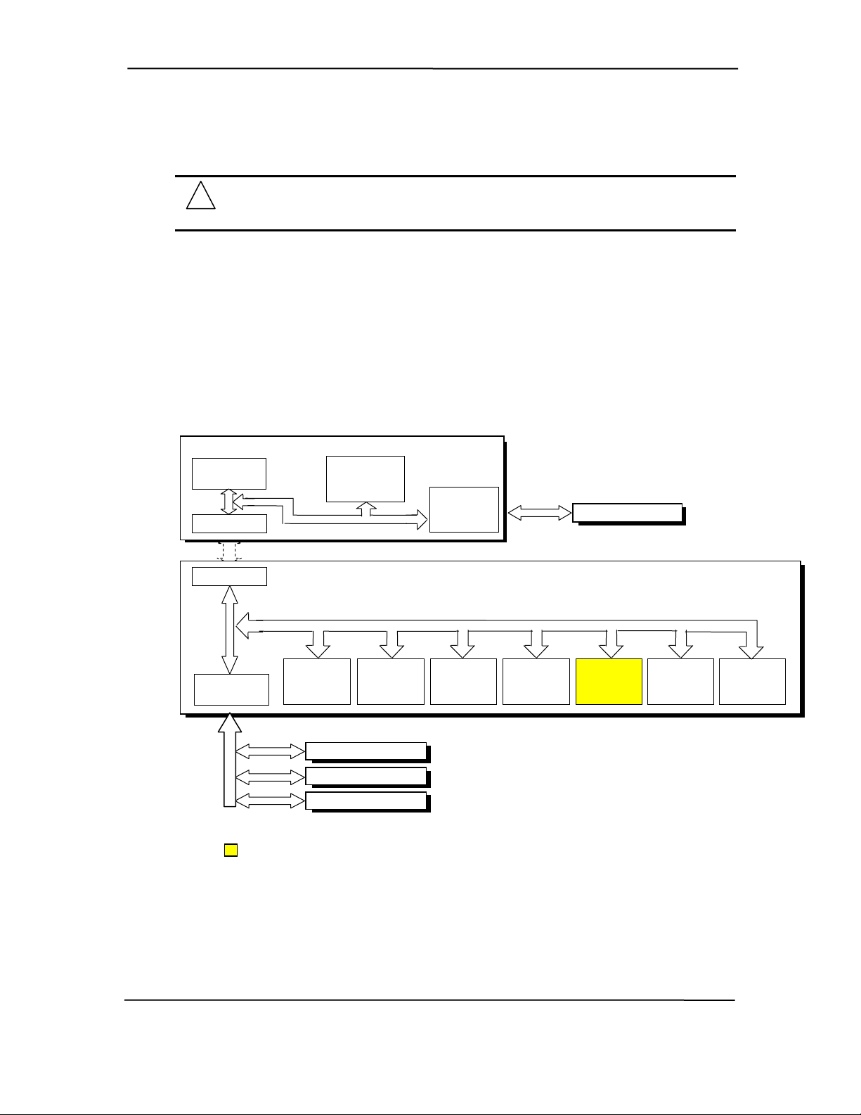
Chapter 4 System Support
4.2 PCI BUS OVERVIEW
NOTE: This section describes the PCI bus in general and highlights bus
implementation in this particular system. For detailed information regarding PCI bus
operation, refer to the PCI Local Bus Specification Revision 2.2.
These systems implement a 32-bit Peripheral Component Interconnect (PCI) bus (spec. 2.2)
operating at 33 MHz. The PCI bus handles address/data transfers through the identification of
devices and functions on the bus. A device is typically defined as a component or slot that resides
on the PCI bus (although some components such as the IGP and MCP or MCP-2 are organized as
multiple devices). A function is defined as the end source or target of the bus transaction. A
device may contain one or more functions.
In the standard configuration these systems use a hierarchy of three PCI buses (Figure 4-1). The
PCI bus #0 is internal to the chipset components and is not physically accessible. The AGP bus
that services the AGP slot is designated as PCI bus #1. All PCI slots reside on PCI bus #2.
Mem. Cntlr.
Function
HT Link I/F
HT Link I/F
PCI Bridge
Function
NOTE:
Not implemented in the D315 system.
Hyper Transfer Link Bus
PCI
Bus #2
IGP Component
PCI
Bus #0
Legacy
Function
PCI Connector 1
PCI Connector 2
PCI Connector 3
Integrated
Graphics
Controller
SMBus
Controller
Function
PCI Bus #0
AGP
Bridge
Function
MCP or MCP-2 Component
USB
Cntlr. A
Function
PCI Bus #1
(AGP Bus)
USB
Cntlr. b
Function
AGP Connector
Network
Interface
Function
AC97
Audio
Function
IDE
Controller
Function
Figure 4-1. PCI Bus Devices and Functions
Compaq D315 and hp d325 Personal Computers
4-2
Featuring the AMD Athlon XP Processor
Second Edition – April 2003
Page 53

Technical Reference Guide
4.2.1 PCI BUS TRANSACTIONS
The PCI bus consists of a 32-bit path (AD31-00 lines) that uses a multiplexed scheme for
handling both address and data transfers. A bus transaction consists of an address cycle and one
or more data cycles, with each cycle requiring a clock (PCICLK) cycle. High performance is
realized during burst modes in which a transaction with contiguous memory locations requires
that only one address cycle be conducted and subsequent data cycles are completed using autoincremented addressing. Four types of address cycles can take place on the PCI bus; I/O, memory,
configuration, and special. Address decoding is distributed (left up to each device on the PCI bus).
4.2.1.1 I/O and Memory Cycles
For I/O and memory cycles, a standard 32-bit address decode (AD31..0) for byte-level addressing
is handled by the appropriate PCI device. For memory addressing, PCI devices decode the
AD31..2 lines for dword-level addressing and check the AD1,0 lines for burst (linearincrementing) mode. In burst mode, subsequent data phases are conducted a dword at a time with
addressing assumed to increment accordingly (four bytes at a time).
4.2.1.2 Configuration Cycles
Devices on the PCI bus must comply with PCI protocol that allows configuration of that device by
software. In this system, configuration mechanism #1 (as described in the PCI Local Bus
specification Rev. 2.2) is employed. This method uses two 32-bit registers for initiating a
configuration cycle for accessing the configuration space of a PCI device. The configuration
address register (CONFIG_ADDRESS) at 0CF8h holds a value that specifies the PCI bus, PCI
device, and specific register to be accessed. The configuration data register (CONFIG_DATA) at
0CFCh contains the configuration data.
PCI Configuration Address Register
I/O Port 0CF8h, R/W, (32-bit access only)
Bit
30..24 Reserved - read/write 0s
23..16 Bus Number. Selects PCI bus
15..11 PCI Device Number. Selects PCI
10..8 Function Number. Selects function of
7..2 Register Index. Specifies config. reg.
1,0 Configuration Cycle Type ID.
Function Bit Function
31 Configuration Enable
0 = Disabled
1 = Enable
device for access
selected PCI device.
00 = Type 0
01 = Type 1
PCI Configuration Data Register
I/O Port 0CFCh, R/W, (8-, 16-, 32-bit access)
31..0 Configuration Data.
Compaq D315 and hp d325 Personal Computers
Second Edition - April 2003
4-3
Featuring the AMD Athlon XP Processor
Page 54

Chapter 4 System Support
Two types of configuration cycles are used. A Type 0 (zero) cycle is targeted to a device on the
PCI bus on which the cycle is running. A Type 1 cycle is targeted to a device on a downstream
PCI bus as identified by bus number bits <23..16>. Figure 4-2 shows the configuration cycle
format and how the loading of 0CF8h results in a Type 0 configuration cycle on the PCI bus. The
Device Number (bits <15..11> determines which one of the AD31..11 lines is to be asserted high
for the IDSEL signal, which acts as a “chip select” function for the PCI device to be configured.
The function number (CF8h, bits <10..8>) is used to select a particular function within a PCI
component.
Register 0CF8h
Results in:
NOTES:
AD31..0
(w/Type 00
Config. Cycle)
[1] Bits <1,0> : 00 = Type 0 Cycle, 01 = Type 1 cycle
Type 01 cycle only. Reserved on Type 00 cycle.
31
Reserved
IDSEL (only one signal line asserted)
23 16
24
Bus
Number
Device
Number
10 8 7
Function
Number
Function
Number
Figure 4-2. Configuration Cycle
Table 4-1 shows the standard configuration of device numbers and IDSEL connections for
components and slots residing on a PCI bus.
Table 4-1. PCI Device Configuration Access
Table 4-1.
PCI Component Configuration Access
PCI Component: Function
IGP:
CPU Host Bridge
Memory Configuration
Memory Addr. Trans. Cntrl.
Miscellaneous Control
AGP Host
Graphics processing unit [1]
AGP slot 1 0 0 [3] n/a
MCP:
Legacy LPC Bridge Control
SMBus Control
USB Controller A
USB Controller B
USB 2.0 Controller
Network interface
Audio processor
Audio Codec
Modem Codec (not used)
PCI-PCI Bridge
IDE Controller
PCI Connector 1 (slot 1) 2 6 / 4 [3] [3] AD22 / AD20
PCI Connector 2 (slot 2) 2 7 / 9 [3] [3] AD23 / AD25
PCI Connector 3 (slot 3) 2 8 / 10 [3] [3] AD24 / AD26
NOTES:
All numbers are in decimal unless otherwise indicated.
Vender ID for all functions is 10DEh.
[1] Will not be “visible” to software if an AGP card is installed in the AGP slot.
[2] Not used in this systems.
[3] Determined by installed device.
[4] D315 / d325
PCI
Bus # Device # Function # Device ID [4]
0
0
0
0
0
1
0
0
0
0
0
0
0
0
0
0
0
0
0
0
30
0
1
1
2
2
2
4
5
6
6
8
9
0
1
2
3
0
0
0
1
0
1
2
0
0
1
0
0
01A4h / 01E0h
01Ach / 01EBh
01ADh / 01EEh
01AAh / 01EDh
01B7h / 01E8h
01A0h / 01F0h
01B2h / 0060h
01B4h / 0064h
01C2h / 0067h
01C2h / 0067h
na / 0068h
[2] / 0066h
[2] / [2]
01B1h / 006Ah
01C1h / 0069h
01B8h / 006Ch
01BCh / 006Dh
Register
Index
Register
Index
Wired to: [4]
2 15 11
1 0 [1]
IDSEL
n/a
n/a
Compaq D315 and hp d325 Personal Computers
4-4
Featuring the AMD Athlon XP Processor
Second Edition – April 2003
Page 55
d
Configuration
Space
Header
Technical Reference Guide
The register index (CF8h, bits <7..2>) identifies the 32-bit location within the configuration space
of the PCI device to be accessed. All PCI devices can contain up to 256 bytes of configuration
data (Figure 4-3), of which the first 64 bytes comprise the configuration space header.
Min. Lat. Int. Line
Subsystem ID Subsystem Vendor ID
Device-Specific Area
Min. GNT Int. Pin
Reserved
Reserved
Expansion ROM Base Address
Card Bus CIS Pointer
Base Address Registers
BIST
PCI Configuration Space Type 0
Hdr. Type
Status
Device ID
Lat. Timer
Command
Vendor ID
Line Size
Data required by PCI protocol
0 7 8 15 16 23 24 31
Register
Index
FCh
40h
3Ch
38h
34h
30h
2Ch
28h
10h
0Ch
08h
04h
00h
Not required
Device-Specific Area
Bridge Control Int. Pin Int. Line
Expansion ROM Base Address
Reserved
I/O Base Upper 16 Bits
Prefetchable Limit Upper 32 Bits
Prefetchable Base Upper 32 Bits
Prefetch. Mem. Limit Prefetch. Mem. Base
Memory Limit Memory Base
Secondary Status
n
Lat.Tmr
BIST Lat. Timer
Sub. Bus # 2
Base Address Registers
Hdr. Type
Status
Device ID Vendor ID
I/O Limit
Sec. Bus #
Command
I/O Base
Pri. Bus #
Line Size
PCI Configuration Space Type 1
0 7 8 15 16 24 23 31
Register
Index
FCh
40h
3Ch
38h
34h
30h
2Ch
28h
24h
20h
1Ch
18h
10h
0Ch
08h
04h
00h
Figure 4-3. PCI Configuration Space Mapping
Each PCI device is identified with a vendor ID (assigned to the vendor by the PCI Special Interest
Group) and a device ID (assigned by the vendor). The device and vendor IDs for the devices on
the system board are listed in Table 4-2 (NOTE: only devices that are implemented in these
systems are listed).
Second Edition - April 2003
Compaq D315 and hp d325 Personal Computers
Featuring the AMD Athlon XP Processor
4-5
Page 56

Chapter 4 System Support
4.2.2 PCI BUS MASTER ARBITRATION
The PCI bus supports a bus master/target arbitration scheme. A bus master is a device that has
been granted control of the bus for the purpose of initiating a transaction. A target is a device that
is the recipient of a transaction. The Request (REQ), Grant (GNT), and FRAME signals are used
by PCI bus masters for gaining access to the PCI bus. When a PCI device needs access to the PCI
bus (and does not already own it), the PCI device asserts its REQn signal to the PCI bus arbiter (a
function of the system controller component). If the bus is available, the arbiter asserts the GNTn
signal to the requesting device, which then asserts FRAME and conducts the address phase of the
transaction with a target. If the PCI device already owns the bus, a request is not needed and the
device can simply assert FRAME and conduct the transaction. Table 4-2 shows the grant and
request signals assignments for the devices on the PCI bus.
Table 4-2. PCI Bus Mastering Devices
Table 4-2.
PCI Bus Mastering Devices
REQ/GNT Line Device
REQ0/GNT0 PCI Connector Slot 1
REQ1/GNT1 PCI Connector Slot 2
REQ2/GNT2 PCI Connector Slot 3
GREQ/GGNT AGP Slot
NOTE:
PCI bus arbitration is based on a round-robin scheme that complies with the fairness algorithm
specified by the PCI specification. The bus parking policy allows for the current PCI bus owner
(excepting the PCI/ISA bridge) to maintain ownership of the bus as long as no request is asserted
by another agent. Note that most CPU-to-DRAM and AGP-to-DRAM accesses can occur
concurrently with PCI traffic, therefore reducing the need for the Host/PCI bridge to compete for
PCI bus ownership.
Compaq D315 and hp d325 Personal Computers
4-6
Featuring the AMD Athlon XP Processor
Second Edition – April 2003
Page 57

Technical Reference Guide
4.2.3 OPTION ROM MAPPING
During POST, the PCI bus is scanned for devices that contain their own specific firmware in
ROM. Such option ROM data, if detected, is loaded into system memory’s DOS compatibility
area (refer to the system memory map shown in chapter 3).
4.2.4 PCI INTERRUPTS
Eight interrupt signals (INTA- thru INTD-) are available for use by PCI devices. These signals
may be generated by on-board PCI devices or by devices installed in the PCI slots. For more
information on interrupts including PCI interrupt mapping refer to the “System Resources” section
4.4.
4.2.5 PCI POWER MANAGEMENT SUPPORT
This system complies with the PCI Power Management Interface Specification (rev 1.0). The PCI
Power Management Enable (PME-) signal is supported by the chipset and allows compliant PCI
and AGP peripherals to initiate the power management routine.
4.2.6 PCI SUB-BUSSES
The chipset implements two data busses that are supplementary in operation to the PCI bus:
4.2.6.1 Hyper Transfer Link Bus
The NVidia NForce chipset implements a Hyper Transfer Link bus between the IGP and the MCP
components. This bus operates at 800 MHz and is transparent to software and not accessible for
expansion purposes.
4.2.6.2 LPC Bus
The MCP and MCP-2 implements a Low Pin Count (LPC) bus for handling transactions to and
from the LPC47B367 Super I/O Controller as well as the BIOS ROM. The LPC bus transfers data
a nibble (4 bits) at a time at a 33-MHz and is generally transparent in operation. The only
consideration required of the LPC bus is during the configuration of DMA channel modes (see
section 4.4.3 “DMA”).
Compaq D315 and hp d325 Personal Computers
Second Edition - April 2003
4-7
Featuring the AMD Athlon XP Processor
Page 58
Chapter 4 System Support
4.2.7 PCI CONNECTOR
B94
A94
Figure 4-4. PCI Bus Connector (32-Bit Type)
Table 4-3. PCI Bus Connector Pinout
Pin B Signal A Signal Pin B Signal A Signal Pin B Signal A Signal
01 -12 VDC TRST- 32 AD17 AD16 63 Reserved GND
02 TCK +12 VDC 33 C/BE2- +3.3 VDC 64 GND C/BE7-
03 GND TMS 34 GND FRAME- 65 C/BE6- C/BE5-
04 TDO TDI 35 IRDY- GND 66 C/BE4- +5 VDC
05 +5 VDC +5 VDC 36 +3.3 VDC TRDY- 67 GND PAR64
06 +5 VDC INTA- 37 DEVSEL- GND 68 AD63 AD62
07 INTB- INTC- 38 GND STOP- 69 AD61 GND
08 INTD- +5 VDC 39 LOCK- +3.3 VDC 70 +5 VDC AD60
09 PRSNT1- Reserved 40 PERR- SDONE n 71 AD59 AD58
10 RSVD +5 VDC 41 +3.3 VDC SBO- 72 AD57 GND
11 PRSNT2- Reserved 42 SERR- GND 73 GND AD56
12 GND GND 43 +3.3 VDC PAR 74 AD55 AD54
13 GND GND 44 C/BE1- AD15 75 AD53 +5 VDC
14 RSVD +3.3 AUX 45 AD14 +3.3 VDC 76 GND AD52
15 GND RST- 46 GND AD13 77 AD51 AD50
16 CLK +5 VDC 47 AD12 AD11 78 AD49 GND
17 GND GNT- 48 AD10 GND 79 +5 VDC AD48
18 REQ- GND 49 GND AD09 80 AD47 AD46
19 +5 VDC PME- 50 Key Key 81 AD45 GND
20 AD31 AD30 51 Key Key 82 GND AD44
21 AD29 +3.3 VDC 52 AD08 C/BE0- 83 AD43 AD42
22 GND AD28 53 AD07 +3.3 VDC 84 AD41 +5 VDC
23 AD27 AD26 54 +3.3 VDC AD06 85 GND AD40
24 AD25 GND 55 AD05 AD04 86 AD39 AD38
25 +3.3 VDC AD24 56 AD03 GND 87 AD37 GND
26 C/BE3- IDSEL 57 GND AD02 88 +5 VDC AD36
27 AD23 +3.3 VDC 58 AD01 AD00 89 AD35 AD34
28 GND AD22 59 +5 VDC +5 VDC 90 AD33 GND
29 AD21 AD20 60 ACK64- REQ64- 91 GND AD32
30 AD19 GND 61 +5 VDC +5 VDC 92 Reserved Reserved
31 +3.3 VDC AD18 62 +5 VDC +5 VDC 93 Reserved GND
— — — — — — 94 GND Reserved
B62
A62
B49
A49
B52
A52
Table 4-3.
PCI Bus Connector Pinout
B1
A1
Compaq D315 and hp d325 Personal Computers
4-8
Featuring the AMD Athlon XP Processor
Second Edition – April 2003
Page 59

Technical Reference Guide
4.3 AGP BUS OVERVIEW
NOTE: For a detailed description of AGP bus operations refer to the AGP Interface
Specification Rev. 2.0 available at the following AGP forum web site:
http://www.agpforum.org/index.htm
The Accelerated Graphics Port (AGP) bus is specifically designed as an economical yet highperformance interface for graphics adapters, especially those designed for 3D operations. The
AGP interface is designed to give graphics adapters dedicated pipelined access to system memory
for the purpose of off-loading texturing, z-buffering, and alpha blending used in 3D graphics
operations. By off-loading a large portion of 3D data to system memory the AGP graphics adapter
only requires enough memory for frame buffer (display image) refreshing.
4.3.1 BUS TRANSACTIONS
The operation of the AGP bus is based on the 66-MHz PCI specification but includes additional
mechanisms to increase bandwidth. During the configuration phase the AGP bus acts in
accordance with PCI protocol. Once graphics data handling operation is initiated, AGP-defined
protocols take effect. The AGP graphics adapter acts generally as the AGP master, but can also
behave as a “PCI” target during fast writes from the PCI bus controller.
Key differences between the AGP interface and the PCI interface are as follows:
♦ Address phase and associated data transfer phase are disconnected transactions. Addressing
and data transferring occur as contiguous actions on the PCI bus. On the AGP bus a request
for data and the transfer of data may be separated by other operations.
♦ Commands on the AGP bus specify system memory accesses only. Unlike the PCI bus,
commands involving I/O and configuration are not required or allowed. The system memory
address space used in AGP operations is the same linear space used by PCI memory space
commands, but is further specified by the graphics address re-mapping table (GART) of the
north bridge component.
♦ Data transactions on the AGP bus involve eight bytes or multiples of eight bytes. The AGP
memory addressing protocol uses 8-byte boundaries as opposed to PCI’s 4-byte boundaries.
If a transfer of less than eight bytes is needed, the remaining bytes are filled with arbitrary
data that is discarded by the target.
♦ Pipelined requests are defined by length or size on the AGP bus. The PCI bus defines transfer
lengths with the FRAME- signal.
There are two basic types of transactions on the AGP bus: data requests (addressing) and data
transfers. These actions are separate from each other.
Compaq D315 and hp d325 Personal Computers
Second Edition - April 2003
4-9
Featuring the AMD Athlon XP Processor
Page 60

Chapter 4 System Support
4.3.1.1 Data Request
Requesting data is accomplished in one of two ways; either multiplexed addressing (using the AD
lines for addressing/data) or demultiplexed (“sideband”) addressing (using the SBA lines for
addressing only and the AD lines for data only). Even though there are only eight SBA lines (as
opposed to the 32 AD lines) sideband addressing maximizes efficiency and throughput by
allowing the AD lines to be exclusively used for data transfers. Sideband addressing occurs at the
same rate (1X, 2X, 4X, or 8X) as data transfers. The differences in rates will be discussed in the
next section describing data transfers. Note also that sideband addressing is limited to 48 bits
(address bits 48-63 are assumed zero). The IGP component supports both SBA and AD
addressing, but the method and rate is selected by the AGP graphics adapter.
4.3.1.2 Data Transfers
Data transfers use the AD lines and occur as the result of data requests described previously. Each
transaction resulting from a request involves at least eight bytes, requiring the 32 AD lines to
handle at least two transfers per request. The AGP v.2.0 specification (used on D315 models)
supports three transfer rates: 1X, 2X, and 4X. The AGP v3.0 specification (used on d325 models)
supports a fourth transfer rate, 8X. Regardless of the rate used, the speed of the bus clock is
constant at 66 MHz. The following subsections describe how the use of additional strobe signals
makes possible higher transfer rates.
AGP 1X Transfers
During a AGP 1X transfer the 66-MHz CLK signal is used to qualify the control and data signals.
Each 4-byte data transfer is synchronous with one CLK cycle so it takes two CLK cycles for a
minimum 8-byte transfer (Figure 4-5 shows two 8-byte transfers). The GNT- and TRDY- signals
retain their traditional PCI functions. The ST0..3 signals are used for priority encoding, with
“000” for low priority and “001” indicating high priority. The signal level for AGP 1X transfers
may be 3.3 or 1.5 VDC.
CLK
AD
ST0..2
-
-
00x
xxx
D1B D2B D2A D1A
xxx
xxx
xxx
T6 T7 T5 T4 T3 T2 T1
xxx
Figure 4-5. AGP 1X Data Transfer (Peak Transfer Rate: 266 MB/s)
Compaq D315 and hp d325 Personal Computers
4-10
Featuring the AMD Athlon XP Processor
Second Edition – April 2003
Page 61

Technical Reference Guide
AGP 2X Transfers
During AGP 2X transfers, clocking is basically the same as in 1X transfers except that the 66MHz CLK signal is used to qualify only the control signals. The data bytes are latched by an
additional strobe (AD_STBx) signal so that an 8-byte transfer occurs in one CLK cycle (Figure 4-
6). The first four bytes (DnA) are latched by the receiving agent on the falling edge of AD_STBx
and the second four bytes (DnB) are latched on the rising edge of AD_STBx. The signal level for
AGP 2X transfers may be 3.3 or 1.5 VDC.
CLK
AD
D1A
D1B
D2A D3A
D2B D3B D4A D4B
AD_STBx
GNT-
TRDY-
ST0..2
00x
xxx
xxx
xxx
xxx
T6 T7 T5 T4 T3 T2 T1
xxx
Figure 4-6. AGP 2X Data Transfer (Peak Transfer Rate: 532 MB/s)
AGP 4X Transfers
The AGP 4X transfer rate allows sixteen bytes of data to be transferred in one clock cycle. As in
2X transfers the 66-MHz CLK signal is used only for qualifying control signals while strobe
signals are used to latch each 4-byte transfer on the AD lines. As shown in Figure 4-7, 4-byte
block DnA is latched by the falling edge of AD_STBx while DnB is latched by the falling edge of
AD_STBx-. The signal level for AGP 4X transfers is 1.5 VDC.
CLK
AD
AD_STBx
AD_STBx-
ST0..2
Figure 4-7. AGP 4X Data Transfer (Peak Transfer Rate: 1064 MB/s)
T1
Second Edition - April 2003
T2 T3
D1A D2A D1B D3A D3B D4A D4B D2B
T4
xxx xxx xxx 00x
Compaq D315 and hp d325 Personal Computers
Featuring the AMD Athlon XP Processor
4-11
Page 62
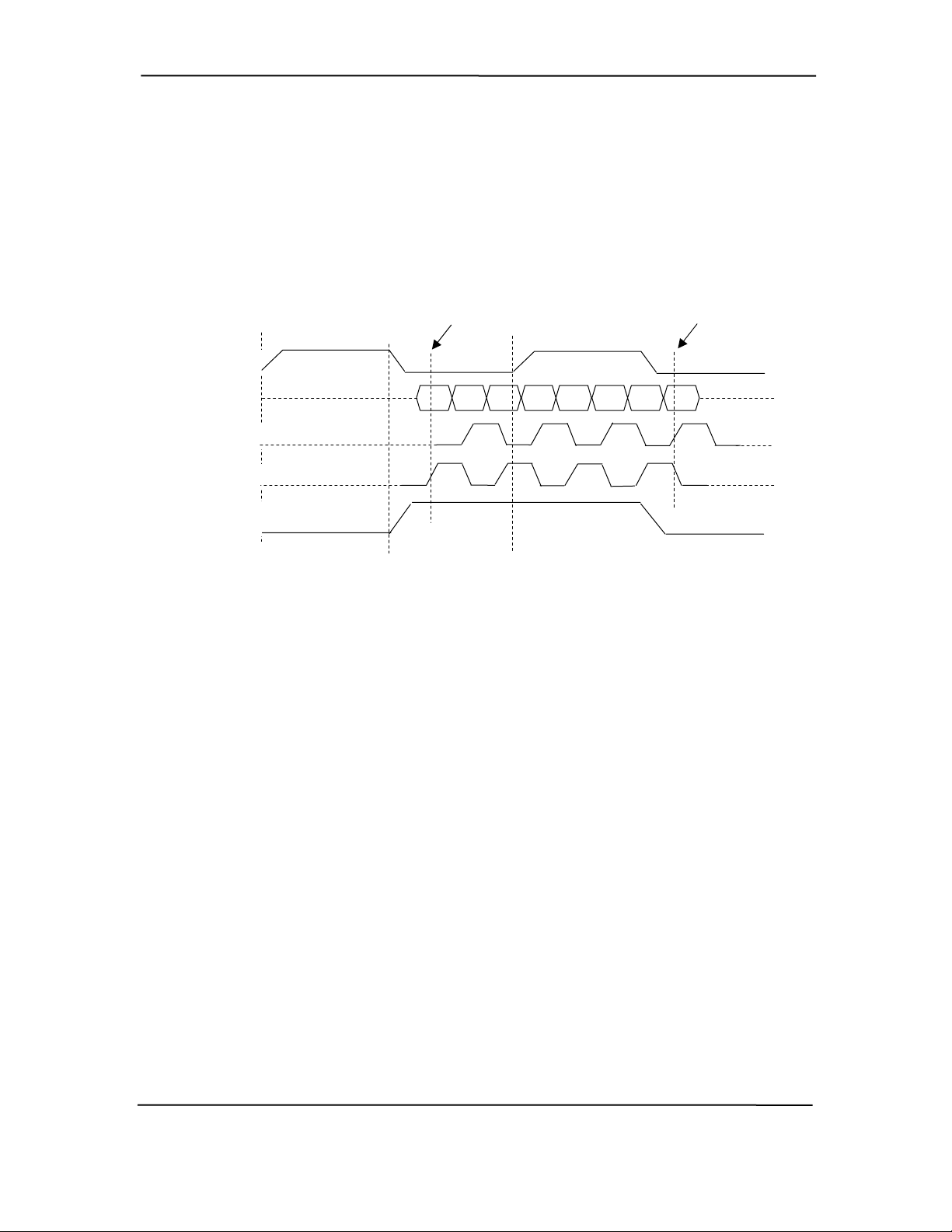
Chapter 4 System Support
t
AGP 8X Transfers
The AGP 8X transfer rate (supported on d325 models only) allows 32 bytes of data to be
transferred in one clock cycle. As with the other transfer rates the 66-MHz CLK signal is used
only for qualifying control signals while strobe signals are used to latch each 4-byte transfer on
the AD lines. As shown in Figure 4-8, 4-byte block DnA is latched by the falling edge of
AD_STBx while DnB is latched by the falling edge of AD_STBx-. The signal level for AGP 8X
transfers can be 0.8 or 1.5 VDC.
CLK
AD
AD_STBS
AD_STBF
TRDY
s
Data
1
Latched
T1
D1A D2A D1B D3A D3B D4A D4B D2B
Final Data
Latched
T2
Figure 4-8. AGP 8X Data Transfer (Peak Transfer Rate: 2128 MB/s)
Compaq D315 and hp d325 Personal Computers
4-12
Featuring the AMD Athlon XP Processor
Second Edition – April 2003
Page 63

Technical Reference Guide
4.3.2 AGP CONNECTOR
Figure 4-8 shows the system’s keyed AGP connector that accepts only 1.5-volt AGP adapters.
The pin out is listed in Table 4-4.
B94
A1
A41
A46
A94
B41
B46
B1
Figure 4-9. AGP Bus Connector
A66
B66
Table 4-4. AGP Bus Connector Pinout
Pin A Signal B Signal Pin A Signal B Signal Pin A Signal B Signal
01 +12 VDC OVRCNT- 23 GND GND 45 VDD3 VDD3
02 Type Det- VDD 24 NC VDD3 Aux 46 TRDY- DEVSEL03 NC VDD 25 VDD3 VDD3 47 STOP- VDDQ
04 USBN USBP 26 PAD30 PAD31 48 PME- PERR05 GND GND 27 PAD28 PAD29 49 GND GND
06 INTA- INTB- 28 VDD3 VDD3 50 PAR SERR07 RESET CLK 29 PAD26 PAD27 51 PAD15 CBE108 GNT- REQ- 30 PAD24 PAD25 52 VDDQ VDDQ
09 VDD3 VDD3 31 GND GND 53 PAD13 PAD14
10 ST1 ST0 32 AD_STB1- AD_STB1 54 PAD11 PAD12
11 NC ST2 33 CBE3- PAD23 55 GND GND
12 PIPE- RBF- 34 VDDQ VDDQ 56 PAD09 PAD10
13 GND GND 35 PAD22 PAD21 57 CBE0- PAD08
14 WBF- NC 36 PAD20 PAD19 58 VDDQ VDDQ
15 SBA1 SBA0 37 GND GND 59 AD_STB0- AD_STB0
16 VDD3 VDD3 38 PAD18 PAD17 60 PAD06 PAD07
17 SBA3 SBA2 39 PAD16 CBE2- 61 GND GND
18 SB_STB- SB_STB 40 VDDQ VDDQ 62 PAD04 PAD05
19 GND GND 41 FRAME- IRDY- 63 PAD02 PAD03
20 SBA5 SBA4 42 NC VDD3 Aux 64 VDDQ VDDQ
21 SBA7 DBA6 43 GND GND 65 PAD00 PAD01
22 NC NC 44 NC NC 66 VREFGC VREFCG
NOTES:
NC = Not connected
VDDQ = 3.3 VDC when TYPE DET- is left open by AGP 1X/2X card.
VDDQ = 1.5 VDC when TYPE DET- is grounded by AGP 4X card.
= Keyed spaces on 1.5-volt AGP connector.
Table 4-4.
AGP Bus Connector Pinout
Compaq D315 and hp d325 Personal Computers
Second Edition - April 2003
4-13
Featuring the AMD Athlon XP Processor
Page 64
Chapter 4 System Support
4.4 SYSTEM RESOURCES
This section describes the availability and basic control of major subsystems, otherwise known as
resource allocation or simply “system resources.” System resources are provided on a priority
basis through hardware interrupts and DMA requests and grants.
4.4.1 INTERRUPTS
The microprocessor uses two types of hardware interrupts; maskable and nonmaskable. A
maskable interrupt can be enabled or disabled within the microprocessor by the use of the STI and
CLI instructions. A nonmaskable interrupt cannot be masked off within the microprocessor,
although it may be inhibited by hardware or software means external to the microprocessor.
4.4.1.1 Maskable Interrupts
The maskable interrupt is a hardware-generated signal used by peripheral functions within the
system to get the attention of the microprocessor. Peripheral functions produce a unique INTA-H
(PCI) or IRQ0-15 (ISA) signal that is routed to interrupt processing logic that asserts the interrupt
(INTR-) input to the microprocessor. The microprocessor halts execution to determine the source
of the interrupt and then services the peripheral as appropriate.
Figure 4-9 shows the routing of PCI and ISA interrupts. Most IRQs are routed through the I/O
controller, which contains a serializing function. A serialized interrupt stream is applied to the
MCP component.
I/O &
IRQ3..7,
9..12,
14,15
SM Functions
PCI Peripherals
IDE
Hard Drives
IRQ14,15
INTA-..H-
LPC47B367
I/O Cntlr.
Interrupt
Serializer
Serial IRQ
MCP
INTR-
APIC bus
Processor
Interrupt
Processing
Figure 4-10. Maskable Interrupt Processing, Block Diagram
Interrupts may be processed in one of two modes (selectable through the F10 Setup utility):
♦ 8259 mode
♦ APIC mode
Compaq D315 and hp d325 Personal Computers
4-14
Featuring the AMD Athlon XP Processor
Second Edition – April 2003
Page 65

Technical Reference Guide
8259 Mode
The 8259 mode handles interrupts IRQ0-IRQ15 in the legacy (AT-system) method using 8259equivalent logic. Table 4-5 lists the standard source configuration for maskable interrupts and
their priorities in 8259 mode. If more than one interrupt is pending, the highest priority (lowest
number) is processed first.
Table 4-5. Maskable Interrupt Priorities and Assignments
Table 4-5.
Maskable Interrupt Priorities and Assignments
Priority Signal Label Source (Typical)
1 IRQ0 Interval timer 1, counter 0
2 IRQ1 Keyboard
3 IRQ8- Real-time clock
4 IRQ9 Unused
5 IRQ10 PCI devices/slots
6 IRQ11 Audio codec
7 IRQ12 Mouse (PS/2)
8 IRQ13 Coprocessor (math)
9 IRQ14 Primary IDE controller
10 IRQ15 Secondary IDE I/F controller
11 IRQ3 Serial port (COM2)
12 IRQ4 Serial port (COM1)
13 IRQ5 Network interface controller
14 IRQ6 Diskette drive controller
15 IRQ7 Parallel port (LPT1)
-- IRQ2 NOT AVAILABLE (Cascade from interrupt controller 2)
APIC Mode
The Advanced Programmable Interrupt Controller (APIC) mode provides enhanced interrupt
processing with the following advantages:
♦ Eliminates the processor’s interrupt acknowledge cycle by using a separate (APIC) bus
♦ Programmable interrupt priority
♦ Additional interrupts (total of 24)
The APIC mode accommodates five PCI interrupt signals (INTA-..INTE-) for use by PCI devices.
The PCI interrupts are evenly distributed to minimize latency and wired as follows:
MCP
Int. Cntlr.
INTA- INTA- INTD- INTC- INTBINTB- INTB- INTA- INTD- —
INTC- INTC- INTB- INTA- —
INTD- INTD- INTC- INTB- —
INTE- — — — INTA-
NOTE:
Internal functions of the MCP (USB, MAC, SMBus, Audio, IDE controllers) use INTA-.
Wired
to
PCI
Slot 1
PCI
Slot 2
PCI
Slot 3
AGP
Slot
Compaq D315 and hp d325 Personal Computers
Second Edition - April 2003
4-15
Featuring the AMD Athlon XP Processor
Page 66

Chapter 4 System Support
The PCI interrupts can be configured by PCI Configuration Registers 60h..63h to share the
standard ISA interrupts (IRQn).
NOTE: The APIC mode is supported by the Windows NT, Windows 2000, and
Windows XP operating systems. Systems running the Windows 95 or 98 operating
system will need to run in 8259 mode.
Maskable interrupt processing is controlled and monitored through standard AT-type I/O-mapped
registers. These registers are listed in Table 4-6.
Table 4-6. Maskable Interrupt Control Registers
Table 4-6.
Maskable Interrupt Control Registers
I/O Port Register
020h Base Address, Int. Cntlr. 1
021h Initialization Command Word 2-4, Int. Cntlr. 1
0A0h Base Address, Int. Cntlr. 2
0A1h Initialization Command Word 2-4, Int. Cntlr. 2
The initialization and operation of the interrupt control registers follows standard AT-type
protocol.
4.4.1.2 Non-Maskable Interrupts
Non-maskable interrupts cannot be masked (inhibited) within the microprocessor itself but may be
maskable by software using logic external to the microprocessor. There are two non-maskable
interrupt signals: the NMI- and the SMI-. These signals have service priority over all maskable
interrupts, with the SMI- having top priority over all interrupts including the NMI-.
NMI- Generation
The Non-maskable Interrupt (NMI-) signal can be generated by one of the following actions:
♦ Parity errors detected on a PCI bus (activating SERR- or PERR-).
♦ Microprocessor internal error (activating IERRA or IERRB)
The SERR- and PERR- signals are routed through the MCP or MCP-2 component, which in turn
activates the NMI to the microprocessor.
Compaq D315 and hp d325 Personal Computers
4-16
Featuring the AMD Athlon XP Processor
Second Edition – April 2003
Page 67
Technical Reference Guide
The NMI Status Register at I/O port 061h contains NMI source and status data as follows:
NMI Status Register 61h
Bit Function
7 NMI Status:
0 = No NMI from system board parity error.
1 = NMI requested, read only
6 IOCHK- NMI:
0 = No NMI from IOCHK-
1 = IOCHK- is active (low), NMI requested, read only
5 Interval Timer 1, Counter 2 (Speaker) Status
4 Refresh Indicator (toggles with every refresh)
3 IOCHK- NMI Enable/Disable:
0 = NMI from IOCHK- enabled
1 = NMI from IOCHK- disabled and cleared (R/W)
2 System Board Parity Error (PERR/SERR) NMI Enable:
0 = Parity error NMI enabled
1 = Parity error NMI disabled and cleared (R/W)
1 Speaker Data (R/W)
0 Inteval Timer 1, Counter 2 Gate Signal (R/W)
0 = Counter 2 disabled
1 = Counter 2 enabled
Functions not related to NMI activity.
After the active NMI has been processed, status bits <7> or <6> are cleared by pulsing bits <2> or
<3> respectively.
The NMI Enable Register (070h, <7>) is used to enable/disable the NMI signal. Writing 80h to
this register masks generation of the NMI-. Note that the lower six bits of register at I/O port 70h
affect RTC operation and should be considered when changing NMI- generation status.
SMI- Generation
The SMI- (System Management Interrupt) is typically used for power management functions.
When power management is enabled, inactivity timers are monitored. When a timer times out,
SMI- is asserted and invokes the microprocessor’s SMI handler. The SMI handler works with the
APM BIOS to service the SMI- according to the cause of the timeout.
Although the SMI- is primarily used for power management the interrupt is also employed for the
QuickLock/QuickBlank functions as well.
Compaq D315 and hp d325 Personal Computers
Second Edition - April 2003
4-17
Featuring the AMD Athlon XP Processor
Page 68

Chapter 4 System Support
4.4.2 DIRECT MEMORY ACCESS
Direct Memory Access (DMA) is a method by which a device accesses system memory without
involving the microprocessor. Although the DMA method has been traditionally used to transfer
blocks of data to or from an ISA I/O device, PCI devices may also use DMA operation as well.
The DMA method reduces the amount of CPU interactions with memory, freeing the CPU for
other processing tasks.
NOTE: This section describes DMA in general. For detailed information regarding
DMA operation, refer to the data manual for the Intel MCP component.
The MCP component includes the equivalent of two 8237 DMA controllers cascaded together to
provide eight DMA channels, each (excepting channel 4) configurable to a specific device. Table
4-7 lists the default configuration of the DMA channels.
Table 4-7. Default DMA Channel Assignments
Table 4-7.
Default DMA Channel Assignments
DMA Channel Device ID
Controller 1 (byte transfers)
0
1
2
3
Controller 2 (word transfers)
4
5
6
7
All channels in DMA controller 1 operate at a higher priority than those in controller 2. Note that
channel 4 is not available for use other than its cascading function for controller 1. The DMA
controller 2 can transfer words only on an even address boundary. The DMA controller and page
register define a 24-bit address that allows data transfers within the address space of the CPU.
In addition to device configuration, each channel can be configured (through PCI Configuration
Registers) for one of two modes of operation:
♦ ♦ LPC DMA
PC/PCI DMA
The LPC DMA mode uses the LPC bus to communicate DMA channel control and is
implemented for devices using DMA through the LPC47B367 I/O controller such as the diskette
drive controller.
The PC/PCI DMA mode uses the REQ#/GNT# signals to communicate DMA channel control and
is used by PCI expansion devices.
Spare
Audio subsystem
Diskette drive
Parallel port
Cascade for controller 1
Spare
Spare
Spare
Compaq D315 and hp d325 Personal Computers
4-18
Featuring the AMD Athlon XP Processor
Second Edition – April 2003
Page 69

Technical Reference Guide
The DMA logic is accessed through two types of I/O mapped registers; page registers and
controller registers.
4.4.2.1 DMA Page Registers
The DMA page register contains the eight most significant bits of the 24-bit address and works in
conjunction with the DMA controllers to define the complete (24-bit) address for the DMA
channels. Table 4-8 lists the page register port addresses.
Table 4-8. DMA Page Register Addresses
Table 4-8.
DMA Page Register Addresses
DMA Channel Page Register I/O Port
Controller 1 (byte transfers)
Ch 0
Ch 1
Ch 2
Ch 3
Controller 2 (word transfers)
Ch 4
Ch 5
Ch 6
Ch 7
Refresh 08Fh [see note]
NOTE:
The DMA memory page register for the refresh channel must be
programmed with 00h for proper operation.
The memory address is derived as follows:
24-Bit Address - Controller 1 (Byte Transfers)
8-Bit Page Register
8-Bit DMA Controller
A23..A16 A15..A00
24-Bit Address - Controller 2 (Word Transfers)
8-Bit Page Register
16-Bit DMA Controller
A23..A17 A16..A01, (A00 = 0)
Note that address line A16 from the DMA memory page register is disabled when DMA
controller 2 is selected. Address line A00 is not connected to DMA controller 2 and is always 0
when word-length transfers are selected.
By not connecting A00, the following applies:
♦ The size of the the block of data that can be moved or addressed is measured in 16-bits
(words) rather than 8-bits (bytes).
♦ The words must always be addressed on an even boundary.
087h
083h
081h
082h
n/a
08Bh
089h
08Ah
Compaq D315 and hp d325 Personal Computers
Second Edition - April 2003
4-19
Featuring the AMD Athlon XP Processor
Page 70

Chapter 4 System Support
DMA controller 1 can move up to 64 Kbytes of data per DMA transfer. DMA controller 2 can
move up to 64 Kwords (128 Kbytes) of data per DMA transfer. Word DMA operations are only
possible between 16-bit memory and 16-bit peripherals.
The RAM refresh is designed to perform a memory read cycle on each of the 512 row addresses
in the DRAM memory space. Refresh operations are used to refresh memory on the 32-bit
memory bus and the ISA bus. The refresh address is provided on lines SA00 through SA08.
Address lines LA23..17, SA18,19 are driven low.
The remaining address lines are in an undefined state during the refresh cycle. The refresh
operations are driven by a 69.799-KHz clock generated by Interval Timer 1, Counter 1. The
refresh rate is 128 refresh cycles in 2.038 ms.
4.4.2.2 DMA Controller Registers
Table 4-9 lists the DMA Controller Registers and their I/O port addresses. Note that there is a set
of registers for each DMA controller.
Table 4-9. DMA Controller Registers
DMA Controller Registers
Register Controller 1 Controller 2 R/W
Status 008h 0D0h R
Command 008h 0D0h W
Mode 00Bh 0D6h W
Write Single Mask Bit 00Ah 0D4h W
Write All Mask Bits 00Fh 0DEh W
Software DRQx Request 009h 0D2h W
Base and Current Address - Ch 0 000h 0C0h W
Current Address - Ch 0 000h 0C0h R
Base and Current Word Count - Ch 0 001h 0C2h W
Current Word Count - Ch 0 001h 0C2h R
Base and Current Address - Ch 1 002h 0C4h W
Current Address - Ch 1 002h 0C4h R
Base and Current Word Count - Ch 1 003h 0C6h W
Current Word Count - Ch 1 003h 0C6h R
Base and Current Address - Ch 2 004h 0C8h W
Current Address - Ch 2 004h 0C8h R
Base and Current Word Count - Ch 2 005h 0CAh W
Current Word Count - Ch 2 005h 0CAh R
Base and Current Address - Ch 3 006h 0CCh W
Current Address - Ch 3 006h 0CCh R
Base and Current Word Count - Ch 3 007h 0CEh W
Current Word Count - Ch 3 007h 0CEh R
Temporary (Command) 00Dh 0DAh R
Reset Pointer Flip-Flop (Command) 00Ch 0D8h W
Master Reset (Command) 00Dh 0DAh W
Reset Mask Register (Command) 00Eh 0DCh W
Table 4-9.
Compaq D315 and hp d325 Personal Computers
4-20
Featuring the AMD Athlon XP Processor
Second Edition – April 2003
Page 71

Technical Reference Guide
4.5 SYSTEM CLOCK DISTRIBUTION
This system uses clock synthesizers in the IGP and the MCP or MCP-2 components. A 14.31818MHz crystal provides an input for clock circuits of the MCP.
Table 4-10 lists clock signals that are distributed between system board components. Frequencies
that are used only internally in chips and components are not listed.
Table 4-10. Clock Generation and Distribution
Table 4-10.
Clock Generation and Distribution
Frequncy Source Destination or Function
266 MHz IGP AGP feedback clock
200 MHz IGP/MCP Hyper Transport Bus clock
133 / 166 MHz [1] IGP Processor, DIMM sockets
66 MHz IGP AGP slot
33 MHz IGP APIC clock
32.768 MHz Crystal MCP, super I/O
25 MHz Crystal NIC PHY
25 MHz NIC PHY MCP
24.576 MHz Crystal Audio codec
16 MHz IGP APIC clock
14.31818 MHz Crystal MCP
14.31818 MHz MCP Clock buffer
14.31818 MHz Clock buffer IGP, super I/O
12.288 MHz Audio codec AC link clock
NOTE:
[1] D315 / d325
These systems uses the spread-spectrum feature of the IGP component. This feature allows BIOS
to set a down spread (0.9 % on the D315, 0.5 % on the d325) to lower the possible effects of high
frequency EMI. Clocks affected by the spread include those used by the processor, memory, and
AGP.
Compaq D315 and hp d325 Personal Computers
Second Edition - April 2003
4-21
Featuring the AMD Athlon XP Processor
Page 72

Chapter 4 System Support
CMOS
4.6 REAL-TIME CLOCK AND CONFIGURATION MEMORY
The Real-time clock (RTC) and configuration memory (also referred to as “CMOS”) functions are
provided by the MCP component and is MC146818-compatible. As shown in the following
figure, the MCP component provides 256 bytes of battery-backed RAM divided into two 128-byte
configuration memory areas. The RTC uses the first 14 bytes (00-0Dh) of the standard memory
area. All locations of the standard memory area (00-7Fh) can be directly accessed using
conventional OUT and IN assembly language instructions through I/O ports 70h/71h, although the
suggested method is to use the INT15 AX=E823h BIOS call.
0Dh
0Ch
0Bh
0Ah
09h
08h
07h
06h
05h
04h
03h
02h
01h
00h
Register D
Register C
Register B
Register A
Year
Month
Date of Month
Day of Week
Hours (Alarm)
Hours (Timer)
Minutes (Alarm)
Minutes (Timer)
Seconds (Alarm)
Seconds (Timer)
Figure 4-11. Configuration Memory Map
MCP
Extended Config.
Memory Area
(128 bytes)
Standard Config.
Memory Area
(114 bytes)
RTC Area
(14 bytes)
FFh
80h
7Fh
0Eh
0Dh
00h
A lithium 3-VDC battery is used for maintaining the RTC and configuration memory while the
system is powered down. The battery is located in a battery holder on the system board and has a
life expectancy of about three years. When the battery has expired it is replaced with a Renata
CR2032 or equivalent 3-VDC lithium battery.
4.6.1 CLEARING CMOS
The contents of configuration memory (including the Power-On Password) can be cleared by the
following procedure:
1. Turn off the unit and disconnect the AC power cord from the outlet and/or system unit.
2. Remove the chassis hood (cover) and insure that no LEDs on the system board are
illuminated.
3. On the JBAT1 header, move the jumper from pins 1 and 2 to pins 2 and 3. Leave the jumper
on pins 2 and 3 for about 5 seconds. This action will ground the battery input to the CMOS
circuitry.
4. Replace the jumper onto pins 1 and 2.
5. Replace the chassis hood (cover).
6. Reconnect the AC power cord to the outlet and/or system unit and reboot the system.
To clear only the Power-On Password refer to section 4.7.1.1.
Compaq D315 and hp d325 Personal Computers
4-22
Featuring the AMD Athlon XP Processor
Second Edition – April 2003
Page 73

Technical Reference Guide
4.6.2 CMOS ARCHIVE AND RESTORE
During the boot process the BIOS saves a copy of CMOS to the flash ROM. If the system
becomes unusable, the last good copy of CMOS can be recalled using the power-override function
as follows:
1. With the unit powered down, press and release the power button to initiate the boot sequence.
2. Immediately after releasing the power button, press it again and hold (typically at least four
seconds) until the unit powers off again. This action will be recorded as a power button
override event.
3. Press and release the power button once more, initiating the boot sequence that should detect
the occurrence of an override event and load the backup copy of CMOS, allowing the system
to boot.
4.6.3 STANDARD CMOS LOCATIONS
Table 4-11 and the following paragraphs describe standard configuration memory locations 0Ah3Fh. These locations are accessible through using OUT/IN assembly language instructions using
port 70/71h or BIOS function INT15, AX=E823h.
Table 4-11. Configuration Memory (CMOS) Map
Table 4-11.
Configuration Memory (CMOS) Map
Location Function Location Function
00-0Dh Real-time clock 24h System board ID
0Eh Diagnostic status 25h System architecture data
0Fh System reset code 26h Auxiliary peripheral configuration
10h Diskette drive type 27h Speed control external drive
11h Reserved 28h Expanded/base mem. size, IRQ12
12h Hard drive type 29h Miscellaneous configuration
13h Security functions 2Ah Hard drive timeout
14h Equipment installed 2Bh System inactivity timeout
15h Base memory size, low byte/KB 2Ch Monitor timeout, Num Lock Cntrl
16h Base memory size, high byte/KB 2Dh Additional flags
17h Extended memory, low byte/KB 2Eh-2Fh Checksum of locations 10h-2Dh
18h Extended memory, high byte/KB 30h-31h Total extended memory tested
19h Hard drive 1, primary controller 32h Century
1Ah Hard drive 2, primary controller 33h Miscellaneous flags set by BIOS
1Bh Hard drive 1, secondary controller 34h International language
1Ch Hard drive 2, secondary controller 35h APM status flags
1Dh Enhanced hard drive support 36h ECC POST test single bit
1Eh Reserved 37h-3Fh Power-on password
1Fh Power management functions 40-FFh Feature Control/Status
NOTES:
Assume unmarked gaps are reserved.
Higher locations (>3Fh) contain information that should be accessed using the INT15, AX=E845h
BIOS function (refer to Chapter 8 for BIOS function descriptions).
Compaq D315 and hp d325 Personal Computers
Second Edition - April 2003
4-23
Featuring the AMD Athlon XP Processor
Page 74

Chapter 4 System Support
4.7 SYSTEM MANAGEMENT
This section describes functions having to do with security, power management, temperature, and
overall status. These functions are handled by hardware and firmware (BIOS) and generally
configured through the Setup utility.
4.7.1 SECURITY FUNCTIONS
This system includes various features that provide different levels of security. Note that this
subsection describes only the hardware functionality (including that supported by Setup) and
does not describe security features that may be provided by the operating system and application
software.
4.7.1.1 Power-On Password
This system includes a power-on password, which may be enabled or disabled (cleared) through a
jumper on the system board. The password is stored in configuration memory (CMOS) and if
enabled and then forgotten will require that either the password be cleared (preferable solution
and described below) or the entire CMOS be cleared (refer to section 4.6).
To clear only the password, use the following procedure:
1. Turn off the system and disconnect the AC power cord from the outlet and/or system unit.
2. Remove the cover (hood) as described in the appropriate User Guide or Service Reference
Guide. Insure that any system board LEDs are off (not illuminated).
3. Locate the password clear header labeled JCMOS1 and move the jumper from pins 1 and 2 to
pins 2 and 3.
4. Replace the cover.
5. Re-connect the AC power cord to the AC outlet and/or system unit.
6. Turn on the system. The POST routine will clear and disable the password.
7. To re-enable the password feature, repeat steps 1-6, replacing the jumper on pins 1 and 2 of
header JCMOS1.
4.7.1.2 Setup Password
The Setup utility may be configured to be always changeable or changeable only by entering a
password. The password is held on CMOS and, if forgotten, will require that CMOS be cleared
(refer to section 4.6).
Compaq D315 and hp d325 Personal Computers
4-24
Featuring the AMD Athlon XP Processor
Second Edition – April 2003
Page 75

Technical Reference Guide
4.7.1.3 Cable Lock Provision
These systems include a chassis cutout (on the rear panel) for the attachment of a cable lock
mechanism.
4.7.1.4 I/O Interface Security
The serial, parallel, USB, and diskette interfaces may be disabled individually through the Setup
utility to guard against unauthorized access to a system. In addition, the ability to write to or boot
from a removable media drive (such as the diskette drive) may be enabled through the Setup
utility. The disabling of the serial, parallel, and diskette interfaces are a function of the
LPC47B367 I/O controller. The USB ports are controlled through the MCP.
Compaq D315 and hp d325 Personal Computers
Second Edition - April 2003
4-25
Featuring the AMD Athlon XP Processor
Page 76

Chapter 4 System Support
4.7.2 POWER MANAGEMENT
This system provides baseline hardware support of ACPI- and APM-compliant firmware and
software. Key power-consuming components (processor, chipset, I/O controller, and fan) can be
placed into a reduced power mode either automatically or by user control. The system can then be
brought back up (“wake-up”) by events defined by the ACPI specification. The ACPI wake-up
events supported by this system are listed as follows:
ACPI Wake-Up Event System Wakes From
Power Button Suspend or soft-off
RTC Alarm Suspend or soft-off
Wake On LAN (w/NIC) Suspend or soft-off
PME Suspend or soft-off
USB Suspend only
Keyboard Suspend only
Mouse Suspend only
4.7.3 SYSTEM STATUS
These systems provide a visual indication of system boot and ROM flash status through the
keyboard LEDs and operational status using bi-colored power and hard drive activity LEDs as
indicated in Tables 4-12 and 4-13 respectively.
NOTE: The LED indications listed in Table 4-13 are valid only for PS/2-type
keyboards. A USB keyboard will not provide LED status for the listed events, although
audible (beep) indications will occur.
Table 4-12. System Boot/ROM Flash Status LED Indications
System Boot/ROM Flash Status LED Indications
Event
System memory failure [1] Blinking Off Off
Graphics controller failure [2] Off Blinking Off
System failure prior to graphics cntlr. initialization [3] Off Off Blinking
ROMPAQ diskette not present, faulty, or drive prob. On Off Off
Password prompt Off On Off
Invalid ROM detected - flash failed Blinking [4] Blinking [4] Blinking [4]
Keyboard locked in network mode Blinking [5] Blinking [5] Blinking [5]
Successful boot block ROM flash On [6] On [6] On [6]
NOTES:
[1] Accompanied by 1 short, 2 long audio beeps
[2] Accompanied by 1 long, 2 short audio beeps
[3] Accompanied by 2 long, 1 short audio beeps
[4] All LEDs will blink in sync twice, accompanied by 1 long and three short audio beeps
[5] LEDs will blink in sequence (NUM Lock, then CAPs Lock, then Scroll Lock)
[6] Accompanied by rising audio tone.
Compaq D315 and hp d325 Personal Computers
4-26
Featuring the AMD Athlon XP Processor
Second Edition – April 2003
Table 4-12.
NUM Lock
LED
CAPs Lock
LED
Scroll Lock
LED
Page 77

Technical Reference Guide
Table 4-13. System Operational Status LED Indication
Table 4-13.
System Operational Status LED Indications
System Status
S0: System on (normal operation) Steady green Steady green
S1: Suspend Blinks green @ .5 Hz Blinks green @ .5 Hz
S3: Suspend to RAM Blinks green @ .5 Hz Blinks green @ .5 Hz
S4: Suspend to disk Off Off
S5: Soft off Off Off
Processor not seated or installed Steady red Steady red
CPU thermal shutdown See note [1] See note [1]
No memory installed Blinks red @ 2 Hz Blinks red @ 2 Hz
Memory error na See note [2]
ROM flashing See note [3] See note [3]
Video error na See note [4]
PCA failure na See note [5]
Invalid ROM checksum error na See note [6]
System off Off Off
For both systems, HD LED is on (green) during hrd rive activity, off at all other times.
[2] Sequence; blinks red five times in five seconds followed by two-second pause.
[3] Steady red when flashing ROM, then blinks green every second indicating user can restart.
[4] Sequence; blinks red six times in six seconds followed by two-second pause.
[5] Sequence; blinks red seven times in seven seconds followed by two-second pause.
[6] Sequence; blinks red eight times in eight seconds followed by two-second pause.
NOTE:
[1] Sequence; blinks red every second for 2 seconds, then off for two seconds.
D315
Power LED
d325
Power LED
4.7.4 THERMAL SENSING AND COOLING
These systems feature variable-speed fans that are controlled through temperature sensing logic
on the system board and/or in the power supply. Typical cooling conditions include the
following:
1. Normal – Low fan speed.
2. Hot processor – ASIC directs Speed Control logic to increase speed of fan(s).
3. Hot power supply – Power supply increases speed of fan(s).
4. Sleep state – Fan(s) turned off. Hot processor or power supply will result in starting fan(s).
High and low thermal parameters are programmed into the ASIC by BIOS during POST. If the
high thermal parameter is reached then the fan(s) will be turned on full speed and the Thermsignal will be asserted.
The system board provides connections for a heatsink-mounted CPU fan and a chassis fan, both
which complement the power supply fan. The system supports the use of variable-speed fans that
are regulated according to the temperature measured by an AMD1030 temperature controller.
Compaq D315 and hp d325 Personal Computers
Second Edition - April 2003
4-27
Featuring the AMD Athlon XP Processor
Page 78
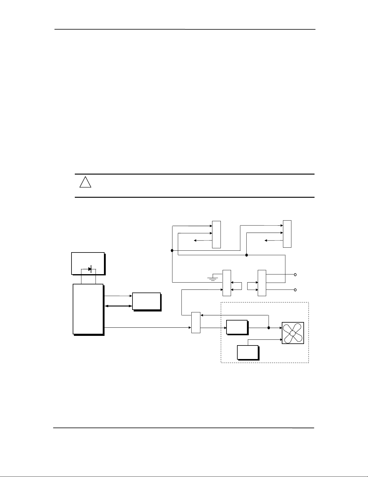
Chapter 4 System Support
p
4.7.4.1 Cooling for D315 Models
The temperature controller produces the Fan CMD (which varies from 0 to +2.5 VDC) that is
applied to the speed control circuitry of the power supply assembly. The output of the speed
control circuitry controls the power supply assembly’s internal fan and is also routed back to the
system board and, in the default jumper configuration, is applied as the Fan Sink signal to the
negative terminal of the connected fans. The default jumper configuration also applies + 5 VDC to
the positive terminal of the fans. With the Fan CMD signal being varied from +0.5 to -7 VDC, the
chassis and CPU fans will be driven by a voltage from about +5 to +12 VDC, depending on the
processor temperature.
In a characteristically warm environment or should the speed regulation circuitry be inadequate or
fail it may be desirable to have the fans driven by a constant +12 VDC by configuring both
FAN_SEL jumpers to pins 1 and 2.
Note that the power supply assembly fan operates independently of the CPU and chassis fans.
CAUTION: Both FAN_SELn jumpers must have the same configuration (jumpers on
the same pins). Different jumper settings (one jumper on pins 1 and 2 and the other
jumper on pins 2 and 3) may result in equipment damage.
TACH function of the fan(s) not used.
Processor
AMD1030
Temp.
Controller
NOTES: Jumpers shown in standard configuration.
Therm-
SMBus
Super
I/O Cntlr.
Fan CMD
Fan Pwr
TACH
NC
Fan Sink
PWR_FAN
1
2
Chassis Fan
Header
(-)
1
(+)
2
3
FAN_SEL1
Header/Jumper
Fan
Sink
Fan
CMD
Fan Pwr
NC
FAN_SEL2
Header/Jum
1
2
3
Power Supply Assembly
Speed
Control
+5 VDC
PS
Circuits
1
2
3
CPU Fan
(-)
(+)
TACH
er
(-)
(+)
Header
1
2
3
+12 VDC
+5 VDC
PS Fan
Figure 4-12. D315 Model Fan Control Block Diagram
Compaq D315 and hp d325 Personal Computers
4-28
Featuring the AMD Athlon XP Processor
Second Edition – April 2003
Page 79

Technical Reference Guide
4.7.4.2 Cooling for d325 Models
The fan control logic on the d325 model differs from the D315 system in that fans are controlled
by the system board logic. The fans are driven by a constant positive 12 volts on one side and a
negative voltage that is variable through the Fan Cntrl logic. A Hardware Monitor ASIC monitors
the temperature of the processor and changes the duty cycle of the Fan PWM to increase or
decrease fan speed based on the processor temperature. The Fan Clamp signal is initiated by the
BIOS and produced by the GPIO at boot time to ensure that the fans start at boot time.
NOTE: A protection mechanism is provided where the processor threshold
temperature programmed into the Hardware Monitor ASIC is temporarily set by the
BIOS to a lower than normal level during the initial start up to protect against the
possibility of an incorrectly installed heat sink. If during the boot period the processor’s
temperature reaches 100° C the hardware Monitor will assert the Therm signal causing
the I/O Controller to de-assert the PS On signal, which will shut down the power supply.
If the processor does not reach 100° C during the boot sequence the BIOS then re-sets
the thermal threshold to the run-time level of 125° C
+12 VDC
LPC47B367
I/O
Controller
Therm
CPU
Fan Tach
Chassis
Fan Tach
PS On
Fan
Clamp
Fan PWM
Tach Logic
Fan
Cntrl
Fan
Header P70
(-)
(+)
Sense
CPU Fan
1
2
3
Header
1
2
ATX Power
+12 VDC
Tach Logic
Fan Sink
Speed
Control
Hardware
Monitor
ASIC
Processor
14
PS On
Chassis Fan
Header P8
(-)
1
(+)
Sense
Power Supply Assembly
PS
Circuits
2
3
+5 VDC
(-)
(+)
PS Fan
Figure 4-13. d325 Model Fan Control Functional Block Diagram
Compaq D315 and hp d325 Personal Computers
Featuring the AMD Athlon XP Processor
Second Edition - April 2003
4-29
Page 80

Chapter 4 System Support
4.8 REGISTER MAP AND MISCELLANEOUS FUNCTIONS
This section contains the system I/O map and information on general-purpose functions of the
MCP and I/O controller.
4.8.1 SYSTEM I/O MAP
Table 4-14 lists the fixed addresses of the input/output (I/O) ports.
Table 4-14. System I/O Map
Table 4-14.
System I/O Map
I/O Port Function
0000..001Fh DMA Controller 1
0020..002Dh Interrupt Controller 1
002E, 002Fh Index, Data Ports to LPC47B367 I/O Controller (primary)
0030..003Dh Interrupt Controller
0040..0042h Timer 1
004E, 004Fh Index, Data Ports to LPC47B367 I/O Controller (secondary)
0050..0052h Timer / Counter
0060..0067h Microcontroller, NMI Controller (alternating addresses)
0070..0077h RTC Controller
0080..0091h DMA Controller
0092h Port A, Fast A20/Reset Generator
0093..009Fh DMA Controller
00A0..00B1h Interrupt Controller 2
00B2h, 00B3h APM Control/Status Ports
00B4..00BDh Interrupt Controller
00C0..00DFh DMA Controller 2
00F0h Coprocessor error register
0170..0177h IDE Controller 2 (active only if standard I/O space is enabled for primary drive)
01F0..01F7h IDE Controller 1 (active only if standard I/O space is enabled for secondary drive)
0278..027Fh Parallel Port (LPT2)
02E8..02EFh Serial Port (COM4)
02F8..02FFh Serial Port (COM2)
0370..0377h Diskette Drive Controller Secondary Address
0376h IDE Controller 2 (active only if standard I/O space is enabled for primary drive)
0378..037Fh Parallel Port (LPT1)
03B0..03DFh Graphics Controller
03BC..03BEh Parallel Port (LPT3)
03E8..03EFh Serial Port (COM3)
03F0..03F5h Diskette Drive Controller Primary Addresses
03F6h IDE Controller 1 (active only if standard I/O space is enabled for sec. drive)
03F8..03FFh Serial Port (COM1)
04D0, 04D1h Interrupt Controller
0678..067Fh Parallel Port (LPT2)
0778..077Fh Parallel Port (LPT1)
07BC..07BEh Parallel Port (LPT3)
0CF8h PCI Configuration Address (dword access only )
0CF9h Reset Control Register
0CFCh PCI Configuration Data (byte, word, or dword access)
NOTE:
Assume unmarked gaps are unused, reserved, or used by functions that employ variable I/O
address mapping. Some ranges may include reserved addresses.
Compaq D315 and hp d325 Personal Computers
4-30
Featuring the AMD Athlon XP Processor
Second Edition – April 2003
Page 81

Technical Reference Guide
4.8.2 LPC47B367 I/O CONTROLLER FUNCTIONS
The LPC47B367 I/O controller contains various functions such as the keyboard/mouse interfaces,
diskette interface, serial interfaces, and parallel interface. While the control of these interfaces
uses standard AT-type I/O addressing (as described in chapter 5) the configuration of these
functions uses indexed ports unique to the LPC47B367. In these systems, hardware strapping
selects I/O addresses 02Eh and 02Fh at reset as the Index/Data ports for accessing the logical
devices within the LPC47B367. Table 4-15 lists the PnP standard control registers for the
LPC47B367.
Table 4-15 LPC47B367 I/O Controller Registers
Table 4-15.
LPC47B367 I/O Controller Control Registers
Index Function Reset Value
02h Configuration Control 00h
03h Reserved
07h Logical Device (Interface) Select:
00h = Diskette Drive I/F
01h = Reserved
02h = Reserved
03h = Parallel I/F
04h = Serial I/F (UART 1/Port A)
05h = Serial I/F (UART 2/Port B)
06h = Reserved
07h = Keyboard I/F
08h = Reserved
09h = Reserved
0Ah = Runtime Registers (GPIO Config.)
0Bh = SMBus Configuration
20h Super I/O ID Register (SID) 56h
21h Revision -22h Logical Device Power Control 00h
23h Logical Device Power Management 00h
24h PLL / Oscillator Control 04h
25h Reserved
26h Configuration Address (Low Byte)
27h Configuration Address (High Byte)
28-2Fh Reserved
NOTE:
For a detailed description of registers refer to appropriate SMC documentation.
The configuration registers are accessed through I/O registers 2Eh (index) and 2Fh (data) after the
configuration phase has been activated by writing 55h to I/O port 2Eh. The desired interface
(logical device) is initiated by firmware selecting logical device number of theLPC47B347 using
the following sequence:
1. Write 07h to I/O register 2Eh.
2. Write value of logical device to I/O register 2Fh.
3. Write 30h to I/O register 2Eh.
4. Write 01h to I/O register 2Fh (this activates the interface).
Writing AAh to 2Eh deactivates the configuration phase.
00h
Compaq D315 and hp d325 Personal Computers
Second Edition - April 2003
4-31
Featuring the AMD Athlon XP Processor
Page 82

Chapter 4 System Support
The systems covered in this guide utilize the following specialized functions built into the
LPC47B367 I/O Controller:
♦ Power/HD LED status indicators – The I/O controller provides color and blink control for the
front panel LEDs used for indicating system events as listed below. Indications valid for both
D315 and d325 unless otherwise indicated.
System Status Power LED HD LED Beeps
S0: System on (normal operation) Steady green Green w/HD activity None
S1: Suspend Blinks green @ 0.5 Hz Off None
S3: Suspend to RAM Blinks green @ 0.5 Hz Off None
S4: Suspend to disk Off Off None
S5: Soft off Off Off None
Processor not seated Steady red Off None
ROM flashing [1] Off None
No memory installed Blinks red @ 2 Hz Off None
Power supply crowbar activated (D315
only)
CPU thermal shutdown D315 [2], d325 [3]
Memory error (d325 only) See note [4] Off 5
Video error (d325 only) See note [5] Off 6
System board failure (d325 only) See note [6] Off 7
Invalid ROM checksum (d325 only) See note [7] Off 8
System off Off Off None
[1] Red during flash, then blinks green @ 1 Hz when user can reboot.
[2] Repetitive sequence of 2 red blinks @ 1 Hz, followed by 2-second pause.
[3] Repetitive sequence of four red blinks @ 1 Hz followed by 2-second pause
[4] Repetitive sequence of five red blinks @ 1 Hz followed by 2-second pause.
[5] Repetitive sequence of six red blinks @ 1 Hz followed by 2-second pause.
[6] Repetitive sequence of seven red blinks @ 1 Hz followed by 2-second pause.
[7] Repetitive sequence of eight red blinks @ 1 Hz followed by 2-second pause.
NOTES:
Blinks red @ 0.5 Hz Off None
♦ ♦ I/O security – The parallel, serial, and diskette interfaces may be disabled individually by
software and the LPC47B367’s disabling register locked. If the disabling register is locked, a
system reset through a cold boot is required to gain access to the disabling (Device Disable)
register.
Legacy/ACPI power button mode control – The LPC47B367 receives the pulse signal from
the system’s power button and produces the PS On signal according to the mode (legacy or
ACPI) selected. Refer to chapter 7 for more information regarding power management.
Compaq D315 and hp d325 Personal Computers
4-32
Featuring the AMD Athlon XP Processor
Second Edition – April 2003
Page 83

Technical Reference Guide
Chapter 5 INPUT/OUTPUT INTERFACES
5. Chapter 5 INPUT/OUTPUT INTERFACES
5.1 INTRODUCTION
This chapter describes the standard (i.e., system board) interfaces that provide input and output
(I/O) porting of data and specifically discusses interfaces that are controlled through I/O-mapped
registers. The following I/O interfaces are covered in this chapter:
♦ Enhanced IDE interface (5.2) page 5-1
♦ Diskette drive interface (5.3) page 5-4
♦ Serial interfaces (5.4) page 5-8
♦ Parallel interface (5.5) page 5-11
♦ Keyboard/pointing device interface (5.6) page 5-16
♦ Universal serial bus interface (5.7) page 5-22
♦ Audio subsystem (5.8) page 5-26
♦ Network Interface Controller (5.9) page 5-32
5.2 ENHANCED IDE INTERFACE
The enhanced IDE (EIDE) interface consists of primary and secondary controllers integrated into
the south bridge component of the chipset. Two 40-pin IDE connectors (one for each controller)
are included on the system board. Each controller can be configured independently for the
following modes of operation:
♦
Programmed I/O (PIO) mode – CPU controls drive transactions through standard I/O mapped
registers of the IDE drive.
♦
8237 DMA mode – CPU offloads drive transactions using DMA protocol with transfer rates
up to 16 MB/s.
♦
Ultra ATA/100 mode – Preferred bus mastering source-synchronous protocol providing
transfer rates of 100 MB/s.
5.2.1 IDE PROGRAMMING
The IDE interface is configured as a PCI device during POST and controlled through I/O-mapped
registers at runtime. Operating systems other than DOS or Windows may require using Setup
(F10) for drive configuration.
Compaq D315 and hp d325 Personal Computers
Featuring the AMD Athlon XP Processor
Second Edition - April 2003
5-1
Page 84

Chapter 5 Input/Output Interfaces
5.2.1.1 IDE Configuration Registers
The IDE controller is configured as a PCI device with bus mastering capability. The PCI
configuration registers for the IDE controller function (PCI device #9, function #0) are listed in
Table 5-1.
Table 5–1. IDE PCI Configuration Registers
IDE PCI Configuration Registers (MCP, Device 9/Function 0)
PCI Conf.
Addr.
00, 01h Vender ID 10DEh 3Ch Interrupt Line 00h
02, 03h Device ID [1] 3Dh Interrupt Pin 01h
04, 05h PCI Command 0000h 3Eh Minimum Grant 03h
06-07h PCI Status 00B0h 3Fh Maximum Latency 01h
08h Revision ID A1h 40h Write SS Vendor ID 0000h
09 – 0Bh Class Code 01018Ah 42h Write SS ID 0000h
0Ch Cache Line Size 00h 44h Power Mgmt. Config. 01h
0Dh Master Latency Timer 00h 45h Next Item Pointer 00h
0Eh Header Type 00h 46h Power Mgmt. Capabilities E802h
0Fh BIST 00h 48h Power Mgmt. Cntrl./Sts. 0000h
10 – 13h Pri. Cmd. I/O Base Addr. 1d 4Bh Power Mgmt. Data 00h
14 – 17h Pri. Cntrl. I/O Base Addr. 1d 50h IDE Config. 0000h
18 – 1Bh Sec. CMD I/O Base Addr. 1d 58, 59h IDE Timing A8A8h
1C – 1Fh Sec. Cntrl. I/O Base Addr. 1d 5A, 5Bh IDE Timing A8A8h
20h Bus Mstr. I/O Base Addr. 1d 5Ch IDE Cycle & Addr. Timing 00FFh
2Ch Subsystem Vendor ID 0000h 5Dh IDD Cycle & Addr. Timing FFFFh
2Eh Subsystem ID 0000h 60h UDMA Mode Selection 0s
34h Capabilities Pointer 44h - - -
NOTES:
[1] D315 = 01BCh, d325 = 0065h
Register
Table 5-1.
Reset
Value
PCI Conf.
Addr.
Register
Reset
Value
5.2.1.2 IDE Bus Master Control Registers
The IDE interface can perform PCI bus master operations using the registers listed in Table 5-2.
These registers occupy 16 bytes of variable I/O space set by software and indicated by PCI
configuration register 20h in the previous table.
Table 5–2. IDE Bus Master Control Registers
Table 5-2.
IDE Bus Master Control Registers
I/O Addr.
Offset
00h 1 Bus Master IDE Command (Primary) 00h
02h 1 Bus Master IDE Status (Primary) 00h
04h 4 Bus Master IDE Descriptor Pointer (Pri.) 0000 0000h
08h 1 Bus Master IDE Command (Secondary) 00h
0Ah 2 Bus Master IDE Status (Secondary) 00h
0Ch 4 Bus Master IDE Descriptor Pointer (Sec.) 0000 0000h
NOTE:
Unspecified gaps are reserved, will return indeterminate data, and should not be written to.
5-2 Compaq D315 and hp d325 Personal Computers
Featuring the AMD Athlon XP Processor
Size
(Bytes) Register
Second Edition – April 2003
Default
Value
Page 85

Technical Reference Guide
5.2.2 IDE CONNECTOR
This system uses a standard 40-pin connector for the primary IDE device and connects (via a
cable) to the hard drive. Note that some signals are re-defined for UATA/33 and higher modes,
which require a special 80-conductor cable (supplied) designed to reduce cross-talk. Device
power is supplied through a separate connector.
Figure 5-1. 40-Pin Primary IDE Connector (on system board).
Table 5–3. 40-Pin Primary IDE Connector Pinout
Pin Signal Description Pin Signal Description
1 RESET- Reset 21 DRQ DMA Request
2 GND Ground 22 GND Ground
3 DD7 Data Bit <7> 23 IOW- I/O Write [1]
4 DD8 Data Bit <8> 24 GND Ground
5 DD6 Data Bit <6> 25 IOR- I/O Read [2]
6 DD9 Data Bit <9> 26 GND Ground
7 DD5 Data Bit <5> 27 IORDY I/O Channel Ready [3]
8 DD10 Data Bit <10> 28 CSEL Cable Select
9 DD4 Data Bit <4> 29 DAK- DMA Acknowledge
10 DD11 Data Bit <11> 30 GND Ground
11 DD3 Data Bit <3> 31 IRQn Interrupt Request [4]
12 DD12 Data Bit <12> 32 IO16- 16-bit I/O
13 DD2 Data Bit <2> 33 DA1 Address 1
14 DD13 Data Bit <13> 34 DSKPDIAG Pass Diagnostics
15 DD1 Data Bit <1> 35 DA0 Address 0
16 DD14 Data Bit <14> 36 DA2 Address 2
17 DD0 Data Bit <0> 37 CS0- Chip Select
18 DD15 Data Bit <15> 38 CS1- Chip Select
19 GND Ground 39 HDACTIVE- Drive Active (front panel LED) [5]
20 -- Key 40 GND Ground
NOTES:
[1] On UATA/33 and higher modes, re-defined as STOP.
[2] On UATA/33 and higher mode reads, re-defined as DMARDY-.
On UATA/33 and higher mode writes, re-defined as STROBE.
[3] On UATA/33 and higher mode reads, re-defined as STROBE-.
On UATA/33 and higher mode writes, re-defined as DMARDY-.
[4] Primary connector wired to IRQ14, secondary connector wired to IRQ15.
[5] Pin 39 is used for spindle sync and drive activity (becomes SPSYNC/DACT-)
when synchronous drives are connected.
Table 5-3.
40-Pin Primary IDE Connector Pinout
Compaq D315 and hp d325 Personal Computers
5-3
Featuring the AMD Athlon XP Processor
Second Edition - April 2003
Page 86

Chapter 5 Input/Output Interfaces
5.3 DISKETTE DRIVE INTERFACE
The diskette drive interface supports up to two diskette drives, each of which use a common cable
connected to a standard 34-pin diskette drive connector. Models that come standard with a 3.5inch 1.44-MB diskette drive will have the diskette drive installed as drive A. The drive
designation is determined by which connector is used on the diskette drive cable. The drive
attached to the end connector is drive A while the drive attached to the second (next to the end)
connector is drive B.
On all models, the diskette drive interface function is integrated into the LPC47B367 super I/O
component. The internal logic of the I/O controller is software-compatible with standard 82077type logic. The diskette drive controller has three operational phases in the following order:
♦ Command phase - The controller receives the command from the system.
♦ Execution phase - The controller carries out the command.
♦ Results phase - Status and results data is read back from the controller to the system.
The Command phase consists of several bytes written in series from the CPU to the data register
(3F5h/375h). The first byte identifies the command and the remaining bytes define the parameters
of the command. The Main Status register (3F4h/374h) provides data flow control for the diskette
drive controller and must be polled between each byte transfer during the Command phase.
The Execution phase starts as soon as the last byte of the Command phase is received. An
Execution phase may involve the transfer of data to and from the diskette drive, a mechnical
control function of the drive, or an operation that remains internal to the diskette drive controller.
Data transfers (writes or reads) with the diskette drive controller are by DMA, using the DRQ2
and DACK2- signals for control.
The Results phase consists of the CPU reading a series of status bytes (from the data register
(3F5h/375h)) that indicate the results of the command. Note that some commands do not have a
Result phase, in which case the Execution phase can be followed by a Command phase.
During periods of inactivity, the diskette drive controller is in a non-operation mode known as the
Idle phase.
5-4 Compaq D315 and hp d325 Personal Computers
Featuring the AMD Athlon XP Processor
Second Edition – April 2003
Page 87

Technical Reference Guide
5.3.1 DISKETTE DRIVE PROGRAMMING
Programming the diskette drive interface consists of configuration, which occurs typically during
POST, and control, which occurs at runtime.
5.3.1.1 Diskette Drive Interface Configuration
The diskette drive controller must be configured for a specific address and also must be enabled
before it can be used. Address selection and enabling of the diskette drive interface are affected by
firmware through the PnP configuration registers of the LPC47B367 I/O controller during POST.
The configuration registers are accessed through I/O registers 2Eh (index) and 2Fh (data) after the
configuration phase has been activated by writing 55h to I/O port 2Eh. The diskette drive I/F is
initiated by firmware selecting logical device 0 of the LPC47B367 using the following sequence:
1. Write 07h to I/O register 2Eh.
2. Write 00h to I/O register 2Fh (this selects the diskette drive I/F).
3. Write 30h to I/O register 2Eh.
4. Write 01h to I/O register 2Fh (this activates the interface).
Writing AAh to 2Eh deactivates the configuration phase. The diskette drive I/F configuration
registers are listed in the following table:
Table 5–4. Diskette Drive Controller Configuration Registers
Table 5-4.
Diskette Drive Interface Configuration Registers
Index
Address Function
30h Activate R/W 01h
60-61h Base Address R/W 03F0h
70h Interrupt Select R/W 06h
74h DMA Channel Select R/W 02h
F0h DD Mode R/W 02h
F1h DD Option R/W 00h
F2h DD Type R/W FFh
F4h DD 0 R/W 00h
F5h DD 1 R/W 00h
For detailed configuration register information refer to the SMSC data sheet for the LPC47B367
I/O component.
R/W
Reset
Value
5.3.1.2 Diskette Drive Interface Control
The BIOS function INT 13 provides basic control of the diskette drive interface. The diskette
drive interface can be controlled by software through the LPC47B367’s I/O-mapped registers
listed in Table 5-5. The diskette drive controller of the LPC47B367 operates in the PC/AT mode
in these systems.
Compaq D315 and hp d325 Personal Computers
Second Edition - April 2003
5-5
Featuring the AMD Athlon XP Processor
Page 88

Chapter 5 Input/Output Interfaces
Table 5–5. Diskette Drive Interface Control Registers
Diskette Drive Interface Control Registers
Pri.
Addr.
3F0h 370h Status Register A:
3F1h 371h Status Register B:
3F2h 372h Digital Output Register (DOR):
3F3h 373h Tape Drive Register (available for compatibility) R/W
3F4h 374h Main Status Register (MSR):
3F5h 375h Data Register:
3F6h 376h Reserved -3F7h 377h Digital Input Register (DIR):
NOTE: The most recently written data rate value to either DRSR or CCR will be in effect.
Sec.
Addr.
Register
<7> Interrupt pending
<6> Reserved (always 1)
<5> STEP pin status (active high)
<4> TRK 0 status (active high)
<3> HDSEL status (0 = side 0, 1 = side 1)
<2> INDEX status (active high)
<1> WR PRTK status (0 = disk is write protected)
<0> Direction (0 = outward, 1 = inward)
<7,6> Reserved (always 1’s)
<5> DOR bit 0 status
<4> Write data toggle
<3> Read data toggle
<2> WGATE status (active high)
<1,0> MTR 2, 1 ON- status (active high)
<7,6> Reserved
<5,4> Motor 1, 0 enable (active high)
<3> DMA enable (active high)
<2> Reset (active low)
<1,0> Drive select (00 = Drive 1, 01 = Drive 2, 10 = Reserved, 11 = Tape drive)
<7> Request for master (host can transfer data) (active high)
<6> Transfer direction (0 – write, 1 = read)
<5> non-DMA execution (active high)
<4> Command busy (active high)
<3,2> Reserved
<1,0> Drive 1, 2 busy (active high)
Data Rate Select Register (DRSR):
<7> Software reset (active high)
<6> Low power mode enable (active high)
<5> Reserved (0)
<4..2> Precompensation select (default = 000)
<1,0> Data rate select (00 = 500 Kb/s, 01 = 300 Kb/s, 10 = 250 Kb/s, 11 = 2/1
Mb/s)
<7..0> Data
<7> DSK CHG status (records opposite value of pin)
<6..0> Reserved (0’s)
Configuration Control Register (CCR):
<7..2> Reserved
<1,0> Data rate select (00 = 500 Kb/s, 01 = 300 Kb/s, 10 = 250 Kb/s, 11 = 2/1
Mb/s)
Table 5-5.
R/W
R
R
R/W
R
W
R/W
R
W
5-6 Compaq D315 and hp d325 Personal Computers
Featuring the AMD Athlon XP Processor
Second Edition – April 2003
Page 89
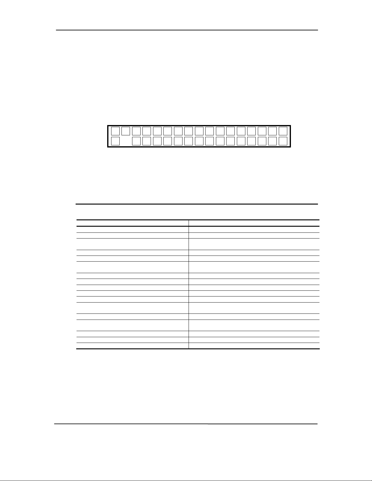
Technical Reference Guide
5.3.2 DISKETTE DRIVE CONNECTOR
This system uses a standard 34-pin connector (refer to Figure 5-2 and Table 5-6 for the pinout) for
diskette drives. Drive power is supplied through a separate connector.
1
6
4
2
5
10
8
9
7
Figure 5-2. 34-Pin Diskette Drive Connector.
Table 5–6. 34-Pin Diskette Drive Connector Pinout
34-Pin Diskette Drive Connector Pinout
SEL-
SEL-
SEL-
Description Pin Signal Description
Drive 4 select 23 GND Ground
Drive 2 select 29 GND Ground
Drive 1 select 31 GND Ground
Pin Signal
1 GND Ground 18 DIR- Drive head direction control
2 LOW DEN- Low density select 19 GND Ground
3 --- (KEY) 20 STEP- Drive head track step
4 MEDIA ID- Media identification 21 GND Ground
5 GND Ground 22 WR DATA- Write data
6 DRV 4
7 GND Ground 24 WR ENABLE- Enable for WR DATA8 INDEX- Media index is detected 25 GND Ground
9 GND Ground 26 TRK 00- Heads at track 00 indicator
10 MTR 1 ON- Activates drive motor 27 GND Ground
11 GND Ground 28 WR PRTK- Media write protect status
12 DRV 2
13 GND Ground 30 RD DATA- Data and clock read off disk
14 DRV 1
15 GND Ground 32 SIDE SEL- Head select (side 0 or 1)
16 MTR 2 ON- Activates drive motor 33 GND Ground
17 GND Ground 34 DSK CHG- Drive door opened indicator
14
12
13
11
20
18
16
19
17
15
Table 5-6.
22
21
23
25
27
29
control
31
33
34
32
30
28
26
24
Compaq D315 and hp d325 Personal Computers
5-7
Featuring the AMD Athlon XP Processor
Second Edition - April 2003
Page 90
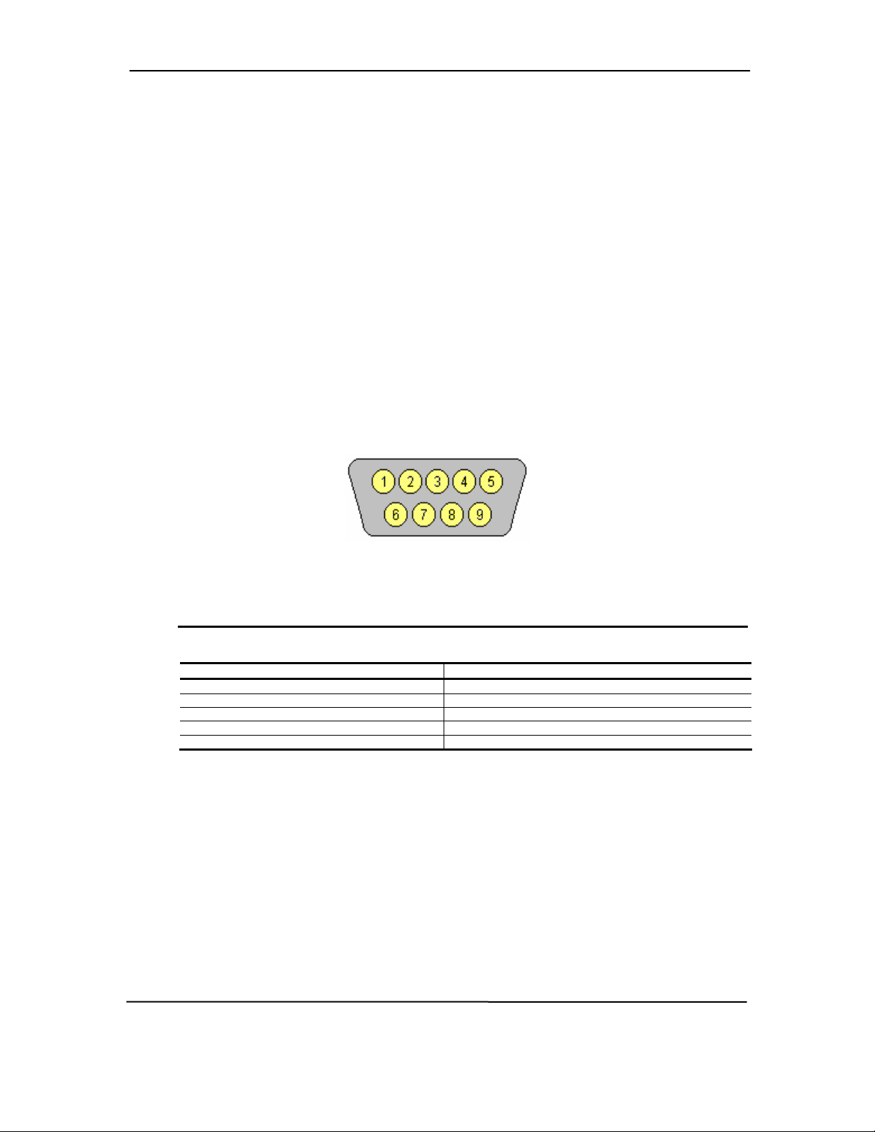
Chapter 5 Input/Output Interfaces
5.4 SERIAL INTERFACE
All models include at least one RS-232-C type serial interface to transmit and receive
asynchronous serial data with external devices. The serial interface function is provided by the
LPC47B367 I/O controller component that includes two NS16C550-compatible UARTs.
The UART supports the standard baud rates up through 115200, and also special high speed rates
of 239400 and 460800 baud. The baud rate of the UART is typically set to match the capability of
the connected device. While most baud rates may be set at runtime, baud rates 230400 and
460800 must be set during the configuration phase.
5.4.1 SERIAL CONNECTOR
The serial interface uses a DB-9 connector as shown in the following figure with the pinout listed
in Table 5-5.
Figure 5-3. Serial Interface Connector (Male DB-9 as viewed from rear of chassis)
Table 5–7. DB-9 Serial Connector Pinout
DB-9 Serial Connector Pinout
Pin Signal
1 CD Carrier Detect 6 DSR Data Set Ready
2 RX Data Receive Data 7 RTS Request To Send
3 TX Data Transmit Data 8 CTS Clear To Send
4 DTR Data Terminal Ready 9 RI Ring Indicator
5 GND Ground -- -- --
The standard RS-232-C limitation of 50 feet (or less) of cable between the DTE (computer) and
DCE (modem) should be followed to minimize transmission errors. Higher baud rates may require
shorter cables.
Description Pin Signal Description
Table 5-7.
5-8 Compaq D315 and hp d325 Personal Computers
Featuring the AMD Athlon XP Processor
Second Edition – April 2003
Page 91

Technical Reference Guide
5.4.2 SERIAL INTERFACE PROGRAMMING
Programming the serial interfaces consists of configuration, which occurs during POST, and
control, which occurs during runtime.
5.4.2.1 Serial Interface Configuration
The serial interface must be configured for a specific address range (COM1, COM2, etc.) and also
must be activated before it can be used. Address selection and activation of the serial interface are
affected through the PnP configuration registers of the LPC47B367 I/O controller.
The serial interface configuration registers are listed in the following table:
Table 5–8. Serial Interface Configuration Registers
Table 5-8.
Serial Interface Configuration Registers
Index
Address Function
30h Activate R/W
60h Base Address MSB R/W
61h Base Address LSB R/W
70h Interrupt Select R/W
F0h Mode Register R/W
NOTE:
Refer to LPC47B367 data sheet for detailed register information.
R/W
Compaq D315 and hp d325 Personal Computers
5-9
Featuring the AMD Athlon XP Processor
Second Edition - April 2003
Page 92

Chapter 5 Input/Output Interfaces
5.4.2.2 Serial Interface Control
The BIOS function INT 14 provides basic control of the serial interface. The serial interface can
be directly controlled by software through the I/O-mapped registers listed in Table 5-9.
Table 5–9. Serial Interface Control Registers
Serial Interface Control Registers
COM1
Addr.
3F8h 2F8h Receive Data Buffer
3F9h 2F9h Baud Rate Divisor Register 1 (when bit 7 of Line Control Reg. Is set)
3FAh 2FAh Interrupt ID Register
3FBh 2FBh Line Control Register R/W
3FCh 2FCh Modem Control Register R/W
3FDh 2FDh Line Status Register R
3FEh 2FEh Modem Status R
COM2
Addr.
Register
Transmit Data Buffer
Baud Rate Divisor Register 0 (when bit 7 of Line Control Reg. Is set)
Interrupt Enable Register
FIFO Control Register
Table 5-9.
R/W
R
W
W
W
R/W
R
W
5-10 Compaq D315 and hp d325 Personal Computers
Featuring the AMD Athlon XP Processor
Second Edition – April 2003
Page 93

Technical Reference Guide
5.5 PARALLEL INTERFACE
All models include a parallel interface for connection to a peripheral device that has a compatible
interface, the most common being a printer. The parallel interface function is integrated into the
LPC47B367 I/O controller component and provides bi-directional 8-bit parallel data transfers with
a peripheral device. The parallel interface supports three main modes of operation:
♦ Standard Parallel Port (SPP) mode
♦ Enhanced Parallel Port (EPP) mode
♦ Extended Capabilities Port (ECP) mode
These three modes (and their submodes) provide complete support as specified for an IEEE 1284
parallel port.
5.5.1 STANDARD PARALLEL PORT MODE
The Standard Parallel Port (SPP) mode uses software-based protocol and includes two sub-modes
of operation, compatible and extended, both of which can provide data transfers up to 150 KB/s.
In the compatible mode, CPU write data is simply presented on the eight data lines. A CPU read
of the parallel port yields the last data byte that was written.
The following steps define the standard procedure for communicating with a printing device:
1. The system checks the Printer Status register. If the Busy, Paper Out, or Printer Fault signals
are indicated as being active, the system either waits for a status change or generates an error
message.
2. The system sends a byte of data to the Printer Data register, then pulses the printer STROBE
signal (through the Printer Control register) for at least 500 ns.
3. The system then monitors the Printer Status register for acknowledgment of the data byte
before sending the next byte.
In extended mode, a direction control bit (CTR 37Ah, bit <5>) controls the latching of output data
while allowing a CPU read to fetch data present on the data lines, thereby providing bi-directional
parallel transfers to occur.
The SPP mode uses three registers for operation: the Data register (DTR), the Status register
(STR) and the Control register (CTR). Address decoding in SPP mode includes address lines A0
and A1.
Compaq D315 and hp d325 Personal Computers
5-11
Featuring the AMD Athlon XP Processor
Second Edition - April 2003
Page 94

Chapter 5 Input/Output Interfaces
5.5.2 ENHANCED PARALLEL PORT MODE
In Enhanced Parallel Port (EPP) mode, increased data transfers are possible (up to 2 MB/s) due to
a hardware protocol that provides automatic address and strobe generation. EPP revisions 1.7 and
1.9 are both supported. For the parallel interface to be initialized for EPP mode, a negotiation
phase is entered to detect whether or not the connected peripheral is compatible with EPP mode. If
compatible, then EPP mode can be used. In EPP mode, system timing is closely coupled to EPP
timing. A watchdog timer is used to prevent system lockup.
Five additional registers are available in EPP mode to handle 16- and 32-bit CPU accesses with
the parallel interface. Address decoding includes address lines A0, A1, and A2.
5.5.3 EXTENDED CAPABILITIES PORT MODE
The Extended Capabilities Port (ECP) mode, like EPP, also uses a hardware protocol-based
design that supports transfers up to 2 MB/s. Automatic generation of addresses and strobes as well
as Run Length Encoding (RLE) decompression is supported by ECP mode. The ECP mode
includes a bi-directional FIFO buffer that can be accessed by the CPU using DMA or programmed
I/O. For the parallel interface to be initialized for ECP mode, a negotiation phase is entered to
detect whether or not the connected peripheral is compatible with ECP mode. If compatible, then
ECP mode can be used.
Ten control registers are available in ECP mode to handle transfer operations. In accessing the
control registers, the base address is determined by address lines A2-A9, with lines A0, A1, and
A10 defining the offset address of the control register. Registers used for FIFO operations are
accessed at their base address + 400h (i.e., if configured for LPT1, then 378h + 400h = 778h).
The ECP mode includes several sub-modes as determined by the Extended Control register. Two
submodes of ECP allow the parallel port to be controlled by software. In these modes, the FIFO
is cleared and not used, and DMA and RLE are inhibited.
5-12 Compaq D315 and hp d325 Personal Computers
Featuring the AMD Athlon XP Processor
Second Edition – April 2003
Page 95

Technical Reference Guide
5.5.4 PARALLEL INTERFACE PROGRAMMING
Programming the parallel interface consists of configuration, which typically occurs during POST,
and control, which occurs during runtime.
5.5.4.1 Parallel Interface Configuration
The parallel interface must be configured for a specific address range (LPT1, LPT2, etc.) and also
must be enabled before it can be used. When configured for EPP or ECP mode, additional
considerations must be taken into account. Address selection, enabling, and EPP/ECP mode
parameters of the parallel interface are affected through the PnP configuration registers of the
LPC47B367 I/O controller. Address selection and enabling are automatically done by the BIOS
during POST but can also be accomplished with the Setup utility and other software.
The parallel interface configuration registers are listed in the following table:
Table 5–10. Parallel Interface Configuration Registers
Table 5-10.
Parallel Interface Configuration Registers
Index
Address Function
30h Activate R/W 00h
60h Base Address MSB R/W 00h
61h Base Address LSB R/W 00h
70h Interrupt Select R/W 00h
74h DMA Channel Select R/W 04h
F0h Mode Register R/W 00h
F1h Mode Register 2 R/W 00h
R/W
Reset
Value
Compaq D315 and hp d325 Personal Computers
5-13
Featuring the AMD Athlon XP Processor
Second Edition - April 2003
Page 96

Chapter 5 Input/Output Interfaces
5.5.4.2 Parallel Interface Control
The BIOS function INT 17 provides simplified control of the parallel interface. Basic functions
such as initialization, character printing, and printer status are provide by subfunctions of INT 17.
The parallel interface is controllable by software through a set of I/O mapped registers. The
number and type of registers available depends on the mode used (SPP, EPP, or ECP). Table 5-11
lists the parallel registers and associated functions based on mode.
Table 5–11. Parallel Interface Control Registers
Parallel Interface Control Registers
I/O
Address
Base Data LPT1,2,3 LPT1,2 LPT1,2,3
Base + 1h Printer Status LPT1,2,3 LPT1,2 LPT1,2,3
Base + 2h Control LPT1,2,3 LPT1,2 LPT1,2,3
Base + 3h Address -- LPT1,2 -Base + 4h Data Port 0 -- LPT1,2 -Base + 5h Data Port 1 -- LPT1,2 -Base + 6h Data Port 2 -- LPT1,2 -Base + 7h Data Port 3 -- LPT1,2 -Base + 400h Parallel Data FIFO -- -- LPT1,2,3
Base + 400h ECP Data FIFO -- -- LPT1,2,3
Base + 400h Test FIFO -- -- LPT1,2,3
Base + 400h Configuration Register A -- -- LPT1,2,3
Base + 401h Configuration Register B -- -- LPT1,2,3
Base + 402h Extended Control Register -- -- LPT1,2,3
Base Address:
LPT1 = 378h
LPT2 = 278h
LPT3 = 3BCh
Register
Table 5-11.
SPP
Mode
Ports
EPP
Mode
Ports
ECP
Mode
Ports
5-14 Compaq D315 and hp d325 Personal Computers
Featuring the AMD Athlon XP Processor
Second Edition – April 2003
Page 97

Technical Reference Guide
5.5.5 PARALLEL INTERFACE CONNECTOR
Figure 5-4 and Table 5-12 show the connector and pinout of the parallel interface connector. Note
that some signals are redefined depending on the port’s operational mode.
2 3 4 5 6 7 8 9
10 11 12 13
1
14 15 16 17 18 19 20 21 22 23 24 25
Figure 5-4. Parallel Interface Connector (Female DB-25 as viewed from rear of chassis)
Table 5–12. DB-25 Parallel Connector Pinout
Table 5-12.
DB-25 Parallel Connector Pinout
Pin Signal Function Pin Signal Function
1 STB- Strobe / Write [1] 14 LF- Line Feed [2]
2 D0 Data 0 15 ERR- Error [3]
3 D1 Data 1 16 INIT- Initialize Paper [4]
4 D2 Data 2 17 SLCTIN- Select In / Address. Strobe [1]
5 D3 Data 3 18 GND Ground
6 D4 Data 4 19 GND Ground
7 D5 Data 5 20 GND Ground
8 D6 Data 6 21 GND Ground
9 D7 Data 7 22 GND Ground
10 ACK- Acknowledge / Interrupt [1] 23 GND Ground
11 BSY Busy / Wait [1] 24 GND Ground
12 PE Paper End / User defined [1] 25 GND Ground
13 SLCT Select / User defined [1] -- -- --
NOTES:
[1] Standard and ECP mode function / EPP mode function
[2] EPP mode function: Data Strobe
ECP modes: Auto Feed or Host Acknowledge
[3] EPP mode: user defined
ECP modes:Fault or Peripheral Req.
[4] EPP mode: Reset
ECP modes: Initialize or Reverse Req.
Compaq D315 and hp d325 Personal Computers
5-15
Featuring the AMD Athlon XP Processor
Second Edition - April 2003
Page 98

Chapter 5 Input/Output Interfaces
5.6 KEYBOARD/POINTING DEVICE INTERFACE
The keyboard/pointing device interface function is provided by the LPC47B367 I/O controller
component, which integrates 8042-compatible keyboard controller logic (hereafter referred to as
simply the “8042”) to communicate with the keyboard and pointing device using bi-directional
serial data transfers. The 8042 handles scan code translation and password lock protection for the
keyboard as well as communications with the pointing device. This section describes the interface
itself. The keyboard is discussed in the Appendix C.
5.6.1 KEYBOARD INTERFACE OPERATION
The data/clock link between the 8042 and the keyboard is uni-directional for Keyboard Mode 1
and bi-directional for Keyboard Modes 2 and 3. (These modes are discussed in detail in Appendix
C). This section describes Mode 2 (the default) mode of operation.
Communication between the keyboard and the 8042 consists of commands (originated by either
the keyboard or the 8042) and scan codes from the keyboard. A command can request an action or
indicate status. The keyboard interface uses IRQ1 to get the attention of the CPU.
The 8042 can send a command to the keyboard at any time. When the 8042 wants to send a
command, the 8042 clamps the clock signal from the keyboard for a minimum of 60 us. If the
keyboard is transmitting data at that time, the transmission is allowed to finish. When the 8042 is
ready to transmit to the keyboard, the 8042 pulls the data line low, causing the keyboard to
respond by pulling the clock line low as well, allowing the start bit to be clocked out of the 8042.
The data is then transferred serially, LSb first, to the keyboard (Figure 5-5). An odd parity bit is
sent following the eighth data bit. After the parity bit is received, the keyboard pulls the data line
low and clocks this condition to the 8042. When the keyboard receives the stop bit, the clock line
is pulled low to inhibit the keyboard and allow it to process the data.
Start
Bit
(LSb)
0
Data
Clock
Th
Parameter
Tsh (Stop Bit Hold) 15 µs 25 µs
Figure 5-5. 8042-To-Keyboard Transmission of Code EDh, Timing Diagram
D0
1
D1
D2
D3
D4
0
1
Tcy
Tcy (Cycle Time) 0 µs 80 µs
Tcl (Clock Low) 25 µs 35 µs
Tch (Clock High) 25 µs 45 µs
Th (Data Hold) 0 µs 25 µs
Tss (Stop Bit Setup) 8 µs 20 µs
Tcl
1
Tch
0
Minimum
D5
1
Maximum
D6
D7
(MSb)
1
Parity
1
Stop
Bit
0
Tss
Tsh
1
5-16 Compaq D315 and hp d325 Personal Computers
Featuring the AMD Athlon XP Processor
Second Edition – April 2003
Page 99

Technical Reference Guide
Control of the data and clock signals is shared by the 8042 and the keyboard depending on the
originator of the transferred data. Note that the clock signal is always generated by the keyboard.
After the keyboard receives a command from the 8042, the keyboard returns an ACK code. If a
parity error or timeout occurs, a Resend command is sent to the 8042.
Table 5-13 lists and describes commands that can be issued by the 8042 to the keyboard.
Table 5–13. 8042-To-Keyboard Commands
Table 5-13.
8042-To-Keyboard Commands
Command
Set/Reset Status Indicators EDh Enables LED indicators. Value EDh is followed by an
Echo EEh Keyboard returns EEh when previously enabled.
Invalid Command EFh/F1h These commands are not acknowledged.
Select Alternate Scan Codes F0h Instructs the keyboard to select another set of scan codes
Read ID F2h Instructs the keyboard to stop scanning and return two
Set Typematic Rate/Display F3h Instructs the keyboard to change typematic rate and delay
Enable F4h Instructs keyboard to clear output buffer and last typematic
Default Disable F5h Resets keyboard to power-on default state and halts
Set Default F6h Resets keyboard to power-on default state and enable
Set Keys - Typematic F7h Clears keyboard buffer and sets default scan code set. [1]
Set Keys - Make/Brake F8h Clears keyboard buffer and sets default scan code set. [1]
Set Keys - Make F9h Clears keyboard buffer and sets default scan code set. [1]
Set Keys - Typematic/Make/Brake FAh Clears keyboard buffer and sets default scan code set. [1]
Set Type Key - Typematic FBh Clears keyboard buffer and prepares to receive key ID. [1]
Set Type Key - Make/Brake FCh Clears keyboard buffer and prepares to receive key ID. [1]
Set Type Key - Make FDh Clears keyboard buffer and prepares to receive key ID. [1]
Resend FEh 8042 detected error in keyboard transmission.
Reset FFh Resets program, runs keyboard BAT, defaults to Mode 2.
Note:
[1] Used in Mode 3 only.
Value Description
option byte that specifies the indicator as follows:
Bits <7..3> not used
Bit <2>, Caps Lock (0 = off, 1 = on)
Bit <1>, NUM Lock (0 = off, 1 = on)
Bit <0>, Scroll Lock (0 = off, 1 = on)
and sends an option byte after ACK is received:
01h = Mode 1
02h = Mode 2
03h = Mode 3
keyboard ID bytes.
to specified values:
Bit <7>, Reserved - 0
Bits <6,5>, Delay Time
00 = 250 ms
01 = 500 ms
10 = 750 ms
11 = 1000 ms
Bits <4..0>, Transmission Rate:
00000 = 30.0 ms
00001 = 26.6 ms
00010 = 24.0 ms
00011 = 21.8 ms
:
11111 = 2.0 ms
key and begin key scanning.
scanning pending next 8042 command.
scanning.
Compaq D315 and hp d325 Personal Computers
5-17
Featuring the AMD Athlon XP Processor
Second Edition - April 2003
Page 100

Chapter 5 Input/Output Interfaces
5.6.2 POINTING DEVICE INTERFACE OPERATION
The pointing device (typically a mouse) connects to a 6-pin DIN-type connector that is identical to
the keyboard connector both physically and electrically. The operation of the interface (clock and
data signal control) is the same as for the keyboard. The pointing device interface uses the IRQ12
interrupt.
5.6.3 KEYBOARD/POINTING DEVICE INTERFACE PROGRAMMING
Programming the keyboard interface consists of configuration, which occurs during POST, and
control, which occurs during runtime.
5.6.3.1 8042 Configuration
The keyboard/pointing device interface must be enabled and configured for a particular speed
before it can be used. Enabling and speed parameters of the 8042 logic are affected through the
PnP configuration registers of the LPC47B367 I/O controller. Enabling and speed control are
automatically set by the BIOS during POST but can also be accomplished with the Setup utility
and other software.
The keyboard interface configuration registers are listed in the following table:
Table 5–14. Keyboard Interface Configuration Registers
Table 5-14.
Keyboard Interface Configuration Registers
Index
Address Function
30h Activate R/W
70h Primary Interrupt Select R/W
72h Secondary Interrupt Select R/W
F0h Reset and A20 Select R/W
5-18 Compaq D315 and hp d325 Personal Computers
Featuring the AMD Athlon XP Processor
Second Edition – April 2003
R/W
 Loading...