

2 – 16 GHz General Purpose
Gallium Arsenide FET
Technical Data
ATF-26884
Features
• High Output Power:
18.0␣ dBm Typical P
• High Gain:
9.0 dB Typical GSS at 12␣ GHz
• Low Cost Plastic Package
• Tape-and-Reel Packaging
Option Available
at 12␣ GHz
1 dB
[1]
Description
The ATF-26884 is a high performance gallium arsenide Schottkybarrier-gate field effect transistor
Electrical Specifications, T
Symbol Parameters and Test Conditions Units Min. Typ. Max.
G
SS
NF
G
A
P
1 dB
g
m
I
DSS
V
P
Note:
1. Refer to PACKAGING section “Tape-and-Reel Packaging for Surface Mount Semiconductors.”
Tuned Small Signal Gain: VDS = 5 V, IDS = 30 mA f = 12.0 GHz dB 7.0 9.0
Optimum Noise Figure: VDS = 3 V, IDS = 10 mA f = 12.0 GHz dB 2.2
O
Gain @ NFO: VDS = 3 V, IDS = 10 mA f = 12.0 GHz dB 6.0
Power Output @ 1 dB Gain Compression: f = 12.0 GHz dB m 15.0 18.0
VDS = 5 V, IDS = 30 mA
Transconductance: VDS = 3 V, VGS = 0 V mmho 15 35
Saturated Drain Current: VDS = 3 V, VGS = 0 V mA 30 50 90
Pinch-off Voltage: VDS = 3 V, IDS = 1 mA V -3.5 -1.5 -0.5
housed in a cost effective
microstrip package. This device is
designed for use in oscillator
applications and general purpose
amplifier applications in the
2-16␣ GHz frequency range.
This GaAs FET device has a
nominal 0.3 micron gate length
with a total gate periphery of
250␣ microns. Proven gold based
metallization systems and nitride
passivation assure a rugged,
reliable device.
= 25° C
A
84 Plastic Package
5-71
5965-8703E
ATF-26884 Absolute Maximum Ratings
Absolute
Symbol Parameter Units Maximum
V
DS
V
GS
V
GD
I
DS
P
T
T
CH
T
STG
Thermal Resistance: θjc = 300°C/W; T
Liquid Crystal Measurement: 1␣ µm Spot Size
Drain-Source Voltage V +7
Gate-Source Voltage V -4
Gate-Drain Voltage V -8
Drain Current mA I
Power Dissipation
[2,3]
m W 275
Channel Temperature ° C 175
Storage Temperature °C -65 to +150
= 150°C
CH
[4]
Part Number Ordering Information
Part Number Devices Per Reel Reel Size
ATF-26884-TR1 1000 7"
ATF-26884-STR 10 strip
DSS
[1]
Notes:
1. Permanent damage may occur if
any of these limits are exceeded.
2. T
CASE TEMPERATURE
= 25°C.
3. Derate at 3.3 mW/°C for
> 92.5°C.
T
CASE
4. The small spot size of this technique results in a higher, though
more accurate determination of θ
than do alternate methods. See
MEASUREMENTS section for
more information.
jc
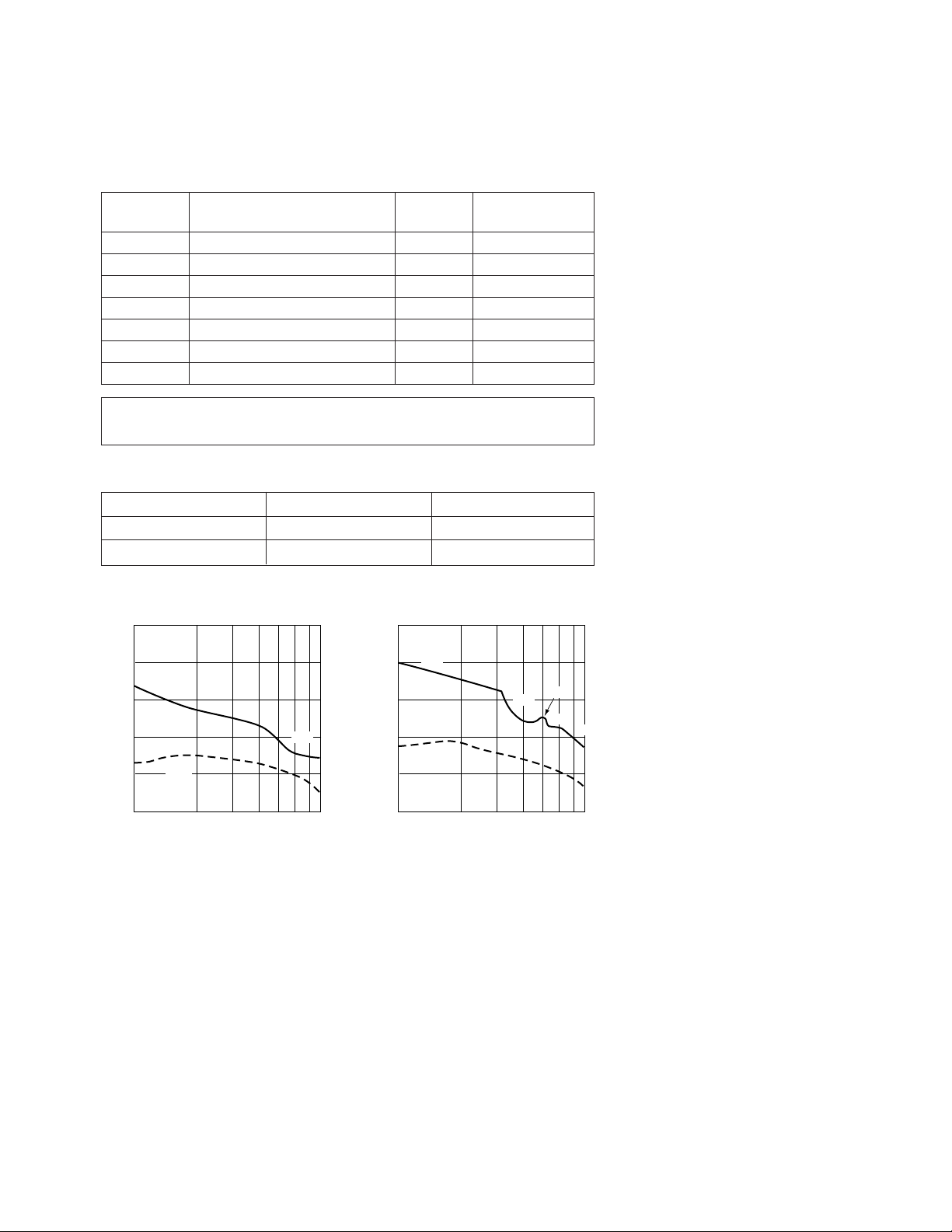
ATF-26884 Typical Performance, T
25
20
15
10
GAIN (dB)
Figure 1. Insertion Power Gain,
Maximum Available Gain and
Maximum Stable Gain vs. Frequency.
VDS = 3 V, IDS = 10 mA.
MSG
2
|S21|
5
0
2.0 4.0 6.0 8.0
FREQUENCY (GHz)
MAG
10.0 12.0 16.0
25
20
15
10
GAIN (dB)
5
0
2.0 4.0 6.0 8.0
Figure 2. Insertion Power Gain,
Maximum Available Gain and
Maximum Stable Gain vs. Frequency.
VDS = 5 V, IDS = 30 mA.
= 25° C
A
MSG
2
|S21|
FREQUENCY (GHz)
MAG
10.0 12.0 16.0
MSG
MAG
MSG
5-72

Typical Scattering Parameters, Common Emitter, Z
Freq. S
11
S
21
= 50 Ω, TA=25°C, V
O
S
12
=3 V, I
DS
=␣ 10 mA
DS␣
S
GHz Mag. Ang. dB Mag. Ang. dB Mag. Ang. Mag. Ang.
2.0 .96 -36 6.9 2.21 142 -26.6 .047 64 .81 -25
3.0 .91 -56 7.4 2.35 123 -23.0 .071 50 .77 -38
4.0 .86 -78 7.6 2.39 103 -20.6 .093 36 .70 -50
5.0 .79 -97 7.2 2.30 86 -19.5 .106 25 .66 -61
6.0 .73 -113 6.8 2.20 71 -18.9 .114 16 .62 -70
7.0 .67 -127 6.4 2.10 56 -18.4 .120 9 .61 -78
8.0 .62 -144 6.4 2.08 41 -17.9 .128 1 .58 -88
9.0 .57 -168 6.2 2.03 23 -17.5 .134 -8 .54 -101
10.0 .53 168 5.8 1.96 6 -17.3 .136 -16 .47 -116
11.0 .52 147 5.2 1.81 -10 -17.2 .138 -22 .41 -133
12.0 .49 124 4.9 1.76 -22 -17.1 .140 -26 .39 -143
13.0 .52 103 4.6 1.70 -36 -16.7 .146 -31 .37 -154
14.0 .56 80 4.0 1.58 -54 -16.3 .153 -37 .35 -171
15.0 .60 65 3.3 1.46 -72 -16.3 .153 -42 .35 173
16.0 .65 52 2.9 1.40 -83 -16.3 .153 -48 .37 132
17.0 .68 40 2.3 1.30 -99 -16.0 .158 -56 .41 101
18.0 .69 30 1.3 1.16 -112 -15.9 .159 -72 .47 87
22
Typical Scattering Parameters, Common Emitter, Z
Freq. S
11
S
21
= 50 Ω, TA=25°C, V
O
S
12
=5 V, I
DS
=␣ 30 mA
DS␣
S
GHz Mag. Ang. dB Mag. Ang. dB Mag. Ang. Mag. Ang.
2.0 .94 -41 9.2 2.88 138 -30.8 .029 65 .84 -23
3.0 .87 -65 9.5 2.97 118 -27.3 .043 51 .80 -34
4.0 .79 -89 9.3 2.93 97 -25.5 .053 40 .74 -44
5.0 .71 -109 8.7 2.73 79 -24.9 .057 35 .71 -53
6.0 .64 -126 8.1 2.54 64 -24.4 .060 33 .69 -60
7.0 .57 -142 7.5 2.38 50 -24.0 .063 31 .69 -67
8.0 .52 -162 7.2 2.30 35 -23.1 .070 30 .69 -76
9.0 .48 174 6.9 2.21 18 -21.9 .080 28 .67 -87
10.0 .48 149 6.5 2.11 1 -20.4 .095 24 .63 -100
11.0 .48 130 5.9 1.97 -14 -19.7 .104 22 .57 -114
12.0 .49 108 5.6 1.91 -25 -18.1 .125 20 .55 -122
13.0 .53 88 5.2 1.82 -39 -16.2 .155 18 .54 -132
14.0 .57 69 4.7 1.71 -55 -15.2 .173 5 .52 -146
15.0 .62 56 4.1 1.60 -75 -14.8 .182 -1 .52 -165
16.0 .70 44 3.7 1.53 -87 -13.8 .205 -16 .52 165
17.0 .75 33 3.0 1.41 -103 -12.9 .226 -28 .54 135
18.0 .74 24 2.3 1.30 -117 -13.6 .210 -44 .63 114
A model for this device is available in the DEVICE MODELS section.
22
5-73

84 Plastic Package Dimensions
0.51 (0.020)
4
SOURCE
1.52 ± 0.25
(0.060 ± 0.010)
268
SOURCE
DRAIN
3
0.20 ± 0.050
(0.008 ± 0.002)
GATE
1
2
2.15
(0.085)
5°
5.46 ± 0.25
0.51
(0.020)
DIMENSIONS ARE IN MILLIMETERS (INCHES)
(0.215 ± 0.010)
5-74
 Loading...