0.5 –6 GHz General Purpose
Gallium Arsenide FET
Technical Data
ATF-21186
Features
• Low Noise Figure:
0.5 dB Typ. @ 2 GHz
• High Output Power:
19 dBm Typ. P
• High MSG:
13.5 dB Typ. @ 2 GHz
• Low Cost Surface Mount
Plastic Package
• Tape-and-Reel Packaging
Option Available
Note:
1. Refer to “Tape-and-Reel Packaging for
Surface Mount Semiconductors”.
30
20
GAIN (dB)
10
0
0.1
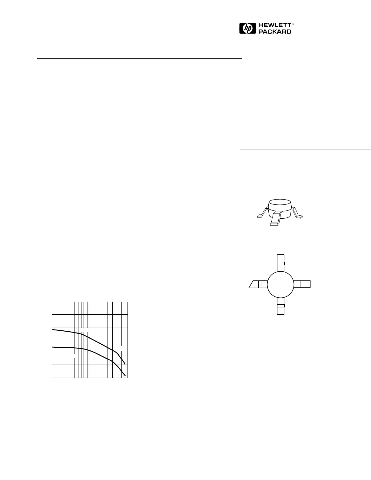
ATF-21186 Insertion Power Gain,
Maximum Available Gain, and
Maximum Stable Gain vs. Frequency.
V
= 2 V, IDS = 15 mA.
DS
S
21
@ 2 GHz
1dB
[1]
MSG
FREQUENCY (GHz)
MAG
Description
Hewlett–Packard’s ATF-21186 is a
low cost Gallium Arsenide
Schottky barrier-gate field effect
transistor housed in a surface
mount plastic package. This
general purpose device is
designed for use in low noise
amplifiers, gain stages, driver
amplifiers, and oscillators
operating over the VHF, UHF, and
microwave frequency ranges.
High gain with two volt operation
makes this part attractive for low
voltage, battery operated systems.
The low noise figure is
appropriate for commercial
systems demanding good
sensitivity, such as GPS receiver
front-ends and MMDS television
receivers. The output power is
sufficient for use as the driver
stage in many hand-held
transceivers operating in the
900␣ MHz through 2.4 GHz bands,
including in cellular phones, PCN,
and ISM band spread spectrum
101
applications.
85 mil Plastic Surface Mount Package
Pin Configuration
4
SOURCE
DRAINGATE
1
211
2 SOURCE
This GaAs FET device has a
nominal 0.3 micron gate length
using airbridge interconnects
between drain fingers. Total gate
periphery is 750 microns. Proven
gold based metallization systems
and nitride passivation assure a
rugged, reliable device.
3
5-49
5965-8716E

ATF-21186 Absolute Maximum Ratings
Symbol Parameter Units Absolute Maximum
V
DS
V
GS
V
GD
I
DS
P
T
T
CH
T
STG
Drain-Source Voltage V 5
Gate-Source Voltage V -4
Gate-Drain Voltage V -6
Drain Current mA I
Power Dissipation
[2,3]
m W 400
DSS
Channel Temperature ° C 150
Storage Temperature °C -65 to +150
Notes:
[1]
1. Operation of this device above any
one of these parameters may cause
permanent damage.
2. T
3. Derate at 4.4 mW/oC for TC␣>␣ 60oC.
= 25oC (T
CASE
be the temperature at the ends of
pins 2 and 4 where they contact the
circuit board).
CASE
is defined to
Thermal Resistance
ATF-21186 Electrical Specifications, T
[2]
: θjc = 225° C/W
= 25°C
A
Symbol Parameters and Test Conditions Units Min. Typ. Max.
NF
o
Optimum Noise Figure f = 1 GHz dB 0.4
VDS = 2 V, IDS = 15 mA f = 2 GH z 0.5 0.75
f = 4 GHz 0.6
G
A
Associated Gain f = 1 GHz dB 14.2
VDS = 2 V, IDS = 15 mA f = 2 GH z 12.0 12.6
f = 4 GHz 9.1
P
1 dB
Power at 1 dB Gain Compression f = 1 GHz dBm 19.0
VDS = 3 V, IDS = 70 mA f = 2 GH z 19.0
f = 4 GHz 18.0
G
1 dB
1 dB Compressed Gain f = 1 GHz dB 18.0
VDS = 3 V, IDS = 70 mA f = 2 GH z 14.0
f = 4 GHz 8.5
I
g
DSS
V
m
P
Transconductance VDS = 3 V, VGS = 0 V mS 70 120
Saturated Drain Current VDS = 3 V, VGS = 0 V m A 80 120 200
Pinchoff Voltage VDS = 3 V, IDS = 1 mA V -3.0 -1.5 -0.8
5-50

ATF-21186 Typical Performance, T
1.5
G
A
1.0
O
NF (dB)
0.5
10 mA
15 mA
20 mA
0
0.1
FREQUENCY (GHz)
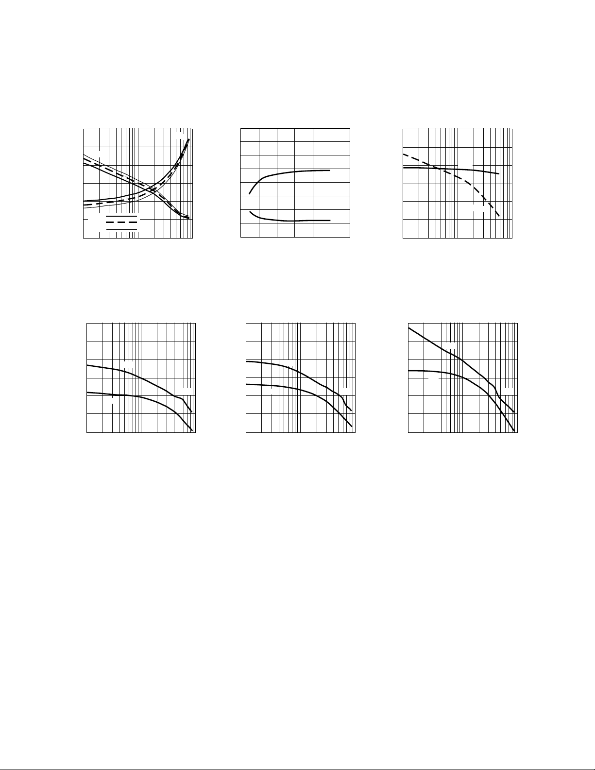
Figure 1. ATF-21186 Optimum Noise
Figure and Associated Gain vs.
Frequency and IDS, VDS = 2 V.
30
NF
O
20
2.0
A
G (dB)
10
0
101
1.5
1.0
NF (dB)
0.5
0
0
Figure 2. ATF-21186 Optimum Noise
Figure and Associated Gain vs. IDS,
f␣ =␣ 2 GHz, VDS = 2 V.
= 25° C
A
NF
I (mA)
DS
20
18
G
A
16
14
12
6010
50403020
A
G (dB)
30
20
1 dB
P (dBm)
10
0
0.1
P
1 dB
FREQUENCY (GHz)
30
20
1 dB
G (dB)
G
1 dB
10
0
101
Figure 3. ATF-21186 Power Output at
1 dB Compression and 1 dB
Compressed Gain vs. Frequency.
VDS␣=␣3 V, IDS = 70 mA.
30
20
GAIN (dB)
10
0
0.1
MSG
S
21
FREQUENCY (GHz)
MAG
101
Figure 4. ATF-21186 Insertion Power
Gain, Maximum Available Gain, and
Maximum Stable Gain vs. Frequency.
VDS = 2 V, IDS = 10 mA.
30
20
GAIN (dB)
10
0
0.1
MSG
S
21
FREQUENCY (GHz)
MAG
101
Figure 5. ATF-21186 Insertion Power
Gain, Maximum Available Gain, and
Maximum Stable Gain vs. Frequency.
VDS = 2 V, IDS = 20 mA.
30
MSG
20
S
GAIN (dB)
10
0
21
MAG
0.1
FREQUENCY (GHz)
101
Figure 6. ATF-21186 Insertion Power
Gain, Maximum Available Gain, and
Maximum Stable Gain vs. Frequency.
VDS = 3 V, IDS = 70 mA.
5-51
 Loading...