

Page 1

HP 8970B Option 020
Service Manual
Supplement
Page 2

Page 3

Service Manual Supplement
HP 8970B Option 020
HP Part no. 08970-90115
Edition 1
May 1998
Page 4

UNIX is a registered trademark of AT&T in the USA and other countries.OSF/Motif is a
trademark of the Open Software Foundation, Inc. in the USA and other countries.
© Copyright Hewlett-Packard Company May 1998
All rights reserved. Reproduction, adaptation, or translation without prior written
permission is prohibited, except as allowed under the copyright laws.
Printed in the UK.
ii HP 8970B Option 020 Service Manual Supplement
Page 5
Printing History
Printing History
Date
May 1998 1 08970-90115
Manual
Edition
Notes
HP 8970B Option 020 Service Manual Supplement iii
Page 6

List of Related Publications
List of Related Publications
HP Part Number Title
08970-90054 HP 8970B Noise Figure Meter Service Manual
About this Manual
This document is a supplement to the HP 8970B Noise Figure Meter Service Manual
(08970-90054) and provides information useful for operating the HP 8970B Option 020. It
also gives some troubleshooting tips.
iv HP 8970B Option 020 Service Manual Supplement
Page 7

Table of Contents
Page
Printing History.....................................................................................................iii
List of Related Publications .................................................................................. iv
About this Manual................................................................................................. iv
Block Diagram and Parts List.................................................................................... 1-1
Block Diagram......................................................................................................... 1-2
Front End ................................................................................................................1-3
Material List ........................................................................................................... 1-5
Theory of Operation..................................................................................................... 2-1
General.................................................................................................................... 2-2
Adjustments.................................................................................................................... 3-1
General.................................................................................................................... 3-2
Input power detector Gain and Offset Adjustment............................................... 3-2
600 MHz SAW Oscillator Frequency Adjustment................................................. 3-3
Board Differences .........................................................................................................4-1
General.................................................................................................................... 4-2
Microprocessor Board ............................................................................................. 4-2
20 MHz IF Assembly (08970-60050)......................................................................4-3
Driver Assembly (08970-60089)............................................................................. 4-4
Fault-Finding Tips........................................................................................................5-1
General.................................................................................................................... 5-2
Filter (0955-0634) ................................................................................................... 5-2
Input Assembly (08970-60097 or 08970-60125)....................................................5-3
YIG Tuned Oscillator (0955-0630)......................................................................... 5-4
Mixer (0955-0635)................................................................................................... 5-4
Isolator (0960-0638)................................................................................................ 5-5
4.5 GHz Low Pass Filter (9135-0169).................................................................... 5-5
Second Convertor (5086-7909) ............................................................................... 5-6
600 MHz SAW Oscillator (08970-60093)............................................................... 5-6
Board Details.................................................................................................................. 6-1
Page 8

Contents-2 HP 8970B Option 020 Service Manual Supplement
Page 9

1
Block Diagram and Parts List
Page 10
Block Diagram and Parts List
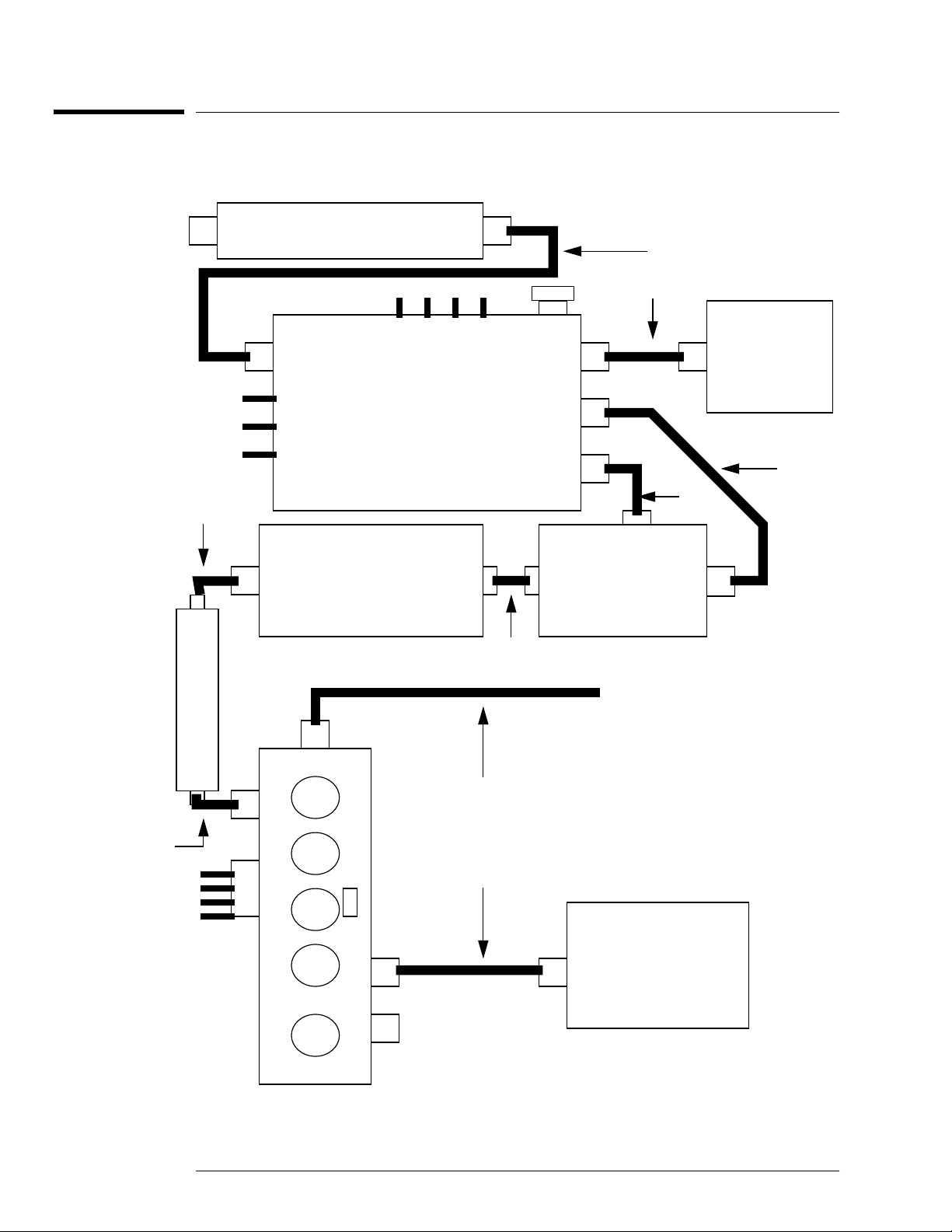
Block Diagram
Block Diagram
Figure 1-1: HP 8970B Option 020 Front End Schematic
2.05 GHz Low Pass Filter
W1
PAD 1
PAD 2
PAD 3
W6
4.5 GHz LPF
O/P
J1
(924)
(925)
(926)
ISOLATOR
J2
+15 V (2)
20 dB AMP (923)
DETECTOR (927)
INPUT ASSEMBLY
I/P
-15 V (7)
W5
W8
J4
RF
J3
J5
J2
50 Ω
MIXER
W2
IF
TO A4 ASSEMBLY
4 - 6 GHz
Y.T.O
W3
W4
LO
J1
W7
92
0
92
2
J4 J3
J5
Second Convertor
1-2 HP 8970B Option 020 Service Manual Supplement
LO MONITOR
W9
600 MHz SAW
Oscillator
Page 11
Front End
Block Diagram and Parts List
Front End
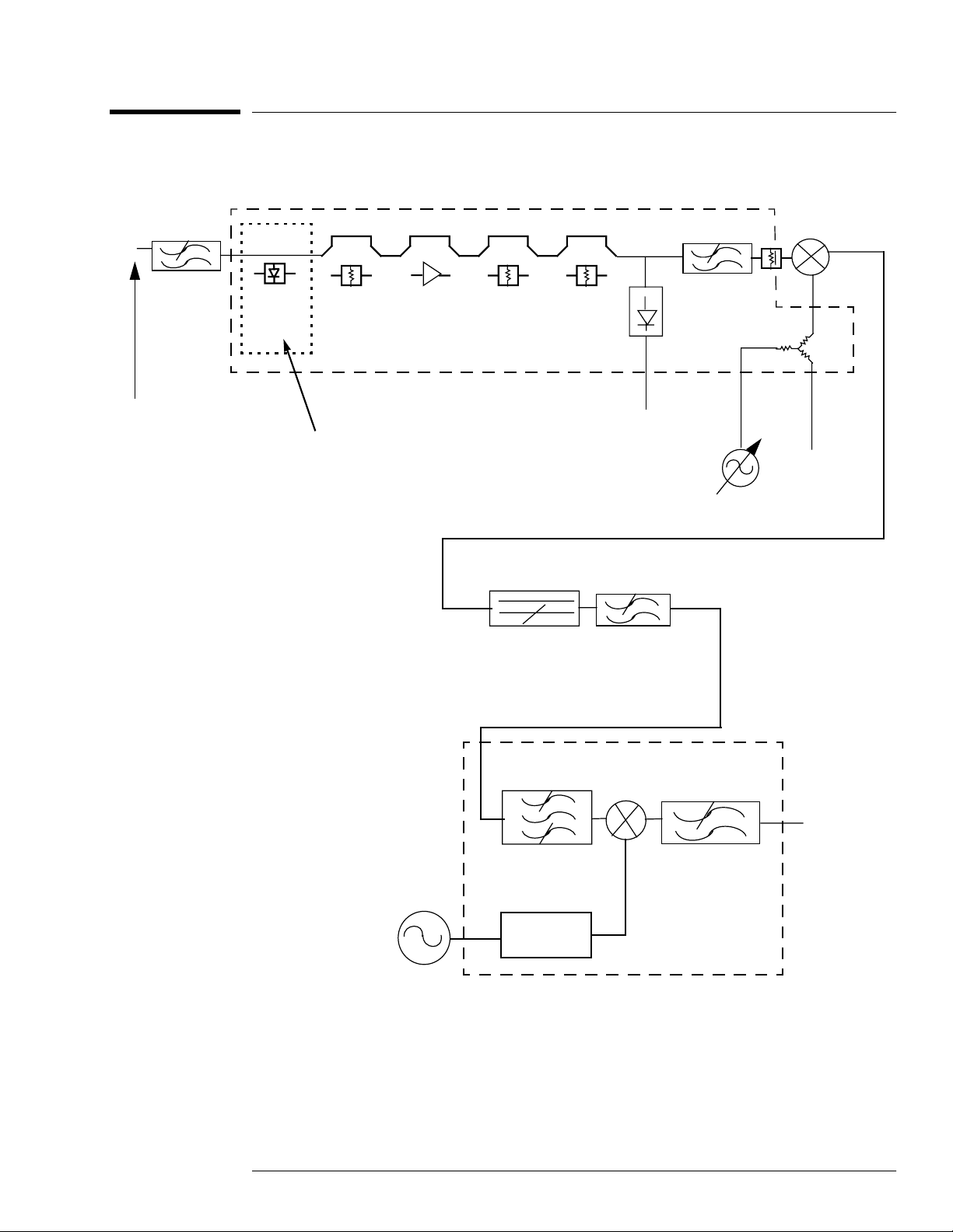
Figure 1-2: HP 8970B Front End Schematic
2050 MHz LPF
J1
10 - 2047 MHz
Limiter
10 dB
20 dB
INPUT ASSEMBLY
Limiter (on 08970-60125
Input Assembly only).
Suppresses externally
generated transients.
10 dB
2-7 GHz Isolator
10 dB
Detector
Diode
Output
4.5 GHz LPF
2 dB
J3
YTO Output
3.910 - 5.947 GHz
J2
J5
J4
600 MHz
3.9 GHz
300 MHz
To A4 Assy
3.6 GHz
X 6
2nd Convertor
HP 8970B Option 020 Service Manual Supplement 1-3
Page 12
Block Diagram and Parts List
Front End
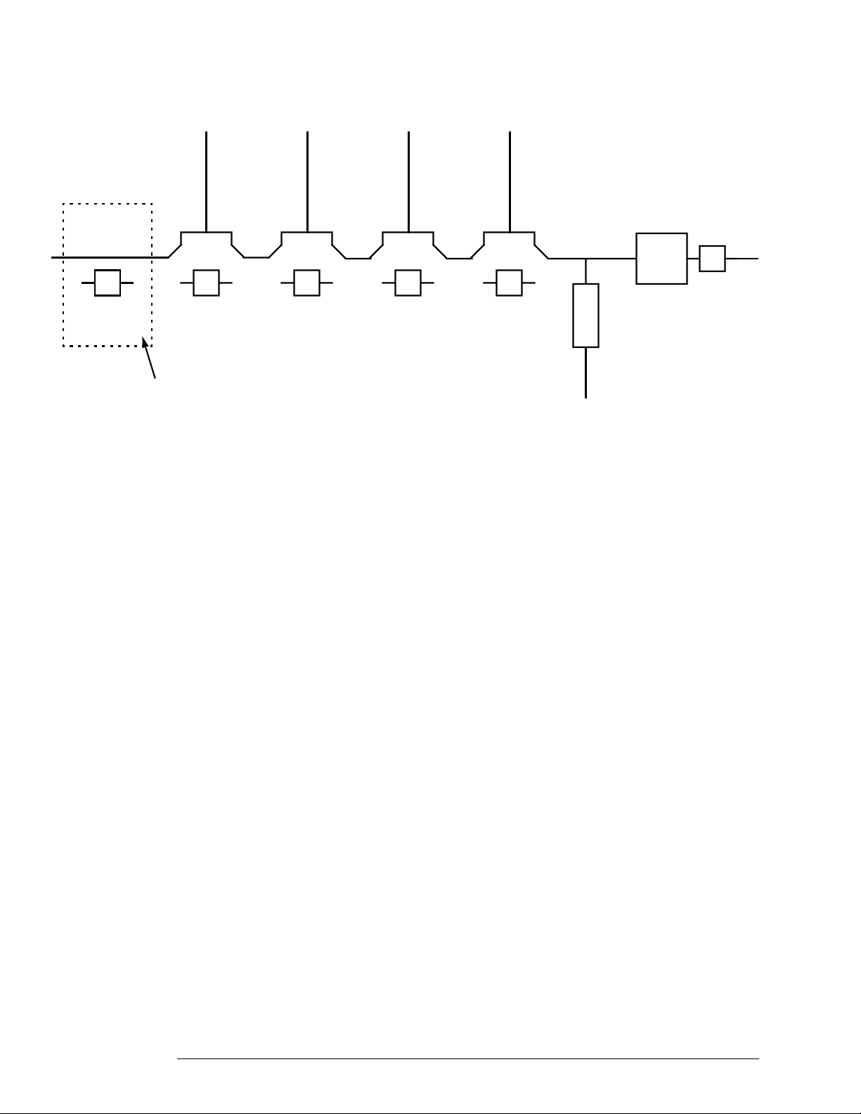
Figure 1-3: Schematic Representation of Input Assembly
PAD 1 20 dB
Limiter
10 dB
PAD
Limiter (on 08970-60125
Input Assembly only).
This is a schematic representation of the RF input assembly. The amplifier section and
each and each of the attenuator sections are switchable by the control lines.
On units using the Input Assembly 08970-60125, the Limiter suppresses externally
generated transients.
In Figure 1-1 the numbers in brackets inside the input assembly refer to the wire colors.
The numbers at the side of the second convertor refer to the wire colors attached to the
connector which connects up to the second convertor.
20 dB
AMP
Amp
PAD 2 PAD 3
10 dB
PAD
10 dB
PAD
Detector
3 GHz
LPF
2dB
PAD
1-4 HP 8970B Option 020 Service Manual Supplement
Page 13

Block Diagram and Parts List
Material List
Material List
Table 1-1: HP 8970B Option 020 Material List - main differences for Option 020
Description Part Number Quantity
2.05 GHz Low Pass Filter 0955-0634 1
Semi-rigid cable W1 08970-20082 1
Input Assembly 08970-60097 1
Input Assembly 08970-60125
2 to 8 GHz YIG Tuned Oscillator 0955-0630 1
YIG Tuned Oscillator Interface Board 08970-60045 1
YIG Tuned Oscillator Shield 08590-00047 1
Semi-rigid cable W2 08970-20081 1
1
1
Semi-rigid cable W3 08970-20083 1
Semi-rigid cable W4 08970-20085 1
Microwave Mixer 0955-0635 1
Semi-rigid cable W5 08970-20084 1
Microwave Isolator 0960-0638 1
Right Angle SMA(F) to SMA (M) Adapter W6 1250-1249 1
4.5 GHz Low Pass Filter 9135-0169 1
SMA(M) to SMA (M) Adapter W7 1250-2189 1
Second Convertor 5086-7909 1
600 MHz SAW Oscillator 08970-60093 1
Flexi Cable W8 83711-60035 1
Flexi Cable W9 83711-60035 1
Main Wiring Harness 08970-60046
Firmware EPROM’s 08970-80071/72
20 MHz IF Assembly 08970-60050
Driver Board Assembly 08970-60089
2
3
4
5
1
2
1
1
SMA (M) 50 Ω Termination 0960-0053 1
1. Replaces 08970-60097 from prefix break 3811.
2. This is the same part number as the main instrument but different wires are used. The wires
that are not used are tied back.
3. These replace 08970-80051/52
4. Replaces 08970-60003
5. Replaces 08970-60034
HP 8970B Option 020 Service Manual Supplement 1-5
Page 14

Block Diagram and Parts List
Material List
1-6 HP 8970B Option 020 Service Manual Supplement
Page 15

2
Theory of Operation
Page 16

Theory of Operation
General
General
The input range of the instrument is 10 MHz to 2047 MHz.
The input signal is first low pass filtered, using the 2050 MHz filter, to avoid images.
The YIG tuned oscillator tunes over the range 3910 MHz to 5947 MHz to mix the
incoming signal to a first IF of 3900 MHz.
The isolator ensures that any rejected signals are absorbed in the isolator and do not
interfere with the front end detector circuitry.
The second convertor mixes 3900 MHz down to 300 MHz. There is a cavity tuned
bandpass filter which is tuned for 3900 MHz. This is set at the factory and should not be
adjusted. The LO input is 600 MHz, but this is multiplied up to 3600 MHz by a X6 circuit.
The 3600 MHz can be monitored at the LO Monitor port.
The 600 MHz supplied to the second convertor comes from a 600 MHz SAW Oscillator.
The frequency is adjusted for 600 MHz ± 50 KHz. The power should be > -3 dBm.
2-2 HP 8970B Option 020 Service Manual Supplement
Page 17

3
Adjustments
Page 18

Adjustments
General
General
There are 2 adjustments that need to be made:
1. Input power detector gain and offset.
2. The 600 MHz SAW oscillator frequency adjustment.
Input power detector Gain and Offset Adjustment
Follow the adjustment procedure in section 5-13 of the Adjustments Chapter in the 8970B
Service Manual with the following exceptions.
Figure 3-1: Input detector gain and offset adjustment
RF Input
Assembly
R26
1. The input level must be -21 dBm ± 0.1 dB.
2. R32 is the offset adjustment.
3. R26 is the gain adjustment.
J1
R32
3-2 HP 8970B Option 020 Service Manual Supplement
Page 19

Adjustments
600 MHz SAW Oscillator Frequency Adjustment
600 MHz SAW Oscillator Frequency Adjustment
Figure 3-2: 600 MHz SAW Oscillator Frequency Adjustment
8568A
RF In
600 MHZ SAW
Oscillator
1. Disconnect the 600 MHz SAW Resonator from the second convertor 600 MHz input.
2. On the 8568A. Press PRESET, CENTRE FREQUENCY 600 MHz, SPAN 500
KHz.
3. Connect the 600 MHz SAW Resonator to the 8568A RF Input.
4. Adjust R6 until the signal on the screen is 600 MHz ± 50 KHz.
HP 8970B Option 020 Service Manual Supplement 3-3
Page 20

Adjustments
600 MHz SAW Oscillator Frequency Adjustment
3-4 HP 8970B Option 020 Service Manual Supplement
Page 21

4
Board Differences
Page 22

Board Differences
General
General
As well as the complete front end being changed there are a number of board differences
that need to be documented here.
Microprocessor Board
The same part number 08970-60033 is used in both instruments. However the firmware is
different for the option 20 compared to the standard.
Table 4-1: Firmware Part Numbers
Options ROM #1 ROM #2
STD 08970-80050 08970-80051
Option 20 08970-80070 08970-80071
4-2 HP 8970B Option 020 Service Manual Supplement
Page 23

Board Differences
R
2
0
20 MHz IF Assembly (08970-60050)
20 MHz IF Assembly (08970-60050)
The 08970-60050 assembly has been created from the 08970-60003 assembly with the
following changes.
1. C83 changes from 7.5 pF (0160-3029) to 4.7 pF (0160-3873)
2. R8 changes from 110 Ω (0757-0402) to 162 Ω (0757-0405)
Figure 4-1: Schematic differences in 08970-60050
+15V (F1)
C23
0.01 uF
L11
22 uH
R8
162 Ω+15V (F1)
R6
1000 Ω
C22
0.01 uF
C83
4.7 pF
C21
1 uF
R7
1000 Ω
7.3 TO
7.7 Vdc
2
R9
1780 Ω
14.6 TO
15.3 Vdc
R10
51.1 Ω
Q20
1
20 MHz BANDPASS FILTE
C26
56 pF
L12
1.5 uH
C
20
6.5 TO
6.9 Vdc
C24
0.01 uF
-15V (F1)
1.Differences are highlighted with a shaded background.
HP 8970B Option 020 Service Manual Supplement 4-3
Page 24

Board Differences
Driver Assembly (08970-60089)
Driver Assembly (08970-60089)
The 08970-60089 assembly has been created from the 08970-60034 assembly with the
following changes:
1. R25, 26, 27, R39, R40 and R41 change from 214.2 Ω (0699-1911) to 121 Ω (0699-
3460)
2. Q2 is deleted and a wire is place between U33 pin 14 and the base of Q3.
Figure 4-2: Schematic differences in 08970-60089
L
12
+
R25
3
R57
14
R26
121 Ω
3
Q3
G
R27
121 Ω
3
(SEE NOTE 9)
D
S
R39
121 Ω
3
3
U33D
13
-
R24
3060 Ω
C28
1 uF
121 Ω
3
100 Ω
V (F1)
C58
6.8 uF
-5 VOLT
+
REGULATOR
3
VR2
13V
R40
121 Ω
3
1
1ST LO
DRIVE
19
R41
121 Ω
3
C55
1000 pF
1ST LO
GND
8
1.Differences are highlighted with a shaded background.
4-4 HP 8970B Option 020 Service Manual Supplement
Page 25

5
Fault-Finding Tips
Page 26

Fault-Finding Tips
General
General
The Option 20 front end is relatively easy to fault find because it is a combination of
defined RF components.
Instead of using the noise source it is possible to use a signal generator to inject a signal
and then trace the signal levels through the RF paths to the 300 MHz second IF using a
spectrum analyzer. It is much easier to do it this way because the signals can be seen on
the spectrum analyzer display.
Filter (0955-0634)
The specifications on this part are:
Table 5-1: 2050 MHz Low Pass Filter Specifications
Frequency Insertion Loss
10 MHz to 2050 MHz < 0.5 dB
2.35 GHz to 3.85GHz > 35 dB
3.85 GHz to 13.0 GHz > 65 dB
13.0 GHz to 26.5 GHz > 50 dB
The best way to measure this part is to use a network analyzer. An alternate way is to use
a spectrum analyzer, e.g. 8593E with a tracking generator or a separate sweeper.
Verify over the frequency ranges above that the insertion losses are correct.
5-2 HP 8970B Option 020 Service Manual Supplement
Page 27

Input Assembly (08970-60097 or 08970-60125)
Input Assembly (08970-60097 or 08970-60125)
Figure 5-1: Input Assembly
Fault-Finding Tips
PAD 1 20 dB
Limiter
10 dB
PAD
Limiter (on 08970-60125
Input Assembly only).
The easiest way to determine any problems with this section is to use a signal generator
or sweeper which can cover the frequency range 10 MHz to 2047 MHz and can output -20
dBm.
The main source of problem with this assembly is that the pads are not switching or the
amplifier has been blown up. The common error when this is the case is error 27. The
philosophy of repair for this assembly is board level repair so these diagnostics are
intended to prove that the assembly is defective or not and replace it.
20 dB
AMP
Amp
PAD 2 PAD 3
10 dB
PAD
10 dB
PAD
Detector
3 GHz
LPF
2dB
PAD
From the functionality viewpoint it is possible to check that pads and amplifier are
working individually by using Special 63.X.
To verify the pads and amplifiers of with the 8970B completely boxed up use the
procedure “RF Attenuator Checks” in the Service Sheet BD1 section of the standard
8970B manual. The voltages will be approximately correct.
It is also possible to measure the pads switching with the input section removed.
Using a 30 MHz signal at -20 dBm measure at J2 using a spectrum analyzer.
1. Select Special 63.0 and take a reference on the Spectrum Analyzer (straight
through).
2. Select Special 63.1. The level should go down by ~10 dB from 1 (PAD 1).
3. Select Special 63.2. The level should increase by ~20 dB from 1 (AMP).
4. Select Special 63.4. The level should decrease by ~10 dB from 1 (PAD 2).
5. Select Special 63.5. The level should decrease by ~10 dB from 1 (PAD 3).
If it is necessary to look for power holes in any of the components then sweep the input
and monitor the output over the desired frequency range.
The detector can be checked by going through the detector check as indicated in “Input
power detector Gain and Offset Adjustment”, on page 3-2.
HP 8970B Option 020 Service Manual Supplement 5-3
Page 28

Fault-Finding Tips
YIG Tuned Oscillator (0955-0630)
The 3 GHz LPF is board etched and there should be no reason why this would fail.
If there is low signal in the through path with Special Function 63.0 then it is either the
coupling capacitors or the 2 dB pad is damaged.
The supply and control connections are shown in Figure 1-1.
YIG Tuned Oscillator (0955-0630)
The YTO has a range of 4 to 7 GHz but we use it over the range 3.910 to 5.947 GHz.
Check pins 1,2,7,8 and 9 for correct supply voltages.
Disconnect the YTO cable from J3 on the input assembly and connect this to a spectrum
analyzer.
Set the HP 8970B to:
1. Start Frequency 10 MHz.
2. Stop Frequency 2047 MHz
3. Step Frequency 20 MHz
Set the Spectrum Analyzer to:
1. Start Frequency 3.9 GHz
2. Stop Frequency 6 GHz
3. Reference Level 20 dBm
4. Scale 2 dB/division
Ensure that the signal level measured on the spectrum analyzer is between 14 and 18.5
dBm.
Note You can monitor the YTO from J4, which is the unused side of the splitter.
However, if you use this alternative, be aware that the levels will be
approximately 3 dB lower than when monitoring at J3.
Mixer (0955-0635)
The labelling on the schematic in figure 1 may be a little confusing but that is due to the
configuration that the mixer is being used in.
The input signal (10 MHz to 2047 MHz) is mixed up to a frequency of 3900 MHz (Lower
Sideband) by and L.O varying between 3910 MHz and 5947 MHz.
The LO port is connected to the YTO 3910 MHz to 5947 MHz
The IF port is connected to the RF input 10 MHz to 2047 MHz
The RF port is a fixed frequency output at 3900 MHz
In order for the mixer to work correctly the input level to the L.O port should be greater
than 10 dBm. This can be tested over the frequency range by carrying out the test in
section 5.3 but measured at J5 rather than the YTO output.
5-4 HP 8970B Option 020 Service Manual Supplement
Page 29

Fault-Finding Tips
Isolator (0960-0638)
Note J5 should be the same level as J4 (the other side of the splitter). Therefore you can
make both YTO and Mixer measurements from J4.
The conversion loss is < 7dB. This is the loss between the IF port and the RF port with the
LO > 10 dBm.
The best way to do this is at spot frequencies say 100 MHz steps or if the problem is at a
known frequency then do it there. The example is for 100 MHz.
Setup the 8970B. Preset, Frequency 100 MHz, Special 63.0
Set the source for -20 dBm, 100 MHz
Measure the signal level at J2 and record it.
Connect the mixer in place and measure the signal at the RF port. This will be at 3900
MHz.
The difference between the 2 signal levels should be less than 7 dB.
Isolator (0960-0638)
This device will improve the match looking back from the 4 GHz low pass filter.
The insertion loss will be between 1 dB and 1.2 dB depending on the temperature.
This can be measured with a network analyzer, a spectrum analyzer and tracking
generator or a spectrum analyzer and sweeper.
The operating frequency of the isolator is 2 to 7 GH but we need only check it 50 MHz
either side of 3900 MHz.
4.5 GHz Low Pass Filter (9135-0169)
The specifications on this part are shown in Table 5-2.
These specifications can be verified by using a network analyzer, a spectrum analyzer
with a tracking generator or a spectrum analyzer with a sweeper.
Table 5-2: 4500 MHz Filter Specifications
Frequency Insertion Loss
DC to 4050 MHz < 0.5 dB
DC to 4500 MHz < 1 dB
6300 to 8400 MHz >60 dB
HP 8970B Option 020 Service Manual Supplement 5-5
Page 30

Fault-Finding Tips
Second Convertor (5086-7909)
Second Convertor (5086-7909)
This part contains a X6 multiplier, a bandpass filter, a mixer and a lowpass filter.
The 3900 MHz is mixed with the 600 MHz (multiplied by 6) to give a 300 MHz IF.
Internally the 3900 MHz is bandpass filtered and the 300 MHz is lowpass filter to prevent
the generation of images.
Under no circumstances should the bandpass filter be adjusted as this is a very
complicated process and will impair the performance of the microcircuit.
1. J1 is the RF input at 3900 MHz.
2. J2 is the IF output at 300 MHz
3. J3 is not used
4. J4 is the LO input at 600 MHz. Power should be between -1 and +4 dBm.
5. J5 is the LO monitor at 3600 MHz. This is about -30 dBm with the above input
range for the 600 MHz.
The conversion loss between the 3900 MHz input at J1 and the 300 MHz output at J2 is
about 6 dB. With a -25 dBm input signal at J1 the output at J2 would be approximately
-31 dBm.
It is possible to verify these levels by using a signal generator and a spectrum analyzer.
The supply connections are shown in Figure 1-1.
600 MHz SAW Oscillator (08970-60093)
This board delivers the 600 MHz to the second convertor.
Figure 3-2 shows the adjustment procedure.
The frequency should be 600 MHz ± 50 KHz
The power should be > -3 dBm
5-6 HP 8970B Option 020 Service Manual Supplement
Page 31

6
Board Details
Page 32

Board Details
Figure 6-1: 600 MHz SAW Oscillator Component Layout Drawing
6-2 HP 8970B Option 020 Service Manual Supplement
Page 33

Figure 6-2: 600 MHz Schematic
Board Details
HP 8970B Option 020 Service Manual Supplement 6-3
Page 34

Board Details
Figure 6-3: Input Section Component Layout Drawing (for Assembly 08970-60097)
6-4 HP 8970B Option 020 Service Manual Supplement
Page 35

Figure 6-4: Input Section Schematic (for Assembly 08970-60097)
Board Details
HP 8970B Option 020 Service Manual Supplement 6-5
Page 36

Board Details
Figure 6-5: Input Section Component Layout Drawing (for Assembly 08970-60125)
6-6 HP 8970B Option 020 Service Manual Supplement
Page 37

Figure 6-6: Input Section Schematic (for Assembly 08970-60125)
Board Details
HP 8970B Option 020 Service Manual Supplement 6-7
Page 38

Board Details
YTO
Figure 6-7: HP 8970B Option 20 Hardware
W3
W4
Input
Section (A6)
Isolator
W5
W2
4.5 GHz
LPF
Mixer
600 MHz
SAW Oscillator
Second
Convertor
6-8 HP 8970B Option 020 Service Manual Supplement
Page 39

Page 40

© Copyright 1998
Hewlett-Packard Ltd
Printed in UK May 1998
Reorder No.
08970-90115
Manufacturing
Part No.
08970-90115
 Loading...