

Page 1

TECHNICAL MANUAL
OPERATOR’S, ORGANIZATIONAL,
DIRECT SUPPORT,AND GENERAL SUPPORT
MAINTENANCE MANUAL
INCLUDING REPAIR PARTS AND
SPECIAL TOOLS LIST
(INCLUDING DEPOT MAINTENANCE REPAIR
PARTS AND SPECIAL TOOLS)
FOR
RF SECTION HP-86602B
(NSN 6625-01-031-8853)
TM 11-6625-2837-14&P-7
HEADQUARTERS, DEPARTMENT OF THE ARMY
OCTOBER 1981
Page 2
Page 3

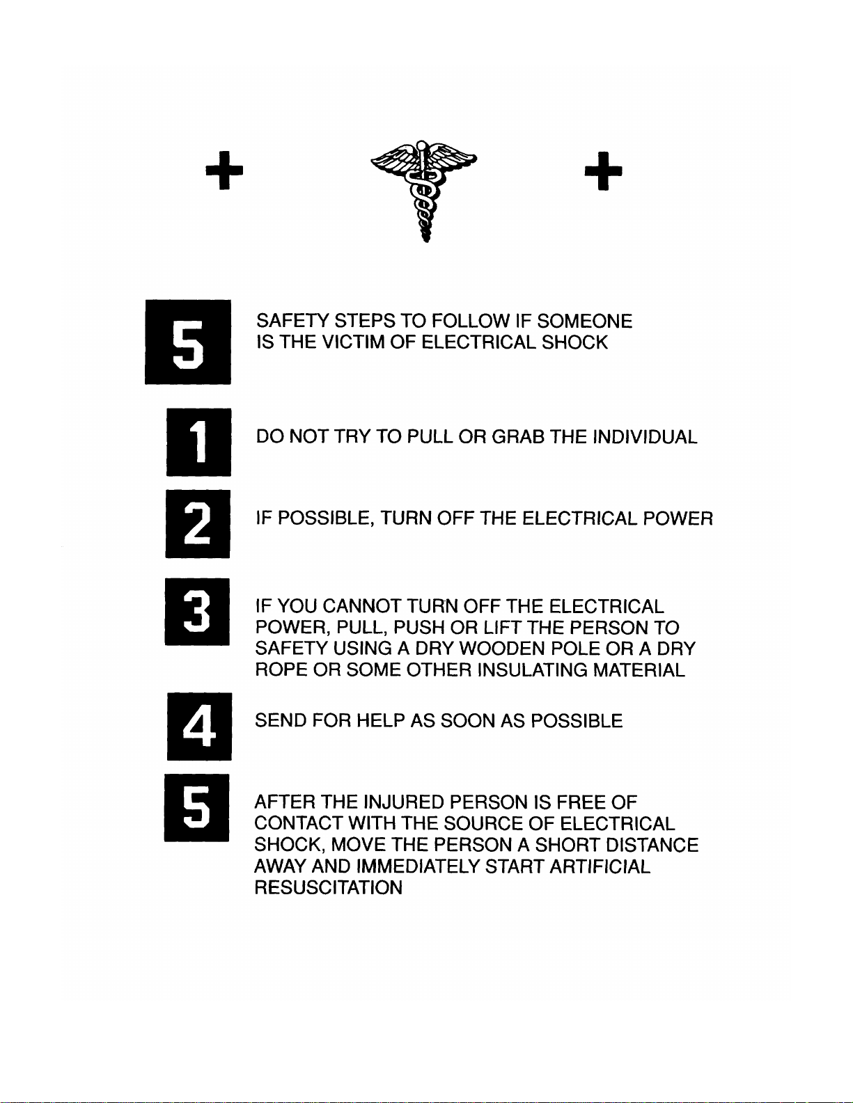
SAFETY
TM 11-6625-2837-14&P-7
WARNING
Although this instrument has been designed in
accordance with international safety standards, this
manual contains information, cautions, and warnings
which must be followed to retain the instrument in safe
condition. Be sure to read and follow the safety
information in Sections 11, III, V, an VIII.
BEFORE CONNECTING THIS SYSTEM TO LINE
(MAINS) VOLTAGE, the safety and installation
instructions found in Sections II and III of the m ainfram e
manual should be followed.
HIGH VOLTAGE
Adjustments and troubleshooting are often performed
with power supplied to the instrument while protective
covers are removed. Energy available at many points
may constitute a shock hazard
The multi-pin plug connector which provides inter
connection from mainframe to RF Section, will be
exposed with the RF Section removed from the righthand mainframe cavity. With the Line (Mains Voltage off
and power cord disconnected, power supply voltages
may still remain and may constitute a shock hazard.
COMPATIBILITY
Damage to the synthesized signal generator system m ay
result if an option 002 RF Section is used with
unmodified Model 8660A or 8660B main-frames with
serial prefixes 1349A and below.
PERFORMANCE TESTING
To avoid the possibility of damage to the instrum ent or
test equipment, read completely through each test before
starting it. Then make any preliminary control settings
necessary before continuing with the procedure.
PLUG-IN REMOVAL
Before removing the RF Section plug-in from the
mainframe, remove the line (Mains) voltage by
disconnecting the power cable from the power outlet.
SEMI-RIGID COAX
Slight but repeated bending of the semi-rigid coaxial
cable will damage them very quickly. Bend the cables as
little as possible. If necessary, loosen the assembly to
release the cable.
WARNING
Voltages are present in this instrument, when energized, which can
cause death on contact.
The multi-pin plug connector which provides interconnection from
mainfram e to RF Section, will be exposed with the RF Sect ion removed
from the righthand mainfram e cavity. With the line voltage of f and power
cord disconnected, power supply voltage may still remain and may
constitute a shock hazard.
A
Page 4

TM 11-6625-2837-14&P-7
This manual contains copyrighted material reproduced by permission of the Hewlett-Packard Company. All rights
reserved.
TM 11-6625-2825-14&p-7
TECHNICAL MANUAL ) HEADQUARTERS
) DEPARTMENT OF THE ARMY
No. 11-6625-2825-14&p-7 ) Washington, D.C., 18 October 1981
OPERATOR’S, ORGANIZATIONAL, DIRECT SUPPORT
AND GENERAL SUPPORT MAINTENANCE MANUAL
INCLUDING REPAIR PARTS AND SPECIAL TOOLS LISTS
FOR
RF SECTION PLUG-IN, HEWLETT-PACKARD MODEL 86602B
(NSN 6625-01-031-8853)
CURRENT AS OF 30 JANUARY 1981
REPORTING ERRORS AND RECOMMENDING IMPROVEMENTS
You can help improve this manual. If you find any mistakes or if you know of a way to improve the procedures,
please let us know. Mail your letter or DA Form 2028 (R ecommended Changes to Publications and Blank Forms), direc t
to: Commander, US Army Communications and Electronics Materiel Readiness Command, ATTN: DRSEL-ME-MQ, Fort
Monmouth, New Jersey 07703. In either case, a reply will be furnished direct to you.
This manual is an authentication of the manufacturer’s commercial literature which, through usage, has been found to
cover the data required to operate and maintain this equipment. The manual was not prepared in acc or dance with military
specifications; therefore, the format has not been st ructured to consider categories of maintenance. Section IX contains
improvements made after the printing of the manufacturer’s manual.
CONTENTS
SECTION 0 INTRODUCTION PAGE
0-1. Scope 0-1
0-2. Indexes of Publications 0-1
0-3. Maintenance Forms, Records and Reports 0-1
0-4. Reporting Equipment Improvement Recommendations (EIR) 0-1
0-5. Administrative Storage 0-2
0-6. Destruction of Army Electronics Materiel 0-2
i
Page 5

CONTENTS
TM 11-6625-2837-14&P-7
Section Page
I GENERAL INFORMATION......................... 1-1
1-1. Introduction....................................... 1-1
1-7. Specifications .................................. 1-1
1-9. Instruments Covered by Manual....... 1-1
1-12. Manual Change Supplements.......... 1-1
1-15. Description........................................ 1-5
1-20. Options ............................................ 1-5
1-24. Compatibility..................................... 1-5
1-27.Equipment Required but not
Supplied........................................ 1-5
1-28.System Mainframe........................... 1-5
1-31.Frequency Extension Module........... 1-6
1-33.Auxiliary Section............................... 1-6
1-35.Modulation Section Plug-ins............. 1-6
1-37.Equipment Available......................... 1-6
1-40.Safety Considerations...................... 1-6
1-43.Recommended Test Equipment....... 1-6
II INSTALLATION........................................... 2-1
2-1. Introduction....................................... 2-1
2-3. Initial Inspection ............................... 2-1
2-5. Preparation For Use......................... 2-1
2-6. Power Requirements........................ 2-1
2-8. Interconnections............................... 2-1
2-10.Modifications..................................... 2-1
2-13.Operating Environment..................... 2-1
2-15.Installation Instructions..................... 2-1
2-17.Storage and Shipment...................... 2-2
2-18.Environment..................................... 2-2
2-20.Packaging......................................... 2-2
III OPERATION........................................... 3-1
3-1. Introduction ...................................... 3-1
3-3. Panel Features................................. 3-1
3-5. Operator’s Check.............................. 3-1
3-8. Operating Instructions ..................... 3-1
IV PERFORMANCE TESTS ....................... 4-1
4-1. Introduction....................................... 4-1
4-3. Equipment Required......................... 4-1
4-5. Test Record...................................... 4-1
4-7. Performance Tests........................... 4-1
4-9. Frequency Range............................. 4-2
4-10.Frequency Accuracy and Stability.... 4-3
4-11.Frequency Switching Time............... 4-3
4-12.Output Level Switching Time............. 4-5
4-13A. Output Accuracy.......................... 4-7
4-13B. Output Accuracy- Alternate
Procedure...................................... 4-12
4-14.Output Flatness................................ 4-15
4-15.Harmonic Signals............................. 4-16
Section Page
4-16.Pulse Modulation Risetime............... 4-17
4-17.Pulse Modulation On/Off Ratio......... 4-19
4-18.Amplitude Modulation Depth and
3 dB Bandwidth............................. 4-19
4-19.Frequency Modulation Rate and
Deviation....................................... 4-23
4-20.Output Impedance and VSWR......... 4-23
4-21.Signal-to-Phase Noise Ratio............ 4-25
4-22.Signal-to-AM Noise Ratio................. 4-27
4-23.Residual FM..................................... 4-29
4-24.Amplitude Modulation Distortion...... 4-31
4-25.Incidental Phase Modulation ........... 4-33
4-26.Frequency Modulation Distortion...... 4-35
4-27.Incidental AM................................... 4-38
4-28.Spurious Signals, Narrowband......... 4-40
4-29.Spurious Signals, Wideband............ 4-41
4-30.Phase Modulation Peak Deviation... 4-43
4-31A. Phase Modulation Distortion........... 4-43
4-31B. Phase Modulation Distortion -
Alternate Procedure...................... 4-45
V ADJUSTMENTS.......................................... 5-1
5-1. Introduction...................................... 5-1
5-4. Equipment Required........................ 5-1
5-8. Safety Considerations...................... 5-1
5-12.Factory Selected Components......... 5-1
5-14.Related Adjustments........................ 5-1
5-18.Adjustment Locations....................... 5-2
5-20.Adjustments..................................... 5-2
5-22.Post Adjustment Tests .................... 5-2
5-24.RF Output Level Adjustment............ 5-3
5-25.1 dB Step Attenuator Adjustment..... 5-4
5-26.Amplitude Modulation Input Circuit
Adjustment.................................... 5-5
5-27.Phase Modulator Driver Frequency
Response Adjustments................. 5-7
5-28A. Phase Modulation Level and
Distortion Adjustments.................. 5-8
5-28B. Phase Modulation Level and Distortion
Adjustments - Alternate Procedure5-11
VI REPLACEABLE PARTS.......................... 6-1
6-1. Introduction...................................... 6-1
6-3. Exchange Assemblies...................... 6-1
6-5. Abbreviations................................... 6-1
6-7. Replaceable Parts List..................... 6-1
ii
Page 6

CONTENTS (Cont’d)
TM 11-6625-2837-14&P-7
Section Page
VII MANUAL CHANGES ............................... 7-1
7-1. Introduction ...................................... 7-1
7-3. Manual Changes.............................. 7-1
7-6. Manual Change Instructions............. 7-2
VIII SERVICE................................................... 8-1
8-1. Introduction....................................... 8-1
8-8. Safety Considerations...................... 8-1
8-12.Principles of Operation..................... 8-1
8-16.Troubleshooting................................ 8-1
ILLUSTRATIONS
Figure Page
1-1. HP Model 86602B RF Section (Opt. 002
Shown)
1-2. 40 dB Test Amplifier................................ 1-0
1-3. 15 kHz Low Pass Filter .......................... 1-11
1-4. Low Pass Filters...................................... 1-11
2-1. RF Section Partially Inserted into
Mainframe........................................ 2-2
3-1. Front Panel Controls, Connectors, and
Indicators.......................................... 3-2
3-2. Rear Panel Connectors and Indicators... 3-3
3-3. Operator’s Check.................................... 3-4
4-1. Frequency Range Test Setup................. 4-2
4-2. Frequency Switching Time Test Setup... 4-4
4-3. Output Level Switching Time Test Setup 4-6
4-4A.Output Accuracy Test Setup.................. 4-8
4-4B.Output Accuracy Test Setup (Alternate
Procedure......................................... 4-13
4-5. Pulse Modulation Risetime Test Setup .. 4-18
4-6. Amplitude Modulation, Depth and 3 dB
Bandwidth Test Setup...................... 4-20
4-7. Output Impedance Test Setup................ 4-24
4-8. Signal-to-Phase Noise Ratio Test Setup. 4-26
4-9. Signal-to-AM Noise Ratio Test Setup..... 4-28
4-10.Residual FM Test Setup......................... 4-29
4-11.Amplitude Modulation Distortion Test
Setup................................................ 4-30
4-12.Incidental Phase Modulation Test Setup 4-32
4-13.Frequency Modulation Distortion Test
Setup................................................ 4-35
4-14.Incidental AM Test Setup ....................... 4-38
4-15.Narrowband Spurious Signal Test Setup. 4-39
4-16.Wideband Spurious Signal Test Setup... 4-41
Section Page
8-17.System Troubleshooting.................. 8-2
8-19.RF Section Troubleshooting............. 8-2
8-21.Troubleshooting Aids....................... 8-2
8-28.Recommended Test Equipment...... 8-2
8-30.Repair............................................... 8-2
8-31.General Disassembly Procedures.... 8-2
8-34.Non-Repairable Assemblies............. 8-2
8-36.Module Exchange Program.............. 8-3
8-38.Repair Procedures........................... 8-3
8-42.Post Repair Adjustments................. 8-3
IX ERRATA
Figure Page
4-17A. Phase Modulation Distortion Test Setup 4-44
4-17B.Phase Modulation Distortion Test Setup
(Alternate Procedure)....................... 4-46
5-1. RF Output Level Adjustment Test Setup 5-3
5-2. 1 dB Step Attenuator Adjustment Test
Setup................................................ 5-4
5-3. Amplitude Modulation Input Circuit
Adjustment Test Setup..................... 5-5
5-4. Phase Modulator Driver Frequency
Response Adjustment Test Setup... 5-7
5-5A.Phase Modulation Level and Distortion
Adjustment Test Setup..................... 5-9
5-5B.Phase Modulation Level and Distortion
Adjustment Test Setup (Alternate
Procedure)....................................... 5-12
7-1. Phase Modulator Driver Frequency Response
Adjustment Test Setup (Change B). 7-2
7-2. A16 Phase Modulator Driver Assembly
Component and Test Point Locations
(Change B)....................................... 7-6
7-3. Phase Modulation Section Schematic
Diagram (Option 002) (Change B)... 7-8
7-4. A17 Phase Modulator Assembly
Component Locations (Change C).. 7-9
7-5. P/O Phase Modulation Section Schematic
Diagram (Change C)........................ 7-11
7-6. P/O Attenuator Section Schematic
Diagram (Change D)........................ 7-11
7-7. P/O All Logic Assembly Schematic
Diagram (Change E)........................ 7-12
8-1. LO Signal Circuits Repair....................... 8-4
iii
Page 7

ILLUSTRATIONS (Cont’d)
TM 11-6625-2837-14&P-7
Figure Page
8-2. Rear Panel Disassembly......................... 8-8
8-3. Schematic Diagram Notes...................... 8-9
8-4. System Test Point Locations.................. 8-17
8-5. Mainframe Interconnect Jack.................. 8-17
8-6. System Troubleshooting Block
Diagram............................................ 8-17
8-7. RF Section Simplified Block Diagram..... 8-19
8-8. Main Troubleshooting Block Diagram .... 8-19
8-9. Logic Troubleshooting Block Diagram ... 8-21
8-10.A7 Mixer Assembly’s Subassembly and
Component Location........................ 8-22
8-11.Mixer Section Schematic Diagram.......... 8-23
8-12.A16 Phase Modulator Driver Assembly
Component and Test Point Locations 8-25
8-13.A17 Phase Modulator Assembly
Component Locations ..................... 8-25
8-14.Phase Modulation Section Schematic
Diagram (Option 002)....................... 8-25
8-15.A4 Detector Amplifier Assembly
Component and Test Point Locations 8-27
Figure Page
8-16..Amplifier/Detector Section
Schematic Diagram.......................... 8-27
8-17.A3 ALC Amplifier Assembly Component
and Test Point Locations.................. 8-28
8-18.A10 Reference Assembly
Component Locations ..................... 8-29
8-19.A2 ALC Mother Board Assembly
Component Locations...................... 8-29
8-20.ALC Section
Schematic Diagram.......................... 8-29
8-21.A9 Attenuator Driver Assembly
Component Locations ..................... 8-31
8-22.Attenuator Section
Schematic Diagram.......................... 8-31
8-23.All Logic Assembly
Component Locations...................... 8-33
8-24.All Logic Assembly
Schematic Diagram.......................... 8-33
8-25.Assemblies, Chassis Parts, and Adjustable
Component Locations ..................... 8-35
TABLES
Table Page
1-1. Models 86602B/11661 Specifications..... 1-2
1-2. Recommended Test Equipment............. 1-7
3-1. Operating Instructions ............................ 3-6
4-1. dB to Power Ratio Conversion................ 4-37
4-2. Narrowband Spurious Signal Checks..... 4-40
4-3. Wideband Spurious Signal Checks........ 4-41
4-4. Performance Test Record ...................... 4-47
5-1. Factory Selected Components................ 5-2
APPENDIX A. References............................................................................................. A-1
APPENDIX B. Maintenance Allocation
Section I. Introduction............................................................................................. B-1
II. Maintenance Allocation.......................................................................... B-5
III. Tool and Test Equipment Requirements............................................ B-6
Users of this manual are advised to consult SECTION IX, ERRATA. SECTION IX
contains errors and changes in text and illus trations. The user should correc t the errors
and perform the changes indicated, as needed.
Table Page
6-1. Reference Designations & Abbreviations6-3
6-2. Replaceable Parts.................................. 6-5
6-3. Code Lists of Manufacturers................... 6-15
6-4. Parts to NSN Cross Refererence........... 6-16
7-1. Manual Changes by Serial Prefix........... 7-1
7-2. Summary of Changes by Component.... 7-1
7-3. Replaceable Parts (P/O Change B)........ 7-7
8-1. Front Panel Housing Repair................... 8-7
8-2. Adjustable Components Locations.. 8-34
APPENDICES
Page
NOTE
iv
Page 8

TM 11-6625-2837-14&P-7
SECTION 0
INTRODUCTION
0-1. Scope
This manual describes RF Section Hewlett-Packard Model 86602B, hereinafter referred to as the RF Section, and
provides instructions for its operation and maintenance.
This manual applies dir ectly to instruments with serial numbers prefixed 1638A. It is also applicable to instruments with
other serial number prefixes for which manual changes are given in SECTION VII.
SECTION VI includes Table 6-4, a cross reference between the Hewlett-Packard part numbers and the equivalent
NATO/NATIONAL Stock Numbers (NSN).
Appendix A provides a reference of pertinent Department of the Army publications.
Appendix B contains the Maintenance Allocation Chart (MAC) which defines the levels and scope of maintenance
functions for the equipment in the Army system and a list of the tools and test equipment required.
0-2. Indexes of Publications
a. DA Pam 310-4
changes or additional publications pertaining to the equipment.
b. DA Pam 310-7
pertaining to the equipment.
0-3. Maintenance Forms, Records and Reports
a. Reports of Maintenance and Unsatisfac tory Equipment. Departm ent of the Arm y form s and procedures
used for equipment maintenance will be those prescribed by TM 38-750, the Army Maintenance Management System.
b. Report of Item and Packaging Discr epancies. Fill out and forward SF 364 ( Report of Discr epancy (ROD) as
prescribed in AR 735-11-2/DLAR 4140.55/NAVSUPINST 4440.127E/AFR 400.54/MCO 4430.E.
c. Discrepancy in Shipment Report (DISREP) (SF 361). Fill out and forward Disc repancy in Shipment Report
(DISREP) (SF 361) as prescribed in AR 55-38/NAVSUPINST 4610.33B/AFR 75-18/MCO P4610.19C and DLAR 4500.15.
0-4. Reporting Equipment Improvement Recommendations (EIR)
If your HP 86602B RF Section needs improvement, let us know. Send us an EIR. You, the user, are the only one
who can tell us what you don’t like about your equipment. Let us know why you don’t like the design. Tell us why a
procedure is hard to perform. Put it on an SF 368 (Quality Deficiency Report). Mail it to: Commander, US Army
Communications - Electronics Comm and, AT TN : DRSEL-ME-MQ, Fort Monm outh, New Jers ey 07703. W e’ll send you a
reply.
. Refer to the latest issue of the DA Pam 310-4 to determine whether there are new editions,
. Refer to DA Pam 310-7 to determine whether there are Modification Work Orders (MWOs)
0-1
Page 9

0-5. Administrative Storage.
Store in accordance with Paragraphs 2-17 through 2-22.
0-6. Destruction of Army Electronics Materiel
Destruction of Army electronics materiel to prevent enemy use shall be in accordance with TM 750-244-2.
TM 11-6625-2837-14&P-7
0-2
Page 10
Section 1 TM 11-6625-2837-14&P-7
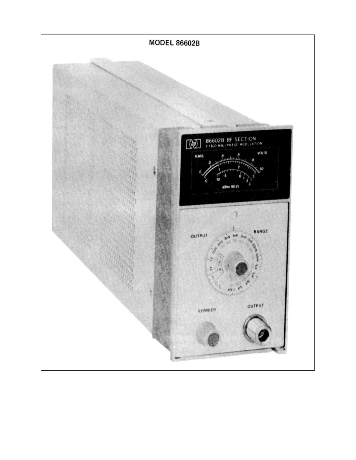
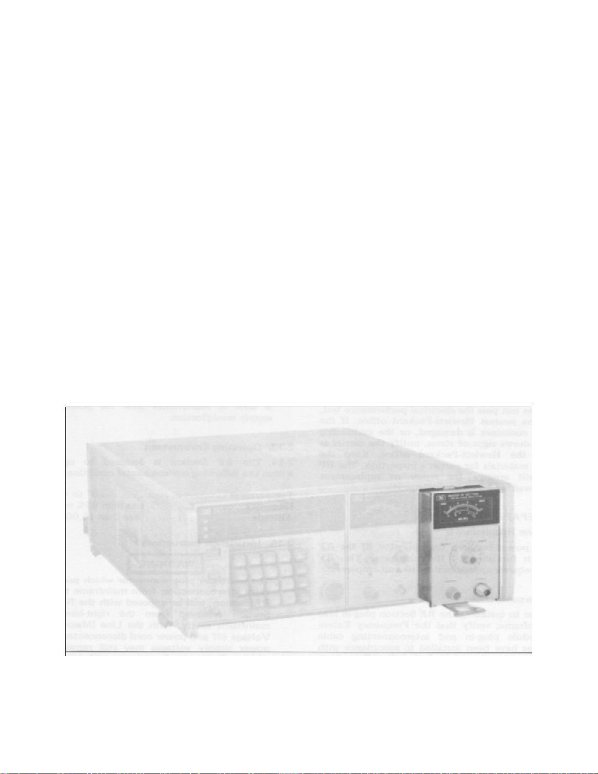
Figure 1-1. HP Model 86602B RF Section (Option 002 Shown)
1-0
Page 11

Section 1 TM 11-6625-2837-14&P-7
SECTION I
GENERAL INFORMATION
1-1. INTRODUCTION
1-4. Figure 1-1 shows the Option 002 RF Section.
1-2. This manual contains all information required to
install, operate, test, adjust and service the HewlettPackard Model 86602B RF Section plug-in, hereinafter
referred to as the RF Section. For information
concerning related equipment, such as the HewlettPackard Model 8660-series mainframes or the Model
11661 Frequency Extension Module, refer to the
appropriate manual or manuals.
1-3. This manual is divided into eight sections which
provide information as follows:
a. SECTION I, GENERAL INFORMATION,
contains the instrument desc ription and specific ations as
well as the accessory and recomm ended test equipment
list.
b. SECTION II, INSTALLATION, contains
information relative to receiving inspection, preparation
for use, mounting, packing, and shipping.
c. SECTION III, OPERATION, contains
operating instructions for the instrument.
d. SECTION IV, PERFORMANCE TESTS,
contains information required to verify that instrument
performance is in accordance with published
specifications.
e. SECTION V, ADJUSTMENTS, contains
information required to properly adjust and align the
instrument after repair.
f. SECTION VI, REPLACEABLE PARTS,
contains information required to order all replacement
parts and assemblies.
g. SECTION VII, MANUAL CHANGES, provides
information to docum ent all serial number prefixes listed
on the title page.
h. SECTION VIII, SERVICE, contains
descriptions of the circuits, schematic diagrams, parts
location diagrams, and troubleshooting pr ocedures to aid
the user in maintaining the instrument.
1-5. DELETED
1-6. On the title page of this manual, below the manual
part number, is a “Microf ic he” par t number. This number
may be used to order 4 x 6-inch microfilm transparencies
of the manual. Each m icrof iche contains up to 60 photoduplicates of the manual pages. The microfiche
package also includes the latest Manual Changes
supplement as well as all pertinent Service Notes.
1-7. SPECIFICATIONS
1-8. Instrument spec ifications are listed in T able 1-1.
These specifications are the per formance standards, or
limits against which the instrument may be tested.
1-9. INSTRUMENTS COVERED BY MANUAL 1-10.
This instrument has a two-part serial number. The f irst
four digits and the letter comprise the serial number
prefix. The last f ive digits form the sequential suff ix that
is unique to each instrument. The contents of this
manual apply directly to instruments having the same
serial number prefix(es) as listed under SERIAL
NUMBERS on the title page.
1-11. For information concerning a serial num ber prefix
not listed on the title page or in the Manual Changes
supplement, contact your nearest Hewlett-Packard
office.
1-12. MANUAL CHANGE SUPPLEMENTS
1-13. An instrument manufactured after the printing of
this manual may have a serial prefix that is not lis ted on
the title page. This unlisted serial
1-1
Page 12
Section 1 TM 11-6625-2837-14&P-7
Table 1-1. Models 86602B/11661 Specifications (1 of 3)
SPECIFICATIONS
FREQUENCY CHARACTERISTICS
Spurious Signals (CW, AM, and OM only):
Range: 1.0 to 1299.999999 MHz selectable in 1 Hz
steps. Frequencies from 200 k Hz to 1 MHz may also be
selected with some degradation in specifications.
1
Accuracy and Stability
: CW f requency accuracy and
long term stability are determined by the aging rate of the
80 dB down from carrier at frequencies <700 MHz
80 dB down from carrier within 45 MHz of the carrier at
frequencies >700 MHz
70 dB down from carrier >45 MHz from carrier at
frequencies >700 MHz
50 dB down from carrier on the +10 dBm range.
time base (internal or external) and its sensitivity to
changes in temperature and line voltage. Internal
reference oscillator ac curacy = + aging rate ± 3 x 10
/°C + 3 x 10
-10
/1% change in line voltage
-10
All Power Line Related spurious signals are 70 dB down
from carrier.
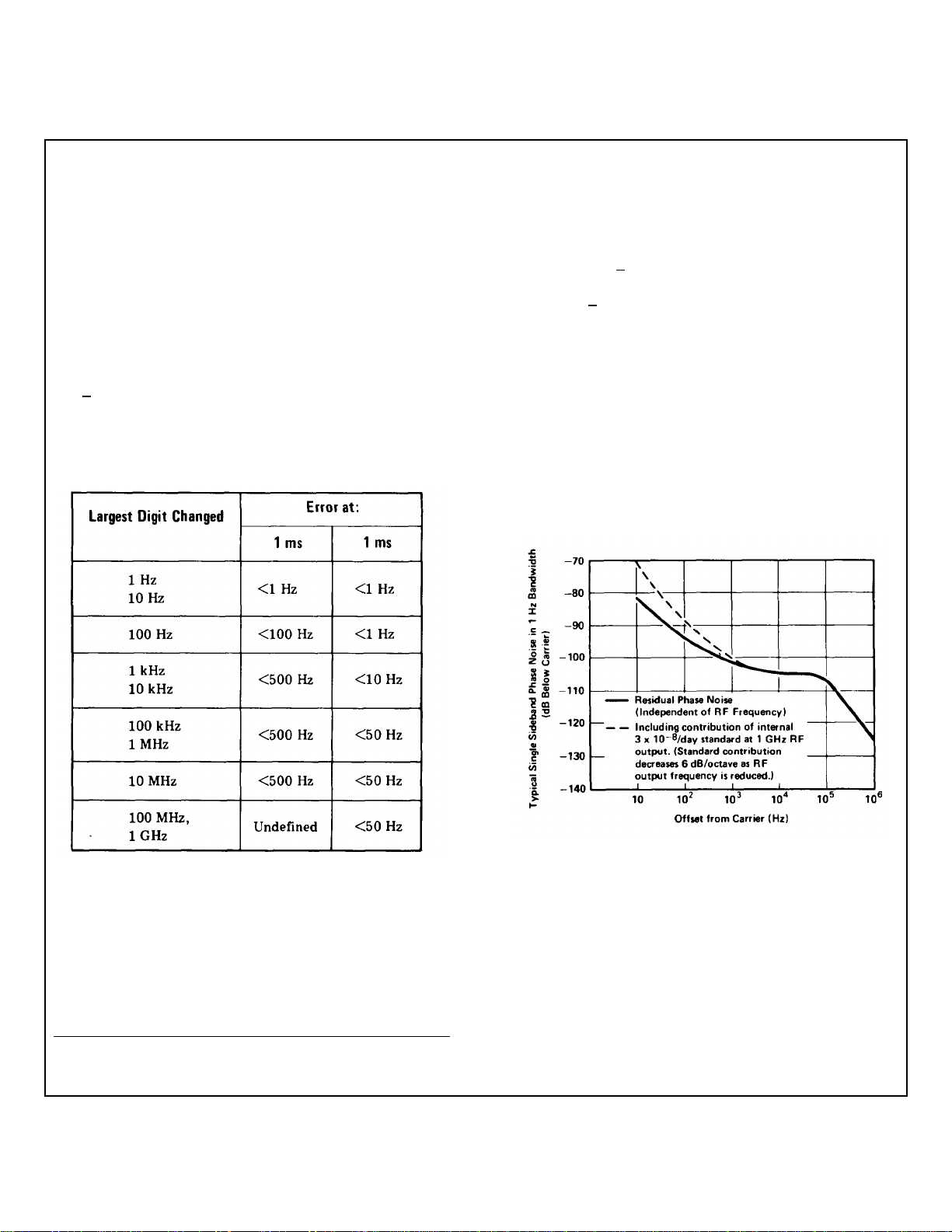
Switching Time: 6 ms to be within 50 Hz of any new
frequency selected; 100 ms to be within 5 Hz of any new
frequency delected.
Typical 86602B/11661 Frequency Switching
Characteristics
Harmonic Signals:
All harmonically related signals are at least 30 dB below
the desired output signal for output levels <+3 dBm.
(25 dB down for output levels above +3 dBm.)
Signal-to-Phase Noise Ratio (CW, AM, and OM only):
Greater than 45 dB in a 30 kHz band centered
on the carrier and excluding a 1 Hz band
centered on the carrier.
Typical SSB Phase Noise Curve:
Typical 86602B Phase Noise
Signal-to-AM Noise Ratio: Greater than 65 dB down in
a 30 kHz bandwidth centered on the carrier and
excluding a 1 Hz band centered on the carrier
1
Aging rate for the time base of standard mainframes is 3 x
10-8/day: for option 001 mainframes, 3 x 10⁻⁹/day.
1-2
Page 13
Section 1 TM 11-6625-2837-14&P-7
Table 1-1. Models 86602B/11661 Specifications (2 of 3)
OUTPUT CHARACTERISTICS
Level: Continuously adjustable from +10 to -146 dBm
(0.7 Vrms to 0.01 /Vrms) into a 50Q resistive
load. Output attenuator calibrated in 10 dB steps
from 1.OV full scale (+10 dBm range) to 0.03
pVrms full scale (-140 dBm range). Vernier
provides continuous adjustment between
attenuator ranges. Output level indicated on
output level meter calibrated in volts and dBm
into 50 ohms.
Accuracy: (Local and remote modes)
+ 1.5 dB to -76 dBm; + 2.0 dB to -146 dBm at
meter readings between +3 and -6 dB.
Flatness: Output level variation with frequency is less
than ±1.0 dB from 1-1300 MHz at meter
readings between +3 and --6 dB.
Level Switching Time: In the remote mode any level
change can be accomplished in les s than 50 ms.
Any change to another level on the same
attenuator range can be accomplished in less
than 5 ms.
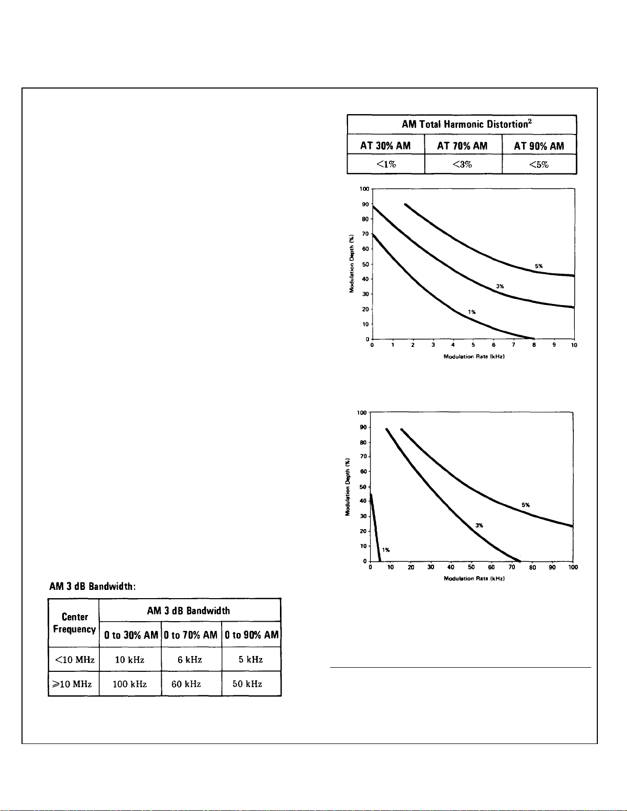
Typical AM Distortion (Center Frequency <10 MHz)
Impedance: 50Q.
VSWR: <2.0 on +10 and O dBm range; <1.3 on -10 dBm
range and below.
MODULATION CHARACTERISTICS
(With compatible Modulation Sections)
Amplitude Modulation:
Depth: 0 - 90% for RF output level meter readings from
+3 to -6 dB and only at +3 dBm and below.
AM 3 db Bandwidth:
Typical AM Distortion (Center Frequency > 10 MHz)
Incidental PM: Less than 0.2 radians peak at 30% AM.
Incidental FM: Less than 0.2 times the frequency of
modulation (Hz) at 30% AM.
2
Applies only at 400 Hz and 1 kHz rates with the RF Section
front panel meter indicating from O to +3 dBm. At a meter
indication of 6 dB the distortion approximately doubles. The
modulating signal distortion must be <0.3% for the system
performance to meet these specifications.
1-3
Page 14
Section 1 TM 11-6625-2837-14&P-7
Table 1-1. Models 86602B/1 1661 Specifications (3 of 3)
FREQUENCY MODULATION
Rate: DC to 200 kHz with the 86632B and 86635A.
20 Hz to 100 kHz with the 86633B.
Maximum Deviation (peak):
200 kHz with the 86632B and 86635A
100 kHz with the 86633B
Incidental AM: AM sidebands are greater than 60 dB
down from the carrier with 75 kHz peak deviation
at a 1 kHz rate.
FM Total Harmonic Distortion (at rates up to 20 kHz);
<1% up to 200 kHz deviation. (External
modulating signal distortion must be less than
0.3%.)
Residual FM: less than 10 Hz rms average in 300 kHz,
Post-detection bandwidth, FM x 0.1 mode.
ON/OFF Ratio: At least 40 dB.
Input Level Required: -10-+ 0.5 Vdc turns RF on.
PHASE MODULATION
(Option 002 Instruments only)
Rate:
with 86635A dc to 1 MHz
with 86634A
dc to 1 MHz at center frequencies less than 100
MHz dc to 10 MHz at center frequencies greater
or equal to 100 MHz.
Maximum Peak Deviation:
0 to 100 degrees peak. May be overdriven to 2 radians
(1150) in the Modulation Section’s external dc
mode.
∅M Distortion:
<5% up to 1 MHz rates
<7% up to 5 MHz rates
<15% up to 10 MHz rates
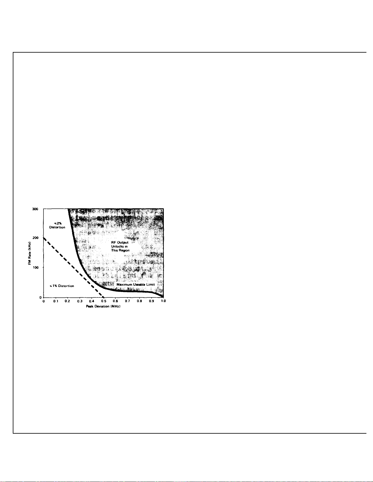
Typical FM Distortion Curve
PULSE MODULATION
(With the 86631B Auxiliary Section only)
Source: External
Rise/Fall Time: 50 ns.
(External modulation signal distortion m ust be less than
0.3% to meet this specification.)
REMOTE PROGRAMMING
(Through the 8660-series mainframes)
Frequency: Programmable in 1 Hz steps.
Output Level: Programmable in 1 dB s teps from +10 to
-146 dBm.
Modulation: See specifications for modulation section
installed.
GENERAL
Leakage: Meets radiated and conducted limits of MIL-I-
6181D.
Size: Plug-in to fit 8660-series mainframe.
Weight: Net 9 lb (3.9 kg).
1-4
Page 15

Section 1 TM 11-6625-2837-14&P-7
prefix indicates that the instrument is different fr om those
documented in this manual. The manual for this
instrument is supplied with a yellow Manual Changes
supplement that contains “change information” that
documents the differences.
1-14. In addition to change information, the supplem ent
may contain information for correcting errors in the
manual. To keep this manual as current and accurate as
possible, Hewlett-Packard recommends that you
periodically request the latest Manual Changes
supplement. The supplem ent for this m anual is k eyed to
this manual’s print date and part number , both of which
appear on the title page. Complimentary copies of the
supplement are available from Hewlett-Packard.
1-15. DESCRIPTION
1-16. The HP Model 86602B RF Section is one of
several RF Sections available for us e in an 8660-series
Synthesized Signal Generator System. This RF Sec tion
plug-in is used with an option 100 8660-series
mainfram e (Frequenc y Extension Module installed). T he
RF Section provides precisely tuned RF output
frequencies over the 1 to 1300 MHz range with 1 Hz
frequency resolution (8660-series option 004 instr uments
have resolutions of 100 Hz.) Frequencies from 200 k Hz
to 1 MHz can also be generated with some degradation
in the amplitude leveling and other related specifications.
1-17. The output power can be set to any level between
+10 and --146 dBm by means of the front panel
VERNIER and calibrated OUTPUT RANGE controls. A
front panel-mounted meter and the OUTPUT RANGE
switch indicate the output power and voltage levels
delivered by the RF Section to any external load having a
characteristic impedance of 50 ohms. Output power
levels are maintained within + 1 dB of selected values
through internal leveling of the output signal over the full
frequency range of the instrument.
1-18. Amplitude, frequency, phase, or pulse modulation
of the RF OUTPUT signal can be accomplished within
the RF Section by using the appropriate Auxiliary or
Modulation Section plug-in.
1-19. External programm ing perm its rem ote selection of
the output signal frequency in 1 Hz steps (100 Hz for
option 004 mainframes) and the output power in 1 dB
steps over the full operating
range of the instrument. External programming is
accomplished via the mainframe computer-compatible
interface and digital control unit circuits.
1-20. OPTIONS
1-21. This RF Section has two options available. They
affect the instrument’s RF output level, and phase
modulation capabilities.
1-22. Option 001. The RF output attenuator is
removed. This lim its the RF output level range f rom +10
to -6 dBm.
1-23. Option 002. Circuits are added to provide the
phase modulation capability. A compatible modulation
section is required.
1-24. COMPATIBILITY
1-25. Except for Option 002 instruments, the Model
86602B is compatible with all 8660-series option 100
mainframes, all AM-FM Modulation Sections and the
Auxiliary Section. This RF Section is partially com patible
with the FM/OM Modulation Section.
Damage to the signal generator system
may result if an option 002 RF Section
is used with Model 8660A or 8660B
main-frames with serial prefixes 1349A
and below.
1-26. Option 002 instruments are compatible with all
instruments which are part of the Model 8660-series
Synthesized Signal Generator System except early
model 8660A and 8660B Mainframes. Refer to the
paragraph entitled Modifications in Section II of this
manual for further information.
1-27. EQUIPMENT REQUIRED BUT NOT
SUPPLIED
1-28. System Mainframe
1-29. The mainframe uses phase-locked loops to
accurately generate clock, referenc e, and tuning signals
required for operation of the Synthesized Signal
Generator System. Front panel-mounted mainframe
controls are used to digitally tune two phase-locked loops
in the Frequency Extension Module which, in turn,
produce two high-frequency output signals that are
applied to the RF Section. The RF Section mixes the
two signals
1-5
Page 16

Section 1 TM 11-6625-2837-14&P-7
and presents their frequency difference at the front panel
OUTPUT jack. The output frequency is either the value
selected by the mainframe front panel controls or
external programming.
1-30. The mainframe power supply provides all dc
operating voltages required by the RF Section,
Frequency Extension Module, and Modulation Section
plug-ins. Remote programming of the plug-ins is
accomplished via the mainframe interface and digital
control unit circuits.
1-31. Frequency Extension Module
1-32. The Frequency Extension Module plug-in extends
the output frequency range of the main-frame to meet
the input requirements of the RF Section. The
Frequency Extension Module plug-in contains two highfrequency phase-locked loops which receive digital
tuning signals, variable synthesized signals, and fixed
synthesized signals from the mainframe. The phaselocked loops use the main-frame signals, in conjunc tion
with the output frequency from a 4.43 GHz oscillator that
is common to both loops, to produce two high-frequency
output signals that are supplied to the RF Section. O ne
output signal is generated by a phase-locked loop using
a Voltage Controlled Oscillator (VCO) that is tuneable in
1 Hz steps (100 Hz steps for option 004 mainframe) over
the 3.95 to 4.05 GHz range. The other output signal is
generated by a phase-locked loop using a Yittrium-IronGarnet (YIG) oscillator that is tunable in 100 MHz steps
over the 3.95 to 2.75 GHz range. The two outputs from
the Frequency Extension Module plug-in are applied to
the RF Section for mixing, amplification of the converted
signal, and final output power level control.
1-33. Auxiliary Section
1-34. The Auxiliary Section plug-in provides a means of
applying externally generated amplitude or pulse
modulation drive signals to modulate the RF Section’s
output carrier.
1-35. Modulation Section Plug-ins
1-36. The Model 86630-series Modulation Section plugins can accept external modulation drive signals or
generate internal drive signals to amplitude, frequency,
phase or pulse modulate the RF Sections output signal.
1-37. EQUIPMENT AVAILABLE
1-38. Extender cables, coaxial adapters, and an
adjustment tool are available for use in performance
testing, adjusting, and maintaining the RF Section. Each
piece may be ordered separately or as part of the
11672A Service Kit.
1-39. Extender cards for use in ser vicing the RF Section
and a type N to BNC adapter for use on the front panel
RF OUTPUT connector are contained in the HP Rack
Mount Kit, Part Number 08660-60070, that is supplied
with the mainframe.
1-40. SAFETY CONSIDERATIONS
1-41. This instrument has been designed in accord-ance
with international safety standards and has been
supplied in safe condition.
1-42. Although this instrument has been designed in
accordance with international safety standards, this
manual contains information, cautions, and warnings
which must be followed to retain the instrument in sa fe
condition. Be sure to read and follow the safety
information in Sections II, III, V, and VIII.
1-43. RECOMMENDED TEST EQUIPMENT 1-44.
Table 1-2 lists the test equipment and accessories
recommended for use in testing, adjusting, and s ervicing
the RF Section. If any of the recommended test
equipment is unavailable, instruments with equivalent
specifications may be used. See Appendix B, Section III.
1-6
Page 17

Section 1 TM 11-6625-2837-14&P-7
See Appendix B, Section III
Table 1-2. Recommended Test Equipment (1 of 4)
Item Critical Specifications Suggested Model Use*
Adapter (Male Type N Frequency range 100 MHz to 1.3 GHz HP 1250-0847 P
to GR874 )
Adapter, SMA-to-BNC 2 required OSM 21190 P
Adapter, SMA-to-OSM OSM 219 P
Right Angle
Adapter, Type N-to- OSM 21040 P
SMA
Amplifier, 20 dB -20 dB gain at 30 MHz HP 8447A P
Input SWR <1.7
Amplifier, 40 dB Special (see Figure 1-2) P
Analyzer, Distortion 20 Hz to 20 kHz; must measure <0.1% distortion HP 333A P
Analyzer, Spectrum Measurement Accuracy +2.0 dB from 1 kHz HP 8553B with HP 8552B P.,A
to 110 MHz and HP 1-10T
Analyzer, Spectrum Measurement Accuracy +2.0 dB from 10 MHz HP 8555A with HP 8552B P. A, T
to 8 GHz and HP 140T
Analyzer, Wave Center frequencies 20 to 40 kHz HP 3581A P
Resolution bandwidth <3 Hz
Bandpass shape factor 10:1
Analog output 0 to 5V
Noise level (at 11 kHz center frequency with a
3 Hz bandwidth) <-150 dBV
Attenuator, 3 dB 3 dB HP 8491A Option 003 P
Fixed
Attenuator, 10 dB Step Calibrated at 30 MHz; refer to calibration curve HP 355D-H38 (only) P, A
Attenuator, 40 dB 40 dB HP 8491A Option 040 P
Fixed
Cables, Double Minimum input <300 mVrms (5 required) HP 08708-6033 P
Shielded
Capacitor, 1500 pF HP 0160-2222 P
Capacitor, 100 pF HP 0180-2207 P
Connector, BNC HP 1250-0118 T
Panel Mount
*Use: P = Performance Tests, A = Adjustments, T = Troubleshooting
1-7
Page 18

Section 1 TM 11-6625-2837-14&P-7
Table 1-2. Recommended Test Equipment (2 of 4)
Item Critical Specifications Suggested Model Use*
Counter, Computing 50 kHz to 50 MHz with a 1 ms gate time and HP 5360A with HP 5365A P
external trigger; 1 Hz resolution plug-in
Counter, Frequency Range: 0.2-1300 MHz HP 5340A P
Resolution: 1 Hz
10 MHz external reference output
7.2 Vrms output into 170 ohms
Coupler, Directional Frequency range 100 MHz to 1.3 GHz HP 778D Option 12 P
Detector, Crystal 1 to 1200 MHz HP 8471A P
Detector, Crystal 10 MHz to 1.3 GHz HP 423A P, A
FM Discriminator Input frequency 100 kHz to 10 MHz HP 5210A P, A
Linear Analog Output 1V full scale
Filter Kit Accessory for HP 5210A HP 10513A P, A
Filter, Low Pass, Special (see Figure 1-3) P
15 kHz
Filter, Low Pass, Cutoff frequency: 4 MHz CIR-Q-TEL P
4 MHz FLT/21B-4-3/50-3A/3B
Filter, Low Pass, Cutoff frequency: 2200 MHz HP 360C P
2200 MHz
Filters, Low Pass, 100 kHz at 50 and 600 ohms Specials (See Figure 1-4) A
100 kHz
Filters, Low Pass, 1 MHz - 50 and 600 ohms Specials (See Figure 1-4) P, A
1 MHz
Filters, Low Pass, 5 and 10 MHz - 50 ohms Specials (See Figure 1-4) P
5 and 10 MHz
Filter, Band Pass Pass band 1-2 GHz HP 8430A P
Generator, Distortion less than 0.3% HP 203A P
Function Range: 0.5 Hz to 20 kHz
Output level: 0.1 to 2.0 Vrms into 600 ohms
Generator, Pulse Output -10 Vpk with <10 ns risetime in 600 HP 8013B P
ohms
Generator, Sweep Sweep Width 0.1 to 100 MHz HP 8601A A
Output Level +20 to -80 dBm
Flatness +0.25 dB
Generator, Synthe- +1 Hz from 1 MHz to 1300 MHz, +7 dBm output HP 8660 with HP 86631B P, A
sized Signal 10 MHz Reference output
>0.5V into 170 ohms
*Use: P = Performance Tests, A = Adjustments, T = Troubleshooting
1-8
Page 19

Section 1 TM 11-6625-2837-14&P-7
Table 1-2. Recommended Test Equipment (3 of 4)
Item Critical Specifications Suggested Model Use*
Mixer, Double 1 MHz to 110 MHz HP 10514A A
Balanced
Mixer, Double 300 to 1300 MHz Watkins-Johnson M1J P
Balanced
Oscillator, Test 1 kHz to 10 MHz HP 651B P, A
1.0 to 2.0 Vrms into 600
or 50 ohms
Oscilloscope Vertical: HP 180C with HP 1801A P, A, T
Bandwidth 50 MHz with sensitivity of and HP 1821A plug-ins
5mV/ division minimum
Horizontal:
Sweep time 10 ns to 1 s
Delayed sweep
External triggering to 100 MHz
Oscilloscope, Input impedance HP 10004 P, A, T
10:1 divider probes 10 megohm shunted by 10 pF
Power MeterISensor Range: -10 to +10 dBm from 10 MHz to 1.3 HP 435A/8481A P, A, T
GHz
Power Supply, DC 0-10 volts HP 721A P
Programmer, Marked Capable of programming BCD or HP-IB data HP 3260A Option 001 P, A
Card
Probe, Logic TTL Compatible HP 10525T T
Resistor, 1000 ohm +2% HP 0757-0280 P, A
Resistor, 10K ohm +2% HP 0757-0442 P
Resistor, 100K ohm f2% HP 0698-7284 P
Service Kit Interconnect cables, adaptors, and coaxial HP 11672A (See A, T
cables compatible to 8660-series plus and Operating Note or
jacks mainframe manual for
parts list)
Stub, Adjustable Frequency range 100 MHz to 1.3 GHz General Radio 874-D50L P
Tee, Coaxial 2 required HP 1250-0781 (BNC) P, A
Termination, 50 50 ohm HP 11048C P
ohm Feed Thru
*Use: P = Performance, A = Adjustments, T = Troubleshooting
1-9
Page 20

Section 1 TM 11-6625-2837-14&P-7
Table 1-2. Recommended Test Equipment (4 of 4)
Item Critical Specifications Suggested Model Use*
Termination, 50 ohm 50 ohm, (2 required) HP 11593A P
Test Set, Phase Input Frequency Range 250 to 950 MHz HP 8660C-K10 (only) P, A
Modulation Distortion
<2% up to 2 MHz rates
<3.5% up to 5 MHz
<5.0% up to 10 MHz
Voltmeter, AC Accuracy +2% of full scale from HP 403B P, A, T
1 Hz to 1 MHz
1 mVrms to 10 Vrms full scale
Voltmeter, Digital Range 0.00 to 60.00 volts HP 34740A/34702A P, A, T
DC Accuracy +(0.3%, of reading +0.01% of
range)
AC Accuracy +(0.25% of reading +0.05% of
range)
45 Hz to 20 kHz
Voltmeter, Vector Frequency range 5 to 15 MHz HP 8405A P
Input level 100 mVrms to 1 Vrms
Analog output: +0.5 Vdc for +180°
*Use: P = Performance Tests. A = Adjustments, T = Troubleshooting
1-10
Page 21
Section 1 TM 11-6625-2837-14&P-7
40 dB TEST AMPLIFIER
Amplifier Specifications
Gain 44 dB at 25°C
Bandwidth 100 kHz (3 dB down)
Noise Bandwidth 157 kHz
Input Impedance 75K Ohms
Output Impedance 12K Ohms
Current Drain 260 Microamperes
Output (Maximum) 1 Volt
Dynamic Range 66 dB
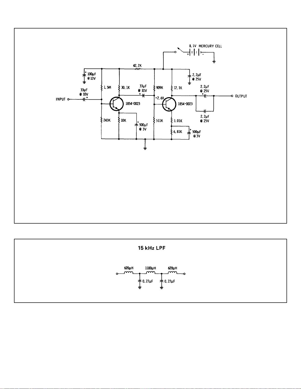
Figure 1-2. 40 dB Test Amlifier
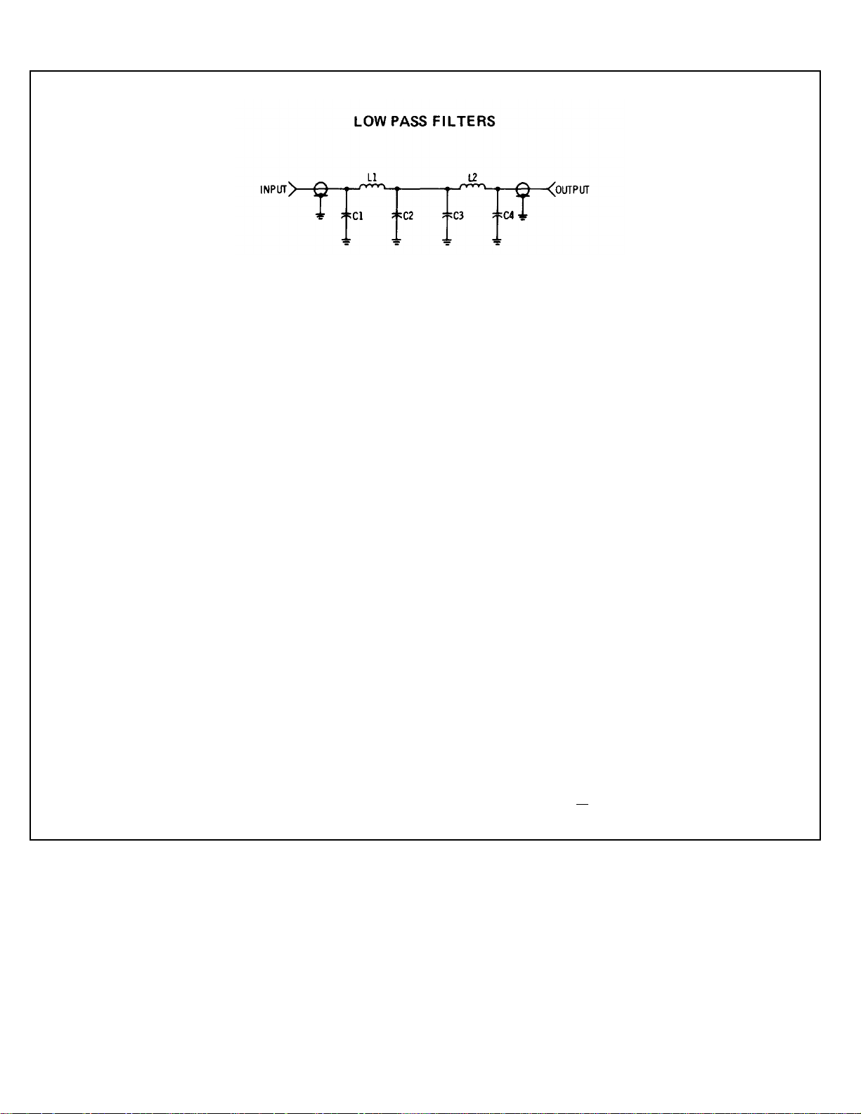
Figure 1-3. 15 kHz Low Pass Filter
1-11
Page 22
Section 1 TM 11-6625-2837-14&P-7
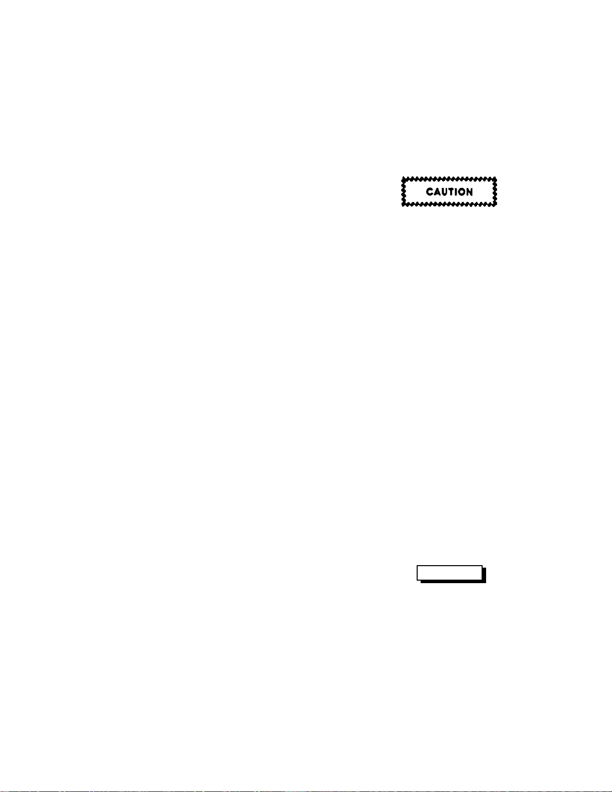
100 kHz - 50 ohms 100 kHz - 600 ohms
C1, C4 0.015 µF Mylar 0160-0194 C1, C4 1300 pF 0160-2221
C2 0.027 µF Mylar 0170-0066 C2 3000 pF 0160-2229
C3 0.022 µF Mylar 0160-0162 C3 1100 pF 0160-2219
L1, L2 100 µH 9140-0210 L1, L2 1200 µH 9100-1655
1 MHz -50 ohms 1 MHz - 600 ohms
C1, C4 1500 pF 0160-2222 C1, C4 130 pF 0140-0195
C2 3300 pF 0160-2230 C2 300 pF 0160-2207
C3 1600 pF 0160-2223 C3 120, µH 0140-0194
L1, L2 10H ±10% 9140-0114 L1, L2 120
5 MHz - 50 ohms 10 MHz - 50 ohms
C1, C2, C4 300 pF 0160-2207 C1, C4 150 pF 0140-0196
C3 680 pF 0160-3537 C2 330 pF 0160-2208
L1, L2 2 µH 9100-3345 C3 160 pH 0160-2206
L1, L2 1 µH±10% 9140-0096
NOTE
µ
9100-1637
Unless otherwise noted, tolerance of components is + 5%
and capacitors are mica. Part numbers are Hewlett-Packard
Figure 1-4. Low Pass Filters
1-12
Page 23
Section 2 TM 11-6625-2837-14&P-7
SECTION II
INSTALLATION
2-1. INTRODUCTION
2-2. This section provides information relative to initial
inspection, preparation for use, and storage and
shipment of the Model 86602B RF Section plug-in. Initial
Inspection provides instructions to be followed when an
instrument is received in a damaged condition.
Preparation For Use gives all necessary interconnection
and installation instructions. Storage and Shipment
provides instructions and environmental limitations
pertaining to instrument storage. Also provided are
packing and packaging instructions which should be
followed in preparing the instrument for shipment.
2-3. INITIAL INSPECTION
2-4. Inspect the shipping container for dam age. If the
shipping container or cushioning material is dam aged, it
should be kept until the contents of the shipment have
been checked for com pleteness and the instrument has
been checked mechanically and electrically. The
contents of the shipment s hould be as shown in Figure
1-1, and procedures for chec king electrical perform ance
are given in Section IV. If the contents are inc om plete, if
there is mechanical damage or defect, or if the instrument does not pass the electrical performance test,
notify the nearest Hewlett-Packard office. If the s hipping
container is damaged, or the c ushioning material shows
signs of stress, notify the carrier as well as the Hewlett-
Packard office. Keep the shipping m aterials for car rier’s
inspection. The HP office will arrange for repair or
replacement without waiting for claim settlement.
2-10. Modifications
2-11. A power supply modification to older versions of
Model 8660A and 8660B mainfram es are requir ed if they
are to be used with the option 002 RF Section.
Damage to the synthesized signal generator
system may result if an option 002 RF
Section is used with an older 8660A or 8660B
mainframe.
2-12. Due to the increased power consumption of the
option 002 instrument, mainframes with serial prefixes
1349A and below must be modif ied by installing a Field
Update Kit. For mainframe configurations other than
option 003 (60 Hz line operation), order kit number
08660-60273. For option 003 mainframes ( 50 - 400 Hz
line operation) order kit number 08660-60274.
NOTE
Verify that a new higher current fuse, HP Part
Number 2110-0365, 4A Slow Blow, is used in
mainframes with the power supply modification.
2-13. Operating Environment
2-14. The RF Section is designed to operate within the
following environmental conditions:
2-5. PREPARATION FOR USE
2-6. Power Requirements
2-7. All power required for operation of the RF Section
is furnished by the mainfram e. T his RF Section requir es
approximately 40 volt-amperes.
2-8. Interconnections
2-9. Prior to installing the RF Section plug-in into the
mainfram e, verify that the Frequency Extension Module
plug-in and interconnecting cable assem blies have been
installed in accordance with the instru ctions contained in
the Frequency Extension Module manual.
Temperature ........................................ 0° to +55°C
Humidity..................................... less than 95% relative
Altitude....................................... less than 15,000 feet
2-15. Installation Instructions
WARNING
The multi-pin plug connector which provides
interconnection from mainframe to RF
Section, will be exposed with the RF Section
removed from the right-hand mainframe
cavity. With the Line (Mains) Volt age off and
power cord disconnected, power supply
voltages may still remain which, if contacted,
may constitute a shock hazard.
2-1
Page 24
Section 1 TM 11-6625-2837-14&P-7
2-16. Insert the plug-in approximately half-way into the
right cavity of the mainframe. Rotate the latch (lower
right corner) to the left until it protrudes perpendicular to
the front panel. Refer to Figure 2-1, which shows the
plug-in partially inserted into the mainfram e and the latc h
rotated to a position that is perpendicular to the plug-in
front panel. Push the plug-in all the way into the
mainframe cavity and then rotate the latch to the right
until it snaps into position.
2-17. STORAGE AND SHIPMENT
2-18. Environment
2-19. The storage and shipping environm ent of the RF
Section should not exceed the following limits:
Temperature................................ 40° to +75°C
Humidity....................................... less than 95% relative
Altitude......................................... less than 25,000 feet
2-20. Packaging
2-21. Original Type Packaging. Containers and
materials identical to those used in f ac tor y pack aging are
available through Hewlett-Packard offices. If the
instrument is being returned to Hewlett-Packard for
servicing, attach a tag indicating the type of service
required, return address, model number, and full serial
Figure 2-1. RF Section Partially Inserted into Mainframe
number. Also mark the container FRAGILE to assure
careful handling. In any correspondence, refer to the
instrument by model number and full serial number.
2-22. Other Packaging. The following general
instructions should be used for re-packaging with
commercially available materials:
a. Wrap the instrument in heavy paper or
plastic. (If shipping to a Hewlett-Packard office or
service center, attach a tag indicating the type of ser vice
required, return address, model number, and full serial
number.)
b. Use a strong shipping container. A doublewall carton made of 350-pound test material is adequate.
c. Use enough shock-absorbing material (3 to 4inch layer) around all the sides of the instrument to
provide firm cushion and prevent movement inside the
container. Protect the control panel with cardboard.
d. Seal the shipping container securely.
e. Mark the shipping container FRAGILE to
assure careful handling.
Figure 2-1. RF Section Partially Inserted into Mainframe
2-2
Page 25

Section 3 TM 11-6625-2837-14&P-7
SECTION III
OPERATION
3-1. INTRODUCTION
3-2. This section contains information which will enable
the operator to learn to operate and quickly check for
proper operation of the RF Section plug-in as part of the
Synthesized Signal Generator System.
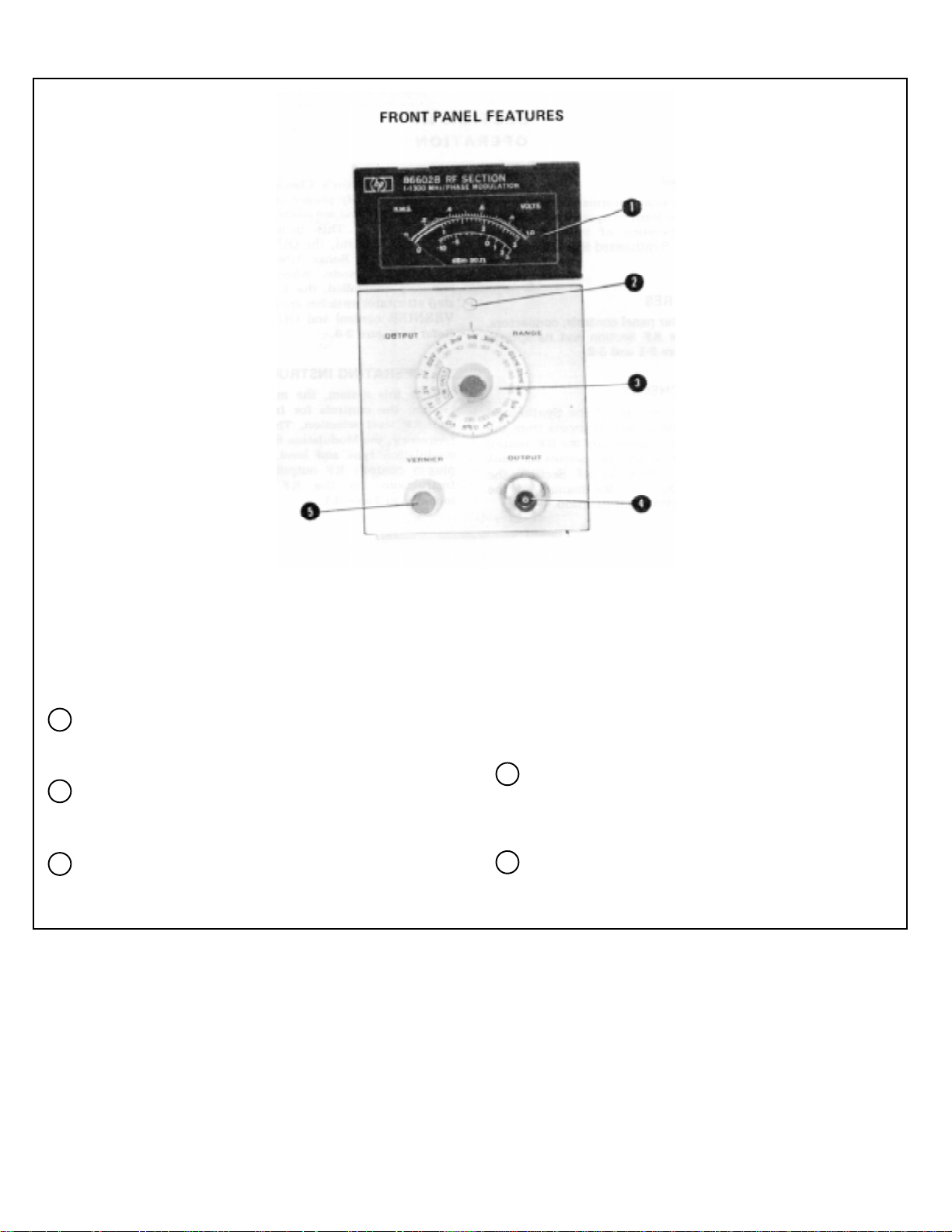
3-3. PANEL FEATURES
3-4. The front and rear panel controls, connectors , and
indicators of the RF Section and its options are
described by Figure 3-1 and 3-2.
3-5. OPERATOR’S CHECKS
3-6. The RF Section, as part of the Synthesized Signal
Generator System, accepts inputs from the rest of the
system but controls only the RF output level. Even
though the controlled circuits for most other functions are
within the RF Section, the actual checks are f ound in the
manual of the instrument which controls that function.
3-7. The Operator’s Check s in this m anual are intended
to verify proper operation of the circuits which control and
are controlled by the RF output level controls. This
includes the meter, the VERNIER control, the OUT PUT
RANGE switch, and the Output Range Attenuator when
operating in the local mode. W hen the system is being
remotely controlled, the 1 dB and 10 dB remote step
attentator switches are checked in place of the VERNIER
control and OUTPUT RANGE switch. Refer to Figure 3-
3.
3-8. OPERATING INSTRUCTIONS
3-9. In this system, the mainframe and plug-ins contain
the controls for frequency, modulation, and RF level
selection. The mainframe controls frequency, the
Modulation Section plug-in controls m odulation type and
level, and the RF Section plug-in controls RF output
level. The Operating Instructions for the RF Section
plug-in are included in Table 3-1.
3-1
Page 26
Section 3 TM 11-6625-2837-14&P-7
The front panel of the option 002 instrument is shown.
The standard instrument does not have the term PHASE
MODULATION after 1-1300 MHz. The option 001
instrument has an OUTPUT RANGE switc h whic h s hows
only the +10 and 0 dBm ranges.
1 Meter. Indicates the RF Output level in Vrms and
dBm (50w) with the scale reference indicated by the
OUTPUT RANGE switch.
2 Mechanical Meter Zero Control. Sets the Panel
Meter indicator to zero when the mainfram e LINE Switch
is set to STBY.
3 OUTPUT RANGE Switch. Sets the output level
range of all except option 001 instruments from
Figure 3-1. Front Panel Controls, Connectors, and Indicators
NOTE
+10 to -140 dBm (502) in 10 dB steps. For option 001
instruments, +10 and 0 dBm ranges only.
4 OUTPUT Jack. Type-N female coaxial connector.
RF Output level +10 to -146 dBm (0.7 Vrms to 0.01
/IVrms) into a 50Q load. Frequency range is 1 to
1299.999 999 MHz in 1 Hz steps.
5 VERNIER Control. RF Output continuously var-iable
within the useable range (+3 to --6 dB) as indicated by
the meter.
3-2
Page 27
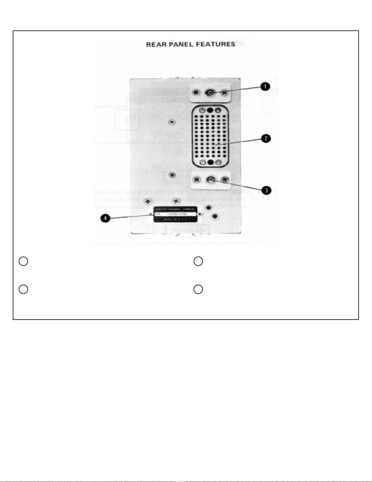
Section 3 TM 11-6625-2837-14&P-7
1 Coaxial Plug. Connects the 3.95 to 2.75 GHz RF
Input signal to the RF Section from the Frequency
Extension Module.
2 Interconnect Plug. Provides interconnection of
power supply voltages; RF and control signals between
the RF Section plug-in and the Main-frame, Frequency
Extension Module, and Modulation Section plug-in.
Figure 3-2. Rear Panel Connectors and Indicators
3 Coaxial Plug. Connects the 3.95 to 4.05 GHz LO
Input signal to the RF Section plug-in from the Frequency
Extension Module.
4 Serial Number Plate. Metal plate with stamped
serial number. Four-digit and letter f or prefix. Suffix is
unique to an instrument.
3-3
Page 28

Section 3 TM 11-6625-2837-14&P-7
WARNING
BEFORE CONNECTING TH IS SYSTEM TO LINE (MAINS) VOLTAGE,
the safety and installation instructions found in Sections II and III of the
mainframe manual should be followed.
Damage to the signal generator system may occur if option 002 RF
Sections are used with unmodified 8660A and 8660B main f rames with
serial prefixes 1349A and below. See the paragraph entitled
Modifications in Section II.
Refer to Section HI for RF Section Installation instructions.
1. Set the System controls as follows:
Mainframe
LINE Switch.................................................................................... ON
REFERENCESELECTOR.............................................................. EXT
CENTER FREQUENCY................................................................. 500 MHz
Modulation Section plug-in
MODE Switch................................................................................. OFF
RF Section plug-in
OUTPUT RANGE Switch ............................................................... 0 dBm
VERNIER Control........................................................................... +3 dB meter reading
NOTE
Figure 3-3. Operator’s Checks (1 of 2)
3-4
Page 29

Section 3 TM 11-6625-2837-14&P-7
OPERATOR’S CHECKS
2. Connect the RF Section OUTPUT to the power sensor input. Ver if y that the amplitude of the 500 MHz s ignal
is approximately +3 dBm.
3. Set the OUTPUT RANGE Switch to +10 dBm and adjust the VERNIER control for a -3 dB meter reading.
Verify that the output level is approximately +7 dBm.
4. Connect the RF Section OUTPUT to the frequenc y counter input through the 3 dB attenuator. Verify that the
signal is accurate within +1 Hz.
5. To check the remote control capabilities of the RF Section, connect a control unit to the m ainfram e. Repeat
steps 1 through 4 while the system is remotely programmed fr om an external source. Application Note 164-1
"Programming the 8660A/B Synthesized Signal Generator" provides the inform ation needed for r emote BCD
operation of this system. Application Note 164-2 "Calculator Control of the 8660A/B/C Synthesized Signal
Generator" provides the inform ation needed for calculator control of the s ystem us ing the HP- IB ( option 005).
Section III of the mainframe manual contains the same information in abridged form.
Figure 3-3. Operator’s Checks (2 of 2)
3-5
Page 30
Section 3 TM 11-6625-2837-14&P-7
Table 3-1. Operating Instructions (1 of 2)
OPERATING INSTRUCTIONS
TURN ON
BEFORE CONNECTING THIS SYSTEM TO THE LINE (MAINS)
VOLTAGE, the safety and installation instructions found in Sections
II and III of the mainframe manual should be followed.
Damage to the signal generator system may occur if option 002 RF
Sections are used with unmodified 8660A and 8660B main- frames
with serial prefixes 1349A and below. See the paragraph entitled
Modifications in Section II.
NOTE
Refer to Section II for RF Section Installation Instructions.
1. Set the mainf ram e’s LINE Switch to ON and the rear panel REFERENCE SELECTOR Switch to INT . Wait for the
mainframe "oven" indication to go out.
FREQUENCY SELECTION
2. Refer to Section III of the mainframe operating and service manual for information on system frequency selection.
RF OUTPUT LEVEL
3. dBm . Set the OUTPUT RANG E switch to within +3 and --6 dB of the desired output level. Adjust the VERNIER
control for a meter r eading which when added to the O UT PUT RANGE switch indication equals the desired output
level.
4. VOLTS. To set the RF output level in rms volts, the OUTPUT RANGE switch selec ted the f ull s c ale meter reading
and the VERNIER control is adjusted for the cor rect voltage reading on the meter. The voltage level f or meter
scale 1.0 should not be set below 0.32 of full scale. T he voltage level should not be set below 1 when using the
meter scale of 3.
NOTE
In order to achieve the output level accuracy specified, the level
selected must be S<+10 dBm and the RF Section front panel meter
reading must be as stated above.
5. Connect the RF Output to the Devic e Under Test. The front panel m eter r eading of RF Output level will be c or rec t
only if the input impedance of the Device Under Test is 50w2.
3-6
Page 31

Section 3 TM 11-6625-2837-14&P-7
Table 3-1. Operating Instructions (2 of 2)
MODULATION SELECTION
6. Refer to Section III of the Modulation Section plug-in operating and service manual for information relating to
selection of modulation type and level.
REMOTE OPERATION
7. Application Note 164-1 "Programming the 8660A/B Synthesized Signal Generator" provides most of the
information needed for remote BCD operation of this system. AN 164-2 "Calculator Control of the 8660A/B/C
Synthesized Signal Generator" provides information for r emote HP-IB operation of this system. In abridged f orm,
Section III of the mainframe manuals contain the same information.
3-7
Page 32

Section 4 TM 11-6625-2837-14&P-7
SECTION IV
PERFORMANCE TESTS
4-1. INTRODUCTION
4-2. The procedures in this section test the
instrument’s electrical performance using the
specifications of Table 1-1 as the per formance standard
All tests can be perform ed without access to l interior of
the instrument. A simpler operation test is included in
Section III under Operator’s Checks.
4-3. EQUIPMENT REQUIRED
4-4. Equipment required for the per formance tests is
listed in the Recommended Test Equipment table in
Section I. Any equipment that satisfies critical
specifications given in the table m ay substituted for the
recommended model(s).
4-5. TEST RECORD
4-6. Results of the perform ance tests may tabulated
on the Test Record at the end of the procedures. T he
Test Record lists all of the test specifications and their
acceptable limits. Test results recorded at incoming
inspection can be used for comparison in periodic
maintenance and trouble-shooting, and after repairs or
adjustments.
4-7. PERFORMANCE TESTS
4-8. For each test, the specifications are written
exactly as they appear in the specification table in
Section I. Next, a description of the test and any special
instructions or problem areas are included. Most tests
that require test equipment have a setup drawing; each
has a list of required equipment. The initial steps of each
procedure give control settings required for that
particular list.
To avoid the possibility of damage to the
instrument or test equipment, read
completely through each test before starting
it. Then make any preliminary control
settings before continuing with the
procedure.
4-1
Page 33

Section 4 TM 11-6625-2837-14&P-7
PERFORMANCE TESTS
4-9. FREQUENCY RANGE
SPECIFICATION:
1 to 1299.999999 MHz selectable in 1 Hz steps. Frequencies from 200 to kH z to 1 MHz m ay also be selec ted with som e
degradation in specifications.
DESCRIPTION:
The Synthesized Signal Generator System RF OUTPUT is monitored by a frequency counter which supplies a common
time base reference signal. The frequencies are checked at the extremes. Any specified frequency may be checked.
Figure 4-1. Frequency Range Test Setup
EQUIPMENT:
Frequency Counter....................................HP 5340A
10 dB Fixed Attenuator..............................HP 8491A Opt 003
NOTE
In the following procedure, allow for accuracy of counter used. -Model
recommended is specified at +1 count.
1. Connect frequency counter 10 MHz output reference signal to mainframe EXT REF input as shown in Figure 4-1
and set mainframe rear panel REF switch to EXT.
2. Set the RF Section OUTPUT RANGE switch to 0 dBm; set the VERNIER control full CW.
3. Set mainframe center frequency to 1.000 000 MHz and check RF section output frequency with counter. Record
the frequency.
0.999999_______________________1.000001 MHz
4. Set m ainf ram e center f requenc y to 1299.999 999 MHz (Option 004 mainf ram e set to 1299.,s pace 9999 MHz) and
check RF Section output frequency with counter. Record the frequency.
1299.999 998________________1300.000 000 MHz
4-2
Page 34

Section 4 TM 11-6625-2837-14&P-7
PERFORMANCE TESTS
4-10. FREQUENCY ACCURACY AND STABILITY
SPECIFICATION:
CW f requenc y accuracy and long term stability are determ ined by the aging rate of the time base (internal or external) and
its sensitivity to changes in temperature and line voltage. Internal ref er enc e osc illator acc ur ac y = + aging rate +3 x 10⁻¹⁰/°
C + 3 x 10⁻¹⁰/1% change in line voltage. (Aging rate for the tim e base in the standard mainfram e is 3 x 10- 8/day; for
option 001 mainframes, 3 x 10⁻⁹/day.)
NOTE
If there is any reason to doubt the mainframe crystal oscillator
accuracy or stability, r efer to the per formanc e tes t in Sec tion IV of
the mainframe manual.
_______________________________________
4-11. FREQUENCY SWITCHING TIME
SPECIFICATION:
6 ms to be within 50 Hz of any new frequency selected; 100 ms to be within 0.5 Hz of any new frequency selected.
DESCRIPTION:
A change in the Synthesized Signal Generator System's frequency is remotely programmed; af ter a preset time interval
the frequency is measured. A trigger pulse from the program m ing device is f irst c oupled to the oscillos cope. T he pulse is
delayed a preset interval by the oscilloscope and then coupled to the computing counter at which tim e the frequency is
measured.
NOTE
The frequencies in this test were selected for worst-case
conditions (longest switching time).
4-3
Page 35

Section 4 TM 11-6625-2837-14&P-7
PERFORMANCE TESTS
4-11. FREQUENCY SWITCHING TIME (Cont’d)
Figure 4-2. Frequency Switching Time Test Setup
EQUIPMENT:
DC Power Supply.......................................HP 721A
Computing Counter....................................HP 5360A/5365A
Marked Card Programmer.........................HP 3260A Opt 001
Oscilloscope...............................................HP 180C/1801A/1821A
Coaxial Tee................................................HP 1250-0781
PROCEDURE:
1. Connect the dc power supply +5 volt output through a 1000 ohm resistor to pin 17 of the m ating connector f or J3.
Pin 17 (flag) of the Marked Card Programmer output connector is also connected to the oscilloscope ext trigger
input.
2. Connect the marked card programmer to mainframe rear panel connector J3.
3. Connect oscillos cope delayed sweep output through a BNC TEE to oscilloscope channel A vertical input and to
computing counter rear panel external time measurement input.
4. Set counter controls as f ollows: rear panel switch to trigger ; "B" channel to X1 sensitivity; m odule switch pres sed;
digits displayed for necessary resolution; measurement time to 1; counter gate time to 1 ms.
5 Program the System for 29.999 999 MHz. Set the mainframe rear panel reference switch to external.
6. Set oscilloscope controls as follows: trigger to ac slow; ext, negative slope, trigger level at about 9:00 o’clock;
sweep mode auto; delay trigger auto; main sweep 1 ms; delay sweep 0.1 ps; main sweep mode.
7. Set oscilloscope trace to start at left vertical graticule line. Use oscilloscope delay control to delay spike 5.5
divisions from CRT left graticule line.
8. Switch oscilloscope sweep mode from auto to normal.
4-4
Page 36

Section 4 TM 11-6625-2837-14&P-7
PERFORMANCE TESTS
4-11. FREQUENCY SWITCHING TIME (Cont’d)
9 Program the system for 30.000 000 MHz. Frequency displayed on computing counter should be 30 MHz + 50 Hz.
Record the frequency.
29.999950__________________30.000050 MHz
10. Program the system for 29.999 999 MHz. Frequency displayed on counter should be within + 50 Hz of 29.999 999
MHz.
29.999949__________________30.000049 MHz
11. Set Oscilloscope normal sweep for 10 ms and delay sweep to 1 us.
12. Set Oscilloscope sweep mode to auto and delay control for delay spike 9.5 divisions from the CRT left graticule
line.
13. Set Oscilloscope main trigger to normal and computing counter gate time to 10 ms.
14. Program the System for 30.000 000 MHz. Frequency displayed on computing counter should be within + 5 Hz or
programmed frequency.
29.999995__________________30.000005 MHz
15. Program the System for 29.999 999 MHz. Frequency Displayed on computing counter should be within + 5 Hz of
programmed frequency.
29.999994___________________30.000004 MHz
NOTE
To reduce the effect of random errors, steps 5 thr ough 10 and 13 through
15 may be repeated several times (5 minimum). Record the average
frequency.
______________________________________________
4-12. OUTPUT LEVEL SWITCHING TIME
SPECIFICATION:
In remote mode, any level change can be accom plished in less than 50 ms. Any change to another level on the same
attenuator range can be accomplished in 5 ms.
DESCRIPTION:
The Synthesized Signal Generator System RF OUTPUT level (attenuation) is remotely programmed while the RF
OUTPUT is detected and monitored by an oscilloscope. Because the oscilloscope is triggered by the programming
device, the time needed to effect the level change may be measured directly on the oscilloscope CRT.
4-5
Page 37

Section 4 TM 11-6625-2837-14&P-7
PERFORMANCE TESTS
4-12 OUTPUT LEVEL SWITCHING TIME (Cont’d)
Figure 4-3. Output Level Switching Time Test Setup
EQUIPMENT:
Marked Card Programmer...................................... HP 3260A Opt 001
Oscilloscope............................................................ HP 180C/1801A/1821A
Crystal Detector ..................................................... HP 8471A
Power Supply.......................................................... HP 721A
PROCEDURE:
1. Connect equipm ent as illustrated in Figure 4-3. Note that + 5 volt output from DC Power Supply is connected
through a 1000 ohm resistor to pin 17 of mating connector to J3 and to Oscilloscope external trigger input.
2. Connect RF Section OUTPUT through crystal detector to oscilloscope Channel A input.
3. Set Oscillos cope controls as follows: Main Tim e/Div, 5 ms; Vertical input, dc coupled, 0.2 V/Div; Norm al Sweep;
Ext Trigger, negative slope, AC slow Trigger level about 9:00 o’clock.
4. Program the System’s center f requency for 500 MHz and 10 dB attenuation of the RF output signal. Reprogram
for 19 dB attenuation. Switching time should be less than 5 ms. Record switching time.
10 to 19 dB_______________________5 ms
5. Program RF Section attenuation for 10 dB, then for 30 dB. Switching time should be less than 50 ms.
10 to 30 dB_______________________50 ms
4-6
Page 38

Section 4 TM 11-6625-2837-14&P-7
PERFORMANCE TESTS
4-12. OUTPUT LEVEL SWITCHING TIME (Cont’d)
6. Repeat steps 4 and 5 with center frequency set to 1 MHz.
10 to 19 dB__________________________5 ms
_______________________________________________
4-13A. OUTPUT ACCURACY
SPECIFICATION: (for local and remote modes)
+1.5 dB to -76 dBm; +
DESCRIPTION:
The RF level accuracy for the +10 and 0 dBm ranges is measured with a power meter. For the lower ranges, an IF
substitution measurement technique is used.
2.0 dB to -146 dBm at meter readings between +3 and -6 dB.
RF level (attenuation) measurements using IF substitution is accomplished by 1) converting the RF output to a low
frequency IF signal, 2) offsetting the decrease in RF level ( increas e in attenuation) by an equal decrease in IF attenuation.
This maintains a fairly constant output level at the IF load. The intermediate frequency is selected on the basis of
availability of a precision attenuator. Therefore, any variation in output level from an established r eferenc e is pr im arily due
to the RF attenuator.
4-7
Page 39

Section 4 TM 11-6625-2837-14&P-7
PERFORMANCE TESTS
4-13A. OUTPUT ACCURACY (Cont’d)
EQUIPMENT:
Figure 4-4A. Output Accuracy Test Setup
Power Meter/Sensor............................................... HP 435A/8481A
Synthesized Signal Generator ............................... HP 8660C/86602B/86631B
40 dB Attenuator..................................................... HP 8491A Option 040
Mixer....................................................................... Watkins-Johnson M1J
4 MHz Low Pass Filter............................................ CIRC-Q-TEL FLT/21B-
4-3/50-3A/3B
Coaxial Tee............................................................. 1250-0781 (BNC)
50 Ohm Termination............................................... HP 11593A
40 dB Amplifier........................................................ (See Figure 1-2)
Double Shielded Cables (5 required)...................... HP 08708-6033
Capacitor, 100 #F ................................................... .HP 0180-2207
Resistor, 100 k........................................................ HP 0698-7284
Type N-to SMA Adaptor.......................................... OSM 21040
SMA-to-OSM Right Angle Adapter ......................... OSM 219
SMA-to-BNC Adapter (2)........................................ OSM 21190
10 dB Step Attenuator............................................. HP 355D Option H38
Wave Analyzer........................................................ HP 3581A
4-8
Page 40

Section 4 TM 11-6625-2837-14&P-7
PERFORMANCE TESTS
4-13A. OUTPUT ACCURACY (Cont’d)
PROCEDURE:
1. Set the System Under Test Controls for a center frequency of 1000.000000 MHz and an output level of +10 dBm.
2. Set the power meter controls for the +15 dBm range.
3. Connect the power sensor to the RF Section OUTPUT jack of the System Under Test.
4. Set the RF Section c ontrols as shown in the table below and verify that the RF output level is within the specif ied
tolerance.
Synthesized Signal Generator System
OUTPUT RANGE
Switch
(dBm)
+10 0 +8.5________+11.5
+10 -3 +5.5________+ 8.5
+10 -6 +2.5________+ 5.5
0 -6 -7.5_________- 4.5
0 -3 -4.5_________- 1.5
0 0 -1.5_________+ 1.5
0 +3 +1.5_________+ 4.5
Panel Meter
Reading
(dB)
Power Reading
Reading
(dBm)
NOTE
Be careful not to vary the RF Section ‘s VERNIER control setting
throughout the rest of this procedure.
5. Connect the 40 dB attenuator directly to the OUTPUT jack of the RF Section in place of the power sensor.
6. Connect the “R” port of the mixer directly to the 40 dB attenuator using the Type N-to SMA adapter and the SMA-
to-OSM right angle adapter.
7. Connect the 4 MHz Low Pass Filter to the “I” port of the mixer with a SMA-to-BNC adapter.
8. Connect the cable from the Reference System output to the “L” port of the mixer with a SMA-to-BNC adapter.
NOTE
Be sure all connections are tight to prevent RF leakage.
9. Set the reference system c ontrols for a center frequency of 1000.011000 and an output level of +7 dBm . Set the
rear panel reference selector to external.
10. Set the 10 dB Step Attenuator to 50 dB.
4-9
Page 41

Section 4 TM 11-6625-2837-14&P-7
PERFORMANCE TESTS
4-13A. OUTPUT ACCURACY (Cont’d)
11. Set the wave analyzer controls as follows: frequency 11 kHz, resolution bandwidth 3 Hz, sweep mode of f, dBv/LIN
- dBm 600:1 switch to dBv/LIN, amplitude reference level -40 dB, AFC switch unlock and scale 10 dB.
12. Connect the other equipment which follows the 4 MHz Low Pass Filter as shown in Figure 4-4A.
13. Tune the wave analyzer frequency control for the maxim um m eter reading. Adj ust the input s ensitivity and vernier
controls for a midscale meter reading. Press the AFC control for frequency lock.
14. Wait 30 seconds for the DVM reading to stabilize. Record the DVM reading. This is the reference level equivalent
to the last power meter reading ( +3 dBm).
15. Use the following formula to calculate the obsolute RF output level from the System Under Test:
dBm = dBm1 -A dB +2(V-Vre
ff
dBm is the RF output level
dBm1 is the actual RF level measured at the +3 dBm (O dBm OUTPUT RANGE setting) in Step 4.
A dB is the difference in 10 dB step attenuator setting.
V is the DVM reading for each individual OUTPUT RANGE.
Vref is the reference DVM reading.
NOTE
The wave analyzer recorder output sensitivity is 2dB/volt.
16. Set the RF Section OUTPUT RANGE switch to -10 dBm; set the 10 dB step attenuator to the 40 dB. Wait 30
seconds for the reading to stabilize. Record the DVM reading in the table following step 17. Calc ulate and record
the RF level in the table.
EXAMPLE:
dBm = dBm1 --(∆dB) +2 (V1 -Vref)
dBm1 = 2.8 dBm
∆
dB = 10 dB
V1= 2.388 Vdc
Vref = 2.433 Vdc (from step 14)
dBm = 2.8 - (10) +2(2.388-2.433)
= 2.8 -10 +2(-0.045)
= -7.29 dBm
4-10
Page 42

Section 4 TM 11-6625-2837-14&P-7
PERFORMANCE TESTS
4-13A. OUTPUT ACCURACY (Cont’d)
17. Continue as in step 16,space to measure, record and calculate the DVM reading and RF level for each OUTPUT
RANGE setting as shown in the following table.
Absolute RF Output
Output Range 10dB Step DVM Level (dBm)
Switch Attenuator Reading
(dB) (Vdc) Min. Actual Max.
0 50 _________ + 1.5 __________ + 4.5
- 10 40 _________ - 8.5 __________ - 5.5
-20 30 _________ -18.5 __________ -15.5
-40 10 _________ -38.5 __________ -35.5
-50 0 _________ -48.5 __________ -45.5
18. Set the 10 dB step attenuator to 50 dB.
19. Remove the 40 dB attenuator and connect the mixer directly to the OUTPUT jack of the system under test.
20. Increase the wave analyzer’s input sensitivity by 10 dB. If necessary,space adjust the input sensitivity vernier for a
midscale meter reading.
21. Transfer the last calculated RF output level on the preceding table to the first line on the following table. Wait 30
seconds and record the new DVM reading (Vref).
22. Use the formula and the new Vref level to calculate the RF level for each range shown in the following table.
Absolute RF Output
Output Range 10 dB Step DVM Level (dBm)
Switch (dBm) Attenuator Reading
(dB) (Vdc) Min. Actual Max.
-50 50 ________ -48.5 ________ -45.5
-60 40 ________ -58.5 ________ -55.5
-70 30 ________ -68.5 ________ -65.5
-80 20 ________ -79.0 ________ -75.0
-90 10 ________ -89.0 ________ -85.0
-100 0 ________ -99.0 ________ -95.0
23. Set the wave analyzer’s AFC switch to unlock (OFF). Adjust the frequency control for the peak reading equal to
the last recorded DVM reading on the previous table.
24 Set the 10 dB step attenuator to 30 dB.
4-11
Page 43

Section 4 TM 11-6625-2837-14&P-7
PERFORMANCE TESTS
4-13A. OUTPUT ACCURACY (Cont’d)
25. Set the wave analyzer amplitude reference level to -60 dB. Increase the input sensitivity 10 dB.
26 Transf er the last RF output level reading on the preceding table to the first line of the following table. After 30
seconds record the new DVM reference on the first line of the following table.
27. Measure, calculate,space and r ecor d the DVM reading and RF level for each OUTPUT RANGE Setting as shown
in the following table. Due to the high noise levels evident on this test, ther e is apprec iable deviation in the wave
analyzer and DVM readings. Record the average reading.
Absolute RF Output
Output Range 10dB Step DVM Level (dBm)
Switch (dBm) Attenuator Reading
(dB) (Vdc) Min. Actual Max.
-100 30 _______ -99.0 _________ -95.0
-110 20 _______ -109.0 _________ -105.0
-120 10 _______ -119.0 _________ -115.0
-130 0 _______ -129.0 _________ 125.0
NOTE
Output level accuracy may be checked at any frequency between 300
and 2000 MHz using this procedure. This procedure may also be used at
the frequency extremes if a well shielded mixer specified for the desir ed
frequency range is used in place of the Watkins Johnson M1J.
4-13B. OUTPUT ACCURACY - ALTERNATE PROCEDURE
SPECIFICATION:
+1.5 dB to -76 dBm; +2.0 dB to -146 dBm at meter readings between +3 and -6 dB.
DESCRIPTION:
The RF Level Accuracy for the +10 and 0 dBm ranges is m easured with a power m eter. A reference level is es tablished
and accuracy is checked from 0 dBm to -80 dBm by compar ing the RF Sec tion attenuation agains t a calibr ated 10 dB s tep
attenuator.
NOTE
This procedure checks all sections of the RF Section Attenuator
separately. Also, the 10 dB, 20 dB, and 40 dB sections are checked in all
possible combinations. The sum of the -70 dBm inaccuracy at -80 dBm
shall not exceed +1.0 dB.
4-12
Page 44

Section 4 TM 11-6625-2837-14&P-7
PERFORMANCE TESTS
4-13B. OUTPUT ACCURACY - ALTERNATE PROCEDURE (Cont’d)
Figure 4-4B. Output Accuracy Test Setup (Alternate Procedure)
EQUIPMENT:
Spectrum Analyzer.................................................. HP 8555A/8552B/140T
Power Meter/Sensor............................................... HP 435A/8481A
10 dB Step Attenuator............................................. HP 355D Option H38
20 dB Amplifier........................................................ HP 8447A
PROCEDURE:
1. Set the system controls for a frequency of 30 MHz and an output level of +10 dBm.
2. Connect the power sensor to the RF Section’s OUTPUT jack.
3. Set the RF Output Level as shown in the table below and verify that the level is within the specified tolerance.
Synthesized Signal Generator System
Output Range
Switch
(dBm)
+10 0 +8.5_______+11.5
+10 -3 +5.5_______+ 8.5
+10 -6 +2.5_______+ 5.5
0 -6 -7.5________-4.5
0 -3 -4.5________-1.5
0 0 -1.5________+1.5
0 +3 +1.5________+4.5
Panel Meter
Reading
(dB)
Power Meter
Reading
(dBm)
4-13
Page 45

Section 4 TM 11-6625-2837-14&P-7
PERFORMANCE TESTS
4-13B. OUTPUT ACCURACY - ALTERNATE PROCEDURE (Cont’d)
NOTE
Do not change the RF Section VERNIER Control Setting until this
procedure is completed.
4. Set the spectrum analyzer controls as follows: center frequency 30 MHz, frequency span per division 5 kHz,
resolution bandwidth 3 kHz, input attenutation 10 dB, vertical sensitivity per division 2 dB and sweep time per
division 5 ms.
5. Set the 10 dB Step attenuator switch to the 80 dB range.
6. Connect the equipment as shown in Figure 4-4B.
7. Adjust the reference level range and vernier to extablish a reference level on the analyzer display.
8. On the first line of the following table, record the power meter reading shown on the preceding table for the
OUTPUT RANGE Setting of 0 dBm and the panel meter reading of +3 dB. T his is the absolute RF level which
corresponds to the display reference.
9. Set the OUTPUT RANGE switch and the 10 dB step attenuator range s witch s ettings as s hown on each line of the
following table. Record the display variation from the established reference.
10. Calculate the RF level using the following formula:
dBm = dBm1 - ∆AdB10 + ∆dB
dBm is the RF output level
dBm1 is the RF level measured at +3 dBm (0 dBm OUTPUT RANGE setting) in step 3.
∆
∆
is the change in 10 dB Step Attenuator level
dB
10
dB is the variation from the established display reference for each OUTPUT RANGE setting.
For example, results of the first step are:
dBm1 =+2.8
10
= 10
∆
A dB
∆
A dB= -0.2
dBm = +2.8 dBm -10 dB +(-0.2) dB
= -7.4 dBm
4-14
Page 46

Section 4 TM 11-6625-2837-14&P-7
PERFORMANCE TESTS
4-13B. OUTPUT ACCURACY - ALTERNATE PROCEDURE (Cont’d)
10 dB Step RF Output Level
Output Range Attenuator (dBm)
Switch (dBm) (dB) Min. Measured Max.
0 80 + 1.5 ________ + 4.5
-10 70 -8.5 ________ - 5.5
-20 60 -18.5 ________ -15.5
-30 50 -28.5 ________ -25.5
-40 40 -38.5 ________ -35.5
-50 30 -48.5 ________ -45.5
-60 20 -58.5 ________ -55.5
-70 10 -68.5 ________ -65.5
-80 0 -79.0 ________ -75.0
11. Subtract the two levels obtained for OUTPUT RANGES of -70 and -80 dBm. The level change should be 10 + 1
dB.
9 dB_________________________________11 dB
4-14. OUTPUT FLATNESS
SPECIFICATION:
Output level variation with frequency is less than +1.0 dB from 1-1300 MHz at front panel meter readings between +3 and 6 dB.
DESCRIPTION:
After an output level reference is established, power level measurements are made at various frequencies across the
range of the Synthesized Signal Generator System. The Output levels must fall within the limits specified.
EQUIPMENT:
Power Meter/Sensor............................................... HP 435A/8481A
PROCEDURE:
1. Zero the Power Meter.
2. Set the system center frequency to 1000 MHz.
3. Set the Power Meter range switch to 0 dBm; set the RF Section OUTPUT RANGE Switch and VERNIER Control
for an output level of -1.0 dBm as read on the power meter.
4-15
Page 47

Section 4 TM 11-6625-2837-14&P-7
PERFORMANCE TESTS
4-14. OUTPUT FLATNESS (Cont’d)
4. Measure and record the power level indicated by the Power Meter at the following center frequencies: 1 MHz, 10
MHz, 100 MHz, 200,space 400,space 600,space 800,space and 1299 MHz.
1 MHz -2.0_______________0.0 dBm
10 MHz -2.0_______________0.0 dBm
100 MHz -2.0_______________0.0 dBm
200 MHz -2.0_______________0.0 dBm
400 MHz -2.0_______________0.0 dBm
600 MHz -2.0_______________0.0 dBm
800 MHz -2.0_______________0.0 dBm
1299 MHz -2.0_______________0.0 dBm
4-15. HARMONIC SIGNALS
SPECIFICATION:
All harmonically related signals are at least 30 dB below the desired output signal for output levels < +3 dBm. (25 dB down
for output levels above +3 dBm.)
DESCRIPTION:
A spectrum analyzer is used to measure the r elative levels of the second and third carrier har monics with respec t to the
carrier fundamental at various center frequencies.
EQUIPMENT:
Spectrum Analyzer.................................................. HP 8555A/8552B/140T
PROCEDURE:
1. Set the system center frequency to 1299 MHz; set the RF Section OUTPUT RANGE switch and VERNIER control
for an output level of +10 dBm.
2. Connect the power meter/sensor to the system RF OUTPUT jack.
3. Readjust the VERNIER control for a power meter reading of +10 dBm.
4. Set the spectrum analyzer input attenuation to 30 dB. Connect the RF Section OUTPUT jack to the spectrum
analyzer RF input.
5. Set the other spectrum analyzer controls for convenient viewing of the carrier. Adjust the controls as necessary to
view the second and third harmonics. Record the harmonic levels relative to the fundamental signal.
Second Third
1299 MHz >,space 25 dB down ______ ______
4-16
Page 48

Section 4 TM 11-6625-2837-14&P-7
PERFORMANCE TESTS
4-15. HARMONIC SIGNALS (Cont’d)
6. Repeat steps 1 through 5 at the other frequencies listed. Record the levels.
Second Third
1000 MHz>-25 dB down ______ ______
500 MHz>25 dB down ______ ______
100 MHz>25 dB down ______ ______
10 MHz >25 dB down ______ ______
7. Set the system center frequency to 100 MHz; set the RF Section OUTPUT RANGE switch to 0 dBm and the
VERNIER control for a front panel meter reading of +3 dB. Record the harmonic levels.
Second Third
100 MHz >-30 dB down ______ ______
4-16 PULSE MODULATION RISETIME
SPECIFICATION:
50 nanoseconds.
DESCRIPTION:
The external pulse generator output is coupled to the RF Section plug-in through the Model 86631B Auxiliary Section. The
pulse modulated signal is detected and the rise time measured with an oscilloscope.
4-17
Page 49

Section 4 TM 11-6625-2837-14&P-7
PERFORMANCE TESTS
4-16. PULSE MODULATION RISETIME (Cont’d)
Figure 4-5. Pulse Modulation Risetime Test Setup
EQUIPMENT:
Pulse Generator...................................................... HP 8013A
Oscilloscope............................................................ HP 180C/1801A/1821A
Crystal Detector...................................................... HP 423A
Termination, 50Ω Feedthru..................................... HP 11048C
Band Pass Filter...................................................... HP 8430A PROCEDURE:
1. Set System center frequency to 1200 MHz.
2. Set the RF Section OUTPUT RANGE switch and VERNIER control for an output of +10 dBm.
3. Set the Auxiliary Section external modulation switch to pulse; set pulse level control full cw.
4. Adjust pulse generator output for -10 Vpk (into 50Q) with risetime <10 ns; set pulse repetition rate and width to
convenient values.
5. Connect equipment as illustrated in Figure 4-5.
6. Adjust oscilloscope to display leading edge of detected pulse modulated RF signal. Risetime, as measured
between the 10% and 90% amplitude points on leading edge should be 50 nanoseconds or less.
__________________50 ns
4-18
Page 50

Section 4 TM 11-6625-2837-14&P-7
PERFORMANCE TESTS
4-17. PULSE MODULATION ON/OFF RATIO
SPECIFICATION:
At least 40 dB
DESCRIPTION:
An HP Model 86631B Auxiliary Section is inserted in the left cavity of the ma inframe. Inputs of -9.5Vdc (pulse-on) and 0
Vdc (pulse-off) are input to the Aux iliary Section while the RF output of the system is monitored by a s pectrum analyzer.
The ratio of the pulse-off and pulse-on RF levels is the on/off ratio.
EQUIPMENT:
Spectrum Analyzer.................................................. HP 8555A/8552B/140T
Power Supply.......................................................... HP 6215A
PROCEDURE:
1. Set System center frequency to 500 MHz, RF Section OUTPUT RANGE Switch and VERNIER control for an
output level of +10 dBm, and Auxiliary Section external modulation switch to pulse.
2. Set spectrum analyzer input attenuation to 30 dB; connect the RF Section OUTPUT to the analyzer RF input.
3. Connect -9.5 Vdc from the power supply to the Auxiliary Section input.
4. Adjust the analyzer controls for a CRT display of the carrier. Establish the reference by positioning the carrier
peak on the top horizontal graticule line.
5. Set the power supply output to 0.0 Vdc. Set the Pulse Level control fully clockwise. The signal displayed on
Spectrum Analyzer should be >40 dB down with respect to the reference. Record the displayed level.
40 dB down__________
4-18. AMPLITUDE MODULATION DEPTH AND 3 dB BANDWIDTH
SPECIFICATION:
Depth: 0-90% for RF output level meter readings from +3 to -6 dB and only at +3 dBm and below. 3 dB
Bandwidth: At center frequencies <10 MHz
10 kHz from 0 - 30% AM
6 kHz from 0 - 70% AM
5 kHz from 0 - 90% AM
At center frequencies >10 MHz
100 kHz from 0 - 30% AM
60 kHz from 0 - 70% AM
50 kHz from 0 --90% AM
NOTE
To check AM accuracy, refer to section IV of the appropriate modulation
section Operating and Service manual.
4-19
Page 51

Section 4 TM 11-6625-2837-14&P-7
PERFORMANCE TESTS
4-18. AMPLITUDE MODULATION DEPTH AND 3 dB BANDWIDTH (Cont’d)
DESCRIPTION:
The system Rf output is am plitude modulated. T he signal is demodulated by a peak detector in a spectr um analyzer (the
frequency span width is set to zero). The ac and dc com ponents are m easured with a voltmeter at the detector ( vertical)
output. First, the dc component is set to -283 mVdc plus a detector offset correction. Then, the ac component is
measured. The AM level (%) is ½ (one half) the rms output.
Because of the required measurement accuracy, the accuracy of the spectrum analyzer’s detector offset must be known to
+2 mVdc. The off set voltage is calculated by measuring the change in the detector output f or a change in the RF input
and assuming a linear detector over the range of the levels used.
EQUIPMENT:
Figure 4-6. Amplitude Modulation Depth and 3 dB Bandwidth Test Setup
Test Oscillator......................................................... HP 651B
AC Voltmeter........................................................... HP 403B
10 dB Step Attenuator............................................. HP 3550 Option H38
Spectrum Analyzer.................................................. HP 8555A/8552B/140T
Digital Voltmeter ..................................................... HP 34740A/34702A
Coaxial Tee (2 required)......................................... HP 1250-0781
Crystal Detector...................................................... HP 423A
Oscilloscope............................................................ HP 180C/1801A/1821A
Resistor 1K ............................................................ HP 0757-0280
4-20
Page 52

Section 4 TM 11-6625-2837-14&P-7
PERFORMANCE TESTS
4-18. AMPLITUDE MODULATION DEPTH AND 3 dB BANDWIDTH (Cont’d)
PROCEDURE:
1. Connect the equipment as shown in Figure 4-6 (step 1).
2. Set the synthesized signal generator controls as follows: center frequency 30 MHz, OUTPUT RANGE 10 dBm,
VERNIER control for a panel meter reading of 0 dB, and AM off.
3. Let the spectrum analyzer warm up for 1 hour to minimize drift of the spectrum analyzer detector output. Set 10
dB step attenuator to 10 dB attenuation.
4. Set the spec trum analyzer center frequency to 30 MHz, frequency span per division 5 MHz, resolution bandwidth
300 kHz; input attenuation to 20 dB, and vertical sensitivity per division 10 dB. Adjust the center frequency control
to center the display. Set the frequency span to zero and tune to peak the trace.
NOTE
Throughout this test, continually check that the signal is peaked for
maximum deflection. Tune the center frequency control for maximum
signal deflection.
5. Set the vertical scale to linear and adjust the reference level vernier for a digital voltmeter reading of 200 mVdc.
6. Set the 10 dB step attenuator to 0 dB and record the digital voltmeter reading.
_______________mVdc
7. Set the 10 dB Step Attenuator to 20 dB and record the digital voltmeter reading.
_______________mVdc
8. Calculate the offset voltage using the following formula:
mVdc + 200a
=
V
off
1-a
Where Voff is the offset voltage in millivolts
mVdc is the DVM reading in m illivolts a is 3.16
(step 5) or 0.316 (step 6).
For example:
mVdc = -687 in step 5
-687 + 200 (3.16
therefore V
= = +25.5 mVdc
off
)
1 -(3.16)
9. Find the value of V
.
V
off
for step 6. The difference between the two should be < 4 m Vdc. Use the average value of
off
10. Set the 10 dB step Attenuator to 10 dB.
4-21
Page 53

Section 4 TM 11-6625-2837-14&P-7
PERFORMANCE TESTS
4-18. AMPLITUDE MODULATION DEPTH AND 3 dB BANDWIDTH (Cont’d)
11. Set the system center frequency to 500 MHz, the modulation mode to AM, the modulation source to ex ternal, and
a modulation level of 30% (0.3 Vrm s input to an Auxiliary Section; 1.5 Vrms to a Modulation Section) at a 1 kHz
rate.
12. Set the spectrum analyzer center frequency control to 500 MHz, frequency span to zero, and peak the trace. Set
the reference level vernier for a digital voltmeter reading of -283 mVdc + Vof
See Steps 8 and 9.
f.
13. Set the DVM controls to measure the peak detector’s ac component. The modulation level (%) is 1/2 (one-half)
the DVM reading (Vrms). Record the reading for 30% AM.
50 mVrms_______________________70 mVrms
14. Set the modulation section (test oscillator) controls for 70% AM. Record the DVM reading.
130 mVrms_____________________150 mVrms
15. Set the modulation section (test oscillator) controls for 90% AM. Record the DVM reading
170 mVrms_____________________190 mVrms
16. Connect the crystal detector to the RF Section OUTPUT jack.
17. Set the modulation section and test oscillator controls for an AM level of 30% (0.3 Vrms input to an auxiliary
section; 1.5 Vrms to a modulation section) at a 5 kHz rate.
18. Set the oscilloscope controls for a 5 division peak-to-peak display of the demodulated signal.
19. Increase the test oscillator frequency to 100 kHz. The signal amplitude should be >3.5 divisions peak-to-peak.
3.5 div. p-p_________________
20. Install the 1500 Pf capacitor as shown in Figure 4-6.
21. Repeat steps 17 through 19 with center frequenc y set to 9 MHz. Increase the test os cillator frequenc y from 5 to
10 kHz. Record the signal amplitude.
3.5 div. p-p_________________
4-22
Page 54

Section 4 TM 11-6625-2837-14&P-7
PERFORMANCE TESTS
4-19. FREQUENCY MODULATION RATE AND DEVIATION
SPECIFICATION:
Rate: DC to 200 kHz with the 86632B or 86635A.
20 Hz to 100 kHz with the 86633B.
Maximum Deviation (Peak):
200 kHz with the 86632B and 86635A.
100 kHz with the 86633B.
NOTE
To check the frequency modulation rate and deviation, refer to the
performance test in Section IV of the applicable modulation section
manual.
4-20. OUTPUT IMPEDANCE AND VSWR
SPECIFICATION:
Impedance: 50
VSWR: <2.0 on +10 and 0 dBm ranges; <1.3 on -10 dBm range and below.
DESCRIPTION:
The Synthesized Signal Generator System’s output signal is reflected back into the RF OUT PUT j ack by a coaxial short at
the end of an adjustable stub (a variable length of air -line). This reflected s ignal is re-reflected by any mism atch at the
jack. The re-ref lected signal combines with the output signal according to the relative phase and m agnitude of the two
signals. The combined signal is monitored by a directional coupler and then measured by a voltmeter or spectrum
analyzer. Maximum and minimum power levels are noted as the electrical length of the stub is var ied (i.e. the electrical
distance from the RF OUT PUT jack to the coaxial short is varied). The maximum allowable change in voltage or dB is
calculated from the following formulas.
Ω
VSWR =Vmax
Vmin
Vmax = (VSWR) (Vmin)
dB = 20 log (Vmax)
(Vmin)
dB = 20 log (VSWR)
4-23
Page 55

Section 4 TM 11-6625-2837-14&P-7
PERFORMANCE TESTS
4-20. OUTPUT IMPEDANCE AND VSWR (Cont’d)
Figure 4-7. Output Impedance Test Setup
EQUIPMENT:
Directional Coupler ................................................. HP 778D Opt 12
Adapter (Male Type N to GR 874).......................... HP 1250-0847
Adjustable Stub....................................................... General Radio 874-D50L
Spectrum Analyzer ................................................. HP 8555/8552B/140T
5052 Termination.................................................... HP 11593A
PROCEDURE:
1. Set the Synthesized Signal Generator system center frequency to 500 MHz, the OUTPUT RANGE switch to +10
dBm, and the VERNIER control for a panel meter reading of 0 dB.
2. Set up the equipment as shown in Figure 4-7.
3. Set the spectrum analyzer controls for a convenient display of the signal. Set the vertical sensitivity to 2 dB per
division.
4. Adjust the stub for a minimum indication on the spectrum analyzer display. Adjust the reference level range and
vernier controls for a convenient reference level.
5. Adjust the stub for a maximum indication on the display. The signal level increase should be <6 dB (VSWR <2.0).
____________________6dB
6 Set the system’s OUTPUT RANGE switch to 0 dBm. Adjust the VERNIER control for a panel meter reading of +3
dB.
7 Repeat steps 3 and 4. The signal level increase should be <6 dB (VSWR <2.0).
____________________6dB
8. Set the system’s OUTPUT RANGE switch to -10 dBm.
4-24
Page 56

Section 4 TM 11-6625-2837-14&P-7
PERFORMANCE TESTS
4-20. OUTPUT IMPEDANCE AND VSWR (Cont’d)
9. Repeat steps 3 and 4. The signal level increase should be <2.3 dB (VSWR <1.3).
10. If desired, repeat at other frequencies between 100 MHz and 1 GHz.
___________________2.3 dB
NOTE
The steps given above effectively check VSWR at all settings of the
output attenuator.
4-21. SIGNAL-TO-PHASE NOISE RATIO
SPECIFICATION: (For AM,s CW, and OM modes only)
Greater than 45 dB in a 30 kHz band centered on the carrier and excluding a 1 Hz band centered on the carrier.
DESCRIPTION:
AC voltage measurements proportional to carrier amplitude and residual carrier phase deviation are compared for the
signal-to-phase noise ratio. The Synthesized Signal Generator System’s reference and RF output (carrier) signals are
mixed and the difference frequency is monitored by an oscilloscope and ac voltmeter. T he mixer output (proportional to
the carrier amplitude) is noted. The two signals are then fr equency synchronized with phase difference of 180°. (This
phase difference provides m ax imum resolution for voltage measurements at the mix er output which ar e propor tional to the
change of phase of the RF output signal.) T his ac voltage is proportional to the phase noise and when compar ed to the
carrier voltage yields the signal-to-phase noise ratio.
NOTE
A 3 dB correction factor takes into account the non-correlated noise c ontribution
of the reference system. The noise levels of the reference system and the
system under test are assumed to be equal.
4-25
Page 57

Section 4 TM 11-6625-2837-14&P-7
PERFORMANCE TESTS
4-21 SIGNAL-TO-PHASE NOISE RATIO (Cont’d)
Figure 4-8. Signal-to-Phase Nose Ratio Test Setup
EQUIPMENT:
Synthesized Signal Generator System................... HP 8660C/86602B/86631B
Oscilloscope............................................................ HP 180C/1801A/1821A
Coaxial Tee............................................................. HP 1250-0781 (BNC)
Double Balanced Mixer........................................... Watkins-Johnson M1J
AC Voltmeter........................................................... HP 403B
40 dB Amplifier........................................................ (See Figure 1-2)
15 kHz Low Pass Filter........................................... (See Figure 1-3)
502 Termination...................................................... HP 11593A
PROCEDURE:
1. Set the controls of the system under tes t as f ollows: center f requency 500.001000 MHz and the output level to -47
dBm (OUTPUT RANGE switch set to -50 dBm).
2. Set the contr ols of the refer ence system as follows: c enter frequency 500.000000 MHz and the output level to +7
dBm.
3. Connect the equipment as shown in Figure 4-8.
4. Record the relative ac voltmeter reading.
_______________dB
4-26
Page 58

Section 4 TM 11-6625-2837-14&P-7
PERFORMANCE TESTS
4-21. SIGNAL-TO-PHASE NOISE RATIO (Cont’d)
5. Set the system under test OUTPUT RANGE switch to -10 dBm (-7 dBm output level).
6. Adjus t the os c illos c ope dis play of the 1 kH z signal for an amplitude of eight divisions . Set the os c illos cope vertical
input to ground and adjust the vertical position control so the trace lies over the center horizontal line of the
graticule. Set the vertical input to dc coupled.
7. Set the system under test center frequency to 500.000001 MHz and note that oscilloscope baseline trace
alternately rises and falls over eight-division display. (510.0001 MHz; Option 004).
8. Reset the center frequenc y to 500.000000 MHz at a time that causes the oscillos c ope baseline tr ac e to st op within
+ 1/10 division of the center horizontal line of the graticule.
9. Read the noise level on the ac voltmeter. Signal- to-phase noise ratio equals the sum of the attenuator change
and the reference system noise contr ibution minus the change in voltmeter r eading (in dB) . Signal- to-phas e nois e
ratio = 40 dB +3 dB - (+A dB). For example, the voltmeter reading is 8 dB below the ref erenc e ( -8 dB) . T her ef or e,
the signal-to-phase noise ratio = 40 + 3 - (-8) = 51 dB down.
10. Record the ratio.
45 dB down__________
4-22. SIGNAL-TO-AM NOISE RATIO
SPECIFICATION:
Greater than 65 dB in a 30 kHz bandwidth centered on the carrier excluding a 1 Hz band centered on the carrier.
DESCRIPTION:
A comparison of ac voltage measurements proportional to c arrier amplitude and AM noise yields the signal-to-AM noise
ratio. First, a carrier refer ence level is determ ined by measuring the detected ac voltage for 30% AM ( the detected signal
is 10.5 dB below the carrier level). Then the AM noise level is measured and the signal-to-AM noise ratio is determined.
4-27
Page 59

Section 4 TM 11-6625-2837-14&P-7
PERFORMANCE TESTS
4-22. SIGNAL-TO-AM NOISE RATIO (Cont’d)
Figure 4-9. Signal-to-AM Noise Test Setup
EQUIPMENT:
10 dB Step Attenuator............................................. HP 355D Option H38
40 dB Amplifier........................................................ Special (See figure 1-2)
Crystal Detector...................................................... HP 423A
15 kHz Low Pass Filter........................................... Special (See figure 1-3)
Test Oscillator......................................................... HP 651B
502 Termination ..................................................... HP 11593A
Coaxial Tee............................................................. HP 1250-0781
AC Voltmeter........................................................... HP 403B
PROCEDURE:
1. Set the 10 dB step attenuator to 50 dB.
2. Set the system center frequency to 500 MHz and the RF output level to +3 dBm (O dBm OUTPUT RANGE).
3. Connect the equipment as shown in Figure 4-9.
4. Set the system’s modulation section controls for the AM mode and an external modulation source. The
modulation level control and/or the test oscillator controls are set for a m odulation level of 30% (0.3 Vrms to an
auxiliary section; 1.5 Vrms to a modulation section) at a 1 kHz rate.
NOTE
The ac voltmeter can be used to monitor the modulation or auxiliary
section input voltage while it is being set.
5. Record the ac voltmeter reading of the 40 dB amplifier output in dB.
4-28
______________dB
Page 60

Section 4 TM 11-6625-2837-14&P-7
PERFORMANCE TESTS
4-22. SIGNAL-TO-AM NOISE RATIO (Cont’d)
6. Set the system’s modulation mode to off.
7. Set the 10 dB step attenuator to 0 dB.
8. Record the ac voltmeter reading.dB
9. T he signal-to-AM noise ratio is equal to the sum of the change in attenuation level and the level of the 30% AM
level relative to the carrier minus the change in ac voltmeter reading in dB. Therefore, signal-to-AM nois e ratio =
50 dB + 10.5 dB - (+A dB). For example,spac e the ac voltmeter reading is 12 dB down (below) the ref erence
level and the signal-to-AM noise ratio = 50 + 10.5 - (-12) or 72.5 dB down.
10. Record the ratio.
65 dB down__________
4-23. RESIDUAL FM
SPECIFICATION:
In the FM XO.1 MODE, <10 Hz-rms average in a 300 Hz to 3 kHz post-detection band.
DESCRIPTION:
An FM discriminator is used to m easure the residual FM of the signal generator system in the FM mode. A referenc e
generator and mixer are used to down-convert the RF output to the frequency range of the discriminator. The
discriminator output is amplif ied, filtered and m easured with a voltmeter. T he rms voltmeter reading is proportional to the
rms residual FM deviation.
NOTE
Below 300 Hz, the 5 MF capacitor rolls off the 3 kHz low pass filter output.
Figure 4-10. Residual FM Test Setup
4-29
Page 61

Section 4 TM 11-6625-2837-14&P-7
PERFORMANCE TESTS
4-23. RESIDUAL FM (Cont’d)
EQUIPMENT:
Synthesized Signal Generator System................... HP 8660C/86602B/86631B
Coaxial Tee............................................................. HP 1250-0781 (BNC)
FM Discriminator..................................................... HP 5210A
50 Ohm Termination............................................... HP 11593A
40 dB Amplifier (34 dB into 502 )............................ HP 465A
AC Voltmeter........................................................... HP 403B
Capacitor, 5 µF ....................................................... HP 0180-2211
Mixer ...................................................................... Watkins-Johnson M1J
3 kHz Low Pass Filter............................................. CIR-Q-TEL FLT/21B-3K-5/50-3A/3B
Spectrum Analyzer.................................................. HP 8555A/8552B/140T
PROCEDURE:
1. Set the system under test center frequency to 1200.0 MHz, the output level to +10 dBm, the m odulation mode to
FM XO.1 modulation source to inter nal 1 kH z, and set the modulation level c ontrol f or a m eter reading of 2.4 k Hzpeak.
2. Set the spectrum analyzer controls for a center frequency of 1200 MHz, frequency span per division 2 kHz,
resolution bandwidth 0.3 kHz, input attenuation 40 dB, vertical sensitivity per division 10 dB, and sweep time per
division to 50 ms. Adjust the controls as necessary for a convenient display of the FM signal.
3. Connect the System Under Test OUTPUT jack to the spectrum analyzer’s RF input jack as shown in Figure 4-10.
4. Adjust the signal generator’s modulation level control to null the carrier (2.4048 kHz-pk).
5. Set the Reference System center frequency to 1200.1 MHz, the RF output level to +10 dBm, and modulation off.
6. Disconnect the spectrum analyzer from the System Under Test and connect the other equipment as shown in
Figure 4-10.
7. Set the FM disc riminator controls to the 100 kH z range and the sensitivity to 0.01 Vrms (full scale). Install a 10
kHz Butterworth Low Pass Filter in the discriminator output. (Refer to the FM discriminator’s operating and service
manual).
8. Adjust the FM discriminator’s sensitivity control for an ac voltmeter reading of 0.850 Vrms. (This ensures the
sensitivity of the measurem ent is 2.00/vO/Hz-rms per millivolt-rm s. The V2 factor accounts f or the residual FM
contributed by the reference system.)
9. Set the System Under T es t m odulation sourc e switch for external ac (leveled); set the m odulation level contr ol f ull
clockwise.
10. Press the CF CAL switch (Models 86632A and 86635A only) several times.
11. Verify and record that the residual FM is less than 10 Hz-rms (less than 7.10 mVrms).
__________< 7.10 mVrms
4-30
Page 62

Section 4 TM 11-6625-2837-14&P-7
PERFORMANCE TESTS
4-24. AMPLITUDE MODULATION DISTORTION
SPECIFICATION:
AM distortion at 30% AM is < 1%, at 70% AM is < 3%, and at 90% AM is < 5%.
NOTES
The AM distortion specification applies only at 400 and 1000 Hz rates, with
1.
a front panel meter indication of 0 to +3 dB, and at OUTPUT RANGE switch
settings of < 0 dBm. At a meter indication of -6 dB, the distortion
approximately doubles. The modulating signal distortion must be < 0.3%
for the system performance to meet the specifications
2.
If the signal generator system does not meet the AM distortion
.
specification, refer to the Systems Troubleshooting information in Section
VIII (Service Sheet 1) in this manual.
DESCRIPTION:
To measure AM distortion, a distortion analyzer is connected to the video output of a spectrum analyzer. In the zero
frequency-span mode, the video output of the spectrum analyzer is the detected RF signal. The signal generator system
controls are set for a specific AM level and the distortion level is measured.
EQUIPMENT:
Figure 4-11. Amplitude Modulation Distortion Test Setup.
Distortion Analyzer.................................... .HP 333A
Spectrum Analyzer.................................... HP 8555A/8552B/140T
Function Generator................................... HP 203A
AC Voltmeter............................................. HP 403B
4-31
Page 63

Section 4 TM 11-6625-2837-14&P-7
PERFORMANCE TESTS
4-24. AMPLITUDE MODULATION DISTORTION (Cont’d)
PROCEDURE:
1. Set the signal generator system controls for a center frequency of 1000 MHz, the output level to -20 dBm
(OUTPUT RANGE -20 dBm), and the modulation mode to off.
2. Set the spectrum analyzer center frequency to 1000 MHz, frequency span per division 1 MHz, resolution
bandwidth 300 kHz, input attenuation 20 dB, vertical sensitivity per division 10 dB and video filter to 10 kHz.
3. Connect the equipment as shown in Figure 4-11.
4. Set the spec trum analyzer’s tuning stabilizer to on. Adjust the center frequency fine tune to c enter the signal on
the display. Set the reference switch and vernier to center the trace vertically.
5. Set the f requency span per division to zero, and the vertical scale to linear. Peak the trace by adjusting the fine
tune center frequency control. Center the trace vertically with the vertical sensitivity and vernier controls.
6. Set the signal generator system’s modulation mode to AM, the source to external, and set the m odulation level to
30%. If a modulation section plug- in is ins talled in the Signal Gener ator m ainframe, set the test osc illator c ontrols
to 1.5 Vrms at 1000 Hz. If an auxiliary section plug-in is installed, set the test osc illator controls to 0.3 Vrms at
1000 Hz.
7. Measure the total harmonic distortion. With the trace peaked on the display, the distortion should be less than 1%.
1%
8. Set the System modulation level to 70% AM. If the Auxiliary Section plug-in is being us ed, s et the tes t oscillator to
an output of 0.7 Vrms.
9. Measure the total harmonic distortion. With the trace peaked on the display, the distortion should be less than 3%.
3%
10. Set the system modulation level to 90% AM.3%
10. Set the system modulation level to 90% AM. If the Aux iliary Section plug-in is being used, set the tes t oscillator to
an output of 0.9 Vrms.
11. Measure the total harmonic distortion. With the trace peaked on the display, the distortion should be less than 5%.
5%
4-32
Page 64

Section 4 TM 11-6625-2837-14&P-7
PERFORMANCE TESTS
4-25. INCIDENTAL PHASE MODULATION
SPECIFICATION:
At 30% AM < 0.2 radians
DESCRIPTION:
The phase difference between the signal gener ators is monitored with a vector voltmeter. Amplitude modulation is applied
to the system under test. The peak- to-peak phase variation incidental to the am plitude modulation is r ead on the vector
voltmeter.
EQUIPMENT:
Figure 4-12. Incidental Phase Modulation Test Setup
Synthesized Signal Generator ................. HP 8660C/86602B/86631B
Function Generator .................................. HP 203A
Vector Voltmeter (with 10:1 voltage
divider probe)....................................... HP 8405A
AC Voltmeter............................................. HP 403B
Mixer......................................................... Watkins-Johnson M1J
4-33
Page 65

Section 4 TM 11-6625-2837-14&P-7
PERFORMANCE TESTS
4-25. INCIDENTAL PHASE MODULATION (Cont’d)
PROCEDURE:
1. Set the system under test rear panel reference selector to exter nal, center frequency 500 MHz, output level -10
dBm (OUTPUT RANGE -10 dBm) and AM mode to off.
2. Set the ref erence system center frequency to 510 MHz and the output level to +7 dBm ( OUTPUT RANGE +10
dBm).
3. Connect the equipment as shown in Figure 4-12.
4. Adjust the vector voltmeter’s frequency range control to 10 MHz, phase range switch to +180, and the phase
meter offset switch for a near or on scale phase reading (Phase reading will drif t somewhat due to phase drift in
the synthesized signal generator outputs).
5. Set the system under tes t modulation mode to AM, the s ource to external, and the modulation level to 30%. Set
the input level to 0.3 Vrms at 1 kHz if an auxiliary section is inserted into the mainfram e of the system under tes t.
If a modulation section is used, the input level should be 1.5 Vrms at 1 k Hz. Use the external dc source if an
86632B or 86633B Modulation Section is used.
6. Set the function generator controls for a modulation rate of 0.5 Hz. (The low rate is necessary for the vector
voltmeter’s metering circuitry. The modulation level is still 30%.)
7. The phase reading will vary at a 0.5 Hz rate. If necessary, readjust the vector voltmeter’s phase meter offset
switch for an on scale reading.
8. Note the peak -to-peak phase variation caused by the 0.5 Hz AM. Visually disregard the random phase variations
caused by phase drift in the synthesized signal generator outputs. Divide the reading by 2 to obtain the peak
phase deviation. The phase deviation should be less than 11.50 - peak (0.2 radians-peak)
11.5°-pk
4-34
Page 66

Section 4 TM 11-6625-2837-14&P-7
PERFORMANCE TESTS
4-26. FREQUENCY MODULATION DISTORTION
SPECIFICATION:
Total harmonic distortion for modulation rates up to 20 kHz, < 1% up to 200 kHz peak deviation. Distortion from an
external source must be < 0.3% to meet these specifications.
NOTES
1.
In the FM mode, typical Residual FM in a 0.3 to 3 kHz audio bandwidth is
<15 Hz and may limit minimum Noise and Distortion measurements at
deviations <2 kHz peak.
2.
If the signal generator system does not meet the FM distortion
specification, refer to the System’s Troubleshooting information in Section
VIII (Service Sheet 1) in this manual.
DESCRIPTION:
A test oscillator input is used to frequency modulate the RF OUTPUT of the Synthesized Signal Generator System. The
output is connected to a FM discrim inator. To elim inate the carrier, the dem odulated signal is pas sed through a 100 kHz
lowpass filter at the discriminator output. T he amplitude of the firs t harmonic is es tablished as the reference level on the
wave analyzer. The levels of the second and third harmonics are m easured, added, and the total is compared to the
reference level to indicate the level of FM distortion.
NOTE
This procedure is valid only if the HP 86635A is used.
4-35
Page 67

Section 4 TM 11-6625-2837-14&P-7
PERFORMANCE TESTS
4-26. FREQUENCY MODULATION DISTORTION (Cont’d)
Figure 4-13. Frequency Modulation Distortion Test Setup
EQUIPMENT:
FM Discriminator....................................... HP 5210A
Wave Analyzer.......................................... HP 3581A
Function Generator................................... HP 203A
NOTE
This performance test is normally performed with either an HP model
86632B or 86635A Modulation Section inserted into the signal generator
mainframe. Control settings in parenthesis apply only to the Model
86633B.
1. Set the signal generator system center frequency to 8.5 MHz and set the OUTPUT RANGE switch to +10 dBm.
Adjust the VERNIER control for a -3 dB meter reading.
2. Connect equipment as illustrated in Figure 4-13.
3. Set Modulation Section MODE to FM X10 (FM X1) and source switch to EXTERNAL AC. Adjust Modulation
Section modulation level control for 200 kHz (100 kHz) peak deviation and press FM CF CAL switch.
NOTE
The 86633B does not have an FM CF CAL switch.
4. Set the function generator output for 10 kHz at 1.5 Vrms.
5. Install a 100 kHz low pass filter in the FM Discriminator. (Refer to the FM Discriminator Operating and Service
Manual for details ).
4-36
Page 68

Section 4 TM 11-6625-2837-14&P-7
PERFORMANCE TESTS
4-26. FREQUENCY MODULATION DISTORTION (Cont’d)
6. Adjust the FM Discriminator for 1 volt rms input sensitivity. Set the controls for the 10 MHz range.
7. Set the wave analyzer scale switch to 90 dB, reference level to norm al, resolution bandwidth 30 Hz, sweep mode
off, and AFC on.
8. Peak the meter reading near 10 kHz with the frequency control. Verify that the AFC locks and the amplitude is ~37 dBV (14.4 mVrms). Use the input sensitivity switch and vernier control and the amplitude reference level
control to establish a reference level at 0 dB.
9. Set the frequency to ~ 20 kHz (second harmonic) and peak the meter reading. Record the meter reading.
dB
10. Set the frequency to ~ 30 kHz (third harmonic) and peak the meter reading. Record the meter reading.
dB
11. Use Table 4-1 to obtain power ratios for the levels recorded in steps 8 and 9. Then use Table 4-1 to f ind the dB
level corresponding to the sum of the ratios. The res ultant level should be -> 40 dB down from the fundam ental
frequency level. Record the level.
4-37
40 dB down
Page 69

Section 4 TM 11-6625-2837-14&P-7
PERFORMANCE TESTS
4-26. FREQUENCY MODULATION DISTORTION (Cont’d)
Table 4-1. dB To Power Ratio Conversion
4-27. INCIDENTAL AM
SPECIFICATION:
AM sidebands > 60 dB down from carrier with FM peak deviation of 75 kHz at a 1 kHz rate.
DESCRIPTION:
A reference is established on the wave analyzer by detecting an AM signal of known modulation level and rate from the
Synthesized Signal Generator System. The output is frequency modulated at a specified rate and level. T he incidental
AM level is detected during frequency modulation and compared to the carrier amplitude.
4-38
Page 70

Section 4 TM 11-6625-2837-14&P-7
PERFORMANCE TESTS
4-27. INCIDENTAL AM (Cont’d)
Figure 4-14. Incidental AM Test Setup
EQUIPMENT:
Wave Analyzer ......................................... HP 3581A
Crystal Detector........................................ HP 8471A
15 kHz Low Pass Filter............................. (See Figure 1-3)
Resistor 10K .............................................. HP 0757-0442
Capacitor 1500 p....................................... HP 0160-2222
PROCEDURE:
1. Set the signal generator system controls for a c enter frequenc y of 100 MHz, a +3 dBm output level, the amplitude
modulation mode, an internal source at 1 kHz rate, and a modulation level of 50%.
2. Connect the equipment together as shown in Figure 4-14.
3. Set the wave analyzer controls for the 90 dB scale, AFC on, and r esolution bandwidth 30 Hz. Tune the wave
analyzer for a peak meter indication near 1 k Hz. Set a reference level of 0 dB using the input s ensitivity switch
and the amplitude reference switch. This reference level (AM sidebands ) is 12 dB down from carrier signal (50%
AM).
4. Set the system modulation section controls for FM mode, and a modulation level of 75 kHz peak deviation.
5. The meter reading should be > 48 dB down (> 60 dB down from carrier).
60 dB down
4-39
Page 71

Section 4 TM 11-6625-2837-14&P-7
PERFORMANCE TESTS
4-28. SPURIOUS SIGNALS, NARROWBAND
SPECIFICATION:
All narrowband spurious signals in the CW, AM, and OM modes are:
80 dB down from carrier at frequencies < 700 MHz
80 dB down from carrier within 45 MHz of the carrier at frequencies >- 700 MHz
50 dB down from carrier on the +10 dBm range.
ALL power line related spurious signals are 70 dB down from the carrier.
DESCRIPTION:
The outputs of two Synthesized Signal Generator Systems which use the s ame time base reference are mixed and the
difference frequency is amplified and coupled to the wave analyzer. A reference level is established, various selected
frequencies are then set on the two generator systems, and the spurious signal levels are measured.
Figure 4-15. Narrowband Spurious Signal Test Setup.
EQUIPMENT:
Synthesized Signal Generator ................. HP 8660C/86602B/86631B
Double Balanced Mixer............................. Watkins Johnson M1J
Wave Analyzer ......................................... HP 3581A
40 dB Amplifier.......................................... See Figure 1-2
PROCEDURE:
1. Connect the equipment as illustrated in Figure 4-15.
2. Connect rear panel REFERENCE OUTPUT from reference system to rear panel REFERENCE INPUT of system
under test. Set REFERENCE SELECTOR of system under test to EXT.
3. On reference system. set the mainframe center frequency to 500.001 MHz, the OUTPUT RANGE switch to +10
dBm, and adjust VERNIER control to a -3 dB meter reading.
4-40
Page 72

Section 4 TM 11-6625-2837-14&P-7
PERFORMANCE TESTS
4-28. SPURIOUS SIGNALS, NARROWBAND (Cont’d)
4. On s ystem under test, set m ainfram e center frequency to 500 MHz, the RF Section OUTPUT RANGE switch to 80 dBm, and adjust VERNIER control to 0 dB indication on meter scale.
5. Set the wave analyzer scale switch to 90 dB, amplitude reference to -60, dBV mode, resolution band-width 3 Hz,
display smoothing to max, and AFC on.
6. Set wave analyzer frequency control to 1 kHz and adjust the input sensitivity for a 0 dB indication on meter scale.
7. On s ystem under test, set the O UTPUT RANGE switch to -10 dBm and adj ust VERNIER to 0 dB indication on
meter scale.
8. On ref erence system and system under test, set mainfram e center frequency values to those listed in Table 4- 2
and verify that levels of corresponding spurious signals are in accordance with specification. The corrected
reading of spurious level relative to car rier is 70 dB - (+ dif ference level) , therefore a reading of -13 dB relative to
the reference level (step 6) gives the spurious signal level. 70 dB -(-13 dB) = 83 dB down.
NOTE
It may be necessary to slightly readjust the Wave Analyzer Frequency
control to locate the spurious signal.
Table 4-2. Narrowband Spurious Signals Checks
System Under Test Reference System Level Measured
100.280000 MHz 100.561000 MHz 80 dB
200.280000 MHz 200.561000 MHz 80 dB
409.720000 MHz 409.441000 MHz 80 dB
509.720000 MHz 509.441000 MHz 80 dB
1109.720000 MHz 1109.441000 MHz 80 dB
1209.720000 MHz 1209.441000 MHz 80 dB
4-29. SPURIOUS SIGNALS, WIDEBAND
SPECIFICATION:
All wideband non-harmonically related spurious signals in the CW, AM, and OM modes are:
80 dB down from carrier at frequencies < 700 MHz
80 dB down from carrier > 45 MHz from carrier at frequencies > 700 MHz
50 dB down from carrier on the +10 dBm range.
4-41
(dBdown)
Page 73

Section 4 TM 11-6625-2837-14&P-7
PERFORMANCE TESTS
4-29. SPURIOUS SIGNALS, WIDEBAND (Cont’d)
DESCRIPTION:
The RF OUTPUT of the Synthesized Signal Generator System is monitored by a spectrum analyzer after being passed
through a 2200 MHz low pass filter. Selected signals which fall within the specified range are measured.
Figure 4-16. Wideband Spurious Signal Test Setup
EQUIPMENT:
Spectrum Analyzer ................................... HP 8555A/8552B/140T
Low Pass Filter (2200 MHz)...................... HP 360C
PROCEDURE:
1. Connect equipment as illustrated in Figure 4-16.
2. W ith the RF Section OUTPUT RANGE switch set to +10 dBm and VERNIER control adjusted for 0 dB m eter
indication, set mainframe center frequency to those values listed in Table 4-3 and adj us t the Spectr um Analyzer to
measure corresponding spurious signal level relative to the carrier.
Table 4-3. Wideband Spurious Signals Checks
Mainframe Frequency Spurious Frequency Level Measured
1299.9 MHz 150 MHz 50 dB down
1150 MHz 50 dB down
1450 MHz 50 dB down
1000 MHz 950 MHz 50 dB down
1050 MHz 50 dB down
999.9 MHz 950 MHz 50 dB down
1050 MHz 50 dB down
800.0 MHz 750 MHz 50 dB down
799.9 MHz 850 MHz 50 dB down
4-42
Page 74

Section 4 TM 11-6625-2837-14&P-7
PERFORMANCE TESTS
4-30. PHASE MODULATION PEAK DEVIATION
SPECIFICATION:
0 to 100 degrees peak. May be overdriven to 2 radians (1150) in Modulation Section external dc mode.
NOTE
To check Phase Modulation peak deviation, refer to Section IV of the
appropriate Modulation Section Operating and Service Manual.
4-31A. PHASE MODULATION DISTORTION
SPECIFICATION:
<5% up to 1 MHz rates, <7% up to 5 MHz rates, and <15% up to 10 MHz rates External modulation signal distortion must
be <0.3% to meet this specification.
NOTES
1. Using this procedure, the proof of performance for phase modulation
distortion is valid only when the HP 86635A Modulation Section is being
used in the signal generator system. The change in distortion level from
the 20 Hz rate as used in this procedure to the maximum I MHz rate is
minimal. This procedure is, however, not a complete check for the Model
86634A which can use modulation rates up to 10 MHz.
2.
If the signal generator system does not meet the OM distortion
specification, refer to the System’s Trouble-shooting information in Section
VIII (Service Sheet 1) in this manual.
DESCRIPTION:
The phase modulated output of the System Under T est is demodulated using a vector voltmeter. T he vector voltmeter
output is set to a linear portion of its operating range and the total harmonic distortion of the demodulated signal is
measured.
4-43
Page 75

Section 4 TM 11-6625-2837-14&P-7
PERFORMANCE TESTS
4-31A. PHASE MODULATION DISTORTION (Cont’d)
Figure 4-17A. Phase Modulation Distortion Test Setup
EQUIPMENT:
Vector Voltmeter..................................................... HP 8405A
Test Oscillator ......................................................... HP 651B
Distortion Analyzer ................................................. HP 333A
50Ω Termination .................................................... HP 11593A
Coaxial Tee............................................................. HP 1250-0781
PROCEDURE:
1. Set the Synthesized Signal Generator System controls for a center frequency of 10.000 000 MHz and an
output level of +3 dBm (O dBm range).
2. Set the test oscillator output to 1.5 Vrms at 20 Hz. Set the signal generator system’s modulation mode to off.
3. Connect the instruments as shown in Figure 4-17A.
°.
4. Set the vector voltmeter’s phase range switch to +180
Set the meter offset switch for a phase meter reading
of 0 +100.
5. Set the modulation section controls for the OM mode and a modulation level of 1000 as indicated by the front
panel meter.
*In Figure 4-16A, the test oscillator output is 50 ohms when the modulation section is a Model 86634A and 600 ohms
when used with a Model 86635A.
4-44
Page 76

Section 4 TM 11-6625-2837-14&P-7
PERFORMANCE TESTS
4-31A. PHASE MODULATION DISTORTION (Cont’d)
6. Measure the total harmonic distortion of the 20 Hz demodulated signal using the distortion analyzer. Distortion
should be <5%.
5%
4-31B. PHASE MODULATION DISTORTION -ALTERNATE PROCEDURE
SPECIFICATION:
< 5% up to 1 MHz rates
< 7% up to 5 MHz rates
< 15% up to 10 MHz rates
NOTES
1. The HP Model 86635A Modulation Section has a maximum specified phase
modulation rate of 1 MHz. Therefore, only the < 5% distortion specification
is applicable. Because the maximum modulation rate of the Model 86634A
is 10 MHz, all the specified distortion levels apply.
2. If the signal generator system does not meet the OM distortion specification,
refer to the System’s Troubleshooting information in Section
VIII (Service’
Sheet 1) in this manual.
DESCRIPTION:
The phase modulated output of the System Under Test is demodulated us ing a phase m odulation test set. T he harmonic
levels are measured with a spectrum analyzer and the total harmonic distortion is c alculated. A low pass filter is used
between test oscillator and modulation section to insure that the modulation drive signal has less than 0.3% distortion.
4-45
Page 77

Section 4 TM 11-6625-2837-14&P-6
PERFORMANCE TESTS
Figure 4-17B. Phase Modulation Distortion Test Setup (Alternate Procedure)
EQUIPMENT:
Synthesized Signal Generator ................. HP 8660C/86602B/86631B
Test Oscillator........................................... HP 651B
Mixer......................................................... Watkins Johnson M1J
Phase Modulation Test Set....................... HP 8660C-K10
Spectrum Analyzer.................................... HP 8553B/8552B/140T
Low Pass Filters (1 MHz 600Ω; 1, 5, and
--
10 MHz
PROCEDURE:
1. Set the T est Oscillator to 1 MHz, connect a 1 MHz low pass filter (50 ohm for 86634A, 600 ohm for 86635A) to
appropriate test oscillator output and adjust f or 1.7 Vrms output. Connect the rest of the equipm ent as shown in
Figure 4-17B.
2. Set the system under test for 300 MHz center fr equency and +3 dBm output (O dBm r ange). Connect the RF
output jack directly to the RF input of the phase modulation test set.
3. Set the system under test controls for OM with a modulation level of 1000 peak deviation.
*In Figure 4-16B. the test oscillator output impedance and Low Pass Filter impedance is 50 ohms when the modulation
section is a
Model 86634A and 600 ohms with a Model 86635A.
50Ω).......................................... Specials (See Figure 1-4)
4-46
Page 78

Section 4 TM 11-6625-2837-14&P-7
PERFORMANCE TESTS
4-31B. PHASE MODULATION DISTORTION - ALTERNATE PROCEDURE (Cont’d)
4. View the signal generator output on the spectrum analyzer display. Record the level of the second and third
harmonics of the demodulated output signal with respect to the fundamental.
5. Use T able 4-1 to obtain power ratios of the har monics. T hen use Table 4-1 to find the dB level cor responding to
sum of the two ratios. The resultant level should be < 5% or >- 26 dB down.
86634A 26 dB down
86635A 26 dB down
6. Set the center frequency of the system under test to 299.9 MHz.
7. Set the test os cillator to 1 MHz (10 MHz), connect the 1 MHz (10 MHz) low pass f ilter to the appropriate os cillator
output (50 or 600Ω) and adjust for an output of 1.7 Vrms.
8. Repeat steps 3-5. Total harmonic distortion should be < 5% or > 26 dB down (< 15% or >- 16.5 dB down).
86634A 16.5 dB down
86635A 26 dB down
9. Set the center frequency of the system under test to 1200 MHz. Connect the m ixer and the ref erence system as
shown in Figure 4-17B.
10. Set the reference system center frequency to 900 MHz with an RF output level of +7 dBm.
11. Increase the RF output level of the system under test (if necessary) until the Phase Modulation Test Set phase
locks.
12. Set the test oscillator frequenc y to 1 MHz (5 MHz). Connect the 1 MHz (5 MHz) low pass f ilter (50 or 600Ω) to the
oscillator output. Adjust the test oscillator output level to 1.7 Vrm s. Set the s ystem under test m odulation level to
1000 peak deviation.
13. Repeat steps 3-5. Total harmonic distortion should be < 5% or > 26 dB down (< 7% or >- 23.1 dB down).
86634A 23.1 dB down
86635A 26 dB down
4-47
Page 79

Section 4 TM 11-6625-2837-14&P-7
Table 4-4. Performance Test Record (1 of 6)
4-9.
4-11.
4-12.
4-48
Page 80

Section 4 TM 11-6625-2837-14&P-7
Table 4-4. Performance Test Record (2 of 6)
4-13A.
4-13B.
4-49
Page 81

Section 4 TM 11-6625-2837-14&P-7
Table 4-4. Performance Test Record (3 of 6)
4-14.
4-15.
4-16.
4-17.
4-50
Page 82

Section 4 TM 11-6625-2837-14&P-7
Table 4-4. Performance Test Record (4 of 6)
4-18.
4-20.
4-21.
4-22.
4-23.
4-51
Page 83

Section 4 TM 11-6625-2837-14&P-7
Table 4-4. Performance Test Record (5 of 6)
4-24.
4-25.
4-26.
4-27.
4-28.
4-29.
4-52
Page 84

Section 4 TM 11-6625-2837-14&P-7
Table 4-4. Performance Test Record (6 of 6)
4-31A.
4-31B.
4-53
Page 85

Section 5 TM 11-6625-2837-14&P-7
SECTION V
ADJUSTMENTS
5-1. INTRODUCTION
5-2. This section contains adjustment procedure:
required to assure peak performance of the Mode
86602B RF Section. The RF Section should be adjusted
after any repair or if the unit, in conjunction with the
Frequency Extension Module, fails to meet the
specifications listed in Section IV of this manual. Prior to
making any adjustments, allow the RF Section warmup
for 30minutes.
5-3. The order in which some adjustments are made
to the RF Section is critical. Perform the adjustments
under the conditions presented in this section. Do not
attempt to make adjustment randomly to the instrument.
Prior to making any adjustments to the RF Section, refer
to the paragraph entitled Related Adjustments.
5-4. EQUIPMENT REQUIRED
5-5. Each adjustment procedure in this section
contains a list of test equipment and accessories:
required to perform the adjustment. The test equipment
is also identified by callouts in the test setup diagrams
included with each procedure.
5-6. If substitutions must be made for the specified
test equipment, refer to Table 1-2 for the minimum
specifications of the test equipment to be used in the
adjustment procedures. Since the Synthesized Signal
Generator System is ex tremely accurate, it is particularly
important that the test equipment used in the adjustment
procedure meets the critical specifications listed in the
table
5-7. The HP 11672A Service Kit is an accessories
item available from Hewlett-Packard for use it
maintaining the RF Section. A detailed listing of the
items contained in the service kit is provided in the
11672A Operating Note and in Section I of the
mainframe manuals. Any item in the kit may be ordered
separately.
5-8. SAFETY CONSIDERATIONS
5-9. Although this instrument has been designed in
accordance with international safety standards, this
manual and the system mainframe manual contain
information, cautions, and warnings which must be
followed to ensure safe operation and to retain the
complete system in safe condition. Ser vice adjustments
should be performed only by qualified service personnel.
NOTE
Refer to the mainframe manual for safety
information relating to ac line (Mains)
voltage, fuses, protective earth grounding,
etc.
5-10. Any adjustment, maintenance, and repair of the
opened instrument under voltage should be avoided as
much as possible and, when inevitable, should be carried
out only by a skilled person who is aware of the hazard
involved.
5-11. Capacitors inside the instrument may still be
charged even if the instrument has been disconnected
from its source of supply.
WARNING
Adjustments described herein are
performed with power supplied to the
instrument while protective covers are
removed. Energy available at many
points may constitute a shock hazard.
5-12. FACTORY SELECTED COMPONENTS
5-13. Factory selected components are identified on
the schematics and parts list by an asteris k which follows
the reference designator. The normal value of the
components are shown. The manual change sheets will
provide updated information pertaining to the selected
components. Table 5-1 lists the reference designator,
the criterion used for selecting a particular value, the
normal value range, and the service sheet where the
component part is shown.
5-14. RELATED ADJUSTMENTS
5-15. The RF Output Level and 1 dB Step Attenuator
Adjustments interact. The Amplitude Modulation Input
Circuit Adjustment is dependent on
5-1
Page 86

Section 5 TM 11-6625-2837-14&P-7
and should be performed after the previous mentioned
adjustments. The Phase Modulation Level and
Distortion Adjustment is affected by and should he
performed after the Phase Modulator Driver Frequency
Response Adjustment. All other adjustments are
independent.
5-16. If the RF Output Level Adjustment is perform ed,
the 1 dB Step Attenuator Adjustment should follow
immediately. Repeat these procedures until the RF
levels are within the stated limits without further
adjustment. Then perform the Amplitude Modulation
Input Circuit Adjustment If the Phase Modulator Driver
Frequency Response Adjustment is performed, the
Phase Modulator Level and Distortion Adjustm ent s hould
be performed.
5-17. If the RF Output Level and 1 dB Steel Attenuator
Adjustments are not performed, the Amplitude
Modulation Input Circuit Adjustment m ay be considered
independent. If the Phase Modulator Driver Frequency
Response Adjustment is not performed, the Phase
Modulation Level and Distortion Adjustment may be
considered independent.
5-18. ADJUSTMENT LOCATIONS
5-19. The last foldout in this manual contains table
which cross-refer ences pictorial and sc hematic locations
of the adjustable controls. The figure ac companying the
table shows the locations of adjustable controls,
assemblies, and chassis-mounted parts.
5-20. ADJUSTMENTS
5-21. Before performing the adjustment procedures (1)
disconnect the mainframe (Mains) Power
Cable, (2) remove the RF Section fr om the main-fram e,
and (3) remove the RF Section covers . At this point, the
RF Section is either reinserted into the mainframe or
connected to the mainfram e with interconnection cables
supplied in the Service Kit. If the RF Section is
reinserted into the mainframe for adjustments, the
mainframe top and/or right side covers must be
removed. Refer to the left-hand foldout page
immediately preceding the last foldout in this manual f or
procedures explaining how to remove the RF Section
from the main-f ram e, the RF Section cover rem oval, and
how to interconnect the RF Section and mainframe for
adjustments.
NOTE
It may be necessary to remove the upper guide
rail to gain access to some of the adjustable
components.
5-22. POST ADJUSTMENT TESTS
5-23. After adjustments are performed verify that the
system performance is within the parameters specified
for the RF Section and Frequency Extension Module.
Perform the applicable performance test(s) found in
Section IV.
WARNING
The multi-pin plug connector (on mainframe), which provides interconnection to
the RF Section, will expose power supply
voltages which may remain on the pins after
the RF Section is removed and after the
(Mains) power cable is disconnected from
the mainframe. Be careful to avoid contact
with the pins during interconnection with RF
Section.
Table 5-1. Factory Selected components
Reference Selected For Normal Value Service
Designator Range Sheet
A4R17 Accurately sets the 10 dB difference in
the power output between OUTPUT
RANGE switch settings of +10 and 0 dBm
(the VERNIER control is not moved).
A16R5 Sets the adjustment range of the Gain
Tracking Control A16R4. Refer to the
Phase Modulator Driver Adjustments
procedure.
5-2
Ω
237
10 to 316Ω
6
5
Page 87

Section 5 TM 11-6625-2837-14&P-7
ADJUSTMENTS
5-24. RF OUTPUT LEVEL ADJUSTMENT
REFERENCE:
Service Sheet 6.
DESCRIPTION:
The Meter and Detector Bias controls are adj usted alternately at specific RF Output levels until the VERNIER’S control of
the RF Output is linear across the control range.
Figure 5-1. RF Output Level Adjustment Test Setup
EQUIPMENT:
Power Meter/Sensor............................................... .HP 435A/8481A
PROCEDURE:
NOTE
Prior to performing the procedure, clean the meter face with antistatic glass cleaner
1. Extract the RF Section from the mainframe. Remove the mainframe top cover and the RF Section covers. Insert
the RF Section into the mainframe.
2. Zero the external Power Meter.
3. Interconnect the equipment as illustrated in Figure 5-1.
4. Set the system’s center frequency to 1000 MHz and the RF Section’s OUTPUT RANGE switch to the 0 dBm
position.
5. Adjust the VERNIER control for a +3.0 dBm indication on the external Power Meter.
6. Adjust MTR potentiometer A4R26 for a +3.0 dB indication on the front panel meter.
7. Adjust the VERNIER control for a front panel meter indication of --6.0 dB.
8. Adjust the BIAS potentiometer A4R13 for a -6.0 dBm indication on external Power Meter.
.*
9. Repeat steps 5 through 8 until the RF Section's front panel meter indicates power levels that are with-in ±0.3 dB of
the external Power Meter indications with no further adjustment.
*STATNUL by Weston Instrument Inc., Newark, New Jersey
5-3
Page 88

Section 5 TM 11-6625-2837-14&P-7
ADJUSTMENTS
5-25. 1 dB STEP ATTENUATOR ADJUSTMENT
REFERENCE:
Service Sheet 7.
DESCRIPTION:
RF Level and RF Linearity controls are adjusted alternately at specific RF Output levels until the programm ed 1 dB step
control of RF Output is linear across the range (10 dB).
Figure 5-2. 1 dB Step Attenuator Adjustment Test Setup
EQUIPMENT:
Marked Card Programmer ..................................... HP 3260A Opt 001
Power Meter/Sensor .............................................. HP 435A/8481A
PROCEDURE:
1. Connect the equipment as illustrated in Figure 5-2.
2. Zero the external Power Meter.
3. Use a Marked Card Programmer to program the mainframe for a center frequency of 1000 MHz and the RF
Section for an output power level of +3 dBm.
4. Adjust the RF Section’s RF Level Control A10OR7 for a +3.0 dBm indication on the power meter.
5. Use the Marked Card Programmer to program the RF Section for an output power level of -6 dBm.
6. Adjust the Linearity control A3R4 for a -6.0 dBm indication on the power meter.
7. Repeat steps 3 through 6 until the programmed output power levels are within ± 0.3 dB of the required power
meter indication.
8. Rechec k the power meter readings for the RF Output Level Adjustm ents. If necess ary, perform the adj ustments
again. Then check the power meter readings f or this procedure. Alternately perform one procedure and chec k
the power meter readings on the other until the RF levels are within tolerance without further adjustment.
5-4
Page 89

Section 5 TM 31-6625-2837-14&P-7
ADJUSTMENTS
5-25. 1 dB STEP ATTENUATOR ADJUSTMENT (Cont’d)
9. Perform the Amplitude Modulation Input Circuit Adjustments.
5-26. AMPLITUDE MODULATION INPUT CIRCUIT ADJUSTMENT
REFERENCE:
Service Sheet 7.
DESCRIPTION:
A specific modulation drive level is coupled to the RF Section. The RF output signal is demodulated by a peak detector in
a spectrum analyzer (when the frequency-span width is set to zero). The ac and dc components are measured with a
voltmeter at the detector (vertical) output. First, the dc component is set to 283 mVdc plus the detector offset correction.
Then, the ac component is measured. The AM level (%) is 1/2 (one half) the rms output.
Because of the required measurement accuracy, the accuracy of the spectrum analyzer’s detector offset must be known to
±
2m Vdc. The offset voltage is calculated by measuring the change in the detector output for a change in the RF input and
assuming a linear detector over the range of the levels used.
EQUIPMENT:
Figure 5-3. Amplitude Modulation Input Circuit Adjustment Test Setup
Test Oscillator ........................................................ HP 651B
AC Voltmeter........................................................... HP 403B
10 dB Step Attenuator ............................................ HP H38-355D
Spectrum Analyzer ................................................. HP 8555A/8552B/140T
Digital Voltmeter...................................................... HP 34740A/34702A
Coaxial Tee (2 required)......................................... HP 1250-0781
Crystal Detector...................................................... HP 423A
Oscilloscope ........................................................... HP 180C/1801A/1821A
Resistor, 1K . .......................................................... HP 0757-0280
5-5
Page 90

Section 5 TM 11-6625-2837-14&P-7
ADJUSTMENTS
5-26. AMPLITUDE MODULATION INPUT CIRCUIT ADJUSTMENT (Cont’d)
PROCEDURE:
1. Remove the RF Section from the mainframe. Remove the mainframe top cover and the RF Section covers.
Insert the RF Section into the mainframe.
2. Connect the equipment as shown in Figure 5-3.
3. Set the synthesized signal generator controls as follows: center frequency 30 MHz, OUTPUT RANGE 0 dBm.
VERNIER control for a panel meter reading of +3 dB, and AM off.
4. Let the spec trum analyzer warm up for 1 hour to m inimize drift of the spectrum analyzer detector output. Set the
10 dB step attenuator to 10 dB attenuation.
5. Set the spec trum analyzer center frequency to 30 MHz, frequency span per division 5 MHz, resolution bandwidth
300 kHz; input attenuation to 20 dB, and vertical sensitivity per division 10 dB. Adjust the center frequency
control to center the display. Set the frequency span to zero and tune to peak the trace.
NOTE
Throughout this test, continually check that the signal is peaked for maxim um deflection.
Tune the center frequency control for maximum signal deflection.
6. Set the vertical scale to linear and adjust the reference level vernier for a digital voltmeter reading of -200 mVdc.
7. Set the 10 dB step attenuator to 0 dB and record the digital voltmeter reading.
mVdc
8. Set the 10 dB Step Attenuator to 20 dB and record the digital voltmeter reading.
mVdc
9.Calculate the offset voltage using the following formula:
V off = mVdc + 200a
α
1-
Where Voff is the offset voltage in millivolts mVdc is
the DVM reading in millivolts. α is 3.16 (step
7) and 0.316 (step 8).
For example:
mVdc = -687 in step 7
Therefore Voff = 687+200(3.16) =+25.5 mVdc
1 - (3.16)-+5 m
10. Find the value of Voff for step 8. The difference between the two should be <4 mVdc. Use the average value of
Vof
f.
Voff= mVdc
5-6
Page 91

Section 5 TM 11-6625-2837-14&P-7
ADJUSTMENTS
5-26. AMPLITUDE MODULATION INPUT CIRCUIT ADJUSTMENT (Cont’d)
11. Set the 10 dB step attenuator to 10 dB.
12. Set the system center frequency to 1000 MHz, the modulation mode to AM, the modulation source to external, and
a modulation level of 50% (0.5 Vrms input to an Auxiliary Section) at a 1 kHz rate.
13. Set the spectrum analyzer center frequency control to 1000 MHz, and s et the reference level vernier for digital
voltmeter reading of 283 mVdc + Vof
See Step 10.
f.
14. Set the DVM controls to measure the peak detector’s ac com ponent. The modulation level (%) is 1/2 (one- half)
the DVM reading (Vrms). Adjust the AM CAL Control A10R5 for a reading of 100 mVrms.
15. Set the RF Section’s VERNIER control for a front panel meter reading of -6 dB.
16. Set the DVM to monitor the dc vertical output. Reset the DVM reading of 283 mVdc + Voff.
17. Set the DVM to monitor the ac vertic al output. Adjust the AM Linearity control A10OR2 for a DVM reading of 100
mVrms.
18. Repeat steps 13 through 17 until the DVM reading is 100 ±2 mVrms at RF Sec tion meter readings of +3 and -6 dB
without further adjustment.
5-27. PHASE MODULATOR DRIVER FREQUENCY RESPONSE ADJUSTMENTS
REFERENCE:
Service Sheet 5.
DESCRIPTION:
The output of a sweep generator is connected to the A16 Phase Modulator Driver Assembly input while a spectrum
analyzer monitors the system’s phase modulated RF output. The frequency response control is adjusted for maximum
flatness to ±40 MHz and for minimum peaking at 80 MHz.
Figure 5-4. Phase Modulator Driver Frequency Response Adjustment Test Setup
5-7
Page 92

Section 5 TM 11-6625-2837-14&P-7
ADJUSTMENTS
5-27. PHASE MODULATOR DRIVER FREQUENCY RESPONSE ADJUSTMENTS (Cont’d)
EQUIPMENT:
Sweep Generator............................................................ HP 8601A
Spectrum Analyzer.......................................................... HP 8555A/8552B/140T
Digital Voltmeter ............................................................. HP 34740A/34702A
PROCEDURE:
1. Rem ove the RF Section from the m ainframe. Rem ove the mainfram e top cover and the RF Section covers and
top guide rail.
2. Remove cable W12 fr om the OM Input A16J1 and wrap the connector with insulating tape. Connect 11672-60005
(from the Service Kit) to A16J1. Route the BNC end of cable into the cavity and out through the top of the
mainframe. Carefully reinstall the RF Section so as not to damage the cables.
3. Set the sweep generator controls as f ollows: sweep range 110 MHz, frequency 100 MHz, output level -10 dBm,
sweep video, sweep mode free-slow, and sweep vernier full clockwise.
4. Connect the equipment as shown in Figure 5-4.
5. Set the synthesized signal generator controls for a center frequency of 1.05 GHz and an output level of 0 dBm.
6. Set the spectrum analyzer controls for center frequency of 1.05 GHz, frequency span per division 20 MHz,
resolution bandwidth 300 kHz, input attenuation 30 dB, vertical sensitivity per division linear, and sweep tim e per
division 2 ms.
7. Center the RF Section’s Gain Tracking Adj control, A16R27.
8. Set the Second Harmonic Adj control for +7.0 Vdc on A16TP2.
9. Remove the DVM connection to A16TP2 before continuing.
10. Set the Third Harmonic and Gain Adj controls (A16R1 and A16R2) to their full counter clockwise position.
11. Adjust the sweep generator output level so the sidebands are approximately 34 dB below carrier level.
12. Adjust the Frequency Response Control A16C7 for m aximum flatness within 40 MHz of the carrier and for the
minimum peaking at frequencies from 60 to 80 MHz.
13. Disconnect sweep generator from the A16 Assembly and set signal generator LINE switch to STBY.
14. Carefully remove the RF Section. Be careful not to damage the cables. Reconnect W12 to A16J1.
5-28A. PHASE MODULATION LEVEL AND DISTORTION ADJUSTMENTS
REFERENCE:
Service Sheet 5.
DESCRIPTION:
The phase modulated signal from the synthesized signal generator is monitored by a spectrum analyzer and is adjusted to
the modulation level indicated by the modulation level meter. The phase modulated signal is then mixed down, the
difference frequenc y is connected to an FM discrim inator, and the detected output is connected to the spectrum analyzer.
The adjustments are set to minimize harmonic dis tortion. The modulation level and distortion adjustments are repeated
until both are within the required accuracy.
5-8
Page 93

Section 5 TM 11-6625-2837-14 & P-7
ADJUSTMENTS
5-28 A. PHASE MODULATION LEVEL AND DISTORTION ADJUSTMENTS (Cont’d)
Figure 5-5A. Phase Modulation Level and Distortion Adjustment Test Setup
EQUIPMENT:
Spectrum Analyzer...............................HP 8553B/8552B/140T
Synthesized Signal Generator System ............HP 8660C/86603A/86631B
Test Oscillator .....................................HP 651B
FM Discriminator..................................HP 5210A
Mixer, Doubler Balanced......................HP 10514A
Low Pass Filters (100 kHz at 5012 or 6001 )....Special (See Figure 1-4)
PROCEDURE:
1. Extract the RF Section from mainframe. Remove the mainframe top cover, the RF Section covers, and the top
guide rail. Insert the RF Section back into the mainframe.
2. Connect the equipment as shown in Figure 5-5A. Connect the output of the System Under Test directly to the
spectrum analyzer RF input. Be sure to use the correct impedance test oscillator output and the correc t low pass
filter.
3. Set the test oscillator output to 100 kHz at 1.5 Vrms.
4. Set the System Under Test center frequency to 100 MHz with a 0 dBm OUTPUT level.
*In Figure 5-5A. the test oscillator output and low pass filter impedances are 50s when the modulation section being used
is a Model 86634A
and 60012 when used with an 86635A.
5-9
Page 94

TM 11-6625-2837-14 & P-7
Section 5
ADJUSTMENTS
5-28A. PHASE MODULATION LEVEL AND DISTORTION ADJUSTMENTS (Cont’d)
5. Set the spectrum analyzer controls for a center frequency of 100 MHz, resolution bandwidth of 10 kHz, frequency
span per division of 0.5 MHz, sweep time per division of 10 m s, input attenuation of 30 dB, vertical scale per
division to 2 dB and adjust the reference level to a readable level.
6. Set the Modulation Section c ontrols for OM mode, external AC s ource, and a modulation level of exactly 82° as
read on the front panel meter.
7. Adjust A16R2 so the carrier and first sidebands are of equal amplitude.
8. Step the System Under T est center frequency down 1 Hz to 99.999999 MHz. Adjust A16R27 so the carrier and
first sidebands are equal.
9. Set the FM discriminator controls for the 10 MHz range and 0.1V sensitivity, and insert an internal 1 MHz lowpass filter.
10. Set the spectrum analyzer controls for a center frequency of 100 kHz, resolution bandwidth to 3 kHz, frequency
span per division to 100 kHz, input attenuation to 0 dB, log reference level to a convenient level, vertical
sensitivity per division to 10 dB, and scan time per division to 20 ms.
11. Set the Reference System controls for a center frequency of 109 MHz and an output level of +7 dBm.
12. Set the System Under Test center frequency to 100 MHz; set the modulation level to 100° as read on the front
panel meter.
13. Refer to Figure 5-5 and connect the System Under T est OUT PUT to the "RF" input of the m ixer . Connect the FM
Discriminator output to the spectrum analyzer RF input.
14. Adjust the spectrum analyzer's reference level control so the peak of the f undamental 100 kHz signal is viewed on
the CRT display at the log reference graticule line.
15. Adjust A16R36 to null the second harmonic level; adjust A16R1 to null the third harmonic level.
NOTE
Observing harmonic distor tion of a O M signal af ter pas sing it thr ough an FM dis c riminator
results in an increase in level of 6 dB per octave. There- fore, the measured second
harmonic level will be 6 dB higher and the third harm onic level 9.5 dB higher than with a
phase demodulator.
16. Step the System Under Test center frequency down 1 Hz. Note the direction and amount of readjustment of
A16R36 and R1 necessary to null the second and third harmonics.
17. Set A16R36 and R1 for the best compromise (minimum second and third harmonic levels) at both center
frequency settings of 99.999999 and 100.000000 MHz.
18. Set the System Under Test center frequency to 100 MHz; set the modulation level to 82 degrees as indicated on
the Modulation Section meter.
19. Reconnect the RF Section output directly to the spectrum analyzer input.
5-10
Page 95

TM 11-6625-2837-14 & P-7
Section 5
ADJUSTMENTS
5-28A. PHASE MODULATION LEVEL AND DISTORTION ADJUSTMENTS (Cont’d)
20. Adjust A16R2 for equal carrier and first sideband levels.
21. Step center frequency down 1 Hz to 99.999999 MHz and adjust A16R27 for equal amplitude carrier and first
sidebands.
22. Repeat steps 4 through 22 until all the conditions below are met without further adjustment.
a. Carrier and first sidebands are equal within 0.5 dB when changing Center Frequency of System Under Test
between 100 and 99.999999 MHz (Steps 7-8).
b. Second harmonic levels are equal within 4 dB or >40 dB down from the fundamental as indicated by the
spectrum analyzer at center frequencies of 100 an,, 99.999999 MHz (Step 17).
c. Third harmonic levels are equal within 4 dB or >35 dB down from the fundamental as indicated by spectrum
analyzer at center frequencies of 300 and 299.999999 MHz (Step 17).
23. Replace the RF Section top guide rail and covers, and the mainframe cover.
5-28B. PHASE MODULATION LEVEL AND DISTORTION ADJUSTMENTS - ALTERNATE PROCEDURE
REFERENCE:
Service Sheet 5.
DESCRIPTION:
The phase modulated signal from the synthesized signal generator is monitored by a spectrum analyzer and is adjusted to
the modulation level indicated by the modulation level meter. The phase modulated signal is then mixed down, the
difference frequency is connected to a phase demodulator, and the detected output is connected to the spectrum analyzer.
The adjustments are set to minimize harmonic dis tortion. The modulation level and distortion adjustments are repeated
until both are within the required accuracy.
5-11
Page 96

ADJUSTMENTS
5-28B. PHASE MODULATION LEVEL AND DISTORTION ADJUSTMENTS - ALTERNATE
PROCEDURE (Cont’d)
Figure 5-5B. Phase Modulation Level and Distortion Adjustment Test Setup (Alternate Procedure)
EQUIPMENT:
Spectrum Analyzer ...........................HP 8553B/8552B/140T
Test Oscillator...................................HP 651B
Low Pass Filters (1 MHz at 500 or 6002) .....Special (See Figure 1-4)
Phase Modulation Test Set...............HP 8660C-K10
TM 11-6625-2837-14 & P-7
PROCEDURE:
1. Extract the RF Section from mainf ram e. Remove the m ainfr ame top cover , the RF Sec tion covers , and the top guide
rail. Insert the RF Section back into the mainframe.
2. Connect the equipment as shown in Figure 5-5A. Connect the output of the System Under Test directly to the
spectrum analyzer RF input. Be sure to use the correct impedance test os cillator output and the correct low pass
filter.
3. Set the test oscillator output to 100 kHz at 1.5 Vrms.
4. Set the System Under Test center frequency to 100 MHz with a 0 dBm OUTPUT level.
5. Set the spectrum analzer controls for a center f requency of 100 MHz, resolution bandwidth of 10 kHz, frequenc y span
per division of 0.5 MHz, sweep time per division of 10 ms, input attenuation of 30 dB, vertical scale per division of 2 dB,
and adjust the reference level to a readable level.
6. Set the Modulation Section controls for OM mode, external AC source, and a m odulation level of exactly 82° as read
on the front panel meter.
*In Figure 5-5B, the test oscillator output and low pass filter impedances are 50 ohms when the modulation section being
used is a Model
86634A and 600 ohm when used with an 86635A.
5-12
Page 97

TM 11-6625-2837-14 & P-7
Section 5
ADJUSTMENTS
5-28B. PHASE MODULATION LEVEL AND DISTORTION ADJUSTMENTS - ALTERNATE PROCEDURE (Cont’d)
7. Adjust A16R2 so the carrier and first sidebands are of equal amplitude.
8. Step the System Under Test center fr equency down 1 Hz to 99.999999 MHz. Adjust A16R27 so the carrier and first
sidebands are equal.
9. Set the spectrum analyzer controls for a center f requency of 2 MHz, resolution bandwidth to 30 kHz, frequency s pan
per division to 0.5 MHz, input attenuation to 30 dB, log reference level to a c onvenient level, vertical sensitivity per
division to 10 dB, and scan time per division to 10 ms.
10. Set the System Under Test center fr equency to 300 MHz with a modulation level of 100° as read on the front panel
meter.
11. Connect the phase modulation test set between the signal generator output and the spectrum analyzer input as
shown in Figure 5-5B.
12. Adjust the spectrum analyzer's reference level so the peak of the fundam ental 1 MHz signal is viewed on the CRT
display at the log reference graticule line.
13. Adjust A16R36 to null the second harmonic level; adjust A16R1 to null the third harmonic level.
14. Step the System Under Test center fr equenc y down 1 Hz. Note the direction and am ount of readj us tment of A16R36
and R1 necessary to null the second and third harmonics.
15. Set A16R36 and R1 for the best comprom ise (m inimum second and third harm onic levels) at both c enter fr equency
settings of 299.999999 and 300 MHz*
16. Set the System Under Test center frequency to 100 MHz; set the modulation level to 82° as indicated on the
Modulation Section meter.
17. Reconnect the RF Section output directly to the spectrum analyzer input.
18. Adjust A16R2 for equal carrier and first sideband levels.
19. Step the center frequency down 1 Hz to 99.999999 MHz and adjust A16R27 for equal amplitude carrier and first
sidebands.
20. Repeat steps 4 through 20 until all the conditions below are met without further adjustment.
a. Carrier and first sidebands are equal within 0.5 dB when changing Center Frequency of System under
Test between 100 and 99.999999 MHz (Steps 7-8).
b. Second harmonic levels are equal within 4 dB or > 46 down from the fundamental. at center
frequencies of 300 and 299.999999 MHz (Step 15).
c. Third harmonic levels are equal within 4 dB or >46 dB down from the fundamental at center frequencies
of 300 and 299.999999 MHz (Step 15).
21. Replace the RF Section top guide rail and covers, and the mainframe cover.
5-13
Page 98

Section 6
TM 11-6625-2837-14 & P-7
SECTION VI
REPLACEABLE PARTS
6-1. INTRODUCTION
6-2. This section c ontains inf orm ation for order ing par ts.
Table 6-1 lists abbreviations used in the par list and
throughout the manual. Table 6-2 lists a replaceable
parts in reference designation order Table 6-3 contains
the names and addresses that correspond with the
manufacturers’ code numbers
6-3. EXCHANGE ASSEMBLIES
6-4. The A13 Attenuator Assembly may be re placed on
an exchange basis, thus affording a con siderable cost
saving. Exchange, factory-repaired and tested
assemblies are available only on a trade basis; therefore,
the defective assemblies must be returned for credit.
For this reason, assemblies required for spare parts
stock must be ordered by the new assembly part
number. The A13 assembly exchange part number is
86601-60109.
6-5. ABBREVIATIONS
6-6. Table 6-1 lists abbreviations used in the part list,
schematics and throughout the m anual. I some cases ,
two forms of the abbreviation ar e used one all in capital
letters, and one partial or n capitals. This occurs
because the abbreviations i the parts list are always all
capitals. However, in the schematics and other parts of
the manual other abbreviation forms are used with both
lower case and upper case letters.
b. The total quantity (Qty) used in the instrument.
c. The description of the part.
d. A typical manufacturer of the part in a five-digit
code.
e The manufacturer’s number for the part.
The total quantity for each part is given only at the fir st
appearance of the part number in the list.
6-7. REPLACEABLE PARTS LIST
6-8. Table 6-2 is the list of replaceable parts and in
organized as follows:
a. Electrical assemblies and their components in
alpha-numerical order by reference designation.
b. Chassis-mounted parts in alpha-numerical order
by reference designation.
c. Miscellaneous parts.
The information given for each part consists of the
following:
a. The Hewlett-Packard part number.
(Next printed page is 6-3)
6-1
Page 99

Section 6
TM 11-6625-2837-14 & P-7
Table 6-1. Reference Designations and Abbreviations (1 of 2)
6-3
Page 100

Section 6
TM 11-6625-2837-14&P-7
Table 6-1. Reference Designations and Abbreviations (1 of 2)
6-4
 Loading...