

Page 1

TRIPLE OUTPUT POWER SUPPLY
MODELS 6236B AND 6237B
OPERATING AND SERVICE MANUAL FOR:
MODEL 6236B, SERIALS 1705A-00101 AND ABOVE
MODEL 6237B, SERIALS 1706A-00101 AND ABOVE
* For instruments with serial numbers above those listed, a change
page may be included. Refer to Appendix A for manual backdating changes applying to Model 6236A and 6237 A supplies.
HP Part No. 5950-1782
Hewlett-Packard
Printed: February 1977.
Page 2

SECTION I
GENERAL INFORMATION
1-1 INTRODUCTION
1-2 This manual covers two triple output power supply
models, the 6236B and 6237B. Both models are compact general purpose bench supplies that are particularly
useful for powering developmental IC circuits, both linear
and digital. Unless one model or the other is specifically
identified, all information in this manual applies to both
the 6236B and the 6237B.
——— CAUTION ———
Carefully read Sections II and III of this
manual before attempting to operate the
power supply.
1-3 DESCRIPTION
1-4 These constant-voltage/current-limiting triple
output supplies combine two 0 to ±20V tracking outputs
rated at 0.5 amps with an additional single output that in
the Model 6236B is rated at 0 to+6 volts and up to 2.5
amps, and in the Model 6237B is rated at 0 to +18 volts
and 1 amps. The +20V and -20V tracking outputs can
also be used in series as a single 0 to 40V 0.5-amp output.
Connections to the supply's output and to chassis ground
are made to binding posts on the front panel. The supply's
three outputs share a common output terminal, which is
isolated from chassis ground so that anyone output terminal can be grounded.
1-5 All outputs are protected against overload and
short-circuit damage.The+18V output in the 6237B and
the ±20V outputs in both models are protected by circuits
that limit the output current to 110% of its nominal maximum.The overload protection circuit for the +6V output
in the 6236B has a current foldback characteristic that
reduces the output current as an overload increases until
only 1 amp flows through a short circuit. The 6V output's
current limit depends on the output terminal voltage and
varies linearly between 2.75 amps at 6 volts and 1 amp
at zero volts.
located on the front panel. One voltage control sets the
0 to+6V (or+18V) output and another sets the voltages
of the 0 to +20V and 0 to -20V outputs simultaneously.
These dual tracking outputs are made more versatile by the
provision of a tracking ratio control in addition to the usual
voltage control. With the tracking ratio control turned fully
clockwise to its "fixed" position, the dual outputs have a
fixed 1:1 tracking ratio. As the ±20V voltage control is
adjusted, the voltage of the negative supply tracks the positive output within ±1%. Turning the tracking ratio control
away from its fully-clockwise position switches the dual
tracking outputs into a variable tracking ratio mode. In this
mode the voltage of the negative output can be set lower
than that of the positive output. The tracking ratio control
allows the negative supply's output to be set to any value
between a maximum that is within 10% of the positive
supply's output and a minimum that is less than 0.5 volts.
Once a ratio is established by the tracking ratio control, the
ratio of the positive output voltage to the negative output
voltage remains constant as the ±20V voltage control
varies the 0 to+20V output over its range.
1-7 The front panel also contains a line switch and a
pilot light, a voltmeter and an ammeter, and a meter
switch that selects one of the supply's three outputs to be
monitored on both dual-range meters.
1-8 In addition to the standard 104-to-127Vac 47-to63Hz input, three other line voltage options are available for
nominal inputs of 100, 220, and 240Vac. The supply is
furnished with a permanently attached 5-foot 3-wire grounding type line cord. The ac line fuse is in an extractor type
fuseholder on the rear heatsink.
1-9 SPECIFICATIONS
1-10 Table 1-1 lists detailed specifications for the
power supply.
1-11
1-12 Options are factory modifications of a standard
instrument that are requested by the customer. The following options are available for the instruments covered by
this manual.
OPTIONS
1-6 All controls, meters, and output terminals are
1-1
Page 3

OPTION NO. DESCRIPTION
100
220
240
910
Input Power: 87-106Vac,47-63Hz,
single-phase.
Input Power: 191-233Vac,47-63Hz,
single-phase.
Input Power: 208-250Vac,47-63Hz,
single-phase.
One additional operating and service
manual shipped with the power supply.
The user can convert an instrument from one line
voltage option to another by following the instructions
in paragraph 3-4.
1-14 ACCESSORIES
1-15 The accessories listed below may be ordered
from your local Hewlett-Packard field sales office either
with the power supply or separately. (Refer to the list at
the rear of the manual for addresses.)
1-13 Before the supply is shipped from the factory, an
internalline voltage selector switch is set and the proper
fuse installed for the line voltage specified on the order. A
label on the rear heatsink identifies this line voltage option.
———
Before applying power to the supply, make certain
that its line voltage selector switch (S3) is set for
the line voltage to be used. (See CAUTION notice
in paragraph 3-2 for additional information.)
CAUTION
———
Table 1-1. Specifications, Model 6236B and 6237B
NOTE
Specifications apply to both models
unless otherwise indicated.
INPUT POWER:
Standard: 104-127Vac (120Vac nominal), 47-63Hz,
single-phase, 112W, 140VA (Other line voltage
options are listed in paragraph 1-12).
HP PART NO.
14513A
14523A
Model 6237 B
0 to +18V Output: Maximum rated output current is
1.0A. Short circuit output current is 1.1A ±5% and a fixed
current limit circuit limits the output to this maximum at
any output voltage setting.
TRACKING ACCURACY:
The +20V and -20V outputs track within 1% with the
TRACKING RATIO control in the FIXED position.
Rack Mounting Kit for mounting one
3 1/2" high supply in a standard 19"
relay rack.
Rack Mounting Kit for mounting two
3 1/2" high supplies side by side in a
standard 19" relay rack.
DESCRIPTION
DC OUTPUT AND OVERLOAD PROTECTION:
0 to ±20V Outputs: Maximum rated output current is
0.5A. Short circuit output current is 0.55A ±5% and a
fixed current limit circuit limits the output of each supply
to this maximum at any output voltage setting. Unbalanced loads within current rating are permitted.
(Switching to the variable tracking ratio mode allows
the -20V output to be varied from less than -0.5V to
within ±10% of the voltage setting of the +20V output.)
Model 6236B
0 to +6V Output: Maximum rated output current is 2.5A
at 6V. The maximum available output current decreases
with the output voltage setting. A current foldback circuit
limits the output to 2.75A ±5% at 6 volts and, with
decreasing voltage, reduces the current limit linearly to 1A
±15% at zero volts (short circuited).
LOAD EFFECT (Load Regulation):
All Outputs: Less than 0.01% plus 2mV for a full load
to no load change in output current.
SOURCE EFFECT (Line Regulation):
All Outputs: Less than 0.01% plus 2mV for any line
voltage change within rating.
PARD (Ripple and Noise):
All Outputs: Less than 0.35mV rms and 1.5mV p-p
(20 Hz to 20 MHz).
DRIFT (Stability):
All Outputs: Less than 0.1% plus 5mV (dc to 20Hz)
during 8 hours at constant line, load, and ambient after
an initial warm-up time of 30 minutes.
1-2
Page 4

1-16
INSTRUMENT AND MANUAL
IDENTIFICATION
1-17 Hewlett-Packard power supplies are identified by
a two part serial number. The first part is the serial number
prefix, a number-letter combination that denotes the date
of a significant design change and the country of manufacture. The first two digits indicate the year (10 = 1970,
11= 1971, etc.) the second two digits indicate the week,
and the letter "A" designates the U.S.A. as the country of
manufacture. The second part is the power supply serial
number. A different sequential number is assigned to each
power supply, starting with 00101.
Table 1-1. Specifications, Models 6236B and 6237B (Continued)
1-18 If the serial number on your instrument does not
agree with those on the title page of the manual, Change
Sheets supplied with the manual or Manual Backdating
Changes define the difference between your instrument
and the instrument described by this manual.
1-19
1-20 One manual is shipped with each power supply
unless Option 910 is ordered for each extra manual. Additional manuals may be purchased from your local HewlettPackard field office (see the list at the rear of this manual
for addresses). Specify the model number, serial number
prefix, and the HP Part Number provided on the title page.
ORDERING ADDITIONAL MANUALS
LOAD EFFECT TRANSIENT RECOVERY TIME:
All Outputs: Less than 50µsec for output recovery to
within 15mV of nominal output voltage following a load
change from full load to half load (or vice versa).
OUTPUT VOLTAGEOVERSHOOT:
All Outputs: During turn-on or turn-off of ac power,
output plus overshoot will not exceed 1 V if the output
control is set for less than 1V. If the control is set for 1V
or higher, there is no overshoot.
TEMPERATURE COEFFICIENT:
All Outputs: Less than 0.02% plus 1 mV voltage
change per degree Celsius over the operating range from
0 to 40°C after 30 minutes warm-up.
*OUTPUT IMPEDANCE (typical):
Ω
0 to +20V Output: 0.5m
0 to -20V Output: 0.5mΩ
Model 6236B
0 to +6V Output: 0.3mΩ
Model 6237B
0 to +18V Output: 0.3Ω plus 1.5µH
plus 1.5µH
plus 1.5µH
plus 1µH
RESOLUTION:
(Minimum output voltage change obtainable using front
panel voltage control)
0 to ±20V Outputs: 70mV
Model 6236B
0 to +6V Output: 20mV
Model 6237B
0 to +18V Output: 70mV
TEMPERATURE RATINGS:
Operating: 0 to +40°C ambient. At higher
temperatures, output current is derated linearly to 50% at
55°C maximum temperature.
Storage:-40°C to+75 °C.
METER RANGES:
0 to +20V Output: 0-25V, 0-0.6A
0 to -20V Output: 0-25V, 0-0.6A
Model 6236B
0 to +6V Output: 0-7V, 0-3A
Model 6237B
0 to +18V Output: 0-21V, 0-1.2A
* Operating characteristics listed as typical are provided
for the user's information only and are not warranteed
specifications.
METER ACCURACY:
±4% of full scale
DIMENSIONS:
3.47 in. H x 8.22 in. W x 12.56 in. D
(88mm H x 209mm W x 319mm D)
WEIGHT:
9.5 lb (4.3kg)
1-3
Page 5

SECTION II
INSTALLATION
2-1 INITIAL INSPECTION
2-2 Before shipment, this instrument was inspected
and found to be free of mechanical and electrical defects.
As soon as the instrument is unpacked, inspect for any
damage that may have occurred in transit. Save all packing
materials until the inspection is completed. If damage is
found, file claim with carrier immediately. The HewlettPackard Sales and Service office should be notified as soon
as possible.
2-3 Mechanical Check
2-4 This check should confirm that there are no broken
knobs or connectors, that the cabinet and panel surfaces
are free of dents and scratches, and that the meter is not
scratched or cracked.
2-5 Electrical Check
2-6 The instrument should be checked against its elec
trical specifications. Section V includes an "in-cabinet" performance check to verify proper instrument operation.
Figure 2-1. Outline Diagram
2-7 INSTALLATION DATA
2-8 The instrument is shipped ready for bench
operation. Before applying power to the instrument, see
the CAUTION notice in paragraph 3-2.
2-9 Location
2-10 This instrument is air cooled. Sufficient space
should be allotted so that a free flow of cooling air can
reach the rear of the instrument when it is in operation. It
should be used in an area where the ambient temperature
does not exceed 40°C (up to 55°C with derating).
2-11 Outline Diagram
2-12 Figure 2-1 illustrates the outline shape and dimensions of this supply.
2-13 Rack Mounting
2-14 This instrument may be rack mounted in a standard
19-inch rack panel either by itself or alongside a similar
unit. Figures 2-2 and 2-3 show the components of the rack
mounting kits available for this power supply. Ordering
information for rack mounting accessories is given in paragraph 1-14.
Figure 2-2. Rack Mounting, One Unit
Figure 2-3. Rack Mounting, Two Units
2-1
Page 6

2-15 Input Power Requirements
2-16 Depending on the line voltage option ordered, the
supply is ready to be operated from one of the power
sources listed in Table 2-1. The input voltage range, and
the input current and power at high line voltage and full
load is listed for each option. A label on the rear heat sink
identifies the line voltage option of your supply. All options
of this model operate from a 47-63 Hz single-phase line.
2-17 If desired, the user can easily convert the unit from
any of these options to another by following the instructions
in paragraph 3-4. A unit is converted by resetting an internal
line voltage selector switch, replacing the fuse, and changing
the line voltage tag.
2-20 To preserve the protection feature when operating
the instrument from a two-contact outlet, use a three-prong
to two-prong adapter (if permitted by local regulations) and
connect the green lead on the adapter to ground.
2-21 Model 6236B and 6237B supplies are equipped
at the factory with a power cord plug appropriate for the
user's location. Figure 2-4 illustrates the standard configurations of power cord plugs used by HP. Above each drawing is the HP option number for that configuration of power
connector pins. Below each drawing is the HP Part Number
for a replacement power cord equipped with a plug of that
configuration. Notify the nearest HP Sales and Service
Office if the appropriate power cord is not included with
the instrument.
2-22 Repackaging for Shipment
———
If the supply might possibly have been
converted to a line voltage option other
than the one marked on its identifying label
without being relabeled in some way, check
the setting of the line voltage selector
switch and the fuse rating before applying
power. (See CAUTION in paragraph 3-2.)
CAUTION
———
2-18 Power Cable
2-19 To protect operating personnel, the National
Electrical Manufacturers Association (NEMA) recommends
that the instrument panel and cabinet be grounded. This
instrument is equipped with a three conductor power cable.
The third conductor is the ground conductor and when the
cable is plugged into an appropriate receptacle, the instrument is grounded. The offset pin on the power cable threeprong connector is the ground connection. In no event shall
this instrument be operated without an adequate cabinet
ground connection.
2-23 To insure safe shipment of the instrument, it is
recommended that the package designed for the instrument
be used. The original packaging material is reusable. If it is
not available, contact your local Hewlett-Packard field office
to obtain the materials. This office will also furnish the
address of the nearest service office to which the instrument
can be shipped and provide the Authorized Return label
necessary to expedite the handling of your instrument return.
Be sure to attach a tag to the instrument which specifies the
owner, model number, full serial number, and service
required, or a brief description of the trouble.
Figure 2-4. Power Cord Configurations
Table 2-1. Input Power Requirements
Option Line Voltage Range Input Current Input Power
100 (100 Vac) 87-106 Vac 1.3A 140 VA
Standard (120 Vac) 104-127 Vac 1.1A 140 VA
220 (220 Vac) 191-233 Vac 0.6A 140 VA
240 (240 Vac) 208-250 Vac 0.55A 140 VA
2-2
Page 7

SECTION III
—
OPERATING INSTRUCTIONS
a. Connect line cord to power source and turn LINE
switch { on. LINE ON indicator | will light.
Figure 3-1. Controls and Indicators
3-1 TURN-ON CHECKOUT PROCEDURE
3-2 The following steps describe the use of the Model
6236B or 6237B front panel controls and indicators illustrated in Figure 3-1 and serve as a brief check that the supply is operational. Follow this checkout procedure or the
more detailed performance test of paragraph 5-6 when the
instrument is received and before it is connected to any
load equipment. Proceed to the more detailed procedures
beginning in paragraph 5-6 if any difficulties are
encountered.
CAUTION
——
Before applying power to the supply, make certain
that its line voltage selector switch (S3) is set for
the line voltage to be used. This switch is mounted
on the circuit board behind the voltmeter and is
visible through the perforations in the top cover.
The positions of the two white marks on the
switch indicate the switch setting (see Figure 3-2).
If the switch setting does not correspond to the
intended power source, proceed to paragraph 3-4
before applying power.
———
b. Set METER switch }
no load connected, vary +6V VOLTAGE control ~ over
its range and check that the voltmeter responds to the
control setting and the ammeter indicates zero.
c. Set the +6V VOLTAGE control for a 6-volt meter
indication and short the +6V output terminal to COM
(common) terminal
ammeter should indicate a short-circuit output current of
approximately 1.0A (1.1 A in the 6237B). Remove the
short from the output terminals.
d. Set the METER switch to the +20V position and
turn TRACKING RATIO control
FIXED position. With no load connected, vary ±20V VOLTAGE control
meter responds to the control setting and the ammeter
indicates zero.
e. Set the ±20V VOLTAGE control for a 20-volt meter
indication and short the +20V output terminal to the common terminal with an insulated test lead. The ammeter
should indicate a short-circuit output current of 0.55A
±5%. Remove the short from the output terminals.
f. Repeat steps (d) and (e), but substitute the -20V
position of the METER switch and the -20V output terminal.
g. Adjust the +20V output for a 20V meter indication.
Then set the METER switch to the -20V position and
check the effect of the TRACKING RATIO control on the
voltage of the -20V output. The -20V output should be
adjustable from less than 0.5 volts to a maximum of 18 to
22 volts.
3-3 If this brief checkout procedure or later use of the
supply reveals a possible malfunction, see Section V of this
manual for detailed test, troubleshooting, and adjustment
procedures.
over its range and check that the volt-
to the +6V position and, with
with an insulated test lead. The
fully clockwise to the
NOTE
For the Model 6237B, substitute+18V
for +6V in the following steps.
3-4 LINE VOLTAGE OPTION CONVERSION
3-5 To convert the supply from one line voltage option
to another, the following three steps are necessary:
3-1
Page 8
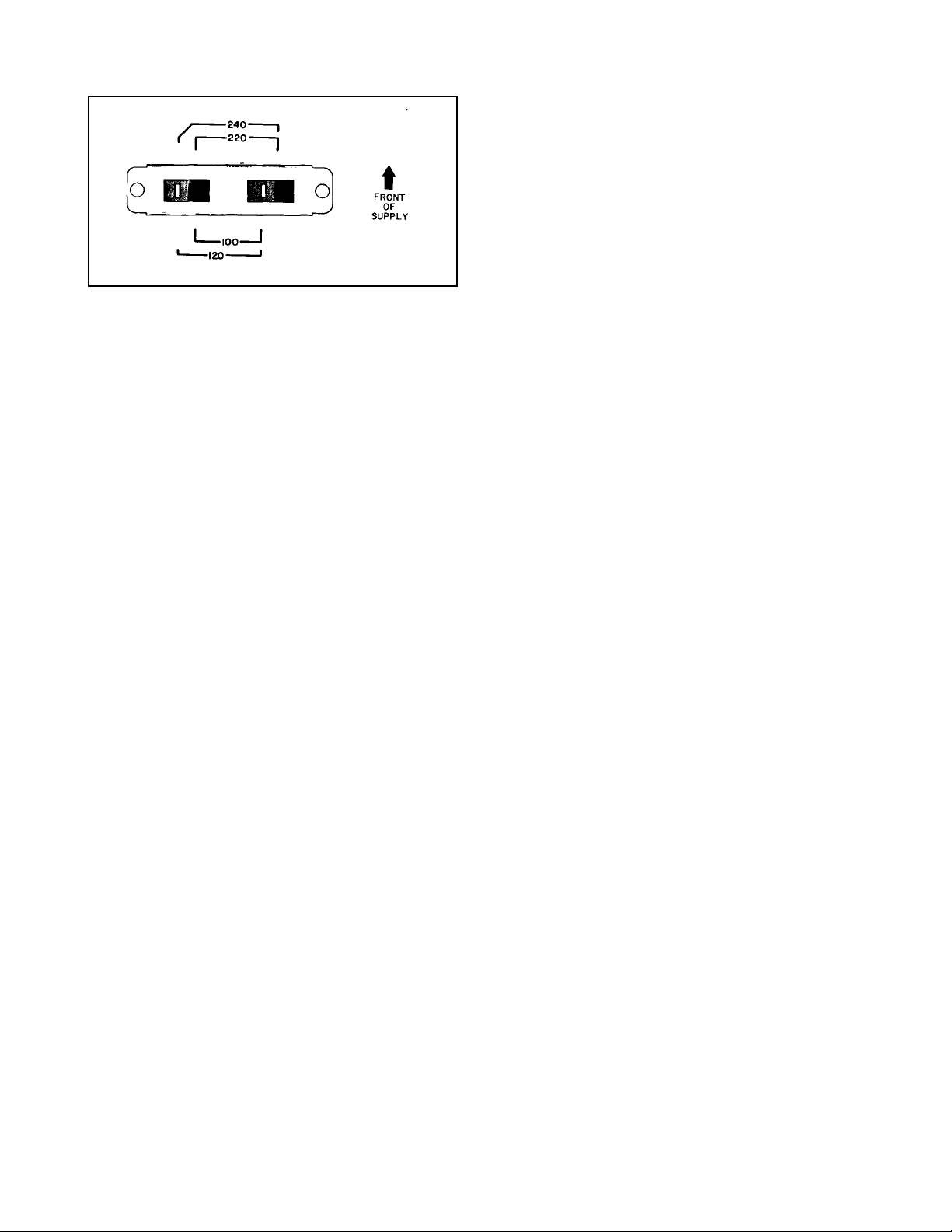
Figure 3-2. line Voltage Selector (Set for 120 Vac)
1. After making certain that the line cord is disconnected from a source of power, remove the top cover from
the supply and set the two sections of the line voltage
selector switch for the desired line voltage (see Figure 3-2).
2. Check the rating of the installed fuse and replace it with the correct value, if necessary. For options 100
or 120, use a normal time-constant 2-amp fuse (HP Part No.
2110-0002). For Options 220 or 240, use a normal timeconstant 1-amp fuse (HP Part No. 2110-0001).
3. Mark the instrument clearly with a tag or label
indicating the correct line voltage to be used.
3-6 OPERATION
3-10 Overload Protection Circuits
3-11 ±20-Volt Current Limit. The +20V and -20V
outputs are individually protected against overload or shortcircuit damage by separate current limit circuits adjusted
at the factory to limit the output current to 0.55A ±5%.
(This is 110% of the maximum rated output.) The current
limits can be set by adjusting resistor R6 for the +20V
output and R26 for the -20V output. (See paragraph 5-47
for current limit calibration instructions.) No deterioration of
supply performance occurs if the output current remains
below the current limit setting. If a single load is
connected between the +20V and -20V outputs, the circuit
set for the lesser current limit will limit the output.
3-12 +6V Current Foldback (Model 6236B). The overload and short-circuit protection circuit for the +6V output
of the Model 6236B reduces the output current limit as the
output terminal voltage decreases. (The operating region of
the +6V output is enclosed by heavy lines in Figure 3-3).
The maximum rated output current is 2.5A and the current
limit is factory-adjusted to operate at 2.75A ±5% when
the output is 6 volts. At lower output voltages, the circuit
reduces the maximum obtainable output current linearly
until 1A ±15% flows when the output is shorted.
The shortcircuit current cannot be adjusted, but R46 can be
set to limit the maximum current at 6V to 2.75A ±5%.
(See paragraph 5-47 for current limit calibration instruction.)
3-7 This power supply can be operated individually
or in parallel with another supply (see paragraph 3-19). All
output terminals are isolated from ground. The ±20V and
+6V or +18V outputs use a single common output
terminal. This common (COM) terminal or anyone of the
other output terminals may be grounded to the chassis at
the front panel ground terminal (
outputs may be left floating. Loads can be connected
separately between each of the 0 to 20V output terminals
and the COM terminal, or between the -20V and the +20V
terminals for a 0 to 40V output.
in Figure 3-1 ), or all
3-8 Tracking Ratio Control
3-9 With the TRACKING RATIO control in the FIXED
position, the voltage of the -20V supply tracks that of the
+20V supply within 1% for convenience in varying the
symmetrical voltages needed by operational amplifiers
and other circuits using balanced positive and negative
inputs. Turn the TRACKING RATIO control counterclockwise out of the FIXED position to set the voltage of the 20V supply lower than that of the +20V supply. The
negative supply can be set from a minimum of less than
0.5 volts to a maximum within 10% of the +20V
supply's output. Once this is done, the ±20V VOLTAGE
control still controls both outputs and maintains a
constant ratio between their voltages.
3-13 +18Volt Current Limit (Model 6237B). The +18volt output of the Model 6237B is protected by a fixed current limit circuit that operates at 1.1 A (110% of its maximum rated output). The circuit is similar to the ones in the
±20-volt supplies. (See paragraph 5-47 for calibration
instructions.)
3-14 Operation Beyond Rated Output
3-15 The supply may be able to provide voltages and
currents greater than its rated maximum outputs if the line
voltage is at or above its nominal value. Operation can extend into the shaded areas on the meter faces without
damage to the supply, but performance cannot be
guaranteed to meet specifications. If the line voltage is
maintained in the upper end of the input voltage range,
however, the supply probably will operate within its
specifications.
3-17 Connect each load to the power supply output
terminals using separate pairs of connecting wires. This
minimizes mutual coupling between loads and takes full
advantage of the low output impedance of the supply.
Load wires must be of adequately heavy gauge to maintain
satisfactory regulation at the load. Make each pair of
connecting wires as short as possible and twist or shield
3-2
Page 9

them to reduce noise pick-up. If shielded wire is used,
connect one end of the shield to the power supply
ground terminal and leave the other end unconnected.
3-18 If load considerations require locating output
power distribution terminals at a distance from the power
supply, then the power supply output terminals should be
connected to the remote distribution terminals by a pair of
twisted or shielded wires and each load should be
connected to the remote distribution terminals separately.
3-19 Parallel Operation
3-20 Two or more power supplies can be connected in
parallel to obtain a total output current greater than that
available from one supply. The total output current is the
sum of the output currents of the individual supplies. The
output voltage controls of one power supply should be set
to the desired output voltage, and the other supply set for
a slightly larger output voltage. The supply set to the
lower output voltage will act as a constant voltage source,
while the supply set to the higher output will act as a
current-limited source, dropping its output voltage until it
equals that of the other supply. The constant voltage
source will deliver only that fraction of its rated output
current necessary to fulfill the total current demand.
3-24 Reverse Current Loading. An active load connected
to the power supply may actually deliver a reverse current to
the supply during a portion of its operating cycle. An external
source cannot be allowed to pump current into the supply
without risking loss of regulation and possible damage to the
output capacitor. To avoid these effects, it is necessary to
preload the supply with a dummy load resistor so that the
power supply delivers current through the entire operating
cycle of the load device.
3-25 Reverse Voltage Protection. Internal diodes connected with reverse polarity across the output terminals
protect the output electrolytic capacitors and the driver
transistors from the effects of a reverse voltage applied
across a supply output. Since series regulator transistors
cannot withstand reverse voltage either, diodes are also
connected across them. When operating supplies in
parallel, these diodes protect an unenergized supply that is
in parallel with an energized supply.
3-21 Special Operating Considerations
3-22 Pulse Loading. The power supply will automatically
cross over from constant-voltage to current-limit operation
in response to an increase in the output current over the
preset limit. Although the preset limit may be set higher
than the average output current, high peak currents as
occur in pulse loading may exceed the preset current limit
and cause crossover to occur and degrade performance.
3-23 Output Capacitance. An internal capacitor across
the output terminals of the power supply helps to supply
high-current pulses of short duration during constant-voltage operation. Any capacitance added externally will improve the pulse current capability, but will decrease the
load protection provided by the current limiting circuit. A
high-current output pulse may damage load components
before the average output current is large enough to cause
the current limiting circuit to operate.
Figure 3-3. Current Limit Characteristics of the 6V Supply
(Model 6236B)
3-3
Page 10

SECTION IV
PRINCIPLES OF OPERATION
4-1 OVERALL DESCRIPTION
4-2 This section presents the principles of operation
of the Models 6236B and 6237B Triple Output Power
Supply. Throughout this section refer to the combined
schematic diagram of Figure 7-1.
NOTE
All information in this section applies to both
models unless otherwise indicated.
4-3 The two primary windings of the power transformer
are connected in one of four different ways by setting the
two slide switches mounted on the circuit board. These
switches select one of the nominal ac input voltages for
which the supply is designed: 100V, 120V, 220V, or 240V.
4-4 The transformer secondaries, together with
rectifiers and capacitor filters, provide raw dc for the three
output regulator circuits and for another regulator that provides reference and bias voltages to the output regulators.
4-5 By comparing its output to a high-stability reference, the 0 to +6-volt regulator (6236B) or 0 to +18volt regulator (6237B) holds its output voltage at the
value determined by a front panel control. Any error in
the actual output as compared to the desired output is
amplified by an operational amplifier and applied as
feedback to control the conduction of a series regulator
transistor. As a result, the voltage across the series
transistor varies so as to hold the output voltage constant
at the desired level. The high gain of the voltage
comparison amplifier and the stability of the reference
voltage ensure that input voltage or load current
variations have little effect on the output voltage.
4-6 The 0 to +6-volt output in the Model 6236B is
protected by a current foldback limiter to minimize
dissipation in the series regulator transistor during
overloads. In a current foldback circuit, the current limit
depends on the output terminal voltage and in this regulator
ranges from 2.75A±5% at 6 volts to 1A±15% with the
output shorted. (An output of 2.75A is 110% of the 2.5A
rated maximum at 6 volts.) The operating region of the
+6-volt regulator output is enclosed by a heavy line in
Figure 3-3. If the operating point reaches the diagonal
current limit line, a decrease in load resistance moves the
operating point down the line, reducing the output voltage
and current. Current foldback is controlled by a second
operational amplifier in the regulator that monitors the dc
output current. This current comparison amplifier takes
control of the output away from the voltage comparison
amplifier when the current reaches the design limit.
Removing the overload restores constant voltage
operation automatically.
4-7 The +20-volt regulator has a fixed current limit at
110% of its 0.5 amp maximum rated output but is
otherwise similar to the +6-volt regulator.
4-8 The 0 to -20-volt regulator is, in turn, similar to the
+20-volt regulator except that it resembles a
complementary mirror image of the latter. The output
voltages of the +20volt and -20-volt supplies are both set
by the same front panel control and track each other within
1% in the fixed tracking ratio mode. Precise tracking of the
two outputs is achieved by controlling the positive output
conventionally and using that output as the reference
voltage for the negative output.
4-9 The 0 to +18-volt regulator in the Model 6237B
is similar to the +20-volt regulator. It has a fixed current
limit at 110% of its 1.0 amp output.
4-10 The reference and bias supply provides reference
and bias voltages for the output regulators.
4-11 The turn-on/turn-off control circuit prevents output
transients when the supply is turned on or off. It does this by
delaying the application of certain bias and reference voltages
at turn-on and removing them shortly after turn-off.
4-12 A three-position meter switch selects which of
the supplies has its output voltage and current indicated
on the front panel meters. The proper range of the dualrange meters is selected automatically
4-13 DETAILED CIRCUIT DESCRIPTION
4-14 0 To +20-Volt Regulator
4-15 Voltage Comparison Amplifier. The voltage comparison amplifier in the +20-volt supply controls the conduction of series regulator transistor Q1 so that the voltages at
the two inputs of the amplifier remain equal. A fixed voltage
divider holds its inverting input (U1-2) at -16mV. Its noninverting input (U1-3) monitors the output voltage in series
4-1
Page 11

with the voltage across R1. Since R2 is connected between
the -6.2V reference supply and a point that feedback action
holds near -16mV, its current remains constant. This
current flows through R1 to produce a voltage drop across
R1 proportional to its resistance setting, thus the output
voltage of the supply is proportional to the resistance
setting of R1. At the output of the voltage comparison
amplifier (U1-1), a positive voltage change corresponds to a
decrease in the conduction of Q1.
and returning control to the voltage comparison amplifier.
4-20 Turn-On/Turn-Off Control. When the power supply
is turned on or off, Q15 in the turn-on control circuit withholds turn-on bias from Q1 while the regulator bias voltages
are too low. This prevents an output voltage transient from
occurring before the amplifiers are properly biased. The
output of the -6.2V reference supply is also temporarily
held at a low voltage by Q14, which conducts to short that
output.
4-16 CR2 and CR3 protect the input of the amplifier
against transient overloads, C2 and R4 speed up loop
response time, and C4 and R12 stabilize the supply's
high frequency characteristics.
4-17 OR-Gate. To permit either the voltage comparison
amplifier or the current comparison amplifier to control the
series regulator transistor, the outputs of both amplifiers
are connected to the base of driver Q2 through an OR-gate
composed of CR5 and CR6. CR5 is normally reverse
biased by a negative output from the current comparison
amplifier, permitting the voltage comparison amplifier to
drive Q2 through CR6. An overload drives the output of
the current comparison amplifier positive, forward biasing
CR5 and reducing the supply output. When the overload is
removed, CR5 is reverse biased again and the voltage comparison amplifier resumes control of the output.
4-18 Driver and Series Regulator. The -12.4V output of
the bias supply provides the turn-on bias for series
regulator transistor Q1. Its complete current path includes
Q15, CR59, R 14, and Q1, and returns to common
through current monitoring resistor R8. (It is because this
bias current flows through R8 that the output ammeter
requires the zero offset bias circuit described in paragraph
4-43.) Through the OR-gate, either the voltage or the
current comparison amplifier controls the conduction of
driver Q2, which regulates the flow of turn-off bias
through Q1's base-emitter circuit. The algebraic sum of the
nearly constant turn-on bias through R14 and the variable
turn-off bias through Q2 controls the conduction of series
regulator transistor Q1.
4-19 Current Limit Circuit. In the +20-volt regulator,
the current comparison amplifier compares the voltage
across current monitoring resistor R8 to the fixed voltage
across part of current limit adjust potentiometer R6. The
current limit adjustment is set so that the input voltage to
the current comparison amplifier is negative in the normal
operating region, but becomes zero when the output
current increases to 0.55 amps. When the amplifier's
input voltage reaches zero, it takes control of the
regulator output voltage and reduces it as necessary to
keep the output current from exceeding 0.55 amps.
When the overload is removed, the output of the current
comparison amplifier goes negative, reverse biasing CR5
4-21 Circuit Protection Components. Diodes CR1, CR7,
and CR9 each protect the +20-volt supply from specific
hazards. Output diode CR1 protects the supply components
if a reverse voltage is applied to the output terminals. A
common way for this to occur is for an unenergized supply
to be connected in series with another that is energized. If
the output voltage is turned down quickly while a large
capacitor is connected across the output, CR7 protects
driver Q2 from excessive dissipation by shunting some of its
base current to common. The series regulator diode, CR9,
protects the series regulator transistor from reverse voltage.
Reverse series regulator voltage could occur if a deenergized
supply were connected in parallel with an energized one.
4-22 0 To -20-Volt Regulator
4-23 Instead of using an NPN driver and a PNP series
regulator in the negative output line as in the +20-volt
regulator, the -20-volt regulator uses a PNP driver and an
NPN series regulator in the positive output line. The -20volt regulator circuit is the complementary equivalent of
the +20-volt circuit in other respects, as well. Their
current limit circuits operate similarly. At the outputs of
the current and voltage comparison amplifiers in the -20volt circuit, a negative voltage change corresponds to a
decrease in series regulator conduction. The turn-on bias
for its series regulator transistor, Q3, is supplied from a
positive voltage source, the +7.5V bias supply, and is
switched on and off by Q13 in the turn-on control circuit.
4-24 The -20-volt supply uses the output of the +20volt supply as its reference voltage. As a result, both
outputs are set by a single front panel control and track
each other with in 1% in the fixed tracking ratio mode.
Two resistors in resistor network Z1 are connected in
series between the +20volt and -20-volt outputs. These
resistors are closely matched in resistance and temperature
coefficient so that the voltage across each is exactly half
of the total. The midpoint of this divider is connected to
the non-inverting input of the -20-volt supply's voltage
comparison amplifier. The amplifier's inverting input is
connected to common through R32 to hold it at zero volts.
The amplifier keeps its differential input voltage at zero by
matching the output voltage of the -20-volt supply to that
of the +20-volt supply.
4-2
Page 12

4-25 In the variable tracking ratio mode, the tracking
ratio control connects a fixed resistor in parallel with
the upper part and a rheostat (the variable tracking ratio
control) in parallel with the lower part of the voltage
divider that forms the -20-volt reference. Turning the
control counter- clockwise reduces the resistance of the
rheostat and lowers the voltage of the negative output.
4-26 0 To +6-Volt Regulator (Model 6236B)
4-27 Except for differing component designations and
values, paragraphs 4-15 through 4-18,4-20, and 4-21,
which describe the voltage comparison amplifier, OR-gate,
driver, series regulator, turn-on control, and circuit
protection components of the +20-volt regulator circuit,
also apply to the +6-volt regulator. The only difference in
circuit operation lies in the control of the current
comparison amplifier, and thus the type of current limit the
supply has.
4-28 Current Foldback Circuit. (For this discussion
refer to the Figure 7-1 schematic and to Figure 4-1.) The
differential input signal to the current comparison amplifier
is the algebraic sum of three circuit voltages:
1.The voltage across R49. E
-305mV.
2. The voltage across the lower part of R46 (see
Figure 4-1). E
is proportional to the regulator
R49
output voltage and equals 440mV when the
supply output is 6 volts.
3. The voltage across current monitoring resistor
R48. E
is proportional to the sum of the
R48
regulator output current and the 0.22A bias
current that flows through R54 and R48.
remains constant at
R49
input (U3-5), which is held at -305mV. The negative amplifier output that results is clamped by CR44 and reverse
biases OR-gate diode CR45, leaving the voltage comparison
amplifier in control of the supply's output. If the load resistance is decreased, the higher output current increases
E
until the algebraic sum of E
R48
R48
and E
makes the
R46
current comparison amplifier's inverting input slightly more
negative than the -305mV potential on its non-inverting input. When this happens, the output of this amplifier goes
positive and forward
biases CR45. Since the current through
CR45 tends to reduce the output of the supply, the output
of the voltage comparison amplifier goes negative in opposition to this change and reverse biases CR46 to leave the
current comparison amplifier in control of the output. Now
that the current comparison amplifier is in control and for as
long as the overload remains, the supply's output voltage
and current vary so as to maintain this amplifier's differential input signal near zero volts. This results in the output
current limit characteristics shown in Figure 3-3.
4-30 If we assume for example that the voltage control
is set for 5 volts and the load resistance is slowly
decreased, the supply goes into current limit at about
2.47 amps. Here is why it occurs at that value. At a 5volt supply output, E
order for the algebraic sum of E
is 5/6 of 440mV, or 367mV. In
R46
R46
and E
to go as far
R48
negative as -305mV and drive the amplifier output
positive, E
must reach -672mV. Once E
R48
R48
reaches
this value, the current comparison amplifier controls the
series regulator transistor so as to prevent E
R48
(and thus
the supply's output current) from increasing further. At
0.25 ohms, R48 develops -672mV at 2.69 amps. Since
0.22 amps of the current through R48 is bias current for
Q7, the nominal current limit corresponding to a 5-volt
output is 2.69 amps minus 0.22 amps, or about 2.47
Figure 4-1. Foldback Current Limit Circuit in 6V Supply
4-29 When the supply's output current is below the current limit that corresponds to its output terminal voltage
(see Figure 3-3), the inverting input (U3-6) of the current
comparison amplifier is more positive than its non-inverting
4-31 If the load resistance continues to decrease, it pulls
the output voltage lower. This reduces E
output voltage E
magnitude to E
becomes zero, leaving E
R46
This -305mV drop across R48 corre-
R49
until at a zero
R46
R48
sponds to a 1.22-amp current through R48 and a 1-amp
shortcircuit current at the output of the supply.
4-32 In the +6-volt regulator, as in the +20-volt
regulator, the turn-on bias current for the series regulator
transistor is switched on and off by Q15 in the turn-on
control circuit to prevent output voltage transients.
4-33 0 To +18-Volt Regulator (Model 6237B)
4-34 Except for differing component designations and
4-3
equal in
Page 13

values, paragraphs 4-15 through 4-21, which describe the
voltage comparison amplifier, OR-gate, driver, series regulator, current limit circuit, turn-on control, and circuit
protection components of the +20-volt regulator circuit,
also apply to the +18-volt regulator. In the +18-volt
regulator, as in the +20-volt regulator, the turn-on bias
current for the series regulator transistor is switched on and
off by Q15 in the turn-on control circuit to prevent output
voltage transients.
4-35 Reference and Bias Supply
4-36 The reference and bias supply powers the
operational amplifiers and provides the bias and reference
voltages used throughout the supply. A shunt zener
regulates its +7.5V output. A series transistor regulates its
-12.4 V output, using 6.2-volt zener VR1 as its voltage
reference. The -12.4V output provides a constant current to
VR1, which is the primary voltage reference for the entire
supply.
4-37 Two equal resistors are connected in series
across the -12.4V output. To regulate this output,
voltage comparison amplifier U4 compares the voltage
across one of these resistors to the -6.2V reference and
controls the conduction of series regulator Q11 through
driver Q12. The voltage drop across Q11 is controlled
by feedback so that the voltages at the two inputs of U4
remain equal. Driver Q12 controls Q11 by shunting part
of the base bias supplied by R68.
4-38 During turn-on, the -6.2V reference supply is
temporarily shorted by Q14 in the turn-on control circuit.
By trying to match this low reference, Q11 is initially turned
off. While Q11 is turned off, R69 bypasses current to the
-12.4 V output until the output reaches -9 volts and the
turn-on control circuit removes the short from the reference
and enables the -12.4-volt regulator to operate normally.
4-39 Turn-On/Turn-Off Control Circuit
4-40 Immediately after the supply is energized and
until the output of the -12.4-volt regulator reaches about
-9 volts, the turn-on control circuit withholds turn-on bias
from series regulator transistors Q1, Q3, and Q7 and holds
the -6.2V reference at a low value. This prevents an output
voltage transient by ensuring that the operational amplifiers
are energized and other essential bias voltages are present
before the series regulator transistors are turned on. The
circuit also prevents an output transient when the supply is
turned off by removing the turn-on bias from the series
regulators and shorting the -6.2V reference supply as the
voltage of the -12.4 V supply falls below -9 volts.
4-41 Q13 switches the bias to the -20-volt regulator
on and off, Q14 switches the short across the -6.2-volt
reference supply, and Q15 switches the bias to the +20volt and +6-volt or +18-volt regulators. Q15 remains
turned off until VR2 conducts at 9 volts to switch it on.
While Q15 is off, it holds Q13 biased off and Q14 on;
when Q15 conducts, it turns Q13 and Q14 off.
4-42 Meter Circuits
4-43 Voltmeter. Two of the resistors in resistor
network Z1 are range resistors for the voltmeter. The
accurate ratio of these resistors permits a single calibration
potentiometer, R58 to adjust both ranges simultaneously.
4-44 Ammeter. The range switch connects the
ammeter across the current monitoring resistor of a supply:
R48 in the +6-volt or +18-volt supply, R8 in the +20-volt
supply, or R28 in the -20-volt supply. Each of these
resistors conducts a constant bias current for its series
regulator transistor in addition to the supply's output
current. If no compensation were used, this additional
current would raise the indicated output by up to 8% of full
scale. The resistor networks connected to each range of the
ammeter selector switch apply a bias to the meter to offset
this error. R59 calibrates all ammeter ranges.
4-4
Page 14

SECTION V
MAINTENANCE
5-1 INTRODUCTION
5-2 Upon receipt of the power supply, the performance
test of paragraph 5-6 can be made. This test is suitable for
incoming inspection. Section III contains a quick but less
comprehensive checkout procedure that can be used in lieu
of the performance test if desired.
5-3 If a fault is detected in the power supply while
making the performance test or during normal operation,
proceed to the troubleshooting procedure in paragraph 5-32.
After troubleshooting and repair, repeat the performance
test to ensure that the fault has been properly corrected and
that no other faults exist. Before performing any maintenance checks, turn on the power supply and allow a half
hour warm-up.
5-4 TEST EQUIPMENT REQUIRED
Table 5-1. Test Equipment Required
REQUIRED RECOMMENDED
TYPE CHARACTERISTICS USE MODEL
5-5 Table 5-1 lists the test equipment required to
perform the various procedures described in this section.
5-6 PERFORMANCE TEST
5-7 The following test can be used as an incoming
inspection check and appropriate portions of the test can
be repeated to check the operation of the instrument after
repairs. If the correct result is not obtained for a particular
check, proceed to the troubleshooting procedures of paragraph 5-32.
———
Before applying power to the supply, make
certain that its line voltage selector switch
(S3) is set for the line voltage to be used. (See
CAUTION notice in paragraph 3-2 for additional information on S3.)
CAUTION
———
Digital Sensitivity: 100mV full scale Measure dc voltages: HP 3490A
Voltmeter (min.). Input impedance: calibration procedures
10 megohms (min.).
Variable Range: 90-130 Vac Vary ac input ----Voltage Equipped with voltmeter
Transformer accurate within 1 volt
Oscilloscope Sensitivity: 100µV/cm. Display transient re- HP 180C with 1821A,
Differential input. sponse and ripple and and 1801A or 1803A
noise waveforms. plug-ins.
Repetitive Rate: 60 Hz, 2µs Measure transient See Figure 5-5.
Load Sw. rise and fall time response.
Resistive Value: See paragraph 5-11. Power supply load James G. Biddle
Loads Tolerance: ±5% resistor (fixed resistor ("Lubri-Tact"
or rheostat). Rheostat)
Current Value: See paragraph 5-13. Measure output current Simpson Portable
Sampling Accuracy: 1% (minimum) Shunt, 06703.
Resistor (Shunt)
5-1
Page 15

5-8 General Measurement Techniques
5-9 Connecting Measuring Devices. To achieve valid
results when measuring the load effect, PARD (ripple and
noise), and transient recovery time of the supply,
measuring devices must be connected as close to the
output terminals as possible. A measurement made across
the load includes the impedance of the leads to the load.
The impedance of the load leads can easily.be several
orders of magnitude greater than the supply impedance
and thus invalidate the measurement. To avoid mutual
coupling effects, each measuring device must be
connected directly to the output terminals by separate
pairs of leads.
5-10 When measurements are made at the front panel
terminals, the monitoring leads must be connected at
point A, as shown in Figure 5-1, and not at point B.
Connecting the measuring device at point B would result
in a measurement that includes the resistance of the leads
between the output terminals and the point of connection.
the sampling resistor by its ohmic value. The total
resistance of the series combination should be equal to
the full load resistance as determined in the preceding
paragraphs. Of course, if the value of the sampling
resistor is very low when compared to the full load
resistance, the value of the sampling resistor may be
ignored. The meter shunt recommended in Table 5-1, for
example, has a resistance of only 1 milliohm and can be
neglected when calculating the load resistance of the
supply.
5-14 Figure 5-2 shows a four terminal meter shunt.
The load current through a shunt must be fed to the
extremes of the wire leading to the resistor while the
sampling connec- tions are made as close as possible to
the resistance portion itself.
Figure 5-1. Front Panel Terminal Connections
5-11 Selecting Load Resistors. Power supply specifica-
tions are checked with a full load resistance connected
across the supply output. The resistance and wattage of
the load resistor, therefore, must permit operation of the
supply at its rated output voltage and current. For example,
a supply rated at 20 volts and 0.5 amperes would require a
load resistance of 40 ohms at the rated output voltage. The
wattage rating of this resistor would have to be at least 10
watts.
5.12 Either a fixed or variable resistor (rheostat) can
be used as the load resistance. Using a rheostat (alone or
in series with a fixed resistor) is often more convenient
than using fixed resistors as loads because the latter
may be more difficult to obtain in the exact resistance
required. A supplier of rheostats appropriate for testing
these supplies is listed in Table 5-1.
5.13 Output Current Measurements. For accurate output current measurements, a current sampling resistor
should be inserted between the load resistor and the
output of the supply. An accurate voltmeter is then
placed across the sampling resistor and the output
current calculated by dividing the voltage across the
Figure 5-2. Current Sampling Resistor Connections
NOTE
All instructions in this section apply to Models
6236B and 6237B unless otherwise indiated.
5-15 Rated Output, Tracking, Meter Accuracy,
and Current Limit
5-16 To check that all supplies will furnish their maximum rated output voltage and current, that the ±20V
outputs track each other, that the front panel meters are
accurate, and that the current limit circuits function,
proceed as follows:
Voltmeter Accuracy
a. With no loads connected: energize the supply, connect a digital voltmeter between the +6V terminal (+18V
in Model 6237B) and common (COM), and set the +6V
(+18V) VOLTAGE control so that the DVM indication is as
near as possible to 6 volts (18 volts).
b. Set the METER switch to the +6V (+18V) range
and check the front panel voltmeter indication. It should be
within 4% of the DVM indication.
c. Set the TRACKING RATIO control to the FIXED
position, and check the +20V and -20V ranges of the
panel voltmeter similarly by connecting the DVM to each of
these outputs in turn, setting the ±20V VOLTAGE control
5-2
Page 16

for a 20V DVM indication, and verifying that the panel
meter is accurate within 4%.
Tracking
d. Connect the DVM to the +20V output, set the ±20V
VOLTAGE control for a DVM indication of 20 volts, and
reconnect the DVM to the -20V output without disturbing
the voltage control. The voltage at the -20V output should
be within 1% of the +20Voutput.
Variable Tracking Ratio
e. Leave the ±20V VOLTAGE control set as in step (d),
and use a DVM to monitor the voltage of the -20V supply
while adjusting the TRACKING RATIO control over its
VARIABLE range. The -20V supply should be capable of
being adjusted from less than 0.5 volts to between 18
and 22 volts. Return the TRACKING RATIO control to the
FIXED position.
NOTE
Leave the TRACKING RATIO control in the
FIXED position throughout the remainder of the
performance test.
Rated Output and Ammeter Accuracy
f. Connect 40Ω 10W load resistors across both of the 20V
outputs of the supply and set the ±20V VOLTAGE control for a
±20V output. (All three supplies must be fully loaded while
checking the rated output voltage and current of each supply.)
g. Connect the test setup shown in Figure 5-3 to the +6V
(or +18V) output. Make the total resistance of RL and the
current sampling resistor 2.4 ohms for the Model 6236B (or
18 ohms for the 6237B) to permit operating the output at full
load. RL should have a power rating of at least 20 watts.
h. Close the switch and set the +6V (+18V) VOLTAGE
control so that the DVM indicates a voltage drop across the
current sampling resistor that corresponds to a current of 2.5
amps (6236B) or 1.0 amp (6237B).
i. Set the METE R switch to the +6V (+18V) range and
verify that the front panel ammeter indication is within 4% of
2.5 amps (6236B) or 1.0 amp (6237B).
j. Connect the DVM directly across the output terminals of
the +6V (+18V) supply, record the DVM reading, and then
open the switch in the 6V (18V) load circuit without disturbing
the supply's output terminals. The DVM indication should not
change by more than 2.6mV (6236B) or 3.8mV (6237B).
k. Check the rated output and ammeter accuracy of the
+20V and -20V supplies similarly by connecting the test setup
of Figure 5-3 to each output in turn. For each 20V supply:
make the total resistance of RL and the current sampling
resistor 40
indication, on the DVM of 0.5A, check that panel meter
ohms, set the ±20V VOLTAGE control for a current
indication is within 4% of 0.5A, connect the DVM to
the fully loaded output terminals, and compare the
output voltage before and after the load circuit is
opened. The voltage should not change by more than
4mV. While checking each supply, the other two must
be fully loaded.
Current Limit
l. Disconnect all loads from the supply.
m. Connect the test setup shown in Figure 5-3 to the
+20 volt output. Substitute a short for RL and leave the
load circuit switch open.
n. Set the voltage of the ±20V supplies to 20-volts.
o. Close the load switch and determine the current
flow through the current sampling resistor (meter shunt)
by measuring its voltage drop with the DVM. The current
should be 0.55A ±5%.
p. Check the current limit of the -20V supply in the
same way. Its short-circuit current should also be 0.55A
±5%.
q. (Model 6237B only). Check the current limit of the
+18V supply similarly by setting its output for 18 volts
and using a DVM to measure the current which flows
through a low- resistance current sampling resistor. The
short-circuit current of the +18V supply should be 1.1 A
±5%.
r. (Steps (r) through (t) apply to the 6236B only.)
Connect the test setup shown in Figure 5-3 to the +6V
output. Close the switch, set the total resistance of RL and
the current sampling resistor to an initial value of 2.4 ohms
or greater, and set the output voltage to 6 volts.
s. Reduce the value of RL gradually while observing the
output current indicated by the DVM. The current should
increase to a maximum of 2.75A ±5% before it begins to
decrease.
t. Connect a short across RL and then recheck the
current
5-17 Load Effect (Load Regulation)
Definition: The change ∆E
output voltage resulting from a change in load
resistance from open circuit to the value that yields
maximum rated output current (or vice versa).
5-18 To check the load effect:
a. Connect a full load resistance and a digital voltmeter
across the output of the +20V supply.
b. Turn on the supply and adjust its voltage to its
maximum rated value.
c. Record the voltage indicated on the DVM.
d. Disconnect the load resistance and recheck the DVM
indication. It should be within .01% plus 2mV of the reading in step (c).
e. Repeat steps (a) through (d) for each of the remaining supply outputs.
in the static value of dc
OUT
5-3
Page 17

Figure 5-3. Output Current, Test Setup
5-19 Source Effect (Line Regulation)
Definition: The change,
value of dc output voltage resulting from a change in ac
input voltage over the specified range from low line
(typically 104 Vac) to high line (typically 127 Vac), or
from high line to low line.
5-20 To test the source effect:
a. Connect a variable autotransformer between the in
put power source and the power supply line plug.
b. Connect a full load resistance and a digital voltmeter
across the output of the +20V supply.
c. Adjust the autotransformer for a low line input.
d. Turn on the power, adjust the output of the supply
to its maximum rated voltage, and record the DVM indication.
e. Adjust the autotransformer for a high line input and
recheck the DVM indication. It should be within .01% plus
2mV of the reading in step (d).
f. Repeat steps (b) through (e) for each of the
remaining supply outputs.
∆
E
in the static
OUT
The magnitude of this remaining signal can easily be much
greater than the true ripple developed between the plus
and minus output terminals of the power supply and can
completely invalidate the measurement.
5-23 The same ground current and pickup problems can
exist if an rms voltmeter is substituted in place of the oscilloscope in Figure 5-4. However, the oscilloscope display,
unlike the true rms meter reading, tells the observer immediately whether the fundamental period of the signal displayed is 8.3 milliseconds (1/120 Hz) or 16.7 milliseconds
(1/60 Hz). Since the fundamental ripple frequency present
on the output of an HP supply is 120 Hz (due to full-wave
rectification). an oscilloscope display showing a 120 Hz
fundamental component is indicative of a "clean" measurement setup, while the presence of a 60 Hz fundamental
usually means that an improved setup will result in a more
accurate (and lower) value of measured ripple.
5-21 PARD (Ripple and Noise)
superimposed on the dc output of a regulated power
supply. Ripple and noise may be specified and measured
in terms of its rms or peak-to-peak value.
5-22 Measurement Techniques. Figure 5-4A shows an
incorrect method of measuring p-p ripple. Note that a continuous ground loop exists from the third wire of the input
power cord of the supply to the third wire of the input
power cord of the oscilloscope via the grounded power
supply case, the wire between the negative output
terminal of the power supply and the vertical input of the
scope, and the grounded scope case. Any ground current
circulating in this loop as a result of the difference in
potential E
drop that is in series with the scope input. This IR drop,
normally having a 60 Hz line frequency fundamental, plus
any pickup on the unshielded leads interconnecting the
power supply and scope, appears on the face of the CRT.
Definition: The residual ac voltage that is
G
between the two ground points causes an IR
Figure 5-4. Ripple and Noise, Test Setup
5-4
Page 18

5-24 Figure 5-4B shows a correct method of measuring
g
p
the output ripple of a constant voltage power supply
using a single-ended scope. The ground loop path is
broken by floating the power supply output. To ensure
that no potential difference exists between the supply
and the oscilloscope, it is recommended that they both
be plugged into the same ac power bus. If the same bus
cannot be used, both ac grounds must be at earth
ground potential.
5-25 Either a twisted pair or, preferably, a shielded twowire cable should be used to connect the output terminals
of the power supply to the vertical input terminals of the
scope. When using a twisted pair, care must be taken that
one of the two wires is connected to the grounded input
terminal of the oscilloscope to ensure that the supply
output is safely grounded. When using shielded two-wire, it
is essential for the shield to be connected to ground at one
end only to prevent ground current flowing through this
shield from inducing a signal in the shielded leads.
5-26 To verify that the oscilloscope is not displaying
ripple that is induced in the leads or picked up from the
grounds, the (+) scope lead should be shorted to the (-)
scope lead at the power supply terminals. The ripple value
obtained when the leads are shorted should be subtracted
from the actual ripple measurement.
5-27 In most cases, the single-ended scope method of
Figure 5-4B will be adequate to eliminate extraneous ripple
so that a satisfactory measurement may be obtained.
However, in more stubborn cases (or if high frequency
noise up to 20 MHz must be measured). it may be
necessary to use a differential scope with floating input as
shown in Figure 5-4C. If desired, two single-conductor
shielded cables may be substituted in place of the shielded
two-wire cable with equal success. Because of its common
mode rejection. a differential oscilloscope displays only the
difference in signal between its two vertical input terminals,
thus ignoring the effects of any common mode signal pro-
duced by the difference in the ac potential between the
power supply case and scope case. Before using a differen-
tial input scope in this manner, however, it is imperative
that the common mode rejection capability of the scope be
verified by shorting together its two input leads at the
power supply and observing the trace on the CRT. If this
trace is a straight line, then the scope is properly ignoring
any common mode signal present. If this trace is not a
straight line, then the scope is not rejecting the ground
signal and must be realigned in accordance with the manu-
facturer's instructions until proper common mode rejection
is attained
an oscilloscope with sufficient bandwidth (20 MHz) must
be used. Ripple and noise measurements can be made at
any input ac line voltage combined with any dc output
voltage and load current within rating.
a. Connect an oscilloscope or rms voltmeter across an
output of the supply as shown in Figures 5-4B or 5-4C.
b. Energize the supply and observe the oscilloscope or
meter indication. The ripple and noise should not be
greater than 0.35mV rms or 1.5mV peak-to-peak.
c. Repeat for the remaining supply outputs.
5-29 Load Transient Recovery Time
Definition: The time "X" for output voltage
recovery to within "Y" millivolts of the nominal output
voltage following a "Z" amp step change in load current,
where: "Y" equals 15mV, and "Z" is the specified load
current change, equal to half of the current rating of the
supply. The nominal output voltage is defined as the dc
level halfway between the static output voltage before
and after the imposed load change.
5-30 Measurement Techniques. Care must be taken in
switching the load resistance on and off. A hand-operated
switch in series with the load is not adequate since the resulting one-shot displays are difficult to observe on most
oscilloscopes and the arc energy occurring during switching
completely masks the display with a noise burst.
load switching devices are expensive if reasonably rapid load
Transistor
5-28 Measurement Procedure. To measure the ripple
and noise on each supply output, follow the steps
below, If a high frequency noise measurement is desired,
5-5
ure 5-5. Load Transient Recovery Time, Test Setu
Fi
Page 19

current changes are to be achieved. Instead, a mercury-
—
wetted relay should be used for loading and unloading the
supply. Connect it in the load switching circuit shown in
Figure 5-5. When this load switch is connected to a 60 Hz
ac input, the mercury-wetted relay will open and close 60
times per second. The 25K control adjusts the duty cycle
of the load current switching to reduce jitter in the oscilloscope display. This relay may also be used with a 50 Hz ac
input.
5-31 Measurement Procedure. To measure the load
transient recovery time, follow the steps below for each
supply output. Transient recovery time may be measured at
any input line voltage and any output voltage within rating.
For this supply the specified load change is between half load
and full load.
a. Connect the test setup shown in Figure 5-5. Both
load resistors (RL) are twice the normal value of a full load
resistance.
b. Turn on the supply and close the line switch on the
repetitive load switch.
c. Set the oscilloscope for internal sync and lock on
either the positive or negative load transient spike.
d. Set the vertical input of the oscilloscope for ac coupling so that small dc level changes in the output voltage of
the power supply will not cause the display to shift.
e. Adjust the horizontal positioning control so that the
trace starts at a point coincident with a major graticule
division. This point then represents time zero.
f. Adjust the vertical centering of the scope so that the
tail ends of the no-load and full-load waveforms are
symmetrically displaced about the horizontal center line of
the oscilloscope. This center line now represents the nominal
output voltage defined in the specification.
g. Increase the sweep rate so that a single transient
spike can be examined in detail.
h. Adjust the sync controls separately for the positive
and negative going transients so that not only the recovery
waveshape but also as much as possible of the rise time of
the transient is displayed.
i. Starting from the major graticule division
representing time zero, count to the right 50µs and
vertically 15mV. Recovery should be within these
tolerances, as illustrated in Figure 5-6.
5-32
5-33 Before attempting to troubleshoot this instrument,
ensure that the fault is in the instrument itself and not in
an associated piece of equipment. You can determine this
without removing the covers from the instrument by using
the appropriate portions of the performance test of
paragraph 5-6.
5-34 A good understanding of the principles of operation is a helpful aid in troubleshooting, and the reader is
advised to review Section IV of the manual before beginning detailed troubleshooting. Once the principles of operation are understood, proceed to the initial troubleshooting
procedures in paragraph 5-35.
5-35
5-36 If a malfunction is found, follow the steps below:
a. Disconnect input power from the supply and
remove all loads from the output.
b. Table 5-2 lists the symptoms and probable
causes of several possible troubles. If the symptom is one
of those listed, make the recommended checks.
proceed to Table 5-3. This table provides an initial
troubleshooting procedure that also directs you to the
more detailed procedures which follow it.
TROUBLESHOOTING
CAUTION
——
Before applying power to the supply, make
certain that its line voltage selector switch (S3)
is set for the line voltage to be used. (See
CAUTION notice in paragraph 3-2 for additional
information on S3.
)
———
Initial Troubleshooting Procedure
c. If none of the symptoms of Table 5-2 apply,
Figure 5-6. Load Transient Recovery Time Waveforms
5-37 The numbered test points referred to in the troubleshooting procedures are identified on the circuit schematic
and on the component location diagram at the rear of the
manual.
5-38 Open Fuse Troubleshooting
5-39
5-6
Although transients or fatigue can cause a fuse to
Page 20

Table 5-2. Miscellaneous Troubles
SYMPTOM CHECK - PROBABLE CAUSE
High ripple a. Check operating setup for ground loops (see paragraph 5-22).
b. Check main rectifiers (CR11, CR12, CR31, CR32, CR51, CR52)
for open.
c. Supply may be operating in current limit mode. Check current
limit adjustment, paragraph 5-26, steps (l) thru (t).
Will not current limit Check for open OR-gate diodes (CR5, CR25, CR45) or defective
current limit amplifier (U1, U2, U3).
Poor load or line regulation a. Check bias and reference voltages, Table 5-4.
Oscillation or poor transient a. High frequency oscillations (above 50 kHz) can be caused by an
recovery time open C4, C14, or C24.
Transient voltage overshoot a. Overshoot only in the -20V supply can be caused by a
at turn-on or turn-off. shorted Q13.
STEP ACTION RESPONSE NEXT ACTION
1 Check output voltage of +20V a. Normal a. Proceed to step (2).
supply.
b. Check main rectifiers and filters for opens.
b. A defective output capacitor (C1, C11, or C21) can cause
oscillations in one of many frequency ranges.
c. Oscillation only in the current limiting mode can be caused
by an open C3, C13, or C23.
b. Overshoot in all three supply outputs can be caused by an
open Q14 or a shorted Q15.
Table 5-3. Initial Troubleshooting Procedure
b. Zero volts b. Check ac line fuse (F1). If blown, proceed
to paragraph 5-38. If not blown, check
bias and reference voltages (Table 5-4).
c. Output voltage lower c. Check bias and reference voltages
or higher than rating. (Table 5-4).
2 Check output voltage of -20V a. Normal a. If +20V and -20V outputs are both
supply in fixed tracking ratio normal with no load, a supply might
mode. be current limiting under load. To check
this adjustment see paragraph 5-16,
steps (l) thru (p).
b. High, low, or zero b. Proceed to -20V supply troubleshooting,
output voltage. Table 5-6.
5-7
Page 21

Table 5-3. Initial Troubleshooting Procedure (Continued)
STEP ACTION RESPONSE NEXT ACTION
3 Check output of +6V supply a. Normal a. If the output of this supply is normal
(Model 6236B) unloaded but its voltage falls when
or+18V supply loaded, check the current limit adjust
(Model 6237B). ment, paragraph 5-16, steps (q) thru (t).
b. High, low, or zero b. Proceed to Table 5-7.
output voltage.
Table 5-4. Bias and Reference Voltage Check
STEP ACTION RESPONSE PROBABLE CAUSE
1 Check +7.5V bias, TP1 to a. Normal a. Proceed to step (2).
common (+7.5V±5%)
b. Voltage high b. Check VR3 for open.
c. Voltage low c. Check VR3 for short.
Note: A short within U1, U2, U3, or U4 can
cause low +7.5V or -12.4V bias voltages
2 Check -6.2V reference, a. Normal a. Proceed to step (3).
TP2 to common (-6.2V±5%)
b. Voltage high b. Check VR1 for open.
c. Voltage low c. Check VR1 and Q14 for short, VR2
and Q15 for open. (A short within U4
could reduce this voltage.)
3 Check -12.4V bias, a. Normal a. Proceed to +20V supply troubleshooting
TP3 to common (-12.4V±5%) Table 5-5.
b. High voltage b. Check Q11 for short, Q12 for open,
and Z1 for open between pins 3 and 5.
c. Low voltage c. Check Q11 for open, Q12 for short, and
Z1 for open between pins 1 and 3.
5-8
Page 22

Table 5-5. +20V Supply Troubleshooting
SYMPTOM STEP - ACTION RESPONSE - PROBABLE CAUSE
High output voltage 1. Attempt to turn down a. If output voltage remains high, check Q1, Q15,
(higher than rating) loop by shorting Q15 emitter- and CR9 for short.
to-base
b. If output voltage falls to near zero, remove short
from Q15 and proceed to step (2).
2. Measure voltage at Out- a. If TP4 is approx. -0.7V, check for open CR6 or
put of OR-gate (TP4). R1, and defective U1.
b. If TP4 is approx. +0.7V, check for defective Q2.
Low output voltage 1. Measure voltage at out- a. If TP4 is between zero and -0.7V, check for
(lower than rating) put of OR-gate (TP4). open Q1, Q15, R14, or CR59, and defective Q2.
b. If TP4 is approx. +0.7V, proceed to step (2).
2. Measure voltage at TP8. a. If voltage at TP8 is positive, check Z1 for open
between pins 5 and 13, check R8 for open, and
check for defective R6 or U1.
b. If TP8 is approx. -0.7V, proceed to step (3).
3. Measure voltage at TP7. a. If TP7 is approx. +0.7V, check CR6 for short.
b. If TP7 is approx. +1.4V, proceed to step (4).
4. Measure voltage at TP13. a. If TP13 is approx. -0.7V, replace U1.
b. If TP13 is zero volts, check for open R10, and
shorted CR2 or CR3.
c. If TP13 is approx. +0.7V, check for open R2,
shorted R1, or leaky or shorted C2.
Table 6-6. -20V Supply Troubleshooting
SYMPTOM STEP - ACTION RESPONSE - PROBABLE CAUSE
The +20V supply must operate properly
NOTE:
before troubleshooting the -20V supply.
High output voltage 1. Attempt to turn down a. If output voltage remains high, check Q3, CR29,
(more than 1% greater loop by shorting Q13 and Q13 for short.
than +20V supply in emitter-to-base. b. If output falls to near zero, remove short from Q13 and
fixed tracking ratio proceed to step (2).
mode). 2. Measure voltage at out
put of OR-gate (TP5) a. If voltage at TP5 is zero or negative, check for
defective Q4.
5-9
b. If TP5 is positive, proceed to step (3)
Page 23

Table 5-6. -20V Supply Troubleshooting (Continued)
SYMPTOM STEP - ACTION RESPONSE - PROBABLE CAUSE
3. Measure voltage at TP14. a. If TP14 is approx. -0.7V, check for open CR26
or defective U2.
b. If TP14 is approx. +0.7V, check Z1 for open from
pin 7 to 12 or for short from pin 6 to 12.
Low output voltage 1. Measure voltage at TP5. a. If voltage at TP5 is zero or positive, check for open
(more than 1% lower Q3, Q13, or R34, and defective Q4.
than +20V supply in
fixed tracking ratio b. If TP5 voltage is approx. -0.7V, proceed to step
model (2).
2. Measure voltage at TP9. a. If TP9 is negative, check for open Z1 between
pins 5 and 15, open R28, and defective R26 or U2.
b. If TP9 is approx. +0.7V, proceed to step (3).
3. Measure voltage at TP10. a. If TP10 is approx. -0.7V, check CR26 for short.
b. If TP10 is -1.0 to -1.4V, proceed to step (4).
4. Measure voltage at TP14. a. If TP14 is approx. +0.7V, replace U2.
b. If TP14 is zero volts, check for shorted CR22 or CR23.
c. If TP14 is approx. -0.7V, check 2;1 for open between
pins 6 and 12 or short between pins 7 and 12, and
check for leaky or shorted C12.
Table 5-7. +6V or +18V Supply Troubleshooting
SYMPTOM STEP – ACTION RESPONSE - PROBABLE CAUSE
High output voltage 1. Attempt to turn down loop a. If output voltage remains high, check Q7, Q15,
(higher than rating) by shorting Q15 emitter-to-base. and CR49 for short.
b. If output voltage falls to near zero, remove short
from Q15 and proceed to step (2).
2. Measure voltage at output a. If TP6 is approx. -0.7V, check for open CR46 or
of OR-gate (TP6). R41, and defective U3.
b. If TP6 is approx. +0.7V, check for defective Q8.
Low output voltage 1. Measure voltage at output a. If TP6 is between zero and -0.7V, check for open
(lower than rating) of OR-gate (TP6) Q7, Q15, R54, or CR59, and defective Q8.
b. If TP6 is approx.+0.7V, proceed to step (2).
5-10
Page 24

Table 5-7. +6V or +18V Supply Troubleshooting (Continued)
SYMPTOM STEP - ACTION RESPONSE - PROBABLE CAUSE
2. Measure voltage at TP12. a. If voltage at TP12 is positive, check for shorted
R49, open R48, open Z1 between pins 5 and 14,
and defective R46 or U3.
b. If TP12 is approx. -0.7V, proceed to step (3).
3. Measure voltage at TP11.
a. If TP11 is approx. +0.7V, check CR46 for short.
b. If TP11 is approx. +1.4V, proceed to step (4).
4. Measure voltage at TP15.
open R42, or leaky or shorted C22.
blow, it is a good idea to inspect the unit for obvious
shorts such as damaged wiring, charred components, or
extraneous metal parts or wire clippings in contact with
circuit board conductors before replacing the fuse. The
rating of the correct replacement fuse depends on the line
voltage option of the instrument: for Options 100 or 120,
use a normal time-constant 2-amp fuse (HP Part No. 2110-
0002); for Options 220 or 240, use a normal timeconstant 1-amp fuse (HP Part No. 2110-0001).
5-40 REPAIR AND REPLACEMENT
5-41 Series Regulator Replacement
5-42 To remove and replace a series regulator transistor:
a. Remove the top and bottom covers from the instru-
ment.
b. Remove the collector screws and unsolder the base
and emitter leads from the board to remove the transistor.
c. To replace the transistor, follow the below reassembly
order, as viewed from the bottom of the heat sink: collector
screws, P. C. board, heat sink, two insulating bushings (in
collector screw holes in heatsink), silicon grease (Dow DC-5
or HP 8500-0059), mica insulator, another coating of silicon
grease, transistor, lock-washers, and hex-nuts.
d. Resolder the emitter and base pins to the circuit
board.
5-43 Semiconductor Replacement
5-44 Table 6-4 contains replacement data for the
semiconductors used in this power supply. When replacing
a. If TP15 is approx. -0.7V, replace U3.
b. If TP15 is zero volts, check for open R50, and
shorted CR42 or CR43.
c. If TP15 is approx. +0.7V, check for shorted R41,
a semiconductor, use the listed Hewlett-Packard part or
exact commercial replacement if these are available. If
neither of these are immediately available and a part is
needed without delay for operation or troubleshooting
verification, the parts designated Note 1, Alternate Part
Number can be tried with a high probability of success.
5-45 Notice that both the commercial and alternate replacements listed in Table 6-4 apply only to the HP power
supplies covered by this manual and their use in any other
Hewlett-Packard instrument is not necessarily
recommended because of inclusion in this table.
5-46 ADJUSTMENT AND CALIBRATION
5-47 Current Limit Adjustment
5-48 ±20V Supplies. Perform the following steps to
adjust the current limit circuit in the +20V or -20V supply.
Potentiometer R6 sets the +20V and R26 the -20V current
limit.
a. Turn the TRACKING RATIO control to the FIXED
position.
b. Turn the current limit adjustment pot (R6 or R26)
fully counterclockwise to its minimum setting.
c. Connect the test circuit of Figure 5-3 to the output of
the supply to be adjusted. Use a 40Ω 10W resistor for RL.
d. Turn on the supply and set the ±20V VOLTAGE
control for maximum output (fully clockwise).
e. Turn the current limit pot (R6 or R26) slowly
clockwise until the DVM indicates a voltage drop across the
shunt corresponding to a current of 0.55A ±5%.
5-11
Page 25

5-49 +6V Supply (Model 6236B). To adjust the
current limit circuit in the +6V supply, proceed as follows;
a. Check the setting of the current limit by performing
steps (r) and (s) of paragraph 5-16. (Be sure to set the
output voltage to 6 volts.) If reducing the load resistance
permits the current to exceed 2.9A, stop, turn R46 slightly
clockwise, and repeat the test. If, instead, the current
begins to fall before it reaches 2.6A, turn R46 slightly
counterclockwise and repeat the test.
b. Recheck the setting and readjust R46 until the test
shows that the current limit circuit begins to reduce the
current when a decreasing load resistance increases it to
2.75A ±5%.
5-50 +18V Supply (Model 6237B). To adjust the
current limit circuit in the +18V supply, proceed as follows:
a. Turn current limit adjustment pot (R46) fully clock
wise to its minimum setting.
b. Connect the test circuit of Figure 5-3 to the output
of the +18V supply. Use an 18Ω 20W resistor for RL.
c. Turn on the supply and set the +18V VOLTAGE
control for maximum output (fully clockwise).
d. Turn current limit pot (R46) slowly counterclockwise
until the DVM indicates a voltage drop across the shunt
corresponding to a current of 1.1 A ±5%.
5-51 Meter Calibration
5-52 Panel Voltmeters. Check the accuracy of the
panel voltmeter by performing steps (a), (b), and (c) of the
procedure in paragraph 5-16. Since the same range
resistors are used in both 20-volt ranges, their accuracy
will be the same. Adjust R58 so that the percentage error
in the +6V range (or +18V range) is equal to the error in
the 20-volt ranges. Turn R58 clockwise to increase the
indications or counterclockwise to decrease them. If R58
cannot calibrate all voltmeter ranges to within the ±4%
specification, check the values of the resistors in the
voltmeter circuit.
5-53 Panel Ammeter. Check and calibrate the panel
ammeter by following the steps below.
a. Connect the test setup shown in Figure 5-3 to the
+6V (or +18V) output. Make the total resistance of R
and the
or 18 ohms (6237B) to permit operating the supply at its
full rated output. RL should have a power rating of at least
20 watts.
control so that the DVM indicates an output of 2.5A
(6236B) or 1.0A (6237B).
+6V or +18V range.
using the same test setup but making RL a 40Ω 10W
resistor and setting the voltage control for a 0.5A output
current. Record the panel ammeter accuracy on each 20-volt
range.
three ranges or counterclockwise to decrease them.
within the ±4% specification, check the values of the resistors in the circuit, including current monitoring resistors R8,
R28, and R48.
current sampling resistor 2.4 ohms (Model 6236B)
b. Close the switch and set the +6V (+18V) VOLTAGE
c. Check and record the panel ammeter accuracy on the
d. Check each of the 20-volt ammeter ranges similarly,
e. Turn R59 clockwise to increase the indications on all
f. If R59 cannot calibrate all three ammeter ranges to
L
5-12
Page 26

SECTION VI
REPLACEABLE PARTS
6-1
6-2 This section contains information for ordering replacement parts. Table 6-4 lists parts in alpha-numeric
order by reference designators and provides the following
information:
the part number is listed except in instruments containing
many sub-modular assemblies, in which case the TQ appears
the first time the part number is listed in each assembly.
Refer to Table 6-3 for manufacturer's name and address.
complete maintenance of one instrument during one year of
isolated service.
listed at the end of Table 6-4 under Mechanical and /or
Miscellaneous. The former consists of parts belonging to and
grouped by individual assemblies; the latter consists of all
parts not immediately associated with an assembly.
6-3
6-4 To order a replacement part, address order or inquiry to your local Hewlett-Packard sales office (see lists
at rear of this manual for addresses). Specify the
following information for each part: Model, complete serial
number, and any Option or special modification (J)
numbers of the instrument; Hewlett-Packard part number;
circuit reference designator; and description. To order a
part not listed in Table 6-4, give a complete description of
the part, its function, and its location.
INTRODUCTION
a. Reference Designators. Refer to Table 6-1.
b. Description. Refer to Table 6-2 for abreviations.
c. Total Quantity (TQ). Given only the first time
d. Manufacturer's Part Number or Type.
e. Manufacturer's Federal Supply Code Number.
f. Hewlett-Packard Part Number.
g. Recommended Spare Parts Quantity (RS) for
h. Parts not identified by a reference designator are
ORDERING INFORMATION
Table 6-1. Reference Designators
A = assembly E = miscellaneous
B = blower (fan) electronic part
C = capacitor F = fuse
CB = circuit breaker J = jack, jumper
CR = diode K = relay
DS = device, signaling L = inductor
(lamp) M = meter
Table 6-1. Reference Designators (Continued)
P = plug V = vacuum tube,
Q = transistor neon bulb,
R = resistor photocell, etc.
S = switch VR = zener diode
T = transformer X = socket.
TB = terminal block Z = integrated cir TS = thermal switch cuit or network
Table 6-2. Description Abbreviations
A = ampere mod. = modular or
Ac = alternating current modified
assy. = assembly mtg = mounting
bd = board n = nano = 10
bkt = bracket NC = normally closed
°C = degree Centigrade NO = normally open
cd = card NP = nickel-plated
coef = coefficient Ω = ohm
comp = composition obd = order by
CRT = cathode-ray tube description
CT = center-tapped OD = outside diameter
dc = direct current p = pico=10
DPDT = double pole, P.C. = printed circuit
double throw pot. = potentiometer
DPST = double pole, p-p = peak-to-peak
single throw ppm = parts per million
elect = electrolytic pvr = peak reverse
encap = encapsulated voltage
F = farad rect = rectifier
°F = degree Farenheit rms = root mean square
fxd = fixed Si = silicon
Ge = germanium SPDT = single pole,
H = Henry double throw
Hz = Hertz SPST = single pole,
IC = integrated circuit single throw
ID = inside diameter SS = small signal
incnd = incandescent T = slow-blow
k = kilo = 103 tan. = tantalum
m = milli = 10
M= mega = 106V= volt
µ= micro = 10-6var = variable
met. = metal ww = wirewound
mfr = manufacturer W = Watt
-3
Ti = titanium
-9
12
6-1
Page 27

Table 6-3. Code List of Manufacturers
CODE MANUFACTURER ADDRESS
01121 Allen Bradley Co. Milwaukee, WI
02114 Ferroxcube Corp. Saugerties, NY
02582 Clarostat Mfg. Co., Inc. Dover, NH
02735 Radio Corp. of America, Solid State and
Receiving Tube Div. Somerville, NJ
03508 G. E. Semiconductor
Products Dept. Syracuse, NY
04200 Sprague Electric Co. North Adams, MA
04713 Motorola Semiconductor
Prod. Inc. Phoenix, AZ
05524 Dale Electronics Inc. Columbus, NE
05820 Wakefield Engr. Inc. Wakefield, MA
05917 Aktiebolaget Rifa Bromma, Sweden
07716 IRC Div. of TRW Inc. Burlington, IA
CODE MANUFACTURER ADDRESS
09353 C & K Components Inc. Newton, MA
19701 Electra/Midland Corp. Mineral Wells, TX
27014 National Semiconductor
Corp. Santa Clara, CA
28480 Hewlett-Packard Co. Palo Alto, CA
61637 Union Carbide Corp. New York, NY
71450 CTS Corp. Elkhart, IN
72136 Electro Motive Mfg.Co., Inc.
Willimantic, CT
75042 IRC Div. of TRW, Inc. Philadelphia, PA
75915 Littlefuse,Inc. DesPlaines,IL
6-2
Page 28

Table 6-4. Replaceable Parts
REF. MFR. MFR. HP
DESIG. DESCRIPTION TQ* PART NO. CODE PART NO. RS
Printed Circuit Board Assy.
C1 fxd, elect 180µF 50V 2/3 672D047 04200 0180-0634 1
C2 fxd, tant 6.8µF 35V 3 150D685X9035B2 04200 0180-0116 1
C3, 4 fxd, polyester 2200pF 200V 2 292P22292-PTS 04200 0160-0154 1
C7 fxd, elect 1450µF 45V 2 (Type68D) D39532 04200 0180-1893 1
C8, 9 fxd, cer .05µF 400V 6/4 33C17A3-CDH 04200 0150-0052 1
C11 fxd, elect 180µF 50V 672D047 04200 0180-0634
C12 fxd, tant 6.8µF 35V 150D685X9035B2 04200 0180-0116
C13 fxd, polyester .01µF 200V 2 292P10392-PTS 04200 0160-0161 1
C14 fxd, polyester 3300pF 200V 1 292P33292-PTS 04200 0160-0155 1
C17 fxd, elect 1450µF 45V (Type 68D) D39532 04200 0180-1893
C18, 19 fxd, cer .05µF 400V 33C17A3-CDH 04200 0150-0052
C21
6236B fxd, elect 1000µF 12V 1 627D046 04200 0180-0633 1
6237B fxd, elect 180µF 50V 672D047 04200 0180-0634
C22 fxd, tant 6.8µF 35V 150D685X9035B2 04200 0180-0116
C23 fxd, cer .005µF 100V 1 C023B101E502MS27 04200 0160-2639 1
C24 fxd, polyester .01µF 200V 292P10392-PTS 04200 0160-0161
C27
6236B fxd, elect 5600µF 25V 1 (Type 32D) D40018 04200 0180-1921 1
6237B fxd, elect 3000µF 40V 1 32D5278-DQB 04200 0180-1899 1
C28, 29
6236B fxd, cer .05µF 400V 33C17A3-CDH 04200 0150-0052
6237B Not used
C30
6236B Not used
6237B fxd, cer 0.1µF 500V 1 41C92B5-CDH 04200 0160-0269 1
C31
6236B fxd, tant 0.47µF 35V 1 150D474X9035A2 04200 0180-0376 1
6237B fxd, elect 0.15µF 35V 1 T110A154K035AS 61637 0180-0218 1
C32 fxd, mica 330pF 500V 1 obd 72136 0160-2012 1
C33 fxd, elect 490µF 85V 1 (Type 68D) D38618 04200 0180-1888 1
C34 fxd, paper 0.1µF 250Vac 1 PME271-M-610 05917 0160-4065 1
CR1 Diode, Si 1A 200V 13/15 1N5059 1901-0327 7
CR2-7 Diode, Si 17 1N485B 1901-0033 7
CR9, 11, 12, 21 Diode, Si 1A 200V 1N5059 1901-0327
CR22-26 Diode, Si 1N485B 1901-0033
CR28,29,31,32 Diode, Si 1A 200V 1N5059 1901-0327
CR41 Diode, Si 1.5A 200V 3 1N4999 1901-0416 3
CR42, 43 Diode, Si 1N485B 1901-0033
CR44 Diode, stabistor 150mA 15V 2 STB523 03508 1901-0460 2
CR45-47 Diode, Si 1N485B 1901-0033
CR49 Diode, Si 1A 200V 1N5059 1901-0327
CR51, 52 Diode, Si 1.5A 200V 1N4999 1901-0416
CR53, 54
6236B Not used
6237B Diode, Si 1A 200V 1N5059 1901-0327
CR55, 56 Diode, Si 1A 200V 1N5059 1901-0327
CR57 Diode, stabistor 150mA 15V STB523 03508 1901-0460
CR59 Diode, Si 1A 200V 1N5059 1901-0327
* 6236B/6237B
6-3
Page 29

Table 6-4. Replaceable Parts (Continued)
REF. MFR. MFR. HP
DESIG. DESCRIPTION TQ* PART NO. CODE PART NO. RS
CR60 Diode, Si 1N485B 1901-0033
L1, 2, 3 Inductor, ferrite bead 3 56-590-65/4A6 02114 9170-0894 1
(Q2, Q3, CR49)
Q2 SS NPN Si 3 SS1147 (Note1) 04713 1854-0448 3
Q4 SS PNP Si 1 2N2904A 1853-0012 1
Q11 Power PNP Si 1 2N3740 1853-0052 1
Q12 SS NPN Si SS1147 (Note 1) 04713 1854-0448
Q13 SS PNP Si 1 2N4036 1853-0041 1
Q14 SS NPN Si 1 2N2714A 1854-0027 1
Q15 SS NPN Si SS1147 (Note 1) 04713 1854-0448
R1 var. 10k (VOLTAGE ±20V) 2 43X 02582 2100-3461
R2 fxd, film 2.61k 1% 1/8W 1 Type MF4C, T-9 19701 0698-0092 1
R3 fxd, ww 0.1 10% 3W 2 RS-2B 05524 0811-1827 1
R4 fxd, comp 18 5% 1/2W 3 EB1805 01121 0686-1805 1
R6 var. ww 3k 3 Type 110-F4 71450 2100-1823 1
R8 fxd, ww 1.25 1/2% 5W 2 RS5 05524 0811-3384 1
R9 fxd, film 5.49k 1% 1/8W 1 Type MF4C, T-0 19701 0698-3382 1
R10 fxd, film 1.5k 1% 1/8W 1 Type MF4C, T-0 19701 0757-0427 1
R11 fxd, film 110k 1% 1/8W 2 Type MF4C, T-0 19701 0757-0466 1
R12 fxd, film 139 1% 1/8W 3 Type CEA, T-0 07716 0698-4099 1
R13 fxd, comp 15k 5% 1/2W 1 EB 1535 01121 0686-1535 1
R14 fxd, comp 510 5% 1W 1 GB5115 01121 0689-5115 1
R15 fxd, comp 10k 5% 1/2W 2 EB1035 01121 0686-1035 1
R23 fxd, ww 0.25 10% 3W 1 RS-2B 05524 0811-1829 1
R24 fxd, comp 18 5% 1/2W EB1805 01121 0686-1805
R26 var. ww 3k Type 110-F4 71450 2100-1823
R28 fxd, ww 1.25 1/2% 5W RS5 05524 0811-3384
R32 fxd, film 139 1% 1/8W Type CEA, T-0 07716 0698-4099
R33 fxd, film 15k 1% 1/8W 2 Type MF4C, T-0 19701 0757-0446 1
R34 fxd, comp 510 5% 1/2W 1 EB5115 01121 0686-5115 1
R35 fxd, comp 10k 5% 1/2W EB1035 01121 0686-1035
R41 var, 10k 43X 02582 2100-3461
(VOLTAGE +6V or +18V)
R42
6236B fxd, film 8.66k 1% 1/8W 1 Type MF4C, T-9 19701 0698-8076 1
6237B fxd, film 2.87k 1% 1/8W 1 Type MF4C-1 19701 0698-7631 1
R43 fxd, ww 0.1 10% 3W RS-2B 05524 0811-1827
R44 fxd, comp 18 5% 1/2W EB1805 01121 0686-1805
R45
6236B Not used
6237B fxd, film 2k 1% 1/8W 1 CEA993 07716 0757-0283 1
R46 var. ww 3k Type 110-F4 71450 2100-1823
R47
6236B fxd, film 23k 1% 1/8W 1 Type MF4C, T-0 19701 0698-3269 1
6237B Not used
R48
6236B fxd, ww 0.25 1/2% 5W 1 RS5 05524 0811-3383 1
6237B. fxd, ww 0.625 1/2% 5W 1 RS5 05524 0811-3395 1
R49
6236B fxd, film 750 1% 1/8W 1 Type MF4C, T-0 19701 0757-0420 1
6237B Not used
Note 1: Alternate part number. See para. 5-43.
6-4
Page 30

Table 6-4. Replaceable Parts (Continued)
N
Al
REF. MFR. MFR. HP
DESIG. DESCRIPTION TQ* PART NO. CODE PART NO. RS
R50
6236B fxd, film 330 1% 1/8W 1 Type MF4C, T-9 19701 0698-5663 1
6237B fxd, film 3.83k 1% 1/8W 1 Type MF4C-1 19701 0698-3153 1
R51 fxd, film 110k 1% 1/8W Type MF4C, T-0 19701 0757-0466
R52 fxd, film 139 1% 1/8W Type CEA, T-0 07716 0698-4099
R53 fxd, comp 7.5k 5% 1/2W 1 EB7525 01121 0686-7525 1
R54
6236B fxd, ww 50 5% 10W 1 Type 247E 04200 0811-1902 1
6237B fxd, ww 135 5% 10W 1 Type 247E 04200 0811-1905 1
R55
6236B fxd, comp 2.2k 5% 1/2W 1 EB2225 01121 0686-2225 1
6237B fxd, comp 11k 5% 1/2W 1 EB1135 01121 0686-1135 1
R56 fxd, film 270 1% 1/8W 1 Type CEA, T-0 07716 0757-0269 1
R57 fxd, film 221k 1% 1/8W 1 Type MF4C, T-0 19701 0757-0473 1
R58,59 var. ww 250 2 Type 110 71450 2100-0439 1
R60 fxd, film 15k 1% 1/8W Type MF4C, T-0 19701 0757-0446
R61 fxd, comp 240 5% 1/2W 1 EB2415 01121 0686-2415 1
R62 fxd, film 11k 1% 1/8W 2 Type MF4C, T-0 19701 0757-0443 1
R63 fxd, film 3.6k 2% 1/8W 1 Type MF4C, T-0 19701 0757-0937 1
R64 fxd, film 11k 1% 1/8W Type MF4C, T-0 19701 0757-0443
R65 fxd, film 16.2k 1% 1/8W 1 Type MF4C, T-0 19701 0757-0447 1
R66 fxd, film 470 1% 1/4W 1 Type MF52C, T-0 19701 0698-3506 1
R67
6236B fxd, ww 135 5% 3W 1 Type 242E 04200 0812-0112 1
6237B fxd, ww 220 5% 2W 1 Type BWH 75042 0811-1763 1
R68
6236B fxd, ww 250 5% 3W 1 Type 242E 04200 0811-1219 1
6237B fxd, ww 490 5% 3W 1 Type 242E 04200 0811-1801 1
R69
6236B fxd, ww 100 5% 10W 1 Type 247E 04200 0811-1903 1
6237B fxd, ww 150 5% 10W 1 Type 247E 04200 0811-1906 1
R70
6236B fxd, ww 40 5% 5W 1 Type 243E 04200 0812-0083 1
6237B fxd, ww 75 5% 5W 1 RS5 05524 0812-0097 1
R71 fxd, film 471 1% 1/8W 1 Type CMF-55-1, T-1 05524 0698-5514 1
R72 fxd, comp 33k 5% 1/2W 1 EB3335 01121 0686-3335 1
R73,6236B Not used
6237B fxd,comp 1.1M 5% 1/2W 1 EB1155 01121 0686-1155 1
R74,6236B (jumper installed)
6237B fxd, film 6.98k 1% 1/8W 1 Type CMF-55-1, T-1 05524 0698-4470 1
R76 fxd, ww 10k 5% 3W 1 RS-2B 05524 0811-1816 1
S3 slide switch, dual DPDT 1 28480 3101-1914 1
T1 Power Transformer 28480 06236-80091
U1-3 Dual op amp, IC 3 CA 3458T (Note 1) 02735 1826-0092 3
U4 Operational amp, IC 1 LM301AH 27014 1820-0223 1
VR1 Diode, zener 6.2V 1 1N825 1902-1221 1
VR2 Diode, zener 9.09V 1 SZ10939-170 04713 1902-3149 1
VR3 Diode, zener 7.5V 1 1N4353B 1902-0650 1
Z1 Resistor network 1 28480 1810-0217
ote 1:
ternate part number. See para. 5-43.
6-5
Page 31

Table 6-4. Replaceable Parts (Continued)
REF. MFR. MFR. HP
DESIG. DESCRIPTION TQ* PART NO. CODE PART NO. RS
Front Panel - Electrical
DS1 Indicator light, LINE ON 1 28480 1450-0566 1
M1
6236B Voltmeter, 0-25V 1 28480 1120-1380 1
6237B Voltmeter, 0-25V 1 28480 1120-1382 1
M2
6236B Ammeter, 0-3A 1 28480 1120-1381 1
6237B Ammeter, 0-1.2A 1 28480 1120-1383 1
S1 Toggle Switch, LINE ON 1 7318-PHI 09353 3101-1694 1
S2 3-pos. rotary switch, METER 1 28480 3100-1943 1
R77 var. 10k (TRACKING RATIO) 1 28480 2100-3656
Rear Heatsink - Electrical
F1 Fuse, 2A 250V (Std. Option
and Option 100) 1 312002 75915 2110-0002 5
F1 Fuse, 1 A 250V (Options 220
and 240) 1 312001 75915 2110-0001 5
Q1, 7 Power PNP Si 2 SJ1528 04713 1853-0063 2
Q3, 8 Power NPN Si 2 2N3055 (Note 1) 1854-0563 2
Circuit Board - Mechanical
Heat Dissipator (CR51, 52, Q2,
Q11 in 6236B; Q2 in 6237B) 4/1 207-CB 05820 1205-0033
Heat Sink (Q11) 1 28480 5000-6025
Spacer (for Q11 heatsink) 2 28480 0380-0004
Rubber bumper 4 28480 0403-0086
Front Panel - Mechanical
Binding Post, red 4 28480 1510-0091
Binding Post, black 1 28480 1510-0107
Meter bezel 2 28480 4040-0571
Spring, compression 8 28480 1460-0720
(meter mount)
Retainer, push-on (for DSI) 1 28480 0510-0123
Knob (R1, R41, R77, S2) 4 28480 0370-1099
Miscellaneous
Bushing, transistor insulator 8 28480 0340-0168
Transistor insulator, mica 4 28480 0340-0174
Fuse holder 1 342014 75915 1400-0084
Lockwasher, fuseholder 1 28480 2190-0054
Nut, nylon 1/2 - 24 1 28480 2950-0131
Foot, rubber 4 28480 0403-0088
Line cord strain relief 1 28480 0400-0013
Line cord 1 see par. 2-21
Chassis assembly, left 1 28480 5060-7955
Chassis assembly, right 1 28480 5060-7956
Front panel (6236B) 1 28480 06236-00001
Front panel (6237B) 1 28480 06237-00001
Heat sink, rear 1 28480 5020-8423
Cover, top and bottom 2 28480 5000-9424
Packing carton 1 28480 9211-2518
Floater pad, packing carton 2 28480 9220-1218
Note 1: Alternate part number. See para. 5-43.
6-6
Page 32

APPENDIX A
MANUAL BACKDATING CHANGES
To adapt this manual to Model 6236A or 6237A instruments, make the changes indicated in the table below.
MODEL SERIAL NUMBERS MAKE CHANGES
6236A ALL 1
1507A-00141 thru -00350 2
1436A-00101 thru -00127 3
6237A ALL 1
1511A-00101 thru -00170 2
CHANGE 1 :
Delete R76, R77, and all references to the variable tracking
ratio feature.
CHANGE 2:
Change potentiometers R1 and R41 to 10kΩ panel-mounted
type, HP Part No. 2100-1854.
CHANGE 3:
Delete ferrite bead L3, 9170-0894, from the lead of diode
CR49.
A-1
Page 33

SECTION VII
CIRCUIT DIAGRAMS
7-1 COMPONENT LOCATION DIAGRAM
7-2 The component location diagram for power supply
Models 6236B and 6237B is given below. The illustration
shows the physical locations and reference designations
of parts mounted on the printed circuit card. (Not. all parts
are used in both models.)
7.3 SCHEMATIC DIAGRAM
7.4 Figure 7.1 is a combined schematic diagram of the
6236B and 6237B. The test points (circled numbers)
shown on the schematic correspond to those on the
component location diagram and in the troubleshooting
procedure in Section V. The tinted areas on the schematic
indicate components and jumpers used in one model only.
Models 6236B and 6237B, Component locations
7-1
Page 34

Page 35

MANUAL CHANGES
Models 6236B and 6237B Triple Output DC Power Supplies
Manual HP Part No. 5950-1782
Make all corrections in the manual according to errata below, then check the following table for your power supply serial
number and enter any listed change(s) in the manual.
Model 6236B
SERIAL
Prefix
1705A (Note 1) 1 1706A (Note 1) 1
1732A 00601-up 1 1735A 00301-up 1
The corrugated shipping carton for this model has been
changed to HP Part No. 9211-2570. Two 9220-2703 floater
pads are used.
Number
ERRATA:
CHANGES
MAKE
Prefix
Model 6237B
SERIAL
Number
MAKE
CHANGES
CHANGE 1 :
Change R34 to 470 ohms, 1/2W, HP Part No. 0686-4715.
Also add three new resistors: R78 and R79, both 825 ohms,
1%, 1/8W, HP Part No. 0757-0421; and R80, 750 ohms,
1%, 1/8W, HP Part No. 0757-0420. R78, R79, and R80
are connected from base to emitter of Q1, Q7, and Q3,
respectively, and are located on the circuit board as
follows: R78 − between Q2 and CR28, R79 − near R55,
and R80 − between Q3 and C17. These changes prevent a
turn-off overshoot.
9-8- 77
Note 1: Change 1 applies to the following instruments from earlier production runs. Model 6236B: serial 1705A-00502,
-505, -507, -526, -533, -534, -536, -541, -544, -546, -547, -573, -577, -594. Model 6237B: serial 1706A-00263,
-264, -269, -272, -291, -296, -298, -299.
 Loading...