

Page 1
OPERATING
AND
SERVICE
MANUAL
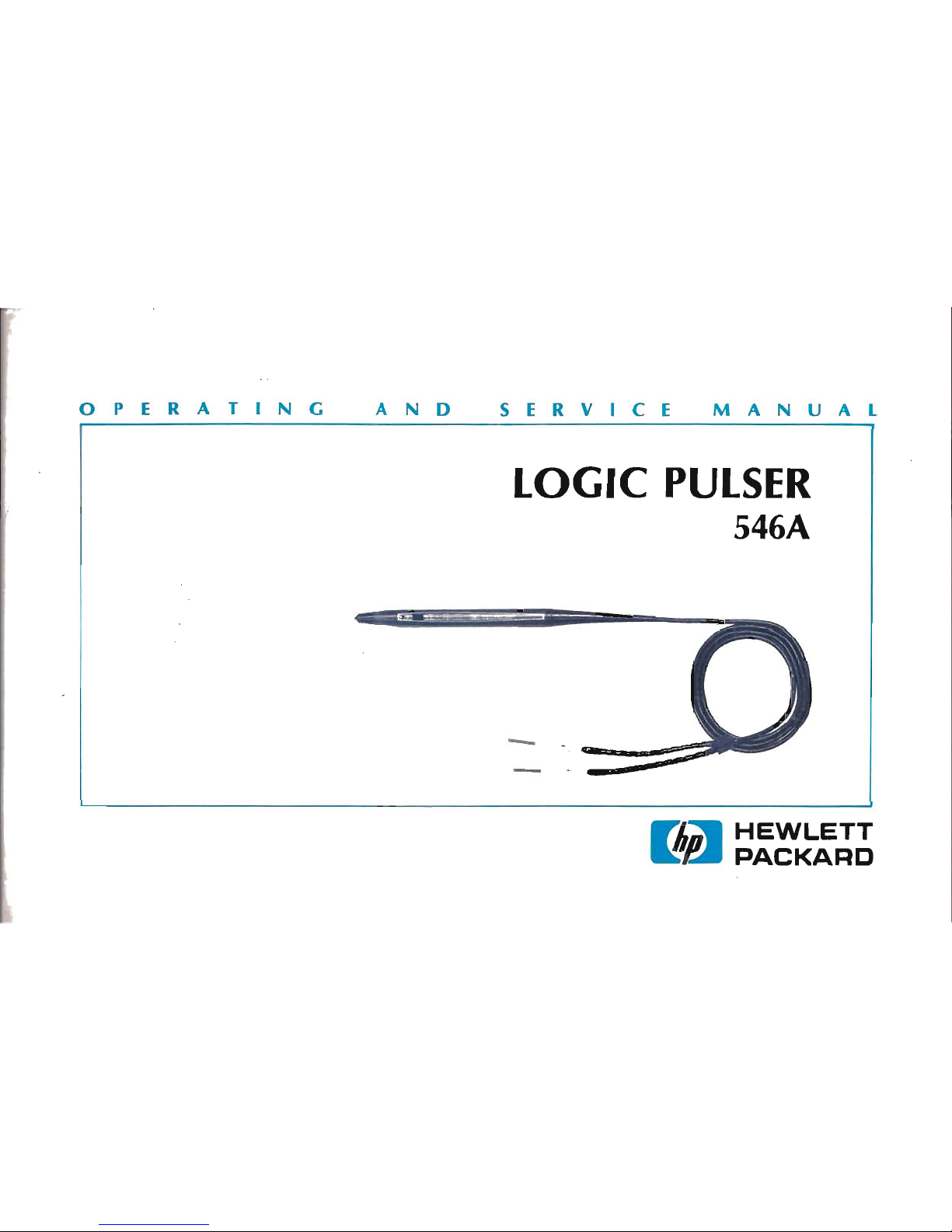
LOGIC
PULSER
546A
Flio-
HEWLETT
PACKARD
Page 2
HEWLETT-PACKARD
SALES
AND
SERVICE
OFFICES
To
obtain
servicing information and
order
replacement parts,
contact
the
nearest Hewlett-Packard Sales and
Service Office in
HP
Catalog,orcontact
the
nearest regional office.
IN
THE
UNITED
STATES:
CALIFORNIA
3939 Lankershim Blvd.
North Hollywood
91604
GEORGIA
P.O. Box
28234
450
Interstate North
Atlanta
30328
ILLINOIS
5500
Howard
Street
Skokie
60076
NEW
JERSEY
W.
120
Century Road
Paramus
07652
IN
CANADA:
QUEBEC
Hewlett-Packard (Canada) Ltd.
275 Hymus Blvd.
Pointe Claire
IN
EUROPE:
SWITZERLAND
Hewlett-Packard (Schweiz) AG
RueduBois-du-Lan 7
P.O. Box 85
CH-1217 Meyrin 2 Geneva
IN
AFRICA,
ASIA,
AND
AUSTRALIA:
Hewlett-Packard
Intercontinental
3200 Hillview Ave.
Palo Alto, California
94304
IN
CENTRAL
AND
SOUTH
AMERICA:
Hewlett-Packard
Intercontinental
3200 Hillview Ave.
Palo Alto, California
94304
Page 3

Hewlett-Packard
Company
certifies
that
this
instrument
met
its
published
specifications
at the time
of
shipment
from the factory.
Hewlett-Packard
Company
further
certifies that its
calibration
measure-
ments are traceable to the
United
States
National
BureauofStandards,tothe
extent
allowedbythe
Bureau's
calibration
facility,
and
to the
calibration
facilitiesofother
International
Standards Organi-
zation members.
WARRANTY AND ASSISTANCE
This
Hewlett-Packard
productiswarranted against defects in materials and
workmanship
for
a period
of
one
year
from the dateofshipment.
Hewlett-Packard
will, at its
option,
repairorreplace
products
which
prove
to be defective
during
the
warranty
period provided
they
are returned to
Hewlett-Packard,
and prOVided the preventive
maintenance
proceduresinthis
manual are followed. Repairs necessitated
by misuse
of
the
product
are
not
covered
by
this
warranty.
NO
OTHER
WARRANTIES ARE EXPRESSED
OR IMPLIED,
INCLUDING,
BUT
NOT
LIMITED
TO,
THE
IMPLIED WARRANTIES OF
MERCHANT-
ABILITY
AND
FITNESS FOR A
PARTICULAR
PURPOSE.
HEWLETT-PACKARDISNOT
LIABLE
FOR
CONSEQUENTIAL
DAMAGES.
Service
contractsorcustomer
assistance agreements are available
for
Hewlett-Packard
products.
For
any
assistance,
contact
your
nearest
Hewlett-Packard
Sales and
Service
Office. Addresses are
pro-
vided
at the backofthis manual.
010000-A-237
Page 4
This
change
supersedes
all
earlier
dated
changes.
***
Make
all
corrections
listed
under
ERRATA
before
making
other
changes.
********************
*
INSTRUMENT:
546A
*
*
Logic
Pulser
Operating
and *
*
Service
Manual *
* *
***
Check
following
table
for
your
instrument's
serial
prefix,
series
number,
or
date
code
and
make
listed
change(s)
to
manual.
*
*
SERIAL
PREFIX:
*
*
DATE
PRINTED:
*
HP
PART
NO:
*
MICROFICHE
NO:
* ********
1644
MAY
1977
00546-90005
00546-90006
*******
*
*
*
*.
*
*
* ***
n
INDICATES
NEWORREVISED
ITEM
>
INDICATES
ACTIONTOBE
TAKEN
00546-60100 ...1
Series
1732
SERIAL
PREFIX,
MANUAL
SERIES
NUMBER
OR
DATE
CODE
CHANGE(S)
thru
4
thru
5
thru
6
MANUAL
CHANGE(S)
..••1
thru
3
01A2132.
01A2312.
02A2312.
00546-60100 .
Series
2012
**
**
**
SERIAL
PREFIX,
**
SERIES
NUMBER
**
OR
DATE
CODE
**--------------------
**
**
**
**
**
...••
1,2
00546-60100
Series
2008
(C5460SX) 1=6809,6812/2=8886E/3=9712E/4=12414,12007/5=14585
Flin-
HEWLETT
PACKARD
MANUAL
CHANGES
MODEL
546A
(00546-90005)
Page
i
Insert
this
Warning
after
the
Certification/Warranty
and
Assistance
which
is
the
inside
front
cover.
WARNING
This
product
should
be
connected
to
a power
source
that
is.
sufficiently
isolated
from
the
main
supply
to
prevent
the
risk
of
electric
shock.
To
further
reduce
the
risk
of
electric
shock,
refer
to
the
service
manual
for
the
equipment
under
test
(when
applicable)
and
follow
the
manufacturer's
service
and
safety
precautions
particularly
when
voltages
exceeding
30
VRMSor50
VDC
are
present.
Page 5
i
#ERRATA
Page
30,
Figure
14,
NOTE*:
>Change
note
to
read
"MP3
NOT
USEDINALL
PULSERS.
SEE
PAGE
33."
Page 33,
Table
6,
Replaceable
Parts:
>Change
HP
part
number
for
A1R4
to
0686-1325.
Page 36,
Figure
16,
A1
Schematic
Diagram:
>Add
two
short
parallel
arrows
adjacent
to
DS1
to
indicate
a
light
emitting
diode.
>Change
NOTE3to
"U1
PIN
12
MAYBECONNECTEDTOCOMMONINSOME
PULSERS".
>Add
"+"
symbol
adjacent
to
top
terminal
of
C2
to
indicate
the
positive
side
of.
the
electrolytic
capacitor
for
C2.
Page 32,
Table
6,
Replaceable
Parts:
>Change
A1MP1
from 00546-20202
to
0570-0662
in
HP
Part
Number
and Mfr.
Part
Number
columns.
CHANGE
1 (00546-60003
Series
1732)
NOTE
--
The
circuit
board
is
changed
mechanically
to
incorporate
an improved
push
switch.
The
new
00546-60003
circuit
board
is
electrically
identical
to
the
00546-60002
SERIES
1644
circuit
board.
Page 6
CHANGE1(cont'd)
Page
30,
Figure
14,
Pulser
Disassembled:
>Change
MP4toMP14.
>Change
MP5toMP15.
>Change
MP8toMP9.
Page
32,
Table
6-1,
Replaceable
Parts:
>Change
A1
part
number from 00546-60002
to
00546-60003
for
HP
& Mfr.
Part
No.
>Change
A1
Series
number from 1644
to
1732.
Page 33,
Table
6,
A1
(00546-60100)
Replaceable
Parts:
>Change
A1S1
from 00546-00001
to
0546-00002
in
HP
and Mfr.
Part
Number
columns.
Page
33,
Table
6,
Miscellaneous
Parts:
>Change
MP4toMP14
and
Part
Number
in
HP
and Mfr. columns from 00546-20201
to
00546-20202.
>Change
MP5toMP15
and
Part
Number
in
HP
and Mfr. columns from 00545-20203
to
00545-20205.
>Change
MP8toMP9
and
Part
Number
in
HP
and Mfr. columns from 00546-40001
to
00546-40004.
>Add
MP10;
00546-40003;
RETAINER-SWITCH,
BLK
PLASTIC;
28480; 00546-40003.
>Add
MP11;
0624-0340; 2;
SCREW-SELF
TAPPING
0-42
(MP10
MTG);
28480;
0624-0340.
>Add
MP12;
7120-5268;
NAMEPLATE;
28480; 7120-5268
(BOTTOM
HALF).
>Add
MP13;
7120-5274;
LABEL-OPERATING:
28480; 7120-5274
(TOP
HALF).
-
Page 7
1-
I
CHANGE1(cont'd)
Page 36,
Figure
16,
A1
Schematic
Diagram:
>Change
HP
Part
Number
for
A1
from 00546-60002
to
00546-60003
SERIES
1732.
>Add
to
arrows
by
DS1
to
indicate
a
LED.
>Change
"U1
PIN
2"
in
NOTE3to
U1
PIN
12.
CHANGE
2 (00546-60003
Series
200B)
Page 32,
Table
6,
Replaceable
Parts:
>Change
A1
from
series
1732
to
200B.
>Add
A1CB;
0160-0576;
CAPACITOR
FXD
0.1UF
20%
50VDC
CER;
26654;
2130BR050R104M.
Page 36,
Figure
16,
A1
Schematic
Diagram:
>Change
A1
series
number from 1732
to
200B.
>Add
0.1u
capacitor
CB
across
power
supply
input
between
emitter
of
Q3
and
circuit
board
common.
CHANGE
3 (00546-60003
Series
2012)
Page
32,
Table
6,
Replaceable
Parts:
>Change
Al
from
series
2008
to
2012.
>Change
A1C1
(0160-4422)
to
0160-5238;
CAPACITOR-FXD
.B2UF
20%
50VDC
DISC
CER.
Page 36,
Figure
16,
Al
Schematic
Diagram:
>ChangeAl
Series
from 2008
to
2016.
>Change
A1Cl
from
1uf
to
.82uf.
Page 8
I
HCHANGE
4
Title
Page
SERIES
NUMBERS
NOT
LISTED:
>Change
to
read
as
follows:
For
Logic
Pulsers
with
series
numbers
higher
than
1644,
or
with
condensed
Series
Numbers
provided
on
the
Date
Code
label,
a
MANUAL
CHANGES
sheet
is
included
with
this
manual. For
series
numbers below 1644,
refer
to
the
Backdating
paragraph
in
this
manual.
Page 1
SERIES
NUMBER:
>Delete
the
paragraph
under
"SERIES
NUMBER".
>Replace
with
the
following
information:
SERIES/DATE
CODE
This
product
is
identified
byaSERIES
CODE
and
DATE
CODE,
located
on a
vinyl
label
affixed
to
the
inside
of
either
the
top
or
bottom
of
the
pulser
shell.
The
Series/Date
Code
format
used
in
all
logic
probes
is
as
follows:
"01A2132"
The
first
two
digits
represent
a
condensed
Series
Code.
When
a change
occurs
to
any model
of
HP
logic
probe
family
which
affects
the
schematic,
parts
list,
or
specifications,
the
condensed
SERIES
CODEisincremented
by
one.
The
letter
"A"
designates
the
country
of
origin;
"A"
indicates
USA.
Page 9
I
CHANGE4(cont'd)
The
last
four
digits
represent
the
Date Code.
The
Date
Code
identifies
the
date-of-manufacture
for
the
pulser.
The
first
two
digits
indicate
the
year
the
product
was
manufactured;
the
last
two
digits
indicate
the
week
of
that
year.
Datecoding
originated
in
the
year
1960,
at
which
time
the
code
"00"
was used
for
the
first
two
digits
to
represent
1960. Every
year
after
1960
the
code
was
incremented
by
one;
for
example,
the
Date
Code
"2012"
indicates
the
product
was
manufactured
in
the
12th
week
of
the
year
1980
(1960+20).
Your
pulser
will
have
either
a
four-digit
Series
Number
stamped
on
the
printed
circuit
board
or
a condensed
Series
Code,
prefixing
the
Date
Code
on
a
vinyl
label
affixed
to
the
inside
of
the
pulser
shell.
WHICH
CHANGES
APPLYTOYOUR
LOGIC
PULSER?
There
isaSERIES/DATE
CODE
number
listed
on
the
cover
of
the
MANUAL
CHANGES
sheet.
As
changes
are
made,
the
condensed
Series
Code
is
incremented
by
one.
Make
all
changes
to
your manual
for
Series
Codes
less
than
or
equal
t(
your
pulser
Series/Date
Code.
CHANGE
5
Page 32 and 33,
Table
6.
Al
(00546-60003)
Replaceable
Parts:
>Change
C6
from 0160-4343
(.lUF)
to
0180-0291
lUF
+-10%
35
VDC
TA.
>Change
R3
from 0698-7284
(lOOK)
to
0698-7260
10K
1%
.05WFTC=O+-100.
Page 36,
Figure
16.
Al
Logic
Pulser
Assembly
Schematic
Diagram:
>Change
the
value
for
C6
from .1UF
to
lUF.
>Change
the
value
for
R3
from
lOOKto10K.
IICHANGE
6
On
the
Title
page,
Change
the
Configuration
Code
from
01Ato02A.
Page 10
-
..
_------
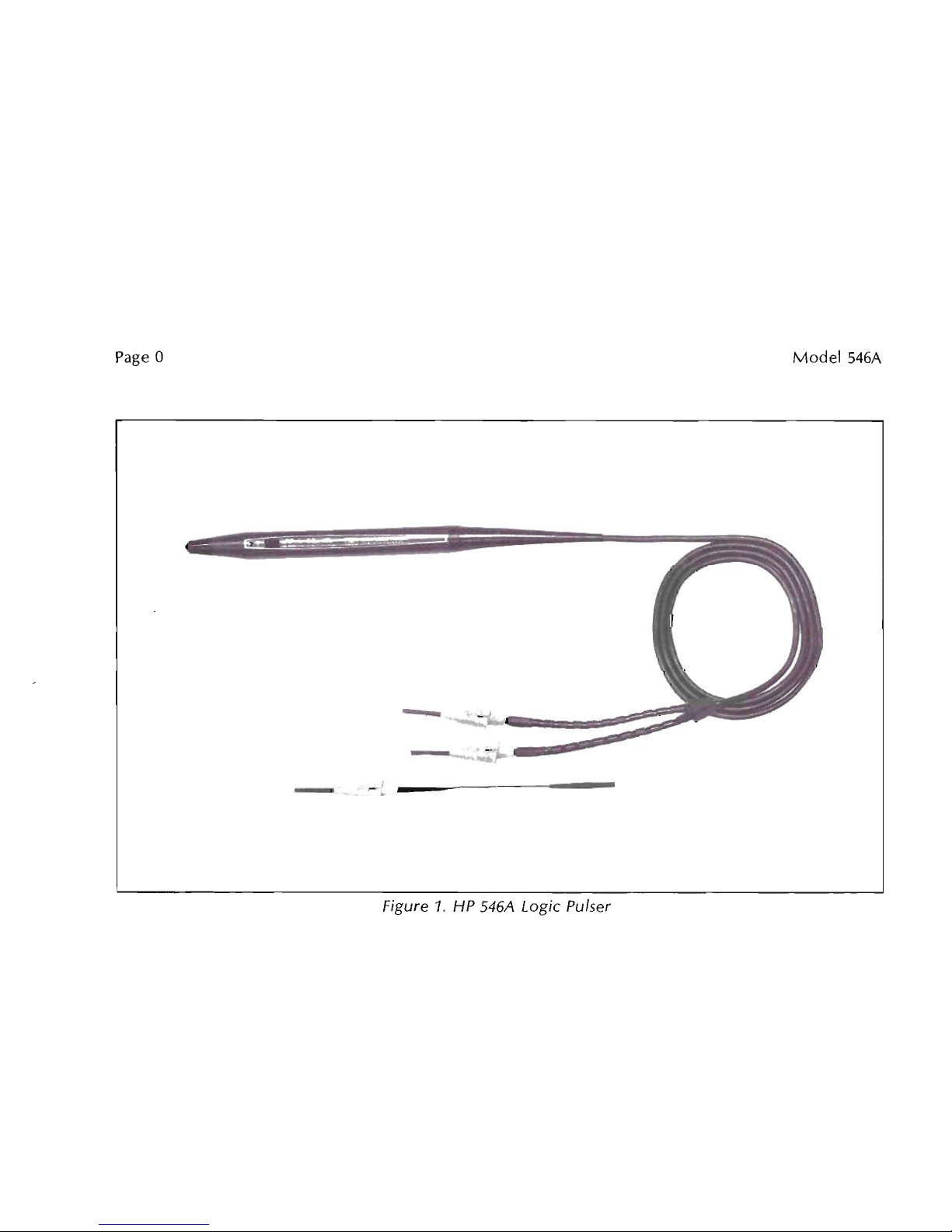
Figure1.HP
546A
Logic
Pulser
Page 11
SCOPE
OF
MANUAL
This manual provides
operating
and service
information
for
the
Hewlett-Packard
Model
546A
Logic
Pulser (Figure 1). The
information
includes a descriptionofthe
Logic Pulser, accessories available,
specifications, unpacking,
operating
characteristics,
operating
procedures, applications, theory
of
operation,
maintenance, replaceable parts, and a schematic diagram.
DESCRIPTION
The
HP
546A
Logic Pulserisa
hand-held
logic
node
stimulator
used
for
injecting
controlled
pulses
into
digital logic circuits. The electronics are housed in a
hand-held
probe.
Automatic
pulse
control
is
prov'ided
for
TTL,
OTL,
RTL,
HTL,
MaS,
and
CMOS
logic. Pulse
amplitude
depends
on
the logic
supply voltage (3-18V)
whichisalso
the
supply voltage
for
the Logic Pulser. Pulse
current
and pulse
width
depends on the load
being
pulsed. The
frequency
and
number
of
pulses generated by the
pulser
is
controlled
by
operationofa push-slide switchonthe pulser
probe.
A flashing
LED
indicator
located in the
tip
indicates
the
output
mode.
Refer
to
Table 1
for
Logic Pulser specifications and to
Figure 2
for
accessories available.
SERIES
NUMBER
The Logic Pulser does
not
have a serial
number.Itdoes have a
four
digit
series
number,
which
is
stamped on the
printed
circuit
board. Refer to this
number
and the
circuit
board part
number
in any
correspondence
pertainingtomaintenance.
Page 12
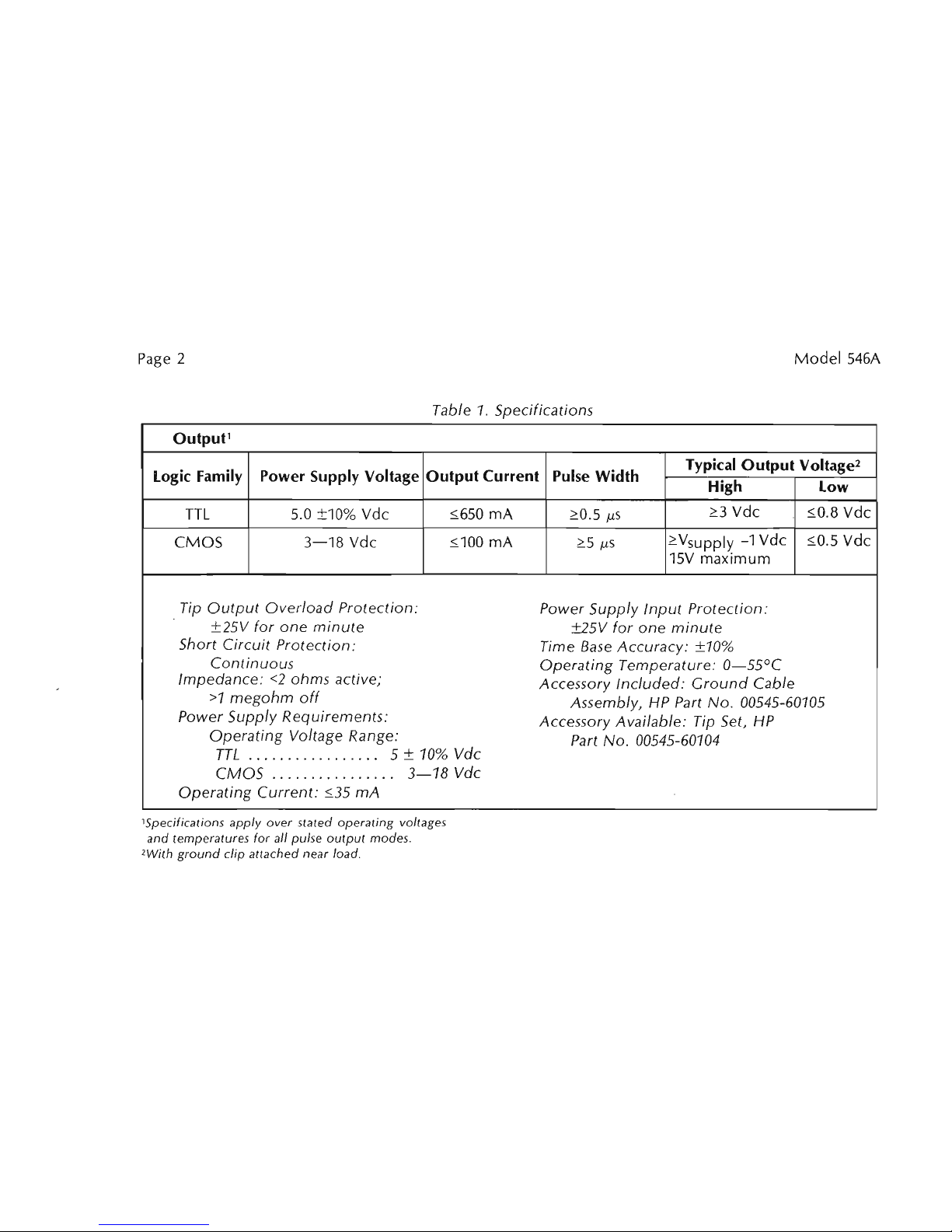
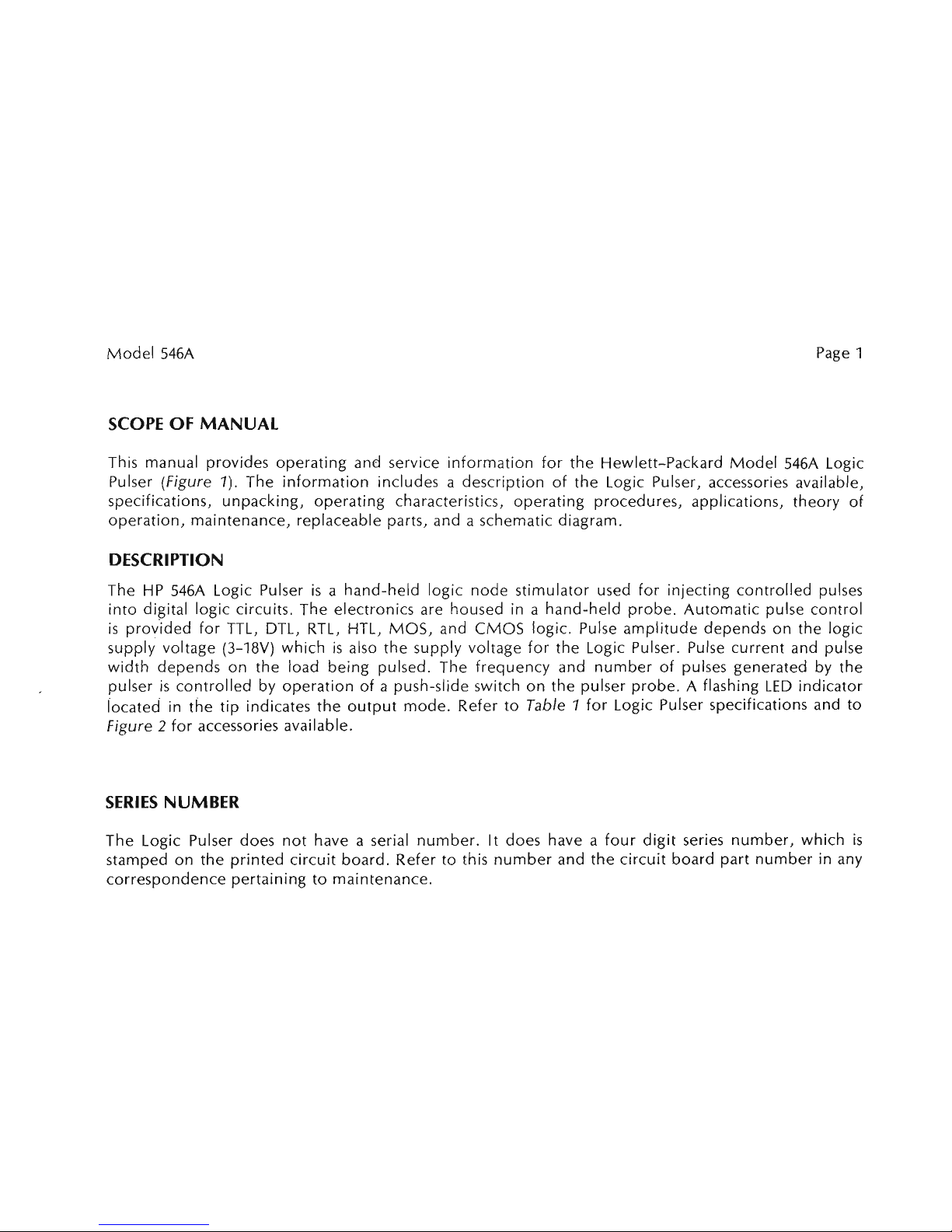
Table1.Specifications
Output'
Logic
Family Power Supply Voltage
Output
Current
Pulse
Width
Typical
Output
Voltage
2
High
Low
TTL
5.0 ±10%
vdc
:5.650
mA
?0.5
j.ls
?3
vdc
:5.0.8
Vdc
CMOS
3-18
vdc
:5.100
mA
?5
j.ls
?Vsupply-1vdc
:5.0.5
vdc
15V
maximum
Tip
Output
Overload
Protection:
Power Supply
Input
Protection:
±25V
for
one
minute
±25V
for
one
minute
Short
Circuit
Protection:
Time
Base
Accuracy:
±10%
Continuous
Operating
Temperature:
0-55°C
Impedance:
<2 ohms active;
Accessory
Included:
Ground
Cable
>1
megohm
off
Assembly, HP Part No. 00545-60105
Power Supply
Requirements:
Accessory
Available:
Tip Set,
HP
Operating
Voltage Range:
Part No. 00545-60104
TTL
.................
5±
10%
vdc
CMOS
................
3-18
vdc
Operating
Current:
:5.35
mA
'Specifications
apply
over
stated
operating
voltages
and
temperatures
for
all
pulse
output
modes.
2With
ground
clip
attached
near
load.
Page 13
Tip
Kit:
00545-60104
10526-60002
Multi-Pin Stimulus
Kit
Figure2.546A
Logic
Pulser Accessories
Available
Page 14

UNPACKING
If
the
shipping
packageisdamaged,
ask
that
the
carrier's agent
be
present
when
the package
is
opened.
Inspect
the
Logic Pulser
for
obvious
physical damage (dents, scratches, etc.). If
the
Logic
Pulser
is
damaged
or
fails
to
meet
specifications,
notify
carrier and nearest Hewlett-Packard
Sales
and Service
office
immediately.
(Sales
and Service offices are listedatthe
backofthis manual.) Re-
tain
shipping
package and packaging material
for
carrier's inspection. The
Sales
and Service
office
will
arrange
for
replacement
of
your
Logic Pulser
without
waiting
for
claim against carriertobe
settled.
POWER
SUPPLY
The
power
leads are
connected
to
the
power
supplyofthe
logic
being
pulsed(3to
18V). Reverse
polarity
and excess voltage
protection
are
provided.
The red
power
leadisconnectedtothe
positive
side
of
the
power
supply.
OUTPUT
GROUND
CABLE
A
connector
for
the
ground
cable
providedislocatedatthe
tipofthe
Logic Pulser.
When
maximum
current
outputisdesired,
use
the
ground
cable supplied
with
the
Pulsertomake
the
common
return
path
as
shortaspossible.
Current
pulses
from
the
Pulser can be
more
than
650
mAo
The
ground
cable
reduces the
IR
drop
and
the
lead
inductance.
Page 15
OPERATING
CHARACTERISTICS
The HP 546A Logic Pulser generates pulses
as
programmed
by a
fingertip
push-slide switch. The
Pulser
is
programmed
by
pushing
the
switch
once
for
each single pulse
output,
or
a specific
number
of
times
for
continuous
pulse streamsorpulse bursts at selected frequencies. The
numberoftimes
to
push
the
switchtoselectanoutput
modeislabeled adjacenttothe
switch andisdescribed in Table 2.
On
the
label a
dot
(e) represents a push; a dash
(-)
represents a
hold.Asshown in Table 2,
the
pulses
appliedtothe
LED
indicatorsinthe
tip
are slowed
down
for
visibility.
Pressing
the
switch
automatically
drives a TTL, DTL,orCMOS
logic
output
or
input
from
LOW
to
HIGHorfrom
HIGHtoLOW.
The
high
source and sink
current
capabilityofthe
Pulser can
override
integrated
circuit
output
points,
originallyineither
the
HIGHorLOW
state. The
nominal10jJ.s
pulse
width
is
long
enough
for
even slow
CMOS
circuitstoaccept,
but
heavy
circuit
loads (suchasTTL
drivers) result in
narrower
pulses that
limit
the
amountofenergy
deliveredtothe
device
under
test.
The Pulser's
outputisthree-state. In
the
off-state,
the
probe's
high
output
impedance
ensures that
circuit
operationisunaffected
by
probing
until
the
Pulser switchispressed. Pulses can
be
injected
while
the
circuitisoperating
and
no
disconnections
are
needed.
The
multi-pin
stimulus
kit
(Figure
2)
is
useful
for
stimulating
uptofour
inputsofa gate at
the
same
time,orfor
stimulating
four
different
circuit
nodes.
The Pulser's
power
input
and
output
(tip)
circuits are
protected
against
overvoltage
and reverse
polarity.
Page 16
Switch Action
Output
Pulse Rate
Output
Pulse
Mode
LED
Indication
(±10%)
Push
single
1 Pulse
One
short
flash
Push-hold
100 Hz 100 Hz
(Continuous)
10
Hz
rate
Push/push-hold
100 Hz 100
Burst.
10 Hz
rate
during
burst
Push/push/push-hold
10 Hz 10 Hz
(Continuous)
5 Hz
rate
Push/push/push/
100 Hz
10 Burst •
Two
short
flashes
and
push-hold
a
l-second
pause
Push/push/push/
1 Hz 1 Hz
(Continuous)
One
flash/second
push/push-hold
• 1
second
burst
for 100
pulses
every
two
seconds
.
• 0.1
second
burstof10
pulses
once
each
second.
(
0
1
10
Hz
rrn,ill
546A
LOGIC
PULSER
]
z
100
-
'0
BURST
.. -
0
100
aURST . ,
H'
....
HEWLETT·PACKARD
Page 17
A push-push action
of
the switch must
occur
within
less
than 1 second to be effective.
A
hold
actionofthe
switch
for
greater than 1 second begins executionofthe
pro-
grammed
output.
Any
function
can be locked on by the push-slide actionofthe
switch.
Releasing
the
switch
midway
through
a burst does
not
terminate
the
burst.
The single pulses generated
when
a burstisprogrammed
are subtracted
from
the
first burst, e.g., a
100
burstisoutputas1-1-98, lOa, lOa, etc.
Releasing the switch in any
output
mode
other
than
midburst
terminates
output
and allows a
new
mode
to
be
programmed
immediately. Releasing the switch
for
longer than 1 second, erases the
programmingofprevious pushes.
(3)
(4)
(5)
(6)
OPERATING PROCEDURES
To operate the Pulser, observe
the
following
procedures:
NOTE
In the
following
step, be sure to
connect
the red
power
leadofthe Pulser
to
the positive sideofthe
powersupply.
a.
Connect
the
power
leads
of
the
pulser
to
the
power
supply
of
the
logic being pulsed
(3to18V). (The Pulser may be
powered
fromadifferent
source,
provided
the voltageisthe
same
as
thatofthe
circuit
under
test and a
common
groundisused.)
b.
Contact
the
logic
nodetobe stimulated
with
the
tipofthe
Pulser.
c.
program the generation
of
pulses by pushing
the
switch
per
adjacent markings (refer
to
Table 2
for
details). Characteristicsofthe
switch
operation
are described in the
following
steps.
(1)
(2)
Page 18

ing
the
lamp flash bursts allows
controlofa precise
numberofoutput
pulses.
APPI.ICA
liONS
Hewlett-Packard makes several instruments
which
assist
the
troubleshooter
in testing logic circuitry
with
the Logic Pulser. These instruments are listed in Table 3 and examplesoftheir
applications are
given in
the
following
paragraphs.
Table3.Logic
Test
Instruments
. Typical Digital
Ie
HP Instruments
Troubleshooting
Stimulus
Response
Shorted IC
Input
546A Pulser
547A
Current
Tracer and
545A Logic Probe
Stuck Data
Bus
546A Pulser
545A Logic Probe and
547ACurrent
Tracer
Internal
Open
in IC
546A Pulser
545A Logic Probe
Solder Bridge
546A Pulser
547A
Current
Tracer
Sequential Logic Fault
546A Pulser
548A Logic
Clip
ShortstoVccorGround
546A Pulser
545A Logic Probe
Multi-Pin
Testing 546A Pulser 10529A Logic
Comparator
Page 19

Logic Gate Testing
A logic gate may be tested by pulsing the gate's
input,
while
monitoring
the
output
with
a Logic Probe
(see
Figure 3). The Logic Pulser generates a pulse opposite
to
the stateofthe
input
line and can
change the gate
output's
state. This assumes the
outputofthe gateisnot
clamped in its state by an-
other
input,
e.g., a HIGHonthe
other
inputofan
OR gate.
SL
SL
NO
CHANGE
OF
STATE, INVERTER
IS FAULTY
GATE UNDER
TEST
Figure3.Logic
Gate
Testing
Page 20

If
the pulseisnot
detected at the
output,
pulse the
output
line
(see
Figure
4).
If the
outputisnot
shortedtoVccor
common
return,
the Logic Probe should indicate a pulse opposite to
its
original
indi-
cation.Ifnot,
check
for
external shorts (solder bridges, etc.)
before
removing the integrated circuit.
Refer also
to
Gate-to-Gate Faults paragraph.
I
I
H
L
PROBE
PULSE SWITCH
IS
PROBE
LIGHT
DOES NOT
CHANGE
STATE:
LINE
IS SHORTED
TO
Vee
OR
GROUND.
Figure4.Testing
for
Shorts
Page 21

Counter, Shift Register, and Flip-Flop Testing
MSI
Ie's,
suchasshift registers and counters, typically have several
output
pins
where
data must be
monitored
when
testing. The Logic Pulser, usedasa manually
controlled
clock, allows the Logic Clip
to simultaneously examine all
output
dataatrates
convenient
for
viewing.
When
the Logic
Clipisplaced
on
an
IC, the
LED's
on
the
clip
indicate the logic stateofeach
pin
(see Figure 5).Asthe Pulser
clocks . the
input,
the
indi-
cationsonthe
Clip
can be
com-
paredtoa
truth
table.
Figure
5.
Multi-pin
Testing
with
Logic
Clip
Page 22

The 10529A Logic
Comparator
(Figure6)is
an
IC
troubleshooting
tool
that electrically compares a
reference IC
to
an
IC
under
test. The reference IC shares the
power
and
input
signals
with
the test
Ie.
When
comparing the outputsofthe
two
Ie's,
any level
difference
existing
for
0.2
j.lsormore
will
lightanLEDonthe comparator, thereby indicating a fault.
The Logic Pulser allows
in-cir-
cuit
stimulation,
so
test pulses
may be
introduced
at
circuit
nodes. Thus, resetorsynchro-
nizing pulses may be injected
to
reset the comparator's IC to
the
same initial stateasthe test
Ie.
This allows the reference IC
and
the
test ICtobegin
oper-
ation
from
the same reference
point.
Figure6.Multi-pin
Testing
with
Logic
Comparator
Page 23

Wire-AND
Node
Oneofthe
most
difficult
problems
encounteredintroubleshooting
integrated
circuitsisa stuck
wire-
AND
node.
Typically J
oneofthe
open-collector
gates may still
continue
sinking
current
after it
has
been
turned
off.
The Logic Pulser and
Current
Tracer
providesaneasy
methodofidentifying
the
fault
gate.
Referring
to
Figure 7 place
the
Current
Traceronthe
gate sideofthe
pull-up
resistor.
Align
the mark
on
the
probe
tip
along
the
lengthofthe
printed-circuit
trace and adjust
the
probe's
sensitivity
control
until
the
indicatorisjust
fully
lighted.Ifthe
indicator
will
not
light
- use a Logic Pulser
programmed
to
the.100 Hz
continuous
modetoexcite
the
line.
Place
the
tracer
tip
on
the
output
pinofeach gate;
only
the
faulty gate
will
cause
the
indicatortolight.
Gate-to-Gate
Faults
Whenalow-impedance
fault
exists
between
two
gates
J
the
Current
Tracer and Logic Pulser
combine
to
quickly
pinpoint
the
defect.
In Figure 8 gate A's
outputisshorted to
ground.
Place the pulse
mid-
way
between
the
two
gates and place
the
Current
Tracer's
tiponthe
Pulser's
pin.
Pulse
the
line in
the
100
Hz
continuous
mode
and adjust
the
Current
TracerJs
sensitivity
control
until
the
indicator
just
lights. First place
the
Current
Tracer
tip
nexttogate A and
then
gate B
while
continuing
to excite the
trace. The tracer
will
light
only
on
the
gate A sideJsince gate AJ(the
defect
in this example),issink-
ing
the
majorityofthe
current.
Page 24

+5V
LOGIC PULSER
(IF NECESSARY)
CURRENT
PATH
TRACER
WILL
LIGHT
HERE
BUT NOT ON OTHER GATES
Figure7.Wire-AND
Node
Fault
Page 25

LOGIC
PULSER
CURRENT
TRACER
THE
MAJORITYOFPULSE CURRENT
"oWS'"W'''coYcmA
]
I
¢
Figure8.Gate-to-Gate
Faults
LOGIC
PULSER
Page 26

The
major
circuitsofthe
Pulser are
contained
in integrated
circuit
U1asshown in
Figure
9.
Operating
voltageissupplied by a
power
supply and
outputs
are senttothe
output
drive
circuits andtothe dis-
play LED's.
Power Supply
The
power
supply converts
thedcinput
voltagetoa regulated voltage
for
low
power
logic. The
circuit
provides reverse voltage and overvoltage
protection.
Integrated Circuit U1
Several
functions
are
provided
by
U1asdescribed in
the
following
paragraphs.
VOLTAGE REGULATOR. Provides voltage and
temperature
compensated reference and
control
cir-
cuitry
for
the
low
voltage
logiconthe
Ie.
MODE
SELECT
CONTROL
Determines
whether
the
instrumentisprogrammingamodeorexecut-
ing a
mode
and
whentoreset.
SWITCH INPUT
CONTROL
Presets
the
time
base/counter
and burst
control
circuit;
generates a
single-shot pulse
to
the
output
and
debounces
the
switch.
Page 27

L
I---
TIP
OUTPUT
DRIVE
CIRCUITS
DISPLAY
'"
I/
I
DISPLAY
DRIVE
MODE
SELECT
CONTROL _
I
L
/1"
I
-Ir-"-R-O-M
.......: ...-__-_-_-_
-....,
0"""
I
,..
CONTROL
-,
L
f--
I
I
I L '-----' I
I I
1-
BURST TIME BASEl
"+-t-t----l
I _ COUNTER r CLOCK I
I I
POWER
SUPPLY
k--------:=I
I
VOLTAGE
REGULATOR
V+
Figure9.Pulser
Block
Diagram
Page 28

BURST
CONTROL.
Controls
the
start, stop, and
countofa burst.
DISPLAY
DRIVE.
Controls
the
LED
displaytoindicate
Pulser activity.
ROM. A 256-bit special purpose
read-only-memory
that
controls
the
operationofthe Pulser.
TIME
BASE/COUNTER.
Usedastime
base
for
the
ROMtogenerate the 1, 10, and
100Hzcontinuous
stream pulses,asa
counter
for
the
burst counts and
for
overall system
timing.
CLOCK.
Free-running
100
Hz
RC
controlled
clock actsasa
time
base
for
operationofthe
Pulser.
OUTPUT. Provides single positive and negative pulses at
controlled
rates, widths, and levelstothe
output
drive
circuits.
Senses
the
charge
deliveredtothe
external load and
will
automatically terminate
(shutdown),anoutput
that exceeds a
predetermined
limit.
Detailed Circuit Analysis
As shown in
Figure
16, transistor
Q3isa series
pass
element
for
a voltage
regulatorinUl
which
generates a 2.7
volt
reference
voltage. Resistor
R4
acts
as
a series
pass
helper
resistor,
diverting
someofthe heat
normally
generated in
Q3,
especially at high voltage. Capacitors
C5
and C7 act
as
low
impedance
filter
capacitors
to
the
2.7
volt
supply. The
LED
for
DSlisdriven
by a switchable
constant
current
driver
on
U1
to
indicate
the
output
mode.Adifference
exists
between
the
light
output
of
the
LED
and
the
tip
output
of
the
probe.
Since
the
human
eye
cannot
see a
100
Hz,
10
J.ls
blink,
the
LED
pulses are actually slowed
down
and stretched,
driving
the
LEData slower
rate,
indicating
the
particular
activity at
the
tip. Switch
S1isused
to
program
the
modeofU1.
Resistor
R3
and capacitor C6 are
the
timing
elements
that
control
the
accuracy and
frequency
of
the
voltage and
temperature
compensated 100
Hz
clock in
Ul.
Page 29

OUTPUT
STAGE.
(Pins 2,1,16,15.)
Capacitor
C2isa charge storage
capacitor
thatischarged
through
an
internal
resistortothe
supply
voltage
(V+j,
the
"1"
output
level. This capacitor allows
the
Pulser
to
delivery
high
output
current
without
causing heavy surges
on
the
power
lead. Breakdown
diode
CRl
protects
Ul(l)
from
high
voltages. Transistor
Qlisthe
drive
transistor
for
the
logic
"1"
pulse and
Q2isthe
drive
transitor
for
the
logic
"a" pulse.
CapacitorCland resistorRlare
coupling
elements
to
the
tipofthe
probe.
CapacitorCldecouples
highdclevels
from
the
tipofthe
probetothe
output
cir-
cuitry
and also actsasan
overload
sensing
element,
activating
the
shutdown
circuitryinUl
(pin 16).
Between
output
cycles resistor R1 discharges any residual chargeoncapacitor
Cl.
ResistorR2limits the
current
into
Ul
on
this sense
line,
and capacitor
C3isa
speedup
capacitor. Capacitor C4
on
pin
14
controls
the
normal
output
pulse
width
of
both
the
"1"
and "a"
throughaone-shotinUl,
typically
10).Ls
(may vary
between
5-15
).Ls).
ResistorR5stabilizes
the
output
stage.
Overcurrent
Output
Shutdown
If
the
circuit
under
test presentsanoverloadtothe
Pulser's
output,
a sensing
circuit
within
Ul
causes
the
overcurrent
shutdown
cycletooccur
and
turn
off
the
output
transistor.Ifthe
overload
presents a
low
impedance
to
V+,
the
"a"
overcurrent
cycle occurs.Ifthe
load presents a
low
impedance
to
ground,
the
"1"
overcurrent
cycle occurs. These cycles are described in
the
following
paragraphs.
Waveforms
of
the
overcurrent
conditions
are
shown
under
test
procedure
paragraphs.
Immediately
priortoany
output
pulse cycle, capacitor C2ischargedtoV+,
capacitorClis
discharged
by resistor
Rl
to
avolts, transistors
Ql
and
Q2
are
off
and
Ul
pin16isatthe
tip
voltage.
Page 30

U1
(pin
16)
begins measuring
voltage
on
the
tip
through
resistorR2and capacitor C3.
With
transistor
Q2
conducting
heavy
current
from
the
load
through
the
tip,
capacitor C2 develops a voltage charge.
When
this voltage reaches
approximately
0.8 volts (relativetoground)
pulse
shutdown
occurs in
the
U1
sensing
circuit
and transistor
Q2
turns
off.
"1"
OVERCURRENT CYCLE. The
"1"
cycleissimilar
to
the
"0"
cycle except that transistor
Q1
saturates,
the
direction
of
current
flowisreversed and
the
shutdown
threshold
voltageisreferenced
to
V+
(set to
approximately
V+
minus
1.5 volts).Inaddition,
capacitorC2supplies mostofthe
output
current
through
transistor Q1 thus
reducing
current
surges
on
the
V+
line.
In
either
overcurrent
cycle
the
fast
turn
on
and
turn
offoftransistors Q1 and
Q2
provides sharp pulse
edge transitions
through
logic
threshold
transition
regions. The
"1"
or
"0"
overcurrent
output
cycle
is
repeated each
timeahigh
current
pulseisoutputted.
MAINTENANCE
The
following
paragraphs
provide
test
procedures,
probe
disassembly and assembly and parts re-
placement
information.
Test Procedures
The
following
performance
tests ensure that
the
Pulserisoperating
properly.
Test
equipment
re-
quiredislisted in Table4.Test
equipment
having
equivalent
characteristics may be substituted.
Page 31

NOTE
The
HP
180C
oscilloscope
listed in Table 4isrecommended
as a usually
available
type.
However,astorage
scope
suchasthe
HP
181Aispreferable
to
use
for
the
performance
tests.
Table4.Test
Equipment
Required
Instrument
Required Characteristics
RecommendedHPType
Oscilloscope
35
MHz,10mV/div,
0.1
I.<s/div
180C/1807A/1821A
Power
Supply
0-20V,O-lA
6201B
Counter
0-10
MHz
5300B/5301A
Resistor
TRMR, 200, 10%
2100-2413
Resistor
6.2.0, 5%, .25W
0683-0625
Resistor 3.6.0, 5%, .25W
0683-0365
Resistor
(2)
lK,
5%, .25W
0683-1025
Capacitor
10
MF,
±10%,
20V
0180-0374
Page 32

Functional Output Test
Using the test setup shown in Figure 10,
proceedasfollows:
a.
Set
power
supplyto+5V.
b.
Press
Pulser
pushbutton
and latch
(100
Hz mode)
while
observing oscilloscope
for
the wave-
form
shown in Figure 10.
c. The Pulser
LED's
should
flash
once
when
the
pushbuttonispressed and
continuously
when
the
switchislatched.
d. Repeat step (b)
while
varying
the
power
supply
output
over
the
rangeof3to18
volts and
check
waveform.
Change
the
scope vertical scale
factorasrequired.
The
output
pulse
width
will
normally
decrease in
the15to18volt
range.
"0"
Output Pulse at
5V
Test
Connect
the
equipmentasshown
in
Figure
11
and
proceedasfollows:
a.
Set
the
power
supplyto+5V.
b.
Press
Pulser
pushbutton
and latch
while
observing oscilloscope
for
the waveform shown in
Figure 11.
Page 33

l80C/
l807A/1821A
SCOPE
NOTE:
KEEP
LEADS SHORT
rnrn
546A
+5V
62018
POWER
SUPPLY
1V/DIV
5/LS/DIV
OV
Figure
10.
Functional
Output
Test
Page 34

6.2.11
180e/
1807A/1821 A
SCOPE
10M.
20V
iIJJ]]
546A
+5V
62016
POWER
SUPPLY
lV/DIV
O.51J.S/DI V
NOTE:
KEEP
LEADS
SHORT
OV
Figure 11.
"0"
Output
Pulse
at
5V Test Setup
Page 35

"0"
Output
Pulse
at 12V Test
Connect
the
equipmentasshown in
Figure
12
and
proceedasfollows:
a.
Set
the
power
supplyto+12V and set
the
variable resistorto200
ohms.
b.
Press
Pulser
pushbutton
and latch
while
observing oscilloscope
for
waveform
A,
Figure
12.
"0"
Output
Pulse
at 12V and Variable
Load
Test
Connect
the
equipmentasshown in
Figure
12
and proceedasfollows:
a.
Set
the
power
supplyto+12V.
b.
Press
Pulser
pushbutton
and latch.
c.
Set
the
variable resistortothe
values listed
below
while
observing the oscilloscope
for
the
out-
puts shown in
waveformBfrom
lefttorightinorderofthe
values listed
below:
10
ohms
50
ohms
100
ohms
200
ohms
Page 36

62018
0-200.11
+12V
POWER
r----..f)N'--------------------=-----l
SUPPL Y
180e!
1807A!1821A
seOPE
NOTE: KEEP LEADS SHORT
546A
2V/DIV
2/lS!DIV
OV
B
2V!DIV
2/lS!DIV
OV
Figure
12.
"On
Output
Pulse
at
12V
Test Setup
Page 37

"1"
Output Pulse Test
Connect
the
equipmentasshown
in
Figure
13
(except
omit
the
counter)
and
proceedasfollows:
a.
Set
the
power
supplyto+5V.
b. Set
the
variable resistorto0 ohms.
c.
Press
Pulser
pushbutton
and latch
while
observing
oscilloscope
for
waveform
A,
Figure 13.
d. Set
power
supplyto+12V and variable resistorto200
ohms
while
observing oscilloscope
for
waveformB,Figure
13.
e. Set
the
variable resistortothe
values listed
below
and observe
the
oscilloscope
for
the
out-
puts shown in
waveformCfrom
lefttorightinorderofthe
values listed
below:
10
ohms
50
ohms
100
ohms
200
ohms
Frequency and
Mode
Test
Connect
the
counterinthe
test setup
shown
in
Figure
13
and
proceedasfollows:
a.
Set
the
power
supplyto+5V.
b. Set
the
variable resistorto200
ohms.
c. Set
counter
in Totalize
mode.
d.
Press
Pulser
pushbutton
and release
while
observing
counter.
The
counter
should totalize
each repeated
action.
e. Program
the
Pulser
per
the
switch
action
column
in Table2.The
counter
should
indicate
the
frequency
and burst
action
showninthe
table.
Page 38

180C/
62018
53008/5301 A
1807A/1821A
B-u
POWER
SCOPE
SUPPLY
NOTE:
KEEP
LEADS SHORT
EIlJJl
546A
3.6S1
1V/DIV
2V/DIV
2V/DIV
A
O.5/JS/DIV
B
2/JS/DIV
C
2/JS/DJ V
5V
''1''
SHUTDOWN
OV
OV
OV
12V
"1"
OUTPUT
12V
"1"
FAMILY
OUTPUTS
Figure 13.
u1"
Output
Pulse Test Setup
Page 39

To disassemble the Pulser refer
to
Figure
14
and proceedasfollows:
a.
With
fingers, unscrew (ccw) the Pulser
tip
(MP1).
b. Remove
indicator
window
(MP2).
Note
position
of
slots inside
window
for
reference
when
pulseristo
be reassembled.Ifwindow
hasaprotruding
rear stud} skiptostep d.
c.
With
Pulser
tip,
carefully remove retainer ring (MP3).
d. Slide
bottom
shell (MP5)
off
the Pulser.
e.
Lift
top
shell (MP4)
off
the
Pulser.
PULSER
ASSEMBLY
Pulser assemblyisessentially
the
reverseofthe
above disassembly
procedure.
CAUTION
BE
CAREFUL
WHEN
REPLACING
PARTS
ON
THE
FRAGILE
PRINTED-
CIRCUIT
BOARD.
EXCESS
HEAT
CAN
RUIN
THE
BOARD.
USEALOW
WATTAGE
($.25
WATTS)
IRON
AND
APPLY
THE
MINIMUM
HEAT
NECESSARYTOUNSOLDER
THE
LEADS.
Page 40

MP7
TIP
COVER
NOT
SHOWN.
*NOTE
MP3
NOT
USED
IN
ALL
PULSERS.
SEE PAGE
23.
MP6
/
-
-
Figure
14. Pulser Disassembled
Page 41

TROUBLESHOOTING
To
troubleshootamalfunctioninthe
Pulser's
operation,
conduct
the
performance
tests to
determine
specific symptoms
then
refertoTable 5
for
the
most likely causeofthe
problem.
NOTE
To check integrated
circuit
U1, measure the voltageatpin5for
2.7 (±O.3)
volts. Check
pin7with
a scope
for
the clock
waveform
shownonthe
sche-
matic diagram.
Table
5.
Troubleshooting
Isolation
Symptom Check (in order listed)
No
output-no
LED
indication
Power cable W2, U1, Q3,
51,
C6, C5,
R3,
and
C7
No
"1"or"0"
output
U1, C1,
Q2, Q1,
and
C4
No
"1"
output
Q1, U1, CR1, C2, and
R5
No
"0"
output
Q2
and
U1
Overcurrent
shutdown
failstooperate U1, C1, and
R2
Program
mode
failure
U1, Q3, and
51
Page 42

Qty
Description
Designation
Number
Code
Part Number
Al
00546-60002
1
Logic
Pulser
Assembly (Series 1644)
28480 00546-60002
A1Cl
0160-4422 1
Capacitor
Fxd, 1 UF,
±20%,
50V
28480
0160-4422
A1C2 0180-0690 1
Capacitor
Fxd, 2.2 UF, ±20%,
20V
28480 0180-0690
A1C3 0160-4545
1
Capacitor
Fxd, 220
PF,
±20%,
50V
28480
0160-4545
A1C4 0160-3879 1
Capacitor
Fxd,
.01
UF, ±20%, 100V
28480
0160-3879
A1C5
0180-2623
1
Capacitor
Fxd, 12 UF, ±10%,
6V
28480
0180-2623
A1C6
0160-4343 1
Capacitor
Fxd, 0.1 UF,
±5%,
100V
28480
0160-4343
A1C7 0160-0576 1
Capacitor
Fxd, 0.1 UF, ±20%,
50V
26654 2130BR050Rl04M
A1CRl 1902-3205 1
Diode,
Zener,
15.0V, 5%, 400MW
04713
SZ10939-233
A1DSl 1990-0582
1
LED,
Red
28480
1990-0582
A
lJl
1251-4259 1
Connector,
Sgl
Contact
71279
460-2983-01-03
A1MPl
00545-20202 1
Stud,
Tip
28480
00545-20202
A1Ql
1853-0271
1 Transistor, PNP,
51
04713
2N4403
A1Q2
1854-0568
1 Transistor, NPN,
51
28480
2N5845A
A1Q3
1853-0389 1
Transistor, PNP,
51
28480
1853-0389
Page 43

Reference HP Part
Qty
Description
Mfr Mfr
Designation Number
Code Part Number
A1R1 0698-5999 1
Resistor, 470-D, 5%,
1/8W
01121 BB4725
A1R2 0698-5426 1 Resistor, 10KD, 10%,
1/8W
01121
BB1031
A1R3 0698-7284
1
Resistor, 100KD, 2%, .05W
24545
C3-1/8-
TO-1003-G
A1R4 0698-1325 1
Resistor,
1300D, 5%, 112W
01121
EB1325
A1R5 0698-3111 1 Resistor, 30D, 5%,
1/8W
01121 BB3005
A1Sl
00546-00001 1
Switch,
push/Slide
28480
00546-00001
A1U1
1820-1487
1
Ie,
Bipolar 28480 1820-1487
MISCELLANEOUS
PARTS
MP1 5060-0418 1
Tip
Assembly
28480
5060-0418
MP2 00546-40002
1
Window
28480 00546-40002
MP3.
00545-20204 1
Ring,
Retainer
28480 00545-20204
MP4
00546-20201
1
Body,
Top
Half 28480 00546-20201
MP5 00545-20203 1 Body,
Bottom
Half 28480 00545-20203
MP6
10230-62101 2
Grabber
28480
10230-62101
MP7
00547-40005 1
Cover,
Tip 28480 00547-40005
MP8 00546-40001 1
SWitch,
Slider
28480 00546-40001
W1 00547-60100 1
Cable
Assembly,
Probe
28480 00547-60100
W2
00545-60105 1
Cable
Assembly
with
Grabber
28480
00545-60105
.NOT
NEEDED
WITH 00546-40002
WINDOW
WHICH
HAS
PROTRUDING STUD
ON
REAR.
IF
00545-40001
WINDOW
(LESS
REAR
STUD)ISUSED, MP3ISREQUIRED.
Page 44

Mfr
No.
01121
24546
26654
28480
-71279
04713
Manufacturer Name Address
Allen-Bradley
Co.,
Milwaukee,
WI
Corning
Glass
Works
(Bradford),
Bradford,
PA
VaradyneInc.,
Capacitor
Division,
Santa
Monica,
CA
Hewlett-Packard
Co.
Corporate
Hq.,
Palo
Alto,
CA
Cambridge
Thermionic
Corp.,
Cambridge,
MA
Motorola
Semiconductor
Products,
Phoenix,
AZ
Zip
Code
53212
16701
90404
94304
02138
85008
Page 45

PART
NO.
00546-60002
CIRCUIT
BOARD
SERIES
1624
AND
1644.
(LIGHT
EMITTING
DIODE
DS2
ONLYINSERIES 1624)
PART
NO. 00546-60001
CIRCUIT
BOARD
SERIES
1608,1616.
AND
1624.
(BREAKDOWN
DIODE
CR1
ONLYINSERIES 1624)
Figure 15. Pulser
Component
Locators
Page 46

I
JI
I
00546-8-3
R2
10K
1. REFERENCE
DESIGNATIONS
WITHIN
THIS
ASSEMBLY ARE
ABBREVIATED.
ADD
ASSEMBLY NUMBER TO
ABBREVIATION
FOR COMPLETE DESCRIPTION.
2.
UNLESS OTHERWISE
INDICATED:
RESISTANCE IN OHMS;
CAPACITANCE IN PICOFARADS
Ul
PIN 2
MAYBECONNECTED TO
COMMON IN SOME PULSERS.
R3
lOOK
3.
6
13
7
CLOCK
2
CRI
R5
QI
15V
30
I
UI
I
16
C3
I
220
CI
III
)---7
TIP
14
8
15
OV
051
+
C5
C7
12#
.111
2.7±0.3V
/
5
NOTE
3
12
4
3
O.5V/DIV
5MS/DIV
1300
Figure
16.
A 1 Logic Pulser Assembly (00546-60002) Series 1644, Schematic Diagram
Page 47

To
adapt
this
manualtothe
circuit
boardsinTable8}perform
the
backdating
changes
that
applytothe
circuit
boardinyour
Pulser.
Table 8.
Manual
Backdating
Ckt
Bd
Manual
Part
No.
Series
No.
Backdating
Changes
00546-60001 1608or1616
1,
2,3
00546-60001 1624
1, 2
00546-60002
1624
1
CHANGE 1 (00546-60002 Series 1624)
Page 32,
Table6,Replaceable
Parts:
Change
A1
series
number
to
1624.
Add
A1DS2; 1990-0582; 1;
LED,
Red.
Page 36, Figure 16, A1
Schematic
Diagram:
Change
A1
series
number
to
1624.
Add
DS2
LEDinparallel
with
DS1.
Page 48

Change
A1C3to0160-3878;
Capacitor,
Fxd, .001 UF, 20%, 100V; 28480; 0160-3878.
Change
A1C4
quantitytotwo.
Change
A1C7to0160-3879;
Capacitor,
Fxd,
.01
UF, 20%, 100V; 28480; 0160-3879.
Change
A1CR1to1920-3234;
Diode,
Zener,
19.6V 5%; 04713; SZ10939-266.
Change
A1Q1to1853-0390;
Transistor,PNP,
SI, 2N6067; 28480; 1853-0390.
Delete
A1R5
resistor
HP Part
Number
0698-3111 (30
ohms).
Page
36, Figure 16, A1
Schematic
Diagram:
Change
A-I
Part
Number,attopofdiagram,to00546-60001 (Series 1624).
Change
A1C3to.001
i-LF
and
A1C7to.01
i-LF.
Change
A1CR1to19.6V.
DeleteA1R5
and
connect
A1Q1
base
directlytoA1U1pin 1.
CHANGE 3 (00546-60001 Series 1608 and 1616)
Page
32,
Table6,Replaceable
Parts:
Change
A1
series
numbertoSeries 1608
and
1616.
Delete
A1CR1
breakdown
diode
HP Part
No.
1902-3234.
Page
36, Figure 16, A1
Schematic
Diagram:
Change
A1
series
numbertoSeries 1608
and
1616.
Delete
A1CR1
breakdown
diode.
Page 49

LOGIC
PULSER
OPERATING AND
SERVICE
MANUAL
SERIES
NUMBER: 1644
This
manual
applies
directly
to
Hewlett-Packard
Model
546A Logic
Pulsers
having
the
above
series
number.
SERIES
NUMBERS
NOT
LISTED
For
series
numbers
higher
than
1644, a
"Manual
Change"
sheet
is
included
with
this
manual.
For
series
numbers
below
1644,
refer
to
Backdating
paragraphinthis
manual.
Copyright
HEWLETT·PACKARD
COMPANY
1976
5301
STEVENS
CREEK
BLVD.,
SANTA
CLARA,
CALIF.
95050
Printed:
MAY
1977
MANUAL
PART
NO.
00546-90005
MICROFICHE
PART
NO.
00546-90006
PRINTEDINU.S.A.
HEWLETT
PACKARD
Page 50

Title
Page
ScopeofManual
1
Description 1
Series
Number
1
Unpacking
4
Power Supply 4
Output
Ground
Table.
.............................................................. 4
Operating
Characteristics 5
Operating
Procedures 7
Applrcations 8
Logic Gate Testing 9
Counter,
Shift Register, and Flip-Flop Testing
11
Logic
Comparator
12
Wire-AND
Node
13
Gate-to-Gate Faults
13
TheoryofOperation
16
Power Supply
16
Integrated
Circuit
U1
16
Detailed
Circuit
Analysis
18
Overcurrent
Output
Shutdown
19
Page 51

Title
Page
Maintenance
20
Test
Procedures
20
Functional
Output
Test 22
"0"
Output
Pulseat5V
Test
22
"0"
Output
Pulseat12V Test
25
"0"
Output
Pulseat12V
and
Variable
Load Test
25
"1"
Output
Pulse Test 27
Frequency
and
Mode
Test.
......................................................27
Pulser Disassembly 29
Pu
Iser
Assembly
29
Troubleshooting
31
Backdating
(Older
Pulsers)
37
Page 52

IJ
1.
2.
3.
4.
5.
6.
7.
8.
Specifications 2
Output
Mode
Selection 6
Logic Test Instruments 8
Test
Equipment
Required
21
Troubleshooting
Isolation
31
Replaceable
Parts
List
32
Manufacturers
Code
List
34
Manual
Backdating
37
Page 53

Figure
1.
2.
3.
4.
5.
6.
7.
8.
9.
10.
11.
12.
13.
14.
15.
16.
Page
HP
546A Logic Pulser 0
546A
Logic Pulser Accessories Available 3
Logic Gate Testing 9
Testing
for
Shorts
10
Multi-pin
Testing
with
Logic
Clip
11
Multi-pin
Testing
with
Logic
Comparator
,.
12
Wire-AND
Node
Fault
14
Gate-to-Gate Faults
15
Pulser Block Diagram
17
Functional
Output
Test
23
"0"
OutputPuIseat5V
Test Setu p
24
"0"
Output
Pulse at 12V Test Setup
26
"1"
Output
Pulse Test Setup
28
Pulser Disassembled
30
Pulser
Component
Locators
35
A1 Logic Pulser Assembly (00546-60002) Series 1644
36
Page 54

MANUAL
PART
NO.
00546-90005
F/iOW
HEWLETT
PACKARD
P-RINTEDINU.S.A.
 Loading...