

Page 1

Errata
5328A Universal Counter Service Manual
05328-90011
April 1976
Title & Document Type:
Manual Part Number:
Revision Date:
HP References in this Manual
This manual may contain references to HP or Hewlett-Packard. Please note that HewlettPackard's former test and measurement, semiconductor products and chemical analysis
businesses are now part of Agilent Technologies. We have made no changes to this
manual copy. The HP XXXX referred to in this document is now the Agilent XXXX.
For example, model number HP8648A is now model number Agilent 8648A.
About this Manual
We’ve added this manual to the Agilent website in an effort to help you support your
product. This manual provides the best information we could find. It may be incomplete
or contain dated information, and the scan quality may not be idea l. If we find a better
copy in the future, we will add it to the Agilent website.
Support for Your Product
Agilent no longer sells or supports this product. You will find any other available
product information on the Agilent Test & Measurement website:
www.tm.agilent.com
Search for the model number of this product, and the resulting product page will guide
you to any available information. Our service centers may be able to perform calibration
if no repair parts are needed, but no other support from Agilent is available.
Page 2
5328A
UNIVERSAL
SERIAL
This
manual
5328A
ber
For
sheetisincluded
fixes
Universal
1604A
serial
below
.
SERIAL
prefixes
1604A,
SERVICE
applies to
Counters
PREFIXES
above
with
refertoSectionVof
MANUAL
PREFIX:1604A
Hewlett-Packard
with
NOT
1604A,
this
manual.For
COUNTER
prefix
serial
LISTED
a"Manual
series
this
Model
num-
Change"
pre-
manual
.
MANUAL
MICROFICHE
PART
NUMBER
PART
Copyright
5301
NUMBER
STEVENS
05328-90011
05328-90012
HEWLETT-PACKARD
CREEK
BLVD.,SANTA
Printed:APR
COMPANY
1976
CLARA,
1976
CALIF.95050
HEWLETT
PRINTEDINU.S.A
PACKARD
.
Page 3
titodel
Contents
5328A
Section
II
CONTENTS
Title
I
GENERAL
1-1
.
1-4
.
1-6
.
1-8
.
1-17
.
1-19
.
1-21
.
THEORY
2-1
.
2-3
.
2-10
.
2-14
.
2-19
.
2-27
.
2-29
.
2-31
.
2-34
.
2-36
.
2-39
.
2-43
.
2-47
.
2-49
.
2-53
.
2-55
.
2-58
.
2-60
.
2-63
.
2-67
.
2-77
.
INFORMATION
Introduction
Description
Instrument
Applications
Options
Equipment
Specifications
OF
OPERATION
Introduction
Overall
Configuration.. . . . . . . . .
Main
Input
Hewlett-Packard
A1
Motherboard
Display
State
Oscillator
Decade
Time
A2
Power
+5V
Function
A4
High
Arming
Time
An
Standard
A16
Identification.. . .
. . . .
Supplied
Description
Counter
Options
Control.. . . . .
Control.. . . . .
CountingAssembly
Base
Supply
Supply..
Speed
Multiplexer
Base
Example
Time
Display
. . . . .
. . . .
. . . . .
. . . . .
. . . . .
. . . . .
. . . . . . .
. . . . .
. . . . . . . .
. . . .
. . . . . . . .
.
. . . . . . . . ...
. . . .
. . . . . . . . ...
Section
Section
Interface
. .
. . . .
. . . .
. . . . .
. . . . . ...
. . . . .
. . . . . . . .
Selector
Multiplexer,
Multiplexer
of
Operation
Interval
Assembly
. .
. . . . . . . . . ...
. . .
. . . . . . . . . . . .
. . . ...
. . . . . .
. . . . .
and
Accessories
. . . . .
. . . . . . . . .
. . ...
. . ... .
. . . . . . . . .
. . . . . . . .
. . . . . . . .
. . . . . . . . .
. . . .
. . . . . . . . . .
. ...
. . ...
. . . .
. . . .
and
and
Module
. . .
. . . . . . . . . .
. . . . . . . . . .
. . . . . . . .
. . . . . . . .
Available.. .
. . . . . . . . .
. ... .
. . . . . . . . . . .
. . . . .
. . . . . . . . . . .
. . . . .
. . . . . . . . . . .
. . . . .
. . . . . . . . . . .
. . . .
. . . . . . . . . .
. . . .
. . . . . . . . .
Bus
(HP-113)
. . . . .
. . . . .
. . . . .
. . . .
(DCA)
. . . . . . . . . . .
. . . . . . . . .
. . . . . . . . .
Main
Arming
Main
. . . .
.
. . . .
Gate,
FF
Gate
. . . . . . . . . . .
(A10
and
. . . . . . . . . . .
. . . . .
. . . . . . . . . . . . . . . ...
. . . ...
. . . . . . . . .
. . . . . . . . . ... . .
. . . . . . . . . . . . . .
. . . . . . . . . . . . . ..... . .
. . . . . . . . . . . . . .
. .
. .
. . . . .
. . . . .
. . . . . . . . . . . ... . .
. . . . .
. . . . . . . . . . . . . . . .
. . . . .
. . . . . . . . . . . . . . . .
. . . . .
. . . . . . . . . . . . . . . .
. . . . .
. . . .
. .
. . . . . . . . . .
. .
. . . . . . . . . .
. . . . ..... .
Section
. . . . . . . . . . . . . . . . . .
. . . . . . . . . . . . . . . . .
. . . . . . . . . . . . . . . . . . . .
. . . . . . . . . . . . . . . . .
and
1st
. . . . . . . . . . . .
. . . . . . . . . . . . . . . .
FF
. . . .....
A19)
. . . . .
. . . . .
. . . . . . . . . .
. . . . .
. . . . . . . . . .
. . . . .
. . . .
. .
. . . . .
. . . .
. .
. . . . .
. .
. . . .
. . . . . .
. . . . . . . . . . .
. .
. . .
. . ... . . . ... . .
. . .
. .
. . . . . . . . .
. . . . . . . . .
. . . .
. . .
. . .
Decade
. . . . . . . . . . .
. . . . . . . . . . .
. . . . . . . . . . .
. . . .
. . . .
. . . .
. . .
. . .
. .
. . .
. . .
. . .
. . .
. . .
. . . . .
. . . . .
.
.
Page
1-1
1-1
1-1
1-1
1-2
1-2
1-3
1-3
2-1
2-1
2-1
2-3
2-3
2-4
2-5
2-5
2-5
2-5
2-5
2-6
2-6
2-7
2-7
2-7
2-7
2-8
2-8
2-8
2-9
2-10
III
MAINTENANCE
3-1
.
3-3
.
3-5
.
3-7
.
3-9
.
3-11
.
3-13
.
3-15
.
3-17
.
3-18
.
3-20
.
3-22
.
3-24
.
3-26
.
3-28
.
3-30
.
3-32
.
.
3-34
3-36
.
. .
. . . . . . . .
Introduction
Assembly
Test
Equipment
Assembly
Preventive
Inspection.. . . . . . . .
Cleaning
In-Cabinet
Repair.. . . . . . . .
Printed
Replacing
Adjustments
Oscillator
Sensitivity
Instrument
Troubleshooting
DVM
Extender
Function
. . . .
Designations
Connection
Maintenance.... . . . . . . . .
. .
Circuit
Integrated
. . . . . .
Adjustment
Adjustments
Troubleshooting
Extender
Board
Selector
. . . . .
. . . . . . . .
. . . . .
. . . . . . . .
. . . . . . . .
. . . . .
. .
. . . . . . . . . .
Identification
. . ...
. . . . . . . .
Performance
. .
Aids
. . . . .
. . . . . . . . . . ... . . . . . . . .
Component
Circuits
. . .
. . . . . . . . .
. .
. . . .
Board
Kit
(05328-62016).. . . . . . ... . . . . . . . . . . . . . . . . .
and
. . . . .
. . . . . . . . .
. . . . .
. . . . . . . .
. . . . .
. . . . . . . . .
. . .
. . . . . . . . . . ... .
. . . . . . . . . . . . . . .
. . . .
. . . . . . . . . . .
. . . . . . . .
. . . . . . . .
Check
Replacement
. . . .
(StandardorOption
. . . . . . . ... . . . . . . . . . . . .
. . . . . . .
. . . . . . . .
(05328-82020)
ROM
. . . . .
. . . . .
. . .
. . . .
. .
. . . . . . . .
. . . . . . . .
. . . .
. . . .
Kit
(05328-82004)
. . . . . . . . . . . . . .
. . . . . . . . . . . . . .
. . . . . . . . . . . . . . . . . .
. .
. . . . . . . . . . . . . . . . . .
. . . . .
. . . . .
. . . . . . . . ... . . . .
. . . . . . . . . . . . . . .
. . . . . . . . . . . . . . . . . .
. . . . . . . ...
. . . . . . . . . . .
. . . . . . . . . .
. . . . .
. . . . . . . . . .
...
. . . . . . . . . . . . .
. . . . . . . . . . . .
. ..... . . . . . .
010)
. . . .
. . . . . . . . . . .
. . . . . . . . . . . .
. .
. . . . .
. . . . .
. . . . .
. ...
. . .
. . . . .
. . . . .
. . . . .
. . . .
. . .
. .
. .
.
.
.
3-1
3-1
3-1
3-2
3-2
3-2
3-3
3-3
3-3
3-3
3-3
3-3
3-9
3-9
3-9
3-10
3-10
3-10
3-10
3-10
Page 4
Section
Title
3-40
3-45
3-50
3-55
3-60
3-64
3-68
3-73
3-78
3-83
3-87
3-91
3-95
3-99
3-103
3-107
3-111
3-116
3-118
3-120
3-122
3-124
3-126
Model
CONTENTS
Using
the
Test
.
.
.
.
.
.
.
.
.
.
.
.
.
.
.
.
.
.
.
.
.
.
.
Test
Assembly
Test
Test
Test
Test
Test
Test
Test
Test
ROM
Test
Input
Test
ROM
R(LST),
Test
ROM
Test
ARM
Test
RL5(TIO),
Test
HEC
Test
(FDA,
IC
Functional
Removal
Instrument
Time
Removal
A16
Troubleshooting..
Cards
Card1,Test
(LDDCA)
Card
Card
Card
Card2,Test5,Function
Card2,Test6,Strobe
Card2,Test
Card
Card
Card
Card3,Test
Card3,Test
Card
Card
Card4,Test
and
Card
and
Display
Test2,DCA
1,
1,
Test3,Decade
1,
Test4,Time
Test8,Auto
2,
Test9,Function
3,
(LMGF,
Bits
3,
Test
ROM
Bits
Bits
and
RL4(HDVM)
Bits
(IA,
4,
Switch
4,
Test
RL2(BIL)
CARM)
4,
Test
FDC, FDD)..
FDB,
Signals
Replacement
Cover
Interval
and
Assembly
DVM
IB,
Test
. . . . . . . . . . . . . . . . . . . . . . . .
Module
Replacement
(Cont'd)
. . . . . . . . . . . . . . . . . . . . . . . . . ...
1,
Low
Disable
. . . . ... . . . ... . . . . . . . . .
and
Base
Strobe
7,
Sample
LTIF,
HOPN)
10,A4Function
(HTBA,
11,
12,A4Function
13,
14,
15,
16,
HTBB,
Function
A4
Enable
. . . . . . . . . . . . . . . . . . . . . . .
.
IC).. . .
Arming
Auxiliary
. . . . . . . .
Module
C
. . . . ... . . . . . . . . . . . . . . . .
Function
. . . . ... . . .
. . . . . . . . ... . .
Instructions
Removal
(Assemblies
Removal
Decade
Time
Counting
Code..
Code
CodeIDisplay. . . .
CodeIIDisplay
Rate
Selector
. ... . .
Selector
HTBO)..
Selector
ROM
Selector
. . .
. . .
. . . .
ROM
ROM
. . . . . . . . . . . . . . . . . . . .
(ROM
Selector
. . .
. . . .
. .
. .
. . . . . . . ... . .
. . . . . ... . . . . . . . . .
. . . . ...
and
Counting
Base
. . . . . . .
Assembly
. . .
. . ... . . . ... .
and
Display
. . . . . .
. . . . .
Main
Gate
. . ... . . . . . . . . . .
Time
. . .
Totalize
Bit
RL(LTOT),
High
. .
. .
. . . . . . . . .
(A0,
Bits
. . . . . ...
Bits
RL6(HC),
Bit
. . . . . . . . ...
Digit
. . . .
. ... . . . . . . . . . .
. . . .
. .
. . .
. . . . . . . . .
A10and
. . . . . . . . . . . . . . .
Replacement
A19)
. . . . . . . . . .
. . . . .
. . . . . . . .
. .
. ... . . .
(DCA)
. . . . . . . .
. . . . . ...
Base
. . . . . . . . . . .
. . . .
Speed
A1)
and
. . . . ... . ..3-21
. . . . . . . . .
. . . . . . . . . .
. . . . . . . . . . ..3-31
. ... . . . . . .
. . ... . .
. . . . . . .
. . . ..3-16
. . . . . . .
. ...
. . . . . .
. . . .
. . . . . .
. .
. . . . . .
. . .
. . .
. .
. .
.
. . .
. .
. .
..3-22
. . .
. . .
. .
.
Page
3-11
3-11
3-12
3-12
3-13
3-14
3-15
3-15
3-17
3-18
3-19
3-20
3-23
3-24
3-25
3-29
3-31
3-31
3-32
5328A
Contents
IV
REPLACEABLE
4-1
.
4-4
.
4-6
.
Component
4-8
.
4-11
.
4-13
.
4-15
.
V
MANUAL
5-1
.
5-3
.
5-5
.
5-7
.
5-9
.
5-11
.
PARTS
Introduction
Ordering
HP
Part
General
Specific
Factory
CHANGES
Introduction
Manual
Newer
Older
Options
InstallationofOption
Field
. . . . . . . . . . . . . . . . . . . . . . . . . . . . . ... . . .
. . . . . . . . . . . . . . . . . . . . .
information
Number
Parts
and
Usage
Instrument
Selected
AND
. . . . . . . . . . . . . . . . . . . . . . . .
Changes
Instruments
instruments
. . . . .
. .
. . . . . . . . . . . . . . . . . . . . . . . . . . . . .
Organization
Materials
Parts
. . . . . . . . . . . . . . . . . . . . . . . . . . . . ... .
Parts
Parts
. . .
. .
OPTIONS
. . . . . . . . . . . . .
. ... . . . . . . . . . . . . . . . . . . . . .
..... . . . . . . . . . . . . . . . . . . . ... .
. .
. . . .
. . .
. . .
... . . . . . . . . . . . . . . . . . . . . . .
. . . .
.
. . . . . . . . . . . . . . . . ... .
. . . .
010.. . . .
. . . . . . . . . . . .
. . . . . . . . . . . . . . . . . . . . . .
. .
. .
. . .
. . .
. .
. . .
. . .
. . . . . . . . . . . . . . . . . .
. .
. . . .
.
. .
. . .
. . ... .
. . . .
. .
. .
. . . . . . . . . .
.
. . .
. . ... . . . . . . .
. .
. . . ... . . . . . . .
. . . . . . .
. ... . . . ... .
. . . ... ..4-3
. . . . . ..4-3
. . . . . . .
. . .
. . .
. . . . . . . . . .
. . . . . . . . . . .
. . . . . . . . . .
. ... . . . .
. ... . . . . .
. . . .
. . . . . .
. . . . . .
. . . . .
. .
.
... . .
. .
.
. .
4-1
4-1
.
4-3
4-4
4-4
4-4
5-1
.
5-1
.
.
5-1
5-1
.
5-1
5-3
5-3
Page 5
Model
Tables, Figures
5328A
Section
VI
1-1
1-2
1-3
3-1
3-2
3-3
3-4
3-5
3-6
Title
SCHEMATIC
6-1
.
6-3
.
6-7
.
6-9
.
6-14
6-16
6-18
Equipment
Accessories
Specifications
Assembly
Recommended
Preventive
In-Cabinet
Troubleshooting,
IC
5328A
Schematic
Signal
Identification
.
Assembly
.
Factory
Schematic
.
Identification
Maintenance
Functional
Introduction
CONTENTS
DIAGRAMS
Diagram
Mnemonics
Locations
Selected
Diagrams
Supplied
Available
Performance
. . . . . . . . . . . ... . . .
. . . . . . . . . ... . . . .
. . . . . . . . . . ... . . . .
Test
Equipment
A1
Signals.. .
(Coned)
. . . . . . . . . . . . . . . . . . . . . . . . . . . . .
. . . . . . . . . . . . . . .
Symbols
. . . . . . . . . . . . . . . . . . . . . . . . . . . . . .
Markings
Components
on
and
. . . . . . . . . . . . . . . . . . . . . . . . . . . . .....
. . . . . . . . . . . . . . . . . . . . . .
and
Reference
Printed-Circuit
Component
. . . . . .
Locators
. . . . . . . . . . . . . .
TABLES
. .
. . . ... . . . .
. .
. . . .
. .
. . . .
. . . .
. .
. .
. . . .
. . .
. . .
. .
. .
. . . .
. .
. . . .
. . .
. . ...
. .
. .
.
. . . .
. .
. .
. . . .
. .
. . . ... . . . . . . . . . . . .
.
. . .
. . .
. .
. . . .
. .
. . . .
. . .
. . ... . . . . . . . . . . . .
Check.. .
Motherboard
. . . .
. .
. . . .
. . . .
. .
. . . .
. . .
. . ... . . . . . . . . . . . .
.
. .
. . . .
. . .
. . .
. .
. . . .
. .
. . . ... . . . . . . . . . . .
. . ... .
. . . . . . ...
. . . . .
Designators
Boards.. . ... . . . ..6-1
. . . . . .
. .
. . . . . . . . . . . .
. .
. . . . . . . . . . . .
. .
. . . . . . . . . . . .
. .
. . . . . . . . . . . .
. .
. . . . . . . . . . . .
. . . . .
. . ... . . .
. . . . . . .
. . . . . . . ..6-2
. .
. .
. . . . ..6-2
. ...
. ...
. ...
. ...
. . . .
. . . .
. . . .
. . . .
. . . . .
Page
6-1
6-1
6-1
6-1
6-2
1-3
1-3
1-4
3-1
3-2
3-2
3-4
3-26
3-30
4-1
4-2
5-1
6-1
1-1
2-1
3-1
3-2
3-3
3-4
3-5
3-6
Replaceable
Manufacturers
Manual
Signal
Model
Block
A1
A2
A4
Standard
Standard
A16
Backdating
Mnemonics
5328A
Diagram
Motherboard
Power
Function
Supply
A10
A19
Display
Parts
. .
. . .
Code
. . . . . . . . . . . .
. . . . . . . . . . . . . . . . . . . . . . . . . . . . . . . . . . . . . . ... . .
Universal
. . .
. .
Troubleshooting
Troubleshooting
Selector
Synchronizer
Attenuator
Assembly
. . .
. .
. . . .
. .
List.. .
. . . .
. .
. .
FIGURES
Counter
. . . .
Troubleshooting
Assembly
Troubleshooting
. . . .
. .
Assembly
with
. . .
. . . .
. .
. . . .
. . .
. . ... . . . . . . . . . . .
. . . .
. .
. . . .
. .
. . . ... . . . . . . . . . .
. . . . ... . . ... . . . . . . . . . . . . . . . .
Options
. . .
. . .
Flowchart..
Flowchart
Flowchart
Troubleshooting
Troubleshooting
. . . . . . . . . . . . . . . .
. .
. .
. . .
. . .
. . . .
. .
. . .
. . . . . . . . . . . . . . . ...
. . .
. . . . . . . . . . . . . .
. . . . . . . . . . . . .
Flowchart
. . . . . . . . ... .
. . . . . . . . ...
Flowchart
. . ... . . . . . .
. . . . .
. . . .
. .
. . . . . .
. . . . . .
. . . .
. . . . .
. . . . . .
. . . . . . . . .
. . . .
. . . . .
. . . . . ..3-39
. . . . .
. ...
. . . .
4-5
4-17
5-1
6-4
1-0
2-2
3-33
3-35
3-37
3-41
3-42
Page 6
Model
5328A
Figures
6-1
6-2
6-3
6-4
6-5
6-6
6-7
6-8
6-9
6-10
6-11
6-12
6-13
6-14
6-15
6-16
6-17
Schematic
5328A
A1
Front
5328A
Rear
Top
5328A
Motherboard
Motherboard
A1
Power
A2
Power
A2
Function
A4
A4
Function
Standard
Standard
Standard
Display
A16
A16
Display
Option
Oscillator
A1
010
Motherboard
Diagram
View
View
View
Supply
Supply
Selector
Selector
Time
Interval
A19
Attenuator
A10
Synchronizer
Assembly
Assembly
Oscillator
A3'
Assembly
FIGURES
Notes
. .
. .
. ... . . . .
Block
Assembly
Block
Assembly..
Interconnection
.
. . .
. . ... .
. .
. . . .
. .
. . . .
.
Diagram
Diagram
Assembly
Assembly
Module
Assembly
Assembly
Block
. . . . . ... . ..... . . . . . . . . . ... . . . ...
. . . .
Support
. . . . . . . . . . . . . . . . . . . . . . . . . . . . . . . . . . . . . . .
(Cont'd)
. . . . . . . . . . . . . . . . . . . . . . . . . . . . . . . . .
. . ... . . . .
. . . .
. .
. . . . . . . . . . . . . . . . . . . . . . . . . . . . . . . . .
. . . . .
Block
. . . . . . . . . . . . . .
(A10
Diagram
. .
. .
. . . .
. . .
. . . . . . . . . .
. . . . . . . . . . . . . . . . . . . .
. . . . . . . . . . . . . . . . . . . . . . . . . .
. . . . . .
. .
. . . ... . .
Diagram
and
A19)
. . . . . .
. . ... . . . . ... . . . . . . . . . . . . . .
. . .
. .
Board
and10MHz
Diagram
. . . ... . . . . . . . . . ...
. . . .
. .
. .
. . .
. . .
. .
. . . . . . . . . . . . . . . . . . . . .
. . . .
. . . . . . . . . . . . . . . .
. .
.
. . . ... . . . ...
.
. ... . . . . . . . . . . . . . . . .
.
. . .
. . .
.
Diagram.. . . . . . ...
.
Block
. . . .
. ..... . . . . . . .
. . . . . . . .
.
. . . . . . . . . .....
. . .
. . . . . .
. . . . . .
. . . . . . . . ..6-9
. . . . . .
. .
.
. . . .
. .
. . . . . . . . . . .
. . . . . . . .
. . . . . . .
... .
.
. . .
. . . . .
.
. . . . . . . ..6-35
. . .
. .
.
. . . .
. . .
. .
. .
...
. . . .
. . .
. .
.
.
.
.
6-3
6-7
6-7
6-8
6-15
6-16
6-17
6-19
6-21
6-23
6-25
6-29
6-31
6-33
6-37
Page 7
Model
Safety
5328A
Considerations
SAFETY
Thisisa
Publication
This
persontoensure
If
common
BEFORE
mustbeconnectedtothe
onlybeinserted
must
conductor
Make
time
fuse
Safety
ClassIinstrument.This
348,
"Safety
manual
this
delay, etc.)are
holders
contains
instrumentistobeenergized
terminal
SWITCHING
not be
sure
negated
(grounding)
that
mustbeavoided
information,
safe
operation
is
connectedtothe
ON
in a
socket
by
.
only
fuses
used
Requirements
cautions,
andtoretain
viaanautotransformer
THIS
INSTRUMENT,
protective
outlet
provided
the use
with
for
of
the
required
replacement
.
CONSIDERATIONS
GENERAL
instrument
for
WARNINGS
SAFETY
earthed
conductorofthe
withaprotective
an
extension
.
The
has
been
Electronic
and
the
the
rated
Measuring
warnings
poleofthe
protective earth
current
useofrepaired fuses
which
instrumentinsafe
(mains)
cord
andofthe
designed
for
power
earth
(power
and
tested
Apparatus"
mustbefollowedbythe
condition
voltage reduction,
source
power
contact.The
specified
.
terminalsofthis
cord.The
cable)
withoutaprotective
and
the
accordingtoI
.
service
.
make
sure
instrument
mains
plug
shall
protective action
type
(normal
short-circuiting
blow,
EC
the
of
Whenever
be
made
Any
disconnecting
Intentional
Warning
dangerous
operating
it is
inoperative
interruption of
interruptionisprohibited
electric
instructions
likely
the
These
that
the
protection offeredbyfuses
and
be
the
protective
protective
servicing
shock,
do
unless
secured
earth
instructions
you
against
GROUNDING
(grounding)
terminalislikely
.
HIGH
perform
not
are
qualified
VOLTAGE
are
any
unintended
conductor
for
use by
any
servicing
todoso
has
been
impaired,
operation
(insideoroutside
to
make
this
qualified
other than
.
personnel
the
instrument
.
the
instrument)
instrument
only
that
containedinthe
must
dangerous
.
To
avoid
or
.
Page 8
CAUTIONS
Safety
Model
Considerations
5328A
BEFORE
the
voltage.Verify
BEFORE
instrument
two-conductor
This
operating
not operate
SWITCHING
power
symbol
source.Verify
SWITCHING
are
:
the instrument.If
correctly
that
the
connected
outletisnot
A
,which
ON
THIS
that
correct
ON
THIS
to
sufficient
appearsonthe
the
.
LINE
VOLTAGE
INSTRUMENT,
the
power
is
fuse
installed
transformer
SELECTION
make
.
sure
GROUNDING
INSTRUMENT,
protective
the
.)
A
ATTENTION
instrument
instrumentisoperated without
ensure
(earth)
ground.(Grounding
means:Read
the
instrumentissettothe
primaryismatched
that
all
devices
the
instruction
reading
to
the
available
connected
one
conductor
manual
the
instructions,itmay
voltage
to
before
of
line
this
of
a
Page 9
Model
General
5328A
Information
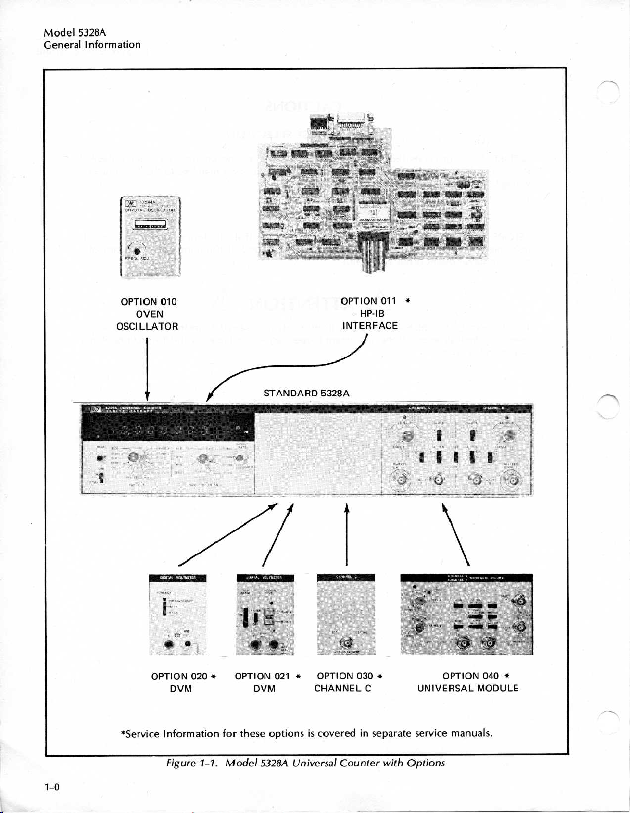
OPTION
OVEN
OSCILLATOR
010
OPTION
HP-113
INTERFACE
011
*Service
OPTION
DVM
Information
Figure
020
*OPTION
1-1.Model
for
021
DVM
optionsiscovered
these
5328A
OPTION
CHANNEL
Universal
030
in
Counter
*
C
separate
with
UNIVERSAL
service
Options
OPTION
manuals
040
MODULE
.
Page 10
1-1.SCOPE
1-2
.This
Counter
option
the
5328A
1-3
.
manual
(including
supplied with
Users
This
manualisdivided
SECTIONIGENERAL
ment
supplied,
SECTION
plesofthe
SECTION
of
assemblies,
Troubleshooting
GENERAL
OF
MANUAL
provides
Option
Manual
accessories
II
THEORY
counterinreference
III
MAINTENANCE
recommended
service
010).A
the
5328A.Operating
.
into
INFORMATION
OF
OPERATION
procedures
SECTION
information
separate
sections
five
available,
block
to
contains
test
and
flowcharts
I
INFORMATION
for
installation
information
containing
coversadescription
and
specifications
covers
and
maintenance
equipment,
Hewlett-Packard
the
and
for
the
the
a
descriptionofthe
schematic
and
performance
included
are
Service
5328A
following
of
.
diagrams
service
in this
General
Model
Manualisprovided
(with
the
counter,
general
of
information
checks
section
5328A
options)iscovered
information
options,
operating
each
assembly
includingalist
and
adjustments
.
Model
information
Universal
for
each
:
equip-
princi-
.
5328A
in
.
SECTION
mation
SECTION
and
section
SECTION
tors.A
identificationisincluded
DESCRIPTION
1-4
.
1-5
.The
interval
time
instrument
1-17.The
zero
blanking.Decimal
selectable
an
attenuator,
output.Rear
external
measured
1-6.INSTRUMENT
IV
REPLACEABLE
ordering
for
V
MANUAL
available
standard
are
5328A
input
frequency
(switch
options.Field
.
SCHEMATIC
VI
descriptionofreference
average,
expanded
provides
channels
trigger
panel
OFF)
parts
.
CHANGES
DIAGRAMS
.
5328A
mainframe
and
ratio.A
(as
showninTable
8-digit(9with
an
point
and
provided
are
selector,
slope
connectors
standard.An
or by
another
IDENTIFICATION
PARTS
provideagate
ARM
providesacomplete
OPTIONS
AND
installation of
contains
designators,
measures
totalize
1-3)byinstalling
Option
unit
readouts
for
time
level
control,
switchonthe
signal
input
contains
Option
frequency,
functionisalso
interval
output,
010
Oven
schematicdiagrams
signal
mnemonics
period,
030)
LED
are
displayed
measurements.Each
ac-dc-coupli?ig,
time base
a
rear
panel
(switch
ON)
listofreplaceable
information
Oscillator
and
and
period
provided.The
the
options
display,
automatically.Two
allows
.
average,
describedinparagraph
display
andanoscilloscope
output
armingbythesignal
and
changes
interval,
and
leading
channel
marker
input
infor-
in this
for
being
parts
on
manual
is
contained
component
printed-circuit
time
capabilitiesofthe
storage,
independent
input
and
an
loca-
card
has
an
1-7
.Hewlett-Packard
whichislocatedonthe
your
serial
prefix
differences
are
covered
missing,
manual
contact
.
of
between
witha"Manual
instrument
this
the
nearest
instruments
panel.The
rear
differs
manualand
Changes"
Hewlett-Packard
havea2-section,
4-digit
from
your
sheet
serial
that
instrument.Instruments having higher
included
Sales
10-character
prefix
listed
on
and
identifies
the
with
this
Service
title
pageofthis
manual.If
Office
number
serial
instrument
listed
(OOOOA00000),
changes.If
manual,
serial
change
the
the
at
the
there
are
prefixes
sheet
is
backofthis
Page 11
Model
General
5328A
Information
1-8
.
APPLICATIONS
1-9
.Specific
general
1-10
make
5328A
to
applications
measurements
1-11
quency
1-12
interval
means
1-13
cations
ments
increased
surements,
Option
application features of
.The
the
5328A
means
512
MHz
.The
measurements,and
.The
measurements)and
that
.The
suchasmechanical
(ballistics),
resolution
040
applications
high
sensitivity,
ideally
that
prescaling
with
Option
.
The
dynamic
tobemade
controlled
optional
the
trigger
standard
sonar
logic
timing
allows
unwanted
informationisprovided
the
5328A
frequency
suited
"arming"
integrating
level
5328A
(to10ns)
measurements,
forawide
techniques
030).Direct
range, input
on
virtually
featureofthe
pulse
amplitude
digital
external
does
not
single-shot resolution
and
electromechanical
ranging,
radio
usefulinapplications
signalstobe
are
describedinthe
range,
are
count
attenuators
any
voltmeters
voltages
need
radar
and
rangeofapplications
not
usedtoachieve
speedisrequired
signal
.
5328Aisuseful
measurements
.
The
hysteresis
resetting
device
ranging
ranging
ignored
which
in
SectionIVof
signal
conditioning
and
trigger
measure
when
the
of
100nsmeets
(relays)
and
navigation.The
such
as
and
optical
would
the
5328A
Users
following
.
The
the
100
in
high-speed
level
in
applications
.
trigger
compensation
slope
switch
timing,
computer/peripheral
ranging.The
otherwise
paragraphs
controls
direct
MHz
range
(seeTable
levels
(critical
feature
changes
the
requirements
timeof
Option
trigger
count
frequency range
totalizingorsystem
Manual.The
.
(see
Table
featureofthe
1-3)
permit
suchasburst
in
most
of
Option
the
polarity
for
appli-
flight
measure-
040
provides
timing
delay
feature
the counter
1-3)
(up
fre-
time
040
.
mea-
of
.
1-14
.Using
be
measured.Applications
timing
1-15
.Full
input
030)
1-16
.The
controlled
interfaced to
withanHPAB
1-17.OPTIONS
1-18
.Several
initial
order,
received
Service
this
manual).Options
otherwisebypart
a
.Option
b
.Option
time
measurements,and
bandwidth,
amplifiersisprovided
5328A
(fully
.
Procedures
Manual
Interface
with
programmed)
HP-I13
cable
options
options
supplied
number
010,
011,
Bus
interval
compatible
averaging,
sensitivity,
Option
.
are
are
installedatthe
for
field
with
907,
908
High
Stability
HP-IB
.
include
integrated
and
for
011
via
instruments,
available
installation
each
option
and
909
listed
in
Interface
time
intervalsasshort
cable length
circuit
signal
conditioningofthe
ratio,
totalizing,
HPAB
Table
Time
Interfaceisabletooutput
the
Hewlett-Packard
calculators,orcomputersbysimply
with
the
factory
of
(except
are
ordered
1-2.The
Base.Oven
.
Allows
as
measurements,
propagation
5328A,aslisted
and
the
an option
for
by
following
5328Atooutput
delay
and
scaling
Interface
instrument
are
Option
option
oscillator
100
ps,
with
resolution to 10 ps
phase
measurement
Channel
measurements
below
describedinthe
010,
Oscillator
numberifpart ofaninitial
options
with
data
and
measurements,
.
A, B
(and
measurement
Bus
(HPAB)
interconnecting
.
If
purchasedaspart
is
ready
for
operation
installation
which
are
available
aging
rate<5x10⁻¹⁰
be
controlled
-
.
.
The
:
C
for
data
is
covered
via
5328A
may
logic
Option
and
be
of
an
when
and
order,
/day
the
HP
is
in
.
c
.
Option
do
d
.Option
externaldovoltage
020,
voltage
021,
Digital
measurements
High
Voltmeter
Performance
measurements
(DVM)
.
DVM.Floating
.
.
Single
ended
high
DVM
for
accuracy
trigger
DVM
level
for
and
trigger
external
level
and
Page 12
Option
e
.
direct
f
.Option
single
ments
impedance
Option
9
.
h
.Option
i
.Option
1-19.EQUIPMENT
1-20
The
.Table
Service
1-1
Kits
030,
ChannelC.
count
.
HighPerformance
040,
shot
time
interval;improvedT.I.averaging
with
delay;T.I.
(1
MSl/50n)
907,
Front
Handle
908,
Rack
Flange
909,
lists
listedinTable1-2
and Handle
Rack
SUPPLIED
equipment
DESCRIPTION
Frequency
A=B
.
Kit
Kit
AND
supplied
are
Table
measurements
Universal
marker
.
(for
Kit
ACCESSORIES
with
described
1-1.Equipment
Module.Sameasstandard
;
instrument
.
the
in
hysteresis
without
AVAILABLE
5328A
and
Section
111
Supplied
General
to
512
MHz;15
;
improvedT.I.accuracy;measure-
compensation;switchable
handles)
Table
1-2
.
mV
5328A
.
lists
accessories
HPPART
rms
sensitivity
but
with10ns
available
NO
Model
information
;
input
.
.
5328A
Rack
Rack
Detachable
HP
Interface
Flange
and Handle
Function
Extender
Kit
DVM
Power
Front
(For
Kit
with
Board,
Cord
7'/2
Table
1-2.Accessories
DESCRIPTION
Bus
Interconnect
Handle
instrument
(Installation
above
Service
Extender
Selector
Kits
Board
and
pin(2required)
18
ft
(231
Kit
without
instructions
kits)
:
Kit
ROM
cm)
long 8120-1348
Available
HP
Cable
handles)
included
Kit
10631A,3ft
10631B,6ft
10631C,
PART
NO
long
(914
mm)
long
(1828
mm)
ft
12
mm)
(3656
5061-0088
5061-0076
5061-0082
05328-82020
05328-82004
05328-62016
.
long
1-21.SPECIFICATIONS
1-22
.Table1-3
lists
detailed
specifications
for
the
5328A
including
all
options
.
Page 13
Model
General
5328A
Information
INPUT
ChannelAand
Sensitivity
25mVrms,
50mVrms,40MHz-10GMHz
Min.pulsewidth:5
Coupling:AcorDc,
Impedance
5052
nominal
Trigger
setting
Trigger
Attenuators
DynamicRange:25mVto
0-40
40-100
Maximum
X10,
(Opt.040)1
Ac
coupled
Opt.040
position5Vrms,
Channel
In
COMAposition,
bedomes1MS2II<65pFfor the
500
k52II<65pFfor
position.5052
ChannelC(option
Sensitivity:15mVrms,5MHz-512
Coupling:do
Trigger
Impedance:5052
Maximum
Input Protection:Fused
(standard
B
:
0-40
Hz-40
20
200
Opt.040)
: 1
MS2II<40pF(switch
with
Level:Variable
with0volt
Slope:independent
X1,
X10,
:
MHz;50mVto
MHz
Input
(dc
X1
:250Vrms.dc-50
X100250Vrms,
X2,
X20250Vrms,
:Vmax=200V(peak+dc)
5052
Input:Common
position
Level:0V,fixed
Input:5Vrms
FREQUENCY
FrequencyA(standard
Range:0-100
Resolution:1
Accuracy:±1
Display:kHz,
FrequencyC(option
Range:5-512
Resolution
Accuracy:±1
Display:kHz,
'Trigger
erroris<0
S/Norbetter
For
any
vaveshape,
(or
MHzto0.1Hzindecade
count
MHz
: 1
MHz
count
MHz
.3%ofone
and
amplitude
trigger
-2xpeak
signal
1
.0025
signal
slopeinV/usec
CHARACTERISTICS
and
option
MHz
(dc
coupled)
MHz
(ac
coupled)
kHz-40
ns,
switch
Opt
preset
MHz
140mVp-p
selectable
.
040)
±2.5volts
over
position
(ac
.
selection of + or -
X100
(X1,
X2,
1Vrmsxattenuator
500mVrmsxattenuator
coupled)
1
.25 x10,Vrms/freq.,50
5Vrms,2.5-100
dc-5
1
.25 x 105V
rms/freq.,5-100
dc-500
.25 x 10°Vrms/freq,0
5Vrms,
sameasdo
than20Hz
25-100
coupled
.
dc-100
Aorseparate,
sensitivity
remains
standard
the
Option
remains
040
nominal
030)
nominal
MEASUREMENTS
and
option
MHz
direct
±timebase
030)
MHz
direct
to 0.1Hzindecade
±timebase
period
equaltosensitivityofcounter
errorisless
noise
voltage
slope
!sec
count
count
for
sinewavesof40
than
for40d8
040)
error
error
S/N
.)
Table
040)
coupled
X20
and
selectable1MS2
times
attenuator
slope
with
Opt.040)
kHz
kHz-2.5MHz
MHz
MHz
kHz
.5-25
MHz
for
for
frequency
MHz
switch
the
selectable
same.Impedance
and
high
impedance
5052
.
MHz
steps
steps
be
.
1-3
5052 with
or
setting
setting for
MHz
MHz
dc-20
greater
.
Specifications
PeriodA(standard
Period
the signalattheAinputisaveraged
periods,N,indicatedbythe
for
Time
Range:100ns-108s(10
Resolution:100nsto1sindecade
Accuracy:+1
Time
The
at
by the
Hz
Range:0.1ns-10s(0
;
Resolution
.
Accuracy
B/A
frequencyatB
installed)tothe
whereNis
PERIOD
and
option
Range:0-10
Resolution:100
(10
insto0.1s
Accuracy:+1
Display:ns,
fts,
MHz
ns
with
count
ms,
to1sindecade
opt.040)
±timebase
s
AverageA(standard
Range:0-10
MHz
Resolution:100nsto
(10nsto .001pswith
Accuracy:±1
count
displayed
no.periods
TIME
INTERVAL
B
IntervalAto
(10
ns to 0.1s
Interval
time
interval
Bisaveraged
resolution
(standard
with
opt.040)
count
±
AverageAtoB(standard
between
over
the
switch
:
no.intervals
(
no,
intervals
±100ns±
:
no.intervals
±10ns±
Ino.intervals
with
opt.040.The
time
interval
averaging
inputiscoherent
Minimum
Minimum
pulsewidth:25 ns (10 ns with
dead
mum
repetition
between
current
time
with the
time:150ns(40 ns
rate of10MHz)
the
preceding
interval's start
RATIO
and
C/A
(standard
for
(or
C
frequencyatAismeasured
Range:A:0-10
selected
B:0-100
C:5-512
Resolution
:1
Accuracy:±1countofB
ofB(or C) (N>1)
ForN=1,add±120nsx
(±
12 ns
x
freq.ofB(or C)
the
by
MHz
MHz
MHz
part
inAxN(orAx
MEASUREMENTS
040)
error±trigger error*
and
option
resolution
.01psin
decade
opt.040)
+timebase
trigger error*
averaged
MEASUREMENTS
and
option
ns-10' s
timebase
number
(N=1to10
a
start
error
signalatA
time
of
7 ) .
.1ns-1s with
±100
ns
averaged
±10
ns
averaged
trigger
error
averaged
trigger
error*
averaged
opt.040
for
thosecases
5328A's
time
interval's
event)
MEASUREMENTS
and
option
040)-The
function
C/A
resolution
(orC)±
freq.ofB(or
with
steps
040)-the
over
the
number
(N=1to10
switch
steps
error
040)
with
opt.040)
steps
option
and
error*
040)
a
stop
±trigger
and
intervals,N,indicated
opt.040)
±
10 ps
± 10 ps with
"
±
4
ins
±timebase
+2ns+timebaseerror
hasa"jittered"
when
the
clock
frequency
opt.040)
with
opt.040and
("dead
time"isthe
stop
event
.
ratioofthe
when
option
N
for
switch
(N=1to10')
N)
trigger
error*
C)
.
040)
Opt
period
of
7 )
.
-
signal
040)
opt
.
error
clock
.)
maxi-
time
and
the
030
is
countsofA
.
Axfreq
of
of
in
.
Page 14
-
DIGITAL
DVM
(option
B
A
and
and
Maximum
Meas
10s(N=101)
1s(N=106)
0
1 s
10
1ms(N=10')
Range
Full
resolution(1sec
measurement
Accuracy
(20 min
Temp.Coefficient
(0to40°C)
Input
Input
Normal
Rejection
Effective
Mode
(1
kQ
Response
(step
Maximum
Trigger
Measurements
020and
external
Time
(N=-10o
ms
(N=
:
range
:
.
warm-up)
Terminals
Impedance
Mode
Ratio
Common
Rejection
unbalance)
input)
Level
VOLTMETER
021)-Trigger
voltages
Sensitivity
(N=)
:
0°)
display
time)
:
:
:
:
:
Ratio
:
Time
:
Input
:
:
0
to
±0
.9999.±9
±99
.5°/c
+
±4mV
±
.05%
±0
Single
10
>60
(50
70
±500
2
mV
resolution
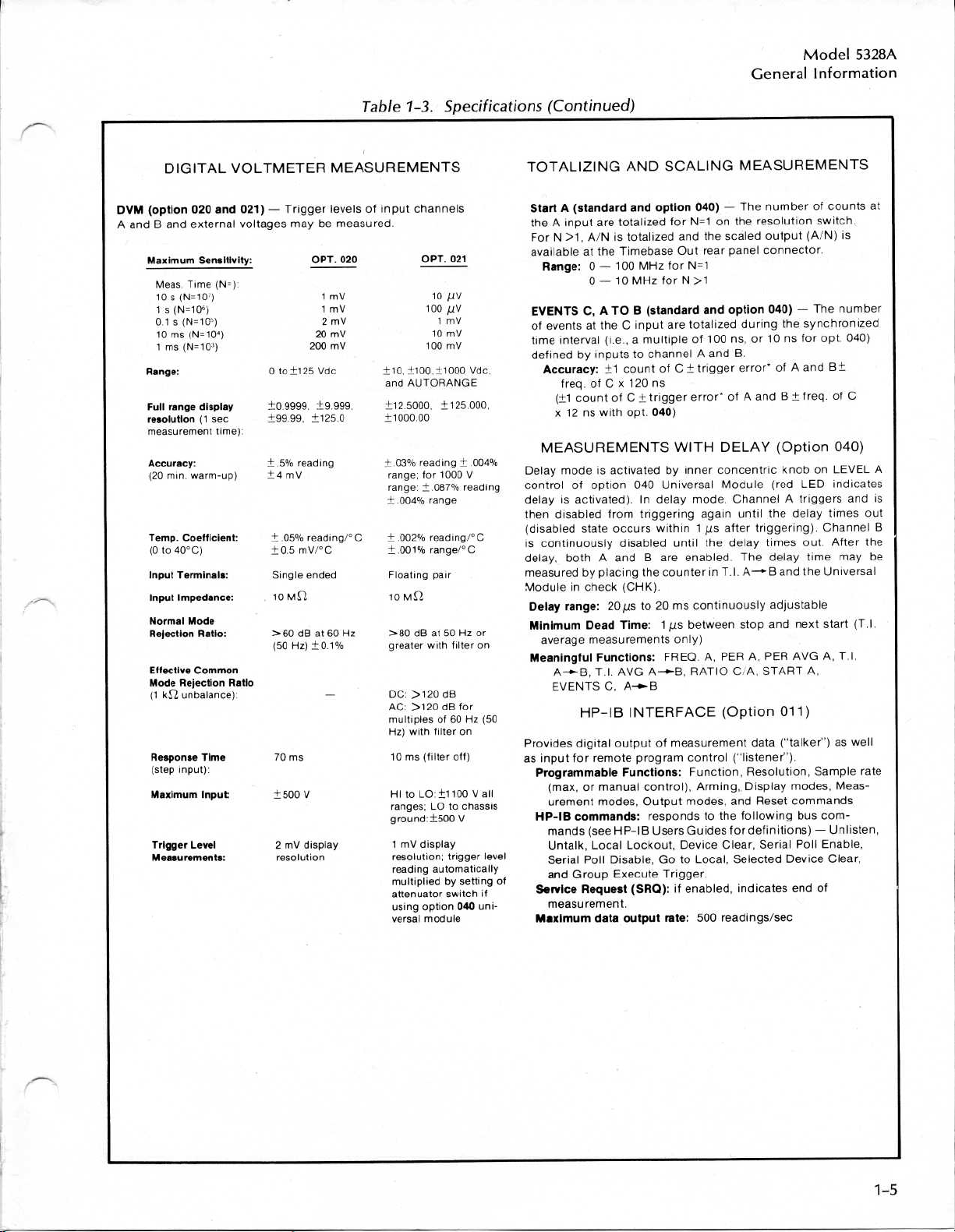
Table
MEASUREMENTS
levelsofinput
maybemeasured
OPT.020
1
mV
1
my
2
mV
20
mV
200
mV
+125
Vdc
.999,
±125
.99,
.5
MSZ
ms
.0
reading
reading/°C±002%
mV/°C
ended
Hz
dB
at
60
Hz)±0.1%
V
display
1-3.Specifications
channels
.
OPT.021
10 /1V
100
UV
mV
110
mV
100
my
±10,±1o0,41000
and
AUTORANGE
+12
.5000,±125
+1000
.00
+
.03%
reading±004%
range,
range:±
.004% range
±
±
.001%
Floating
10
MS2
>80dBat
greater
DC:>120
AC
:
>120
multiples
Hz)
with
10ms(filter
HI
toLO:±1100Vail
ranges;LOtochassis
ground
1mVdisplay
resolution,
reading
multiplied by
attenuator
using
versal
Vdc,
000
for
1000
V
.087%
reading
reading/°C
range/°C
pair
50 Hz
with
filter
dB
for
dB
of
60
Hz
filter
on
off)
:±500
V
trigger
automatically
setting
switch
option
040
module
.
or
on
(50
level
if
uni-
(Continued)
TOTALIZING
StartA(standard
theAinput
ForN>1,
availableatthe
Range:0
EVENTS
eventsattheCinput
of
time
interval(i.e.,a
definedbyinputs to
Accuracy
freq.of
(+_1
countofC±trigger
12nswith
x
MEASUREMENTS
Delay
mode
controlofoption
delayisactivated).In
then
disabled
(disabled
is
delay,
measuredbyplacing
Moduleincheck
Delayrange:20/is
Minimum
Meaningful
state
continuously
bothAandBare
average
A-B,T.I.AVG
EVENTS
HP-113
Provides
as
of
digital
input
for
Programmable
(max,ormanual
urement
HP-IB
commands:respondstothe
mands
Untalk,
Serial
and
Group
Service
Request
measurement
Maximum
AND
SCALING
and
totalized
totalized
is
Timebase
100
MHz
MHz
multiple of
x
120
opt.040)
option
for
for
for
are
channel
ns
and
Out
N>1
are
A/N
-
0-10
C,ATOB(standard
:±1countofC±trigger
C
WITH
activatedbyinner
is
from
occurs
Dead
measurements
Functions
C,
040
triggering
disabled
the
(CHK)
to20ms
Time
:
A-B,
A-'
B
Universal
delay
within1fts
until
enabled.The
counter
.
1
Fts
only)
:
FRED.A,
INTERFACE
outputofmeasurement
remote
program
Functions:Function,
control),
modes,Outputmodes,
(see
HP-113
Local
Poll
data
Users
Lockout,
Disable,Goto Local,
Execute
(SRO):if
.
output
Device
Trigger
enabled,
rate:500
040)-The
N=1
on
the
scaled
rear
panel
N=1
and
option
totalized
100
ns,
A
andB.
error'ofA
DELAY
concentric
Module
mode,
Channel
again
after
the
delay
in
T.I.
continuously
between
PERA,PER
RATIO
C/A,
(Option
(''listener")
control
Arming,
and
Guides
for
Clear,
.
readings/sec
Model
General
MEASUREMENTS
numberofcounts
the
resolution
during
or 10nsfor
error`ofA
andB±freq.of
(A/N)
output
connector
040)-The
the
synchronized
and
(Option
knobonLEVEL
(red
LED
A
triggers
until
the
delay
triggering).Channel
out.After
times
delay
and
adjustable
and
next
AVG
START
time
the
A,
A-B
stop
011)
data
("talker")
.
Resolution,
Display
modes,
Reset
commands
following
definitions)
Selected
indicates
Serial
bus
Poll
Device
end
5328A
Information
number
B±
is
.
at
.
040)
C
switch
.
opt
040)
A
indicates
and
is
times
out
B
the
may
be
Universal
start(T.I
A,
Sample
com-
-Unlisten,
Enable,
of
T.I.
as
Meas-
Clear,
.
well
rate
Page 15
Model
General
5328A
Information
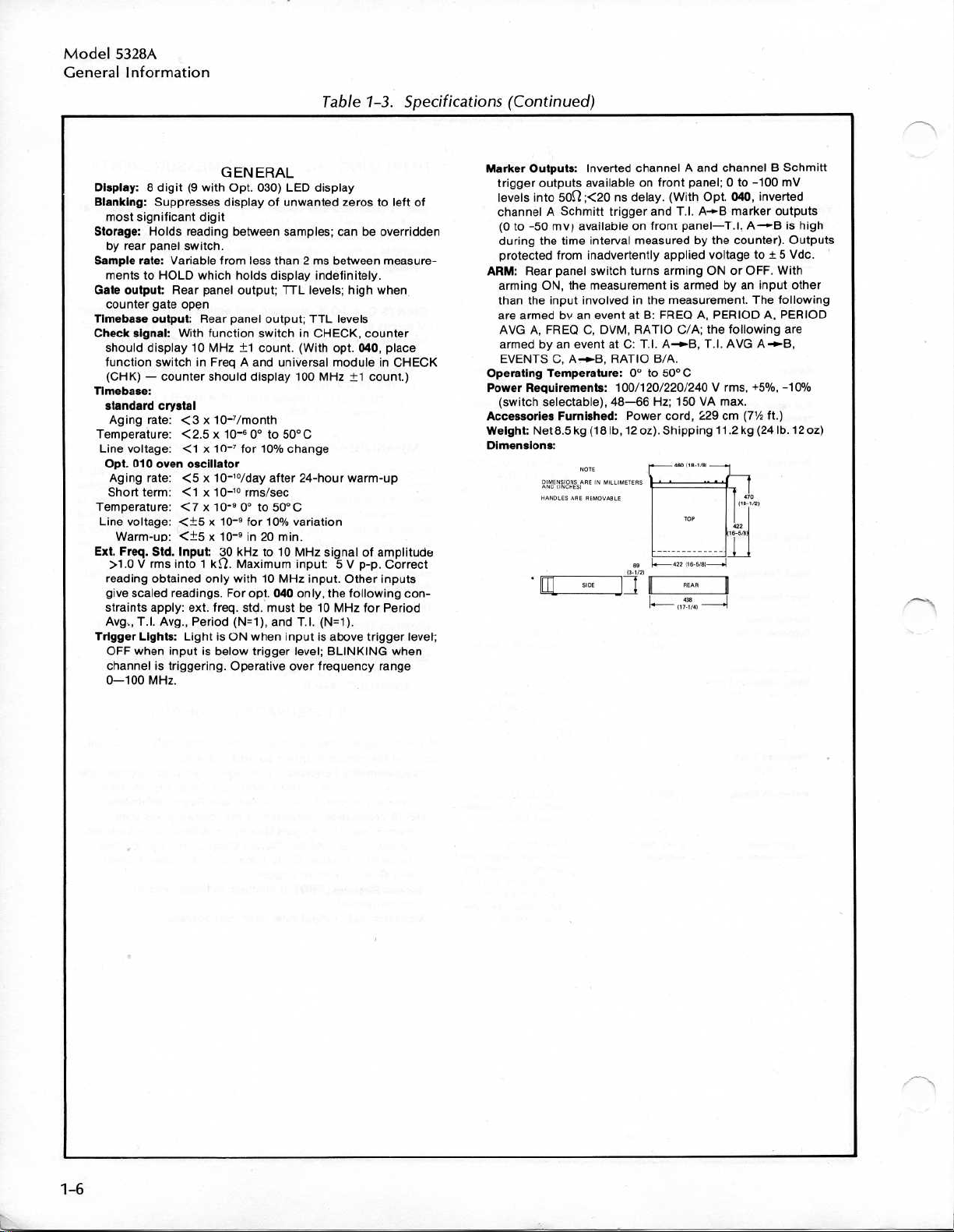
GENERAL
Display:8 digit (9
Blanking:Suppresses
most
significant
Storage:Holds
by
rear
Sample
panel
rate:Variable
mentstoHOLD
Gate output:Rear
counter gate
Tlmebase
Check
signal:With
should
output:Rear
display10MHz
function
(CHK)-counter
Tlmebase
:
standard
Aging
rate
Temperature
Line
voltage
Opt.010 oven
Aging
rate
Short
term
Temperature:<7x10-90°to50°C
Line
voltage:<±5
Warm-up:<*5x10⁻⁹in20min
Ext
.
Freq.Std.Input:30
>1
.0
V rms
reading obtained
give
scaled
straints
apply:ext
Avg.,T
Trigger
.I.Avg.,Period
Lights:LightisON
OFF
when
channelistriggering.Operative
0-100
MHz
with
digit
reading
switch
from
which
panel output;TTL
open
function
switchinFreqAand
should
crystal
:<3x
10-7/month
:<2.5
x 10-600to500
10-
:<1
x
oscillator
:
x10-1
<5
:<1
x
10-1°
x
10
into1kQ.Maximum
only with10MHz
readings.For
.
freq.std.mustbe10
inputisbelow
.
Opt.030)
LED
display
displayofunwanted
between
samples;can be
.
less
than 2msbetween
holds
display
indefinitely
levels;high
panel
output;TTL
switchinCHECK,
±1
count.(With
universal
display
100
C
7
for
10%
change
°/day
after
24-hour
rms/sec
for
-9
10%
variation
.
kHzto10
MHz
input:5 V
input.Other
opt.040
(N=1),
only,
andT.I.(N=1)
when
inputisabove
trigger
level;BLINKING
over frequency range
Table
Specifications
1-3
.
zerostoleft
overridden
measure-
.
when
levels
counter
opt.040,
place
moduleinCHECK
MHz
±1
count
.)
warm-up
signalofamplitude
p-p.Correct
inputs
the following
MHz
for
con-
Period
.
trigger level
when
(Continued)
Marker
Outputs:Inverted
trigger
outputs
levels
of
into
channel
(0to-50
during
protected
ARM:Rear
arming
the
than
are
armed
availableonfront
509
;<20nsdelay.(With
A
Schmitt
mv)
availableonfrom
the
time
from
inadvertently
panel switch
ON,
the
input involvedinthe
by an
AVGA,FREQC,DVM,
an
by
eventatC:T
armed
EVENTSC,A-+B,
Operating
Power
Accessories
Temperature:0°to50°
Requirements:100/120/220/240Vrms,
(switch
selectable),
Furnished:Power
Weight:Net8.5kg
Dimensions
DIMENSIONS
AND
HANDLES
:
IINCHES)
NOTE
AREINMILLIMETERS
ARE
REMOVABLE
;
channelAand channelBSchmitt
panel;0 to
trigger
andT.I.A-B
panel-T.I.
interval
measuredbythe
applied voltageto± 5
turns
armingONor
measurementisarmed
measurement.The
Opt.040,
-100
mV
inverted
marker
outputs
A-B
is
counter).Outputs
Vdc
OFF.With
by an
input
other
following
eventatB:FREQA,PERIODA,PERIOD
RATIO
RATIO
C/A;the
. I .
AFB,T. I.AVGA+B,
B/A
.
following
are
C
+5%,
48-66Hz;
(18
lb,12
cord,
oz).Shipping
Bs
~-<sx
13-,/zl
150VAmax
229cm(7
11 .2kg(24lb.12oz)
(,B-BIBI-
.~
flEAfl
.
1/2ft
-10%
.)
high
.
Page 16
INTRODUCTION
2-1
.
2-2
.This
an
overall
VI.The
Selector,
and
Interface
2-3.OVERALL
2-4
.
standard
section
block
standard
A10
DVM's,
021
is
The
5328Aisa
configuration
"Frequency
"Period-100
"Period
"Time
"
Time
"Totalize
"Ratio
"
Check
contains
diagram
mainframe
Synchronizer,
Option
coveredina
DESCRIPTION
basic
-
100
ns
Average
Interval-100
Interval
-
100
Average
100
MHz/10
THEORY
a
description
in this
section
assemblies
A19
Channel
030
separate
universal
it
offers
MHz
resolution
10
MHz
ns
MHz
MHz
SECTION
of
the
andtoindividual
are the
Attenuator,
Option
C,
manual
counter
following
the
direct
count
F
04
clock
single-shot
OPERATION
OF
operating
A1
and A16
040
for
each
mainframe
universal
~¢
~
resolution
II
principles
block
Motherboard,
Display.Detailed
Universal
option
.
that
counter
schematic
and
A2
Module,
supports
functions
of
the
counter
Power
theory
and Option
diagrams
Supply,
several
:
Theory
in
reference
in
A4
Function
Options
for
011
options.In
Model
Operation
of
to
Section
020
HPAB
its
5328A
2-5
.The
level
trigger
2-6
.Capabilities
voltage
single
isahigh
M11
10
integration
resolution).For
ChannelCOption
protected
requiringaprecision
available
2-7
Option
measurements
inputs
range,
lights
measurements
ended
performance
floating
.
.For
040
"Frequency
"Period-10
"Period
Time
"
"Time
"
Totalize
"Ratio-100
"Check
have
three-position
that
act
can
inputs,
inputs,
time,
and
applications
030isavailable
input,
greater precision
and
is
available.It
.
Its
Average
Interval-10
Interval
-
-
100
matched
attenuators
logic
like
be
greatly
.
Option
125V
range,
unit that
switchable
speed
high
requiring
ninth
-
MHz
base,
has
MHz
100
digit
in
a
ns
the
MHz
a
time
functions are
100
ns resolution
Average
100
MHz/10
MHz
(±4
ns)
100
(x1,
probes,
020isan
0
has10/AV
the
100
:
direct
MHz
single-shot
-
and
expanded
economy
.5%
accuracy,
sensitivity,
filter,0.03%
acquisition
greater
This
option
.
added
high
counter
basic
MHz
clock
count
clock
100
MHz
MHz
amplifiers
00,
x100),
high
speed
selecting
by
version
and
the"read
automatic
accuracy,
(upto300
frequency
offers15mV
eight
to
the
performance
functions,
for
increased
resolution
phase
jittered
withacor
1
Mn
output
options.Two
that
read
readings
range,
sensitivity
mainframe
digit
oven-stabilized
high
resolution
clock
impedance,
input
markers
offers
trigger
or
manual
trigger
a 5
performance
coupling,±2.5V
do
.
DVM
options
millivolt
level"
per
to
across
in
sensitivity,10Mf1
function.Option
range
controlto1000V,
function,
level
second
512
MHz
the
display
.
time base
universal
time
interval
trigger-
controls,
slope
provide
variable
with two-dgit
direct
count
band,
5062
For
applications
Option
010
module
and period
do
021
fuse-
is
Page 17
Model
Theory
J
W
Z
Q
d
F
2
O
5328A
of
Operation
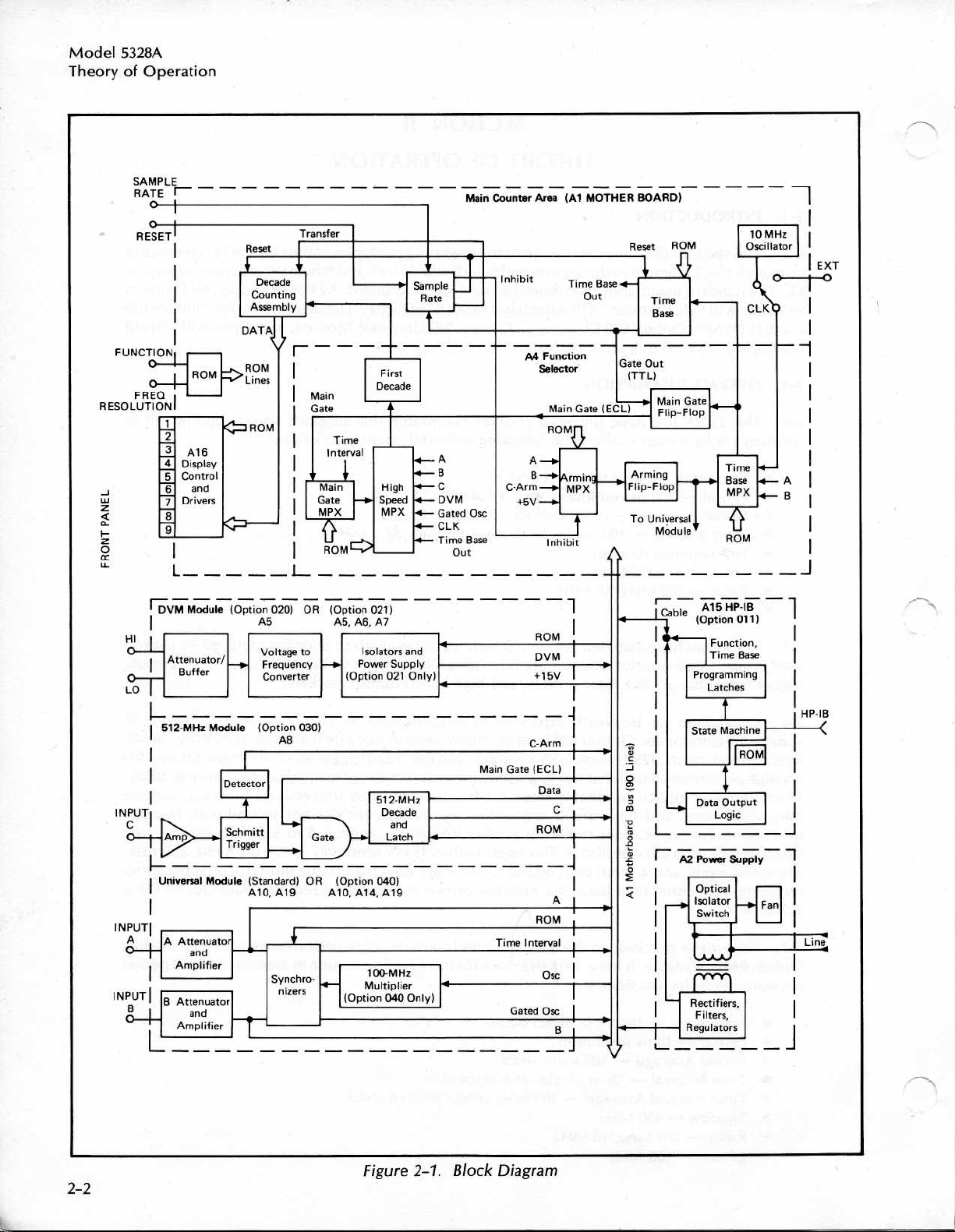
SAMPLE
RATE
r
Main
Counter
Area
(Al
MOTHER
BOARD)
Reset
ROM
INPUTI
C
F
-
D
VM
I
Universal
Module
(Option 020)OR(Option
A5
Module
(Standard)
A10,
A19
A5,
A6,
OR(Option
A10, A14,
021)
A7
040)
A19
ROM
1
Power
ROM
Supply
c
0
I
-
r
0
A2
J
2-2
Figure
2-1
.
Block
Diagram
Page 18
The
2-8
.
three-position
logic-probe
andavariable
2-9
.For
2-10
2-11
2-12
an
internal
2-13
instrument.Its
off
switchofthe
lineisnever
eliminating
ofatriac,
inputs
trigger
systems
Configuration
.
.The
"The
"The
"The
"The
.Each
.
5328Aisorganized
main
input
power
Hewlett-Packard
section
bus
The
power
the
whichisswitched
have
matched
attenuators
channelAhigh
lights,
feature
delay
applications
counter
options
supply
operates
system.The
supply
capacityissufficient
instrument
broken.Unregulated
need
for
time base
(±2
x2,
(x1,
.
Hewlett-Packard
into
section
section
section
Interface
relatively
two-way
provides
operates
off
by an
ns)
amplifiers,
x20),1
Md1or50f1
speed
four
main
Bus
(HP-IB)
independently
bus
consistsof90
regulated
accommodate
to
onlythe
is
constantly
do
warmup.The
optical
ac/dc
switchable
marker,
Interface
operating
option
voltage
do
central
fan
gets
isolator
coupling,
interval
time
Bus
sections
section
and
communicates
lines
.
for
the
any
combinationofoptions
power
fed
its
when
supply
to
the
power
the
±2
input
impedance,
A-to-B
(HPAB)
(refer
other
regulator
oven
from
instrumentisturned
.5V
trigger
high
Option
to Figure
to
the others
operating
;
the
oscillator
ac
power
the
Model
TheoryofOperation
level
range,
slope
control,
speed
marker,
011isavailable
2-1)
:
through
of
sections
.
The
mainacpower
(if
linebyway
the
main
on-
installed),
off
.
5328A
.
2-14
.Main
2-15
.The
standard
containedinthe
BCD
counting
eight
counting
signals
oscillator circuit
internal
2-16
.The
transfer,
the
strobed
accomplished
input
option
2-17
.The
signals
time,
display
interaction
input
the
originator
Counter
main
counter
logic,
decades,
for
the
main
from
signal
sample
andsample
display.Generation
by
modules
Function
A4
through
it
interacts
cycle.The
withthe
option
and
receiver of
Section
counter
with
input
and
the
multiplexerstothe
with
modules.Itisthe
section
the exception
options
latches,
output
The
gate
.
the
input/output
the
optional
rate
circuit
rate
signals
display
is
decoded
Selector
the
display
precision
time
base
module
section
and
multiplexing
oscillator
controls
are
of
control
ECL
assembly
Motherboard
on A1
input
of
.
The
output
section
logictoaccept
crystal
the
generated
decimal
circuits.Data outofthe
and
displayedonthe
servesasthe
decade
control
gate
main
.
main
receiver of
arming
signal
decade
multiplexing
logic,
contains
oven
oscillator
instrument
in this circuit, asisthe
point
and
main
counting
circuitstodetermine
signaliscreatedonthe
The
function
pulses
.
contains
conditioning
counting
logic.The
and
synchronizers
the
standard
external
an
.
display
annunciators
eight-digit
signal
switchofthe
assembly
selector also
the
high
speed
allofthe
and
assembly
decade
and/or
contains
time base
to
room-temperature10MHz
signal
cycle.Inhibit,
BCD
decodingofBCD
and
counting assemblyorthe
LED
instrument.It
the
beginning
the
function
extensive
has
from
data
functional
special
generate
assembly
via
the
reset,
digit
display
timebase
selector
the
logic,
eight
rear
address
.
interaction
modules
subunitsofa
which
decades
contains
precise
panel
main
code
data
routes
At
the
.
and
endofthe
through
and
are
of
timing
or an
gate,
for
are
input
same
with
the
2-18
.The
accept
through
Locatedinthe
code
flexibilityofthe
diverse
the useofa
and
the
data
from
main
counter
three-bit
5328A
various
4K
read-only
time base
comes
combinations
memory
section
code
of
from
the
instrument,
from
the
of
input
(ROM)
the
front-panel
abilityofall
option
as
the
master
the
ROM
switchesorthe
these
operating
modules.This
controlofthe
accepts
the
HPAB
subsections
is
accomplished
instrument
four-bit
remote
to
function
pro-
.
2-
3
Page 19
Model
TheoryofOperation
5328A
gramming
the
instrumenttosetupeach
combinationsofinput
ROMs
user.As
inanupdate
2-19
2-20.The
electronic
handled
2-21.The
speed
the
5328A
twoisthe
fundamental
extends
function,
clock
measurement
2-22
.The
frequency
Schmitt
digit
from
display
ChannelCmoduleisinstalled
board.The
are
plugged
new
each
kit)toacceptit.
.Input
synchronizers
with
from
this
Options
input
environment.They
by
the
universal
is
the
selectionofoneofthe
basic
timing
this
rateto100
the
multiplier
band-limited noisetoprevent
.
middle
capability
trigger
goes
feed
the
module
module,
blank.The
ROM
option
into
the
input
moduleisengineered, the
Section
modules
main
counter
module
for
complex
clock
rate.In
unit.In
MHz
unit,
areaofthe
(ChannelCOption
the 512
onto
ROM
lines
ninth
generates32bitsofoutput
instrument.This
are the
the
MHz
the
deactivate
LED
subsection
modules
main
accept
circuits
contains
timing
the
standard
high-performance
andabasic
upon
command
option
decade.Latchesinthis
data
busand
digitisloaded
.
for
the
are
accommodated
provides
interface
input
signals
.
the
main
measurements.Oneofthe key
two
universal
unit
the
timing
from
the
synchronous
module
the
section
030).A
into
output
the
into
data
which
particular
without
inherent
mainframe
between
and
convert
input
amplifiers,
modules.The
basic10MHz
unit
(Option
unitof10ns.Inthe time
the
ROM,
lockup
provides
5012
fuse-protected
option
display.In
strobing
the
circuitry
mainframe
are
transmitted
measurement
circuit
obsolescence
needs
onlyanew
the
instrument
them
into
the
Schmitt
performance
prime
difference
clock
provides
040),aphase-lock
phase modulates
problems
the
instrument
512
strobe the
functions not requiringaninput
ninth
and
display
throughout
situation.Various
changeasdifferent
protection
ROM
and
proper
triggers,
interval
associated
with
MHz
(least
the
ninth
board
only
amplifier
for
(supplied
the
outside
formtobe
and
high-
options
between
100nsas
multiplier
averaging
the 100
MHz
with
extended
significant)
digitonthe
when
the
of
the
the
this
and
the
2-23
.The
Using a
the
frequency measuring
the
5328A
asanexcellent
unit
(Option
front
disconnects
voltage,
function
of
the
trigger
2-24.The
capability
accuracyof0
increase
through
power
controlled
to-F
converter,aconversion
The
voltmeter
the
Hewlett-Packard
2-25
.This
input
third
areaoftheoption
voltage-to-frequency
with
inexpensive
general-purpose
021),
panel.When
itself
disengages
code
bus
READ
LEVEL
levels
without havingtochange
high
of a
manual
.03%.For
normal
special
supply
terminals,
mode
high
.
Although
voltage
may
technique
the
section
conversion
capabilitiesofthe
accesstothe
single-ended
trigger
from
performance
level
measurementisselectedbymeansofswitches
the
user
selects
the
external
thefunction
and
places0.1s
switch,
measurementisquite
be
the
orautoranging
particularly
rejection
speed
transformers,
noremote
placedinautorange
Interface
resultsina
output
banana
and
gate
instrument
DVM
noisy
to 50dBat
programming
factor of
Bus
(HP-113)
small
frequencyis900x10
contains
technique,
mainframe.The
important
voltmeter.In
either
READ
input
jacks,
timebase
time(1mV
option
floating
10 kHz/voltismaintained
front-panel
returnstoits
and
reset
(021)
DVM
environments, a
50or60Hz.Isolation
optical
easy.Through
and
the
and any
problem.If,
inputs
the
these
capabilityoftrigger
LEVELAor
connects
switches,
sensitivity)onthe timebase bus.Upon
previous
his
function
provides
that
hasarangeof10/.Vto
isolators,
of
the
front-panel
the
user
simply
voltage
for
example,
kHz=9
for
the
optional
modules
low-cost
this
READ
switchable
andanon-board
useofspecial
from
MHz.Inameasurement
providean
unit
level
unit
and
LEVELB,the
itselftothe
places the
state.Thus
and
time base
the
user
filter
for
this
controlsispossible,
regardless of
programs
10,V
the
user puts
digital
(Option
measurementaswell
the
high
locatedonthe
selected
code
the
user
settings
with
the
1000V
may
optionisaccomplished
switching
range
controlsinthe
the
the
DVM
to
1000Vismeasurable
voltmeters
output
900
suited
020)
provides
performance
DVM
trigger
DVM
can
check
.
measurement
andabasic
be
engaged
dc-to-ac
DVM's
function
voltsonthe
time
DVM
module
level
the
on
release
his
remote
V-
range
from
of
.
to
to
.
.
1-
Page 20
second,
to-F
this
converter.To
meaningless
.In
version,
user to
the
compensate
2-26
low-cost
the
attenuator.For
trigger
high
the
three
2-27
levelofone-volt,
performance
need
for
possible
.
Hewlett-Packard
2-28.The
control
cable,
virtually
the counter by
of
the
internally
all
other
providea
would
prevent
data,
thus providing
measurement
with an
example,ifone-volt
DVM,
mental
ranges
fourth
sectionofthe
controlsinthe
front-panel controls.A
moduletobe
the
capabilityofthe
programmed
resolutionof1
the
user
the
trigger
of
importantexception
mentally
x10
combination
in
for
attenuation
multiplication,
of±2.5
volts,±5volts,
Interface
Bus
instrument,
the
HP-1
mounted
HPAB
instrument
special
module
through
option,
HPAB
part
from
misinterpreting
user
withadisplay
levels,
the
.
attenuation
the
the
trigger
is
yields10volts,
with
the
automatically
and ±50
(HP-IB)
B.Plugging
board
controls
with
programming
the
present
see the
5328A
in9x106,far
that
high
performance
Measurement
factor
level
voltage,
and
performance
high
reading
volts
Section
the
HP-113
into
the
assembly
main
function,
the
exception
systemintheHP-I B
system.Foramore
HP-IB
Users
Manual
beyond
his
results,
contains
of
trigger
used
x1
x100
attenuation
out the
.
instrument
time
of
the
.
resolution
the
the
only
performs
DVM
levels
the
universal
in
attenuation
universal
effective
(Option
bus
base, cycle
DVM
and
board
detailed description
limitofthe
module
accurate
much
normally
module
yields
yields
100
module,
trigger
011),
through
rate,
universal
allows
Model
5328A
TheoryofOperation
V-
data
like
the
.
the
blanks
requires
input
effective
an
volts.The
eliminates
level in
provides
the
for
a ribbon
arming,
and
module
any
future
of
2-29.A1
2-30
2-31
2-32
Display
2-33
ROM
display
translated
MOTHERBOARD
.The
A1 Motherboard
a.Display
b
. .
c
.
d
.
e
.
Display
.
.The
control
State
Oscillator
Decade
Time
Base
display
Board
.The
outputsofthe
(A1U37)
and
provide
from
.control
.
Counting
.
Control
control sectiononA1
the
and
.
The
outputsofthe
control
BCD
strobedbyU39.U39
blankingisprovided by
provide outputs
instrument
2-34
.
State
relatedtofunction
.
Control
(Figures
.
.
Assembly
other
circuitsofthe
A16
functions
seven-segment
to
decodes
the
latch
6-5
and
.
Motherboard
counter
Display
ROM
Board
for
position
other
formindecoder
the
digit
address
comprisedofU32B
time
and
consistsoffive
6-6)
.
FUNCTION
the decimal
circuitsofthe
from
code
and
base
codes
sections,
acts asaninterface
and
RESOLUTION
point
and
annunciators
counter.Data
U41
and
sent to
BCD
to1of 10
U40B.Latches
for
use
from
the
form.Leading
U25,
in
other
follows
as
between
:
the
switchesgoto
the
data
U27,
which
and
display
U26,
sectionsofthe
in
bus
A16
the
the
is
is
zero
U31
2-35
.
generates
U1
signal
2-36
.
2-37
.The
The
state
the
and
generates
Oscillator
5328A10MHz
control
digit
the
section
strobe
select
main
oscillator
is
comprisedofcircuits
code
for
the
Reset,
circuit
Transfer,
and
consistsofECL
U1,
U2, U3, U4,
andU5.
display.CircuitU4receives
inhibit
signals
crystal
.
controlled
oscillator
Decade
the
Sample
Counter
and
Y1
Rate
U15,
2-5
Page 21
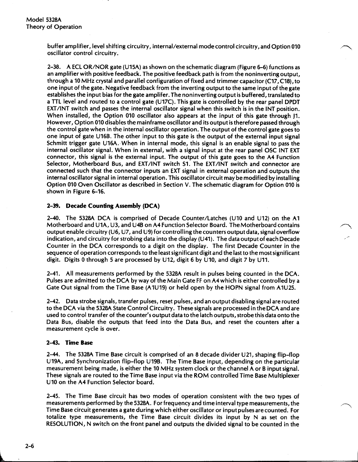
Model
Theory
5328A
of
Operation
amplifier,
buffer
oscillator
2-38
.A
ECL
an
amplifier
througha10
one
input
establishes
a
TTL
level
EXTANT
When
However,
the
one
Schmitt
internal
connector,
Selector,
connected
internal
Option
shown
switch
installed,
control
input
trigger
oscillator
oscillator
010
in
level
control
ofthe
the
Option
of
Motherboard
Figure
circuitry
OR/NOR
with
positive
MHz
crystal
gate.Negative
input
and
routed
and
the
010
gate
wheninthe
gate
U16B.The
gate
signal.When
this
signalisthe
such
that
signal
Oven
Oscillator
6=16
shifting
.
gate
feedback.The
and
bias
for
toacontrol
passes
Option
disables
U16A
.-When
Bus,
the
connector
in
internal
.
the
circuitry,
(U15A)asshown
parallel
feedbackfrom
the
gate amplifer.The
internal
010
the
internal
other inputtothis
in
external
and
as
describedinSectionV.
internal/external
on
positive
configurationoffixed
the
gate
(U17C).This
oscillator
oscillator
mainframe
oscillator
in
external,
EXTANT
inputs
operation.This
also
oscillator
internal
withasignal
input.The
switch S1.The
an EXT
operation.The
mode,
mode
control
the
schematic
feedback
inverting
noninverting
gateiscontrolledbythe
signal
appearsatthe
and
gateisthe
this
outputofthis
signalinexternal
oscillator
The
diagram
pathisfrom
and
trimmer
outputtothe
outputisbuffered,
when
this
inputofthis
its
outputistherefore
outputofthe
outputofthe
signalisan
input
at
gate
EXTANT
circuit
schematic
circuitry,
(Figure
the
noninverting
capacitor
same
switchisin
control
external
enable
the
rear
panel
goestothe
switch
operation
maybe
modified by
diagram
andOption
6-6)
functions
(C17, C18),
inputofthe
translated
rear
panel
the
INT
position
gate
through)1.
passed
gate
input
signaltopass
OSC
A4
Function
and
connector
and
outputs
installing
for
Option
010
output,
gate
DPDT
through
goes
signal
the
INT EXT
are
the
010
as
to
to
.
to
is
2-39.Decade
2-40.The
Motherboard
output enable
indication,
Counterinthe
sequenceofoperation
digit.Digits0through5are
2-41
.All
Pulses
are
Gate
Out
2-42
.Data
to
the
DCA
usedtocontrol
Data
Bus,
measurement
2-43
.Time
2-44
.The
U19A,
measurement
These
U10
and
signals
the
on
CountingAssembly
5328A
and
measurements
admittedtothe
signal
strobe
via
disable
5328A
Synchronization
A4
DCA
and
U1A,
circuitry
circuitry
DCA
correspondstoa
from
the
signals,
the
5328A
transferofthe
the
cycleisover
Base
Time
being
made,iseither
are
routedtothe
Function
(U6,
correspondstothe
outputs
is
U3,
for
performed
DCA
Time
State
Base
Selector
(DCA)
comprised
and
U4BonA4
U7,
and
strobing
processed by U12,
by
Base
transfer
Control
counter's
that
.
circuitiscomprisedofan8decade
flip-flop
Time
of
Decade
Function
U9)
for
controlling
data
into
digitonthe
least
by the
wayofthe
(A1U19)orheld
pulses,
board
reset
Circuitry.These
output
feed
into
U19B.The
the10MHz
Base
input
.
Counter/Latches
Selector
the
the
display
significant
digit 6byU10,
5328A
Main
pulses,
datatothe
the
Time
system
via
(U41).The
display.The
digit
resultinpulses
GateFFonA4whichiseither
open
andanoutput
signals
Data
Base
clockorthe
the
ROM
Board.The
counters
and
by the
are
latch
outputs,
Bus,
and
input,
controlled
(U10
and
Motherboard
output
first
the
and
being
HOPN
processedinthe
divider
depending
channel
data,
data
output
Decade
lasttothe
digit7by
countedinthe
signal
disabling
strobe
reset
the
U21,
Time
A
U12)
on
the
contains
signal
overflow
of
each
Decade
Counterinthe
most
significant
U11
.
controlledbya
from
A1U25
signal
are
routed
DCA
and
this
data
onto
counters
shaping
on
or
B
Base
after
flip-flop
the
particular
input
signal
Multiplexer
DCA
A1
.
.
are
the
a
.
2-45.The
measurementsperformed
Time
totalize
RESOLUTION,
Base
Time
circuit
type
measurements,
N
Base
generatesagateduring
switchonthe
circuit
by the
has
two
5328A.For
the
Time
front
panel
modes
frequency
which
Base
and
of
operation
and
either
oscillatororinput
circuit
outputs
divides
the
consistent
time
interval
its
divided
type
input
signal
with
the
measurements,
pulses are
by
N
to
be
two
types
of
the
counted.For
as
set
on
the
countedinthe
Page 22
Model
TheoryofOperation
5328A
of
DCA.The
ated
made
function
2-46
Time
codes
code
mationinthe
2-47
2-48
and+3.5
sections,
2-49
2-50
the
input
turn
current
voltage.At
until
output
collectorofQ1tofall.This
a result,
negative,
current
field of
overcome
outputs
simultaneously.Regardless
availabletothe
.
.The
.
.The
.+5V
.The
same
lengthofthe
Inputisdetermined
Base
both
of
to
A2
being
turnsonQ3
the
theTime
the
Time
various
POWER
power
volts,dc.
so
only
Supply
+5V
output.When
above
startstobuild
the
output goes
voltage
transistors
except
through
flows
L1 to
go
the
the
A4
Base
Base such
(RESOLUTION,
SUPPLY
supply
The
+5V
the
positive
supplyisa
input
its
-
andQ1.
up
time
same
slightly
startstofall
Q3,
Q5,
for
diode
diode
into
the
offsetatthe
Time
Base
of
Function
gate
time
by
(RESOLUTION,
that
measurement
shown
the
inFigures
and-5.2V
voltage
switching
output
and
hence
The
voltageatthe
through
positive
above
turning
provides
and
Q1
CR3
which
CR3
load.This
input
circuit,
thetypeofmeasurement
generated by
the
regulator
voltageisbelow
L1,
feedback
positive
are
and
goes
of
correspondingtoboth
Selector
Time
N)
circuits
sections
charging
+5V.When
off
turned
clamps
coil
comparator
which
Base
N)
switch
6-7and6-8
that
its
output
collector
is
transistors
feedback
off
the
allowing
L1
until
on
selects
the
Time
code.The
and
FUNCTION
resolution
positions
has
are
essentially
will
provided
described
be
has
greater
its
positive
goes
ofQ1now
the output
the
voltage
Q5,Q3,and
via resistor
and
hard,
voltagetoground.During
the
the
output
U1
and
being
the
Base
5328A
and
.
output
five
the
efficiency
nominal
capacitor
via
resistor
reaches
the
energy
turn
operating
performed,
proper
circuit
scale
voltageatthe
voltage
transistor
and
Mainframe
switches
factor
voltages:+5,-5
sameasare the
.
level,
turningontransistor
goes
high
and
R11
this
causing
Q1
R11toreinforce
which
again
modes,
theseoutputs
signal
and
than
comparator
to
Q1
to
the
scale
ROM
outputs
agree
a linear
(greater
increasing
maintain
point
the
the
collectorofQ1
this
partofthe
has
been
goes
on
again
with the
are
gener-
perform
factor
the
.2,+15,-15,
+15V
regulator
U1
Q5which
than
the output
the
comparator
voltageatthe
thecharge
storedinthe
low
of
reads
proper
infor-
and
-15V
its
sees
17V)
situation
goes
cycle,
enough
.
the
and
.
are
the
the
of
+
in
As
to
.The
2-51
sistorQ9provides
2-52
.The+3.5V
U5
being used
protect
2-53
.
2-54
shown
(from
DCA.Inaddition,
of
the
2-55
2-56
to
the
+15V
as a
against
A4FUNCTION
.TheA4Function
in
the
DCA
.High
.High
1st
shorts
Figures
modules
areontheA4Function
Speed
speed
decadeofthe
supplyisa
level
supply
comparatorand
6-9
that
the
Multiplexer,
multiplexer
shifting
is
alsoasimple
.
SELECTOR
Selector
and
6-10.It
process
Main
Refer
DCA:A,
simple
Gate
linear
and
current
servesasthe
receives
the
signal
FF,
the
Selector
Table
to
Main
servesasthe
U6
GATED
B,
regulator
gain
regulator
linear
block.Resistor
gain
main
high-speed
input)
Arming
assembly
NOTE
6-1
for
definitions
and
Gate,
OSC
transistorQ7as
using
while
U3
with
high-speed
differential
and
routes
Multiplexer
.
1st
Decade
main
multiplexer
(GOSC),
the
is
usedascomparator
the
operational
provides
R32
that
data
and
of
mnemonics
DVM,
C,
switching
Arming
and
overcurrent
data
ECL
to either
FF,
.
routes the
TIME
pass
transistor
gain
and
amplifier
limiting
moduleofthe
from
the
theTime
and
BASE
Baseorthe
the
First
following
OUT
(TBO),
.
Tran-
block
section
5328A
Main
Decade
signals
of
to
Bus
and
as
.
7
2-
Page 23
Model
TheoryofOperation
5328A
OSCILLATOR
(enable) of
FF
(LMGF),or(LTOTOLST),
(LTOT"LST),
or
LMGF
the
stretch
light
lines
2-57
isanECL
translatorU2.
decade
theA1
2-58
2-59
or
action
or
enablesU4comes
remaining
ARM
the
respectively.CapacitorsC4.andC5and
elementstoenable
and
A4
Function
any
one-shot (Q6,
MG
and
.The
U3(9), U4(9), U3(5),
Motherboard
.Arming
.TheArming
disabling
occurs
switch.U5
Arming
ROM
(OSC)
.
the
multiplexer
respectively
lock
openMain
SelectorbyECL-to-TTL
ECL
gate
U36B,E)can see
MG
to
outputofthe
High-Speed
The
TTL outputofU2(13) clocks
where
Multiplexer
FF,
Time
Base
via
the
address
signal.TheAandBsignals
line
thus
the
lines IA,
servesasthe
signal
control
Gate
signal
present
operate the
main
binary
and
they
andArming
the
second
Multiplexer
High
Disables
from
Arming
(pin9)is
selects
either
narrow
operating
the
U6(2)
at
remote
multiplexer
the
output
U2(13)
are
latched
halfofU4,
Synchronizers
Multiplexer U5(6).ROM
controlled
C-ARM,
ECL
pulsesonlines;KandBtobeseen by
IB,
andICcontrol
Main
Gate.The
throughU8and
Main
Gate.In
through
translator
U2(10)
the
U10
so that
pulses
Main
U6(15)
of
which
SchottkyquinaryU4andU3.
travel
off
and
FF
servestoinhibit
and
the
by the
A,
derived
are
resistors
the
active
addressofthe
LowTimelnterval
enabledbyROM
addition,
U8C.Main
U2D.Capacitor
the
and
properly
GateofchannelC.
feeds
couples
theA4Function
the
carry
synchronizersinthe
(HDS)
Low
B, or free
from
R17
ROM
Gate
slower
into
feeds
signal
Arm(LARM)
and R18
TTL
react
first
binaryU1of
to pins 14
into
various
from
lines
run
(+5V)asthe
ECL-to-TTL
serveaspulse
multiplexer.Pin
(LTIF),
lines
line
HOPN
statusisdetected
C11 and
control
.
U8D
Selector
the
next
measurements
Universal
U4(6).The
control
signal
translator
can
resistor
chip
differentially
the
main
and
15ofECL-to-TTL
The
outputs
boardtothe
decadeofthe
signal
U5(10,11)
from
signaltosendtoU4
stretcher
theTTL
ArmingFFU4
Low
Main
Gate
LMGF,
override
and
R35
A1U4
by
Module.This
the
U2A
LTIF,
LTIF
sent
off
serve
and
gate
drives
bus
DCA.U1A
of thefirst
DCA
on
DCA
enabling
which
sets
while
the
rear
panel
and
U2B,
timing
2
to
.
as
.
2-60
.Time
2-61
.
signal
resynchronizing
Time
Base
disable
2-62
.U1Bisa
MultiplexerU8and
signal
Synchronizeronthe
levelsatU1(10).The
capacitor
U1(14)
2-63
.An
2-64
.To
of
the
2-65
.Assume
High
Reset
Decade
chiponthe
plexer
pins9,10,
turningontransistorQ1which
Base
Time
Base
via
pin
8tothe
signal
Input
signal.The
U10
.
high-speed
(GATE
.
measurement
U5.Assuming
OUT)
C16
clocks
Example
show
Time
(HRD)
Motherboard
and11of
how
the counterisin
Base
has
Multiplexer
Multiplexer
Time
.
ROM
HDS
ECLFFusedtogenerate
the
remote
is
generated
Motherboard.Resistors
outputofTime
U1(11)
of
Operation
the
above
of
frequencyAis
(HRTB)
momentarily
releases
that
self
U5.When
and
Main
Gate
FF
U10
selects
Base.This
lines
R(HTBA),
signaltoU10(13)orROM
gateinthe
in
yieldingasynchronized
mentioned
the
has
momentarily
gone
LINH
arm
has
the
firstApulse occurs
in
turn
eitherA,B,orOSC
signal
same
R(HTBO),
FrequencyCmodule.A
the
Time
Base
and
R14
Base
Multiplexer
function
giveninthe
middleofits
gone
high
resetting
togohigh.U9(13)
been
selected,Awill
pulls
LINH
low
is
also
and
precise
and
R43B
fast rise
selector
following
display
high
First
U4(4)
again
to
send
the
sent to
R(HTBB)
line
stable
senttoU1
translate
U10
circuits
cycle.Low
resettingU1and
Decade
have
goes
and
U1, the
control
LTOTtoU10(1)
gate
TTL
via
this
via
resistors
and
fall
time
operate
paragraphs
Inhibit
U1, U4,
goes
low
enabling
been
selectedbythe
low
settingU4.
inhibits
Time
Base
Input
Main
Gate
the
selectionofthe
servetoenableor
times
for
the
Main
replicaofthe
the
TTL
signal
R42 and
Main
togetheranexample
.
(LINH)
U4
andU3.
another
Main
line
Main
downtoECL
R43D
Gate
is
and
High
The
Arming
U4(5)
measurement
FF, as
signal
TTL
Reset
control
Multi-
ROM
goes
(TBI)
a
Gate
Gate
Gate
and
on
low,
on
high
2-8
Page 24
from
starting
signalonpin2of
lator
signalonMain
U10(11)
U6(2)
lines
2-66
Gate
U2(10)
Control
2-67
2-68.This
Amplifier
B
Schmitt
period
only
gets
opening
R22,
23,
After
.
Synchronizer
detects
section
STANDARD
.
assembly
channels
trigger,
type
channelAwill
until
Reset
has
U10to
Synchronizer
Gate
clocked causing
the
Main
Gate
and24thus
appropriate
the
signal
closingofthe
the
the
of
module,
with
signal
measurements
A1 Motherboard
TIME
shown
and
A10
conditioning
trigger
discussed
be
occurred
sent into
be
U1(14)
and
A
each
gate
goes
low
INTERVAL
in
Synchronizer
and
lights
For
mostofthe
.
.Ina
frequency
theTime
drives
U1(10)
togolow.This
initiating
event
time
and
Main
block
(SLOPE,
markers,
.
the
counted
is
elapsed(Nclock
has
next
the
Gate
which
MODULE
form
assembly
Base.Shortly
high.On
low
.
count
into
Oscillator
and
sendsaTTL
initiates
AND
(A10
Figure
in
.
These
AC/DC,
synchronizing
and
circuitry,
measurement,
next
the
signal
propagates
SignalAhas
1st
decade
counts
signal
new
a
A19)
6-11,iscomprised
assemblies
ATTEN,
channelAandBare
SEP/COM
theTime
after
Oscillator
been
into
clocks
signal
display
circuitry
the
selectedonU6byROM
U1A, U4A,
the
Main
(LMGF)
cycle
contain
Theory
selects
ROM
Base
signal
through
Time
GateFFU1
toU4in
.
of
A19
the
A)
controls,
time
for
identical.Therefore,
theOscil-
returns,
(through
U8(B
andC)to
andU3.
Base)
the
the
Attenuator/
100
MHzAand
amplifiers,
interval
closed
Model
of
high
a
U10)
Main
State
and
5328A
Operation
.
2-69
.The
position
contacts.It
attenuation
Q1Aand
signal at
The
ResistorR3is
and
capacitorsC4and
Q1
and
2-70
.The
either
.The
2-71
enters
between
output
drives
peak-to-peak
2-72
waveform
position),
does
negative
of
B
successive
the
the
±2
whenever
both
.The
not
invert
edge,
A
switchS3is
B
dual
that
U2B
input
signal
enters
eitheraccoupled
enters the3position
then
node
through
and
resistors
the
node
used
to adjust
circuitsto±3.6volts
SEP/COM
channel
signal
then
Schmitt
generated
.5V
the
theAtrigger
hysteresis
exclusiveORgate
is
desired.When
actsasan
the
and
switchS4to
R3, R4, R6,
between
formanovervoltage
C5
A
switch
attenuator
passes
triggerU1.
by
input
crosses
output
at
inverter
signal
passing
therefore
A19
the
resistorsR6and
any
initial
(S5)
output or theAchannel
through
R1, R2,
and
its
input
U2Bisused
pin5on
.
When
passes
board
through
attenuator
the
FET
andR7connected
voltage.Diodes
offset
(max)
connects
)5(6)
Trigger
and
this
the
.
throughit.
only
the
to
U1
R3 on
reference
exclusive
in
conjunction
U2Bisheld
pin5goes
trigger
(Figure
capacitor
(X1,
impedance
inazero
follows
R7
protection
.
input
of
the
A10
Synchronizer board
compares
its
other
voltage
OR
low
Circuit
events
throughJ2and depending
6-12)
ordocoupled
C7
X100)
X10,
converter
offset
closely
CR2
network
theBchannel
attenuator
the
signal
input
.
The
outputisECL(--
gate
U2B.U1
with
U3
an
ECL
to
(SLOPE
U3
that
switch
isaone-shot
occuronthe
and
stage.This
totem-poll
the
and
limit
to
output
at
(pin
11)
to
select
high
across
passes
signalatthe
resistors
CR3,
the
impedance
(Figure
pin12toado
and
has
approximately15mV
the
level
movedto-
that
slope
the
from
stage
configuration
gateofQlA
signaltotransistor
converter
.
6-13),
changes
to -1
.8V
slopeofthe
(SLOPE
position),
only
triggersona
selectedbyU2B
on
the
the switch
selected
consists
R8, R9,
switchin+
R10
where
reference
at
state
.6V)
and
input
U2B
of
.
.
to
it
its
.
2-73
.The
nanoseconds
U4, an
the
2-74
trigger
long
do
ECL-to=TTL
nanosecond
5
A
similar
.
light
enough
coupledtothe
outputofU3D
width
signal.A
duration
These
.
converter
ECL
pulse
tobeseen
Schmitt
pulseatpin
stretcher
larger
at
pins9and
pulsesgoto
and
pulse
is
usedtoconvertthe
feedback
when
trigger,
itfunctions
are
15
the
A4
stretcher.The
10 to
an approximately
capacitor
driving
like a
differential
Function
tigger
(C20)isusedtoconvertthe
the
trigger
logic
ECL
Selectortobe
feedback
light
probewith
through
nanosecondn'L
25
outputatSchmitt
LED.Because
pulses of
adjustable
approximately
countedasA
capacitor
pulse
trigger
outputtoa
this
pulse
threshold
events
C16
stretches
pin12.
at
U1(15)toa
pulse
stretcher
voltage
5-10
and
to
of
is
.
2-
9
Page 25
Model
TheoryofOperation
5328A
When
thechannel
inputislower,
the
blinksonor
2-75
.The
generate
AVE,
PER
(HDS)
ECL
high,
low
_U5C
TI
goes
output 10
and
selects
measurements)
low.This disablesTIand50-SCsending
U7(6)
gatestoreset
2-76
.U7(8)isa
event
2-77.A16
2-78
.The
in
additontoswitchesS1(POWER),
SAMPLE
off
remaining
synchronized
and
line,
the RS
and
and
pin12on
low,
telling
MHz
channelAas
has
been
DISPLAY
Display
RATE
inputishigher
A
the
LEDisOFF,
depending
circuitry
time
PER
AVE
functions.Afterareset
FF's
(U5)
GOSC
all
isatVBB--1
U7
theA4
oscillator
theFFoutput
FF's
and
control
detected
controlR6as
line
ASSEMBLY
Assembly
on
interval
andDFF's
high.The
Function
pulses.Whenastop
the
stop
atU5(3
thus
which
.
contains
shown
than
the
trigger
and
wheneveritpasses
the
polarityofthe
consisting primarilyofIC's
and
gated
(U7)
are
.2V.Whenastart
next10MHz
Selector
event
)
prepare
disables
S2
in
that
for
PERIOD
goes
high,
them
the
the
display,asshowninthe
(RESET),S3(FUNCTION),
the
schematic
level
input
oscillator
pulse
entersonthe
reset
through
event
clock pulse
thetime
event
occurs
measurements
and
synchronoustothe
them
high
for
the
stop
channelinPeriod
setting
pulses
interval
again,
next
diagraminFigure
the
trigger
through
signal
U6B
enters
measurement
the
.
U5, U6, U7, U9,
for
the
High
andTIisanECL
U5(13),itsets
synchronously
has
at
U5(1),
andBas
then propogates
block
S4
(FREQ
light
LEDisON.When
trigger
begun.GOSC
(U9isa2input multiplexer
measurements
threshold,
and
U10isused
mainframetouse
Disables
next
.
diagraminFigure
RESOLUTION,
6-15
Sny
high,
theFFoutput
setsU7(9)
also
the
stop
oscillator
through
.
chron
GOSC
event
untilastart
the
inTI,TI
high,
begins
for
pulse
two
6-14,
N)
LED
izers
is
and
sets
and
to
an
at
to
TI
U6
2-79
.The
seven-segment
units
digits
2-80
.The
through
transistors
from
display
(DS10-DS16)
and
annunciators
digit
Q9tostrobe
Q13-Q20
the
Motherboard
consistsofa
LED
numeric
in
additiontooverflow
are
automatically
address
each
.
The
through
code
digit
gate
9-digit
display
from
which
(DS19),
transistors
(9th
(DS1-DS9)
(DS17),
displayed
A1U39
on
receives
remote
Q10,
digit
and
the
the
(DS18),
Q11,
with
used
annunciators
remote
(DS18),
with
the
correct
Motherboard
seven-segment
and
overflow
and
Q12,
Option
030,
for
indicating
and
gate
decimal
is
appliedtotransistors
code
(DS17)
respectively
FrequencyConly)
measurement
(DS19).The
point
from
A1U41
LED's
receive
.
display
.
through
signals
Q1
Page 26
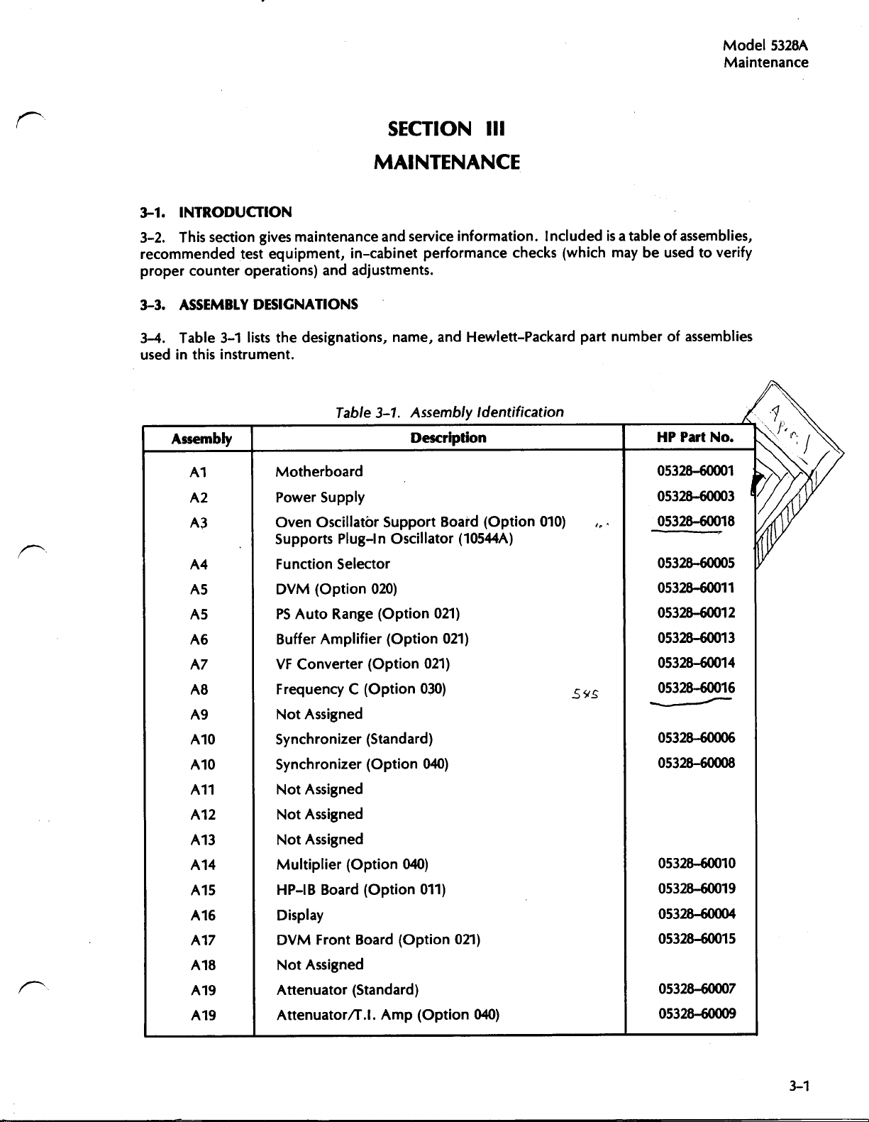
Model
Maintenance
5328A
INTRODUCTION
3-1
.
3-2
.This
recommended
proper
3-3
3-4
used
counter
ASSEMBLY
.
.Table
in
this
Assembly
A1 Motherboard
A2
A3
A4
AS
A5
A6
A7
A8
A9
A10
A10
section
test
operations)
DESIGNATIONS
lists
3-1
instrument
.
maintenance
gives
equipment,
designations,
the
.
Power
Oven
Supports
Function
DVM
Auto
PS
Buffer
Converter
VF
FrequencyC(Option
Not
Assigned
Synchronizer
Synchronizer (Option
in-cabinet
and
adjustments
Table
Supply
Oscillator
Plug-In
Selector
(Option
Range
Amplifier
(Option
(Standard)
SECTION
MAINTENANCE
and
service
name,
.
Assembly
3-1
Description
Support
Oscillator
020)
(Option
(Option
information.Includedisa
performance
.
and
Board
021)
021)
021)
030)
040)
III
checks (which
Hewlett-Packard
identification
(Option
(10544A)
010)
part
Svs
,,
table
may
number
of assemblies,
be
used
to
of
assemblies
HP
PartNo.
05328-60001
05328-60003
05328-60018
-'
05328-60005
05328-60011
05328-60012
05328-60013
05328-60014
05328-60016
05328-60006
05328-60008
verify
A11
A12
A13
A14
A15
A16
A17
A18
A19
A19
Not
Assigned
Not
Assigned
Not
Assigned
Multiplier
HP-IB
Display
DVM
Not
Attenuator
Attenuator/T
(Option
Board
Front
Assigned
040)
(Option
Board
(Option
(Standard)
.I .
Amp
011)
021)
(Option
040)
05328-60010
05328-60019
05328-60004
05328-60015
05328-60007
05328-60009
Page 27
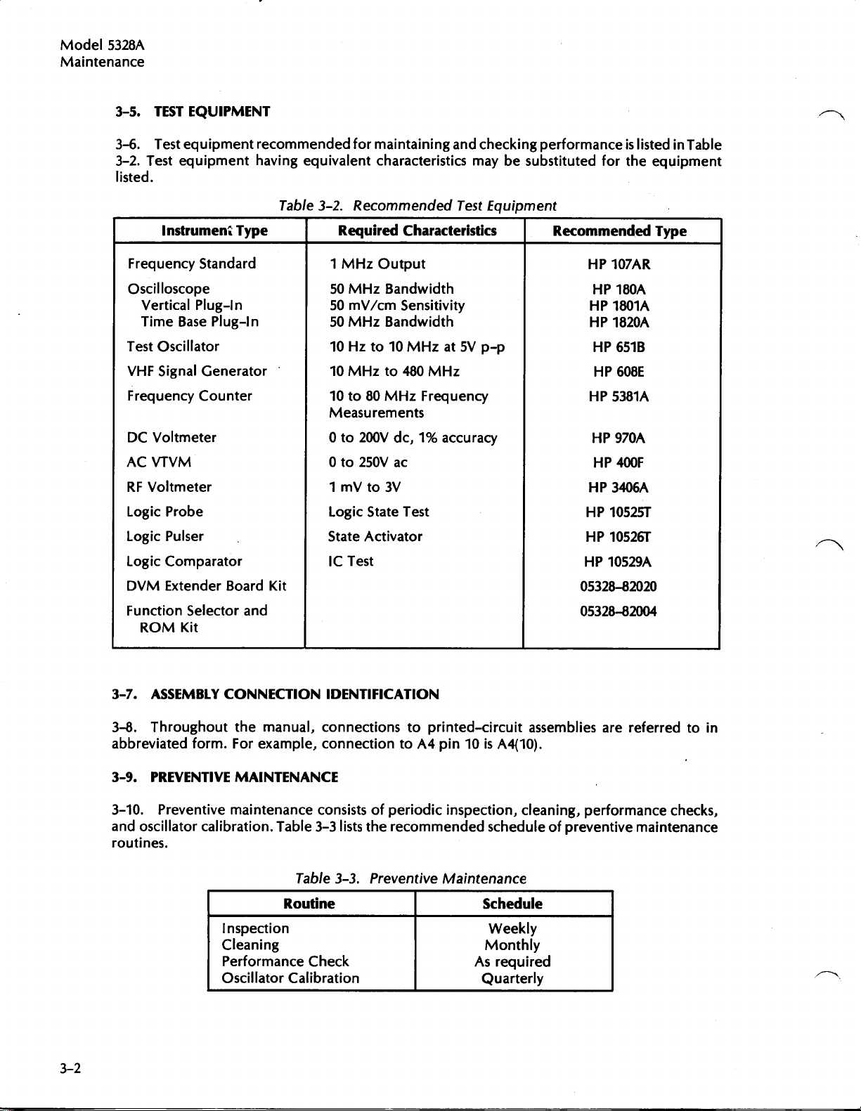
Model
Maintenance
5328A
3-5.TEST
3-6
.Test
3-2.Test
listed
.
Instrument
Frequency
Oscilloscope
Vertical
Time
Test
Oscillator
Signal
VHF
Frequency
DC
Voltmeter
VTVM
AC
RF Voltmeter
Logic
Probe
Logic
Pulser
Logic
Comparator
DVM
Extender
Function
ROM
EQUIPMENT
equipment
equipment
Standard
Plug-In
Base
Plug-In
Generator
Counter
Board
Selector
Kit
recommended
having equivalent
Table
3-2
Type
Kit
and
for
maintaining
characteristics
.
Recommended
Required
1
MHz
50
MHz
50
mV/cm
50
MHz
10Hzto10MHz
10
MHz
10to80
Measurements
0to200V
0
to
250V
1
mV
Logic
State
IC
Test
Characteristics
Output
Bandwidth
Sensitivity
Bandwidth
to
480
MHz
dc,
ac
to
3V
State
Test
Activator
and
Test
at5Vp-p
MHz
Frequency
1%
accuracy
checking
may
be
Equipment
performance
substituted
Recommended
HP
HP
HP
HP
HP
HP
HP
HP
05328-82020
05328-82004
for
HP
HP
HP
HP
HP
is
listedinTable
the
equipment
107AR
180A
1801A
1820A
651B
608E
5381A
970A
400F
3406A
10525T
10526T
10529A
Type
3-7.ASSEMBLY
3-8.Throughout
abbreviated
3-9.PREVENTIVE
3-10
.Preventive
and
oscillator
routines
form.For
calibration.Table
.
CONNECTION
the
manual,
example, connectiontoA4
MAINTENANCE
maintenance
Routine
Inspection
Cleaning
Performance
Oscillator
IDENTIFICATION
connections
consistsofperiodic
3-3
lists
Table
3-3.Preventive
Check
Calibration
to
the
recommended
printed-circuit
pin10is
inspection,
A4(10)
cleaning,
scheduleofpreventive
Maintenance
Schedule
Weekly
Monthly
As
required
Quarterly
assemblies
.
performance
are
referred
to
checks,
maintenance
in
Page 28
.
3-11
3-12.The
Electronic
signs
Inspection
5328A
components
of deterioration
shouldbemade
wear,
looseness,
3-13
.
Cleaning
3-14
.The
ensure
cleaning
instrument
trouble-free
compound
should be
that
shown
shouldbechecked
verify
to
proper
misalignment,
should
operation.A
may
be
100/120/220/240
EITHER
CAUTION
TOP
OR
DURING
REPAIR.AVOID
POWER
BEFORE
ASSEMBLIES,
inspected
for
indicationsofmechanical
signsofoverheating,
andathorough
operation.Mechanical
corrosion,
be
kept
dry
used
.
free of
clean
and
cloth,
WARNING
VAC
SUPPLY
BOTTOM
COVER
TROUBLESHOOTING,
DAMAGE
TO
REMOVING
OR
COMPONENTS
other
signs
dust,
moisture,
bristled
a soft
WIRES
IS
REMOVED
ARE
INSTRUMENT
OR
REPLACINGCOVERS,
.
and
leakage,
frayed
investigationofthe
parts
shouldbeinspected
of deterioration
grease,
and
brush,ora
EXPOSED
.
USE
WHEN
EXTREME
ADJUSTMENT,
BY
REMOVING
electrical
insulation,
and
associated
for
excessive
.
foreign
matter
cloth saturated
OR
Model
Maintenance
defects
.
other
circuitry
to
with
5328A
3-15
.
In-Cabinet
3-16
.GENERAL
can
used
usedtoverify
be
:
a
.As
Periodically, for
b
.
c
.As
d
.After
e
.Asapermanent
pages
3-17
.
REPAIR
3-18
.
Printed
3-19
.Component
electrical
plating
3-20
contact
and
.
Replacing
Performance
.The
partofan
partofa
any
repairsoradjustments
are
perforated
Circuit
between
the
replacement
Integrated
Check
performance
and
record
incoming
proper
inspection
instruments
procedure
to locate
recordofinstrument
and
may
Component
lead
holesinthe
Replacement
conductorsonopposite
component,
Circuits
check
(Table
3-4)
operationofall
checkofinstrument
usedinsystems
defective
and
before
maintenance
be
removed
circuit
boards
sidesofthe
apply
heat
and
test
card
circuitsofthecounter
specifications
where
circuits
returning
maximum
.
instrumenttoregular
performed, because
.
have
plated-through
board.To
sparingly,
and
sheet
that
follows
and
may
.
reliabilityisimportant
the
wallstoensure
prevent
work
damagetothe
carefully
.
the
service
test
check
also
record
good
be
.
.
3-21
.Following
a.SOLDER
b
.CLIP-OUT
soldering
the base
wires
from
are
two
GOBBLER
iron
with
.This
recommended
.
Thisisthe
hollow
a
method
methods
best
tip
connected
shouldbeused
as possible.Withasoldering
each hole.Then
clean
the
of
replacing
integrated
method.Solderisremoved
as a
iron
holes
toavacuum
last
resort
and
long
.
source
only.Clip
nose
pliers,
circuits
from
.
the
leads
carefully
:
board by
close
as
remove
a
to
the
Page 29
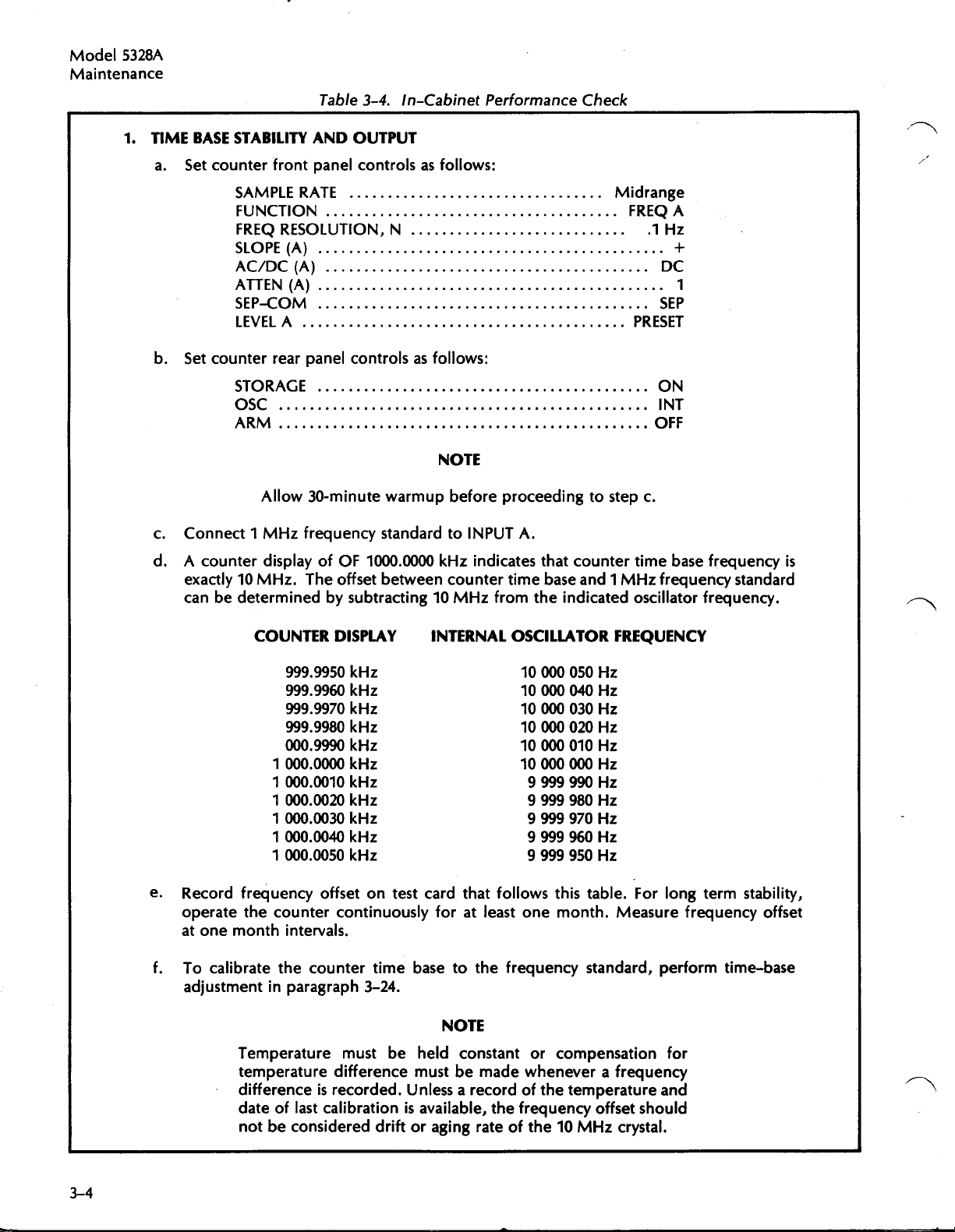
Model
Maintenance
5328A
Table
3-4.In-Cabinet
Performance
Check
1.TIME
BASE
a
.Set
b
.Set
c
.Connect1MHz
d
.A
exactly10MHz.The
canbedetermined
STABILITY
counter
SAMPLE
FUNCTION
FREQRESOLUTION,N
SLOPE
AC/DC
ATTEN
SEP-COM
LEVELA. . . . .
counter
STORAGE
OSC
ARM
Allow
counter
displayofOF
AND
front
panel
RATE
(A)
(A)
(A)
rear
panel
. . .
. ... . . . . . . . . . . . . . . . ... .
. .
. . . . . . . . . . . . . . . . . . . .
30-minute
frequency
OUTPUT
controlsasfollows
. . . . .
. . . . . . . . . . . . . . . . . . . .
. . . ... .
. .
. . . ... .
. . .
. . .
.
. . . . . . . . . . . . . . . . ... . . .
by
. . . . . . . . . . . . . . . . . . . . ... . . .
. . . . . . . . . . . . . . . . .
. .....
.
. . . ... . . . . . . ..... . . ...
. . . . . . . . . . . . . . . . . . . . .
. . . . . . . . . . . . . . . . . . . .
. . . . . . . . . . . . . . . . . . . .
. . . . . . . . . . . . . . . . . . . .
controls
warmup
standardtoINPUTA.
1000
offset
between
subtracting10MHz
as
.0000
follows
. .
. . .
NOTE
before
kHz
counter
:
. .
. .
. .
. .
. . .
. . ... . . . . . . ... .
. .
. . .
. . ... . . . . . .
. .
. . .
. . . . . . . . . . ..PRESET
:
. . . . . . . . . . ... . .
. . . . . . . . . . . .
. . . . . . . . . . .
proceeding
indicates
time base
from
the indicated
that
. . .
. . .
. . . . .
. .
. . . . . . .
... . . . . .
. .
. . . . . . ... .
. .
. .
. . . . . .
. ... . . . . . .
to stepc.
counter
and1MHz
Midrange
FREQ
A
.1
Hz
.
. ... .
. .
. . . . .
+
DC
. .
1
. .
SEP
ON
INT
OFF
time base frequency
frequency
oscillator
frequency
is
standard
.
COUNTER
999
.9950
999
.9960
999
.9970
999
.9980
000
.9990
1
000
.0000
1
000
.0010
1
000
.0020
1
000
.0030
1
000
.0040
1
000
.0050
e.Record
operate
at
f
.To
adjustmentinparagraph 3-24
frequency
the
counter
one
month
calibrate
Temperature
differenceisrecorded.Unlessarecordofthe
dateoflast
intervals
the
counter time base to
temperature
not
be
considered
DISPLAY
kHz
kHz
kHz
kHz
kHz
kHz
kHz
kHz
kHz
kHz
kHz
offsetontest
continuously
.
.
must
be
difference
calibration
is
driftoraging
INTERNAL
card
that
foratleast
NOTE
held
constant
mustbe
available,
OSCILLATOR
10 000
10 000
10
10 000 020
10 000 010
10 000 000
follows
one
the
frequency
made
the
frequency
rate
of the10MHz
FREQUENCY
050
Hz
040
Hz
000
030
Hz
Hz
Hz
Hz
9 999 990
9
999 980
9
999 970
9
999 960
9
999 950
or
wheneverafrequency
Hz
Hz
Hz
Hz
Hz
this
table.For
month.Measure
standard,
compensation
temperature
offset
should
crystal
long
perform
for
and
.
term
frequency
time-base
stability,
offset
Page 30
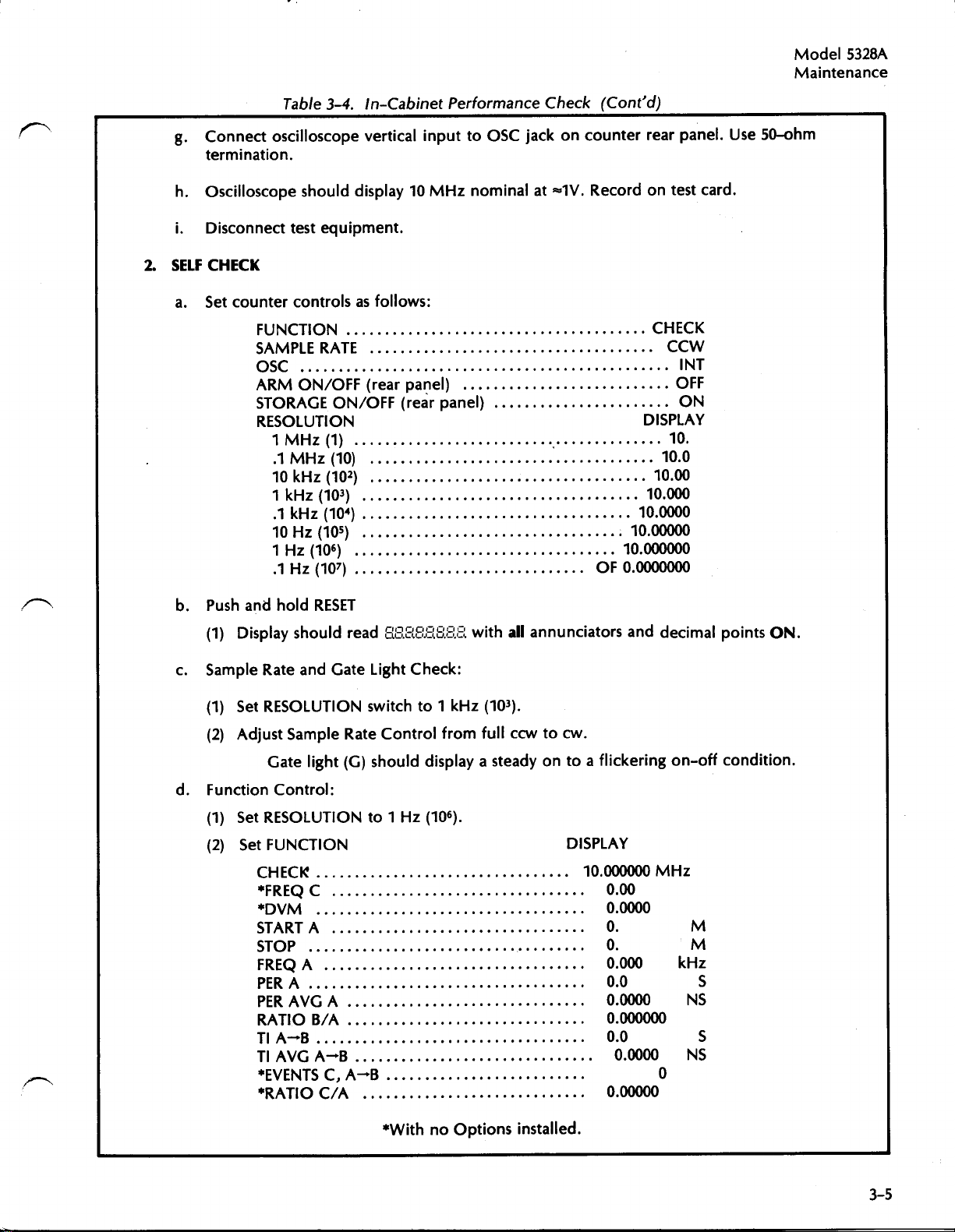
g
.Connect
termination
h
.Oscilloscope
i .Disconnect
2
.SELF
a
.Set
CHECK
oscilloscope
counter
FUNCTION
SAMPLE
OSC
ARM
STORAGE
RESOLUTION
1
.1
10
1
.1
10Hz(105)
1Hz(106)
.1
Table
.
should
test
controlsasfollows
. . . . . .
ON/OFF
MHz
MHz
kHz
kHz
kHz
Hz
.
In-Cabinet
3-4
vertical
display10MHz
equipment
. . . . . . . . . . ... . .
RATE.. . . . . . ... . .
. . . . . . ... . . .
. .
. .
(rear
ON/OFF
(1)..
. . . . . . . . . . . . . ... .
(10)
. .
. . . . . . . . . . . .
. . .
(102)
(103)
(104)
(107) . . . . .
. ... . . . . . . ... . .
. . . .
. ... . . . . . . ... .
. . . .
. .
. . . .
. .
. . . . .
. ... . . . ... ... . . .
. .
Performance
inputtoOSC
nominalatm1V.Record
.
:
. . . . . . . . . . .
. . . . . . . . . . . . . . . . . . .
. ... . . . . . . . . . . . . . . .
panel).. . . . . . . . . . . . . . . . . . . ... .
(rear
panel).. . . . . . . . . . . . . . . ... . .
.
. .
. .
. . . . . . ... . . .
. .
. . . . . . ... . . .
. . .
. . . . . . . . . . .
Check
jack
. . . . . . . .
. . . . . . . . . . . . . . . . . . . . .
. . . . . . . . . . . . . . . . . . . .10.0
. . . . . . . . . . . . . . . . . .
. . . . . . . . . . . . . . . . . .
. .
. .
. . . . .
. . ... . . . . . . . .
. .
. .
. . . . . . . . .
. .
. . .
(Cont'd)
on
counter
. . . . .
. . . ...
. . . . . .10.0000
. . . .
OF0.0000000
. .
.10.00000
10
rear
on
CHECK
CCW
. .
. . .
. . .
. .
DISPLAY
10
.
10
.00
10
.000
.000000
panel.Use
card
test
INT
OFF
ON
.
.
Model
Maintenance
50-ohm
5328A
b
.Push
(1)Display
c
.Sample
(1)
(2)Adjust
d
.Function
(1)
(2)Set
and
Rate
Set
RESOLUTION
Gate
Set
RESOLUTION
FUNCTION
CHECK
*FREQ
*DVM
START
STOP
FREQA
PER
PER
RATIO
TI
TI
*EVENTS
*RATIO
hold
RESET
should
Sample
Control
A.. .
AVG
A-B
AVGA-B
read
LlL4L4LJ`SU~
and
Gate
Light
Check
switchto1
Control
Rate
light
(G)
should
:
to1Hz
. . .
. ... . . . . .
C.. ... . . . . . . . . . . . . . . . ... .
. .....
. . . . . . . . . . . . . . . . . .
A
. . ... . . . . . . . . . . . . . . . .
. . .....
B/A....
. . . . . . . . . . . . . . . . . . . ...
.
. . . . . . . . . . . . . . . . . . . . . .
. . .
.
. ...
. . . . . . . . . . . . . . . . . . . . . .
A..
. . . . . . . . . . . . . . . . . . . . . .
. . . ...
. . . .
. . .
A-B
C,
C/A
. . . . . . . . . . . . . . . . . . . . . . . . . . . . .
displayasteadyontoaflickering
(106)
. . . . . . . . .
. . . . . . . . . . . . . . . . . . . ... . . . .
. . . . . . . . . . . . . . . . . . . . . . . . .
. . . . . . . . . . . . .
. . . . . . . . . . . . . . . . . . . . .
with
all
(103)
ccwtocw
. .
. .
. ...
. . . .
.
. . . .
. . . .
annunciators
. . .
. . .
_
:
kHz
from
full
.
.
. . . . . . . . . . . . . ..0
DISPLAY
. .
.10.000000
. .
. . .0.00
. .
. .
. . .0.0000
. .
. . .0.
. .
. . .
. .
. .
. . .0.000
. .
. .
. . .0.0
. .
. ...
. . . . .
.
.
.
and
0
.
0
.0000
0
.000000
0 .0
.0000
0
.00000
decimal
on-off
MHz
M
M
kHz
NS
NS
0
points
condition
S
S
ON
.
.
*With
no
Options
installed
.
3-5
Page 31

Model
Maintenance
5328A
3.FREQUENCY
Table
3-4.In-Cabinet
RESPONSE
a
.Set
counter
b
.ConnectaBNCTconnector
puttoT
input
Adjust
c
.
amplitude.Counter
card
.
d
.Repeat
maintaining50mV
e
.DisconnectHP608E
andtoChannelBof
f
.
AdjustHP651B
Connect
g
.
controls
connector.Connector
signal
amplitude;usea50-ohm
HP
step3cwithaninput
OUTPUTMARKER
from
651B
rms
and
outputto1000Hzat4volts
AND
SENSITIVITY
as in 1a,
should
oscilloscope
except
toINPUT
10
Hz
to 10
properly
fromHP608E
mV
(141
connectHP651B
Aof5328AtoChannelAof
Performance
RESOLUTION
Ainput
oscilloscope
feedthrough
MHz,
p-p)
.
maintaining25mV
display
all
VHF
.
through
Check
to1Hz
jack.Connect
vertical
frequenciesinthis
Signal
BNCTconnector
peak-to-peak
(Cont'd)
(106)
HP651BTest
inputtoT
at
oscilloscope
Generator
.
oscilloscope
and
AC/DC
connectortomonitor
rms
range.Recordontest
of 10
to
switch to
Oscillator
BNC
.
(70
mV
MHz
to
INPUTAof
.
p-p)
100
AC
out-
input
MHz
5328A
.
h
.Set
LEVELAto
i .Set
j
.Adjust
k
I .
m.Disconnect
4.PERIOD
a
.Set
b
DISPLAY
A
POSITION
should
that
the
.AdjustAPOSITION
Rotate
and
negative
volts
.
Rotate
settabletoat least1.8
Repeat
AND
counter
(103)oras
.Connect
feedthroughatoscilloscope
PRESETand
controlonoscilloscopetoALT
oscilloscope
touch
trigger
LEVELAcontrol
LEVELAcontrol
cable
stepsjthroughIabove
PERIOD
controlsasinstep
needed
HP
for
so
the topofthe
both
the
levelisat0voltsinPRESET
slopeofthe
from
AVERAGE
.
651BtoINPUT
SEP-COM
asymmetrical
positive
so the top
until
waveform
from
volts
below0volts
OUTPUT
BNC
AtoCOM
.
waveform
marker
and
the
fullcwposition to
.
1a,
A,
pulseisat0volts.(The topofthe
the
negative
.)
of
marker
topofthe
MARKER
with
FUNCTION
using
.
.
This
.
BNCT.
pulseisat
indicates
A
A
.
on
ChannelB,centeredat0volts.Adjust
marker
slopeofthe
marker
ccw.Top
and
connect
to
PERAand
Connect
waveform.This
least1.8
pulse
touches
that
the
of
to
oscilloscope
volts
both the
trigger
marker
RESOLUTION
pulse should
OUTPUT
to T,
indicates
above
levelisat
MARKER
using
pulse
0 volts
positive
1
to1kHz
5011
be
B
.
.8
.
3-6
c
.Vary
d
.Set
theHP651B output
RESOLUTION
frequency.Counter
within
accuracy
FUNCTION
from10Hzto10
switch
switchtoPERIOD
as
needed
should
specifiedinTable
properly
MHz,
to
maintain
display
1-3.Recordon
AVGA
and
the
repeat
maintaining25mV
meaningful
periodofthe
test
stepc.
display
frequenciesinthis
card
.
Record
rms
amplitude.Vary
with
change
on
test
card
of
range
.
Page 32

5.TIMEINTERVAL
a
.Set
b
c
.Set
counter
SAMPLE
FUNCTION
RESOLUTION
SLOPE
SLOPE
AC/DC
ATTEN
LEVEL (A
SEP-COM
.Connect
p).Observe
FUNCTION
MHz
(2
one
half
counter should
MHz
Table
3-4.In-Cabinet
AND
TIME
INTERVAL
controls
RATE.... . . . . . . . . . . . .
(A)
(B)
(A
(A
andB). . . . . . . . . . .
HP
651BtoINPUTA.
display
toT.I.AVG
must
the periodofthe
display
±2ns±
follows
as
. . . ... . .
. ... .
. . . . . . . . .
. . . . . . . . . .
and
B)
B)
and
A
. . . . . . . . . . . . . .
for.5us±1count±trigger
NOT
be
500
tr
igger error
Performance
AVERAGE
:
. . ... . . . . .
. . . ... . . . . . . .
. . ... . . . . . . ... . .
. ... . . . . .
. .
. . .
. .
Set
A-B,
input
ns
. . . . . . . . . . .
. .
. . . . . . . . . . .
. ... . . . . . .
. . . . . . . . . . ...
oscillator
RESOLUTION
signal.For
.
±100ns(±1count)
intervals
of
. .
. . . .
exactordisplay
.00
number
Check
. ... . . . . . . . . . . . . .
. . ..... .
. ... . .
. . . . . . . . . . .T.I.A-B
.
... . . . . . . . . . . . . . .1MHz
.
. . . . . . . . . . . . . . . . . .
. . ... . . . . . . . . . . . . .
. . ... . . . . . . . . . . . . .
. . ... . . . . . . . . . . . . . .
. ... . . . . . . . . . .
for 1
MHz
error.Record
to.1kHz
will
be
example,
averaged
(Cont'd)
. . . .
. . . . .
.
outputat150
ambiguous).Counter
with
_
Midrange
COM
(10
4 )
.
a 1
(+)
.
(-)
.
AC
PRESET
mV
on
test
Set
MHz
X1
A
rms
card
signal
should
input
Model
Maintenance
(425mVp-
.
sourceto<2
display
signal
the
5328A
6.TOTALIZE
a
.Connect
Set
counter
b
.Check
Record
c
.Using10:1
panel
rear
d.Check
RESOLUTION
Disconnect
e
.
quency
f
.SetHP651Bto10
HP
651BtoINPUTA.
controlsasfollows
FUNCTION
RESOLUTION
LEVEL
that
on
that
Counter
and
(A
display
test
divider
.
oscilloscope
totalizes,
card
probe,
oscilloscope
switchto.1
input
MHz
. . ... ...
. . . .
. . . ... .
B)
. . .
.
connect
indicates
fromTBOUT
.
at
150
(G)ison
1
Hz
and
jack
(425
for1MHz
. . . . . ... . .
positive
observe 100
and
mV
Set
oscillator
:
. ... . . . . . . . . . .
. . . . . . . . . . . . . . . . . . . .
. . ... . . . . . . . . . . . . . . . . ... . . . . . .
Gate
light
oscilloscope
MHz
(10)
mV
rms
outputat150mVrms
. . . . .
. ..1Hz(10
and
LEVEL
A
vertical
connectTBOUT
p-p)
input
going
kHz
.
START
PRESET
. .
and
B lamps
toTB
pulses
output
(425mVp-p)
A
6 )
flashonand
jackoncounter
OUT
at least3Vp-p.Set
pulses(.1
to
5381A80MHz
ls)
off
.
Fre-
.
.
Page 33

Model
Maintenance
5328A
7
.RATIOB/A
g.Set
Record
a
.Set
Table
RESOLUTION
on
test
card
RESOLUTION
1. .
. . ... . . . . . . ... . .
10. .
. . . . . . . . . . ... . .
102.
. . . ... . . . . .
103... . . . . . . . . . ... . .
104. . . . . . . . . . . .
10
5 . .
. . . . . . . . . .
10
6.
. . . . . . . . . . .
107.
. . . . . . . . ...
counter
controlsasfollows
FUNCTION
RESOLUTION
SLOPE
AC/DC
ATTEN
SEP-COM
LEVELA. . .
LEVEL B
(A
and
(A
and
1-10-100
A..
. . .
3-4.In-Cabinet
as
follows,
.
. .
. . .
. .
. . .
. .
. . .
. .
. .
. .
. . .
. .
. .
. . . . . . . . . . . . . . . . . . . . . ... ...
.
. . . . . . . . . . . . . . . . . . . . . . ... . .
B)
. . . . . . . . . . . . . . . . . . ..... .
B)
. . . . . . . . . . . . . . . . . ..... .
. . . . . . . . . . . . . . ... . .
. . . . . . . . . . . . . . . . . . . . . .
. . . . . . . . . . . . . . . . . . . . . . . . . ... .
. . . . . . . . . . . . . . . . . . . ... . .....
Performance
and
check
. . ... . . . . . . . . . . . . . . . . .
. . .
. .
. . .
. .
. ...
.......
. . ... . . . . . . . . . . . . . . . . . . . .
. . ... . . . . . . . . . . . . . . . ... .
. . . . . . . . . . . . . . . . . . . . .
. . . . . . . . . . . . . . . . . . . .
:
for
proper
. . . . . . . . . . . . . . . . . . .1.0MHz
. . . . . . . ... . . . . . . . . . .
. . ... . . . ... . . .
. . ... . . . . . . . . . . .
. ... . . . . . . . . .
Check
. . . . . .
(Cont'd)
counter
5381A
No
.10kHz
. .1kHz
. .
. .
. .
. . .10Hz
. .
. .
. . . .1Hz
. . . .
RATIO
.1
. . .
. . . . . . . . . .
. . . . . . . . . . .
+
. . . . .
+
display
DISPLAY
Output
100
kHz
100
Hz
B/A
kHz
(104)
. . . .
(+)
. .
AC
. . . .
COM
A
Triggering
Triggering
(approximate)
1
.
b
.SetHP651E
c
.Connect
d
.Display
8.GATE
a
.Connect
b
.Set
c
.Using10:1
d
.Slowly
OUTPUT
counter
a
positive
width
to 10
BNC
cable
should
FUNCTION
RESOLUTION
SEP-COM
SAMPLE
rotate
increases
read1.0000,
AND
SAMPLE
equipment
controlsasfollows
RATE
divider
pulse
>_2
SAMPLE
.
MHz
at1Vrms
from
OSC
RATE
as in
step7cabove
. . . . . . . . . . . .
. . . . . ... . . .
A
. . . . ..... .
. . . .
probe,
.4V
connect
withapulse
RATE
.
BNC
on
depending
:
. . ... . . . . . . . . . . . .
. .
. .
. . . . . . ... . . . ... .
. . . . . . . . . . . . ... . .
. .
. .
. . . ... . ... . . ... . .
oscilloscope
widthof<_10ms.
clockwise
and
rear
paneltoINPUT
on
accuracyoftest oscillator
vertical
observe
disconnect
. ... . . . . .
. . ... . . . . . . . . .
. . .
. .
inputtoGATE
Record
that
the
except
HP
.1
MAX
. .
negative
Aon
FREQ
kHz
on
front
setting
.
6518
A
(104)
SEP
CCW
OUT
test
card
portionofthe
panel
.
and
.
.
observe
pulse
3-8
Page 34

HEWLETT-PACKARD
UNIVERSAL
COUNTER
SerialNo.
1 .
TIMEBASE
Aging
Rate:<3
Output:10
2.DISPLAY,
As
per
self-check
3.FREQUENCY
FrequencyARange:0to40
STABILITY
MHz,
DECIMAL
RESPONSE
PERFORMANCE
MODEL
5328A
DESCRIPTION
AND
OUTPUT
partsin107per
(square
-1V
POINTS,
procedures,
AND
MHz
40
(141
(RefertoTable
month
wave)
AND
DIVIDERS
Table 3-4
SENSITIVITY
MHz
at25mV
to
100
MHz
mV
p-p)
CHECK
Test
at50mV
TEST
Performed
3-4)
(70
mV
p-p)
CARD
by
Date
CHECK
Model
5328A
Maintenance
ChannelAPreset:OV
ChannelALevel:+1.8to -1
ChannelBPreset
ChannelBLevel:+1.8to -1
4.PERIOD
5.TIME
TOTALIZE
6
.
AND
Frequency
INTERVAL
Time
Interval:0
Interval
Time
PERIOD
Range:0to10
AND
Average:1
Range:0to10
Output
Factor:1
7
.RATIOB/A
Per
Rear
:
to 107in
Table3-.4,
:
OV
AVERAGE
TIME
Asat150
.5
/
MHz
panelTBOUT
decade
Step
7
.8V
.8V
MHz
at25mV
INTERVAL
AVERAGE
mV
2
periodofinput
BNC
(for
steps
(70
N>1)
mV
signal
p-p)
GATE
Per
OUTPUT
Table
8
.
3-4,
AND
Step
SAMPLE
8
RATE
:
3-8a
Page 35

3-22.ADJUSTMENTS
3-23
the
Adjustment
.
standard
a
.A
b
.The
time
trouble
instrument
(In-Cabinet
3-24
Oscillator
.
When
C18
adjust
3-25
.Periodically,
required,
oscillator
the
use
the
until
procedures
interval
has
unit
been
does
Performance
Adjustment
adjusting
(see
Figure
FREQ
the
oscillator
oscilloscope
the
movement
are
provided
(sensitivity).The
repaired
not
meet
Check)
which
specifications
all
or
(StandardorOption
NOTE
standard
the
ADJ
method
6-6)
on
When
.
the
should
of
adjusting
10544A
bechecked
shown
patternisstopped
the
for
the
adjustments
would
during
5328A
crystal
below
standard
should
affect
these
whileperforming
periodic
010)
oscillator,
the
Option
oscillator
toahouse
.
Using
the
or
and
Option
notbedone
values
calibration
adjust
capacitor
oscillator,
010
unit
.
standard.When
appropriate
nearly
010
.
the
.
sweep
stopped
oscillator
unless
and
:
checkinTable
adjustment
speed,
.
Model
Maintenance
for
3-4
is
adjust
5328A
3-26
3-27
Sensitivity
.
.
Adjust
Remove
a
.
Attenuator
b
.
Set
MOVEMENT
1
CM/SEC
1CM/IOSEC
1
CM/100
SEC
Adjustments
sensitivityasfollows
the
top
coverof5328A
Assembly
counter
front
FUNCTION
RESOLUTION
SLOPE
AC/DC
ATTEN
LEVEL
SEP-COM
SAMPLE
CALIBRATION
SWEEPSPEED
IgSEC/CM
1
X
1
X10
1X10⁻⁸
10-6
0
.1pSEC/CM
1
X
1X10
1X10
10-7
8
-9
0
.01g
1X10
1X10
1X10
SEC/CM
-8
-10
TIME
SCOPE
9
TRACEMOVEMENT
WITH
SECOND
WATCHORCLOCK
OF
:
locator)
. .
. . . ...
. . . . ...
. . .
. . . . . .
resistorsR3andR18
. .
to gain access to
(see
Figure
controlsasfollows
panel
. . . . . . . . . . . . .
. . . . . . . . . . .
(A)
. . . . . . . . . . . . . . . ... . . ... . . .
(A)
. . . . . . . . ... . . . ... . . ... . . . . ... ...
(A)
. . . . . . . . . . . . . . . . . . . ... . .
6-12
component
:
. .
. . . .
. .
. . .
variable
. .
. . .
A.. . . . . . . . . . . . . . . . . . . . . ... . . . . ... . .
A
. . . ... . . . . . . . . . . . . . ... . . . ... . .
RATE.. . . . . . . . . . . . . . . ... . . . . .
.
NOTES
HAND
.
FREQ
106
1
. ...
. .
. .
. . . . . .
PRESET
COM
Midrange
DC
Hz
on
the
A19
A
+
1
A
3-9
Page 36

Model
5328A
Maintenance
c
.Set
counter
rear
panel
STORAGE
OSC
. . . . . . . . . . . . . . ... . . . . . . . . .
d
.
Connect
MHz
e
.Decrease
counter
f
.
To
check
ARM
HP
at50mV
signal
display
ChannelBchange
608
Signal
rms
generator
for stable
...
.
FUNCTION
RESOLUTION
SEP-COM
With
signal
9
.
generator
generatortoINPUTBsetto40
h
.Repeat
R18
.
stepeand
observe
controls
as
follows
. . . . . . . . . . . . . . . . . . . . .
. . . . ... . . . ... . .
Generator
output
correct
settings
... . .
. . .
.
. . . . . . . . . . . . . . . . . . . . . . . .1kHz103
A
. . . .
. . . . . . . . . . . . ... . . . ... . . . ... .
connected
MHz
display
. . .
(or
equivalent) to
level
slowly
indication.If
of
front
. . .
. . .
. . .
to
INPUTAsetto10
at50mV
for
correct
:
. . . . . . . . . . .
. .
. .
. . . .
to
panel
. . ... . . .
rms
ratio
. . .
. . .
. . .
. .
.
. . .
. .
. . . ... . . .
INPUTA.
25
mV
rms
necessary,
adjust
controls
RATIO
MHz,
.
indication.If
ON
INT
OFF
Set
signal
(70
mV
resistorR3.
as
follows
B/A
.
SEP
connect
necessary,
generatorto40
p-p)
and
observe
:
a
second
adjust
resistor
signal
3-28
.
INSTRUMENT
3-29
.Trouble
controls,
conducting
connectors,
the
TROUBLESHOOTING
isolation
and
in-Cabinet
trouble.Troubleshooting
3-30
.
TROUBLESHOOTING
3-31
.
Troubleshooting
section.The
following
table
for
3-32
.
3-33
.This
021.It
signals
a
.Extender
b
.Extender
use
of
paragraphs.This
IC
troubleshooting
DVM
Extender
kit
consistsofthree
allows
with
circuit
the
appropriate
board
assembly
for
board
Option
extended
021.(Assembly
duetospace requirements
extender
assembliestobe
Option
can
best
be
indicatorsonthe
Performance
aids
are
AIDS
flowcharts
boards
section
.
Board
Kit
(05328-82020)
extender
test
equipment.The
(05328-62020)
020 or
(05328-62021)
A5
accomplishedbyobtaining
5328A.This
Check
(Table
describedinthe
for
each
assembly
and
test
cards,
also
containsatable
boards
that
extended
with
one
15-pin
021
.
with
one
15-pin
must be
placed
information
3-4)toaidindetermining
following
of
the
availableasservice
for
are
used
from
their
kit
includes
and
connector.Extends
on
its
.)
all
possible
paragraphs
5328A
are
analysis
for
servicing
plug-in
the following
one
18-pin
extender
information
should
then
be
symptoms
.
provided
at
the
kits,isdescribed
of functional
DVM
Options
connectors
for
:
connector.Extends
A6orA7
board
before
from
analyzed
of
backofthis
in
signals
and
020
monitoring
assembly
A6
can
the
by
the
the
a
and
AS
for
be
c
.Extender
boardofOption
together
board
.
(05328-62022)
021
.
Has
cable
for
frontofassemblies
attachedtoconnect
A5
front
andA6.
Simulates
connectorsofA5
front
panel
and
A6
Page 37

3-34
.Extender
3-35
extender boards
Frequency
the
3-36
3-37
the
troubleshooting
3-38
nectorsoneach
inserted
test
and4.
tests5,6,7,and8on
Part
This
.
standard
.Function
.This
ROM
.The
into
connections
The
numbers
a.Test
Test
b
.
c.Test
d.Test
Board
typeofextender
are
Assembly.One
C
5328Aorthe
Selector
kitisusedtoreplace
the
on
flowchart
four
test
card.The
Motherboard
A1
showninthe block
four-edge
of
the
Card
Card2,05328-22004
Card3,05328-23004
Card4,05328-24004
(05328-62016)
boardisavailable
required
motherboard
cardsinthe
connectorsoneach
Card2,tests
cards
1,
05328-21004
extend
to
of
these
A10orA14
and
ROM
theA4Function
withaROM
forA1motherboard
kit
tests
are
connector
are
as
separately
theA4Function
extender
assembly
Kit
provideatotalof16
describedinparagraphs
diagram
9,10,11,
follows
boardsisrequired
for
Option
(05328-82004)
Selector
simulator
andisdescribedinthe
XA4toreplace
for
each
card
are
numbered
and12on
:
Card3and
(not part ofaservice
Selector
Assembly
card.Useofthis
tests,
the
test.The
040
one
3-45
Function
A4
with
Assembly
to
extend
.
withatest
for
eachofthe
through
test
cards
tests1,2,3,and4on
tests
13,14,15,
kit).Two
the
or
theA10assembly
card
kitisrequiredinthe
following
four-edge con-
3-115.The
Selector
are
numbered
and16on
of
Option
or to
replace
paragraphs
cards
assembly
1, 2,
Card
Card
030
Model
Maintenance
these
with
A8
for
are
3,
1,
4
5328A
.
.
3-39.The
8120-2176.The
three
from
Useofthe
3-40.USINGTHE
3-41
.The
the
5328Aasdescribed
.Eachofthe
3-42
edge,
3-43
.
tested
3-44
.To
display
ROM
card
IC's,
andaconnector
oneofthe
ROM
test
cards
respectively.The
A
descriptionofthe
and
procedurestoperform
perform
.
Simulator
and
connectorstothe
card
Simulator
TEST
describedinparagraphs
following
TURN
INSERTING
any
To
diagrams,
6-17,A1Motherboard
card
cable
are
supplied
for
eachIC.
cardisdescribedinA1
CARDS
the
following
in
listed test
cards
are
keyed
purposeofthe
OFF
CARDS
the
check
following
the
refertoconnector
of
(05328-65005)isused
with
this
Service
The
card
replaces
are
POWER
test
card
provided
connector
paragraphs
prevent
to
test,
CAUTION
.
tests,
connections
for
Motherboard
3-34
and
.
and
test
numbers
incorrect
a
block
for
each
BEFORE
insert
the
NOTE
XA4(A
Interconnection
in
conjunction
kit.The
ROM
A1U37
A1U37
ROM
3-35
are
used
are
insertion
diagramoftest
test
.
REMOVING
appropriate
in
and
Diagram
the
B) in
shown
with
Cable
ROM
simulator
connecting
by
(after
removing
Troubleshooting
to test
various
labeledonthe
into
test
connector
connections
OR
test
card
and
block
Figure
.
Assembly
contains
card
the
the
ROM)
Flowchart
functions
card
and
of
circuits
observe the
cable
of
card
XA4
.
.
.
Test
3-45
.
3-46
.Description.I
checked
wishes-to strobe
Card1,Test1,Low
This
lineisusedinmost
.
n
this test
different
data
Disable
the
abilityofthe
test
into
the
Decade
card
displayorblank the
tests
Counting
LDDCA
and
during
Assembly
linetodisable
normal
operation
display
.
(LDDCA)
the outputofthe
when
any
DCA
module
is
3-11
Page 38

Model
5328A
Maintenance
3-47
3-48
3-49
.Block
diagramoftest
.Procedure
.Display
:
Set
results
FUNCTION
:
connections
switch
NLI/
:
to
XA4
CHECK
.
3-50
.Test
3-51
.Description
Function
Selector
3-52
3-53
3-54
MHz
MSD
Selector
.
.Block
FS
OSC
.Procedure:Set
.Display
whenN=10
triggers
Card1,Test
.
With
being
diagramoftest
_
A14
XA4
FUNCTION
results:the
.
AsNis
OVFL
indicator
2,
DCA
and
this
test,
used,
enabling
connections
814
MSD
on
increased,
after
Time
Base
both
the
DCA
problem
:
TBI
TIME
BASE
switchtoCHECK
the
the
the
display
first
should
displayed
cycle
and
Time
Base can
be
checked
isolationtoA1 Motherboard
814
XA4
A16
XA4
A15
TBO
.
totalizeata
digits
will
rateof10
decreaseindecade
.
_
MHz
without
orA4Function
FDD
when
steps
DCA
N=1
of 10.The
the
and
A4
1
3-55
.Test
3-56
.Description:If
MHz
at
the
first
cycle
.
Card1,Test3,Decade
the
DCA
correct
rate.The
MSD
Counting
is
suspectedtobe
should
totalize
Assembly
faulty
and
(DCA)
this
test
trigger
will
the
determine
OVERFLOW
if it
will
count
indicator
after
10
its
Page 39

.
3-57
3-58
.
3-59,
3-60
.
3-61
.
correct
3-62
.
Block
diagramoftest
FS
OSC
A14
Procedure:Set
Display
Test
results:Display
Card1,Test4,Time
Description.This
.
Block
diagramoftest
connections
X
A4
~~
FUNCTION
test
will
connections
A15
FDD
switchtoCHECK
should
Base
show
Code
totalizeat10
whether
Model
5328A
Maintenance
:
FDC
.
MHz
.
the
Time
Base
code
goingtothe
Time
Base
is
:
3-63
.
Procedure:Set
RESOLUTION
1
10
102
103
10
10
10
10
TO
DISPLAY
below
FUNCTION
switchtoCHECK
Table
for
Test
4
5
7
and
Card1,Test
DISPLAY
1 1 I 1 1 I I I
1 I 1 1 I 1 1.1
-I-1-1-
I
-1'_I
1 1 I
I~_I
I
1
_
1_
-I-
1
I 1
I
.-II_ I_ I_
=' _'
I
I
I_1 I_I
-I
I II,I I I I
I I
I III 1 I
1 1 1 I 1 I I 1
I I I I
I
.
RESOLUTION
4
-
1
_I
I_
.I_
1 I
I
IJ
1 I'-1
I
I
as
shownintable
NOTE
If
Option
the
040isinstalled
displayed
willbei-''s.
digits
:
Page 40

Model
5328A
Maintenance
3-64
3-65
a faultless
3-66
.Test
Card2,Test5,Function
.Description:This
display
.Block
.
diagramoftest
Code
test
canbeusedtoverify
connections
:
and
Display
the
Function
Codeoras
the
rapid
waytoverify
FUNCTION
SWITCH
DCA
3-67
.Procedure:Set
RESOULTION
positionaslistedintable
FUNCTION
Check
Freq
C
below
FA
FB
FC
FD
switch
.
Table of
DISPLAY
1111
I_I 1I-111
I 1I1,
'
'-'-'-I-,-1-'-
1_ 1_ 1_ 1_
I_,1_I-1_
B11
B10 818
B13
B12
Test
1 I 1 I
XA4
kHz
to
.1
Card2,Test
-1
'-
~_
Ninth
B17
B15
816
(10
and
4
)
5
digitifOption
set
DATA
BUS
FUNCTION
NOTE
switch
to
030isinstalled
each
.
DVM
START
STOP
*START
*DVM/A
*DVM,
FREQ
PER
PER
RATIO
TIA-B
TI
AVGA-B
EVENTS
RATIO,
A
CLOCK
A-"B
A
A
A
VG
A
B/A
I
I I III,1I
=~
=1 _~ _~ _~ =1
-'-'
'"'''=
1-
~=
~-1=~_
_
I1_III-I11_
I
=I
-'
-' -' -1 -'-'-' -'I I I 1 1
Cl
_"'
I I II,I II1
11-11=11=11=11=11=1
1II
I I-f
1- I- 1=1-1=
C
li
11
.11
.1-I-1=
I 1-I
11_1,=1
.11
L-1
I
1= 1=
1,1_1
"_'
-1
The "phantom"
I
-
='
'
positions
switch
located
tions
-1
1
respectively
of
that
1, 2,
clockwise
.
(unmarked)
the
FUNCTION
follow
(*)
and3switch
from
are
posi-
STOP,
C,A-B
Ninth
C-A
digitifOption
030isinstalled
.
Page 41

.Test
3-68
3-69
.
on which
Card2,Test6,Strobe
Description
each
suspectedtobe
3-70
.
Block
diagram
I
This
:
test
Code
displays
the
Display
display
digitisstrobed.Thisisuseful
faulty
.
of test
DIGIT
STROBE
BUS
DCA
connections
DSA
DSB
DSC
DSD
LDDCA
:
816
B18
V
B15
B17
A16
strobe
in
checking the
XA4
code(Dbit
display
B17
B18
815
816
A14
DA
DB
DC
DD
grounded) showing
DATA
BUS
Function
the
when
Model
Maintenance
the
code
code
is
5328A
3-71
.
Procedure:Set
.
3-72
3-73
3-74
Display
.Test
.
Description.This
the higher
3-75
.
Block
FUNCTION
results:Display
should
Card2,Test7,Strobe
test
displays
order
codestobe
diagramoftest
DISPLAY
STROBE
COUNTER
DCA
displayed
connections
switchtoCHECK
read
Code
II
the
strobe
.
:
DSA
DSB
DSC
816
B18
815 B15
/~.c
Display
code
XA4
(OPEN)
and
except
B17
B18
816
Q
RESOLUTION
that
the
DA
D8
DC
DO
switchto1Hz(106)
bitismade
D
DATA
BUS
high,
.
allowing
3-76
3-77
.
Procedure:Set
.
Display
results
:
FUNCTION
.
C1n
~_
--`~'-~
Ninth
switchtoCHECK
J
NOTE
digitifOption
and
030
installed
RESOLUTION
.
switch
1Hz(10
to
6 )
.
Page 42

Model
5328A
Maintenance
3-78
3-79
Selectorinthe
A4
3-80
Test
.
.
Function
.
Card2,Test8,AutoSample
Description.This
Selector
Block
diagram
FS
OSC
test
instrument,
.
The
of
XA4
A74
allows
thus allowing
Time
Base output
test
connections
B14
TBI
the
SAMPLE
Sample
TIME
BASE
RATE
Rate
Rate
for fault
simulates
:
circuitry
isolation
LMG
LINH
HRD
LTR A12/--~
between
the
opening
A17
A12 816
A13
tobetested
theA1Motherboard
and
closingofthe
B14
XA4
TBO
B17
B16
B16
withoutanA4Function
and the
main
gate
DA
DB
DATA
DC
DD
BUS
.
3-81
.
SAMPLE
3-82
.
sequence
Procedure:Set
RATE
control
Display
of
-~
L
.MGF
LINH
results:All
HRD
LTR
FUNCTION
approximately
digits will
_
DCA
switch to
read
I-
I
I
I
CHECK
and
RESOLUTION
midpoint(1O'Clock)
the
same
.
They
_
I I
I
I
I
I
I
I
I
.
will
continuously
I
I
-
I
I
I
I
I
I
I
~
I I I
I
I
I
I
I
I
I
I
I
I
I
I
I
n
I
I
I
switchto1Hz(106).Set
cycle
through
I
I
I
I
I
I
I
I
I
I
I
I
the
Page 43

3-83
.Test
3-84
.
Selectorisusedtoestablish
tion
3-85
.Block
Card3,Test9,Function
Description.This
Diagram
A1
MOTHERBOARD
ROM
BITS
test
of test
DCA
Selector
tests
the
ROM
the
main
connections
LMGF
LTIF
HOPN
LDDCA
~J
A14
bits
gate
:
87
B3
B5
A4
Main
that
signal
~L
Gate
help
XA4
ROM
determine
.
817
CT
B18
B15
B16
A16
Bits
DA
DB
DC
DD
(LMGF,
which
LTIF,
signal
DATA
BUS
HOPN)
on
theA4Func-
Model
5328A
Maintenance
3-86
table
Procedure:Set
.
that
follows
FUNCTION
CHECK
FREQ
DVM
START
STOP
*START
*DVM/A
FREQ
*DVMA-B
PER
PER
RATIO
TI
A-B
TI
AVG
EVENTS
RATIO
.
C
A
CLOCK
A
A
AVGA
B/A
A-B
C,
C/A
the
A-B
FUNCTION
Table
and
RESOLUTION
for
Test
switchestothe
Card3,Test
10
0
I
'
'-,
9
RESOLUTION
positions
10'
showninthe
-10
7
1
__
*Phantom
Functions
.
Page 44

Model
5328A
Maintenance
3-87
3-88
and
3-89
3-90
table that
.
Test
Card3,Test 10,A4Function
.
Description.These
Clock
inputofthe
.
Block
Diagramoftest
MOTHERBOARD
ROM
.
Procedure:Set
follows
.
A1
BITS
FDCA
Main
the
ROM
bits
GateFF.
connections
LDDCA
FUNCTION
Selector
determine
:
HTBA
HTBB
HTBO
A14
and
Time
which
XA4
B9
B6
B4
A4-~
RESOLUTION
Base
Input
signal
goestothe
B17
818
815
B16DO
A16
switchestothe
ROM
DA
DB
DC
Bits
(HTBA,
inputofthe
DATA
BUS
positions
HTBB,
HTBO)
Time
Base
showninthe
FUNCTION
CHECK
FREQ
DVM
START
STOP
*START
*DVM/A
*DVM
FREQ
PER
A
PER
AVG
RATIO
TIA-B
TI
AVGA-B
EVENTS
RATIO
C
A
A-B
A
B/A
C
C/A
CLOCK
A
A-B
10
I~
L1
L
I
I
ID
(
_I
'
II
I
LI
L
1
L
Ll
1-1
L
1_I
1-0
for
Table
Test
Card3,Test 10
RESOLUTION
0
10
1
L1
I
I
1
1
I
I
1
1
I
1
;
1
I
I
'-'
1
L
I
1
I
I
.I
II
I;111
1-
;
I, 1I
I
'
LI
L
I
L
I
1
It
/
I
L
102-10
I
I
L1
LI
I_1
II-I,1
Ll
I
'
LI
LI
L
7
(103)
1
I
I
I
I
tt
11
1
I
I
I
I
(104)
I
~~
1
1
I,III
I,
I.1
(105)
rll
1
I
I,I
(106)
I
I
(107)
.
I
~~
L1
.111
I
I
1
1
1,
f
'-1
u
I
1_
L
I
1
=1
I_
I
~
*Phantom
t
Lower
tt
102
only
Functions
number
for
Option
040
.
Page 45

3-91
.Test
RQLTOT),
3-92
.Description.The
for
the
and
also
3-93
.Block
Card3,Test
R(LST),
totalize
blank
11,A4Function
RL4(HDVM)
ROM
mode
functions.HDVM
portionsofthe
diagramoftest
A1
MOTHERBOARD
ROM
BITS
line
LTOT
display
.
connections
RL(LTOT)
R(LST)
RL3(HDVM)
LDDCA
Selector
turns
enables
:
B13
B3
B4
A4
-
A14
Totalize
storage
the
XA4
~-
DVM
ROM
off
to
B17
B18
B15
816
A16
Bits
and
disables
strobeina
Model
5328A
Maintenance
and
DVM
Enable
the
sample
minus
DA
DB
DATA
DC
DD
BUS
sign to
rate
the
Bit
ROM
circuitry
display
3-94
.Procedure:Set
table
that
follows
.
FUNCTION
CHECK
FREQ
DVM
START
STOP
*START
*DVM/
*DVM
FREQA
PER
A
PER
AVG
RATIO
TI
A-B
TI
AVG
EVENTS
RATIO
the
C
A
CLOCK
A-B
A
B/A
A-B
C,TIA-B
C/A
FUNCTION
Table
and
RESOLUTION
for
Test
switches
Card3,Test
1
0
1 1
1
1
-1
to
11
R
ESOLUTION
the
position
10'
showninthe
107
-
1
I
1
1
*"Phantom"
Functions
Page 46

Model
5328A
Maintenance
3-95
3-96
Function
3-97
3-98
table
.Test
Card3,Test
.Description.These
Selector
.Block
.Procedure
that
follows
.
diagramoftest
A1
MOTHERBOARD
ROM
BITS
:
Set the
.
12,A4Function
ROM
lines
determine
connections
RLIIA)
RLIIB)
RLIIC)
LDDCA
FUNCTION
Selector
:
B9
B12
B6
A4
"
A14
and
RESOLUTION
rte_
High
which
XA4
Speed
v
ROM
input
lineisselected
B17
B18
816
816
A16
DA
switchestothe
Bits
(IA, IB,
DB
DATA
DC
DO
position
BUS
IC)
by
on
U6
showninthe
the
A4
*"Phantom"
t
Second
CHECK
FREQC
DVM
STARTA
STOP
*START
*DVM/A
*DVMA-B
FREQA
PER
RATIO
TIA-B
TI
EVENTS
RATIO
Functions
number
FUNCTION
AVG
B/A
AVGA-B
C/A
for
CLOCK
A
C,
A-B
Option
040
Table
.
for
Test
Card3,Test
10
'-
I~
LI
-1
1-
I
'-
1II
'
=1
'
I I
12
RESOLUTION
0
I
I
10
I_I
1
I-
I
~
I
'
=1
I
102-
107
~
I
I
I
-
I
U
I
f
-
-!
I
t
'
'
f
I
I
'-
_
t
I
I
y
I
'
1
I
L
I I
I_
I
'-
'
-
-
I
I
I
In
RATIO
only,
position 101will
side,
position 102-107
for
left
each
C/A,
position
NOTE
position100
add
a decimaltothe
will
adda,0
until at107
will
display_;as
and
display
MSD
right
hand
decimaltothe
will
be
Page 47

3-99
3-100
Test
.
.Description
defined
Card4,Test
by the
following
.
These
13,
Arming
three
table
ARMING
ARMING
:
ROM
bits
Table
(Rear
N
FF
Bits
(A0,
determine
for
which
Arming
ARM
SWITCH
Panel)
0 0 0
0
0
0
1
1 0
1
1
A1)
ROM
A1
0
1
1 1
0 0
1
1 1
and
ARM
signal
Bits
AO
1
0
1
0
the
CH
CH
CH
CH
FREE
FREE
C
CHA
Switch
counter
C
B
B
B
RUN
RUN
ARM
should
Model
Maintenance
triggeronas
5328A
3-101
.Block
diagramoftest
connections
ARM
SWITCH
S3
LDDCA
-
:
A4
A14
XA4
b61!
B16
A16
DB
DATA
BUS
DD
Page 48

Model
5328A
Maintenance
3-102
that
"
.Procedure:Adjust
follows
.
FUNCTION
CHECK
FREQ
C
DVM
START
A
STOP
*START
CLOCK
*DVM/A
*DVM
FREQ
PER
PER
RATIO
TI
TI
EVENTS
RATIO
A
AVGA
A-B
AVG
A-"B
A
B/A
A-
"
C,TIA-B
C/A
B
the
FUNCTION
Table
-
for
and
ARM
ARM
switchestothe
Switch
Test
ARM
position
SWITCH
OFF
'_,
"D
'_
Y
'-
I I .
'=
I~
I
(-
in
~~
shown
ON
I='
1
L
Ll
L
in
the
table
f
'
I
I
'
*"Phantom"
3-103
.Test
3-104
.
the syncronizers
compensation
positions
Card4,Test
Description.The
make
and
synchronizertosend
ROM
line
RL2(BIL)
TI
AVG
3-105
A-"B only
.Block
.
diagramoftest
MOTHERBOARD
ROM
.
When0'sare
decimal,
a period
100
programs
14,
ROM
a TI
measurement
MHz
the
except
Auxiliary
bit
measurement
on
connections
A1
BITS
NOTE
displayed,
the
first,
ROM
all
are
Bits
thosetothe
blanked
RL6(HC),
RL6(HC)isusedtoprogram
when
true.When
will
be
made.The
the
A14
Multiplier
lines in
the
PER
Assembly
:
XA4
RL6(HC)
RL5(TIO)
RL2(BIL)
B1
B2
-d---b4
B5
Jill
A4
f
-
.
AVG
(Option
B17
B15
816
leftofthe
RLS(TIO),
hysteresis
false,
ROM
A
function
040
DA
18
DB
DC
DO
RL2(BIL)
compensation
there
will
be no
line
RLS(TIO)
(Option 040
only)tojitter
DATA
BUS
and
hysteresis
tells
only).The
its
output
have
the
in
DCA
Page 49

3-106
.Procedure:Set
FUNCTION
CHECK
FREQ
C
DVM
START
A
STOP
*START
*DVM/A
*DVM
FREQ
PER
PER
RATIO
TI
TI
A-B
A
A
AVG
B/A
A-B
AVGA-B
EVENTS
RATIOC/A
FUNCTION
CLOCK
A
C,
A--B
and
Table
RESOLUTION
for
Test
switchesasshown
Card4,Test 14
RESOLUTION
10
0
f I
'
'
Ll
-'t
'
'
in
table
101-10
that
'
'
Model
Maintenance
follows
7
5328A
:
*"Phantom"
tLower
3-107
3-108
number
.Test
.Description.ROM
play.CARM
3-109
.Block
for
.
Option
positions
Card4,Test
tells
theA4Function
diagram
MOTHERBOARD
A1
ROM
MODULE
C
F
15,
bit
of test
BITS
DCA
040
.
Module
C
HEC
enablesthe
Selector
connections
RLI(HEC)
M
C
RA
LDDCA
(ROM
Bit
HEC
ChannelCmodule
that
the
C Module
:
XA4
B7
A6
4
-
i--~_
A14
and
CARM)
B17
818
815
A16
to
strobe
triggering
is
DA
DB
DC
DD
its
digit
(CARM
DATA
BUS
into
high)
the
dis-
.
Page 50

Model
5328A
Maintenance
3-110
follows
.Procedure:Set
.
the
FUNCTION
Table
switch
for
Test
trigger
and
Card4,Test
ChannelCas
15
DISPLAY
showninthe
table
that
*"Phantom"
FUNCTION
CHECK
FREQ
DVM
START
STOP
*START
*DVM/A
*DVM
FREQ
PER
A
PER
AVG
RATIO
TI
A-B
TI
AVGA-B
EVENTS
RATIO
Positions
C
A
A-"B
A
C/A
CLOCK
A
B/A
C,
A-B
C
NOT
NOTE
MODULE
TRIGGERING
I_I
'
I
I
I
;-
;
I
I
I_
I
I I I
I
I
C
MODULE
TRIGGERING
I-
_
=
1
I
_
I=1
-
I
I
='
I='
I
-
I-
3-111
.Test
3-112
.Description.These
Data Bus
3-113
.Block
Card4,Test
.
F
CODE
TheCmodule
same
effect
the
bus
.
16,
Function
lines
diagram
of test
FA
FB
FC
FD 812 B16
connections
A17
810
813 B15
triggersifinstalled.If
is
obtainedbygrounding
are
Selector
sent to
the
Digit
DCA
:
XA4
817
B18
FDA
FDB
FDC
FDD
(FDA,
where
not
installed,
the
CARM
FDB,
they
DCA
line
FDC,FDD)
are
latched
the
of
and
strobed
XA4
onto
the
Page 51

.Procedure:Set
3-114
3-115
.Display
shown
below
Results
.
CHECK
FREQC
DVM
START
STOP
*START
*DVM/A
*DVM
FREQ
PER
PER
RATIO
TI
TI
EVENTS
RATIO
FUNCTION
Observe
:
FUNCTION
A
CLOCK
A-B
A
A
AVGA
B/A
A-B
AVGA-B
C,TIA-B
C/A
switchtoeach
only
the
for
Table
Function
Test
Card4,Test 16
position
Selector
listedinthe
digit
(2nd
DISPLAY
from
=
'-(
=
'_
table
right).It
that
follows
shouldbeas
Model
Maintenance
5328A
.
*"Phantom"
3-116
3-117
IC
.
.To
Set the
a
.
b
.Set
c
.Remove
d
.Apply
positions
Troubleshooting
troubleshoot
FUNCTION
the
FREQ
top
power
10528A
Logic
the
IC'sonthe
switch
RESOLUTION,
cover
and
remove
and
check
Clip oraModel
for
to
the
CHECK
N
10525T
Motherboard,
A1
.
switchto1
A4
Function
logic
states as
Logic
proceedasfollows
MHz1.
Selector
showninTable
Probe.A
Assembly
dark
pattern
.
3-5,
usinganHP
indicates
:
Model
logic
high
a
.
Page 52

Model
5328A
Maintenance
5328A
(See
U22
U23
U24
U25
Display
preceding
1
ISIONNEON
""""""""
101 16
1
"1[3
101w*
11
miommoomD
""""""
10
1
Lo"
10 16
:
initial
When
patterns
lineonthe
1
I
I
* * 8
""""
1
130000
o00[3
Table
3-5.IC
Troubleshooting,
~',~ ~~-f
conditions)
NOTE
checkinga14-pinICwith
for
pins
8
and9of
pattern
.
"
*
""
mom
16
8
O
"
16 10
8
"D
14
14
16
14
PIN
PIN
PIN
PIN
the
the 16-pin
Logic
Clip as
Al
Motherboard
logic
shown
U32
U33
U34
9th
digitisfor
clip,
ignore the
by
the dotted
1
*
""0""e""
10
*
11
":0
"
1
0
1
I
1~
10:
0050000
":0""
101
Option
1F
* 8
""
0"13"
""
00
""
00
""
030
8
16
16
1
18
Installed
16
PIN
14
PIN
14
PIN
U26
U27
U28
U29
U30
U31
1
"0""
0"13"
O"000000
10
1
""0"
10
10
1
D
0000
"
"
0" "
130
* * 8
""""""
16
""""""""
10
* *
*
11
INION00001111111
Mismosommi
10
:
1
0:0"""""
"""""
10
1
**
1
O[3
"
00
10 18
**8
D
""
+1r
"0
16
0
16
"
8
16
PIN
16 10 16
8
16
PIN
D
16
8
8
14
14
16
16
PIN
PIN
PIN
PIN
U35
U36
U38
U39
U40
U41
11
":0"
00
""
I
11
*
";0""
101
11
i
"1"""
10
1
O
10 18
1
"
1
i
o
10
1
1
O
10 16
:13
"0""
I
1
0
""D""
;
"""
13
"""
l]
0"
**
0[311
0
13D
""
0"
0
8
0
8
16
0
"
18
8
8
14
14
14
16
14
PIN
PIN
PIN
PIN
PIN
"
16
16
PIN
*Indicates
3-26
dimly
lit
Page 53

PINS
U25
Table
Y
W
=
U
3-5.IC
U
,
O
LLJ
u
.
Troubleshooting,A1Motherboard
FUNCTION
Y
U
O
m
U
¢
w
a
>
0
cn~%*
cn
¢i< U
¢ 2 2
*
Model
5328A
Maintenance
(Continued)
m
Q
m
v
.
Q>Q
O
WdW
o
u
.
a
m
w
Q
¢
N
U
Q
u
Q
U
O
>
w
INPUTS
OUTPUTS
INPUTS
OUTPUTS
INPUTS
U26
U27
6
9
10
15
16
2
3
6
7
9
10
15
16
3
6
7
L
L
2
3
7
2
H H
H
H
H
H
L L L
L
L
H
H
L
L
H
L
L
,
L L
L
L L
H
H H
H H
L
H H
L L
L
H
H H
H
L
H
L L L
L
H
L
H
H
L L L L L L
L L
L L
L L
L L
L
L L
L
H
L
H H H H
H H H H H
H H H H H H
H
H H H H
L L L
L L L
H H
L L L L
H H
L L L
L L L L L L L L L
L L L L L
L L L
L L L L L L L L L L L
L
L L L L L
H H
H H
H H
H H
H
H
L
L
L L
H
L
H
L L L L L L L L L
H H H
H H
H H H
L
H H H
L
L
H H H H
H
L L
L
L L
H H H H H H H H
L L L L L
L
L
H H
L L L L L
L
H H H H H
L
H
L L L L L
H H H
L
H H H H H
L L L L L L L L
L
H H
H
L L L
H
H
H H H H
H H
H
L
H
L L
L L L
L L
L
H
L L L
L
H H H
H
L L
L
H H
L
H
H
H H
H H
L L
L L
L L
L L
H H
L L
L L
L
L
L
H
H
H H
H
H
H
L
L
L
L
H
H
OUTPUTS
INPUTS
OUTPUTS
U31
9
10
15
16
2
3
6
7
9 L L L L
10
15
16
L L
L L
L
L
H H
L
H H
L L
L L
L L
H
L
H H H H
H
L L
L L
L
L L
L
H H H H
L L
H H
H
H
H H H
L L L L
H H H
L L L L
L
H
L
H H
H
H
L L L
L L L L L
L L
H H
H
H
L
H H H H H
H
H H H H
L
L L L L
L L L
L L L L L L L L L L
H
H H
H
H
H
L
H H
L L
L L L L
H
L L
L L
L L L
L L L
L L L L L L L
L L L L L L L
H
L L L L L L L
L
H H
L
L L L L
H
L L
H
L L
L
H H
H H
L L
L
H
L L L
H
H H
H
H
H
L
Page 54

Model
5328A
Maintenance
Table
3-5.IC
Troubleshooting,A1Motherboard
FREQ
RESOLUTION
(Continued)
PINS
INPUTS
OUTPUTS
INPUTS
OUTPUTS
U26
U25
2
3
6
7
9
10
15
16
2
3
6
7 L L
10
15
16
r
L
H
H H
H
H
H
L
L
L
H H
H
H
L
L
0
~
Y
L
H
L
H
H
H
L
L
H H
L
H
L
L
N
N
O
C'
=
L
H H
L L
H
H H
H H H
L
L L
L L
H H
L
L
H H H
L
L
L
L
H
H H H H
L
L
L L
L
0
0
N
Y
L L
H H
H H
H
H
L
L
L
L L L
L
L
H H
=
L
H
H H H
H
L L
L L
L
L
H
L L
r
N
L
H
L L
H
H
L
L L
L
H
H
L
H
L
H
H
L
L
L
H
L
H
L
H
INPUTS
OUTPUTS
INPUTS
OUTPUTS
U27
U31
6
7
9
10
15
16
9
10
15
16
2
3
2
3
6
7
L L
L
L
H H
L
L
L
L
H
L
H
L
L
L
L
H
L
L
L
L
L
L L
L
H
L
H H
L
L L
L L L
L L L
H
L L
L
H H
L L L
L L
H H
H
L
L
H
L
L
L
H
L
H
L
L
H H
L
L
L
H
L L
L
L
H H H
L L
H
L
L
L
L
L L L
L
L L
H H
L
L L
L
H H H
L
L
L L
L
H H H
L
L L
L
H
L
L L
L
L
L
L
H
L
L
H
H
L
L
L
L
Page 55

Table
3-5.IC
Troubleshooting,A1Motherboard
U37
(Continued)
Model
Maintenance
5328A
1
2
3 L
4 L
5 L
6
7
8 L
9
10
(ROM
-2V
+5V
L
H
H
H
STATES
WITH
A4
REMOVED)
22
23
24
18
19
20
21
15
16
17
L
GND
L
L
L
H
H
L
L
H
3-118
.Functional
3-119.Table
FUNCTION
various
switch.This
modesofoperation
3-6
11
12
13
14
Signals
lists
the
information
H
H
L
L
functional
can
.
signals
be
at
pertinent
usedtoisolate
points for
problems
that
25
26
27
28
each
may
occurinanyofthe
L
+12V
position of
H
H
the
Page 56

Model
5328A
Maintenance
Function
Switch
FREQ
A
PER
A CLK-PER
PER
A
040)
PER
AVG
A
PER
AVG
(Option
A
040)
100
Displayed
(Hz)
100
CLK"10NPER
Number
FREQ"TIME
(Seconds)
ML
A
CLK
10N
MHz
'
10N
MHz
10N
+1)+1)
A
PER
PER
N=O
N=0isposition1on
(Output
IF
CLK CLK
A
(N=O
A
A
Table
3-6.5328A
7
(Exponent
"
SignaltoTB
A4U10)
N=O
IFN:
'
CLK
"
I
or1)
(N*Oor1)
*
of 10onFREQ
00
CLK
A
A
NOTE
switch.All
CLK=10
"=Don't
Signalto1st
GOSC
GOSC
Functional
RESOLUTION,
other
care
i
N=1,CLK)
100
positions
Decade
A4U6)
IFN:
TBO
TBO
CLK
MHz
MHz
(Output
IF
N=0
A
GOSC
(IF
GOSC
Signals
N
00
A
switch
NOO)
.
(Output
NormArmed
Free
Freeree B
Free B
Free B
A
.
Arming
A4U5)
IF
B
MGFFMGFF
B,
Open
Open
OpenMGFF
Open
Main
(Input
N=OIFN
Gate
A4U6)
MGFF
:
90
TI
RI
Gate
(Opt.030)
(Input
'
A8U4)
TI
A-B
TI
A-B
(Option
040)
TI
AVGA-B
TI
AVGA-B
(Option
040)
FREQ
C
(Option
030)
DVM
(Option
020, 021)
tDVM,
A-B
EVENTSC,A-B
STARTA,STOP
RATIO
B/A
RATIO
C/A
(Option
030)
tDVM/A
CLK
,ON
100
10N
(CLK
(100MHz
DVM
(In
TB
Switch ignored)
(EVENTS
TB
Switch
APTI
10NTO
DVM
C
MHz
"
10N)
.10N)
.
DVM,
B
C
10(
0
-'ON
.
TI
CLK
10(N
C
,ON
0
A-B
TI
A-B
"
TI
A-B
-TI
N+1)
+1
CLK
A-B
A-B
ignored)
START
STOP
N
A
N
1
A
(N=Oor1)(N*Oor1)
A-B
)
CLK
tt
CLK
*
CLK
'
CLK
" "
*
"
"
*
B
B
CLK
CLK
A
A
A
GOSC TBO
GOSC
'
N=1,
TBO
CLK)
GOSC
GOSC
C
DVM
C
TBO
(IF
GOSC
GOSC
C
DVM
DVM DVM
"
A
C
A
B B
C C
DVM DVM
free
Free
Free
Free
CA
Free
Free
Free
Free Free
Free
Free
Free
CA
CA
CA
CA
CA
CA
CA
Open
Open
OpenMGFF
OpenMGFF
B
OpenOpen MGFF
B
MGFFMGFF
B
B
TI
OpenOpen
LStart
TI
OpenOpen
TI
TI
Open
MGFF
MGFF
TI
TI
TI
TIIFN=0
MGFF
IF
N#0
tSTART
CHECK
3-30
CLOCK
_CLK"TI
10N
CLK1)"
TO
1O
START
STOP
CLK
'
CLK
t=Phantom
tt=ROM
CLK
CLK CLK
I
Function
makes
CA=CARM
"A"
NOTES
(see
into
TBO
CLK
5328A
Users
period=gate
Manual)
time
Free
Free B
Free
Open
MGFF
Open
MGFF
Page 57

.
3-1120
3-121
interval
REMOVAL
Removal
.
module
SectionVand
3-122
.
Instrument
3-123
.To
instrument
procedure
.
and
(assemblies
all
other
remove
.
Slide
cover
100/120/220/240
EITHER
CAUTION
REPAIR.AVOID
POWER
ASSEMBLIES,
REPLACEMENT
AND
replacement
options
Cover
topor
Removal
bottom
toward
TOP
DURING
BEFORE
instructions
A10
and
are
coveredinthe
cover,
rear
VAC
BOTTOM
OR
DAMAGE
COMPONENTS
OR
INSTRUCTIONS
are
A19)
and
A16
installation
remove
of
the
instrument
WARNING
SUPPLY
WIRESARE EXPOSED
COVER
IS
TROUBLESHOOTING,
INSTRUMENT
TO
REMOVING
OR
.
provided
Display
Assembly.Option
and
screwatthe
and
REMOVED
REPLACING
for
the
instrument
Service
edge
rear
off.To
lift
.
USE
ADJUSTMENT,
BY
REMOVING
Manual
that
replace
WHEN
EXTREME
COVERS,
OR
cover,
010
is
for
the
secures
cover,
Model
Maintenance
thetime
covered
option
cover
reverse
5328A
in
.
to
3-124
3-125
a
b
c
d
e
f
9
h
.
Time
Interval
.To
remove
Disconnect
.
.Remove
Usingasuitable
.
strip
from
.Remove
of
the
cast
.Turn
.Slightly
.
the
the
module
loosen
releases
This
Usingasuitable
panel
.
.Remove
assembly
Synchronizer
Module
and
replace
the
power
top
cover
the
flat-blade
the
topofthe
two
machine
the
front-panel
5328Aonits
front
panel
all
remaining
the
compressive
alien
the
A19
Attenuator
from
the
Assembly
(Assemblies
the time
cable
from
screwdriverasa
cast
screws
frame
side
and
the
to
wrench,
rear.Note
during
A10
interval
from
the
the
5328A
front-panel
that
.
remove
bottom
machine
force
on
remove
Assembly,
that
the
this
operation
and
A19)
Removal
and
module, proceedasfollows
5328A
(Safety
Precaution)
.
prying
frame
secure
the
two
of
the
screw alongthe
the
the
LEVEL
with
attenuator
.
the
top
machine
cast
module
front
tool,
gently
of
the
screws
front-panel
topofthe
front
control
A
panel
attached,
assembly
module
panel
knob
.
Replacement
.
remove
front
that
secure
frame
front-panel
cast
.
from
gently
by
separated
is
:
.
the
the
panel
the
module
from
plastic
the
to
bottom
frame
pushing
the
filler
top
of
.
front
the
A10
i .Remove
the
attachedtoeach
the
j
.Remove
k
.Replacementisessentially
A10
panel
front
connector
Synchronizer
from
the
A19
and
removing
Assembly
the
reverseofremoval
Attenuator
the
LEVEL
by
pulling
.
Assembly
B
control
the assembly
by
knob
upward
removing
.
.
the
nut
Page 58

Model
Maintenance
5328A
3-126
3-127
.A16
.To
a
.Disconnect the
b
.Removet'.ie
c
.Using
d
.Remove
e
.Turn
f
.Slightly
.
g
Display
remove
a
suitable
strip
from
the
of
the
cast
the
5328Aonits
the
display front
loosen
This
release
Remove
assembly
Motherboard
the
from
Assembly
and
replace
power
top
cover
flat-blade
the
topofthe
two
machine
front-panel
paneltothe
all
remaining
the
compressive
A16
Display
the
rear.Note
during
Removal
the
cable
from
cast
screws
frame
side
and
Assembly,
this
operation
and
Replacement
A16
Display
from
the
the
5328A
screwdriver
front-panel
that
secure
.
remove
bottomofthe
machine
forceonthe
screwsalong the topofthe
with
that
the
.
Assembly,
5328A
.
as a
frame
the
two
module
front
display
proceedasfollows
(Safety
prying
the
machine
cast
Precaution)
tool,
gently
.
topofthe
screws
front-panel
front
panel
panel
attached,bygently
assemblyisseparated
.
remove
display front
that
secure
frame
.
cast
front-panel
.
:
the
plastic
paneltothe
the
bottom
frame
pushing
from
the
filler
top
of
.
the
A1
h
.Usingasuitable
i .
Remove
panel
To
the
and
two
the
from
the
If
removed
disassembled,
placementasdescribed
realign
slots
the
directly
set
the
knobofthe
set
screwsoneach
alien
nuts
that
the
display
FUNCTION
orifthe
display
towards
wrench,
attach
assembly
or
the
knob
switches
each
FREQ
knob
remove
the
FREQ
associated
with
other.Set
RESOLUTION
withasuitable
SAMPLE
.
NOTE
RESOLUTION
and
switch
in
the
the
the
printed-circuit
following
SAMPLE
RATE
mustbe
proper
the
knobofthe
switch
RATE
and
RESET
switch
paragraph
knob
alien
control
switches
control
board
aligned
positions,
FUNCTION
to 10
4 .1
wrench
during
.
kHz
.
knob
and
knob
switch
set
the
position
from
separate
is
is
re-
rear
switch to
and
the
module
the
wafers
START
tighten
.
front
with
A
the
Page 59

SYMPTOM
:
A
.
I-I$
II
vMPTO~(
A.STRANGE
S.NO
C.DECIMAL
TEST
:
I .
2.CONNECT
3.SET
4.ROTATE
6.GO
SYMTOM
A_.__
B.ANNUNCIATORS
TEST
:
I .
2.CONNECT
3
.
4
.
6
.
6.GO TO TEST
DISPLAYISBLANK
IS
PUSHED;POWER
FOR
TO
USEOFSERVICE
DECIMAL
INSERT
FUNCTION
AND
OBSERVEDISPLAYASSHOWNBELOW
L4L4L4L4L4L
CCLCCCCORb
I 1
0.0 0 0 0 0 0
2 2 2.2 2 2 2
3 3 3 3.3 333
5 6 6 666.6
4 4 4 44.4
6 6 6
7 7 7 7
9 9
8 8
66666666
To TEST
a
.
STRANGE
e
.
BAD
:
N0
ANNUNCIATORS
INSERT
TEST
SET
FUNCTION
R
TATE
FUNCTION
TIME
AND
REPEAT
WITH
ROM
BLOCK
BLANK
BLANK
BLANK
BLANK
BLANK
K
M M
S S
U
n
BLANK
HZ
BLANK
BLANK
BLANK
ROM
BLOCK
U33PIN6B6
U22PIN11&
U23PINI8
U23
PIN9&
U28
PIN
U29
PINSI-
U30
PINSI- 6
EVEN
WHEN
RESET
SUPPLYOK.
NOTE
SYMPTOMSIITHROUGH
DIGITS
POINTSIALWAYS
POINTINWRONGPLACE;2
TEST CARD2,TEST6INTO
ROM
BLOCKIINTO
FUNCTION
BLANK
.1I
6666.66
8999999
8888688
WHERE
TRACE
DECIMAL
TRACE
U22
PINS
CARD2,TEST6INTO
ROM
BLOCK2.
OBSERVE
ROM
2
~--
WHERE
2
7
:
KITS,
SECTION
DECIMAL
SWITCHToCHECK
DIGIT
WRONG
SWITCHTOCHECK
2
ROM
SWITCH
CLOCKWISE
4~ L4
L
4
L4
C
C
I I I I
00
22
3
66
444
7777
.7
.
6
BAD
OUTPUT OCCURS(aOR p) :
PROBLEM
BAD
SEGMENT($)
POINTS
BAD
OUTPUTSTHROUGHU36,PIN
8,91
U28 PIN9;U29 AND
SWITCH
CLOCKWISE
ANNUNCIATORASSHOWNBELOW
BLOCK
3.
LEADING
ZERO
BECOMES
Ei
BAD
OUTPUT OCCURS
13
10
6
TEST
REFER
SI,
POINTS
OR MORE
XA4
SOCKET
ONE
:
THROUGH
XA4
ONE
ROM
BLOC
BLANK
BLANK
BLANK
BLANK
BLANK
V
S
M
BLANK
HZ
HZ
BLANK
BLANK
.
TRACE
ROM
BLOCK
U33 PIN6B
U22 PIN118
U23 PINIB
U23
PIN8B
U32
PIN
7
U24
ALL
PINS
:
DECIMAL
POSITIONAT
U41,
SUSPECT
6,8
U30
.
POSITIONAT
:
K3
BAD
3
6
13
2
10
POINTS
A
TIME
U41
;
A
ANNUNCIATORS
(NOT
DIGITS
OUTPUT
THROUGH
V
SYMPTOM
TEST
srMProM
I
TEST
SYMPTOM
A.NO
I
sYMProM
A.OSCILLATORAT
TEST
2.CHANGETEST
3.SUSPECTYI.
X
SYMPTOM
A.NO
:
A.GATE
TIMES
:
I .
SET
FUNCTION
2.INSERT
TEST
3.SET
RESOLUTION
4
.
ROTATE
RESOLUTION
TIME
AND
OBSERVEDISPLAYASSHOWNBELOW
00000000
I I I I I I I I
2 2 2 2 2 2 2 2
3 3 3 3 3 3 3 3
4 4 4 4 4 4 4 4
6 6 6 6 6 6 6 6
8 6 8 8 6 6 6 8
6
A.ANYOFTHE
B.DIGIT7WRONG
C.DIGIT
:
I
2
3.
4.
:
I .
7 7 7 7 7 7 7 7
.
TRACE
INCORRECT
U25 PIN
:
8
WRONG
.
SET
FUNCTION
TONE
POSITION
.
SET
RESOLUTION
OBSERVE
SET
RESOLUTION
OBSERVE
CONTINUE
INCREMENTING
UNTIL
THE
DIGIT8COMES
DIGIT7COMES
DIGITS
CHECK
THE
SUBSEQUENTDECADEWILL
:
INTERNAL
:
ADJUST
CISFOR
:
OSCILLATORONBUS
EXTERNAL
.
SEEM
WRONG
SELECTOR
SWITCHTOCHECK
CARDI,TEST4(DISPLAY
SWITCH
TO !MHz
SWITCH
CLOCKWISE
TIME BASE
CLOCKWISE
IHZ
IHZ
FROM
FROM
OUT
FREQUENCY
CAPACITOR
WHEN
THROUGH
WRONG;OTHERS
SWITCHTO
FROMSTOP
;
RESOLUTION
THE
RESOLUTION
THE
FUNCTION
U10OFTHE
U12OFTHE DCA
OF EACH
NOT
THE
IN
16,
U26 PIN16AND
FIRST6DIGITS
SELECTOR
FOR
8TH
DIGITCOUNTATIHZ
FOR
7TH
DIGITCOUNTATIHZ
FAULTYDECADEIS
I-6
COMEFROM
CARRY
OSCILLATORON
WRONG
IOMHZ
SELECT
TIME
ONE
:
U27PIN16OF
START
.)
RATE
RATE
SWITCH
FOUND
.
SELECTOR
DCAONTHE
DECADEIFTHE
COUNT
.
TEST
BUS
C17
TEST
POSIT
:
CLOCK
.
.
ON TH
BAS
OK
:
:
FIX
HDS
V
V
I I
V
I I
I
I
:
IVsrMPTOM
TEST
:
A.INSTRUMENT
B.NO
C.NO
:
I.SET
2.
SET
3.
SET
4.
INSTALL
OBSERVE
1 I I I I I 1 1
99999999
IF
CORRECTDISPLAYISNOT
WILL
(NO
MEASUREMENT
STORAGE-SHOWS
RESET
RESOLUTIONTOIHZ
FUNCTIONSELECTORSWITCHTO
SAMPLERATETO
TESTCARD2TEST8TO TESTSAMPLE
:
NOT
MADE,
DISPLAY
MID
CYCLE
NO GATE
COUNTING
RANGE
RATE
OBTAINED
LIGHT)
(REAR
CHECK
AUTOMATICALLY
SEE
TEST
PANEL
.
STORAGE
SWITCH
ON)
Page 60

NOTE
:
BUS
.
V
SYMPTOM
:
A
.
GATE
TEST
:
I.SET
FUNCTIONSELECTORSWITCHTO
2.INSERT
3.SET
RESOLUTIONSWITCHTO
4.ROTATERESOLUTIONSWITCH
TIME
6.TRACE
U25PIN16.
TEST
:
A
.
ANYOFTHE
B
.
DIGIT7WRONG
C.
DIGIT8WRONG
:
I
.
SET
2.
SET
3.
SET
4.
CONTINUE
FUNCTIONSELECTOR
(ONE
RESOLUTION
OBSERVE
RESOLUTION
OBSERVE
UNTIL
DIGIT8COMES
OIOIT7COMES
DIGITS
CHECK
SUBSEQUENTDECADEWILL
VISYMPTOM
TIMES
SEEM
WRONG
TESTCARD
AND
INCORRECT
POSITION
I .
TEST4(DISPLAY
IMHZ
OBSERVEDISPLAYASSHOWNBELOW
00000000
I I I I I I I I
2222222
3333
444
4 4 4 4 4
666
6 6 6 6 6
886 8 6 8 8 8
777
7 7 7 7 7
FIRST6DIGITS
FOR
8TH
DIGITCOUNTATIHZ
FOR
7TH
DIGITCOUNTATIHZ
INCREMENTING
THE
FAULTYDECADEIS
I-6
COMEFROM
THE
CARRY
CLOCKWISE
2
3 3 3 3
TIME BASE
U26 PIN16AND U27 PIN16OF
THROUGH
WRONG;OTHERS
SWITCHTOSTART
CLOCKWISE
FROM
IHZ
;
IHZ
RESOLUTION
THE
RESOLUTIONSWITCH
FROM
THE
FUNCTIONSELECTOR
FROM
UIOOFTHEDCAONTHE
U12OFTHEDCAONTHE
OUT
OF EACH
NOT
CHECK
TIME
ONE
:
CLOCK
STOP
.)
RATE
.
RATE
.
FOUND
.
DECADEIFTHE
COUNT
.
BASE
POSITION
:
OK
ROM
BOARD
MOTHER
MOTHER
CODE)
AT A
LATCHES
BOARD
BOARD
TRACEMOTHERBOARD
TO
LINES.REFERTOINTERCONNECTION
DIAGRAM.FIGURE6-17
.
.
V
I I
V
III
IXSYMPTOM
swProu
:
A.NO
INTERNAL
srW7oM
:
A.OSCILLATORATWRONG
TEST
:
I .
ADJUST
CIS FOR
2.CHANGE
TEST
3.SUSPECTYI.
:
A.NO
OSCILLATORONBUS
EXTERNAL
OSCILLATORON
SELECT
.
IOMHZ
FREQUENCY
CAPACITOR
WHEN
THE BUS
C17
IN
TEST
TEST
:
:
SUSPECT
.
SI
.CIO
CR6ORCR6
NO
V
NO
1L
NO
1L
SUSPECT
UI6
NO
1L
Figure
Page 61

TO
TRACE
MOTHERBOARD
LINES,
REFERTOINTERCONNECTION
DIAGRAM,FIGURE
Model
5328A
Maintenance
NOTE
:
BUS
G-17,
Figure 3-1.A1
Motherboard
NO
_r-L
Troubleshooting
Flowchart
3-33
Page 62

NO
-I5V,
+25V
Fl
END
LINE
.
TROUBLESHOOTING
A2
POWER
SUPPLY
SUSPECT
POWER
SUPPLY
FAILURE
CHECK
OUTPUTS
+5V,
-5.2Y,
+15V,
+3
.BV
CHECK
AT
REAR
CHECK
FUSERECT
+
SHORTS
IS
CHECK
FRONT
SUPPLY
WORKING
AT F2
FLOWCHART
YES
-25Y
END
NO
YES
CHECK
-25V
AT F2
REAREND
REPLACE
F2
CHECK
CIRCUIT
DISPLAY
CHECK
RI, CRI
+
SHORTS
CHECK
R2,
+
SHORTS
SWITCH
CR2
TO
BOARD
+12V
CHECK
RI-CRI
AT
YES
CHECK
-12V
AT R2-CR2
YES
CHECK
+12VAT
US
PIN
CHECK+5REF
AT
RIT
FRONT
CAN
+5V
BE
SET
CHECK
+TV
APPROX.AT
R17
REAR
FOR
8
YES
ENO
YES
NO
FOR
END
REPLACE
U6
S,T<
CHECK
SHORTSON
+5
V >
YES
FOR
REF
4
7
.6
Page 63

REMOVE-B
JUMPER
MOTHERBOARD
CHECKR4
CHECKBASE
VOLTAGEQ2
.2V
TO
Figure
.'
Page 64

REMOVE-5.2V
JUMPER
MOTHERBOARD
CHECKR4
CHECK
BASE
VOLTAGE
Model
5328A
Maintenance
REMOVE
a6V
TO
JUMPER
MOTHER
BOARD
CHECK
R3
CHECK
BASE
VOLTAGE
QI
TO
Q2
Figure
3-2.A2
Power
Supply
Troubleshooting
Flowchart
3-35
Page 65

A4
FUNCTIONSELECTOR
GATE
SIGNAL
TROUBLE
OFF
SHOOTING
CHECK
ASSOCIATED
&
US ON
SELECTOR
MOTHER
CIRCUITRY
LMO
WITH
FUNCTION
DRIVING
ON
BOARD
FLOWCHART
U2
GATE
SIGNAL
ON
GATE
TIMEIMGFF
FUNCTION:CHECK
OSC
ARM:OFF
TB:Ne
SAMPLE
RATE
:
INT
MIDRANGE
106
:
GATE
CHANNELCARMING
FUNCTION'
TOIN-I
OSC:INT,
INPUT
RATE
ARM
INTO CH.C
PUT
SAMPLE
FREQ
TB
MULTIPLEXI
C
:OFF
POT
CCW
HIGH
SI
MULTIPLEXEI
FUNCTION
:
TB:N-10'
ARM!
OFF
OSC:INT
SAMPLE
RAT
IOMHZ
INTI
RI
Page 66

FUNCTION:CHECK
SAMPLE
OSC:INT
ARM:OFF
TB:N-
RATE
MIDRANGE
NOTE
TO
TRIGGER
GATE
TIME/TI
MOD
FUNCTION:PERIOD
N-I
TB
:
OSC
:INT,ARM
:OFF
10'
:
TRIGGER
PRESS
CH.A
RESET
TWICE
CHANNELAARMING
FUNCTION:FREQ
TB:N-I
OSC:INT,ARM
TRIGGERACH
SAMPLE
RATE
:OFF
.ONCE
POT
CCW
ROTATE
A
REPLACE
EITHER
LEVELCONTROL
TRIGGER
ACH.ONCE
U2
:
CHANNEL,
FULLY
FUNCTION:FREQ
TB:N"
I
OSC:INT,ARM
TRIGGER
ONCE
SAMPLE
RATE
CH
REPLACE
A
:ON
.B
POT
CCW
US
HIGH
SPEED
MULTIPLEXER/CH
FUNCTION:FREQ
TB:N-10'
ARM:OFF
OSC:INT
SAMPLE
RATE
IOMHZ
INTO CH
REPLACE
AVG
INTOCHB
POT
RATE
POT
REPLACE
UT
.
:
B/A
:CCW
B
US
REPLACE
FUNCTION:TI
ARM:OFF
RATE
SAMPLE
POT:MAX
KNOWN
TI
FUNCTION:FREQ
TB:N=10'
ARM:OFF
OSC:INT
SAMPLE
RATE
IOMHZ
INTO
REPLACE
AVG
.
C
POT
:CCW
C
NO
UT
FUNCTION:TI
ARM:OFF
TB:N-10
10
MHZ
SAMPLE
MIDRANGE
A
A
POT
:CW
A
UT
REPLACE
US
FUNCTION:RATIO
TB:N-10'
ARM:OFF
INT
OSC
:
SAMPLE
RATE
I
OMHZINTOAB
f
Igl,
Page 67

\
YES
CHANNELAARMING
FUNCTION:FREQ
TB:N=I
OSC:INT,ARM
TRIGGERACH
SAMPLE
RATE
:OFF
.ONCE
POTCCW
Model
5328A
Maintenance
NOTE
LEVEL
CCW
EITHER
CONTROL
.
:
CHANNEL,
FULLY
CHANNEL8ARMING
FUNCTION:FREQ
TB:N-I
OSC:INT,
TRIGGER
ONCE
SAMPLE
RATE
A
ARM
:ON
CH
.B
POT
CCW
TO
TRIGGER
ROTATE
CW,
THEN
A
TO
MULTIPLEXER/CH
FUNCTION:TI
ARM:OFF
TB:N-10
10
MHZ
INTOCH8
SAMPLE
RATE
MIDRANGE
HIGH
MULTIPLEXER/CH
FUNCTION:RATIO
T8:N-10'
ARM:OFF
OSC:INT
SAMPLE
RATE
I
OMHZINTO
POT
SPEED
POT
AS8
HIGH
8
AVG
.
YES
:
8
B/A
:CCW
REPLACE
US
SPEED
MULTIPLEXER/GOSC
FUNCTION:TI
ARM:OFF
SAMPLE
RATE
POT:MAX
KNOWN
TI
HIGH
SPEED
MULTIPLEXER/CH
FUNCTION:FREQ
T8:N-10'
ARM:OFF
OSC:INT
SAMPLE
RATE
IOMHZ
INTO
AVG
.
C
C
POT
:CCW
C
HIGH
SPEED
MULTIPLEXER/OSC
HIGH
MULTIPLEXER/DVM
YES
SPEED
Figure
3-3.A4
Function
Selector
Troubleshooting
Flowchart
3-37
Page 68

A10
STANDARD
SYMPTOM
:
COUNTERDOESN'T
AORB
SYMPTOM
:
COUNTER
BUT
SYNCHRONIZER
FUNCTION,
NOTINTIORPERIOD
WORKINANY
WORKSINFREQ
TROUBLESHOOTING
A
FLOWCHART
SYMPTOM
SYMPTOM
SYMPTOM
:
COUNTER
OR
PER
:
COUNTER
MEAS.TO
:
SLOPE
MEASURES
IN TI
DOES
SWITCH
>IOMHZ
NOT
DOESN'T
TI IN
MAKE
WORK
PER
PER
SUSPECT
C15,C16
Page 69

YES
YES
YES
SUSPECT
U2,THEN
U3 OR
US
.
Figure
3-4
Standard
A10
Page 70

SUSPECT
FUNCTION
ORAIMOTHER
A4
SELECTOR
BOARD
Model
5328A
Maintenance
N
I
CHECK
U2,3,8
SUSPECT
FUNCTION
SELECTOR
A4
Figure 3-4.Standard
A10
Synchronizer
Assembly
Troubleshooting
Flowchart
3-39
Page 71

A19
STANDARD
ATTENUATOR
ASSEMBLY
TROUBLESHOOTING
FLOWCHART
SYMPTOM
NO
PRESENT
SYMPTOM
LEVELBDOESN'T
t2
.6V
SYMPTOM
OFFSETADJUST
:
OUTPUT
:
WHEN
INPUT
.
AT
J5(8)
DOESN'T
IS
VARY OVER
WORK
SYMPTOM
SYMPTOM
:
ATTENUATORS
XIO
OR
:
LED
DOESNIT
X100
WORK
DON'T
WORK
Figure
3-5.
Standard
A19i
Page 72

ASSEMBLY
TROUBLESHOOTING
CHECK
CLIPPING
DIODES
CR2
.CR3
CHECK
POWER
A2
SUPPLY
FLOWCHART
YES
YES
CHECKCIRCUIT
FOR
OPENS
SHORTSOR
Model
5328A
Maintenance
NO
Figure
3-5.Standard
A19
Attenuator
Assembly
Troubleshooting
Flowchart
3-41
Page 73

Model
Maintenance
5328A
3-42
Figure
3-6.A16
Display
Assembly
Troubleshooting
Page 74

4-1.INTRODUCTION
4-2
.
This
section
in
alphanumerical
Part
Number
ing
information
a
.
b
.Typical
c
.Manufacturer's
d
.Total
4-3.HP
option
.
of
each
.
Descriptionofpart
manufacturerofthe
Table
4-2
.
quantity
5328A
options
contains
information
orderoftheir
part,
together
(see
part
number
in
used
the
parts
SECTION
REPLACEABLE
for
ordering
reference
with
abbreviations
part
.
instrument
are
listedinthe
designators
any
applicable notes.The
below)
in a
five-digit
(Qty
IV
PARTS
replacement
and
indicates
.
code;see
column)
installation
.
parts.Table
table
list
and
Service
description
the
includes
manufacturers
of
Manual
4-1
lists
the
for
Model
Replaceable
parts
and
HP
follow-
in
each
5328A
Parts
A
AT
B =
BT
C
CP
CR
DC
DL
DS
A
ac
ACCESS
ADJ
A/D
AF
AFC
AGC
AL
ALC
AM
AMPL
APC
ASSY
AUX
avg
AWG
BAL
assembly
=
attenuator;isolator
=
termination
fan;motor
=
battery
=
capacitor
coupler
=
=
diode;diode
varactor
=
directional
=
delay
=
annunciator
device
visual)
=
ampere
alternating
=
=
accessory
=
adjustment
=
analog-to-digital
= audio
automatic frequency
=
control
=
automatic
=
aluminum
=
automatic
=
amplitude modulation
=
amplifier
=
automatic
control
assembly
=
=
auxiliary
average
=
=
american
=
balance
coupler
line
;
(audible
;
lamp;LED
current
frequency
gain
level
phase
wire
thyristor
signaling
or
control
control
gauge
REFERENCE
=
micellaneous
part
=
fuse
=
filter
=
hardware
circulator
=
electrical
(stationary
jack
=
relay
coil;inductor
=
=
meter
;
E
F
FL
H
HY
J =
K
L
M
;
electrical
connector
portion)
DESIGNATIONS
MP
P
O
;
R
FIT
S
T
TB
TC
miscellaneous
=
mechanical
=
electrical
(movable
plug
=
transistor;SCR;triode
thyristor
=
resistor
=
thermistor
switch Y
=
=
transformer
=
terminal
=
thermocouple
part
connector
portion)
board
;
TP
U
.
V
VR
W
X
z
=
test
point
=
integrated
microcircuit
=
electron
=
voltage
breakdown
=
cable
;
path;wire
=
socket
=
crystal
electric
=
tuned
circuit
circuit
tube
regulator
diode
transmission
unit-piezo-
cavity;tuned
;
;
ABBREVIATIONS
BCD
BD
BE
BFO
BH
BKDN
BP
BPF
BRS
BWO
CAL
ccw
CER
CHAN
cm
CMO
COEF
COM
=
binary
coded
=
CU
board
=
beryllium
= beat
oscillator
= binder
=
breakdown
=
bandpass
=
bandpass
= brass
backward-wave
=
oscillator
calibrate
=
=
counterclockwise
=
ceramic
=
'channel
centimeter
=
coaxial
=
coefficient
=
=common
copper
frequency
head
filter
decimal
COMP
COMPL
CONN
CP
CRT
CTL
CW
cw
D/A
dB
dBm
do
deg
. .
.
°C
°F =
=
composition
complete
=
=
connector
=
cadmium
=
=
=
=
=
=
=
=
=
=
=
plate
cathode-ray
complementary
sistor
continuous
clockwise
digital-to-analog
decibel
decibel
1
mW
direct
degree
intervalordifference)
degree
degree
(centrigrade)
degree
tube
logic
wave
referred
current
(temperature
(plane
Celsius
Fahrenheit
angle)
tran-
to
°K
DEPC
DET
diam
DIA
DIFF
AMPL
div
DPDT
DR
DSB
DTL
DVM
ECL
EMF
EDP
ELECT
=
degree
Kelvin
=
deposited
=
=
=
=
=
=
=
=
=
=
=
=
=
=
carbon
detector
diameter
diameter
(used
parts
list)
differential
division
double-pole, doublethrow
drive
double
diode
digital
emitter
electromotive force
electronic
processing
electrolytic
amplifier
sideband
transistor
voltmeter
coupled
data
in
logic
logic
Page 75

Model
5328A
Replaceable
Parts
ENCAP
EXT
F
FET
F/F
FH
FOLH
FM
FP
FREQ
FXD
9
GE
GHz
GL
GND
H
h
H
ET
HEX
HD
HDW
HF
HG
HI
HP
HPF
HR
HV
Hz
IC
ID
IF
IMPG
in
INCD
INCL
INP
INS
INT
kg
kHz
kS1
kV
Ib
LC
LED
LF
LG
LH
LIM
LIN
lin
LK
LO
LOG
log
LPF
LV
m
mA
MAX
M92
MEG
MET
MET
MF
MFR
mg
MHz
mH
mho
MIN
=
encapsulated
=
external
=
farad
=
field-effect
=
flip-flop
=
flat
=
fillister
=
frequency
=
front
=
frequency
=
fixed
=
gram
=
germanium
=
gigahertz
=
glass
=
ground(ed)
=
henry
=
hour
=
heterodyne
=
hexagonal
=
head
=
hardware
=
high
=
mercury
=
high
=
Hewlett-Packard
=
high pass
=
hour
=
high
=
Hertz
=
integrated
=
inside
=
intermediate
=
impregnated
=
inch
=incandescent
=
include(s)
=
input
=
insulation
=
internal
=
kilogram
=
kilohertz
kilohm
=
=
kilovolt
=
pound
=
inductance-capacitance
=
light-emitting
=
low
=long
=
left
=
limit
=
linear
parts
=
WASH=lockwasher
linear
=
low;local
=
logarithmic
(usedinparts
=
logarithm(ic)
=
low
=
low
=
meter
=
milliampere oz =
=
maximum
=
megohm
=
meg
parts
=
metal
FILM
=
metal oxide
OX
=
medium
microfared
parts
=
manufacturer
=
milligram
=
megahertz
=
millihenry
=
mho
=
minimum
transistor
head
head
modulation
panel
frequency
filter
(usedinparts
voltage
circuit
diameter
frequency
hand
taper (used
list)
oscillator
taper
pass
filter
voltage
(distance)
(106)
(used
list)
film
frequency
(used
list)
frequency
diode
in
list)
in
;
in
min
MINAT
mm
MOD
MOM
MOS
ms
MTG
MTR
mV
mVac
mvdr
rnVpk
mVP-p
mVrms
mW
MUX
MY
MA
JAF
juH
Jtmho
As
JAV = microvolt
juVac =
list)
uVdc
JAVpk =
JAVP_P
UVrms
W
J<
nA
NC
N/C
NE
NEG
nF
NI PL
N/O
NOM
NORM
NPN
NPO
NRFR
NSR
ns =
nW
OBD
OD
OH
OP
OPT
OSC
OX
92
P
PAM
PC
PCM
PDM
pF
PHBRZ
PHL
PIN
ABBREVIATIONS
=
minute
(time)
=
minute
(plane
=
miniature
=
millimeter
=
modulator
=
momentary
=
metal-oxide
conductor
=
millisecond
=
mounting
meter
=
(indicating
device)
=
millivolt
=
millivolt,
=
millivolt,
=
millivolt,
=
millivolt,
=
millivolt,
=
milliwatt
=
multiplex
= mylar
=
microampere
= microfarad
=
microhenry
=
micromho PT
=
microsecond
microvolt,
=
microvolt,
microvolt,
=
microvolt,
peak
=
microvolt,
microwatt
=
=
nanoampere
=noconnection
=
normally
=
neon
=
negative
=
nanofarad
=
nickel
plate
=
normally
=
nominal
normal
=
=
negative-positive-
negative
=
negative-positive
(zero
temperature
coefficient)
=
not
recommended
field
replacement
= not
separately
replaceable
nanosecond
=
nanowatt
= orderbydescription
outside diameter
=
=
oval
AMPL=operational
head
= option
=
oscillator
=
oxide throw
ounce
=
ohm
=
peak
(usedinparts
list)
=
pulse-amplitude
modulation
=
printed
circuit
=
pulse-codemoudulation
pulse-count modulation
=
pulse-duration
modulation
=
picofarad
=
phosphor
=
Phillips
=
positive-instrinsicnegative
angle)
semi-
ac
do
peak
peak-to-peak
rms
ac
do
peak
peak-to-
rms
closed
open
zero
for
amplifier
bronze
;
(CONTINUED)
PIV
pk
PL
PLO
PM
PNP
P/O
POLY
PORC
POS
POSN
POT
P-P
PP
PPM
PREAMPL
PRF
PRR
ps =
PTM
PWM
PWV
RC
RECT
REF
REG
REPL
RF
RFI =
RH
RLC
RMO
rms
RND
ROM
R&P
RWV
S
s =
S-B
SCR
SE
SECT
SEMICON
SHF
SI
SIL =
SL
SNR
SPDT
SPG
SR
SPST
SSB
SST
STL
so
SWR
SYNC
T
TA
TC
TD
TERM
=
=
=
=
=
=
=
=
=
=
=
position
=
potentiometer
=
peak-to-peak
=
peek-to-peak
parts
=
pulse-position
modulation
=
preamplifier
=
pulse-repetition
frequency
=
pulse
picosecond
=
point
= pulse-time
= pulse-width
=
peak
resistance
=
=
rectifier
=
reference
=
regulated
= replaceable
=
radio
radio
interference
=
round
=
resistance-inductancecapacitance
=
rack
=
root-mean-square
=
round
=
read-only
=
rack
=
reverse
=
scattering
second
=
second
=
slow-blow
in
=
silicon
rectifier
=
selenium
= sections
=
semiconductor
=
superhigh frequency
=
silicon
silver
=
slide
=
signal-to-noise
=
single-pole,
=
spring
=
split
=
single-pole,
throw
=
single
=
stainless
=
steel
=
square
=
standing-wave
=
synchronize
= timed
= tantalum
=
temperature
compensating
= time
=
terminal
peak
inverse voltage
peak
phase
lock
phase
lock
of
list)
repetition
working
frequency
frequency
head;right
mount
and
parts
ring
sideband
(slow-blow
delay
oscillator
modulation
modulation
voltage
capacitance
only
memory
panel
working
parameter
(time)
(plane
(fuse
list)
controlled
;
screw
double-
single-
steel
list)
(used
rate
voltage
angle)
(used
ratio
ratio
fuse)
phase modulation
positive-negativepositive
part
polystyrene
porcelain
positive;position(s)
(usedinparts
hand
in
TFT
TGL
THD
THRU
TI
TOIL
TRIM
TSTR
TTL
TV
TVI =
TWT
U
OF
UHF
UNREG
V
VA
Vac
VAR
VCO
Vdc
VDCW
V(F)
VFO
VHF
Vpk
Vp-p
Vrms
VSWR
VTO
VTVM
V(X) =
W
W/
WIV
WW
W/O
YIG
Zo
All
abbreviationsinthe
willbein
MULTIPLIERS
Abbreviation
T
G
M
k
da
d
c
m
n
P
f
a
=
thin-film
=
=
=
=
=
=
=
=
=
=
=
=
=
=
=
=
=
=
=
=
=
=
=
=
=
=
=
= voltage standing
=
=
= watt
=
=
=
=
=
=
upper
transistor
toggle
thread
through
titanium
tolerance
trimmer
transistor
transistor-transistor
logic
television
television
interference
traveling
wave
micro
(10-6)
parts
microfarad (used
parts
ultrahigh
unregulated
volt
voltampere
volts
variable
voltage-controlled
oscillator
volts
volts
in
volts,
variable-frequency
oscillator
very-high
volts
Volts
volts
ratio
voltage-tuned
vacuum-tube
volts,
with
working
wirewound
without
yttrium-iron-garnet
characteristic
impedance
NOTE
(used
list)
list)
frequency
ac
do
dc,
working
parts
list)
filtered
frequency
peak
peak-to-peak
rms
switched
inverse voltage
parts
case
.
Prefix
Multiple
tare
gigs
mega
kilo
deka
deci
centi
milli
micro
nano
Pico 10-"
femto
atto
tube
in
in
(used
wave
oscillator
voltmeter
list
10"
10
6
10
6
10'
10
10-'
10-
10-,
10
-6
10-
6
10-'6
10"
6
Page 76

4-4.ORDERINGINFORMATION
4-5.To
Sales
their
4-6.HPPART
4-7
4-8
4-9
numbers
material
more
and
obtain
and
Hewlett-Packard
Instrument
a
.
b
.Instrument
c
.Descriptionofthe
d
.Function
Followingisa
.
Component
.
Generally,
.
are
and
commonly
purchased
06740811-
19001920-
3100-
Service
NUMBER
used,
the
parts
Prefix
0121--
01220140-
015001600180-
0330034003700380-
0410047004900510-
thru
thru
12001205125012511410-
1420182018261850-
1851185318541855-
thru
thru
1990-
thru
81209100-
replacement
Office
model
serial
and
general
Parts
the
four
used
.
07780831-
19121952-
3106-
(see
numbers
part
number
number
part
location of
ORGANIZATION
descriptionofthe
and
Materials
prefixofHP
where
the
digit
suffix
prefixes
parts,
address
lists
at
.
.
.
.
the
part
part
four
digit
indicates
for
component
Component/Part/Material
Capacitors, Variable
Capacitors,
Capacitors, Fixed
Capacitors, Fixed
Capacitors,
Capacitors,
Insulating
Insulators,
Knobs,
Spacers
Crystals
Adhesives
Relays
Fasteners
Resistors,
Resistors
Sockets
Heat
Connectors
Connectors
Bearings
Batteries
Monolithic
Monolithic
Transistors,
Transistors,
Transistors,
Transistors,
Field-Effect-Transistors
Diodes
Vacuum
Semiconductor
Switches
Cables
Transformers,
Control
Sinks
orderofinquirytoyour
rear of
numbers
and
(wire
for
and
Tubes
this
.
HP
prefix
the
specific
parts.The
Voltage
Fixed
Fixed
Electrolytic
Materials
Formed
Standoffs
Fixed
(non
wound)
components
(RF
and
(non
RF
Bushings
Digital
Linear
GermaniumPNP
Germanium
Silicon
Silicon
Photosensitive
Coils,
manual
part
identifies
identifies
(mechanical)
Variable
wire
related
and
Integrated
Integrated
PNP
NPN
Chokes,
for
addresses)
number
type
Non-Electrolytic
related
NPN
system
the
typeofdevice
the
type
Followingisa
.
list
includesHPmanufactured
(semiconductor)
wound)
parts)
parts)
Circuits
Circuits
and
Light-Emitting
Inductors,
local
.
.
of
component,
and
Replaceable
Hewlett-Packard
Identify
.
listofsome
Filters
Eight
Diodes
parts
digit
part,
of
Model
by
part
or
the
parts
5328A
Parts
4-3
Page 77

Model
Replaceable
5328A
4-10
two
4-11
4-12
instruments,e.g.,side
numbers
4-13
4-14
ments.For
of
suffixes
Parts
.
For
example,
are
silicon
.General
.
The
with
Type
Sheet Metal 5000-to5019-
Machined
Molded
Assemblies 5060-to5079-
Components
.Specific
.
These
these
part.For
commonly
and
the
Usage
following
four-digit
the
of Part
Instrument
are
HP
parts,
example,
used
1854-0037, 1854-0221,
germanium
last
is
Parts
list
gives
frames,
manufactured
the
05328-60001
.
feet,
prefix
Prefix
5020-to50395040-to5059-
5080-to5099-
Parts
prefix indicates
the
.
prefixes
top
identifying
parts
is
an assembly used
and
for
and
1851-0192
for
HP
manufactured
bottom
the
use
the
covers,
typeofpartsasshown
individual
in
instrument
in
are
all
NPN
transistors.The
parts
used
in
serveral
etc.These
instrumentsorseries of instru-
and
the
the
5328A.Followingisa
below
suffix
are
eight-digit
:
indicates
the
list
first
part
type
of
of
Type
Sheet Metal
Machined
Molded
Assembly
Component
Documentation
4-15.FACTORY
4-16
.
Some
of
the
requirements.These
diagrams, with
average
Part
SELECTED
valuesinthe
parts
values
P/N
Suffix
-00000to-00499
-20000
-40000to-40499
-60000to-60499
-80000to-80299
-90000to-90249
PARTS
are
shown
to
parts
marked
.
-20499
lists
are
with an
selected
asterisk
during
(*)inthe
manufacture
parts
list
to
and
meet
circuit
schematic
Page 78

Table
4-1.Replaceable
Parts
Model
Replaceable
5328A
Parts
Reference
Designation
A1
AIC1
AIC2
AIC3 0180-1735
AIC4 0160-0161
AILS
AIC6
AIC
7
AIC8
AIC9
AIC10
AIC11
THRU
AIC16
A1C17'
AIC18
AIC19
AIC20
AIC21
AIC22
AlC23
THRU
ALC28
AIC29
AIC30
AIC31
AIC32
AIC33
AIC34 0180AIC35
AIC36
AIC37
AIC38
ALC39
AIC40
AIC41
AIC42
AIC43
AIC44
AIC45
AIC46
AIC47
ALCRL
AICR2
AICR3
AICR4
AICRS
AICR6
AICR7
AICR8
AICR9
ALCR10
AICR11
ALCR12
ALCR13
AICR14
AICRLS
AICR16
AIL1
A1Q1
AIQ2 1853-0015
A193
A194
A195 1854-0071
AL06 1854-0092
A1Q7
AIQ8
HP
Number
05328-60001
0180-0106
0140-0171
0160-0155
0180-0230
0160-0314
0160-2264
0121-0060
0160-0161
0180-0210
0160-2055
0180-0230
0160=0153
0180-0230
0180-0106
0160,2055
0160-2055
0180-0210
0160-2055
0160-2055
0160-2055
0180-0210
0160,2055
0180^0210
0160-2055
0160-2055
0180-0210
018o-0210
0160-4084
1901-0040
1910-0016
1910-0016 DIODE-GE
1902-0031
1901-0050
1901-0050
1901-0040
1902-3082
1901-0040
1901-0040
1901-0040
1901-0040
1901-0040
1901-0040
1910-0016 DIODE-GE
1901-0040
9100-2276
1854-0071
1853-0015
1854-0071
1854-0071
185"0071
Part
.0210
Qty
26
17
1
MOTHER
BOARD
SERIES
NOT
ASSIGNED
NOT
1
2
2
1
1
3
1
1
1
9
1
6
4
1
2
1
1
5
2
3
ASSIGNED
CAPACITOR-FXD
CAPACITOR-FXD
CAPACITOR-FXD
CAPACITOR-FXD
CAPACITOR-FXD
CAPACITOR-FXD
NOT
ASSIGNED
CAPACITOR-FXD
NOT
ASSIGNED
CAPACITOR-FXD
'FACTORY
CAPACITOR-V
NOT
CAPACITOR-FXD
CAPACITOR-FXD
CAPACITOR-FXD
NOT
CAPACITOR-FXD
CAPACITOR-FXD
CAPACITOR-FXD
CAPACITOR-FXD
CAPACITOR-FXD
CAPACITOR-FXD3.3UF+-ZOX
CAPACITOR-FXD
CAPACITOR-FXD
CAPACITOR-EXO
CAPACITOR-FAD
CAPACITOR-FXD
CAPACITOR-FXD3.3UF+-205
CAPACITOR-FAD
CAPACITOR-FXD3.3UF+-20X
CAPACITOIMFXD
CAPACITOR-FXD
CAPACITOR-FXD
CAPACITOR-FXD3.3UF+-201
CAPACITOR-1FXD
DIODE-SWITCHING
DIODE-GE
DIODE-ZNR
DIODE-SWITCHING
DIODE-SWITCHING
DIODE-SW
DIODEZNR'4
DIODE-SWITCHING
DIODE-SWITCHING
OIDDESWITCHING
DIODE
DIODE-SWITCHING
DIODE-SWITCHING
OIODESWITCHING
COIL-FXD
TRANSISTOR
TRANSISTOR
TRANSISTOR
TRANSISTOR
TRANSISTOR
TRANSISTOR
TRANSISTOR
TRANSISTOR
SELECTEDPART
ASSIGNED
ASSIGNED
60V
ITCH
SWITCHING
60V
60V
MOLDED
Description
ASSEMBLY
1604
.22UF+-IOX35VDC
OIUF
+-IOX
60UF+-20%
40OPF
330OPF
IUF+-20X
OIUF
20PF
+-5%
TRMR-CER
.01UF+-101
3
.3UF+-205
OIUF
IUF+-205
1000PF
1UF+-201
60UFr20X
OIUF
O1UF
3
.3UF+-20X
OIUF
.01UF
OIUF
.01UF
OIUF
OIUF
3
.3UF+-201
.1UF
30V
60MA
LUS
60NA
12
IUS
.7V
52 00-7
BOV
80V
ING
30V
.64V 5X
30V
30V
30V
30Y
30V
30V
60NA
LUS
30V
RF
NPNSIPO-30OMW
PNPSIPO-20OMWFT-50OMHZ
PNPSIPO-20OMW
NPNStPO-30OMW
NPNStPO-30OMW
NPNSI-0-20OMW
NPN
SI
NPNStPO-30OMW
200WVDC
6VDC
+-IX
300WVDC
+-101
200WVDC
SOVDC
+-51
100WVDC
500WVDC
2/BPF
350V
200WVDC
15VOC
+80-20X100WVOC
50VOC
+-IOX
200WVDC
50VOC
6VDC
+80-205LOOWVDC
1SVDC
+80-201100WVDC
LSVDC
+80-201100WVDC
+80-20;100WVDC
a80-201100WVDC
15VOC
+80-20X100WVGC
15VOC
+80-201100WVDC
+80-20X
15VDC
15VDC
+-201
50WVOC
SOMA
2NS
DO-7
DO-7
PD-.4W
20ONA
214S
20ONA
2NS
SOMA
2NS
DO-7
PD-.4W
50NA
2NS
SOMA
2NS
50NA
2NS
SOMA
2NS
SOMA
2NS
50NA
2NS
00-7
SOMA
2NS
CHOKE1000H
FT-200MNZ
FT-SOOMHZ
FT-200MHZ
FT-200MHZ
20-30OMW
FT-600MHZ
FT-200MHZ
FT-200MHZ
TA
TA
CER
TA
TA
TA
100WVOC
00-35 28480
00-7
DO-?
00-35
00-35
00-35
00-35 28480
00-35 28480
00-35 28480
00-35 28480
00-35 28480
TA
POLYE
MICA
POLYE
POLYE
PC-MTG
POLYE
TA
CER
POLYE 56289
CER
TA
CER
TA
CER
CER
CER
TA
CER
TA
CER
CER
TA
TA
CER
TC=+
.0611
TC--
.0231 04713
101
Mfr
Code
28480
56289 1500224X9035A2
56289
56289
72136
56289
56289 1500105X0050A2
84411
28480
00865
56289
56289
28480
56289 15OD10SX0050AZ
56289 150010SX0050A2
56269 1500606X000682
28480
56289 1500335XO015A2
28480
56289
28460
28480
28480
56289
28480
56289
28480
28460
56289 150033SX0015A2
56289
26480
28480
28480
04713
28480
26480
28480
28480
28480
28480
24226
28480
28480
28480
28480
28480
28480
28480
28480
Mfr
05328-60001
292PLO392
150D606X0006B2
ONISF401FO300WVICR
292P33292
663UW10354W2
0160-2264
304322
2/BPF
292PI0392
1500335XOOISA2
0160-2055
292PLO292
0160-2055
0160-2055
1500335XO015A2
0160-2055
0160-2055
0160-2055
150D335XO015A2
0160-2055
150D335XO015A2
0160-2055
0160-2055
150D335X0015A2
0160-4084
1901-0040
1910-0016
1910-0016
SZ10939-212
1901-0050
1901-0050
1901-0040
SZ
10939-86
1901-0040
1901-0040
1901-0040
1901-0040
1901-0040
1901-0040
1910-0016
1901-0040
10/103
1854-0071
1853-0015
1853-0015
1854-0071
1854-0071
185"0092
1854-0071
185"0071
Part
NPO
Number
See
introductiontothis
section
for
ordering
information
Page 79

Model
5328A
Replaceable
Parts
Reference
Designation
AIR
1
AIR2 1810-0035
AIR3
AIR4 0683-3355
AIRS 1810=0055
AIR6
AIRT
AIRS
AIR
9
AIR10
AIR11
AIR
12
AIR13
AIR14
AIR15
AIR16
AIR17
AIR18
AIR19
AIR20
AIR21
AIR22
AIR23
AIR24
AIR25
AIR26
AIR27
AIR28
AIR29
AIR30
AIR31
AIR32
AIR33
AIR34
AIR35
AIR36
AIR37
AIR38
AIR39
AIR40
AIR41
AIR42
AIR43
AIR44
AIR45
AIR46
AIR48
AIRS2
AIR55
AIRS6
A1
R47,
R49-R51,
AIRS?
AIRS8
AIR"
AIR"
AIR61
AIR62
ALK63
AIR64
AIR65
AIR"
AIR67
AIR68
AIR69
AIR70
ALR71
AIR72
AIR73
AIR74
AIR?S
AIR76
AIR77
AIS1
AIS2
AIS3
R53,
HP
Number
0683-2715
0683-2725
0683-2725
0683-1035
0683-4725
0683-1525
0683-1025
0683-1025 RESISTOR
0683-1025 RESISTOR
0683-1035
0683-4725 RESISTOR4.795s.2SW
1810-0041
0683-1025 RESISTOR
0683-1035
0663-1525 RESISTOR1.SK5f.2SW
1810=0055
0683-1525
0698-4037
0663-2715
0683-2015
0683-1025 RESISTOR
0683-1525
0683-1025
0683-1525
1810=0055
0683-4725
0683-1035 RESISTOR
0683"5105
0683-1035 RESISTOR
0683-1035
0683-2713 RESISTOR
0683-5115
0683-1035 RESISTOR
0683-2715 RESISTOR
0683-1035 RESISTOR
0683-1035 RESISTOR
0683-1035
0683-1035 RESISTOR
1810-0055
0683-1025
0683-1035
0683-1035 RESISTOR
0683-1545
0663-1035 RESISTOR
0683-5635
0683-1025
0683-4725
R54
--------0683-6815
0683-1025 RESISTOR
0683-5605
0683-5605
0683-5605 RESISTOR
0683-5605
0683-5605
0683-5605 RESISTOR
0683-5605 RESISTOR
0683-5603
0683-5605
0683-1035
0757-0935
0757-0950
0757-0279
0757-0931
0683-1035
0683-1035
0683-1035 RESISTOR
0683-1015
0683-5605 RESISTOR
3101-1977
3101-1977 SWITCH-SL
3101-1977
Part
Qty
4-1.Replaceable
Table
Description
9
RESISTOR
5
NETWORK-RES
3
RESISTOR2.79
1
RESISTOR3.30,
NETWORK-RES
RESISTOR2.7K
21
RESISTOR
5
RESISTOR4.7K
9
RESISTORL.SK
18
RESISTOR
RESISTOR
2
NETWORK-RES
RESISTOR
NETWORK-RES
RESISTOR1.5K5i.25WPCTC--400/+700
RESISTOR
1
RESISTOR
1
RESISTOR
RESISTOR1.59
RESISTOR
RESISTOR1.SK52.25WPCTC-400/+700
NETWORK-RES
RESISTOR4.7KSX.2SWPCTC--400/+700
3
RESISTOR
RESISTOR
13
RESISTOR
RESISTOR
NETWORK-RES
RESISTOR
RESISTOR
1
RESISTOR
1
RESISTOR
RESISTOR
RESISTOR4.7K
NOT
4
RESISTOR
10
RESISTOR
RESISTOR
RESISTOR
RESISTOR
RESISTOR
RESISTOR
RESISTOR
1
RESISTOR
1
RESISTOR
1
RESISTOR3.16K
RESISTOR
1
RESISTOR
RESISTOR
4
RESISTOR
3
SWITCH-SL
SWITCH-SL
270
5f .2SW PC
9-PIN-SIP
511
.25W PC
5t
.25WPCTC--900/+1100
9-PIN-SIP
5= .25W FC
109
5t .25W PC
SX .2SW PC
5i .25W PC
1K 5s
1K 5S
LK Si
IOK5x.25WPCTC--400/+700
9-PIN-SIP.15-PIN-SPCC
1K Si
IOK5i.25WPCTC-400/+700
9-PIN-SIP-.15-PIN-SPCG
46.4 1B
270
2005i.25WPCTC--400/+600
1K 5= .2SW
1K 5i
9-PIN-SIP
LOK
5t .25WPCTC--400/+500
51
LOP.
IOK
270
510
LOK
2705=.25W PC
LOK
LOK
IOK52.2SWPCTC--400/+700
IOK
9-PIN-SIP
1K
S>t
LOK
IOKSt.25WPCTC--400/+700
ISOK
IOK5t.2SW
56K
1K 5i
ASSIGNED
--
6805X
1K 5i
56 Si
56
56 5X
56 St
56 Si
56 5T .25W PC
56 S8
56 5i
56 5i .2SW PC
LOKSi.2SWPCTC--400/+700
3K
12K2t.125WFTC-0+-100
2K 22
IOKSi.2SW PC
IOK
LOK
100St.25W PC
56 Si .2SW PC
OPOT-NS
OPOT-NS
OPOT-NS
PC
.25W
.25W
PC
.25WPCTC--400/+600
.25WPCTC--400/+600
.125WFTC-0+-100
51<
.25W
PC
5II
.2SWPCTC--400/+700
2SWPCTC--400/+600
.2SW PC
Si
5t .2SW PC
51 .25W PC
St .2SW PC
5x .25W PC
5t .25W PC
St .2SW PC
5B .2SW PC
St .2SW PC
.2SWPCTC--400/+600
SX .2SWPCTC--400/+700
5S
2SWPCTC--800/+900
Si .23W PC
.25WPCTC--400/+600
5s .25W PC
.2SW
.25WPCTC--400/+600
.25WPCTC--400/+500
S1i
.25WPCTC--400/+500
.25WPCTC--400/+500
.25WPCTC--400/+500
.25WPCTC--400/+500
.2SWPCTC--400/+500
.2SWPCTC--400/+500
211
.125WFTC-Or
1X
.12SWFTC-0+-100
.125WFTC-0+-100
SIi
.2SWPCTC--400/+700
2SWPCTC--400/+700
5i
SUBMIN
SUBMIN
SUBNIN.5A 125VAC
Parts
TC--400/+600
.15-PIW-SPCG
TC--400/+700
.15-PIN-SPCG
TC--400/+700
TC--400/+700
TC--400/+700
TC--400/+700
TC--400/+600
TC--400/+600
TC--400/+700
PC
TC--400/+700
PC
TC-400/+600
PC
TC--400/+600
.15-PIN-SPCG
TG-400/+700
TC--400/+700
TC--400/+700
TC--400/+600
TC--400/+600
TC--400/+700
TC--400/+600
TC--400/+700
TC--400/+700
TC--400/+700
.15-PIN-SPCC
PC
TC--400/+700
TC-400/+800
TC--400/+700
TC--400/+600
PC
TC--400/+500
TC--400/+SOO
TC--400/+700
TC--400/+500
TC--400/+500
SA
SA
(Cont'd)
100
12SVAC
125VAC
Mfr
Code
01121
28480
01121
01121
28480
01121
01121
01121
01121
01121
01121
01121
01121
01121
28480
01121
01121
01121
28480
01121
16299
01121
01121
01121
01121
01121
01121
28480
01121
01121
01121
01121
01121
01121
01121
01121
01121
01121
01121
01121
01121
28480
01121
01121
01121
01121
01121
01121
OLL21
01121
01121
01121
01121
01121
01121
01121
01121
01121
OL121
01121
01121
01121
24546
24546
24546
24546
01121
01121
01121
01121
01121
PC
PC
PC
28480
28480
28480
Mfr
C52715
1810-0055
C82725
C53355
1810-0055
C02725
081035
C84725
081525
C81025
C61025
081025
C61035
084725
1810-0041
081025
081035
C01925
1810-0055
081525
C4-I/8-TO-46R4-F
082715
C62015
081025
081525
081025
CB1S25
1810-0055
C84125
081035
C85105
CB1035
C61035
C82715
CB511S
081035
C82715
C81035
C01035
C81035
C81035
1810-0055
C81025
C81039
C81035
C81545
081035
C65635
C61025
C84725
CB6815
CB1025
085605
CB5605
CB5605
C85605
085605
COS605
085605
085605
C85605
081035
C4-1/8-TO-3001-G
C4-1/8-TO-1202-G
C4-1/B-TO-3161-F
C4-1/8-TO-2001-9
C81035
C81035
C81035
081015
CB5605
3101-1977
3101-1977
3101-1977
Part
Number
See
introductiontothis
section
for
ordering
information
Page 80

Table
4-1.Replaceable
Parts
(Cont'd)
Model
Replaceable
5328A
Parts
Reference
Designation
AIUI 1820-0055
AIU2 1820-1056
ALU3
AIU4
ALUS
AIU6
AIU7
AIUB
ALU9
AIU10
AIUIt
AIU12
AIU13
ALU14
ALU15
ALU16
AIU17
AIU18
AIU19
AIU20
AIUZI
AIU22
ALU23
ALU24
ALU25
AIU26
AIU27
AIU28
AIU29
AIU30
AIU31
AIU32
AIU33
AlU34
AIU35
ALU36
AIU38
AIU39
AIU40
ALU41
ALXA-Y1
ALV1
HP
Number
1820-0175
1820-1401
1820-02513
1820-0282
1820-0511
1820-0174
1820-0661
1820-1143
1820-0301
1820-0634
1820-0269
1820"0513
1820-0803
1820-0537
1820-0066
1820-0174
1820-0077
1820-0055
1820-0633
1820-0269
1820-0328
1820-0282
1820-0301
1820-0301
1820-0301
1820-0538
1820-0282
1820-0282
1820-0301
1820=0538
1820-0174
L620-0174
1820=0174
1820-0174
1820-0661
1820=0214
1820-0054
1620-0914
1200-0153
0410-0405
Part
Qty
2
IC
1
1
1
2
4
1
6
2
1
5
1
2
1
1
1
1
.
1
2
2
1 IC
1 IC
1
1
1
SN74
IC
SN74
IC
SN74
IC
DIGITAL
IC
SN74
IC
SN74 86N
IC
SN74
IC
SN74 04N
IC
SN74
IC
OM65
IC
SN74 75NLATCH 01295
IC
COUNTER
IC
SN74
IC
SN74
IC
MC10105L
IC
SN74
IC
SN74
IC
SN74
IC
SN74
IC
SN74
DIGITAL
IC
IC
SN74 03NGATE
IC
:TTL
IC
SN74
IC
SN74
IC
SN74
IC
SN74
IC
SN74
IC
SN74
IC
SN74
IC
SN74
IC
SN74
IC
SN74
IC
SN74
IC
SN74
IC
SN74
IC
SN74
:TTL
SN74
IC
DECODER
SOCKET-XSTR
CRYSTAL
Description
90NCOUNTER
132
NCOUNTER
05NIM
09N
GATE
GATE
08NGATE
INV
32NGATE
52N
COUNTER
03NGATE
09NGATE
GATE
13NSCHMITT
N
GATE
10
04NINV
74NFLIP-FLOP
90NCOUNTER
QUAD
2-INPTNOR
86NGATE
LATCH 01295
75
N
75NLATCH
75NLATCH
23NGATE
86NGATE
86NGATE
75NLATCH
23NGATE
N
04
04NINV
04NINV
04NINV
32NGATE
BCD-TO-OECIMALDECODER
00NGATE
3-CONT
:QUARTZ
10
GATE
INV
TO-5-PKG
MHz
Mfr
Code
01295
01295
01295
28480
01295
01295
01295
01295
01295
27014
28480
01295
01295
04713
01295
01295
01295
01295
01295
28460
01295
01295
01295
01295
01295
01295
01295
01295
01295
01295
01295
01295
01295
01295
01295
01295
01295
07263
91459
28480
SN7490N
SN74132N
SN7405M
1820-1401
SN7409N
SN7486N
SN7408N
SN7404N
SN7432N
DM8552N
SN7475N
1820-0634
SN7403N
SM7409N
MC10105P
SN7413N
SN7410N
SN7404N
SN7474N
SN7490N
1820-0633
SN7403N
SN7402N
SN7486N
SN7475N
SN7475N
SN7475N
SN7423N
SN7486N
SN7486N
SN7475N
SN7423N
SN7404N
SN7404N
SN7404N
SN7404M
SN7432N
SN7442N
SN7400M
9307DC
1211-LL-1
0410-0405
Mfr
Part
Number
A2
A2C1
A2C2
A2C3
A2C4
A2C5
A2C6
A2C7
A2CB
AZC9
A2C10
A2C11
A2C12
A2C13
A2C14
A2C15
A2C16
A2C17
A2C18
A2C19
A2CR1
A2CR2
A2CR3
A2CR4
A2CR5
_
0360-0124
1200-0473 2
1200-0549
1251-2026
1251-2035
8159-0005
05328-60003
0180-0480
0180-0480
------0170-0055
0140-0202
0140-0202
0170-0055
0160-2055
61"60-0174
0160"0I74
0180-1867
0180-1867
0180-0119
0180-0119
0140-0209
0140=0209
0180-1746
0180-1746
0150=0096
1902-0774
1902-0774 DIODE-ZNR
1901-1086
1901-1086
1901-0040
7
TERMINAL-STUD
SOCKETIC16-PIN
4
SOCKET-IC
CONNECTOR-PC
7
5
CONNECTOR-PC
6
WIRE
1
POWER
SERIES
2
CAPACITOR,
CAPACITOR,
NOT
ASSIGNED
CAPACITOR-FXD
CAPACITOR-FXD
CAPACITOR-FXD
CAPACITOR-FXD
CAPACITOR-FXD
CAPACITOR-FXD
CAPACITOR-FXD
CAPACITOR-FXO
CAPACITOR-FXD
CAPACITOR-FXD
CAPACITOR-FXD
CAPACITOR-FXD
CAPACITOR-FXD
CAPACITOR-FXD
CAPACITORFXD
CAPACITOR-FXD
DIODE-ZNR
DIODE-PWR
DIODE
DIODE-SWITCHING
introductiontothis
See
2
3
2
2
2
2
4
1
2
2
Al
MISCELLANEOUS
SPCL-PRESS
14-CONT
EDGE
SUPPLY
1548
PWR
FXD
FXD
12
12
RECT
RECT
EDGE
ASSEMBLY
45000F
45000F
.1UF
15PF+-5V
15PF+-5V
.1UF
.01UF
.LV 101
.1V LOX
22AWGWPVC
STRIP-PKG
1X22
+-20%
+-20%
+80-20%
+-101
SOV
SOV
30V
section
MTG
IN-LINE
18-CONT/ROW
15-CONT/ROW
SOC
+75
-10%
+75
-10%
200WVDC
50OVDCW
50OVDCW
200WVDC
IOOWVDC
+80-201
+80-205
500WVDC
+-101
500WVDC
20VDC
20VOC
+80-2025
00-15
DD-I5PO-1W
SA
SA
50NA
for
25VDC
25VDC
PD-1W
2NS
ordering
DUAL
.47UF
.47UF
16000F+75-IOX
16000E+75-IOX
IUF+75-IOX25VOC
IUF+T5-IOX25VDC
5PF
5PF
15UF+-101
15UF+-101
.05UF
2-ROWS
2-ROWS
AL
AL
POLYE
MICA
MICA
POLYE
CER
-
25WVDC
25WVDCCER
LOVOC
LOVOC
AL
AL
MICA
MICA
TA
TA
IOOWVDC
00-35
CER
AL
AL
CER
information
28460
28480
00779
71785
71785
0073G
284^0
56289
56289
56289
72186
72186
56289
28480
28460
28480
$6289
56289
56289
56289
72136
72136
56289 1500156X902082
56289 1500156X902002
28480
26480
28480
04713 MRS20
04713 MRS20
28480
0360-0124
1200-0473
583773-6
252-18-30-300
252-I5-30-300
L-2007-1
05328-60003
36DX452GO25AA2A
36DX452GO25AA2A
292PI0402
DM15CI50JO600WVlCR
DM15C150JO500WV1CR
292P10402
0160
.2055
0160-0174
0160-0174
390168GO10FL4
39D168BOLOFL4
300105GO25BA2
30DIOSGO255AZ
OMISC050KOSOOWVICR
DMI5COSOKOSOOWVICR
0150-0096
1902-0774
1902-0774
1901-0040
Page 81

Model
5328A
Replaceable
Reference
Designation
Parts
HP
Part
Number
Qty
Table
4-1.Replaceable
Parts
Description
(Cont'd)
Mfr
Code
Mfr
Part
Number
A2CR6
A2CR7
A2CR8
A2CR9
A2CR10
A2CRLL
A2CR12
A2CR13
A2F1
A2F2
A2L1
AZL2
A201
A202
A203
A2Q4
A2Q5
A206
A2Q7
A2Q8
A209
A2G10
A2011
AZQ12
A2R1 0761-0026
A2R2
A2R3
A2R4
A2RS
AZR6
A2R7
A2R8
AZR9
A2R10
A2R11
A2R12
A2R13
A2R14
A2RIS
A2R16
A2R17
A2R18
A2R19
A2R20
A2R21
A2R22
A2R23
AZR24
A2fl25
A2R26
A2R27
A2R28
A2R29
A2R30
A2R31
A2R32
A2R33
A2U1 1820-0223
A2U2 1820-0223
A2U3 1820-0223
A2U4
A2U6
1901-0040
1902-0074
1902-0074
1901-0040
1901-0040
1902-3224
1902-3224
1901-0638
2110-0003
2110-0003 FUSE
9300-3017
9100-3017 INDUCTOR
1853-0363
1854-0635
1853-0326
1854-0634
1854-0246
1853-0016
1853-0363
1854-0635
1854-0246
1853-0016
1854-0635
1884-0055
0761-0026
0683-1015
0683-1015
0683-1025 RESISTOR
0683-1025 RESISTOR
0683-6815 RESISTOR
0683-6815
0698-3620
0698-3620 RESISTOR
0683-2055
0683-2055
0683-1025 RESISTOR
0683-1025 RESISTOR
0683-1025 RESISTOR
0698-3160
0757-0428
0757-0454
0683-6825
0663-7525
0683-1025
0683-1025
0757-0449
0757-0449 RESISTOR
0757-0442
0757-0442
2100-1738
07570442
0683-4725
0683-1135
0683-2715
0811'-3050
0683-2715
1820,02~23
1
820-OD96
1200-0544 3
1251-3246
2110-0269
05328-00010
DIODE-SWITCHING
2
DIODE-ZNR7.15V52DO-7
DIODE-ZNR7.15V 52
DIODE-SWITCHING
DIODE-SWITCHING
2
DIODE-ZNR
DIODE-ZNR
1
DIODE-MOLT
2
FUSE
3A 250V1.25X
3A 250V1.25X
2
INDUCTOR
2
TRANSISTOR
3
TRANSISTOR
10
TRANSISTOR
1
TRANSISTOR
14
TRANSISTOR
2
TRANSISTOR
TRANSISTOR
TRANSISTOR
TRANSISTOR
TRANSISTOR
TRANSISTOR
1
THYRISTOR-TRtAC
2
RESISTOR
RESISTOR
RESISTOR
RESISTOR
RESISTOR
2
RESISTOR
2
RESISTOR
RESISTOR
1
RESISTOR31.6K12.125W
1
RESISTOR1.62K
1
RESISTOR33.2K12.125WFTC-O+-I00
1
RESISTOR
1
RESISTOR7.5K52.25W
.
RESISTOR
RESISTOR
2
RESISTOR
5
RESISTOR
RESISTOR
1
RESISTOR-TRMR
RESISTOR
RESISTOR4.7K52.25WFCTC--400/+700
1
RESISTOR
RESISTOR
1
RESISTOR
RESISTOR
4
IC
LM
301AOFAMP
IC
L14
301AOPAMP
IC
LM
301AOPAMP
IC
LM
1
1
5
4
1
301AOPAMP
IC
UA
723CVRGLTR 07263 723HC
OPTO-ISOLATOR
SOCKET-STRP
CONNECTOR
FUSEHOLDER,
BRACKET,
REAR
30Y
50NA
2NS
00-35 28480
PO-
.4W
PD-
.4W
2NS
00-35
2NS
00-35
PD-
.4W
PD-
.4W
RECTIFIER
:T-50MHZ
FT-50MMZ
PD-30OMW
FT-250NHZ
PO-30ORW
TC--400/+600
F
TC-0+-100
TOP-AOJ
50MA-MAX
TC-+
TC-+,0672
TC-+
DO-7
30V
50NA
30V
50NA
17
.8VSX00-7
.8V
17
52
FULLWAVE
PNPSIPD-SOW
NPNSIPO-SOW
PNP
NPNSIPO-1W
NPNSIPO-35OMWFT-250MHZ
PNPStTO-92
PNPSIPD-50W
NPN
NPN
PNPSITO-92
NPNSIPO-50W
220
220521WNOTC-O+-200
10052.25WFCTC--400/+500
10052.25WFCTC--400/+500
1K 52
1K52.25W
68052
680
100'52
10052
2M52.25WFCTC--900/+1100
2M52.25WFCTC--900/+1100
IK 52
1K 52
IK52.25WFCTC--400/+600
6.8K52.25WFCTC-400/+700
1K
1K 52
20K12.125WFTC-0+-100
20K12.125W
LOK12.125W
LOK12.125WFTC-0+-100
IOK12.125WFTC-O+-100
11K52.25WFCTC--400/+800
27052.25WFCTC--400/+600
.7552.510PWTC-0+-150
270-52
A2
3-CONT
3-PIN
CLIP
00-7
BRIDGE
.25ULIEC
.25ULIEC
SI-PO-1W
SI
PO-50M
SI-PO-35OMW
52 1NNOTC=0+-200
.25WFCTC--400/+600
FC
TC--400/+600
.25W
.52
52
LAMP-PCNDCTIF=
MISCELLANEOUS
FC
.25WFCTC--400/+600
2WNOTC-0+-200
2WNOTC-0+-200
.25WFCTC--400/+600
.25W
FC
TC--400/+600
12
.125WFTC-0+-100
FC TC"400/+700
.25W
FC
TC-400/+600
.25WFCTC--400/+600
FTC-0+-100
FTC-0+-100
IOK
C
102
.25WFCTC--400/+600
DIP-SLDR-TERMS
F
TYPE
.25
FUSE
TC-+
1-TURN
.0471
.0475
.0672
04713
04713
28480
28480
04713
04713
28480
71400 AGC-3
71400 AGC-3
28480
28480
03508 045H5
03508 044H5
28460
04713
04713
28480
03508 D45H5
03508
04713
28480
03508 D44H5
28480
24546
24546
01121
01121
01121
01121
01121
01121
24546
24546
01121
01121
01121
01121
01121
16299
24546
24546
01121
01121
01121
0112
24546
24546
24546
24546
30983
24546
01121
01121
01121
75042
01121
27014
27014'LM301AH
27014
27014
03911
00779
27264
91506
28480
1901-0040
SZ
SZ
1901-0040
1901-0040
SZ
SZ
1901-0638
9100=3017
9100-3017
1853-0326
MPS-UO1
SIPS
1853-0016
0"H5
SIPS
1853-0016
1884-0055
FP32-1-700-221-J
FP32-1-700-221-J
081015
081015
C61025
CB1025
C86815
086615
FP42-2-700-L00R-J
FP42-2-700-IOOR-J
C82055
C82055
C81025
081025
061025
0'4-1/8-TO-3162-C
C4-1/8-TO-1621-F
04-1/8-TO-3322-F
086825
C07525
C01025
COL025
04-1/8-TO-2002-E
04-1/8-TO-2002-f
04-1/8-TO-1002-F
C4-I/9-TO-1002-8
ET50W103
04-1/8-TO-1002-f
084725
C81135
CB2715
BW20-1-3/4-J
C82715
LM301AH
LM301AH
LM301AH
1990-0449
1-583773-1
09-52-3030
6008-32CN
05328-00010
10939-140
10939-140
10939-254
10939-254
233
233
OPTION
010,
OSCILLATOR
SERIES
A3
05328-60018
1
See
introduction
SUPPORT
BOARD
to this
ASSEMBLY
section
1516
for
ASSEMBLY
ordering
information
28480
05328-60018
Page 82

Model
5328A
Replaceable
Parts
Reference
Designation
A3Al
A3C1
A3C2 0160-3466
A3C3
A3C4
A3C5
A3J1
A3L1 9140-0131
AX2
A3MP1
A3R1
A3R2
A3R3
A3R4
A3R5
A3U1 1820-0439
A4
A4C1
A4C2
A4C3
A4C4
A4C5
A4C6
A4C7
A4C8
A4C9
A4C10
A4C11
A4C12'
A4C13
A4C14
A4C15
A4C16
A401
A402
A403
A4R1
A4R2
A4R3
A4R4
A4R5
A4R6
A4R7
A4R8
A4R9
A4R10
A4R11
A4R12
A4R13
A4R14
A4R15
A4R16
WIT
A4R18
A4R19
A4R20
HP
Number
10544A
0180-2125
0160-4084
0160-4084
0180-2125
1251-2035
9100-1788
0380-0310
0683-0825
0757-0200
0757-0439
0683-1225
0683-1015
05328-60005
0160-3679
0160=4084
0140=0215
0140-0215
0160-2055
0180-0210
0160-2055
0180-0210
0160-2055
0160=034__2
O140
:0-2-14-
0160-2055
0160-2055
0160-2055
0140-0202
1854-0215
1854-0215
1854-0215
0683-5115
0683-1315
0683-8205
0683-5115
0683-5115
0683-2025
0683-1815
0683-2025
0683-1815
0683-2025
0663-1815
0683-2025
0683-1815
0683-1825
0683-4315
0683-1825
0683-1815
0683-1815 RESISTOR
0683-1825
0683-8205
Part
Qty
Replaceable
4-1
.
Table
Description
1
2
1
1
2
1
1
1
1
4
1
1
12
2
1
1
3
3
3
6
7
11
4
CRYSTAL
CAPACITOR-FXD
CAPACITOR-FXD
CAPACITOR-FXD
CAPACITOR-FXD
OSCILLATOR
(PLUGS
ONTOA3BOARD)
CAPACITOR-FXD
CONNECTOR-PC
COIL-FXD
COIL
STANDOFF-RVT-ON
RESISTOR8.25%.25W PC
RESISTOR5.62K
RESISTOR6.81K
RESISTOR1.2K5x.25WFCTC--400/+7f`0
RESISTOR
IC UA 723CVRGLTR
FUNCTIONSELECTOR
NOT
CAPACITOR-FXD
CAPACITOR-FXD
CAPACITOR-FXD
CAPACITOR-FXD
CAPACITOR-FXD
CAPACITOR-FXD3.3UF+-20X
CAPACITOR-FXD
CAPACITOR-FXD3.3UF+-20X
CAPACITOR-FXD
CAPACITOR-FXD
CAPACITOR-FXD
CAPACITOR-FXD
CAPACITOR-FXD
CAPACITOR-FXD
CAPACITOR-FXD
TRANSISTOR
TRANSISTOR
TRANSISTOR
RESISTOR
RESISTOR
RESISTOR
RESISTOR
RESISTOR
RESISTOR
RESISTOR
RESISTOR
RESISTOR
RESISTOR
RESISTOR
RESISTOR
RESISTOR
RESISTOR
RESISTOR
RESISTOR1.8K52.25WFCTC--400/+700
RESISTOR
RESISTOR1.8KSt
RESISTOR
;
ASSIGNED
FACTORY
MOLDED
FXD1
100
SERIES
SELECTED
51052.25W FC
130
8252.25W
51052.25WFCTC-400/+600
$105t.25W
2K52.25W
18052.25WFCTC--400/+600
2K 52
18052.25W FC
2K St
180
2K 5t
16052.25WPCTC--400/+600
1
.8K5X.25WFCTC--400/+700
430
180
180
82 5t
ASSEMBLY
15UF+-5t
100PF+-102
.1UF
+-202
IUF
+-202
15UF+-52
15-CONT/ROW
EDGE
RF
CHOKE
NON-MOLDED
.75LG
It
.125W
12
.125W
5X .25W PC
ASSEMBLY
1548
+-202
OIUF
IUF
+-202
80PF+-22
+-22
80PF
OIUF
+80-202
OIUF
+80-202IOOWVDC
OIUF
+80-202100WVDC
BOOPF
+-It
60PF
+-1%
OIUF
+80-20X
OIUF
+80-202100WVDC
OIUF
+80-202
PART
15PF
+-52
NPNSIPO-35ORW
NPNSIPO-35OMW
NPNSIPD-35ORM
5X
.25WPCTC--400/+600
FC
FC
FC
.25WFCTC--400/+700
.25WFCTC--400/+700
511
.25W FC
FC
.25W
5% .25W
52 .25W FC
.25W PC
SX
.25WFCTC--400/+700
.25WFCTC--400/+500
Parts
20VOC
1000WVOC
50WVDC
50WVDC
20YOC
IOMH
RF
CHOKE;.75UH
6-32THO
TC--400/+500
F
TC-O+-I00
F
TC=0+-100
TC--400/+500
100WVDC
50MYOCCER
300WVDC
30OWYOC
15VDC
15VOC
300WVDC
300WVDC
300WVDC
TC--400/+600
TC-400/+500
TC--400/+600
TC--400/+700
TC--400/+600
TC--400/+600
TC--400/+700
TC--400/+600
FC
TC--400/+600
TC--400/+600
(Cont'd)
TA
CER
CER
TA
2-ROWS
52
.2500
MICA
MICA
100WVOC
TA
TA
MICA
100WVOC'CER
100WVDC
MICA
FT-300NHZ
FT-300MHZ
FT-300MHZ
CER
MICA
CER
SRS
CER
CER
CER
CER
CER
Mfr
Code
28480
56289
28480
28480
28480
56289
71785
24226
02114
00866
01121
24546
24546
01121
01121
07263 723PC
28480
28480
28480
72136
72136
28480
56289 150033SX0015AZ
28480
56289 1500335XOOISAZ
28480
28480
28480
28480
28480
28480
28480
04713
04713
04713
01121
01121
01121
01121
01121
01121
01121
01121
01121
01121
01121
01121
01121
01121
01121
01121
01121
01121
01121
01121
Mfr
10544A
1500156X502082
0160-3466
0160-4084
0160-4084
150D156X502082
252-15-30-300
24/105
VK200-20/48
19218
C882G5
C4-1/8-TO-5621-F
C4-1/8-TO-6811-F
061225
C51015
05328-60005
0160-3879
0160-4084
DMISESOOG0300WVICR
OM15E8000O300WViCR
0160-2055
0160-2055
0160-2055
0160-0342
0140-0214
0160-2055
0160-2055
0160-2055
0140-0202
SPS
3611
SPS
3611
SPS
3611
C85115
C51315
C88205
CB511S
085115
CB2025
081815
082025
C81815
C82025
081815
082025
081815
C81825
C84315
C81825
C81815
C81815
C81825
C88205
Part
Number
See
introductiontothis
section
for
ordering
information
4-
9
Page 83

Model
5328A
Replaceable
Parts
Table
4-1.Replaceable
Parts
(Cont'd)
Reference
Designation
A4R21
A4R22
A4R23
A4R24
A4R25
A4R26
A4R21
A4R28
A4R29
A4R30
A4R31
A4R32
A4R33
A4R34
A4R35
A4R36
A4R37
A4R36
A4R39
A4R40
A4R4L
A4R42
A4R43
A4R44
A4R45
A4R46
A4U1 1820-1225
A4UZ
A41
.13
A41
.04
A4U5
A4U6
A4U7 1820-0809
A4U8
A4U9
A4U10
HP
Number
0683-1315 RESISTOR
0683-1825 RESISTOR1.8K
0683-1825
0683-1625 RESISTOR1.8K
0683-1035
0663-4315 RESISTOR
0683-2715 RESISTOR
0683-3315
0683-1825 RESISTOR1.8K
0683-1825 RESISTOR1.8K
0683-2725 RESISTOR
0683-2725 RESISTOR
0683-2725 RESISTOR2.7K5X.25WFCTC-400/+700
0683-1825 RESISTOR1.8K
0683-1815
0683-8205 RESISTOR
0683-1315 RESISTOR
0683-5115 RESISTOR
0683-2715
0683-2715
0683-6815 RESISTOR
0683-1825
1816+0041
1810-0080
0698-5103
0683-1825 RESISTOR1.6KSX.25W
1820-1052
1820-0629
1820-0629
1820-0622
1820-0829
1820-0802
1820-0328
1820-0074
1480-0116
4040-0752
Part
Qty
RESISTOR1.8K
RESISTOR
3
RESISTOR
RESISTOR
RESISTOR
RESISTOR
RESISTOR1.8KSX.25W
NETWORK-RES
3
NETWORK-RES
RESISTOR
1
IC
1
2
2
1
1
1
3
1
2
1
MC10231P
IC
MC10125L
IC
SN74S
IC
SN74S
IC
SN74
IC
MCIO164L
IC
MC10115
IC
MC10102P
IC:TTL
QUAD
IC
SN74
EXTRACTOR
EXTRACTOR-PC
Description
130SX.25WFCTC-400/+600
5X .25W
5X .25W FC
511
IOK
511
430
SX
270SX.25WFCTC-400/+600
330
SX
511
SX .25WFCTC-400/+700
2.7KSX
2
.7K
5X .25W FC
511
180
:511
82 SX
130
9X .25W FC
510
511
270
5X .25W FC
270
SX .25W FC
680
SX .25W FC
9-PIN-SIP
8-PIN-SIP-
430SX.125W
FLIP-FLOP
XLTR-LGC
112NFLIP-FLOP
112NFLIP-FLOP
151NMUXR
MUXR
RCVR
GATE
2-INPTNOR
54
N
A4
MISCELLANEOUS
PIN
:1/160OIA
BO
FC TC
:-400/+700
.25W FC
.25WFCTC-400/+700
.25W FC
.25WFCTC--400/+600
.25W
.25W PC
.25WFCTC-400/+700
.25W FC
.25WFCTC-400/+500
.25W
GATE
YEL
70400/+700
TC-400/+700
TC»400/+600
FC TC"400/+700
TC-400/+700
TC»400/+700
TC-400/+600
TC-400/+600
FC
TC--400/+600
TC--400/+600
TC--400/+600
TC-400/+600
FC
TC+-400/+700
.15-PIN-SPCG
.125-PIN-SPCG
CC
TC-0+882
FC
TC-400/+700
GATE
POLYC
.062-BD-THKNS
Mfr
Code
01121
01121
01121
01121
01121
01121
01121
01121
01121
01121
01121
01121
01121
01121
01121
01121
01121
01121
01121
01121
01121
01121
28480
28480
01121
01121
04713
04713
01295
01295
01295
04713
04713
04713
01295
01295
73957 GP24-063X250-12
28480
081315
CB1825
081825
081825
C61035
C84315
C82715
C83315
081825
CB1825
CB2725
CB2725
C82725
081825
081815
C88205
CB1315
CSS11S
082715
CB2715
C06815
CB1825
1810-0041
1810-0080
BB4319
CB1825
MC1023LP
MC10125L
SN74SI12N
SN74SI12N
SN7415IN
MC10164L
MC10115P
MC10102P
SN7402N
SN7454H
4040-0752
Mfr
Part
Number
REFER
TO
OPTION
AS
A6
A7
AS
A9
A10 SEE OPTION040
A10
AIOCI
AIOCZ
AIOC3
ALOC4
AJOCS
AIOC6
AIOC7
AIOCB
AIOC9
AIOC10
AIOCl1
AlOC12
ALOC13
ALOC14
AIOC15
05328-60006
0160-3679
0160-3879
0160-3879
0160-2055
0160-0128
0160-3879
0160-3879
0160-3879
0160-0128
0160-3879
0180-0428
0180-0428
0160-3879
0160-3879
0160-3874
SEE
OPT.020 AND 021 MAN.LISTING
SEE OPT.021 MAN
SEE OPT.021 MAN
SEE OPT.030 MAN.LISTING
NOT
ASSIGNED
OPTION
040
SEE
BELOW
1
SYNCHRONIZER
CAPACITOR-FXD
CAPACITOR-FXD
CAPACITOR-FXD
CAPACITOR-FXD
2
CAPACITOR-FXD2.2UF
CAPACITOR-FXD
CAPACITOR-FXD
CAPACITOA-FXD
CAPACITOR-FXD2.2UF
CAPACITOR-FXD
3
CAPACITOR-FXD
CAPACITOR-FXD
CAPACITOR-FXD
CAPACITOR-FXD
2
CAPACITOR-FXD
See
introductiontothis
ASSEMBLY
FOR
MANUALFOR
.
LISTING
.
LISTING
MANUAL
A10
STANCARD
ASSEMBLY
OIUF
OIUF
OIUF
OLUF
OIUF
OIUF
OIUF
+-20X
+-20X
OIUF
+-20X
68UF+-20X
68UFr20X
OIUF
OIUF
+-20X
IOPF+-.5PF
section
OPTIONS
FOR
A6
FOR
AT
FOR
A8
LISTING
(SERIES
+-202
+-20X
+-20X
+80-20XLOOWVOC
+-20X
+-209
+-20X
+-20X
.
AID
.
100WVOC
100WVOC
LOOWVOC
50WVOCCER
IOOWVDC
LOOWVOC
IOOWVOC
SOWVOCCER
LOOWVOC
6VOC
6VDC
100WVDC
100WVOC
200WVDC
1516)
TA
TA
FOR
for ordering
BELOW
FOR
AS
CER
CER
CER
CER
CER
CER
CER
CER
CER
CER
CER
information
28480
28480
28480
28480
28480
28480
28480
28480
28480
28480
28480
28480
28480
28480
28480
28480
05328-80006
0160-3879
0160-3879
0160-3879
0160-2055
0160-0128
0160-3879
0160-3879
0160-3879
0160-0128
0160-3879
0180-0428
0180-0"28
0160-3879
0160-3879
0160-3874
4-
1 0
Page 84

Reference
Designation
HP
Part
Number
Qty
Table
4-1.Replaceable
Parts
Description
(Cont'd)
Mfr
Code
Mfr
Model
Replaceable
Number
Part
5328A
Parts
AlOC16
AIOC17
A10C18
AIOC19
ALOC20
ALOC21
AlOC22
AlOC23
AlOC24
ALOC25
ALOC26
ALOLI
A1OL2
AIOL3
AI001
A1002
A1003
A1004
AIORI
A1002
AIOR3
AIOR4
AIOR3
A1OR6
AIOR7
AI0R8
AIOR9
A1OR10
AIORII
A10R12
AlOR13
AlOR14
AIORIS
ALOR16
A10RIT
AIORIB
ALOR19
AlOR20
AIOR21
A10422
ALOR23
AlOR24
AlOR25
AlOR26
ALOR27
AIOR28
A10R29
AlOR30
A1051
AIOUI'
A10U2
A10U3
A10U4
AIOUS
A1006
AIOUT
A10U8
A10U9
A10U10
0160-3874
0160=3879
0180+0428
0180-1746
0180-1746
0160-3879
0160-2055
0160=2055
0160-2055
0160-2055
0260-2055
9140-0137
9140-0137
9100-1788
1853-0020
1853-0020
1854-0092
1854-0092
2100-3439
0683-1525 RESISTOR1.5K52.25WFCTC=-400/+700
06834315
0683-1035
0683-5115
06831035
06834315
0683-3615
06833615
0683-2025
06832025
1810-0080
1810-0080
0683-5115 RESISTOR
0683-2415
06832415
06835115
06833315
0683-5105 RESISTOR
0683-5105
0683-5115 RESISTOR
0683-3315 RESISTOR
06831525
0683-1525
0683-1225
0683-3615
0"3-1029
06831225
06831225
0663-1025
1820-0624
1820-0805
1820^0802
1620-1052
1820-0681
1820-1322
1820-0693
1820-0802
1820-0681
1820-0685
1460-0116
4040-0748
CAPACITOR-FXD
CAPACITOR-FXD
CAPACITORFXO
CAPACITOR-FXD
CAPACITOR-FXD
CAPACITOR-FXD
CAPACITOR-FXD
CAPACITOR-FXD
CAPACITOR-FXD
CAPACITOR-FXD
CAPACITOR-FXD
2
COIL-FXD
COIL-FXD
COIL;FXOi
TRANSISTOR
2
TRANSISTOR
TRANSISTOR
TRANSISTOR
RESISTOR
1
P/0
AIOSI
RESISTOR
RESISTOR
RESISTOR
RESISTOR
RESISTOR
3
RESISTOR
RESISTOR
RESISTOR
RESISTOR
NETWORK-RES
NETWORK-RES
4
RESISTOR
RESISTOR
RESISTOR
RESISTOR
RESISTOR
RESISTOR
RESISTOR1.SK
RESISTOR1.2K
RESISTOR
RESISTOR
RESISTOR1.2K52.25WFCTC--400/+700
RESISTOR
RESISTOR
P/O
ALORI
IC,
1
1
1
2
1
1 IC
1
1
ECL
'FACTORY
(1820-0624OR1820-1566)
IC
MCIOIOT
IC
MC10102P
IC
MC10125L
IC
SN74S
IC
SM4S
SN74S
IC
MCIOL02P
IC
SN74S
IC
SK74S
EXTRACTOR
EXTRACTOR-PC
IOPF +-.SPF
.OIUF4-202
68UF+-202
ISUF+-102
ISUF+-102
OIUF
OIUF
OIUF
OIUF
OIUF
OIUF
MOLDED
RF
MOLDED
RF
NON-MOLDED
PNPSIPO-30OMW
PNPSIPO-30014W
NPNSIPD-20ORWFT-600MNZ
NPNSIPD-20OMW
VAR
W/SW
4305X.2511FCTC--400/+600
IOK5X.25W
510SX.25WFCTC--400/+600
IOK5X.25WFCTC--400/+700
430
5X .25W
3605X.25WFCTC--400/+600
360
SX .25W
2K SX
.25W
2K SX
.25WFCTC--400/+700
8-PIN-SIP
8-PIN-SIP
510SX.25WFCTC--400/+600
240SX.25W FC
240
5X .25W FC
.2511FCTC--400/+600
510
SX
330
52 .25W FC
SX .25W FC
51
S1 5X
.25WFCTC-400/+500
510
5X .25W
330
5X .25W FC
.SK
SX .25WFCTC--400/+700
I
5X .25W FC
52 .25W FC
360
5X .25W FC
5X
.25WFCTC--400/+600
1K
.2K
5X .25W FC
1
5X
.25WFCTC--400/+600
IK
SELECTEDPART
GATE
GATE
XLTR-LGC
OONGATE
02NGATE
FLIP-FLOP
74
N
GATE
00NGATE
N
GATE
10
MISCELLANEOUS
AID
PIN
:1/16"DIA
BD
8LK
200WVDC
100WVDC
6VOC
20VOC
20VOC
+-202
100WVDC
1MH
IMH
RF
CHOKER
202
LIN
TC--400/+700
FC
FC
TC--400/+600
FC
TC--400/+600
TC--400/+700
.125-PIN-SPCG
.125-PIN-SPCG
TC="400/+600
TC-400/+600
TC--400/+600
TC--400/+500
FC
TC--400/+600
TC--400/+600
TC--400/+700
TC--400/+700
TC--400/+600
TC--400/+700
POLYC
.062-BD-THKNS
100WVDC
FT-150MHZ
FT-15QMHZ
FT-600MHZ
+80-202
+80+202100WVDC
+80-202100WVOC
+80-202100WVDC
+80-202100WVDC
CHOKE
CHOKE
IOK
FC
TA
TA
TA
52
52
OPST-NO-NC
CER
CER
CER
CER
CER
CER
CER
CER
.75UH 02114
28480
28480
28480
56289 1SOD156X902082
56289
28480
28480
28480
28480
28480
28480
24226
24226
28480
28480
28480
28480
01121
01121
01121
01121
01121
01121
01121
01121
01121
01121
01121
28480
28480
01121
01121
01121
01121
01121
01121
01121
01121
01121
01121
01121
01121
01121
01121
01121
01121
01121
01295
04713
04713
04713
01295
01295
01295
04713
01295
01295
73957
28480
0160-3874
0160-3879
0180-0428
150D156X9020B2
0160-3879
0160-2055
0160-2045
0160-2055
0160-2055
0160-2055
19/104
19/104
VK200-20/46
1853-0020
1853-0020
1854-0092
1854-0092
TOKIG132LI03M
C81525
084315
C51035
085115
C81035
C84315
C63615
C53615
C6202S
C62029
1610-0080
1810-0080
085115
C82415
C92415
CB5115
C63315
C85105
C85105
COS115
C83315
CB1525
061525
C61225
C83615
CB1025
C81225
C81225
C61025
MC1651
MC10107P
MC10102P
14CIO125L
SM74SOON
SN74SO2N
SN74ST4N
MC10102P
SN74SOON
SM74SION
GP24-063XZ50-12
4040-0748
All
A12
NOT
ASSIGNED
NOT
ASSIGNED
See
introductiontothis
section
for
ordering
information
Page 85

Model
5328A
Replaceable
Reference
Designation
Parts
HP
Part
Number
Qty
Table
4-1.Replaceable
Parts
Description
(Cont'd)
Mfr
Code
Mfr
Part
Number
A13 NOT
A14
AIS
A16
A16C1
A16CR1
A16CR2
A16CR3
A16CR4
A16CR5
A160S1
A16DS2
A160S3
A160S4
A160SS
A16DS6
A16DS7
A160SO
A16059
A16DSIO
A16DS11
A160S12
A160S13
A160514
A16DSIS
A160S16
A160SIT
A160S18
A16DS19
A16P1
A16Q1
A16Q2
A14Q3
A16Q4
A16Q5
A16Q6
A16Q7
A1606
A16Q9
A16010
A16QI1
A16012
A16Q13
A16Q14
A16015
A16Q16
A16QIT
A16QIB
A16Q19
A16020
A16021
A16R1
A16R2
A16A3
A16R4
A16R5
A16R6
Al-SR7
A1651
A16SZ
A16S3
A16S4
05328-60004
01800124
1901-0040
1901-0040
1901-0040
1910-0016 DIODE-GE
1901-0040
1990-0452
1990-0452
1990-0452
1990-0452
1990-0452
1990-0452
1990-0452
1990-0452
1990-0406
1990+0406
1990-0406
1990-0406
1990-0406
1990-0406
1990-0406
1990-0406
1990-0406
1990-0406
1251-2582
1853-0326
1853-0326
1853-0326
18530326
1853-0326
1853-0326
1853-0326
1853-0326
1853-0326
1854-0246
1854-0246
1854-0246
1854-0246
1654-0246
1854-0246
1854-0246
1854-0246
1854-0246
1854-0246
1854-0246
1654-0246
06833909
0683-3905
0683-3905
1810-0213
06830395
2100-3455
0683-2005
3101-0574
3101-1940
05328-60101
3130-0384
3130-0385
3130-0386
3130-0387
3130-0498
3130-0499
05328-60101
3130-0384
3130-0385
3130-0386
3130-0387
1
B
NOTASSIGNED
10
1
3
1
1
1
1
1
1
2
2
2
2
2
2
2
See
introductiontothis
ASSIGNED
SEE
OPTION
040
MAN.LISTING
011
SEE
OPTION
DISPLAY
CAPACITOR-FXO
DIODE-SWITCHING
DIODE-SWITCHING
DIODE-SWITCHING
DIODE-SWITCHING
DISPLAY
DISPLAY
DISPLAY
DISPLAY
DISPLAY
DISPLAY
DISPLAY
DISPLAY
LED-VISIBLE
LED-VISIBLE
LED-VISIBLE
LED-VISIBLE
LEO-VISIBLE
LED-VISIBLE
LED-VISIBLE
LED-VISIBLE
LEO-VISIBLE
LED-VISIBLE
CONNECTOR-PC
TRANSISTOR
TRANSISTOR
TRANSISTOR
TRANSISTOR
TRANSISTOR
TRANSISTOR
TRANSISTOR
TRANSISTOR
TRANSISTOR
TRANSISTOR
TRANSISTOR
TRANSISTOR
TRANSISTOR
TRANSISTOR
TRANSISTOR
TRANSISTOR
TRANSISTOR
TRANSISTOR
TRANSISTOR
TRANSISTOR
TRANSISTOR
RESISTOR
RESISTOR
RESISTOR
NETWORK-RES
RESISTOR3.953.250-FCTC--400/+500
RESISTOR-VAR
RESISTOR205%
SWITCH-SL
SWITCH-P8
SWITCH
CONTACT,
SPRING
INSULATOR,
INSULATOR,
SHAFT
SHAFT
SWITCHASSEMBLY,
CONTACT.PC,
SPRING
INSULATOR,
INSULATOR,
SHAFT
MAN.LISTING
ASSEMBLY
2000E+T5-LOX
60V
60NA
NUM
SEG1CHAR .3 IN
NUM SEG1CHAR.3IN
NUMSEG1CHAR .3INHIGH
NUM
SEG
NUM
SEG1CHAR .3INHIGH
NUM
SEG1CHAR .3INHIGH
NUNSEG1CHAR .3INHIGH
NUMSEG1CHAR .3INHIGH
(SEE
OPTION
EDGE
PNPSIPD-10PNPStPO=10PNPSIPD-10-
PNPSIPD-10PNPSIPD-10-
PNPSIPD-10PNP
SI
PNP
SI PD=10-
PNPSIPD-10-
NPNSIPD-35OMW
NPNSIPO-35OMWFT-25OMHZ
NPNSIPD-35OMW
NPNSIPO-35014W
NPNStPO-35ONWFT-250NHZ
MPHSIPD-35OMW
NPNSIPO=350MWFT-250MHZ
NPN
SI
NPNSIPD-35OMW
NPN$IPD-35OMW
NPNSIPD-35OMW
NPNSIPO=350MW
39 5X
.250-FCTC--400/+500
395X
.250-FCTC--400/+500
395X
.250-PCTC-400/+500
9-PIN-SIP
CONTROL
.250-FCTC=-400/+500
DPDT-NS
DPDT
ASSEMBLY,
:PC
AND
AND
:PC
AND
MOM
PC,
ROTARYSWITCH
ROTARY
PC,ROTARY
PC,ROTARY
INDEX,
INDEX,
ROTARYSWITCH
ROTARY
PC,ROTARY
PC,ROTARY
INDEX.a-pnsTTION
FOR
FOR
(SERIES
1544)
30V
50NA
30V
30V
30V
1
DISPLAY
SWITCH
8-POSITION
16-POSITION
DISPLAY
SWITCH
section
2NS
SOMA
2NS
50NA
2NS
1US
DO-7
SOMA
2NS
CHAR .3
24-CONT/ROW
PD-10-
PO-35OMWFT-250MHZ
MINTR
030
.15-PIN-SPCC
CC2.5M
.02A
SWITCH,
SWITCH,
SWITCH,
-SWITCH,
for
IN
MAN
FT-SOMHZ
FT-SOMHZ
FT-50MHZ
FT-50MHZ
FT-SOMHZ
FT-50NHZ
FT-SOMHZ
FT-50MHZ
FT-50MHZ
IA
20YAC
ordering
A14
A15
6VOC
00-35 28480
Do-35
00-35
DO-35
HIGH
HIGH
HIGH
.
LISTING)
2-ROWS
FT-250MHZ
FT-250MKZ
FT-250MHZ
FT-25OMHZ
FT-250MHZ
FT-250MHZ
FT-250MML
FT-250M14Z
2OX
120VAC
PC
MALE
FEMALE
MALE
FEMALE
AL
IOCW
PC
information
28480
56289
28480
28480
28480
28480
26480
28480
26480
28480
28480
28480
28460
28480
28480
28480
28480
28480
28480
28480
28480
28480
28480
28480
71785
28480
28460
28480
28460
28480
28480
28480
28480
28480
04713
04713
04713
04713
04713
04713
04713
04713
04713
04713
04713
04713
0112L
01121
01121
28480
01121
01121
01121
28460
28480
28480
28480
28480
28480
28480
28480
28480
28480
28480
28480
28480
28480
28480
05328-60004
3002070006DC2
1901-0040
1901-0040
1901-0040
1910-0016
1901-0040
1990-0452
1990-0452
1990-0452
1990-0452
1990-0452
1990-0452
1990-0452
1990-0452
1990-0406
1990-0406
1990-0406
1990-0406
1990-0406
1990-0406
1990-0406
1990-0406
1990-0406
1990-0406
252-24-30-300
1853-0326
1853-0326
1853-0326
1653-0326
1853-0326
1653-0326
1853-0326
1853-0326
18530326
SPS233
SPS
233
SPS
233
SPS233
SPS233
SPS
233
SPS233
SPS
233
SPS233
SPS233
SPS233
233
SIPS
CB3905
CB3905
C53905
1810-0213
C839G5
WP4GO48P255RZ
CB2005
3101-0574
3101-1940
05328-60101
3130-0384
3130-0385
3130-0386
3130-0387
3130-0498
3130-0499
05328-60101
3130-0384
3130-0385
3130-0386
3130-0387
Page 86

Reference
Designation
HP
Part
Number
Qty
Table
4-1.Replaceable
Parts
Description
(Cont'd)
Mfr
Code
Mfr
Part
Model
5328A
Replaceable
Number
Parts
3130-0499
1200-0474
05328-20252
05328-20253
A17 SEE
A18
A19
A19
A19CL
A19C2
A19C3
A19C4*
A19C5*
A19C6
A19CT
A19CB*
A1969*
A19CIO
A19C11*
A19C12*
A19C13*
A19C14
A19CIS
A19C16*
A19C17
A19C18
A19C19
A19C20
A19CR1
AL9CR2
A19CR3
A19CR4
A19CRS
A19CR6
A190S1
A19DS2
A19Q1
A1902
A19RL
A19R2
A19R3
A19R4
A19RS
A19R6
A19R7
A19RO
A19R9
A194100
A19R11
A19R12
A19R13
A19R14
A19RIS
A19R16
A19R17
A19R18
05328-60007
0160-2055
0160-2055
0160-4084
0160-0571
0160-3876
0180-1701
0160-4256
0160-2244
0140-0190
0160-4084
0160-3876
0160-0571
0140-0190
0160+2244
0160-4256
0160-2055
0160-2055
0180-1701
1902-0126
1901-0376
1901-0376 DIODE-GEM
1901-0376
19010376
1902-0126
1990-0485
1990-0485
1655-0213
1855-0213
0683-2415 RESISTOR
0683-5115
2100-1984
0683-5115
0683-5115
0698-5996
0698-5996
0698-6283
0683-1055
0683-2005
0698-6974 RESISTOR
0757-0442
0698-6431
0698-5996 RESISTOR
0698-5996
0683-5115
0698-6283
2100-1984
SHAFT
9
SOCKET;ELEC
4
SPACER,
10
ANNUNCIATOR
NOT
SEE OPTION040.MANUAL
OPTION
L
ATTENUATOR
CAPACITOR-FXD
CAPACITOR-FXD
CAPACITOR-FXD
2
CAPACITOR-FXD
2
CAPACITOR-FXD
2
CAPACITOR-FXD
2
CAPACITOR-FXD
2
CAPACITOR-FXD
CAPACITOR-FXD
2
CAPACITOR-FXD
CAPACITOR-FX0
CAPACITOR-FXD
CAPACITOR-FXD
NOT
NOT
CAPACITOR-FXD
CAPACITOR-FXD
CAPACITOR-FXD
2
4
2
2
2
4
2
2
2
2
AND
INDEX,
16-POSITION
A16
MISCELLANEOUS
IC
14-CONT
;
STANDOFF
OPTION
ASSIGNED
040
SEE
BELOW
*FACTORYSELECTED
*FACTORYSELECTED
*FACTORYSELECTED
*FACTORYSELECTED
*FACTORYSELECTED
*FACTORY
*FACTORY
ASSIGNED
ASSIGNED
*FACTORYSELECTEDPART
CAPACITOR-FXD
CAPACITOR-FXD6.8UF+-2OX
DIODE-ZNR2.61V 52 DO-7
DIODE-GEM
DIODE-GEM
DIODE-GEM
DIODE-ZNR2.61V 5X
LEO-VISIBLE
LEO-VISIBLE
TRANSISTOR-JFET
TRANSISTOR-JFET
RESISTOR
RESISTOR-TRMR
RESISTOR
RESISTOR
RESISTOR
RESISTOR
RESISTOR
RESISTOR
RESISTOR
*FACTORY
RESISTOR
RESISTOR
RESISTOR
RESISTOR
RESISTOR
RESISTOR-TRMR
MANUAL
021
ASSEMBLY
FOR
ASSEMBLY
SELECTEDPART
SELECTED
PRP35V
PRP35V
PRP35V
PRP
240
510
$10
510
560SX.125WCCTC-0+882
560
1052.125WCCTC-0+588
1MS2.25W
20SX.25W
SELECTEDPART
90K
1OK12.125WFTC-0+-100
900K
56052.125W
560
51052.25WFCTC--400/+600
10
.52
A19
STANCARD
(SERIES
OIUF
+80-202
OIUF
+80-201
+-202
IUF
47OPF+-202
PART
+-202
47PF
PART
6
.8UF+-20E6VDC
.047UF
3PF+-:25PF
PART
39PF+-52
PART
IUF
+-202
47PF
-202
PART
470PF+-202
39PF+-52
PART
3PF+-.25PF
.047UF
OIUF
OIUF
+80-20X100WVDC
50NA00-7
SOMA00-7
50NA00-7
35V
SOMA
DO-7
DUAL
DUAL
5X .25W
52 .25W FC
100'102CTOP-AOJ
52 .25WFCT6--400/+600
52 .25W PC
:52
.125WCCTC-0+882
.125WFTC=0+-25
.252
.5i
.125WFTC=O+-100
.125WCCTC-0+882
52
.12511CCTC-0+588
100 102CTOP-ADJ
DIP
LISTING
LISTING
.
A19
.
1516)
100WVDC
100WVDC
50WVOC
1000VDC
200WVOC
+-202
200WVDC
500WVDC
300WVDC
50WVDC
200WVOC
100WVDC
300WVDC
500WVDC
+-20;200WVDC
;
6VOC TA
PD-.4W
00-7
PO-
2115912
2115912
TC--400/+600
PC
TC--400/+600
TC--400/+600
TC--800/+900
TC-400/+500
TC-0+882
CC
LOOWVDC
.4W
N-CHAN
N-CHAN
+80-20
FC
PC
SLORTERM
FOR
A17
FOR
CER
CER
CER
TA
CER
MICA
CER
CER
CER
MICA
CER
TC-
TC--
1-TURN
1-TURN
28480
28480
28480
28480
28480
CER
CER
CER
CER
CER
CER
:073X 04713
.073
28480
26480
28480
28480
28480
56289 1500685X0006A2
6F364
28480
72136
28480
28480
28480
72136
28480
6F364
28480
28480
56289
28480
28480
28480
28480
;
04713
28480
28480
28480
28480
01121
01121
30983
01121
01121
01121
01121
01121
01121
01121
24546
24546
24546
01121
01121
01121
01121
30983
3130-0499
1200-0474
05328-20252
05328-20253
05328-60007
0160-2055
0160-2055
0160-4084
0160-0571
0160-3876
300-200-WSR-473H
0160-2244
DMISE390JO300WVICR
0160-4084
0160-3876
0160-0571
DM15E390JO30OWVICR
0160-2244
300-200-W5R-473M
0160-2055
0160-2055
1500685X0006AZ
SZ
10939-14
1901-0376
1901-0376
1901-0376
1901-0376
SZ
10939-14
1990-04#85
1990-0485
1855-0213
1855-0213
C82415
C65115
ET50W101
C85115
685115
BB5615
885615
B8100S
CB1055
C82005
NE55
C4
1/8-TO-1002-F
NA4
885615
885615
C85115
881005
ET50W101
See
introductiontothis
section
for
ordering
information
Page 87

Model
5328A
Replaceable
Parts
Reference
Designation
A19R19
A19R200
A19R21
A19R22
A19R23
A19R24
AL9R25
A19R26
A19SI
A19S2
A19S3
A1954
AI9SS
A19S6
A19S7
A19SB
B1
S1
T1
U37
Table
4-1
HP
Part
Number
0683-1055 RESISTOR
0683-2005
0757-0442 RESISTOR
0698-6974
0698-6431 RESISTOR
2100-3438
0683-1525
0683-2415
3101-1933
3101-1933 SWITCH-SL
3101-1933
3101-0551
3101-1933 SWITCH-SL
3101-0551 SWITCH-SL
3101-1933
1250-1453 4
1251-1626
05328-20254
3160-0209
3101-1609
9100=3046
1818-2251
0370-1005
0370-1097
0
.370-1107
0510-0043
0570-1171
1250-0083
1251-2357
1460-1345
2110-0001
2110-0002
2110-0464
2110-0465
2950-0001
2950-0035
2950-0038
3101-0851
7320-0644
6120-1378
Qty
RESISTOR
:FACTORYSELECTED
2
RESISTOR
1
RESISTOR-VAR
Re
;
RESISTOR1.SK
RESISTOR
5
SWITCH-SL
SWITCH-SL
2
SWITCH-SL
SWITCH-SL
P/0
A19R24
CONNECTOR-RF
CONNECTOR-PC
1
2
SPACER,
1
FAN-TBAX
1
SWITCH-SL2-OPOT-NS
1
TRANSFORMER
1
IC-ROM-NMOS
1
KNOB-BASE-PTR
2
KNOB-BASE-PTR
KNOB-BASE-PTR
RETAINER-RING
2
SCREW 00000
4
CONNECTOR-RF
CONNECTOR-AC
1
2
WIREFORM1.34-W
1
FUSEIA250V
1
FUSE2A250V1.25X
1
FUSEHOLDER-EXTR
1
FUSEHOLDER-EXTR
2
NUT-HEX-OBL-CRAM
2
NUT-HEX-DBL-CHAM
2
NUT-SPCLY
1
CAP-9BBLACKS
1
URN
CABLE
LSL
1
Replaceable
.
Parts
Description
1N 52 .25W FC
205X
JOKIX.125WFTC-G+-100
90K
.25X
900K
.52
W/SW
A19SO
5s .25W PC
2405X.25WFCTC-400/+600
SPOT-NS
SPOT-NS
SPOT-NS
4P3T-NS
SPOT-NS
4P3T-NS
SPOT-NS
A19
MISCELLANEOUS
BNCCKTBDMTG
EDGE
LEO
CHASSIS
45-CFM
4K
MISCELLANEOUS
.375
.5 IN
AND
.141-DIA
BNC
PWR
NORM-BLO1.25X
1/2-24-THD
.2-IN
'WARNING
ASSY
3-COND
TC-800/+900
.25WFCTC-400/+500
PART
.125WFTC-O+-25
.125WFTC-O+-100
IOK20X LIN
SUBMIN
SUBMINSUBMIN
MINTR
.3A
SUBMIN
MINTR
.3A
SUBMIN.5A
12-CONT/ROW
PARTS
115V50/60-MLL.5-THK
STD1.5A
PARTS
IN
JGK
JGK
SGI-DECAL
BAR
.5 IN
CD PL
FENSGL
HP-9MALE
3-LG
SST
.25ULIEC
POST
20A
POST
UL/IEC
3/6-32-THO
15/32-32-THD
.125-THK
DIA;.155-IN
HIGHVOLTAGE"
18-AWG
(Cont'd)
OPST-NO-NC 01121
TC-400/+700
.$A
125V
.5A
125V
.5A
125V
PC
L25VAC
.5A
L25V
125VAC
PC
125V
2-ROWS
250YAC
1532SAI
SGI-DECAL
JGK
STL
HOLE
FR
FLG
MTG
.25ULIEC
300V
UL/IEC
,25XI
.25FUSE
.094-THK
.078-TIBt
.688-A/F
Ls
SLDR
FOR
Mfr
Code
01121
01121
24546
24546
24546
01121
01121
28480
28480
28480
28480
28480
28480
28480
28460
71785
28480
26460
82389
28480
28480
28460
28480
28480
0018A
24931
28480
28480
71400 AGC-1
71400
75915
28480
12697
28480
75915
28480
28480
28460
CBL055
082005
C4-L/8-TO-1002-F
NE55
NA4
70KIG10OL103M
C81525
082415
3101-1933
3101-1933
3101-1933
3101-0551
3101-1933
3101-0551
3101-1933
1250-1453
232-I2-30-300
05328-20254
3160-0209
11E-1036
9100-3046
1818-2251
0370-1005
0370-1097
0370=1107
1500-14-CO
DOD
28JR-130-I
1251-2357
1460-1345
AGC-2
345002-010
2110-0465
20/4-13
2950-0035
903-12
7120-0644
Mfr
3101-0851
8120-1378
Part
Number
See
introductiontothis
section
for
ordering
information
Page 88

Reference
Designation
MP1
MP2
MP3
MP4t
MP5
MP6
MP7t
MP8t
MP9t
MP10
MP11
MP12
MP13
MP14
MP15
MP16
MP17
MP18
MP19
HP
Part
Number
5020-8801
5020-8802
5020-8831 2
5020-8895
5040-7201
5040-7202
5060-9898
5061-1910
5061-1911
05328-00001
05326-00002
05328-00003
05328-00006
05328-00012
05328-00013
05328-20201
05328-20202
05328-20203
05328-20251
Qty
Table
CABINET
1544A
1
FRONTFRAME
REAR
1
SIDE
2 FRONT
4
FOOT
TOP
1
2
FRONT
1
COYER,
COVER
1
1 BRACKET,
3 BRACKET,
3 BRACKET,
BRACKET,
1
1
PANEL,
PLATE,
1
1
PANEL,
1
PANEL,
1
PANEL,
1
WINDOW
CABINET
Parts
4-1.Replaceable
(Cont'd)
Description
PARTS
FOR
SERIAL
AND
1548A
(SEE
FRAME
STRUT
HANDLE
TRIM
TRIM
HANDLE
ASSEMBLY
TOP
BOTTOM
.
MAIN
CORNER
FRONT 28480
POWER
REAR
COVER 28480
DISPLAY
DOUBLE,
TI
PARTS
FOR
PREFIXES
FIGURE
SUPPLY
BLANK 28480
SERIAL
PREFIX
41)
1504A,1516A,
1604A
AND
HIGHER
Mfr
Code
28480
28480
28480
28480
28480
28480
28480
28480
28480
28480
28480
28480
28480
28480
28480
28480
Mfr
5020-8801
5020-8802
5020-8831
5020-8895
5040-7201
5040-7202
5060-9698
5061-1910
5061-1911
05328-00001
05328-00002
05328-00003
05328-00006
05328-00012
05328-00013
05328-20201
05328-20202
05328-20203
05328-20251
Model
Replaceable
Part
Number
5328A
Parts
5001-0438
5040-7219
5040-7220
5060-9803
5060-9851
5060-9846
50609875
05328-00015
05328-00016
DELETE
WITH
THE
FOLLOWING
2 SIDETRIM
1
FRONT
1
REAR
1
STAP
1
COVER,
1
COVER,
1
COVER,
1
INSULATOR
1
COVER,TOP
DAGGER
CAP
HANDLE
ABOVE
CAP
SIDE
BOTTOM
SIDE
PARTS
(t)
AND
:
(W/O
(W/HANDLE
HANDLE
MARKED
ADD
RECESS)
RECESS)
28480
28480
28480
28480
28480
28480
28480
28480
28480
5001-0438
5040-7219
5040-7220
5060-9803
5060-9851
5060-9846
5060-9875
05328-00015
0532800016
See
introductiontothis
section
for
ordering
information
Page 89

Model
Replaceable
5328A
Parts
4-16
Figure 4-1.Cabinet
.
Parts
Page 90

Model
Replaceable
5328A
Parts
Mfr
.
No
00000
0018A
0073G
00779
0086S
00866
01121 Allen-Bradley
01295 Texas
02114
03508
03911
04713
05123
07263
12697
16299
24226
24546
24931
27014
27264
28480
30983
56289
6F364
71279
71400
71785
72136
73957
75042
75915
82389
84411
91459
91506
U.S.A.Common
ArTech
Gettig
Amp
Stettner-Trush
Goe
Ferroxcube
GE
Clairex
Motorola
Gulton
Fairchild
Clarostat
CorningGIWk
Gowanda
Corning
Specialty
National
Molex
Hewlett-Packard
Mepco/Electra
Sprague
Centre
Cambridge
Bussman
TRW
Electro
Grovv-Pin
TRW
Littlefuse
Switchcraft
TRW
Alcon
Augat
Packaging
Engrg
Inc
Engineering
Instr
Semiconductor
Co
Corp
Ind
Semiconductor
Glass
Semiconductor
Products
Electric
Engineering
Mfg
Elek
Motive
Inc
Philadelphia
Capacitor
Metal
Inc
Table 4-2.Manufacturers
Manufacturer
Corp
&MfgCo
Inc
Co
Co
Inc
Semicond
Corp
Semiconductor
Inc
Matl&Ceramics
Mfg
Co
Elec
Electronics
Works
Connector
Co
Co
Corp
Co
Thermionic
DivofMcGraw-Edison
Components
MfgCo
Corp
Inc
Inc
Div
Products
Inc
Inc
Prod
Inc
Cmpnt
Corp
(Bradford)
Co
Corporate
Inc
Corp
Cinch
Inc
Div
Inc
Name
Cmpnt
Dept
Products
Div
Div
Inc
Corp
HQ
Div
Div
Div
Co
List
Code
Address
Any
SupplieroftheU.S.A.
Lowell,
Spring
Harrisburg,
Cazenovia,
CityofIndustry,
Milwaukee,
Dallas,
Saugerties,
Syracuse,
Mt
Phoenix,
Metuchen,
Mountain
Dover,
Raleigh,
Gowanda,
Bradford,
Indianapolis,
Santa
Downers
Palo
San
North
State
Cambridge,
St.Louis,
Elk
Willimantic,
Ridgefield,
Philadelphia,
Des
Chicago,
Ogallala,
Chicago,
Attleboro,
MA
Mills,
TX
Vernon,
.
NH
Clara,
Alto,
Diego,
Adams,
College,
Grove
Plaines,
PA
PA
NY
WI
NY
NY
NY
AZ
N)
View,
NC
NY
PA
IN
CA
Grove,
CA
CA
MA
PA
MA
MO
Village,
CT
N)
PA
IL
IL
NE
IL
MA
CA
CA
IL
IL
Zip
Code
01854
16875
17105
13035
91746
53212
75231
12477
13201
10550
85008
08840
94040
03820
27604
14070
16701
46227
95051
60515
94304
92121
01247
16801
02138
63017
60007
06226
07657
19108
60016
60630
69153
60647
02703
Digitally
http
://www
signed
by
.aa4df
.co
m
Page 91

5-1.INTRODUCTION
.
This
5-2
instruments.Also
5-3
.
5-4.This
prefix
5-5
.Newer
5-6
.As
higher
will
Replace
changes"
informationismissing
section
MANUAL
manual
1604A
.
engineering
than
those
be
supplied with
affected
pages.Contact
contains
includedisinformation
CHANGES
applies
Instruments
listedonthe
pages or
MANUAL
information
directlytoModel
changes
"manual
modify
the
nearest
.
CHANGES
are
made,newer
title
pageofthis
changes"
existing
Hewlett-Packard
SECTION
AND
necessarytoadapt
regarding
5328A
instruments
manual.The
sheets
manual
Manual
Changes
V
OPTIONS
manual
this
available
Universal
containing
informationasdirectedinthe
Sales
options
Counters
may
manuals
and
have
the
Service
to
.
with
serial
for
these
required
Officeifthe
apply
serial
prefix
instruments
information
Model
and
to
older
number
numbers
"manual
change
5328A
Options
.
Older
5-7
.
5-8
.To
5-1 for
CHANGE
Table
Change
Change
0451;4;TERMINAL-STUD
Instruments
adapt
this
backdating
If
Your
Has
1
4-1,
A1
MISCELLANEOUS
"SERIES
"0360-0124;7;TERMINAL
manual
that
Instrument
Serial
1548
1544
1516
1504
Refertothe
the
making
are
1604"in"Description"
to
instruments
appliestoyour
Table
Prefix
four-digit
printed-circuit
manual
applicable
.
:
SGL-PIN
having
instrument
5-1.Manual
NOTE
series
boardinyour
changes
STUD
SWGFRM-MTG
to
column
SPCL-PRESS
serial
prefixes
serial
prefix
Backdating
Make
1
1,2
1, 2,
3
1, 2, 3,
4
number
instrument
ensure
to
"SERIES 1544
;
71279;2970-3"
below
.
Following
the
to
Your
stamped
the
changes
MTG;28480;0360-0124"
Manual
on
before
."
1604A,
Changes
.
refertoTable
to
"0360-
Figure
Change
6-6,A1Schematic
"SERIES
1604"attop
:
schematicto"SERIES 1544
of
."
Page 92

Model
Manual
5328A
Changes
and
Options
CHANGE
Table
Figure
Figure
2
4-1,A2Replaceable
Change
Delete
Change
ChangeA4C12
MICA;28480;0160-2201
Change
WVDC
Change
+700;01121;C132225
Change
Change
"Capacitors
Change
ChangeA4C12
ChangeA4C16
"SERIES
the
entries
"SERIES
A4C16
MICA;28480;0160-2202
A4R42
6-8,A2Schematic
"SERIES
A2C5
C3,
6-10,A4Schematic
"SERIES
Parts
:
1548"inA2
for
A2C5
1548"inA4
from
0140-0214to0160-2201;CAPACITOR-FXD
from
from
0683-1825to0683-2225;1;RESISTOR2.2K
.
1548"attopofschematicto"SERIES
and
A2C6
and
C5
1548"attopofschematicto"SERIES
from
60 pFto51pF.
from15pF
"Description"to"SERIES
and
A2C6
.
"Description"to"SERIES
.
0140-0202
:
from
are
C6
:
to 75pF.
0160-2202;1;CAPACITOR-FXD
to
.
15
pF
to 5pF.
normally
not
Change
installed
1544
1544
1544
."
1504
."
."
."
NOTE
."
51
5%
3
PF
.25W
on
+ -5%
75 PF+-5%
schematic
FC
300
TC=
to
WVDC
300
-400/
read
ChangeA4R42
CHANGE
Table
Table
Figure
Table
3
4-1,A1Replaceable
Change
Change
6
VDC
Under
28480;1200-0473
Change
Under
Change
Change
Change
TA;56289;15013106X9020132
Change
16299;C4-1/8-TO-4641-F
Change
01121;C132025
Delete
"SERIES
AL;56289;30D2070006DC2
"A1
4-1,A2Replaceable
"SERIES
A2
6-8,A2Schematic
"SERIES
4-1,A3Replaceable
"SERIES
A3C1
A3R2
A3R4
A3C3,
from
1604"inA1
A1C5
from
MISCELLANEOUS"
.
1548"to"SERIES
MISCELLANEOUS
1548"attop
1516"inA1
from
from
from
.
A3C4,
1800to2200
Parts
0180-0106
Parts
Diagram
Parts
0180-2125to0180-0374;1;CAPACITOR-FXD
0757-0200
.
0683-1225to0683-2025;RESISTOR
A3C5,
ohms
.
:
"Description"to"SERIES
to
0180-0124;2;CAPACITOR-FXD
.
delete
:
change
:
schematicto"SERIES
of
:
"Description"
.
to
A3L2,
1200-0473;2;SOCKET
1516
."
"Qty"
0698-3155;1;RESISTOR4.64K
A3R5
for
column
and
descriptions
1251-3246
1516
."
from
1516
."
to
"SERIES 1504
2K
.
5%
200
IC
16-PIN
to
"5"
"2"
."
10
OF
1%
.125WFTC=0
.25W FC
DUAL
.
+
TC
OF
+75
-10%
-400/+700
=
-10%
IN-LINE
20
VDC
+-100
;
;
;
Page 93

Figure
Change
Change
Change
Delete
Change
Table
Change
Delete
Figure
Change
Delete
CHANGE
Table
Change
Change
WVDC
6-13,A3Schematic
A3C1
to10UF
A3R2
to
3830
A3R4
to
2000
A3C3,A3C4,A3C5,
4-1,
entry
6-15,
"SERIES
A16
"SERIES
"SERIES
resistor
1516"attopofschematic
Replaceable
1544"inA16
for
A16R7
A16
Schematic
1544"attop
from
R7
4
4-1,
Replaceable
A1
"SERIES
A1C17
1604"inA1
from
CER;28480;0160-2266
:
.
ohms
.
ohms
.
A31-2
Parts
.
Diagram
schematic
Parts
0160-2264
and
A3R5
.
to
"SERIES 1504
:
"Description"to"SERIES
:
schematicto"SERIES 1516
of
.
:
"Description"
to
0160-2266
"SERIES
to
;1;
.
."
1504
."
."
1504
."
CAPACITOR-FXD
Manual
24
Changes
+
PF
-5%
Model
and
500
5328A
Options
Table
4-1,A2Replaceable
Change
Table
Change
Under
Figure
Change
4-1,
6-12,
"SERIES
Replaceable
A19
"SERIES
"A19
MISCELLANEOUS"
A19
"SERIES
Figure 6-6,A1Schematic
Change
Change
Figure 6-8,
Change
"SERIES
A1C17
Schematic
A2
"SERIES
5-9.OPTIONS
5-10.Options
options
for
Option
are
each option
010,
giveninthe
5-11
.FIELD
5-12.To
the
following
are
provided
are
Oven
following
INSTALLATION
install
Option
parts
Screw,
Support
Oven
Parts
:
1548"inA2
1516"inA19
Schematic
1516"
"Description"to"SERIES
Parts
:
"Description"
change
Diagram
at
topofschematicto"SERIES
Diagram
:
:
to
1250-1453to1250-1163
1604"attopofschematicto"SERIES
from
(inY1oscillator
Diagram
circuit)
and
1516"attopofschematic
in
described
in
the
provided
Oscillator
paragraphs
SectionIof
5328A
Users
inaseparate
and
Support
.
OFOPTION
010,
use
field installation
Figure
010
*20Pto24P
6-13,
to
"SERIES
this
Manual.Field
manual
Board
Installation
.
:
ITEM
x
5
/
6-32
16
Board
Oscillator
Assembly
PART
2360-0115
05328-60018
10544-60011
1504
."
"SERIES
1504
1504
1504
."
."
."
.
A10
Schematic
1504
."
manual
Operating
.
installation
for
each option
instructions
kitHPPartNo.
NUMBER
QUANTITY
.
Diagram
instructions for
and
service
with
the
for
05328-80010,
1
1
1
:
instructions
exception
Option
consisting
010
all
of
are
of
Page 94

Model
Manual
5328A
Changes
5-13
and
Options
.To
install
a
.Disconnect
the
parts,
the
power
proceedasfollows
cable
from
the
WARNING
:
5328A
(Safety
Precaution)
.
b
.Remove
c.Remove
motherboard
d
.Apply
all
other
gram
of
e
.Disconnect
f
.Ensure
Plug
the
the
rear
Installa6-32
g
.
mount
THE
THE
WHEN
THESE
PERSONNEL
the
REFER
POWER
AC
UNREGULATED
THE
POWER
CIRCUITS
OR
top
and bottom
TO
THE
INSTRUCTIONS
REPLACEMENT
the
10
.
MHz
.
power
to
the
5328A
voltagesatconnector
the
Motherboard
the
that
Support
panel
and
power
the
.
x
secure
oven
5
16
/
cable
oscillatorissecuredtothe
Board
-inch
.
CIRCUITS
DAMAGE
coversofthe
REPAIR
ABOUT
crystal
and
(Figure
from
into
screw
DC
VOLTAGE
SWITCH
CAN
TO
CAUTION
PARAGRAPH
COMPONENT'
(Y1)
check
XA3
6-6)
the
XA3on
through
TO
IS
RESULT
EQUIPMENT
HP
PartNo.
pin2of
for
.
5328A
the
5328A
TRANSFORMER
ARE
STILL
OFF
.
CONTACT
IN
.
5328A
.
IN
SECTION
REMOVAL
0410-0405
connector
the
values
.
connector
Motherboard
main
INJURY
XA3
shown
with the
bracket
T1
AND
ON
EVEN
WITH
TO
III
FOR
AND
from
its
for25volts,dc.
on
the
schematic
on
the
Support
stud
into
support
socket
mount
Board
on
the
Check
dia-
Board
facing
stud
.
h.Apply
Cabinet
power
to
Performance
the
5328A
Check
and
in
Section
verify
counter
.
III
operation
by
performing
the
in-
Page 95

Model
Schematic
5328A
Diagrams
6-1.INTRODUCTION
This
6-2
.
locationbyreference
the
6-3.SCHEMATIC
6-4
.Figure
ure
6-1,
6-5
.Reference
6-6
.
etc.As
number
individual
ber
and
nated
6-7.SIGNAL
section
6-1
the
system
Assembliessuch
shown
.
For
example,
components,
subassembly
A25A1CR1
MNEMONICS
contains
designator
DIAGRAM
shows
Designations
in
.
the
for
reference
as
printed-circuit
Figure
rectifier
the
number
SCHEMATIC
schematic
SYMBOLS
symbols
designators,
6-1,
subassemblies
subassembly
complete
if
any.For
SECTION
VI
DIAGRAMS
and
diagrams
.
AND
REFERENCE
on
boards
example,
the
assemblies,
within
A1
used
designatorisdetermined
part
schematic
are
assigned
an
has
the
CR1
locators.The
DESIGNATORS
diagrams.At
and
subassemblies
numbers
assembly
complete
by
on
the
part
locators
the
bottom
are
in
sequence,A1,
are
givenasubordinate
designator
adding
rectifier
of
the
assembly
assembly
show
of Fig-
shown
.
A25A1.For
num-
is
desig-
A2,
A
6-8.Table
diagrams
6-9.IDENTIFICATION
6-10.HP
assembly
6-11.The
identification.All
duction
a
change
minor
replacement
number
schematic
circuit
mation.If it is
manual
Office.See
6-12
.Revision
a
capacitor
spacing
incremented
usually
production
6-1
containsalistofthe
.
printed-circuit
number,aseries
part
assembly
change
in
electrical
.Ifthereisa
board
change
for
changed
part
boards
in
this
is
the
type
its
to
purposes
leads,
is
number
changes.As
manual,aminor
lower
higher,
sheets
listingonthe
letters
the
.
MARKINGS
part
assemblies
made
are
difference
than
refertothe
are missing,
(A,
is
changed
the
next
The
production
.
boards
number
on
an assembly
is
required
ordered,
B,
printed-circuit
letter.When
(see
number,
with
the
changes
between
electrical
that
on
back
cover
etc.)denote
(electrical
mnemonics
ON
PRINTED-CIRCUIT
Figure
a
revision
has
10
same
that
.
The
series
are
made,
you
may
the
the
schematic,
loose
leaf
contact
of this
changes
value
board
a
revision
code
is
used
to
identify
BOARDS
6-1)
have
four
letter,
digits
(such
part
number
makesitincompatible
number
the
receiveareplacement
series
difference
manualchange
your
manual
may
layout
four-digit
the
andaproduction
as
05328-60018)
are
(suchas1504A)isusedtodocument
series
number
number
exists.If
refer to
local
Hewlett-Packard
.
in
printed-circuit layout.For
remain
letter
the
changed
is
changes,
seven-segment
signalsonthe
identification
interchangeable.When
with
is
withadifferent
marked
SectionVfor
sheets
same)
the
and the
the
on
number
for
and
series
numbers
code
.
and
is
previous
incremented.When
the
board
on
backdating
this
manual.If
Sales
requires
revision
number
number
schematic
:
the
primary
a
pro-
assemblies,
series
and
the
printed-
infor-
and
Service
example,
different
letter
is
used
an
the
the
if
is
also
for
Page 96

Model
Schematic
5328A
6-14.ASSEMBLY
The
printed
Diagrams
6-13
.
Symbols
as
follows
6-15
nectors,
:
A
OR
IDENTIFIES
Pin1of
Tab
of
+
sideofelectrolytic
Pin1of resistor
Cathode
Section1of
.Figures
front
and
and
circuit
are
used
O
:
dip
and
flat-pack
cases
diodes
dip
LOCATIONS
6-2,
6-3,
rear
views
assembly
.
packs
switches
TO
of
indicators.The
on PC
capacitors
.
.
.
and
6-4
shows
top
are
located
boardstoaidinidentifying
IC's
.
.
AND
COMPONENT
show
the
reference
view
shows
nexttothe
front,
designators
assembly
LOCATORS
rear,
and
of
locations.Component
schematics
pin
number,
top viewsofthe
the
front
and
.
rear
diode
5328A,
panel
elements,
respectively
controls,
locators
for
etc
con-
each
.,
.
6-16.FACTORY
6-17
.Factory
The
nominal
table-format
nator,
describes
6-18.SCHEMATIC
6-19
.
Each
theassembly
The
schematics
mented
assembly.Diagrams
by an
Figure 6-5.A1 Motherboard
Figure
Figure
Figure
Figure
Figure
Figure
Figure
Figure
Figure
Figure
Figure
Figure
6-6.A1 Motherboard
6-7.A2
6-8.A2
6-9.A4
6-10.A4
6-11.Standard
6-12.Standard
6-13.Standard
6-14.A16
6-15.A16
6-16.Option
6-17.A1
SELECTED
selected
valueisshown
summary
what
DIAGRAMS
schematic
and
a
tableofactive
contain
overall
areasfollows
Power
Power
Function
Function
Motherboard
COMPONENTS
parts
are
identifiedbyan
on
the
on
the schematic
they
are
selected
diagram
to/from
interconnection
Display
Display
010A3Oscillator
containsatable
elements
information
:
Block
Supply
Supply
Time
A19
A10
Block
Assembly
Selector
Selector
Interval
Attenuator/Amplifier
Synchronizer
Assembly
Assembly
Interconnection
schematics
indexes
for
and
(diodes,
for
diagramofthe
Diagram
Diagram
Assembly
Assembly
Module
Assembly
Block
Diagram
Support
asteriskonthe
andislistedinthe
factory
the
rangeofnormal
that
transistors
inputs
Block
(A10
Assembly
Board
Diagram
selected
shows
all
and
and
outputs.This
motherboard
Diagram
and
A19)
and10MHz
reference
Block
schematic
tableofreplaceable
IC's)
and
andinthe
partsbyreference
values
.
designations
including
information
block
Diagram
Oscillator
part
diagrams
Assembly
parts
parts.A
desig-
used
numbers
is
suppleof
each
list
for
.
.
Page 97

J3
~
Model
Schematic
5328A
Diagrams
SYMBOLS
MAIN
PANEL
FRONT
r
--
-1
REAR
L
--
J
J
b
PANEL
INTERIOR
WIPER
MOVES
CONTROL
POWER
CIRCUIT
FLOATING
CHASSIS
KNOB
CONTROL
SCREWDRIVER
LINE
COMMON
GROUND
AND
IS
GROUND
PC
TOWARD
ROTATED
GROUND
ADJUST
BOARDS
"CW"WHEN
CLOCKWISE
GROUND
-NAND
SIGNAL
FEEDBACK
TESTPOINT
"AND"
"OR"
INVERTER
NOR
GATE
EXCLUSIVE
PATH
PATH
GATE
GATE
GATE
NOR
REVISION
PRODUCTION
Izmounted
Assembly
Numbers
PinsofJ2
LETTER
CODE
REFERENCE
ATED
.
PLETE
AND
PLUGS
ASSEMBLY
A25AI
NO
on
A25
indicate
\I
PRINTED
DESIGNATIONSWITHIN
ADD
ASSEMBLY
DESCRIPTION
ARE
A25
PREFIX
Assembly
Number
POWER
__
A25
r
Rectifier
I
Assembly
PartofA25
J2TI1.\
CIRCUIT
-~
2319
REFERENCE
.
JACKS
THE
MORE
ABBREVIATION
C
CR1
Assembly
Name
SUPPLY
_,
.Al
(051RECTI00FI-60ER31)
PIO
AI
_
7
G
BOARD
05340-60037
.
.
.
A-
1248A2-
DESIGNATIONS
NUMBER
ARE
TO
THE
MOVEABLE
1
Assembly
(includes
_AS_SY_(0510_0-600-7)
ASSY
PIO
I
R
XAI
IDENTIFICATION
ASSEMBLIES
ABBREVIATION
STATIONARY
OF
COMPLETE
A25AICR1
Stk.No
.
A25AI
Assembly)
WHT-ORN-GY
14
ARE
CONNECTORS
TWO
CONNECTORS
DESCRIPTION
A25C
1
J3
Assembly
SERIES
SeriesNo.
(usedtodocument
changes)
_330
HP
MANUFACTURING
DIVISION
SERIES
(MayBe
ElsewhereOnThe
ABBREVI-
FOR
I
1J3
RED
A5P1(6)
PART
COM-
J3
n
+6
TO
NO
Stamped
.
not
mounted
Assembly
.3V
NO
.
CODE
.
Board)
A25
Transformer
Terminal
Numbers
L12j
gGY
Figure
I
Connector
Pin
.
6-1
A25XAl
Numbers
Schematic
Diagram
Notes
+6.3V supplied
fromJ3to
Assembly
I
of
Pin 6
P1 on
A5
6-3
Page 98

Model
Schematic Diagrams
5328A
Table
6-1.Signal
Mnemonics
MNEMONIC
A
A
R
(A0)
R
(A1)
B
B
C
C
ARM
C
CLK
Data
Data B
Data
Data
Digit
Digit
Digit
Digit
DESCRIPTION
Output
Non-latched
linesonFunction
OutputofTime
Output
ECL
Active
measurement
Clock.Digit
A
C
D
A
B
C
D
TTL
TTL
of
levels
4-bit
4-bit
data
high
.
of
Time
Interval
ROM
Selector.TTL
Interval
ofCmodule,
.
TTL
line
.
address
BCD
code.Data
digit
address
Unit,Achannel.ECL
bits
that
drive
levels
Unit,Bchannel
the
carry
input
used
for
moduleCarming
clock
to
display.TTL
goingtodisplay
code.Controls
Arming
.
for
interchange
levels
Multiplexer
.
ECL
levels
the
FS
decade
levels
.
and
HP-113
.
select
.
.
.
DVM
F
CodeA
F
CodeB(FB)
F
CodeC
F
CodeD(FD)
FS
GOSC
GOSC
HDS
HDSA
HLS
RL
(HOPN)
HPL
HRD
HRS
HRTB
R
(HTBA)
(FA)
(FC)
Frequency
reading
Function
Function
Gated
TTL
level
Used
remote
TTL
level line
Latched
main
SameasLDP
High
High
High
Function
Non-latched
signal
Time
line
.
ECL
code
Selector
oscillator.ECL
high
by
Option
listener
ROM
gate
.
.
resets
decades
strobes4KROM.TTL
resets
time
Selector
ROM
from
the
Base
.
counted
level
from
.
disables
011
.
usedtostrobe
line
base.TTL
.
Function
by Function
.
function
levels
synchronizers
HPAB
which
.
TTL
active
bit
which
Selectortobe
locks
Selector to give
switch.TTL
.
Interfacetostrobe
latches
open
high
active
high
active
high.Also
enables
.
.
Function
.
.
the
counted
levels
TTL
.
bus
Selector
resets
level
by
display
data
in
Channel
the
A
Page 99

MNEMONIC
RL
(HTBB)
R
(HTBO)
RL
(IA)
RL
(IB)
RL
(IC)
L
ANN
LDDCA
LDI
LDDIS
LDP
LDSW
LEXT
LINH
LMG
RL
(LMGF)
LMRES
LRES
R
(LST)
RL
(LTOT)
LTR
MG
MG
OSC
Table
.
Signal
6-1
Latched
signal
Time
Base
Non-latched
the
oscillator
level
TTL
Multiplexer
Low
annunciators
on.Must
selected
Low
disable
low
disables
disable indicators.TTL
Low
annunciators
Low
disable
LHS
annunciators
Low
decimal
Must
decimal
Low
disable
RESOLUTION
Low
external.TTL
resolution
annunciator
Low
inhibit.TTL
measurement
main
Low
Latched
gate
F/Fonthe
Low
when
up
type
Low
reset.TTL
RESOLUTION,
Also
resets
power-up
Non-latched
in
start
Low
totalize
level
TTL
Low
transfer.TTL
Main
channelC.
10
MHz
Mnemonics
ROM
from
the
.
ROM
output
latched
select
timed with
be
annunciators
Decade
DCA
and
display.TTL
point.TTL
timed with
be
points
switches.The
switches
.
.
gate.TTL
ROM
reset
reset
.
when
type
ROM
.
Latched
.
.
Accurate
gate
.
ECL
oscillator.TTL
(Continued)
DESCRIPTION
bit
which
Function
ROM
.
.
.
and
active
bittoFunction
Function
signal
active
or
of
levels
enables the
Selectortobe
which
bit
.
bits
lines
on
TTL
active
digit
.
Counting
so
that
all
all
decimal
active
active
digit
address
active
RESET
switches.Allows
active
low
for
external
low
active
Selectortoestablish
comes
low
resets
switch
RESET
switches
DVM
reset
.
line
which
ROM
low usedinDCA
active
signaltodrive
.
level
TTL
counted
enables
that
Function
low
address
Assembly
DCA
active
points
low
disables
inhibits starting
low
Selector
from
bit
.
the
drive
High
Selector
turns
RHS
codetodisplay
(DCA).TTL
outputs
low
blanks
.
low
blanks
turns
decimal
code
to
low
disables
function
control
indicates
when
settings
are
highinstop
is
lowintotalize
and
main
which
display.Provides
FUNCTION,
are
changed.Provides
remote
level
Channel
by the
time
base
Speed
.
annunciators
are
high
RHS
display
display
the
module
and
lights
new
gate
selects
the
changed
totalize
mode
.
gate
Model
Schematic Diagrams
B
count
to
active
.
except
points
such
on
selected
FUNCTION
control
RM
open
.
the
time
gate
power-
.
and low
.
as
.
main
5328A
.
.
Page 100

Model
Schematic
5328A
Diagram
MNEMONIC
Table
6-1.Signal
Mnemonics
(Continued)
DESCRIPTION
OSC
OSC
OWL
RL1 (HEC)
RI-2 (BIL)
RI-3
(HDVM)
RI-4 (LTIF)
RI-5
RI-6
SRT
RL
(TBA)
RL
RL
(TBC)
TBI
TBO
TBS
CodeA(TBSA)
TBS
CodeB(TBSB)
TBS
CodeC(TBSC)
RG
(TIO)
(HC)
(TBB)
100
MHz
oscillator.ECL
Overflow
ROM
compensation.TTL
Latched
digit
Latched
Latched
the
Latched
measurement
Latched
average
Latched
and
made
The
Latched
TTL
Time
Time
Base
.
TTL
active
bit.Used
ROM
bit.TTL
onto
the bus
ROM
bit.High
ROM
bit.Enables
displayorblank
ROM
bit.TTL
.
ROM
bit.TTL
.
ROM
bit
has
a
time
intervalasopposed
by
the
Time
charge
signal
switch
Base
Base
ROM
that
code
node
bits
drives
scaled
.
TTL
levels
low
indicates
to
recognize
level
.
level
.
for
characters
level
level
which
line
output.TTL
inputtoROM
levels
turns
Interval
that
that
drive
Time
.
.
display
period
enables
time
DVM
lowintime
usedtorecognize
unit.TTL
controls
Time
Base
levels
and
channel
interval
to
strobeaminus
.
TTL
level
hysteresis
toaperiod
level
the
sample
Base
.
.
controlled
interval
compensation
select
overflow
institute
average.TTL
.
.
by
hysteresis
Ctostrobe
sign
or period
period
measurement
rate
code
the
Time
.
level
on
speed
inputs
its
.
on
.
.
6-6
TI
TI
Time
interval.Output
time
interval
of
measurements
Time
Interval
.
ECL
levels
module
.
used
in
 Loading...