

Page 1

Agilent TS-5000
Functional Test System
E6198B Switch/Load Unit
User Manual
Agilent Technologies
Page 2

Notices
CAUTION
WARNING
© Agilent Technologies, Inc. 2007-2012
No part of this manual may be reproduced
in any form or by any means (including
electronic storage and retrieval or translation into a foreign language) without prior
agreement and written consent from Agilent Technologies, Inc. as governed by
United States and international copyright
laws.
This manual covers the following
Agilent equipment:
• E6198B Switch/Load Unit
• E6175A 8-Channel High Current
Load Card
• E6176A 16-Channel High Current
Load Card
• E6177A 24-Channel Medium Current
Load Card
• U1777A 24-Channel Medium
Current Load Card
• U7178A 8-Channel Heavy Duty Load
Card
• U7179A 16-Channel High Current
Load Card
• E6178B 8-Channel Heavy Duty Load
Card
• N9377A 16-Channel Dual-Load Load
Card
• N9378A 24-Channel Low Resistance
Load Card
• N9379A 48-Channel High Density
Load Card
• E8792A Pin Matrix Card
• E8793A Pin Matrix Card
• E8782A 24-Instrument,
40-Measurement Matrix Card
• E8783A 64-Pin Matrix Card
• E8794A Custom Card
Manual Part Number
E6198-90050
Edition
9th Edition, August 2012
Printed in Malaysia
Agilent Technologies Microwave Products
(Malaysia) Sdn. Bhd.
Bayan Lepas Free Industrial Zone
11900 Penang, Malaysia
Warranty
The material contained in this document is provided “as is,” and is subject to being changed, without notice,
in future editions. Further, to the maximum extent permitted by applicable
law, Agilent disclaims all warranties,
either express or implied, with regard
to this manual and any information
contained herein, including but not
limited to the implied warranties of
merchantability and fitness for a particular purpose. Agilent shall not be
liable for errors or for incidental or
consequential damages in connection
with the furnishing, use, or performance of this document or of any
information contained herein. Should
Agilent and the user have a separate
written agreement with warranty
terms covering the material in this
document that conflict with these
terms, the warranty terms in the separate agreement shall control.
Technology Licenses
The hardware and/or software described
in this document are furnished under a
license and may be used or copied only in
accordance with the terms of such license.
Restricted Rights Legend
defined in FAR 2.101(a) or as “Restricted
computer software” as defined in FAR
52.227-19 (June 1987) or any equivalent
agency regulation or contract clause. Use,
duplication or disclosure of Software is
subject to Agilent Technologies’ standard
commercial license terms, and non-DOD
Departments and Agencies of the U.S.
Government will receive no greater than
Restricted Rights as defined in FAR
52.227-19(c)(1-2) (June 1987). U.S. Government users will receive no greater than
Limited Rights as defined in FAR 52.227-14
(June 1987) or DFAR 252.227-7015 (b)(2)
(November 1995), as applicable in any
technical data.
Safety Notices
A CAUTION notice denotes a hazard. It calls attention to an operating procedure, practice, or the like
that, if not correctly performed or
adhered to, could result in damage
to the product or loss of important
data. Do not proceed beyond a
CAUTION notice until the indicated
conditions are fully understood and
met.
A WARNING notice denotes a
hazard. It calls attention to an
operating procedure, practice, or
the like that, if not correctly performed or adhered to, could result
in personal injury or death. Do not
proceed beyond a WARNING
notice until the indicated conditions are fully understood and
met.
If software is for use in the performance of
a U.S. Government prime contract or subcontract, Software is delivered and
licensed as “Commercial computer software” as defined in DFAR 252.227-7014
(June 1995), or as a “commercial item” as
Page 3

Contents
1 Legal Information
Legal Information 1-2
Warranty 1-2
Technology Licenses 1-2
Restricted Rights Legend 1-2
Service and Support 1-3
Agilent on the Web 1-3
Agilent By Phone 1-3
2 Safety and Regulatory Information
Declaration of Conformity 2-2
Safety Information 2-3
Safety Summary 2-3
Safety Notice 2-3
General Safety Information 2-3
Environmental Conditions 2-4
Before Applying Power 2-4
Ground the System 2-5
Fuses 2-5
Operator Safety Information 2-5
Safety Symbols and Regulatory Markings 2-6
End of Life: Waste Electrical and Electronic Equipment (WEEE) Directive
2002/96/EC 2-8
3 Switch/Load Unit and Plug-In Cards
E6198B Standalone/Integrated Switch/Load Unit Rating 3-2
Electrical 3-2
Mechanical 3-2
E6198B Standalone Switch/Load Unit Description 3-3
USB Interface 3-5
Digital I/O 3-5
Digital Input 3-5
Open Drain Digital Output 3-6
DAC Channels 3-7
+5 Vdc, +12 Vdc, –12 Vdc, Spare Power 3-7
Current Sense 3-7
Power Bus Sense 3-7
Switch/Load Unit Block Diagram 3-7
E6198B Integrated Switch/Load Unit Description 3-9
E6198B/E6218A Switch/Load Unit User Manual iii
Page 4

Backplane And Breakout Board Connectors and LEDs 3-10
Backplane Connector Name 3-12
Backplane J1, J2 and J3 Connectors 3-13
Breakout Board Connector Name (for E6198B Standalone
option) 3-14
Backplane Connectors 3-15
Backplane LEDs 3-16
J102 Pinouts 3-16
J1 Pinout 3-20
J2 Pinout 3-20
J3 Pinout 3-20
T1-T14 SLU Logic Power Supply Connector 3-21
Differentiating E6198B Standalone Option and System Integrated
Option 3-22
Fuse Ratings 3-24
DC Power Bus Connections 3-24
4 Configuring the Switch/Load Unit
Card Location Recommendations 4-2
Load Card Types and IDS 4-4
Connecting an Additional (Spare) Power Supply 4-5
Configuring the Power Busses 4-6
Setting the UUT Power Supply Remote/Local Sense Jumpers 4-8
Configuring the Current-Sense Jumpers 4-10
Connecting E6198B to the Computer via USB Interface or Parallel
Port 4-12
Adding a Second Switch/Load Unit 4-13
Load Box Installation 4-14
5 Using Load Cards and Loads
Load Card Capabilities 5-2
Loads Overview 5-4
Using the Load Cards 5-5
Load Card Type and Configuration ID 5-5
Using the Agilent E6175A 8-Channel Load Card 5-7
Selecting a Power Supply Configuration 5-9
Selecting a Current-Sense Method 5-10
Installing a LEM Current Transducer 5-11
Selecting and Loading Flyback Protection 5-14
Protection Devices 5-16
iv E6198B/E6218A Switch/Load Unit User Manual
Page 5

Selecting a Load Fuse 5-17
Sample Load Configurations 5-17
Setting up a Bridge Configuration 5-19
Connecting Loads 5-20
Load Wiring 5-21
Current Sharing 5-22
UUT Connections 5-23
Using the Agilent E6176A 16-Channel Load Card 5-25
Selecting a Power Supply Configuration 5-27
Selecting a Current-Sense Resistor Value 5-28
Selecting a Load Fuse 5-28
Selecting and Loading Flyback Protection 5-28
Protection Devices 5-30
Connecting Loads 5-32
Load Wiring 5-32
Current Sharing 5-34
External Load Mounting Options 5-35
UUT Connections 5-36
Using the Agilent E6177A 24-Channel Load Card 5-38
Card Layout 5-40
Selecting a Power Supply Configuration 5-41
Using the Power Switches as General Purpose Relays 5-41
Connecting Loads 5-42
Load Wiring 5-44
UUT Connections 5-45
Using the Agilent U7177A 24-Channel Load Card 5-47
Selecting a Power Supply Configuration 5-49
Selecting a Current-Sense Resistor Value 5-50
Using the Power Switches as General Purpose Relays 5-50
Connecting Loads 5-51
Load Wiring 5-52
UUT Connections 5-54
Using the Agilent E6178B 8-Channel Load Card 5-55
Selecting a Power Supply Configuration 5-57
Local / Remote Sensing 5-58
Selecting a Load Fuse 5-58
Current Monitor 5-59
Selecting and Loading Flyback Protection 5-59
Protection Devices 5-60
Load and UUT Connections 5-61
Using the Agilent U7178A 8-Channel Heavy Duty Load Card 5-63
E6198B/E6218A Switch/Load Unit User Manual v
Page 6

Selecting a Power Supply Configuration 5-65
Local/Remote Sensing 5-66
Selecting a Load Fuse 5-66
Current Monitor 5-66
Selecting and loading flyback protection 5-67
Protection Devices 5-68
Load and UUT connections 5-69
Using the Agilent U7179A 16-Channel High Current Load Card 5-71
Selecting a Power Supply Configuration 5-73
Selecting a Current-Sense Resistor Value 5-74
Selecting a Load Fuse 5-74
Selecting and Loading Flyback Protection 5-74
Protection Devices 5-75
Load Wiring 5-77
External Load Mounting Options 5-79
UUT Connections 5-81
Using the Agilent N9377A 16-Channel Dual-Load Load Card 5-83
Selecting a Power Supply Configuration 5-86
Selecting a Current-Sense Resistor Value 5-86
Selecting a Load Fuse 5-86
Selecting and Loading Flyback Protection 5-87
Protection Devices 5-88
Connecting Loads 5-90
Load Wiring 5-90
Recommended Connectors 5-94
Current Sharing 5-95
External Load Mounting Options 5-95
UUT Connections 5-96
Using the Agilent N9378A 24-Channel Low Resistance Load Card 5-97
Selecting a Power Supply Configuration 5-100
Using the Power Switches as General Purpose Relays 5-100
Connecting Loads 5-101
Installing and Removing Mezzanine Cards 5-102
Wiring the Mezzanine Cards 5-103
UUT Connections 5-103
Using the Agilent N9379A 48-Channel High-Density Load Card 5-105
Card Layout 5-107
Load Circuit Details 5-109
Selecting a Power Supply Configuration 5-109
Using the Power Switches as General Purpose Relays 5-110
Connecting Loads 5-110
vi E6198B/E6218A Switch/Load Unit User Manual
Page 7

6 Using the Pin Matrix Cards
Using the 32-Pin Matrix Cards 6-2
Conceptual Overview 6-2
Features 6-2
Detailed Block Diagram Descriptions 6-3
Differences Between the Cards 6-3
Features Common to Both Cards 6-3
Relay Timer 6-7
Column Disconnect Relay Control 6-7
OAR 6-7
Reset 6-7
Protection Bypass 6-8
Reset State 6-8
User Connectors and Pinouts 6-8
J1 Connector Pinouts 6-9
J1 Instrument Connections 6-11
P2 Connector Pinouts 6-14
Installing in the Switch/Load Unit 6-15
Using the 64-Pin Matrix Cards 6-16
Conceptual Overview 6-16
Features 6-16
Detailed Block Diagram Descriptions 6-17
Differences Between the Cards 6-17
Features Common to Both Cards 6-17
OAR 6-21
Reset 6-21
Protection Bypass 6-21
Reset State 6-22
User Connectors and Pinouts 6-22
J1 Connector Pinouts 6-23
P2 Connector Pinouts 6-27
Installing in the Switch/Load Unit 6-29
7 Using the Custom Card
General-Purpose Breadboard 7-2
TS-5430 Series I Emulation 7-2
Digital I/O 7-2
Connector Breakouts 7-4
J2 Connector Breakouts 7-4
J3/J4 Connector Breakouts (DAC) 7-5
J3 or J4 Connector Breakouts (Event Detector) 7-6
J5 and J6 Connector Breakouts (32-Pin Matrix Cards) 7-7
E6198B/E6218A Switch/Load Unit User Manual vii
Page 8

E8794A Components and Schematics 7-8
A Switch/Load Unit And Card Specifications
Agilent E6198B Switch/Load Unit Specifications A-2
Agilent E6175A 8-Channel High-Current Load Card Specifications A-3
Agilent E6176A 16-Channel High-Current Load Card Specifications A-4
Agilent E6177A 24-Channel Medium-Current Load Card
Specifications A-5
Agilent U7177A 24-Channel Medium-Current Load Card
Specifications A-6
Agilent E6178B 8-Channel Heavy Duty Load Card Specifications A-7
Agilent U7178A 8-Channel Heavy Duty Load Card Specifications A-8
Agilent U7179A 16-Channel High Current Load Card Specifications A-9
Agilent N9377A 16-Channel Dual-Load Load Card Specifications A-10
Agilent N9378A 24-Channel Low-Resistance Load Card
Specifications A-11
Agilent N9379A 48-Channel High-Density Load Card Specifications A-12
Agilent E8792A and E8793A Specifications A-13
Instrument Multiplexer (Agilent E8792A Only) A-13
General Specifications (Agilent E8792A and E8793A) A-13
Relay Characteristics (Agilent E8792A and E8793A) A-14
Agilent E8782A and E8783A Specifications A-15
Instrument Multiplexer (Agilent E8782A Only) A-15
General Specifications (Agilent E8782A and E8783A) A-15
Relay Characteristics (Agilent E8782A and E8783A) A-16
Relay Life A-16
End-of-Life Detection A-16
Replacement Strategy A-17
B Register Definitions
Address Space B-2
Base Address B-3
Switch/Load Unit Register Definitions B-4
Card Type (R)Base + 0
Card Configuration (R) Base + 1
Status Register (R) Base + 2
Fixture ID (R) Base + 3
Digital Input (R) Base + 4
DAC1 Output MSB (W) Base + 8
h B-5
h B-5
h B-5
h B-6
h B-6
h B-6
viii E6198B/E6218A Switch/Load Unit User Manual
Page 9

DAC1 Output LSB (W) Base + 9
h B-6
DAC Scaling B-7
Control Register (W) Base + A
Open Collector Output (W) Base + B
Digital Output (W) Base + C
DAC2 Output MSB(W) Base + D
DAC2 Output LSB (W) Base + E
h B-7
h B-8
h B-8
h B-8
h B-9
Load Card Register Definitions B-10
Agilent E6175A 8-Channel High-Current Load Card B-11
Agilent E6176A 16-Channel High-Current Load Card B-15
Agilent E6177A 24-Channel Medium-Current Load Card B-19
Agilent U7177A 24-Channel Medium-Current Load Card With Current
Sense B-23
Agilent U7178A 8-Channel 40 A Load Card B-28
Agilent U7179A 16-Channel 15 A Load Card B-29
Agilent E6178B 8-Channel 30 Amp Load Card Register
Definitions B-32
Agilent N9377A 16-Channel Dual-Load Load Card B-34
Agilent N9378A 24-Channel Low-Resistance Load Card B-40
Agilent N9379A 48-Channel High-Density Load Card B-50
Pin Matrix Card Register Definition B-63
C Repair Information
Support Strategy C-2
Locating Load Card Components C-2
A Glossary Of Terms
Agilent E8792A and E8793A Pin Card Register Definitions B-63
Agilent E8782A 24-Instrument, 40-Measurement Matrix Card B-71
Agilent E8783A 64-Pin Matrix Card B-80
Agilent E8794A Custom Card Register Definitions B-89
Agilent E6175A 8-Channel High-Current Card C-2
Agilent E6176A 16-Channel High-Current Card C-4
Other Load Cards C-5
32-Pin Matrix Modules C-5
64-Pin Matrix Modules C-8
E6198B/E6218A Switch/Load Unit User Manual ix
Page 10

THIS PAGE IS INTENTIONALLY LEFT BLANK.
x E6198B/E6218A Switch/Load Unit User Manual
Page 11

List of Figures
1 Legal Information
2 Safety and Regulatory Information
3 Switch/Load Unit and Plug-In Cards
Figure 3-1. Agilent E6198B Standalone Switch/Load Unit Front View 3-4
Figure 3-2. Agilent E6198B Standalone Switch/Load Unit Back View 3-4
Figure 3-3. Digital Input Example 3-6
Figure 3-4. Digital Output Example 3-6
Figure 3-5. Switch/Load Unit Block Diagram 3-8
Figure 3-6. E6198B Integrated SLU Back View 3-9
Figure 3-7. Switch/Load Unit Backplane Connectors (USB port adaptor board Not
Figure 3-8. Switch/Load Unit Breakout Board Connectors (Standalone only) 3-11
Figure 3-9. Switch/Load Unit J102 Connector Pinouts 3-17
Figure 3-10. Cable Connector Pinouts 3-18
Figure 3-11. Switch/Load Unit Rear View (Standalone Option) 3-22
Figure 3-12. Switch/Load Unit Rear View (System Integrated Option) 3-23
Shown) 3-10
4 Configuring the Switch/Load Unit
Figure 4-1. Example of Load/Matrix/Custom Cards Loading Order 4-3
Figure 4-2. Component Location/Schematic for User-Installed External Power
Supply 4-5
Figure 4-3. Spare Supply (Input) Connector on SLU rear (SLU standalone) 4-5
Figure 4-4. Power Bus Connectors J801 and J802 4-6
Figure 4-5. Example A: Three Separate Supplies on PB1 - PB4 4-7
Figure 4-6. Example B: Isolated Power Supplies 4-7
Figure 4-7. DC Power Bus Connector Of Standalone SLU 4-8
Figure 4-8. Conceptional View of Local/Remote Sensing 4-9
Figure 4-9. PB Sense Remote/Local Interface (Standalone SLU) 4-10
Figure 4-10. PB Sense Remote/Local and Frame Select Interface (Integrated SLU) 4-10
Figure 4-11. ISense Bussed/Split Interface (Standalone SLU) 4-11
Figure 4-12. ISense Bussed/Split Interface (Integrated SLU) 4-11
Figure 4-13. USB Cable Connections 4-12
Figure 4-14. Frame Select Interface (Standalone SLU) 4-13
Figure 4-15. Load Box Installed 4-14
5 Using Load Cards and Loads
Figure 5-1. Loads/Sources Conceptual Overview 5-4
Figure 5-2. Pin Assignments on the Card Configuration Jack 5-5
E6198B/E6218A Switch/Load Unit User Manual xi
Page 12

Figure 5-3. Agilent E6175A 8-Channel High-Current Load Card Block Diagram 5-8
Figure 5-4. Agilent E6175A 8-Channel Load Card Layout 5-9
Figure 5-5. LEM Current Transducer 5-11
Figure 5-6. Component Location for Installing LEM Current Transducer Module 5-12
Figure 5-7. Wiring Options of LEM Model LA25-NP Primary for Various Current
Ranges 5-13
Figure 5-8. 8-Channel Load Card Detail - Flyback Protection Circuit 5-15
Figure 5-9. Agilent E6175A Flyback Protection Polarity 5-15
Figure 5-10. Typical Agilent E6175A Load Card Flyback Protection Circuit 5-16
Figure 5-11. Agilent E6175A Load Examples 5-18
Figure 5-12. Bridge Configuration for Channels 7 and 8 on 8-Channel Load Card 5-19
Figure 5-13. Agilent E6175A Load Mounting Area and CN1/J1 Connectors 5-20
Figure 5-14. Agilent E6175A Load Wiring Schematic and CN1 Pinouts 5-21
Figure 5-15. Agilent E6175A Current Sharing Example 5-22
Figure 5-16. Agilent E6175A 8-Channel High-Current Load Card UUT Connections 5-24
Figure 5-17. Agilent E6176A 16-Channel High-Current Load Card Block Diagram 5-26
Figure 5-18. Agilent E6176A 16-Channel Load Card Layout 5-27
Figure 5-19. 16-Channel Load Card - Flyback Device Polarity Orientation 5-29
Figure 5-20. 16-Channel Load Card - Flyback Circuit Detail 5-30
Figure 5-21. Typical Agilent E6176A Load Card Flyback Protection Circuit 5-31
Figure 5-22. Agilent E6176A Connectors J1/J2 and Mating Connectors CN1/CN2 5-32
Figure 5-23. Agilent E6176A Load Wiring Schematic and CN1/CN2 Pinouts 5-33
Figure 5-24. Agilent E6176A Current Sharing Example 5-34
Figure 5-25. Example: Load Plate with Loads 5-36
Figure 5-26. Agilent E6176A CN2 Connector Pinouts 5-37
Figure 5-27. Agilent E6177A 24-Channel Medium-Current Load Card Block
Diagram 5-39
Figure 5-28. Agilent E6177A 24-Channel Load Card Layout 5-40
Figure 5-29. Using the 24-Channel Load Card Switches as GP Relays 5-42
Figure 5-30. Agilent E6177A Load Mounting Area and CN1/J1 Connectors 5-43
Figure 5-31. Agilent E6177A Load Wiring Schematic and CN1 Pinouts 5-44
Figure 5-32. Agilent E6177A 24-Channel Medium-Current Load Card UUT
Connections 5-46
Figure 5-33. Agilent U7177A 24-Channel Medium-Current Load Card Block
Diagram 5-48
Figure 5-34. The U7177A Layout 5-49
Figure 5-35. Using the 24-Channel Load Card Switches as GP Relays 5-51
Figure 5-36. Agilent U7177A Connector J1 and Mating Connector CN1 5-52
Figure 5-37. Agilent U7177A Load Wiring Schematic and CN1 Pinouts 5-53
Figure 5-38. Agilent U7177A 24-Channel Medium-Current Load Card UUT
Connections 5-54
Figure 5-39. Agilent E6178B 8-Channel Heavy Duty Load Card Block Diagram 5-56
Figure 5-40. Agilent E6178B 8-Channel Heavy Duty Load Card Layout 5-57
Figure 5-41. Typical Agilent E6178B Load Card Flyback Protection Circuit
5-60
xii E6198B/E6218A Switch/Load Unit User Manual
Page 13

Figure 5-42. Agilent E6178B Load Card Wiring 5-62
Figure 5-43. Agilent U7178A 8-Channel Heavy Duty Load Card Block Diagram 5-64
Figure 5-44. Agilent U7178A 8-Channel Heavy Duty Load Card Layout 5-65
Figure 5-45. Typical Agilent U7178A load card flyback protection circuit 5-68
Figure 5-46. Agilent U7178A load card wiring 5-70
Figure 5-47. Agilent U7179A 16-Channel High-Current Load Card Block Diagram 5-72
Figure 5-48. Agilent U7179A 16-Channel Load Card Layout 5-73
Figure 5-49. Typical Agilent U7179A Load Card Flyback Protection Circuit 5-76
Figure 5-50. Agilent U7179A Connectors J1/J2 and Mating Connectors CN1/CN2 5-77
Figure 5-51. Agilent U7179A Load Wiring Schematic and CN1/CN2 Pinouts 5-78
Figure 5-52. Agilent U7179A Current Sharing Example 5-79
Figure 5-53. Example: Load Plate with loads 5-80
Figure 5-54. Agilent U7179A CN2 Connector Pinouts 5-82
Figure 5-55. Agilent N9377A 16-Channel Dual-Load Load Card Block Diagram 5-84
Figure 5-56. N9377A 16-Channel Load Card Layout 5-85
Figure 5-57. N9377A Load Card - Flyback Locator and Polarity Orientation 5-87
Figure 5-58. N9377A Load Card - Flyback Circuit Detail 5-88
Figure 5-59. Typical Agilent N9377A Load Card Flyback Protection Circuit 5-89
Figure 5-60. Agilent N9377A Connectors J1/J2 and Mating Connectors J1/J2 5-90
Figure 5-61. N9377A Load Wiring Schematic 5-92
Figure 5-62. J1 and J2 Connector Layout 5-93
Figure 5-63. Agilent N9377A Pinout Table (160-pin option) 5-94
Figure 5-64. Agilent N9377A Current Sharing Example 5-95
Figure 5-65. Agilent N9378 24-Channel Low-Resistance Load Card Block Diagram 5-98
Figure 5-66. Agilent N9378A 24-Channel Load Card Layout 5-99
Figure 5-67. Load circuit details 5-100
Figure 5-68. Agilent N9378A Load Mounting Area and CN1/J1 Connectors 5-102
Figure 5-69. Mezzanine Card Pinouts for N9378A 24-Channel Load Card 5-103
Figure 5-70. Agilent N9378A UUT Connector 5-104
Figure 5-71. Agilent N9379A 48-Channel High-Density Load Card Block Diagram 5-106
Figure 5-72. Agilent N9379A Layout 5-108
Figure 5-73. Load Circuit Details 5-109
Figure 5-74. Agilent N9379A Mezzanine Card 5-110
6 Using the Pin Matrix Cards
Figure 6-1. Pin Matrix Cards Conceptual Overview 6-2
Figure 6-2. Agilent E8792A Detailed Block Diagram 6-5
Figure 6-3. Agilent E8793A Detailed Block Diagram 6-6
Figure 6-4. Column Disconnect and Protection Bypass Relays 6-8
Figure 6-5. J1 Pinouts--Instrument and Abus Access 6-10
Figure 6-6. J1 Example Instrument Connections 6-11
Figure 6-7. Instrument BNC Cables 6-12
Figure 6-8. J2 Pinouts--Rear Aux Access 6-13
E6198B/E6218A Switch/Load Unit User Manual xiii
Page 14

Figure 6-9. P2 Pinouts--Row, Aux, and UUT Common Main Access 6-14
Figure 6-10. Installed 32-Pin Matrix Cards 6-15
Figure 6-11. Pin Matrix Cards Conceptual Overview 6-16
Figure 6-12. Agilent E8782A Detailed Block Diagram 6-19
Figure 6-13. Agilent E8783A Detailed Block Diagram 6-20
Figure 6-14. Column Disconnect and Bypass Protection Relays 6-22
Figure 6-15. J1 Pinouts--Instrument and Abus Access 6-23
Figure 6-16. J2 Pinouts--Rear Aux Access for E8782A 6-25
Figure 6-17. J2 Pinouts--Rear Aux Access for E8783A 6-26
Figure 6-18. P2 Pinouts--Row, Aux, and UUT Common Main Access for E8782A 6-27
Figure 6-19. P2 Pinouts-Row, Aux, and UUT Common Main Access for E8783A 6-28
Figure 6-20. Installed 32-Pin Matrix Cards 6-29
7 Using the Custom Card
Figure 7-1. Custom Card Features 7-3
Figure 7-2. J2 Configuration Lines Pinouts 7-4
Figure 7-3. J3/J4 Breakouts for Agilent E1418 DAC 7-5
Figure 7-4. J3 or J4 Connector Breakouts for Agilent E6174 Event Detector 7-6
Figure 7-5. J5 and J6 Breakouts (32-Pin Matrix Cards) 7-7
Figure 7-6. E8794A Layout 7-8
Figure 7-7. E8794A Component Locator 7-9
Figure 7-8. E8794A Schematic 7-10
Figure 7-9. Status and Control Interface 7-11
A Switch/Load Unit And Card Specifications
B Register Definitions
Figure B-1. Relay controlled by registers Base+03h-Base+09h B-35
Figure B-2. Mezzanine Card Layout B-42
Figure B-3. Mezzanine Card Layout B-53
C Repair Information
Figure C-1. Agilent E6175A Component Locator (Rear View) C-3
Figure C-2. Agilent E6176A 16-Channel Load Card Component Locator (Rear View) C-4
A Glossary Of Terms
xiv E6198B/E6218A Switch/Load Unit User Manual
Page 15

List of Tables
1 Legal Information
2 Safety and Regulatory Information
3 Switch/Load Unit and Plug-In Cards
4 Configuring the Switch/Load Unit
Table 1-1. Agilent Sales And Support Contact Numbers 1-3
Table 2-1. Environment Requirements 2-4
Table 2-2. Safety Symbols and Regulatory Markings 2-6
Table 3-1. Switch/Load Unit Rating (Electrical) 3-2
Table 3-2. Switch/Load Unit Rating (Mechanical) 3-2
Table 3-3. Backplane Connectors for E6198B 3-12
Table 3-4. Backplane Factory Default Connector Settings 3-13
Table 3-5. Breakout Board Connectors 3-14
Table 3-6. J102 signal definitions 3-19
Table 3-7. Switch/Load Unit J1 Pinout 3-20
Table 3-8. Switch/Load Unit J2 Pinout 3-20
Table 3-9. Switch/Load Unit J3 Pinout 3-20
Table 3-10. Power Supply Input for each Jumpers 3-21
Table 3-11. Fuses Ratings 3-24
5 Using Load Cards and Loads
Table 5-1. Load Card Capabilities 5-2
Table 5-2. Components involved in LEM Module Installation 5-13
Table 5-3. CH1 to CH16 flyback protection 5-75
6 Using the Pin Matrix Cards
7 Using the Custom Card
A Switch/Load Unit And Card Specifications
B Register Definitions
Table B-1. Standard Registers B-2
Table B-2. Standard Registers B-2
Table B-3. Switch/Load Unit Registers B-4
Table B-4. DAC Scaling Examples B-7
Table B-5. OCout
Table B-6. Summary of Load Card Register Definitions B-10
States B-8
x
E6198B/E6218A Switch/Load Unit User Manual xv
Page 16

C Repair Information
Table C-1. Measurement Matrix Relays C-5
Table C-2. Instrument Matrix Relays C-7
Table C-3. Bypass and Disconnect Relays C-7
Table C-4. Miscellaneous Relays C-7
Table C-5. Measurement Matrix Relays for E8782A C-8
Table C-6. Measurement Matrix Relays for E8783A C-10
Table C-7. Bypass and Disconnect Relays for E8782A and E8783A C-12
A Glossary Of Terms
xvi E6198B/E6218A Switch/Load Unit User Manual
Page 17

Agilent TS-5000
E6198B/E6218A Switch/Load Unit User Manual
1
Legal Information
Legal Information 1-2
Warranty 1-2
Technology Licenses 1-2
Restricted Rights Legend 1-2
Service and Support 1-3
Agilent on the Web 1-3
Agilent By Phone 1-3
Agilent Technologies
1-1
Page 18

1 Legal Information
Legal Information
Warranty
The material contained in this document is provided “as is,” and
is subject to being changed, without notice, in future editions.
Further, to the maximum extent permitted by applicable law,
Agilent disclaims all warranties, either express or implied, with
regard to this manual and any information contained herein,
including but not limited to the implied warranties of
merchantability and fitness for a particular purpose. Agilent
shall not be liable for errors or for incidental or consequential
damages in connection with the furnishing, use, or performance
of this document or of any information contained herein.
Should Agilent and the user have a separate written agreement
with warranty terms covering the material in this document
that conflict with these terms, the warranty terms in the
separate agreement shall control.
Technology Licenses
The hardware and/or software described in this document are
furnished under a license and may be used or copied only in
accordance with the terms of such license.
Restricted Rights Legend
If software is for use in the performance of a U.S. Government
prime contract or subcontract, Software is delivered and
licensed as “Commercial computer software” as defined in
DFAR 252.227-7014 (June 1995), or as a “commercial item” as
defined in FAR 2.101(a) or as “Restricted computer software” as
defined in FAR 52.227-19 (June 1987) or any equivalent agency
regulation or contract clause. Use, duplication or disclosure of
Software is subject to Agilent Technologies’ standard
commercial license terms, and non-DOD Departments and
Agencies of the U.S. Government will receive no greater than
Restricted Rights as defined in FAR 52.227-19(c)(1-2)(June
1987). U.S. Government users will receive no greater than
Limited Rights as defined in FAR 52.227-14 (June 1987) or
DFAR 252.227-7015 (b)(2)(November 1995), as applicable in any
technical data.
1-2 E6198B/E6218A Switch/Load Unit User Manual
Page 19

Service and Support
Agilent on the Web
Agilent By Phone
Legal Information 1
Any adjustment, maintenance, or repair of this product must be
performed by qualified personnel. Contact your customer
engineer through your local Agilent Technologies Service
Center.
You can find information about technical and professional
services, product support, and equipment repair and service on
the Web: http://www.agilent.com/
Double-click the link to Test & Measurement. Select your country
from the drop-down menus. The Web page that appears next has
contact information specific for your country.
If you do not have access to the Internet, call one of the
numbers in Table 1-1
Table 1-1 Agilent Sales And Support Contact Numbers
Americas Canada (877) 894-4414
Latin America 305 269 7500
United States (800) 829-4444
Asia Pacific Australia 1 800 629 485
China 800 810 0189
Hong Kong 800 938 693
India 1 800 112 929
Japan 0120 (421) 345
Korea 080 769 0800
Malaysia 1 800 888 848
Singapore 1 800 375 8100
Taiwan 0800 047 866
Thailand 1 800 226 008
E6198B/E6218A Switch/Load Unit User Manual 1-3
Page 20

1 Legal Information
Table 1-1 Agilent Sales And Support Contact Numbers (continued)
Europe & Middle East Austria 01 36027 71571
Belgium 32 (0) 2 404 93 40
Denmark 45 70 13 15 15
Finland 358 (0) 10 855 2100
France 0825 010 700*
*0.125 €/minute
Germany 07031 464 6333**
**0.14 €/minute
Ireland 1890 924 204
Israel 972-3-9288-504/544
Italy 39 02 92 60 8484
Netherlands 31 (0) 20 547 2111
Spain 34 (91) 631 3300
Sweden 0200-88 22 55
Switzerland 0800 80 53 53
United Kingdom 44 (0) 118 9276201
Other European
Countries:
www.agilent.com/find/
contactus
Manufacturing Address
Agilent Technologies Microwave Products (Malaysia) Sdn. Bhd.
Bayan Lepas Free Industrial Zone,
11900 Penang,
Malaysia.
1-4 E6198B/E6218A Switch/Load Unit User Manual
Page 21

Agilent TS-5000
E6198B/E6218A Switch/Load Unit User Manual
2
Safety and Regulatory Information
Declaration of Conformity 2-2
Safety Information 2-3
Safety Summary 2-3
Safety Notice 2-3
General Safety Information 2-3
Environmental Conditions 2-4
Before Applying Power 2-4
Ground the System 2-5
Fuses 2-5
Operator Safety Information 2-5
Safety Symbols and Regulatory Markings 2-6
End of Life: Waste Electrical and Electronic Equipment (WEEE)
Directive 2002/96/EC 2-8
Agilent Technologies
2-1
Page 22

2 Safety and Regulatory Information
NOTE
Declaration of Conformity
The Declaration of Conformity (DoC) for this product is
available on the Agilent Technologies website. You can search
for the DoC by its product model or description at the following
web address:
http://regulations.corporate.agilent.com/DoC/search.htm
If you are unable to locate the DoC, please contact your local Agilent
representative.
2-2 E6198B/E6218A Switch/Load Unit User Manual
Page 23

Safety Information
CAUTION
WARNING
WARNING
Safety Summary
Safety Notice
Safety and Regulatory Information 2
The following general safety precautions must be observed
during all phases of operation of this instrument. Failure to
comply with these precautions or with specific warnings
elsewhere in this manual violates safety standards of design,
manufacture, and intended use of the instrument. Agilent
Technologies, Inc. assumes no liability for the customer's failure
to comply with these requirements.
A CAUTION notice denotes a hazard. It calls attention to an
operating procedure, practice, or the like, that, if not correctly
performed or adhered to, could result in damage to the product or
loss of important data. Do not proceed beyond a CAUTION notice
until the indicated conditions are fully understood and met.
A WARNING notice denotes a hazard. It calls attention to an
operating procedure, practice, or the like that, if not correctly
performed or adhered to, could result in personal injury or death.
Do not proceed beyond a WARNING notice until the indicated
conditions are fully understood and met.
General Safety Information
This product is provided with a protective earth terminal. The
protective features of this product may be impaired if it is used
in a manner not specified in the operation instructions.
DO NOT OPERATE IN AN EXPLOSIVE ATMOSPHERE. Do not
operate the product in the presence of flammable gases or
flames.
E6198B/E6218A Switch/Load Unit User Manual 2-3
Page 24

2 Safety and Regulatory Information
WARNING
WARNING
CAUTION
Environmental Conditions
DO NOT REMOVE RACK PANELS OR INSTRUMENT COVERS.
Operating personnel must not remove any rack panels or
instrument covers. Component replacement and internal
adjustments must be made only by qualified service personnel.
Products that appear damaged or defective should be made
inoperative and secured against unintended operation until they
can be repaired by a qualified service personnel.
The protection provided by the Agilent TS-5000 system may be
impaired if the system is used in a manner not specified by
Agilent.
The Automotive Electronics Functional Test System is designed
for indoor use only. Table 2-1 shows general environmental
requirements.
Table 2-1 Environment Requirements
Environment Conditions Requirements
Maximum Altitude 2000 meters
Temperature (Operation) 5 °C to 40 °C
Maximum Relative Humidity The test system is designed to
operate in the range from 5% to 80%
relative humidity (non-condensing).
This product is designed for use in Installation Category II and
Pollution Degree 2, per IEC 61010-1.
Before Applying Power
Verify that the product is set to match the available line voltage
and all safety precautions are taken. Note the external markings
of the instruments described in “Safety Symbols and Regulatory
Markings”.
2-4 E6198B/E6218A Switch/Load Unit User Manual
Page 25

Ground the System
WARNING
WARNING
WARNING
To minimize shock hazard, the instrument chassis and cover
must be connected to an electrical protective earth ground. The
instrument must be connected to the ac power mains through a
grounded power cable, with the ground wire firmly connected
to an electrical ground (safety ground) at the power outlet. Any
interruption of the protective (grounding) conductor or
disconnection of the protective earth terminal will cause a
potential shock hazard that could result in personal injury.
Fuses
Use only fuses with the required rated current, voltage, and
specified type (normal blow, time delay). Do not use repaired
fuses or short-circuited fuse holders. To do so could cause a
shock or fire hazard.
For AC inlet fuse, use only 5A/250 Vac fuse with Time-Lag and
Low Breaking capacity. For other fuse ratings, refer Table 3-11.
Safety and Regulatory Information 2
In order to avoid electrical hazards, all system internal fuses must
be replaced by trained and qualified personnel.
Operator Safety Information
Module connectors and Test Signal cables connected to them
cannot be operator accessible.
M
Cables and connectors are considered inaccessible if a tool (e.g.
screwdriver, wrench, socket, etc.) or a key (equipment in a
locked cabinet) is required to gain access to a conductive
surface connected to any cable conductor (High, Low or Guard).
Assure the equipment under test has adequate insulation
between the cable connections and any operator-accessible parts
(doors, covers, panels shields, cases, cabinets, etc.)
Verify there are multiple and sufficient protective means (rated
for the voltages you are applying) to assure the operator will
NOT come into contact with any energized conductor even if
one of the protective means fails to work as intended. For
E6198B/E6218A Switch/Load Unit User Manual 2-5
Page 26
2 Safety and Regulatory Information
Safety Symbols and Regulatory Markings
example, the inner side of a case, cabinet, door cover or panel
can be covered with an insulating material as well as routing the
test cables to the front panel connectors of the module through
non-conductive, flexible conduit such as that used in electrical
power distribution.
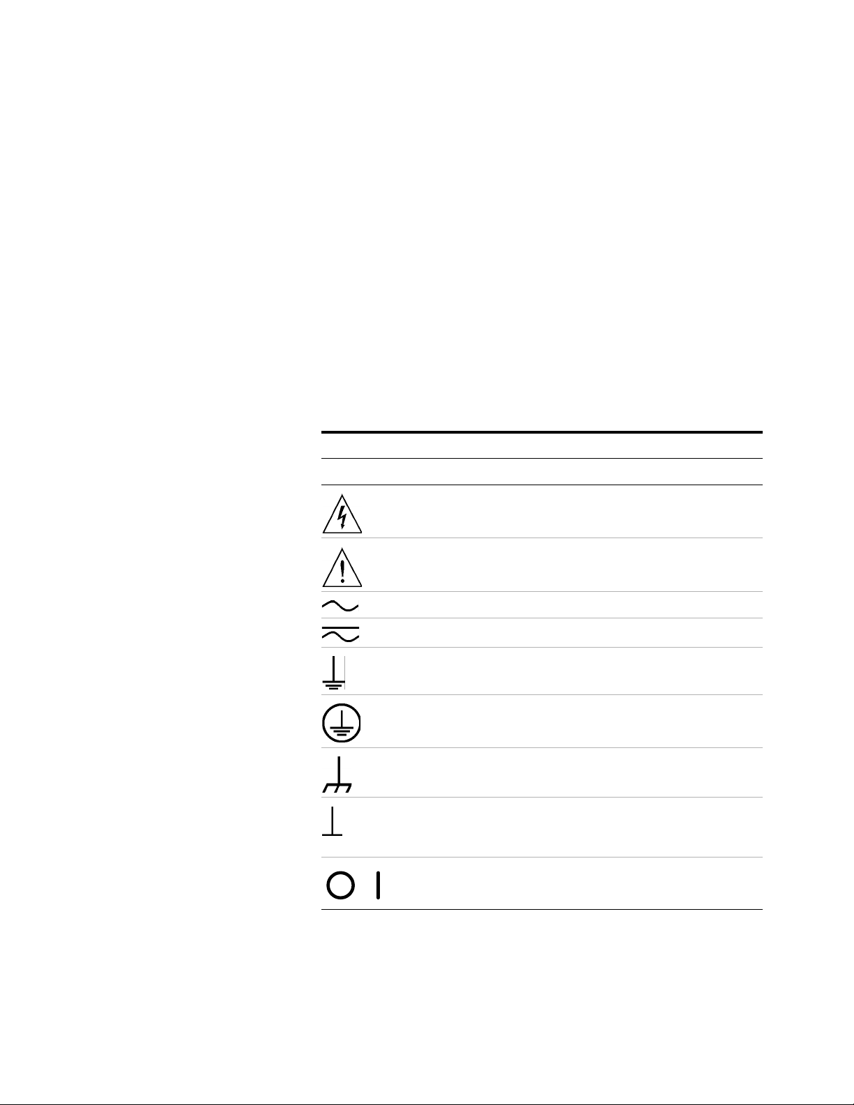
Symbols and markings on the system, in manuals and on
instruments alert you to potential risks, provide information
about conditions, and comply with international regulations.
Table 2-2 defines the symbols and markings you may find in a
manual or on an instrument.
Table 2-2 Safety Symbols and Regulatory Markings
Symbols Description
Safety symbols
Warning: risk of electric shock.
Caution: refer to accompanying documents.
Alternating current.
Both direct and alternating current.
Earth (ground) terminal
Protective earth (ground) terminal
Frame or chassis terminal
Terminal is at earth potential. Used for measurement and
control circuits designed to be operated with one terminal at
earth potential.
Switch setting indicator. O = Off, | = On.
2-6 E6198B/E6218A Switch/Load Unit User Manual
Page 27
Safety and Regulatory Information 2
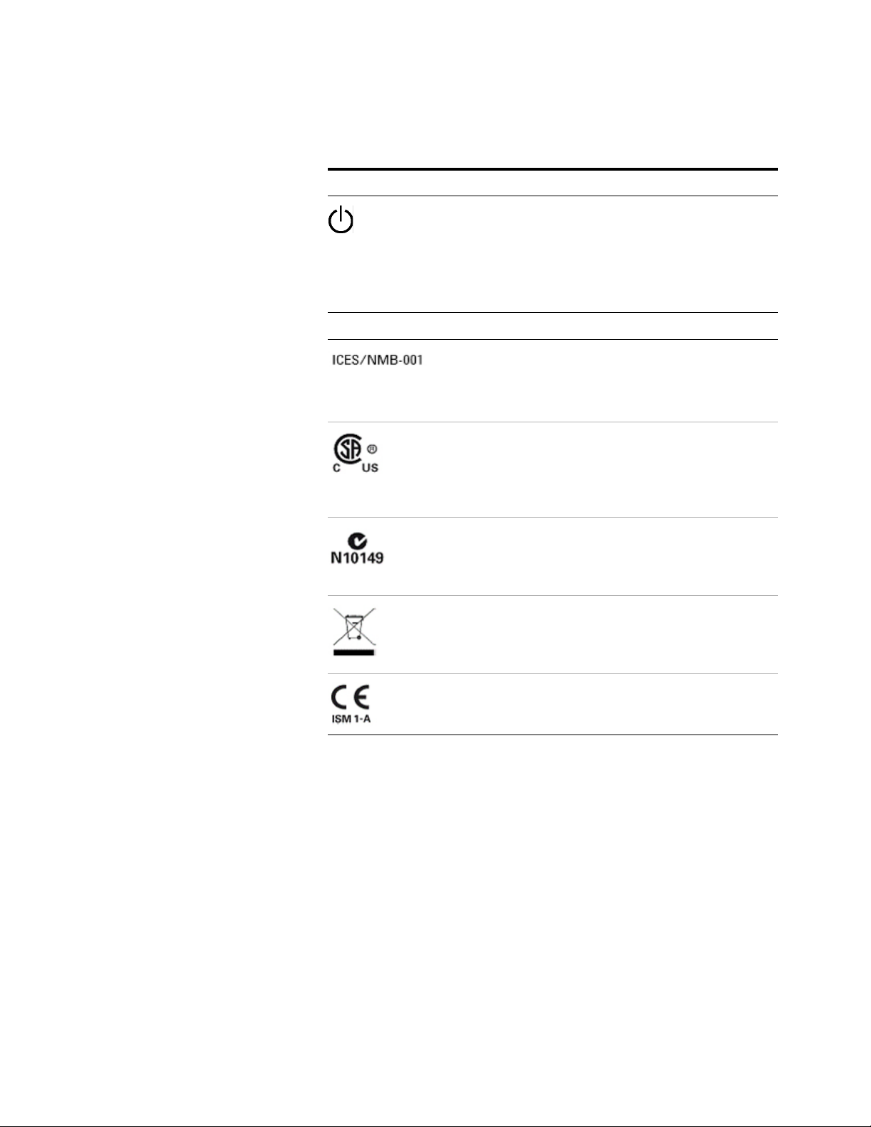
Table 2-2 Safety Symbols and Regulatory Markings (continued)
Symbols Description
Standby (supply); units with this symbol are not completely
disconnected from ac mains when this switch is off. To
completely disconnect the unit from ac mains, either
disconnect the power cord, or have a qualified electrician
install an external switch.
Regulatory markings
This text indicates that the ISM device complies with
Canadian ICES-001.
Cet appareil ISM est conforme à la norme NMB-001 du
Canada.
The CSA mark is a registered trademark of the Canadian
Standards Association. A CSA mark with the indicators “C”
and “US” means that the product is certified for both the
U.S. and Canadian markets, to the applicable American and
Canadian standards.
The C-tick mark is a registered trademark of the Spectrum
Management Agency of Australia. This signifies compliance
with the Australia EMC Framework regulations under the
terms of the Radio Communication Act of 1992.
This instrument complies with the WEEE Directive
(2002/96/EC) marking requirement. This affixed product
label indicates that you must not discard this
electrical/electronic product in domestic household waste.
The CE mark is a registered trademark of the European
Community. This CE mark shows that the product complies
with all the relevant European Legal Directives.
E6198B/E6218A Switch/Load Unit User Manual 2-7
Page 28
2 Safety and Regulatory Information
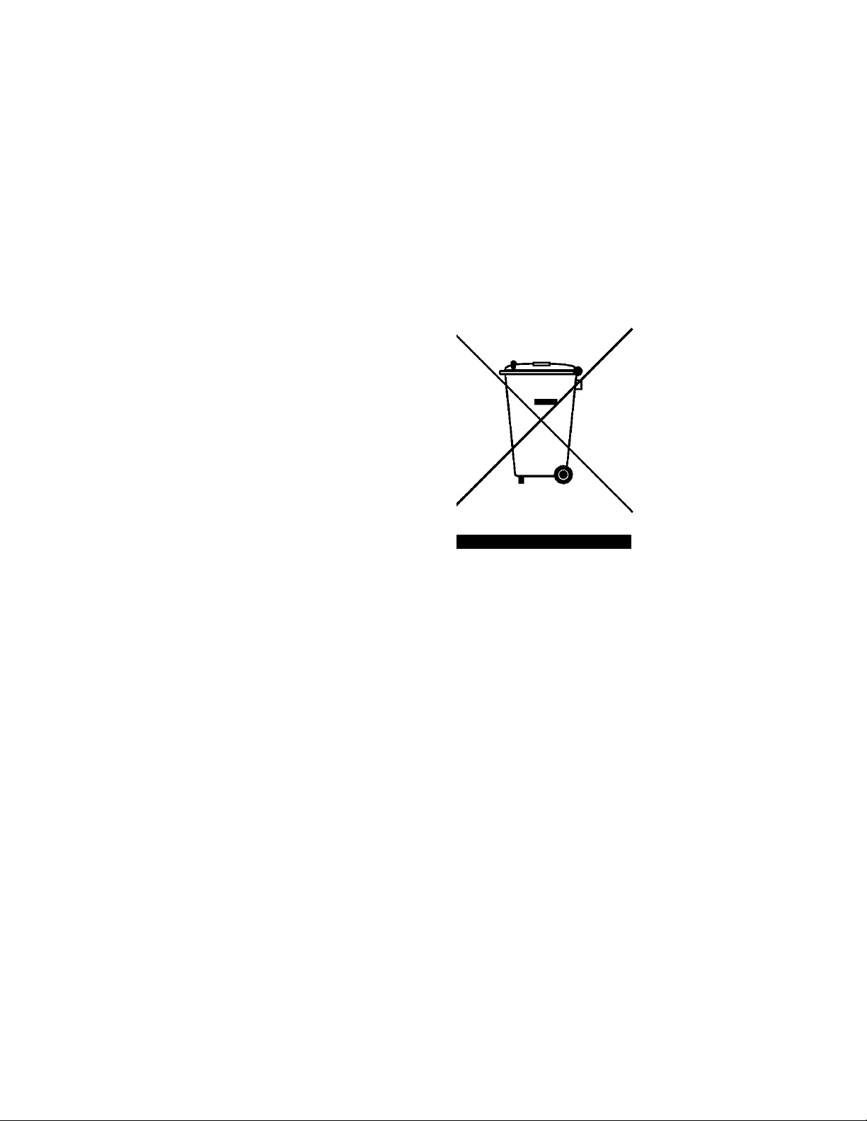
End of Life: Waste Electrical and Electronic Equipment (WEEE) Directive 2002/96/EC
This product complies with the WEEE Directive (2002/96/EC)
marking requirement. The affixed product label (see below)
indicates that you must not discard this electrical/electronic
product in domestic household waste.
Product Category:
With reference to the equipment types in the WEEE directive
Annex 1, this product is classified as a “Monitoring and Control
Instrumentation” product.
Do not dispose in domestic household waste
To return unwanted products, contact your local Agilent office,
or see:
http://www.agilent.com/environment/product
for more information.
2-8 E6198B/E6218A Switch/Load Unit User Manual
Page 29

Agilent TS-5000
E6198B Switch/Load Unit User Manual
3
Switch/Load Unit and Plug-In Cards
E6198B Standalone/Integrated Switch/Load Unit Rating 3-2
E6198B Standalone Switch/Load Unit Description 3-3
E6198B Integrated Switch/Load Unit Description 3-9
Backplane And Breakout Board Connectors and LEDs 3-10
Differentiating E6198B Standalone Option and System Integrated
Option 3-22
This chapter gives an overview of the Agilent E6198B
(Standalone and Integrated) Switch/Load Unit (SLU), load
cards, and other associated equipment.
Agilent Technologies
3-1
Page 30

3 Switch/Load Unit and Plug-In Cards
E6198B Standalone/Integrated Switch/Load Unit Rating
Electrical
Tab le 3- 1 Switch/Load Unit Rating (Electrical)
Parameter Value
Input Voltage 100–240 VAC nominal
Frequency 50/60 Hz
Power 325 W maximum
Mechanical
Tab le 3- 2 Switch/Load Unit Rating (Mechanical)
Parameter Value
Width 484.64 mm
Height 373.61 mm
Depth 520.52 mm
Weight 15.0 kg
3-2 E6198B/E6218A Switch/Load Unit User Manual
Page 31

Switch/Load Unit and Plug-In Cards 3
E6198B Standalone Switch/Load Unit Description
The Switch/Load Unit (Figure 3-1) consists of a standard VME
type enclosure, a custom high current backplane, and slots for
up to 21 optional Agilent plug-in cards. The following plug-in
cards are available:
• Agilent E6175A 8-channel load card
• Agilent E6176A 16-channel load card
• Agilent E6177A 24-channel load card
• Agilent U7177A 24-channel load card with current sense
• Agilent E6178B 8-channel heavy duty load card
• Agilent N9377A 16-channel dual-load load card
• Agilent N9378A 24-channel low resistance load card
• Agilent N9379A 48-channel high-density load card
• Agilent E8792A 32-pin matrix card with instrumentation
support
• Agilent E8793A 32-pin matrix card
• Agilent E8782A 40-pin matrix card with 24 instrumentation
support
• Agilent E8783A 64-pin matrix card
• Agilent E8794A custom card
• Agilent U7178A 8-channel heavy duty load card
• Agilent U7179A 16-channel high current load card
Load cards are described in detail in Chapter 5 and Appendix A
to Appendix C of this manual. The pin matrix cards are
described in Chapter 6. The E8794A custom card is discussed in
Chapter 7.
E6198B/E6218A Switch/Load Unit User Manual 3-3
Page 32

3 Switch/Load Unit and Plug-In Cards
Figure 3-1 Agilent E6198B Standalone Switch/Load Unit Front View
Figure 3-2 Agilent E6198B Standalone Switch/Load Unit Back View
3-4 E6198B/E6218A Switch/Load Unit User Manual
Page 33

USB Interface
Switch/Load Unit and Plug-In Cards 3
In addition to holding load cards, pin matrix cards, and custom
cards, the Switch/Load Unit also provides the following
capabilities:
• Built-in USB interface
• Digital I/O
• Current Sense
• Power Bus Sense
• Two DAC Channels
• +5, +12V, –12V, and Spare Power
Each of the above features is described in detail in the following
sections.
The Switch/Load Unit switching and data transfer is controlled
by a built-in USB interface. Figure 4-13 shows the location of
the USB interface.
Digital I/O
Digital Input
The Switch/Load Unit provides 8-bits of digital input, 8-bits of
digital output (Open Drain Out), and 8-bits of TTL-level digital
output (Spare Digital Out). There is no handshaking capability
in the digital I/O. Typical usage of the digital I/O includes:
• Automation control
• Digital control of circuitry on the Agilent E8794A Custom
Card
• Digital switches (for example, to indicate door open/closed)
• Actuator control
• Fixture ID
The digital input bits have TTL thresholds (0.55 Vdc for low,
3.0 Vdc for high) and are protected to ±24 Vdc. These includes
the Fixture IDs that also use standard TTL inputs, but are not
protected to ±24 Vdc. Figure 3-3 is a typical example showing
the usage of a digital input bit.
E6198B/E6218A Switch/Load Unit User Manual 3-5
Page 34

3 Switch/Load Unit and Plug-In Cards
Open Drain Digital Output
Figure 3-3 Digital Input Example
The digital output bits use open drain drive circuitry designed
for pull-ups up to +24 Vdc. The output port FET can sink up to
250 mA. Figure 3-4 shows one digital output bit controlling a
relay.
Figure 3-4 Digital Output Example
3-6 E6198B/E6218A Switch/Load Unit User Manual
Page 35

DAC Channels
NOTE
The two 14-bit channels of DAC provide ±16 V at 10 mA each. To
provide this voltage swing, a charge pump is used to step-up the
±12 V supply. The DAC channels are typically used for
controlling differential input, voltage-controlled power supplies.
+5 Vdc, +12 Vdc, –12 Vdc, Spare Power
+5 V, +12 V, and –12V from the Switch/Load Unit Power Supply.
The +5 V supply can deliver 7.5 A to 30 A, +12 V supply can
deliver 2.5 A to 12.5 A, and the –12 V supply can deliver 700 mA
to 1 A. You can also connect an additional (spare) power supply
to the Switch/Load Unit backplane, see “Connecting an
Additional (Spare) Power Supply for details.
Power supplies +5 V, +12 V, and –12 V for E6198B have non-resettable
fuses. (Non-resettable fuses need to be replaced, refer to Table 3-11 for
fuse ratings.)
Switch/Load Unit and Plug-In Cards 3
Spare supply has resettable fuse. If an overload occurs, the fuse(s) open.
To reset the fuse(s), remove power from the Switch/Load Unit for
approximately 20 seconds. The fuse(s) reset when power is re-applied.
Current Sense
The Isense+ and Isense– lines sense current on a selected load
card channel. They connect to the current sense bus on the SLU
backplane. Current sense lines of each channel are multiplexed.
Only one channel can connect to the current sense bus at one
time.
Power Bus Sense
Power Bus Sense lines 1-4 remotely sense power supplies
connected to power buses 1-4. This sensing compensates the
losses in the system wiring to ensure that the set voltage is
applied to the sense point.
Switch/Load Unit Block Diagram
Figure 3-5 shows a block diagram of the SLU. All plug-in cards
are optional so your system will have a different mix of cards
from that shown here. The Test System Interface or Mass
Interconnect are also optional — you can also interface directly
to the Switch/Load Unit. See Chapter 4 for details.
E6198B/E6218A Switch/Load Unit User Manual 3-7
Page 36

3 Switch/Load Unit and Plug-In Cards
Load Card #2
Pin Matrix Card #2
Load Card #1
Pin Matrix Card #1
Custom Card
Agilent E6198B Switch/Load Unit
Load Card #n
Pin Matrix Card #n
Digital In, Power Bus Sense ,
Isense
Switch/Load Unit
Circuitry
Digital Out, DAC, +12 V, -12V
Power Bus
Power
Supply #1
Power
Supply #2
Power
Supply #3
An alog B us
Test System Interface or Mass Interconnect
Note : All plug -in car ds are opti onal - -the m ix and numbers of car ds in your system w i l l be di ffer ent than shown here .
To/From
UUT
Figure 3-5 Switch/Load Unit Block Diagram
3-8 E6198B/E6218A Switch/Load Unit User Manual
Page 37

E6198B Integrated Switch/Load Unit Description
Sense Bussed/Split PB Sense Remote/Local Frame SelectSense Bussed/Split
The Agilent E6198B now comes as a system integrated unit or
as a standalone unit. The features and functionality remains the
same as the previous E6198A. Differences between the two are
in the cabling and function selection panel.
Figure 3-6 E6198B Integrated SLU Back View
Switch/Load Unit and Plug-In Cards 3
E6198B/E6218A Switch/Load Unit User Manual 3-9
Page 38

3 Switch/Load Unit and Plug-In Cards
BACKPLANE SLU
T4 T8 T9 T1 T5 T10 T11 T2 T6 T12 T13 T3 T7 T14
J102
J101
J1
J3
J2
J803
J801
J802
1
2
14
13
1
214
13
1
2
14
13
1
3
94
96
1
3
94
96
J201
J202J203
J204
J205
J206J207
J208J209
J210J211
J212
J213
J214J215
J216
J217
J218J219
J220
J221
J104
J111 J110
J109
J106 J107
J105 J108
Backplane And Breakout Board Connectors and LEDs
Figure 3-7 Switch/Load Unit Backplane Connectors (USB port adaptor board Not Shown)
3-10 E6198B/E6218A Switch/Load Unit User Manual
Page 39

Switch/Load Unit and Plug-In Cards 3
BREAKOUT BOARD (External Board)
BACK
J_5
J_6
J_7
J_3
FRONT
J_1
J_8
S3A-S3F
S1A-S1D
S2A-S2H
Figure 3-7 shows the locations of the various backplane
connectors and LEDs. These components are described on the
following pages. See Table 3-3 for more detail.
Figure 3-8 Switch/Load Unit Breakout Board Connectors (Standalone
only)
Figure 3-8 shows connector locations on the breakout board
(external board). Refer Table 3-5 for the detailed descriptions.
The breakout panel is available with the E6198B Standalone
option and is easily accessible from the SLU rear.
E6198B/E6218A Switch/Load Unit User Manual 3-11
Page 40

3 Switch/Load Unit and Plug-In Cards
Backplane Connector Name
Table 3-3 lists the connectors on a E6198B backplane.
Tab le 3- 3 Backplane Connectors for E6198B
E6198B Reference
Designator
J2 SLU Current Sense: Bussed/Split
J3 SLU Power Bus Sense Select: Local/Remote
J1 Frame Select
T1-T14 SLU Logic Power Supply Connector
J101 To USB Controller Connector
J102 Utility Connector
J104 External Reset (reserved)
J105 +5 V Indicator (+5 V Status)
J106 +12 V Indicator (+12 V Status)
J107 –12 V Indicator (–12 V Status)
J108 READY Indicator (Control Status)
J109 +12 V Output For Fan
J110 +12 V Output For Fan
J111 +12 V Output For Fan
J201-J221 Load Card Slots Connector
Description
J801 & J802 Power Busses PB1-PB4
J803 Sense For PB1-PB4
3-12 E6198B/E6218A Switch/Load Unit User Manual
Page 41

Backplane J1, J2 and J3 Connectors
Table 3-4 shows the factory default configuration for the
backplane connectors.
Tab le 3- 4 Backplane Factory Default Connector Settings
Switch/Load Unit and Plug-In Cards 3
Connector
J1 0 (Zero)
J2 Bussed Switch/Load Unit Current-Sense Bus
J3 Local
Default
Setting
Description
Frame Select address 0-7. When using multiple
Switch/Load Units in your test system, Connector
J1 provides a unique address for each
Switch/Load Unit. Factory default (one
Switch/Load Unit) is 0.
Switch/Load Unit Power Bus Sense select:
Local/Remote
E6198B/E6218A Switch/Load Unit User Manual 3-13
Page 42

3 Switch/Load Unit and Plug-In Cards
NOTE
Breakout Board Connector Name (for E6198B Standalone option)
Breakout board extends the connection from backplane to SLU
rear. Table 3-5 lists the description of each connector.
Tab le 3- 5 Breakout Board Connectors
Connector Description
J_1 Utility Connector (J102 extension connector)
J_3 Utility Connector (J102 internal connector)
J_5
J_6
J_7
J_8 Spare Supply Connector
S1A-S1D Toggle switches for Local/Remote
S2A-S2H Toggle switches for Frame Select
S3A-S3F Toggle switches for Isense Bussed/Split
The breakout board is not available with E6198B System Integrated
Frame Select & Spare Supply (Connect to J1 of
backplane internal connector)
Power Bus Sense Local/Remote (Connect to J3 of
backplane internal connector)
Isense Bussed/Split (Connect to J2 of backplane
internal connector)
option. See Figure 3-6.
3-14 E6198B/E6218A Switch/Load Unit User Manual
Page 43

Backplane Connectors
The following connector descriptions are referenced to
Figure 3-9.
T1-T14 are the Switch/Load Unit power supply connectors.
The supply provides the required +5 V and ±12 V for
powering the backplane and Load Cards. These power supply
lines are protected by fuses.
J102 connects the signals that are cabled between the
Switch/Load Unit and the mass interconnect. These signals
include:
Eight-bit fixture ID pins allow the user to configure a
unique ID for each mass interconnect fixture and read it
back. Address 0 of the backplane is used for the fixture ID
and to read back the status of reset and busy state of the
backplane.
Switch/Load Unit and Plug-In Cards 3
Digital In/Digital Out eight bits each (TTL level).
Open Drain Outputs eight bits each.
Four pairs of current sense busses correspond to the
current sense pairs from slots 1-5, 6-10, 11-15, and 16-21.
These busses may be connected together to form a single bus,
or split into independent current sense busses using jumpers
on SLU backplane J2 connector (Integrated) or switches
S3A-S3F on breakout board (Standalone). Factory default
connects all sense busses to a single bus. Find more
information on when should you split the busses and how in
Chapter 3.
Four remote power bus sense pins remotely sense the
power busses at the UUT. Remote or local sensing for power
bus PB1-PB4 can be set using jumpers on SLU backplane J3
connector or S1A-S1D on breakout board (Standalone).
Factory default is remote sense.
DAC 1 and DAC 2 outputs.
J201-J221 are the slot connectors for Pin Matrix Card or
Load Card, slots 1-21 respectively. The top half of each slot
connector is used to provide slot power, address, data, and
control lines. The bottom half of each connector is used to
connect the power busses to the Load Cards.
E6198B/E6218A Switch/Load Unit User Manual 3-15
Page 44

3 Switch/Load Unit and Plug-In Cards
Backplane LEDs
J801 and J802 provide the high power connections to power
busses PB1-PB4. Three supplies with a common connection
to PB1 or two independent supplies can be configured on the
four power busses. Bulk bypassing between power busses
may be desirable in certain applications.
J803 provides the sense connections for the four power
busses.
Two sets of LEDs are provided on the backplane for a visual
indication that the Switch/Load Unit is functioning:
Power LEDs. The +5V, +12V and –12V LEDs indicate the status
of the corresponding voltage lines from the Switch/Load Unit
power supply and READY LED indicate the status of SLU ready
to operate. If one or more LEDs is NOT illuminated, the most
likely problem was an overcurrent situation that opened the
non-resettable fuse(s). To change fuse(s), remove power from
the Switch/Load Unit for approximately 20 seconds. The fuse(s)
will reset when power is re-applied. (Non-resettable fuses need
to be replaced rather than power off to reset, refer to Table 3-11
for fuse ratings.)
Frame LEDs. The Frame Access LED flashes to indicate a data
access has occurred to that Switch/Load Unit. The five Slot
Address LEDs indicate the slot currently being addressed.
J102 Pinouts
Switch/Load Unit backplane connector J102 carries signals
such as the Digital I/O, DAC 1 and 2, and ISense (current sense)
lines. When configured as part of a standard Agilent system,
J102 of the Switch/Load Unit is connected via cable to a mass
interconnect panel. User connections to the UUT are then made
from the mass interconnect panel. Refer to the appropriate
mass interconnect wiring guide for connection details.
You can also make connections directly to J102 or to the
exposed end of an Agilent E3750-61607, Agilent E6170-61610,
or Agilent E6198-61625 cable connected to J102. Figure 3-9 is a
J102 connector pinout and Figure 3-10 shows the pinouts for
the exposed cable connector end. Table 3-6 defines the signals
available on J102.
3-16 E6198B/E6218A Switch/Load Unit User Manual
Page 45

Figure 3-9 Switch/Load Unit J102 Connector Pinouts
Open Drain Out (7)
Open Drain Out (5)
Open Drain Out (1)
Open Drain Out (3)
Open Drain Out (6)
Open Drain Out (2)
Open Drain Out (0)
Open Drain Out (4)
DAC2
DAC1
No Connection
System Gnd
System Gnd
Spare Supply
+12 Vdc Supply
+12 Vdc Supply
Power Bus Sense 4
Power Bus Sense 2
ISense+ (4)
ISense+ (3)
ISense+ (2)
ISense+ (1)
Spare_DigOut (7)
Spare_DigOut (5)
Spare_DigOut (3)
Spare_DigOut (1)
Digital In (7)
Digital In (5)
Digital In (3)
Digital In (1)
System Gnd
Fixture ID (7)
Fixture ID (5)
Fixture ID (3)
Fixture ID (1)
System Gnd System Gnd
Fixture ID (0)
Fixture ID (2)
Fixture ID (4)
Fixture ID (6)
System Gnd
Digital In (0)
Digital In (2)
Digital In (4)
Digital In (6)
Spare_DigOut (0)
Spare_DigOut (6)
Spare_DigOut (4)
Spare_DigOut (2)
ISense- (1)
ISense- (4)
ISense- (3)
ISense- (2)
Power Bus Sense 1
Power Bus Sense 3
System Gnd
System Gnd
System Gnd
System Gnd
No Connection
-12 Vdc Supply
+12 Vdc Supply
+12 Vdc Supply
96
94
93 90
91 888785
84 81
82 79
78
76
75 72
73 706967
66 63
64 61
60
58
57 54
55 525149
48 45
46 43
42
40
39 36
37 343331
30 27
28 25
24 21
22 19
18
16
15 12
13 1097
63
41
NC NC NC NC NC NC NC NC NC NC NC NC NC NC NC NC NC NC NC NC NC NC NC NC NC NC NC NC NC NC NC NC
A
B
C
Row 1
Row 2
Row 3
Row 4
Row 5
Row 6
Row 7
Row 8
Row 9
Row 10
Row 11
Row 12
Row 13
Row 14
Row 15
Row 16
Row 17
Row 18
Row 19
Row 20
Row 21
Row 22
Row 23
Row 24
Row 25
Row 26
Row 27
Row 28
Row 29
Row 30
Row 31
Row 32
NOTE
Switch/Load Unit and Plug-In Cards 3
For E6198B Standalone option, connector J102 is extended from the
backplane to the breakout board. See Figure 3-8.
E6198B/E6218A Switch/Load Unit User Manual 3-17
Page 46

6 4
9 7
12 10
15 13
18 16
21 19
27 25
30 28
33 31
36 34
39 37
42 40
45 43
51 49
53 52
57 55
60 58
63 61
66 64
69 67
1
Open Drain Out (6)
Open Drain Out (2)
Open Drain Out (0)
Open Drain Out (4)
System Gnd
Fixture ID (0)
Fixture ID (2)
Fixture ID (4)
Fixture ID (6)
System Gnd
Digital In (0)
Digital In (2)
Digital In (4)
Digital In (6)
Spare_DigOut (0)
Spare_DigOut (6)
Spare_DigOut (4)
Spare_DigOut (2)
ISense- (1)
ISense- (4)
ISense- (3)
ISense- (2)
Power Bus Sense 1
Power Bus Sense 3
System Gnd
System Gnd
System Gnd
System Gnd
No Connection
-12 Vdc Supply
+12 Vdc Supply
+12 Vdc Supply
3
Open Drain Out (7)
Open Drain Out (5)
Open Drain Out (1)
Open Drain Out (3)
DAC2
DAC1
No Connection
System Gnd
System Gnd
Spare Supply
+12 Vdc Supply
+12 Vdc Supply
Power Bus Sense 4
Power Bus Sense 2
ISense+ (4)
ISense+ (3)
ISense+ (2)
ISense+ (1)
Spare_DigOut (7)
Spare_DigOut (5)
Spare_DigOut (3)
Spare_DigOut (1)
Digital In (7)
Digital In (5)
Digital In (3)
Digital In (1)
System Gnd
Fixture ID (7)
Fixture ID (5)
Fixture ID (3)
Fixture ID (1)
System Gnd
75 73
78 76
81 79
84 82
87 85
90 88
93 91
24 22
48 46
72 70
96 94
ABC
Cable Connector Endand Front View
(Center Column Not Used)
Row 24
Row 23
Row 21
Row 22
Row 32
Row 31
Row 30
Row 29
Row 28
Row 27
Row 26
Row 25
Row 20
Row 19
Row 18
Row 17
Row 16
Row 15
Row 14
Row 13
Row 12
Row 11
Row 10
Row 9
Row 8
Row 7
Row 6
Row 5
Row 4
Row 3
Row 2
Row 1
3 Switch/Load Unit and Plug-In Cards
Figure 3-10 Cable Connector Pinouts
3-18 E6198B/E6218A Switch/Load Unit User Manual
Page 47

Tab le 3- 6 J102 signal definitions
Switch/Load Unit and Plug-In Cards 3
+12Vdc, –12Vdc
Supply
Spare Supply Connection for a user installed power supply not included in the standard system. Refer
DAC1
DAC2
Digital In 0 - 7
Open Drain Out 0 - 7
Spare_DigOut
Fixture ID (0 - 7) The Fixture ID lets you configure a unique ID for each mass interconnect fixture and
Isense+ (1 - 4)
Isense– (1 - 4)
+12V and –12V from the Switch/Load Unit Power Supply. The +12V supply can deliver
12.5A, the –12V supply can deliver 2.1A.
to “Connecting an Additional (Spare) Power Supply" for details.
The Switch/Load Unit provides two 14-bit channels of DAC which supply ±16 V at 10 mA
each.
The Switch/Load Unit provides 8-bits of digital input, 8-bits of open drain digital output,
and 8-bits of TTL-level digital output (Spare_DigOut). There is no handshaking
capability.
read it back. ID sent as TTL level bits.
These lines connect to the current sense bus on the Switch/Load Unit backplane. These
lines are used for sensing current on a selected load card channel. The 8-channel and
16-channel load cards are designed to connect to the current sense bus. Each load card
channel’s current sense lines are multiplexed so that on each card only one channel at a
time can be connected to the current sense bus. The current sense lines and the slots
they connect to are:
Isense lines (1) connect to Switch/Load Unit slots 1 - 5.
Isense lines (2) connect to Switch/Load Unit slots 6 - 10.
Isense lines (3) connect to Switch/Load Unit slots 11 - 15.
Isense lines (4) connect to Switch/Load Unit slots 16 - 21.
Two or more sets of the above lines can be bussed together select from toggle switches.
Refer to page 12 for details.
Power Bus Sense 1 - 4 The remote sense lines for the power supplies connected to power buses 1 - 4.
Gnd Chassis ground of the Switch/Load Unit.
E6198B/E6218A Switch/Load Unit User Manual 3-19
Page 48

3 Switch/Load Unit and Plug-In Cards
J1 Pinout
Tab le 3- 7 Switch/Load Unit J1 Pinout
FS1 FS3 FS5 FS7 NC GND SS
FS0 FS2 FS4 FS6 FRAME GND SS
J2 Pinout
Table 3-7 shows pinout of J1 Frame Select & Spare Supply (SS).
Frame 0 is selected if FS0 and FRAME are both are connected;
Frame 1 is selected if FS1 and FRAME are both are connected,
and so on. Default setting is frame 0 (zero). More detail about SS
(Spare Supply), please refer “Connecting an Additional (Spare)
Power Supply" .
Table 3-8 show pinouts of J2 ISENSE Bussed/Split. Default
setting for J2 is ISENSE Bussed.
Tab le 3- 8 Switch/Load Unit J2 Pinout
J3 Pinout
Tab le 3- 9 Switch/Load Unit J3 Pinout
IS(-2) IS(+2) IS(-3) IS(+3) IS(-4) IS(+4) NC
IS(-1) IS(+1) IS(-2) IS(+2) IS(-3) IS(+3) NC
Table 3-9 shows pinouts of Power Bus Sense Local/Remote.
Local 1 is selected if LOC_S1 is connected with PB1; Remote 1 is
selected if REM_S1 is connected with PB1, and so on. Default
setting for J3 is Local.
LOC_S1 PB2 REM_S2 LOC_S3 PB4 REM_S4 LOC_S1
PB1 REM_S1 LOC_S2 PB3 REM_S3 LOC_S4 PB1
3-20 E6198B/E6218A Switch/Load Unit User Manual
Page 49

T1-T14 SLU Logic Power Supply Connector
T1-T14 provides the required +5 V and ±12 V for powering the
backplane and Load Cards. Table 3-10 lists each jumper and its
corresponding input voltage.
Table 3-10 Power Supply Input for each Jumpers
Jumper Input Voltage
T1 +5 V
T2 +5 V
T3 +5 V
T4 –12 V
T5 +12 V
T6 +12 V
T7 +12 V
Switch/Load Unit and Plug-In Cards 3
T8 GND
T9 GND
T10 GND
T11 GND
T12 GND
T13 GND
T14 GND
E6198B/E6218A Switch/Load Unit User Manual 3-21
Page 50

3 Switch/Load Unit and Plug-In Cards
Differentiating E6198B Standalone Option and System Integrated Option
The key differences between the standalone and system
integrated option can be found at the SLU rear cover.
On a standalone unit, the backplane connectors are extended to
the breakout board attached to the SLU rear cover. At the SLU
rear, you will find toggle switches for SLU configuration, and
power and sense buses connectors protected by a cable
enclosure. (See Figure 3-11.)
On a system integrated unit, you will find cut-outs on the SLU
rear cover to allow cable routing from the SLU backplane.
Jumpers are used for SLU configuration.
Figure 3-11 Switch/Load Unit Rear View (Standalone Option)
3-22 E6198B/E6218A Switch/Load Unit User Manual
Page 51

Figure 3-12 Switch/Load Unit Rear View (System Integrated Option)
Switch/Load Unit and Plug-In Cards 3
E6198B/E6218A Switch/Load Unit User Manual 3-23
Page 52

3 Switch/Load Unit and Plug-In Cards
Fuse Ratings
Fuses are incorporated inside E6198B Switch/Load Unit. There
are 10 fuses and 7 fuses for Standalone SLU and Integrated SLU
respectively. Please refer Table 3-11 for more detail.
Table 3-11 Fuses Ratings
Standalone Integrated Description
Fuse1 Fuse1 1 A, –12 V
Fuse2 Fuse2 6 A, +12 V_1
Fuse3 Fuse3 6 A, +12 V_2
Fuse4 Fuse4 Not Used
Fuse5 Fuse5 15 A, +5 V_1
Fuse6 Fuse6 15 A, +5 V_2
Fuse7 Fuse7 Not Used
Fuse8 - 30 A, PB2
Fuse9 - 30 A, PB3
Fuse10 - 30 A, PB4
DC Power Bus Connections
PB1 to PB4 are the DC power bus connections as seen in
Figure 3-11 for the standalone unit. Notice the protective cable
enclosure covering both the power bus cabling and power sense
cabling for better protection.
For the integrated unit, there is no protective cable enclosure,
and you will need to configure the cabling directly onto the
backplane, behind the SLU backcover.
3-24 E6198B/E6218A Switch/Load Unit User Manual
Page 53

Agilent TS-5000
WARNING
CAUTION
E6198B Switch/Load Unit User Manual
4
Configuring the Switch/Load Unit
Card Location Recommendations 4-2
Connecting an Additional (Spare) Power Supply 4-5
Configuring the Power Busses 4-6
Connecting E6198B to the Computer via USB Interface or Parallel
Port 4-12
Adding a Second Switch/Load Unit 4-13
Load Box Installation 4-14
This chapter shows you how to configure the Switch/Load Unit.
SHOCK HAZARD. Only service-trained personnel who are aware
of the hazards involved should install, remove, or configure the
Switch/Load Unit or plug-in cards. Before you remove any
installed card, disconnect AC power from the mainframe and from
other cards that may be connected to the cards.
STATIC ELECTRICITY
Static electricity is a major cause of component failure. To prevent
damage to electrical components, observe anti-static techniques
whenever installing or removing a card in the Switch/Load Unit or
whenever working on a card.
Agilent Technologies
4-1
Page 54

4 Configuring the Switch/Load Unit
Card Location Recommendations
Slot 1 to 21 of a Switch/Load Unit are identical and able to take
any supported Pin Matrix or Load Cards. This sections provides
an example on card installation guideline to maintain
consistency between test systems. Your test system may use a
different guideline that fits your application.
For a single Agilent E6198B Switch/Load Unit installed in the system
Install matrix cards first. Slots 15 through 21 are reserved for
the matrix and custom modules. Starting from slot 21 and
working down, install matrix modules and custom modules in
the following order:
• Agilent Pin Matrix and Instrument Multiplexer Card
(E8792A or E8782A)
• Agilent Pin Matrix Card(s) (E8793A and/or E8783A)
• Agilent E8794A Custom Card(s)
Install the load cards using the following rules:
• Agilent N9379A 48-Channel Load Cards
Install any N9379A cards first, starting at slot #1.
• Agilent E6177A 24-Channel Load Cards
Install any E6177A cards next.
• Agilent U7177A 24-Channel Load Cards with Current
Sense
Install any U7177A cards next.
• Agilent N9378A 24-Channel Load Cards
Install any N9378A cards next. To allow for future expansion,
leave an open slot after the last N9378A card.
• Agilent E6176A 16-Channel Load Cards
Install any Agilent E6176A cards next.
• Agilent N9377A 16-Channel Load Cards
Install any Agilent N9377A cards next. To allow for future
expansion, leave an open slot after the last N9377A card.
• Agilent E6178B 8-Channel Heavy Duty Load Cards
Agilent E6178B 8 channel Heavy Duty cards require two slots
each. These cards are installed in even slot locations only.
Install E6178B cards starting with the first available even
slot following the 16 channel cards.
4-2 E6198B/E6218A Switch/Load Unit User Manual
Page 55

Configuring the Switch/Load Unit 4
CAUTION
Slot:
E8792A 32-Pin
Matrix and
Instrument
Multiplexer
Card
E6175A
8-Channel
Agilent E6176A
16-Channel
Load Cards
N9379A
48-Channel
Switch/Load Unit Slot Front View
Agilent E8794A
Custom Card
Empty
E6177A
24-Channel
Empty
N9378A
24-Channel
Empty
Empty
Empty
N9378A
24-Channel
Empty
1 2 3
4 5 6
7 8 9
10
11 12
13
14 15
16
17 18 19
20 21
• Agilent E6175A 8-Channel Load Cards
Agilent E6175A 8 channel cards require two slots each.
These cards are installed in even slot locations only. Install
E6175A cards in first available even slot following the
E6178B 8-Channel Heavy Duty cards.
Please close the gap for rear side of the connector if using own
fabricated cable with connector.
For example, Figure 4-1 shows the standard locations for matrix
and load cards for a system which contains three matrix cards,
a custom card, two 24 channel, four 16 channel, one 8 channel,
and one 8 channel heavy duty load card. If using this
configuration, be sure to leave the slots open between the cards,
as shown in the figure.
Figure 4-1 Example of Load/Matrix/Custom Cards Loading Order
E6198B/E6218A Switch/Load Unit User Manual 4-3
Page 56

4 Configuring the Switch/Load Unit
Load Card Types and IDS
Each card is assigned a different type and has a 10-pin
connector that lets you assign a unique binary code ID number
to each card. See“Load Card Type and Configuration ID" for
more information.
4-4 E6198B/E6218A Switch/Load Unit User Manual
Page 57

Configuring the Switch/Load Unit 4
C507
100uF
50V
HP 0180-3334
RT505
700m
HP 0837-0440
J1
+
Raytheon P/N
SMD100 or
equivalent
V+24V
To J102
J1
1
2
14
13
SS ( +ve Polarity)
Connecting an Additional (Spare) Power Supply
The Spare Supply pinout located at SLU backplane connector J1
(Integrated) allows you to add an additional power supply such
as a +24 V power supply for powering higher voltage relays. It is
necessary to remove the SLU rear cover to access this
connector. Figure 4-2 shows the placement and orientation on
the backplane for the power supply components. Both
Connector J1 and Capacitor C507 are loaded at the factory.
Capacitor C507 is to minimize high-frequency noise on the
supply line. The auxiliary supply output (Spare Supply) appears
on Switch/Load Unit connector J102 pin 79.
Figure 4-2 Component Location/Schematic for User-Installed External Power Supply
For SLU Standalone option, you can connect to the Spare
Supply Input directly from SLU rear. See Figure 4-3.
Figure 4-3 Spare Supply (Input) Connector on SLU rear (SLU standalone)
E6198B/E6218A Switch/Load Unit User Manual 4-5
Page 58

4 Configuring the Switch/Load Unit
J801 J802
PB1 PB2 PB3 PB4
PC Board Traces
Configuring the Power Busses
The UUT power supplies are connected to the power busses
PB1-PB4. Figure 4-4 shows the power bus connectors J801 and
J802 located on the Switch/Load Unit backplane for integrated
option. These connectors use screw terminations for high
current. The J801 connectors are shorted on board, providing a
common connection for up to three supplies. Example A and B
below show the two most common ways of configuring the
power busses.
Figure 4-4 Power Bus Connectors J801 and J802
The following examples A and B show the two most common
ways of configuring the power busses.
Example A shows three separate supplies attached to the
busses, with all three sharing a common ground on Power Bus 1
(PB1). This is the factory default configuration. The grounds for
all three supplies are connected together on connector J801.
4-6 E6198B/E6218A Switch/Load Unit User Manual
Page 59

Configuring the Switch/Load Unit 4
+5V-12V+12V
PB1
PB2
PB3
PB4
V
BATT
PB1
PB2
PB3
PB4
V
UUT
Figure 4-5 Example A: Three Separate Supplies on PB1 - PB4
Example B (available only as a special configuration) shows two
isolated power supplies with separate grounds connected to the
power bus. This configuration can be used if, for example, one
supply requires local sensing, while the other requires remote
sensing at the UUT.
Figure 4-6 Example B: Isolated Power Supplies
For the standalone SLU, users can directly connect to the
external connector “DC Power Bus Connection”. (See
Figure 4-7.)
E6198B/E6218A Switch/Load Unit User Manual 4-7
Page 60

4 Configuring the Switch/Load Unit
Power Bus 1
Power Bus 2
Power Bus 3
Power Bus 4
PB Sense 1
PB Sense 2
PB Sense 3
PB Sense 4
Figure 4-7 DC Power Bus Connector Of Standalone SLU
Setting the UUT Power Supply Remote/Local Sense Jumpers
The UUT power supplies can be configured for either remote
sense or local sense. In local sense, the voltage across the load
equals the power supply voltage less the voltage drop across the
cables between the load and power supply. In remote sense, the
voltage across the load equals the selected power supply
voltage. In this configuration, the power supply automatically
increases the voltage output to compensate for the voltage drop
across the cables. A conceptional view of both types of sensing
is shown in Figure 4-8.
4-8 E6198B/E6218A Switch/Load Unit User Manual
Page 61

Configuring the Switch/Load Unit 4
Figure 4-8 Conceptional View of Local/Remote Sensing
Set the power supply sense jumpers in the LOCAL position for
sensing the power supply outputs at the PB1 - PB4 terminals.
For Standalone, toggle PB Sense Remote/Local switches to
select either Remote or Local mode. See Figure 4-9.
E6198B/E6218A Switch/Load Unit User Manual 4-9
Page 62

4 Configuring the Switch/Load Unit
Figure 4-9 PB Sense Remote/Local Interface (Standalone SLU)
For Integrated, use Jumper to select the mode on PB Sense
Remote/Local. See Figure 4-10.
Figure 4-10 PB Sense Remote/Local and Frame Select Interface
(Integrated SLU)
Configuring the Current-Sense Jumpers
The Switch/Load Unit is shipped from the factory with the
current-sense jumpers J2 installed in the BUSSED position
forming one continuous current-sense bus along the
Switch/Load Unit backplane. These three jumpers have been
included so that, if necessary, the existing single current-sense
bus can be split up into as many as four independent
current-sense busses by changing the jumper location to SPLIT.
Each independent current-sense bus provides one reading, so
up to four simultaneous current-sense readings can be made at
a time.
The hardware allows each card to perform current-sense
measurements on only one channel at a time. However, it is
possible to command two cards sharing a common
current-sense bus to attempt simultaneous current-sense
readings. This can lead to a power bus to power bus short,
causing confused and incorrect readings.
4-10 E6198B/E6218A Switch/Load Unit User Manual
Page 63

Configuring the Switch/Load Unit 4
NOTE
Figure 4-11 shows the ISense Bussed/Split interface for
Standalone SLU. Toggle the switch to choose either Bussed or
Split mode.
Figure 4-11 ISense Bussed/Split Interface (Standalone SLU)
For system integrated SLU, jumpers are used to select between
Bussed/Split, see Figure 4-12.
Figure 4-12 ISense Bussed/Split Interface (Integrated SLU)
Ensure Load Cards that will be accessed simultaneously for current-sense
readings are located in slots that do not share a common current-sense
bus.
E6198B/E6218A Switch/Load Unit User Manual 4-11
Page 64

4 Configuring the Switch/Load Unit
Connecting E6198B to the Computer via USB Interface or Parallel Port
USB interface is introduced in E6198B, on top of parallel port
interface which is available on the older version on SLU. The
USB interface connects to the PC controller using a standard
USB cable. See Figure 4-13.
Figure 4-13 USB Cable Connections
4-12 E6198B/E6218A Switch/Load Unit User Manual
Page 65

Adding a Second Switch/Load Unit
You can add a second Switch/Load Unit to the system as the
load and switching requirements increase. Connection to the PC
controller can be made to any existing USB port or via an
externally powered USB hub.
For Standalone SLU, the Frame Select toggle switches, sets the
address of each Switch/Load Unit (see Figure 4-14). The toggle
switches can be set for any address from zero to seven.
However, for the Integrated SLU, jumpers must be used for
frame select. For each system, no two Switch/Load Units can
have the same address. The factory default position is Address
0. As an example, you can leave the address of the first
Switch/Load Unit set to 0 and set the address of the second
Switch/Load Unit to 1.
Configuring the Switch/Load Unit 4
Figure 4-14 Frame Select Interface (Standalone SLU)
E6198B/E6218A Switch/Load Unit User Manual 4-13
Page 66

4 Configuring the Switch/Load Unit
Load Box Installation
Figure 4-15 Load Box Installed
• Install 4 tinnermans (0590-0804) at the proper locations on
the back of the rack.
• From the back of the rack, position the load box onto the
rails and secure to the rack using 4 spacers (0380-0317
*
) and
4 dress screws (0570-1272).
• Spacers are only required for the first loadbox (to clear the
door latch).
• Check the build list for the number of load boxes (E6198B)
required. If a second load box (Option E6198B-FG) is
required, another set of rails will need to be installed. Allow
space for the first load box and 1 EIA space for venting
between the two load boxes.
• Secure the second loadbox (if required) with 4 dress screws
(E9900-06001).
* This is the standard spacer. For E8972 (TS-5400), use 0380-4697 spacers.
4-14 E6198B/E6218A Switch/Load Unit User Manual
Page 67

Agilent TS-5000
E6198B Switch/Load Unit User Manual
5
Using Load Cards and Loads
Load Card Capabilities 5-2
Loads Overview 5-4
Using the Load Cards 5-5
Using the Agilent E6175A 8-Channel Load Card 5-7
Using the Agilent E6176A 16-Channel Load Card 5-25
Using the Agilent E6177A 24-Channel Load Card 5-38
Using the Agilent U7177A 24-Channel Load Card 5-47
Using the Agilent E6178B 8-Channel Load Card 5-55
Using the Agilent U7178A 8-Channel Heavy Duty Load Card 5-63
Using the Agilent U7179A 16-Channel High Current Load Card 5-71
Using the Agilent N9377A 16-Channel Dual-Load Load Card 5-83
Using the Agilent N9378A 24-Channel Low Resistance Load Card 5-97
Using the Agilent N9379A 48-Channel High-Density Load Card 5-105
This chapter discusses how to configure load cards and how to
use loads with the various load cards.
Agilent Technologies
5-1
Page 68

5 Using Load Cards and Loads
Load Card Capabilities
Tab le 5- 1 Load Card Capabilities
No. of
Function Slot Size
E6175A 2 8 4
E6176A 1 16 16
E6177A 1 24 24 2 A No No No
E6178B 2 8 8 30 A No Yes Yes
N9377A 1 16 dual load 16
N9378A 1 24 dual load 24 2 A No No No
N9379A 1 48 dual load 48 2 A No No No
U7177A 1 24 24 2 A Yes No No
U7178A 2 8 8 40 A No Yes Yes
U7179A 2 16 16 15 A Yes No Yes
Channels
(Max.)
No. of
Channels -
Unshared
Relays
Maximum
Current per
Channel
7.5 A
(15 A peak)
7.5 A
(15 A peak)
7.5 A
(15 A peak)
Current
Measuring
with Sense
Resistor
Yes Ye s Yes
Yes No Yes
Yes No Yes
Current
Measuring
with Current
Transducer
Flyback
Protection
Available
(User
Installed)
• The Agilent E6175A 8-Channel High Current Load Card, with
integral current sensing, is intended to be used with loads
mounted on the card. A 9-inch by 4-inch area of sheet metal
is open on the front of the card for mounting loads. The card
is two slots wide to allow mounting of larger loads.
• The Agilent E6176A 16-Channel High Current Load Card is a
single-slot design, requiring externally mounted loads. This
load card offers high load density for high current loads
where current transducers and bridge drive configuration
are not required.
• The Agilent E6177A 24-Channel Medium Current Load Card
(for non-inductive loads) is intended to be used with loads
mounted on the card. A 9-inch by 4-inch area of sheet metal
is open on the front of the card for mounting small loads.
This card is one slot wide and capable of up to 2A continuous
carry current.
5-2 E6198B/E6218A Switch/Load Unit User Manual
Page 69

Using Load Cards and Loads 5
• The Agilent U7177A 24-Channel Medium Current Load Card
(for non-inductive loads), with integral current sensing, is
intended to be used with externally mounted loads. This card
is one slot wide and capable of up to 2A continuous carry
current.
• The Agilent E6178B 8-Channel Heavy Duty Load Card is
designed for very high current applications of up to 30A per
channel.
• The N937xA load cards support multiple loads per channel,
either dual loads (two loads per channel) or quad loads (four
loads per channel).
• The Agilent U7178A 8-Channel Heavy Duty Load Card is
designed for very high current applications of up to 40 A per
channel.
• The Agilent U7179A 16-Channel High Current Load Card is
designed for high current applications, requiring externally
mounted loads. This card is capable of up to 15 A continuous
carry current.
E6198B/E6218A Switch/Load Unit User Manual 5-3
Page 70

5 Using Load Cards and Loads
Unit Under Test
V+
GND
Simplified Load Card
Power Bus 1
NO
NO
NO
Nc
Nc
Nc
External Loads and Shorts
Power
Supply
+
Power Bus 2
Loads Overview
Figure 5-1 shows a conceptual block diagram of a typical load
application having these four main areas:
• Power Supply
• Load Card
• Loads
• Unit Under Test (UUT)
Figure 5-1 Loads/Sources Conceptual Overview
5-4 E6198B/E6218A Switch/Load Unit User Manual
Page 71

Using the Load Cards
Load Card Type and Configuration ID
Using Load Cards and Loads 5
This section describes how to configure and use the load cards.
Each load card type is assigned a card type number as follows:
Agilent E6175A 8-Channel: Card Type is 1
Agilent E6176A 16-Channel: Card Type is 2
Agilent E6177A 24-Channel: Card Type is 3
Agilent U7177A 24-Channel: Card Type is 24
Agilent E6178B 8-Channel Heavy Duty: Card Type is 4
Agilent N9378A 24-Channel Low Resistance: Card Type is 5
Agilent N9379A 48-Channel High Density: Card Type is 6
Agilent N9377A 16-Channel Dual Load: Card Type is 7
Agilent U7178A 8-Channel Heavy Duty: Card Type is 25
Agilent U7179A 16-Channel High Current: Card Type is 32
Except for the N9378A and N9379A, each load card is equipped
with a 10-pin connector to allow assignment of a unique binary
code ID number to each card. This is useful for verifying a
particular configuration of the cards in the SLU. Refer to
Figure 5-2.
Figure 5-2 Pin Assignments on the Card Configuration Jack
• Pin 1 is used for bit 8 on the N9377A card only
• Pins 2-5 correspond to bits 0-3, respectively
• Pins 7-10 correspond to bits 4-7, respectively
E6198B/E6218A Switch/Load Unit User Manual 5-5
Page 72

5 Using Load Cards and Loads
• See “Connecting Loads" for more information on addressing
loads on the N9378A load card.
• See “Connecting Loads" for more information on addressing
loads on the N9379A load card.
The configuration pins are normally high with a 10 KΩ pull-up
resistor resident on the load card, producing a value of FF
.
h
Grounding selected pins creates binary codes which can be read
back through the interface using the
loadCardGetInfo action. See
the TS-5000 System Software User’s Guide for more
information.
5-6 E6198B/E6218A Switch/Load Unit User Manual
Page 73

Using the Agilent E6175A 8-Channel Load Card
The Agilent E6175A 8-channel high-current load card, with
current sensing, is intended to be used with loads mounted
inside the Switch/Load Unit. This card provides great flexibility,
low series resistance, and high current-carrying capability.
Figure 5-3 shows a block diagram of the Agilent E6175A
8-Channel Load Card. The card layout is shown in Figure 5-4.
• The card is two slots wide (4 cm./1.6 inches) to allow
mounting of larger loads. Due to its high current capability, it
is recommended that you mount it on the left side (slots 1-4)
of the Agilent E6198B Switch/Load Unit enclosure, closest to
the incoming power buses. “Card Location
Recommendations"
Using Load Cards and Loads 5
• The card type is 01
• The factory default is to load a 0.05Ω, 0.1% Isense resistor in
each channel. If you prefer to use a current transducer, you
must
remove the Isense resistor and add the current
transducer described in “Selecting a Current-Sense Method".
• A nine-inch by four-inch area of sheet metal is left open on
the front of the card for mounting loads. You provide the load
mounting hardware, drilling holes in the sheet metal as
needed. “Connecting Loads".
• Each channel is capable of up to 7.5 amperes continuous
carry current or up to 15 amperes with a two percent duty
cycle.
• There is a slow blow fuse on each channel to protect the card
traces against extended high current operation.
. “Load Card Type and Configuration ID".
h
E6198B/E6218A Switch/Load Unit User Manual 5-7
Page 74

5 Using Load Cards and Loads
Figure 5-3 Agilent E6175A 8-Channel High-Current Load Card Block Diagram
5-8 E6198B/E6218A Switch/Load Unit User Manual
Page 75

Figure 5-4 Agilent E6175A 8-Channel Load Card Layout
Using Load Cards and Loads 5
Selecting a Power Supply Configuration
Each channel pair connects to the power bus via a Form C SPDT
(single-pole, double-throw) relay. This relay has an NO
(normally-open) and an NC (normally-closed) terminal. Each
NO terminal is connected to a pin on J3, and each NC terminal
is connected to a pin on J4. Each pin on J3 or J4 can be
connected to any of the four power bus lines on J5 via jumper
wires. This arrangement allows convenient pull-up or pull-down
of the various inputs. It also allows for terminating a UUT load
at a different voltage than ground.
E6198B/E6218A Switch/Load Unit User Manual 5-9
Page 76

5 Using Load Cards and Loads
Selecting a Current-Sense Method
The factory default is to provide two jumper combs, one that
ties all the pins on J3 together and one that ties all the pins on
J4 together. The NO pins are jumpered to power bus 2, and the
NC pins are jumpered to power bus 1. The jumper combs for J3
and J4 can be easily cut to provide bus or pin isolation between
the various input/power bus connections. For example, if you
use one of the channel pairs in a bridge configuration, you
would probably disconnect that channel from the J4 jumper
comb to eliminate possible power bus interaction.
There are two ways to measure current on the Agilent E6175A
8-Channel Load Card; using a sense resistor, or using a LA
25-NP current transducer from LEM Inc.
relationship between the sense resistor (Rs) and the LEM
module current transducer (only one or the other is used, never
both).
*
Figure 5-5 shows the
Sense Resistors
The card comes factory loaded with a 3-watt, 0.05 Ω, 0.1% sense
resistor already installed. This is the lowest value sense resistor
that can safely be installed. If lower value currents are being
measured, requiring a larger resistance value to make the sense
voltage readable, then this sense resistor can be replaced by a
four-wire resistor of higher value. The sense resistor should
suffice for most measurements except those that require that
the measurement be isolated from high common-mode voltage
transients.
Current Transducers
The load card is designed to accept a LEM current transducer
(LEM module) to be inserted in the circuit in place of the
current-sense resistor.
* This module was tested with a LEM Model LA25-NP Current Transducer from LEM USA, Inc. 6643 West
Mill Road, Milwaukee, WI, 53218. (414) 353-0711
5-10 E6198B/E6218A Switch/Load Unit User Manual
Page 77

Figure 5-5 LEM Current Transducer
CAUTION
Using Load Cards and Loads 5
Installing a LEM Current Transducer
Figure 5-6 shows the component location of the current-sense
section of the first two channels on the load card. The location
of the components listed in Table 5-2 are silk-screened on the
load card's printed circuit board. Installing a current transducer
involves both elements of a channel pair. For example, if the
LEM module were to be installed across channels 1-2:
1 Remove the 0.05Ω current-sense resistor (R1).
The current-sense resistor must be removed from the
Agilent E6175A PC board.
2 Install the LEM module.
3 Install the measuring resistor, R2 (preferably a 100Ω, 0.1%
resistor).
4 Install the shorting jumper from R2 to ground, TP41 to
TP42.
E6198B/E6218A Switch/Load Unit User Manual 5-11
Page 78

5 Using Load Cards and Loads
NOTE
5 Install two bypass capacitors, C41 and C42, both 0.01 μF.
6 Install the appropriate primary-coil range jumpers. See
Figure 5-7.
Use a wire gauge appropriate for the current through the load.
Figure 5-6 Component Location for Installing LEM Current Transducer Module
5-12 E6198B/E6218A Switch/Load Unit User Manual
Page 79

Using Load Cards and Loads 5
Figure 5-7 Wiring Options of LEM Model LA25-NP Primary for Various
Current Ranges
Table 5-2 details the components that need to be
installed/replaced for each of the two channel pairs of the
Agilent E6175A 8-Channel Load Card.
Tab le 5- 2 Components involved in LEM Module Installation
Channel(s) Isense
Resistor
(Rmvd)
1, 2 R1 R2 TP41 to
3, 4 R3 R4 TP43 to
5, 6 R5 R6 TP45 to
7, 8 R7 R8 TP47 to
Measuring
Resistor
Shorting
Jumper
TP42
TP44
TP46
TP48
Capacitors
(0.01 μf)
C41 and C42 U1 See LEM module
C43 and C44 U2 See LEM module
C45 and C46 U3 See LEM module
C47 and C48 U4 See LEM module
The board was tested with a LEM Model LA25-NP
information about the use of this current transducer is available
from the manufacturer.
Bypass
LEM
Module
LEM Tap
Connection
Spec. Sheet
Spec. Sheet
Spec. Sheet
Spec. Sheet
*
. Additional
* This load card was tested with a LEM Model LA25-NP Current Transducer from LEM USA, Inc. 6643 West
Mill Road, Milwaukee, WI, 53218. (414) 353-0711
E6198B/E6218A Switch/Load Unit User Manual 5-13
Page 80

5 Using Load Cards and Loads
CAUTION
Selecting and Loading Flyback Protection
Coils used as loads may have large flyback voltages which have
the potential to damage other electronic components. Generally,
the UUTs are equipped with flyback protection, so flyback
protection on the load cards is redundant but provides
additional back-up protection in case a defective UUT is tested.
The system integrator is responsible for ensuring flyback
protection devices are installed on the load cards.
The load cards are designed to handle a maximum of 500
V
flyback voltage. Operating the load cards without
peak
flyback protection installed on the appropriate channels, or
with flyback voltages in excess of 500 V
, may results in
peak
damage to the load card or SLU.
The Agilent E6175A 8-Channel Load Card comes with
provisions for user-installed flyback voltage protection.
Figure 5-9 is a detail of the first channel pair, channels 1 and 2,
on the component locator diagram of the 8-Channel Load Card.
It shows the location and polarity orientation for channel 1's
(RT1 and RT2) and channel 2's (RT3 and RT4) flyback
protection devices. This pattern is repeated for the other three
channel pairs.
As an example, in Figure 5-8 Chan1 has two potential input
lines connected to the input Form C switch K11. RT1 connects
input line J4 and RT2 connects alternate input line J3, to the
output of Load1. When a voltage spike occurs on the UUT that
exceeds the rating on the flyback device, the device clamps the
surge voltage to the device’s predetermined value.
5-14 E6198B/E6218A Switch/Load Unit User Manual
Page 81

Figure 5-8 8-Channel Load Card Detail - Flyback Protection Circuit
Using Load Cards and Loads 5
The flyback protection devices should be installed with the
positive side towards the UUT. On each of the four channel pairs
the high (+) side should be located as shown in the component
locator diagram, Figure 5-9.
Figure 5-9 Agilent E6175A Flyback Protection Polarity
E6198B/E6218A Switch/Load Unit User Manual 5-15
Page 82

5 Using Load Cards and Loads
-
+
16V
Protection Devices
MOV (Metal Oxide Varistor), or back-to-back zener diodes are
recommended for flyback voltage protection.
*
Refer to
Figure 5-10. Zener Diode, MOV (Metal-Oxide Varistor) or
®
Transzorb
devices mounted at RTx or RTy (2 required per load
- 1 at NC and 1 at NO) provide current path for the inductive
load flyback. Select the protection device so that it conducts at a
voltage higher than the UUT's internal protection. If the device's
internal protection fails, then the added external protection
conducts to protect the UUT and the load card.
Figure 5-10 Typical Agilent E6175A Load Card Flyback Protection Circuit
Typical small MOV (3mm) axial lead mounted specifications are:
Continuous DC voltage: 220 V
Transient energy (10/1000mS)
Transient peak current (8/20mS)
†
: 0.90 Joules (watt-seconds)
‡
: 100 Amperes
Varistor voltage @ 1.0mA DC: 300 Vdc Max
Maximum Clamping Voltage (8/20mS): 450 volts
Capacitance: 17 pF
®
Typical Transzorb
specifications are:
Breakdown voltage: 300 V max at 1mA
Reverse Standoff voltage: 250 volts
Maximum reverse leakage: 5 mA
Maximum peak pulse current: 5 A
Maximum Clamping voltage: 400 volts
Maximum temperature coefficient: 0.110%/°C
* The card was tested using a General Electric GE MOV II, MA series MOV.
† 10/1000mS refers to a standard pulse of 10mS rise and 1000mS to 50% decay of peak value.
‡ 8/20mS refers to a standard pulse of 8mS rise and 20mS to 50% decay of peak value.
5-16 E6198B/E6218A Switch/Load Unit User Manual
Page 83

Selecting a Load Fuse
The load fuses used are IEC 5x20 mm, 5-ampere slow-blow.
These fuses may be replaced by larger fuses if required by your
equipment, but not to exceed 8 amperes. In any event, the
maximum fuse rating must not exceed an I
Sample Load Configurations
Four sets of tandem loads, each set sharing a current-sense
resistor, may be mounted on the Agilent E6175A Load Card. You
may need to drill holes in the sheet metal to attach the loads. On
the eight-channel load card, the pairs are labeled 1 through 4 on
the PC board silkscreen. For example, the load card could be
configured to supply a power source and power ground to a
module and measure the total current consumed by the module.
Figure 5-3 shows four other examples of how loads could be
configured.
Using Load Cards and Loads 5
2
T value of 102-126.
*
In the NPN Pull-up example #1 (Figure 5-11, top), power switch
one (PwrSw1), in its normally-closed state, supplies power to
the first load. When the load switch connected to the NPN
transistor output driver is closed, the current can be sensed at
the external DMM when the corresponding Isense MUX relays
are closed. The ground return in this example is assumed to be
switched through another load card or connected directly to the
UUT.
In the multiplex load example #2 (Figure 5-11, middle), a single
load is shared by three load switches and may be configured as
either a pull-up or pull-down through jumpers to J3 or J4 to J5.
The solder-in jumpers are installed by the system integrator to
allow the sharing of a load. The multiplexed load switches may
be closed individually or in tandem as required to perform the
test.
In the PNP pull-down example #3 (Figure 5-11, middle), power
switch three (PwrSw3), in its normally closed state, supplies a
switched ground to the PNP transistor. The positive source to
the transistor is assumed to be switched through another load
card to the UUT.
In bridge load example #4 (Figure 5-11, bottom), both load
switches and power switch four (PwrSw4) through the bridge
configuration jumper J7, provide a sensed current path for
pin-to-pin loads on the UUT. Each channel pair (1-4) is shown
* The I2T figure is an industry standard term. If, for example, a fuse with a rating of I2T = 100 experiences a
current surge of 10A, it can maintain that current for 1 second before its capacity is exceeded. (10A * 10A *
1 Second = 100)
E6198B/E6218A Switch/Load Unit User Manual 5-17
Page 84

5 Using Load Cards and Loads
Load
Switches
UUT
Loads
P2
Load
Load
Sheet
Metal
Mounted
Loads
ISense- *1
ISense+ *2
NO
PwrSw1
NC
J6-1
R
S
Flyback Protection
Mother Board
Interface
Relay Timer
Relay Slot
Decode Logic
J2
Configuration
Connector
Current Sense
Control
Address
Data
Power
+5, ±12V
P1
J3
NO
PB1
PB2
PB3
PB4
PS #1
PS #2
PS #3
NC
J5
J4
Load
ISense- *1
ISense+ *2
NO
PwrSw3
NC
R
S
J1 odd # rows
Flyback Protection
J1 even # rows
GPIB
Load
Load
ISense- *1
ISense+ *2
NO
PwrSw2
NC
J6-2
R
S
Flyback Protection
J7-3
Load
Load
Load
ISense- *1
ISense+ *2
NO
PwrSw4
NC
J7-4
R
S
Flyback Protection
+V
CC
Loading
Example
NPN Pull-up
Example #1
PNP Pull-down
Example #3
Bridge Load
Example #4
Multiple
Loads
Example #4
Solder-In
Jumpers
*1 are connected together
*2 are also connected together
by J6-1, J6-2, J7-3 and J7-4. Both the power source and return
are assumed to be switched through another load card to the
UUT.
Figure 5-11 Agilent E6175A Load Examples
5-18 E6198B/E6218A Switch/Load Unit User Manual
Page 85

Using Load Cards and Loads 5
Setting up a Bridge Configuration
In the bridge configuration the power bus power supplies are
not used. The power for the bridge is supplied by the module;
the connection to the UUT power supply is effectively bypassed.
See Figure 5-12.
Figure 5-12 Bridge Configuration for Channels 7 and 8 on 8-Channel Load Card
Use the following table to determine the appropriate pins on J6
and J7 to jumper to create a bridge circuit on the indicated
channels.
E6198B/E6218A Switch/Load Unit User Manual 5-19
Page 86

5 Using Load Cards and Loads
J1P1
Load Mounting Area
Connecting Loads
Figure 5-13 Agilent E6175A Load Mounting Area and CN1/J1 Connectors
Bridge Circuit on: Jumper Pins:
Channels 1 and 2 J6, 1 and 2
Channels 3 and 4 J6, 3 and 4
Channels 5 and 6 J7, 1 and 2
Channels 7 and 8 J7, 3 and 4
Bridge load flyback protection may be installed to power busses
as a normal load if jumpered, or channel to channel by installing
protection devices across the bridged channels.
Loads are mounted on the Agilent E6175A’s sheet-metal
mounting area. The loads are wired to connector CN1 which
mates to the Agilent E6175A’s J1 connector. Figure 5-13 shows
the Agilent E6175A’s load mounting area and connectors J1 and
CN1.
5-20 E6198B/E6218A Switch/Load Unit User Manual
Page 87

Load Wiring
CAUTION
Row 16
A
CE
CN1 Connector
(Wiring Terminal View)
Row 15
Row 14
Row 13
Row 12
Row 11
Row 10
Row 9
Row 8
Row 7
Row 6
Row 5
Row 4
Row 3
Row 2
Row 1
Channel 1
Power 1
Channel 2
Channel 3
Channel 4
Channel 5
Channel 6
Channel 7
Channel 8
Power 2
Power 3
Power 4
Power 5
Power 6
Power 7
Power 8
Load 1
Load 2
Load 3
Load 4
Load 5
Load 6
Load 7
Load 8
Load 1
Power 1
15 A
15 C
15 E
Load 2
Power 2
13 A
13 C
13 E
Load 3
Power 3
11 A
11 C
11 E
Load 4
Power 4
9 A
9 C
9 E
Load 5
Power 5
7 A
7 C
7 E
Load 6
Power 6
5 A
5 C
5 E
Load 7
Power 7
3 A
3 C
3 E
Load 8
Power 8
1 A
1 C
1 E
J1
CN1
Odd # RowsEven # Rows
J1
16 C
16 A
16 E
Channel 1
14 C
14 A
14 E
Channel 2
12 C
12 A
12 E
Channel 3
10 C
10 A
10 E
Channel 4
8 C
8 A
8 E
Channel 5
6 C
6 A
6 E
Channel 6
4 C
4 A
4 E
Channel 7
2 C
2 A
2 E
Channel 8
CN1
Figure 5-14 is a simplified schematic and CN1 connector pinout
showing how loads are connected to CN1. Load 1 connects to
Channel 1 (CN1 row 16) and Power 1 (CN1 row 15); Load 2
connects to Channel 2 (CN1 row 14) and Power 2 (CN1 row 13),
and so on.
To prevent premature pin failure from excessive current flow, when
connecting high-current (>3 amp) loads to CN1, wire across all
three pins in each row (see Figure 5-15 on page 22).
Figure 5-14 Agilent E6175A Load Wiring Schematic and CN1 Pinouts
Using Load Cards and Loads 5
E6198B/E6218A Switch/Load Unit User Manual 5-21
Page 88

5 Using Load Cards and Loads
Row 1
Row 16
A
CE
Load 1
Load 2
Load 7
Load 8
CN1 Connector
(Wiring Terminal View)
Current Sharing
Notice in the wiring schematic (Figure 5-14) that pins A, C and
E in each row of J1 are connected together on the PC board.
When connecting high-current (>3 amp) loads, wire across all
three pins in each row of CN1 (see Figure 5-15). This ensures
current sharing across all pins and prevents premature pin
failure from excessive current flow.
Figure 5-15 Agilent E6175A Current Sharing Example
5-22 E6198B/E6218A Switch/Load Unit User Manual
Page 89

UUT Connections
CAUTION
Using Load Cards and Loads 5
When configured as part of a standard Agilent system, CN2 of
the load card is typically connected via cables to a mass
interconnect panel. User connections to the UUT are then made
from the mass interconnect panel. Refer to the appropriate
mass interconnect wiring guide for connection details.
You can also make connections directly to CN2. Figure 5-16 is a
CN2 connector pinout showing the details. Each even-numbered
row of CN2 represents a single load card channel. The three
pins in each row are connected together on the PC board for
current sharing. When making UUT connections, wire across all
three pins in each even-numbered row. This ensures current
sharing across all pins and prevents premature pin failure from
excessive current flow.
Connecting high-current (>4 amp) loads without wiring across all
three pins in the row can cause premature pin failure.
E6198B/E6218A Switch/Load Unit User Manual 5-23
Page 90

5 Using Load Cards and Loads
*NC = No Connection.
P2 Connector
(Front View)
E1
NC
Channel 8
NC
NC
NC
NC
NC
NC
NC
Channel 7
Channel 6
Channel 5
Channel 4
Channel 3
Channel 2
Channel 1
E3
E5
E7
E9
E11
E13
E15
ACE
Figure 5-16 Agilent E6175A 8-Channel High-Current Load Card UUT Connections
5-24 E6198B/E6218A Switch/Load Unit User Manual
Page 91

Using the Agilent E6176A 16-Channel Load Card
A block diagram of the Agilent E6176A 16-Channel
High-Current Load Card is shown in Figure 5-17. The load card
layout is shown in Figure 5-18. The single-slot design offers high
load density for high-current loads where current transducers
and bridge drive configurations are not required.
• The card is one slot wide. “Card Location Recommendations"
Using Load Cards and Loads 5
• The card type is 02
• The factory default configuration is explained in “Selecting a
Power Supply Configuration".
• The factory default is to load a 0.05Ω, 0.1% Isense resistor in
each channel. “Selecting a Current-Sense Resistor Value"
• The flyback protection is connected from both the normally
open (NO) and normally closed (NC) power switch
connections. “Selecting and Loading Flyback Protection"
• Loads are mounted externally and interface to the card using
two load connectors, J1 and J2. “Connecting Loads"
. “Load Card Type and Configuration ID"
h
E6198B/E6218A Switch/Load Unit User Manual 5-25
Page 92

5 Using Load Cards and Loads
Figure 5-17 Agilent E6176A 16-Channel High-Current Load Card Block Diagram
5-26 E6198B/E6218A Switch/Load Unit User Manual
Page 93

Figure 5-18 Agilent E6176A 16-Channel Load Card Layout
Using Load Cards and Loads 5
Selecting a Power Supply Configuration
Each channel connects to the power bus via a Form C SPDT
(single pole, double throw) relay. This relay has a NO
(normally-open) and a NC (normally-closed) terminal. Each NO
terminal is connected to a pin on J4-J7, and each NC terminal is
connected to a pin on J8-J11. Each pin on J8-J11 can be
connected to any of the four power bus lines on J12 via jumper
wires. See Figure 5-27.
The terminal block jumper allows convenient connection of
pull-up or pull-down voltages to the various inputs. It also
allows for terminating a UUT load at a different voltage than
ground. For example, the channel could be connected to +12
volts on one side, and +5 volts on the other.
E6198B/E6218A Switch/Load Unit User Manual 5-27
Page 94

5 Using Load Cards and Loads
CAUTION
Selecting a Current-Sense Resistor Value
Selecting a Load Fuse
The factory default is to provide two jumper combs, one that
ties all the pins on J4-J7 (NO) together and one that ties all the
pins on J8-J11 (NC) together. The NO pins are jumpered to
power bus 2, and the NC pins are jumpered to power bus 1. The
jumper combs for J4-Jll can be easily cut to provide bus or pin
isolation between the various input/power bus connections.
The card comes factory loaded with a three watt, 0.05Ω, 0.1%
sense resistor already installed. This is the lowest value sense
resistor that can be installed safely. If lower value currents are
being measured, requiring a larger resistance value to make the
sense voltage readable, then replace the sense resistor with a
four wire resistor of higher value.
The load fuses used are IEC 5x20 millimeter, 5-amp slow-blow.
These fuses may be replaced by fuses with a higher value, but
not to exceed 8 amps.
The maximum fuse rating must not exceed an I2T value of
1 The I2T figure is an industry standard term. For example, if a fuse with a rating of I2T =
100 experiences a current surge of 10A, it can maintain that current for 1 second before its
capacity is exceeded. (10A * 10A * 1 Second = 100)
102-126.
1
Selecting and Loading Flyback Protection
Coils used as loads may have large flyback voltages which have
the potential to damage other electronic components. Generally
the UUTs are equipped with flyback protection, so flyback
protection on the load cards is redundant but provides backup
protection in case a defective UUT is tested. The system
integrator is responsible for ensuring the flyback protection
devices are installed on the load cards.
5-28 E6198B/E6218A Switch/Load Unit User Manual
Page 95

Using Load Cards and Loads 5
CAUTION
The load cards are designed for a maximum of 500 V
peak
flyback voltage. Operating the load cards without flyback
protection installed on the appropriate channels, or with
flyback voltages in excess of 500 V
, may results in
peak
damage to the load card or SLU.
The Agilent E6176A Load Card comes with provisions for
user-installed flyback voltage protection. Figure 5-40 is a detail
of the first two channels on the component locator diagram of
the load card. It shows the location and polarity orientation for
channel 1's (RT1 and RT2) and channel 2's (RT3 and RT4)
flyback protection devices when they are installed. This pattern
is repeated for the other fourteen channels.
Figure 5-19 16-Channel Load Card - Flyback Device Polarity Orientation
The flyback protection devices function exactly the same as for
the 8-Channel Load Card; one flyback protection from the
output to the normally open side of the power switch, and one
flyback protection from the output to the normally closed side
of the power switch.
In Figure 5-41, Channel 1 has two input lines connected to the
input Form C switch. RT1 connects input line J4-J7, and RT2
connects alternate input line J8-J11, to the output of Load1.
When a voltage spike occurs on the UUT that exceeds the rating
on the flyback device, the device clamps the surge voltage to the
devices predetermined value. The flyback protection is installed
similarly on each input line.
E6198B/E6218A Switch/Load Unit User Manual 5-29
Page 96

5 Using Load Cards and Loads
Figure 5-20 16-Channel Load Card - Flyback Circuit Detail
l
The flyback protection devices should be installed with the
positive side towards the UUT. On each of the 16 channels the
high (+) side should be located as shown in the component
locator diagram, Figure 5-41. MOV (Metal Oxide Varistor), or
back-to-back zener diodes are recommended for flyback voltage
protection.
*
Protection Devices
Zener Diodes, MOVs (Metal-Oxide Varistor) or Transzorbs®
devices mounted at RTx or RTy (2 required per load - 1 at NC
and 1 at NO) provide current path for the inductive load
flyback. Select the protection device so that it conducts at a
voltage higher than the UUT's internal protection. If the device's
internal protection fails, then the added external protection
conducts to protect the UUT and the load card.
* The card was tested using a General Electric GE MOV II, MA series MOV
5-30 E6198B/E6218A Switch/Load Unit User Manual
Page 97

Using Load Cards and Loads 5
-
+
16V
Figure 5-21 Typical Agilent E6176A Load Card Flyback Protection Circuit
Typical small MOV (3mm) axial lead mounted specifications are:
Continuous DC voltage: 220 V
*
Transient energy (10/1000mS
Transient peak current (8/20mS
): 0.90 Joules (watt-seconds)
†
): 100 Amperes
Varistor voltage @ 1.0mA DC: 300 Vdc Max
Maximum Clamping Voltage (8/20mS): 450 volts
Capacitance: 17 pF
®
Typical Transzorb
specifications are:
Breakdown voltage: 300V max at 1mA
Reverse Standoff voltage: 250 volts
Maximum reverse leakage: 5mA
Maximum peak pulse current: 5A
Maximum Clamping voltage: 400 volts
Maximum temperature coefficient: 0.110%/°C
* 10/1000mS refers to a standard pulse of 10mS rise and 1000mS to 50% decay of peak value.
† 8/20mS refers to a standard pulse of 8mS rise and 20mS to 50% decay of peak value.
E6198B/E6218A Switch/Load Unit User Manual 5-31
Page 98

5 Using Load Cards and Loads
J1
CN1, Mating
Connector
for J 1
J2
CN2,
Mating
Connector
for J 2
CAUTION
Connecting Loads
Figure 5-22 Agilent E6176A Connectors J1/J2 and Mating Connectors CN1/CN2
Loads are mounted externally and connected to the load card
via wires or cables. The loads are wired to connectors CN1 and
CN2 which mate to the Agilent E6176A’s J1 and J2 connectors,
respectively. Figure 5-13 shows these connectors.
Load Wiring
Figure 5-23 is a simplified schematic and connector pinouts
showing how loads are connected to CN1/CN2. Loads 1 through
8 connect to CN1 and loads 9 through 16 connect to CN2.
To prevent premature pin failure from excessive current flow,
when connecting high-current (>3 amp) loads to CN1, wire
across all three pins in each row (see Figure 5-24
on page 34).
5-32 E6198B/E6218A Switch/Load Unit User Manual
Page 99

Row 16
A
CE
CN1 Connect or
(Wiring Terminal View )
Row 15
Row 14
Row 13
Row 12
Row 11
Row 10
Row 9
Row 8
Row 7
Row 6
Row 5
Row 4
Row 3
Row 2
Row 1
Channel 1
Power 1
Channel 2
Channel 3
Channel 4
Channel 5
Channel 6
Channel 7
Channel 8
Power 2
Power 3
Power 4
Power 5
Power 6
Power 7
Power 8
Load 1
Load 2
Load 3
Load 4
Load 5
Load 6
Load 7
Load 8
Load 1
Powe r 1
15 A
15 C
15 E
Load 2
Powe r 2
13 A
13 C
13 E
Load 3
Powe r 3
11 A
11 C
11 E
Load 4
Powe r 4
9 A
9 C
9 E
Load 5
Powe r 5
7 A
7 C
7 E
Load 6
Powe r 6
5 A
5 C
5 E
Load 7
Powe r 7
3 A
3 C
3 E
Load 8
Powe r 8
1 A
1 C
1 E
J1CN1
Odd # RowsEven # Row s
J1
16 C
16 A
16 E
Channel 1
14 C
14 A
14 E
Channel 2
12 C
12 A
12 E
Channel 3
10 C
10 A
10 E
Channel 4
8 C
8 A
8 E
Channel 5
6 C
6 A
6 E
Channel 6
4 C
4 A
4 E
Channel 7
2 C
2 A
2 E
Channel 8
CN1
Row 16
A
CE
CN2 Connect or
(Wiring Terminal View )
Row 15
Row 14
Row 13
Row 12
Row 11
Row 10
Row 9
Row 8
Row 7
Row 6
Row 5
Row 4
Row 3
Row 2
Row 1
Channel 9
Power 9
Channel 10
Channel 11
Channel 12
Channel 13
Channel 14
Channel 15
Channel 16
Power 10
Power 11
Power 12
Power 13
Power 14
Power 15
Power 16
Load 9
Load 10
Load 11
Load 12
Load 13
Load 14
Load 15
Load 16
Load 9
Powe r 9
15 A
15 C
15 E
Load
10
Powe r 10
13 A
13 C
13 E
Load
11
Powe r 11
11 A
11 C
11 E
Load
12
Powe r 12
9 A
9 C
9 E
Load
13
Powe r 13
7 A
7 C
7 E
Load
14
Powe r 14
5 A
5 C
5 E
Load
15
Powe r 15
3 A
3 C
3 E
Load
16
Powe r 16
1 A
1 C
1 E
J1CN2
Odd # RowsEven # Row s
J1
16 C
16 A
16 E
Channel 9
14 C
14 A
14 E
Channel 10
12 C
12 A
12 E
Channel 11
10 C
10 A
10 E
Channel 12
8 C
8 A
8 E
Channel 13
6 C
6 A
6 E
Channel 14
4 C
4 A
4 E
Channel 15
2 C
2 A
2 E
Channel 16
CN2
Using Load Cards and Loads 5
Figure 5-23 Agilent E6176A Load Wiring Schematic and CN1/CN2 Pinouts
E6198B/E6218A Switch/Load Unit User Manual 5-33
Page 100

5 Using Load Cards and Loads
CAUTION
Load 9
Load 10
Load 15
Load 16
CN2 Connector
(Wiring Terminal View)
Load 1
Load 2
Load 7
Load 8
A
CE
CN1 Connector
(Wiring Terminal View)
Row 1
Row
16
A
CE
Row 1
Row
16
Current Sharing
Notice in the wiring schematic (Figure 5-23) that pins A, C and
E in each row of J1/J2 are connected together on the PC board.
When connecting high-current (>3 amp) loads, wire across all
three pins in each row of CN1/CN2 (see Figure 5-24). This
ensures current sharing across all pins and prevents premature
pin failure from excessive current flow.
Connecting high-current (>4 amp) loads without wiring across all
three pins in the row can cause premature pin failure.
Figure 5-24 Agilent E6176A Current Sharing Example
5-34 E6198B/E6218A Switch/Load Unit User Manual
 Loading...