

Page 1

Errata
4935A Operating & Service
Manual
04935-90029
November 1966
Title & Document Type:
Manual Part Number:
Revision Date:
HP References in this Manual
This manual may contain references to HP or Hewlett-Packard. Please note that HewlettPackard's former test and measurement, semiconductor products and chemical analysis
businesses are now part of Agilent Technologies. We have made no changes to this
manual copy. The HP XXXX referred to in this document is now the Agilent XXXX.
For example, model number HP8648A is now model number Agilent 8648A.
About this Manual
We’ve added this manual to the Agilent website in an effort to help you support your
product. This manual provides the best information we could find. It may be incomplete
or contain dated information, and the scan quality may not be idea l. If we find a better
copy in the future, we will add it to the Agilent website.
Support for Your Product
Agilent no longer sells or supports this product. You will find any other available
product information on the Agilent Test & Measurement website:
www.tm.agilent.com
Search for the model number of this product, and the resulting product page will guide
you to any available information. Our service centers may be able to perform calibration
if no repair parts are needed, but no other support from Agilent is available.
Page 2

Operating and Service Manual
HP 4935A
Transmission Impairment
Measuring Set
Serial Numbers
This manual applies to instruments with serial numbers prefixed:
:2846A
Copyright Hewlett-Packard
5070
Centennial Blvd., P.O. Box
Manual Part No: 04935-90029
Microfiche Part No: 0493598804
Co./Colorado
ALL RIGHTS RESERVED
7050,
Telecommunications Division 1987
Colorado Springs, Colorado 80933
Printed Nov.
Printed in U.S.A.
1966
Page 3
Warnirlgs/(:autions
[
WARNING
1
SAFETY GROUNDING
Model
4YXA
If this instrument is to be energized via an autotransformer
for voltage reduction, make sure the common terminal is
connected to the earthed pole of the power source.
BEFORE SWITCHING ON THIS INSTRUMENT, the
protective earth terrninals of this instrument must be
connected to the protective conductor of the (mains)
power cord. The rnains plug shall only be inserted in a
socket outlet provided with a protective earth contact. The
protective
extension cord (power cable) without a protective conductor (grounding).
Make sure that only fuses with the required rated current
and of the specified type (normal blow, time delay, etc.)
are used for replacement. The use of repaired fuses and the
short-circuiting of fuse holders must be avoided.
Whenever It is likely that the protection offered by fuses
has been impaired, the instrument must be made
inoperative and be secured against any unintended
operation.
actlon
must not be negated by use of an
Any interruption of the protective (grounding) conductor
(inside or outside the instrument) or disconnecting the
protective earth terminal can
dangerous. Intentional interruption is prohibited.
make this instrument
HIGH VOLTAGE
Any adjustment, maintenance, and repair of the opened
instrument under voltage should be avoided as much as
possible and, when inevitable, should be carried out only by
a skilled person who is aware of the hazard involved.
Capacitors inside the instrument may still be charged even
if the instrument has been disconnected from its source of
SUPPlY.
Adjustments and service described herein are performed
with power supplied to the instrument while protective
covers are removed. Energy available at many points, if
contacted, result in personal injury.
LINE VOLTAGE
BEFORE SWITCHING ON THIS INSTRUMENT, make
sure instrument requirements match the voltage of the
power source.
GROUNDING
BEFORE SWITCHING ON THIS INSTRUMENT, ensure
that all devices connected to this instrument are connected
to the protective (earth) ground.
ii
BEFORE SWITCHING ON THIS INSTRUMENT, ensure
that the line power (mains) plug is connected to a
three-conductor line power outlet that has a protective
(earth) ground. (Grounding one conductor of a
conductor outlet is not sufficient.)
two-
Page 4
Model
&%A
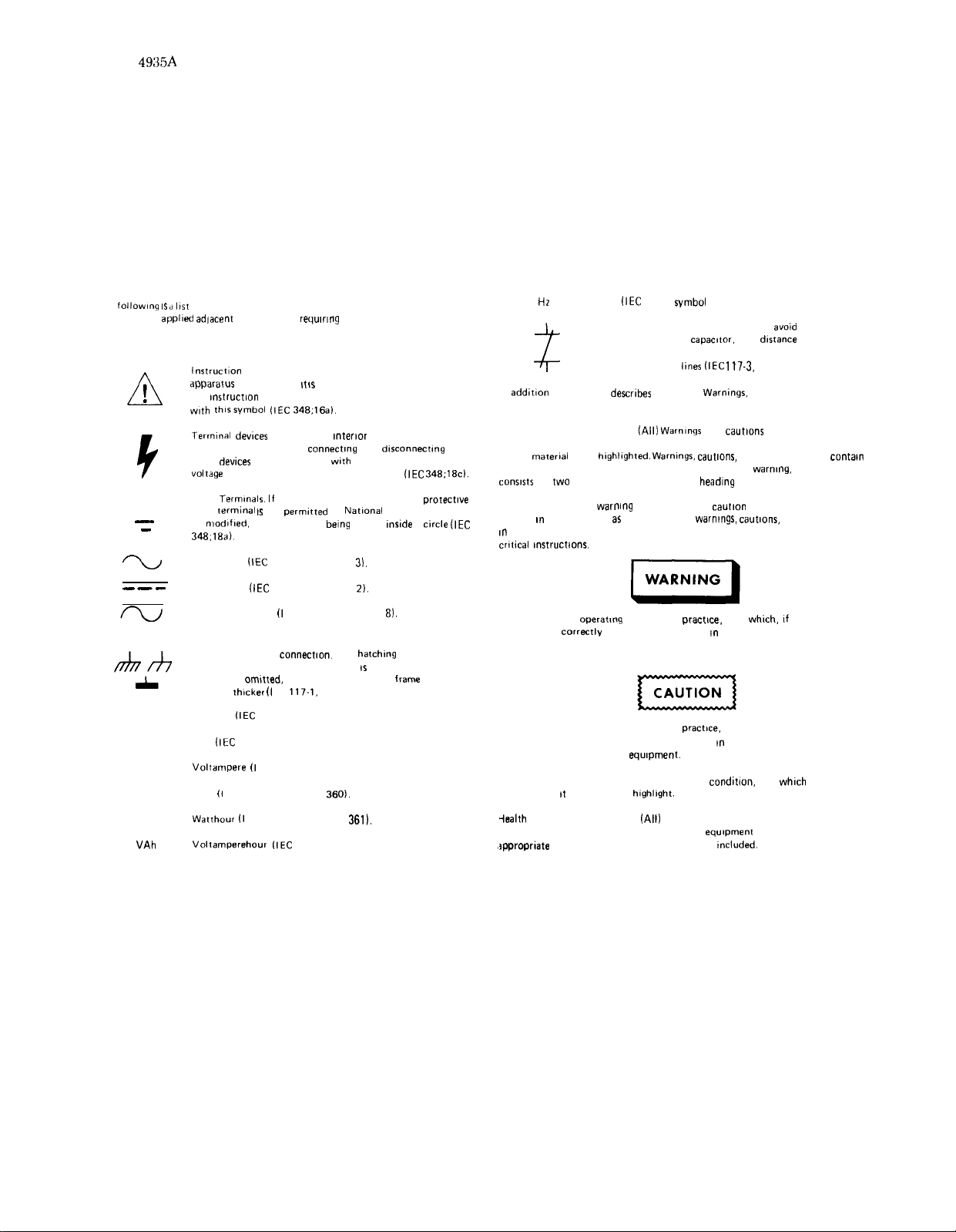
IEC Symbols
IEC SYMBOLS
The
follownq IS rl 1151
are normally
be placed on removable parts likely to be detached or lost.
A
1
-
-
---
VA
w
applwd adlacent
!
A
V
of key I EC symbols used by Hewlett-Packard. All symbols
to the device
lnstrucf~on
apparatus
the
wth thlssymbol (IEC 348;16a).
Termnal dewces
may be dangerous when
those
volrdge
Earth
earth
be
348.18a).
AC current
DC current
AC or DC current (I EC 1 17-l. symbol No.
pletely or partly omitted if there II no ambiguity. If the
hatching is
shall be
Ampere
Volt
Voltampere (I
Watt (I EC 1174, symbol No.
Manual symbol: If necessary. to preserve the
from damage !t IS necessary for the user to refer to
mstruct~on
dewces
shall be marked
exceeds 1 KV: The flash shall be red
Termunals. If
termmal 1s
modlfled.
for example, by
(IEC
fIEC
Frame or chaws
omated,
thrcker (I
(IEC
lltC
1174. symbol No. 357).
requur~ng
the symbol. They shall not
manual, then shall the apparatus be marked
fad from the
the use of this symbol for the
not
permttted
117-l. symbol No.
117-l. symbol No.
connection.
the line representing the
EC
1174, symbol No. 356).
EC 1174, symbol No. 358).
connecting
117.1,
symbol No. 87).
~ntertor
wth
by
bang
The
3601.
National
by live voltages that
to or
dlsconnectlng
the flash shown when the
Standards, it may
placed
irwde
3).
2).
8).
hatchmg
may be com-
frame
from
(IEC 348;lEc).
protectwe
a
circle (IEC
or chassis
HZ
z
In
addltlon
in HP Automatic Test System Manuals.
Warnings, cautions and notes.
to which each apples but notes may precede or follow applicable text depending
on the
material
procedural steps nor shall they be numbered. When a
consists
of
shall not be repeated above each paragraph. If it is ever necessary to precede a
paragraph by both a
appear m the sequence as noted, namely.
I”
the text shall be short and concise and be used to emphasize important and
critical mstructtons.
Hertz
(IEC
1174.
symbol
No. 365).
Contactor, normally closed. In order to
the symbol for a
horizontal (as drawn here) lines should be at least equal to
the length of those
the following
two
An
correctly
loss of life.
An operating procedure,
strictly observed, could result tn damage to, or
destruction of,
NOTE: An operating procedure,
it
describes
(All) Warmngs
to be
highllghted. Warnings, cautions,
or more paragraphs, the
warmng
and a note, or a
operating
procedure,
followed, could result
eqwpment.
is essential to
hIghlIght.
lines (IEC 117-3,
the use of
practtce.
practw,
capacitor.
the
deance
symbol No. 215.21.
Warmngs.
Cautions and Notes used
and
caut!ons
shall precede the text
and notes shall not
heading
warnings. cautions,
warmng,
WARNING, CAUTION, NOTE,
caution
and a note, etc. they shall
etc.
which. If
III
personal injury or
etc. which, if not
condmon,
etc.
avold
confusion with
between the
contan
caution, or note
notes. Such inserts
not
whwzh
Wh
VAh
Watthour (I
Voltamperehour (IEC
EC 1174, symbol No.
361).
1174, symbol No. 362).
-health
hazards precaution data.
factors, in the environment or use of the
,tppropriate
precautionary requirements shall be
(All)
When hazardous chemicals or adverse health
equipment
cannot be eliminated,
mcluded.
iii/(iv blank)
Page 5

Page 6
Model 4935A Table of Contents
TABLE OF
Section Title
I. GENERAL INFORMATION
l-l. Introduction.. ................................................... l-l
l-3. General
l-5. Instrument Identification..
l-7. Specifications.. .................................................
l-9.
Safety
Related Manuals............................................. l-4
1-12.
1-14. User Repair.. ...................................................
1-16.
Options
1-19.
Warranty.. ......................................................
1-21.
Recommended Test Equipment.. .................
l-23. Battery Operation
l-26. Charging the Batteries.. ...........................
l-29. Operating Temperature.. .........................
II. INSTALLATION
2-l. Introduction.. ..................................................
2-3. Initial Inspection.. ..........................................
2-6. Preparation for Use.......................................
2-7. Power Requirements.. ...................................
2-9. Line Voltage Selection..
2-11. Power Cable.. .................................................
2-13. Operating Environment.. ..............................
2-16. Storage
2-17.
Instrument Packaging ................................... .2-2
2-19.
III. OPERATION
3-l. Introduction....................................................
3-3. Self Check.......................................................
3-5. Error
3-7. Operating
3-9. Measurements
3-10. Measurement Principles ............................... .3-17
3-12. Input-Output
3-19. Level and Frequency Measurements..
1000
3-21.
3-24. Frequency Shift
3-26. Attenuation Distortion.. ................................
3-30. SF Skip ............................................................
Message Circuit Noise Measurements..
3-32.
3.40. Noise Measurements.....................................
3-42. Noise-with-Tone (Notched Noise)
3-45. Signal-to
Description.. ..................................... l-l
.............................
Considerations..
and Accessories..
..................................
.............................. l-4
(0pt.s 001 &
003) ..........
................................. 2-l
and
Shipment.. .................................
Environment..
Messages..
........................................... .2-2
............................................
Instructions
..................................
................................................
Switching ................................ .3-17
Hz Loss.. ................................................
.............................................. .3-18
...............3-22
Noise Measurement.. .................... .3-22
........
....
C:ONTENTS
Page Section Title
3-48. Signal Frequency Interference .................... .3-24
3-52. Impulse Noise.. .............................................. .3-24
3-55. Noise-to-Ground Measurement..
l-1
l-l
.1-4
l-4
..l-
4
l-4
l-6
l-6
l-6
.2-l
.2-l
.2-l
.2-l
.2-2
.2-2
.2-2
.3-l
.3-l
.3-l
.3-6
.3-7
.3-18
.3-18
.3-18
.3-19
..3-19
.3-22
3-59. Peak-to-Average Ratio
IV. PERFORMANCE TESTS
4-l. Introduction ...................................................
4-3. Equipment Required.. ..................................
4-5. Test
Record
...................................................
4-7. Self Check ......................................................
4-9. Performance Verification.. ...........................
4-12. Performance Tests........................................
4-13. Transmitter Flatness at +
4-14. Transmitter
4-15. Receiver Accuracy at t
& -4OdBm..
4-16. Autorange Test........................................
4-17. Filter Tests..
4-18.
Impulse Noise DAC Test.. .....................
4-19. Count Limit Test.. ...................................
4-20.
Termination Impedance
4-21. Hold Tone Dropout Detector
4-22.
4-23. Distortion
4-24. P/AR
Hold Circuit Test
Test
Test..
4-25. Noise-to-Ground(Std. dc Opt. 001).
V. ADJUSTMENTS/CALIBRATIONS
5-l. Introduction ...................................................
5-3.
Safety
Considerations.. .................................
5-5. Equipment
5-6. Instrument
5-9. Adjustment
Required.. ..................................
Access..
Locations...................................
5-11. Adjustments.. .................................................
5-13. t
5V,
+
Supply
14V,
and
Adjustments
5-14. Output Level & Transmit
Monitor
Loop Adjustments.. .................
5-15. Receiver Adjustments...................................
5-17. Notch Filter Adjustments.............................
5-18. Al3 P/AR Filter and Latch
Adjustments(0pt.s
5-19. Hold Circuit Adjustments.. ....................
Measurement.........3-2
Flatness at
..............................................
.............................................
....................................
........................................
..............................................
.................................
-14V
Power
......................................
001&003). ...................
................ .3-25
10dBm..
-40dBm..
1ldBm
Test..
Test........4-19
........
..........
..............
......
Page
5
.4-l
.4-l
.4-l
.4-l
.4-l
.4-2
.4-2
.4-4
.4-8
.4-10
.4-11
.4-14
.4-16
.4-17
.4-20
.4-21
.4-25
.4-26
.5-l
.5-l
.5-l
.5-l
.5-l
.5-2
.5-3
.5-4
.5-5
.5-7
.5-8
.5-9
V
Page 7
Table of Contents Model
4935A
TABLE OF CONTENTS
Section
VI. REPLACEABLE PARTS
6-l. Introduction..
6-3. Replaceable Parts List.. ...............................
6-5. Ordering Information ...................................
VII. MANUAL CHANGES
7-1. Introduction ....................................................
7-3. Manual Changes.. ..........................................
7-6. Manual Change Instructions.......................... 7-l
VIII. SERVICE
8-l. General Information ....................................
8-8. How Measurements are Made
8-10. Level
8-13. Noise.. ......................................................... 8-4
8-16. Noise-with-Tone ......................................
8-19. Signal-to-Noise.. .......................................
8-22. Impulse Noise ..........................................
8-26. Noise-to-Ground (Std & Opt. 001).
8-29. Peak-to-Average Ratio: P/AR
(0pt.s
8-32. Frequency Measurement.. ............................
8-34. Level
Measurement..
8-38. How to Compute Frequency and Level
Measurement .................................................
8-39. Level Calculation Example.. ...................
8-42. Control Theory of Operation.......................
8-44. MicroprocessortoInstrument.. ................... .8-11
8-45.
System
8-48. InstrumenttoMicroprocessor.. ................... .8-12
8-51. Operator to Microprocessor ........................ .8-12
8-52.
8-54.
Keyboard Interrupt.. ................................ .8-12
Receiver Impedance
8-57. MicroprocessortoOperator.. ......................
8-58. Displays..................................................... .8-13
8-60.
InstrumenttoOperator ................................ .8-13
8-62. Monitor Amp ........................................... .8-13
8-64. Beep Generator ....................................... .8-13
8-66. OperatortoInstrument ................................ .8-13
8-68. Miscellaneous Circuitry................................ .8-13
8-73. Receiver Theory of Operation..................... .8-15
8-76.
I/O
Termination ..............................................
Title Page Section Title
..................................................
....................
and
Frequency.. .............................
......
002&003) ....................................
.....................................
Latches.........................................
Switches..
.............. .8-12
Switching/Hold Circuits/
.6-l
..6- 1
.6-l
.7-l
.7-l
..8- 1
.8-3
.8-4
.8-4
.8-5
.8-5
.8-6
.a-6
.8-6
.8-7
.8-8
.8-8
.8-11
.8-H
.8-13
.a-16
(cord)
Page
8-80. Input Select/Notch Filter/
25dBAmp.. ............................................. .8-17
8-85.
8-97. Level Detectors ....................................... .8-19
8-100.
8-102.
8-104.
811.3.
8-126. Power Supply Theory....................................
8-128. AC Line Supplies ....................................
8-131. Regulators.. ..............................................
8-139. Charger Board Theory of Operation..
8-141. Battery Charging.. ...................................
8-144. Power Source Selection.. ........................
8-146. Relay Drive Circuitry.. ............................
8-148. Inhibit Circuit ........................................... 8-26
8-153. Maintenance ..................................................
8-1.55.
8- 157.
8-159. Component Replacement ......................
8-164. Soldering ..................................................
8-166
8-168. Disassembly .................................................... 8-29
8-169.
8-171.
8-173. Switchboard/Front Panel Removal..
8-175. Transmitter Board Removal.. ...................... .8-30
8-177. Reassembly.. ..................................................
8-179. Power Supply Troubleshooting.. .................
8-181. Minimum Core Troubleshooting................
8-183. Procedure .................................................. 8-35
8-186. Display Troubleshooting.. ......................
8-189. Control Troubleshooting..............................
8-190.
8-192. Control and Counting Section
8-194. Transmitter Troubleshooting ......................
8-196.
8-200.
8-202.
8-204. Filter and Signal Select Circuitry..
8-207.
8-210.
8-212. Receiver Troubleshooting............................
Noise Filter Circuitry.. ............................ .8-17
Impulse Noise Detectors.. ...................... .8-19
Transmitter .................................................... .8-19
Test Signal
Generation Method..
..........
.8-20
Circuit Description.. ................................ .8-21
.8-23
.8-23
.8-24
........
.8-25
.8-26
.8-26
.8-26
.8-28
Periodic Maintenance.. ........................... .8-28
Failure Maintenance.. .............................
.8-28
.8-28
.8-28
.
Cleaning.. ..................................................
Remove Case.. .........................................
.8-28
.8-29
Receiver Board/Shield Plate/
Battery Charger Board Disassembly..
........
..........
.8-29
.8-30
.8-31
.8-33
.8-34
.8-36
.8-36
Troubleshoot
Interrupt Circuitry.. .................................
Keyscan/
.8-36
Troubleshooting.. .......................................... .8-36
.8-37
Transmit Clock Generator.. ...................
.8-37
Transmitter Signature Analysis
Procedure.. ...............................................
Digital-to-Analog Conversion ...............
Output Amplifier.. ...................................
Transmit Monitor.. ..................................
........
.8-37
.8-39
.8-40
.8-42
.8-43
.8-43
vi
Page 8
Model 4935A
Table of Contents
TABLE OF CONTENTS
Section Title Page Section Title Page
8-217.
8-219.
8-222.
8-225.
8-227.
8-229.
8-232.
8-233.
8-235.
8-237.
8-239.
8-242.
8-246. Noise Filters ...................................................
8-248. Autorange ................................................. .8-49
8-250. Detector Troubleshooting.. ....................
8-252. Impulse Noise Circuitry.. ..............................
82.54.
8-255. Procedure .................................................
8-257.
Setup..........................................................
Overall Transmit Monitor
Transmit Monitor Signal ........................
Noise Filter.. .............................................
Simplified Autorange Check.. ................
Detector Select.........................................
Inputs from Front Panel/
Notch Filter/ 25dB Amp/Tone
Dropout Signal Path.. ..............................
Setup..........................................................
Input Transformer.. .................................
Noise-to-Ground Input Path
(Noise-to-Ground Units
Tone Dropout
Notch Filter ..............................................
Charger Board Troubleshooting .................
Charge Circuitry/Charge
Inhibit Circuitry .......................................
Signal
Test
.............
only)
............... .8-48
Path...................... .8-49
.8-44
.8-44
.8-45
.8-45
.8-46
.8-47
.8-47
.8-48
.8-48
.8-49
.8-49
.8-50
.8-50
.8-52
.8-52
.8-52
8-259. Relay Drive Circuitry,
Low Voltage Inhibit Circuitry.. .............
8-261.
8-263. Delay and Relay Drive Circuitry..
8-265. AC and Low Voltage Inhibit
8-267. Service Aids ...................................................
8-268. Service Selection of Input/
8-270.
8-272. Service Selection of Noise Filters
8-274. Procedure .................................................
8-276. Service Selection of Autorange
8-278. Procedure ................................................. .8-58
8-279. Hand Selection of
8-282. Hand Selection of C57 and
8-283.
Inhibit Circuitry AC and
Low Voltage.. ...........................................
Troubleshooting ......................................
Notch
Filter/25dB
Procedure.. ...............................................
by
Hand.. ........................................................
Gain for Service.............................................
(A3C57
for Desired Frequency
FiIters:
and
Response of Each Stage.. ................
Amp.. .............................
AX57
and
A3C160
for P/AR Units)
Response..
A3C160
..............
Cl60..
.........
........
.8-53
.8-54
.8-54
.8-55
.8-57
.8-57
.8-57
.8-58
.8-58
.8-58
.8-59
.8-60
.8-60
vii
Page 9
Table of
Contents
Model 4935A
LIST OF ILLUSTRATIONS
Section
l-l.
Model
4935A Transmission Impairment
Measuring
Title Page Section
................................................
Set
.1-O
l-2. Charge Acceptance at Various
Tempcraturcs..
2-l.
Lint
Voltage Selection.. ................................
3-l. Front and
Connectors/indicators..
3-2.
Measurements
3-3. Input-Output Switching
3-4. Level and Frequency Mcasurcments.. ........
3-5. Message Circuit Noise
3-6. C-Mcssagc Weighting Characteristic.. ........
3-7. 3
kHz
Flat Weighting Characteristic..
................................................ l-6
Rear
Panel Controls/
................................ .3-2
................................................
................................. 3-17
Measurements
......
.........
.2-l
.3-6
.3-18
..3-19
.3-20
.3-20
3-8. Program Weighted liltcr.. ............................. .3-21
3-9.
15
kHz
3-10.
Flat Filter ..........................................
SOkBit Filter.
................................................... .3-22
.3-21
3-11. C-Message Weighting with Notch
Characteristic.. ............................................... .3-23
3-12. Signal-to-Noise Measurement ..................... .3-23
3-13. Impulse Noise Waveform
Rcprcscntation..
3-14. Noise-to-Ground
Circuit Noise
............................................. .3-24
Related
to
Message
..................................................
.3-2.5
3-15. P/AR Transmit Signal Frcqucncy
Spectrum.. ....................................................... .3-26
3-16. P/AR Transmit Signal
Envelope..
...............
.3-26
4-l. Transmitter Flatness Test
at + 10
4-2.
Transmitter
at
-40 dBm
4-3. Reccivcr Test at + 11
and
-40
4-4. Autorangc
4-5. Filter
4-6. Impulse Noise
4-7. Count Limit
4-8.
Termination
4-9. Hold
4-10. Hold
4-11. Distortion
4-12. -40
dBm
4-13. Filter Circuits .................................................
4-14. P/AR Test.. ....................................................
.................................................... .4-2
dBm
Flatness Test
...................................................... .4-4
dBm
dBm
................................................... .4-8
Test
.............................................. .4-10
Tests..
....................................................
DAC
Test
............................. .4-14
Test
...........................................
Impedance Test.. ..................... .4-17
Tone
(Xrcuit
Dropout
‘Test..
Test
Detector Test..
......................................... .4-20
................................................
...........
Distortion Test.. ............................. .4-22
.4-11
.4-16
.4-19
.4-23
.4-25
4-15. Noise-to-Ground Test.. ................................. .4-26
4-21
Title Page
5-1. Output Level and Transmit Monitor
Loop Adjustments..
5-2. Receiver
Adjustments...................................
5-3. Hold Circuit Adjustments..
6-l. Exploded View Case and Covers..
6-2. Exploded
View
6-3. Exploded View Battery Option..
.......................................
..........................
...............6-4
Assemblies and Cables..
.................
7-l. A2 Switch Board Component Locator..
..
....
.5-4
.5-5
.5-9
..6- 5
.6-7
..7-10
7-2. A5 Charger Board Component Locator.....7-14
7-3. Partial A5 Charger Board Schematic..
.......
.7-14
7-4. Al4 Transmitter Board Component
Locator ........................................................... .7-15
7-5. Partial A4 and Al4 Schematic ...................... 7-16
7-6. Al4 P/AR Transmitter Board
Component Locator.. ....................................
7-7. A4 Transmitter Board
Locator
........................................................... .7-17
Component
7-8. Partial Power Supply Schematic.. ................
.7-16
.7-18
7-9. Al3 P/AR Receiver Board Component
Locator ........................................................... .7-19
7-10. A3 Receiver Board Component
Locator ........................................................... .7-20
7-11.
A3 Receiver Board Schematic
1
(Sheet
of 2) ................................................. .7-21
7-12. A3 Receiver Board Schematic
(Sheet 2 of 2) ................................................. .7-23
7-13. Al3 P/AR Receiver Board Component
Locator
........................................................... .7-25
7-14. A3 Receiver Board Component
Locator
........................................................... .7-26
7-15. A3 Receiver Board Schematic
Diagram (Partial). .........................................
.7-27
7-16. A4 Transmitter Board Component
Locator ........................................................... .7-28
7-17. Al4 Transmitter Board Component
Locator
...........................................................
.7-28
7-18. A4 Transmitter Board Schematic
Diagram
......................................................... .7-29
7-19. Al4 Transmitter Board Schematic
Diagram (Partial). ......................................... .7-30
7-20. Al4 Transmitter Board Schematic
Diagram (Partial). ......................................... .7-30
.......
........
.7-32
.7-33
7-21. A2 Switchboard Component Locator..
7-22. A2 Switchboard Schematic Diagram..
7-23. A3 Receiver Board
Component
VW
. . .
Page 10
Model 4935A
Table of Contents
LIST OF ILLUSTRATIONS
Section Title Page Section
Locator.. .......................................................... .7-34
7-24. Al3 Receiver Board Component
Locator.. ..........................................................
7-25. Receiver Board Schematic
Diagram (Sheet1of 2) ................................. .7-36
7-26. Receiver Board Schematic
Diagram (Sheet 2 of 2) ................................. .7-37
7-27. A4 Transmitter Board Component
Locator.. .......................................................... .7-38
.7-35
8-19. P/AR Signal Frequency Spectrum ..............8-41
8-20. P/AR Transmit Signal Envelope................
8-21. 20 Hz Waveform ...........................................
8-22. Transmit Monitor Test Output ...................
8-23. 4935A Signal
8-24. Al Front Panel Schematic Diagram............8-69
8-25. A2 Switchboard Component Locator..
8-26. A2 Switchboard Schematic Diagram..
8-27. A3 Receiver Board Component
7-28. Al4 Transmitter Board Component
Locator
............................................................ .7-39
8-28. Al3 Receiver Board Component
7-29. A4 Transmitter Board Schematic
Diagram (Sheet 1 of 2) ................................. .7-40
8-29. A3 Receiver Board Schematic
7-30. A4 Transmitter Board Schematic
Diagram (Sheet 2 of 2)
7-31. A5 Charger Board Component
7-32. A5 Charger Board Schematic
.................................
Locator......7-4
Diagram.......7-4
8-l. 4935A Main Block Diagram.. .......................
.7-41
2
3
.8-l
8-30. A3 Receiver Board Schematic
8-31. A3 Receiver Board Schematic
8-32. A3 Receiver Board Schematic
8-2. Voltage-to-Frequency Conversion
Characteristics ................................................. 8-7
8-33. A4 Transmitter Board Component
8-3. Voltage-to-Frequency Conversion
output .............................................................
.8-8
8-34. Al4 Transmitter Board Component
8-4. Frequency and Level Measurement
Timing.. ...........................................................
.8-9
8-35. A4 Transmitter Board Schematic
8-5. Control Circuitry Block Diagram................ .8-11
8-6. Receiver Block Diagram.. .............................
8-7. Switchboard Block Diagram ........................
8-8. Input-Output Switching ................................
.8-14
.8-15
.8-16
8-36. A4 Transmitter Board Schematic
8-37. A4 Transmitter Board Schematic
8-9. Filter Block Diagram .................................... .8-17
8-10. Autorange Block Diagram ........................... .8-18
8-38. A4 Transmitter Board Schematic
8-11. Stair-Step Sinewave.. ..................................... .8-20
8-12. Transmitter Block Diagram ......................... .8-21
8-13. Power Supply Block Diagram.. ....................
.8-23
8-14. Charger Board Block Diagram.. .................. .8-25
8-17. Instrument Troubleshooting ........................
8-18. Stair-Step Sinewave.. .....................................
.8-32
.8-39
8-39. A4 Transmitter Board Schematic
8-40.
8-41. A5 Charger Board Schematic Diagram......8-9 1
Title Page
.8-42
.8-43
.8-44
Flow
Block Diagram.. ...........
Locator ...........................................................
Locator ...........................................................
Diagram (Sheet1of 4). ................................
Diagram (Sheet 2 of 4).................................
Diagram (Sheet3of 4).................................
Diagram (Sheet 4 of4). ................................
.......
........
.8-67
.8-70
.8-71
.8-72
.8-72
.8-73
.8-75
.8-77
.8-79
Locator ........................................................... .8-80
Locator ........................................................... .8-80
Diagram (Sheet1of 5)................................. .8-81
Diagram (Sheet2of 5). ................................
Diagram (Sheet3of 5).................................
Diagram (Sheet 4 of 5). ................................
Diagram (Sheet5of 5). ................................
.8-83
.8-85
.8-87
.8-89
A5 Charger Board Component Locator....,890
ix
Page 11
Table of Contents
LIST OF TABLES
Model
4935A
Table
l-l.
l-2.
l-3.
2-l.
4-1.
4-2.
4-3.
4-4.
4-5.
4-6.
4-7.
4-8.
4-9.
4-10.
4-11.
4-12.
4-13.
4-14.
4-15.
4-16.
6-l.
6-2.
6-3.
Title Page Table
Specificalions..
Recommended
................................................. l-2
Test
Equipment.. ................. l-5
List of Parts Used for Performance
Tests
................................................................. l-5
HP Plug
Transmitter Flatness
Transmitter Flatnessat-40 dBm..
Styles..
............................................... 2-3
at +
10
dBm
............... .4-3
...............
.4-5
Abbreviated Transmitter Flatness................4-7
Receiver
Accuracy Test
Table ..................... .4-9
Abbreviated Receiver Accuracy
Test
Table.. ..................................................... .4-9
Autorange
..............................................
Test
.4-10
C-Message Filter Test................................... .4-11
3
kHz
Filter Test............................................ .4-12
15
khz flat Filter Test.. .................................. .4-12
Program Filter Test....................................... .4-12
50
kBit
Filter Test.. ........................................ .4-13
Test..
Notch Filter
Impulse Noise
Filter Circuit
.......................................... .4-13
DAC Test ............................. .4-15
Parts List.. ............................... .4-23
Abbreviated Distortion Test ........................ .4-24
P/AR Filter
Responses
................................ .4-25
Reference Designation and
Abbreviations
Manufacturer
Replaceable
................................................. .6-2
Code List
...............................
Parts.. ........................................
.6-8
.6-9
Title Page
7-l. Manual Changes.. ..........................................
8-l. Measurements
8-2. Noise Amplification..
Summary.. ............................
.....................................
.7-l
.8-3
8-5
8-3. Reference Signatures.. .................................. .8-38
8-4.
Wideband
8-5. 5
kHz
8-6. Output Select MUX.. ....................................
8-7. Transmit Monitor Test.................................
8-8.
A3UlB
8-9. TP3 Voltages
S-10.
Hand Selection of Noise Filters ..................
8-11. Autorange
8-12. Hand Selection of C57 and
8-13. 4935A C-Message
8-14. 4935A 3
8-15. 4935A
Filter Response ...........................
Low Pass Filter Response
.................8-40
Voltages ...........................................
................................................. .8-51
States........................................... .8-59
Cl60..
..............
Filter..
.............................
kHz
Filter.. ...................................... .8-61
kHz
Filter...................................... .8-61
15
S-40
.8-41
.8-43
.8-51
.8-58
.8-60
.8-61
8-16. 4935A Program Filter.. ................................. .8-61
8-17. 4935A 50
8-18. 4935A
kBit
Filter.. .................................... .8-62
Notch
Filter.. ...................................... .8-62
8-19. 4935A P/AR Filter ....................................... .8-62
8-20. 4935A 150
8-21. 4935A 110
8-22. Bell
8-23. Bell 410093kHz
8-24. Bell 4100915kHz
8-25. Bell 41009
8-26. Bell 41009
8-27. Bell 41009
8-28. Bell 41009 Notch
kHz
Low Pass Filter ..................
kHz
Low Pass Filter
C-Message Filter.. ......................
41009
Filter.................................
Filter.. .............................
Program Filter.. .......................... .8-64
50
kBit
Filter.. ............................. .8-65
P/AR Filter ................................
Filter.. ...............................
.8-62
.................. .8-63
.8-63
.8-64
.8-64
.8-65
.8-65
x
/(xi blank)
Page 12

Page 13
(hctral Inii,rmi,ti~,,,
Model 4935A
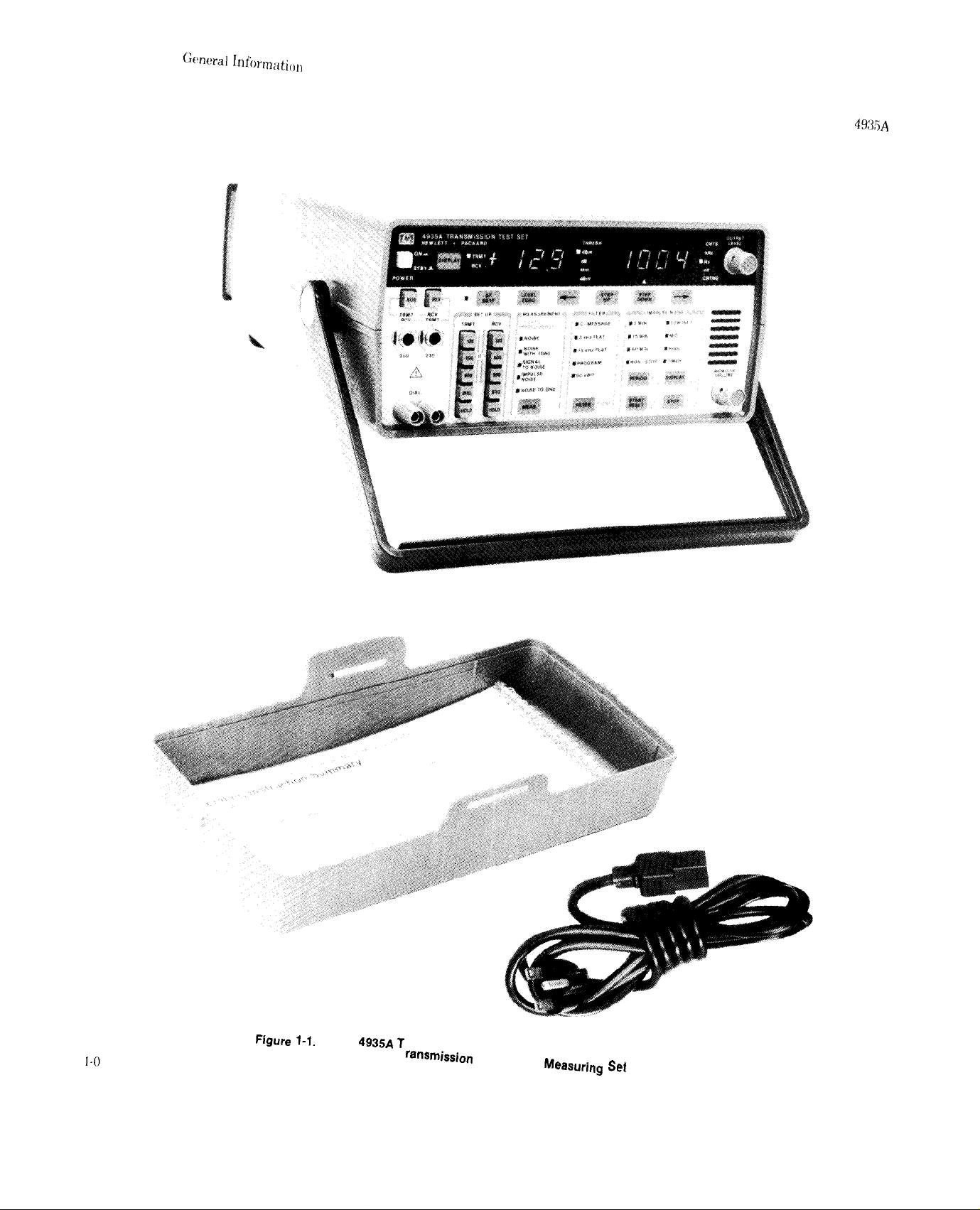
Figure f-1.
Model
4935A f
ransnhdon
Impairment
Measuring set
Page 14
Model 4935A. t
General Information
SECTION I
GENERAL INFORMATION
l-l.
1-2.
the HI’ Model
49XA
following information:
INTRODUCTION
This Operating and Service manual contains information to install, operate, maintain, and service
49:{5A
Transmission Impairment Measuring Set (TIMS). Figure 1-l shows the HP Model
with cover and power cord. The manual is divided into eight major sections which provide the
SECTION I. GENERAL INFORMATION. Provides identification, specifications, related
manuals, and user-repair information.
SECTION II. INSTALLATION. Contains unpacking and inspection information, power
requirements, packaging, and storage instructions.
SECTION III. OPERATION. Includes an explanation of controls, connectors, indicators, and an
automatic self check procedure. Describes measurement principles and front panel instructions for
making each measurement.
SFCTION
instrument’s performance is in accordance with the specifications.
SECTION V. ADJUSTMENTS. Provides adjustment and calibration procedures.
SECTION VI.
replaceable parts.
SEXTION
instruments with earlier serial numbers.
IV. PERFORMANCE TESTS. C’xtves
REPLACEARLE
VII. MANUAL CHANGES. C
PARTS. Lists and identifies the instrument assemblies and
or
ams
test procedures required to verify that the
information to backdate the manual fort
SECTION VIII. SERVICE. Includes theory of operation, troubleshooting procedures, flowcharts,
component locators, and schematic diagrams.
1-3.
l-4.
data and voice impairments. The frequency range over which measurements are made is 20 Hz to 110 kHz,
in steps of I, 10, 100, 1000, or 10,000 Hz. There are four permanently stored, fixed frequencies -404, 1004,
2804. and
1-5.
l-6. A IO character serial number (OOOOAOOOOO) is inscribed on the rear panel. The first four digits and
the letter are the serial prefix. The serial prefix will change only if changes are made to the instrument; a
Manual Change Sheet will be included with the manuals of any instruments affected.
form the serial suffix which is unique to each instrument.
1-7.
l-8. Instrument specifications are listed in Table I -1.
GENERAL DESCRIPTION
HI’ Model
271:s
49XA
is a Transmission Impairment Measuring Set (TIMS) which measures wideband
Hz. Any other four frequencies may be temporarily assigned and stored by the user.
INSTRUMENT IDENTIFICATION
Thelast
SPECIFICATIONS
five numbers
l-l
Page 15
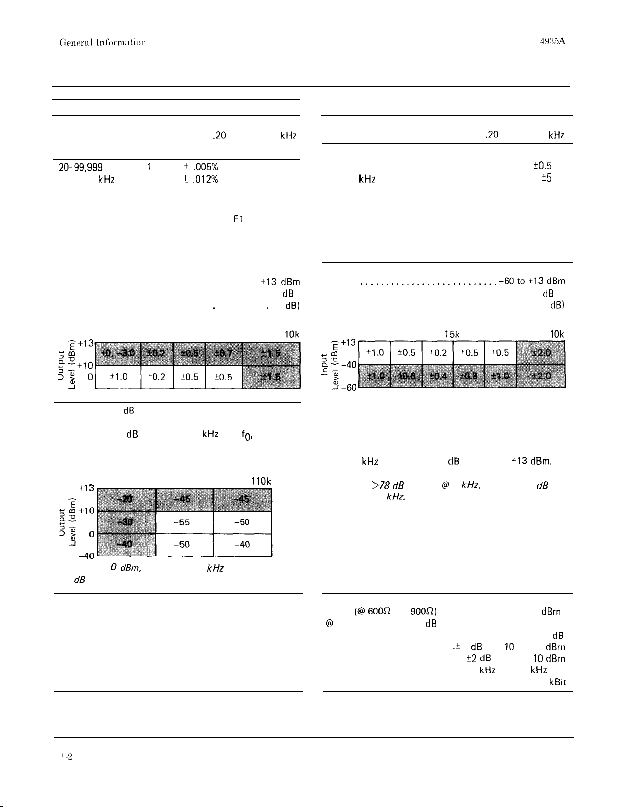
Table l-l. Specifications
Model
49:EA
TRANSMITTER
Frequency
Frequency Range . . . . . . . . .
Resolution Accuracy
1
20-99,999
100-l 10
Store and Recall Functions
SK Skip . . . At power up skips a band from 2450-2750 HZ
Frequencies . . . . . At power up Fl is 404 HZ
Level
Range . . . . . . . . . . . . . . . .-40 to
Resolution . . . . . . . . . . . . . . . . . . . . . 0.1
Flatness . . . . . . . . . . . . . . . . . _ . . . . . . . _ (in
z+13
+im
g;+1;
3
Hz
kHz
20 200
-40
Hz
10 Hz
FREQUENCY, Hz
15k
f .005%
t .012%
60k 85k
.20
Hz to 110
of output frequency 20-9.999 Hz 1 Hz
of output frequency 10-110
F2 is 1004 Hz
F3 is 2804 Hz
F4 is 2713 Hz
kHz
+13 dl3m
dB
dB)
1
IOk
RECEIVER
Frequency
Frequency Range.. . . . . . . . . . . .
Resolution Accuracy
kHz
Level
Range .
Resolution . . . . . . . . . . . . . . . . . . . . . . . . . . . . . . 0.1
Accuracy . . . . . . . . . . . . . . . . . . . . . . . . . . . . . (in
5:
Q---40
K.s
.._........................
20 50 200
z-+13
10 Hz
FREQUENCY (Hz)
15k
.20
60k
Hz to 110
kO.5
-6Oto+13dBm
85k
3-60
+5
dB
1
kHz
Hz
Hz
dl3)
IOk
Distortion: (in dB from fundamental)
(Includes harmonics, spurious and background noise within
a filter with a 3 dB bandwidth of 4
is greater.)
FREQUENCY (Hz)
_
30 Hz
At 1004 Hz, 0
65 dB down from the fundamental.
Message Circuit Noise
Transmitter is quiet terminated
100 Hz 4k
dBm,
THD using a 4
kHz
or 4
f0,
kHz
filter is more than
whichever
IlOk
Receiver accuracy not specified below 500 Hz when using
13562 termination.
At 1004
Cross talk:
octave above 4
Message Circuit Noise
Range (@
@
Resolution . . . . . . . . . . . . . . . . . . . . . . . . . . . . . . . . . 1
Accuracy . . . . . . . . . . . . .
Filters . . . . . . . . . . .
kHz
accuracy is fO.l dB from -20 to
>78 dB
6OOa
13516 lower limit is 7 dB higher
isolation @ 4
kHz.
and
9OOn)
. . . . . . . . . . .O to 100
. . .+ 1 dB from IO to 100
.C-Message, 3
+I3 dBm.
kHz,
decreasing 6 dB per
+2 dB
from 0 to IO
kHz
Flat, 15
Program, 50
kHz
dBrn
dBrn
dBrn
Flat,
kBit
dB
Specifications describe the instrument’s warranted performance. Supplemental characteristics shown in shaded areas or in
italics are intended to provide information useful in applying the instrument by giving typical, but non-warranted
performance parameters.
Page 16
Model
4935A
General Information
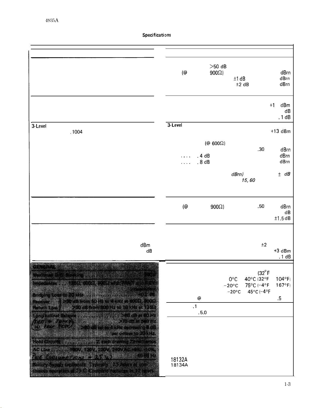
Table l-l.
TRANSMITTER
Noise with Tone
Frequency . . . . . . . . . . . . . . 1004 Hz fixed tone
(For other specifications, see Level and Frequency)
Signal-to-Noise Ratio
Frequency . . . . . . . . . . . . . . . . 1004 Hz fixed tone
(For other specifications, see Level and Frequency)
3-Level
Impulse Noise
Frequency . . . .
(For other specifications, see Level and Frequency)
Noise-to-Ground
Transmitter is quiet terminated
P/AR (Optional)
Frequency . . Signal spectrum is a complex pulse train of
Level Range . . . . . . . . . . . . . . . . . . . . .-40 to 0
Resolution . . . . . . . . . . . . . . . . . . . . . . . . . . . . 1
.1004
Hz fixed tone or quiet terminated
depending on filter selection
16 frequencies between 140 Hz and 3890 Hz.
SpecificatilJns
dBm
dB
(Continued)
RECEIVER
Noise with Tone
Notch Filter. .....
Range (@ 600R and
Accuracy .................?I dB from 20 to 100
(For other specifications, refer to Message Circuit Noise)
Signal-to-Noise Ratio
Signal Level Range
Ratio Range
Resolution .................................
3-Level
Impulse Noise
Level Range
Notch Filter. ................... .See Noise with Tone
Threshold Ranges (@
Low .............................
Mid
High : : : :....
Loss of Holding Tone Indication
Threshold Accuracy (above 40
Count Timer ............... 5,
Count Range ............... O-9999 for each threshold
Count Rate
Noise-to-Ground
Range (@ 600R and
Resolution
Accuracy
P/AR (Optional)
P/AR Range. .................. .O to 120 P/AR units
Resolution ........................... 1 P/AR unit
Accuracy (from 30 to 110 P/AR units) ...+2 P/AR units
Level Range
Resolution
.................................. 1
................................
>50 dB
900R)
..................
........................... IO to 45
....................... .-40 to
.4 dB
above Low to a maximum of 109
.8 dB
above Low to a maximum of 109
............................. 8per sec.
....................... .-40 to +3
................................
rejection from 995 to 1025 HZ
..............
*2 dB
from 10 to 20
.-40 to +I 3
6OOfi)
............ Minus sign
............
dBrnl
15,60
min. or non-stop
............
9OOfi)
IO-100
.30
to 109
.50
to 130
dBrn
dBrn
dBrn
dBm
.I dB
+I3 dBm
dBrn
dBrn
dBrn
+ 1
dBrn
+I .5 dl3
dBm
.I dB
1
dB
dB
dB
Temperature Range:
Operating . . . . . . . . . . . . . . 0°C to 50°C
with batteries
Storage . . . . . . . . . .
with batteries
Warm up time @ 20°C for stated accuracy . . . . . . . . .5 min.
Dimensions .I 1.2 x 25.9 x 28.6 cm (4.4 x 10.2 x 11.25 in.)
Weight . . . . .
OPTIONS
001
. . . . . . . . . . . . . . . . .
002 Adds P/AR measurement in place of Norse-to-Ground
003 . . . . . . . . . . . . .
ACCESSORIES:
15513A . . . . . . . . . Test cord w/31 0 male at both ends
18132A
18134A
18161 A
.5.0
kg (11 Ibs.), 6.5 kg (14 Ibs.) with battery
. . . . . . . . . . . . . . . . . . . 19” rack mount adapter
. . . . . . . . . . . . . . . . . . . . .
. . . . . . . . . . . . . . . . . . . . . , . . . . . . .
O°C
to
-20°C
to
-2O’C
to
Adds rechargeable battery pack
Adds both battery pack and P/AR
Deletes Noise-to-Ground
Soft pack carrying case
(32’F
40°C (32OF
75’C (-4OF
45’C (-4’F
Ladder bracket
to 122°F)
to
104OF)
to
167OF)
to 113°F)
I-3
Page 17
(;cnt~r:tl Inf’orm;rtIotl
1-9. SAFETY CONSIDERATIONS
1-12. RELATED MANUALS
1
1:;
( lI)t.ritting int’t~rtnation
is
summariztd
on it
t,arcl
in
the instrumt~nt t‘ovtsr.
l-14. USER REPAIR
I I
.-I.1 ntctrnal rthpairs tcl thta
c,ont;it.t thus tlta;lrtsst
t
It~u,l~~tt-~‘at,kartl Sales antI Servit,ta Of’fit~,
instrument should
1-16. OPTIONS AND ACCESSORIES
()I)( eon 002: Adds 1’ Al< (I’ta;ik! Avrragts Ratio) mr;lsurt~mrnt
t)rl dents by ;tuthoriztd rtbpair shops
listed at
the r(‘ar
in
of’ this manual.
Plato
of’
only.
I~orassistant~t~,
Nois+to-(;round
1 -4
I -%(I.
Itlstrumr~nt
warranty is as
listctl
on
thth insidtx of’ the f’ront c’ovt’r. Hattc~ry
1-21. RECOMMENDED TEST EQUIPMENT
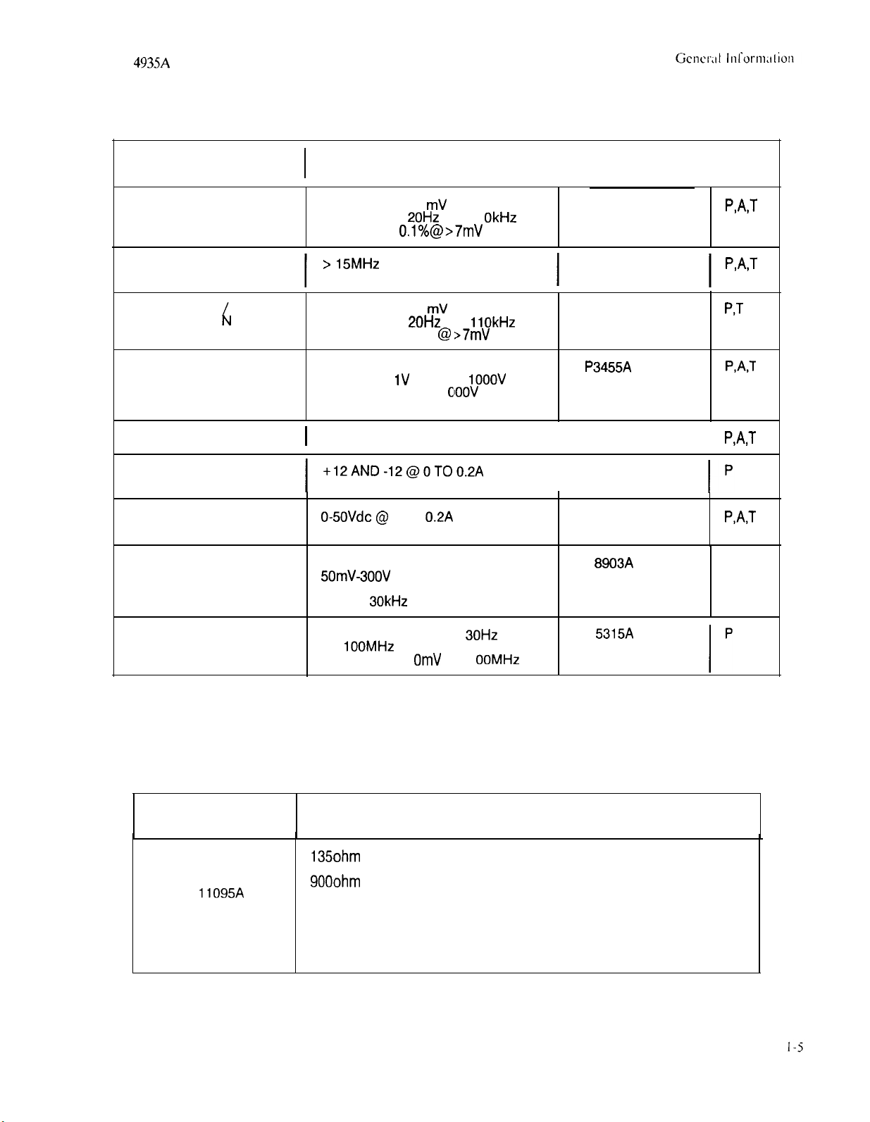
l-22.
m;,y tit) llS~‘(l
tit~t~~~rnmc~ntlt~tl ttsst tquipmt~nt
is
listed
in
‘I’whlt~
l-2. Equipment with
warranty is 90 days
quivnlcnt
characteristics
Page 18
Model
4935A
Table
INSTRUMENT
AC CALIBRATOR OUTPUT LEVEL 1 mV TO 1 OV
OSCILLOSCOPE
SYNTHESIZER OUTPUT LEVEL 1 mV TO 1 OV HP 3325A
FUNCTION GEIcERATOR FREQUENCY: 20Hz TO 110kHz
MULTIMETER AC AND DC FUNCTIONS
DIGITAL MULTIMETER
DUAL OUTPUT POWER
SUPPLY
I
1 DC CURRENT: 1 AMF’ MAX
1-2.
CRITICAL SPECIFICATIONS
FREQUENCY: 20Hz TO 11 OkHz
ACCURACY
>
15MHz BANDWIDTH
A VS B CAPABILITY
ACCURACY 0.1% @
AC VOLTS: 1V MIN. TO
DC VOLTS: .l V TO 1
BALANCED INPUT
+12AND-12@OTO0.2A
Recommended Test Equipment
O.l%@>7mV
>7mV
1OOOV
OOOV
MODEL
RECOMMENDEDIUSE*
FLUKE 5200A
OR EQUIVALENT
HP 1740A
H P3455A
HP 3466A
I
HP 6234A
I
PAT
PAT
P,T
PAT
PAT
DUAL RANGE
DC POWER SUPPLY
AUDIO ANALYZER
COUNTER RANGE: AC COUPLED 30Hz
*P = PERFORMANCE TESTS A = ADJUSTMENTS
Table 1-3. List of Parts Used for Performance Tests
PART NUMBER
(IF APPLICABLE)
0698-7364
0698-7408
0698-6344
HP
11095A
1250-0781
1251-3757
0493560014
OdOVdc @
INPUT VOLTAGE RANGE
50mV-300V
BANDWIDTH 500kHz
FILTER 3OkHz
TO
100MHz
SENSITIVITY: 1 OmV TO 1 OOMHz
135ohm 1% RESISTOR
6000hm 1% RESISTOR
900ohm
TERMINATION, 6000hm BNC-TO-BNC
BNC-TEE FEMALE
BNC TO TYPE 310 POMONA NO. 2798 OR EQUIVALENT
BNC TO DUAL BANANA JACK POMONA NO. 1296
DUAL BANANA COMPONENT CARRIER POMONA NO. 1
DIAGNOSTIC SERVICE KIT
0 TO
0.2A HP 6218A
DESCRIPTION
1% RESISTOR
HP 8903A
HP 5315A
T = TROUBLESHOOTING
PAT
P
330-ST
Page 19
General Information Model
497’,A
t
<
l-23.
l-24. Nickel-Cadmium batteries enable the 4935A to be used in areas removed from AC power.
Typical operating time
BATTERY OPERATION (Options 001 and 003)
is2.5
hrs when fully charged.
The batteries are trickle-charged whenever the
instrument is connected to an AC source and the POWER switch is in STBY.
1 -EL
Regular discharge-charge cycles are recommended to maintain battery capacity. The instrument
should be operated until batteries are discharged (instrument stops working) then recharged, at least every
30 days. Normal recharge time is about 17 hours. Typical battery life under normal operating conditions
should he at least 100 charge-discharge cycles.
l-26.
l-27.
Charging the Batteries
The internal battery pack consists of three rechargeable battery packs
(+6V, +156V,
and
-156V).
These provide typically 2.5 hours of continuous use without recharging. To recharge the battery packs, connect
the HP 4935A to an AC power source and press the power switch to STBY. Normal recharge time is about 17
hours.
I-28.
greater charge capacity if charged between
the
60-70’s
The batteries may be charged at temperatures between 5°C and
5’C
charge
acceptance
falls off’
and 25°C
as shown in Figure
1-2.
(41°F
For example, a cell charged at 45°C accepts about
and
4O’C
(41°F and
77’F).
At temperatures above 25°C
104”F),
but have
of its rated capacity. Temperatures below 5°C cause pressure to build up within the cell as it is
charged, which could result in venting of the cell. This results in a permanent degradation of the battery
capacity due to loss of electrolyte.
l-29. Operating Temperature
I-30.
between
Normal operating temperature of the I-IP 4935A with batteries (options
-2OOC
and
+40°C.
However, there will be a loss of capacity when operating at the extremes. At low
001
and 003) should be
temperatures, the batteries cannot fully discharge even if they were fully charged at room temperature. At high
temperatures this same effect take
place
to a lesser degree, in addition to the problem of charge acceptance
previously mentioned.
100% EFFICIENCY
8
U
CHARGE INPUT (% OF NOMINAL CAPACITY) -
0 2 4
CHARGING TIME IN HOURS
40 80 120 160 200
O.IC
CHARGE RATE
G
8
lo
12 14 16 18
- O.lC
CHARGE RATE
20
l-6
Figure 1-2. Charge
Acceptance at Various Temperatures
Page 20
SECTION II
INSTALLATION
Installation
2-l.
2-2.
antI storagcb
2-3.
2-4.
INTRODUCTION
This section contains information on initial inspection, preparation
and shipment. Table 2-l shows all power cords available.
for
use, power requirements
INITIAL INSPECTION
Inspect the shipping container for damage. I“ the container or cushioning material is damaged,
keep it. Check the contents of the shipment for completeness, then check the unit mechanically and
electrically. Refer to Section IV for electrical checks.
2-5.
officbe
If the unit is mechanically damaged or fails electrical tests, notify the carrier and the nearest HP
(listed at the rear of this manual). Hewlett-Packard will arrange for repair or replacement of the
instrument without waiting for claim settlement.
2-6.
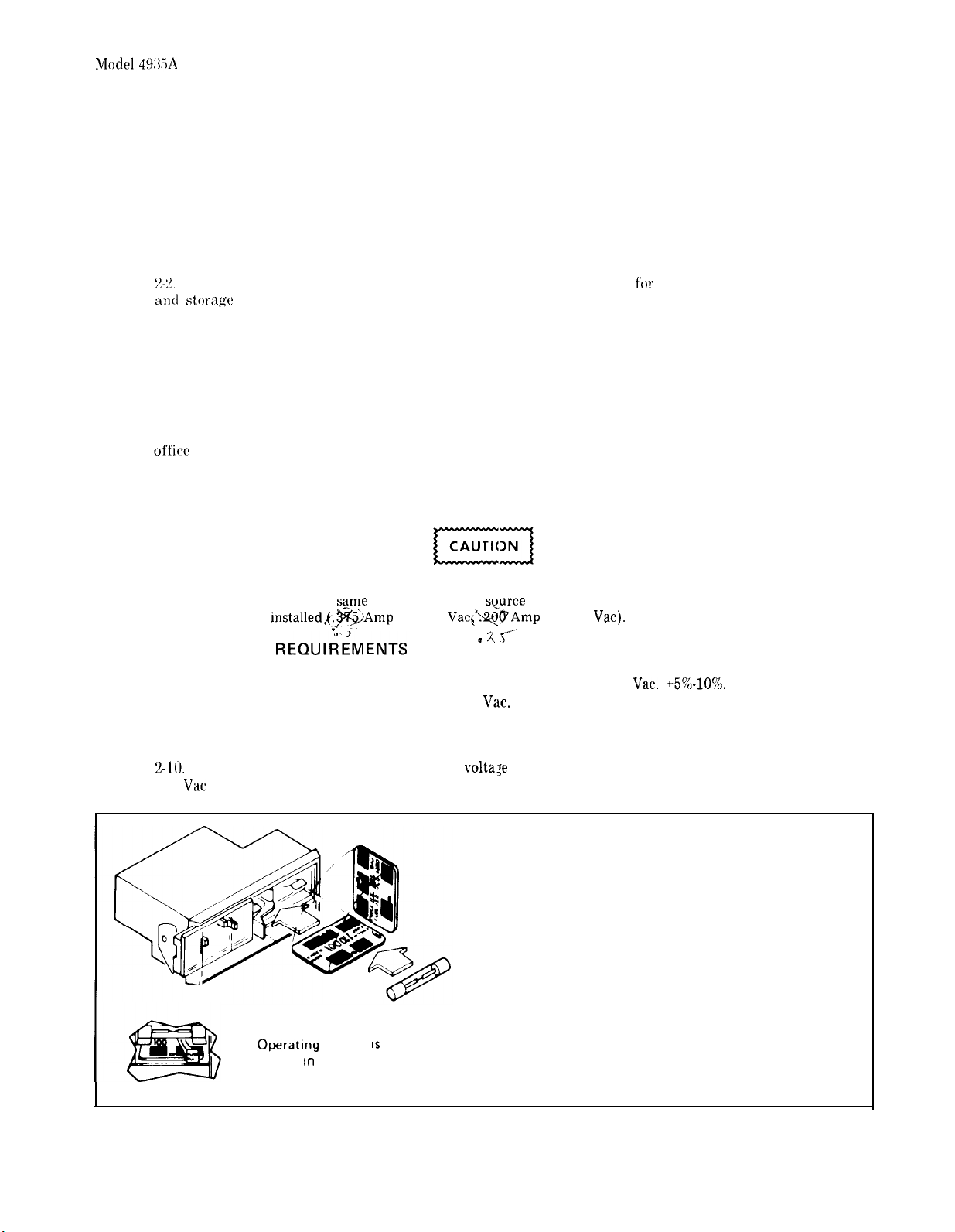
PREPARATION FOR USE
Before connecting this instrument to an AC power source, be sure that the rear panel line
module is set to the
2-7.
2-8.
voltage is
POWER
This instrument requires a power source of 100, 120, 220, or 240
installedk.BiAmp
REOlJlk’lENTS
single phase. Power consumption is no more than 25
szme
voltage as the AC
-
for 120
so_urce
Vac<&Q@Amp
(I A. SC
Vat.
and that the correct fuse for that AC
for 220
Vat).
Vat. +5’%-lo%,
48 to 66 Hz
2-9.
2-10.
120
LINE VOLTAGE SELECTION
Figure 2-1 provides instructions for line
Vat
operation.
voltasje
selection. Card and fuse are factory installed for
I
PROCEDURE
1. Slide cover door to left (the line power cord
must be disconnected).
2. Rotate FUSE PULL to left. Remove the fuse.
3. Remove the PC board by pulling it out. Select
operating voltage by positioning PC board to
show the desired voltage on top-left side,
4. Reinsert the PC board.
Operatang
shown In module window.
voltage
1s
5. Rotate FUSE-PULL back into normal position
and reinsert fuse. Use caution to select correct
fuse value.
I
Figure 2-1. Line Voltage Selection
2-1
Page 21
Installation
2-11. POWER CABLE
Any interruption of the protective (grounding) conductor (inside or outside the
instrument) or disconnecting the protective earth terminal can make this
instrumenl dangerous. Intentional interruption is prohibited.
Model
49:&A
2-12.
threewIre ac
This instrument is supplied with a three-wire power cable. When connected to an appropriate
power receptacle, the cable grounds the instrument chassis.
2-13. OPERATING ENVIRONMENT
2-14.
+122”F).
2-15.
R.H. @ 40°C. However, the instrument should be protected from temperature extremes which cause
condensat.ion
TEMPERATURE. The instrument may be operated in temperatures from 0” to 50°C (32°F to
Temperature for battery unit operation is 0” to
HUMIDITY. The instrument may be operated in environments with humidity from 5% to 95%
within the instrument.
40°C
(32°F to 103°F).
2-16. STORAGE AND SHIPMENT
2-17. ENVIRONMENT
2-18.
2-19.
2-20.
obtained through Hewlett-Packard sales and service offices listed at the rear of this manual. If the
instrument. is returned to HP for repair, attach a tag listing the type of service or repair needed. Include
return address, model number, option number (if applicable) and complete serial number. Also, mark the
container ”FRAGILE” to ensure careful handling. In any letters, refer to the instrument by model number,
option number (if applicable) and complete serial number.
The 49:15A
Temperature:
Humidity: 90% R.H. @ 65°C
(all options) may be stored and shipped within the following environmental limits:
-20°C to
(-4OF
to
t45”C
+113”F)
Do not store or ship where temperature extremes will
cause condensation within the instrument.
INSTRUMENT PACKAGING
ORIGINAL PACKAGING. Containers and packing material used in factory packaging can be
2-2
Z-2 I.
materials:
a.
b.
c.
d.
2-22.
please complete one of the blue tags located at the back of this manual and attach it to the instrument.
OTHER PACKAGING. Use these general instructions for packaging with commercially available
Wrap the instrument in heavy paper or plastic. If shipping to an HP Sales or Service Office, include
a tag listing type of service needed, return address, model number, option number (if applicable)
and complete serial number.
Use a strong shipping container such as a double-wall carton with 275 Ibs. burst test.
Use a layer of shock absorbing material, 70-100 mm (3-4 in.) thick. This provides a firm cushion
and prevents movement inside the container. Protect the front panel with cardboard or the front
cover.
Seal
the carton securely and mark it “FRAGILE” to ensure careful handling.
‘I’A(;GING
FOR SERVICE. If the instrument is being returned to Hewlett-Packard for service,
Page 22
Installation
Table 2-1. HP
Stralghr ‘NEMA5 15P
Straight ‘NEMA5 15P
Plus Stvles
Black
For Use
In Country
United
Kingdom.
Cyprus
Nlgerla
Australea
New Zealand
East and
Europe, Saudi
Arabta
So
Umted
Canada.
Japan
Wesl
Egypt.
Africa. lndla
unpolarlred in
many natIons
Stares
llOOV
or
c-
81202104 3
8120.0698 6
8120 1957 2
8120 2956 3 90’
8120 1860 6
,-
250V
250V
250V
-i
250V 8120-4600
8120.4211
Straight ‘SEVlOl
1959 24507
Type 12
Slralght ‘NEMAG 15P
Straight ‘DHCK 1117
Straight ‘CEE22 \/I
6yslerns Cablner use’
8 StralrJhl BS 5461SABS
7 90”
Taiwan
1
164
79
79
79
98
98
Gray
Gray
Gray
Black
Black
Swtrerland
United States
Canada
Denmark
‘Part number shown for plug IS
lncludlng
E Earth Ground. L
plug
Lone
N
Industry ldentlfler
Neutral
for
pluq
only
Num xr
shown for cable IS HP Part Number for complete cable
2-t3/(2-4
blank)
Page 23

Page 24
Operation
SECTION
III
OPERATION
3-1.
:3-z.
c-odes ( Err-c,otlrs).
self’ check prc,cedurrs
necessarv.
3-3.
:1-4.
major circuits are checked and any problems are identified. Self check does not
specifications.
instrument to pass any self check procedure indicate? a malfunction that can possibly affect other
mr:asurrmc~nt.s.
3-5. ERROR MESSAGES
3-6.
through thr filters.
0 through 6 indicate there are problems during self check. Errors 7 and 8 highlight problems during a
particbular
measurc~mc~nt.
FREI$UF:N(‘Y. &en
measuremrnts
indic,ativc
INTRODUCTION
This section contains information on front and re jr panel features, self check procedures, and error
Also covered are the principles of operation for all measurements. If any of the automatic
fail
acceptable
limits as specified in the checks, then adjustment or repair may be
SELF CHECK
The
self check procedures are performed automatically at power-up by the instrument. Most of the
verif.y
performance
I’rrformance
W
hthn
the
measurement. Other indications of errors during measurement are described by the particular
After startup self-check, the instrument automatically goes into Transmit Mode,
affected hy the displayed errors. Errors 0 t
of a system level failure more than a filter failure.
checks verify that the instrument meets published specifications. Failure of the
4!4:ki,A
is powered up, the instrument automatically transmits a signal into its receiver
The
signal is checked after each filter, to verify that it is within acceptable limits. Errors
if error messages occur, the instrument continues to operate correctly except for those
Trough 5
(Err O-Err 5) followed by Error 6 (Err 6) is
IXVEI,
I)15pla> otl F:rrors arc’:
F1rr
0
I*;rrl ~~
b.rr
2
~
I.:rrS
Krr
4
~~
Err
5
~~
Krr
6 Error in
l+Zrr
7
~
Krr
8
‘I’c~st signal cannot h(x measurt~d thrclugh C-Mt~ssagc~
‘I’c~sl
‘I&t
‘I’tast
Test
‘I’esl
Err 0.
Received
‘I’ONE
IMPULSE NOISE threshold is
rctc&e impedanchtr
signal
c,a~~trot h(a mclasurc,d
signal cannot
signal
signal
signal
cannot hc measurc>d thrclugh
cannot
c-annot
I,EVEI2 FREQIJENCY
1004
11~
or SIGNAL
RCVL2:
filter.
through 3
hc‘ mcxasurrd
he measured
be measured through P/AR filter. If not a P/AR unit refer to
tone is below -16
‘1’0
NOISE.
as follows:
13512
60012
90012 107 d Hrn
through 15
thrc.+$
signal path.
sct1
too high. Thr
kHz
flat
kHz
Program filter.
50
kHit
dBm
or above
116
dHrn lippclr
109 dBrn
filt~~r.
flat
filter.
upper
filtclr.
+13 dBm
Limit
in
NOISE:
limit varies with the
WITH
3-l
Page 25
Model
4935A
0
I
5
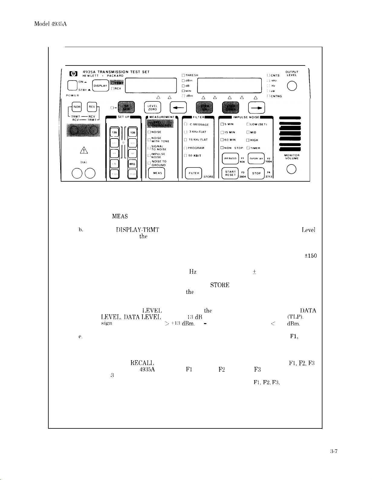
Figure 3-1. Front and Rear Panel Controls/Connectors/Indicators
Page 26
Model
49XiA
Operation
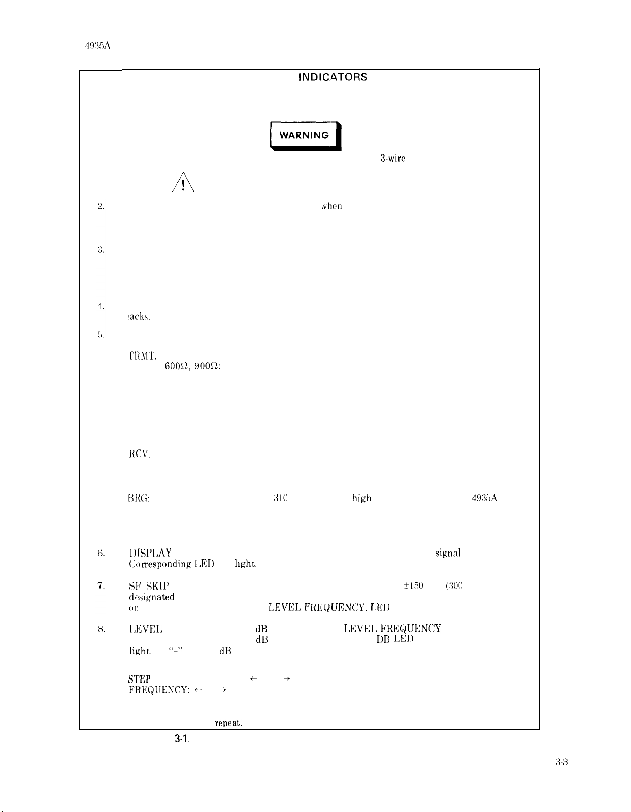
1.
CONTROLS, CONNECTORS AND
INDIC.ATORS
Power Cord Module. Accepts power cord supplied with instrument. Contains line fuse and PC
board for selecting line voltage (see Section II, paragraph 2-9 for procedure to select line voltage).
(WARNINGI
Always connect power cord to a proper y grounded
Do not connect more than 200VDC signal to terminals.
!
A
POWER button. Switches power to front panel
bvhen
in ON position. In STBY position power is
3-wire
power outlet.
still applied to some circuits. If unit has battery option there will still be power available to some
internal circuits even in STBY position.
NOR and REV switches. NOR switch depressed connects the left 310 jack to the transmitter and
the right 310 jack to the receiver. REV switch depressed connects the left 310 jack to the receiver
and the right 310 jack to the transmitter. Both switches out simultaneously or depressed
simultaneously internally loops the transmitter to the receiver.
DIAL Binding Posts. Handset can be connected to binding posts to dial-up a line through the 310
lacks.
SET UP Switches.
TRMT.
13512,
60012, 90012:
Provides terminating impedance to match the lines’ characteristic
impedance.
9.
DIAL: Disconnects TRMT-RCV 310 jack from the transmitter and connects the TRMT-RCV 310
jack to the DIAL binding posts.
HOLD: Connects the hold circuits to the TRMT-RCV 310 jacks to hold dial-up lines.
RCV.
13512, 60011, 90012: Provides terminating impedance to match the lines’ characteristic
impedance.
[(I~(;:
Connects the RCV-TRMT
:310
jack through
high
impedance when the
49:I5A
bridges
the circuit under test instead of terminating the line.
HOLD: Connects the receive-hold-circuits to the RCV-TRMT 310 jack to hold the dial-up lines.
I)ISI’lAY
(:orrcspondinu 131)
SF SKII’
designatrd
c,n
dial-up lines. Operates only in
I,EVEI,
measurements will be made in dB relative to this reference. DR
light.
Key. TKMT-RCV. Selects either the transmitted or the received
will
light.
Key. Prevents the transmitter from transmitting within
+I50
Hz
signal
to be displayed.
(300
Hz band) of a
frequency. This feature eliminates accidental disconnection by SF signaling units
LEVEL FREI$UENCY. I>EI)
ZERO Key. Sets a 0 dH reference in KCV
A
“-”
(minus) dH reading indicates levels higher than the reference level per the telephone
IXVEI, FREQIJENCY
will light when key is pressed.
mode. All subsequent
LED
in center of front panel will
industry convention.
STEEP
UP, STEP DOWN, + and
FREQUENCY: (-
or
~-f
selects the position of digit to be increased or decreased. Lighted cursor
--f
Keys. In TRMT Mode (right display) and LEVEL
indicates one-of-five digit positions. Digit value is incremented by pressing STEP UP and
decremented by pressing STEP DOWN. Holding the STEP UP or STEP DOWN key depressed
causes the actions to
Figure
3-I.
reneat.
Front and Rear Panel Controls/Connectors/Indicators (Continued)
Page 27
Operation
+
1TRCV
Mode (left display) and IMPULSE NOISE;
or + selects the position of the threshold
digit to be increased or decreased. Lighted cursor indicates one-of-two digit positions. Digit value is
inc.remented
d&-n
by pressing STEP UP and decremented by pressing STEP DOWN. THRESH LED,
and LOW(SET) LED will be on.
Model
4935A
10.
11.
12.
MEASUREMENT Section.
MK4S
Key. Selects measurement to be made. Lighted LED indicates selected measurement. For
detailed measurement information of each mode see Figure 3-3. Measurement modes are:
LEVEL
FREQUENCY (Blue)
NOISE
NOISE WITH TONE
SIGNAL TO NOISE
IMPULSE NOISE
N( )ISE TO GKOIINIl
(Standard units and option 001)
P/AR (Options 002, 003)
FILTER Section.
1’1
I
~‘I’KR~‘STOKK
wrighting-filter
on right display to he stored for recall using the
used
to
change
Key. Selects desired weighting filter for Noise Measurements. Selected
I,EI)
will light. In
IXVEI, FKEQIJENC~Y
Fl, E’2, F:J,
the STORE function enables frequencies
or P4 keys. The STORE function is also
the SF SKIP Frequency.
IMPULSE NOISE Section.
Impulse-Noise controls are used in KCV and in conjunction with the MEASUREMENT section
IMPULSE NOISE mode. Four keys control this section:
PERIOD/Fl-404
DlSPLAY/F2-1004
START
STOP/
RESET/F3-2804
F4-2713
PERIOD: Sets the instrument timer for the impulse noise test (5 MIN, 15 MIN, 60 MIN or
NON-STOP). Also provides the
Fl-404
Hz preprogrammed frequency for LEVEL FREQUENCY
Mode.
DISPLAY: Changes the display through each of the threshold values and their impulse noise
counts then displays the TIMER setting selected by the PERIOD key. Also provides the
I-Ix
preprogrammed frequency for LEVEL FREQUENCY Mode.
F2-1004
START/RESET: Starts the impulse noise test and resets the count to zero for every threshold.
Also provides the
F3-2804
Hz preprogrammed frequency for LEVEL FREQUENCY Mode.
STOP: Stops the impulse noise test but retains the displayed count values. Also provides the
F4-2713
Hz preprogrammed frequency for LEVEL FREQUENCY Mode.
Figure 3-1. Front and Rear Panel Controls/Connectors/Indicators (Continued)
Page 28
Model
49:l:iA
Operation
13.
14.
OUTPUT LEVEL Control
Adjusts the transmitter output level
continuou;ly
displayed on left display.
MONITOR VOLUME Control and Speaker.
Permits adjustable volume for listening to the
Figure 3-I. Front and Rear Panel
Controlv/Connectors/Indicators
-40
dBm
to
from
cirl:uit
under test or to the Test Set Transmitter.
+13 dBm.
(Continued)
Output level is
Page 29
Operation
3-7. OPERATING INSTRUCTIONS
Model
4935A
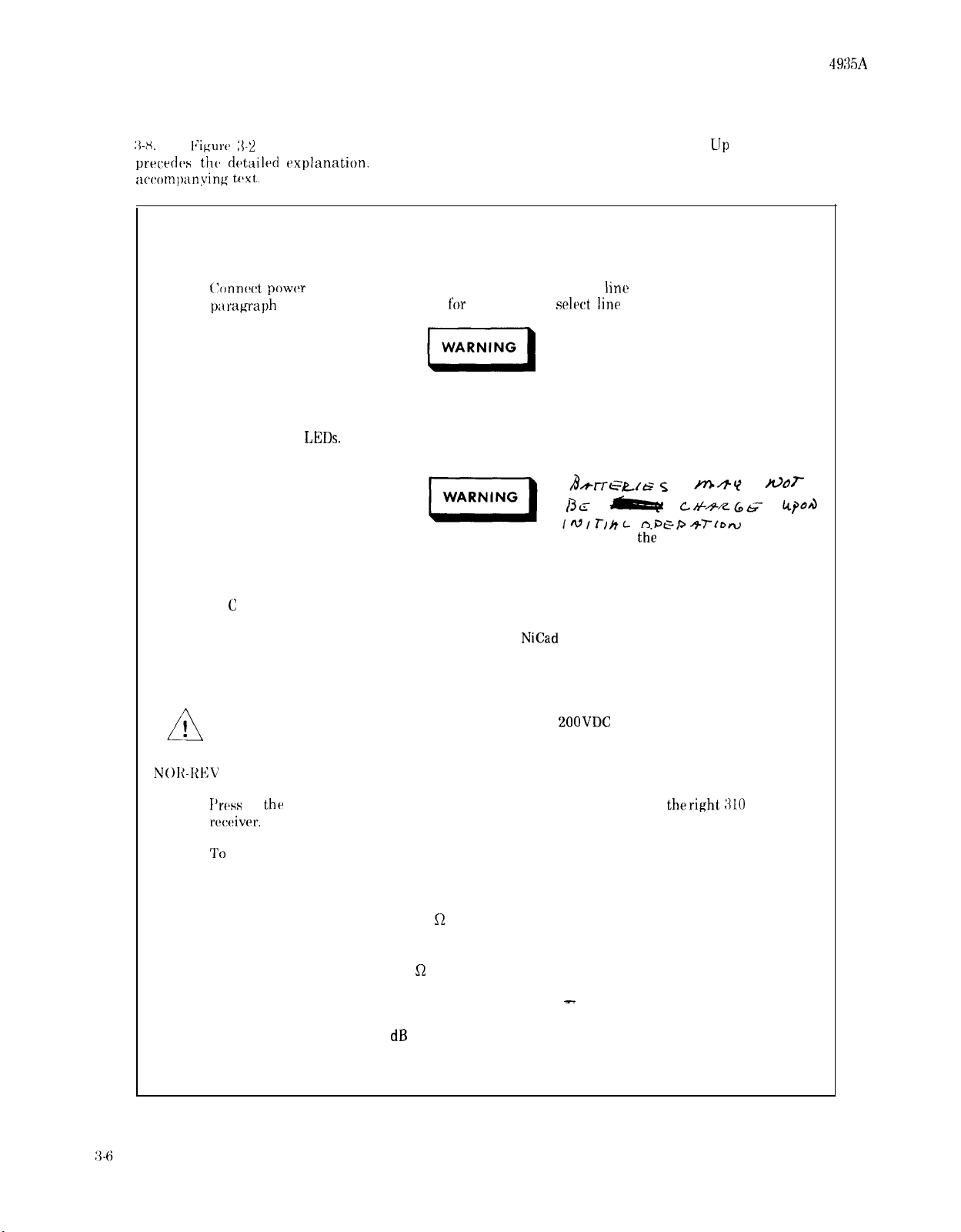
:I-H.
I:inurc :<-2
lists the various measurement modes available. A brief Power On and Set
preccdcs the* dctailcd explanation.
accompanvinfi text.
POWER ON and SET UP
A.C. POWER
1.
(‘onncct power
p;rragraph
2.
Press POWER button ON. The 4935A will automatically do a self check of the transmitter, the
filters, and the
BATTERY POWER (Optional)
1.
Press POWER button ON with no power cord connected. When switching between battery and
A C power cycle the POWER button from STBY to ON again.
cord to the rear line module on which the correct
2-9 of Installation section
Always connect power cord to a properly grounded 3-wire power outlet.
LEDs.
For operator protection during battery operation, connect
terminal on the rear panel to earth ground.
IJp
procedure
Each measurement mode is explained with a drawing and
line
voltage has been selected. See
for
procedure to
select line
voltages.
the
chassis
SET UP
1.
2.
Impedance
1.
2.
NOTE: Proper care in charging and discharging
NiCad
batteries can dramatically improve their
lives. Consult Section I of this manual for recommended procedures.
Connect circuit to 310 jacks. Do not connect more than
BOOVDC
or 10 Vrms at 60 Hz to these
jacks.
I’rcss
in
the
NOR button to connect the left 310 jack to the transmitter and
theright 810
jack to the
recf:iver.
To
reverse the direction of the test press the REV button IN
Press the TRMT impedance button 12 that matches the impedance of the circuit on the TRMT
side.
Press the RCV impedance button $1 that matches the impedance of the circuit on the RCV side. If
the test set is to be used in the bridged mode press the BRG button also. This means that in the
bridged mode two RCV Setup buttons will be pressed in - the correct circuit impedance and the
BRG button. Note: Do not leave the BRG button IN while the instrument is actually terminating
the circuit as it will cause a 6 dB error.
Figure 3-2. Measurements
Page 30
Operation
3-9.
MEASUREMENTS
LEVEL AND FREQUENCY-TRANSMITTER
a.
b.
c.
d.
f’.
Use
MEAS
key to select LEVEL FREQUENCY.
Press
I)ISPLAY-TKMT
can be read in
the
key to display the transmitted signal. TRMT light is ON.
left display and frequency in the right.
I,rvel
If SF signalling units are used on the circuit under test, press SF SKIP key to turn on SF
SKIP. When the light is on the transmitter is blanked from 2450 Hz to 2750 Hz or
?150
Hz around a stored SF SKIP frequency.
SF SKIP frequency is preset at 2600
IIz
(Skip will be 2600 Hz -t 150 Hz). The SF SKIP
center frequency can be changed by putting the desired skip frequency into the
transmitted frequency display. Then press the
to disconnect the transmit side of
the
STORE:
key and the SF SKIP key. He sure
line from the test set first to avoid dropping the
circuit during the storage procedure.
Turn OUTPUT
IXVEI,. I)ATA IXVEI,
sign
indicates the level is >
Use the STEP UP and STEP DOWN keys to set the desired frequency or press
1,EVEL
knob to adjust
is usually
I:( dR
tl:{ dHm.
A - sign indicates the level is < -40
the
level of the transmitted signal to
below the transmission level point
(TI,P).
dHm.
Fl,
I)ATA
A +
F2, F3
or F4 to recall any stored frequency. Holding a finger on either the STEP UP or STEP
DOWN keys causes the transmitter to sweep.
STORE and
and F4 when the
KECALI,
49315A
Frequencies. There are 4 frequencies stored in locations
Fl, F2, F3
is turned on. Fl is 404 Hz, F2 is 1004 Hz, F3 is 2804 Hz and F4 is
271 X Hz. To store other frequencies set the desired frequency in the transmitted frequency
display, press the STORE key and press whichever location key,
Fl, F2, F:%,
or F4 that is
desired as the storage location.
Figure 3-2. Measurements (Continued)
Page 31

Operation
LEVEL AND FREQUENCY-RECEIVER
Model
49315A
a.
b.
c.
d.
Use
MEAS
key to select LEVEL FREQUENCY.
Press
I)ISPI,AY
Read the
A -sign indicates received level is < -78
LEVEL ZERO - For attenuation distortion measurements press LEVEL ZERO key to
set the received level at 0
this point. Pressing the LEVEL ZERO key a second time reverts the level to absolute
units
(dBm)
the reference level per the telephone industry convention.
key to display the
RCV
level in the left display. A t sign indicates the received signal is
dB.
instead of relative units
reckeived
All subsequent level measurements will be made relative to
signal.
dRm.
(dB).
A negative reading indicates levels higher than
The
RCV
light
will come ON
:,+I 3 dRm.
Figure 3-2. Measurements (Continued)
Page 32

NOISE -TRANSMITTER
Operation
a.
b.
Press DISPLAY TRMT-RCV key to display the transmitted signal. TRMT light will be on.
Press
There will be no values displayed because in this configuration the transmitter is turned off and a
quiet termination is supplied to the TRMT jack.
NOISE - RECEIVER
a.
b.
C’.
d.
Press DISPLAY TRMT-RCV key to display the received signal. RCV light will be on.
Press
Press FILTER key to select the desired filter.
Read the
underrange (<0
MEAS
key to select NOISE.
MEAS
key to select NOISE.
dBrn
noise level in the left display. A
dBrn).
“-”
in the left display indicates
Figure 3-2. Measurements (Continued)
Page 33

Operation
4935A TRANSMISSION TEST SET
CB
HEWLETT .
PACK,aRD
I
NOISE WITH TONE - TRANSMITTER
n THRLSH
Model
4935A
n-
a.
1,.
(‘.
Press
MEAS
key to select NOISE WITH TONE.
Press DISPLAY TRMT-RCV key to display the transmitted signal. TRMT light will be on
and 1004 Hz should be in right display.
Turn
OUTPIJ’I’
1 :I dl3
below the transmission level point).
1
XVEI,
NOISE WITH TONE - RECEIVER
a.
b.
C.
Press
MEAS
key to select NOISE WITH TONE.
Press DISPLAY TRMT-RCV key to display the received signal. RCV light will be on.
Read
dBrn
in left display.
Note: Err ‘7 in the right display indicates the received 1004 Hz tone has dropped below
-46
dBm
or exceeded
knob to adjust 1004 Hz signal to data level in left display (usually
+13 dBm.
:3-10
Figure 3-2. Measurements (Continued)
Page 34

A
SIGNAL TO NOISE - TRANSMITTER
Operation
AAAAA
a.
b.
C.
Press
MEAS
key to select SIGNAL TO NOISE.
Press DISPLAY TRMT-RCV key to display the transmitted signal. TRMT light will be on.
Turn OUTPUT LEVEL knob to adjust 1004 Hz signal to data level (usually 13 dB below
the transmission level point).
SIGNAL TO NOISE - RECEIVER
a.
b.
c.
Press
MEAS
key to select SIGNAL TO NOISE.
Press DISPLAY TRMT-RCV key to display the received signal. RCV light will be on.
Read the Signal to Noise ratio as dB in the right display. The received level is displayed in
the left display.
Note: Err 7 indicates the received 1004 Hz tone has dropped below -46
+13 dBm.
dBm
or exceeded
Figure 3-2. Measurements (Continued)
3-11
Page 35

Model
49):2X
4935A TRANSMISSION
HlIWLETT
. PACKARD
TEST
SET
[----I
POWE
I4
IMPULSE NOISE - TRANSMITTER
a.
b.
c.
Press
MEAS
key to select IMPULSE NOISE.
Press DISPLAY TRMT-RCV key to display the transmitted signal. TRMT light will be on.
Press FILTER key to select the same filter as the receiver will use. Although the
transmitted signal is not affected by the filter, selecting either the 15
PROGRAM or 50
tone.
kBit
a
n
kHz
FLAT,
filter will quiet terminate the transmitter instead of sending a hold
d.
‘l‘urn
OIJTPIJT
transmission level point).
LEVEL knob to adjust the level to data level (usually 13 dH below
Figure 3-2. Measurements (Continued)
Page 36

Operation
4935A TRANSMISSION TEST SET
IMPULSE NOISE - RECEIVER
a.
b.
(‘.
Press
MEAS
key to select IMPULSE NOISE.
Press DISPLAY TRMT-RCV key to display the received signal. RCV light will be on.
Press FILTER key to select the appropriate filter.
OUTPUT
d.
Use STEP UP, STEP DOWN and f- + keys to adjust the level of the LOW threshold
shown in the left display. The LOW threshold may be set at any value between 30 and
109
dBrn @ 6OOIl.
Note: Err 8 indicates the threshold is set out of limits. See paragraph 3-6 for limits.
C’.
s.
Press PERIOD key to set the time of the test to 5 MIN, 15 MIN, 60 MIN or NON-STOP.
Press START-RESET key to start the test. The CNTNG LED by the right display will go
on to indicate that the test is in progress. Note that you can see how many counts have
been accumulated at each threshold by pressing DISPLAY key. When NON-STOP is
selected, STOP must be pressed to stop counting.
g.
The left display shows threshold or minutes; the right display shows the number
for the threshold selected.
Note: The 1010 Hz notch filter is automatically used when the C Message or 3
kHz
flat filter is selected, it
is not used for the other filters.
Note: A minus sign in the counts display indicates that the tone has dropped below -46
1
set
during the test. Tone dropout could cause invalid count totals.
dBm
for more than
ofcounts
Figure 3-2. Measurements (Continued)
3-13
Page 37

Opwatiofr
4935A
TRANSMISSION TEST SET
Model 4935A
NOISE TO GROUND - TRANSMITTER (STANDARD UNIT and Option 001)
a.
b.
Press DISPLAY TRMT-RCV key to display the transmitted signal. TRMT light will be on.
Press
MEAS
key to select NOISE-TO-GROUND which provides a quiet termination to the
TRMT jack.
NOISE TO GROUND - RECEIVER (STANDARD UNIT and Option 001)
For valid NOISE-TO-GROUND measurements the test set must be properly grounded. Connect the rear
panel chassis ground post to a known good ground.
a.
I).
c.
d.
Press DISPLAY TRMT-RCV KEY to display the received signal. RCV light will be on.
Press
MEAS
key to select NOISE-TO-GROUND.
Use FILTER key to select the desired filter.
Read
dBrn
noise level in the left display.
Figure 3-2. Measurements (Continued)
Page 38

4935A
&I HEWLETT
TRANSMISSION TEST SET
.
PACKARD
Operation
OTHRESH
I
i
P/AR - TRANSMITTER (Option 002 and 003)
P/AR - RECEIVER (Option 002 and 003)
DIAL
00
a.
b.
(‘.
(‘.
a.
b.
Press DISPLAY TRMT-RCV key to display the transmitted signal. TRMT light will be on.
Press
IJse
P/AR is +3
Press DISPLAY TRMT-RCV key to display the received signal. RCV light will be on.
Press
Read P/AR units in right display.
MEAS
key to select P/AR.
OUTPUT LEVEL knob to adjust signal level to data level. Maximum output for
dBm.
MEAS
key to select P/AR.
A
Figure 3-2. Measurements (Continued)
Page 39

OperatilJn
I)IAI,
and
HOI,11 (WET I)IAI,-III’
DIAL AND HOLD PROCEDURES
and 2 two-wire circuits)
Model
4935A
The ,19:irjA has the
r~xamplr:
pr0c~t~dur.c~
1.
2.
3.
4.
5.
6.
7. If
For 2 two-wire circuits, follow preceding steps 1 through 6 for the first side, then:
1.
2.
3.
I
is as follows:
Connect circuit to left 310 jack.
Push NOR switch to connect TRMT side to left jack.
Conriect the
Push TRMT DIAL switch. Use the butt-in to dial the remote end of the circuit.
After
Push
testing.
the 4935A is designated the receive set, press RCV HOLD switch and then push REV switch to
connect RCV side to left 310 jack.
Push RCV HOLD switch.
Push REV switch to transfer the transmit side.
Push TRMT DIAL switch. Use the butt-in to dial-up the other end.
capability to hold wet dial-up lines (lines where the central office provides battery. For
)])I); I)irect I)istance I)ialing
butt-in handset to the DIAL binding posts.
the circuit is answered, push the TRMT HOLD switch to hold the circuit.
the
TRMT DIAL switch again to release it. This disengages the dial circuitry and allows
network). Dialing can be accomplished with a butt-in. The
4.
5.
After the circuit is answered, push the TRMT HOLD switch to hold this circuit.
Release TRMT DIAL switch by pushing it again.
Figure 3-2. Measurements (Continued)
Page 40

Operation
3-10.
:1-I I.
paragraphs.
transmissicjn.
MEASUREMENT PRINCIPLES
‘I’hc~ principlrs for
Includrd
making mcasuromcnts with the
arc explanations of the
measurcmcnts
and
4Y:GA
are described in the following
the effects
of certain parameters on data
3-12. INPUT-OUTPUT SWITCHING
:i-I :I.
Pressing in the
simultanc~ously
illustratt~cl t)y I’igurch :L‘(.
:1-14.
I)ist.anc~c~ Ijialing:)
test signal
:<-I;,.
impcdanc’e st,lec-ted
obta intd.
:I-l(i.
internal termination provides a resistive load which matches the impedance of the
is
button.
‘I’ho
TKMT and
NOR
button selects the transmit function for the left
performs the receive function. If the REV button is pressed in, the opposite is true as
I’rc*ssing the
without physically changing thr test
‘I’hcs
input and output
‘I’h(h
receive input may he internally terminated or bridged across the circuit under test. The
terminatcbd clxternally,
‘I’hta
bridged
two
circuits.
must match the impedance of the circuit under test, or erroneous measurements will be
mode
IICV
310 jacks provide
IIOI,I)
buttons allows
IJsrd
with the
impcdanccbs
the internal termination is switched out of the circuit by pressing in the
provides a high impedance receive input
NOK
connrction
the 49:GA
and
KI?V huttons
cables
are the standard values of’ I
between thr
to simultaneously hold two
this prrmits changing
and potentially dropping the circuits.
(LTeatrr
49335A
:I10
:S;i, 600,
than 50
and
the
circuit under test.
jack. The right
I)I)T) (Tlirrct
the
direction
or
900
ohms.
line
under test. If
kohms).
310
jack
ofthe
The 49335A
41X15A
the
line
HKG
-RANSMIT/REcEIVE
JACKS
/
1310
e
111
LEFT
JACK
I
TIP
V
RING
A
\
LEFT
DIAL
TRMT
I I
1
x
RIGHT
JACK
RIGHT
TRMT
1
t-Z&
1
I
IIMP:~CE~
RCV
IMPEDANCE
SELECT
TRMT IMPEDANCE
FROM TRMT
OUTPUT
I I
r
RCV
BRIDGE
1 1NOlSETO6
1
XFMR
1
TO
4
l-l
P
1
Figure 3-3. Input-Output Switching
Page 41

Operation
Model
493EA
:;-17.
tlal:ltl(.tad lint,
induc~tancx~,
:i-lH.
itIt lilcl ii,untiset
‘I’hcb ,Il):IT,A
is
t~l~~ctrically
shunt
‘1’0 ;~llow
dialing, talking, and listening on
terminals (binding posts).
input and output circuits are
capacitancca,
symmetrical;
and
the
two sides of’
leakage-tc,-Krounti.
balanced
thca
circuit under test,
3-19. LEVEL AND FREQUENCY MEASUREMENTS
::-“(I.
voic,cs c~h;~nnc~l,
usc~l for :%I1 of theses
‘1%.
IXVKI,
(VARIABLE FREQUENCY
VARIABLE POWER)
TRMT
f+XEI~IJF:NC’Y
1000 f Is loss, frequency
functions.
+pm...+
TIMS
measurement identifies
shif’ts,
and attenuation distortion.
1
TELEPHONE CIRCUIT
)-.. ______-~
-+
to match standard voice channel lines. A
the
line
have
equal series resistance,
th(,
lineman may plug his handset
the
amplitude versus frequency response of’ a
The
setup as shown in
I
l-
dBm
RCV
Figure :3-4
TIMS
series
is
1
Figure 3-4. Level and Frequency Measurements
3-21. 1000 Hz LOSS
:j-22. The
transmitted
data
:1-x1.
circuits. This 4 Hz offset avoids measurement errors caused by test frequencies which are submultiples of
t.hr H kHz “Rarrier”
reason.
1000 Hz loss measurement, determines the point-to-point loss (or gain) of a 1000 Hz test tone
over
a voice channel. To make this measurement, a 1004 Hz test frequency is transmitted at the
level.
At the receiving
The
wakeup transmit frequency is actually
49335A,
the received loss or gain is measured (in
100’1
Hz (not 1000 Hz), to prevent errors over certain
sampling rate. The other preset frequencies
dHm).
F,,
F.,,
and F, are offset for the same
3-24. FREQUENCY SHIFT
3-26. ATTENUATION DISTORTION
:s-27.
:I
circuit using a single frequency measurement technique and defines the circuit’s usable bandwidth. To
make
power is recorded as the reference level at 1004 Hz. Frequencies between 20 Hz and
transmitted. The
attenuation characteristics of the voice channel in
The
attenuation distortion measurement checks the amplitude-versus-frequency characteristics of
th(a mrasurc~ment,
different
a 1004 Hz test frequency is transmitted at the data level. At the receiving
110
power readings may be compared to the
dRm.
1004
Hz reference to obtain the frequency
49XA
the
Hz can be
Page 42

Model 4W5A
Operation
:I-%
of the
0
dli.
The
To obtain loss deviations relative to 1004 Hz, the I,E:VEI,%ERO button is pressed during reception
100.4
I fz reference signal. The received power level is stored (in dHm) and simultaneously displayed as
I,c~vcl
readings taken at other frequencies are compared to the 1004 Hz reference and displayed in
IO04 flz
reference
level
will not have to be subtrartrd from levels at other frequencies to obtain
dH.
dR
readings.
N9.
According to telephone industry convention, attenuation is defined as a change in loss of a
telephone circuit, compared to the loss of a nominal 1000 Hz signal on that circuit. For example, a circuit
with 6
(it%
3-30.
:j-:3 I
th(’
more loss at 2800 Hz would have an attenuation distortion of +6
SF SKIP
SI; Skip (single frequency skip) automatically prevents the
Z450
Hz to 2750 Hz range. This feature is used when transmitting over a dial-up network with single
49XA
dH.
from transmitting frequencies in
frequency signaling units. Any skipped frequency can be programmed using the STORE capability of the
49:K1A (see
Figure
:3-l).
3-32. MESSAGE CIRCUIT NOISE MEASUREMENTS
:x<:i.
Figurtz :(-5
The message circuit noise measurements determine the effects of background noise and tones.
illustrates the basic setup for these measurements.
LINE
MONITOR
(QUIET TERMINATION)
=
))
TELEPHONECIRCUIT
i
)
T
TRMT
TIMS
:%-x4.
The message circuit measurement is obtained by measuring the noise present on a line with a quiet
termination on one end (supplied by the transmitting
end (receiving
:I-35.
4935A).
The C-message filter measures noise signals that annoy the typical telephone service subscriber.
I
Figure 3-5. Message Circuit Noise Measurements
49XA)
Cmessape weighting is also used to evaluate the effects of noise on voice-grade data circuits. C-weighting is
valid for data transmission since the response characteristic is relatively flat over most of the frequency
range for data transmission (600 to 3000 Hz, see Figure
:S-6).
1 RCV
TIMS
1
and a weighted measuring device on the other
3-36.
Hz to 500 Hz) than the C-message filter. By comparing a
The 3 kHz flat filter has a response that provides much less attenuation to the low frequencies (60
3
kHz flat noise measurement to a C-message noise
measurement, the relative influence of low frequency noise (60 Hz commercial power, 20 Hz ringing, etc.)
can he determined (see Figure
Z-7).
Page 43

Operation
Model 49‘EA<r *
r
'
10
0
10
m
0
2
-20
s
s
$
-30
-40
50
60
100
200 500 1000 2000 3000 5000
Figure 3-6. C-Message Weighting Characteristic
-50
6.
100 200 500 1000 3000 4000 6000
Figure 3-7. 3
Frequency
kHz
Flat Weighting Characteristic
(Hz)
Page 44

Model
49:15/I
Operation
:!-:I7
US(YI
‘I’ho
primarily by thr
8).
:xw.
filt.clr,
:<-::0.
‘l’ht~ 15 kHz
1 t
inc~lutles
‘I’ht, 50 kl(it filtelr
101
program
low
g
-30
%
w
-40
cc
weightrd filter
hrondcast
flat
f’ilttbr
is also
t’requrncy noise
is
dcsignrd
is
designed
industry to
for
c~ommunicate hetwrrn
dcsigneti f’or measuremc~nts
in the
measurr~mc~nt (SW Figure :]-$I).
to
mt~asurc~ wcightrtf noise
wcbightd noise mcaasurcments
studio and transmitter site
on program
c~hannrls. I,ike
on wide-band data circuits
on program channels
(SW IJigurr lb
the :3
kHz
flat
(sev b’igurc :S-
-50
-60
0
10
Hz 100 Hz
I
I I
100 200 400 1000
Figure 3-8. Program Weighted Filter
I
FREQUENCY (Hz)
1
kHz
FREQUENCY
I II
10
kHz
I
I
IJ
2000 5000
100
kHz
I
Figure 3-9. 15
kHz
Flat Filter
3-21
Page 45

Operation
-8
m
f
-12
ul
;
-16
w
E
-20
I:“,:
10
100
Figure
IK
FREQUENCY
3-10.
50
kBit
(Hz)
Filter
IOK
50K
Model
4935A
3-40. NOISE MEASUREMENTS
:(-‘I
I.
llt~c~~ivrtl
tomb ;It -90 dllm). For
Whcbn the> (‘-mr~sag:r~
mess;rgc~ wt~ighttd
noise levels are displayed in units
example, a
filter is selected, readings are
measuring
noista
device
is displayed in
reading of 20
displa,ved
ofdlirn,
df3rn
dRm.
or dH with respect to reference noise (1000 Hz
has an
in units
RMS
power of -70
ofdRrn C
and
thenoise Ievc~l
dHm
(20 - 90 = -70).
with a
C-
3-42. NOISE-WITH-TONE (Notched Noise)
:1-4x.
the transmission system to their normal operating levels for continuous data signals. Therefore, noise
Ir~rls art’
:s-44.
At
frequencies between 995 Hz and 1025 Hz are attenuated by 50
passe~l
illustrates the combination of the
combines
3-45.
t3-46.
noise pc,wvr (S
:1-47.
4935A. thta
The remaining received signal (noise) is then compared with the original signal-plus-noise signal. The
computed signal-to-noise ratio is displayed in units of
one or
The noise-with-tone measurement technique is used to condition compandors and/or
received which duplicate levels present under operating conditions.
To
make this measurement, a 1004 Hz test frequency (holding tone) is transmitted at a data level.
the
receiving
through a filter for measurement. The received noise level is displayed in units of
th(s
4935A,
the 1004 Hz holding tone is selectively attenuated by 50 dB using a notch filter (all
(:-message
notch with any of the five filters.
dR).
The remaining received signal (noise) is
weighting and notch filter characteristics. The 4935A
SIGNAL-TO-NOISE MEASUREMENT
‘I’he signal-to-noists
t N/N).
To
make this measurement, a 1004 Hz test frequency is transmitted over the line. At the receiving
1004 Hz signal is selectively attenuated by 50 dH in the notch filter, usually C-message weighted.
the
most important parameters for determining the quality of a line.
mode allows measurement of the ratio of received signal-plus-noise power to
dB.
Figure
:<-I
2 illustrates this measurement. This is
d&n.
quantizers
Figure
:3-l
in
1
Page 46

Model
4’135A
Operation
0
-10
m
0
01
;
x
-20
f
cr
-30
-40
dBm
,004H2
-50
60 100 200
500 1000 2000 3000 5000
Figure 3-l 1. C-Message Weighting with Notch Characteristic
1004 Hz
=
)
)
TELEPHONECIRCUIT
)
dBm
I
SIGNAL + NOISE
,‘,
dB
COMPARE
S-T-N RATIO = 10 LOG
Figure 3-12. Signal-to-Noise Measurement
‘SIGNAL + ‘NOISE
‘NOISE
Page 47

Operation Model
3-48 SINGLE FREQUENCY INTERFERENCE
49:EA
:1-31).
()cc;tsion;tl
t~xampl~~,
Single
frequency interference refers to unwanted steady tones which may appear in lines.
bursts of low level tones which may occur from crosstalk of multifrequency signalling, for
do not fall in this category. Single frequency tones may interfere with certain data signals,
particularly narrowband signals which are multiplexed onto a voiceband channel.
:L-lo
;r(*(*(~t)titt>i(~ I~~vels
c,ltec,k
rnc~s;tgc~ f’iltcbr, t.hc rc~sultant
prc~tlomin;r nl tolls>, wl1ic.h
:i-51.
preserrt
A s~rn~~lcaudio monitorin~~arrangt~mr~ntwill
is
m;~(l~~
are easily
with
h(~;trtl if’thcs C’-mrssagc
the
setup shown in
Figure ;i-5. Af’ter
signal is applied to
may indicate a single
If’s
single frequency tone (or tones) of long duration is heard, single frequency interference may be
usually detect this
noise is within limits,
interf’erencc,
The
single frequency interference
the received noise signal passes through
thclint~monitor spt,~lk(~r.‘l’hr,,Il):(T,A
l’rrqucnc*y intcrf’erencc problem.
since
operator
tonesexceeding
the (:-
listensforany
and should be measured. To determine the frequency and level of the interfering tone, a frequency
selective volt meter or spectrum analyzer must be used. Single frequency interference during a C-message
filter
n~c~asurrmcnt
occurs if the signal is 3 dB or less below the
(:-message
noise limits.
3-52. IMPULSE NOISE
:<-5:<.
Transtent
:1-54.
than
energv.
than
Waveform
impulse
threshold
The
S-level Impulse Noise Mode measures one of the most important transient phenomena.
phenomena can cause data transmission errors and/or interruptions to datacom systems.
Impulse noise is that component of
the
normal peaks of the message circuit noise. It occurs as short duration spikes and/or bursts of
the
received noise signal which is much greater in amplitude
Studies by Hell Telephone laboratories have shown that impulse noise spikes have a duration of less
one
millisecond, and that all significant effects of the noise spike disappear within four milliseconds.
(h)
in Figure
ncjiscs
spikes. The impulse noise measurement counts the number of noise spikes above a selected
level
during a specified time period.
:i-l:i
illustrates a received holding tone (or test signal) that includes interfering
(a)
TRANSMITTED
HOLDING TONE
(bl
RECEIVED
HOLDING TONE
WITH IMPULSE
NOISE SPIKES
I
2
2
TIME
Figure 3-13. Impulse Noise Waveform Representation
Page 48

Model
4W5A
<
t
Operation
3-55.
:I-M.
with reference to ground. The transmitting
channel. and the receiving
NOISE-TO-GROUND MEASUREMENT
The
49XA
uses noise-to-ground to measure the longitudinal noise present on a telephone circuit,
4935A
provides a quiet termination at one end of the voice
4935A
provides a frequency weighted filter and detector at the other end. The
basic measurement technique used for the noise-to-ground measurement is very similar to the message
circuit noise measurement; the main difference lies in the use of a ground reference. Figure
this
dif’fereiice.
:<-14
illustrates
3-57
Noise-to-ground measurements are usually made for troubleshooting purposes; to measure the
magnitude of longitudinal signals, which may indicate the susceptibility of a cable pair to electrical coupling
from external sources. These measurements are also made to coordinate new installations with power
companies, to minimize power line coupling.
:kx.
ground
The relative line balance of an end loop can be calculated by subtracting the measured
(N,)
value from the measured message circuit noise (N.,) value. This calculation is only valid if the
noise-to-
measurements are made on a twisted pair and it is assumed that the message circuit noise is caused by
longitudinal noise converted to message circuit noise by line imbalance. It is recommended that both
message circuit noise and noise-to-ground be measured with the 3
kHz
flat weighted filter to include the
effects of power line related noise.
3-59. PEAK-TO-AVERAGE RATIO MEASUREMENT
3-60.
time of signal amplitude) due to transmission imperfections. As the P/AR signal traverses a dispersive
medium, the peak-to-average ratio will deteriorate. Then by measuring the peak-to-average ratio at the
receiving end, a simple measure of dispersion is obtained. P/AR is measured as the ratio of the peak to
wave rectified average values of a specially processed test signal transmitted over a line. The test signal has
a peak-to-average ratio and a spectral content that approximates a data signal. Figure
frequency spectrum of the transmitted P/AR test signal, and Figure 3-16 illustrates the signal envelope.
The
4935A
uses the peak-to-average ratio (P/AR) to measure the channel dispersion (spreading in
315
illustrates the
full-
Page 49

A E 1140.625
0
10
m
3
:
2 20
r:
x
fi
10
40
Model 4935A
KEY FREQUENCY
A 140.625
8
c
[I
G 1640.625
J
390.625
640.625
890.625
F
1390.625
H
1890 625
I 2140 625
2390.625
K 2640 625
L 2890 625
M
3140 625
N 3390.625
0 3640.625
P
3890.625
5o
A--
BCDEFGHIJKLMNOP-
.joo
2000 3000
Frequency
(Hz)
Figure 3-l 5. P/AR Transmit Signal Frequency Spectrum
w
0
2 4 6 8
Time (mSI
Figure 3-16. P/AR Transmit Signal Envelope
Page 50

Model
49’ISA
%
I
:i-6
1.
The
P/‘AR
measurement is a single number rating of the fidelity of a voiceband channel and is a
weighted measure of the total attenuation, phase distortion, and noise. The P/AR rating is derived by
comparing the P/AR of an ideal signal with the P/AR of the output signal of the system under test. The
P/AR
measurement is most sensitive to envelope delay distortion and is also affected by noise, bandwidth
reduction, gain ripples, nonlinearities such as compression and clipping, and other impairments. P/AR is
simpler to understand than envelope delay because it is only one number instead of a curve. Also P/AR can
be measured in loop-around mode with only one instrument, unlike envelope delay. If the P/AR signal were
received
the
entirely undistorted, the
pea k-to-;rveragc
ratio has a
R/AR
rating would be
P/AK
rating of 80.
100.
while a circuit that causes a
10%
reduction in
Operation
:M2.
particular case. However, since P/AR is a figure of merit for the channel, it can be used as a benchmark for
future reference. After other measurements are made and a channel is considered acceptable, the P/AR
rating can he recorded for future reference. In case of a suspected trouble on the channel, P/AR may be
measured first and he compared to the benchmark P/AR value. Deviations in excess of +4 P/AR units from
an initial P/AR value provides sufficient reason to suspect that some channel characteristic has changed
significantly.
‘I’hc P/AR
measurement provides little information about the nature of the fault condition in any
3-27/(3-28
blank)
Page 51

Page 52

Model 49:GA
4-l. INTRODUCTION
Performance Tests
SECTION IV
PERFORMANCE TESTS
4-2.
inspection and can be done without accessing the instrument’s internal circuits. If the instrument fails the
tests, refer to the Service Section.
Tests in this section verify instrument specifications. These tests may be used as part of incoming
4-3. EQUIPMENT REQUIRED
4-4.
characteristics may be substituted.
Kquipmrnt required for the performance tests is listed in Table 1-2. Test equipment with similar
4-5. TEST RECORD
4-6.
recorded during incoming inspection can be used for comparison in maintenance, troubleshooting, and
following repairs and/or adjustments.
Test results may be recorded on the test record located at the end of this section. Results of tests
4-7. SELF CHECK
4-x.
arc tested in addition to all the front panel leds and seven segment displays.
4-9. PERFORMANCE VERIFICATION
4-10.
environment, the instrument should be checked every six months using the performance tests. Performance
tests should also be made following repair or when internal adjustments are required.
4-l
totally confirm that the instrument meets the published specifications. Perform the full test to verify that
instrument’s performance completely meets the specifications.
Self check is automatically done each time the instrument is powered up. Some circuits and filters
This instrument requires periodic performance verification. Depending on use and operating
1,
To shorten testing time, the abbreviated Performance Tests may be used. The test results do not
4-1
Page 53

4-12. PERFORMANCE TESTS
PERFORMANCE TESTS
4-13.
Sfc’l’l
Transmitter Flatness at
‘I’:
MODEL 4935A
+lO dBm
COUNTER
I
BNC
ADAPTER
Figure 4-l. Transmitter Flatness Test at
1
A
00
VOLTMETER
-
0 000
+lO dBm
ncl
0
1.
:1
4.
5.
ti
Fluky 52OOA
f I I’ .X 15
fI f’ :{49OA
L!(J df3
Figure
(‘onnect
AC
(:alihrator
C’ounter
Multimetrr
Amp (circuit shown in
4-l:])
Voltmeter to
f’OWF:R_. .
I)ISI’I,AY_,
SET 111’
MEASITREMEN’I’_.
Stst t.ht, .49):i5A
A(lj\lst 49:l:iA
to 1004 Hz
OIJ’I’I’lJ’l’
L’l~limetrr (notcx: 4935A
(‘t1(a(,k
the
49:GA
transmitter at the frequencies listed in
Ai, X,i kHz
;Irld
X5.004
verify that the
kHz.
HNC
to 310 adapter
2 HNC
cables
f3NC
“‘I”’ connectors
600
ohm termination
I
f3NC
to
the 49:GA TRMT
I,E:VEI,
jack as shown in
until
2.4:35
_,
I,EVEI,
Vrms (9.95
must be terminated as shown above.
49:ISA
frequency when measured with the counter is between 84.996
banana cahlr
Figure
4-l
_,
press in TRMT
_.
_.
ON
TRM’I
CiOOU
E‘REQIJENCY
d&n
into 600 ohms) appears on the
Table 4-I
kHz
4-2
Page 54

Model
49:15A
Performance Tests
PERFORMANCE TESTS
Table 4-l. Transmitter Flatness at
ACCEPTABLE VOLTAGE RANGE
AHHREVIATEI)
FREQUENCY
20 Hz
200
Hz
5
kHz
15
kHz
30
kHr
TRANSMITTER FLATNESS AT
See the Abbreviated Transmitter Flatness Test.
+lO dBm
2.17 to273 Vrms
2 38 to249
2 38 to249
2.38 to249 Vrms
2 30 to258
2 30
to 2
2 25 to264
+10 dBm
TEST
58
Vrms
Vrms
Vrms
Vrms
Vrms
4-3
Page 55

PERFORMANCE TESTS
Model
49:GA
4-14.
SE’I’I
Transmitter Flatness at -40
I I’:
MODEL 4935A
m-1
AC CALIBRATOR
Figure 4-2. Transmitter Flatness Test at -40
IJlukc 52OOA AC (:alibrator
I 20 dH amplifier
111’ W14A l)uul
(set:
figure
Output
4-I ii)
Power
dBm
Supply
VOLTMETER
I
0
OOOQQ
dBm
:1
IO to banana adapter
2 banana plug test cables
HP :349OA
Multimeter
on
2.
ii.
I’OWEI~
I)ISI’I AY
L 1
NOR
SET
IJl’
.
MISASIJREMENT
Adjust
!+st t,hr
<I.
IMPIJI,SE
the l’ower
AC Calibrator and the
Set
the
NOISE
Supply to
A(:
Calibrator to 7.746 mV (-40
floating.
I).
(‘onncct thta
AC
voltage.
(’
(‘onnect the t20 dH
output with the voltmeter.
(1.
Adjust
th(l 49:GA
1 20 dH
f>xactly
NOTIC:
amplifier
-40
A 600 ohm termination is provided by the
dHm.
Service Kit and must be added if a high impedance amplifier is used.
. . . . . . . ..I........... ON
. . . . . . . . . . . . .
press in TRMT
HRG out
DIAL
both
HOI,I)s
I,IWE:I, F’REQUENCY
provide -t 12
49:EA
(:alibrator
V to
to exactly -40
to the
amplifier input to thr
OIJTI’U’I’
LIWEI,
iress I)ISPI,AY
the
t20
dH
Amplifier
dRm
as follows.
dRm
into 600 ohms) at 1004 Hz with
t20 dH
amplifier input. Record the amplifirr output
49XA
TRMT 310 jack. Monitor
control until the voltmeter reading is the same as the
(1004 Hz)
output voltage in step b. The AC Calibrator and the
t20
dR
amplifier in the
TRM’I
press
49XA
In
60011
out
out
the +20
are both set to
the
output
amplifier
IXagnostic
3-4
Page 56

PERFORMANCE TESTS
Performance Tests
(in
Vout
mV)
‘4.
5.
6.
7.
8.
110
not change -40
dHm
setting on the AC Calibrator or the
49%A OlJTPUT LEVEI,
settings
during the rest of this test.
Connect the AC Calibrator to the
Set the AC Calibrator to 20 Hz.
:i.
Record the voltage.
b.
C’.
From Table 4-2 locate the horizontal voltage line closest to the recorded voltage reading. Use
$20 dH
amplifier input.
this voltage line (see example).
EXAMPLE:
If the Voltmeter reading is 71.0
mV,
locate the 71.0 mV line from the
V,,,,t
column of Table 4-2. Locate the 20 Hz frequency column. The allowable
voltage reading, when the AC Calibrator is substituted by the
transmitter, is 79.7 mV to
Substitute
I)( )WN
Ido
From
the
4935A
TRMT output in place of the AC Calibrator.
buttons in conjunction with the - or -buttons to set the 4935A TRMT frequency to 20 Hz
not adjust the OUTPUT LEVEL).
Table 4-2, locate the voltage line identified in Step 3. In the vertical frequency column
63.S mV.
LJse
the STEP UP or STEP
4935A
(frequency under test) identify the allowable voltage range. Verify that the +20 dR amplifier output
is in this range.
Repeat Steps:1to 5
+I.0 dB
20 Hz
for each frequency column of Table 4-2
Table 4-2. Transmitter Flatness at -40
iO.2
dB
200 Hz
kO.5
dB
50 Hz
& kO.2
dB
15
kHz
(20 Hz through 85 kHz).
dBm
irO.5
dB
60
kHz
-i-O.5
dB
85
kHz
65 0
65 4
65.8
66 2
66 6
67 0
67 4
67 8
68 2
68 6
69.0
69 4
69.8
70.2
70 6
71 0
71 4
71 8
72 2
72 6
73 0
73 4
73 8
74.2
74 6
72.9 to 57 9 68 9 to 61.4 66 5 to 63 5
73 4 to 58 3 69 3 to 61.7 66 9 to 63 9
73 8 to 58 6 69 7 to 62.1 67 3 to 64 3 69 7 to 62 1
74.3 to 59.0 70.1 to 62 5 67.7 to 64 7
74 7 to 59 4 70 5 to 62 9 68 2 to 65 1 70 5 to 62.9
75 2 to 59 7 71 0 to 63 3 68 6 to 65.5 71 0 to 63 3
75 6 to 60 1 71.4 to 63.6 69 0 to 65.9 71 4 to 63 6
68 9 to 61 4
693to61
7 69.3 to 61.7
68.9to61 4
69.7 to 62.1
70 1 to 62 5 70.1to62.5
70 5to 62 9
71 0to 63.3
71 4to 63.6
761 to604 71 8 to 64.0 69 4 to 66 3 71 8 to 64.0 71 8to 64.0
76 5 to 60 8
77 0 to 61 1 72.7 to 64.8 70.2 to 67 0 72 7 to 64 8
722to644
69 8 to 66 6
722to644
72.2 to 64.4
72.7 to 64 8
774 to 61.5 73 1 to 65.1 70.6 to 67 4 73 1 to 65.1 73.1 to 65 1
77 9 to 61 9 73.5 to 65 5 71 0 to 67 8
73 5 to 65.5 73.5 to 65.5
78 3 to 62 2 73.9 to 65.9 71 4 to 68.2 73 9 to 65.9 73.9 to 65.9
78 8 to 62 6 74.4 to 66.3 71.8 to 68.6 74 4 to 66 3
74.4 to 66.3
79 2 to 62 9 74.8 to 66.7 72 2 to 69 0 74 8 to 66 7 74.8 to 66 7
79 7 to 63 3 75 2 to 67.0 72.7 to 69 4 75 2 to 67 0 75.2 to 67.0
80 1 to 63 6 75 6 to 67 4 73 1 to 69 8 75.6 to 67 4
80 6 to 64 0 76 1 to 67 8 73.5 to 70.2 76 1 to 67.8
81 Oto643 76 5 to 68 2 73.9 to 70.6
76 5 to 68.2 76.5 to 68.2
81 5 to647 76 9 to 68 5 74 3 to 70 9 76 9 to 68 5
75.6 to 67.4
76.1 to 67 8
76 9to 68.5
81 9 to 65 1 77 3 to 68 9 74.7 to 71 3 77 3 to 68 9 77.3 to 68.9
82 4 to 65 4 77 7 to 69 3 75.1 to 71 7 77 7 to 69 3
82.8 to 65 8 78.2 to 69.7 75.5 to 72.1
83 3 to 66 1 78.6 to 70 0 75.9 to 72.5
83 7 to 66 5 79.0 to 70.4 76 3 to 72 9
78 2 to 69.7 78.2to69.7
78 6 to 70.0 78.6 to 70.0
79oto704
77.7 to 69.3
79.0 to 70.4
4-5
Page 57

PERFORMANCE TESTS
Table 4-2. Transmitter Flatness at -40
Vout
(in
mV)
750
754
758 /
762 85 5 to 67 9 807 to71 9 78 0 to 74 5 80 7 to 71 9
766 i 85 9 to 68 3 81 1 to 72 3 78 4 to 74 9 81 1 to 72 3 81 1 to 72.3
‘l.OdB20Hz
-
1 84 2 to 66 8 79 4 to 70 8 76 7 to 73 3 79 4 to 70 8 79 4 to 70 8
84660672
:
85
0 to 67 6
86
4 to 68 6 81 6 to 72 7 78 8 to 75 2 81 6 to 72 7 81 6 to 72 7
86 8 to 69 0 82 0 to 73 1 79 2 to 75 6 82 0 to 73 1 82 0 to 73 1
87 3 to 69 3 82 4 to 73 4 79 6 to 76 0 82 4 to 73 4 82 4 to 73 4
87 7 to 69 7 82 8 to 73 8 80 0 to 76 4 82 8 to 73 8 82 8 to 73 8
88 2 to 70 1 83 3 to 74 2
88 6 to 70 4 83 7 to 74.6 80 8 to 77 2 83 7 to 74 6 83 7 to 74 6
89 1 to 70 8 84 1 to 75 0 81 2 to 77 6 84 1 to 75 0 84 1 to 75 0
89 5 to 71 1 84 5 to 75 3 81 7 to 78 0 84 5 to 75 3 84 5 to 75 3
90 0 to 71 5 85 0 to 75 7 82 1 to 78 4 85 0 to 75 7 85 0 to 75.7
90 4 to 71 8 85 4 to 76 1 82 5 to 78 8
90
9 to 72 2 86 8 to 76 5 82 9 to 79 2 85 8 to 76 5 85 8 to 76 5
91 3 to 72 5 86 2 to 76 8 83 3 to 79 5 86 2 to 76 8 86.2 to 76.8
91 8 to 72 9 86 6 to 77 2 83.7 to 79 9 86 6 to 77 2 86 6 to 77 2
9% 2 to 73.3 87 1 to 77.6 84 1 to 80 3 87 1 to 77 6 87 1 to 77.6
92 7 to 73 6 87 5 to 78 0 84 5 to 80.7 87 5 to 78 0 87 5 to 78.0
-1~0.5 dB
50 Hz
79 9 to 71 2 77 2 to 73 7 79 9 to 71 2 79 9 to 71 2
803to71
6 77 6 to 74 1 80 3 to 71 6 803 to71 6
fO.2 dB
& to.2 dB
804to768
dBm
200 Hz
15
kHz
(Cont’d)
LO.5 dB
60
kHz
83 3 to 74.2 83 3 to 74 2
854to76.1
i0.5 dB 85
807to71
85 4 to 76 1
kHz
9
93 1 to 74 0 87 9 to 78 4 84 9 to 81 1 87 9 to 78 4 87 9 to 78 4
93 6 to 74 3 88 3 to 78 7
94 0 to 74 7 85 8 to 81 9 88 8 to 79 1
94 5 to 75 0 89 2 to 79 5 86 2 to 82 3 89 2 to 79 5 89.2 to 79 5
94 9 to 75 4 89 6 to 79 9 86 6 to 82 7 89 6 to 79 9 89 6 to 79 9
9!i
4 to 75 8 90 0 to 80 2 90 0 to 80 2 90 0 to 80 2
95 8 to 76 1 90.5 to 80 6 87 4 to 83.5 90 5 to 80 6 90 5 to 80.6
96 3 to 76.5 90 9 to 81 0 90 9 to 81
96 7 to 76 8 91 3 to 81 4 88 2
97 2 to 77 2 91 7 to 81 8 88 6 to 84 6 91 7 to 81 8 91 7 to 81 8
97 6 to 77.5 92 2 to 82.1 92 2 to 82 1
98 1 to 77 9 92 6 to 82 5 92 6 to 82 5
98 5 to 78 3 93 0 to 82 9 89 8 to 85 8 93 0 to 82 9 93 0 to 82 9
99 0 to 78 6 93 4 to 83 3 90 3 to 86 2 93 4 to 83 3 93 4 to 83 3
99 4 to 79 0 93 8 to 83 6 90 7 to 86 6 93 8 to 83 6 93 8 to 83 6
99 9 to 79 3 94 3 to 84 0 91 1 to 87 0 94 3 to 84 0 94 3 to 84 0
100 3 to 79 7 94 7 to 84 4 91 5 to 87.4 94 7 to 84.4 94 7 to 84.4
1008 to800 95 1 to 84 8 91 9 to 87 8 95 1 to 84.8 95 1 to 84.8
101 2 to804 95 5 to 85 2 92 3 to 88 1 95 5 to 85.2 95 5 to 85 2
101
7to807
102 1 to 81 1 96 4 to 85 9 93 1 to 88 9 96 4 to 85.9 96 4 to 85.9
96 0 to 85 5 92 7 to 88 5 96 0 to 85 5 96 0 to 85 5
853to81
5 88 3 to 78 7 88 3 to 78.7
.O
t0
a4 2 91 3 to 81 4 91 3 to 81 4
90 9 to 81 0
4-6
Page 58

PERFORMANCE TESTS
ABBREVIATED TRANSMITTER FLATNESS TEST
Pcrformancc Tests
2.
_.
4.
5.
I.
USC test
SCI
setup
up
the 403SA as hollows:
shown in
Figure
4-2.
POWER -ON
DISPLAY - TRMT
NOR - press in
SET UP -
BRCi
DIAL
out
0111
press
in TRMT 600
both HOLDS out
MEASLIREMENT -
1
Se1 Ihe 4935A
lo
Adjust the OUTPUT LEVEL until
Cheek the 4935A transmitter
LEVEL FREQUENCY
IOO4Hz.
at
the
0.775V(O dBm) appcors
frcqucncics
given
in
on
Table
the
Voltmctcr.
4-3.
Table 4-3. Abbreviated Transmitter Flatness
VOLTAGES (VRMS)
FREQUENCY MIN MAX
20 Hz
200 Hz
15
kHz
85
kHz ,731
,690 ,869
,757 ,793
,757
,793
,820
1lOkHz ,652 ,920
4-7
Page 59

Performance
‘r&s
Model 4935A
PERFORMANCE TESTS
4-15.
SEW Jl’:
RECEIVER ACCURACY at
AC CALIBRATOR
r
-.
Figure 4-3. Receiver Test at + 11 dBm and -40 dBm
Fluke
5ZOOA
AC Calibrator
111’53
I5
t’rcc~llcncy (‘oulltcl~
1{10
to
BNC
adapter
HN(: “1”’
+ll dBm
COUNTER
and -40
dBm
BNC‘T’
3
BNC cables
2 BNC to banana cables
1 banana plug cable
MODEL 4935A
1.
2.
(‘onnect
the AC Calibrator to the
Setup the 4935A as follows:
POWER
I)ISI’I
AY
L 1
REV . . . . . . . . . . . . . . . . .
SET
1JP
MEASUREMENT
RfiZ(‘151Vl2K A(:CIJRACY
1.
2.
Set ,2(: Calibrator output to 2.733 V (+10.95 dBm into 600 ohms; the0.05 dB offsetchecksfor round
off
errors
in the
The 49XA
level and frequency displays should be within the limits shown in Table 4-3.
Rti:(:I~:IVER A(:CIJRACY
I.
2.
Set,
the AC Calibrator output to 7.702 mV (-40.05
‘I’hc 49:35A
level display should be within the limits shown in Table 4-4.
.
.
AT
+11 dBm
4935A).
AT
-40 dBm
4935A
RCV jack as shown in Figure 4-4.
I
.
.
.
. . . . . . . . . . . . . . . . . . . .
. . . . . . . . . . . . . . . . .
ON
RCV
. press in
.
press in RCV 6000
press in BRG
LEVEL FREQUENCY
dBm
into
600
ohms).
4-x
Page 60

Model 4935A
PERFORMANCE TESTS
Table 4-4. Receiver Accuracy Test Table
FREQUENCY
(MONITOR FREQUENCY
AT COUNTER) tll DBM -40 DBM
20
Hz
50 Hz 105 to 11 4
200 Hz
500 Hz
1000 Hz
5000 Hz 10.8 to 11.1
15000
Hz
30000 Hz 105to 114
50000 Hz 105to 114 -40.5 to -39.6
85000 Hz 10.5 to 11.4 -40.5 to -39.6
110000
Hz
loot0
11 9
10.8to
11 1
108to
11.1
109t0110
10.8 to 11.1
goto
129 -42 0to~38.1~ i.01
-41
0to -39 1
-40.5 to
-40
-40 2 to -39.9
-40
-40
-40 2 to -39.9
~40.5
-39
2 to -39 9
2 to -39 9
2 to -39 9
to -39.6 + 01
6
TOLERENCE
il
Hz
-tl
Hz
il
Hz
:il
Hz
-tl
Hz
i-1
Hz
+l
Hz
k.01 kHz
i.01
Performance Tests
kHz
kHz
kHz
AHHRE:VIATEl1
1.
2. Stlt
LJse
the test setup shown in Figure
the AC Calibrator to
Test the
RECEIVER ACCURACY TEST
4-:3.
.7791
V (-0.05
4935A
at each frequency given in Table
Table 4-5. Abbreviated Receiver Accuracy Test Table
FREQUENCY (0.7791
20 Hz
50 Hz
200 Hz -0.2 to +0 1
15
kHz
85
kHz
110kHz
~1
0 to +0 9
~0.5
-02to+Ol
-0.5 to +0 5
-2 0 to tl 9
dBm
into 600 ohms).
4-5.
LEVEL FREQUENCY
to t04
V)
dBm
dBm
dBm
dBm
dBm
dBm*
TOLERANCE
21
Hz
fl
Hz
+l
Hz
i
01
kHz
2.01 kHz
2.01 kHz
*For instruments with serial prefix
inf’ormation.
2207A
and below refer to Section VII Manual Changes backdating
4-9
Page 61

Pdormance ‘I’c~sts
4-16. Autorange Test
AC CA
LIBRATOR
PERFORMANCE TESTS
Figure 4-4. Autorange Test
MODEL 4935A
Model
49’35A
.tt
1.
2.
:i.
I”luk(l 52OOA A(:
Calibrator
1 banana plug test cable
I BNC
to
bantina
adapter
(:onnect.
equipment as shown in Figure 4-4. On
POWER
r)rsI'I~AY':::::::::::::::::::::::::::::::::::::::::::::::::::::::::'R(:V
SW IJP
MEASI!KEMENT
St t,he A(: (:alibrator
l+‘clr tbach
voltage and range in Table
. . . . . . . . . . . .press
.
to 1000 Hz.
4-6
check that the display is within acceptable limits.
Table 4-6. Autorange Test
AC
CALIBRATOR
VOLTAGE DISPLAY
-
i
86911 V
086911 V 191 to -189
0086911 V 39.2 to -38.8
00086911 V 594to
2 7484 V
0 27484 V 91 to- 89
0.027484 V
0.0027484 V
I,EVEI,
+09to
4935A
1~10.9
292to-288
49 4 to
select:
to
+1
---48.6
ON
RCV (iOOf2
FREQIJENCY
+11
~586
1.1
4-10
AHHKEVIA’I’EI) AIJTORANGE
Thrw
is no
;~hhrc+ated
Autorange Test.
TEST
Page 62

Model
4935A
Performance Tests
PERFORMANCE TESTS
4-17.
Filter Tests
SETUP:
,
EQI JIPMENT:
Fluke
I
BNC
I
BNC
GENERA12
1.
PROCEDURE
Connect equipment as shown in Figure
AC CALIBRATORAC CALIBRATOR
52OOA
AC Calibrator
to dual banana test cable
to
310
adapter
MODEL 4935AMODEL 4935A
Figure 4-5. Filter TestsFigure 4-5. Filter Tests
4-5.
2.
3. On
Set AC Calibrator to
4935A
select:
POWER
DISPLAY . . . . . . . . . . . . . . . . . . . . . . . . . . . . . . RCV
SETUP
MEASUREMENT
FILTER . . . . . . . . . . . . .
C-MESSAGE FILTER
1.
2.
Select the C-MESSAGE filter on 4935A.
Check the response at each frequency in Table 4-7. The 4935A should be within the range given
,775
V (0.0
dBm
across 600 ohms)
. . . . . . . . . . . . . . . . . . . . . . . . . . . . . . . .
. . . . . . . . . . . . . . . . . . . . . . . . . .
RCV
. . . . . . . . . . . . . . . . . . . . . . . . . . . . . . .
select according to test
Table 4-7. C-Message Filter Test
FREQUENCY RECEIVED LEVEL
(in Hz) ACCEPTABLE READINGS
(dBrn)
300 73-74
900 89-90
1000
2500
3000
90
88-89
87-88
4500 66-71
ON
60011
NOISE
4-11
Page 63

I’erformanct~ ‘I’c~t,s
:I
kIl% FI,A’I’ FIl,‘l‘ER
(‘h~k
giWl1.
the
TEST
rcasponse
PERFORMANCE TESTS
at each frequency in
Table4-8.
The
4935A
display should be within the range
Model
49‘Ii’A
I
T 1
Table 4-8. 3
FREQUENCY
1
2
S;c*l~~ct
tho I5
kHz PI,AT
(7l~c.k the responsc~
Filter on the
at
each
frequency in Table
kHz
Flat Filter Test
RECEIVED LEVEL
ACCEPTABLE READINGS
90
86-88
75-80
(dBrn)
4935A
4-9. The 49XA
display should 1~ within tho range
given.
Table 4-9. 15
FREQUENCY RECEIVED LEVEL
(in Hz) ACCEPTABLE READINGS
1000 90
15000
30000
kHz
Flat Filter Test
86-88
75-80
(dBrn)
4-l”
F’RO(;RAM I”II,‘l’ER
1.
2.
S&ct the
( ‘hrck
PROGRAM filter on the
the response at each frequency in Table 4-l 0. The
given.
TEST
49XA.
Table 4-10. Program Filter Test
FREQUENCY
(in Hz)
100 62-65
500 83-84
1000 90
2000 94-95
5000
10000 78-85
RECEIVED LEVEL
ACCEPTABLE READINGS
95-98
4935A
display should be within the range
(dBrn)
Page 64

Model 4035A
50
ItBIT
FILTER TEST
PERFORMANCE TESTS
Performance
Tests
I. Sclcct
2. Cheek the
the
SO
rcsponsc at
range given.
NOTCH FILTER TEST
I. Sclcct the
I5
kBlT Tiltcr
on the
4935A.
each lrcyucncy
in
Toblc
NOTE
Test
must bc
Table 4-11. 50
FREQUENCY RECEIVED LEVEL
(in Hz)
1000 90
15000 89-90
25000
35000 84-86
50000
kHz Cltcr
and NOISE WITH TONE
pcrformcd
in
sccluencc given.
kBlT
Filter Test
ACCEPTABLE READINGS
87-88
62-67
4-l I.
The 493SA
(dBrn)
mcasurcmcnt
display should bc within the
on
the 4935A.
2.
Cheek the
rcsponsc at
given.
FREQUENCY RECEIVED LEVEL
(in Hz)
At 400 tlz
the
DISPLAY FREQUENCY will not bc stable.
ABBREVIATED FILTER TEST
Thcrc is no
abbrcviatcd Filter Tat.
each frcclucncy
in
Table 4-12. The 4935A
Table 4-12. Notch Filter Test
ACCEPTABLE READINGS
400
862
1000
1020
1182
1700 90
90
288
<40
<40
288
NOTE
(dBrn)
should bc within
the range
4-13
Page 65

Performance
4-18. IMPULSE NOISE DAC TEST
5tc’1’1’1’-
Tests
PERFORMANCE TESTS
Model
49XA
AC CALIBRATOR
Figure 4-6. Impulse Noise DAC Test
MODEL 4935A
h‘luke 52OOA AC: (:alibrator
1
HN(:
to dual banana test cable
I
:110
to
HNC
adapter
I.
2.
( ‘onnect
()I1 lcxiT,A w1ect:
equipment as shown in Figure
POWISK
4-6.
. . .
ON
I)ISI’I,AY_. RCV
SET
IJI’
. press both
MEASIJREME:NT
h’II,TER
IMI’IJLSE
NOISE . . . . .
. . . .
press
press
PER1011
I)ISPI,AY
to select NON-STOP
to select
6OOb2
buttons
IMPULSE NOISE:
16
kHz I;I,AT
Filter
I,OW(SET)
press START/RESET
Left
display . . . . .
adjust threshold to 90
d&n
4-14
:I.
4.
5.
6.
7.
H.
9).
10.
11.
1%.
I:{.
14.
Set AC
The 4!):(5A
K;rise
The
Kepeat
Set the
I’ress IjlSPl,AY
Set the
Set the
I’ress 1)ISPLAY
Set the
Set the AC Calibrator to 1.457 V; the
(L~librator
signal source to 2
kHz
at the levels given in Table 4-l 3 (start with 0.580
should start counting.
the
49:35A lL)W THRESHOI,I) HY 1 dHrn.
4!):{5A
display should stop counting,
steps :I through 6 for each level shown in Source in Volts Table
LOW(SET)
A(: (Ldibrator
A(:
Calibrator to 0.920 V; the
A(:
Calibrator to
threshold to 90
in
IMPUI,SE
to 0.820 V; the
in IMPULSE:
I.299
dRrn
(0
dHm).
NOISE to select
4!):<5A
4935A
display should count.
NOIEX
to select HIGH threshold.
V; the
41135A
display should not count.
4935A
display should count.
MI11
threshold.
display should not count.
V)
4-I:].
Page 66

Model
493A
PERFORMANCE TESTS
Table 4-13. Impulse Noise DAC Test
AC CALIBRATOR PEAK SIGNAL COUNTING NOT COUNTING
VOLTAGE IN
dBm
THRESHOLD THRESHOLD
Performance Tests
0 580 05 90
0651
0 730
0 820
0.920
1 032
1158
1 299
1.457
1.635
L
AHHKEVIATED IMPUISE
NOISE DAC TEST
1.5 91
2.5
3.5
4.5
55 95 96
65 96 97
7.5
85 98 99
9.5
There is no abbreviated Impulse Noise DAC Test.
91
92
92 93
93 94
94
97 98
99
95
100
4-15
Page 67

I’rrf’ormancc~ Tests
Model
4935A
-___-
4-19. Count Limit Test
AC CALIBRATOR
EI)IJIPMP:NT:
Flukr :P%OOA A(: (:alibrator
I bzmana
I :1 IO to banana adapter
1.
(‘onnect
plug test cable
equipment as shown in Figure 4-7.
PERFORMANCE TESTS
MODEL 4935A
Figure 4-7. Count Limit Test
2.
POWER_. . . .
I)ISPI,AY
. .
Mb:ASlJFtEMENT_.
3.
‘1.
5.
fi.
8.
9.
IO.
1
Stst AC (2rlibrator
Adjust
Press the
L% ai t, 60
I’ress Impulse
‘I’hch l!XEA
I’rcss I)ISI’IAY butt.on
I.
‘l’h(~ 49:15A
PII,TP:R
IMI’IJI,SF:
the 49:%A
seconds and press STOP.
. . . . .
NOISE
to 2000 Hz,
threshold to 75
STAII’I’/KESF:T
Noise
I)ISPI,AY
display should indicate 480
display should indicate 480
Al3HIZE:VlA’l’F:I) (:OlJNT I,IMTT
‘I’htarti
is no abbreviated Count
I,imit
.
button.
in
TEST
,775
V (0.0
d&n.
button to
IMPIJLSE
Test.
_.
The 4935A
lf-48
_.
dHm
into
600
_.
ohms).
IMPIJISE
right display should indicate 480
selrct MI11
threshold.
counts.
NOISE to select HIGH threshold.
_iilH
counts.
NOISE:
:I
kHz
FLAT
I,OW(SET)
ON
KCV
+48
counts.
4-16
Page 68

Model 4935A
4-20. Termination Impedance Test
EQIJII’MENT:
PERFORMANCE TESTS
MODEL 4935A
I
310 TO BNC
4
BNC TO DUAL BANANA
llli
lza
Figure 4-8. Termination Impedance Test
TEST RESISTOR
9OOf1, 6OOf1
or
13512
Performance Tests
1.
2.
3.
4.
5.
HP 3490A Multimeter
1 310
to BNC adapter
1
BNC
to dual banana adaptor
Resistors -
Disconnnect
Connect equipment as shown in Figure 4-8.
On
4935A
Measure the resistance across the transmitter and receiver jacks. Both should be greater than
ohm.
a.
Set up 4935A as follows:
90011, 60012,
4935A from AC power.
select:
POWER
NOR
REVI. . . . . . . . . . . . . . . . . . .
SET UP
As the DC blocking capacitors charge, the measured resistance may slowly rise. Set the
Multimeter to the lowest resistance and increase the resistance as the meter overranges.
13511
. . . . . . . . . .
. . . . . . . . . . . . . . . . .
,..................
.
press in simultaneously
. . . . . . . . . . . . . . . . . BRG out
Both HOLDS out
press in RCV
press in TRMT
STBY
DIAL out
9000
90011
1M
POWER
DISPLAY .................................
MEAXJREMENT
OUTPIJT
..................................
........................
LEVEL .........................
......................
.....................
... LEVEL FREQUENCY
........
adjust to 0.0 dBm
ON
RCV
4-17
Page 69

I’erformancr ‘f’rsts
PERFORMANCE TESTS
Model
49XA
(i.
AHl~R~:VlA’f’EI~ ‘I’EKMINA’I’TON IMPEI)ANCE ‘I’ES’I
fCq>t~at the f’olfowing test
tc~rmination impcdancrs sclccted
c,hangfl.
11.
c.
I’.
First
use a
LS~~ff~~~l. c~cluaf ‘I’KM’I’ ilnd R(:V
‘I’htx rfispfay shouftl rc>ad
f’rtlss
in
t,hr> HR(;
‘f’hr dispfz1.v
C’onnect
rrbsistance
‘I’h(l display
s.
lir~feast~ t,hts HR(;
!A.
R&urn
t1.
I’OWKK
f)fSl’I,AY
NOK
,z,~:v
the first resistor externally across the right jack. If
buttons pressed are
to step a and select the next resistor.
._,
_.
1
Si+:‘l’ lJI’_.
MILASIJRJCMKN’I
OI J’I’I’IJ’I’ I,EVEI,
three times.
9OOIl rrsistor,
button.
should
shouftf
rfxad
read
button and
_.
_.
0.0
6.1
0.0
‘f’hc procrtfurr
and
the vnlur
second a
termination impedances
dHm
dI3m +.I dHm
dllm
rcmovc
6001!,
90(X2, the
+.l
dI3m
the resistor.
.
and the expected result remain
of
thta
resistor
and finally u
resistor chosen should he
. . . . . . . . . . . . ON
. . . . . . . . . . . . . . .
press in both
. adjust to 0.0
placed
I;Cll
(110011, GOOll.
press
in
simuftanc~ously
I,EVEI,
FREQUENCY
across
resistor.
..__...
GOON!
or 1
the TRMT
buttons
the same. The
the R(‘V
:i51!)
9000.
RCV
dI<m
jack will
and RCV
2.
4
5
I’rrss
I’r~ss
I’WSS
in
the HRG hutton. l’he
in hoth
in both
1:15f1
impedance buttons.
900~~
impedance buttons.
display should read 6.1
The
display should
‘l’hc
display should
dHm i.1 dHm
read
0.0
read
0.0
dl3m ItO. dHm.
dRm 10.1 d‘l3m.
Page 70

Model 4935A
t
<
Performance Tests
PERFORMANCE TESTS
4-21.
SETIJI’:
EQI JII’MENT:
1.
2. On
Hold Tone Dropout Detector Test
Fluke XXlOA AC Calibrator
1 BNC
1
:110
Connect equipment as shown in Figure 4-9.
4935A
AC CALIBRATOR
Figure 4-9. Hold Tone Dropout Detector Test
to dual banana test cable
to RNC adapter
select:
P3WER
DISPLAY . . .
NOR
SET UP
MEASUREMENT
FILTER
. . . .
. . . . . . . . . .
. . .
. .
. .
. .
.
.
. . .
.
. . .
. ...
MODEL 4935A
..................
.................
..............
press in RCV 6000
‘NOISE WITH TONE
........
C-MESSAGE
ON
RCV
press in
3.
4.
5.
ABBREVIATED HOLD TONE DROPOUT DETECTOR TEST
There is no abbreviated Hold Tone Dropout Detector Test.
Set AC Calibrator to
I,ower
the AC Calibrator level until Err 7 appears on the
On 4935A select LEVEL FREQUENCY and read the signal level from the display. It should be-46
dHm -t:! dRm.
1OmV
at 1004 Hz.
4935A
(between 3-4
mVrms).
4-19
Page 71

4-22. HOLD CIRCUIT TEST
sr, I. 1.11’:
Modcl 493SA
PERFORMANCE TESTS
POWER SUPPLY
r--i
\
I.
2.
3.
Cheek (hc po~vcr
On
I
I
Figure 4-10. Hold Circuit Test
tIP 62
I XA
Power SuppI\
I
II’ 3455A
IHP 346hA Rlilliammctct
C’onncd cquipimcnl
AC-DC
4035A sclcct:
Vollmctc~
its shown in Figure
supply
VOLTMETER
r
oulput with the
I
lo
4-10.
DC
Volbmkr.
/-
/
I
MODEL 4935A
INOR II
310 TO BANANA PLUG
Ad.iust Lhc oulput lo 6.9V 2.2 vDC.
n \
I I I
\
\
4-20
DISPLAY NOR
SET UP -
4.
5.
0.
7. Set the rnoniloring Vollniclcr
x.
The DC.’ currcn(
On
Ihc 4935A press
Rc\,crsc the power
lhc TRM’I‘
for 50 VDC. The
l’rcc;~ tn
and
NOR
‘I’RMT
prcs\
in
press
in TRMT
prcm
on
Lhc milliamniclcr
in
Ihc
supply
RCV
HOLD
DC’
currcnl reading shoulJ bc
hulton. The DC
IHOLD
in RC’V HOLD
sl~ould bc
REV
btt(ton.
Icads.
The DC
circuik. Rclutm the power
to it voltage
current should hc
24.OmA +.SmA.
currcn( rcatlings
range
of 50V or
less than 26
less than
should
supply
grcatcr and acl,iusl the power
26
lcads
mA.
mA.
bc
24.0
mA
to
Ihc nortnal polarily.
+SmA
in both
supply
Page 72

Model 4935A
4-23. Distortion Test
SETUP:
Performance Tests
PERFORMANCE TESTS
EQIJIPMENT:
HP
HP
4
kHz
20 dB amplifier (included in Diagnostic Service Kit)*
2
310
2 BNC to BNC test cables
6000
1.
2.
Connect equipment as shown in Figure 4-11.
On 4995A
MODEL 4935A
Figure 4-l 1. Distortion Test
6234A
Dual Output Power Supply
8903A
Audio Analyzer
Low Pass Filter (included in Diagnostic Service Kit)*
to BNC adapter
load
select:
AUDIO ANALYZER
POWER
. . . . . . . . . . . . . . . . . . . . . .
DISPLAY . . . . . . . . . . . . . . . . . . . . . . . . . . . . . .
NOR
. . . . . . . . . . . . . . . . . . . . . . . . . . press in
SET UP
MEASIJREMENT
3.
4.
5.
Set the Audio Analyzer to measure distortion in
Enable the 30
Measure distortion at the following points.
. . . . . . . . . . . . . . . . . . . .
. . . . . . . . . . . . . . . . . . . . LEVEL FREQUENCY
dB.
The input should be floating.
kHz
low pass filter on the Audio Analyzer.
FREQUENCY OUTPUT LEVEL DISTORTION
100
Hz ai
4000
Hz
t10
bi
ai
+lO dBm
b)
0
0
df3m
dBm
dBm
press in
555
555
TRMT 60011
dB
dB
ON
TRMT
*set‘ figure
4-l :% for circuits
4-21
Page 73

Performance Tests
Model 4935A
PERFORMANCE TESTS
6.
7.
8.
Turn off the 30
kHz
low pass filter on the Audio Analyzer.
Measure distortion at the following points.
FREQUENCY 1 OUTPUT LEVEL
I
. _,
110
kHz
I
Connect an amplifier with
Supply should supply
Figure 4-l 3 for the circuit and Table
MODEL 4935A
+20 dB
i12
V to the
al +
9
bl
0
CI -20 dBm
gain in the signal path as shown in Figure 4-12. The Power
+20 dB
Amplifier and 4
4-14
for the Parts List.
dBrn
df3m
DISTORTION
[
250
kHz Low
AUDIO ANALYZER
I
dB
Pass Filter Board. See
9.
10.
II.
1%.
Enable the 30
Figure 4-12. -40
kHz
low pass filter on the Audio Analyzer.
dBm
Distortion Test
Measure distortion at the following points. The 4
measurement.
(1bangr
the
FREQUENCY
al
1OOHr
br
4000 Hz
+20
dl3
amplifier to unity gain and switch in the 4
OUTPUT LEVEL
-40
dBm
~40 dBm
Measure distortion at the following point.
20 dB AMP
AND 4kHr LPF
kHz
low pass filter should not be used in the
DISTORTION
1C50 dBm
.r50
dBm
kHz
low pass filter.
4-22
FREQUENCY
1004 Hz
OUTPUT 1 EVEL
0
dBm
DISTORTION
565
dB
Page 74

Model
4935A
+20 dB
Amplifier Circuit
PERFORMANCE TESTS
4
kHz
Low Pass Filter Circuit
Figure 4-13. Filter Circuits*
Table 4-14. Filter Circuit Parts List
Performance Tests
REFERENCE
DESIGNATOR
Cl
c2
c3
c4
Dl
D2
Rl
R2
R3
R4
R5
R6
R7
R8
R9
RlO
Rll
Ul
Sl
s2
Jl
J2
J3
J4
J5
HP
PART NO.
0160-3468
0160-3468
0160-6405
0160-6185
1901-0040
1901-0040
DESCRIPTION
0.12uf +5%
0.12uf +5%
10K
pf
+l%
1 K pf
+l%
Diode
Diode
0698-7408 6000hm +O.l%
0757-0442
0757-0442
0757-0465
0757-0442
0757-0465
0757-0442
0698-3450
0698-3450
0698-3151
0698-7408
1826-0712
3101-0973
3101-0973
1OKohm +l%
1 OKohm +l
%
lOOKohm +l%
1 OKohm +I
%
lOOKohm +l%
1 OKohm +l
%
42.2Kohm +I %
42.2Kohm +l%
2.87Kohm +l%
6000hm
IC
OP Amp
+O.l%
DPDT Switch
DPDT Switch
1251-3677 310 Jack
151 O-0076 Binding Post
151 O-0076 Binding Post
151 O-0076
1251-1780
Binding Post
BNC Connector
* The Diagnostic Service Kit (HP 04935-60014) contains a test board with this circuit.
4-23
Page 75

Performance
‘Pests
PERFORMANCE TESTS
Model
4935A
AHHf~P:VIATICT) l)ISTORTION
I.
2.
I
jisconnect
( h 49:KiA
POWER
I)ISf’I,AY
all cables from the
select:
. . . . . .ON
. . . RCV
SET111
MEASIJREMENT
OIJTI’IJT LEVEL
:1.
For
each filter in Table
out of
tolerence,
perform the complete Distortion Test before troubleshooting.
TEST
49XA
input.
press in both NOR and REV buttons
. . . . . .
. .adjust to 0.0
4-15
the displayed level should be within the given range. If either level is
Table 4-15. Abbreviated Distortion Test
SIGNAI,
TO NOISE
dHm.
4-24
Page 76

Model
4W5A
4-24.
P/AR
Performance Tests
PERFORMANCE TESTS
Test
EQUIPMENT:
Fluke 5200A AC Calibrator
I BNC to dual banana test cable
1 310
1.
CJonnect equipment as shown in Figure 4-14. On 4935A select:
AC CALIBRATOR
to BNC adapter
POWER
...........
DISPLAY ..........
REV
...............
SETUP
............
MEASUREMENT .
Figure 4-14.
. . .
.
. .
. . .
P/AR
MODEL 4935A
Test
. . . . . . . . . . . . . . . . . . . . . . ON
. . . . . . . . . . . . . . . . . . . . .RCV
. . . . . . . . . . . . . . . . . . press in
press in both
6OOn
,....................
buttons
BRG out
P/AR
2.
3.
4.
:,
Set the AC Calibrator for a 300 Hz sinewave at 0.495 Vrms (-3.9 dBm).
For each frequency in Table 4-16 check that the right display is within the acceptable limits.
Press DISPLAY to change the 4935A to TRMT mode. The right display should read 100
Vary the OUTPUT LEVEL to obtain a left display reading between -12
P/AR
reading in the right display should not change by more than 1 P/AR unit.
AHBREVIATED
1.
Perform only steps 4 and 5 of the P/AR Test.
P/AR TEST
Table 4-16. P/AR Filter Responses
FREQUENCY
I
300
Hz -30
1000 Hz
2300
Hz -10
ACCEPTABLE LEVEL
I
dBm
0
dBm
dBm
+l.
dBm
and -1
dBm.
The
4-25
Page 77

Performance
4-25. Noise To Ground (Standard and Option 001)
SISTI
‘feasts
‘I’:
AC CALIBRATOR
I.‘lukv
S,%OOA A(: Gllibrator
:(I0
to
HNC:
I
txlnana
to
PERFORMANCE TESTS
Figure 4-15. Noise to Ground Test
1 shorting strap
adapter 2 banana cables
HNC:
connector (female)
GROUND LUG
BNC TO DUAL
BANANA ADAPTER
Model
493,5A
1.
I!.
.3.
4.
‘I‘IICIX i\
(:onnect
equipment as shown in Figure
POWER . . .
I)ISPI,AY
. . . . . . . . . . . . . . . . . . . . . . . . . . . . . . . . . . . . . . . . . . . . . . . . . . . . .
MEASIJREMENT
SIi’l‘l II’
(‘cmnccl ,,ic’ C:lIibralor
Short -1035~4 input
Set
AC Calibrator output to
read
no
.\l)lw\ iatccl
‘XkiBrn
..,,..,.................................
+ 2dBrn.
Noise
4-15.
On
4935A
select:
_.
. . . .
NOISE TO
press in
low (0 ground lug on
(lip
and
ring) and
.7746
Vrms at
to
Grountl
Test.
cot~ncct
4035.A rc;~r
to
Lhc
AC‘
loo0 Ilz. 4935A
p~iticl.
Calibralor
display should typically
ON
RCV
GROUND
both 600 button\
IHIGH.
BRC;
in
Page 78

4935A
Performance Tests
Performance Test Record
SN
.--
DESCRIPTION
Self Check
Transmrtter Flatness at
Transmrtter Flatness at -40
Recewer
Autorange Test
Falter
impulse Norse DAC Test
Count
Termrnatron
Hold-Tone Dropout Detector Test
Hold Circuit Test
P/AR Test
Norse-To-Ground Test (Standard Unit Only)
Distortion Test
Accuracy at
Tests
Lrmit
Test
Impedance Test
iOptIons
+lO dBm
dBm
+12 dBm
002 and 003 only)
and
~40 dBm
DATE
RESULTS
PASS
-
-
FAIL
Longitutal Balance Setup
4-27/(4-28
blank)
Page 79

Page 80

Model
4935A
Adjustment/Calibration
SECTION V
ADJUSTMENT/CALIBRATION
5-1.
5-d.
Transmission Test Set. Verify all adjustments and calibrations with the tests in Section IV, Performance
Tests.
5-3.
r,-4.
cquipmrnt. Whenever internal instrument circuits are exposed, caution must bc exercised. When using AC
powc>red test
S’I’HY
completely power down the instrument, disconnect it from the AC power source. For instruments with the
hattcrics cOptions
INTRODUCTION
This section contains adjustment and calibration information for the HP Model 4935A
SAFETY CONSIDERATIONS
I
isted
warnings and cautions must be followed for your protection and to avoid damage to the
equipment, the test equipment chassis should be connected to earth ground. With the
(standby)
A(:
power is still applied to
002 and
Power switch does not turn off AC power and some DC power circuits.
00:1),
disconnect the three batteries and the AC power source.
the
instrument and some
I)C
voltages are still present. To
49:35A
in
5-5.
5-6.
specifications may be substituted.
5-7.
5-x.
top is secured by four screws located on the bottom of the instrument. For the complete procedure refer to the
Mechanical Disassembly Procedure in Section VIII, Service Section.
EQUIPMENT REQUIRED
Test equipment needed for adjustments is listed in Table 1-2. Test equipment with equivalent
Instrument Access (see warning of paragraph 5-4)
‘I’hfb
instrument’s internal circuits and assemblies are accessed by removing the case top. The case
When the 4935A is in STRY, AC power is still present in the instrument as well as some
DC
voltages. Disconnect AC power from the instrument before opening the case or
removing any assemblies.
5-9. ADJUSTMENT LOCATIONS
5-10.
Adjustment locations are shown on the component locaters at the end of Section VIII.
5-1
Page 81

Ad,jus~mcrl(~( ‘alilmlion
5-11. ADJUSTMENTS
Model 4935A
5.12. Ad.iwtmcnts
done
prior to making any
~xiragraph
Thcrc
a.
!I. Outpul Lcvcl and Trunsmil
c.
d. Notch Filler
c.
A I3
f.
Hold Circuit
5-7.
arc cix ad~ius~mcnt proccdurcs Tar the 4935A.
Power
Supply
Reccivcr
P,‘AR Filler
should hc
Adjustments
Ad
iuvlmcnls
Ad,jusln~cnts
AdJustments
done
and Latch
in
lhc
scqucncc
inlcrn:ll adjtlslmcnls. Access inslrumcnl
Monitor Loop
Ad,iustmcnts
given. Power SuppI)xl
Ad.iuslmenls
iurlmcnts shoulcl bc
circuits IS
dcscrihcd
in
Page 82

Model
49:15A
5-13.
REFE:RENCE:
EQIJIPMI:NT:
+5
A4 Transmitter Assembly
V,
ADJUSTMENTS
+14
V, and -14 V Power Supply Adjustments
Adjustment/Calibration
I’RO(‘El)IJRE:
1.
2.
3.
4.
5
6.
7.
8.
9.
10.
Press power button ON
(Connect
Voltmeter should read
Remove the Voltmeter and connect the Oscilloscope to
mVAC.
Connect the Voltmeter to A4JIJ+14.
The Voltmeter should read
Remove the Voltmeter and connect the Oscilloscope to
mVAC.
Connect the Voltmeter to A4JU-14.
The Voltmeter should read -14 VDC +25 mV and is not adjustable. If the reading is incorrect the
power supply is defective and should be repaired.
Remove the Voltmeter and connect the Oscilloscope to
mVAC.
1)C
Voltmeter
Oscilloscope
the Voltmeter to
.................................................
...............................................
A4JUt5.
+5VDC k20 mV.
+14
VDC
If not, adjust
+JO mV.
If not adjust
A4R42 (+5
A4JU+5.
A4R31 (+14V ADJ).
A4JU+14.
A4JU-14.
HP 3490A
HP 1740A
V
ADJ).
Ripple should not exceed 100
Ripple should not exceed 100
Ripple should not exceed 100
5-3
Page 83

ADJUSTMENTS
5-14. Output Level and Transmit Monitor Loop Adjustments
RFFERIINCE:
A-l
Tran\mittcr Asscmbl)
SET C’I’:
MODEL 4935A
VOLTMETER
Model 4935A
PROCEDlIRE:
I.
2.
3.
f
1
4.
5. h,lo\,c the
Figure 5-1. Output Level and Transmit
Monitor Loop Adjustments
Connect Equipment ;IS sho\\,n
KL
=
6OOohms
On
493SA sclcct:
DISPLAY NOR/REV - NOR
MEASLIREMENT -
SET UP - press in TRMT
Adiust AdR74(0UTPUT
Ad
iu3t the
OUTPUT LEVEL for ;I
AC’VM to
TRhlT
LEVEL FREQ
press
in RCV
BRG
out
DIAL out
both HOLD3 out
OCITPUT
ADJ)
A3TP25.
in
Figure
S-l.
500
600
LEVEL - turn full clockwise
I‘or a rcacling
reading
of 3.42 to 3.43 Volts on
of
775mVrms 2 IOmV.
the ACVhl.
j-4
0.
7.
Ad
iust AJR72(LOOP
Rcchcck the OCITPCIT
step]. continue.
4....
Otherwise.
ADJ.) until I(
LEVEL. If
repeat steps
agrees
with
the voltage rcuding
the
HP3455 ACVM still
3-h.
in
step‘s; 4,
rcacl% wlthin +lOmV
-
or
the \‘ottage
Page 84

5-l
5.
RECEIVER ADJUSTMENTS
REf’ERf!N(‘E:
ADJUSTMENTS
A3 Rcccivcr
EQIJII’MENT:
I.
3.
on
Offset
a.
11.
C.
SET
Uf’:
VOLTMETER
Assembly
AC-DC
AC‘
vollnlckr - t1r
C‘aIibr;Itor - Fluke 52OOA
4035A sclcc\:
DISPLA1’
TRMT
MEASUREMENT - NOISE
NOR/fIEV -
Ad
iusltncnl:
Short A3TI’I
Short A3T1’22
Mcasurc
+.3mV
Rcmovc Ihc
NOR
0 to
to
the DC voltage al
DC'.
shorts
3455
A3TP2
A3TP23
plxctl
I
1724 Ad~usl A3R33(OFFSET
in
Step 2~.
AC CALIBRATOR
ADJ) iT the
voltage
is
MODEL 4935A
not wilhiu
0
3.
4.
5.
FIG 5-2. Receiver Adjustments
Connect the ccfuipmcnt as
On
4035A sclcct:
DISPLAY NOR//REV - NOR
MEASUREMENT - LEVEL FREQ
SET
llf’ -
RCV
KC’V
hO0
BRG
boll1 IIOLDS out
shown in
in
Figure S-2.
Page 85

ADJUSTMENTS
Motlcl 4935A
‘).
IO.
j-l0
I.
2.
3.
M0i.c the
,ZJiust AiR23 (AVG
<‘hcch ~h;rt the i\c’L’M
,\cl iust A3R65(QRMS DET)
Thcrc arc problems
;I
quick
Attach ;I
Vary the
wavcrorm
other.
ACVM to
LEVEL
FILTER -
cheek
scope prohc
DISPLAY MEASUREMENT - LEVEL FREQ
OLlTPlJT
at
A3TP25
DET) until
FREQLIENCY - change
change
to I
still
that
to
verify
that
to
A3TP23(full wave
TRMT
LEVEL from 0
A3TP23 shoulcl bc ;I
and
acl,iust A3R77(RCV
the
display
Sl\lHz
rc~~cls X I6mV +O.SmV at A3TP25.
until
the
could
go
undctcctcd
the instrument I)asically u,orks.
JBm
full
flickers bclwccn 0.3and
to NOISE
-
display
flickers bctwccn ‘10 and ‘1
using
rcctificcl output).
to +I 2.0
wave rcctificd sinc\cavc
GAIN)
onI\, ;I
dBm,
[or ;I reading
Voltmctcr.
starting at 0 and finishing at +I 2.9.
with
of 8
I6mV +WmV.
0.5
dBm.
I
dB1n.
The
following
the peaks \cithin
test
is
50 mV of
intcndcd
as
The
each
4.
5.
(1.
7.
x.
On
the 4035A press
Atl,iust the
On
Try CJCII
distortion.
(‘heck
\witch l)o;~rcl (they
llccc\,al‘).
AC Calibrator to 2.45
the 4035A change
filter and
the notch
DISPLAY to
LEVEL FREQUENCY to NOISE.
verify
in
filter
capacitors
pick up noise
change l-ram
Vrms(+IO dBm)
each C;ISC
that a
(A3CO2. A3CI
when
too
TRMT to
at I
rcctificd sincw;Ivc appears
00.
close).
and A3CI
Bcntl
RC:V.
kHz.
A rcctificcl
the
capacitors
4 I);
sincwavc
at
they
must
away
from
should
A3TP23
Ican away
the
appear.
with no visual
from
switch board
the
ir
Page 86

Model
45X1511
5-17. Notch Filter Adjustments
REP‘l’R~N(‘E:
A:1
Receiver Assembly
b:Q1JlI’MICN’1’:
Adjustment/Calibration
ADJUSTMENTS
I’RO( ‘El)1 JIG::
1.
2.
.I
8).
4.
;I.
6.
7.
H.
9.
10.
I~:xternally
On
Set
left
display reads approximately 0.0
Press
Move the
(‘onnect
Adjust
(‘h;inge
(:onnect
Adjust
Oscilloscope . . . . . .
loop the TRMT jack to the RCV jack.
19:GA
select:
IlISPI,AY
MEASUREMENT . . . .
thr
displayed frequency on the right display to
I)ISI’I.AY
JU5
an Oscilloscope to
RIO2 (995
the frequency to 1010 Hz using STEP
Oscilloscope to
AIRI 32 (
. . . . . .TRMT
IXVI31,
995
Hz. Adjust the
dRm.
to select RCV mode.
shorting bars to the right (short pin 5 to 12, 6 to 11, 7 to
5175
pin 1.
Hz) for minimum AC signal on the Oscilloscope.
1JP
button.
JIJ5
pin 4.
1010 Hz) for minimum AC signal on the Oscilloscope.
F‘RICQUENCY
OUTPIJT I,EVEL
HP 1741A
10,
and 8 to
until the
9).
11.
1%.
1 :j.
14.
Change 49X4
(:onnect
Adjust
Move
oscilloscope probe to
A:iRl X0 (
JIJ5
shorting bars to original positions (shorting pins 1 to 16, 2 to 15, 3 to 14, and 4 to
frequency to
1025 Hz) for minimum AC signal on the
1025
Hz using STEP
TI’7.
1JP
button.
Oscilloscopt~.
13).
5-7
Page 87

Adjustment/(:alihration
Model 4935A
ADJUSTMENTS
5-18.
flEfJEf<fSN(:E
f%JlJIf’MEN’f
1.
Al3 P/AR Filter and Latch Adjustments (Options 002 and 003)
AI:! f2eceiver
()n
the Oscilloscope select A vs H operation and connect the probes to the normal input jack.
il.
b.
1’.
(1.
2.
3.
Externally loop the
Select I,EVF:I, FREQIJENCY
Assembly
Oscilloscope . . . .HP
fj’or
HP model 180 series oscilloscopes, f’eed one input to channel A and the other to the
external horizontal input - not the external trigger input.
This setup will display lissajous
If’ an adjustment is needed, a rising slope oval waveshape is produced.
When adjusted, a single diagonal line will appear.
4935A
TRMT and RCV
measurement mode.
pattens
which are used to adjust the P/AR filter.
310
jacks.
174112
with
I:1
probes
Srt
the
4.
!i.
6.
7.
8.
9.
10. Stblect P/AR
II.
Adjust the
Set the Oscilloscope to 0.2 volts per division.
Tf’15
Adjust Al
Move Oscilloscope channel A probe to
Adjust
Adjust
49:EA
pin 7.
AlZIK175 (I’AR I’HASK 2)
A13R186 (f’AR IlET)
frequency to
OIJTPUT IXVEI,
:IRlX~
(PAR PHASE 1) to obtain a 0 degree phase (close the waveshape loop).
measurement mode on the
1300
Hz.
for a left display of 0.0
(:onnect
TPI5
pin
to obtain a 0
4935A.
until the display reads 100.
dBm.
channel A to
8.
degree
phase difference.
TP15
pin 2 and channel B to
Page 88

Moclcl 4035A
Atljustmc~it/Calibl’ntion
ADJUSTMENTS
BNC TO BANANA PLUG
FIGURE 5-3. Hold Circuit Adjustments
4.
0.
7.
2.
3.
5.
AC-DC’ Voltmctcr
HP
3455.A
Milliammctcr - I-IP 3466A
I’OWCI. Supply -
I.
C’onncct ccfuipmcnt ;I$
Chcch
the power suf~ply
On
4035A sclcct:
HP 62 I HA
shown in
output
\vith the
Figure 5-3.
DC
Voltmctc~~. All,iust the outf~ut
to
h.9V +.2
VDC.
DISPLAY - TRMT
NOR -
f,rcss
in
SET
Cl1 - press
Ad.iust AZR53(TRMT
011
the 4935A prws iu the
Ad&t A2R73(RCV
Rc\~crsc the f’o\vcr wpply IKICIS.
TRMT
;~ncl
RC’V
in TRMT HOLD
press
in
f-101-D) to
I
IOLD)
IHOLD
circuit\.
RCV
HOLD
;I
DC
curr~cnl
REV button.
lo
:I
DC current reading of
The
DC
Rclurn
the
rcacling of- 24.0mA
24.0111A 2.1 11lA.
current rcatlings
should bc
po\\cr suf>fdy Icads
+.I
to
mA
24.OmA +.ImA
the
normal polarity.
in both
the
s.
0.
Set the nionitoriiig Voltmclcr
5OVDC’. l’hc
1’1~s
in
the
DC‘
NOR
currx~ll
rcxling
Ibutton. The
to ;I
vollagc range or 5OV
should bc
DC
current dioulcl bc less
less
than
or
2hmA.
than
grcatcr
26mA.
and adjust
the Power Supfdy
j-‘),‘(5-I
0 BLANK)
for
Page 89

Page 90

Model
4935A
6-1. INTRODUCTION
Replaceable Parts
SECTION VI
REPLACEABLE PARTS
6-2.
Table
exploded views of the instrument.
6-3.
6-4.
description, quantity (total used in the instrument), HP Part Number and manufacturers’ part number.
Chassis and mechanical parts are also listed in Table 6-3 and Figures 6-1, 6-2 and 6-3.
This section contains information for ordering replacement parts. Table
6-2
is the Manufacturer’s Code List, and Table 6-3 lists replaceable parts. Figures 6-1,6-2, and 6-3 are
6-1
lists abbreviations,
REPLACEABLE PARTS LIST
Table
6-t%
is the list of replaceable parts with parts listed in alphanumerical order. Included is the
6-5. ORDERING INFORMATION
6-6.
order to the nearest Hewlett-Packard Office. When ordering a non-listed part include the instrument model
number, serial number and a description and function of the part. Address the order to the nearest Hewlett-
Packard Office.
To order a listed part, quote the HP Part Number, indicate the quantity needed and address the
6-1
Page 91

Table 6-1. Reference Designations and Abbreviations (I of
2)
r
A
6
BP
ET
C
CB
CR
DL
DS
E
F
FL
J
A
AC
ADD
ADJ
AL
AR
ASM
ASSY
El
BCD
BeCu
BIN
BLK black
BLU blue
BP band pass
BRN brown
BRS
BTU
C
CATH cathode
ccw
CD PL
CER
CERMET
CKTS
C FLM carbon
CLK clock
CLR clear
CMOS complementary metal
COM
COML
COMP
COMPL
COND conductor
CONN connector
CONT contact
CPRSN
CTL
cw
D
DC
DEPC
ampvres
,Illrrrlaflnq c”lre”t
,tddrl%
,tdJ”<t. adlustment
dlumlnum
as
wtulred
alqorlthmlc
assembly
thea!
btnary
coded decimal
bervlllum
blnatv
brasr
Brrtlrh
collector
counterclockwise
cadmium
celamlc
ceramic
ClrCUltS
oxide semlconductor logic
common
commercial
composltlon
complete
comprewon
complementary-
transistor logic
clockww!
dtameter
= direct
=
depost
copper
thermal
plate
met flm
film
current
ted carbon
state
machlnr,
“nit
REFERENCE DESIGNATIONS
JU
K
L
M
OE
P
0
R
RT
S
T
TB
TP
DIA
DIP
DPDT
DPST
DR
DRVR
DSPL
DTL
E
ECL
ELECT
ENCAP
EXT external
EXTR extractor
F
FF
FLM
FRNT
FXD
G
GE
GL
GND
GP
GRA
GRN
H
HDW
HEX
HP
HR
HZ
IC
ID
IF
IN.
INCAND
INCL
INSUL =
INT = Internal
INTL
jumper
relay
Inductor
meter
optical
rncoder
plug connector
transistor
reslstor
thermistor
switch
transformer
terminal
board
test
point
ABBREVIATIONS
diameter
dual
on-lane
double-pole, double-throw
double-pole,
drive
driver
dlsplav
dtode~translstor
emitter
emitter-coupled logic
electrolvtlc
encapsulated
female, farads
flip-flop
film
= front
flxed
glga IlOg)
germanlurn
glass
groundfed)
General Purpose
vav
green
henries
7
hardware
hexagon, hexagonal. SIX
=
high
= hour(s)
= Herr7
Integrated
=
InsIde dtameter
=
lntermedtate
= Inch. Inches
= Incandescent
=
Include(s)
Insulation.
= Internal
package
pass
Insulated
slngle-throw
logic
ctrcult
frequency
U
V
VR voltage regulator
W
X
Y
z
K
LED
LFT
LG
LH left hand
LKWR lockwasher
LP
LS
LSB
M
METFLM-
MET OX
MHZ =
MFR
MINTR :
MISC
MOM
MOS
MSB
MTCHD
MTG
MTLC
N
N.C
NE
NO
N
0.
NP
NPN
NPO
NRFR
NS
NSR
NYL
OBD
OD
ORN
Integrated
non-repaIrable
vacuum tube,
photocell, etc.
lumper
=
socket
crystal
tuned
kilo (1031, ktlohm
hght emltttng diode
left
long
low
low power Schottky
least
mlllt (10-3).
mega (
metal
metal
megahertz
manufacturer
mlnlature
miscellaneous
momentary
z
metal
most
:
matched
= mounting
metallic
=
nano (10.‘)
=
normally closed, no
connectton
=
neon
=
number
=
normally open
= No
1 negatwe-posItwe-negatwe
= negattve-posItwe
temperature
= not recommended for
field
=
normally
nanosecond
= not separately replaceable
= nylon
= order by
=
outslde diameter
=
orange
cIrcult,
assembly
wre.
cable assembly
cavity,
network
pass
slgnlflcant bit
male,
1
061, megohm
film
oxide
oxide semxonductor
slgnlftcant bit
Polarity
coefflclentl
replacement
shorting.
descrlptlon
zero (zero
I
Page 92

Keplaceahlc Parts
P
PC
PCA
PF
PIV
PK
PNL
PNP
PP
PPM
POLYC
POLYE
FOLYSTY
PORC
POSN
POZI
PRV
PWV
P/O
R
RAM
ROM
RECT
RF
RH
RMS
RND
RT
RTL
RTNT
RTRY
I>IC” I1 012)
pllltt’d ~‘irclllf
pr,rltPd I:lrCUIt atsrmt,ly
~,lcofJl‘rd
Pc>lk ln\w:rsc Voltayc
,,P d
k
p‘lrlr~l
p”\IlI”P “eqatlvr~posltl”r
przak-to
peak
p<1lrrs p,‘r mllllon
poivtartmnate
polyvthylene
poivstyrenr
Table 6-1. Reference Designations and Abbreviations (2 of
ABBREVIATIONS
RVT
RWV reverse
s
Sf3
SCR
SE
SGL
SI
SHK
SIP
SKT
SLDR
SPCG
SPDT
SPST
SST
STL
SZ
T
TA
TEL
TC
THKNS
TI
TGL
THD
THK
TOL
TRMR
ll”el
working
voltage
second
slow blow
\tl,con
SrlPnlum
SIllCOn
,ocket
=
Temp. Compensated.
thickness
controlled
s1nqle
shank
single
1n~11nu
package
solder
spacing
single-pole.
s,ngle-pole, slngll?~throw
stalnlt?ss-steel
steel
s,/e
111,
tantalum
telephone
temp coefflclenl
tltdmum
logglr>
thrt,ad
thick
tolerance
tr,mmer
double-throw
rectlfler
TRN
TTL
TYP
u
(PI
UF
US
V
VAR
vco
VDCW
VI0
VNP
W watts
WT
ww
WHT
WIP =
WIV
WSHR
X
YE1
ZNR
<,‘I
2)
turn
transistor-transistor logic
typlcal
rn,cro (lo-9
mIcrofarad
mlcrowconds
volt(sl
variable
voltage controlled
“SClllatOr
direct
current
wolet
no polarity voltage
weight
wrewound
wh
I te
wiper
working Inverse
washer
tlrnes.
multiple
yellow
ZPllPl
phi,
phase
working
voltage
1
volts
Page 93

ITEM
DESCRIPTION HP PART NO.
QUANTITY
8
9
10
11
1
2
3
4
5
6
7
Case; top half
,&;a;
Front Cover 5040-4469
Instruction Card 0493590018
Handle- Case
Cap- Handle
Screw; Machine
Foot, Bumper
Screw; Machine
Case; Bottom Half
Metal Rod
5040-4470
7120-5370
2520-0014
5041-6750
2520-0014
!!lw+ws
7205-0356
Spring- Handle 1460-2096
Figure 6-1. Exploded View Case and Covers
,,,
1
1
1
1
2
2
4
2
‘/
(.
1
1
2
Page 94

ITEM
DESCRIPTION
HP PART NO.
QUANTITY
1
2 Coax Cable
3 Shield; Metal Mounting 04935-00002
4 Cable 4 wire twisted 5060-7167
5 Switch Board Assy
6
7
8 Knob, Monitor Volume 0370-l 089
9 Key Cap White 5041-0201
10 Nut, Hex 2950-0087
11
Receiver Assy(Std) 04935-6000’S .,3 2.
Receiver
Assy(P/AR) 04935-6OOm -j 9
0493560009
04935- JO?&
Front
Panel(Std)
Front
Panel(P/AR) 04935-
Knob, Output Level
04935
0370-
iiibhl
P@+
&P’
+
Washer 5/16x.375 3050-l 288
&,
1
1
1
1
1
1
1
1
1
1
1
1
1
12 Binding Posts(Dial Jacks) 1510-0131 2
13
14 Washer No. 6; 147 ID 3050-0100
15 Nut No. 6 2420-0023
16
17 Transmitter Assy(Std) 04935~60393c3/
I
Insulator
04936-40001
Washer, Flat 3050-0105 2
Transmitter
Figure 6-2. Exploded View Assemblies and Cables
Assy(P/AR)
04935-603#@ t-
1
1
1
1
1
Page 95

Model
4935A
I
ITEM
18 Cable(Batt
19 Standoff, Plastic
20
21
22
Cable,
Shouldered Fiber Washer
Transistor Insulator
DESCRIPTION
Opt Interconnect)
Recflran.
Interconnect
HP PART NO.
QUANTITY
8120-3181
5040-4467
8120-3126
3050-l 021 3
034450949 3
23 Nut,Hex No.4 Trans. MTG 0590-0663 3
24 Screw No. 4, MTG 2200-0521 2
25 Transistor Pwr (PO Item 17) 1853-05 12 3
26 Nut Hex
26A
Solder Terminal
2950-0006
0360-l 251
27 Lock Washer 2190-0027
28 Line Filter Module
91350284
29 Rear Panel Assy (Loaded) 04935-60108
Consists of ltems:26,26A,27,28
29,32,33,34,35,36
for Repair
Replacement only.
29A
30 Foot Rear
31
Rear
Panel(Unloaded)
04935-00001
50404471
Screw No.4 2200-O 143 3
32 Binding Post, Ground 151 O-0038
33
34
35
36
Screw Transformer MTG
Cover Transformer
Nut, Transformer MTG
Transformer,
Tl
2360-0242 4
7100-l 288
2420-0023 4
9100-4205
37 Standoff, Plastic 5040-4468 4
38 Nut, Hex 2950-0043
39 Nylon Washer 3050-l 114
‘i
i, I 4 ,.,<;“,‘L..
it/ yc - bO/ L
1
4
1
1
1
1
1
1
1
2
1
1
1
1
1
A
6-6
Figure 6-2. Exploded View Assemblies and Cables (Continued)
Page 96

ITEM
DESCRIPTION
HP PART NO.
QUANTITY
1
2
3
Battery Assy
Screw
Washer
4 Screw
5
6
Battery Charger Board 04935430029
Receiver Assy(Std) 04935-60032
Receiver
7
8
9
10
11
Screw
Shield; Metal MTG
Insulator
Label - ID
Cable: P/O Battery
Charger Board
04935-62904
2510-0103
3050-0001
2360-0117 3
Assy(P/AR) 04935-60034
2360-0370
04935-04701
04935-45401
04935-800 14
8120-3181
Figure 6-3. Exploded View Battery Option
1
4
4
1
1
1
6
1
1
1
2
/
6-7
Page 97

Table 6-2. Manufacturer Code List
Model
49:EA
MFR NO.
‘,/>;‘ll’“’
,i;
I i
ir
” /I 4:’
‘,‘9 ,‘;
$1,
,
“,
MANUFACTURER NAME
I,t 1’11 ‘,I~M~I:IJNDIII;IOR t’llOD I)t I’1
KDI I’YRIIt II n (.llHI’
A’iliLRNlr PI~clI)lil:l’, CO
Cl I>
[If XII
RNI I
SII Il:ONlX INC
:;
I
l;Nt /
I
MI
I’r:O/l I.El: IIfA CllRt
HAliHl’i !,i M,(:O~, IUI! tIARR,!, INll R,YI’,
!iYNJI 1) iEl(
Nr
r:S 1:1113P
ADDRESS
ZIP CODE
Page 98

Model
4935A
Replaceable Parts
efqrence
B
eslgnator
A2
i1
AIDI-DS40
A2c2
A2C3
P2c4
A2C5 0160-0576
A2C7
A2ClO
Ax11
Ax12
A2C13
A2c14 0160-0576
A2Cl5 0160-0576
A2Cl6 0160.3878
A2c17
A2C52 0160.0576
A2C53 0180.0373
A2C54
A2C56 0160.3879
A2c57
AZC58
A2C72
Ax73
Ax74
A2C76 0160-3879
A2c77
A2c7a
EE
A2CR51
A2cR71
A2DSl 1990.0649
A2DS2 1990-0540
A2DS3
A2DS4 1990-0540
A2DS5 1oom0540
A2Q4 1654-0643
A2Q8
A2051
A2Q52
A2Q53 1864-0575
A2055
Axl71
A2Q72 1854.0071
A2073 1654.0575
A2a75 1054-0575
A2R5 0757-0461
A2R6 0757.0288
A2Rl5 0757.0459
A2R18
Am19 0898.3132
P Part
#
umber
04935-60027
04935-see69
80010-8pQ1o
l,.~b”’
0160-0576
0160-0576
0
160-0302
0180.029 i
Olao-0104
0180-2203
0180-2206
1060-0576
01
W-0576
01 W-3879
0160-0576
0
160-0576
0160-0576
0180-0373
0160.3879
01
W-0576
0160-0576
10064069
1906-0069
1826-0585
1826.0585
1 SW-0540
1890.0540
1880.0640
1990-0540
199fJ-0540
1990-0805
1251-6947
1252-I 134
1252-1134
1251-6947
1251-6537
1251.6537
1250-0257
18540643
18640575
1854-0071
1854-0575
1854-0575
0757.O461
Si LL
s
w
2
i
3 LED (SERVICE ONLY)
z
5
5
1
:
1
2
4
5 CAPACITOR-FXD 1 UF + -20% 5OVM) CER
2
:
9
2
9
1
8
1
:
2
2
4
1
1
2
:
2
1
1
1
Description
A2 -
SWITCHBOARD (All Units)
SWITCH BOARD (ALL UNITS)
FRONT PANEL W/PAR
FRONT PANEL
CAPACITOR-FXD
CAPACITOR-FXD
CAPACITOR-FXD
CAPACITOR-FXD
CAPACITOR-FXD 1 UF + -10%
CAPACITOR-FXD
CAPACITOR-FXD 6OUF+ -10% GVCD TA
CAPACITOR-FXD 6OUF+-10% 6VDC TA
CAPACITOR-FXD
CAPACITOR-FXD .I UF + -20% 5OVDc CER
CAPACITOR-FXD .I UF + -20% 5OVDC CER
CAPACITOR-FXD IOCOPF +-20% IOOVDC CER
CAPACITOR-FXD
CAPACITOR-FXD .I UF + -2O% 5OVDC CER
CAPACITOR-FXD .68UF
CAPACITOR-FXD .Ol UF + -20% 1 OOVDC CER
CAPACITOR-FXD
CAPACITOR-FXD
CAPACITOR-FXD .lUF +-2V% 5OVDC CER
CAPACITOR-FXD .lUF +-20%
CAPACITOR-FXD
CAPACITOR-FXD .Ol UF + -20% 1
CAPACITOR-FXD .OlUF+-2O% IOOVDC CER
CAPACITOR-FXD .I UF
DIODE-FW
DIODE-FW
V REF TO-92
V REF TO-92
DISPLAY-AN-SEG I-CHAR ,408-H RED
OISPLAY-NUM-SEG I-CHAR .43-H
DISPLAY NUM-SEG I-CHAR .43-H
DISPLAY-NUM-SEG I-CHAR .43-H
DISPLAY-NUM-SEG I-CHAR .43-H
DISPLAY-NUM-SEG I-CHAR .43-H
DISPLAY-NUM-SEG I-CHAR .43-H
DISPLAY-NUM-SEG I-CHAR .43-H
DISPLAY-NUM-SEG I-CHAR .43-H
DISPLAY-LT BAR MDL
CONNECTOR-SGL CONT PIN
CONNECTOR-TEL JACK 2 =CKT
CONNECTOR-TEL JACK 2 =CKT .25-SHK-DIA
CONNECTOR-SGL CONT PIN
CONNECTOR
CONNECTOR
CONNECTOR-RF
TRANSISTOR NPN
TRANSISTOR NPN
TRANSISTOR NPN SI
TW\NSISTOR
TRANSISTOR NPN SI ~0-825~~ FT=MMHZ
TRANSISTOR NPN SI
TRANSISTOR NPN SI
TRANSISTOR NPN SI
TRANSISTOR NPN SI
TRANSISTOR NPN 01
RESlSTOR68.lKl%.l25WFTC=0+-100
RESlSTORS.OSKl%.l25WFTC=0+-100
RESISTOR
RESlSTOR68.lK1%.l25WFiC=O+-lW
RESISTOR261
W/NTG
STD.-
.lUF
+-20% 5OVDC CER
.lUF +-20%
.018UF +-IO% 2ooVDC
.lUF
+-20%
20JUF+75-10% 16VDC
.lUF
+-20%
.lUF +-20% 5OVDC
+-IO%
.OlUF +-20% ICOVDC
.lUF
+-20%
.6aUF+
-10% 35VCC TA
+-M%
BRDG
4WV IA
RRDG 4oOV
5l.lK
IA 28480
13.PIN
F POST NPE
13.PIN
F
PCISTTYPE
SMB M
PC
2N3565
SI TO-66 PO = 35W
2N3585
SI TO-66 PO =
PD=625MW
NPN SI
PD-3OOMW FT.2WMHZ
PD-625MW
PD-625MW
PD=3OOMW FT=2UOMHZ
PD=625MW
PO-625MW FT=6OMHZ
1%
.125W
1%.125WFTC=Ot-100
fXlZ.OO3 ONLY)
I. 3’
c’r’,
5OVDC CER
35VlX
5OVDC CER
F
POLYE
SOVDC
CER
TA
AL 56289
6OVDc
CER
CER
35VCC TA
CER
5oVCC
CER
5OVDc
CER 28480
WVCC
CER
,025.IN-BSC
.PBSHK-DIA
.M5-IN-BSC
50.OHM
35W
FT=5OMHZ
FT=5OMHZ
FT=5OMHZ
FT=5OMHZ
TC=O+-100
Efr
ode
28480 04935.60027
28480
28480
28480
28480
28480
28480
28480
56289
56289
56289
28480
28480 01 W-0576
28480
28480
28480
28480
56289
28480
28480 0160-3879
28480
28480 016&O576
56289
28480
28480 0160-3879
28480
28480 0160-0576
28480
27014
27014
28480
28480
28480
28480
28480
28480
28480
28480
28480
28480
28480
26480 1252-1134
28480 1252-l 134
28480
28480 1251.6537
28480 1251.6537
28460 125 l-0257
01928
01928
04713
28480 1854.W71
04713
04713
04713
28480
04713 MPSA42
o4713
24546
19701
24546
24546
24546
fr Part
If
umber
04935weea
04935-w
5082-4160
01600576
0160.0576
01
w-w20
0
160-0576
15ODl05X9035A2
300207G016DF2
E%iz%EE::
0180-0576
0160-0576
0180.3878
0160-0576
0160-0576
15oD684Kx9o3542
0160.3879
0160.0576
0160.0576
15OD684X9035PZ
0160-3879
0
180-0576
1906-0060
1006-0249
LM32ODZ
LM329DZ
1990-0649
1 sso-0540
1
so-0540
1
SW-0540
1990-0540
1900-0540
1
m-0540
1980.0540
Iwo-0540
199o-0805
1251.6947
1251-6947
2N3585
2N3585
MPS-A42
MPSA42
MPS-A42
MPS-A42
1854.W71
MPS-A42
Gl-1 8-TO-6812-F
b
MF4
l/8-TO-9091-F
C4 = 1 /B-TO-51 12-F
C4
l/8-TO-6812
C4 l/&TO-2610-F
F
See introduction to this section for ordering information.
* Indicates factory selected value
6-9
Page 99

Replaceable Parts
Model 4935A
efqrence
R
eslgnator
A2R20
A2R21
A2Rz2
A2R23 0899-0657
A2R24 0699-0657
A2R25
A2R26
A2R27
A2R28 0757.0442
A2R29
A2R30 0757.0442
A2R35
A2R36 2100-3658
A2R51
AZR52
A2R53
A2R54 0698-3429
A2R56
A2R57
A2R58
AZR60
A2R71
A2R72
A2R73 2100-3164
A2R74 0696-3429
A2R76
A2R77
A2R78
Azmo
A2Sl
A2s2
A2S3 3101-2391
A2s4
A2s5
A2S6
A2S7
Et
A2SlO
A2Sli
As12
A2s13
A2SGl
AZSG2
AZSPI
A2TP3
A2TP4
A2u2
A2u3
A2u4
AZU6
KJU7 1*2t3-0712
AzXOSl
AZXDSP
AZXDS3
A2xDS4
AZXDSS
A2XDS6
A2XDS7
A2XDS8
AZXDS9
AZXDSlO
P Part
#
umber
0757.0442
0698.8558
tx98.8558
0699-0658
0699-cc-s
0757.0346
0757.0447
2100-3657
0698-8827
0757-019s
2100-3164
0757-0401
0757-0401
0757.0401
0757-0401
06984827
0757.0199
0757.0401
0757-0401
0757-0401
0757-0401
3101.2124
3101-2391
3101-0499
3101-0499
3101-0499
3101-0499
3101.0499
3101-0499
3101-0499
3101-0499
3101-0499
3101-0499
1970-0078
1970-0078
9
160-0273
1251-6947
1251-6947
1820-2132
1820.2
1626-0205
1826.0682
12flO-0915
1200-0915
1200-0915
12amJ915
1200.0915
1200-0915
1200-0915
1200-0915
1200-0915
1200.1320
132
s
:
8
:
5
5
:
4
9
ii
:
9
:
0
0
0
4
3
9
2
0
:
0
2
5
5
:
:
0
0”
:
0
0
0
a
0
0
4
4
0
7
4
i
3
;
i
3
3
3
QtY
3
2
2
2
1
1
1
1
z
:
a
1
1
2
2
1
2
1
1
1
9
1
Description
RESISTOR
RESISTOR
RESISTOR
RESISTOR 300.25%
RESISTOR 450.25%
RESISTOR 460.25%
RESISTOR
lOK1%.125WFTC=O+-100
67.3.25% .5W
RESISTOR 300.25%
RESlSTORl01%.l25WFTC=0+-100
RESISTOR
RESISTOR
RESISTOR-VARIABLE 1 OK + -20%; SPECIAL
RESISTOR-VAR CONTROL CP 5OK
RESlSTORlM1%.l25WFTC=0t-lW
RESlSTOR21.5K1%.125WFTC=0+-lW
RESISTOR-TRMR 10
RESISTOR 19.6
RESISTOR100
RESISTOR
RESISTOR 100
RESlSTOR1W1%.125WFTC=0+-100
RESlSTORlM 1%.125WFTC=O+-100
RESlSTOR215K 1%.125WFTC=O+-100
RESISTOR-TRMR 10
RESISTOR 19.6
RESISTOR
RESISTOR
RESISTOR
SWITCH-PB DPOT ALTNG
SWITCH-PB Z-STATION 15MM C-C SPACING
SWITCH-PB P-STATION 15MM C-C SPACING
SWITCH-P6 5.STATION iOMM
SWITCH-P6 5.STATION IOMM
SWITCH-PB
SWITCH-PB
TUBE-ELECTRON SURGE V PICTR
TUBE-ELECTRON SURGE V PICTR
67.3.25% .5W
.5W
.5W
.5W
.5W FTC=O+-50
IOK
1%
.125W
16.2K 1%.125W
IOK
1%
.125W FTC=O+-100
20%
1%.125W FTC=O+-100
1%.125WFTC-Ot-100
100 1%.125W FTC-Ot-100
1%.125WFTC-Ot-100
20%
1%.125W FTC=O+-100
RESISTOR
SWITCH-PB
SWITCH-PB
SWITCH-PB
SWITCH-PB J-STATION 1OMM C-C SPACING
SWITCH-PB J-STATION IOMM C-C SPACING
SWITCH-PB
LOUD SPEAKER
CONNECTOR SGL CONT PIN
CONNECTOR SGL CONT PIN
IC ORVR CMOS LED OFIVR
IC DRVR CMOS LED DRVR
IC TIMER
IC
IC OP AMP LOW-BIAS-H-IMPD DUAL
SOCKET-DSPL 14.PIN DIP-SLDR
SOCKET-DSPL 14.PIN DIP-SLDR
SOCKET-DSPL 14.PIN DIP-SLDR
SOCKET-DSPL 14.PIN DIP-SLDR
SOCKET-DSPL 14.PIN DIP-SLDR
SCCKETDSPL 14.PIN
SOCKET-OSPL 14.PIN DIP-SLDR
SOCKET-DSPL 14.PIN DIP-SLDR
SOCKET-DSPL 14.PIN DIP-SLDR
SOCKET-DSPL
100 1%.125W FTC=O+-100
100
1%
100 1%.125W FTC=O+-100
100 1%.125WFTC=O+-IW
5.STATION IOMM
5.STATION IOMM
5.STATION 1OMM
5.STATION lOMt.4
5.STATION 1OMM
5.STATION IOMM
lTL
AUDIO AMPL PWR
&PIN
.125W FTC=O+-100
DIP-SLDR 28480
DIP-SLDR
F
TC=O+-50
F
TC=O+-50
F TC = 0 +
-50
F
TC=O+-50
F TC-O+-50
F
TC-Ot-100
F
TC=O+-100
20%
IOCW
C
SIDE.ADJ 17.TRN
C
SIDE-ADJ 17.TRN
.25A
1 1JVAC
C-C SPACING
C-C SPACING
C-C SPACING
C-C SPACING
C-C SPACING 28480
C-C SPACING 28480
C-C SPACING 28480
C-C SPACING 28480
,025.IN-BSC 28480
,025.IN-BSC
B-DIP-P
PKG
&DIP-P
ode
Ffr
24546
28480
284&J
28480
28480
28480
28480
24546
24546
24546
24546
28480 21 W-3857
28460
28480
24546
02111
03888
24546
24546
24546
24546
28480
24646
02111
03888
24546
24546
24546
24546
26460
28480
28480 3101-2391
28480 3101-0499
28480 3101-0499
28480
28480
28480
28480
25088
25088 Bl-A350/15
28480
28480
32293
32293
i
a324
27014
27014
28480
28480
28480
28480
28480
28480
28480
28480
28480
fr Part
If
umber
C4-l/8-TO-1002-F
0698-6558
0698-8558
0699-0857
0699.0657
ce99-0858
0699-0658
C4-1 /&TO-IORO-F
C4-i/8-TO-1W2-F
C4-l/8-TO-1622-F
C4-1 .&TO-l WZ-F
ZIW-3856
0698-6827
C4-l/&TO-2152F
43PlW
PME55-1 /&TO-19R6-F
C4-l/8-TO-101-F
C4-l/8-TO-101-F
C4-l/8-TO-101-F
C4-l/8-TO-101-F
0698.8827
C$;l~TO-2152-F
PME55.l/8-TO-19R6-F
C4-1 /a-TO-101-F
C4-l/8-TO-101-F
C4-l/8-TO-101-F
C4-l/8-TO-101-F
3101-2124
3101-2391
3101-0499
3101-0499
3101-0499
3101-0499
3101-0499
3101-0499
3101-0499
3101.0499
Bl-A350/15
9160-0273
1251.6947
125 l-6947
ICM7218A
ICM7218A
NE55EA
LM386N-1
LF353N
12W-0915
12owx15
1200.0915
1200-0915
1200-0915
;gg:g:g
12ixm915
12w-0915
1200-1320
6-10
See introduction to this section for ordering information.
* Indicates factory selected value
Page 100

Model 4935A
Replaceable Parts
P Part
M
umber
0340-os92
03m-1013
2200-0173
2280.OOOB
236cOlB7
0590-0076
6041-0201
5041-1931
6041-ID32
5041-1933
6041-1934
ml-Is35
5041-ID36
5041.IS38
5041-1s38
04935.61603
21sO-0138
s
w
2
2
4
4
1
1
1
1
2
1
s
2
1
2
Description
AZ MISCELLANEOUS PARTS
INSULATOR TRANSISTOR
SPACER-RND
SCREW-MCH
NUT-HEX-W
SCREW-MCCI6.32.375IN-LG PAN-HDFOZI
KEY CPA-DIAL
KEY CAP-HOLD (SETUP-TRMT-R
KEY CAP-800
KEY CAP-BOO SETUP-TRMT-R
TWISTED
WASHER FLAT
.BS8-IN-LG .I 15-IN-ID
4-40 I-IN-LG
LKWR
(SETUP-TRMT)
SETUP-TRMT-R
PAIRJMPR
82 DEG
4.40.THD .OB4-IN-THK
fr Part
if
prfr
ode
28480
z
oooo0
00000
omlo
28480
28460
26460
28480
26480
28480
28480
28480
28480
28480 0493561603
woo0
umber
0340-0892
ORDR BY DSCRPTN
ORDR BY DSCRPTN
ORDR BY DSCRPTN
ORDRBYDSCRPTN
ORDR BY DSCRPTN
5041-02ul
5041-1931
5041-1932
5041.ID33
5041-ID34
5041-IS36
5041-is36
5041.1938
5041.1839
ORDR BY DSCRPTN
See introduction to this section for ordering information.
* Indicates factory selected value
6-11
 Loading...