

Errata
Title & Document Type: 4262A LCR Meter Operating and Service Manual
Manual Part Number: 04262-90007
Revision Date: October 1983
HP References in this Manual
This manual may contain references to HP or Hewlett-Packard. Please note that Hewlett-Packard's former test and measurement, semiconductor products and chemical analysis businesses are now part of Agilent Technologies. We have made no changes to this manual copy. The HP XXXX referred to in this document is now the Agilent XXXX. For example, model number HP8648A is now model number Agilent 8648A.
About this Manual
We've added this manual to the Agilent website in an effort to help you support your product. This manual provides the best information we could find. It may be incomplete or contain dated information, and the scan quality may not be ideal. If we find a better copy in the future, we will add it to the Agilent website.
Support for Your Product
Agilent no longer sells or supports this product. You will find any other available product information on the Agilent Test & Measurement website:
www.tm.agilent.com
Search for the model number of this product, and the resulting product page will guide you to any available information. Our service centers may be able to perform calibration if no repair parts are needed, but no other support from Agilent is available.


(__)
| Μ | Α | Ν | U | Α | L | С | Н | Α | Ν | G | Ε | S |
|---|---|---|---|---|---|---|---|---|---|---|---|---|
| - | • | - |
4262A
DIGITAL LCR METER
| — MANUAL II | DENTIFICATION |
|---|---|
| lodel Number: | 4262A |
| ate Printed: | OCT. 1983 |
| art Number: | 04262-90007 |
This supplement contains important information for correcting manual errors and for adapting the manual to instruments containing improvements made after the printing of the manual
To use this supplement:
Make all ERRATA corrections.
Make all appropriate serial number related changes indicated in the tables below.
| MAKE MANUAL CHANGES | MAKE MANUAL CHANGES | |
|---|---|---|
| A11 | 1 | |
| ,,_, | ||
| ······································ | ||
NEW ITEM
.
ERRATA
Page 2-8, Table 2-1: Add the following item to the option 101 (HP-IB) components.
PN 2190-0577 2ea. Spring Washer
Page 3-22, Figure 3-9:
Delete the following sentence from beneath the table in step 3: "*Bias current when +40V is applied to DC BIAS connector."
NOTE
Manual change supplements are revised as often as necessary to keep manuals as current and accurate as possible. Hewlett-Packard recommends that you periodically request the latest edition of this supplement. Free copies are available from all HP offices. When requesting copies quote the manual identification information from your supplement, or the model number and print date from the title page of the manual.


Comparison TTL output pins* LCR 19 20 45 HIGH 0.C. I OW IOW τN LOW LOW 0.0. LOW LOW 0.C. LOW DO 15 16 41 HIGH 0.C. LOW LOW IN LOW LOW 0.C. LOW 0.C. LOW
Page 4-24, Figure 4-9: Correct the TTL outputs table in Figure 4-9 as follows:
* TTL low-level output is indicated as LOW, and open-collector turn-off state is indicated as O.C.
▶ Page 8-47, Figure 8-29:
Change the part number for the power transformer to 9100-0865.

Page 8-53, Figure 8-39, Correct the flow diagram as shown below:
CHANGE 1
▶ Page 1-10, Table 1-4:
Change the recommended oscilloscope to the HP 1740A.
Table 6-3:
Change the table as shown below:
|
Reference
Designation |
HP Part
Number |
Description |
|---|---|---|
| A14 Q4 | 1855-0570 | TRANSISTOR J-FET N-CHAN SI |
| R5 (ZERO ADJ L) | 2100-4086 | RESISTOR-VAR 500 10% |
| 66 | 04262-24004 | NUT-HEX-DBL-CHAM 1/4-32-THD |
| 68 | 2190-0016 | WASHER-LK INTL T NO3/8 |
Page 6-25:
Add a washer (reference designation ()) to the illustration, as shown below:

OPERATING AND SERVICE MANUAL
MODEL 4262A LCR METER
(including Options 001,004,010, and 101)
SERIAL NUMBERS
This manual applies directly to instruments with serial numbers prefixed 2022J
With changes described in Section VII, this manual also applies to instruments with serial numbers prefixed 1710J, and 1739J.
For additional important information about serial numbers, see INSTRUMENTS COVERED BY MAN-UAL in Section I.
© COPYRIGHT: YOKOGAWA-HEWLETT-PACKARD, LTD., 1977 9-1, TAKAKURA-CHO, HACHIOJI-SHI, TOKYO, JAPAN
Manual Part No. 04262-90007 Microfiche Part No. 04262-90057
Printed: OCT. 1983
n . .
TABLE OF CONTENTS
Dama
| sec | tion | Title | rage |
|---|---|---|---|
| I |
GENEI
1-1. 1-4. 1-8. 1-10. 1-13. 1-18. 1-20. 1-22. 1-24. 1-26. 1-28. 1-31. 1-33. INSTA 2-1. 2-5. 2-6. 2-8. 2-10. 2-14. 2-16. 2-19. |
RAL INFORMATION.
Introduction |
1-1
1-1 1-7 1-7 1-7 1-7 1-7 1-8 1-8 1-8 1-8 1-8 1-8 1-8 1-8 |
|
2-19.
2-21. 2-23. 2-24. 2-26. 2-29. 2-31. 2-32. 2-33. 2-33. |
Installation Instructions
Installation of Options 907, 908 and 909 Storage and Shipment Environment Packaging Option Installation Option 001 BCD Data Output Installation Option 004 Comparator Installation Coupling Option 004 Comparator with Option 001 BCD Data Output Installation Option 101 HP-IB Remote Contr and Data Output Installation |
2-3
2-3 2-3 2-3 2-3 2-6 2-6 2-6 2-6 2-6 01 2-6 |
|
| ш |
OPER,
3-1, 3-3, 3-5, 3-7, 3-9, 3-11, 3-13, 3-15, 3-17, 3-19, 3-21, 3-23, 3-25, 3-28, |
ATION.
Introduction. Panel Features. Self Test (Basic Operating Check). Test Signals Measurement Range Initial Display Test Initial Control Settings D/Q Measurement LCR Measurement D/Q Blanking Function (Switch selectable function inside cabinet). General Component Measurement Semiconductor Device Measurement External DC Bias External Triggering |
3-1
3-1 3-1 3-6 3-6 3-7 3-7 3-7 3-7 3-7 3-9 3-9 3-9 3-9 3-9 3-9 |
m:+1 -
| Section | Title | Page |
|---|---|---|
|
3-30.
3-32. |
Terminal Configuration
Offset Adjustment |
3-10
3-10 |
|
3-40.
3-42. |
Option Operation
Option 001: BCD Parallel Data |
3-27 |
| 3-44. |
Output Data and Pin
Assignment |
3-27 |
| 3-46. | Alternate Output of LCR and D/Q Data | 3-27 |
| 3-47 | Output Timing | 3-27 |
| 3-49 | Ontion 004-COMPARATOR | 3-30 |
| 3-51. | Front Panel Features | 3_30 |
| 3 59 | I IMIT Sotting Worning | 3-30 |
| 3-34. | 9-01 | |
| 5-55. | Output Connector Decision | 2 21 |
| 2 60 | Output | 2 20 |
| 3-00. | Connection to UD IP Controllor | 2 22 |
| 3 63 | HD. ID. Status Indicator | 3-32 |
| 3-64 | 3-32 | |
| 3-65 | HD-IB Interface Capabilities | 3-32 |
| 3-66 | Source and Accentor | 0-00 |
| 5-00. | Handshaka: SH1 AH1 | 3-32 |
| 3-67 | Talker Canability: T5 | 3-32 |
| 3-68 | Functions Related to | 0 02 |
| 0.00. | 3-33 | |
| 3-69. | Listener Capability: L4. | 3-33 |
| 3-70. | Capability: SR1 | 3-33 |
| 3-71. | Capability: RL1 | 3-36 |
| 3-72. | Device Clear | 2 20 |
| 3-73. | Device Trigger | 3-30 |
| Capability: DT1 | 3-36 | |
| 3-74. | ADDRESS Switch | 3-36 |
| 3-75. | Remote Message Coding | 3-36 |
| IV PERF | ORMANCE TEST | 4-1 |
| 4-1. | Introduction | 4-1 |
| 4-3. | Equipment Required | 4-1 |
| 4-5. | Test Record | 4-1 |
| 4-7. | Calibration Cycle | 4-1 |
| Preliminary Operations | 4-2 | |
| Calibration of DUT's | 4-4 | |
| 4-9. | Measurement Frequency Test | 4-7 |
| 4-10. | Capacitance Accuracy Test | 4-8 |
| 4-11. | Resistance/ESR Accuracy Test | 4-12 |
| 4-12. | Dissipation Factor Confirmation Check . | 4-14 |
| 4-13. | Inductance Accuracy Test | 4-17 |
| 4-14. | Internal DU Blas Source Test | 4-19 |
|
4-10.
1 10 |
Comparator Test (Ontion 004 Only) | 4-40 |
| 4-10. | HD_IB Interface Test | 1-44 |
| (Option 101 Only) | 4-25 |


..
.
٠
TABLE OF CONTENTS
Se
| Sec | tion | Title | Page |
|---|---|---|---|
| v |
ADJU:
5-1. 5-3. 5-7. 5-9. 5-12. 5-14. 5-16. 5-20. 5-21. 5-22. 5-22. 5-23. 5-24. 5-25. |
STMENT |
. 5-1
. 5-1 . 5-1 . 5-1 . 5-1 . 5-1 . 5-4 . 5-5 . 5-6 . 5-7 . 5-8 . 5-9 5-14 5-17 |
| J-20. | (A12) | 5-22 | |
| VI | REPL | ACEABLE PARTS | 6-1 |
| 6-1. | Introduction | 6-1 | |
| 6-3. | Abbreviations | 6-1 | |
| 6-5. | Replaceable Parts List | 6-1 | |
| 6-7. | Ordering Information | 6-2 | |
| 6-12. | Direct Mail Order System | 6-2 | |
| VΠ | MANU | AL CHANGES | 7-1 |
| • | 7-1. | Introduction | 7-1 |
| 7-3. | Manual Changes | 7-1 | |
| vm | SERVI | CE | 8-1 |
| 8-1. | Introduction | 8-1 | |
| 8-3. | Theory of Operation | 8-1 | |
| 8-5. | Troubleshooting | 8-1 | |
| 8-7. | Recommended Test Equipment | 8-1 | |
| 8-9. | Repair | 8-1 |
| ction | Title | Page |
|---|---|---|
| 8-11 | Basic Theory | Q_ 7 |
| Principles of Operation | 9A | |
| 8-21 | Block Diagram Discussion | 8_8 |
| 8-22 | Analog Section Discussion |
. 0-0
8_8 |
| 8-23 | All Oscillator and | . 0-0 |
| 0 10. | Source Resistor | 8-8 |
| 8-25 | A12 Range Resistor |
. 0-0
8_8 |
| 8-26 | A13 Process Amplifier | 8_8 |
| 8-27 | A14 Phase Detector and | . 0-0 |
| • = | Integrator | 8_8 |
| 8-28 | Digital Control Section | 8_10 |
| 8-30. | A23 Processor and ROM | 8_10 |
| 8-31 | A21 Keyboard Control | 8_11 |
| 8-32 | A22 Display Control | 0-11 |
| • •-• | & RAM | 8_11 |
| 8-33. | A2 Display and Keyboard | 8-11 |
| 8-34. | Timing Diagram Discussion | 8-12 |
| 8-37. | Options | 8-14 |
| 8-39. | Option 001 BCD Data | • - 1 |
| Output (A35) | 8-14 | |
| 8-40. | Option 004 Comparator | • |
| (A4, A5 & A24) | 8-15 | |
| 8-41. | Option 101 HP-IB | |
| Compatible (A25) | 8-15 | |
| 8-42. | Troubleshooting | 8-16 |
| 8-46. | Repair | 8-26 |
| 8-47. | Removal of Q2 and Q3 | 8-26 |
| 8-48. | Line Switch (S1) Removal | 8-26 |
| 8-49. | Protective Diode Replacement | |
| (CR4, CR5, CR6 and CR7) | 8-27 | |
| 8-50. | ZERO ADJ Control Potentiometer | |
| (R4 and R5) Replacement | 8-27 | |
| 8-51. | A2 Keyboard and Display | |
| Board Disassembly | 8-27 | |
| 8-52. | Keyboard Switch LED Replacement | 8-28 |
| 8-53. | Product Safety Checks | 8-29 |
LIST OF TABLES
| Number | Title | Page | Number | Title P | age |
|---|---|---|---|---|---|
|
1-1.
1-2. 1-3. 1-4. |
Specifications
General Information Equipment Available Recommended Test Equipment |
1-2
1-6 1-9 1-10 |
5-1.
5-2. 5-3. 5-4. |
Adjustable Components
Factory Selected Components DUT's Recommended for Making Adjustments Adjustment Requirements |
5-2
5-3 5-4 5-5 |
|
2-1.
3-1. 3-2. 3-3. 3-4. 3-60. |
Option Components Test Signal Level Measurement Ranges Annunciation Display Meanings Unusual Operating Indications Remote Program Codes |
2-8
3-6 3-12 3-21 3-32 |
6-1.
6-2. 6-3. 6-4. 7-1. 7-2. |
List of Reference Designators
and Abbreviations Manufacturers Code List Replaceable Parts Option 010 Modification Manual Changes by Serial Number Summary of Changes by Assembly |
6-1
6-2 6-3 3-24 7-1 7-1 |
|
3-61.
4-1. |
Remote Message Coding
Recommended Components for Accuracy Checks |
3-33
4-6 |
8-1.
8-2. 8-3. 8-4. |
Currently Available Options 8
Symptoms Likely to Mislead 8 Front Panel Symptoms of Internal Control Misadjustment 8 Front Panel Isolation Procedure 8 |
-14
-18 -19 -20 |
LIST OF ILLUSTRATIONS
| Number | Title | Page | Number | Title Page |
|---|---|---|---|---|
| 1-1. | Model 4262A and Accessories | . 1-1 | 4-4. | Dissipation Factor Confirmation Check |
| 1-2. | Serial Number Plate | . 1-7 | Setups | |
| 4-5. | Inductance Accuracy Test Setup 4-17 | |||
| 2-1. | Voltage and Fuse Selection | . 2-2 | 4-6. | Internal DC Bias Source |
| 2-2. | Power Cable | . 2-4 | Test Setup 4-19 | |
| 2-3. | Rack Mount Kit | . 2-5 | 4-7. | Offset Adjustment Test Setup 4-20 |
| 2-4. | Option Installation Illustrations | . 2-7 | 4-8. | Comparator Test Setups 4-22 |
| 4-9. | Comparator Output (J6) data format 4-24 | |||
| 3-1. | Front Panel Features | . 3-2 | 4-10. | HP-IB Interface Test Setup 4-25 |
| 3-2. | Rear Panel Features | . 3-4 | 4-11. | SRQ Service Routing 4-29 |
| 3-3. | Test Fixture and Leads | . 3-8 | ||
| 3-4. | Measurement Error due to | 5-1. | Power Supply Voltage Adjustment 5-6 | |
| Misadjusted ZERO ADJ controls. | .3-10 | 5-2. | Nanoprocessor Operating Power | |
| 3-5. | Conversion between Parallel and | Voltage Adjustment Location 5-7 | ||
| Series Equivalents | . 3-12 | 5-3. | A12 Board Offset Adjustment 5-8 | |
| 3-6. | Relationship of Dissipation to | - | 5-4. | Waveform at A12Q11 Source 5-9 |
| Series and Parallel Resistance | .3-13 | 5-5. | A13 Board Offset Adjustment | |
| 3-7. | General Component Measurements. | .3-15 | 5-6. | Waveform at A13TP1 |
| 3-8. | Semiconductor Device Measurement | 3-18 | 5-7. | Waveform at A13TP2 5-11 |
| 3-9. | External DC Bias Circuits | .3-20 | 5-8. | Waveform at A13TP3 5-12 |
| 3-40. | Pin Assignments of Output | 5-9. | A14 Phase Detector & Integrator | |
| Connector and Output Format | . 3-28 | Adjustment | ||
| 3-41. | Timing Chart of BCD Data Output. | 3-29 | 5-10. | A22S1 Switch Setting |
| 3-42. | Front Panel Features | 3-30 | 5-11. | Zero Detector & APAO Adjustments 5-15 |
| 3-43. | Option 004: COMPARATOR | 3-30 | 5-12. | 10kHz Measurement Accuracy |
| 3-44. | Pin Location of Comparator | • | Adjustment | |
| Data Output | . 3-31 | 5-13. | Offset Adjustment Setup 5-22 | |
| 4-1. | Measurement Frequency Test Setup | . 4-7 | 6-1. | Major Mechanical Parts |
| 4-2. | Capacitance Accuracy Test Setup | 4-8 | - Exploded View 6-23 | |
| 4-3. | Resistance Accuracy Test Setup | .4-12 | 6-2. | Mechanical Parts |
| - | - Exploded View 6-25 |
٠
...
•
CERTIFICATION
Hewlett-Packard Company certifies that this product met its published specifications at the time of shipment from the factory. Hewlett-Packard further certifies that its calibration measurements are traceable to the United States National Bureau of Standards, to the extent allowed by the Bureau's calibration facility, and to the calibration facilities of other International Standards Organization members.
WARRANTY
This Hewlett-Packard instrument product is warranted against defects in material and workmanship for a period of one year from date of shipment, except that in the case of certain components listed in Section 1 of this manual, the warranty shall be for the specified period. During the warranty period, Hewlett-Packard Company will, at its option, either repair or replace products which prove to be defective.
For warranty service or repair, this product must be returned to a service facility designated by HP. Buyer shall prepay shipping charges to HP and HP shall pay shipping charges to return the product to Buyer. However, Buyer shall pay all shipping charges, duties, and taxes for products returned to HP from another country.
HP warrants that its software and firmware designated by HP for use with an instrument will execute its programming instructions when properly installed on that instrument. HP does not warrant that the operation of the instrument, or software, or firmware will be uninterrupted or error free.
LIMITATION OF WARRANTY
The foregoing warranty shall not apply to defects resulting from improper or inadequate maintenance by Buyer, Buyer-supplied software or interfacing, unauthorized modification or misuse, operation outside of the environment specifications for the product, or improper site preparation or maintenance.
NO OTHER WARRANTY IS EXPRESSED OR IMPLIED. HP SPECIFICALLY DIS-CLAIMS THE IMPLIED WARRANTIES OF MERCHANTABILTY AND FITNESS FOR A PARTICULAR PURPOSE.
EXCLUSIVE REMEDIES
THE REMEDIES PROVIDED HEREIN ARE BUYER'S SOLE AND EXCLUSIVE REMEDIES. HP SHALL NOT BE LIABLE FOR ANY DIRECT, INDIRECT, SPECIAL, INCIDENTAL, OR CONSEQUENTIAL DAMAGES, WHETHER BASED ON CON-TRACT, TORT, OR ANY OTHER LEGAL THEORY.
ASSISTANCE
Product maintenance agreements and other customer assistance agreements are available for Hewlett-Packard products.
For any assistance, contact your nearest Hewlett-Packard Sales and Service Office. Addresses are provided at the back of this manual.
SAFETY SYMBOLS
General Definitions of Safety Symbols Used On Equipment or In Manuals.
Instruction manual symbol: the product will be marked with this symbol when it is necessary for the user to refer to the instruction manual in order to protect against damage to the instrument.
4
(___`
Indicates dangerous voltage (terminals fed from the interior by voltage exceeding 1000 volts must be so marked).
Protective conductor terminal. For protection against electrical shock in case of a fault. Used with field wiring terminals to indicate the terminal which must be connected to ground before operating equipment.
Low-noise or noiseless, clean ground (earth) terminal. Used for a signal common, as well as providing protection against electrical shock in case of fault. A terminal marked with this symbol must be connected to ground in the manner described in the installation (operating) manual, and before operating the equipment.
Frame or chassis terminal. A connection to the frame (chassis) of the equipment which normally includes all exposed metal structures.
- ✓ Alternating current (power line).
- ____ Direct current (power line).
- Alternating or direct current (power line).
- WARNING A WARNING denotes a hazard. It calls attention to a procedure, practice, condition or the like, which, if not correctly performed or adhered to, could result in injury or death to personnel.
-
CAUTION The CAUTION sign denotes a hazard. It calls attention to an operating procedure, practice, condition or the like, which, if not correctly performed or adhered to, could result in damage to or destruction of part or all of the product.
- Note A Note denotes important information. It calls attention to a procedure, practice, condition or the like, which is essential to highlight.
...
.
LIST OF ILLUSTRATIONS
| Number | Title | Page |
|---|---|---|
|
8-1.
8-2. 8-3. |
Basic Block Diagram
Cp Measurement Measurement Principles |
8-2
8-3 8-7 |
| 8-4. | Offset Control Principle | 8-6 |
| 8-5. | DC Bias Circuit | 8-6 |
| 8-6. | Analog Section Block Diagram | 8-9 |
| 8-7. | Digital Section Block Diagram | 8-11 |
| 8-8. | Timing Diagram | 8-13 |
| 8-9. | Option Section Block Diagram | 8-15 |
| 8-10. | How to Use Troubleshooting Guid | es 8-17 |
| 8-11 | Self Test Function | 8-21 |
| 8-12 | Signature Analysis Guide | 8-23 |
| 8-13. |
Protective Diode and ZERO ADJ
Control Potentiometer |
|
| 8-14. | Replacement | 8-26 |
| Board Disassembly | 8-27 | |
| 8-15. | Inserting Tubing into Switch Plun | ger 8-28 |
| 8-16. | LED Installation in Switch | 8-28 |
| 8-17. |
Analog and Digital Section
Isolation Procedure |
8-31 |
| 8-18. |
Analog Section Troubleshooting
Procedure to Assembly Level |
8-33 |
| 8-19. |
Digital Section Troubleshooting
Procedures |
8-35 |
| 8-20. | Schematic Diagram Notes | 8-43 |
| 8-21. | Assembly Locations | |
| 8-22. | Adjustment Locations | 8-43 |
| 8-23. | Front Panel Component Locations | 58-44 |
| 8-24. | Rear Panel Component Locations | 8-44 |
| 8-25. | A2 Keyboard & Display Board | 8_45 |
| 8-26. |
A2 Keyboard & Display Board
Assembly Schematic Diagram |
8-45 |
| 8-27. |
A9 Power Supply Board
Troubleshooting Tree |
8-46 |
| 8-28. |
A9 Power Supply Board Assembly
Component Locations |
0 17 |
| 8-29. | A9 Power Supply Board Assembly | 7 |
| 8-30. | All OSC & Source Resistor Boar |
8-47
d |
| 8-31. | All OSC & Source Resistor Boar |
8-48
d |
| 8-32. |
Assembly Component Locations
All OSC & Source Resistor Board |
d
8_49 |
| 8-33. |
A12 Range Resistor Board
Troubleshooting Tree |
8-50 |
| 8-34. | A12 Range Resistor Board Assem | ibly |
| 8-35. | A12 Range Resistor Board | 0 51 |
| 8-36. | All Process Amplifier Board | 8-51 |
| roubleshooting Tree | 8-92 |
| Number | Title | Page |
|---|---|---|
| 8-37. |
A13 Process Amplifier Board
Assembly Component Locations |
.8-53 |
| 8-38. |
A13 Process Amplifier Board
Assembly Schematic Diagram |
. 8-53 |
| 8-39. | A14 Phase Detector & Integrator | 0 54 |
| 8-40. | A14 Phase Detector & Integrator | .0-54 |
| 8-41. |
Board Troubleshooting Tree(B)
A14 Phase Detector & Integrator |
.8-55 |
| 0.49 | .8-57 | |
| 8-42. | Board Assembly | 0 5 5 |
| 8-43. | A21 Keyboard Control Board | .8-97 |
| 8-44. |
Assembly Component Locations
A21 Keyboard Control Board |
.8-39 |
| 8-45. |
Assembly Schematic Diagram
A22 Display Control & RAM Board |
0 61 |
| 8-46. |
Assembly Component Locations
A22 Display Control & RAM Board |
.0-01
8-61 |
| 8-47. |
A23 Processor & ROM Board
Assembly Component Locations |
8-63 |
| 8-48. |
A23 Processor & ROM Board
Assembly Schematic Diagram |
8-63 |
| 8-49. |
A4 Thumbwheel Switch Board
Assembly Component Locations |
.8-65 |
| 8-50. |
A5 Comparator Keyboard Board
Assembly Component Locations |
. 8-65 |
| 8-51. |
A4 Thumbwheel Switch Board and
A5 Comparator Keyboard Board |
0 05 |
| 8-52. |
Assembly Schematic Diagram
A24 Comparator Control Board |
.8-05 |
| 8-53. | A24 Comparator Control Board | .8-66 |
| 8-54. |
Assembly Component Locations
A24 Comparator Control Board |
.8-07 |
| 8-55. |
A25 HP-IB Interface Board
Diagnostic Flow Diagram |
8-68 |
| 8-56. |
A25 HP-IB Interface Board
Assembly Component Locations |
8-69 |
| 8-57. |
A25 HP-IB Interface Board
Assembly Schematic Diagram |
.0-05
8-69 |
| 8-58. |
A35 BCD Output Control Board
Diagnostic Flow Diagram |
8-70 |
| 8-59. |
A35 BCD Output Control Board
Assembly Component Locations |
8-71 |
| 8-60. |
A35 BCD Output Control Board
Assembly Schematic Diagram |
.8-71 |
v
SECTION I GENERAL INFORMATION
1-1. INTRODUCTION.
1-2. This operating and service manual contains the information required to install, operate, test, adjust and service the Hewlett-Packard Model 4262A Digital LCR Meter. Figure 1-1 shows the instrument and supplied accessories. This section covers specifications, instrument identification, description, options, accessories, and other basic information.
1-3. Listed on the title page of this manual is a microfiche part number. This number can be used to order 4 x 6 inch microfilm transparencies of the manual. Each microfiche contains up to 60 photoduplicates of the manual pages. The microfiche package also includes the latest manual changes supplement as well as all pertinent service notes. To order an additional manual, use the part number listed on the title page of this manual.
1-4. DESCRIPTION.
1-5. The HP Model 4262A LCR Meter is a general
purpose, fully automatic test instrument designed to measure the parameters of an impedance element with high accuracy and speed. The 4262A measures capacitance, inductance, resistance (equivalent series resistance) and dissipation factor or quality factor over a wide range at test frequencies of 120Hz, 1kHz and 10kHz employing a five-terminal connection configuration between the component and the instrument. The measuring circuit for the device to be measured is capable of both parallel and series equivalent circuit measurements and the measured values are displayed by the two three-full digits LED displays on the front nanel A convenient diagnostic function also featured in the 4262A is actuated by a SELF TEST switch This confirms functional operation of the instrument.
1-6. The measuring range for capacitance is from 0.01pF to 19.99mF, inductance from 0.01µH to 1999H, and resistance from 1mΩ to 19.99MΩ, which are measured with a basic accuracy of 0.2 to 0.3% depending on test signal level, frequency, and measuring equivalent circuit, and at typical measuring speeds of 220 to 260 milliseconds at

Figure 1-1. Model 4262A and Accessories.
COMMON SPECIFICATIONS
Parameters Measured: C - D or Q (1/D) L - D or Q (1/D) R (ESR) (Loss measurement can be negated by switch on internal board).
- Display: 3-1/2 Digit, Maximum Display 1999 (When D value is more than 10, maxmum display is 199).
- Measurement Circuit Modes: Auto, Parallel, and Series
Measurement Terminals: 5-terminal configuration (high and low terminals for both potential and current leads plus guard).
- Range Modes: LCR Auto and Manual (up-down) DQ - Auto and Manual (step)
- Measurement Frequencies: 120(100)Hz, 1kHz and 10kHz ±3%.
- Test Signal Level: Normal level: 1Vrms. Low level : 50mVrms (parallel capacitance mode only)
Warm-up Time: 15 minutes
- Deviation Measurement: When △LCR key is depressed, the existing measured value is stored as a reference value and displayed value is offset to zero. The range is held and deviation is displayed as the difference between the referenced value and subsequent result. (Deviation spread in counts from -999 to 1999).
- Offset Adjustment: Stray capacitance and residual inductance of test jig can be compensated for as follows:
C: up to 10pF L: up to 1µH
Self Test: Annunciates either Pass, or Fail for performance in each of the five basic ranges.
DC Bias:
- Internal: 1.5V, 2.2V, 6V (Selectable at front panel). Accuracy ±5%
- External: External DC bias connector on rear panel. Maximum +40V.
Trigger: Internal, External, or Manual
GENERAL
Operating Temperature & Humidity: 0°C to 55°C at 95% RH(to 40°C)
Power Requirements: 100/120/220V ±10%, 240V +5% -10% 48 - 66Hz
Power Consumption: 55VA with any option
Dimensions: 426(W) x 147(H) x 345(D)mm (16-3/4" x 5-3/4" x 13-3/4")
Weight: Approximately 8kg (Std)
Table 1-1. Specifications (Sheet 2 of 4).
| C·D, C·Q MEASUREMENT | |||||||||||
|---|---|---|---|---|---|---|---|---|---|---|---|
| Ranges | с |
120Hz
1kHz 10kHz |
1000pF
100.0pF 10.00pF |
10.00nF
1000pF 100.0pF |
100.0nF
10.00nF 1000pF |
1000nF
100.0nF 10.00nF |
10.00µF
1000nF 100.0ņF |
100.0μF
10.00μF 1000nF |
1000μF
100.0μF 10.00μF |
10.00mF
1000μF 100.0μF |
|
| 8 | D | .001~19.9 (2 Ranges) | |||||||||
| Q *1 | 0.05~1000 (4 Ranges) | ||||||||||
| - | ╬ | 1V or 50mV (LOW LEVEL) | |||||||||
| Test Signal | - | II | 10µA | 100µA | 1mA | 10mA | 40mA | ||||
| Level *2 | A | AUTO | Same | eas -[ | ₩Ъ- М | ode | Same | eas ⊣⊦ | •••- N | lode | |
| 0.2 | % + 1 co | unts | (Test si | gnal level | ;1V) | ||||||
|
0.5% +
3 counts |
0.3% + 2 | 2 counts | (Test signal level; 50mV) | ||||||||
| C Accuracy *3 | -11 | (At 120Hz, 1kHz) 0.3% + 2 counts 1% + 2 counts 1% + 2 counts 2 counts |
1% + *4
2 counts |
||||||||
| (At 10kHz) 0.3% + 2 counts 1% + 2 5% - | 5% + 2 | ||||||||||
| AUTO | Same | eas -C | ₩ - М | ode | Same | eas -IF | •••- M | lode | |||
| 0.2% + (2 | 2 + 200/C | x) count | 5 | A | t 120Hz | , 1kHz | |||||
| ᆐᠲ | 0.5% + (2 + 200/Cx) counts (Test signal level; 1V) | 1V) | |||||||||
| 0.3% + (2 + 1000/Cx) counts At 120H | t 120Hz | ,1kHz | |||||||||
|
D(1/Q)
Accuracy *3 |
1.0% + (2 + 1000/Cx) counts(Test signal level; 50m)At 10kHz | 50mV) | |||||||||
| ( | At 120H | z, 1kHz) | 0.3% | 5 + (2 + C | x/500) c | ounts |
1% + (5 +
Cx
500 ) |
||||
| 11 | (At | 10kHz) | 0.5% + | (2 + Cx/500 | ) counts | 1% + (5 + Cx ) | 5% + (5 + Cx ) | ||||
| AUTO | Same | as -C | ъ м | ode | Same | as -II | ₩- M | lode | |||
*1 Calculated from D value as a reciprocal number. *2 Typical data, varies with value of D and number of counts. *3 ±(% of reading + counts). Cx is capacitance readout in counts. This accuracy only applies for D values to 1.999. (For higher D values, refer to General Information). *4 (5% + 2 counts) at 1kHz.
Accuracy applies over a temperature range of 23°C ± 5°C (At 0°C to 55°C, error doubles).
Note: C accuracy for higher D values are unspecified.
| L-D, L-Q N | 1EASUREI | MENT | |||||||||
|---|---|---|---|---|---|---|---|---|---|---|---|
| Ranges |
120Hz
L 1kHz 10kHz |
1000μH
100.0μH 10.00μH |
10.00mH
1000μH 100.0μH |
100.0mH
10.00mH 1000µH |
1000mH
100.0mH 10.00mH |
10.00H
1000mH 100.0mH |
100.0H
10.00H 1000mH |
1000H
100.0H 10.00H |
|||
| Touriges | D | .001~19.9 (2 Ranges) | |||||||||
| Q*1 | 0.05~1000 (4 Ranges) | ||||||||||
| -@ | 1 | v | |||||||||
|
Test Signal
Level *2 |
-00-00- | 40mA | 10mA | 1mA | 100µA | 10µA | |||||
| AUTO | Same as | -787-99- | Mode | Same a | s -∰- | Mode | |||||
| an | (At 120H | z, 1kHz) | 0.3% + 2 | 2 counts | counts | ||||||
| -L₩ | (At 10 | kHz) | 0.3% + 2 | 2 counts | 1% + 2 | 5% + 2 | |||||
| L Accuracy*3 | 0. | 2% + 2 cou | ints (At 120Hz, 1kHz | 1kHz) | |||||||
| 0.3% + 2 | 0.2% + | 2 counts | (At 10kHz) | ) | |||||||
| AUTO | Same as | -787-99- | Mode | Same a | s | Mode | |||||
| അ | (At 120H | z, 1kHz) | 0.3% + (3 | + Lx/500) | 1% + (3 + | Lx/500) | |||||
| Ҷѿ҉Ҏ | (At 10) | kHz) | 0.5% + (3 | + Lx/500) |
1% + (3 +
Lx
500) |
5% + (5 + Lx ) | |||||
|
D(1/Q)
Accuracy |
0.2% + ( | 3 + 200/L | x) counts | (At 120Hz | , 1kHz) | ||||||
| - | - 00 | 0.5% + ( | 3 + 200/L | x) counts | (At 1kHz) | ||||||
| AUTO | Same as | -780-444- | Mode | Same a | s -CMD- | Mode | |||||
Table 1-1. Specifications (Sheet 3 of 4).
*1 Calculated from D value as a reciprocal number.
*2 Typical data, varies with value of D and number of counts.
*3 ±(% of reading + counts). Lx is inductance readout in counts. This accuracy only applies for D values to 1.999.
Accuracy applies over a temperature range of 23°C ± 5°C. (At 0°C to 55°C, error doubles).
| Ranges |
120Hz
R/ESR 1kHz 10kHz |
1000mΩ | 10-00Ω | 100.0Ω | 1000 Ω | 10.00kΩ | 100.0kΩ | 1000kΩ | 10.00MΩ | ||
|
$
₽ |
1V | ||||||||||
|
Test Signal
Level *1 |
-1 ⊢ ₩ | 40mA | 10mA | 1mA | 100µA | 10µA | |||||
| AUTO | Sa | me as 🕂 | ~-~~~~~~~~~~~~~~~~~~~~~~~~~~~~~~~~~~~~ | Mode | ode Same as Mode | ||||||
| - | 0.3% + 2 counts *3 | ||||||||||
| Accuracy *2 | -11 | 0.2 | % + 2 cou | ints | |||||||
| AUTO | San | ne as -II-w |
~ -
|
Mode | Same | eas – C | Ъ Мо | ode | |||
R/ESR MEASUREMENT
*1 Typical data, varies with number of counts.
*2 ±(% of reading + counts).
*3 (0.5% + 2 counts) on 10.00MΩ range at 10kHz.
** Measurement range for ESR (equivalent series resistance) is from 1mΩ to 19.99kΩ (typical), which varies with series capacitance and inductance value . refer to "REFERENCE DATA".
Accuracy applies over a temperature range of 23°C ± 5°C. (At 0°C to 55°C, error doubles.)
OPTIONS
- Option 001: Simultaneous BCD output of LCR and DQ data (positive true). Max. sink current 16mA. Mating connector (P/N 1251-0086). (Alternate BCD output of LCR and DQ data selectable by switch on internal board).
- Option 004: Digital comparator (can not be used with OPT 101). Compares measured value with high and low limit settings for LCR or DQ and provides HIGH, IN, LOW comparison outputs.
Limit setting range: 0000 - 1999 for each limit switch.
Comparison output: Visual, relay contact, and TTL level.
Visual: 3 LED's indicate HIGH(red), IN (green), or LOW (red).
Relay contacts: SPST contacts to circuit common for each HIGH, IN and LOW output. TTL level:
Open collector circuits to high level (open) for each HIGH, IN and LOW outputs (fanout max. 30mA).
Option 101: HP-IB data output & remote control.
Remotely controllable functions: Function (L, C, R/ESR, △LCR) Loss (D, Q) LCR range DQ range Circuit mode Test frequency & level Trigger Self test Data output: C - D/Q, L - D/Q, R/ESR
Internal function allowable subsets: SH1, AH1, T5, L4, RL1, DC1, SR1 and DT1. Data output format: Either of two formats
Data output format: Eitner of two formats may be selected. Switchable at rear panel (no + sign outputs). Format A.
SFFT±N.NNNE+NN, SF±N.NN(CR)(LF)
Format B.
SFFT±N.NNNE±NN(CR)(LF)
SF±N.NN(CR)(LF)
FT Test Frequency
----Measurement Equivalent Circuit
–Measurement Status
Measurement status
Option 010: 100Hz test frequency instead of 120Hz.
ACCESSORIES AVAILABLE
- 16061A: Test fixture, direct coupled, 5-terminal Two kinds of inserts are included for components with either axial or radial leads. Usable on all ranges of 4262A.
- 16062A: Test cable with alligator clips, 4-terminal. Useable for low impedance measurements. Measurement range at 1kHz is L ≤ 2H, C ≥ 200nF and R ≤ 10kΩ. [For L and C measurements, these ranges increase by x10 at 120 (100)Hz and decrease by same factor at 10kHz].
16063A: Test cable with alligator clips, 3-terminal. Useable for high impedance measurements. Measurement range at 1kHz is L ≥ 3mH, C ≤ 10µ F and R ≥ 200Ω. [For L and C measurement, these ranges increase by x10 at 120(100)Hz and decrease by same factor at 10kHz].
Table 1-2. General Information.

Sum of Counts on LCR and DISSIPATION FACTOR Displays
)00 (Counts)
Time
1kHz and 10kHz and about 900 milliseconds at 120Hz. The wide range capability of the 4262A enables a measurement range from small capacitances such as mica capacitors and the parasitic capacitance of a semiconductor device through high capacitances such as the measurement of electrolytic capacitors to be covered. A wide range of inductance measurements from the inductance of a high frequency transformer to that of a power transformer can be measured. The wide resistance range permits the measurement of solid resistors. In parallel capacitance measurements, either a test signal level of 1Vrms, or 50mVrms can be selected.
1-7. The 4262A has the capability of making capacitance, inductance, and resistance deviation measurements. This function is enabled by pushing the A LCR switch to display the deviation of a reference value. When the \(\Delta\) LCR switch is depressed the reference value is obtained and memorized from the preceding measurement. The practical use of this feature is evident when it is desired to make a measurement on a variable capacitor: First, the minimum value is measured, then the A LCR button is pushed. Minimum to maximum capacitance is now displayed as the capacitor is rotated through its range. For parallel capacitance measurements, test signal levels of either 1Vrms or 50mVrms may be selected. Other versatile 4262A capabilities and features are, for example, the use of internal and external dc bias voltages. LC zero adjustment, and options providing BCD output. HP-IB interfacing capability, or a comparator function.
1-8. SPECIFICATIONS.
1-9. Complete specifications of the Model 4262A LCR Meter are given in Table 1-1. These specifications are the performance standards or limits against which the instrument is tested. The test procedures for the specifications are covered in Section IV Performance Tests. Table 1-2 lists gen-

Figure 1-2. Serial Number Plate.
eral information. General information is not specifications but is typical characteristics included as additional information for the operator. When the 4262A LCR Meter is shipped from the factory, it meets the specifications listed in Table 1-1.
1-10. SAFETY CONSIDERATIONS.
1-11. The Model 4262A LCR Meter has been designed to conform to the safety requirements of an IEC (International Electromechanical Committee) Safety Class I instrument and is shipped from the factory in a safe condition.
1-12. This operating and service manual contains information, cautions, and warnings which must be followed by the user to ensure safe operation and to maintain the instrument in a safe condition.
1-13. INSTRUMENTS COVERED BY MANUAL.
1-14. Hewlett-Packard uses a two-section nine character serial number which is marked on the serial number plate (Figure 1-2) attached to the instrument rear panel. The first four digits and the letter are the serial prefix and the last five digits are the suffix. The letter placed between the two sections identifies country where instrument was manufactured. The prefix is the same for all identical instruments; it changes only when a change is made to the instrument. The suffix, however, is assigned sequentially and is different for each instrument. The contents of this manual apply to instruments with the serial number prefix(es) listed under SERIAL NUMBERS on the title page.
1-15. An instrument manufactured after the printing of this manual may have a serial number prefix that is not listed on the title page. This unlisted serial number prefix indicates the instrument is different from those described in this manual. The manual for this new instrument may be accompanied by a yellow Manual Changes supplement or have a different manual part number. This supplement contains "change information" that explains how to adapt the manual to the newer instrument.
1-16. In addition to change information, the supplement may contain information for correcting errors (called Errata) in the manual. To keep this manual as current and accurate as possible, Hewlett-Packard recommends that you periodically request the latest Manual Changes supplement. The supplement for this manual is identified with this manual's print date and part number, both of which appear on the manual's title page. Complimentary copies of the supplement are available from Hewlett-Packard. If the serial prefix or number of an instrument is lower than that on title page of this manual, see Section VII Manual Changes.
1-17. For information concerning a serial number prefix that is not listed on the title page or in the Manual Changes supplement, contact your nearest Hewlett-Packard office.
1-18. OPTIONS.
1-19. Options for the Model 4262A LCR Meter are available for adding the following capabilities:
Option 001: BCD Parallel Data Output.
- Option 004: Comparator. A comparator function providing GO/NO-GO judgement with HIGH and LOW limits for LCR and D/Q.
- Option 101: HP-IB Interface.
-
Option 010: 100Hz Test Frequency.
- (instead of 120Hz)
- Options 907, 908 or 909 are handle or rack mount kits. See paragraph 1-29 for details.
Option 910: Extra Manual.
1-20. OPTION 001.
1-21. The 4262A option 001 provides separate BCD parallel data output for L, C, R/ESR and dissipation factor or quality factor simultaneously from the two rear panel connectors. With this option, external data processing devices such as a digital printer can be used with the 4262A.
1-22. OPTION 004,
1-23. The 4262A Option 004 provides for GO/NO-GO judgement by comparing L, C, R/ESR and D/Q values to HIGH and LOW limits. Three judgement outputs are provided: LED lamp display, relay contacts, or TTL level voltages (open collectors):
- HIGH . .measured value is not less than HIGH limit.
- IN . measured value is less than HIGH limit and not less than LOW limit.
LOW ... measured value is less than LOW limit.
1-24. OPTION 101.
1-25. The 4262A Option 101 provides interfacing functions to both transfer L, C, R/ESR and D/Q data to HP Interface Bus line and to receive remote control signals from HP Interface Bus line.
1-26. OPTION 010.
1-27. The 4262A Option 010 provides test frequencies of 100Hz, 1kHz, and 10kHz (100Hz is used instead of standard 120Hz). All other electrical performance is the same as that of standard instrument.
1-28. OTHER OPTIONS.
1-29. The following options provides mechanical parts necessary for rack mounting and hand carrying:
Option 907: Front Handle Kit. Option 908: Rack Flange Kit. Option 909: Rack Flange and Front Handle Kit.
The installation procedures for these options are detailed in section II.
1-30. The 4262A Option 910 provides an extra copy of the operating and service manual.
1-31. ACCESSORIES SUPPLIED.
1-32. Figure 1-1 shows the HP Model 4262A LCR Meter, power cord (HP Part No. 8120-1378), and fuses (HP Part No. 2110-0007 and 2110-0202).
1-33. ACCESSORIES AVAILABLE.
1-34. For effective and easy measurement, three styles of fixtures and leads for the measurement of various components are available. These are listed in Table 1-1. A brief description of each of these fixtures and leads is given in Table 1-3. Refer to Section III Figure 3-3 on page 3-8 for detailed information on these devices.
Model 4262A
Table 1-3. Accessories Available.
| Model | Description |
|---|---|
| HP 16061A |
Test Fixture (direct coupled type) for
general measurement of both axial and vertical lead components. |
| нр 16062А |
Test Leads (with alligator clips) useful
for low inductance, high capacitance or low resistance (less than 10kΩ) measure- ments. |
| HP 16063A |
Test Leads (with alligator clips) for
general component measurement and especially useful for high impedance measurements. |
| HP P/N 5060-4017 |
Extender Board used for
4262A
troubleshooting. |
| Instrument | Critical Specifications |
Recommended
Model |
*Use |
|
Frequency Counter Frequency Range: 40Hz to 10kHz
Sensitivity: 50mVrms min. |
HP 5300A/
w 5306A |
Р | |
|
Capacitance Standard
(See para. 4-3)Capacitance Values: 100pF, 1000pF, 10nF, 100nF, 1000nF and 10µF |
GR Type 1413
GR Type 1417 |
P, A | |
|
Resistance Standard
(See para. 4-3)Resistance Values: 1kΩ, 10kΩ, 100kΩ and 10MΩ |
GR Type 1443-Y | P, A | |
|
Inductance Standard
(See Para. 4-3) |
Inductance Value: 100mH | GR Type 1482-L | Р |
|
DC Voltmeter Voltage Range: 1V to 10V
Sensitivity: 10mV min. |
HP 5300A/
w 5306A |
P, A | |
| Oscilloscope |
Bandwidth: 10MHz min.
Vertical Sensitivity: 5mV/div. Horizontal Sweep Rate: 1µs/div. |
HP 180C/
w 1801A/ w 1821A |
A, T |
| Signature Analyzer | HP 5004A | Т | |
| Current Tracer | HP 547A | Т | |
| Service Kit | Signature Analysis Test Board |
HP P/N:
04262-87002 |
Т |
| DUT Box | Comprises L, C and R components whose values are calibrated at 120Hz and 1kHz. | HP 16361A | P, A |
| DUT Box | Comprises L, C and R components whose values are calibrated at 10kHz. | HP 16362A | P, A |
| *P=Performar | ice Test A=Adjustments T=Troubleshootir | ng | |
Table 1-4. Recommended Test Equipment.
SECTION II
2-1. INTRODUCTION.
2-2. This section provides installation instructions for the Model 4262A LCR Meter. The section also includes information on initial inspection and damage claims, preparation for using the 4262A, packaging, storage, and shipment.
2-3. INITIAL INSPECTION.
2-4. The 4262A LCR Meter, as shipped from the factory, meets all the specifications listed in Table 1-1. On receipt, inspect the shipping container for damage. If the shipping container or cushioning material is damaged, notify the carrier as well as the Hewlett-Packard office and be sure to keep the shipping materials for carrier's inspection until the contents of the shipment have been checked for completeness and the instrument has been checked mechanically and electrically. The contents of the shipment should be as shown in Figure 1-1. The procedures for checking the general electrical operation are given in Section III (Paragraph 3-5 Basic Operating Check) and the procedures for checking the 4262A LCR Meter against its specifications are given in Section IV. Firstly. do the self test. If the 4262A LCR Meter is electrically questionable then do the Performance Tests to determine whether the 4262A has failed or not. If contents are incomplete, if there is mechanical damage or defects (scratches, dents, broken switches, etc.), or if the performance does not meet the self test or performance tests, notify the nearest Hewlett-Packard office (see list at back of this manual). The HP office will arrange for repair or replacement without waiting for claim settlement.
2-5. PREPARATION FOR USE.
2-6. POWER REQUIREMENTS.
2-7. The 4262A requires a power source of 100, 120, 220 Volts ac ±10%, or 240 Volts ac ±5%, -10%, 48 to 66Hz single phase. Power consumption is approximately 55 watts.
WARNING
IF THIS INSTRUMENT IS TO BE ENERGIZED VIA AN EXTER-NAL AUTOTRANSFORMER FOR VOLTAGE REDUCTION, BE SURE THAT THE COMMON TERMINAL IS CONNECTED TO THE NEUTRAL POLE OF THE POWER SUPPLY.
2-8. LINE VOLTAGE AND FUSE SELECTION.
CAUTION
BEFORE TURNING THE 4262A LINE SWITCH TO ON, VERIFY THAT THE INSTRUMENT IS SET TO THE VOLTAGE OF THE POWER SUPPLIED.
2-9. Figure 2-1 provides instructions for line voltage and fuse selection. The line voltage selection card and the proper fuse are factory installed for the voltage appropriate to instrument destination.
CAUTION
USE PROPER FUSE FOR LINE VOLTAGE SELECTED.
CAUTION
MAKE SURE THAT ONLY FUSES FOR THE REQUIRED RATED CURRENT AND OF THE SPECI-FIED TYPE ARE USED FOR RE-PLACEMENT. THE USE OF MENDED FUSES AND THE SHORT-CIRCUITING OF FUSE-HOLDERS MUST BE AVOIDED.
2-10. POWER CABLE.
2-11. To protect operating personnel, the

Figure 2-1. Voltage and Fuse Selection.
National Electrical Manufacturer's Association (NEMA) recommends that the instrument panel and cabinet be grounded. The Model 4262A is equipped with a three-conductor power cable which, when plugged into an appropriate receptacle, grounds the instrument. The offset pin on the power cable is the ground wire.
2-12. To preserve the protection feature when operating the instrument from a two contact outlet, use a three prong to two prong adapter (HP Part No. 1251-8196) and connect the green grounding tab on the adapter to power line ground.
CAUTION
THE MAINS PLUG MUST ONLY BE INSERTED IN A SOCKET OUTLET PROVIDED WITH A PROTECTIVE EARTH CONTACT. THE PROTECTIVE ACTION MUST NOT BE NEGATED BY THE USE OF AN EXTENSION CORD (POWER CABLE) WITH-OUT PROTECTIVE CONDUCTOR (GROUNDING).
2-13. Figure 2-2 shows the available power cords, which may be used in various countries including the standard power cord furnished with the instrument. HP Part number, applicable standards for power plug, power cord color, electrical characteristics and countries using each power cord are listed in the figure. If assistance is needed for selecting the correct power cable, contact nearest Hewlett-Packard office.
2-14. Interconnections.
2-15. When an external bias is applied to the sample capacitor through DC BIAS input connectors on the 4262A rear panel, both plus and minus sides of the external power supply should be connected to the plus and minus sides of the 4262A EXT DC BIAS connector, respectively.
CAUTION
THE MAINS PLUG MUST BE IN-SERTED BEFORE EXTERNAL CONNECTIONS ARE MADE TO MEASURING AND/OR CON-TROL CIRCUITS.
2-16. Operating Environment.
2-17. Temperature. The instrument may be operated in temperatures from 0°C to +55°C.
2-18. Humidity. The instrument may be operated in environments with relative humidities to 95% to 40°C. However, the instrument should be protected from temperature extremes which cause condensation within the instrument.
2-19. Installation Instructions.
2-20. The HP Model 4262A can be operated on the bench or in a rack mount. The 4262A is ready for bench operation as shipped from the factory. For bench operation a two-leg instrument stand is used. For use, the instrument stands are designed to be pulled towards the front of instrument.
2-21. Installation of Options 907, 908 and 909.
2-22. The 4262A can be installed in a rack and be operated as a component of a measurement system. Rack mounting information for the 4262A is presented in Figure 2-3.
2-23. STORAGE AND SHIPMENT.
2-24. Environment.
2-25. The instrument may be stored or shipped in environments within the following limits:
Temperature -40°C to +75°C Humidity to 95% Altitude 50,000ft
The instrument should be protected from temperature extremes which cause condensation inside the instrument.
2-26. Packaging.
2-27. Original Packaging. Containers and materials identical to those used in factory packaging are available through Hewlett-Packard offices. If the instrument is being returned to Hewlett-Packard for servicing, attach a tag indicating the type of service required, return address, model number, and full serial number. Also mark the container FRAGILE to assure careful handling. In any correspondence, refer to the instrument by model number and full serial number.
2-28. Other Packaging. The following general instructions should be used for re-packing with commercially available materials:
- a. Wrap instrument in heavy paper or plastic. If shipping to Hewlett-Packard office or service center, attach tag indicating type of service required, return address, model number, and full serial number.
- b. Use strong shipping container. A double-wall carton made of 350 pound test material is adequate.
- c. Use enough shock absorbing material (3 to 4 inch layer) around all sides of instrument to provide firm cushion and prevent movement inside container. Protect control panel with cardboard.
- d. Seal shipping container securely.
- e. Mark shipping container FRAGILE to ensure careful handling.
- f. In any correspondence, refer to instrument by model number and full serial number.

Section II Figure 2-2
Figure 2-2. Power Cables Supplied.
| Option |
Kit
Part Number |
Parts Included | Pårt Number | Q'ty | Remarks |
|---|---|---|---|---|---|
| 907 |
Handle Kit
5061-0089 |
Front Handle
Trim Strip #8-32 x 3/8 Screw |
(3) 5060-9899
(4) 5060-8896 2510-0195 |
2
2 6 |
9.525mm |
| 908 |
Rack Flange Kit
5061-0077 |
Rack Mount Flange
#8-32 x 3/8 Screw |
② 5020-8862
2510-0193 |
2
6 |
9.525mm |
| 909 |
Rack Flange &
Handle Kit 5061-0083 |
Front Handle
Rack Mount Flange #8-32 x 3/8 Screw |
(3) 5060-9899
(5) 5020-8874 2510-0194 |
2
2 6 |
15.875mm |

- 1. Remove adhesive-backed trim strips (1) from side at right and left front of instrument.
- 2. HANDLE INSTALLATION: Attach front handle ③ to sides at right and left front of instrument with screws provided and attach trim ④ to handle.
- 3. RACK MOUNTING: Attach rack mount flange (1) to sides at right and left front of instrument with screws provided.
- 4. HANDLE AND RACK MOUNTING: Attach front handle ③ and rack mount flange ⑤ together to sides at right and left front of instrument with screws provided.
- 5. When rack mounting (3 and 4 above), remove all four feet (lift bar at inner side of foot, and slide foot toward the bar).
Figure 2-3. Rack Mount Kit
2-29. OPTION INSTALLATION.
2-30. When it is desired to add one or two of the available optional features to a standard 4262A instrument, perform the installation as follows:
Refer to option installation illustrations on facing page.
- a. Push LINE switch to off.
- b. Remove instrument top cover.
- c. Follow the appropriate paragraph below.
-
2-31. OPTION 001 BCD DATA OUTPUT INSTALLATION.
- a. Remove the left side middle and lower blind covers from the rear panel.
- b. Install two 50-pin connector assemblies in the openings.
- c. Set BCD switch of SW1 on A23 board assembly (RED/ORANGE GUIDE, P/N: 04262-66523 or 04262-66623) from OFF to opposite position. This board is located third from front on the right side.
- d. Connect cable attached to A23 board (shown below) between A23 and A35 BCD Option board assemblies (P/N: 04262-66535). Install A35 in RED/GREEN GUIDE option receptacle.
- e. Plug 2 each flat cable assemblies from A35 BCD Option board into connector boards of rear panel connector assemblies.
- f. Install instrument top cover.
2-32. OPTION 004 COMPARATOR INSTALLATION.
Refer to Fig 2-4 for installation procedure.
-
2-33. COUPLING OPTION 004 COMPARATOR WITH OPTION 001 BCD DATA OUTPUT INSTALLATION.
- a. Set CMP (comparator) and BCD option switches of SW1 ON A23 board assemblies (RED/ORANGE GUIDE, P/N: 04262-66523 or 04262-66623) from OFF to opposite position. This board is located third from front on the right side.
- b. Connect cables attached to A23 board between A23 and A24 comparator option BCD board assembly. No other cable assembly change is necessary for this combination of options.
- c. Refer to Paragraphs 2-31 and 2-32 for other installation procedures.
-
2-34. OPTION 101 HP-IB REMOTE CONTROL AND DATA OUTPUT INSTALLATION.
- a. Remove right side blind covers from rear panel.
- b. Install connector board assembly (P/N: 04262-66503) in the opening and mount with washers and nuts included with assembly.
- c. Set the HP-IB switch of SW1 on A23 board assembly from OFF to opposite position. The A23 board is located on the right side third from front.
- d. Connect cable assembly attached to A25 board between A23 and A25 HP-IB option board assemblies (P/N: 04262-66525). Install A25 in RED/GREEN GUIDE option receptacle.
- e. Plug flat cable assembly from connector board assembly P/N: 04262-66503 into A25 board assembly (installed in RED/GREEN GUIDE receptacle).
OPTION 101 IS NOT COMPATIBLE WITH OPTIONS 001 AND 004.
Figure 2-4. Option Installation Illustrations.
| Onting | E un et i en | Components | ||||||
|---|---|---|---|---|---|---|---|---|
| HP Part No. | Q'ty | Description | ||||||
| 001 |
BCD Data
Output |
04262-66535
5060-4020 8120-0360 |
1
2 1 |
A35 Board Assembly
Connector Board Assembly Flat Cable Assembly |
||||
| 004 | Comparator |
04262-66544
04262-66505 04262-66524 3100-1201 5060-4020 8120-0360 04262-24003 |
1
1 2 1 1 1 |
A4 Board Assembly
A5 Board Assembly A24 Board Assembly Thumbwheel Switch Connector Board Assembly Flat Cable Assembly Standoff |
||||
| 010 |
100Hz Test
Frequency |
04262-66911
04262-66914 |
1
1 |
All Board Assembly
Al4 Board Assembly |
||||
| 101 | HP-IB |
04262-66525
04262-66503 8120-0360 0380-0644 |
1
1 1 2 |
A25 Board Assembly
A3 Board Assembly Flat Cable Assembly Stud for A3 Board Assemlby |
||||
Table 2-1. Option Components
Note: To mount Connector Board assemblies, use rear panel blank plate retaining screws (Part No. 0520-0129) removed for the option installation.
SECTION III OPERATION
3-1. INTRODUCTION.
3-2. This section provides the operating information to acquaint the user with the 4262A LCR Meter. Basic product features and characteristics, measurement procedures for various applications, an operational check of the fundamental electrical functions, and operator maintenance information is presented in this section. Operating cautions throughout the text should be carefully observed.
3-3. PANEL FEATURES.
3-4. Front and rear panel features for the 4262A are described in Figures 3-1 and 3-2. Description numbers match the numbers on the photographs. Other detailed information for panel displays and controls are covered in the Operating Instructions (paragraph 3-7).
3-5. SELF TEST (Basic Operating Check).
WARNING
ANY INTERRUPTION OF THE PROTECTIVE GROUNDING CON-DUCTOR INSIDE OR OUTSIDE THE INSTRUMENT OR DISCON-NECTION OF THE PROTECTIVE EARTH TERMINAL IS LIKELY TO CAUSE THE INSTRUMENT TO BE DANGEROUS. INTENTIONAL INTERRUPTION IS PROHIBITED.
WARNING
WHENEVER IT IS LIKELY THAT THE PROTECTION OFFERED BY FUSES HAS BEEN IMPAIRED, THE INSTRUMENT MUST BE MADE INOPERATIVE AND BE SECURED AGAINST ANY UNIN-TENDED OPERATION.

BEFORE ANY OTHER CONNEC-TION IS MADE, THE PROTEC-TIVE EARTH TERMINAL MUST BE CONNECTED TO A PROTEC-TIVE GROUNDING CONDUCTOR.
3-6. Functional operation of the Model 4262A should be confirmed by the SELF TEST switch before measuring samples of interest. This test can
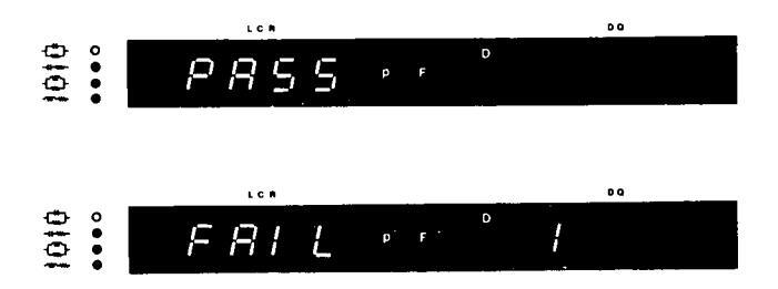
be done under all conditions of FUNCTION and TEST SIGNAL settings. Tests under certain combined conditions of FUNCTION and TEST SIGNAL settings are done for five ranges. A test for a range ends with a display of PASS (normal operation) or FAIL (abnormal operation) and then next range test is started. Range shifting for this test is done automatically from lower to higher.
All the combinations of FUNCTION and TEST SIGNAL switch settings are listed below. Even if the FUNCTION or TEST SIGNAL switch settings are limited for proposed sample measurement, all combined conditions should be tested.
| Pushbutton Switch Setting * |
UNKNOWN**
Connectors |
|---|---|
|
(
C
), (
120Hz
), (
SELF TEST
)***
(C), ( 1 kHz ), ( SELF TEST ) (C), ( 10 kHz ), ( SELF TEST ) |
Open between
HIGH side and Low side |
|
|
|
(
L
), (120 Hz), (
SELF TEST
)
(L), ( 1 kHz ), ( SELF TEST ) (L), ( 10 kHz ), ( SELF TEST ) |
Short between
HIGH side and LOW side. |
|
(
R⁄ESR
), (10 kHz), (
SELF TEST)
(R∕ESR), ( 1 kHz ), ( SELF TEST ) (R∕ESR), ( 120Hz ), ( SELF TEST ) |
* When FUNCTION or TEST SIGNALS switch setting is changed, the SELF TEST switch is automatically disabled. Therefore, whenever a new setting is made, push the SELF TEST switch again.
For ** see page 3-5
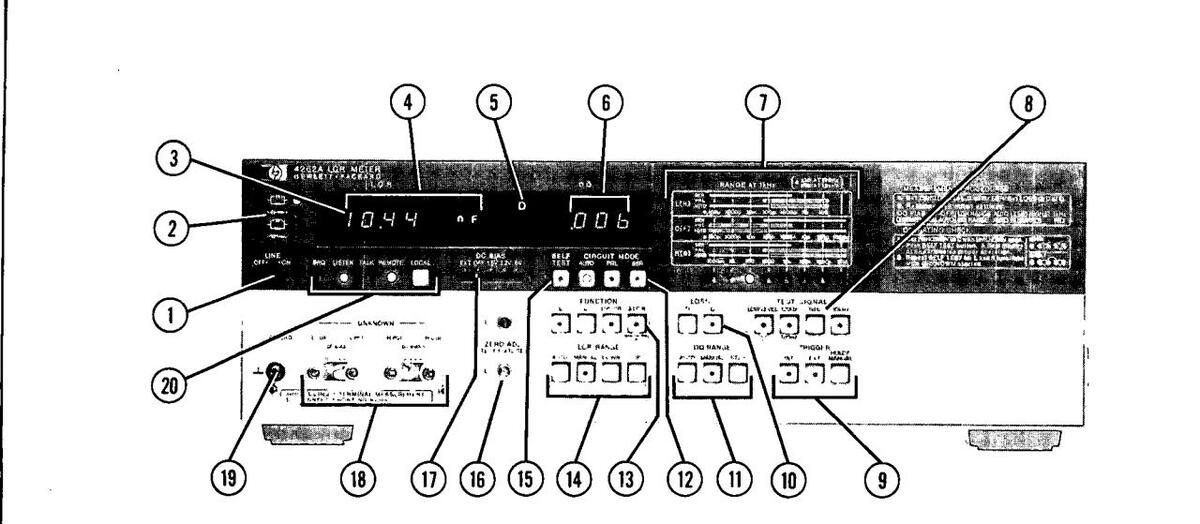
- ① LINE ON/OFF switch: Turns instrument on and readies instrument for measurement
- Circuit Mode Indicator: LED lamp, next to equivalent measuring circuit being used, lights. Sample connected to UNKNOWN terminals (18) is measured in an equivalent circuit selected by FUNCTION (13) and CIRCUIT MODE (12) switches and is indicated by appropriate LED lamp. Equivalent circuits are shown as electronic circuit symbols at the left of indicator lamps. Desired circuit parameter of component is measured in one of the following selected circuit modes:
|
Parallel capacitance
Parallel resistance |
- C |
|---|---|
|
Series capacitance
Series resistance |
|
| Parallel inductance | -[**-] |
|
Series inductance
Series resistance |
-787-444- |
Trigger Lamp: Turns on during sample measuring period. Turns off during period when instrument is not taking measurement (or hold period). There is one turn-on-and-off cycle per measurement. This lamp turns on and off repeatedly when TRIGGER (9) is set to INT.
- LCR Display: Inductance, capacitance or resistance value including the decimal point and unit is displayed in 3-½ digit decimal number from 0000 to 1999. If the sample value exceeds 1999 in a selected range, O-F(Over-Flow) appears in this display. This display also shows PASS or FAIL when SELF TEST is performed.
- D/Q Indicator: In a capacitance or inductance measurement, this indicator indicates which of D (dissipation factor) or Q (quality factor) is displayed in D/Q display 6. In resistance measurement, this indicator is also lit (however, D or Q indication has no meaning and D/Q display 6 is left blank).
- (6) D/Q Display: Value for dissipation factor or quality factor is displayed in capacitance and/or inductance measurement. In resistance measurement, this display is kept blank.
- (1) RANGE Indicator: The range automatically or manually selected is indicated by LED lamp. The table printed above the LED array shows the measurement ranges of the Model 4262A.
- TEST SIGNAL These pushbuttons enable selection of measurement frequency—120Hz, 1kHz or 10kHz and that of low test voltage of the signal applied to sample to be tested. LOW LEVEL switch is effective only in parallel capacitance measurements, supplying a test voltage of 50mVrms. For units equipped with option 010, arrow on pushbutton (120Hz) points to 100Hz.
- IRIGGER: These pushbuttons select trigger mode, INT, EXT or HOLD/MANUAL. INT key provides internal trigger which enables instrument to make repeated automatic measurements. In external trigger mode (EXT), trigger signal should be applied to either of following two connectors: (1) EXT TRIGGER input connector on the rear panel (2) 50 pin connector of Option 001 or 004 on the rear panel. HOLD/MANUAL trigger mode provides trigger signal for one measurement cycle when this key is depressed.
- LOSS: These pushbuttons select whether D or Q value is displayed in the D/Q display (6) in capacitance or inductance measurements.
- D/Q RANGE: These pushbuttons select ranging method for loss measurement. AUTO: Optimum D/Q range is selected by internal logic circuit. MANUAL: D/Q range is fixed to a range. Range change is done by depressing the STEP key on the right.
- (1) CIRCUIT MODE: Appropriate circuit mode for taking a measurement is selected and set with these pushbuttons. A parallel equivalent circuit is selected by PRL key and series equivalent circuit by SER key. When AUTO key is pushed, the instrument automatically selects the appropriate parallel or series equivalent circuit.
-
(13) FUNCTION: These pushbuttons select electrical circuit parameter to be measured as follows:
- C: Capacitance together with dissipation factor (D) or quality factor (Q).
- L:Inductance with dissipation factor (D) or quality factor (Q).
- R/ESR: Resistance or Equivalent Series Resistance.
- △LCR: Difference in L, C, or R value between the value of the sample under test and the internally stored value obtained by a measurement just before △LCR key is depressed.
-
(1) LCR RANGE: These pushbuttons select ranging method for LCR measurement.
- AUTO: Optimum range for the sample value is automatically selected.
- MANUAL: Measurement range is fixed (even when the sample connected to the UNKNOWN terminals is changed). Range change is done by depressing DOWN or UP key on the right.
- (15) SELF TEST: This pushbutton performs automatic check for checking the basic operation of Model 4262A. If normal operation is confirmed, "PASS" is displayed in LCR display ④. If wrong performance is detected, a display of "FAIL" appears. See paragraph 3-5 for details.
- (B) ZERO Adjustment Controls: These adjustments provide proper compensation for cancelling stray capacitance and residual inductance which are present when a test fixture is mounted on the UNKNOWN terminals. Connectors are kept open for cancelling stray capacitance and shorted for cancelling residual inductance.
- 1) DC BIAS Selector Switch: This switch permits selection of internal DC bias voltage applied to sample (1.5Vdc, 2.2Vdc, or 6.0Vdc). When switch is set to EXT, it is used to apply external bias voltage from rear DC BIAS input connectors. OFF position is selected if no bias voltage is necessary.
- (B) UNKNOWN Terminals: Consist of four terminals: High current terminal (Hcure), High potential terminal (HPOT), Low potential terminal (LPOT) and Low current terminal (LCUR). A five-terminal configuration is constructed by adding the GUARD terminal (9). A three-terminal configuration is constructed by shorting High terminals and Low terminals together with shorting bars. Under DC Bias operation, the high terminals have a positive DC voltage with respect to LOW terminals.
- (9) GUARD Terminal: This is connected to chassis ground of instrument and can be used as Guard terminal for increasing accuracy in certain measurements.
- (2) HP-IB Status Indicator and LOCAL switch. LED lamps for SRQ, LISTEN, TALK, and REMOTE which indicate status of interface between the 4262A (Option 101) and HP-IB controller. LOCAL switch enables front panel controls instead of remote control signals from HP-IB line.

** Two HIGH side terminals and two LOW side terminals should be connected with the shorting strap, for each configuration of the UNKNOWN terminals. When the UNKNOWN terminal configuration is not appropriate, for example, shorted (C) or open (L), display will show FAIL 1 (because they result from different causes, FAIL 2 or FAIL 3 are rarely displayed).

*** Setting change required is only the underlined switch setting.
If FAIL is displayed, check the UNKNOWN terminal configurations as follows:
- (1) That the two HIGH side terminals (HCUR HPOT) and the two LOW side terminals (LCUR LPOT) are properly shorted.
- (2) That short or open conditions properly exist between HIGH and LOW side terminals.
- (3) That GUARD terminal is isolated (open) from both of HIGH and LOW terminals.
If FAIL is still displayed (under the above condition), notify the nearest Hewlett-Packard office with information detailing which combination of settings show FAIL.
During SELF TEST, other controls are automatically set as follows:
| CIRCUIT MODE | SER when FUNCTION |
|---|---|
| is set to L or R/ESR. | |
| PRL when FUNCTION | |
| is set to C. | |
| LOSS | D |
| LCR RANGE | |
| D/Q RANGE | MANUAL |
| TRIGGER | INT |
NOTE
TO ENSURE CORRECT RESULTS OF SELF-TEST OPERATION IN L AND R MEASUREMENT FUNCTIONS, CON-NECT ALL (HIGH AND LOW SIDE) UN-KNOWN TERMINALS TOGETHER WITH A LOW IMPEDANCE STRAP (IF THIS SHORT-CIRCUIT IS MADE AT THE ENDS OF THE TEST LEADS, COR-RECT RESULTS MAY NOT OCCUR).
3-7. TEST SIGNALS.
3-8. Three test signal frequencies are available: these are 120Hz, 1kHz and 10kHz sinusoidal waveforms which have a frequency accuracy of 3%. The typical voltage applied to the sample or current flowing through the sample is specified in Table 3-1 for all test signal frequencies. A constant test voltage is supplied to the sample when measuring parallel parameters Lp, Cp, and Rp. The constant current method is adopted for the measurement of Ls, Cs, and Rs. The 50mVrms test voltage is used only for Cp measurement.
3-9. MEASUREMENT RANGE.
3-10. As given in Table 3-2, the 4262A has wide measurement ranges. Seven or eight ranges are available (depending upon measurement function) and the appropriate range is automatically selected for the value of sample connected to the 4262A UNKNOWN terminals. For applications which require a fixed measurement range (such applications are sometimes needed for example in inductance measurements) manual range control is pushbutton selectable. Four or five ranges, however, are used in the series and parallel equivalent circuit measurement modes. When the CIRCUIT MODE is set to AUTO, the 4262A will automatically select the appropriate circuit mode, range over the measurement ranges shadowed in Table 3-2, settle on the proper range, and measure the sample.
Table 3-1. Sample Voltage or Current.
| PANCE | CIRCUIT | MODE | ||||
|---|---|---|---|---|---|---|
| RANGE | Ls | Lp | Cs | Ср | Rs | Rp |
| 1 | 40mA rms | 1Vrms(50mVrms)* | 40mA rms | |||
| 2 | 10mA rms | _ | 1Vrms (50mVrms)* | 10mA rms | ||
| 3 | 1mA rms | 1Vrms(50mVrms)* | 1mA rms | |||
| 4 | 100 µA rms | 1V rms | 10 µA rms | lVrms (50mVrms)* | 100 µA rms | 1V rms |
| 5 | 10 µA rms | 1V rms | 100 µA rms | 1Vrms (50mVrms)* | 10 µA rms | 1V rms |
| 6 | 1V rms | 1 μA rms | 1V rms | |||
| 7 | 1V rms | 10mA rms | 1V rms | |||
| 8 | 40mArms | 1V rms |
*When TEST SIGNAL is set to LOW LEVEL.
| CIRCUIT | TEST | Ra | inge | ||||||
|---|---|---|---|---|---|---|---|---|---|
| MODE | Frequency | 1 | 2 | 3 | 4 | 5 | 6 | 7 | 8 |
| Lp |
120 Hz
1 kHz 10 kHz |
0000 mH
000.0 mH 00.00 mH |
00,00 H
0000 mH Hm 0,000 |
000.0 H
00.00 H 0000mH |
0000 H
000.0 H 00.00 H |
||||
| Ls |
120 Hz
1 kHz 10 kHz |
14 0000
Hμ 0.000 Hμ 00.00 |
00,00 mH
0000 μH 000,0 μH |
000,0mH
00,00mH 0000 μH |
0000 mH
000.0 mH 00.00 mH |
00.00 H
0000 mH 000.0 mH |
|||
| Ср |
120 Hz
1 kHz 10 kHz |
0000 pF
000.0 pF 00.00 pF |
00.00 nF
0000 pF 000.0 pF |
000.0 nF
00.00 nF 0000 pF |
0000 nF
000.0 nF 00.00 nF |
00.00 μF
0000 nF 000.0 nF |
|||
| Cs |
120 Hz
1 kHz 10 kHz |
0000 nF
000.0 nF 00.00 nF |
00.00 μF
0000 nF 000.0 nF |
000.0μF
00.00μF 0000 nF |
0000 μF
000.0 μF 00.00 μF |
00,00mF
0000 μF 000.0 μF |
|||
| Rp |
120 Hz
1 kHz 10 kHz |
Ω 0000
Ω 0000 Ω 0000 |
00.00 kΩ
00.00 kΩ 00.00 kΩ |
000.0 kΩ
000.0 kΩ 000.0 kΩ |
0000 kΩ
0000 kΩ 0000 kΩ |
00,00 ΜΩ
00,00 ΜΩ 00,00 ΜΩ |
|||
| Rs |
120 Hz
1 kHz 10 kHz |
Ωm 0000
Ωm 0000 Ωm 0000 |
Ω 00.00
Ω 00.00 Ω 00.00 |
000.0Ω
000.0Ω 000.0Ω |
Ω 0000
Ω 0000 Ω 0000 |
00.00 kΩ
00.00 kΩ 00.00 kΩ |
|||
| Note: 0 | 0000µH inc | licates a ra | inge of 000 | )1µH to 19 | 99µH ( an | d similarly | for F and | Ω). |
Table 3-2. Measurement Ranges.
Model 4262A
3-11. INITIAL DISPLAY TEST.
3-12. The Model 4262A automatically performs a front panel LED display test for a few seconds after instrument is tuned on (after LINE button is depressed). The display test sequence is:
- 1. All front panel indicator lamps, except numeric segments and multiplier indicator lamps will illuminate. (SRQ, LISTEN, TALK and REMOTE lamps illuminate only when HP-IB option is installed).
- 2. Front panel pushbutton LED's and indicator lamps indicate that automatic initial settings (see Paragraph 3-13 which follows) have been set. Simultaneously, the LCR DISPLAY and DQ DISPLAY readouts are tested. All numeric displays show figures of 8 ( ) and multiplier indicators (p n μ m k M) light in turn.
- 3. Range indicator lamps step from right (upper range) to left (lower range). When steps 1, 2 and 3 have been completed, the trigger lamp begins to flash. Figures on numeric displays change to meaningful numbers showing that the 4262A is ready to take a measurement.
3-13. INITIAL CONTROL SETTINGS.
3-14. One of the sophisticated features of the 4262A is its automatic initial control setting function. After the instrument is turned on, the front panel control functions are automatically set as follows:
| SELF TESTOFF | |
|---|---|
| CIRCUIT MODE AUTO | |
| FUNCTIONC | |
| LCR RANGE AUTO | |
| LOSS D | |
| DQ RANGE AUTO | |
| TEST SIGNAL 1kHz | |
| TRIGGER INT |
As these initial settings provide the general capacitance measurement conditions applicable to a broad range of capacitance measurements, a capacitance can be usually measured by merely connecting the sample to the UNKNOWN terminals. Inductance or resistance can be measured by pressing the L FUNCTION or R/ESR FUNCTION buttons, as appropriate. When a different measurement is to be attempted, press appropriate pushbuttons and select desired functions.
3-15. D/Q MEASUREMENT.
3-16. The Model 4262A makes a loss measurement along with capacitance or inductance measurements on each measurement cycle. The measured loss factor is displayed in the form of the dissipation (D) or quality (Q) factor of the sample. The D or Q function is pushbutton selectable in both L and C measurements. D and Q measurement ranges are:
| D: | 2 ranges | .001 to 1.999 |
|---|---|---|
| - | 0.01 to 19.9 | |
| Q: | 4 ranges | .050 to 1.996 |
| 0.05 to 19.61 | ||
| .00.1 to 166.7 | ||
| 001 to 1000 |
The D range, appropriate to the value of the sample is automatically selected. Alternately, a manual D range control is pushbutton selectable. Quality factor (Q) is calculated as a reciprocal dissipation number from the measured D value. Hence, the Q readout display will skip some numbers when low dissipation samples are measured. For example, when the dissipation measured is .010, the quality factor display is 100. When dissipation is .009, the quality factor reading is 111 (Q readings of 101 to 110 are not obtained). On the high D measurement range, the readout is displayed in 3 digits.
3-17. △ LCR MEASUREMENT.
3-18. When many components of similar value are to be tested, it is sometimes more practicable to measure the difference between the value of the sample and a predetermined reference value. The △LCR function permits repetitive calculation of the difference between the reference and each individual sample and to display the result on the LCR DISPLAY. When the ALCR FUNCTION button is pressed, the inductance, capacitance, or resistance value of the sample is stored in an internal memory. The 4262A will now display the difference between the stored value and the measured value of a sample connected to UNKNOWN. The LCR RANGE is automatically held in MANUAL for the duration of ALCR measurements (if another pushbutton is inadvertently pressed, the ALCR measurement function will be reset and will require reactivating).
| Section | ш |
|---|---|
| Figure | 3-3 |
| Accessory Model | Characteristics | ||||||||||
|---|---|---|---|---|---|---|---|---|---|---|---|
| 16061A Test Fixture |
This fixture facilitates easy measurement of general
type components with axial or vertical leads. To install fixture, disconnect shorting bars between high terminals and between low terminals. Insert fix- ture screws to firmly attach fixture to instrument. Two kinds of inserts are included (for components with either axial or vertical leads). |
l
n fix- |
|||||||||
| D | UT ra |
inge (a
F |
at 1k |
Hz)
n |
F | μF | |||||
| e entre |
μ
S |
H
2 1 |
0 1 |
m
00 k |
Η
Ω + |
10 1 | 00 N |
Η
/Ω |
10 1 | .00 | |
| 1 | С | ||||||||||
| Five terminal construction test fixture. |
L
R |
||||||||||
| 16062A Test Leads | T |
|
he 16 |
|
062A |
is esp |
pecial |
|
ly use |
|
ful wl |
hen m | neasu |
ring le |
bw |
|
in
ar m 10 po |
npeda
e diag ore th 00µH otenti leasur |
nces.
gramm aan ap at 1 k al lead able E bF |
DUI
ped b prox Hz, if ds and DUT 1 |
value
elow. . 300/ ; is red d curr canges n m |
es me
If th uF at comm ent le (at 1 uF |
asurai
e mea 1kHz endec ads b kHz) |
ble wi
isurin or le d that e twis |
uth the same set of the set of th |
ae 160
nple is an app respec cogeth |
orox.
etive er. |
|
| _ | Ω 1 | 0 1 | 00 k |
Ω :
| |
00 N |
/Ω
| |
10 1 | 00 | |||
| Test Leads for four terminal measurement (does not contain guard conductor). |
L
R |
||||||||||
| 16063A Test Leads The 16063A is particularly useful when measuring impedances. DUT values measurable with the 16 are diagrammed below. This test lead set is not in tended to be used for the accurate measurement small capacitances (less than approx. 100pF) due the residual capacitance of the leads. Measurable DUT ranges (at 1kHz) pF nF μF U mH H |
suring
le 160 not in- nent o due t |
high
63A f :0 |
|||||||||
| c |
μ
S |
1 1 | 0 1 | .0 1( | 10 1 | 00 | |||||
| Coaxial test leads with guard conductor | L | - | - | + | |||||||
| for three terminal measurement. | R | ╞ | |||||||||
Figure 3-3. Test Fixture and Leads.
3-19. D/Q Blanking Function (Switch selectable function inside cabinet).
3-20. The D/Q blanking function permits deactivating the D/Q measurement as desired. If operator has no need of D/Q measurement data, and alternatively desires to make higher speed LCR measurements, the switch for this function may be set. When the D/Q function is deactivated, measurement time is shortened to approximately 220 to 250 milliseconds (at 120Hz) and to 80 to 110 milliseconds (at 1kHz and 10kHz) as compared to standard measuring times (which includes a D/Q measurement). The D/Q deactivating switch is located on the A23 board assembly. To select this function, change setting of the switch as follows:
- a. Remove top cover.
- b. Take out A23 board (red and orange colored extractors).
- c. The selection switch is mounted near left edge of the A23 board.
- d. Change position of the switch as illustrated below.
- e. Reinstall the A23 board in its normal position,
f. Replace top cover.
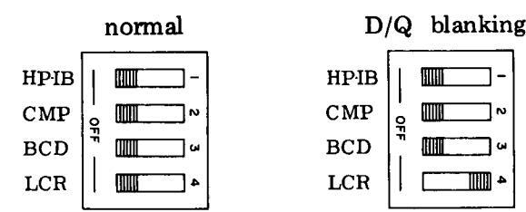
3-21, General Component Measurement.
3-22. Figure 3-7 shows the operating procedures for measuring an L, C or R (inductance, capacitance or resistance) circuit component. Almost all discrete circuit components (inductors, capacitors or resistors) except for components having special shapes or dimensions can be measured with this setup. Special components may be measured by using Test Leads 16062A or 16063A or by specially designed user built fixtures instead of 16061A Test Fixture.
3-23. Semiconductor Device Measurement.
3-24. The procedures for using the 4262A semiconductor device measurement capabilities are described in Figure 3-8. For example, the junction (interterminal) capacitance of diodes, collector output capacitance of transistors, etc., can easily and accurately be measured (with and without dc bias).
3-25. External DC Bias.
3-26. A special biasing circuit using external voltage or current bias, as needed for capacitor or inductor measurements, is illustrated in Figure 3-9. The figure shows sample circuitry appropriate to 4262A applications. Biasing circuits must avoid permitting dc current to flow into the 4262A as dc current increases the measurement error and the excess current sometimes may cause damage to the instrument. When applying a dc voltage to capacitors, be sure applied voltage does not exceed maximum working voltage and that you are observing polarity of capacitor. Note that the external bias voltage is present at HCUR and HFOT terminals.
3-27. Bias Voltage Settling Time. When a measurement with dc bias voltage superposed is performed, it takes some time for voltage across sample to reach a certain percentage of applied (desired) voltage. Figure 3-9 shows time for dc bias voltage to reach more than 99% of applied voltage and for 4262A to display a stable value. If the bias voltage across sample is not given sufficient time to settle, the displayed value may fluctuate or O-F may be displayed. Read measured value after display settles.
3-28. External Triggering.
3-29. For triggering the 4262A externally, connect an external triggering device to the rear panel EXT TRIGGER connector (BNC type) and press EXT TRIGGER button. The 4262A can be triggered by a TTL level signal that changes from low (0V) to high level (+5V). Triggering can be also done by alternately shorting and opening the center conductor of the EXT TRIGGER connector to ground (chassis).
Note
The center conductor of the EXT TRIGGER connector is normally at high level (no input).
3-30. TERMINAL CONFIGURATION.
3-31. Connection of DUT. The 4262A Unknown terminals consists of five binding post (type) connectors: HCUR, HPOT, LCUR, LPOT and GUARD. By connecting the stationary shorting straps to appropriate terminals, the UNKNOWN terminals can be adopted for the desired measurement terminal configuration: the two, three, four or five terminal method.
For measurements of samples having a medium order of impedance (100 Ω to 10kΩ), the convenient two terminal method is suited to measurement requirements for good accuracy as well as for ease in connecting the sample. When converting to two terminals, shorting straps are attached to the UNKNOWN HCUR and HPOT terminals, and LCUR and LPOT terminals, respectively.
High impedance samples (greater than 1kΩ) -which includes low capacitance, high inductance and high resistance -- should be measured by the three terminal method to eliminate the effects of stray capacitances on the measurements. For this purpose, the guard conductor of the sample is connected to the instrument GUARD terminal.
In the measurement of low impedance samples (less than 1kΩ), efforts should be made to eliminate the effects of contact resistance. lead resistance, residual inductance and other residual parameters in the measuring apparatus. Four terminal configuration measurements allow stable. accurate measurement of high capacitance. low inductance and low resistance samples at minimum incremental errors in the measurement of low impedance samples. In the four terminal method, the shorting straps are disconnected to separate potential leads from current leads. Thereby, the characteristics of the sample can be precisely determined by the instrument irrespective of the various residual parameters present in the measuring signal current path. To ensure the best accuracy, the potential leads should be connected near to the sample.
The five terminal method, which adds the guard conductor to the four terminal configuration, expands the applicable measurement range into the higher impedance regions. Thus, this method covers a broad range of measurements from low to high impedance samples at the measuring frequency of the 4262A.
When test fixtures and test leads used have a shielding conductor and are designed to consider residual impedance, the measurement limitations described above for the individual terminal configurations can vary to some extent depending on the particular characteristics of the fixture and connections. Three accessories, the 16061A Test Fixture, the 16062A Test Leads, and the 16063A Test Leads are available. The characteristics of these accessories and applicable measurement ranges are outlined in Figure 3-3. These accessories make it easy to construct the desired terminal configuration.
FOR CERTAIN TERMINAL MEAS-UREMENT CONFIGURATIONS, THE HCUR TERMINAL MUST BE CON-NECTED TO HPOT TERMINAL AND THE LCUR TERMINAL CONNECTED TO THE LPOT TERMINAL. OTHER-WISE, THE DISPLAYS WILL HAVE NO MEANING AND THE LIFE OF THE RELAYS USED IN THE INSTRU-MENT WILL SOMETIMES BE SHORT-ENED.
Note
The 4262A can not measure a sample which has one lead connected to earth (grounded).
3-32. OFFSET ADJUSTMENT.
3-33 Since test fixtures and test leads have different inherent stray capacitances and residual inductances, the measured value obtained with respect to the same sample may possibly differ depending on the test fixture (leads) used. These residual factors can be read from the 4262A display by properly terminating (short or open) the measurement terminals of the test jig. The front panel C ZERO ADJ and L ZERO ADJ controls permit compensation for these residual factors and can eliminate measurement errors due to the test jig. The capacitance or inductance readout can be set to zero for the particular test jig used with the instrument. In capacitance and inductance measurements, an incomplete offset adjustment causes two types errors:
1) Deviation from zero counts.
When a small capacity or a small inductance is measured, the measured capacitance (inductance) value becomes the sum of the capacitance (inductance) of sample and the stray capacitance (residual inductance) of test jig. The effects of the residual factors are:
Cm = Cx + Cst Lm = Lx + Lres
Where, subscripts are
| m: | measured value. |
|---|---|
| malue of comple |
- x: value of sample. st: stray capacitance.
- res: residual inductance.
Both Cst and Lres cause the same measurement error and are independent of sample value.
2) Influence on high capacitance and high inductance measurements.
When a high inductance (a high capacitance) is measured, the residual factors in the test jig also contribute a measurement error. The affect of stray capacitance or residual inductance on measurement parameters are:
| Stray capacitance | → Offsets high inductance measurements. |
|---|---|
| Residual inductanc |
e → Offsets high capacitance
measurements. |
These measurement errors increase in proportional to the square of the test signal frequency. The effects of the residual factors can be expressed as follows:
or
or
In a 10kHz measurement, for the measurement error to be less than 0.1%, the product of Cx and Lres (Lx and Cst) should be less than 0.25 x 10⁻¹². The relationship between the residual factors of the test jig and measurement accuracies are graphically shown in Figure 3-4.
The 4262A ZERO ADJ controls cover the following capacitance and inductance offset adjustment ranges:
C ZERO ADJ: up to L ZERO ADJ: up to H
An offset adjustment should always be performed before measurements are taken.
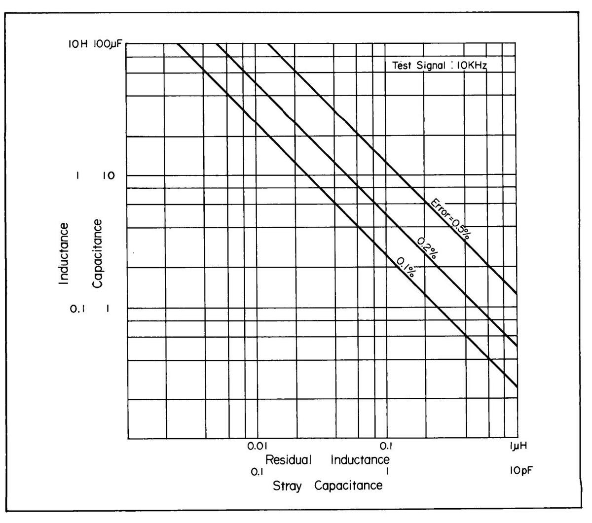
Figure 3-4. Measurement Error due to Misadjusted ZERO ADJ Controls.
Measurement Parameter Conversions
Parameter values for a component measured in a parallel equivalent circuit and that measured in series equivalent circuit are different from each other. For example, the parallel capacitance of a given component is not equal to the series capacitance of that component Figure A shows the relationshing hetween narallel and series narameters for various values of D. Applicable diagrams and equations are given in the chart. For example, a parallel capacitance (Cp) of 1000pF with a dissipation factor of 0.5, is equivalent to a series capacitance (Cs) value of 1250pF at 1kHz. As shown in Figure A inductance or capacitance values for parallel and series equivalents are almost identical when the dissipation factor is less than 0.01. The letter D in Figure A represents dissipation factor and is calculated by the equations presented in Table A for each circuit mode. The dissipation factor of a component always has the same dissipation factor at
a given frequency for both parallel equivalent and series equivalent circuits.
Note
Dissipation factors displayed when CIRCUIT MODE is switched between PRL and SER may exhibit slight differences due to the measurement accuracy of the 4262A.
The reciprocal of the dissipation factor (D) is quality factor (Q) and D is often represented as tan δ which is the tangent of the dissipation angle (δ). Figure 3-6 is a graphical presentation of the equations in Table A. For example, a series inductance of 1000µH which has a dissipation factor of 0.5 at 1kHz has a series resistance of 3.14 ohms.
Table A. Dissipation Factor Equations.
| Circuit Mode | Dissipation Factor | Conversion to other modes | |
|---|---|---|---|
| Cp mode | D = 1/(2 \pi fCpRp) (= 1/Q) |
Cs = (1 + D
2
)Cp, Rs =
D
2
1 + D 2 · Rp |
|
| Cs mode | Cs Rs | D = 2πfCsRs (= 1/Q) | Cp = 1/(1+D 2 ) Cs, Rp = 1/(D 2 ) Rs |
| Lp mode | D = \frac{2\pi fLp}{Rp} \left(= \frac{1}{Q}\right) |
Ls =
1
1 + D 2 Lp, Rs = D 2 1 + D 2 · Rp |
|
| Ls mode | -787-444- | D = Rs/2 fLs (= 1/Q) | Lp = (1 + D 2 )Ls, Rp ≈ 1 + D 2 /D 2 · Rs |
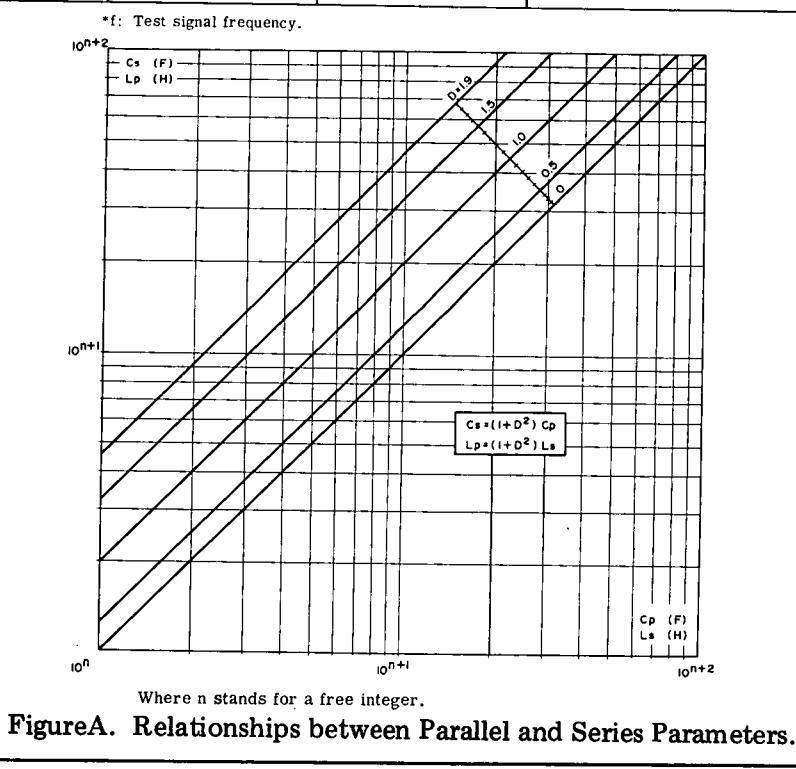


Model 4262A
Section III Figure 3-5
Figure 3-6. Relationship of Dissipation to Series and Parallel Resistance.
Table 3-3. Annunciation Display Meanings.
| LCR DISPLAY DQ | Indicated Condition | Action |
|
FUNCTION has been inappro-
priately set. |
Change 4262A FUNCTION to
L, C or R suitable for the sample being measured. |
|
|
Measured L or C value exceeds
1999 counts. DQ display indicates that DQ measurement has been omitted. |
Set 4262A to:
CIRCUIT MODE: AUTO LCR RANGE: AUTO |
|
| Measured R value exceeds 1999 counts. | Try changing TEST SIGNAL to 120, 1k or 10kHz. | |
| I.2.3 III IIII (any LCR (overflowed) reading) |
Measured D/Q value exceeds the
upper range limit (1999 counts). Accuracy of LCR readings may not be within specifications. |
Set 4262A DQ RANGE to
AUTO. Try changing TEST SIGNAL to 120, 1k or 10kHz. |
| LI – E L |
CIRCUIT MODE setting is not
suitable for the sample being measured. |
Set 4262A to:
CIRCUIT MODE: AUTO |
|
Measured L, C or R value is ex-
tremely large or small compared with the selected range. |
Try changing TEST SIGNAL
to 120, 1k or 10kHz. |
|
| 18 1 |
When Measured L or C value is less
than 80 counts, DQ measurement is omitted. |
Set 4262A LCR RANGE to
AUTO. Try changing TEST SIGNAL to 120, 1k or 10kHz. |
|
(any DQ
reading) |
In △LCR measurement, the differ-
ence between the preset value and the measured value of the sample exceeds -999 counts. |
|
|
In △LCR measurement, the cal-
culated difference exceeds -999 counts. In addition, the value of measured sample is less than 80 counts. |
||
| Minus (-) is displayed. |
Minus display sometimes occurs
when sample having a value around zero is measured. |
Zero count display is meaning-
ful when minus (-) display repeatedly turns on and off. |
|
Sometimes a minus display occurs
when a capacitor (or inductor) is measured in L (or C) FUNCTION. |
Change to appropriate
FUNCTION. |
|
| Offset adjustment signal applied is too great (causes minus display). | Readjust offset signal for proper magnitude. |

7. Rotate L ZERO ADJ control until inductance readout is 000 counts on LCR DISPLAY.
Note
To achieve more critical zero adjustments, when 10kHz test signal frequency is used, perform the capacitance and inductance zero offset adjustments (steps 4, 5, 6 and 7) at 10kHz.
- 8. Remove shorting lead from 16061A.
- 9. Select desired FUNCTION, either L, C or R/ESR.
- 10. Connect sample to be measured (L, C or R) to Test Fixture.
- 11. Model 4262A will automatically display value of unknown.
Note
If O-F, U-CL, minus (-) or blank display occurs, see Table 3-3 for solution. Measured values for semiconductor devices are sometimes unreliable when TEST SIGNAL LOW LEVEL pushbutton is in its normal (1V) state (button lamp is not lit). In these instances, follow Figure 3-8 for semiconductor device measurement.
Note
If manual triggering is required, press HOLD/ MANUAL button. Each time the button is pressed, the instrument is triggered.
12. If internal DC bias is required, set DC BIAS switch to 1.5V, 2.2V or 6V: If not, OFF position should be selected.
Note
DC bias application may only be used for capacitance measurements.
CAUTION
POSITIVE POLE OF ELECTROLYTIC CAPA-CITOR MUST BE CONNECTED TO HIGH TERMINALS AS PLUS BIAS VOLTAGE IS APPLIED TO HIGH TERMINALS WITH RE-SPECT TO LOW TERMINALS.
Note
An external bias voltage up to +40V may be applied to EXT DC BIAS rear panel connector. Connect DC power supply to EXT DC BIAS connector. Set DC BIAS switch to EXT.
CAUTION
EXTERNAL DC BIAS AT EXT BIAS CON-NECTOR MUST NEVER EXCEED +40V.
13. Read measured value on display.
Note
It is usually recommended that the LCR RANGE be set to MANUAL and to hold the range when measuring multiple samples having almost the same value. Range hold operation will somewhat shorten measurement time.
Note
Series resistance of electrolytic capacitors, inductors or transformers can be measured in series R/ESR measurement mode. In these cases, the number of digits is sometimes reduced. On the other hand, resistance can, of course, be indirectly measured with the C/L FUNCTION and calculated from one of the following equations:
Rs = D/ωCs (Cs-D measurement) Rs = ωLs · D (Ls-D measurement) Rs = ωLp · D (Lp-D measurement)
The above relationships are graphically shown in Figure 3-6.
DO NOT CONNECT A CHARGED CAPACITOR (EXCEEDING 40V) DIRECTLY TO THE UNKNOWN TERMINALS AS A DUT.
_____ CAUTION _____
— CAUTION —
NEVER APPLY A DC VOLTAGE DIRECTLY BETWEEN THE UNKNOWN H AND L TERMINALS WITHOUT PROPER PROTECTION AGAINST A POSSIBLE HARMFUL CURRENT. DC VOLTAGE MUST NOT BE APPLIED TO THE L TERMINAL WITH RESPECT TO GROUND.
Figure 3-7. General Component Measurements (Sheet 3 of 3).
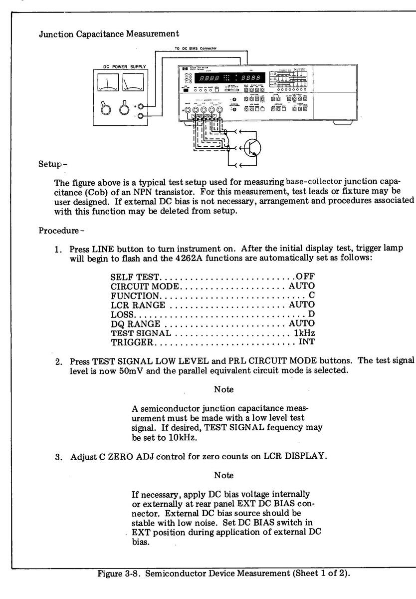

Figure 3-8. Semiconductor Device Measurement (Sheet 2 of 2).

Note
+E voltage is applied to Cx in figure. -E voltage can be applied to Cx in this figure. In the above arrangement, the polarity of Cx and C1 must be taken into consideration.
CATUION
NEVER SHORT BETWEEN HPOT AND LOW TERMINALS WHEN R1 IS SMALLER THAN 1kΩ. MAKE SURE THAT UNKNOWN CAPA-CITOR IS NOT DEFECTIVE BEFORE CON-NECTING TO INSTURMENT.
TO AVOID HARMFUL SURGE CURRENT WHICH MAY FLOW THROUGH INTERNAL CIRCUITRY WHEN A HIGH VOLTAGE DC BIAS IS SUDDENLY APPLIED, IT IS RECOM-MENDED THAT DC BIAS BE GRADUALLY INCREASED FROM A LOWER VOLTAGE.
Note
Ripple or noise of external dc bias source should be as low as possible. The low frequency noise of bias source should be less than 1mVrms for a TEST SIGNAL level of 50mV (LOW LEVEL) and 30mVrms for 1V.
Figure 3-9. External DC Bias Circuit (Sheet 1 of 3).
2. Minimum values for both C1 (dc blocking capacitor) and R1 are given in table below:
Note
Insulation resistance for Cx must be greater than a certain minimum value. Refer to Table 3-4 for unusual operating indications.
|
Range
(at 120Hz) |
1000pF | 10.00nF | 100.0nF | 1000nF | 10.00µF |
|---|---|---|---|---|---|
|
Minimum
C1 |
0.01µF | 0.1µF | 1µF | 10µF | 10.00µF |
|
Minimum
R1 |
300kΩ | 100k Ω | 10k Ω | 1kΩ | 100Ω |
In 1kHz(10kHz) measurement, multiply both range value and value of C1 by 1/10 (1/100). If the calculated value of C1 is less than 0.01µF, use 0.01µF capacitor.
Note
DC withstand voltage for C1 capacitor must be greater than dc applied voltage E. Also observe polarity of capacitor C1 with respect to applied voltage.
3. Set 4262A controls as follows:
| SELF TEST | |
|---|---|
| FUNCTION | |
| CIRCUIT MODE PRL | |
| Other controlsany setting |
4. Read displayed value after allowing time for bias voltage to settle. Typical settling times are:

Figure 3-9. External DC Bias Circuit (Sheet 2 of 3).

Figure 3-9. External DC Bias Circuit (Sheet 3 of 3).
|
A and/or B may occur in the following
Resistance of low loss inductor or capacitor being measured in R FUNO Inductance of lossy inductor or capac of lossy capacitor being measured C FUNCTION. |
| What to do: | |
|
A. Do not set CIRCUIT MODE to AUTO
Set CIRCUIT MODE to a PRL or SEL setting that shows a valid display. |
|
|
B. Set LCR RANGE to MANUAL.
Manually settle the instrument on an appropriate range. |
|
| Indication: | Cause of trouble: |
|
The displayed value fluctuates on minin
capacitance, maximum inductance or maximum resistance ranges in either J |
Here are some of the reasons why thin happens: |
| or SER circuit modes. |
|
|
exists near the 4262A.
C. The 4262A and sample are connectogether with relatively long, non-shielded cable. |
|
| What to do: | |
|
GUARD LCUR LPOT H POT H CUR
DC BIAS - DC BIAS + |
|
|
2. Use shielded cable for connection
between sample and the instrumer Connect cable shield to GUARD. |
|
| Metal Case | |
Table 3-4. Unusual Operating Indications (Sheet 1 of 4).
Table 3-4. Unusual Operating Indications (Sheet 2 of 4).
| ······································ | |||
|---|---|---|---|
|
When measuring a low impedance (small
inductance, resistance or high capacitance), measurement error is excessive. |
|
sidual impedance(inductance)
r resistance) of test leads ninal measurement. ad induction between (H CUR and L CUR ) and s (H POT and L POT ). |
|
| What to do: | |||
|
Use test leads in
figuration and me Twist current lea Do the same with L POT ). |
four-terminal con-
asure. ds (H CUR and L CUR ) together. potential leads (H POT and |
||
|
Additional error is presented as
$\omega^2_LrCx X 100 (%)$ for C measurement, where: $\omega = 2\pi f$ f = test frequency Lr = residual inductance Cx = unknown capacitance |
|||
| adication: | Cause of trouble: | ||
| Maggungen ont owner is everyosize when high | Measurement | Cause of error | |
| impedance (high inductance, small capacitance) is measured. | High Inductance |
Stray capacitance
between High and Low leads. |
|
|
Small
Capacitance |
Stray capacitance
between High and Low leads. |
||
|
1
- |
What to do: | ||
|
Use shielded cab
between sample a terminals. Co to GUARD termin |
le for connection
und 4262A UNKNOWN nnect outer conductor aal. |
||
| Adjust C ZERO A compensate for s | ADJ control properly to tray capacitance. | ||
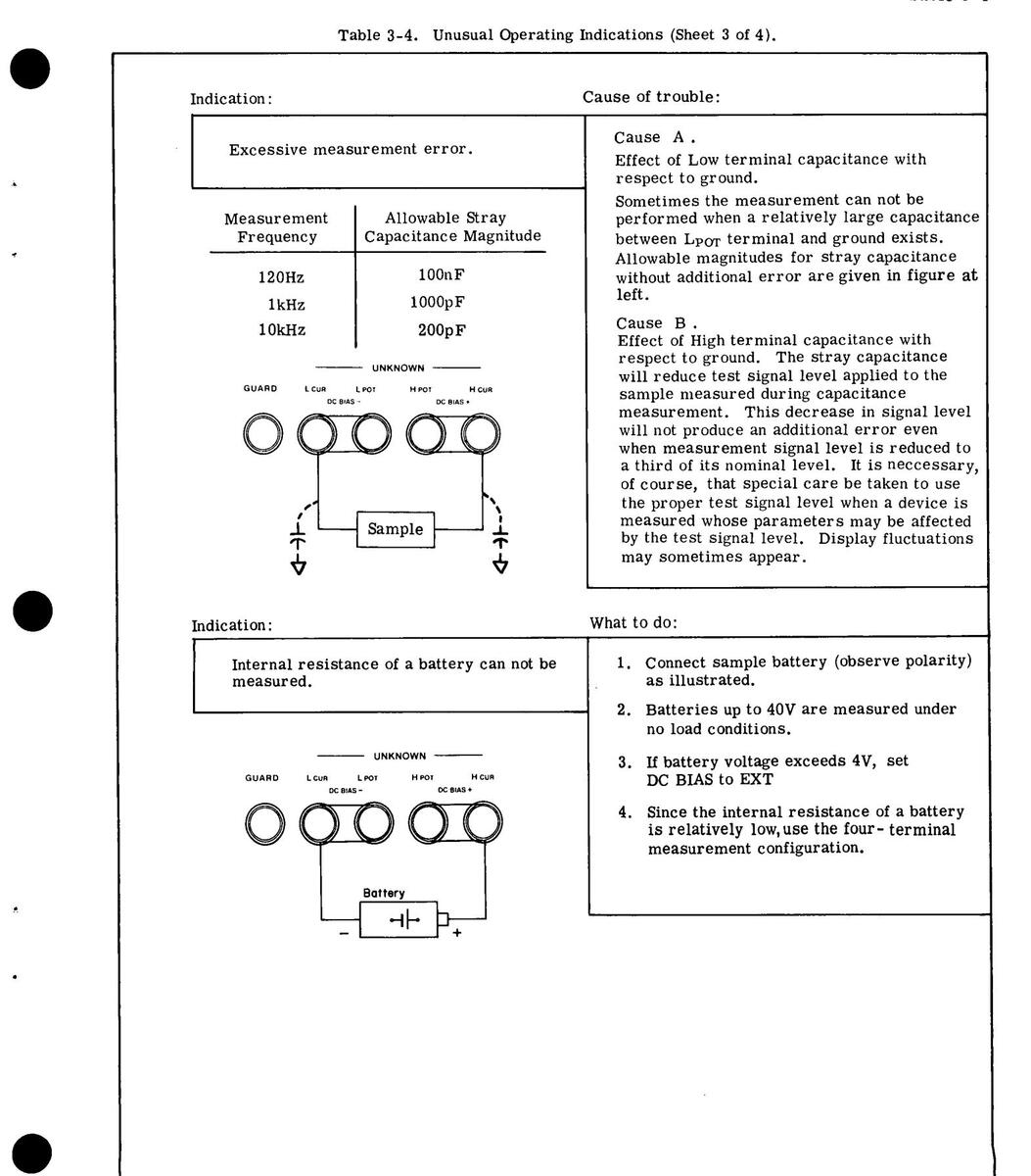
3-25
Table 3-4. Unusual Operating Indications (Sheet 4 of 4).
| when a samplinductor) is m | e (for e: | vamnle an i | When a sample (for example, on inch core | ||||||
|---|---|---|---|---|---|---|---|---|---|
|
When a sample (for example, an iron core
inductor) is measured in AUTO of CIRCUIT MODE, the instrument repeats range selection and does not complete the meas- urement depending upon level of test current used. |
The measurement reading of sample
depends on the level of measurement test signal applied. |
||||||||
| What to do: | |||||||||
|
Set LCR
Manually an approp |
RANGE to M
settle the in priate range. |
ANUAL.
strument on |
|||||||
| ation : | |||||||||
| When a capacitor is measured with dc bias voltage applied, an abnormal display occurs. |
There are
insulatior measured |
e limitations
n resistance l with dc bias |
to the permi
of a capacito 5. See table |
ssible
r below. |
|||||
| MODE | RANGE | ||||||||
| 1kHz | Ср | 100.0pF | 1000pF | 10.00nF | 100.0nF | 1000nF | |||
| 100 0 5 | 1000 1 | 10.00.00 | 100 0.10 | 1000 - | |||||
Note
In 120Hz(10kHz) measurement, multiply range value by 10(1/10).
Ri given in above table is applicable for a dc bias of 40 V. When the bias voltage is less than 40 V, Ri limit is RiVb/40 (Ω) where Ri is value given in the table and Vb is applied dc bias voltage.
3-40. OPTION OPERATION.
3-41. Operating instructions for Options 001, 004, and 101 are described in the following paragraphs.
3-42. OPTION 001: BCD PARALLEL DATA OUTPUT.
3-42. The 4262A Option 001 provides parallel BCD outputs for LCR display, D/Q display and information for various control settings. These outputs are fed to two 50 pin connectors on the rear panel.
3-44. Output Data and Pin Assignment.
3-45. The 4262A Option 001 provides eight kinds of output data:
- (1) FUNCTION and CIRCUIT MODE.
- (2) Test Signal Frequency (LOW LEVEL or normal is excluded).
- (3) Annunciator: Normal, Overflow, Uncal, (LCR and D/Q are not annunciated).
- (4) Unit: p, n, μ, m, k, M, D, Q (judgement whether capacitance, inductance or resistance depends on output of FUNCTION switch setting information).
- (5) Decimal Point.
- (6) Polarity.
- (7) Displayed value.
- (8) Other Input/Output Signals.
The signal pin assignments for the 50 pin connector are shown in Figure 3-40. When these signals are fed to digital printer, the print-out is given as a 10 digit decimal number.
3-46. Alternate Output of LCR and D/Q Data.
BCD outputs for LCR and D/Q data of 4262A Option 001 can be alternately supplied through one 50 pin BCD LCR DATA OUTPUT connector on rear panel. This alternate output is enabled by changing slide switch setting on printed circuit board P/N 04262-66535. PC board 04262-66535 is located nearest to the rear panel in the right hand row of PC boards. Normal setting of the four section slide switch for parallel output and the setting for alternate output are illustrated below.
Normal Parallel output:
- Alt

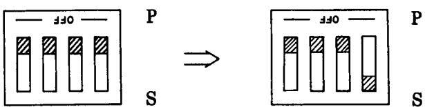
3-47. Output Timing.
3-48. Timing charts for parallel (simultaneous) output and alternate output are shown in Figure 3-41.
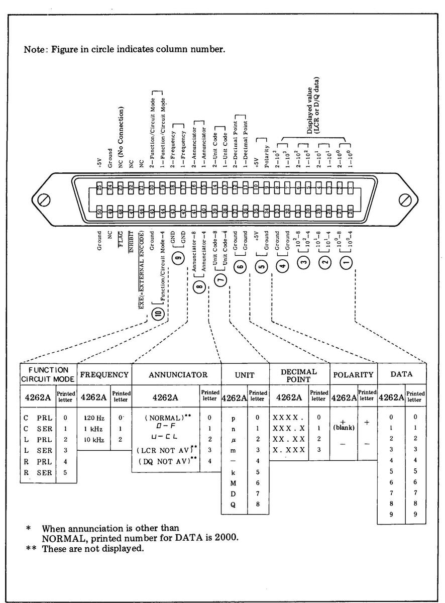
Figure 3-40. Pin Assignments of Output Connector and Output Format.

3-49. OPTION 004- COMPARATOR.
3-50. The 4262A Option 004 (shown in Figure 3-43) provides:
- (a) HIGH and LOW limits setting for comparison of LCR and D/Q measured data.
- (b) LED visual decision output lamps display of results of HIGH and LOW limit comparisons.
- (c) TTL outputs and relay outputs for HIGH, IN, and LOW decision outputs.
-
3-51. Front Panel Features (Figure 3-42).
- (1) LCR LIMIT Switch: Two four-digit switches provide HIGH and LOW limit values with which measured LCR value is compared. Setting range is from 0000 to 1999.
- (2) LCR Decision Output Lamp: Results of comparison are indicated by LED lamps as follows:
HIGH: (measured value ≥ High limit) IN: (Low limit ≤ measured value < High limit) LOW: (measured value ≤ Low limit)
(3) LCR LIMIT CHECK Switch: While this switch is depressed, HIGH and LOW limit values set by LCR LIMIT switches (1) are displayed in LCR and D/Q displays. During this period, three LCR decision output lamps are lit. Comparator must be enabled display limits.


- (4) D/Q LIMIT CHECK Switch: While this switch is depressed, HIGH and LOW limit values set by D/Q LIMIT switches (6) are displayed in LCR and D/Q displays. During this period, three D/Q lamps of decision outputs are lit.
- (5) D/Q Decision Output Lamp: Results of comparison is indicated by LED lamps as follows:
HIGH:(measured value ≥ High limit) IN: (Low limit ≤ measured value < High limit) LOW: (measured value < Low limit)
(6) D/Q LIMIT Switch: Two four-digit switches provide HIGH and LOW limit values with which measured D/Q value is compared. Setting range is from 0000 to 1999.
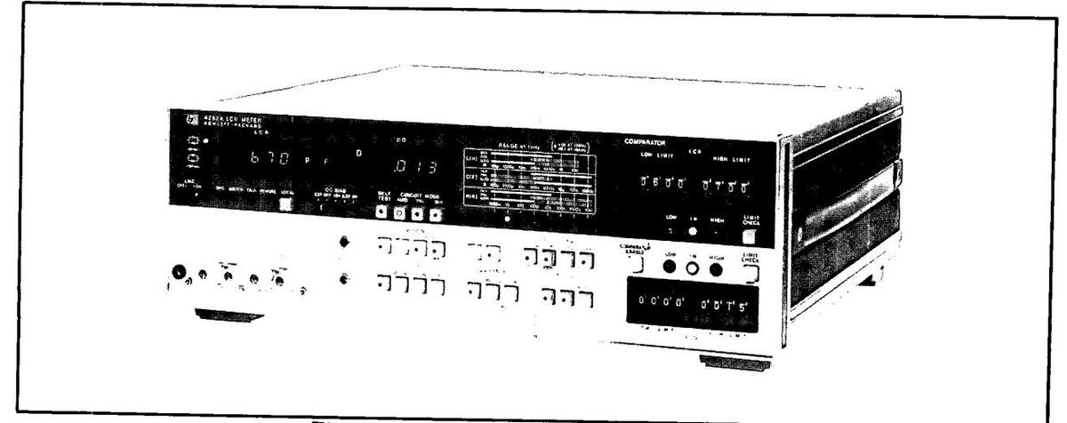
Figure 3-43. Option 004: COMPARATOR.
(7) COMPARATOR ENABLE Switch: This switch enables the Ontion 004 to compare measured data with HIGH and LOW limits under a fixed range condition (LCR or D/Q RANGE switch set to MANUAL) If LCR. RANGE switch or D/Q switch is set to AUTO, depressing COMPARATOR EN-ABLE switch changes LCR or D/Q RANGE switch setting to MANUAL. If AUTO key of LCR or D/Q RANGE
switch is depressed while COMPARATOR ENABLE switch is ON, one measurement cycle is done in AUTO ranging and the range is fixed to that selected in this measurement cycle.
2.52 LIMIT Setting Warning: If HIGH LIMIT setting is lower than LOW LIMIT setting. HIGH and LOW lamps of decision output repeatedly turn ON and OFF to warn operator to change LIMIT setting.
3-53. DATA OUTPUT Connector Decision Output: Decision outputs in TTL open collector signal and in relay contact are supplied through COMPARA-TOR OUTPUT connector on the rear panel. Signal pin assignment is given in Figure 3-44.
WARNING !
DO NOT APPLY AC LINE VOLT-AGE TO RELAY OUTPUT CON-NECTOR PIN TO SWITCH LINE CURRENT. For such relay applications, remotely control an external relay with relay output.
Relay Contact Ratings
| AC | DC | |
|---|---|---|
| Contact Resistance | 100mΩ | 100m Ω |
|
Maximum Permissible
Power |
30VA | 20W |
|
Maximum Permissible
Voltage |
110V | 30V |
|
Maximum Permissible
Current |
0.3A | 1A |
| Actuation Life | >10 million | >1 million |
Decision Output Data Format
| Decisions | Rela | y output | t pins | TTL output pins | ||
|---|---|---|---|---|---|---|
| Decisions |
DQ LCR
13 17 |
DQ LCR
14 18 |
DQ LCR
39 43 |
DQ LCR
15 19 |
DQ LCR
16 20 |
DQ LCR
41 45 |
| ні | S | s o o | н | L | L | |
| IN | 0 | 0 | o s | L | Н | |
| LO | 0 | S | 0 | L | Н | L |
S: Short O: Open
Referenced to common (pin 38 or 42). TTL Output sink current: 30mA max.

Figure 3-44. Comparator Data Output Pin Locations.
SectionIII Paragraphs 3-60 to 3-67
3-60. OPTION 101: HP-IB.
3-61. The 4262A Option 101 provides interface capabilities in accordance with IEEE-STD-488-1975 recommendations.
3-62. Connection to HP-IB Controller: The 4262A Option 101 can be connected to an HP-IB Controller (HP calculator) via HP-IB digital bus connector on the rear panel of the 4262A and the bus connector of the Bus I/O card installed in calculator.
3-63. HP-IB Status Indicator: The four LED lamps of the HP-IB Status Indicator (located below the LCR display) show which HP-IB condition the 4262A is in:
- SRQ: SRQ signal put on HP-IB line from 4262A. See paragraph 3-70 for details.
- LISTEN: 4262A is set to listen. See paragraph 3-69 for details.
- TALK: The 4262A is set to talk. See paragraph 3-67 for details.
- Remote: The 4262A is remotely controlled. See paragraph 3-71 for details.
3-64. LOCAL Switch: This switch disables remote control and enables setting measurement conditions by front panel controls (pushbutton switches). REMOTE lamp of HP-IB status indicator turns off when LOCAL switch is depressed. (When Local Lock Out does not function).
3-65. HP-IB INTERFACE CAPABILITIES: The 4262A Opt 101 has the following eight bus interface functions:
- SH1: Source Handshake Capability.
- AH1: Acceptor Handshake Capability.
- T5: Talker (the 4262A sends measurement data to the bus).
- L4: Listener (the 4262A receives remote control signals from the bus).
- SR1: Service Request Capability.
- RL1: Remote/Local Capability.
- DC1: Device Clear Capability.
- DT1: Device Trigger Capability.
- 3-66. Source and Acceptor Handshake: SH1, AH1.
Three Bus handshake lines (DAV, NRFD and NDAC) perform Source and/or Acceptor hand-shake functions.
- (1) DAV (DAta Valid). DIO (Data Input Output) line is available.
- (2) NRFD (Not Ready For Data). Listener preparation for receiving data from Talker is not yet completed.
- (3) NDAC (Not Data Accepted). Listener has not yet received data from Talker.
- 3-67. Talker Capability: T5.
When set to Talker by MTA (My Talk Address) signal from controller, the 4262A sends measurement data to the Bus in one of three types of output formats:
Type A: Ordinary output format. Address switch on the rear panel set to FMT A.
| S | FC | F | -NN. NNE-NN | I, SF | N.NNN | CRLF |
|---|---|---|---|---|---|---|
| (2) | (3) | (4) | (5)(1)(6) | (7) | (8) |
Type B: Output format used for Model 5150A HP-IB Digital Recorder. Address switch on the rear panel set to FMT B.
| S | FC F | -NN | NNE-NN | CRLF | SF | N.NNN | CRLF |
|---|---|---|---|---|---|---|---|
| · | |||||||
| (1) | (2) (3 | ) | (4) | (8) | (1)(6 | ) (7) | (8) |
-
Type C: Output format used in resistance measurement or LCR ONLY measurement when no D/Q data is to be outputted. Selection of this format is automatically done in accordance with FUNCTION switch setting.
- S FC F -NN. NNE-NN CRLF
The numbered elements of output data are described below:
(1) Status:
| N | Normal |
|---|---|
| 0 | Overflow |
| U | Uncal |
| X | LCRNA or DNA |
| (NA: Not Available) |
(2) Function and Circuit Mode:
| FUNCTION |
MEASURE-
MENT |
CIRCUIT
MODE |
|---|---|---|
| DDT | ||
| CP | C | PRL |
| CS | С | SER |
| LP | L | PRL |
| LS | L | SER |
| RP | R | PRL |
| RS | R/ESR | SER |
(3) Frequency:
A..... 120Hz (100Hz) B..... 1kHz C..... 10kHz
- (4) LCR Data
- (5) Data Delimiter
- (6) Loss
D..... Dissipation Factor measurement Q..... Quality Factor measurement
- (7) DQ Data
- (8) Data Terminator
-
3-68. Functions Related to Talker Capability.
- EOI (End Or Identify): When multiple byte data of Source Handshake has been sent, the 4262A provides EOI to the bus.
- Talk Only Mode: When ADDRESS switch is set to TALK ONLY "1" position, the 4262A is set to Talker regardless of address code.

Talk Address Disabled by Listen Address: MTA (My Talk Address) is automatically disabled when MLA (My Listen Address) is set. MTA (My Talk Address) is otherwise disabled by IFC (Interface Clear) signal, OTA (Other Talk Address) signal or UTA (Untalk Address) signal.
3-69. Listener Capability: L4.
To receive Remote Program signal or Addressed Command signal, the 4262A is set to Listener by an MLA (My Listen Address) signal from the bus.
- (1) Remote Program signal: Remote program codes for the 4262A are listed in Table 3-60.
-
(2) Addressed Command signal: When the 4262A receives command signals GET, GTL, or SDC, it is set to Listener and controlled by command signals. These command signals are valid regardless of the status (remote or local).
- GET (Group Execute Trigger): When the 4262A receives this command, it is triggered regardless of front panel TRIG-GER switch setting.
- GTL (Go to Local). The 4262A is set to LOCAL by this command to enable front panel control.
SDC (Selected Device Clear): When this command is accepted, front panel controls are set to initial conditions (the same conditions that are automatically set after turn-on of power switch).
Listen status is automatically disabled when MTA (My Talk Address) is received. Listen status is otherwise disabled by IFC (Interface Clear) signal or ULA (Unlisten Address) signal.
3-70. Service Request Capability: SR1.
The 4262A sends an SRQ (Service Request) signal whenever it is set in one of the six possible RQS (Request Status) states. It does this by responding to a serial poll of the controller by setting an STB (Staus Byte) signal on the bus. The 7th bit of this 8 bit signal establishes whether or not a service request exists. The remainder of the 8-bit signal identifies the character of the SRQ.

SRQ (Service Request) is disabled when RQS (Request Status) or STB (Status Byte) is set to 00000000 or when STB (Status Byte) signal transfer is completed.
Request Statuses (RQS) of the 4262A:
- (1) DRDY (Data ReaDY): When the 4262A completes a measurement cycle, this status bit is set. This status is set without serial polling if NOT DATA READY is set.
- (2) SYN ERR (SYNtax ERRor): When the 4262A receives an erroneous Remote Program Code which is not listed in Table 3-60, this status bit is set.
- (3) PASS (Self Test Pass): When PASS is displayed in Self Test done by remote control, this status bit is set.
- (4) FAIL 1 (Self Test Fail 1): When FAIL 1 is displayed in Self Test done by remote control, this status bit is set.
- (5) FAIL 2 (Self Test Fail 2): When FAIL 2 is displayed in Self Test done by remote control, this status bit is set.
- (6) FAIL 3 (Self Test Fail 3): When FAIL 3 is displayed in Self Test done by remote control, this status bit is set.
Table 3-60. Remote Program Codes.
| CONTRO | L | Program Code | ||
|---|---|---|---|---|
| Function | L | F 1 | ||
| С | F 2 | |||
| R⁄ | ´ES R | F 3 | ||
| Circuit Mode | AU | то | C 1 | |
| PR | L | C 2 | ||
| SE | R | C 3 | ||
| Loss | D | L 1 | ||
| Q | L 2 | |||
| Frequency | 120 | Hz | H 1 | |
| 1 k | Hz | H 2 | ||
| 10 | кHz | H 3 | ||
| Trigger | IN | Т | T 1 | |
| EX | Т | T 2 | ||
| НО | LD/MANU | JAL | Т 3 | |
| Self Test | OF | F | S 0 | |
| ON | S 1 | |||
| △LCR | OF | F | M 0 | |
| ON | M 1 | |||
| Cp Low Level | OF | F | P 0 | |
| ON | P 1 | |||
| *Data Ready | OF | F | D 0 | |
| RQS Mode | ON | D 1 | ||
| (C) | (L) | (R) | ||
| LCR Range | 100 p | 100 µ | 1000 m | R 1 |
| at 1 kHz | 1000 | 1000 | 10 | R 2 |
| 10 n | 10 m | 100 | R 3 | |
| 100 | 100 | 1000 | R 4 | |
| 1000 | 1000 | 10 k | _ R 5 | |
| 10 µ | 10 | 100 k | R 6 | |
| 100 | 100 | 1000 k | R 7 | |
| 1000 | - | 10 M | R 8 | |
| - AUTO - | _ | R 9 | ||
| DQ Range | (D) | (Q) | ||
| 1000 | N 1 | |||
| 100.0 | N 2 | |||
| 10.00 | 10.00 | N 3 | ||
| 1.000 | 1.000 | N 4 | ||
| _ | AUTO - | _ | N 5 | |
| * Data Ready RG | S Mode is au | tomatical | ly disabled w | hen Remote Status |
.
| CLASS |
D
I O 8 |
7 | 6 | 5 | 4 | 3 | 2 |
D
I O 1 |
||
|---|---|---|---|---|---|---|---|---|---|---|
| DCL | device clear | UC | x | 0 | 0 | 1 | 0 | 1 | 0 | 0 |
| GET | group execute trigger | AC | x | 0 | 0 | 0 | 1 | 0 | 0 | 0 |
| GTL | go to local | AC | x | 0 | 0 | 0 | 0 | 0 | 0 | 1 |
| LLO | local lock out | UC | x | 0 | 0 | 1 | 0 | 0 | 0 | 1 |
| MLA | my listen address | AD | x | 0 | 1 |
L
5 |
L
4 |
L
3 |
L
2 |
L
1 |
| МТА | my talk address | AD | x | 1 | 0 |
T
5 |
T
4 |
T
3 |
-
T 2 |
T
1 |
| ΟΤΑ | other talk address | AD | ( | ОТ | A = | = T. | AG | ۸M | TA | Ĵ |
| SDC | selected device clear | AC | x | 0 | 0 | 0 | 0 | 1 | 0 | 0 |
| SPD | serial poll disable | UC | x | 0 | 0 | 1 | 1 | 0 | 0 | 1 |
| SPE | serial poll enable | UC | x | 0 | 0 | 1 | 1 | 0 | 0 | 0 |
| STB | status byte | ST | s | х | S | S | S | S | S | S |
| UNL | unlisten | AD | x | 0 | 1 | 1 | 1 | 1 | 1 | 1 |
| UNT | untalk | AD | x | 1 | 0 | 1 | 1 | 1 | 1 | 1 |
| CLAS |
SS UC: Universal Command
AC: Addressed Command AD: Address ST: Status Byte |
• |
| Tabla | 3-61 | Remote | Massaga | Coding | |
|---|---|---|---|---|---|
| Table | 3-01. | Remote | message | Coung. |
Section III Paragraphs 3-71 to 3-75
3-71. Remote/Local Capability: RL1.
The 4262A goes to Remote Status only when it accepts Listen address with REN (Remote Enable) line in the Bus lines set to "1". Remote status is not obtained if REN line is set to "1" after Listen address is received. Remote status is returned to Local status when one of following conditions is present:
- (1) REN line is set to "0".
- (2) LOCAL switch on front panel is depressed.
- (3) GTL (Go To Local) command is received.
Local Lock Out: LLO
Local Lock Out inhibits the function of LOCAL switch. This LLO command is a universal command and is valid when REN line is set to "1". LLO command is disabled when REN line is set to "0"
3-72. Device Clear Capability: DC1.
The 4262A is set to initial conditions (the same conditions that are automatically set after turn-on of power switch), when it accepts DCL (Device CLear) command—universal command—or SDC (Selected Device Clear)—addressed command.
3-73. Device Trigger Capability: DT1.
The 4262A is triggered regardless of TRIGGER switch setting when it accepts GET command—ad-dress command.
3-74. ADDRESS Switch: ADDRESS switch on the rear panel sets Listen/Talk address. Five section or five bit switch provides 30 settings from 00000 to 11110.

3-75. Remote Message Coding: Interface Bus Command signals for the 4262A are listed in Table 3-61.
SECTION IV
PERFORMANCE TESTS
4-1. INTRODUCTION.
4-2. This section provides the check procedures to verify the 4262A specifications listed in Table 1-1. All tests can be performed without access to the interior of the instrument. A simpler operational test is presented in Section III under Self Test (paragraph 3-5). The performance test procedures in this section can also be used to do an incoming inspection of the instrument and to verify whether the instrument meets its specified performance after troubleshooting or making adjustments. If specifications are found to be out of limits, check that controls are properly set, and then proceed to adjustments or troubleshooting.
Note
Allow a 15-minute warm-up and stabilization period before conducting any performance test.
4-3. EQUIPMENT REQUIRED.
4-4. Equipment required for the performance tests is listed in Table 1-4 Recommended Test Equipment in Section I. Any equipment whose characteristics equal the critical specifications given in the table may be substituted for the recommended model(s).
Accuracy checks in this section use standard LCR components as the samples to be connected to the 4262A. Accessories 16361A and 16362A can be utilized for this purpose. These accessory models are DUT (device under test) boxes from which the desired component can be selected and connected to the 4262A through cables by use of a
rotary switch. If models 16361A/16362A are unavailable, use the discrete components recommended in Table 4-1.
Note
All components used as standards should be calibrated by an instrument whose specifications are traceable to NBS, PTB, LNE, NRC, JEMIC, or equivalent standards group; or all components should be calibrated directly by an authorized calibration organization such as NBS. The calibration cycle should be determined by the stability specification for each component.
4-5. TEST RECORD.
4-6. Results of the performance tests may be tabulated on the Test Record at the end of these procedures. The Test Record lists all the tested specifications and their acceptable limits. Test results recorded at incoming inspection can be used for comparison in periodic maintenance and troubleshooting and after repairs or adjustments.
4-7. CALIBRATION CYCLE.
4-8. This instrument requires periodic verification of performance. Depending on the use and environmental conditions, the instrument should be checked with the following performance tests at least once every year. To maximize the "up time" of the instrument, the recommended preventive maintenance frequency for the 4262A is twice a year.
--------------------------------------
Before beginning performance test, adjustment, or calibration of 4262A, check fundamental operating conditions of the instrument and perform display ZERO adjustments in accord with the following procedures:
- 1) Confirm that power line power voltage in use is appropriate for the instrument operating power voltage.
- 2) Depress LINE pushbutton and confirm that all the front panel displays and indicators momentarily illuminate. The 4262A functions are automatically set to capacitance measurement mode.
-
3) ZERO offset adjustment should be made whenever a test fixture or DUT box is connected to 4262A UNKNOWN terminals. Adjust C ZERO ADJ and L ZERO ADJ controls so as to fully compensate for stray capacitance and residual inductance of equipment connected to UNKNOWN terminals. Adjustment procedures to adjust for individual test equipment used are provided in steps 3-a and 3-b which follow.
-
3-a) 16361A/16362A or user built DUT box.
- 1. Disconnect shorting bars from 4262A UNKNOWN terminals. Connect test leads between 4262A UNKNOWN terminals and DUT box.
- 2. Set 4262A FUNCTION to C. Set TEST SIGNAL frequency as appropriate to DUT box being used.
- 3. Set range control of DUT box to open-circuit position (2pF range on 16361A or 1pF range on 16362A). The 4262A is automatically set to its lowest capacitance measurement mode range.
- 4. Adjust C ZERO ADJ control so that capacitance readout on 4262A LCR display is identical to calibrated value of DUT box range.
-
5. Set 4262A FUNCTION to L.
- 6. Set range control of DUT box to short-circuit position (20mΩ range on 16361A or on 16362A).
- 7. Adjust L ZERO ADJ control for 000 counts on LCR display.
-
3-a) 16361A/16362A or user built DUT box.
Note
To permit easy adjustment of ZERO ADJ controls for an individual DUT box, each DUT box should be equipped with short and open circuit ranges which provide 0µH and 0pF (practical values), respectively.
--------------------------------------
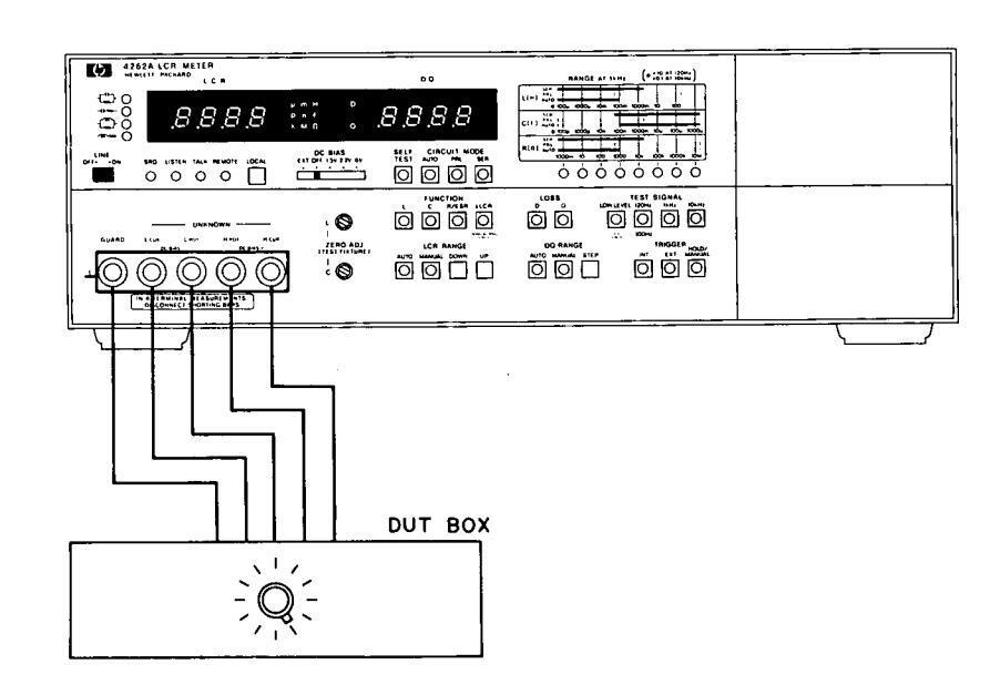
3-b) 16061A or other test fixtures.
- 1. Disconnect shorting bars from 4262A UNKNOWN terminals and attach test fixture to UNKNOWN.
- 2. No DUT should be connected to the test fixture.
- 3. The 4262A is automatically set to lowest capacitance range in measurement mode. Set 4262A TEST SIGNAL frequency to 10kHz.
- 4. Adjust C ZERO ADJ control for 000 counts on LCR display.
- 5. Set 4262A FUNCTION to L.
- 6. Connect a shorting lead to test fixture to short-circuit the measurement terminals.
- 7. Adjust L ZERO ADJ control for 000 counts on LCR display.
Note
When positions or mutual distance between Test Fixture contacts are changed, or contacts are changed to a different type, again perform ZERO adjustments.
-- CALIBRATION OF DUT'S-
Either user built DUT's or substitution standards with accuracies which satisfy the requirements may be used for performance testing and calibration of the 4262A. The DUT's recommended for making the tests and adjustments can be accuracy certified in accord with the calibration procedure detailed below. This calibration procedure applies to all alternate DUT's which do not carry public or testing laboratory certification.
[CAPACITANCE CALIBRATION]
Measure the DUT or substitution standard capacity with a precision capacitance bridge that meets the calibration accuracy and frequency requirements. For testing or calibrating dissipation factor of DUT, use equipment with required dissipation measuring capability and verify the exact calibration frequency to permit compensating D value for the difference in measuring frequency between individual Model 4262A's and the calibration equipment. If the frequency error is less than 3%, compensation is not required for dissipation factors of 0.01 and below.
[RESISTANCE CALIBRATION]
Use a metal film resistor of appropriate value for each DUT to maintain a constant resistance over a wide range of frequencies. Measure the resistance with a high accuracy DMM. When measuring 1kΩ and below, use a 4 terminal measurement configuration.
[DISSIPATION FACTOR CALIBRATION]
DUT's used as D standards can be built with precisely measured components. The dissipation factor of the DUT is determined by an exact calculation from the calibrated values of each components in accord with the following equations:
| Circuit Mode | Derivation of D |
|---|---|
| D = 1/\omega CpRp | |
|
Cs Rs
IIW |
D = \u03c6CsRs |
Note
For easier calibration of dissipation, use accurately calibrated resistors rather than capacitors.
----- CALIBRATION OF DUT'S -
To minimize the calculation error, the inherent dissipation of the capacitor should be 0.001 or below. When using polystyrene or silvered mica type capacitors (dissipation factor is generally very low), the residual factors will not affect the derivation of accurate dissipation factors. If dissipation of capacitor alone is greater than 0.001, the effective value of the DUT is calculated in accord with the following equation:
Ds = Dc + Dr (Dr < Dc, Dr < 0.01)
where, Ds is actual dissipation factor of DUT. Dc is calculated D value (excludes inherent dissipation). Dr is inherent dissipation of capacitor.
Compensate the dissipation factor for the measuring frequencies of individual 4262A being tested or calibrated. Convert the D value of the calibration frequency to that of the actual 4262A measuring frequency in accord with the following equations:
| -[" | x = |
Dm: D value at 4262A
measuring frequency. Ds: D value at calibration frequency. |
|
|---|---|---|---|
| Dm = X · Ds | ⊣⊦₩ |
x =
fm
fc |
fm: 4262A measuring
frequency fc: Calibration frequency. |
Note
To accurately measure frequencies fm and fc, use a reciprocal counter or calculate reciprocal number of period.
[CALIBRATION EQUIPMENT]
The recommended model and required performance of calibration equipment is listed below:
| Instrument | Required Performance | Recommended Model |
|---|---|---|
| Capacitance Bridge |
Capacitance Accuracy: 0.1%
Dissipation Factor Accuracy: 0.1% (Resolution 0.0001) |
GR 1620-A |
| DMM | Resistance Accuracy: 0.02% |
HP 3490A
HP 3455A |
| Freq. Counter |
Reciprocal counter
Resolution: 0.01Hz |
HP 5300A/5307A
HP 5323A |
Section IV Table 4-1
| 14010 1-1. 1000 | ||||
|---|---|---|---|---|
| Comp | onent *1 | HP Part Number | Alternate Source |
Required
Calibration Accuracy |
| Capacitor |
100pF
1000pF 10nF 100nF 1000nF 10μF 1000μF 10mF |
0160-0336
0160-3766 0160-0408 0160-1571 0160-3645 0160-3563 |
HP Model 4440B
GR Type 1413 SOSHIN TM-520C GR Type 1417 |
0.05%
0.2% 0.25% |
| Resistor: |
1kΩ
10kΩ 100kΩ 10MΩ |
0698-3491
0698-6360 0698-4158 0698-8194 |
GR Type 1433-Y | 0.05% |
| Inductor: | 100mH | GR Type 1482-L | 0.05% | |
|
Dissipation Fact
1000nF in p (D≈1. 100nF in par (D≈1. 10nF in para (D≈1.) |
or:
parallel with 887Ω 50 at 120Hz) rallel with 887Ω 79 at 1kHz) allel with 887Ω 79 at 10kHz) |
0160-3645
0698-4464 0160-1571 0698-4464 0160-3171 0698-4464 |
(D=1/ωCR) |
**2
Capacitors • 0.1% Resistors • 0.02% |
Table 4-1. Recommended Components for Accuracy Checks.
*1 The components listed above or used as standards should be calibrated before they are utilized.
**2 For easier calibration of dissipation to the required accuracy (0.1%), use accurately calibrated resistors rather than capacitors (use a high accuracy DMM to measure resistors).
Proper method and procedure for calibrating the DUT's is given in "Calibration of DUT's" (Page 4-4).
4-9. MEASUREMENT FREQUENCY TEST.
DESCRIPTION:
This test verifies the accuracy of the measurement frequencies that are applied to an unknown sample connected to the 4262A.
SPECIFICATIONS:
| 1 | |
|---|---|
| leasurement Frequencies: | 120Hz ± 3% |
| _ | 1kHz + 3% |
1kHz ± 3%
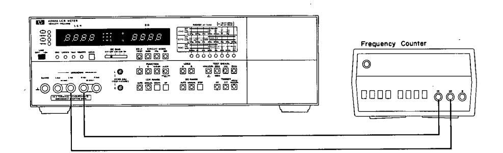
Figure 4-1. Measurement Frequency Test Setup.
EQUIPMENT:
Frequency Counter ....................................
PROCEDURE:
- 1. Connect frequency counter to the 4262A UNKNOWN terminals as shown in Figure 4-1.
- 2. Set range of frequency counter as appropriate for measuring 4262A test frequencies of 120Hz, 1kHz and 10kHz.
- 3. Read display output of frequency counter when 4262A TEST SIGNAL is set to 120Hz, 1kHz or 10kHz.
- 4. Frequency readouts must be within the following limits (record measured frequency in table below as the data is used in paragraph 4-12):
| TEST SIGNAL | Test Limits | Counter Readout |
|---|---|---|
| 120Hz | 116.4 - 123.6Hz | |
| 1kHz | 970 - 1030 Hz | |
| 10kHz | 9700 - 10300 Hz |
Note
Test limits in table above do not take into account reading error caused by measurement error in test equipment.
Note
If this test fails, refer to Service Sheet 11 in Section VIII for troubleshooting.
4-10. CAPACITANCE ACCURACY TEST.
DESCRIPTION:
This test checks capacitance measurement accuracy for zero and full scale displays at three test frequencies and at two signal levels. The test is made by connecting a stable capacitor more accurate than the 4262A to the instrument and reading the display to verify that the 4262A meets its measurement accuracy specifications. Check all ranges in Cp mode and one range in Cs mode at each frequency (120Hz, 1kHz and 10kHz) to guarantee C measurement accuracy since all variable elements (range resistors and detecting phases) needed for C measurement are thus checked. In this test, almost all ranges, from the lowest through the highest ranges, are being verified.
Note
If the following tests satisfy the accuracy specifications, all the accuracy specifications listed in Table 1-1 are guaranteed.
Capacitance Accuracy Test Ranges
| TEST | SIGNAL | CIRCUIT | RANGE | ||||||
|---|---|---|---|---|---|---|---|---|---|
| Freq. | Level | MODE | 10.00pF | 100.0pF | 1000pF | 10.00n F | 100.0nF | 1000n F | 10.00µF |
| LOW LEVEL | PRL | × | × | ||||||
| 120Hz | normal | PRL | X | ||||||
| nonna | SER | × | ⊳< | × | × | × | |||
| LOW LEVEL | PRL | × | × | ||||||
| 1kHz | PRL | Х | ⊠ | ||||||
| normal | SER | Х | Х | × | × | ||||
| LOW LEVEL | PRL | - | × | × | |||||
| 10kHz | PRL | S | ∽ | ||||||
| normal | SER | × | Х | × | ~ | ~ `` |
TEST SIGNAL level:
| LOW LEVEL |
|
٠ | • | • | 50 | mV | ||||||||
|---|---|---|---|---|---|---|---|---|---|---|---|---|---|---|
| normal |
• |
• | • | • | • | • | • | • | • | • | •• | 1V |
Tests for dissipation factor accuracy with above capacitance standards should be done at the same time as capacitance tests
Check all parallel (PRL) mode ranges. It is sufficient to check any one range in series (SER) mode.

Figure 4-2. Capacitance Accuracy Test Setup.
SPECIFICATIONS:
| Range |
120Hz
1kHz 1kHz 10kHz |
1000pF10.00nF100.0nF 1000nF10.00μF 100.0μF 1000μF 10.00mI
100.0pF 1000pF10.00nF100.0nF 1000nF 10.00μF 100.0μF 1000μF 10.00pF 100.0pF 1000pF 10.00nF 100.0nF 1000nF 10.00μF 100.0μF |
|---|---|---|
| -417- |
0.2% + 1 count
(Test signal level: 1V)
0.5% +
3 count 0.3% + 2 counts (Test signal level: 50mV) |
|
| C Accuracy*1 | -11 | (At 120Hz, 1kHz) 0.3% + 2 counts 0.5% + 2 counts 1% + *2 2 counts (At 10kHz) 0.3% + 2 counts 1% + 2 5% + 2 |
| AUTO | Same as -L- Mode Same as -I+ Mode | |
|
D (1/Q)
Accuracy *1 |
-$$}- | 0.2% + (2 + 200/Cx) counts At 120Hz, 1kHz 0.5% + (2 + 200/x) counts (Test signal level: 1V) 0.3% + (2 + 1000/Cx) counts At 120Hz, 1kHz 1.0% + (2 + 1000/Cx) counts (Test signal level: 50mV) At 10kHz At 10kHz |
|
(At 120Hz, 1kHz)
(At 10kHz) 0.5% + (2 + Cx/500) counts 1% + (5 + Cx/500) counts 1% + (5 + Cx/500) counts 1% + (5 + Cx/500) counts 1% + (5 + Cx/500) counts 1% + (5 + Cx/500) counts 1% + (5 + Cx/500) counts 1% + (5 + Cx/500) counts 1% + (5 + Cx/500) counts 1% + (5 + Cx/500) counts 1% + (5 + Cx/500) counts 1% + (5 + Cx/500) counts 1% + (5 + Cx/500) counts 1% + (5 + Cx/500) counts 1% + (5 + Cx/500) counts 1% + (5 + Cx/500) counts 1% + (5 + Cx/500) counts 1% + (5 + Cx/500) counts 1% + (5 + Cx/500) counts 1% + (5 + Cx/500) counts 1% + (5 + Cx/500) counts 1% + (5 + Cx/500) counts 1% + (5 + Cx/500) counts 1% + (5 + Cx/500) counts 1% + (5 + Cx/500) counts 1% + (5 + Cx/500) counts 1% + (5 + Cx/500) counts 1% + (5 + Cx/500) counts 1% + (5 + Cx/500) counts 1% + (5 + Cx/500) counts 1% + (5 + Cx/500) counts 1% + (5 + Cx/500) counts 1% + (5 + Cx/500) counts 1% + (5 + Cx/500) counts 1% + (5 + Cx/500) counts 1% + (5 + Cx/500) counts 1% + (5 + Cx/500) counts 1% + (5 + Cx/500) counts 1% + (5 + Cx/500) counts 1% + (5 + Cx/500) counts 1% + (5 + Cx/500) counts 1% + (5 + Cx/500) counts 1% + (5 + Cx/500) counts 1% + (5 + Cx/500) counts 1% + (5 + Cx/500) counts 1% + (5 + Cx/500) counts 1% + (5 + Cx/500) counts 1% + (5 + Cx/500) counts 1% + (5 + Cx/500) counts 1% + (5 + Cx/500) counts 1% + (5 + Cx/500) counts 1% + (5 + Cx/500) counts 1% + (5 + Cx/500) counts 1% + (5 + Cx/500) counts 1% + (5 + Cx/500) counts 1% + (5 + Cx/500) counts 1% + (5 + Cx/500) counts 1% + (5 + Cx/500) counts 1% + (5 + Cx/500) counts 1% + (5 + Cx/500) counts 1% + (5 + Cx/500) counts 1% + (5 + Cx/500) counts 1% + (5 + Cx/500) counts 1% + (5 + Cx/500) counts 1% + (5 + Cx/500) counts 1% + (5 + Cx/500) counts 1% + (5 + Cx/500) counts 1% + (5 + Cx/500) counts 1% + (5 + Cx/500) counts 1% + (5 + Cx/500) counts 1% + (5 + Cx/500) counts 1% + (5 + Cx/500) counts 1% + (5 + Cx/500) counts 1% + (5 + Cx/500) counts 1% + (5 + Cx/500) counts 1% + (5 + Cx/500) counts 1% + (5 + Cx/500) counts 1% + (5 + C |
||
| AUTO | Same as |
C-D/Q MEASUREMENT ACCURACIES.
*1 ±(% of reading + counts). Cx is capacitance readout in counts. This accuracy only applies for D values to 1.999.
*2 (5% +2 counts) at 1kHz.
Accuracy applies over a temperature range of 23°C ±5°C (at 0°C to 55°C, error doubles).
EQUIPMENT:
DUT Box..... HP 16361A/16362A Test Leads...... HP P/N 16361-61605
Note
User built test fixture or DUT box may be used instead of those HP provides. If user supplied, the residual impedance and stray capacitance of the fixture and box must be taken into account.
PROCEDURE:
- 1. Connect Test Leads (HP P/N 16361-61605) between 4262A UNKNOWN terminals and HP 16361A DUT Box (see Figure 4-2). When TEST SIGNAL frequency is 10kHz, use HP 16362A in place of HP 16361A.
- 2. Set 4262A controls as follows:
| DC BIAS | ÷ | • | C | )F | ٢F | ||||||||||||||
|---|---|---|---|---|---|---|---|---|---|---|---|---|---|---|---|---|---|---|---|
| FUNCTION | С | ||||||||||||||||||
| LCR RANGE | • | • | A | Ū | JT | Ó | |||||||||||||
| LOSS | D | ||||||||||||||||||
| D/Q RANGE. | • | А | U | Л | 0 | ||||||||||||||
| TRIGGER | ••• | • | • | • | • | • | • | IN | IT |
PERFORMANCE TESTS
3. Confirm that the table on page 4-11 is satisfied when the measurements are made by changing TEST SIGNAL, CIRCUIT MODE and DUT as given in the table. Record capacitance and dissipation factor readings in blank spaces provided in table.
Note
Error caused by stability of standard component is not taken into account for test limits in the table.
Test limits in parentheses are those for dissipation factor measurement value.
If tests fail, proceed to Section V ADJUSTMENTS or Section VIII SERVICE.
4
.
PERFORMANCE TESTS
| TEST | TEST SIGNAL CIRCUIT | 16361 | A/16362A | RANGE | |||||||
|---|---|---|---|---|---|---|---|---|---|---|---|
| Freq. | level | MODE | 10pF*1 | 100pF | 1000pF | 10nF | 100nF | 1000nF | 10µF | 1000µF | 10mF |
|
LOW
LEVEL |
PRL |
C. V.
±4 counts () |
C. V.
±8 counts () |
C. V.
±5 counts (±3 counts) |
C. V.
±5 counts (±3 counts) |
C. V.
±5 counts (±3 counts) |
C. V.
±5 counts (±3 counts) |
||||
| 120Hz | PRL |
C. V.
±2 counts (±4 counts) |
C. V.
±3 counts (±3 counts) |
C. V.
±3 counts (±3 counts) |
C. V.
±3 counts (±3 counts) |
C. V.
±3 counts (±3 counts) |
C. V.
±3 counts (±3 counts) |
||||
| normal | SER |
C. V.
±3 counts (±3 counts) |
C. V.
±5 counts (±4 counts) |
C. V.
±5 counts (±4 counts) |
C. V.
±7 counts (±4 counts) |
C. V.
±12 count (±7 count |
|||||
|
LOW
LEVEL |
PRL |
C. V.
±8 counts () |
C. V.
±5 counts (±3 counts) |
C. V.
±5 counts (±3 counts) |
C. V.
±5 counts (±3 counts) |
C. V.
±5 counts (±3 counts) |
|||||
| 1kHz | PRL |
C. V.
±3 counts (±3 counts) |
C. V.
±3 counts (±3 counts) |
C. V.
±3 counts (±3 counts) |
C. V.
±3 counts (±3 counts) |
C. V.
±3 counts (±3 counts) |
|||||
| normal | SER | L | I |
C. V.
±3 counts (±3 counts |
C. V.
±5 counts ) (±4 counts) |
C. V.
±5 counts (±4 counts) |
C. V.
±5 counts (±4 counts) |
C. V.
±52 counts (±7 counts) |
|||
|
LOW
LEVEL |
PRL |
C. V.
±8 counts () |
C. V.
±5 counts (±4 counts |
C. V.
±5 counts (±3 counts |
C. V.
±5 counts (±3 counts) |
C. V.
±5 counts ) (±3 counts) |
1 | I | L | ||
| 10kHz | PRL |
C. V.
±3 counts (±3 counts) |
C. V.
±3 counts )(±3 counts |
C. V.
±3 counts (±3 counts |
C. V.
±3 counts ) (±3 counts |
C. V.
±3 counts ) (±3 counts) |
|||||
| normal | SER |
C. V.
±3 counts (±3 counts |
C. V.
s±5 counts ) (±4 counts |
C. V.
s ±5 counts )) (±4 counts |
C. V.
s±5 counts )(±4 counts |
C. V.
s ±12 counts ) (±7 counts |
s | ||||
*1 HP 16362A Only **2 C. V. = Calibrated Value of Standard Component.
4-11. RESISTANCE/**ESR ACCURACY TEST.
DESCRIPTION:
This test verifies that resistance measurement accuracies for 4262A tested meets the specifications listed below. Although R measurement accuracies are actually guaranteed when C measurement accuracies meet the specifications, almost all ranges in Rp mode are checked in this test.
Note
Resistance accuracy has only to be proved for one resistor of about full scale value on any one range to verify specifications for 120Hz, 1kHz and 10kHz.
SPECIFICATION:
| ~ | 10110 | |||||||||
|---|---|---|---|---|---|---|---|---|---|---|
| Ranges |
120Hz
1kHz 10kHz |
1000mΩ | 10.00Ω | 100.0Ω | 1000Ω | 10.00kΩ | 100.0kΩ | 1000kΩ | 10.00MΩ | |
| L | 0.39 | % + 2 cou | nts *2 | |||||||
| Accuracy *1 | 11 | 0.2% + 2 counts | ||||||||
| AUTO | Sam | e as -II | Iode | Same a | s -C | - Mo | de | |||
RESISTANCE/ESR ACCURACY SPECIFICATIONS
*1 ±(% of reading + counts).
*2 (5% +2 counts) on 10.00MΩ range at 10kHz.
** Measurement range for ESR (equivalent series resistance) is from 1mΩ to 19.99kΩ (typical), which varies with series capacitance or inductance value .... refer to "REFERENCE DATA" on page 1-6.
Accuracy applies over a temperature range of 23°C ±5°C, (at 0°C to 55°C, error doubles).
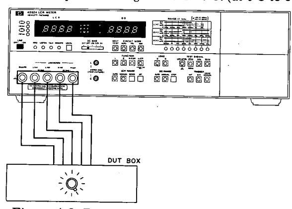
Figure 4-3. Resistance Accuracy Test Setup
EQUIPMENT:
DUT Box. .
Note
User built fixture/leads or DUT box can be used. If user supplied, the residual resistance must be considered.
PROCEDURE:
- 1. Connect Test Leads (HP P/N 16361-61605) between 4262A UNKNOWN terminals and HP 16361A DUT Box (see Figure 4-3).
- 2. Set 4262A controls as follows:
| DC BIAS | OFF |
|---|---|
| CIRCUIT MODE | PRL |
| FUNCTION | . R/ESR |
| LCR RANGE | . AUTO |
| TEST SIGNAL | 1kHz |
| TRIGGER | INT |
3. Check that the resistance measurement accuracies meet specifications according to table below:
| DUT | 1kΩ | 10kΩ | 100kΩ | 10 ΜΩ |
|---|---|---|---|---|
| Test Limits |
C. V.
±5 counts |
C. V.
±5 counts |
C. V.
±5 counts |
C. V.
±5 counts |
| R Readout |
C. V. = Calibrated Value of Standard Component
Note
Error caused by stability of standard component is not taken into account for test limits in table above.
Note
If this test fails, go to Section V or Section VIII for the troubleshooting.
Model 4262A
4-12. DISSIPATION FACTOR CONFIRMATION CHECK
DESCRIPTION:
This test verifies that a tested 4262A satisfies dissipation factor measurement accuracies. Only one Dissipation Factor (D = 1.8) is checked for 120Hz, 1kHz and 10kHz in this check because only one detecting phase needs to be checked. All other factors influencing D accuracy were checked in paragraph 4-10.
Note
Dissipation factor accuracy for only one D standard which has a D value of approximately 1.8 need be proved to guarantee D accuracy. This test also verifies that 4262A correctly calculates Q factor as a reciprocal number of Dissipation Factor. Only one Q factor corresponding to a D value of approximately 1.8 is checked in this test. D accuracy in measuring inductance does not need to be checked because detecting phase accuracy is equated with that for capacitance measurement.
C-D ACCURACY SPECIFICATIONS
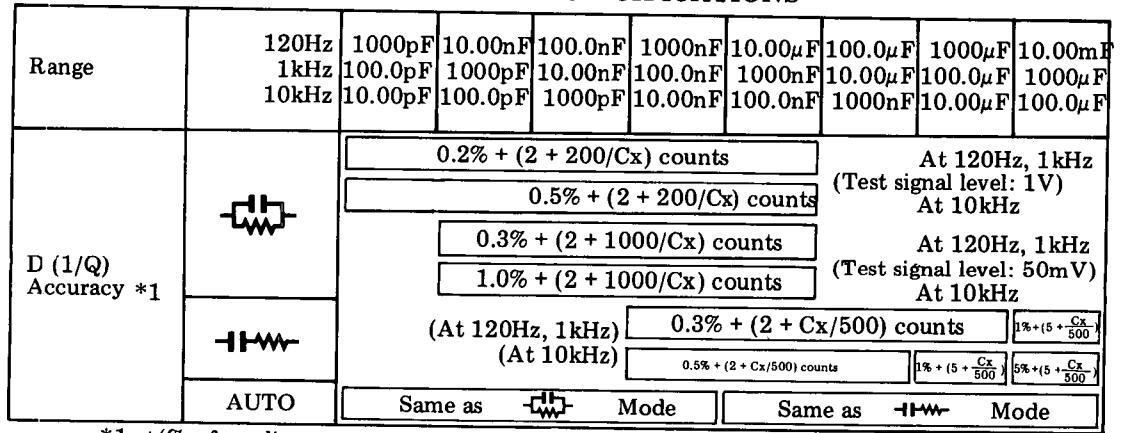
*1 ±(% of reading + counts). Cx is capacitance readout in counts.
Accuracy applies over temperature range of 23°C ±5°C. (At 0°C to 55°C, error doubles) This accuracy only applies for D values to 1.999.
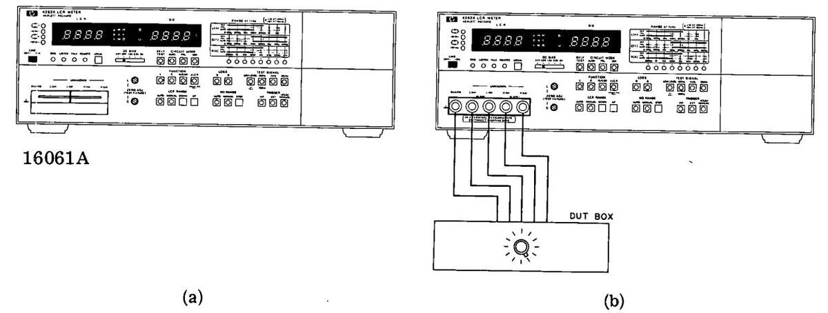

EQUIPMENT:
| Test Fixture | HP 16061A |
|---|---|
| DUT | HP 16361A/16362A |
| Test Leads | HP P/N 16361-61605 |
Note
HP 16361A and HP 16362A DUT Boxes are equipped with D standards (D = 1.8) calibrated at 1kHz and 10kHz frequencies, respectively. For the test at 120Hz frequency or if DUT box is not available, it is recommended that the following DUT's be used as D standards:
| DUT | Freq. | Values of components | Calculated D | Tolerance* |
|---|---|---|---|---|
| С | 120Hz |
C :1000nF(HP P/N 0160-3645)
R : 887Ω (HP P/N 0698-4464) |
1.495 | ±0.030 |
| 1kHz |
C : 100nF (HP P/N 0160-1571)
R : 887Ω (HP P/N 0698-4464) |
1.794 | ±0.036 | |
| R | 10kHz |
C : 10nF (HP P/N 0160-3171)
R . 887Ω (HP P/N 0698-4464) |
1.794 | ±0.036 |
* After calibrating capacitance C to within 0.1% and resistance R to within 0.02%, the dissipation factor tolerance is ±0.002 for each DUT.
PROCEDURE:
1. Connect DUT to 4262A.
Note
To facilitate connecting recommended DUT's, attach HP 16061A Test Fixture to 4262A UNKNOWN terminals [see Figure 4-4 (a)]. When HP 16361A/16362A DUT Box is used for this test, connect Test Leads (HP P/N 16361-61605) between 4262A UNKNOWN terminals and DUT Box as shown in Figure 4-4 (b).
2. Set 4262A controls as follows:
| DC BIAS | OFF |
|---|---|
| CIRCUIT MODE | PRL |
| FUNCTION | C |
| LOSS | D |
| LCR RANGE | AUTO |
| D/Q RANGE | AUTO |
| TRIGGER | INT |
PERFORMANCE TESTS
3. Check D accuracies according to following table:
| Freq | Circuit Mode | Test Level | D Test Limits | D Reading |
|---|---|---|---|---|
| _ _ _┩┡╼ ┣ | Low Level | Calibrated Value X ± 8 counts | ···· | |
| 120Hz | L | normal | Calibrated Value X ± 6 counts | |
| normal | Calibrated Value X ± 8 counts | |||
| ⊣⊢ _ | Low Level | Calibrated Value X ± 8 counts | ||
| 1 kHz | normal | Calibrated Value X ± 6 counts | ||
| normal | Calibrated Value X ± 9 counts | |||
| _ _+⊢ | Low Level | Calibrated Value X ± 21 counts | ||
| 10kHz | normal | Calibrated Value X ± 11 counts | ||
| normal | Calibrated Value X ± 13 counts |
Note
X in above table is produced by test frequency error and may be determined from the following equations:
••• where fn is nominal measurement frequency and fx is measurement frequency from paragraph 4-9.
Note
Error caused by stability of standard component is not taken into account for test limits in table above.
4. Set 4262A TEST SIGNAL frequency to 1kHz and connect appropriate DUT to 4262A (Set 16361A LCR RANGE to D = 1.8). Note dissipation readout on D/Q display.
5. Push 4262A LOSS Q button.
6. Confirm that displayed Q factor is correct reciprocal number of dissipation.
Note
The 4262A rounds fractions of 5 or greater below the LSD to the next higher digit and drops any fractions of 4 or less. For example, if the actual dissipation is .0135, the display will read .014. If the actual dissipation is .0134, the display will read .013. If the test fails, refer to Section VIII Service.
Paragraph 4-13
Section IV
4-13. INDUCTANCE ACCURACY TEST.
DESCRIPTION:
This test verifies that inductance measurement accuracy satisfies the specifications listed below. L accuracy is proved to meet the specification when the results obtained in the accuracy checks of paragraphs 4-9 through 4-12 satisfy the specifications. This test is performed to confirm the L accuracy specification.
Note
Inductance accuracy has only to be proved for one inductor of about full scale value on any one range to verify specifications for all three test frequencies (120Hz, 1kHz and 10kHz).
SPECIFICATIONS:
| Range |
120Hz
1kHz 10kHz |
1000µН
100.0µН 10.00µН |
10.00mH
1000µH 100.0µH |
100.0mH
10.00mH 1000µH |
1000mH
100.0mH 10.00mH |
10.00H
1000mH 100.0mH |
100.0H
10.00H 1000mH |
1000H
100.0H 10.00H |
|||
|---|---|---|---|---|---|---|---|---|---|---|---|
| -∰- | (At 120 |
)Hz, 1kHz)
At 10kHz) |
0.3% + 2 |
2 counts
2 counts |
1% + 2 counts 1% + 2 5% + 2 | ||||||
| L Accuracy | 0.2 | 2% + 2 cour | nts | (At 120Hz | , 1kHz) | ||||||
| *1 | 0.3% + 2 0.2% + 2 counts (At 10kHz) | ||||||||||
| AUTO | Sau | meas | Same a | is -())- | Mode | ||||||
INDUCTANCE ACCURACY SPECIFICATIONS
*1 ±(% of reading + counts).
Accuracy applied over temperature range of 23°C ±5°C (at 0°C to 55°C, error doubles). This accuracy only applies for D values to 1.999.
Figure 4-5 Inductance Accuracy Test Setup.
EQUIPMENT:
DUT Box..... HP 16361A/16362A Test Leads..... HP P/N 16361-61605
Note
User built test fixture/leads or DUT box must take residual impedance into consideration.
PROCEDURE:
- 1. Connect Test Leads (HP P/N 16361-61605) between 4262A UNKNOWN terminals and HP 16361A DUT Box (see Figure 4-5). When TEST SIGNAL frequency is 10kHz, use HP 16362A in place of HP 16361A.
- 2. Set 4262A controls as follows:
| DC BIAS | • | • | 0 | F | F | |||||||||||||
|---|---|---|---|---|---|---|---|---|---|---|---|---|---|---|---|---|---|---|
| FUNCTION | • | • | • | • | . 1 | L | ||||||||||||
| LOSS | •. | • | I | D | ||||||||||||||
| LCR RANGE | A | U' | Г | ) | ||||||||||||||
| D/Q RANGE. | • | A | U | го | C | |||||||||||||
| TRIGGER | • | • | D | N' | Г |
3. Set HP 16361A/16362A LCR RANGE to 100mH.
4. Confirm that L accuracy is within the test limits shown in table below:
Note
Test limits below are given for 100mH inductance measurement. If another inductance value is measured, refer to SPECIFICATIONS above.
|
TEST SIG
Freq. |
CIRCUIT
MODE |
TEST Limits | L Readout |
|---|---|---|---|
| 19047 | PRL | Calibrated Value ± 3 counts | |
| 120112 | SER | Calibrated Value ± 4 counts | |
| 112117 | PRL | Calibrated Value ± 5 counts | |
| IKIIZ | SER | Calibrated Value ± 4 counts | |
| 10247 | PRL | Calibrated Value ± 5 counts | |
| TONIZ | SER | Calibrated Value ± 4 counts |
Note
Error caused by stability of standard component is not taken into account for test limits in table above. If this test fails, refer to Section VIII,Service.
4-14. INTERNAL DC BIAS SOURCE TEST.
DESCRIPTION:
This test verifies that the internal dc bias source will apply the specified bias values to the device under test.
SPECIFICATIONS:
DC bias, Internal Source: 1.5V ±5%, 2.2V ±5%, 6V ±5%
Figure 4-6. Internal DC Bias Source Test Setup.
EQUIPMENT:
DC Voltmeter ...... HP 5300A/w5306A
PROCEDURE:
1. Connect DC Voltmeter to 4262A UNKNOWN terminals as shown in Figure 4-6.
2. Set 4262A controls as follows:
| FUNCTION | • | • | ( | С | |||||||||||||
|---|---|---|---|---|---|---|---|---|---|---|---|---|---|---|---|---|---|
| CIRCUIT MODE. | • | • | ٠ | PI | RI | L | |||||||||||
| Other Controls | a | n | v | р | ю | s | iti | 01 | n |
Note
Do not connect anything to UNKNOWN terminals.
3. Test limits are shown below. Read dc voltmeter output with DC BIAS switch set as follows:
|
DC BIAS
Switch Setting |
Test Limits | Voltmeter Readout |
|---|---|---|
| 1.5V | 1.425V thru 1.575V | |
| 2.2V | 2.09 V thru 2.31 V | |
| 6 V | 5.7 V thru 6.3 V | - |
Note
Reading error caused by measurement error of test equipment is not taken into account for test limits in table above.
4. If tests fail, proceed to Troubleshooting in Section VIII.
4-15. OFFSET ADJUSTMENT TEST.
DESCRIPTION:
This test checks that both C and L ZERO ADJ controls can be set (over their specified ranges) to respectively offset the stray capacitance and residual inductance of test jig.
SPECIFICATIONS:
| Offset Adjustment: | C:up to 10pF |
|---|---|
| L:up to 1µH |
EQUIPMENT:
DUT Box..... HP 16362A (19pF) Test Leads....................................

Figure 4-7. Offset Adjustment Test Setup.
PROCEDURE:
(1) C ZERO ADJ test.
- 1. Connect shorting bars at 4262A UNKNOWN terminals for doing a two terminal measurement. Connect no DUT to unknown terminals (open).
- 2. Set 4262A controls as follows:
| CIRCUIT MODE AUTO |
| FUNCTION |
| LOSSD |
| FEST SIGNAL 10kHz |
| LCR RANGEMANUAL |
| (Set to 10pF range) |
| DQ RANGE AUTO |
| FRIGGER INT |
- 3. Rotate C ZERO ADJ control fully cw.
- 4. Verify that capacitance readout on 4262A LCR display is within 0.00 to 0.30 counts.
- 5. Disconnect shorting bars from 4262A UNKNOWN terminals and connect Test Leads (HP P/N 16361-61605) between 4262A UNKNOWN terminals and 16362A DUT Box as shown in Figure 4-7.
Note
If 16362A is not available, connect an 18pF capacitor (HP P/N 0160-2263) directly to UNKNOWN terminals (without disconnecting shorting bars).
6. Set 16362A LCR RANGE to 19pF.
- 7. Note capacitance readout on 4262A LCR display.
- 8. Rotate C ZERO ADJ control fully ccw.
- 9. Verify that capacitance readout on 4262A LCR display reduces count more than 10.30 counts as compared to count obtained in step 7.
- 10. Remove Test Leads (or DUT) from UNKNOWN terminals.
(2) L ZERO ADJ test
- 11. Set 4262A FUNCTION to L.
- 12. Connect shorting bars on 4262A UNKNOWN terminals for doing a two terminal measurement. Connect a shorting lead to UNKNOWN terminals so that H and L terminals are short circuited.
- 13. Rotate L ZERO ADJ control fully cw.
- 14. Verify that inductance readout on 4262A LCR display is within 0.00 and 0.02 counts.
- 15. Disconnect shorting lead from 4262A UNKNOWN terminals and connect a 5.6µH inductor (HP P/N 9100-1618) directly to UNKNOWN terminals as a DUT (without disconnecting shorting bars).
- 16. Note inductance readout on 4262A LCR display.
- 17. Rotate L ZERO ADJ control fully ccw.
- 18. Verify that inductance readout on 4262A LCR display reduces count more than 1.02 counts as compared to count obtained in step 16.

PERFORMANCE TESTS
4-16. COMPARATOR TEST (OPTION 004 ONLY).
DESCRIPTION:
This test verifies that the built-in 5 digit digital comparator makes the correct comparison between the digits set into the thumbwheel switch and the displayed counts. Comparison output data at COMPARATOR OUTPUT connector (rear panel) is also checked by this test.
Figure 4-8. Comparator Test Setup.
EQUIPMENT:
DUT Box..... HP 16361A (100pF) Test Leads..... HP P/N 16361-61605
PROCEDURE:
- 1. Connect Test Leads (HP P/N 16361-61605) between 4262A UNKNOWN terminals and 16361A DUT Box as shown in Figure 4-8. If DUT Box is not available, attach 16061A Test Fixture to 4262A UNKNOWN terminals and use a 100pF capacitor as a DUT.
- 2. Set 4262A controls as follows:
| BIAS | • | •• | OI | F | |||||||||||||||||||
|---|---|---|---|---|---|---|---|---|---|---|---|---|---|---|---|---|---|---|---|---|---|---|---|
| RCUIT | ' MO | DE | • | • | • | • | Α | UΊ | O | ||||||||||||||
| NCTIO | ON | • • | • | С | |||||||||||||||||||
| ST SIC | GNA | L. | • | • | . 1 | lkł | Ηz | ||||||||||||||||
| R RAI | NGE | • | • | • | A | UI | Ο | ||||||||||||||||
| IGGE | R | •• | • | • | • • | • | • | • | • • | • | • | • | • | • | • | • | •• | IN | IT | ||||
|
BIAS
RCUIT NCTI( ST SIC R RAN IGGE |
BIAS
CUIT MO NCTION ST SIGNA R RANGE IGGER |
BIAS
RCUIT MODE NCTION ST SIGNAL . R RANGE IGGER |
BIAS | BIAS | BIAS | BIAS | BIAS | BIAS | BIAS | BIAS | BIAS | BIAS | BIAS | BIAS | BIAS |
BIAS
RCUIT MODE NCTION ST SIGNAL R RANGE IGGER |
BIAS | BIAS | BIAS | BIAS |
BIAS OF
RCUIT MODE AUT NCTION |
BIASOFF
CUIT MODEAUTO NCTIONC ST SIGNALIkHz R RANGEAUTO IGGERINT |
- 3. Set 16361A LCR RANGE to 100pF.
- 4. Push COMPARATOR ENABLE button (simultaneously, the LCR RANGE and DQ RANGE will be automatically changed to MANUAL).
- 5. Set LCR HIGH LIMIT switch to "1000" and LOW LIMIT switch to "0950".
- 6. Verify HIGH and LOW LIMIT settings by pushing and holding upper LIMIT CHECK pushbutton.
- 7. Adjust ZERO ADJ C control for a display reading of "949" (or less) counts.
PERFORMANCE TESTS
- 8. LOW lamp should be lit. Verify circuit configuration on COMPARATOR OUT-PUT connector (J6) according to Figure 4-9.
- 9. Adjust ZERO ADJ C control cw for a display reading of "950" (up to "999").
- 10 IN lamp should be lit. Verify relay contact and TTL output as in step 8.
- 11 ADJUST ZERO ADJ C control cw for a display reading of "1000" or more.
- 12 HIGH lamp should be lit. Verify relay contact and TTL output as in step 8.
- 13. Set 16361A LCR RANGE to D = 1.8 and 4262A LCR RANGE manually to 1µF.
Note
If HP 16361A is not available, use a D factor sample as shown below.
| C: 100nF (HP P/N 0160-4113) | |
|---|---|
| Lw L | R: 887Ω (HP P/N 0698-4464) |
14. Push D/Q RANGE AUTO button.
Note
The 4262A D/Q RANGE is automatically set to an appropriate range and successively reset to MANUAL.
15. Set appropriate numbers into D/Q LIMIT switches. Change the set numbers and check comparison outputs with Figure 4-9.


Figure 4-9. DATA OUTPUT (J6) comparator output data format.
4-17. HP-IB INTERFACE TEST (OPTION 101 ONLY).
DESCRIPTION:
This test verifies that the HP-IB circuitry has the capability to correctly communicate between external HP-IB devices and the 4262A through the interface bus cable.
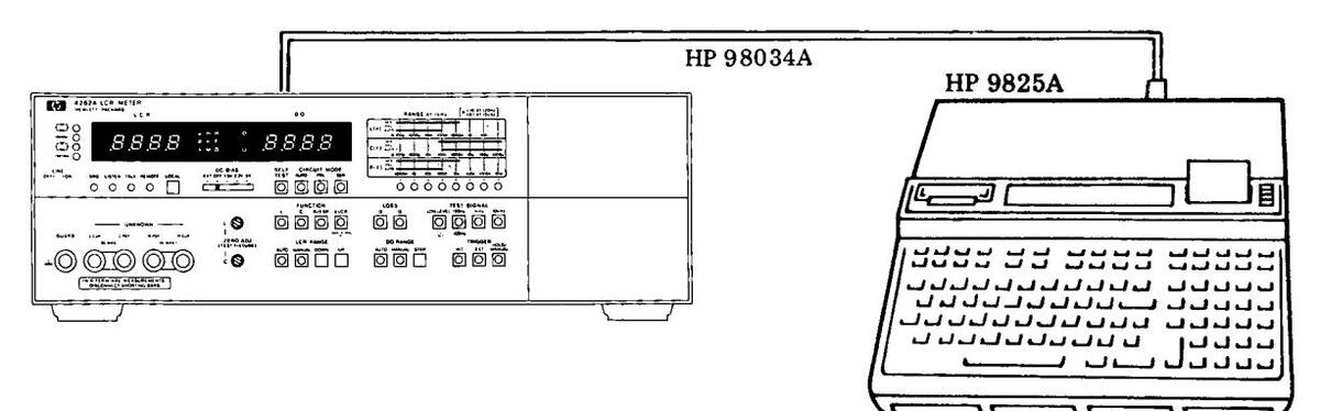
Figure 4-10. HP-IB Interface Test Setup.
EQUIPMENT:
| Calculator | HP 9825A |
|---|---|
| ROM | HP 98210A, |
| 98213A or 98214A | |
| Interface Card with cable | HP 98034A |
PROCEDURE:
- 1. Connect 98034A Interface Card with cable between 9825A I/O slot and 4262A rear panel HP-IB connector. Install required ROM blocks in 9825A ROM slots.
- 2. Set 98034A Select Code Switch dial to select code 7 (using a screwdriver).
- 3. Set 4262A rear panel ADDRESS switch to address number 17 in binary code (refer to Paragraph 3-68).
- 4. Load test program (shown on Pages 4-26 through 4-35) in calculator.
- 5. Execute the program. Check that 4262A display, calculator display, and printed data are consistent with the results described for each program.
- 6. Perform steps 4 and 5 with respect to individual test programs and verify that 4262A and calculator correctly communicate through the HP-IB interface.
Note
Connect appropriate sample(s) to 4262A UNKNOWN terminals as necessary (and observe whether printout is correct).
[PURPOSE]
This test verifies that system controller remotely sets 4262A TEST SIGNAL and TRIGGER and successively accesses the measured data for printing.
[PROGRAMMING]
0: prt "MEASURED DATA
    RECEIVED"; spc 3
1: dev "4262A",717
2: rem 7
3: cli 7
4: clr "4262A"
5: wrt "4262A","H3T3"; wait 1000
6: trg "4262A"
7: red "4262A", A, B
8: flt 3
9: prt "LCR DATA=",A,
    "DQ DATA=",B
10: spc 3
11: end
*32657
0) Commands calculator to print MEASURED DATA RECEIVED and successively to space three lines.
Madal 4969 A
- Defines 717 (= Interface Select Code 7, address 17) as address code for 4262A in the programming.
- 2) Sets REN (Remote Enable) line of the Bus line to "1". Enables remote control.
- 3) Sets IFC (Interface Clear) line of Bus line to "1". Sets interface select code 7 to its initial conditions.
- 4) Sets 4262A to its initial conditions. (Device Clear: ref to Para 3-72).
- 5) Addresses calculator to talk and 4262A to listen. Program code string sets device: TEST SIGNAL 10kHz, and TRIGGER to HOLD/MANUAL (ref to Para 3-69).
- 6) Triggers 4262A (ref to Para 3-73).
- 7) Addresses calculator to listen and 4262A to talk. Takes incoming data and stores LCR measurement data in register A and DQ data in register B (ref to Para 3-67).
- 8) Designates printer print format and floating decimal point (3 digits below decimal point).
- 9) Prints LCR and DQ data.
- 10) Commands printer to line space three vertical lines to put entire recording into proper cutting position.
[RESULTS]
The 4262A REMOTE lamp lights. LISTEN and TALK lamps alternately light once. Calculator prints measured LCR and DQ values.
[PURPOSE]
This test verifies that system controller sets 4262A TEST SIGNAL and TRIGGER and prints the measured data along with the 4262A functional status codes.
[PROGRAMMING]
0: prt " MEASURED DATA RECEIVED ";spc 3
1: rem 7
2: cli 7
3: clr 717
4: wrt 717,"H3P1T3":wait 1000
5: trg 717
6: fmt 4b.f.2b.f
7: red 717.A.B.C.D.E.F.G.H
8: fxd 0:prt "S=".A."F=".B.
  "C=",C,"F=",D
9: flt 3:prt "N=".E
10: fxd 0:prt "S=",F,"F=",G
11: flt 3:prt "N=".H
12: spc 3
13: end
*15961
- 3) Sets device address code 717 (4262A) for initial conditions.
- 4) Addresses calculator to talk and device of address code 717 (4262A) to listen. Program code string sets device TEST SIGNAL to 10kHz, LOW LEVEL, and TRIGGER to HOLD/MAN-UAL (ref to Table 3-60).
- 6) Designates format for data in program step 7.
- 7) Addresses calculator to listen and 4262A to talk. Takes incoming data A, B, C, D, F and G in binary code and translates them into decimal code. Takes data E and H in free field format. Stores data items in the registers specified in the variable lists.
- 8-11) Prints data in fixed or floating decimal point format. Data items are:
| A: Status, | B: Function, |
|---|---|
| C: Circuit Mode, | D: Frequency, |
| E: LCR Data, | F: DQ Status, |
| G: DQ Function, | H: DQ Data. |
Refer to Paragraph 3-67 and Table 3-60.
[RESULTS]
The 4262A REMOTE lamp lights. LISTEN and TALK lamps alternately light once. Calculator prints 4262A functional codes along with the measured LCR and DQ data.
PERFORMANCE TESTS
TEST PROGRAM 3
[PURPOSE]
This test verifies that 4262A notifies system controller of the Request Status (RQS) and that demands of the Service Request (SRQ) are processed according to programmed service routing.
[PROGRAMMING]
0: prt "MEASURED DATA RECEIVED -DATA READY ROS MODE":spc 3
l: oni 7."SRO"
2. rom 7
                                     1) Designates label (SRQ) for service routing to be
3: cli 7
                                        performed when an interrupt is set by a device
4: clr 717
                                        on select code 7 Bus Line.
5: wrt 717."H3D1T3";wait 1000
6: tra 717
7: "LOOP":eir 7,128
8: if bit(0.B)=1:gto "READ"
9: ato "LOOP"
10: "SRO":rds(717)+B
                                     5) Addresses calculator to talk and 4262A to listen
11: if bit(6.B)=1; jmp 2
                                        Program code string set device: TEST SIGNAL
12: prt "OTHER DEVICE SRO":spc 3
                                        10kHz, Data Ready RQS Mode to ON (ref to
13: "IRET":eir 7,128
                                        Para 3-70), and TRIGGER to HOLD/MANUAL.
14: iret
15: "READ":red 717,A,B
16: flt 3;prt "LCR DATA=".A.
                                     7) Labels LOOP. Enables Service Request to be
    "DO DATA=" B
                                        sent from device on select code 7 Bus Line
17. spc 3
                                        Checks status of SRQ line on the Bus Line.
18. and
*22913
                                     8) If the last bit of Status Byte (corresponding to
                                        Data Ready — ref to Para 3-70) is 1 goes to pro-
Note
gram step 15 labeled READ.
When status of the SRQ line becomes 1, the programming sequence phase changes from cycling through steps 7, 8, and 9 and successively goes to step 10. Steps 10 through 14 comprise the service routing to process interrupt (Service Request) phase. See Figure 4-11 for programming flow diagram.
- 10) Labels SRQ. Takes Status Byte responding to serial poll of calculator and stores data in register B.
- 11) Verifies that SRQ YES/NO line of Status Byte is actually 1 (ref to Para 3-70).
- 13) Again enables acceptance of SRQ from device because SRQ is disabled when Status Byte signal transfer is completed (re to Para 3-70).
- 14) After service subroutine is completed, return to the step that follows step 7, 8, or 9 as appropriate to main programming sequence.
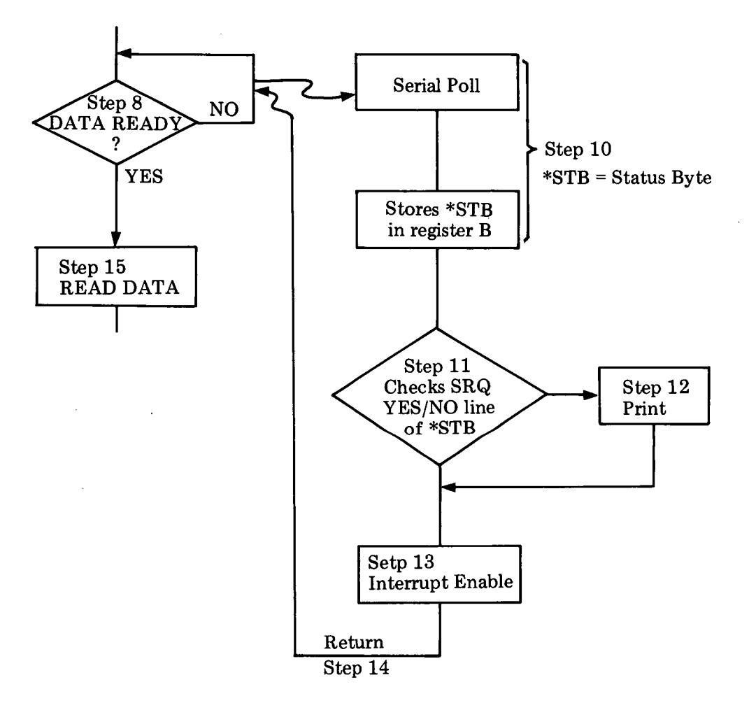
Figure 4-11 SRQ Service Routing.
[RESULTS]
Calculator prints LCR and DQ values of the sample measured by 4262A (test frequency 10kHz). Verifies that 4262A SRQ lamp lights momentarily. Press calculator RUN button again to repeat checks. If calculator prints OTHER DEVICE SRQ, interface is faulty.
[PURPOSE]
This test confirms that 4262A FUNCTION, LOSS, and TEST SIGNAL functions are fully controlled by system controller.
[PROGRAMMING]
Annotation is omitted 0: prt "ENTER REMOTE PROGRA1 CODE ":spc 3 1: fmt 1.4f1.0 2 . rom 7 3: cli 7 4: clr 717 5: ent "FUNCTION?(1.2.3)".A 6: ent "LOSS?(1,2)",B 7: ent "FREQUENCY?(1.2.3)".C 8: wrt 717.1, "F", A, "L", B, "H", C, "T3"; wait 1000 9: tra 717 10: red 717.D.E 11: flt 3:prt "LCR DATA=",D,"DO DATA=",E 12: spc 3 13: end *31495
[RESULT]
The 4262A REMOTE lamp lights. LISTEN and TALK lamps alternately light once. Calculator prints LCR and DQ values. Confirms that 4262A functions were correctly set (check the printed data).
(PURPOSE)
This test verifies that 4262A self test function can be remotely controlled.
[PROGRAMMING]
0: prt "REMOTE SELF TEST"; spc 3
1: •oni 7."SRO"
2: rem 7
3: cli 7
4: clr 717
5: wrt 717."S1"
6: "[OOP":eir 7.128
7: if bit(2.A)=1:dsp "PASS"
3: if bit(3.A)=1:dsp "FAIL 1"
9: if bit(4,A)=1:dsp "FAIL 2"
10: if bit(5,A)=1:dsp "FAIL 3"
11: ato "LOOP"
12: "SRO":beep:rds(717)+A
13: if bit(6,A)=1:ato "IRET"
14: prt "OTHER DEVICE
    SRO"; spc 3
15: "TRET":eir 7.128
16: iret
17: end
*14058
[RESULT]
5) Addresses calculator to talk and 4262A to listen. Sets device to SELF TEST mode.
7, 8, 9, 10)
Checks status of the third through sixth bit of Status Byte signal and displays its contents (ref to Para 3-70).
12) Labels SRQ. Takes Status Byte responding to serial poll of calculator and stores data in register A. Simultaneously beeps in announcement.
The 4262A performs self test. Letters "PASS" flash on both 4262A and calculator displays.
[PURPOSE]
This test verifies that system controller takes the incoming data in character (ASCII) code and prints the data in accord with the format shown in Paragraph 3-67.
[PROGRAMMING]
0: prt "RECEIVING MEASURED DATA when using STRING-ADV. ROM":spc 3
1: dim AS[25]
2: rem 7
3. cli 7
                                    1) Establish dimension of 25 character memory
4: clr 717
                                       capacity for using string variables
5: wrt 717."H3T3";wait 1000
6: tra 717
7: red 717.AS
8: prt AS
9. spc 3
10: end
                                    7) Takes incoming data (measured data) in charac-
*671
                                       ter (ASCII) code.
8) Prints data in character code.
[RESULT]
The measured data and 4262A functional status code are printed in accord with the format shown in Paragraph 3-67.
PERFORMANCE TESTS
TEST PROGRAM 7
[PURPOSE]
This test verifies that 4262A FUNCTION, FREQUENCY and TRIGGER can be controlled in character (ASCII) code and that the measured data is printed in accord with the format shown in Paragraph 3-67.
[PROGRAMMING]
Annotation is omitted.
0: prt "ENTER REMOTE PROGRAM CODE when using STRING-ADV ROM";spc 3 1: dim A$[20],B$[25] 2: rem 7 3: cli 7 4: ent "PROGRAM CODE ? (as F2H3T3)",A$ 5: wrt 717,A$;wait 1000 6: trg 717 7: red 717,B$ 8: prt B$ 9: spc 3 10: end *3337 [RESULTS]
The 4262A REMOTE lamp lights. LISTEN and TALK lamps alternately light once. Calculator prints LCR and DQ values. Confirms that 4262A functions were correctly set (check the printed data).


 Loading...