

Page 1

User’s Reference
Publication number 16550-97006
August 1997
For Safety information, Warranties, and Regulatory
information, see the pages behind the Index
• Copyright Hewlett-Packard Company 1992 – 1998
All Rights Reserved
HP 16550A
100-MHz State/500-MHz Timing
Logic Analyzer
Page 2

ii
Page 3

In This Book
The User’s Reference contains field and
feature definitions. Use this manual for
information on what the menu fields do,
what they are used for, and how the
features work.
The manual is divided into chapters
covering general product information,
probing, and separately tabbed chapters
for each analyzer menu. Also, chapters
on error messages and instrument
specifications are provided.
In the Configuration menu you have the
choice of configuring an analyzer as
either a State analyzer or a Timing
analyzer. Some menus in the analyzer
will change depending on the analyzer
type you choose. For example, since a
Timing analyzer does not use external
clocks, the clock assignment fields in the
Format menu will not be available.
If a menu field is only available to a
particular analyzer type, the field is
designated (Timing only) or (State only)
after the field name. If no designation is
shown, the field is available for both
types.
1
General Information
2
Probing
3
The Configuration Menu
4
The Format Menu
5
The Trigger Menu
6
The Listing Menu
7
The Waveform Menu
8
The Chart M enu
9
The Compare Menu
10
The Mixed Display Menu
11
Error Messages
Specifications and
12
Characteristics
13
Installation and Testing
Index
iii
Page 4

iv
Page 5

Table of Contents
1 General Information
Configuration Capabilities 1–3
Key Features 1–4
Accessories Supplied 1–5
Accessories Available 1–6
2 Probing
General Purpose Probing System Description 2–7
Assembling the Probing System 2–11
3 The Configuration Menu
Name Field 3–3
Type Field 3–4
Unassigned Pods List 3–5
Activity Indicators 3–7
4 The Format Menu
State Acquisition Mode Field (State only) 4–4
Timing Acquisition Mode Field (Timing only) 4–5
Clock Inputs Display 4–13
Pod Field 4–14
Pod Clock Field (State only) 4–15
Pod Threshold Field 4–19
Master and Slave Clock Field (State only) 4–20
Setup/Hold Field (State only) 4–22
Symbols Field 4–24
Label Assignment Fields 4–24
Rolling Labels and Pods 4–24
Label Polarity Fields 4–25
Bit Assignment Fields 4–26
Contents–1
Page 6

Contents
5 The Trigger Menu
Trigger Sequence Levels 5–6
Modify Trigger Field 5–8
Pre-defined Trigger Macros 5–11
Using Macros to Create a Trigger Specification 5–13
Timing Trigger Macro Library 5–14
State Trigger Macro Library 5–16
Modifying the User-level Macro 5–19
Resource Terms 5–26
Assigning Resource Term Names and Values 5–28
Label and Base Fields 5–32
Arming Control Field 5–33
Acquisition Control 5–36
Trigger Position Field 5–37
Sample Period Field 5–38
Branches Taken Stored / Not Stored Field 5–38
Count Field (State only) 5–39
6 The Listing Menu
Markers Field 6–4
Pattern Markers 6–5
Find X-pattern / O-pattern Field 6–6
Pattern Occurrence Fields 6–7
From Trigger / Start / X Marker Field 6–8
Specify Patterns Field 6–9
Label / Base Roll Field 6–12
Stop Measurement Field 6–13
Clear Pattern Field 6–16
Contents–2
Page 7

Time Markers 6–17
Trig to X / Trig to O Fields 6–18
Statistics Markers 6–19
States Markers (State only) 6–21
Trig to X / Trig to O Fields 6–22
Data Roll Field 6–23
Label and Base Fields 6–24
Label / Base Roll Field 6–24
7 The Waveform Menu
Acquisition Control Field 7–5
Accumulate Field 7–6
States Per Division Field (State only) 7–7
Seconds Per Division Field (Timing only) 7–8
Delay Field 7–9
Sample Period Display (Timing only) 7–10
Markers Field 7–12
Contents
Pattern Markers 7–13
X-pat / O-pat Occurrence Fields 7–14
From Trigger / Start / X Marker Field 7–15
X to O Display Field (Timing only) 7–16
Center Screen Field 7–17
Specify Patterns Field 7–18
Label / Base Roll Field 7–21
Stop Measurement Field 7–22
Clear Pattern Field 7–25
Time Markers 7–26
Trig to X / Trig to O Fields 7–27
Marker Label / Base and Display 7–28
Contents–3
Page 8

Contents
Statistics Markers 7–29
States Markers (State only) 7–31
Trig to X / Trig to O Fields 7–32
Marker Label / Base and Display 7–33
Waveform Display 7–34
Blue Bar Field 7–36
Channel Mode Field 7–38
Module and Label Fields 7–40
Action Insert/Replace Field 7–41
Delete and Delete All Fields 7–42
Waveform Size Field 7–43
8 The Chart Menu
Selecting the Axes for the Chart 8–6
Y-axis Label Value Field 8–7
X-axis Label / State Type Field 8–8
Scaling the Axes 8–9
Min and Max Scaling Fields 8–10
Markers / Range Field 8–11
Pattern Markers 8–12
Find X-pattern / O-pattern Field 8–13
Pattern Occurrence Fields 8–14
From Trigger / Start / X Marker Fields 8–15
Specify Patterns Field 8–16
Label / Base Roll Field 8–18
Stop Measurement Field 8–19
Clear Pattern Field 8–22
Contents–4
Page 9

Time Markers 8–23
Trig to X / Trig to O Fields 8–24
Statistics Markers 8–25
States Markers 8–27
Trig to X / Trig to O Fields 8–28
9 The Compare Menu
Reference Listing Field 9–5
Difference Listing Field 9–6
Copy Listing to Reference Field 9–8
Find Error Field 9–9
Compare Full / Compare Partial Field 9–10
Mask Field 9–11
Specify Stop Measurement Field 9–12
Data Roll Field 9–15
Bit Editing Field 9–16
Label and Base Fields 9–17
Label / Base Roll Field 9–17
Contents
10 The Mixed Display Menu
The Mixed Display Menu 10–2
Intermodule Configuration 10–3
Inserting Waveforms 10–4
Interleaving State Listings 10–5
Time-Correlated Displays 10–7
Markers 10–8
Contents–5
Page 10

Contents
11 Error Messages
Error Messages 11–3
Warning Messages 11–6
Advisory Messages 11–9
12 Specifications and Characteristics
Specifications 12–3
Characteristics 12–4
13 Installation and Testing
To inspect the module 13–3
To prepare the mainframe 13–3
To configure a one-card module 13–5
To configure a two-card module 13–6
To install the module 13–8
To test the module 13–10
To perform the self-tests 13–10
To clean the logic analyzer module 13–12
Index
Contents–6
Page 11

1
General Information
Page 12

Logic Analyzer Description
The HP 16550A State/Timing Analyzer module is part of a new
generation of general-purpose logic analyzers. The HP 16550A
module is used with the HP 16500B/C mainframe, which is designed
as a stand-alone instrument for use by digital and microprocessor
hardware and software designers. The HP 16500B/C mainframe has
HP-IB and RS-232-C interfaces for hard copy printouts and control by
a host computer.
The HP 16550A State/Timing Analyzer module has 96 data channels,
and six clock/data channels. A second HP 16550A card can be added
to expand the module to 204 data and clock/data channels.
Memory depth is 4 Kbytes in all pod pair groupings, or 8 Kbytes on
just one pod (half channels). All resource terms can be assigned to
either configured analyzer machine.
Measurement data is displayed as data listings or waveforms, and can
be plotted on a chart or compared to a reference image.
The 100-MHz state analyzer has master, slave, and demultiplexed
clocking modes available. Measurement data can be stamped with
either state or time tags. For triggering and data storage, the state
analyzer uses 12 sequence levels with two-way branching, 10 pattern
resource terms, 2 range terms, and 2 timers/counters.
The 500-MHz timing analyzer has conventional, transitional, and glitch
timing modes with variable width, depth, and speed selections.
Sequential triggering uses 10 sequence levels with two-way branching,
10 pattern resource terms, 2 range terms, 2 timers/counters and 2
edge/glitch terms.
Defining a trigger specification is as easy as picking a predefined
macro from a trigger macro library. Trigger macros can be used by
themselves or in combination with each other.
1–2
Page 13
State Analyzer
General Information
Configuration Capabilities
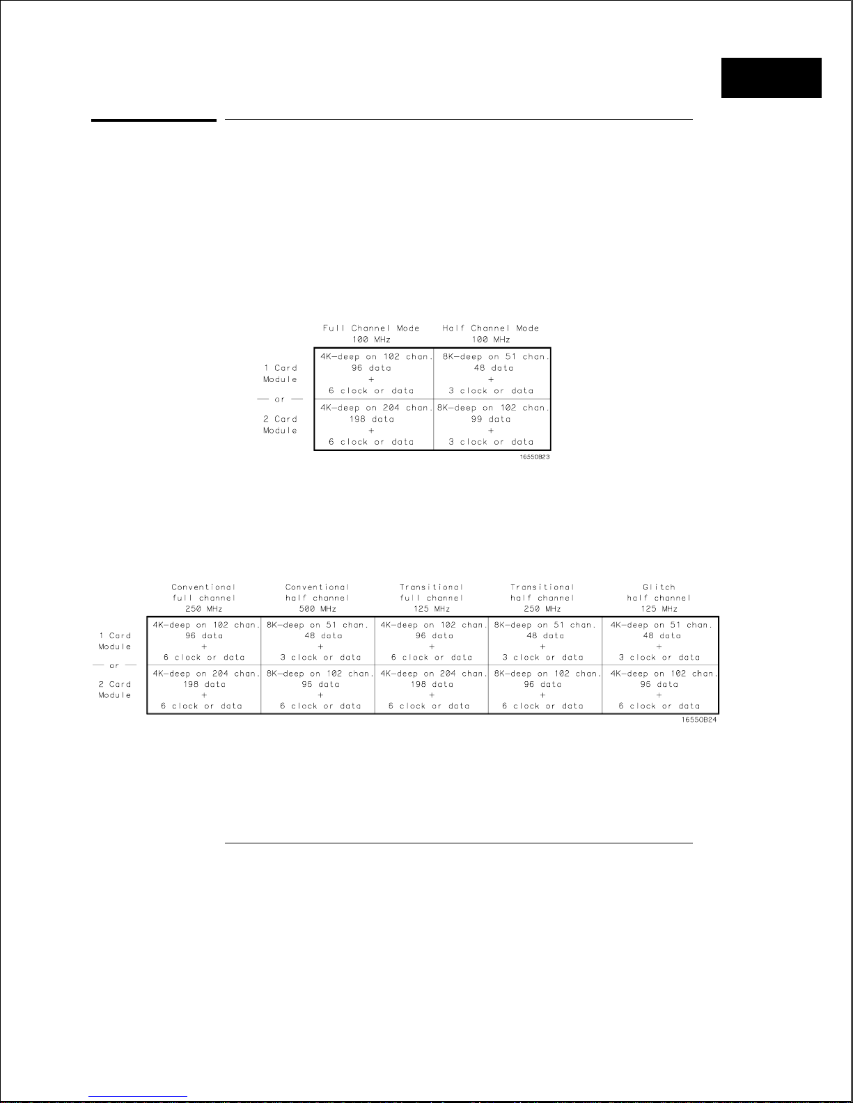
Configuration Capabilities
The HP 16550A can be configured as a single- or two-card module. The
number of data channels range from 102 channels using just one HP 16550A,
up to 204 channels when a second HP 16550A is connected. A half-channel
acquisition mode is available which reduces the channel width by half, but
doubles memory depth from 4K-deep to 8K-deep per channel.
The configuration guide below illustrates the channel width and memory
depth combinations in all acquisition modes with a one or two card module.
Timing Analyzer
Unused clock channels can be used as data channels
•
Time or State tags reduces memory by half. However, full depth is
•
retained if you leave one pod pair unassigned.
Maximum of 6 clocks in a two-card module.
•
Unused clock channels can be used as data channels
•
1–3
Page 14

General Information
Key Features
Key Features
100-MHz state and 500-MHz timing acquisition speed.
•
96 data/6 clock channels, expandable to 198 data/6 clock channels.
•
Lightweight passive probes for easy hookup and compatibility with
•
previous HP logic analyzers and preprocessors.
Variable setup/hold time, 3.5 ns window.
•
External arming to/from other modules through the intermodule bus.
•
4 Kbytes deep memory on all channels with 8 Kbytes in half channel
•
modes.
Marker measurements.
•
12 levels of trigger sequencing for state and 10 levels of sequential
•
triggering for Timing.
Both state and timing analyzers can use 10 pattern resource terms, two
•
range terms, and two timer/counters to qualify and trigger on data. The
timing analyzer also has two edge terms available.
Predefined trigger macros for easy configuration of trigger specifications.
•
100-MHz time and number-of-states tagging.
•
Full programmability.
•
Mixed State/Timing and State/State (interleaved) display.
•
Compare, Chart, and Waveform displays.
•
1–4
Page 15

General Information
Accessories Supplied
Accessories Supplied
The table below lists the accessories supplied with your logic analyzer. If any
of these accessories are missing, contact your nearest Hewlett-Packard Sales
Office. If you need additional accessories, refer to the Accessories for HP
Logic Analyzers brochure.
Table 1-1
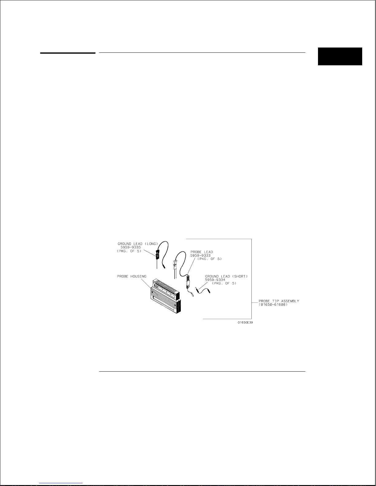
Accessories Supplied
Accessory HP Part No. Quantity
Probe tip assemblies 01650-61608 6
Probe cables 16550-61601 3
Grabbers (20 per pack) 5090-4356 6
Extra probe leads (5 per pack) 5959-9333 1 pkg
Probe cable and pod labels 01650-94310 1
Probe cable ID clip 16500-41201 1
Operating system disks Call 1
User’s Reference Call 1
1–5
Page 16

General Information
Accessories Available
Accessories Available
There are a number of accessories available that will make your measurement
tasks easier and more accurate. You will find these listed in Accessories for
HP Logic Analyzers.
Preprocessor Modules
The preprocessor module accessories enable you to quickly and easily
connect the logic analyzer to your microprocessor under test.
Included with each preprocessor module is a 3.5-inch disk which contains a
configuration file and an inverse assembler file. When you load the
configuration file, it configures the logic analyzer for making state
measurements on the microprocessor for which the preprocessor is designed.
Configuration files from other analyzer modules can also be loaded. For
information on translating other configuration files into the analyzer, refer to
"Preprocessor File Configuration Translation and Pod Connections" in the
Probing chapter.
The inverse assembler file is a software routine that will display captured
information in a specific microprocessor’s mnemonics. The DATA field in the
State Listing is replaced with an inverse assembly field. The inverse
assembler software is designed to provide a display that closely resembles
the original assembly language listing of the microprocessor’s software. It also
identifies the microprocessor bus cycles captured, such as Memory Read,
Interrupt Acknowledge, or I/O write.
A list of preprocessor modules is found in Accessories for HP Logic
Analyzers. Descriptions of the preprocessor modules are found with the
preprocessor module accessories.
1–6
Page 17

2
Probing
Page 18

Probing
This chapter contains a description of the probing system for the logic
analyzer. It also contains the information you need for connecting the
probe system components to each other, to the logic analyzer, and to
the system under test.
Probing Options
You can connect the logic analyzer to your system under test in one of
the following ways:
• The standard general purpose probing (provided).
• HP E2445A User-Definable Interface (optional).
• Direct connection to a 20-pin, 3M-Series type header connector
using the termination adapter (optional).
• Microprocessor and bus-specific interfaces (optional).
General-Purpose Probing
General-purpose probing involves connecting the logic analyzer
probes directly to your target system without using any interface.
General purpose probing does not limit you to specific hook up
schemes, as for example, the probe interface does. General-purpose
probing uses grabbers that connect to both through hole and surface
mount components.
General-purpose probing is the standard probing option provided with
the logic analyzer. There is a full description of its components and
use later in this chapter.
2–2
Page 19

Probing
The HP E2445A User-Definable Interface
The optional HP E2445A User-Definable Interface allows you to
connect the logic analyzer to the microprocessor in your target
system. The HP E2445A includes a breadboard that you custom-wire
for your system.
You will find additional information about the HP E2445A in the
Accessories for HP Logic Analyzers brochure.
The Termination Adapter
The optional termination adapter allows you to connect the logic
analyzer probe cables directly to test ports on your target system
without the probes.
The termination adapter is designed to connect to a 20-pin (2x10),
4-wall, low-profile header connector, 3M-Series 3592 or equivalent.
Termination Ada pter
2–3
Page 20

Probing
Microprocessor and Bus-Specific Interfaces
There are a number of microprocessor and bus-specific interfaces
available as optional accessories which are listed in Microprocessor
and Bus Interfaces and Software Accessories for HP Logic
Analyzers. Microprocessors are supported by Universal Interfaces or
Preprocessor Interfaces, or in some cases both.
Preprocessor interfaces are aimed at hardware turn-on and
hardware/software integration, and will provide the following:
• All clocking and demultiplexing circuits needed to capture the
system’s operation.
• Additional status lines to further decode the operation of the CPU.
• Inverse assembly software to translate logic levels captured by the
logic analyzer into microprocessor mnemonics.
• Bus interfaces to support bus analysis for HP-IB, RS-232-C, RS-449,
SCSI, VME, VXI, ISA, EISA, MCA, FDDI, Futurebus+, JTAG, SBus,
PCI, and PCMCIA.
Universal Interfaces are aimed at initial hardware turn-on, and will
provide fast, reliable, and convenient connections to the
microprocessor system. Universal Interfaces do not provide inverse
assembly of software instructions.
2–4
Page 21

Preprocessor File Configuration Translation and Pod Connections
Preprocessor configuration files from an HP 16510B, HP 16511B, and
HP 16540A/D can be used by the HP 16550A logic analyzer. However,
some pods must be connected differently in order for the
configuration files (version 5.0 or later) to work properly. The table
below and on the next page gives information on what configuration
files to load and the required connecting order between the pods in
the old configuration and the new HP 16550A pods.
At the end of the table there are definitions of the terms used in the
table and any notes found in the table.
Software and Hardware Translation Information
Probing
Preprocessor
Number
10314D 80386DX 16510B No Changes Required N/A
E2409B 80286 Factory N/A N/A
10305B 8086/88 16510B 1,2,3 to 3,1,2 N/A
E2426A/B 68020/EC020 16510B or
E2423A SCSI-2 16510B No Change Required N/A
10311B 68000/10 16510B No Change Required N/A
10311G 68000/10 16510B No Change Required N/A
10316G 68030 16510B or
E2403A 80486 Factory N/A N/A
E2401A R3000 16540A,D No Change Required 1,2,3,4,5,6,7 to
E2420A 68040 1654 0A,D 1,2,3,4,5,6 to 1,2,5,6,3,4 1,2,3,4,5,6,7 to
E2406A 68030 16510B 1,2,3,4,5 to 1,2,4,5,3 N/A
E2415A MCS-51 16510B No Change Required N/A
E2418A 320C20/25 16510B No Change Required N/A
10341B 1553 16510B No Change Required N/A
Target
Microprocessor
Recommended
Configuration
File to Transfer
Factory
Factory
Old Pods to New Pods
in a One-Card Module
No Change Required N/A
No Change Required N/A
Old Pods to New Pods in a
Two-Card Module
M1,M2,M3,M4,M5,M6,E1
M1,M2,M5,M6,M3,M4,E1
2–5
Page 22

Probing
Preprocessor
Number
E2432A 80960CA 16511B 1,2,3,4,5,6 to 1,2,5,3,4,6 1,2,3,4,5,6,7 to
E2431A 320C30/31 Factory N/A N/A
10342B RS232/HPIB Factory N/A N/A
10342G HPIB Factory N/A N/A
10300B Z80 16510B No Change Required N/A
E2413B 68331/2 File E68332_6 1,2,3,4,5,6 to 3,5,1,2,4,6 N/A
E2412A I860XP 16540A,D N/A 1,2,3,4,5,6,7,8,9 to
E2414B 68302 16540A,D 1,2,3,4,5,6 to 3,5,1,2,4,6 N/A
E2435A I860XR 16511B or
E2416A MCS96 16510B No Change Required N/A
Recommended Configuration File to Transfer: The recommended configuration file will work the best. If Factory is
recommended, you should use files specifically made for the HP 16550A.
Old Pods to New Pods in a One-Card Module: Pods are reordered respectively.
Old Pods to New Pods in a Two-Card Module: Pods are reordered respectively. Master = M and is located in lower
slot, Expander = E and is located in upper slot.
Target
Microprocessor
Recommended
Configuration
File to Transfer
16540A,D
Old Pods to New Pods
in a One-Card Module
N/A 1,2,3,4,5,6,7 to
Old Pods to New Pods
in a Two-Card Module
M1,M2,M5,M3,M4,M6,E1
M1,M2,M3,M4,M5,M6,E2,
E3,E1
M3,M1,M2,M4,M5,M6,E1
2–6
Page 23
Probing
General Purpose Probing System Description
General Purpose Probing System Description
The standard probing system provided with the logic analyzer consists of a
probe tip assembly, probe cable, and grabbers. Because of the passive design
of the probes, there are no active circuits at the outer end of the cable.
The passive probing system is similar to the probing system used with
high-frequency oscilloscopes. It consists of a series RC network
(90 kΩ in parallel with 8 pF) at the probe tip, and a shielded resistive
transmission line. The advantages of this system include the following:
250 Ω in series with 8-pF input capacitance at the probe tip for minimal
•
loading.
Signal ground at the probe tip for higher speed timing signals.
•
Inexpensive removable probe tip assemblies.
•
Probe Tip Assemblies
Probe tip assemblies allow you to connect the logic analyzer directly to the
target system. This general-purpose probing is useful for discrete digital
circuits. Each probe tip assembly contains 16 probe leads (data channels),
one clock lead, a pod ground lead, and a ground tap for each of the 16 probe
leads.
Probe Tip Assembly
2–7
Page 24
Probe ground lead
Probing
General Purpose Probing System Description
Probe and Pod Grounding
Each pod is grounded by a long black pod ground lead. You can connect the
ground lead directly to a ground pin on your target system or use a grabber.
To connect the ground lead to grounded pins on your target system, you
must use 0.63 mm (0.025 in) square pins, or use round pins with a diameter
of 0.66 mm (0.026 in) to 0.84 mm (0.033 in). The pod ground lead should
always be used.
Each probe can be individually grounded with a short black extension lead
that connects to the probe tip socket. You can then use a grabber or the
grounded pins on your target system in the same way you connect the data
lines.
When probing signals with rise and fall times of 1 ns, grounding each probe
lead with the 2-inch ground lead is recommended. In addition, always use
the probe ground on a clock probe.
Probe Grounds
2–8
RC Network
Page 25
Probing
General Purpose Probing System Description
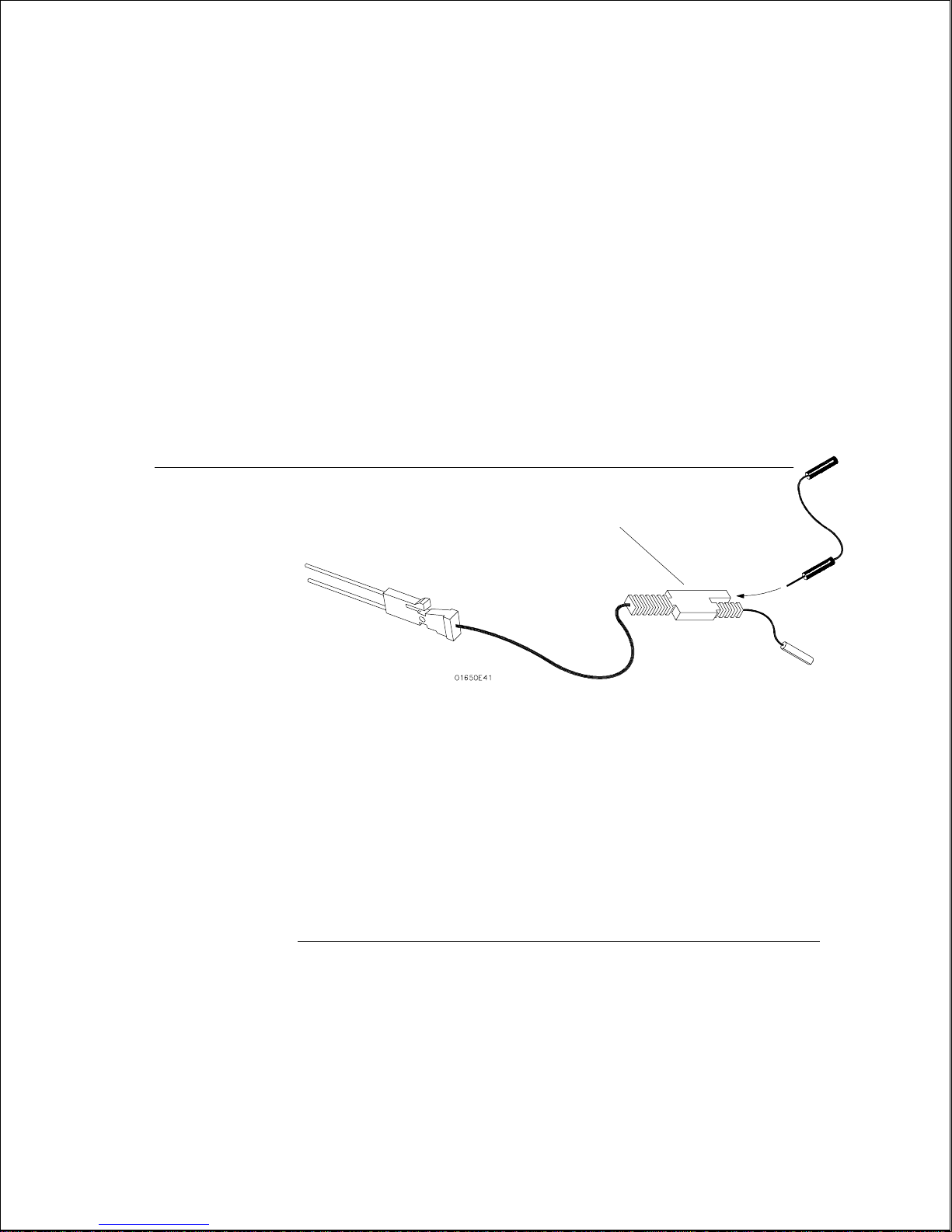
Probe Leads
The probe leads consists of a 12-inch twisted pair cable, a ground tap, and
one grabber. The probe lead, which connects to the target system, has an
integrated RC network with an input impedance of 100 kΩ in parallel with
approximately 8 pF, and all in series with 250 Ω.
The probe lead has a two-pin connector on one end that snaps into the probe
housing.
Probe lead connector
RC Network
Probe Lead
Grabbers
The grabbers have a small hook that fits around the IC pins and component
leads. The grabbers have been designed to fit on adjacent IC pins on either
through-hole or surface-mount components with lead spacing greater than or
equal to 0.050 in.
2–9
Page 26
CAUTION
WARNING
Probing
General Purpose Probing System Description
Probe Cable
The probe cable contains 18 signal lines, 17 chassis ground lines, and two
power lines for preprocessor use. The cables are woven together into a flat
ribbon that is 4.5 feet long. The probe cable connects the logic analyzer to
the pods, termination adapter, or preprocessor interface. Each cable is
capable of carrying 0.33 amps for preprocessor power.
DO NOT exceed this 0.33 amps per cable or the cable will be damaged.
Preprocessor power is protected by a current limiting circuit. If the current
limiting circuit is activated, the fault condition must be removed. After the
fault condition is removed, the circuit will reset in one minute.
Minimum Signal Amplitude
Any signal line you intend to probe with the logic analyzer probes must
supply a minimum voltage swing of 500 mV to the probe tip. If you measure
signal lines with a voltage swing of less than 500 mV, you may not obtain a
reliable measurement.
Maximum Probe Input Voltage
The maximum input voltage of each logic analyzer probe is ±40 volts peak,
CAT I.
Pod Thresholds
Logic analyzer pods have two preset thresholds and a user-definable pod
threshold. The two preset thresholds are ECL (− 1.3 V) and TTL (+1.5 V).
The user-definable threshold can be set anywhere between − 6.0 volts
and +6.0 volts in 0.05 volt increments.
All pod thresholds are set independently.
2–10
Page 27
Probing
Assembling the Probing System
Assembling the Probing System
The general-purpose probing system components are assembled as shown
below to make a connection between the measured signal line and the pods
displayed in the Format menu.
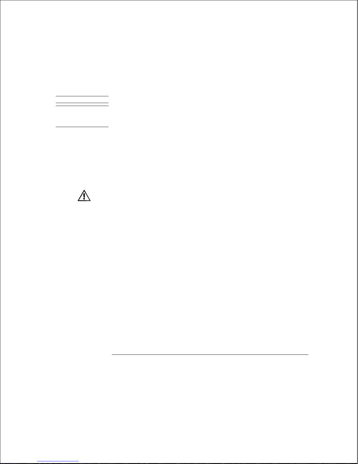
Connecting Probe Cables to the Logic Analyzer
2–11
Page 28
Probe tip assembly
Probe cable
Probing
Assembling the Probing System
Connecting Probe Cables to the Logic Analyzer
All probe cables are installed at Hewlett-Packard. If you need to replace a
probe cable, refer to the Service Guide, available from your HP Sales Office.
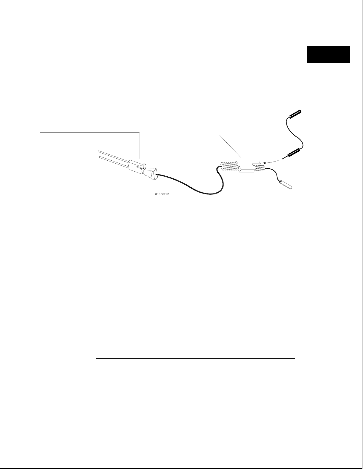
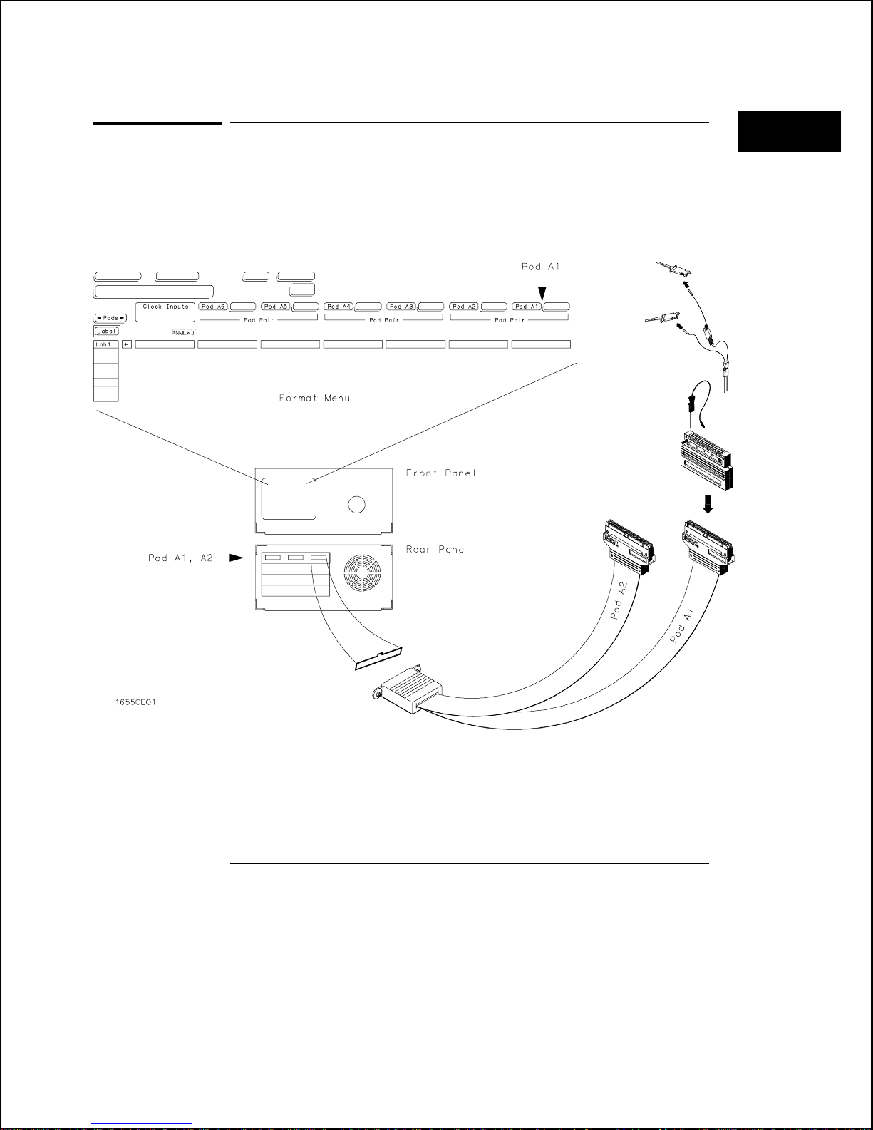
Connecting the Probe Tip Assembly to the Probe Cable
To connect a probe tip assembly to a cable, align the key on the cable
connector with the slot on the probe housing and press them together.
Connecting Probe Tip Assembly
2–12
Page 29
Probing
Assembling the Probing System
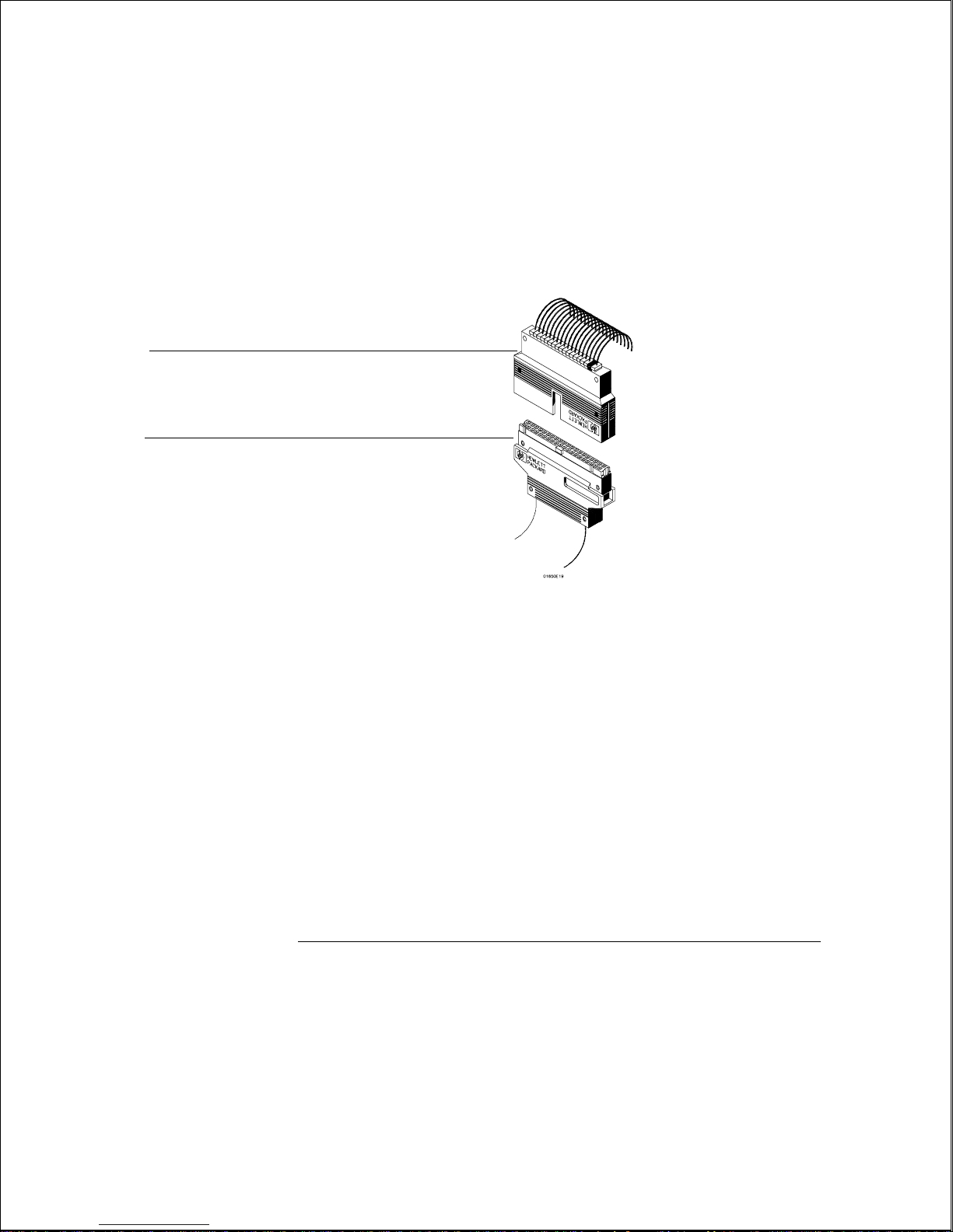
Disconnecting Probe Leads from Probe Tip Assemblies
When you receive the logic analyzer, the probe leads are already installed in
the probe tip assemblies. To keep unused probe leads out of your way during
a measurement, you can disconnect them from the pod.
To disconnect a probe, insert the tip of a ball-point pen into the latch
opening. Push on the latch while gently pulling the probe out of the pod
connector as shown in the figure below.
To connect the probes into the pods, insert the double pin end of the probe
into the probe housing. Both the double pin end of the probe and the probe
housing are keyed so they will fit together only one way.
Installing Probe Leads
2–13
Page 30
Probing
Assembling the Probing System
Connecting the Grabbers to the Probes
Connect the grabbers to the probe leads by slipping the connector at the end
of the probe onto the recessed pin located in the side of the grabber. If you
need to use grabbers for either the pod or the probe grounds, connect the
grabbers to the ground leads in the same manner.
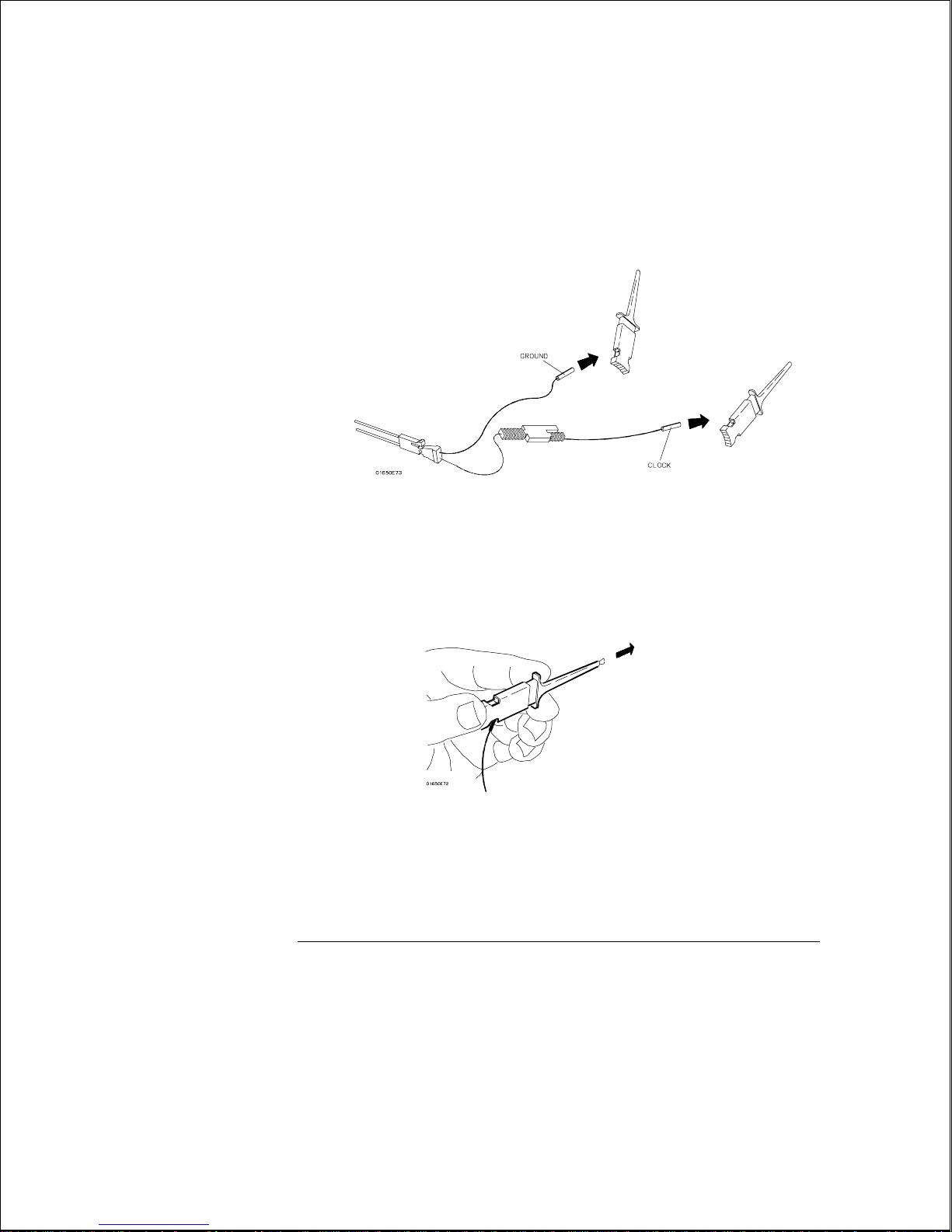
Connecting Grabbers to Probes
Connecting the Grabbers to the Test Points
The grabbers have a hook that fits around the IC pins and component leads.
Connect the grabber to the test point by pushing the rear of the grabber to
expose the hook. Hook the lead and release your thumb as shown below.
Connecting Grabbers to Test Points
2–14
Page 31

3
The Configuration Menu
Page 32

The Configuration Menu
The Configuration menu is one of the analyzer menus that allows you
to set module level parameters. For example, in the Configuration
menu the pod pair assignments are made. In addition, the type of
clocking is selected and a custom analyzer name can be assigned.
Configuration Menu Map
The following menu map illustrates all fields and the available options
in the Configuration menu. The menu map will help you get an
overview as well as provide you with a quick reference of what the
Configuration menu contains.
Configuration Menu Map
3–2
Page 33

The Configurat ion Menu
Name Field
Name Field
The Name field allows you to assign a specific name to the analyzer machine.
The name is entered by using the pop-up alpha-numeric keypad. When
configurations are stored to disk and later reloaded, a specific name can help
identify the measurement setup.
Name field
Keypad
Name Field
3–3
Page 34

The Configura tion Menu
Type Field
Type Field
The Type field allows you to configure the available analyzers as a state
analyzer or a timing analyzer. When the Type field is selected, the following
choices are available.
Timing
When Timing is selected, the analyzer uses its own internal clock to clock
measurement data into the acquisition memory. This clock is asynchronous
to the signals in the target system. When this option is selected, some fields
specific to external clocks will not appear in the analyzer menus.
The analyzer can only be configured with one timing analyzer. If two are
selected, the first will be turned off.
State
When State is selected, the data analyzer uses a clock from the system under
test to clock measurement data into acquisition memory. This clock is
synchronous to the signals in the target system.
Type field
Clock type selection menu
Type Field
3–4
Page 35

The Configurat ion Menu
Unassigned Pods List
Unassigned Pods List
The list of Unassigned Pods in the Configuration menu shows the available
pods for the module configuration. Pod grouping and assignment is by pod
pairs. When a pod pair is selected from the Unassigned Pods list, an
assignment menu appears. From the assignment menu, select a destination
for the pod pair.
Within each pod pair, activity indicators show the integrity of the connected
signals.
See Also For more information on the activity indicators, refer to "Activity Indicators"
found later in this chapter.
Unassigned pods listMachine assignment
Unassigned Po ds Display
3–5
Page 36

The Configura tion Menu
Unassigned Pods L ist
Illegal Configuration
When both analyzers are turned on, pod pair 1,2 and pod pair 5,6 cannot be
assigned to the same analyzer. If this configuration is set, the analyzer will
display a help menu. Use this help menu to reconfigure the pod assignment
to a legal configuration.
Pod Configuration Help Menu
3–6
Page 37

The Configurat ion Menu
Activity Indicators
Activity Indicators
A portion of the Configuration menu that is not a selectable field is the
Activity Indicators. The indicators appear in two places. One is in the pod
pair displays of this Configuration menu. The other place is in the bit
reference line in the Format menu just above the pod bit numbers.
When the logic analyzer is properly connected to an active target system, you
see either a high level dash, a low level dash, or a transitional arrow in the
Activity Indicator displays for each pod pair. These indicators are very useful
in showing proper probe connection and that the logic levels are as expected
according to the threshold level setting.
See Also The "Bit Assignment Fields" in the Format menu chapter for more
information on the activity indicators.
Activity indicato rs
Activity Indicators
3–7
Page 38

3–8
Page 39

4
The Format Menu
Page 40

The Format Menu
The Format menu is where you assign which data channels are
measured and what clocking arrangement is used to capture valid
data.
The configuration of the Format menu consists of grouping and
labeling the data channels from the system under test to fit your
particular measurement. In addition, for your convenience in
recognizing bit groupings, you can specify symbols to represents them.
If the analyzer is configured as a state analyzer, there are master and
slave clocks, clock qualifiers and a variable clock setup and hold to
further qualify what data is captured. In addition, you can set
individual pod clock threshold levels.
Format Menu Map
The following menu map graphically illustrates all fields in the Format
menu. Use the menu map as an overview and as a quick reference to
the available options in the Format menu.
4–2
Page 41

The Format Menu
The State Format Menu M ap
4–3
Page 42

The Format Menu
State Acquisition Mode Field (State only)
State Acquisition Mode Field (State only)
The State Acquisition Mode field identifies the channel width and memory
depth of the selected acquisition mode. When the State Acquisition Mode
field is selected, two configurations of channel width and memory depth
become available. Use the State Acquisition Mode to configure the analyzer
for the best use of available memory and channel width.
Full Channel 4K Memory 100MHz
The full channel selection uses both pods in a pod pair for 34 channels of
width and a total memory depth of 4096 samples per channel. If time or state
tags are turned on, the total memory could be split between data acquisition
storage and time or state tag storage. To maintain the full 4096 samples per
channel depth, leave one pod pair unassigned. State clock speed is 100 MHz.
Half Channel 8K Memory 100MHz
The half channel selection cuts the channel width to 17 channels. When in
this mode, the pod you use is selectable by selecting the Pod field, then
choosing one of the two pods within the pair. In Half Channel mode, the
memory depth is increased to 8192 samples per channel. Time or state tags
are not available in this mode. State clock speed is 100 MHz.
State acquisition
mode field
Acquisition mode
selection menu
Pod field
State Acquisition Mode Field
4–4
Page 43

The Format Menu
Timing Acquisition Mode Field (Timing only)
Timing Acquisition Mode Field (Timing only)
The Timing Acquisition Mode field displays the acquisition type, the channel
width, and sampling speed of the present acquisition mode. The Timing
Acquisition Mode field is used to access an acquisition mode selection menu.
Conventional Acquisition Mode
In Conventional Acquisition mode the analyzer stores measurement data at
each sampling interval.
Conventional Full Channel 250MHz The total memory depth is 4096
samples with data being sampled and stored as often as every 4 ns.
Conventional Half Channel 500MHz The total memory depth is 8192
samples with data being sampled and stored as often as every 2 ns.
Glitch Acquisition Mode
In Glitch Acquisition mode, a glitch is defined as a pulse with a minimum
width of 3.5 ns and a maximum width of 8 ns, or the sample period,
whichever is larger. As an example, if the sample period is 8 ns, then a glitch
is defined as being between 3.5 ns and 8 ns. One advantage of the glitch
mode is that if you expand the sample rate, a pulse that is less than the
sample rate will still be displayed as a vertical dashed line.
Glitch Half Channel 125MHz The total memory depth is split
between data storage and glitch storage. Data acquisition memory depth
is 2048 per channel. Glitch storage is 2048 per channel. Data is sampled
for new transitions every 8 ns.
Glitch in a Timing Waveform
4–5
Page 44

The Format Menu
Timing Acquisition Mode Field (Timing only)
Transitional Acquisition Mode
In Transitional Acquisition mode, the timing analyzer samples data at regular
intervals, but only stores data when there is a level transition on currently
assigned bits of a pod pair. Each time a level transition occurs on any of the
assigned bits, all bits of the pod pair are stored. A time tag is stored with
each stored data sample so the measurement can be reconstructed and
displayed later. If transitions are exceptionally far apart, the timer may
overflow. This does not generate a warning.
Difference in store d samples
Conventional and Transitional Comparison
One issue when using transitional timing is how many transitions can be
stored. The number depends on the mode and frequency of transition
occurrence. The following overview explains the number of transitions
stored for each transitional timing mode and why.
4–6
Page 45

The Format Menu
Timing Acquisition Mode Field (Timing only)
Transitional Full Channel 125 MHz Mode
The total memory depth is 4 Kbytes per channel with a channel width of 34
channels per pod pair. Data is sampled for new transitions every 8 ns.
When the Timing analyzer runs in the 125 MHz mode, it operates very similar
to the state analyzer with count Time turned on. The only exceptions are
that the store qualification comes from transition detectors instead of the
sequencer. Also, the analyzer uses an internal clock.
With 4 Kbytes of memory per channel and count Time turned on, the
analyzer uses half its memory (2 Kbytes) to store time tags. It should be
noted that each pod pair must store transitions at its own rate, therefore it
must store its own set of time-tags. You do not have the option of using a
free pod to retain full memory as you have in the normal state mode.
When a transition is detected after a sample with no detected transition,
two samples are stored. One sample is a "before transition sample" and the
other is an "after transition sample." Then, as long as there are transitions in
the subsequent sample, only 1 sample is stored. When the next sample
occurs without a transition, the two stored sample sequence (one before, one
after) repeats with the next detected transition.
4–7
Page 46

The Format Menu
Timing Acquisition Mode Field (Timing only)
Minimum Transitions Stored Normally, transitions occur at a
relatively slow rate, a rate slow enough to ensure at least one sample
with no transitions between the samples with transitions. This is
illustrated below with time-tags 2, 5, 7, and 14. When transitions happen
at this rate, two cycles are stored for every transition. This means that
with 2 Kbytes of memory, 1 Kbyte of transitions is stored. You must
subtract 1, which is necessary for a starting point, for a minimum of 1023
stored transitions.
Maximum Transitions Stored If transitions occur at a fast rate, such
that there is a transition at each sample point, only one sample is stored
for each transition as shown by time-tags 17 through 21 below. If this
continues for the entire trace, the number of transitions stored is
2 Kbytes. Again, you must subtract the starting point sample which then
yields a maximum of 2047 stored transitions.
In most cases a transitional timing trace is stored by a mixture of the
minimum and maximum cases. Therefore, the actual number of transitions
stored will be between 1023 and 2047.
Storing Time-tags and Transitions
4–8
Page 47

The Format Menu
Timing Acquisition Mode Field (Timing only)
Transitional Half Channel 250 MHz Mode
The total memory depth is 8 Kbytes with a channel width of 17 channels on
one pod. The pod used within the pod pair is selectable. Data is sampled for
new transitions every 4 ns.
Transitional timing running at 250 MHz is the same as the 125 MHz mode,
except that two single-pod data samples (17 bits x 2 = 34 bits) are stored
instead of one full-pod pair data sample (34 bits). This is because in half
channel mode, data is multiplexed into the sequencer pipeline in two 17-bit
samples. The first 17 bit sample is latched, the next 17-bit sample is sent
down the pipeline along with the latched 17-bit sample.
This operation keeps the pipeline frequency down to 125 MHz. It should be
noted that the transition detector still looks at a full 34 bits. This means it is
looking at two samples at a time instead of one. In this mode, between 682
and 4094 transitions are stored.
Minimum Transitions Stored The following example shows what data
is stored from a data stream with transitions that occur at a slow rate
(more than 24 ns apart).
Minimum Transitions Stored
4–9
Page 48

The Format Menu
Timing Acquisition Mode Field (Timing only)
As you can see, transitions are stored in two different ways, depending
strictly on chance. Remember that the transition detector only looks at the
full 34 bits while the data is stored as two 17-bit samples. So, the transition
detector will not see time-tag 3 (101/000) as a transition. However, when it
compares it to time-tags 2 (101/101) or 4 (000/000), it sees a difference and
detects them as transitions. For this first set of time-tags, the transition
detector sees more transitions than are really there. This causes the analyzer
to store 6 samples per transition (three 34-bit sample pairs), instead of just
two, as in the 125-MHz mode. If all the transitions will be stored in this way
throughout the trace, the minimum number of stored transitions are 682
(4096/6).
However, as you see with time-tags 7 (000/000) and 8 (001/001), transitions
can fall between the pairs of samples. When this happens, only one transition
is detected and only 4 samples (two sample pairs) are stored. If all
transitions will be stored in this way, 1023 (4096/4) transitions are stored.
From run to run, the actual number of transitions stored for transitions that
occur at a slower rate will fall between these two numbers, based on the
probability of a transition falling between a sample pair or falling within a
sample pair.
Maximum Transitions Stored The following example shows the case
where the transitions are occurring at a 4 ns rate:
Maximum Transitions Stored
4–10
Page 49

The Format Menu
Timing Acquisition Mode Field (Timing only)
In this case, transitions are being detected with each sample. Therefore,
they are all being stored. In addition, each sample pair contains a transition.
For example, time tag 1 (100/000) contains a transition and is different from
time tag 2 (111/011), which also contains a transition. The difference
between the two will trigger the transition detector.
If this were to continue throughout the trace, You would store 4 Kbytes −1
transitions, or 4095. As with the 125-MHz mode, the actual number of
transitions stored will fall somewhere between 682 and 4095, depending on
the frequency of transitions.
Other Transitional Timing Considerations
Pod Pairs are Independent In single run mode each pod pair runs
independently. This means when one pod pair fills its trace buffer it will
not shut the others down. Should you have a pod pair with enabled data
lines and with no transitions on its lines, you get a message "Storing
transitions after trigger for pods nn/nn." In repetitive run mode, a full
pod pair waits 2 seconds, then halts all other pod pairs.
4–11
Page 50

The Format Menu
Timing Acquisition Mode Field (Timing only)
Increasing Duration of Storage In the 125-MHz mode a transition on
any one of the 34 bits each sample (if they are all turned on) will cause
storage. Reducing the number of bits that are turned on for any one pod
pair will more than likely increase data storage time.
Separating data lines which contain fast occurring transitions from lines with
slow occurring transitions also helps. When doing this, be sure to cross pod
pair boundaries. It does not help to move fast lines from pod 1 to pod 2, they
must be moved to pod 3, which is a different pod pair.
In the 250 MHz mode a transition on any one of 17 bits (half channel) each
sample (if they are all turned on) will cause storage.
Invalid Data The analyzer only looks for transitions on data lines that
are turned on. Data lines that are turned off store data, but only when
one of the lines that is turned on transitions. If the data line is turned on
after a run, you would see data, but it is unlikely that every transition
that occurred was captured.
4–12
Page 51

The Format Menu
Clock Inputs Display
Clock Inputs Display
Beneath the Clock Inputs display, and next to the bit reference line, is a
display of all clock inputs available in the present configuration. In a one card
module the J and K clocks appears with pod pair 1/2, the L and M with pod
pair 3/4, and clocks N and P with pod pairs 5/6. In a two card module the
next six clocks appear to the left of the displayed master clocks, and are used
as data channels. With the exception of the Range resource, all unused clock
bits can be used as data channels. If any clock line is used as a data channel,
the bit must be assigned. Activity indicators above the clock identifier show
clock or data signal activity.
Clock inputs display
Clock Inputs Display
Clocks assigned
as data channels
4–13
Page 52

The Format Menu
Pod Field
Pod Field
The Pod field identifies which pod of a pod pair the settings of the bit
assignment field, pod threshold field, and pod clock fields effect. In the full
channel modes, this field is simply an identifier and is not selectable.
However, in the half channel mode, the Pod field turns dark which means it is
selectable. In the half channel mode, one pod of a pod pair is selectable and
all pod settings effect the selected pod.
Pod field
Pod Field
4–14
Page 53

The Format Menu
Pod Clock Field (State only)
Pod Clock Field (State only)
The Pod Clock field identifies the type of clock arrangement assigned to each
pod. When the Pod Clock field is selected, a clock arrangement type menu
appears with the choices of Master, Slave, or Demultiplex. Once a pod clock
is assigned a clock arrangement, its identity and function follows what is
configured in the Master and Slave Clock fields. The Pod Clock field and the
clocking arrangement is only available in a state analyzer.
Master
This option specifies that data on all pods designated "Master Clock", in the
same analyzer, are strobed into memory when the status of the clock lines
match the clocking arrangement specified under the Master Clock.
See Also The "Master and Slave Clock Field" found later in this chapter for information
about configuring a clocking arrangement.
The "Type Field" in the Configuration menu chapter for information on
selecting analyzer types.
Pod clock field
Arrangement type selection menu
Pod Clock Field
4–15
Page 54

The Format Menu
Pod Clock Field (State only)
Slave
This option specifies that data on a pod designated "Slave Clock", are latched
when the status of the slave clock inputs meet the requirements of the slave
clocking arrangement. Then, followed by a match of the master clock and
the master clock arrangement, the slave data is strobed into analyzer memory
along with the master data. See the figure below.
If multiple slave clocks occur between master clocks, only the data latched by
the last slave clock prior to the master clock is strobed into analyzer memory.
Analyzer Memory
Latching Slave Data
Pod 2
Master
Slave clock arrangement field
Slave Latch
Pod 1
Slave
Master
Clock
Slave
Clock
Slave Clock Field
4–16
Page 55

Demultiplex mode field
The Format Menu
Pod Clock Field (State only)
Demultiplex
The Demultiplex mode is used to store two different sets of data that occur at
different times on the same channels. In Demultiplex mode, only one pod of
the pod pair is used, and that pod is selectable. Both the master and slave
clocks are used in the Demultiplex mode. Channels assignments are
displayed as Demux Master and Demux Slave. For easy recognition of the
two sets of data assign slave and master data to separate labels.
Demultiplex Cl ocking Mode
4–17
Page 56

The Format Menu
Pod Clock Field (State only)
When the analyzer sees a match between the slave clock input and the Slave
Clock arrangement, Demux Slave data is latched. Then, followed by a match
of the master clock and the master clock arrangement, the slave data is
strobed into analyzer memory along with the master data. If multiple slave
clocks occur between master clocks, only the data latched by the last slave
clock prior to the master clock is strobed into analyzer memory.
Analyzer Memory
Pod 1
Latching Slave Data In Demultiplex Mode
Slave Latch
Pod 2 is not connected
Master
Clock
Slave
Clock
4–18
Page 57

The Format Menu
Pod Threshold Field
Pod Threshold Field
The pod threshold field is used to set a voltage level which the data must
reach before the analyzer recognizes and displays it as a change in logic
levels. You specify a threshold level for each pod in a pod pair. The level
specified for each pod is also assigned to the pods clock threshold.
When the Pod Threshold field is touched, a threshold selection pop-up
appears with the following choices:
TTL
When TTL is selected as the threshold level, the data signals must reach +1.5
volts.
ECL
When ECL is selected as the threshold level, the data signals must reach −1.3
volts.
USER
When User is selected as the threshold level, the data signals must reach a
user-selectable value between −6.0 volts to +6.0 volts.
Pod Threshold Field
Pod threshold field
Pod Threshold
selection me nu
4–19
Page 58

The Format Menu
Master and Slave Clock Field (State only)
Master and Slave Clock Field (State only)
The Master and Slave Clock fields are used to construct a clocking
arrangement. A clocking arrangement is the assignment of appropriate
clocks, clock edges, and clock qualifier levels which allow the analyzer to
synchronize itself on valid data.
Clock Selections
When the Master or Slave Clock field is selected, a clock/qualifier selection
menu appears showing the available clocks and qualifiers for a clocking
arrangement. There are up to six clocks available (J through P), and four
clock qualifiers available (Q1 through Q4).
Each pod cable has one clock line and at least one clock edge must be
assigned for all pods in a state analyzer. If a second analyzer card is
connected, the lower card in the frame becomes the master and only its six
clocks can be assigned as clocks. The remaining unassigned clocks can be
used as data channels.
See Also The "Pod Clock Field" found earlier in this chapter for information on
selecting clocking arrangement types such as Master, Slave, or Demultiplex.
Master clock field
Master Clock Field
4–20
Page 59

Clock edge
selection me nu
The Format Menu
Master and Slave Clock Field (State only)
All combinations of the J, K, and L clock and Q1 and Q2 qualifiers are ORed
to the clock combinations of the M, N, and P clocks and Q3 and Q4 qualifiers.
Clock edges are ORed to clock edges, clock qualifier are ANDed to clock
edges, and clock qualifiers can be either ANDed or ORed together.
The clock threshold level is the same as the level assigned in the Pod
Threshold field.
Clock Edges and Levels
4–21
Page 60

The Format Menu
Setup/Hold Field (State only)
Setup/Hold Field (State only)
Setup/Hold adjusts the relative position of the clock edge with respect to the
time period that data is valid. When the Setup/Hold field is selected, a
configuration menu appears. Use this Setup/Hold configuration menu to
select each pod in the analyzer and assign a Setup/Hold selection from the
selection list.
With a single clock edge assigned, the choices range from 3.5 ns Setup/0.0 ns
Hold, to 0.0 ns Setup/3.5 ns Hold. With both edges of a single clock assigned,
the choices are from 4.0 ns Setup/0.0 ns Hold, to 0.0 ns Setup/4.0 ns Hold. If
the analyzer has multiple clock edges assigned, the choices range from 4.5 ns
Setup/0.0 ns Hold, to 0.0 ns Setup/4.5 ns Hold.
Setup and hold menu
Setup / Hold field
Setup and Hold Menu
4–22
Page 61

The Format Menu
Setup/Hold Field (State only)
The relationship of the clock signal and valid data under the default setup
and hold is shown in the figure below.
Default Setup and Hold
If the relationship of the clock signal and valid data is such that the data is
valid for 1 ns before the clock occurs and 3 ns after the clock occurs, you will
want to use the 1.0 setup and 2.5 hold setting.
Clock Position in Valid Data
4–23
Page 62

The Format Menu
Symbols Field
Symbols Field
See Also Refer to Symbols Assignment in the "Common Module Operations" part of the
HP 16500B User’s Reference or HP 16500C User’s Reference for complete
information on using symbols.
Label Assignment Fields
See Also Refer to Labels Assignment in the "Common Module Operations" part of the
HP 16500B User’s Reference or HP 16500C User’s Reference for complete
information on using labels.
Rolling Labels and Pods
See Also The rolling function is the same for all items that are stored offscreen. For
more information on rolling labels and pods, refer to Labels Assignment in
the "Common Module Operations" part of the HP 16500B User’s Reference
or HP 16500C User’s Reference for complete information.
4–24
Page 63

The Format Menu
Label Polarity Fields
Label Polarity Fields
The Label Polarity fields are used to assign a polarity to each label. The
default polarity for all labels is positive ( + ). You change the label polarity by
touching the polarity field, which toggles the polarity between positive
( + ) and negative ( −).
When the polarity is inverted, all data as well as bit pattern specific
configurations used for identifying, triggering, or storing data reflect the
change of polarity.
In a timing analyzer with the data inverted, the waveform display does not
change.
Polarity field
Polarity Field
4–25
Page 64

The Format Menu
Bit Assignment Fields
Bit Assignment Fields
The bit assignment fields are used to assign bits (channels) to labels. The
convention for bit assignment is as follows:
* (asterisk) indicates assigned bit.
. (period) indicates unassigned bit.
To change a bit assignment, select the bit assignment field and using the
knob, move the cursor to the bit you want to change, then select an asterisk
or a period. When the bits are assigned as desired, and you close the pop-up,
the screen displays the new bit assignment.
Above each column of bit assignment fields is a bit reference line that tells
you the bit numbers from 0 to 15, with the left bit numbered 15 and the right
bit numbered 0. This bit reference line helps you know exactly which bits
you have assigned by displaying activity indicators when a proper connection
from the probe is recognized.
See Also The "Activity Indicators" in the Configuration menu chapter for more
information on the bit reference line and the activity indicators on the bit
reference line.
Bit Assignment Field
4–26
Bit assignment field
Page 65

The Format Menu
Bit Assignment Fields
Labels may have from 1 to 32 channels assigned to them. If you try to assign
more than 32 channels to a label, the logic analyzer will beep, indicating an
error, and a message will appear at the top of the screen telling you that 32
channels per label is the maximum.
Channels assigned to a label are numbered from right to left by the logic
analyzer. The least significant assigned bit on the far right is numbered 0, the
next assigned bit is numbered 1, and so on. Since 32 channels can be
assigned to one label at most, the highest number that can be given to a
channel is 31.
Although labels can contain split fields, assigned channels are always
numbered consecutively within a label.
Bit Assignment Example
4–27
Page 66

4–28
Page 67

5
The Trigger Menu
Page 68

The Trigger Menu
The Trigger menu is used to configure when the analyzer triggers,
what the analyzer triggers on, and what is stored in acquisition
memory. In addition, within the Acquisition Control function,
prestore and poststore requirements are set. The Trigger menu is
divided into three areas, each dealing with a different area of general
operation.
• Sequence Levels
• Resource Terms
• Acquisition Control
Sequence levels area
Resource ter ms area
Acquisition co ntrol area
Trigger Menu Areas
5–2
Page 69

The Trigger M enu
Sequence Levels Area
You use the sequence levels area to view the sequence levels currently
used in the trigger specification and their timer status. From this area
you can also access each individual level for editing.
Resource Terms Area
You use the resource terms area to assign values to the resource
terms. Resource terms take the form of bit patterns, ranges, and
edges. In addition to assigning values to the resource terms, you also
assign values to the two timers, and assign custom names to all the
resource terms.
Once defined and inserted into the trigger specification, the resource
terms will identify key points in the data stream for branching or the
point for data acquisition to occur.
Control Area
You use the acquisition control area to manage the efficient use of
analyzer memory. You define any arming control or whether you want
time or count tags placed in the stored data.
Within the Acquisition Control function, you can adjust trigger
position, sample period, memory length, and whether the resource
term that generated a branch is stored.
Trigger Menu Map
The following menu map illustrates all fields and available options in
the Trigger menu. The menu map will give you an overview as well as
provide you with a quick reference of what the Trigger menu contains.
5–3
Page 70

The Trigger M enu
Trigger Menu Map
5–4
Page 71

The Trigger M enu
Trigger Menu Map (Continued)
5–5
Page 72

Trigger Sequence Levels
Sequence levels are the definable stages of the total trigger
specification. When defined, sequence levels control what the
analyzer triggers on, when the analyzer triggers, and where trigger will
be located in the total block of acquired data. In addition, you can
qualify what data is stored when trigger occurs.
By using sequence levels, you create a sequence of instructions for
the analyzer to follow. As the sequence levels are executed, all
subsequent branching and sequence flow is directed by the
statements within the sequence levels. The path taken resembles a
flow chart, and the end result is the desired trigger point.
Individual sequence levels are assigned either a pre-defined trigger
macro, or a User-level trigger macro. The total trigger specification,
(one or more sequence levels) can contain pre-defined macros,
User-level macros, or a combination of both. You finish defining each
level by inserting resource terms, timers, or occurrence counters into
assignment fields within each macro.
In State Acquisition Mode, there are 12 sequence levels available. In
Timing Acquisition Mode there are 10 sequence levels available.
Sequence Level Usage
Generally, you would think using one macro in one sequence level
uses up one of the available sequence levels. This may not always be
the case. Some of the more complex pre-defined macros require
multiple sequence levels. Keep this point in mind if you are near the
limit on remaining sequence levels. The exact number of internal
levels required per macro, and the remaining available levels, is shown
within the macro library list.
The only instance where multiple levels are used with the User-level
macro, is when the "<" duration is assigned.
5–6
Page 73

Sequence level number
The Trigger M enu
Editing Sequence Levels
The higher level editing, such as adding or deleting entire sequence
levels, is done using the Modify Trigger field in the main Trigger
menu. You can also modify any existing sequence level from the
Modify Trigger field.
Another way of editing a specific sequence level is to select the
sequence level number field. If the number field in offscreen, select
the sequence levels roll field turning it light blue, then use the knob to
roll the level back onscreen.
Sequence level roll field
Modify trigger
Accessing Sequence Levels
Once you are in any sequence level, you can reconfigure the existing
macro by selecting and reassigning the assignment fields and value
fields. All appropriate resource terms appear in pop-up selection lists
after any of the assignment fields are selected.
To edit the actual values assigned to the resource terms, exit the
sequence level and make changes to the terms assignment fields in
the resource terms area.
See Also "Assigning Resource Term Names and Values" found later in this chapter.
5–7
Page 74

The Trigger M enu
Modify Trigger Field
Modify Trigger Field
The Modify Trigger field allows you to modify the statements of any single
sequence level as well as other high level actions like global clearing of
existing trigger statements, and adding or deleting sequence levels.
Modify Modify Sequence Level
Replace Sequence Level
Delete Sequence Level
Add Sequence Level
Clear Trigger
Break Down Macro
Cancel
Modify Sequence Level
If there is more than one sequence level assigned, you are asked which level
to modify. Once in the desired sequence level, make all appropriate resource
changes, then select Done.
Replace Sequence Level
If there is more than one sequence level assigned, you are asked which level
to replace. When you replace a level, you pick a new macro to replace the
old one. You then assign the appropriate resource in the new level.
5–8
Page 75

The Trigger M enu
Modify Trigger Field
Delete Sequence Level
If there is more than one sequence level assigned, you are asked which level
to delete.
Add Sequence Level
By default you have one sequence level available at powerup. When you add
sequence levels, you are given the choice of inserting them before or after a
sequence level.
Clear Trigger
The Clear Trigger field accesses a selection menu used to clear any
user-defined values within the trigger specification or within the resource
terms list.
Clear All The Clear All option clears sequence levels, resource terms,
and resource term names back to their default values.
Clear Sequence Levels The Clear Sequence Levels option resets all
assignment fields in the sequence levels to their default values. Any
custom names assigned to the resource terms will remain.
Clear Resource Terms The Clear Resources Terms option will reset
all assignment fields for the resource terms back to their default values.
Clear Resource Term Names The Clear Resource Term Names option
resets all custom names assigned to the resource terms back their default
values.
5–9
Page 76

The Trigger M enu
Modify Trigger Field
Break Down Macros / Restore Macros
When a pre-defined macro is broken down, the contents of that macro are
displayed in the same long form used in the User-level macro. If the macro
uses multiple internal levels, all levels are separated out and displayed in the
sequence level area of the Trigger menu. Once the macros in your trigger
specification are broken down, the Break Down Macros field changes to
Restore Macros. Use the Restore Macros field to restore all macros to their
original structure.
While in a broken down form, you can change the structure. However, when
the macros are restored, all changes are lost and any branching that is part of
the original structure is restored.
Use the Break Down Macros if you want to view a particular macro part in its
long form to see exactly what flow the sequencer is following. It can also be
used as an aid in creating a custom trigger specification. In this application,
you would start with a pre-defined macro, break it down, then customize the
long form to meet your needs.
When a macro is broken down, you have all the assignment fields and
branching options available as if you have configured a User-level macro. For
information on the assignment fields, branching, occurrence counters, and
time duration function, refer to the section, "Modifying the User-level Macro"
found later in this chapter.
5–10
Page 77

Pre-defined Trigger Macros
Both the state and timing acquisition modes have a macro library
containing pre-defined trigger macros. Depending on which
acquisition mode you are using, you get the corresponding library.
Each macro will require at least one sequence level, and in some
cases, may require multiple levels. Sequence levels containing
pre-defined macros flow linear without branching. However, if
branching is required, the User-level macro can be inserted to provide
a branch.
Both lists of macros are divided into the following different groups
depending on their function.
Timing Trigger Macro Library:
• User Mode (User-level macro)
• Basic Macros
• Pattern/Edge Combination Macros
• Time Violation Macros
• Delay Macros
Timing Trigger Macro Library
5–11
Page 78

The Trigger M enu
Modify Trigger Field
State Trigger Macro Library:
• User Mode (User-level macro)
• Basic Macros
• Sequence Dependent Macros
• Time Violation Macros
• Delay Macros
State Trigger Macro Library
5–12
Page 79

The Trigger M enu
Using Macros to Create a Trigger Specification
Using Macros to Create a Trigger Specification
To configure a trigger specification using trigger macros, follow the
procedure below.
From the Trigger menu, enter the desired sequence level through the
1
Modify Trigger field, or by selecting a sequence level number.
See Also "Editing Sequence Levels" and "Modify Trigger Field" found earlier in this
chapter for information on accessing levels.
From within the sequence level, select the Select New Macro field.
2
Select New Macro field
Assignment field
Select New Macro Field
3 Scroll and highlight the macro you want, then select the Select field.
4 Select the appropriate assignment fields and insert the desired
pre-defined resource terms, numeric values, and other parameter
fields required by the macro. Select the
In State Acquisition mode, a "Store" sequence level is always the last level.
This level is placed at the end of the trigger specification automatically.
See Also "Resource Terms" found later in this chapter for information on using
pre-defined resource terms.
Done field.
5–13
Page 80

The Trigger M enu
Timing Trigger Macro Library
Timing Trigger Macro Library
The following list contains all the macros in the Timing Trigger Macro
Library. They are listed in the same order as they appear onscreen.
User Mode User level - custom combinations, branching
The User level is a user-definable level. This level offers low level
configuration and uses one internal sequence level. If the "<" duration is
used, four levels are required.
Basic Macros 1. Find anystate "n" times
This macro becomes true when it sees any state occuring "n" number of
times. It uses one internal sequence level.
2. Find pattern present/absent for > duration
This macro becomes true when it finds a designated pattern that has been
present or absent for greater than or equal to the set duration. It uses one
internal sequence level.
3. Find pattern present/absent for < duration
This macro becomes true when it finds a designated pattern that has been
present or absent for less than the set duration. It uses four internal
sequence levels.
4. Find edge
This macro becomes true when the designated edge is seen. It uses one
internal sequence level.
5. Find Nth occurrence of an edge
This macro becomes true when it finds the "n" th occurrence of a designated
edge. It uses one internal sequence level.
5–14
Page 81

The Trigger M enu
Timing Trigger Macro Library
Pattern/Edge
1. Find edge within a valid pattern.
Combinations
This macro becomes true when a selected edge type is seen within the time
window defined by a designated pattern. It uses two internal sequence levels.
2. Find pattern occurring too soon after edge
This macro becomes true when a designated pattern is seen occurring within
a set duration after a selected edge type is seen. It uses three internal
sequence levels.
3. Find pattern occurring too late after edge
This macro becomes true when one selected edge type occurs, and for a
designated period of time after that first edge is seen, a pattern is not seen.
It uses two internal sequence levels.
Time Violations 1. Find two edges too close together
This macro becomes true when a second selected edge is seen occurring
within a designated period of time after the occurrence of a first selected
edge. It uses three internal sequence levels.
2. Find two edges too far apart
This macro becomes true when a second selected edge occurs beyond a
designated period of time after the first selected edge. It uses two internal
sequence levels.
3. Find width violation on a pattern/pulse
This macro becomes true when the width of a pattern violates designated
minimum and maximum width settings. It uses four internal sequence levels.
Delay 1. Wait "t" seconds
This macro becomes true after a designated time period has expired. It uses
one internal sequence level.
5–15
Page 82

The Trigger M enu
State Trigger Macro Library
State Trigger Macro Library
The following list contains all the macros in the State Trigger Macro Library.
They are listed in the same order as they appear onscreen.
User Mode User level - custom combinations, loops
The User level is a user-definable level. This level offers low level
configuration and uses one internal sequence level.
Basic Macros 1. Find anystate "n" times
This macro becomes true when the first state it sees occurs "n" number of
times. It uses one internal sequence level.
2. Find event "n" times
This macro becomes true when it sees a designated pattern occurring a
designated number of times consecutively or nonconsecutively. It uses one
internal sequence level.
3. Find event "n" consecutive times
This macro becomes true when it sees a designated pattern occurring a
designated number of consecutive times. It uses one internal sequence level.
4. Find event 2 immediately after event 1
This macro becomes true when the first designated pattern is seen
immediately followed by a second designated pattern. It uses two internal
sequence levels.
5–16
Page 83

The Trigger M enu
State Trigg er Macro Library
Sequence
Dependent macros
1. Find event 2 "n" times after event 1, before event 3 occurs
This macro becomes true when it first finds a designated pattern 1, followed
by a selected number of occurrences of a designated pattern 2. In addition, if
a designated pattern 3 is seen anytime while the sequence is not yet true, the
sequence starts over. If patt2’s "nth" occurrence is coincident with patt3,
patt2 takes precedence. It uses two internal sequence levels.
2. Find too few states between event 1 and event 2.
This macro becomes true when a designated pattern 1 is seen, followed by a
designated pattern 2, and with less than a selected number of states
occurring between the two patterns. It uses three internal sequence levels.
3. Find too many states between event 1 and event 2.
This macro becomes true when a designated pattern 1 is seen, followed by at
least a selected number of states, then followed by a designated pattern 2. It
uses two internal sequence levels.
4. Find n-bit serial pattern
This macro finds an "n" bit serial pattern on a given channel for a given label.
5–17
Page 84

The Trigger M enu
State Trigger Macro Library
Time Violations 1. Find event 2 occurring too soon after event 1
This macro becomes true when a designated pattern 1 is seen, followed by a
designated pattern 2, and with less than a selected time period occurring
between the two patterns. It uses two internal sequence levels..
2. Find event 2 occurring too late after event 1
This macro becomes true when a designated pattern 1 is seen, followed by at
least a selected time period, before a designated pattern 2 occurs. It uses
two internal sequence levels.
Delay 1. Wait "n" external clock states
This macro becomes true after a designated number of user clock states have
occurred. It uses one internal sequence level.
5–18
Page 85

The Trigger M enu
Modifying the User-level Macro
Modifying the User-level Macro
Before you begin building a trigger specification using the User-level macro,
it should be noted that in most cases one of the pre-defined trigger macros
will work.
If you need to accommodate a specific trigger condition, or you prefer to
construct a trigger specification from scratch, you will use the User-level
macro to build from. This macro appears in long form, which means it has
the analyzer’s total flexibility available in terms of resource terms, global
timers, occurrence counters, duration counters, and two-way branching.
The User-level macro has a "fill-in-the-blanks" type statement. You have the
following elements to use:
Bit Patterns, Ranges, and Edges
•
Storage Qualification
•
< and > Durations
•
Occurrence Counters
•
Timers
•
Branching
•
Primary "Find" branch
Secondary "else on"
branch
Assignment field
User-level Macro
5–19
Page 86

The Trigger M enu
Modifying the User-level Macro
The number of User-level macros you will use, or what you assign to the
resource terms is difficult to predict because of the variety of applications. A
general approach is to think of each field assignment or each new sequence
level as an opportunity to lead the analyzer through key points in the data
stream. Your end result is to select the desired point in the data to trigger
on, and to store only the data you want. If you know the data structure and
flow well enough, you could build a flowchart.
A typical method used during a debug operation is to first trigger on a known
pattern, edge or range. From that point, it becomes an iterative process of
adding more levels to further filter the data. It is important for you to know
how to use such elements as occurrence counters, timers, and branching, to
zero in and trigger at the desired point.
As the analyzer executes the trigger specification, it searches for a match
between the resource term value and the data. When a match is found, that
part of the sequence statement becomes true and the sequencing continues
to the next part of the statement or the next sequence level.
Eventually a path of "true" resource terms leads to your trigger command. If
timers or occurrence counters are used, the analyzer waits or counts
occurrences of a specified value before continuing.
The following examples illustrate the use of resource terms, occurrence
counters, timers, branching, and store qualification. You will use them in
your trigger specification either by themselves or in combination with each
other.
Using Bit Patterns, Ranges, and Edges
Bit patterns are set to match specific data values, and ranges are set to match
a range of bit patterns. In the Timing Acquisition mode, edges are set to
match specific edges of a timing pulse.
Example The following statement looks for the bit pattern you assigned to term "a" to
occur "1" time, before it triggers.
5–20
Page 87

The Trigger M enu
Modifying the User-level Macro
Example The following statement looks for the positive, negative, or either going edge
type you assigned to term "Edge1" to occur "1" time, before it Triggers .
Example The following statement looks for the combination of either a bit pattern you
assigned to "a" or an edge type you assigned to "Edge1" to occur "1" time
before it Triggers.
Example The following statement looks for a range of bit patterns assigned to "Range1"
to occur "2" times before it branches to the next sequence level.
See Also "Assigning Resource Term Names and Values" for more information on using
resource terms by themselves and in combinations.
5–21
Page 88

The Trigger M enu
Modifying the User-level Macro
Using Storage Qualification
Store qualification enables you to store all data, no data, or just selected data,
before trigger occurs.
Example The following statement determines that all occurrences of the bit pattern
you assigned to "a" will be stored before trigger occurs.
Setting < and > Durations (Timing only)
When a resource term is found during a timing sequence evaluation, you can
dictate how long the term must remain before the term actually becomes
true. When < or > duration is assigned, the secondary branching (Else on) is
not available.
Example The following statement dictates the bit pattern you assigned to "a" must
appear and remain present for greater than 8 ns.
> Field When greater-than (>) is used, the analyzer continues sequence
level evaluation only after the resource term has been true for greater
than or equal to the amount of duration specified.
< Field When less-than (<) is used, the analyzer continues sequence
level evaluation only after the resource term has been true for less than
or equal to the amount of duration specified. For each (<) assignment,
you must delete 4 levels from the total number of sequence levels. So in
actuality, using a less than sign requires four sequence levels.
5–22
Page 89

The Trigger M enu
Modifying the User-level Macro
Using the Occurrence Counters
Occurs Field When "Occurs" is selected, the < and > duration functions
change to an occurrence counter. Use the occurrence counter to delay
sequence evaluation until the resource term has occurred a designated
number times. If the "else on" branch becomes true before all specified
occurrences of the primary "Trigger on" branch, the secondary "else on"
branch is taken.
Example The following statement assigns the Occurrence Counter to the primary
"Trigger on" branch. Once the Occurrence Counter is assigned, a new
assignment field appears to set the number of occurrences.
5–23
Page 90

The Trigger M enu
Modifying the User-level Macro
Using the Timer
Timers are like other resource terms in that they are either true or false.
Timers can be set to Start, Stop, Pause, or Continue as the analyzer enters a
sequence level. The two timers are global, so each sequence level has the
ability to control the same timer. The default timer condition in all sequence
levels is Off.
Example The following statement assigns the "Timer 1" to the secondary "else on"
branch. If the bit pattern is not seen before the timer counts 400ns, the
secondary branch is taken to level 2.
See Also The "Timer Terms" found later in this chapter for information on how timers
work and how to assign a value to a timer.
5–24
Page 91

The Trigger M enu
Modifying the User-level Macro
Branching
If either the < or > durations is used, only the primary "Trigger on" branch is
available, otherwise each sequence level has two way branching.
If the primary branch is taken, the analyzer triggers and goes to the next
level. If the primary branch is not found, the analyzer immediately evaluates
the "Else on" secondary branching term.
If the "Else on" term is found, the secondary branch taken is to the
designated sequence level. If the "Else on" term is not found, the analyzer
continues to loop within the same sequence level until one of the two
branches are found. If the "Else on" branch is taken, the occurrence counter
is reset even if the "go to level" branch is back to the same level. If both
branches are found true at the same time, the primary branch is taken.
Branching across trigger levels is possible. If this occurs, the sequence level
evaluation could loop without ever seeing a trigger term. Care should be
taken in designing your sequence instructions.
Example The following statement instructs the analyzer to find the bit pattern you
assigned to "a." If it finds "a," then the analyzer branches to the next
sequence level. If it doesn’t find "a", the sequence evaluation immediately
branches to sequence level 3 .
5–25
Page 92

Resource Terms
Resource terms are user-defined variables that are assigned to
sequence levels. They are placed into the sequence statement where
their bit pattern or edge type is searched for within the data stream.
When a match is found, a branch is initiated and the next statement or
sequence level is acted upon. Resource terms take the following
forms:
• Bit Patterns Terms a − j
• Range Terms 1 and 2
• Edge Terms 1 and 2 (Timing only)
Bit Patterns Terms a − j
When the logic analyzer is configured as a state analyzer, up to twelve
resource terms can be assigned in your trigger specification. You can
use any of the 10 bit pattern terms a − j, plus any of the two range
terms 1 and 2.
When the logic analyzer is configured as a timing analyzer, up to ten
resource terms can be assigned in your trigger specification. You can
use any of the 10 bit pattern terms a − j, and any of the two edge
terms 1 and 2 as long as the total does not exceed ten.
Bit patterns terms can also take the NOTed form of ≠a − ≠j.
Range Terms 1 and 2
Two range terms are available which can be set to a range of bit
pattern values. The first pattern and the last pattern are part of the
range which must be matched.
Range terms take the form of either In Range, or the NOTed form of
Out Range.
5–26
Page 93

The Trigger M enu
Modifying the User-level Macro
Edge Terms 1 and 2 (Timing only)
The two edge terms are only available in the timing analyzer. Edge
terms are assigned either a positive-going, negative-going, or
both-edge type.
Two global Timers
In addition to the resource terms available, there are two global timers
available. Each timer can be started, paused, continued, or stopped,
from any sequence level.
All resource terms and timer terms are listed under a scrollable Terms
field. To view all offscreen terms, select the Terms field, then use the
knob to roll the terms list onscreen.
5–27
Page 94

The Trigger M enu
Assigning Resource Term Names and Values
Assigning Resource Term Names and Values
The Terms field identifies the list of available resource terms within the
analyzer. The resource term names (a − j, Edge1, Edge2, Range1, Range2)
are default names that can be changed if desired. You assign values in the
following two ways:
Using Preset Values
•
Bit by Bit Assignment
•
Using Preset Values
When any of the individual term fields are selected, a configuration pop-up
appears. Use this pop-up menu to quickly assign the resource term to a
preset value, or, assign a customized name to the resource term.
Assign
Terms
Rename
Clear (=x)
a - j
Edge1,2
Range 1,2
Timer 1,2
Assign All of the available resource terms except the Edge terms can be
assigned to any analyzer. However, a term can only be assigned to one
analyzer at a time. When either resource term is selected, it toggles
between analyzers.
Set (=1)
Reset (=0)
Assign
Rename
Clear
5–28
Page 95

The Trigger M enu
Assigning Resource Term Names and Values
Rename This function accesses a keypad which you use to create a
custom name or edit the existing name for the resource term. This
function works for all terms.
Clear (=X) Sets the Term Assignment fields as follows:
In Terms a − j, the assignment field is set to all Xs (don’t cares).
In Range 1, 2 terms, the two assignment fields are set to maximum (Fs) and
minimum (0s) settings.
In Timers 1, 2 terms, the assignment field is reset to a minimum time
of 400 ns.
In Edge 1, 2 terms, the assignment field is reset to a period (.).
Set (=1) Sets the Term Assignment fields as follows:
In Terms a − j, the assignment field is set to all 1s (high).
This option is not available for the two Ranges Timer, and Edge terms.
Reset (=0) Sets the assignment fields as follows:
In Terms a − j, the assignment field is set to all 0s (low).
This option is not available for the two Range, Timer, and Edge terms.
Bit by Bit Assignment
Bit Pattern Terms Just to the right of the bit pattern name fields are
the term assignment fields. When any of the individual assignment fields
are selected, a keypad appears. Use this keypad to assign real values or
Don’t Care (x) values.
Terms
HEX
Keypad
a
b
c
d
XX
4C
XX
XX
0 1 2 3A4 . . .
B C . . .
5–29
Page 96

The Trigger M enu
Assigning Resource Term Names and Values
Edge Terms
If you want to qualify an edge, place the appropriate edge on the data
channel you are watching. When the analyzer sees the correct edge, the term
becomes true.
Edge terms can be used singularly or in combination with each other across
all assigned channels. When you specify an edge on more than one channel,
the analyzer ORs the edges.
Terms
Edge1
Edge2
The following edge choices are available for each bit:
Positive edge (↑)
•
Negative edge (↓)
•
Either positive or negative (↕)
•
No edge (.)
•
After the assignment menu closes, you may see "$" indicators in the
assignment field display. This symbol indicates the assignment can’t totally
be displayed in the selected base. It was assigned in another base. When
Binary is selected for the numeric base, you see the actual assignments.
Range Terms Range terms bracket groups of bit patterns. Each Range
term is assigned to either of the two analyzers, but not both. You assign
an upper and lower bit pattern boundary. The range is recognized as the
data that is numerically between or on the two specified boundaries. In
addition, the range must be contained in a single pod pair, with no clock
bits allowed.
To assign bit patterns to the upper and lower boundaries of a Range term,
you use a pop-up keypad. The keypad appears when you select the upper or
lower Range term assignment fields.
$ *
XX
.
5–30
Page 97

The Trigger M enu
Assigning Resource Term Names and Values
Timer Terms
Each Timer term is assigned to either of the two analyzers, but not both.
With timers inserted into sequence levels, you can start a timer in one level,
pause it, or stop it in another sequence level.
Timers are either true or false. Timers start as you enter the sequence level,
and when its count expires, it becomes true. If a timer is paused in one level,
it must be continued in another level before it can count through.
As more sequence levels are added, the timer status in the new levels default
to Off. Timers must be continued or started in each new level if it is
appropriate. When a timer expires or stops, its count resets to zero.
Combination of Terms
Combination terms are configured and selected from within sequence levels.
All user-defined resource terms can be combined to create complex qualifiers
that occupy a single assignment field space.
When the term assignment field is selected, and "Combination" is selected
from the pop-up selection list, a logical assignment menu appears. Use this
menu to turn on resource terms and input them into a chain of logical
operators.
Logic Operation Choices
When the combination is placed in the assignment field, if the term is too
long to fit in the assignment field, the display is truncated.
5–31
Page 98

The Trigger M enu
Label and Base Fields
Label and Base Fields
The Label and Base fields show up together in all menus except the Format
menu. When a new label is assigned, a base field is automatically assigned to
that label.
Label Field Labels are displayed throughout the analyzer as they were
assigned in the Format menu. To reorder currently displayed labels in
the Trigger menu and the Specify Pattern sub-menus, select the label
you want to move, then from the selection menu that appears, choose
the label you want to switch positions with.
See Also "Labels Assignment" chapter, in the Common Modules Operations section of
the HP 16500B Logic Analysis User’s Reference or HP 16500C Logic
Analysis User’s Reference.
Base Field All assigned labels will have a base field assigned to it. If
the numeric base is changed in a menu, the base in other menus may not
change accordingly. As an example, the base assigned to symbols is
unique, as is the base assigned in the Compare and Listing menus. If you
change one, you may not want the others to change. The base choices
are Binary, Octal, Decimal, Hex, ASCII, Symbol and Twos.
Label and Base
Roll Field
Label and Terms Roll Field
The rolling function is the same for all items that are stored offscreen. For
more information on rolling labels, base, and pods, refer to the "Labels
Assignment" chapter in the HP 16500B Logic Analysis User’s Reference or
HP 16500C Logic Analysis User’s Reference.
Labels
Terms
Lab 1
Binary
Label Field
Base Field
5–32
Page 99

The Trigger M enu
Arming Control F ield
Arming Control Field
The Arming Control field shown below accesses an Arming Control menu.
The Arming Control menu is used to configure the arm signals between
analyzers and the Arm In/Out signals between other measurement modules in
the mainframe. By using the arming signals, you influence the order in which
the analyzers and other measurement modules trigger in a cross-domain
measurement.
Arming Control field
Arming Control Field
5–33
Page 100

The Trigger M enu
Arming Control Field
Arming Control Between Analyzers
If both analyzers in a module are turned on, you can configure one analyzer
to arm the other. An example of this is when a state analyzer triggers on a bit
pattern, then arms a timing analyzer which captures and displays the
waveform after it triggers.
When you select the analyzer name field in the Arming Control menu shown
below, a pop-up menu appears which you use to select where the Arm In
signal is coming from. In addition, a sequence level number field appears
which you use to select the sequence level in which an "arm" flag is placed.
When an analyzer receives an Arm In signal, an "arm" term is placed in a user
selected sequence level and the analyzer automatically begins evaluating its
trigger sequence instruction. If, in the sequence evaluation the "arm" term is
seen first, the analyzer will trigger. However, if the "arm" term is placed
down in the sequence level order, the preceding sequencing could trigger the
analyzer before the "arm" term is seen. Generally, the "arm" term is evaluated
and used the same as the other resource terms within the sequence
instruction.
After you configure the Arming Control menu, a graphical representation of
the analyzer arming configuration is displayed as shown below.
Two Analyzer Arming
5–34
Analyzer name
 Loading...