

Page 1
OPERATING AND SERVICE MANUAL
Scans by ArtekMedia © 2007
MODEL 1349AlD
DIGITAL DISPLAY
SERIAL NUMBERS
This manual applies directly to instruments with serial
numbers prefixed
For additional important information about serial numbers,
see INSTRUMENTS COVERED
2437A.
BY
MANUALin Section
I.
OCOPYRIGHT HEWLETT-PACKARD COMPANYICOLORADO SPRINGS DIVISION
Manual Part Number 01349-90901
Microfiche Part Number 01349-80901
1900
GARDEN OF THE GODS ROAD, COLORADO SPRINGS, COLORADO, U.S.A.
ALL RIGHTS RESERVED
1984
PRINTED AUGUST
1984
Page 2

Page 3

I
Scans by ArtekMedia © 2007
This product has been designed and tested according to International Safety Requirements. To
ensure safe operation and to keep the product safe, the information, cautions, and warnings in this
manual must be heeded. Refer to Section Iand the Safety Summary forgeneral safety considerations
applicable to this product.
SAFETY
CERTIFICATION
Hewlett-Packard Company certifies that this product met its published specifications at the time of
shipment from the factory. Hewlett-Packard further certifies that its calibration measurements are
traceable to the United States National Bureau of Standards, to the extent allowed by the Bureau's
calibration facility, and to the calibration facilities of other International Standards Organization
members.
WARRANTY
This Hewlett-Packard product is warranted against defects in material and workmanship for a period
of one year from date of shipment. During the warranty period, Hewlett-Packard Company will, at its
option, either repair or replace products which prove to be defective.
The cathode-ray tube (CRT) in the instrument and any replacement CRT purchased from HP are also
warranted against electrical failure for a period of one year from the date of shipment from Colorado
Springs. BROKEN TUBES
NOT INCLUDED UNDER THIS WARRANTY.
ANDTUBES WITH PHOSPHOR ORMESH BURNS, HOWEVER, ARE
For warranty service or repair, this product must be returned to a service facility designated by HP.
However, warranty service for products installed by HP and certain other products designated by HP
will be performed at Buyer's facility at no charge within the HP service travel area. Outside HP
service travel areas, warranty service will be performed at Buyer's facility only upon HP's prior
agreement and Buyer shall pay HP's round trip travel expenses.
For products returned to HP for warranty service, Buyer shall prepay shipping charges to HP and HP
shall pay shipping charges to return the product to Buyer. However, Buyer shall pay all shipping
charges, duties, and taxes for products returned to HP from another country.
LIMITATION OF WARRANTY
The foregoing warranty shall not apply to defects resulting from improper or inadequate maintenance
operation outside of the environmental specifications for the product, or improper site preparation or
maintenance.
NO OTHER WARRANTY IS EXPRESSED OR IMPLIED. HP SPECIFICALLY DISCLAIMS THE
IMPLIED WARRANTIES OF MERCHANTABILITY AND FITNESS FOR A PARTICULAR
PURPOSE.
THE REMEDIES PROVIDED HEREIN ARE BUYER'S SOLE AND EXCLUSIVE REMEDIES. HP
SHALL NOT BE LIABLE FOR ANY DIRECT, INDIRECT, SPECIAL, INCIDENTAL, OR
CONSEQUENTIAL DAMAGES, WHETHER BASED ON CONTRACT, TORT, OR ANY OTHER
LEGAL THEORY.
by Buyer, Buyer-supplied software or interfacing, unauthorized modification or misuse,
EXCLUSIVE REMEDIES
Product maintenance agreements and other customer assistance agreements are available for
Hewlett-Packard products.
For any assistance, contact your nearest Hewlett-Packard Sales and Service Office. Addresses are
provided at the back of this manual.
ASSISTANCE
S C W
8 A 9/78
(CRT)
Page 4

SAFETY SUMMARY
Scans by ArtekMedia © 2007
The followlng general safety precautlons must be observed
and repalr of thls Instrument.
elsewhere
Instrument. Hewlett-Packard Company assumes no
wlth these
GROUND THE INSTRUMENT.
To mlnlmlze shock hazard, the Instrument chassls and cablnet must be connected to an electrlcal
ground The Instrument
must
to two-contact adapter
(safety ground) at the power outlet The power jack and
lnternatlonal Electrotechnlcal Comm~ss~on (IEC) safety standards
DO NOT OPERATE IN AN EXPLOSIVE ATMOSPHERE.
Do not operate the Instrument In the presence of flammable gases or fumes
electrlcal Instrument
KEEP AWAY FROM LIVE CIRCUITS.
Operating
adjustments must be made by quallfled malntenance personnel Do not replace components w~th
power cable connected Under certaln condltlons, dangerous voltages may exist even wlth the
power cable removed To
touchlng them
In
thls manual vlolates safety standards of deslgn, manufacture, and Intended use of the
requirements.
elther be plugged Into an approved three-contact electrlcal outlet or used wlth a three-contact
wlth the
In such an
personnel must not remove Instrument covers Component replacement and Internal
Fallure to comply wlth these precautlons or wlth speclflc warnlngs
llablllty for the customer's fallure to comply
1s equlpped w~th a three-conductor ac power cable The power cable
grounding
environment
avold lnjurles always
wire (green) flrmly connected to an electrlcal ground
constitutes
a deflnlte safety hazard
disconnect
durlng
matlng plug of the power cable meet
all phases of
power and discharge clrcults before
operation,
Operation
servlce,
of any
DO NOT SERVICE OR ADJUST ALONE.
Do not attempt Internal servlce or adjustment unless another person capable of
and
resuscitation
USE CAUTION WHEN EXPOSING OR HANDLING THE CRT.
Breakage of the Cathode-ray Tube (CRT) causes a hrgh-veloclty
To prevent CRT ~mploslon, avoid rough handling or jarrlng of the Instrument Handllng of the CRT shall
be done only by
DO NOT SUBSTITUTE PARTS OR MODIFY INSTRUMENT.
Because of the danger of lntroduclng add~tlonal hazards do not Install
any
unauthorized
Sales and
DANGEROUS PROCEDURE WARNINGS.
Warnings,
manual lnstruct~ons
Serv~ce Offlce for servlce and repalr to ensure that safety features are malvtained
IS
present
scattering
quallfled malntenance personnel uslng approved safety mask and gloves
modlflcation of the ~nstrument Return the Instrument to a Hewlett-Packard
such as the example below precede potent~ally dangerous procedures throughout thls
contained
In the warnings must be followed
WARNING
of glass fragments (~mploslon)
substitute
rendering
parts or perform
first ald
u
Dangerous voltages, capable of causing death, are present in this instrument.
Use extreme caution when handling, testing, and adjusting.
SS
2
1176
Page 5
Table of Contents Model 1349A/D
Scans by ArtekMedia © 2007
TABLE
Section Page Section Page
.
GENERAL INFORMATION 4.5 . Calibration Cycle
I
1.1
.
Introduction
1.4
.
Specifications
1.6 . Safety Considerations 1-1
1.8 . Instruments Covered by Manual
1.13 . Descri~tion
1.15
.
Accessories Supplied
1.19 . Recommended Test Equipment
I1 . INSTALLATION
Introduction
Initial Inspection 2-1
Preparation for Use 2-1
Power Requirements 2-1
Power Connector
1/0 Connector 2-2
Analog Outputs 2-3
Operating Environment 2-3
Storage and Shipment 2-3
Packaging 2-3
I11 . OPERATION
3.1
.
Introduction
.
3.3
3.4 . Handshake Timing for 1349D 3-1
3.6 Refresh Modes 3-4
3.10
IV . PERFORMANCE VERIFICATION
Signal Line Definitions
3.5 . Picture Refresh Requirements
for 1349D 3-4
.
.
Memory Initialization
3.7
3.8
.
1349A/D Command Set
3.9
.
Vector Drawing Examples
.
Programming the 1349D
3.11 . Write Operation
.
3.12
3.13
3.14
3.15
3.16
3.17 . Operating Considerations for the
3.18 . Signal Line Definitions
3.19 . Handshake Timing for the 1349A 3-12
3.20
3.21
4.1
4.3
Read Operation
.
Programming Summary
.
Using the Jump Instruction
.
Optimizing Picture Quality
Octal and Hexadecimal Range
.
1349A/D Commands
for
1349A
.
Transfer Sequence
.
Restrictions
.
Introduction
.
Equipment Required
.....................
....................
...........
......................
.............
.....................
................
.............
.............
................
...................
..................
..........
...........
.......................
.....................
..........
....
......................
...................
............
..........
.......
.........
.................
..................
.........
.....
......
.......
.........................
..........
...............
......................
.....................
.............
OF
1-1
1-1
.
1-1
1-4
1-4
. .
1-4
2-1
2-2
3-1
3-1
3-5
3-6
3-10
3-10 VI
3-10
3-11
3-11
3-12
3-12
3-12
3-12 VII
3-12
3-13
3-13
4-1
4-1
CONTENTS
4.9
.
4.10 . Resolution Verification
.
ADJUSTMENTS
V
5.1 Introduction 5-1
5.3
REPLACEABLE PARTS
.
6.1
6.3
6.5 Replaceable Parts List 6-1
6.7 Ordering Information 6-1
6.10 Direct Mail Order System 6-1
MANUAL CHANGES
.
7.1
SERVICE
VIII
.
8.1
8.4
8.8 . Recommended Test Equipment
................
Performance Verification
.
.
Safety Requirements
Equipment Required
Adjustments
Adjustment Procedures
Low Voltage Power Supply
Adjustment
High Voltage Power Supply
Adjustment
Z-Axis Drive Adjustment and
Test Pattern Set-up
Preliminary Focus and
Astigmatism Adjustment
Intensity Cut-off Level
Trace Alignment and Writing
Speed Adjustment
Stroke Generator Adjustments
Stroke Intensity Adjustments
Image Size and Position
Vector Closure
Fine Focus and Astigmatism
Adjustment and Resolution
Check
Auxiliary X-Y-Z Output Check
.
Introduction
.
Abbreviations
.
.
.
.
Introduction
.
Introduction
.
Theory of Operation
.....................
.....................
....................
....................
...................
.........................
.....................
....................
.....................
.....................
........
..........
.............
.............
..........
............
......
...........
.............
...
....
.........
...
...........
............
.......
.............
.
.
4-1
4-1
4-4
5-1
6-1
6-1
7-1
8-1
8-1
8-1
Page 6
Model 1349A/D
Scans by ArtekMedia © 2007
Table of Contents
TABLE OF CONTENTS (Cont'd)
Section Page Section Page
Repair
CRT Removal Procedure
Troubleshooting
Service Sheet
Vector Processor
X-Y Stroke Generator
Low Voltage and High Voltage
Memory Circuit
Figure Title
1349A Digital Display
1349A Dimensional Detail 1-5
Power Connector for 1349A 2-2
1349A
Read Command Timing
Write Command Timing
Refresh Mode Selection
Synchronous Refresh Example
Asynchronous Refresh Example
Vector Drawing Area
Graphing Example
Example of Character Spacing
Drawing a Square on the Display
Drawing Two Horizontal Lines on
1349A Power Connections 4-2
1349A Primary Test Pattern 4-2
1349A Command Check-out 4-3
Memory Fail Test Pattern 4-3
1349A Focus and Resolution Test
1349A Assembly Location
Low Voltage Power Supply
High Voltage Power Supply
1349A Primary Test Pattern
1349A Primary Test Pattern
1349A/D Primary Test Pattern
Z-Axis Drive and Preliminary Focus
Writing Speed Adjustment
Intensity Cut-off Level. Trace
1/0
the Display
Pattern 4-4
Identification
Adjustment Locations
Adjustment Locations
Adjustment Locations
Alignment and Writing Speed
Adjustment Locations
...........................
Operation
Power Supplies
Connector
......................
.........................
.............................
.......................
.........
.................
1. Theory of
.................
............
................
..................
LIST OF ILLUSTRATIONS
................
............
...........
.................
...............
..............
...............
........
.......
.................
....................
........
....
.............
..........
...........
............
...............
...............
..........
..........
.......
...............
............
...............
Page Figure
1-0
2-2
3-2
3-3
3-4
3-4
3-5
3-7
3-7
3-8
3-10
3-10
8.22 . Service Sheet 2, Theory of
Operation 8-10
8.23 . Service Sheets 3A. 3B. 3C
Theory of Operation 8-12
Service Sheet 4. Theory of
8.24
.
Operation
8.25
Service Sheet 5. Theory of
.
Operation
Service Sheet 6. Theory of
8.26
.
Operation
Stroke Generator Adjustment
Stroke Length Adjustment
Stroke Intensity Adjustment
Stroke Generator. Stroke Length and
Stroke Intensity Adjustment
Locations
X-Y Vector Closure
P/O Fine Focus Adjustment
P/O Fine Focus Adjustment
Vector Closure. Focus and Astigmatism
Adjustment Locations
X-Amplifier Auxiliary Output 5-14
Y-Amplifier Auxiliary Output 5-14
Z-Amplifier Auxiliary Output 5-14
Chassis Parts and Board Assembly
Identification
CRT Removal
Schematic Diagram Symbols
Basic Logic Symbols
Service Sheet
Vector Processor Troubleshooting
Flow Chart
Vector Processor Component Locator
Service Sheet
Vector Processor Component Locator
Service Sheet
Simplified Block Diagram of Analog
Multiplier
Current Definition for Ramp
Generator
Analog X-Y-Z Troubleshooting Flow
Chart
Service Sheet 3A. P/O X-Y-Z Amp/
Stroke Generator
Analog X-Y-Z Component Locator
Service Sheet 3B. P/O X-Y-Z Amp/
Stroke Generator
...............................
......................
...........
......................
......................
......................
Title
Page
.........
............
..........
...........................
....................
..........
..........
...............
.........
.........
..........
........................
.........................
..........
..................
1.
Block Diagram
.........................
2A. P/O Vector Processor 8-11
2B. P/O Vector Processor 8-13
...........................
...........................
....................
....................
.......
...
.
.
.....
8-10
8-10
8-12
8-14
8-14
8-14
8-15
8-16
8-17
8-18
8-20
8-24
5-8
5-9
5-9
5-10
5-11
5-12
5-12
5-13
6-3
8-2
8-3
8-4
8-9
Page 7
Table of Contents
Scans by ArtekMedia © 2007
Model
1349A/D
Figure
Table
LlST OF ILLUSTRATIONS
Title Page Figure Title Page
Analog X-Y-Z Component Locator
Service Sheet 3C. P/O X-Y-Z Amp
Stroke Generator 8-19
Low Voltage Power Supply
Troubleshooting Flow Chart 8-20
Low Voltage Power Supply Component
Locator
Service Sheet 4. Low Voltage Power
Supply
High Voltage Power Supply
Troubleshooting Flow Chart 8-22
High Voltage Power Supply Component
Locator
.............................
..............................
.............................
.....................
.....
........
........
8-18
8-20
8-21
8-22
8.23 . Service Sheet 5. High Voltage Power
8.24
8.25
8.26
8.27 . Memory Circuit Troubleshooting Flow
8.28 . Memory Circuit Component Locator 8-26
8.29
LlST OF TABLES
Title
Specifications
1349A Functions
Supplemental Characteristics
Recommended Test Equipment
1349A Power Requirements
1349A Character Set
Truth Table for 1349A Instructions 5.10
and Commands
Power Supply Requirements
Sequence of Adjustments
+
105V Adjustment
High Voltage Power Supply
Adjustment
2-Axis Drive Adjustment and Test 8.1
Pattern Set-up 5-5 8.2
.........................
......................
.........
........
...........
..................
.....................
...........
..............
....................
.........................
......................
Page Table
1-2 5.5
1-3
1-3 5.6
1-5 5.7
2-1 5.8
3-9 5.9
3-11 5.11
5.12
4-1
6.1
5-1
5-3 6.2
6.3
5-4
(Cont'd)
Supply
.
Read/Write Mode
.
Picture Refresh Mode
.
Service Sheet 6A, P/O Memory Circuit
(1349D Only)
Chart
.
Service Sheet 6B, P/O Memory Circuit
(1349D Only)
Preliminary Focus and Astigmatism
.
Adjustment
.
Intensity Cut-off Level Adjustment
Trace Align and Writing Speed
.
Adjustment
Stroke Generator and Stroke Length
.
Adjustment
.
Stroke Intensity Adjustment
Image Size and Position Adjustment
.
Vector Closure Adjustment
.
Fine Focus and Astigmatism
.
Adjustment
.
Reference Designators and
Abbreviations
.
Replaceable Parts
.
List of Manufacturer's Codes
.
Service Sheet Quick Reference
.
Function Labels
..............................
.....................
.................
........................
...............................
........................
Title Page
.........................
.........................
.........................
............
.........................
.......................
.....................
.......................
...
....
..........
.
.
.........
........
8-23
8-24
8-24
8-25
8-26
8-27
5-6
5-7
5-8
5-9
5-10
5-10
5-11
5-13
6-2
6-5
6-19
8-1
8-7
Page 8
General Information
Scans by ArtekMedia © 2007
ARTE
K
MEDIA
Digitally signed
by ARTEK
MEDIA
DN: cn=ARTEK
MEDIA, c=US,
o=DC Henderson
Date: 2007.04.15
15:15:11 -05'00'
Model
1349A/D
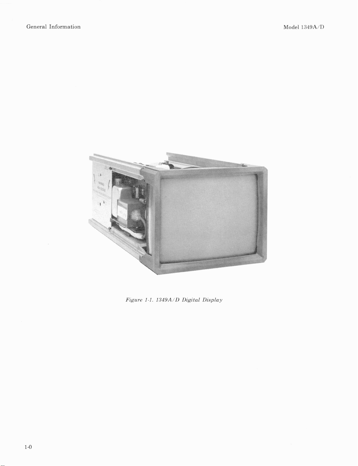
Figure 1-1. 1349A/D Digital Display
Page 9
Model 1349A/D
Scans by ArtekMedia © 2007
General Information
SECTION
GENERAL INFORMATION
1-1. INTRODUCTION.
1-2. This Operating and Service Manual contains
information required to install, operate, test, adjust, and
service the HP Model
1-3. Listed on the title page of this manual is a
microfiche part number. This number can be used to
order 4x6-inch microfilm transparencies of the manual.
Each microfiche contains up to 96 photo-duplicates of
the manual pages. Themicrofiche package also includes
the latest Manual Changes supplement.
1349A/D Digital Display.
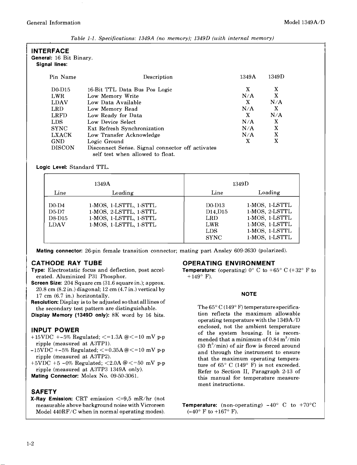
1-4. SPECIFICATIONS.
Instrument specifications are listed in table 1-1.
1-5.
These specifications are the performance standards or
limits against which the instrument is tested. Table
lists 1349A/D functions. Supplemental characteristics
are listed in table
typical characteristics included as additional informa-
tion for the user.
1-3 and are not specifications but are
1-2
1-6. SAFETY CONSIDERATIONS.
To prevent personal injury, observe all
safety precautions and warnings stated on
the instrument and in this manual.
1-7.
This product is a Safety Class 1 instrument. Review
the instrument and manual for safety markings and
instructions before operation. Specific warnings, cautions
and instructions are placed wherever applicable. Refer
to the Safety Summary in the front of this manual and to
Sections
These precautions must be observed
11, V, and VIII for further safety precautions.
duringall phases of
I
operation, service, and repair of this instrument. Failure
to comply with these precautions or with specific
warnings elsewhere in this manual violates safety
standard of design, manufacture, and intended use of
this instrument. Hewlett-Packard assumes no liability
for the customer's failure to comply with these
requirements.
1-8. INSTRUMENTS COVERED BY MANUAL.
Attached to the instrument is a serial number tag.
1-9.
The serial number is in the form:
parts; the first four digits and the letter are the serial
prefix, and the last five digits are the suffix. The prefix is
the same for all identical instruments. The suffix,
however, is assigned sequentially and is different for
each instrument. The contents of this manual apply to
instruments with the serial number
under SERIAL NUMBERS on the title page.
An instrument manufactured after the printing
1-10.
of this manual may have a serial number prefix that is
not listed on the title page. This unlisted serial number
prefix indicates that the instrument is different from
those described in this manual. The manual for this
newer instrument is accompanied by a Manual Changes
supplement. This supplement contains "change information" that explains how to adapt the manual to the
newer instrument.
1-11.
In addition to change information, the supplement may contain information for correcting errors in
the manual. The supplement for this manual is
identified with the manual print date and part number,
both of which appear on the manual title page.
1-12. For information concerning a serial number
prefix that is not listed on the title page or in the Manual
Changes supplement, contact your nearest HewlettPackard office.
0000A00000. It is in two
prefix(es) listed
Page 10
General Information Model 1349A/D
Scans by ArtekMedia © 2007
Table
1-1.
Specifications: 1349A (no memory); 13490 (with internal memory)
INTERFACE
General: 16 Bit Binary.
Signal lines:
Pin Name Description
DO-Dl5
LWR
LDAV
LRD
LRFD
LDS
SYNC
LXACK
GND
DISCON
16-Bit TTL Data Bus Pos Logic
Low Memory Write
Low Data Available
Low Memory Read
Low Ready for Data
Low Device Select
Ext Refresh Synchronization
Low Transfer Acknowledge
Logic Ground
Disconnect Sense. Signal connector off activates
self test when allowed to float.
Logic Level: Standard TTL.
1349A
Line Loading
1
DO-D4
D5-D7
-MOS, 1 -LSTTL, 1 -STTL
1
-MOS, 2-LSTTL, 1 -STTL
D8-Dl5 1-MOS, 1-LSTTL, 1-STTL
LDAV 1-MOS, 1-LSTTL, 1-STTL
Line Loading
DO-Dl3 1-MOS, 1-LSTTL
D14,D15 1-MOS, 2-LSTTL
LRD 1-MOS, 1-LSTTL
LWR 1-MOS, 1-LSTTL
1349D
LDS 1-MOS, 1-LSTTL
SYNC 1-MOS, 1-LSTTL
Mating connector: 26-pin female transition connector; mating part Ansley 609-2630 (polarized).
CATHODE RAY TUBE OPERATING ENVIRONMENT
Type: Electrostatic focus and deflection, post accel-
erated. Aluminized P31 Phosphor.
Screen Size: 204 Square cm (31.6 square in.); approx.
20.8 cm (8.2 in.) diagonal; 12 cm (4.7 in.) vertical by
17 cm (6.7 in.) horizontally.
Resolution:
Display is to be adjusted so that alllines of
the secondary test pattern are distinguishable.
Display Memory (1349D only): 8K word by 16 bits.
INPUT POWER
+
15VDC +-5% Regulated;
ripple (measured at
-15VDC +-5% Regulated; <=0.35A@<=10 mV p-p
ripple (measured at
+5VDC +5 -0% Regulated; <2.OA @ <=50 mV p-p
ripple (measured at
Mating Connector: Molex No. 09-50-3061.
<=
1.3A @<=lo mV p-p
A3TP1).
A3TP2).
A3TP3 1349A only).
Temperature: (operating) 0' C to +65' C (+32' F to
+14g0 F).
NOTE
The
65' C (149' F) temperaturespecifica-
tion reflects the maximum allowable
operating temperature with the
enclosed, not-the ambient temperature
of the system housing. It is recommended that a minimum of 0.84 m3/min
(30 ft3/min) of air flow is forced around
and through the instrument to ensure
that the maximum operating temperature of
Refer to Section
65' C (149' F) is not exceeded.
11, Paragraph 2-13 of
this manual for temperature measure-
ment instructions.
SAFETY
X-Ray Emission: CRT emission <=9,5 mR/hr (not
measurable above background noise with
Vicroreen
Model 440RF/C when in normal operating modes).
Temperature: (non-operating) -40' C to +70°C
(-40' F to +167' F).
1349A/D
Page 11
Model 1349A/D General Information
Scans by ArtekMedia © 2007
Table
1-1. Specifications (Cont'd)
Humidity:
Altitude:
to 95%) relative humidity up to +50° C.
(operating) to 4600 m, (15,000 ft);
(non-operating) to 15,300 m, (50,000 ft).
Shock:
Shock Intensity 60g.
11
Shock Pulse Duration
ms.
Shock tests are performed with the equipment
non-operating and any auxiliary circuits not powered.
Vibration:
Vibration Frequency: 5-55-5 Hz.
Vibration Sweep: Cover the vibration frequency in
15 minutes.
Vibration Pulse Shape: Full sine wave.
Vibration peak-to-peak amplitude:
5-10 Hz, 6.34 mm (0.250 in.)
10-25 Hz, 3.05 mm (0.120 in.)
25-55 Hz, 0.76 mm (0.030 in.)
Dwell for 10 minutes at the four highest resonances
found on each axis. If no major resonance can be
detected, dwell at 55 Hz for 10 minute duration at
0.76 mm (0.030 in.).
-
Table
Size:
Weight:
Shipping Weight:
-
-
1-2.
1349A/D Functions
1349A/D Displays have been
The
tested at shock and vibration levels
listed above. These are absolute maximum levels and apply to the
1349A/D
only not to the host structure in which
they are installed.
In general, the host structure will act
to amplify shock and vibration applied
to it when transmitting that energy to
1349A/D.
the
Care must be taken that specified
levels of shock and vibration are not
applied to the
1349A/D.
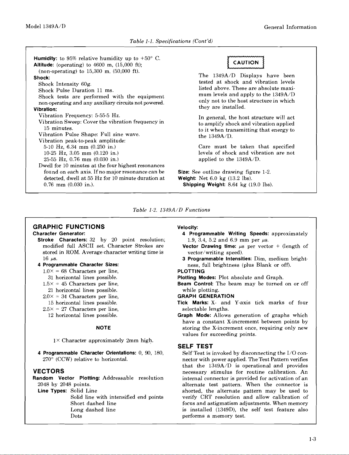
See outline drawing figure 1-2.
Net 6.0 kg (13.2 lbs).
8.64 kg (19.0 lbs).
GRAPHIC FUNCTIONS
Character Generator:
Stroke Characters:
modified full ASCII set. Character Strokes are
stored in ROM. Average character writing time is
16 ps.
4 Programmable Character Sizes:
1.0X = 68 Characters per line,
31 horizontal lines possible.
1.5X = 45 Characters per line,
21 horizontal lines possible.
2.0x = 34 Characters per line,
15 horizontal lines possible.
32 by 20 point resolution; 1.9, 3.4, 5.2 and 6.9 mm per ps.
Velocity:
4 Programmable Writing Speeds:
Vector Drawing time:
ps per vector + (length of
vector/writing speed).
3
Programmable Intensities:
Dim, medium bright-
ness, full brightness (plus Blank or off).
PLOTTING
Plotting Modes:
Beam Control:
Plot absolute and Graph.
The beam may be turned on or off
while plotting.
GRAPH GENERATION
Tick Marks:
X-
and Y-axis tick marks of four
approximately
2.5X = 27 Characters per line, selectable lengths.
12 horizontal lines possible.
Graph Mode:
Allows generation of graphs which
have a constant X-incrememt between points by
NOTE
storing the X-increment once, requiring only new
values for succeeding points.
lx
Character approximately 2mm high.
SELF TEST
4 Programmable Character Orientations:
270' (CCW) relative to horizontal.
VECTORS
Random Vector Plotting:
2048 by 2048 points. alternate test pattern. When the connector is
Line Types:
Solid Line shorted, the alternate pattern may be used to
Solid line with intensified end points verify CRT resolution and allow calibration of
Short dashed line
Long dashed line is installed
Dots performs a memory test.
Addressable resolution internal connector is provided for activation of an
0, 90, 180,
Self Test is invoked by disconnecting the
I/O connector with power applied. The Test Pattern verifies
that the
1349A/D is operational and provides
necessary stimulus for routine calibration. An
focus and astigmatism adjustments. When memory
(1349D), the self test feature also
Page 12
General Information Model 1349A/D
Scans by ArtekMedia © 2007
Table
1-3.
Supplemental Characteristics
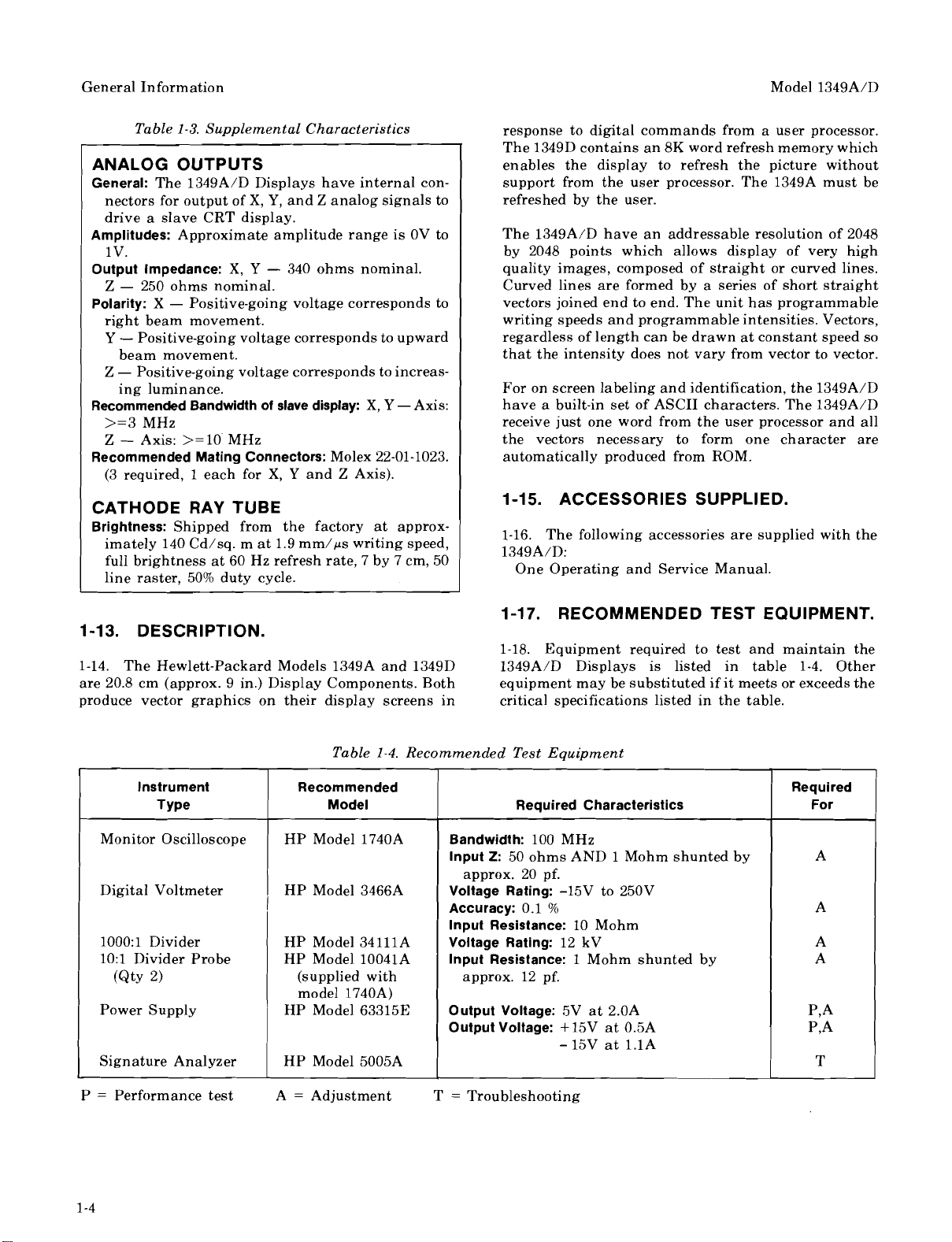
ANALOG OUTPUTS
General: The 1349A/D Displays have internal con-
nectors for output of
drive a slave CRT display.
Amplitudes: Approximate amplitude range is OV to
1 v.
Output Impedance:
Z
-
250 ohms nominal.
Polarity: X -
right beam movement.
Y
-
Positive-going voltage corresponds to upward
beam movement.
Z
-
Positive-going voltage corresponds to increas-
ing luminance.
Recommended Bandwidth of slave display:
>=3 MHz
Z
-
Axis:
Recommended Mating Connectors: Molex 22-01-1023.
(3 required,
Positive-going voltage corresponds to
>=
1 each for
X,
X,
Y
10 MHz
Y,
and Z analog signals to
-
340 ohms nominal.
X,
Y
-Axis:
X,
Y
and Z Axis).
CATHODE RAY TUBE
Brightness: Shipped from the factory at approx-
imately 140
full brightness at 60 Hz refresh rate, 7 by 7 cm, 50
line raster, 50% duty cycle.
Cd/sq. m at 1.9 mm/ps writing speed,
response to digital commands from a user processor.
1349D contains an 8K word refresh memory which
The
enables the display to refresh the picture without
support from the user processor. The
refreshed by the user.
1349A/D have an addressable resolution of 2048
The
by 2048 points which allows display of very high
quality images, composed of straight or curved lines.
Curved lines are formed by a series of short straight
vectors joined end to end. The unit has programmable
writing speeds and programmable intensities. Vectors,
regardless of length can be drawn at constant speed so
that the intensity does not vary from vector to vector.
For on screen labeling and identification, the
have a built-in set of ASCII characters. The 1349A/D
receive just one word from the user processor and all
the vectors necessary to form one character are
automatically produced from ROM.
1-15.
1-16. The following accessories are supplied with the
1349A/D:
ACCESSORIES SUPPLIED.
One Operating and Service Manual.
1349A must be
1349A/D
1-17.
RECOMMENDED TEST EQUIPMENT.
1-13. DESCRIPTION.
1-18. Equipment required to test and maintain the
1-14. The Hewlett-Packard Models
are 20.8 cm (approx. 9 in.) Display Components. Both equipment may be substituted if it meets or exceeds the
produce vector graphics on their display screens in critical specifications listed in the table.
Instrument
Monitor Oscilloscope
Digital Voltmeter
1000:l Divider
10:l Divider Probe
(Q~Y 2)
Power Supply
1
Signature Analyzer
-
P = Performance test
I
I
HP Model 1740A
HP Model 3466A
HP Model 34111A
HP Model 10041A
HP Model 633153
HP Model
A = Adjustment
1349A and 1349D 1349A/D Displays is listed in table 1-4. Other
Table
1-4.
Recommended Test Equipment
Recommended
Model
(supplied with
model
1740A)
5005A
Required Characteristics
Bandwidth: 100 MHz
lnput
2:
50 ohms AND 1 Mohm shunted by
approx. 20 pf.
Voltage Rating: -15V to 250V
Accuracy: 0.1
lnput Resistance: 10 Mohm
Voltage Rating: 12 kV
lnput Resistance:
approx. 12 pf.
Output Voltage: 5V at 2.OA
Output Voltage:
r
=
Troubleshooting
96
1
Mohm shunted by
+
15V at 0.5A
-
15V at 1.lA
Required
For
Page 13
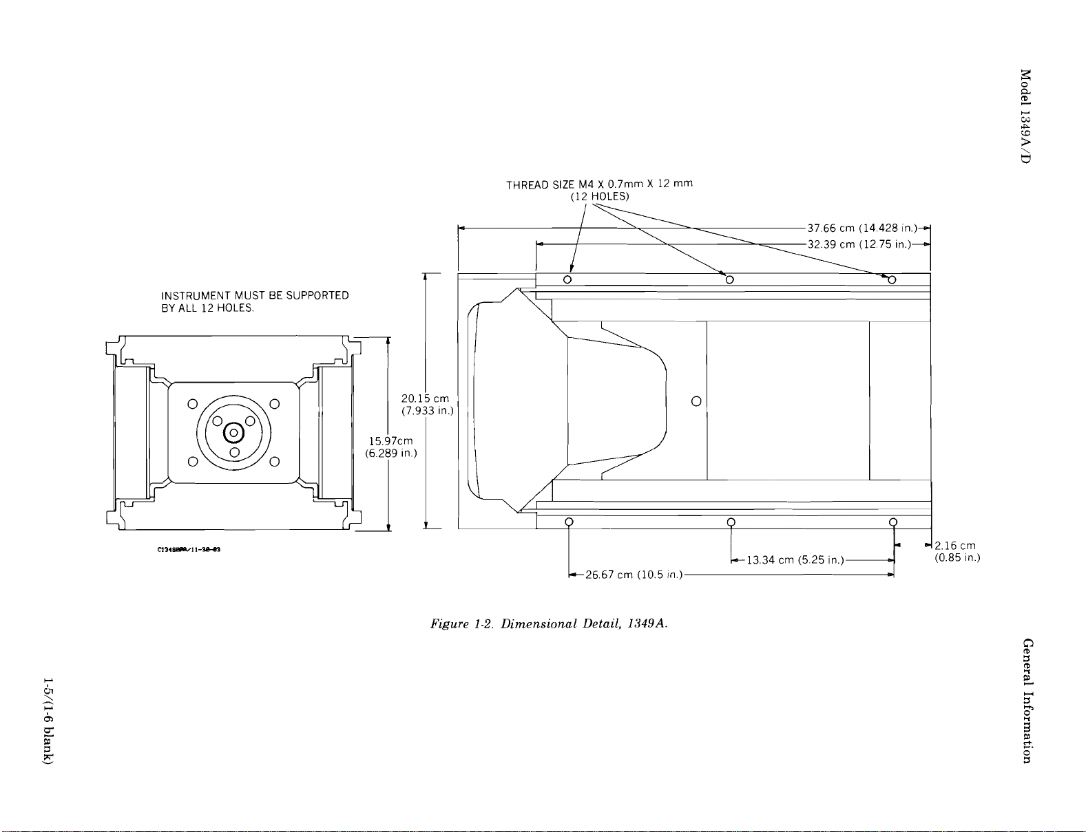
INSTRUMENT MUST BE SUPPORTED
Scans by ArtekMedia © 2007
12
BY ALL
HOLES.
20.1
(7.9
7c
m
9 in.)
I
3
crn
in.)
THREAD SIZE M4
(12
X
0.7rnrn
HOLES)
X
12
rnrn
Figure
1-2.
Dimensional Detail,
1349A.
Page 14
Model 1349A/D
Scans by ArtekMedia © 2007
Installation
SECTION II
INSTALLATION
2-1. INTRODUCTION.
This section provides installation instructions for
2-2.
the Model
includes information about initial inspection, damage
claims, preparation for use, and storage and shipment.
1349A/D Digital Displays. This section also
2-3. INITIAL INSPECTION.
2-4. Inspect the shipping container for damage. If the
shipping container or cushioning material is damaged,
it should be kept until the contents of the shipment
have been checked for completeness and the instrument
has been checked mechanically and electrically. The
contents of the shipment should be as listed in the
"Accessories Supplied" paragraph in Section I. Procedures for checking electrical performance are given
in Section IV. If the contents are incomplete, if there is
mechanical damage or defect, or if the instrument does
not pass the Performance Tests, notify the nearest
Hewlett-Packard office. If the shipping container is
damaged, or the cushioning material shows signs of
Table
2-1. 1349A/D
stress, notify the carrier as well as the Hewlett-Packard
office. Keep the shipping material for carrier's inspection.
The HP office will arrange for repair or replacement at
HP option without waiting for claim settlement.
2-5. PREPARATION FOR USE.
WARNING
u
Read the Safety Summary in the front of
this manual and the "Safety Considerations" paragraph in Section I before installing or operating this instrument. Before any
connections are made to the instrument, the
chassis must be connected to a safety
ground.
2-6. POWER REQLIIREMENTS.
2-7. The 1349A/D requires the following power
supplies for proper operation:
Power
Requirements
Operating Voltages
Voltage
+15 VDC
-15 VDC
+5 VDC
Tolerance
+5-0%
+-5%
+-5%
Max
P-P
Ripple
10 mV
10 mV
50 mV
Max Current
1349D
1.3A
350 mA
2.OA
1349A
1.3A
350 mA
750 mA
Page 15
Installation Model 1349A/D
Scans by ArtekMedia © 2007
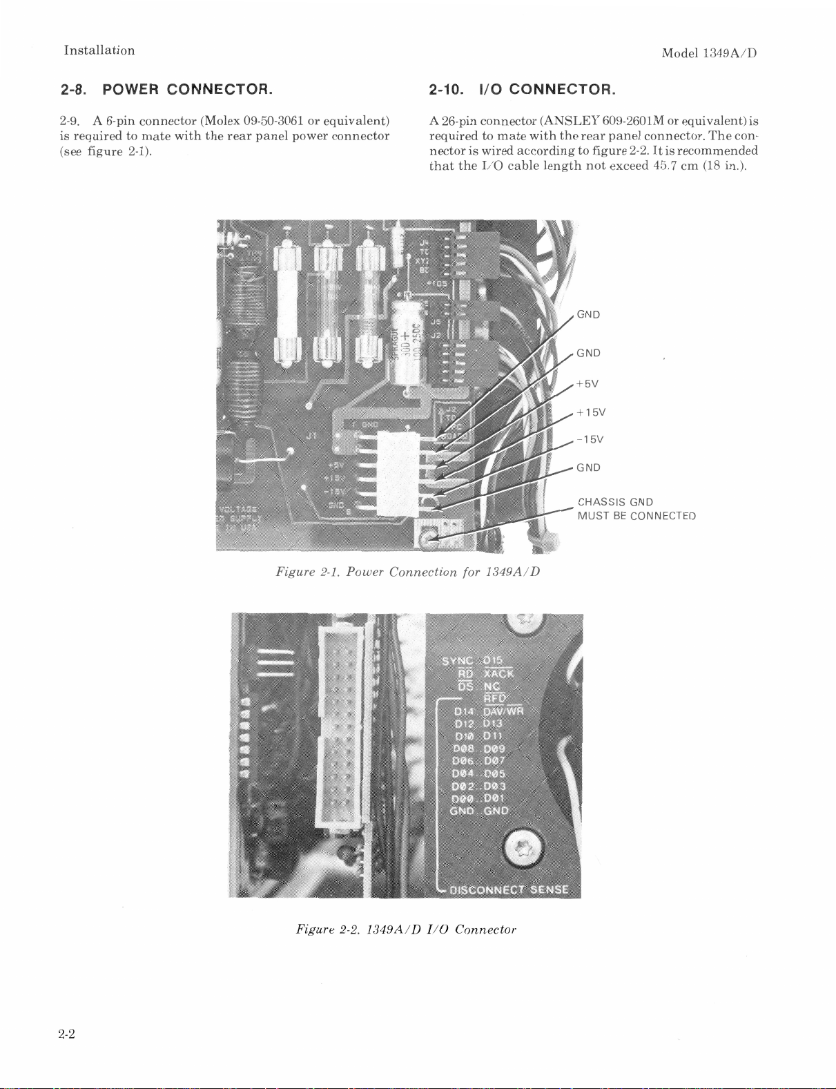
2-8.
2-9.
POWER CONNECTOR.
A 6-pin connector (Molex 09-50-3061 or equivalent)
is required to mate with the rear panel power connector
(see figure 2-1).
2-10.
1/O CONNECTOR.
A 26-pin connector (ANSLEY 609-2601M or equivalent) is
required to mate with the rear panel connector. The connector is wired according to figure 2-2. It is recommended
that the
I/O
cable length not exceed 45.7 cm (18 in.).
Figure 2-1. Power Connection for 1349A/D
SIS
GND
-
BE CONNECTED
Figure 2-2. 1349A/D
Z/O
Connector
Page 16
Model 1349A/D
Scans by ArtekMedia © 2007
Installation
2-1 1. ANALOG OUTPUTS
The purpose of the Analog Output jacks on the X-YZ/Stroke Generator (Al) board is to connect an
external X-Y-Z display. The output signals can drive
p-p into 600 ohm loads. The bandwidth of the external
X-Y-Z display should have the following bandwidths:
X-Y Axis: >=3 MHz
Z Axis: >=lo MHz
The interface cables should not exceed
length. Use the following table for interfacing:
A1J3
A1J4
A1J5
........
.......
.......
Z AXIS OUTPUT
Y AXIS OUTPUT
X AXIS OUTPUT
(X-Y-Z).
1V
1.83m (6 ft) in
2-12. OPERATING ENVIRONMENT.
2-13. Temperature.
in temperatures from
The airflow recommendations stated above
must be adhered to in order to prevent
damage to the instrument.
The 65"
reflects the maximum allowable operating
temperature with the
the ambient temperature of the system
housing. It is recommended that a minimum
of .84
around and through the instrument to ensure
that the maximum operating temperature of
65"
Ambient temperature measurements should be taken at
several points in the instrument. Use the following information as a guide for making these measurements:
Measure temperature at:
Focus Gain Adjustment.
and the Memory Board (A5) near
C
m3/min (30 ft3/min) of air flow is forced
C
(+14g0 F) is not exeeded.
a. Between the High Voltage cover and
b. 0.64 cm (0.25 in.) above
c. Between Vector Processor Board (A2)
d. 0.64 cm (0.25 in.) above AlU23.
The instrument may be operated
0" C to f65" C (+32" F to 149" F).
NOTE
(+
149" F) temperature specification
1349A/D enclosed, not
A4R31.
A2U16.
2-14. Humidity.
environments with humidity up to
instrument should also
extremes which cause condensation within the
instrument.
2-15. Altitude.
altitudes up to 4 600m (15 000 ft).
The instrument may be operated in
95%. However, the
be
protected from temperature
The instrument may be operated at
2-16. STORAGE AND SHIPMENT.
2-17. Environment.
shipped in environments within the following limits:
Temperature
Humidity up to
Altitude
The instrument should also be protected from temperature extremes which causes condensation within the
instrument.
The instrument may be stored or
-40" C to $70" C (-40" F to +158" F)
95g1 relative humidity at
+50° C (+122" F)
15 300m (50 000 ft)
2-18. PACKAGING.
2-19. Original Packaging.
identical to those used in factory packaging are
available through Hewlett-Packard offices. If the
instrument is being returned to Hewlett-Packard for
servicing, attach a tag indicating the type of service
required, return address, model number, and full serial
number. Also mark the container FRAGILE to ensure
careful handling. In any correspondence, refer to the
instrument by model number and full serial number.
2-20. Other Packaging.
tions should be used for repacking with commercially
available materials.
a. Wrap instrument in antistatic plastic. (If shipping
to Hewlett-Packard office or service center, attach a tag
indicating type of service required, return address,
model number, and full serial number).
b. Use a strong shipping container. A double-wall
carton made of 350-pound test material is adequate.
c. Use a layer of shock-absorbing material 70 to 100
mm (3 to
instrument to provide firm cushioning and prevent
movement inside the container. Protect control panel
with cardboard.
d. Seal shipping container securely.
4
inches) thick around all sides of the
Containers and materials
The following general instruc-
The surface temperature near AlU26 and AlU33
typically may be +50° C (+12Z0 F) or more above the
ambient temperature. It is therefore recommended that
heat-sensitive devices or circuits not
proximity to these points.
be
placed in close
e. Mark shipping container FRAGILE to ensure
careful handling.
f. In any correspondence, refer to instrument by
model number and full serial number.
2-3/(2-4 blank)
Page 17
Model 1349A/D
Scans by ArtekMedia © 2007
Operation
SECTION
OPERATION
3-1. INTRODUCTION.
3-2. The purpose of this section is to give detailed
information concerning the operation and programming
1349A/D. It includes a list of the programming
of the
instructions and a section containing a brief
explanation of "bit programming". The end of this
section contains several programming examples.
WARNING
SHOCK HAZARD
Before operating the instrument, connect the
chassis of the display to a safety ground in
the system.
3-3. SIGNAL LINE DEFINITIONS.
DO-Dl5
DO through Dl4 are the vector data lines (TTL
positive logic).
instruction. When
recognized as a memory command. When
"0" then all the input data forms the picture.
DISCONNECT SENSE
This line must be grounded to the display chassis
when the data lines are active. The internal
Performance Verification pattern will be displayed
if the 26-pin connector is disconnected.
SYNC
External display refresh synchronization signal
line. The line provides an external refresh clock
when external sync mode has been selected via a
jumper wire on the Vector Memory board.
LXACK
Acknowledge signal line. When low, this line
indicates that the Vector Memory has completed
the Read or Write operation requested by the user
processor.
Dl5 is used as a Vector Memory
Dl5 is a"1" then theinput data is
Dl5 is a
Ill
LDS
Device Select signalline. When low this line enables
the Vector Memory to communicate with the user
processor
LWR
Memory Write signal line. When low, this line
indicates that the 16-bit Data Bus contents
written into either the current Vector Memory
location
(D15=1).
LRD
Memory Read signal line. When low, this line
indicates that the contents of the current Vector
Memory location (as specified by the User Address
Pointer) are to be placed on the 16-bit Data Bus for
transmission back to the user processor.
Whenever a Vector Memory location has
been either written into or read from by the
user processor, the User Address Pointer
auto-increments to the next Vector Memory
location (address).
3-4. HANDSHAKE TIMING FOR 1349D.
The TTL digital interface to the Vector Memory (1349D)
is compatible with most microprocessor peripheral
interface adaptor chips (the Motorola
Vector Memory digital interface consists of:
1. A 16-bit bidirectional Data Bus.
2. A Read Signal line LRD (input).
3. A Write signal line LWR (input).
4. A Device Select signal line
5. An Acknowledge signal line LXACK (output).
6. An External display Synchronization signal line
SYNC (input use is optional).
(write/read).
areto be
(D15=0) or into the User Address Pointer
NOTE
63
6821).
LDS (input).
Page 18
Operation
Scans by ArtekMedia © 2007
Model
1349A/D
A
Tdss
READ
COMMFWD
4
TIMING
Tdsh
4
Tdh
MI349001
Read Command Timing
Tdss
-
Device Select Setup Time
Tdsh - Device Select Hold Time
-
Trd
Trdp - Read Precharge Time
Tac - Read Access Time
Tdh - Read Data Hold Time
Tah - Acknowledge Hold Time
Tack - Acknowledge Delay Time
Read Pulse Time (ACK not used) 495 nsec min
(ACK used) 760 nsec min
..........
............
..........
Figure
3-1.
Read Command Timing
.......
........
760 nsec max
........
130 nsec max
455 nsec min
.....
855 nsec max
0 nsec min
0 nsec min
25
nsec min
30 nsec min
40 nsec min
Page 19
Model 1349A/D
Scans by ArtekMedia © 2007
Operation
4
Tdss
HRITE
1-
COMmWD
TCY
TIMING
4
Tdsh
4
Write Command Timing
Tdss
-
Device Select Setup Time
Tdsh
-
Device Select Hold Time
-
Tcy
Twe
Tds
Tdh - Data In Hold Time 0 nsec min
Tack
Tah
Write Cycle Time
-
Write Command Active Time
-
Data In Setup Time
-
acknowledge Delay Time
-
Acknowledge Hold Time..
Figure
3-2.
Write Command Timing
..............
........
........
820 nsec min
. .
795 nsec rnin
.............
..............
.....
455 nsec min
855 nsec max
.......
130 nsec max
0 nsec min
0 nsec min
0 nsec max
40 nsec min
Page 20
Operation
Scans by ArtekMedia © 2007
P/O
RS
(MEMORY
BD.
1349D)
SWITCHES SET
FOR
INT SYNC
1349A/D
Model
SWITCHES SET
FOR
EXT
SYNC
Figure
3-3.
Refresh Mode Selection
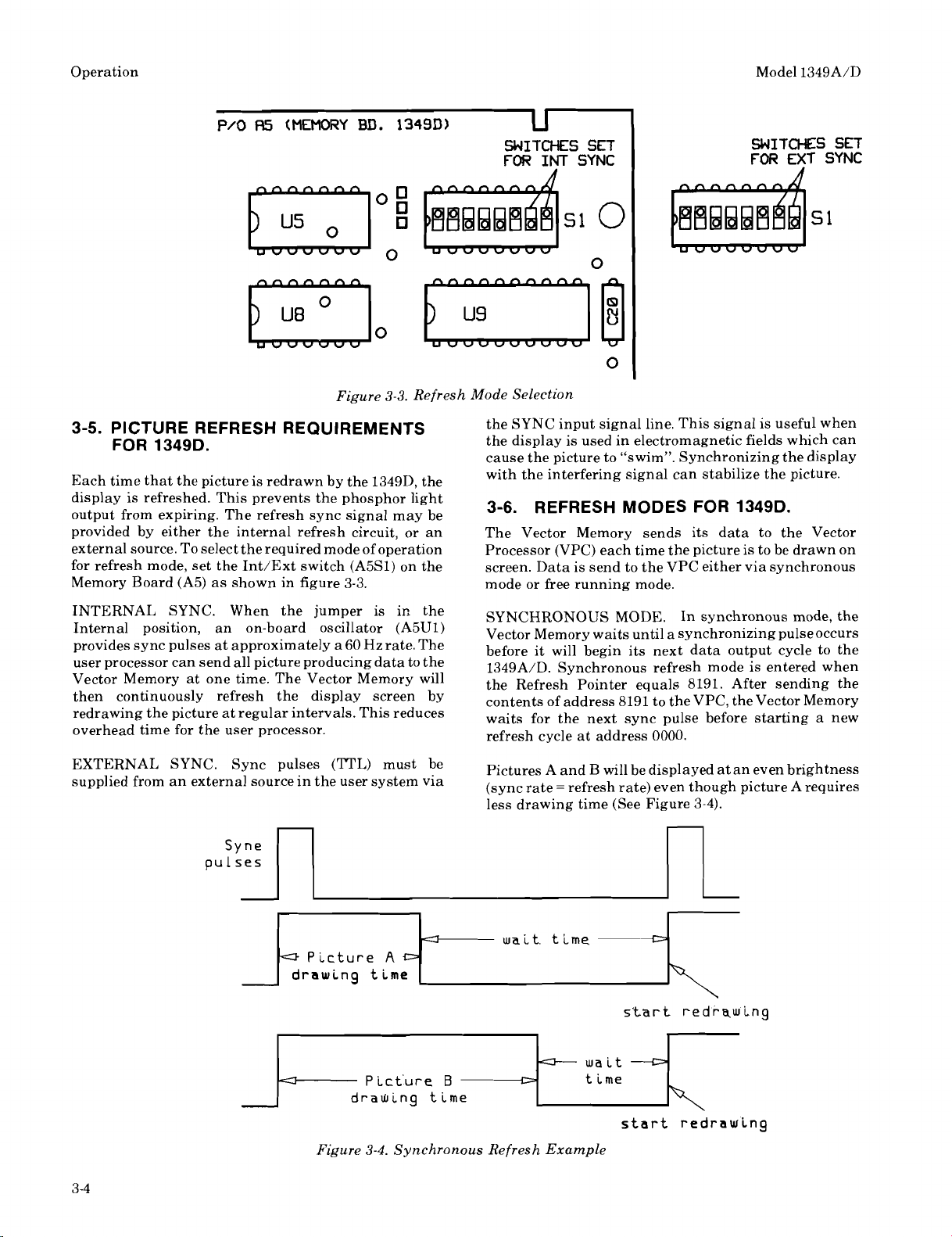
3-5. PICTURE REFRESH REQUIREMENTS
1349D.
FOR
Each time that the picture is redrawn by the 1349D, the
display is refreshed. This prevents the phosphor light
output from expiring. The refresh sync signal may be
provided by either the internal refresh circuit, or an
external source. To select the required mode of operation
for refresh mode, set the
Memory Board (A5) as shown in figure 3-3.
INTERNAL SYNC. When the jumper is
Internal position, an on-board oscillator
provides sync pulses at approximately a
user processor can send all picture producing data to the
Vector Memory at one time. The Vector Memory will
then continuously refresh the display screen by
redrawing the picture at regular intervals. This reduces
overhead time for the user processor.
EXTERNAL
supplied from an external source in the user system via
SYNC.
Int/Ext switch (A5S1) on the
ir, the
(A5U1)
60
Hz rate. The
Sync
pulses (?TL)
must
be
the SYNC input signal line. This signal is useful when
the display is used in electromagnetic fields which can
cause the picture to "swim". Synchronizing the display
with the interfering signal can stabilize the picture.
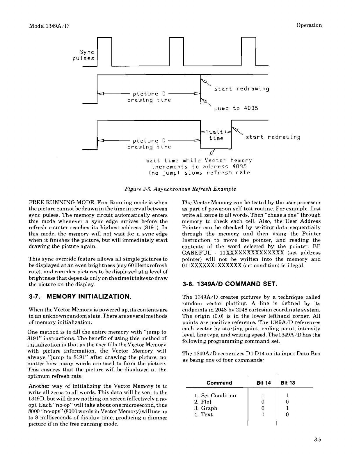
3-6. REFRESH MODES FOR 1349D.
The Vector Memory sends its data to the Vector
Processor (VPC) each time the picture is to be drawn on
screen. Data is send to the VPC either via synchronous
mode or free running mode.
SYNCHRONOUS MODE.
Vector Memory waits until a synchronizing pulseoccurs
before it will begin its next data output cycle to the
1349A/D. Synchronous refresh mode is entered when
the Refresh Pointer equals 8191. After sending the
contents of address 8191 to the VPC, the Vector Memory
waits for the next sync pulse before starting a new
refresh cycle at address
Pictures A and B will be displayed atan even brightness
=
(sync rate
less drawing time (See Figure
refresh rate) even though picture A requires
In synchronous mode, the
0000.
3-4).
-
-
5
Picture
drawing time
4
Figure
Pict'ure
drauing time
3-4.
4
ruait. time
A
B
LS
Synchronous Refresh Example
-0
rua
it
time
start
redrsrulng
start redrawing
\
Page 21
Model 1349A/D
Scans by ArtekMedia © 2007
Operation
I=-
1
-a
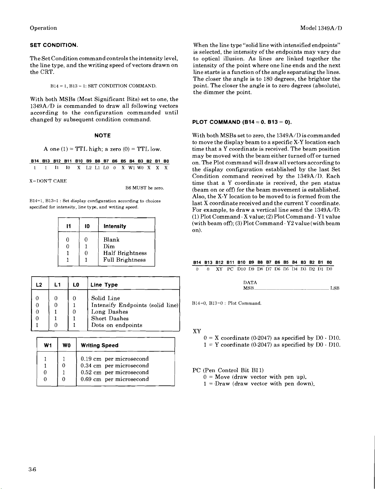
FREE RUNNING MODE. Free Running mode is when
the picture cannot be drawn in the time interval between
sync pulses. The memory circuit automatically enters
this mode whenever a sync edge arrives before the
refresh counter reaches its highest address (8191). In
this mode, the memory will not wait for a sync edge
when it finishes the picture, but will immediately start
drawing the picture again.
This sync override feature allows all simple pictures to
be displayed at an even brightness (say 60 Hertzrefresh
rate), and complex pictures to be displayed at a level of
brightness that depends only on the time it takes to draw
the picture on the display.
picture
drawing time
picture
drawing time
Figure
3-5.
C
D
uait time while Vector Memory
increments to address 4095
(no
jump1 slows refresh rate
Asynchronous Refresh Example
start redrawing
\
Jump to 4095
await
time
-\
start redrawing
P
The Vector Memory can be tested by the user processor
as part of power-on self test routine. For example, first
write all zeros to all words. Then "chase a one" through
memory to check each cell. Also, the User Address
Pointer can be checked by writing data sequentially
through the memory and then using the Pointer
Instruction to move the pointer, and reading the
contents of the word selected by the pointer. BE
CAREFUL
pointer) will not be written into the memory and
OllXXXXXXlXXXXXX (set condition) is illegal.
3-8. 1349AlD COMMAND SET.
-
1lXXXXXXXXXXXXXX (set address
3-7. MEMORY
When the Vector Memory is powered up, its contents are endpoints in 2048 by 2048 cartesian coordinate system.
in an unknown random state. There are several methods The origin
of memory initialization.
One method is to fill the entire memory with ''jump to
8191" instructions. The benefit of using this method of
initialization is that as the user fills the Vector Memorv
with picture information, the Vector Memory will
always "jump to 8191" after drawing the picture, no
matter how many words are used to form the picture.
This ensures that the picture will be displayed at the
optimum refresh rate.
Another way of initializing the Vector Memory is to
write all zeros to all words. This data will be sent to the
1349D, but will draw nothing on screen (effectively a noop). Each "no-op" will take about one microsecond, thus
8000 "no-ops" (8000 words in Vector Memory) will use up
to 8 milliseconds of display time, producing a dimmer
picture if in the free running mode.
INITIALIZA'rION.
The 1349A/D creates pictures by a technique called
random vector plotting. A line is defined by its
(0,O) is in the lower lefthand corner. All
points are positive reference. The
each vector by starting point, ending point, intensity
level,
line
type,
and
writing
following
The
as being one of four commands:
programming
1349A/D recognizes DO-Dl4 on its input Data Bus
Command
1. Set Condition
2. Plot
3. Graph
4. Text
speed,
command
4
1349A/D references
The
1349A/D
set.
Bit
14
Bit
13
has
the
Page 22
Operation
Scans by ArtekMedia © 2007
Model
1349A/D
SET CONDITION.
The Set Condition command controls theintensity level,
the line type, and the writing speed of vectors drawn on
the CRT.
B14 = 1, B13 - 1: SET CONDITION COMMAND.
With both MSBs (Most Significant Bits) set to one, the
1349A/D is commanded to draw all following vectors
according to the configuration commanded until
changed by subsequent condition command.
NOTE
A
one (1) = TTL high; a zero (0) = TTL low.
X=
DON'T CARE
B6 MUST be zero.
B14=1, B13-1 : Set display configuration according to choices
specified for intensity, line type, and writing speed.
1
11 1 10
1
intensity
I
When the line type "solid line with intensified endpoints"
is selected, the intensity of the endpoints may vary due
to optical illusion. As lines are linked together the
intensity of the point where one line ends and the next
line starts is a function of the angle separating the lines.
The closer the angle is to 180 degrees, the brighter the
point. The closer the angle is to zero degrees (absolute),
the dimmer the point.
PLOT COMMAND (B14
With both MSBs set to zero, the
to move the display beam to a specific X-Y location each
time that a Y coordinate is received. The beam position
may be moved with the beam either turned off or turned
on. The Plot command will draw all vectors according to
the display configuration established by the last Set
Condition command received by the
time that a Y coordinate is received, the pen status
(beam on or off) for the beam movement is established.
Also, the X-Y location to be moved to is formed from the
last X coordinate received and the current Y coordinate.
For example, to draw a vertical line send the
(1) Plot Command - X value; (2) Plot Command - Y1 value
(with beam off); (3) Plot Command
on).
=
0.
B13 = 0).
1349A/D is commanded
1349A/D. Each
1349A/D:
-
Y2 value (with beam
-
L2
0
0
0
0
1
W1
1
1
0
0
L1
0
0
1
1
0
Half Brightness
Full Brightness
Line Type
LO
Solid Line
0
Intensify Endpoints (solid line)
1
Long Dashes
0
1
Short Dashes
1
Dots on endpoints
WO
Writing Speed
0.19 cm per microsecond
1
0
0.34 cm per microsecond
0.52 cm per microsecond
1
0
0.69 cm per microsecond
DATA
MSB LSB
B14=0, B13=0 : Plot Command.
XY
0 = X coordinate (0-2047) as specified by DO - D10.
1
=
Y coordinate (0-2047) as specified by DO - D10.
PC (Pen Control Bit B11)
0 = Move (draw vector with pen up).
1
=,Draw (draw vector with pen down).
Page 23
Model 1349A/D
Scans by ArtekMedia © 2007
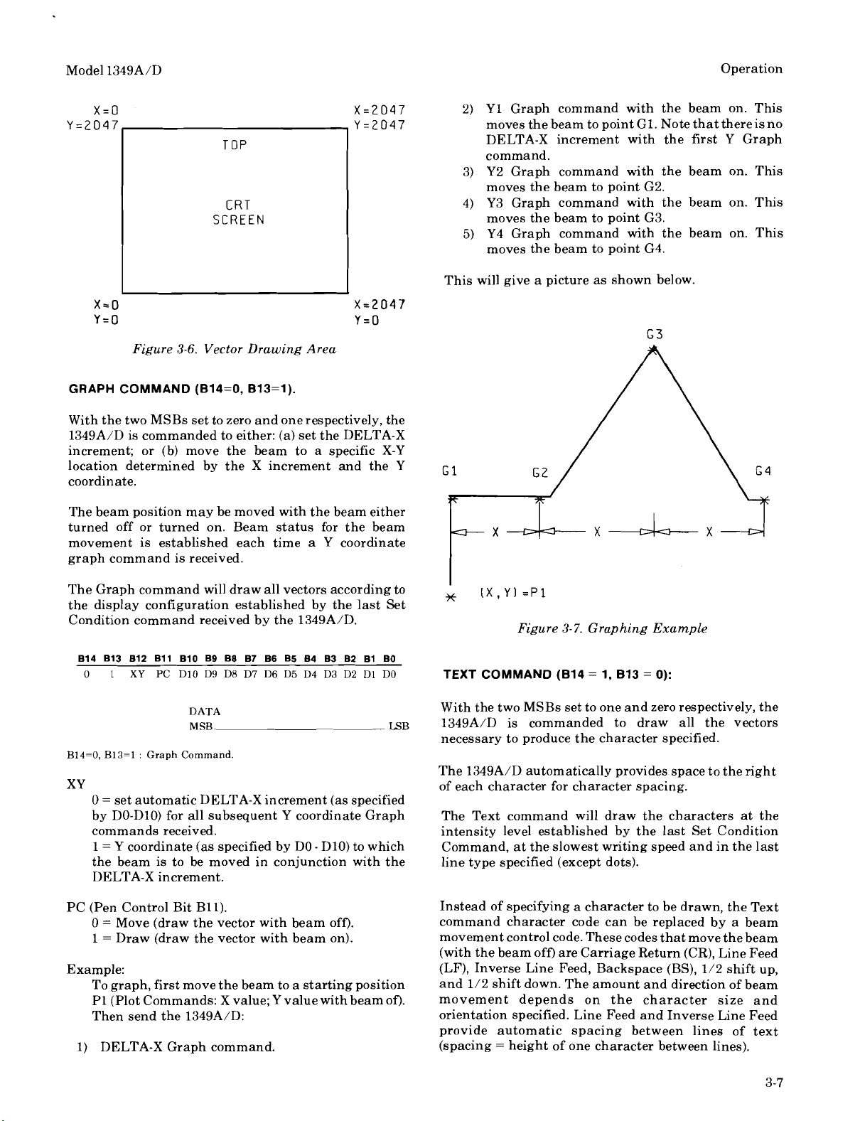
TOP
CRT
SCREEN
Operation
2) Y1 Graph command with the beam on. This
moves the beam to point
GI. Note that thereis no
DELTA-X increment with the first Y Graph
command.
Y2
3)
Graph command with the beam on. This
moves the beam to point G2.
Y3 Graph command with the beam on. This
4)
moves the beam to point G3.
5)
Y4 Graph command with the beam on. This
moves the beam to point G4.
This will give a picture as shown below.
Figure
GRAPH COMMAND (B14=0, B13=1).
3-6.
Vector Drawing Area
With the two MSBs set to zero and onerespectively, the
1349A/D is commanded to either: (a) set the DELTA-X
increment; or (b) move the beam to a specific X-Y
location determined by the X increment and the Y
coordinate.
The beam position may be moved with the beam either
turned off or turned on. Beam status for the beam
movement is established each time a
Y
coordinate
graph command is received.
The Graph command will draw all vectors according to
the display configuration established by the last Set
Condition command received by the
DATA
MSB
B14=0, B13=1
:
Graph Command
1349A/D.
LSB
XY
0 = set automatic DELTA-X increment (as specified
by DO-DIO) for all subsequent Y coordinate Graph
commands received.
1
=
Y
coordinate (as specified by DO - D10) to which
the beam is to be moved in conjunction with the
DELTA-X increment.
*
IX,Yl
=P1
Figure
TEXT
COMMAND (814 = 1, 813
3-7.
Graphing Example
=
0):
With the two MSBs set to one and zero respectively, the
1349A/D is commanded to draw all the vectors
necessary to produce the character specified.
The
1349A/D automatically provides space to the right
of each character for character spacing.
The Text command will draw the characters at the
intensity level established by the last Set Condition
Command, at the slowest writing speed and in the last
line type specified (except dots).
PC (Pen Control Bit
0 = Move (draw the vector with beam off).
1
=
Draw (draw the vector with beam on).
Example:
To graph, first move the beam to a starting position
P1 (Plot Commands: X value; Y value with beam of).
Then send the
1) DELTA-X Graph command.
Bll).
1349A/D:
Instead of specifying a character to be drawn, the Text
command character code can be replaced by a beam
movement control code. These codes that move the beam
(with the beam off) are Carriage Return (CR), Line Feed
(LF), Inverse Line Feed, Backspace (BS),
and
1/2 shift down. The amount and direction of beam
1/2 shift up,
movement depends on the character size and
orientation specified. Line Feed and Inverse Line Feed
provide automatic spacing between lines of text
(spacing
=
height of one character between lines).
Page 24
Operation Mode1 1349A/D
Scans by ArtekMedia © 2007
The starting point for non-rotated characters is the
lower left-hand corner of the character area. Forrotated
characters the entire character area is rotated the
specified number of degrees (90, 180, or 270) in a
counterclockwise direction around the starting point.
When the
1349A/D has finished drawing a character it
automatically advances the beam to the starting point
for the next character. In this way the
1349A/D
functions much like a typewriter when presenting text.
The modified ASCII character set for the
1349A/D is
shown in table 3-1.
814 813 812 Bll B10 B9 BE 87 B6 B5 84 83 82 B1 BO
1 0 S1 SO R1 RO ES D7
CHARACTER
MSB LSB
B14=1. B13=0
:
commands that the
(specified
by
DO - D7)
D6
D5 D4 D3 D2 Dl DO
1349A
display a text character
ES (Establish size of character Bit B8).
0 = use previous size and rotation.
1
=
establish new size and rotation according to
S1-SO and
R1-RO.
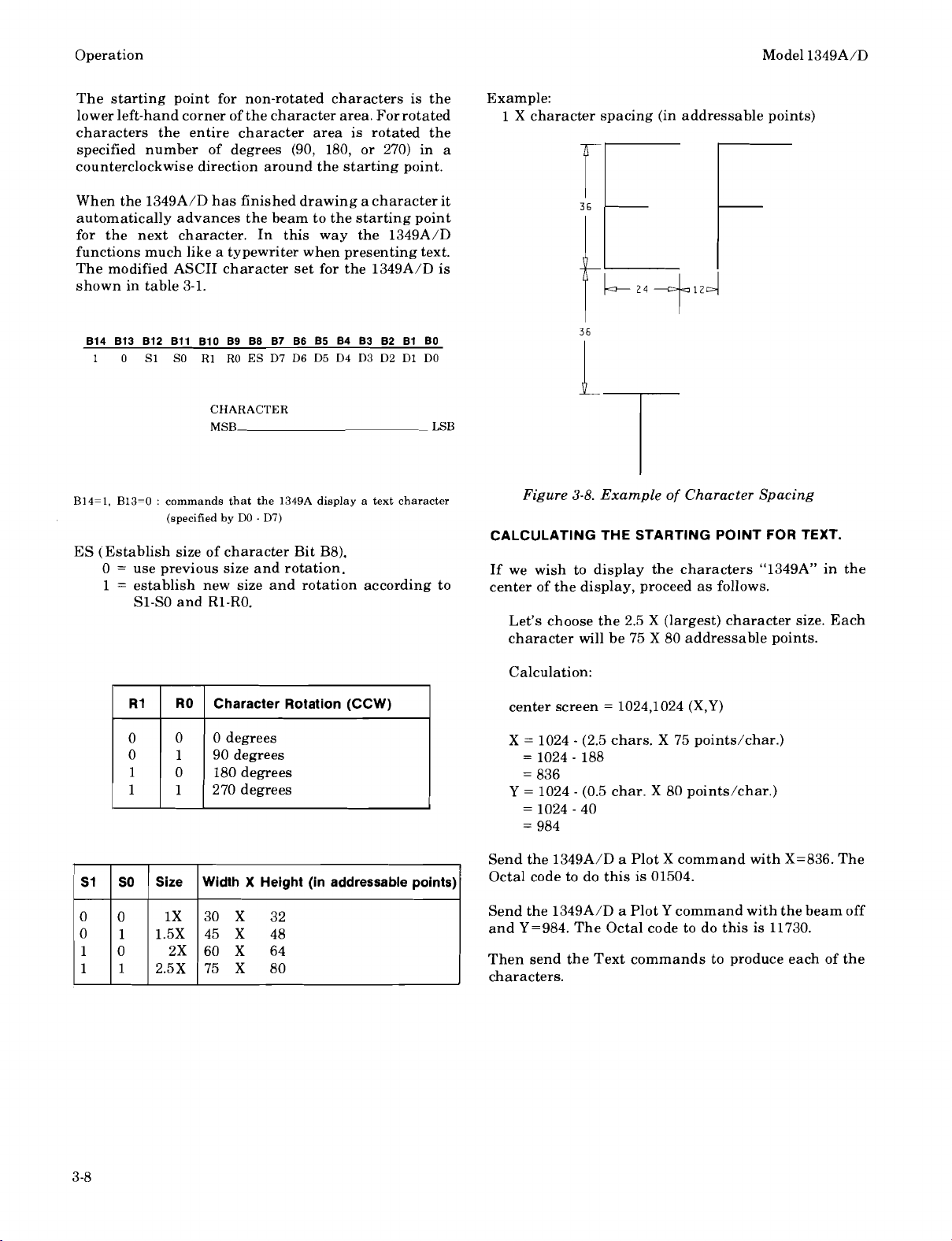
Example:
1
X character spacing (in addressable points)
Figure
CALCULATING THE STARTING POINT FOR TEXT.
If we wish to display the characters
center of
3-8.
Example
of
Character Spacing
"1349A" in the
the display, proceed as follows.
Let's choose the 2.5 X (largest) character size. Each
character will be 75 X 80 addressable points.
R1
0
0
1
1
1
S1
0
0
Size
SO
0
1.5X
1
10
1
2.5X
1
RO
Character Rotation (CCW)
0 degrees
0
90 degrees
1
180 degrees
0
270 degrees
1
Width X Height (in addressable points)
1X
30
X
32
45
X 48
2X
60
X
64
75 X 80
Calculation:
center screen
=
1024,1024 (X,Y)
X = 1024 - (2.5 chars. X 75 points/char.)
=
1024 - 188
=
836
Y
=
1024 - (0.5 char. X 80 points/char.)
=
1024 - 40
=
984
Send the 1349A/D a Plot X command with X=836. The
Octal code to do this is 01504.
Send the
and
1349A/D a Plot Y command with the beam off
Y=984. The Octal code to do this is 11730.
Then send the Text commands to produce each of the
characters.
Page 25
Model 1349A/D Operation
Scans by ArtekMedia © 2007
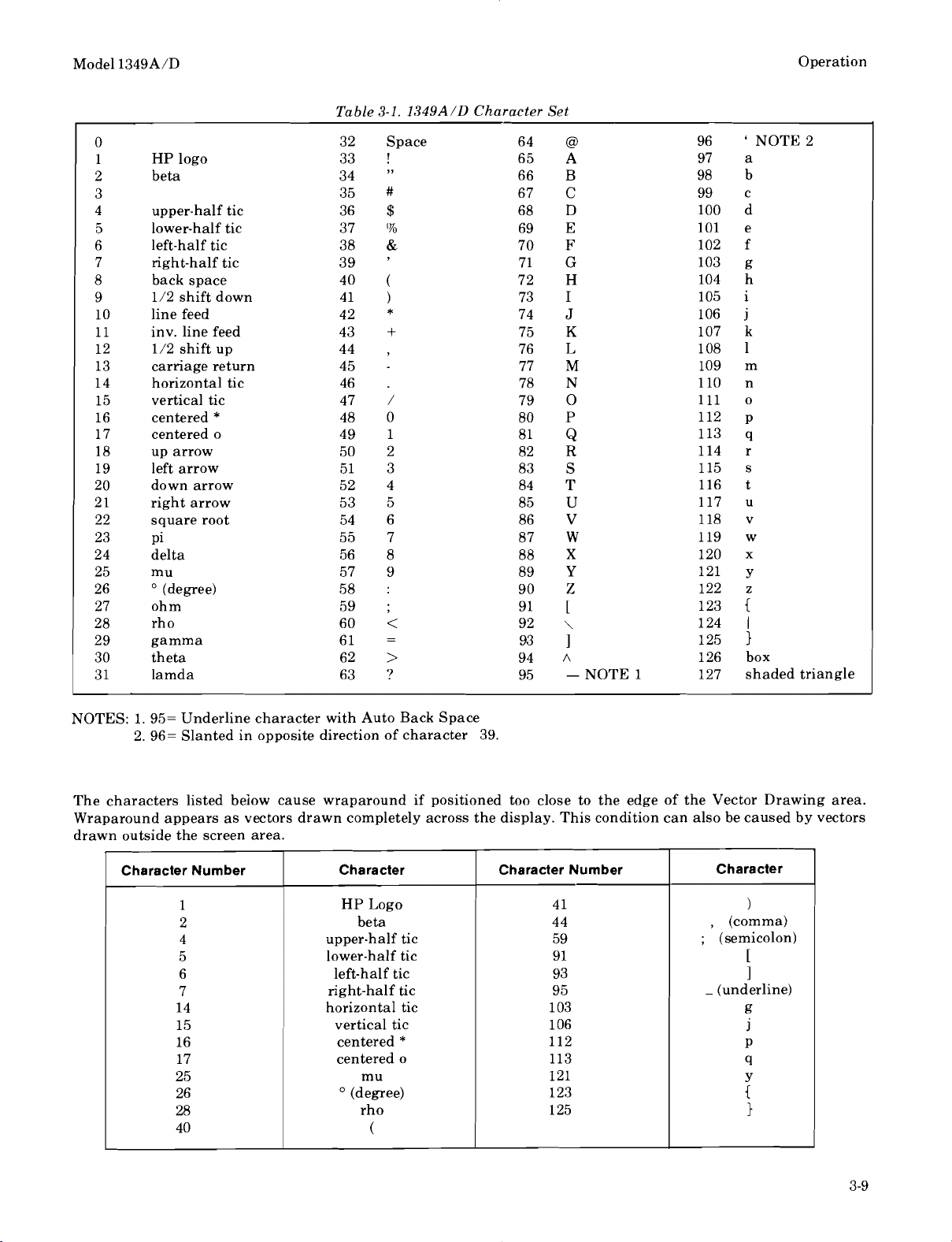
Table
HP logo
beta
upper-half tic
lower-half tic
left-half tic
right-half tic
back space
1/2 shift down
line feed
inv. line feed
1/2 shift up
carriage return
horizontal tic
vertical tic
centered
*
centered o
up arrow
left arrow
down arrow
right arrow
square root
pi
delta
mu
O (degree)
ohm
rho
gamma
theta
lamda
3-1. 1349A/D
32 Space
33
34
35 #
36
37
38
39
40
42
43
44
45
49
55 7
58
60
61
!
"
$
'%
&
'
(
41
*
+
,
-
46 .
47
48 0
50 2
51 3
52 4
53 5
54 6
56 8
57 9
:
59
;
<
=
62
>
63
?
/
1
Character Set
@
A
B
C
D
E
F
G
H
I
J
K
L
M
N
0
P
Q
R
S
T
u
v
W
X
Y
z
[
\
I
A
-
NOTE 1
'
NOTE 2
a
b
C
d
e
f
g
h
i
j
k
1
m
n
0
P
q
r
s
t
U
v
W
X
Y
z
E
box
shaded triangle
NOTES:
1. 95= Underline character with Auto Back Space
2. 96= Slanted in opposite direction of character
39.
The characters listed below cause wraparound if positioned too close to the edge of the Vector Drawing area.
Wraparound appears as vectors drawn completely across the display. This condition can also be caused by vectors
drawn
outside the screen area.
Character Number
1
2
4
5
6
7
14
15
16
17
25
26
28
40
Character
HP Logo
beta
upper-half tic
lower-half tic
left-half tic
right-half tic
horizontal tic
vertical tic
centered
*
centered o
mu
(degree)
rho
(
Character Number
41
4 4
59
91
93
95
103
106
112
113
121
123
125
Character
1
,
(comma)
;
(semicolon)
[
1
-
(underline)
g
j
P
q
f
I
Page 26
Operation Mode1 1349A/D
Scans by ArtekMedia © 2007
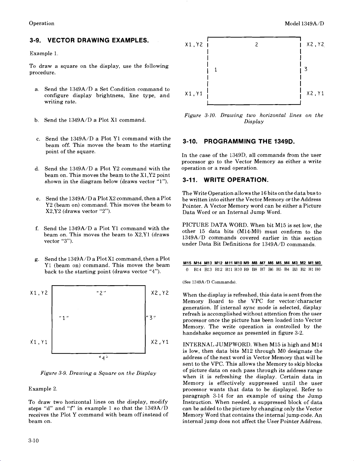
3-9. VECTOR DRAWING EXAMPLES.
Example 1.
To draw a square on the display, use the following
procedure.
a.
Send the
1349A/D a Set Condition command to
configure display brightness, line type, and
writing rate.
b. Send the
c. Send the
1349A/D a Plot X1 command. Display
1349A/D a Plot Y1 command with the
beam off. This moves the beam to the starting
point of the square.
Send the
d.
beam on. This moves the beam to the
shown in the diagram below (draws vector
Send the 1349A/D a PlotX2 command, then aplot
e.
1349A/D a Plot Y2 command with the
Xl,Y2 point
"1").
Y2 (beam on) command. This moves the beam to
X2,Y2 (draws vector "2").
f.
Send
the
beam
1349A/D a 'lot
On.
This
the
command
beam
to
X2'Y1
with
(draws
the
vector "3").
I
I
I
I
I
l'Y1
I
J
Figure
3-10.
In the case of the
processor go to the Vector Memory as either a write
operation or a read operation.
3-1 1 WRITE OPERATION-
The Write Operation allows the 16 bits on thedata bus to
be written into either the Vector Memory or the Address
Pointer. A Vector Memory word can be either a Picture
Data Word or an Internal Jump Word.
PICTURE DATA WORD. When bit M15 is set low, the
other 15 data bits (M14-MO) must
1349A/D commands covered earlier in this section
under Data Bit Definitions for
3-10.
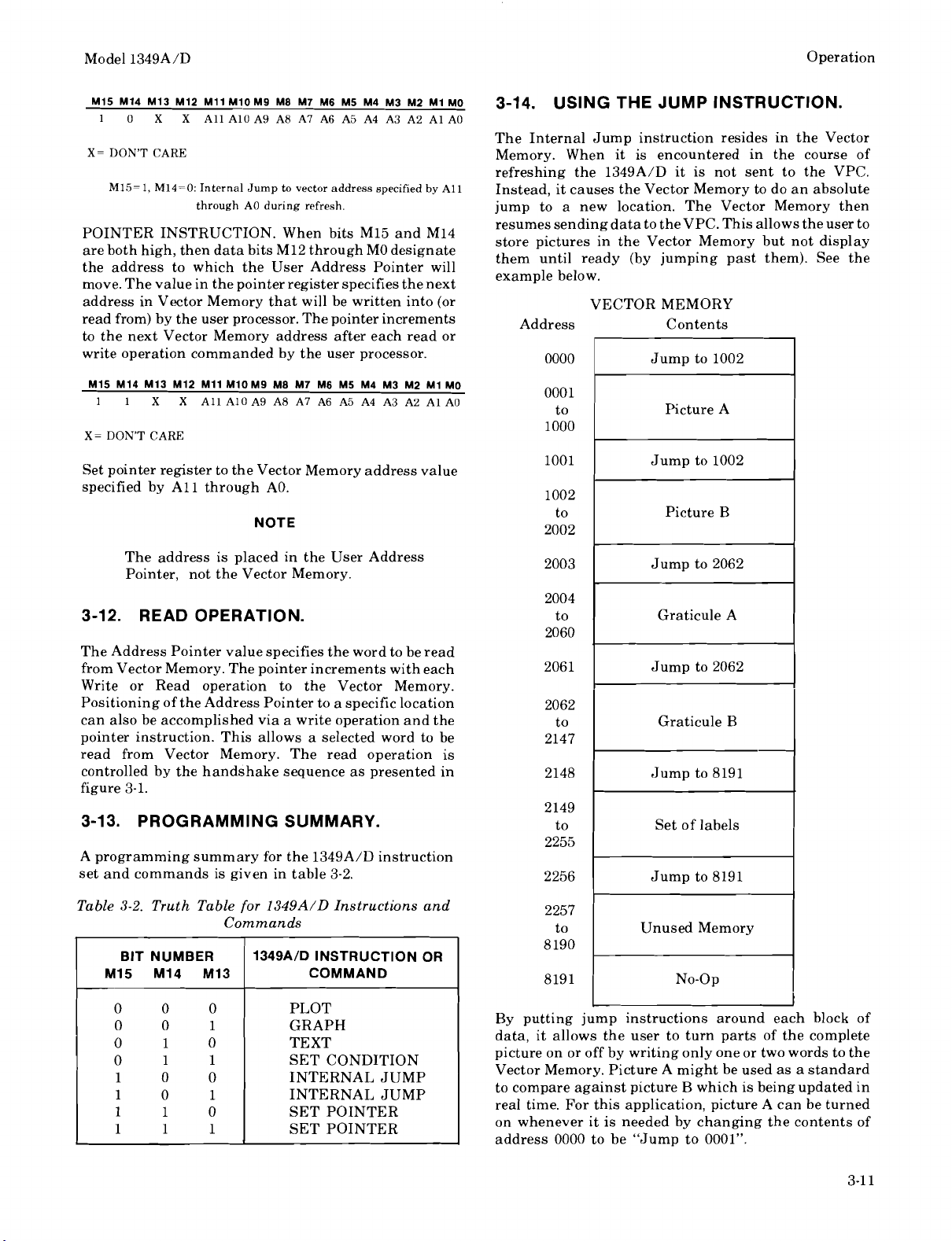
Drawing two horizontal lines on the
THE
1349D.
1349D, all commands from the user
conform
1349A/D commands.
I
I
X2,Yl
I
I
to the
g.
Send the
1349A/D a Plot X1 command, then a Plot
Y1 (beam on) command. This moves the beam
back to the starting point (draws vector "4").
Figure
3-9.
Drawing a Square on the Display
Example 2.
To draw two horizontal lines on the display, modify
"f'
steps "d" and
in example 1 so that the 1349A/D
receives the Plot Y command with beam off instead of
beam on.
MI5 M14 MI3 MI2 Mll Mi0 M9 M8 M7 M6 M5 M4 M3 M2 MI MO
0 B14 B13 B12 B11 BIO B9
(See
1349A/D
Commands)
I38
B7
B6
I35
B4
B3
B2 B1 BO
When the display is refreshed, this data is sent from the
Memory Board to the VPC for
vectodcharacter
generation. If internal sync mode is selected, display
refresh is accomplished without attention from the user
processor once the picture has been loaded into Vector
Memory. The write operation is controlled by the
handshake sequence as presented in figure 3-2.
INTERNAL JUMPWORD. When M15 is high and M14
is low, then data bits M12 through MO designate the
address of the next word in Vector Memory that will be
sent to the VPC. This allows the Memory to skip blocks
of picture data on each pass through its address range
when it is refreshing the display. Certain data in
Memory is effectively suppressed until the user
processor wants that data to be displayed. Refer to
paragraph 3-14 for an example of using the Jump
Instruction. When needed, a suppressed block of data
can be added to the picture by changing only the Vector
Memory Word that contains the internal jump code. An
internal jump does not affect the User Pointer Address.
Page 27
Model 1349A/D
Scans by ArtekMedia © 2007
Operation
3-14. USING THE JUMP INS'TRUC'TION.
X=
DON'T
CARE
M15= 1, M14=0:
Internal Jump to vector address specified
through
A0
during refresh.
by
All
POINTER INSTRUCTION. When bits M15 and M14
are both high, then data bits M12 through MO designate
the address to which the User Address Pointer will
move. The value in the pointer register specifies the next
address in Vector Memory that will be written into (or
read from) by the user processor. The pointer increments
to the next Vector Memory address after each read or
write operation commanded by the user processor.
X=
DON'T
CARE
Set pointer register to the Vector Memory address value
specified by All through AO.
NOTE
The address is placed in the User Address
Pointer, not the Vector Memory.
The Internal Jump instruction resides in the Vector
Memory. When it is encountered in the course of
refreshing the
1349A/D it is not sent to the VPC.
Instead, it causes the Vector Memory to do an absolute
jump to a new location. The Vector Memory then
resumes sending data to the VPC. This allows the user to
store pictures in the Vector Memory but not display
them until ready (by jumping past them). See the
example below.
VECTOR MEMORY
Address Contents
Jump to 1002
Picture A
Jump to 1002
Picture B
Jump to 2062
3-12. READ OPERATION.
The Address Pointer value specifies the word to be read
from Vector Memory. The pointer increments with each
Write or Read operation to the Vector Memory.
Positioning of the Address Pointer to a specific location
can also be accomplished via a write operation and the
pointer instruction. This allows a selected word to be
read from Vector Memory. The read operation is
controlled by the handshake sequence as presented in
figure 3-1.
3-13. PROGRAMMING SUMMARY.
A programming summary for the 1349A/D instruction
set and commands is given in table 3-2.
Table
3-2.
Truth Table for
1349A/D
Instructions and
Commands
BIT NUMBER
MI5 MI4 MI3
0 0 0
0 0
0
0
1
1
1
0 0
1 0
1
1
1
1
1349AlD INSTRUCTION OR
COMMAND
PLOT
1
0
1
GRAPH
TEXT
SET CONDITION
INTERNAL JUMP
1
0
1
INTERNAL JUMP
SET POINTER
SET POINTER
Graticule A
Jump to 2062
Graticule B
Jump to 8191
Set of labels
Jump to 8191
Unused Memory
NO-Op
By putting jump instructions around each block of
data, it allows the user to turn parts of the complete
picture on or off by writing only one or two words to the
Vector Memory. Picture A might be used as a standard
to compare against picture B which is being updated in
real time. For this application, picture A can be turned
on whenever it is needed by changing the contents of
address 0000 to be "Jump to
0001".
Page 28
Operation Model 1349A/D
Scans by ArtekMedia © 2007
NOTE
Vector Memory location 0000 is the first
location sent to the
cycle. The Vector Memory then
ments to location 0001, 0002, etc.
1349A/D in each refresh
auto-incre-
3-15. OPTIMIZING PlCTLlRE QUALITY
Due to differing conditions of ambient light when the
1349A/D is displaying pictures, the programmer may
have to experiment with the Intensity and Writing
Speed parameters of the Set Condition command.
For example, in an environment of high ambient light,
the
1349A/D should be set to the highest brightness
level and slowest writing speed.
3-16. OCTAL AND HEXADECIMAL RANGES
1349AlD COMMANDS.
FOR
1349AlD
Command
Plot
X
(beam off)
Y
Y
(beam on)
Graph
Set DELTA-X
Y
(beam off)
Y
(beam on)
Octal Range
00000 - 07777
10000 - 13777
14000
-
17777
-
20000
30000
34000
27777
-
33777
-
37777
Hexadecimal
Range
0000 - OFFF
1000 - 17FF
1800
-
lFFF
2000 - 2FFF
3000 - 37FF
3800
-
3FFF
3-17. OPERATING CONSIDERATIONS FOR
THE
1349A.
Model 1349A is not equipped with the Vector Memory
Board.
3-18. SIGNAL LINE DEFINI'TIONS.
DO-D15.
DO through Dl5 are the vector data lines ('M'L positive
logic). Bit
LDAV
Data Valid Signal Line (active low
processor to
data bus.
LRFD
Ready for data signal line (active low). Signal to user
processor.
DISCONNECT SENSE.
This line must be grounded when above signal lines
are active. The internal performance verification
pattern will be displayed if this line in not grounded.
Dl5 is used only with the Memory Board.
).
Signal from user
1349A. New output data is available on
1349A is ready for next data transfer.
-
-
. .
. . . . . . . .
57777
77777
-
Text
Set Condition
Internal Jump
Set Pointer
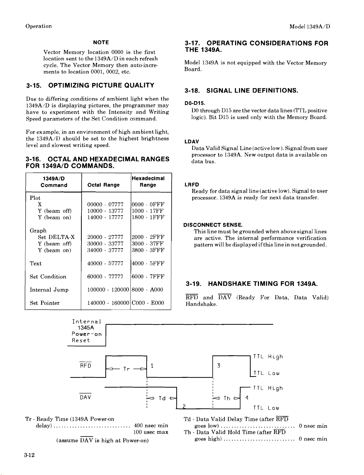
Tr - Ready Time (1349A Power-on
delay)
. . . . . . . . . . . . . . .
40000
60000
100000 - 120000
140000
Internal
1345A
Power-on
Reset
-
DAV
-
(assume DAV is high at Power-on)
160000
. . . .
-
5FFF
4000
6000 - 7FFF
8000 - A000
COO0 - EOOO
k-
Td
400 nsec min
100 usec max
3-19. HANDSHAKE TIMING FOR 1349A.
-
RFD and DAV (Ready For Data, Data Valid)
Handshake.
-
7
Td
-
Data Valid Delay Time (after RFD
goes low)
-
Data Valid Hold Time (after FD
Th
goes high)
-
-
TTL High
. . .
4
. . . . . .
TTL Lou
.
. . .
hTh~
I
.
. . . . . . . . . . . . . . . . . . . . . . .
. . .
-
. . . . . . . .
. . .
.
.
0 nsec min
. .
0 nsec min
Page 29
Model 1349A/D
Scans by ArtekMedia © 2007
Operation
3-20. TRANSFER SEQUENCE.
1.
1349A sets RFD low to indicate that it is ready for a
word from the 16-bit Data Bus.
2. User processor sets DAV low to indicate that the
contents of the 16-bit Data Bus are valid.
1349A returns RFD high to indicate that it has
3.
accepted the word from the 16-bit Data Bus.
4. User processor returns DAV high so that the
1349A
can initiate the next transfer.
5.
1349A sets RFD low to indicate that it is ready for a
word from the 16-bit Data Bus.
3-21. RESTRICTIONS.
1.
User processor can set DAV low at the same time
or after
2. User processor can return DAV high at the same
time or after
BEFORE.
1349A sets RFD low, but NOT BEFORE.
1349A returns RFD high, but NOT
NOTE
While DAV remains low, the 1349A will not
act on the command from the
DataBus, even
though it has signalled that it has accepted
the word from the Data Bus. It is recommended that the host system keep Th to a
minimum.
3.
1349A will not set RFD low unless DAV is
high.
4.
Data on the 16-bit Data Bus must remain
valid as long as DAV is low.
NOTE
For maximum speed and performance, it is
advisable that the host system use EDGE
TRIGGERED logic.
3-13/(3-14 blank)
Page 30
Model 1349A/D
Scans by ArtekMedia © 2007
Performance Tests
SECTION IV
PERFORMANCE VERIFICATION
4-1.
4-2. The Performance Verification Procedures in this
section test the instrument's electrical performance.
The procedures provide approximately 90% assurance
of proper
4-3.
4-4. Equipment required for the performance tests is
listed in Section
satisfies the critical specifications given in the table
may be substituted for the recommended models.
4-5.
4-6.
required for this instrument. Performance tests should
be performed after service work has been performed or
if improper operation is suspected.
INTRODUCTION.
1349A/D operation.
EQUIPMENT REQUIRED.
I,
table 1-4. Any equipment that
CALIBRATION CYCLE.
Periodic performance verification is not normally
PERFORMANCE TESTS
4-9.
PERFORMANCE VERIFICATION.
4-7. Further checks that require access to the interior
of the instrument are included in the adjustment
section, but are not required for the performance
verification.
WARNING
u
ELECTRICAL SHOCK HAZARD
This instrument is designed and manufactured for OEM systems. Protective covers
are not provided and internal hazardous
voltages are exposed when power is applied.
Component replacement, including fuses,
and internal adjustments must be made by
qualified maintenance personnel.
4-8.
PERFORMANCE TEST PROCEDURES.
DESCRIPTION:
The following procedure is directed at obtaining the correct performance verification pattern on the 1349A/D
screen.
EQUIPMENT REQUIRED:
Power Supply
Power Connector
PROCEDURE:
a. Adjust power supply outputs to values shown in table 4-1.
Table
4-1.
Power Supply Output
Operating Voltages
Max P-P Ripple
Voltage
+15 VDC
-15 VDC
+5 VDC
b. Connect power supply to the 1349A/D and turn on power. (See figure 4-1 for power connections.)
Tolerance
+-5%
+-5%
+-5%
10
mV
10 mV
50 mV
-
1349D
350 mA
Max Current
1349A
1.3A
350 mA
2.OA
750 mA
1.3A
Page 31

Performance Tests
Scans by ArtekMedia © 2007
Model
1349A/D
P/O
A3
L.V.P.S.
PERFORMANCE
Figure
4-1. 1349A/D
TESTS
Power Connections
GND
+5v
+
15V
-1
5V
GND
CHASIS GND
BE
MUST
CONNECTED
c. Check for a display as shown in figure
Figure
The
1349A/D
of the test pattern and the
displayed, refer to Section
cycles through the four Commands: Set Condition, Plot, Graph and Text Command. The relationship
1349A/D
VIII,
Commands is shown in figure
Service and Troubleshooting.
4-2.
4-2.
1349A/D
Primary Test Pattern
4-3.
If any portion of the test pattern is not
Page 32

Model
Scans by ArtekMedia © 2007
1349A/D
GRAPH COMMAND
PLOT COMMAND
PERFORMANCE TESTS
Performance Tests
SIZE AND ROTATION
TEXT
iP/O
TEXT COMMAND)
BOXES CHECK
"--CHARACTER GENERATOR
(P/O TEXT COMMAND)
,LINE
TYPES
TEXT COMMAND
(P/O TEXT COMMAND)
d. If a test pattern as shown in figure
Service and Troubleshooting.
SEVEN SEGMENT
CORRECT WRITING SPEED
Figure 4-3. 1349A/D Command Check-out
4-4
is
displayed, then the memory circuit is defective. Refer to Section VIII,
LINE INDICATES
Figure 4-4. Memory Fail Test Pattern (13490 only)
Page 33

Performance Tests Model 1349A/D
Scans by ArtekMedia © 2007
4-10.
DESCRIPTION:
RESOLUTION VERIFICATION.
PERFORMANCE
TESTS
An internal test pattern is used to check resolution.
EQUIPMENT REQUIRED:
Power Supply
Power Connector
PROCEDURE:
a. Disconnect the 1349A/D
I/O
Port (A2J4) and apply power.
b. Short A2J6-1 to A2J6-2 and display the focus and resolution test pattern (see figure 4-5).
c. To check resolution:
The 1349A/D passes the resolution test if every one of the lines in the 13 boxes can be resolved. Should the test
V
fail, perform the Focus and Astigmatism Adjustments described in Section
of this manual.
Figure 4-5. 1349A/D Focus and Resolution Test Pattern
Page 34

Model
Scans by ArtekMedia © 2007
1349A/D
Adjustments
SECTION
ADJUSTMENTS
5-1. INTRODUCTION.
This section describes adjustments and checks
5-2.
required to return the
capabilities when repairs have been made. Included in
this section are equipment setups and adjustment
procedures.
5-3. SAFETY REQUIREMENTS.
Although this instrument has been designed in
5-4.
accordance with international safety standards,
general safety precautions must be observed during all
phases of operation, service and repair of the
instrument. Failure to comply with the precautions
listed in the Safety Summary at the front of this manual
or with specific warnings given throughout this manual
could result in serious injury or death. Service and
adjustments should be performed only by qualified
service personnel.
1349A/D
to peak operating
V
5-9. ADJUSTMENT PROCEDURES.
SHOCK HAZARD
This instrument is designed and manufactured for OEM systems. Protectivecovers
are not provided and internal hazardous
voltages are exposed when power is applied.
Voltages up to
CRT and HVPS areas and are capable of
causing serious injury or death. Before any
connections are made to the instrument, the
chassis must be connected to a safety
ground. Component replacement, including
fuses, and internal adjustments must be
made by qualified maintenance personnel.
Table
5-1.
20
kV are present around the
Sequence
of
Adjustments
5-5 EQUIPMENT REQUIRED.
5-6.
A complete list of required test equipment is given
in Section
recommended may be substituted, provided it meets the
required characteristics. For best results, use recently
calibrated test equipment.
1,
table
1-4.
Test equipment equivalent to that
5-7. ADJUSTMENTS.
5-8.
The adjustment procedures are arranged in a
recommended sequence of adjustments. While most
adjustments may be made independent of other
adjustments, it is recommended that adjustments be
made sequentially as a number of adjustments are
directly related to preceeding or following adjustments.
5-1
15
for
For best results, allow the instrument to warm up for
minutes before making adjustments. See table
sequence of adjustments.
Adjustment
Low Voltage Power Supply
High Voltage Power Supply
Z-Axis Drive and Test
Pattern Set-up
Preliminary Focus and
Astigmatism
Intensity Cut-Off Level
Trace Alignment and
Writing Speed
Stroke Generator
Stroke Intensity
Image Size and Position
Vector Closure
Fine Focus and Astigmatism
Resolution Check
X-Y-Z
Auxiliary
Output Check
Amplifier
Order
of
Adjustment
1
2
3
4
5
6
7
8
9
10
11
12
13
Paragraph
No.
5-10
5-11
5-12
5-13
5-14
5-15
5-16
5-17
5-18
5-19
5-20
5-20
1
5-2
Page 35

Adjustments
Scans by ArtekMedia © 2007
ADJUSTMENTS
Model
1349A/D
LOW VOLTAGE
POWER SUPPLY A3
HlGH VOLTAGE
POWER SUPPLY A4
MP1 MAIN FRAME
\
1349A
TOP
VlEW
M2 CRT SHIELD
I
V1 CRT
\
A4A1 HlGH VOLTAGE MULTIPLIER
M
P4
BEZEL
A2 J4
1/0
PORT
Figure
5-1.
1349A/D
1349A
Assembly
BOTTOM
Location Identification
BOARD
'~5 MEMORY BOARD
VlEW
Page 36

Model 1349A/D Adjustments
Scans by ArtekMedia © 2007
ADJUSTMENTS
5-10.
LOW VOLTAGE POWER SUPPLY ADJUSTMENT.
REFERENCE:
Service Sheet
DESCRIPTION:
In this procedure the input power supplies are verified and the +105V power supply is adjusted to + 105V + 250 mV.
EQUIPMENT:
Digital Voltmeter
Power Supply
PROCEDURE:
a.
Preset the Intensity
when power is applied to the instrument.
b.
Apply power to the power connector on the Low Voltage Power Supply Board
supplies as indicated below:
4
(AlR128) and Intensity Cut-off AIR131 fully ccw. This step is done to protect the CRT
(A3J1) and check input power
Monitor supply Test Limits
c. Monitor
-
A3TP4
Reference
Designator
with the digital voltmeter and adjust the +105V supply for 105V k250 mV
A3R10
Adjustment
Name
+
105V Adjust
A3TP4
+105V
Table 5-2. +105V Adjustment.
Adjustment
Paragraph
5-10, c
A3R10
+I05
ADJUST +5V -1
A3TP3
Service
Sheet
4
A3TP2 A3TP1
5V
Description
Adjust for + 105V
f
250
mV
+15V
IEC
TOR
CONNECTED FOR PROPER OPERATION
Figure 5-2. Low Voltage Power Supply Adjustment Locations
5-3
Page 37

Adjustments Model 1349A/D
Scans by ArtekMedia © 2007
ADJUSTMENTS
5-11.
HIGH VOLTAGE POWER SUPPLY ADJUSTMENT.
REFERENCE:
Service Sheet 5.
DESCRIPTION:
This procedure describes the Cathode Voltage adjustment. The Cathode Voltage is set to -2450V, t25V.
EQUIPMENT REQUIRED:
Digital Voltmeter
1000:l Divider Probe
Power Supply
PROCEDURE:
a. Adjust Intensity Cut Off Level (AlR131) and Intensity control (AlR129) to the ccw stop. This step is done to
X-Y-Z
protect the CRT when power is applied (adjustments are on the Analog
Stroke Generator board, Al).
b. Calibrate the
1000:l divider probe against the +105V supply. Monitor the cathode voltage at A4TP3 on the
H.V.P.S board using the 1000:l divider probe and adjust High Voltage Adjust (A4R20) -2450V.
Table
5-3.
High Voltage Power Supply Adjustment
Reference
Designator
A4R20
Adjustment
Name
High Voltage Adj
Adjustment
Paragraph
5-11, c
Service
Sheet
5
Description
Adjust for -2450V
FOCUS
A4R42
A4TPl
Note: High Voltage cover is removed.
Figure
5-3.
High Voltage Power Supply Adjustment Locators
-2450
TEST POINT
V
Page 38

Model 1349A/D
Scans by ArtekMedia © 2007
Oyitalt'y Rem4shmd
by
ArhkMedia
n
7m2-2aY)6
e
-
--
5-12.
Z-AXIS DRIVE ADJUSTMENT AND TEST PATTERN SET-UP.
REFERENCE:
Service Sheets
DESCRIPTION:
5,
3C
-
--
-
ADJUSTMENTS
The purpose of these adjustments are to set Z-Axis drive and to initially set image size and positioning.
EQUIPMENT REQUIRED:
Power Supply
Oscilloscope
PROCEDURE:
a. Apply power to the instrument. Most of the 1349A/D primary test pattern should be on screen.
b. Monitor
A4TP2 with the oscilloscope. Set the oscilloscope sweep speed for 0.5 mSec/Div and 1 V/Div, using a 10:l
divider probe. DC couple the vertical attenuator.
c.
Adjust Intensity Cut-off level
(AlR131) so that the bottom level of the waveformis set to +20 VDC with respectto
ground, or until rest dot is extinguished (dot above and to the right of Y=2047).
d. Adjust Intensity control (AlR129) so that the peak-to-peak value of the waveform is equal to the value marked on
top of the CRT plus
e.
Adjust Med Intensity control
1V. Use the sticker with the largest voltage value.
EXAMPLE: If CRT label reads
35V/140, then set p-p value to 36V.
(AlR181) so that the peak-to-peak value of the first narrow level towards the end of
the waveform is equal to the value marked on top of the CRT plus 1V. Use the sticker with the medium voltage
value.
f. Adjust Dim Intensity control
of the waveform is equal to the value marked on top of the CRT plus
(AlR180) so that the peak-to-peak value of the second narrow level towards the end
1V. Use the sticker with the smallest voltage
value.
Reference
Designator
AIR131
AIR128
AIR181
AIR180
AlRllO
AIR87
AIR105
AIR82
AIR56
AIR65
Adjustment
Name
Intensity
Cut-Off
Intensity
Medium
Intensity
Dim
Intensity
Y-Gain
X-Gain
Y-Pos
X-Pos
X-Current
Off-set
Y-Current
Off-set
A1 R129
INTENSITY
Table
ADJUSTMENTS
5-4.
2-Axis Drive Adjustment and Test Pattern Set-up
Adjustment
Paragraph
5-12, c
5-12, d
5-12, e
5-12, f
5-12, g
5-12, g
5-12, g
5-12, g
5-12, h
5-12, h
AIR131
INTENSITY X-CURRENT OFFSET
CUT-OFF
Service
Sheet
Adjust so that monitored signal
3C
3C
is
Adjust p-p value as marked on the
CRT +lV (largest sticker value)
3B
Adjust p-p level of first narrow
level as marked on CRT +lV
(medium sticker value)
3B
Adjust p-p value of second narrow
level as marked on CRT +lV
(smallest sticker value)
3C
3C
3C
3C
3B
3B
A1 R65
Y-CURRENT OFFSET
I
Adjust for a 12 cm high display
Adjust for a 17 cm wide display
Adjust as required
Adjust as required
Mechanical center
Mechanical center
Description
+20 VDC above ground
A1 R56
Adjust Y-Gain (AlR110) for a 12 cm (4.72in.) high andX-Gain (AlR87) for a 17 cm (6.7in.) wide display. It may be
g.
necessary to to adjust Y-Pos
(AlR105) and X-Pos (AlR82) to bring the display on screen. The primary test pattern
is shown in figure 5-4.
h. Mechanically center X-Current Off-set
Figure
(AlR56) and Y-Current Off-set (AlR65).
5-4.
1349A/D
Primary Test Pattern
P/O Figure
5-5.
2-Axis Driue and Preliminary Focus Adjustment Locations
A1 R180
DIM
INTENSITY
ADJUST
A1 R181
MEDIUM
INTENSITY
ADJUST
Page 39

Adjustments
Scans by ArtekMedia © 2007
Model
1349A/D
ADJUSTMENTS
5-13.
PRELIMINARY FOCUS AND ASTIGMATISM ADJUSTMENT.
REFERENCE:
Service Sheets 3C,
DESCRIPTION:
These procedures provide the necessary adjustments for preliminary focus and astigmatism set-up. The only signal
source required is the primary test pattern.
EQUIPMENT REQUIRED:
Power Supply
Oscilloscope
PROCEDURE:
a.
Preset X-Focus Gain
(A4R2) fully cw.
Board
b.
Apply power to the instrument. The primary test pattern should be displayed on screen
5.
(AlR142) fully cw, Y-Focus Gain (AlR145) fully ccw, and Focus Gain on the High Voltage
Table
Reference
Designator
AlR142
AIR145
A4R2
AIR138
AIR135
AIR149
AlR171,AlR169
ADJUSTMENTS
5-5.
Preliminary Focus and Astigmatism Adjustment
Adjustment
Name
X-Focus
Gain
Y-Focus
Gain
Focus Gain
Y-Focus
Off-set
X-Focus
Off-set
Fine Focus
Edge Astig
Center Astig
Adjustment
Paragraph
5-13, a
5-13, a
5-13, a
5-13, d
5-13, e
5-13, g
5-13, h
Service
Sheet
3C
3 C
5
3 C
3C
3C
3 C
Description
Preset to fully cw
Preset to fully ccw
Preset to fully cw
Bottom of signal to
AlTPlO DC level
Bottom of signal to
AlTPlO DC level
5 VDC above signal
clipping level
Center both
adjustments
Figure
c. Set monitor oscilloscope sweep speed to 2
probe and DC couple the attenuator. Monitor
5-6.
1349A/D Primary Test Pattern
mSec/Div, and vertical attenuator to 0.2 V/Div. Use a 10:l divider
AlTPlO and position the trace on the center graticule line with the
vertical position control.
d.
Monitor
AlTP9 and adjust Y-Focus Off-set (AlR138) so that the bottom of the signal is on the center graticule
line.
e. Move the scope probe to
AlTPll and adjust X-Focus Off-set (AlR135) so that the bottom ofthe signalis on center
graticule line. Readjust scope trigger level if necessary.
f. Set monitor scope sweep speed to 0.2 mSec/Div and the vertical attenuator to 0.5 V/Div. DC couple the vertical
attenuator arid monitor
A4TP1 (on High Voltage Board) with a 10:l divider probe.
V-FOCIIS
FINE
A1
A4R42
A4R54
AIR169
OFFSET
V-FOCIJS
Focus
45' Astig
Center Astig
GAIN
X-FnCllS
GAIN
5-13, i
3C, 5
For best overall
display
X-FOCUS OFFSET EDGE ASTlG CENTER ASTlG
AIR149 fully cw. Adjust AIR149 slowly in the ccw direction and note the signal level where clipping ends.
Set
g.
Adjust
AIR149 so that the bottom of the waveform is 5 VDC above the clipping level.
h. Center adjustments Edge Astig
i. Adjust Focus (A4R42), 45' Astig (A4R54), and Center Astig (AlR169) for best display.
(AlR171) and Center Astig (AlR169).
Note: Adjustment Locations for
Figure
5-7.
5-6
A4R2, A4R42, and A4R54 are shown on figure
5-3.
2-Axis Drive and Preliminary Focus Adjustment Locations
Page 40

Model 1349A/D
Scans by ArtekMedia © 2007
Oyitallly Remademd by ArhkMedia
@
7~2-2lXX
Adjustments
ADJUSTMENTS
5-14. INTENSITY CUT-OFF LEVEL
REFERENCE:
Service Sheets 3C,
DESCRIPTION:
The primary test pattern is used as the signal source to adjust the intensity cut-off level.
EQUIPMENT REQUIRED:
Power Supply
Oscilloscope
PROCEDURE:
a. Apply power to the instrument and display the primary test pattern.
b. Set monitor scope sweep speed to 2
attenuator and use a
c. Set Intensity Cut-off
primary test pattern.
d. Readjust Intensity Cut-off
5
mSec/Div and set the vertical attenuator to 0.5 V/Div. DC couple the
10:l divider probe to monitor A4TP2 on High Voltage board.
(AlR131) cw until a dot just appears above and to the right of the note "Y=2047" in the
(AlR131) until dot is just extinguished. Note the signal level on the monitor scope.
ADJUSTMENTS
5-15.
TRACE ALIGNMENT AND WRITING
REFERENCE:
Service Sheets 3B,
DESCRIPTION:
The 1349A/D primary test pattern is used for trace alignment and writing speed adjustment. The seven segment line
of the test pattern is used to adjust writing
EQUIPMENT REQUIRED:
Power Supply.
PROCEDURE:
a. Apply power to the instrument and display the primary test pattern.
b.
Adjust Trace Align
c. Adjust Writing Speed
5
(AlR160) to align test pattern horizontally.
(AlR70) for the seven segment line as shown in figure 5-8.
SPEED ADJUSTMENT.
speed.
e. Adjust Intensity Cut-off level so that the signal level displayed on the
f. Readjust Focus
Reference
Designator
A4R42
(A4R42) for best display.
Table
I
I
Adjustment
Name
I
Intensity
Cut-off
Intensity
Cut-off
Focus
5-6.
Intensity Cut-off Level Adjustments
I
I
Adjustment I Service
Paragraph
I
5-14, d 3C
5-14, f
I
Sheet
I
3C
5
scopeis 1V below the level of visual cut-off.
I
I
I
Description
1
1
I
Set cw until dot
appears
Adjust until dot in
test pattern is
extinguished
Adjust monitored
signal to
visual cut-off
Adjust for best
display
1V below
Figure
5-8.
Writing Speed Adjustment
DJUST
SEGME
:OR
F
INT
Page 41

Digitally Remastered by ArtckMedia
Scans by ArtekMedia © 2007
@
7OZ-2-
Adjustments
Model
1349A/D
Table
Reference Adjustment
Designator
I
Name
Trace Align
Writing
Speed
INTENSITY CUT-OFF WRITING SPEED
ADJUSTMENTS
5-7.
Trace Align and Writing Speed Adjustment
Adjustment
Paragraph
Service
Sheet
Align test pattern
horizontally
Adjust for the
seven segment line
in primary test
pattern
Description
ADJUSTMENTS
5-16.
STROKE GENERATOR ADJUSTMENTS.
REFERENCE:
Service Sheets 3A, 3B.
DESCRIPTION:
This procedure describes the adjustments necessaryto ensure proper vector stroke generation.
EQUIPMENT REQUIRED:
Power Supply
PROCEDURE:
NOTE
The following procedures are referenced to figure 5-10. Perform the following adjustment steps
in the same sequence as outlined below:
Apply power to the instrument and display the primary test pattern
a.
Adjust
b.
c. Adjust
d. Adjust
AIR36 for parallel adjacent lines of the bottom two boxes in the test pattern.
AIR30 for parallel adjacent lines of the top two boxes in the test pattern.
AIR8 for parallel adjacent lines of the left two boxes in the test pattern.
TRACE ALIGN
A1 R160
Note: Adjustment Locations for A4R42 is shown on figure
5-3.
Adjust
e.
All adjacent sides of the boxes in the test pattern should now be parallel. If not, repeat steps b through f.
f.
AIR1 for parallel adjacent lines of the right two boxes in the test pattern.
Figure
5-10.
Stroke Generator Adjustments
NOTE
'igure
5-9.
Intensity Cut-off Level, Trace Alignment and Writing Speed Adjustment Locations
g. Adjust
pattern.
The following procedures are referenced to figure 5-11. Perform the following adjustment steps
in the sequence outlined below.
AIR39 so that the left vertical line of the pattern starts exactly the bottom horizontal line in the test
Page 42

Model 1349A/D
Scans by ArtekMedia © 2007
Dgitalfy Remastend
by
Arhkkdia
n
7U)Z-ZW
Adjustments
ADJUSTMENTS
h. Adjust AIR48 so that the left vertical line ends at exactly the top horizontal line in the test pattern.
i. Adjust AlRll so that the top horizontal line originates at exactly the left vertical line in the test pattern.
Adjust
j.
k. The outside box of the pattern should now be closed properly. If not, recheck steps h through
AIR20 so that the top horizontal line ends at exactly the right vertical line in the test pattern.
k.
Table 5-8. Stroke Generator and Stroke Length Adjustments (Con't)
Reference
Designator
AIR48
AlRll
AIR20
5-17.
STROKE INTENSITY ADJUSTMENT
REFERENCE:
Service sheet 3B.
Adjustment
Y-Stroke
Length
X-Ramp
Offset
X-Stroke
Length
Name
ADJUSTMENTS
Adjustment
Paragraph
5-16, i
5-16, h
5-16, k
Service
Sheet
3A
3A
3A
Description
Left Vertical Line
ends at top horizontal
line in the test pattern
(figure 5-1
Top horizontal
line starts at left
Vertical line in
the test pattern
(figure 5-1 1)
Top horizontal
line ends at right
vertical line in
the test pattern
(figure 5-11)
1)
b
Reference
Designator
AIR36
AIR30
AIR8
AlRl
Figure 5-11. Stroke Length Adjustment
Table 5-8. Stroke Generator and Stroke Length Adjustments
Adjustment
Name
Y-Stroke
Y-Dac Gain
X-Stroke
Offset
X-Dac Gain
Adjustment
Paragraph
5-16, c
Offset
5-16, d
5-16, e
5-16, f
Service
Sheet
3A
3A
3A
3A
Parallel lines of
bottom boxes in the
test pattern
(figure 5-10)
Parallel line of
top boxes in the
test pattern
(figure 5-10)
Parallel lines of
left boxes in the
test pattern
(figure 5-10)
Parallel lines of
right boxes in the
test pattern
(figure 5-10)
Description
DESCRIPTION:
This procedure describes the' adjustments necessary to ensure equal intensity of all vectors.
EQUIPMENT REQUIRED:
Power supply
PROCEDURE:
NOTE
The following procedures are referenced to figure 5-11. Perform the following
adjustments in the same sequence as outlined below:
a.
Apply power to the instrument and obtain the primary test pattern on screen.
b.
Adjust
C.
Adjust AIR65 so that the vertical lines of the four small boxes in the test pattern are of equal intensity.
AIR56 so that the horizontal lines of the four small boxes in the test pattern are of equal intensity.
AIR39
Y-Ramp
Offset
5-16, h
3A
Left vertical line
starts at bottom
horizontal line in
the test pattern
(figure 5-11)
1
Figure 5-12. Stroke Intensity Adjustments
PIKES PEAK
---:--:
U
Page 43

Adjustments Model 1349A/D
Scans by ArtekMedia © 2007
ADJUSTMENTS
Table
5-9.
Stroke Intensity Adjustments.
Reference
Designator
AIR56
Adjustment
Name
X-Current
Offset
AIR65
Y-Current
Off-set
A1 R48
Y-STROKE LENGTH
A1 R65
Y-CURRENT OFFSET Y-RAMP OFFSET
\
Adjustment
Paragraph
5-17, b
5-17, c
A1 R39 A1 R30
Service
Sheet
3B
Equal intensity of
horizontal lines of
four small boxes in
the test pattern
(figure 5-12)
3B
Equal intensity of
vertical lines of
four small boxes in
the test pattern
(figure 5-12)
A1 R36
Y-STROKE OFFSET
Description
Y-DAG GAIN
ADJUSTMENTS
IMAGE SIZE AND POSITION ADJUSTMENTS.
5-18.
REFERENCE:
Service Sheet 3C
DESCRIPTION:
I
Using the 1349A/D secondary test pattern, the X Gain is set to 17 cm (6.69 in.) and the Y Gain is set to 12 cm (4.72 in.).
The test pattern is also centered vertically and horizontally.
EQUIPMENT REQUIRED:
Power Supply
PROCEDURE:
A2J6-1
Short
a.
Adjust Y-Pos
b.
c. Adjust Y-Gain
to
A2J6-2 and apply power to the instrument. The secondary test pattern should be displayed.
(AlR105) until the test pattern is vertically centered.
(AlR110) so that the outside box of the pattern is exactly 12 cm (4.72 in.) high. A plastic see-
through ruler cut to length and held against the CRT may be used for this measurement.
Adjust X-Pos
d.
e.
Adjust X-Gain (AlR87) so that the outside box of the test pattern is exactly 17 cm (6.69 in.) wide. Use the same
(AlR82) to center the pattern horizontally.
method of measurement as in step c.
Recenter the test pattern as necessary using X-Pos (AlR82) and Y-Pos (AlR105).
f.
NOTE: Adjustment Locations for Image Size and Positioning are shown in figure 5-5.
Table
5-10.
Image Size and Position Adjustments
Reference
Designator
AIR105
Adjustment
Name
Y-Pos
Adjustment
Paragraph
518, b
Service
Sheet
3C
Center test pattern
vertically
AlRllO
Y-Gain
5-18, c
3C
Adjust for a 12 cm
(4.72 in.) high
display
AIR82
X-POS
518, d
3C
Center test pattern
horizontally
AIR87
X-Gain
5-18, e
3C
Adjust for a 17 cm
(6.69 in.) wide display
Description
-CURRENT X-STROKE
OFFSET LENGTH
A1 R56 A1 R20
Figure
5-13.
X-STROKE
OFFSET
A1 R8
X-RAMP X-DAC
OFFSET
A1 R11 AlRl
GAIN
Stroke Generator, Stroke Length and Stroke Intensity Adjustment Locations
Page 44

Model 1349A/D
Scans by ArtekMedia © 2007
D&itally Remartend by Artckhledia
@
7X)Z-ZW
Adjustments
ADJUSTMENTS
h. Adjust AIR48 so that the left vertical line ends at exactly the top horizontal line in the test pattern.
i. Adjust
Adjust
j.
The outside box of the pattern should now be closed properly. If not, recheck steps h through
k.
AlRll so that the top horizontal line originates at exactly the left vertical line in the test pattern.
AIR20 so that the top horizontal line ends at exactly the right vertical line in the test pattern.
k.
Reference
Designator
AIR48
-
Table
5-8.
Adjustment
Name
Y-Stroke
Stroke Generator and Stroke Length Adjustments (Con't)
--
Length
AlRll
X-Ramp
Offset
AIR20
X-Stroke
Length
5-17. STROKE INTENSITY ADJUSTMENT.
REFERENCE:
Service sheet 3B.
ADJUSTMENTS
Adjustment
Paragraph
5-16, i
5-16, h
--
Service
Sheet
3A
3A
5-16, k
3A
Description
Left Vertical Line
ends at top horizontal
line in the test pattern
(figure 5-11)
Top horizontal
line starts at left
Vertical line in
the test pattern
(figure 5-11)
Top horizontal
I
line ends at right
vertical line in
the test pattern
(figure 5-11)
Reference
Designator
AIR36
AIR30
AIR8
AlRl
5-8.
Table
Adjustment
Name
Y-Stroke
Y-Dac Gain
X-Stroke
Offset
X-Dac Gain
Figure
5-11.
Stroke Length Adjustment
Stroke Generator and Stroke Length Adjustments
Adjustment
Paragraph
5-16, c
Offset
Service
Sheet
3A
Parallel lines of
bottom boxes in the
test pattern
(figure 5-10)
5-16, d
3A
Parallel line of
top boxes in the
test pattern
(figure 5-10)
5-16, e
3A
Parallel lines of
left boxes in the
test pattern
(figure 5-10)
5-16, f
3A
Parallel lines of
right boxes in the
test pattern
(figure 5-10)
Description
DESCRIPTION:
This procedure describes the' adjustments necessary to ensure equal intensity of all vectors.
EQUIPMENT REQUIRED:
Power supply
PROCEDURE:
NOTE
The following procedures are referenced to figure 5-11. Perform the following
adjustments in the same sequence as outlined below:
a.
Apply power to the instrument and obtain the primary test pattern on screen.
b.
Adjust AIR56 so that the horizontal lines of the four small boxes in the test pattern are of equal intensity.
C.
Adjust AIR65 so that the vertical lines of the four small boxes in the test pattern are of equal intensity.
Y
=
2047
-
1
A1R65
+o+
AlR65
AIR39
Y-Ramp
Offset
5-16, h
3A
Left vertical line
starts at bottom
horizontal line in
the test pattern
(figure 5-
11)
PIKES
Figure
PEAK
5-12.
Stroke Intensity Adjustments
-------
Page 45

Digitally Renmshtvd by ArtckMcdia
Scans by ArtekMedia © 2007
@
7K)Z-ZtXX
Adjustments Model 1349A/D
ADJUSTMENTS
Table
5-9.
Stroke Intensity Adjustments.
Reference
Designator
AIR56
AIR65
A1 R65
Y-CURRENT OFFSET Y-RAMP OFFSET
Adjustment
Name
X-Current
Offset
Y-Current
Off-set
A1 R48
Y-STROKE LENGTH
\
Adjustment
Paragraph
5-17, b
5-17, c
A1 R39 A1 R30
Service
Sheet
3B
3B
Y-STROKE OFFSET
Equal intensity of
horizontal lines of
four small boxes in
the test pattern
(figure 5-12)
Equal intensity of
vertical lines of
four small boxes in
the test pattern
(figure 5-12)
A1 R36
Description
Y-DAG GAIN
i
ADJUSTMENTS
IMAGE SIZE AND POSITION ADJUSTMENTS.
5-18.
REFERENCE:
Service Sheet 3C
DESCRIPTION:
Using the 1349A/D secondary test pattern, the X Gain is set to 17 cm (6.69 in.) and the Y Gain is set to 12 cm (4.72 in.).
The test pattern is also centered vertically and horizontally.
EQUIPMENT REQUIRED:
Power Supply
PROCEDURE:
a. Short A2J6-1 to A2J6-2 and apply power to the instrument. The secondary test pattern should be displayed.
Adjust Y-Pos (AlR105) until the test pattern is vertically centered.
b.
c. Adjust Y-Gain
through ruler cut to length and held against the CRT may be used for this measurement.
Adjust X-Pos
d.
e. Adjust X-Gain
method of measurement as in step c.
(AlR110) so that the outside box of the pattern is exactly 12 cm (4.72 in.) high. A plastic see-
(AlR82) to center the pattern horizontally.
(AlR87) so that the outside box of the test pattern is exactly 17 cm (6.69 in.) wide. Use the same
f.
Recenter the test pattern as necessary using X-Pos (AlR82) and Y-Pos (AlR105).
NOTE: Adjustment Locations for Image Size and Positioning are shown in figure
Table
5-10.
Image Size and Position Adjustments
Reference
Designator
AIR105
AlRllO
AIR82
AIR87
Adjustment
Name
Y-Pos
Y-Gain
X-Pos
X-Gain
Adjustment
Paragraph
518,
b
5-18, c
5-18, d
5-18, e
Service
Sheet
3C
3C
3C
3C
Center test pattern
vertically
Adjust for a 12 cm
(4.72 in.) high
display
Center test pattern
horizontally
Adjust for a 17 cm
(6.69
in.) wide display
5-5.
Description
-CURRENT X-STROKE
OFFSET LENGTH
A1 R56 A1 R20
Figure
5-13.
X-STROKE
OFFSET
A1 R8
Stroke Generator, Stroke Length and Stroke Intensity Adjustment Locations
X-RAMP X-DAC
OFFSET
AIR1 1 A1 R1
GAIN
Page 46

Model 1349A/D
Scans by ArtekMedia © 2007
D&itally
.
Remastomd
by ArhkMedia
@
?WZ-ZW
Adjustments
ADJUSTMENTS
5-19.
VECTOR CLOSURE.
REFERENCE:
Service Sheet 3A
DESCRIPTION:
The procedures outlined below describe the adjustments necessary for best overall vector closure between the low
speed vectors and high speed vectors. The secondary test pattern is used for this procedure.
EQUIPMENT REQUIRED:
Power Supply
PROCEDURE:
a.
Short
A2J6-1 to A2J6-2 and apply power to the instrument to obtain the secondary test pattern.
b. Adjust Y-Ramp Offset
vector and high speed vectors. Try to keep the low speed box corners closed while adjusting the high speed as
close as possible. Refer to figure 5-14.
Adjust X-Ramp Offset
c.
vectors and the high speed vectors. Try to keep the low speed corners closed while bringing the high speed as close
as possible. Refer to figure 5-14.
(AlR39) and Y-Stroke Length (AlR48) for best overall vector closure between low speed
(AlR11) and X-Stroke Length (AlR20) for best overall closure between the low speed
Y-AXIS
HlGH SPEED CLOSURE
X-AXIS HlGH SPE
CLOSURE
ADJUSTMENTS
LOW SPEED
VECTORS
/
-AXIS HlGH SPEED
CLOSURE
Reference Adjustment
Designator
1
i
I
AIR20
I
Name
Y-Ramp
Offset
Y-Stroke
Length
X-Ramp
Offset
X-Stroke
Length
Table
5-11.
Vector Closure Adjustments
Adjustment Service
1
Paragraph
5-19, b
I
5-19,b
Sheet
3A
I
3A
13*
1
5-19, c
I
3A
1
Best overall vector
closure (Y-Axis)
Best overall vector
closure (Y-Axis)
Description
I
Best overall vector
closure (X-Axis)
I
I
Best overall vector
closure (X-Axis)
I
I
Figure
\
5-14.
X-
Y
Vector Closure
\
Y-AXIS
HlGH SPEED CLOSURE
Page 47

Adjustments Model 1349A/D
Scans by ArtekMedia © 2007
ADJUSTMENTS
5-20.
FINE FOCUS AND ASTIGMATISM ADJUSTMENT AND RESOLUTION CHECK.
REFERENCE:
Service Sheet 3C, 5
DESCRIPTION:
These procedures provide the necessary adjustments for optimum focus of the display. The secondary test pattern is
used as the signal source. A resolution check at the end of this procedure is also included.
EQUIPMENT REQUIRED:
Power Supply
PROCEDURE:
NOTE
The fine focus and astigmatism adjustment is based on the correct set-up of all
previous adjustment procedures.
The following procedures reference figure 5-15. Perform the following adjustments in
the same sequence as outlined below:
a. Short
b.
A2J6-1 to A2J6-2 and apply power to the instrument to obtain the secondary test pattern.
Adjust Focus
(A4R42)onHigh Voltage board and Center Astig (AlR169) on AnalogX-Y-Z board to convert dots on
secondary test pattern to short vertical lines.
ADJUSTMENTS
NOTE
Refer to figure 5-16 for the following procedures.
Adjust X-Focus Gain
f.
g. Adjust Y-Focus Gain
h. Adjust Focus
(A4R42 on High Voltage Board) for best picture. Concentrate on the four vertical medium
intensity segments of the pattern while keeping best overall focus on the rest of the display.
(AlR142) for best display at the X-Axis edges.
(AlR145) for best display at the Y-Axis edges.
ADJUST Y-FOCUS GAlN (A1 R145)
MEDIUM INTENSITY
LINES
c. Adjust 45" Astig
(A4R54) on High Voltage board so that all converted dots are close to vertical. When optimally
set the converted dots may lean to left and right of vertical in different parts of CRT. In this case set to least
overall departure from vertical.
d. Adjust Center Astig
(AlR169) so that dots around the three centermost patters stay round when Focus (A4R42) is
adjusted slightly either side of smallest dots. This may require some compromise between Center Astig and
Focus adjustments.
e. Adjust Edge Astig
EDGE ASTlG
(AlR171)
(AlR171) for best display at the centermost edge patterns.
CENTER ASTlG
45" ASTlG
(A1 R169
CENTER ASTlG
(A1 R169
\
CENTER ASTlG
(A1 R169
&
45O ASTlG
&
EDGE ASTlG
(A1R171)
45" ASTlG
&
&
A4R54)
&
A4R54)
&
A4R54)
ADJUST
X-FOCUS
(A1 R 142)
GAlN
Figure
5-1
6.
Fine Focus Adjustment
MEDIUM INTENSITY
LINES
Figure
5-15.
Fine Focus Adjustment
Page 48

Model 1349A/1)
Scans by ArtekMedia © 2007
Dtgitally Remasterred
by
Artckhiedia
@
?W2-2aY)16
Adjustments
Y-STROKE LENGTH EDGE ASTlG Y-RAMP OFFSET
AIR142
X-FOCUS GAlN
X-FOCUS GAIN,
AIR145
ADJUSTMENTS
A1 R48 AIR171 A1 R39
\
\
\
ADJUSTMENTS
AIR169
<
3
RESOLUTION CHECK.
A
1349A/D passes the resolutuion test if all of the lines in the 13 boxes of the test pattern can beresolved. If
the resolution tests fails, it may be necessary to adjust Focus and Astig adjustments slightly to improve
overall definition of the secondary test pattern.
Table
5-12.
Fine Focus and Astigmatism Adjustment
I
Reference
Designator
A4R54
I
Adjustment
Name
45 degree
Astig
Center Astig
Edge Astig
I
Adjustment
Paragraph
5-20, b,
I
I
Service
Sheet
c
5
I
Description
Adjust for most
vertical converted
I
dots
Adjust for round
dots on both sides
of Focus of three
centermost patterns
Adjust for best
display of
center-
most edge patterns
I
A4R54
45" ASTlG
X-STROKE LENGTH X-RAMP OFFSET
A1 R20
Note: High Voltage cover is removed.
AlRll
A4R42
X-Focus
Gain
Y-Focus
Gain
Focus
520,
Adjust for best
display at X-Axis
Adjust for best
display at Y-Axis
h
5
Adjust for best
overall display
FOCUS GAlN
A4R2
Figure 5-1
FOCUS
A4R42
7.
Vector Closure, Focus and Astig Adjustment Locations
Page 49

Adjustments
Scans by ArtekMedia © 2007
Dgitally Remashmd
by
AFtckMedia
@
7U)2-2LW
ADJUSTMENTS
5-21.
AUXILIARY X-Y-Z OUTPUT CHECK
REFERENCE:
Service Sheets 3A,
DESCRIPTION:
This check verifies the auxiliary
EQUIPMENT REQUIRED:
Power Supply
Oscilloscope
10:l Divider Probe
PROCEDURE:
a. Apply power to the instrument and obtain the primary test pattern on screen.
b.
Connect oscilloscope to
3B.
X-Y-Z
Outputs
A1J5 pin 2 and check for a display as shown in figure 5-18.
Model 1349A/D
c. Monitor
VERTICAL ATTENUATOR
Figure
AlJ4 Pin 2 and check the oscilloscope for a display as shown in figure 5-19.
=
SWEEP
5-18.
X-Amplifier Auxiliary Output
=
20 mV/div.
1
mS/div.
VERTICAL ATTENUATOR = 20 mV/div.
SWEEP
Figure
5-19.
Y-Amplifier Auxiliary Output
d. Monitor AlJ3 Pin 2 and check for a display on the oscilloscope as shown in figure 5-20.
=
1
ms/div.
VERTICAL ATTENUATOR
SWEEP = 500 mS/div.
Figure
5-20.
2-Amplifier Auxiliary Output
=
20 mV/div.
Page 50

Model 1349A/D
Scans by ArtekMedia © 2007
Replaceable Parts
SECTION VI
REPLACEABLE PARTS
6-1. INTRODUCTION.
6-2. This section contains information for ordering
parts. Table 6-1 lists abbreviations used in the parts
list, table 6-2 lists all replaceable parts in reference
designator order.
6-3. ABBREVIATIONS.
6-4. Table 6-1 lists abbreviations used in the parts list,
the schematics, and throughout the manual. In some
cases, two forms of the abbreviations are used, one all
in capital letters, and one partial or no capitals. This
occurs because the abbreviations in the parts list are
always all capitals. However, in other parts of the
manual other abbreviation forms are used with both
lower and uppercase letters.
The total quantity for each part is only given once, at
the first appearance of the part number in the list.
6-7. ORDERING INFORMATION.
6-8. To order a part listed in the replaceable parts
table, quote the Hewlett-Packard
digit, indicate the quantity required, and address
the order to the nearest Hewlett-Packard office.
6-9.
To order a part that is not listed in the
replaceable parts table, include the instrument model
number, instrument serial number, the description
and function of the part, and number of parts
required. Address the order to the nearest
Packard office.
rart number, check
Hewlett-
6-5. REPLACEABLE PARTS LIST.
6-6. Table 6-2 is the list of replaceable parts and is
organized as follows: 6-11. Within the
Electrical assemblies in alphanumerical order
a.
by reference designation.
b. Chassis-mounted parts in alphanumerical order a. Direct ordering and shipment from HP Parts
by reference designation.
6-10. DIRECT MAIL ORDER SYSTEM.
USA,
Hewlett-Packard can supply
parts through a direct mail order system. Advantages
of
using the system
Center in Mountain View, California.
are
as
follows:
c. Electrical assemblies and their components in b. No maximum or minimum on any mail
alphanumerical order by reference designation.
The information given for each part consists of the
following:
a. Complete reference designation.
b. Hewlett-Packard part number.
c.
Total quantity (Qty) in instrument.
d. Description of part.
e. Check digit.
order (there is a minimum order amount for parts
ordered through local HP offices when orders require
billing and invoicing).
c.
Prepaid transportation (there is a small handl-
ing charge for each order).
-
d. No invoices
check or money order must accompany each order.
6-12. Mail order forms and specific ordering in-
formation are available through your local HP offices.
to provide these advantages,
Page 51

Replaceable Parts Model
Scans by ArtekMedia © 2007
Table
6-1.
Reference Designators and Abbreviations
REFERENCE DESIGNATORS
=
A
AFC
AMPL
BFO
BE CU
B H
B P
BRS
BWO
CCW
CER
CMO
COEF
COM
COMP
COMPL
CONN
CP
CRT
CW
DEPC
D R
ELECT
ENCAP
EXT
F
FH
FIL H
FXD
G
GE
GL
GRD
=
assembly
=
motor
=
battery
=
capacitor
=
coupler
=
dlode
=
delay lhne
=
devlce s~gnallng llampl
=
mlsc
electronic
=
amperes
=
automatic
control
=
ampl~f~er
=
beat frequency osc~llator
=
beryllium
=
b~nder head
=
bandpass
=
brass
=
backward wave
=
counter-clockw~se
=
ceramlc
=
cabinet mount only
=
coeflc~ent
=
common
=
compos~t~on
=
complete
=
connector
=
cadm~um plate
=
cathode-ray tube
=
clockw~se
.
=
depos~ted carbon
=
dr~ve
=
electrolytic
=
encapsulated
:
external
=
farads
=
flat head
=
fllllster head
=
f~xed
=
glga 11091
=
germanlum
=
glass
=
groundiedl
part
frequency
copper
oscillator
H
HDW
HEX
HG
H
R
HZ
IF
IMPG
INCD
INCL
INS
I
NT
LH
LIN
LK WASH
LOG
LPF
M
MEG
MET FLM
MET OX
MFR
MHz
MlNAT
MOM
MOS
MTG
MY
fuse
=
f~lter
=
Integrated crcult
=
jack
=
relay
=
inductor
=
loud speaker
=
meter
=
m~crophone
ABBREVIATIONS
=
henr~es
=
hardware
=
hexagonal
=
mercury
=
hour(s1
=
hertz
=
~ntermed~ate freq
=
impregnated
=
Incandescent
=
~ncludeisl
=
insulat~onied)
=
Internal
=
left hand
=
llnear taper
=
lock washer
=
logar~thm~c tapel
=
low pass fllter
=
m1ll1=103
=
meg=l06
=
metal
film
=
metalllc oxlde
=
manufacturer
=
mega hertz
=
mlnlature
=
momentary
=
metal ox~de substrate
=
mountlng
=
mylar
=
nano (10-91 RECT
=
normally closed RF
=
neon R H
=
n~ckel plate
NIO
NOM
NPO
NPN
NRFR
NSR
OBD
0
H
OX
PH BRZ
PHL
PIV
PNP
PI0
POLY
PORC
POS
POT
PP
PT
PWV
=
mechanical
=
plug
=
transistor
=
reststor
=
therm~stor
=
switch
=
transformer
=
term~nal board
=
test polnt
=
normally open
=
nomnal
=
negatve posltlve zero
!zero temperature
coeff~c~entl
=
negative-posltlve-
negatlve
=
not recommended for
f~eld replacement
=
not separately
replaceable
=
order by descr~ptlon
=
oval head
=
ox~de
=
peak
=
pr~nted clrcult
=
p~cofarads= 10
farads
=
phosphor bronze
=
ph~ll~ps
=
peak Inverse voltage
=
poslt~ve-negative-
posltlve
=
part of
=
polystyrene
=
porcelain
=
posltlonlsl
=
potentlometer
=
peak-to-peak
=
polnt
=
peak working voltage
=
rect~f~er
=
rado frequency
=
round head or
part
r~ght hand
12
U
V
R
V
W
X
Y
Z
RMO
RMS
RWV
S- B
SCR
SE
SECT
SEMlC
SI
SIL
SL
SPG
S PL
SST
SR
STL
T A
TD
TG L
THD
TI
TOL
TRIM
TWT
VA R
VDCW
WI
W
WIV
WW
WIO
=
~ntegrated ctrcult
=
vacuum. tube, neon
bulb, photocell, etc
=
voltage regulator
=
cable
=
socket
=
crystal
=
tuned cavlty network
=
rack mount only
=
root-mean square
=
reverse worklng
voltage
=
slow-blow
=
screw
=
selenium
=
sect~onlsl
:ON = semlconducto~
=
s~l~con
=
s~lver
=
sl~de
=
spring
=
special
=
sta~nless steel
=
spllt ring
=
steel
=
tantalum
=
tlme delay
=
toggle
=
thread
=
tltanlum
=
tolerance
=
trmmer
=
travel~ng wave tube
=
variable
=
dc work~ng volts
=
wlth
=
watts
=
work~ng Inverse
voltage
=
w~rewound
=
without
1349A/D
Page 52

Model
Scans by ArtekMedia © 2007
1349A/D
Replaceable
Parts
M
HARDWARE FOR:
PC BOARDS
PRELOAD
CRT BEZEL IMP41
P7
RING
P/O
W3
IMP7)
Figure
A4 P/O A4A1 P/O V1 V1 CRT
USE HARDWARE
051 5-0432 (H1
051 5-0636 iH4j
051 5-0788 (H21
6-1.
Chasis Parts and Board Assembly Identification
J
QTY
USE TORX SCREW DRIVER NO.
25
4
4
T1 0
T1 5
T1 0
Page 53

Replaceable Parts
Scans by ArtekMedia © 2007
Model
1349A/D
HARDWARE FOR:
PC BOARDS
PRELOAD
CRT BEZEL (MP4)
RING
P/O
W7 A5 A2 W1
USE HARDWARE
051 5-0432 (HI
(MP7)
Figure
051 5-0636 (H4)
051 5-0788 (H2)
6-1.
Chasis Parts and Board Assembly Identification
V1
CRT
QTY
)
USE TORX SCREW DRIVER NO.
25
4
4
T10
TI5
TI0
M
~4
Page 54

Model
Scans by ArtekMedia © 2007
1349A/I)
Table
6-2.
Replaceable Parts
Replaceable Parts
Reference
Designator
A1
A2
A3
A4
A5
HI
H2
H3
H4
H5
H6
MP1
MP2
MP3
M P4
MP5
MP6
M P7
P8
M
M P9
MPlO
MPl 1
MP12
MP13
V1
W1
W2
W3
W4
W5
W6
W7
HP Part
Number
01 349~66509
01
349-66507
01 349-66504
01 349-66508
01 349-66506
0515~0432
5~0788
051
0515-1026
0515-0636
3050~0105
21
90-0584
01349 00501
349-60601
01
01 349-66001
01 349-40001
1520~0661
0330-0379
01 349 40003
0400~0009
0340-0564
0340~0977
1400~1251
01 349-00601
1400~0249
5083-6350
01349~61601
349-61 602
01
349-61 607
01
01349-61605
349-61 608
01
349-61604
01
01 349-61 603
C
D
Mfr
Qty
1
2
3
5
4
6
5
5
1
6
0
4
1
7
4
7
8
9
3
2
6
5
0
6
3
4
9
7
0
6
2
BOARD ASSEMBLY-ANALOG-XM
1
1
1
1
25
4
2
4
2
2
1
1
1
1
4
1
1
1
2
2
1
1
3
1
1
1
1
1
1
1
1
ASSEMBLY~VPC DOT
BOARD
ASEMBLY~LOW VOLTAGE
BOARD
BOARD ASSEMBLY-HIGH VOLTAGE
BOARD ASSEMBLY-MEMORY
SCREW-METRIC M3X05 6MM LG PAN-HD TAPTITE
SCREW~METRIC M4 OX0 7XlOMM LONG TAPTITE
SCREW~METRIC M3X05 lOMM LG TO-10 TAPTITE
SCREW-MACHINE M4X07 25MM~LG PAN-HD
WASHER FL MTLC NO 4 125-IN-ID
WASHER~LK HLCL 30MM 3.lMM~ID
MAIN FRAME
SHIELD-CRT
ALIGNMENT
BEZEL
FOAM VIBRATION MOUNT-BEZEL
RING~CRT
SHOCK
RING-PRELOAD
GROMMET-RND 125-IN-ID 25-IN-GRV-OD
INSULATOR-XSTOR THERM CNDT
INSULATOR-FLG-BSHG NYLON
CLAMP-CABLE
SHIELD-OUTER
CABLE TIE 062- 625 DIA 091-WD NYL
ELECTRON TUBE PHOSPHOR
CABLE VPC TO ANALOG
CABLE VPC TO ANALOG
CAT HARNESS
CABLE
CABLE ASSEMBLY-LOW VOLTAGE TO
CABLE ASSEMBLY-LOW VOLTAGE TO VPC
CABLE ASSEMBLY-LOW VOLTAGE TO VPC
CABLE VECTOR MEMORY TO VPC
Description
11349D ONLY)
COIL ASSEMBLY
HIGH VOLTAGE
CAT P31 AL NG
HIGH VOLTAGE
Code
28480
28480
28480
28480
28480
00000
00000
00000
00000
28480
28480
28480
28480
28480
28480
28480
28480
28480
28480
28480
28480
28480
28480
06383
28480
28480
28480
28480
28480
28480
28480
28480
Mfr Part
Number
01 349-66509
01349-66507
01 349~66504
01 349-66508
01 349-66506
ORDER BY DESCRIPTION
ORDER BY DESCRIPTION
ORDER BY DESCRIPTION
ORDER BY DESCRIPTION
3050~0105
21 90~0584
01349-00501
01349-60601
01349-66001
01 349-40001
1520-0661
0330-0379
01349-40003
0400~0009
0340-0564
0340~0977
1400~1251
01349-00601
PLTI M~8
5083-6350
01349-61 601
349~61602
01
01 349~61607
01349-61 605
01349-61 608
349-61 604
01
01349-61 603
81 50-0005
81 50-001 3
81 50-0018
81 50-0040
9282~0100
01 349-90901
MISCELLANEOUS
1
JUMPER~BLACK 101 ANALOG BD TO HIGH VOLTAGE BD
1
JUMPER-GREEN/WHITE (951 ANALOG BD TO HIGH VOLTAGE BD
1
JUMPER~ORANGE/WHITE 1931 ANALOG BD TO HIGH VOLTAGE BD
1
JUMPER~YELLOW/WHITE 194) ANALOG BD TO HIGH VOLTAGE 8D
1
INSTALLATION GUIDE
1
1
RING
BINDER-3
OPERATING AND SERVICE MANUAL
28480
28480
28480
28480
28480
28480
28480
81 50-0005
50~0013
81
8150-0018
8150-0040
9282~0100
01349-90901
introduction
See
to
this section
for
ordering
information
Page 55

Scans by ArtekMedia © 2007
Page 56

Scans by ArtekMedia © 2007
Page 57

Scans by ArtekMedia © 2007
Page 58

Model
Scans by ArtekMedia © 2007
1349AID
Table
6-2.
Replaceable Parts
Replaceable Parts
(Cont'd)
Reference
Designator
AIR96
A1 R97
A1
R98
A1 R99
AlRlOO
AlRlOl
AIR102
AIR103
AIR104
AIR105
AIR106
A1 R107
AIR108
AIR109
AlRllO
AlRlll
AIR112
A'IR113
AIR114
AIR115
HP Part
Number
Description
RESISTOR 511 1% 125W F TC=0?100
RESISTOR-TRMR 1K 10% C TOP-ADJ 1 TRN
RESISTOR 200K 1% 125W F
NOT ASSIGNED
RESISTOR
182K 1% 125W F TC=0?100
RESISTOR 681 1% 125W F TC=0?100
RESISTOR 27 4K 1% 5W F TC=0?100
RESISTOR 6 19K 1% 125W F TC=Oi100
RESISTOR lOOK 1% 125W F TC=0?100
RESISTOR 133K 1% 125W F TC=0?100
RESISTOR 27 4K 1% 5W F TC=0?100
RESISTOR 27 4K 1% 5W F TC=0?100
RESISTOR 1 33K 1% 125W F TC=0?100
RESISTOR l00K 1% 125W F TC=0?100
RESISTOR 6 19K 1% 125W F TC=Oi100
RESISTOR 27 4K 1% 5W F TC=0?100
RESISTOR 681 1% 125W F TC=0?100
RESISTOR 18 2K 1% 125W F TC=0+100
RESISTOR 422K 1% 125W F TC=0?100
RESISTOR TRMR 500 10% C TOP-ADJ 1-TRN
RESISTOR 6
RESISTOR 1K 1% 125W F TC=O?.100
RESISTOR 162K 1% 125W F TC=0?100
RESISTOR
RESISTOR-TRMR 1K 10% C TOP-ADJ LTRN
RESISTOR 200K 1 % 125W F TC=Ot100
NOT ASSIGNED
RESISTOR 182K 1% 125W F
RESISTOR 681
RESISTOR 27 4K 1% 5W F TC=0?100
RESISTOR 6 19K 1% 125W F TC=Oi100
RESISTOR lOOK 1% 125W F TC=O+lW
RESISTOR 1 33K 1% 125W F TC=0?100
RESISTOR 27 4K 1% 5W F TC=0?100
RESISTOR 27 4K 1% 5W F TC=0?100
RESISTOR 1 33K 1% 125W F TC=Oi100
RESISTOR lOOK 1% 125W F TC=Oi100
RESISTOR 6 19K 1% 125W F TC=Ot100
RESISTOR 27 4K 1% 5W F TC=0?100
RESISTOR 681 1% 125W F TC=0?100
RESISTOR 182K 1% 125W F TC=Oi100
RESISTOR 10K 1% 125W F TC=0?100
RESISTOR 10K 1% 125W F TC=Oi100
RESISTOR-TRMR 1K 10% C TOP ADJ 1 TRN
RESISTOR 2 15K 1% 125W F
RESISTOR~TRMR 2K 10% C TOP-ADJ 1-TRN
RESISTOR 13K 1% 125W F
RESISTOR 681 1% 125W F TC=0?100
RESISTOR 511 1% 125W F TC=Ot100
RESISTOR-TRMR 5K 10% C TOP~ADJ l~TRN
RESISTOR 301K 1% 125W F TC=Oi100
RESISTOR 511 1% 125W F TC=0?100
RESISTOR-TRMR 5K 10% C TOP-ADJ 1-TRN
RESISTOR 3 01K 1% 125W F TC=Oi100
RESISTOR 4 22K 1% 125W F TC=01100
RESISTOR 4 22K 1% 125W F TC=Oi100
RESISTOR-TRMR 5K 10% C TOP-ADJ 1-TRN
RESISTOR 5111% 125W F TC=0?100
RESISTOR 1K 1% 125W F TC=0?100
RESISTOR-TRMR 5K 10% C TOP-ADJ 1-TRN
RESISTOR 4 22K 1% 125W F
RESISTOR-TRMR 5K 10% C TOP~ADJ 1 -TRN
RESISTOR 4 22K 1% 125W F TC=Oi100
RESISTOR 2K 1% 125W F TC=0?100
RESISTOR 1K 1% 125W F TC=O?lWJ
RESISTOR 200 1% 125W F TC=0?100
RESISTOR 200 1% 125W F TC=Oi100
RESISTOR 200 1% 125W F TC=0+100
RESISTOR 200 1% 125W F TC=Ot100
RESISTOR 162K 1% 125W F TC=Oi100
19K 1% 125W F TC=0?100
51 1 1% 125~ F TC--O?~OO
1%
~
-
TC=0?100
TC=0?100
125W F TC=Oi100
TC=Oi100
TC=0?100
TC=Oi100
Mfr Part
Number
C4-1/8-T0~511R-F
82PR1 K
C4-1/8-TO-2003~F
C4-1/8-TO-1822-F
C4-1 /8~TO-681 R-F
0757-0847
MF4C1/8~TO-6191-F
C41/8-TO-1003-F
C4-1/8-TO-1331 ~F
0757-0847
0757-0847
C4-1/8-TO-1331 -F
C4-1/8-TO-1003-F
MF4C1/8-TO-6191-F
0757-0847
C4-1/8~TO-681 R-F
C4-1/8-TO-1822-F
C4-1/8-TO-4221 -F
82PR500
NF4C1/8~TO-6191
C4~1/8-TO-1001-F
C4-1/8-TO-1621 -F
C4-1/8-TO-511R-F
82PR1 K
C4~1/8~TO-2003~F
C4-1/8~TO-1822-F
C4-1/8-TO-681R-F
0757~0847
MF4C1/8-TO-6191 -F
C4~1/8-TO-l003~F
C4-1/8 TO-1331-F
0757~0847
0757-0847
C4~1/8-TO-1331-F
C4-1/8-TO-1003-F
MF4C1/8~TO-6191 ~F
0757-0847
C4~1/8-TO-681R-F
C4-1/8-TO-1822-F
C4-1/8-TO-1002-F
C4-1/8-TO-1002-F
82PR1 K
C4-1/8-T0-2151~F
82PR2K
C4~1/8-TO-1301-F
C4-1/8-TO~681R-F
C4-1/8-TO-51 1R~F
82PR5K
C4~1/8-TO-3011~F
C4-1/8~T0-511 R~F
82PR5K
C4-1/8 TO-3011F
C4-1/8~TO-4221 -F
C4-1/8-T0~4221 F
82PR5K
C4-1/8-TO-5112
C4-1/8-TO-1001-F
82PR5K
C4-1/8-T0~4221-F
82PR5K
C4~1/8-T0~2001F
C4~1/8~70-2001 -F
C4-1/8-TO-1001 -F
C4-1/8-TO-4221 ~F
C4-1/8-TO-201 -F
C4-1/8-TO-201 -F
C4-1/8-TO-201 -F
C4-1/8-T0~1621~F
-F
See
introduction
to
this
section
for
ordering
information
Page 59

Replaceable Parts
Scans by ArtekMedia © 2007
Table
6-2.
Replaceable Parts (Cont'd)
Model
1349A/D
Reference
Deslgnator
AIR156
AIR157
AIR158
AIR159
AIR160
AlR161
AIR162
AIR163
A1 R164
A1 R165
A1 R166
A1 R167
A1 R168
A1 R169
AIR170
AIR171
AIR172
AIR173
AIR174
A1 R175
A1 R176
A1 R177
AlR178
A1 R179
AIR180
AIR181
AlTPl
AlTP2
A1 TP3
A1 TP4
A1 TP5
A1 TP6
AlTP7
A1 TP8
AlTP9
AlTPlO
AlTP11
AlUl
A1 U2
A1U3
A1U4
A1 U5
U6
A1
A1 u7
U8
A1
A1U9
AlUlO
AlUll
AlU12
A1 U13
A1 U14
AlU15
AlU16
A1 U17
AlU18
AlU19
A1 U20
A1 U21
A1 U22
A1 U23
A1 U24
A1 U25
A1 U3l
A1 U32
A1 U33
AlVRl
AlVR2
HP Part
Number
D
Qty
Cl
:
:
I
RESISTOR 332 1% 125W F TC=0?100
RESISTOR 348 1% 125W F TC=0?100
RESISTOR 1 62K 1% 125W F TC=OI.100
RESISTOR 130 1% 25W F TC=0?100
RESISTOR TRMR 5K 10% C TOP~ADJ 1 -TRN
RESISTOR 147 1% 125W F TC=0?100
RESISTOR 825 1% 125W F TC=0+100
RESISTOR 511 1% 125W F TC=0?100
RESISTOR 511 1% 125W F TC=0?100
RESISTOR 10K 1% 125W F TC=O+lOO
I
1
RESISTOR 10K 1% 125W F TC=0?100
RESISTOR 51 1 1 % 125W F TC-OI.lOO
RESISTOR 51 1 1% 125W F TC=0?100
RESISTOR-TRMR 10K 10% C TOP ADJ 1-TRN
RESISTOR 17 8K 1% 125W F TC=O+lOO
I
I
RESISTOR TRMR 5K 10% C TOP-ADJ 1 -TRN
RESISTOR 681 1% 125W F TC=Ot100
RESISTOR 6 l9K 1% 125W F TC=Ot100
RESISTOR 10K 1 % 125W F TC=Oi100
RESISTOR 46 4K 1% 125W F TC=OI.100
RESISTOR 3 92K 1% 125W F TC-Of 100
10K 1% 125W F TC=0?100
RESISTOR
RESISTOR 3 32K 1% 125W F TC=0+100
RESISTOR 2 74K 1% 125W F TC=0?100
RESISTOR-TRMR 500 10% C TOP-ADJ 1-TRN
RESISTOR~TRMR 1 K 10% C TOP-ADJ 1 TRN
NOT ASSIGNED
TERMINAL TEST POINT PCB
NOT ASSIGNED
NOT ASSIGNED
NOT ASSIGNED
NOT ASSIGNED
NOT ASSIGNED
NOT
ASSIGNED
TERMINAL TEST POINT PCB
TERMINAL TEST POINT PCB
TERMINAL TEST POINT PCB
IC FF TTL LS D~NPE POS~EDGE-TRIG COM
IC FF TTL LS D-NPE POSEDGE-TRIG COM
IC CONV 12-WD/A 24-DIP C PKG
IC CONV 12-B~D/A 24-DIP-C PKG
IC OP AMP LOW BIAS-H-IMPD TO99 PKG
IC OP AMP LOW-BIAS-H-IMPD TO99 PKG
ANALOG
MClLTl PACK
IC OP AMP WE 8-DIP-P PKG
IC OP AMP WB 8-DIP-P PKG
IC OP AMP LOW-BIAS-H-IMPD TO99 PKG
IC OP AMP GP 8-DIP~P PKG
IC OP AMP LOW~BIAS-H-IMPD QUAD 14-DIP-D
IC FF TTL LS D-NPE POS-EDGE-TRIG COM
IC FF TrL LS D-NPE POS-EDGE-TRIG COM
IC CONV 12-B-D/A 24-DIP-C PKG
IC CONV 12-&D/A 24~DIP-C PKG
IC OP AMP LOW~BIAS H-IMPD TO99 PKG
IC OP AMP LOW-BIAS-H-IMPD TO99 PKG
MULTl PACK
ANALOG
IC OP AMP WE 8-DIP-P PKG
IC OP AMP WE 8-DIP-P PKG
IC OP AMP LOW~BlAS~H~lMPD TO99 PKG
IC OP AMP GP 8-DIP-P PKG
IC OP AMP GP 8~DlP~P PKG
IC 20-DIP C PKG
RAMP GENERATOR
IC LINEAR
IC LINEAR
-
-
IC LINEAR
IC V RGLTR TO 220
IC OP AMP LOW-BIAS-H-IMPD QUAD !4-DIP-C
IC OP AMP LOW-BIAS-H-IMPD QUAD 14-DIP-C
IC V RGLTR TO-220
IC-VOLTAGE REGULATOR
DIODE-ZNR 10V 5% DO-35 PD=4W TC=+06%
-
-
Description
Mfr Part
Code Number
Mfr
I
See
introduction
to this section for order~r~g inf'ormat~on
Page 60

Model
Scans by ArtekMedia © 2007
1349A/D
Table
6-2.
Replaceable Parts (Cont'd)
Replaceable Parts
Reference
Deslgnator
AlVR3
AlVR4
AlVR5
AlVR6
AlVR7
AlVR8
AlVR9
AlVRlO
AlVR11
A1 XU3
A1 XU4
A1 XU7
AlXU15
AlXU16
AlXU19
AlXU26
HP Part
Number
Q~Y
DlODE ZNR 10V 5% DO-35 PD=4W TC-t 06%
DlODE ZNR
DlODE ZNR 3 16V 5% DO-7 PD=4W TC= 064%
DIODE-ZNR 681V 5% DO-35
DlODE ZNR 6 81V 5% DO 35 PD=4W
DlODE ZNR 4 22V 5% DO-35 PD- 4W
DIODE-ZNR 4 22V 5%
DIOOE~ZNR 4 22V 5% DO-35 PD= 4W
DIODE-ZNR 4 22V 5% DO-35 PD= 4W
SOCKET-IC 24-CONT DIP DIP-SLDR
SOCKET~IC 24~CONT DIP DIP-SLDR
SOCKET
SOCKET IC 24~CONT DIP DIP-SLDR
SOCKET
SOCKET~IC 24 CONT DIP DIP-SLDR
SOCKET-IC 24-CONT DIP DIP-SLDR
10V 5% DO 35 PD4W TC=+06%
IC 24~COIUT DIP DIP~SLDR
lC 24-CONT DIP DIP~SLDR
Description
D0~35 PD= 4W
PD=4W
Mf r
Code
Mfr Part
Number
ee
introduction to this section for ordering information
Page 61

Scans by ArtekMedia © 2007
Page 62

Model
Scans by ArtekMedia © 2007
1349A/D
Table
6-2.
Replaceable Parts (Cont'd)
Replaceable
Mfr
Part
Number
Parts
Page 63

Replaceable Parts
Scans by ArtekMedia © 2007
Table
6-2.
Replaceable Parts
(Cont'd)
Model
1349A/D
Reference
Designator
A3
A3C1
A3C2
A3C3
A3C4
A3C5
A3C6
A3C7
A3CRl
A3CR2
A3CR3
A3CR4
A3F1
A3F2
A3F3
A3H1
A3H2
A3H3
A3H4
A3H5
A3H6
A3H7
A3J1
A3J2
A3J3
A3J4
A3J5
A3L1
A3L2
A3L3
A3MPl
A3MP2
A301
A302
A3R1
A3R2
A3R3
A3R4
A3R5
A3R6
A3R7
A3R8
A3R9
A3R10
A3Rll
A311
A3TPl
A3TP2
A3TP3
A3TP4
A3U 1
A3XUl
HP Part
Number
01 349 66504
01 80-0094
60~3443
01
01 80~0106
01 60 3448
60~0207
01
0180~1819
80-2089
01
1901 -0040
1901 -0040
1901 -0669
1901 -0669
10~0303
21
21 10~0367
2110-0001
0340~0114
10~0269
21
21 90~0584
0515-0403
5-0065
051
3050-0367
0535-0008
1251 -8028
1251 6000
-6000
1251
1251 -6WO
1251 ~4836
9100~3139
9140-0137
9100~3139
01 345-04101
1400 0249
1854-0659
1854~0659
0757~0438
0757-0438
0757-0449
0698-0085
0757~0720
0757-0401
0757~0401
081 13293
0757-0466
21 00-0554
0757-0431
01345-61 102
0360-0535
0360-0535
0360.0535
0360-0535
1826~0428
1200~0607
C
D
Mfr
Qty
1
1
4
1
9
6
9
3
1
1
1
0
0
3
9
8
9
0
0
0
0
2
3
6
6
6
2
5
1
5
4
0
7
7
3
3
6
0
6
0
0
0
7
5
6
5
0
0
0
0
9
0
BOARD ASSEMBLY-LV
1
CAPACITOR-FXD
CAPACITOR-FXD
1
CAPACITOR-FXD 60UF 120%
1
1
CAPACITOR-FXD
1
CAPACITOR~FXD 01 UF i 5% ZOOVDC
1
CAPACITOR~FXD lOOUF +75 10% 5OVDC AL
CAPACITOR-FXD
1
DIODE-SWITCHING 30V 50MA
2
DIODE-SWITCHING 30V
DIODE~PWR RECT 400V 1A 150NS
2
DIODE-PWR RECT 400V 1A 150NS
1
FUSE 2 OA 250V TD 1 25X 25 UL
1
FUSE 50A 250V TD 1 25X 25 UL
1
1
6
1
2
2
1
1
3
1
2
1
1
1
2
2
1
1
1
2
1
1
1
1
4
1
0A 250V NTD 1 25X 25 UL
FUSE 1
INSULATOR FLG-BSHG NYLON
FUSEHOLDER-CLIP TYPE 25D-FUSE
WASHER LK HLCL 3 OMM 3
SCREW MACH M2 5x0 45 8MM~LG
SCREW MACH M3XO5 25MM~LG PAN-HD
WASHER~FL MTLC NO 3 105-IN-ID
NUT-HEX DBL-CHAM M2
CONNECTOR 6 PIN M UTILITY
CONNECTOR
CONNECTOR 5 PIN M METRIC POST NPE
CONNECTOR
CONNECTOR 2-PIN M METRIC POST NPE
INDUCTOR
INDUCTOR RF-CH-MLD 1MH 5% 2DX45LG Q=60
INDUCTOR 75UH 15% 5DX 875LG
COVER LV
CABLE TIE 062- 625 DIA 091 -WD NYL
TRANSISTOR NPN
TRANSISTOR NPN SI PD=12 5W FT=SOMHZ
RESISTOR 5 11K 1% 125W F TC=01100
RESISTOR 5 11K 1 % 125W F TC=0_+100
RESISTOR 20K 1% 125W F TC=0?100
RESISTOR 2 61K 1% 125W F TC=Oi100
RESISTOR 243 1% 25W F TC=01100
RESISTOR 100 1% 125W F TC=Oi100
RESISTOR 100 1% 125W F TC=0?100
RESISTOR 18 5% 2W PW TC=0?800
RESISTOR llOK 1% 125W F TC=Oi100
RESISTOR~TRMR 500 10% C TOP~ADJ 1-TRN
RESISTOR 2 43K 1% 125W F TC=01100
TRANS ASSEMBLY
TERMINAL TEST POINT PCB
TERMINAL TEST POINT PCB
TERMINAL TEST POINT PCB
TERMINAL TEST POINT PCB
IC 3524 MODULATOR 16-DIP-C
SOCKET-IC
75UH 15% 50X 875LG
16~CONT DIP DIP-SLDR
Description
100UF +75-10% 25VDC AL
IUF 180-20% 5OVDC CER
1000PF '10% 1KVDC CER
lOOUF 150-10% 150VDC AL
5~PIN M METRIC POST NPE
5~PIN M METRIC POST TYPE
6VDC TA
POLYE
2NS DO-35
50MA 2NS D0~35
1-MM~ID
5x0 45 2MM-THK
SI PD=12 5W FT=5OMHZ
Code
28480
56289
28480
56289
28480
28480
56289
56289
28480
28480
14099
14099
28480
28480
28480
28480
28480
28480
00000
28480
28480
00000
28480
28480
28480
28480
28480
28480
28480
28480
28480
06383
04713
04713
24546
24546
24546
24546
24546
24546
24546
28480
24546
28480
24546
28480
28480
28480
28480
28480
01 295
28480
Mfr Part
Number
01 349~26504
30D107G025DD2
01 60-3443
150D606XO006B2
01 60-3448
0160-0207
30D107G050DH2
39D107F150FP4
1901 Xi340
1901 -0040
S4F
S4F
21 10-0303
10-0367
21
21 1D~0001
0340~0114
10-0269
21
2190~0584
ORDER BY DESCRIPTION
2200-0065
3050-0367
ORDER BY DESCRIPTION
1251 -8028
1251 -6000
1251 -6000
~6000
1251
1251 ~4836
9100-3139
9140~0137
9100-3139
01 345 041 01
PLTIM-8
MJE180
MJE180
C4-1/8-TO-5111-F
C4-1/8~TD-5111 -F
C4-1/8-10~2002-F
C4-1/8-T0~2611 -F
C5-1/4-TO-243R-F
C4-1/8-TO-l01~F
C4-1/8~TO-101-F
081 1-3293
C4~1/8-TO 1103-F
2100~0554
C4~1/8~TO-2431 ~F
01 345-61 102
0360-0535
0360-0535
0360-0535
0360-0535
SG3524J
1200-0607
See
introduction to this section for ordering information
Page 64

Model
Scans by ArtekMedia © 2007
1349A/D
Table
6-2.
Replaceable Parts (Cont'd)
Replaceable Parts
Reference
Designator
HP
Part
Number
Description
BOARD ASSEMBLY HV
MULTIPLIER
CAPACITOR FXD
NOT ASSIGNED
CAPACITOR FXD
CAPACITOR~FXD
CAPACITOR FXD
CAPACITOR FXD
CAPACITOR~FXD
CAPACITOR~FXD
CAPACITOR FXD
CAPACITOR FXD
CAPACITOR FXD 1 UF t80 20% 50VDC CER
CAPACITOR FXD
CAPACITOR FXD 068UF 120% 4KVDCMY
CAPACITOR~FXD 20PF i 5% 500VDC CER 0 '30
CAPACITOR FXD lOOOPF ' 20% 4KVDC
CAPACITOR FXD lOOOPF ' 20% 4KVDC
CAPACITOR FXD OlUF 120% 4KVDC
CAPACITOR FXD 120PF +5% 300VDC MlCA
CAPACITOR FXD
CAPACITOR FXD 30PF
CAPACITOR FXD 20PF
CAPACITOR FXD
CAPACITOR 220PF +5% 300VDC MlCA
CAPACITOR 2
CAPACITOR FXD
CAPACITOR FXD
CAPACITOR FXD 51PF
CAPACITOR FXD 1
CAPACITOR FXD 1
DlODE PWR RECT 400V
DlODE SWITCHING
DlODE PWR RECT 400V 750MA DO 29
DlODE PWR RECT 400V
nor~t
~JIGDT
D OD1
2OUt
DlODE PWR RECT 400V 750MA DO 29
DlODE PWR RECT 400V
DlODE HV RECT
DlODE PWR RECT 400V 750MA DO 29
DlODE PWR RECT 400V
DlODE PWR RECT 400V
DlODE PWR RECT 400V
DIODE PWR RECT 400V
DlODE PWR RECT 400V
DlODE SWITCHING
FUSE 1 OA 250V NTD 1 25X 25UL
FUSE HOLDER
SCREW MACHINE ASSEMBLY
TERMINAL PN STRAIGHT
PHMS
INSULATOR XSTR
CONNECTOR 5 PIN M METRIC POST TYPE
INDUCTOR RF CH MLD
INDUCTOR RF CH
COVER HV INNER
PA CONN SHIELD
TRANSISTOR NPN
TRANSISTOR PNP SI TO 39 PD-lW FT l00MH.Z
TRANSISTOR NPN SI TO 39 PD-lW FT-200MHZ
TRANSISTOR NPN SI PD-350MW FT-300MHZ
TRANSISTOR PNP SI TO 39 PD-lW FT lOOMHZ
TRANSISTOR NPN SI TO 39 PD-lW FT-200MHZ
TRANSISTOR NPN SI PD 90W FT-2MHZ
TRANSISTOR PNP S1 TO 39 PD-lW FT-lO0MH.Z
TRANSISTOR NPN S1 TO 39 PD-lW FT-200MHZ
TRANSISTOR PNP S1 PD 31MW F1-250MHZ
H V X8 HI
120PF '5% 300VDC MlCA
01 UF 180 20% l00VDC CER
1 LlF 180-20% 200VDC CER
01 UF 180 20% l00VDC CER
01 UF 1 80 20% l00VDC CER
lLlF t80 20% 200VDC CER
l00UF 4 20% 20VDC TA
l00UF 120% ZOVDC TA
056UF 1 10% 200VDC POLYE
OlUF i20% 4KVDC
01 UF t80 20% 5OOVDC CER
120% 3KVDC CER
'20% 3KVDC CER
022UF 410% 200VDC POLYE
OPF 1 25PF 500VDC CER
OlUF +80 20% l00VDC CER
1UF 120% 200VDC CER
+
25PF 500VDC CER
I80 20"/0 200VDC CER
180 20% 200VDC CER
750MA DO 29
120V 50MA l00NS
WIT CHI^,;
PWR RtCT 430V 75ilMA
bWITClllh(;
SW
I.'tllh(;
M3XO 5 8 LG
750MA DO 29
115.
!,>MA
3r)\
5lMA IhS
3r)\
53MA r)hS
750MA DO 29
10KV 5MA 250NS
750MA DO 29
750MA DO 29
750MA DO 29
750MA DO 29
750MA DO 29
120V 50MA l00NS
CLIP TYPE 250 FUSE
22UH 10% 23DX 57LG
NlLD 220UH 5% 166DX 385LG
SI PD 350MW FT-300MHZ
I
>OE~S
UO
21
2.7
35
UO
35
M3X0 5 8MM LG
Mfr
Code
Number
1901 0096
1901 0028
1901
~0028
1901 0096
1901 0028
1901 0040
1901
~0040
1901 ~0028
1901 0028
1901
0683
1901 0028
1901 0028
1901 0028
1901
0028
1901 0028
1901 0028
1901
~0096
2110 0001
21 10 0269
ORDER BY DESCRIPTION
0360~1653
0515 0372
0340 0564
1251 -5863
9140 01 15
9140~0129
01 345-04103
01 349 60602
2N3904
1853 0038
1854 0419
2N3904
1853-0038
1854~0419
1854 0433
1853~0038
1853 0419
1853 0036
I I
See
introduction
to
this
section
for
ordering
information
Page 65

Replaceable Parts
Scans by ArtekMedia © 2007
Table
6-2.
Replaceable Parts
(Cont'd)
Model
1349A/D
Reference
Designator
HP Part
Number
Description
RESISTOR 680 10% 25W FC TC=-400/+600
1
RESISTOR-TRMR 10K 10% C TOP-ADJ 1-TRN
RESISTOR 38 3K 1% 5W F
'
RESISTOR 100 10% 25W FC TC=-400/+500
1
RESISTOR 10K 1% 125W F TC=Oi100
1
RESISTOR 909K 1% 25W F TC=0+100
RESISTOR 51 1 1% 25W F TC-0~100
RESISTOR 1 3K 1% 25W F TC=0+100
I
RESISTOR 20K 1% 5W F TC-0+100
RESISTOR 100 10% 25W FC TC=-400/+500
RESISTOR 20K 1% 5W F TC=Oi100
RESISTOR 270 5% 25W FC TC-400/+600
RESISTOR 10K 1% 125W F TC=Oi100
RESISTOR 90 9K 1% 25W F TC=Oi100
RESISTOR 51 1 1% 25W F TC-0i.100
RESISTOR 1 3K 1% 25W F TC=Oi100
RESISTOR 20K 1% 5W F TC=Oi100
RESISTOR 100 10% 25W FC TC=-400/+500
RESISTOR 750K 1% 125W F TC=Oi100
RESISTOR~TRMR 500K 10% C TOP~ADJ 1TRN
RESISTOR lOOK 1% 125W F TC=0?100
RESISTOR l00K 1% 125W F TC=Oi100
RESISTOR 22M 5% 25W FC TC=-900/+ 1200
RESISTOR 47K 10% 25W FC
RESISTOR 100 10% 25W FC TC=-400/+500
RESISTOR 390
I
RESISTOR 2 2K 10% 25W FC TC=-400/+700
1
RESISTOR 1 K 10% 25W FC TC=-400/+600
RESISTOR 390K 10% 5W CC TC=0+882
1
RESISTOR 680 10% 25W FC TC=-400/+600
RESISTOR 680 10% 25W FC TC=-400/+600
I
RESISTOR 5 6K 1070 25W FC TCz-400/+700
1
RESISTOR 20M 5% 1W C TCz0i250
RESISTOR 680 10% 25W FC TC--400/+600
1
RESISTOR 680 10% 25W FC TC=-400/+600
RESISTOR 10M 10% 25W FC TC=-900/t 1100
RESISTOR 100 10%
RESISTOR 22K 5%
RESISTOR 390K 5% 25W FC TC=-800/+900
RESISTOR 1 8 5% 25W FC TC=-400/+450
RESISTOR 6 5 MEG 5% 1 W C TC=Of 250
RESISTOR-TRMR
RESISTOR 3M 5% 1W C TC:Oi250
RESISTOR 680 10% 25W FC TC=-400/+600
RESISTOR 75 1% 125W F TC=0+100
RESISTOR 4 7K 5% 25W FC TC=-400/+ 700
RESISTOR 27 4K 1% 5W F
RESISTOR
RESISTOR 121 K 1% 25W F
RESISTOR 1 2K 1% 25W F TC=Oi 100
RESISTOR 27 4K 1% 5W F
RESISTOR
RESISTOR 1 lK 1% 125W F TC=Oi 100
RESISTOR-TRMR 20K 10% C TOP-ADJ 1
RESISTOR 1 lK 1% 125W F TC=Oi 100
RESISTOR
RESISTOR 200 1% 125W F TC=O+/-100
RESISTOR 200 1% 125W F TC-0t/-100
HV TRANSFORMER
TERMINAL TEST PT PCB
TERMINAL TEST
TERMINAL TEST PT PC8
IC OP AMP PRGMBL T0~99 PKG
LAMP-GLOW
LAMP~GLOW A9A~CT 9OVDC 700UA T-2-BULB
DIODE~ZNR 6 l9V 5% DO-35 PD= 4W
DIODE~ZNR 5 62V 5% D0~35 PD- 4W
DIODE-ZNR 6 19V 5% DO-35 PD= 4W
DIODE-ZNR 54 9V 5% DO-7 PD= 4W
5%
6 l9K 1% 125W F TC-Or 100
100 10% 25W FC TC=-400/+500
200 1% 125W F TC=O+/-100
A9A-CT 9OVDC 700UA T~2~BULB
TC=Oi100
TC=-400/+800
25W FC TC=-400/+600
25W FC TC=-400/+ 500
25W FC TC=-400/+800
1 M 20% C TOP~ADJ VTRN
TC=Oi 100
TC=O+100
TC=Ot 100
PT
PCB
TC=+ 081%
-TRN
Mfr
Code
Mfr Part
Number
C5-1/4~TO-9092~F
C5~1/4 TO 51 1 R-F
C5-1/4-TO 1301 -F
CONNECTOR-SGL CONT PIN 045-IN-BSC-SZ SO
c
Spe
introduction to
this
section for
MISCELLANEOUS
ordering
~nformation
Page 66

Scans by ArtekMedia © 2007
Page 67

Replaceable Parts Model
Scans by ArtekMedia © 2007
Table
6-3.
List of Manufacturers' Codes
1349A/D
Mfr
No.
00000
01 121
01 295
926
01
0211 1
03508
03888
0471 3
07263
1 1502
19701
24046
24546
2701 4
271 67
28480
30983
32997
34371
50088
56289
721 36
72982
731 38
741 00
7591 5
8441 1
91 506
Manufacturer Name
ANY SATISFACTORY SUPPLIER
ALLEN-BRADLEY CO
TEXAS
RCA CORP
SPECTROL ELECTRONICS
GE CO SEMICONDUCTOR PROD DEPT
KDI
MOTOROLA SEMICONDUCTOR PRODUCTS
FAIRCHILD SEMICONDUCTOR DIV
TRW INC
MEPCO/ELECTRA CORP
TRANSITRON ELECTRONIC CORP
CORNING GLASS WORKS (BRADFORD)
NATIONAL SEMICONDUCTOR CORP
CORNING GLASS WORKS (WILMINGTON)
HEWLETT-PACKARD CO CORPORATE
MEPCO/ELECTRA CORP
BOURNS INC
HARRIS
MOSTEK CORP
SPRAGUE ELECTRIC CO
ELECTRO MOTIVE CORP
ERIE TECHNOLOGICAL PRODUCTS INC
BECKMAN INSTRUMENTS INC HELIPOT DIV
BUSSMAN MFG DIV OF MCGRAW-EDISON CO
I-ITTLEFUSE INC
TRW CAPACITOR DIV
AUGAT INC
INSTR INC SEMICOND CMPNT DIV
SOLID STATE DIV
PYROFILM CORP
HO
TRIMPOT PROD DIV
SEMICON DIV
SLlB IEC
Address
MILWAUKEE WI
DALLAS T X
SOMERVILLE NJ
CITY OF IND C A
SYRACUSE N
WHIPPANY NJ
PHOENIX
MOUNTAIN VIEW CA
BOONE DIV N C
MINERALS WELLS TX
WAKEFI ELD MA
BRADFORD PA
PAL0 ALTO C A
WlLMlNGTON NC
PAL0 ALTO C A
DlEGO C A
SAN
RIVERSIDE C A
MELBOURNE FL
CARROLLTON TX
NORTH ADAMS MA
WILLIMANTIC CT
ERIE PA
FULLERTON C A
ST LOUIS MO
PLAINES I L
DES
OGALLALA N E
ATTLEBORO MA
Y
AZ
Zip
Code
53204
75222
08876
91 745
13201
07981
85062
94042
28607
76067
01 880
16701
94304
2 840 1
94304
921 21
92507
32901
75006
01 247
06226
16512
92634
63107
6001 6
691 53
02703
Page 68

Model 1349A/D
Scans by ArtekMedia © 2007
Manual Changes
SECTION VII
MANUAL CHANGES
7-1.
7-2.
adapting this manual to instruments for which the
content does not apply directly. Since this manual does
INTRODUCTION.
This section normally contains information for is given here. Refer to INSTRUMENTS COVERED
apply directly to all instruments up to the serial
number listed on the title page, no change information
THIS MANUAL in Section I for additional important
information about serial number coverage.
BY
7-1/(7-2
blank)
Page 69

Model 1349A/D
Scans by ArtekMedia © 2007
SECTION Vlll
SERVICE
8-1. INTRODUCTION.
8-2. This section provides instructions for trouble-
shooting and repairing the Model
Display.
8-3. Detailed theory of operation and troubleshooting
information are located opposite the schematics on is shown in Figure 6-1. Refer to Table
foldout Service Sheets. The remainder of this section assemblies indexed to Service Sheets.
has general service information that should help you
quickly service and repair the Display.
1349A/D Digital
8-4. THEORY OF OPERATION.
8-5. Overall theory of operation appears on pages
opposite the Block Diagram (Service Sheet
section of the diagram refers to service sheets where
detailed theory, schematics and troubleshooting infor-
mation are presented. Figure 8-2 explains any unusual
symbols that appear on the schematics.
LOGIC CONVENTIONS.
8-6.
is used in this manual, unless otherwise noted on the
schematics. Positive logic convention defines
more positive voltage (high) and a logic
negative voltage (low).
8-7. LOGIC SYMBOLOGY.
symbology is used in this manual. The purpose of these
symbols is to graphically represent device function so
that the operation can be understood without having to
"look up" how a device works. Basic logic symbols and
examples of symbols are shown in Figure 8-3. Table 8-2
provides an explanation of function lables used in the
schematics.
Positive logic convention
The new ANSI logic
"1"
"0"
as the more
1).
Each
as the
other than that listed may be substituted if it meets the
listed specifications.
8-10. REPAIR.
8-1 1. ASSEMBLY REMOVAL.
Table
8-1.
Service Sheet Quick Reference.
I
I
Assembly
I
I
I
A5 Memory Circuit (l349D only) 6A, 6B
Major assembly removal
Name
8-12. CRT REMOVAL PROCEDURE.
a. Remove power from the instrument.
b. Remove CRT socket. Use two thin bladed
screwdrivers to pry the socket away from the CRT (see
Figure 8-3). Disconnect the PA lead.
Loosen screw on the CRT Shield
c.
of the instrument (next to the Low Voltage Power
Supply).
8-1
for the list of
I
Service
I
Sheells1
3A,
(MP2) on top
I
I
3B, 3C
1
8-8. RECOMMENDED TEST EQUIPMENT.
8-9. Test equipment required for maintaining the
1349A/D is listed in Section I Table 1-4. Equipment
d. Loosen Preload Ring (MP7). Use a No. TI5
Torx screwdriver. Gradually release the pressure of the
1,
Preload Ring by loosening the screws in the
sequence as shown in Figure
8-1.
2, 3, 4
Page 70

Model 1349A/D
Scans by ArtekMedia © 2007
TO REMOVE CRT SOCKET
POSITION FLAT BLADED
SCREWDRIVER HERE
2
3
LOOSEN PRELOAD RlNG IMP71 IN THE
Figure
8-1.
CRT Remoual.
1,
2,
3,
4
SEQUENCE
1
TO REMOVE CRT SOCKET
POSITION FLAT BLADED
SCREWDRIVER HERE
PRELOAD RlNG (MP7)
4
e. Remove CRT Bezel (MP4) using a No. T10 Torx
screwdriver. Remove the CRT from the CRT Shield
8-14.
DC VOLTAGES AND WAVEFORMS.
DC volt-
ages, waveforms and conditions for making these
(MP2). measurements are given on, or are adjacent to
schematics on the Service Sheets. Since conditions for
When reinstalling a CRT, relubricate the Yoke
f.
assembly with silicone grease. Ensure a layer of grease
where ever the CRT contacts the Yoke assembly.
Lubricate the PA lead from the CRT. Wipe the
g.
electrical connector part of the
PA
lead clean.
h. To reassemble the instrument reverse the
above procedure (steps e through b).
making measurements may differ from one circuit to
another, always check the specific conditions listed for
each schematic.
8-15.
Before attempting to troubleshoot the
INITIAL TROUBLESHOOTING PROCEDURE.
1349A/D,
visually inspect the interior of the instrument for any
signs of abnormal internally generated heat, such as
8-13.
TROUBLESHOOTING.
discolored printed circuit boards or components,
damaged insulation, or evidence of arcing. Determine
WARNING
0
Read the safety summary at the front of this
manual before troubleshooting the instru-
ment.
and remedy the cause of such conditions. If no
abnormal conditions are found, try to perform the
V
adjustment procedure in Section
of this manual.
Some apparent malfunctions may be corrected by these
adjustments, or failure to obtain a correct adjustment
will often reveal the source of trouble.
Page 71

Model
Scans by ArtekMedia © 2007
1349A/D
Service
REFER TO ANSI Y
CIRCUIT ASSEMBLY
--I
,......--.-----.....
-.-----............
E+
BREAKDOWN DIODE
+
0
(ZENER1
SCHOTTKY (HOT-CARRIER
DIODE
BORDERLINE PIN OF PLUG-IN BOARD
FRONT-PANEL MARKING
REAR-PANEL MARKING
MAIN SIGNAL PATH
PRIMARY FEEDBACK PATH
SINGLE-PIN CONNECTOR
ON BOARD
32.2
FOR GRAPHIC SYMBOLS NOT LISTED IN THIS TABLE
LA
fly
I
:Sip;
FERRITE BEAD
--
+-
I
THERMISTOR
OR CABLE
COAXIAL CABLE CONNECTED
TO SNAP-ON JACK
COAXIAL CONNECTOR CONNECTED
DIRECTLY TO BOARD
SOLDER OR MECHANICAL
CONNECTION
ELASTOM ERIC
-
@
CONNECTOR
TOOL-AIDED
ADJUSTMENT
0
9
0
0
<'i
,
STEP-RECOVERY
DIODE
VARACTOR DIODE
rVARlCAPi
TRlAC
TEMPERATURE
SENSOR
'@
\\
TRA.:oR
DUAL FIELD-EFFECT
TRANSISTOR
IN-TYPE
BASE)
b
B
oYe
0
"
*----
r*
9
v-7
,I
6
,&,
SOLENOID-ACTUATED
SWITCH
GLOWLAMP
TOROIDAL
TRANSFORMER
SLIDE SWITCH
COMMON CONNECTIONS.
ALL ILIKE-DESIGNATED
POINTS ARE CONNECTED
CHASSIS GROUND
T
3L
l5
",
*
TP1 NUMBERED TEST POINT.
MEASUREMENT AID
PROVIDED
LETTERED TEST POINT.
NO MEASUREMENT AID
PROVIDED
SIGNAL REFERENCE
SCHEMATIC
REFERENCE
INDICATES MULTIPLE
PATHS REPRESENTED
B'f ON ONE LINE
LETTERS OR NAMES
IBENTIFY INDIVIDUAL
J
PATHS. NUMBERS
INDICATE NUMBER OF
PATHS REPRESENTED
WIRE BY COLORS THE LINE. ARE GIVEN
BY ENCLOSED NUMBERS
USING THE RESISTOR
COLOR CODE.
(925:
IS WHT-RED-GRNI
0
-
BLACK
-
1
2
-
RED
3
-
ORANGE
4
-
YELLOW
BROWN
5
-
6
-
7
-
8
-
9
-
GREEN
BLUE
VIOLET
GRAY
WHITE
Figure
8-2.
Schematic Diagram Symbols.
8-3
Page 72

Service
Scans by ArtekMedia © 2007
BUFFER
INVERTER
AND
NAND
Model
1349A/D
NOR
EXCLUSIVE OR
LOGIC ELEMENTS
WITH COMMON
CONTROL BLOCK
li-
CONTROL BLOCK
'r
ARRAY
1
CONTROL BLOCK IS USED
WHEN AN ARRAY OF
RELATED LOGIC ELEMENTS
SHARE COMMON CONTROL
LINES.
Figure
8-3.
Basic Logic Symbols (Sheet
1).
Page 73

Model
Scans by ArtekMedia © 2007
1349A/D
-€
HlGH LEVEL
SENSITIVE
t
J-L
PERIOD
ACTIVE HlGH Inputs and outputs
lndlcated by the absence of the
polarlty tndlcator
ACTIVE LOW ~nputs and outputs
lndtcated by the presence of the
polarlty lndlcator I
I
L
I
b
I
Service
3
LOW LEVEL
SENSITIVE
P
2-/!r-
PERIOD
\
t-
lndlcated by the presence of the
dvnarnlc ~ndlcator svlnbol
BI-THRESHOLD (Hysteres~s~ Input
i
1
I
-
h~gh state when external slgnal
exceeds hlgh threshold value
State
slgnal falls below a lower
threshold value
OPEN COLLECTOR output
Forms a part of a
connector
lnput takes on Internal
IS
malnta~ned untll external
I
distributed
0
1
>
1
I
Figure
8-3.
Qualifying Symbols
Input
2).
iDowni Input of
quallflers or
In
may be other
SHIFT RIGHT
reglster m may be other
quallf~ers or dependency
notatlon
COUNT UP Input of a counter
m may be other
dependency notatlon
DATA
quallflers or dependency
notatlon
(Sheet
Page 74

Service
Scans by ArtekMedia © 2007
THREE INPUTS ANDED DECODER
TO PRODUCE A
(GI.
GATE
AN ACTIVE G
GATES ALL OUTPUTS
CONTROL BLOCK
HIGH ON GI
A
GATES INPUT DATA
INTO ALL
FLIP-FLOPS ALL
"D"
THE GATE iGl I AND
3-STATE
ARE COMMON TO
\
IF) INPUTS
"D" FLIP-FLOPS
I
Model
1349A/D
INDICATES DEVICE
IS A 3-STATE
REGISTER
DATA
INPUT
BINARY
WEIGHTING WEIGHTING OF OUTPUT.
OF INPUT DATA DEPENDENT ON G
/
INDICATES DECIMAL
INDICATES
DECODED
OUTPUTS ARE
ACTIVE LOW
\
INDICATES DEVICE
IS A DEMULTIPLEXER
3-LINE TO 8-LINE DECODER/ DEMULTIPLEXER
ON
A POSITIVE EDGE
INPUTS DATA INTO FIRST RIGHT
STAGE OF SHIFT REGISTER
RESETS ALL
A SHIFT .Ow REGISTER ON
~UTPUTS
LOW
C
\
\
\
INDICATES SHIFT
(DOWN
CONTROL
/
/
r
INDICATES
DEVICE
IS
REGISTER
A
DEPENDENT ON
SETS ALL
OUTPUTS TO
3-STATE
IMPEDANCE) MODE
A
1G21 GATES G2 ANDED TO
DEPENDENT INPUTS PRODUCE A
AND OUTPUTS GATE
CONTROL
INPUT A
POS
(HIGH FLIP-FLOP
DATA INPUT ON
3-STATE OCTAL
HIGH ON GATE 2 TWO INPUTS
ICI
ITlVE POSITIVE EDGE
G1 INPUT
D FLIP-FLOP
lGl
I
/
CODER
LABEL
CARRY OUTPUT
WHEN COUNT
DEPENDENT ON G2
-
15.
TWO INPUTS
ANDED TO
PRODUCE A
DATA INPUT
INDICATES
DEPENDENCY REGISTER STAGE
ON C INPUT
SERIAL-IN/PARALLEL-OUT SHlFT REGISTER
8-BIT
8-6
1
DATA OUTPUT
\
INDICATES SHIFT
Figure
8-3.
Example Complex Logic Symbols (Sheet
LOADS
DATA AT ON
INPUTS
CD
1
+i
CD
8
+l
A LOW ON R RESETS
ALL COUNTER
OUTPUTS LOW
DATA INPUT
-1
IN DICATES
DEPENDENCY INDICATES BINARY
ON C INPUT
PRESETTABLE BINARY COUNTER
3).
11-
\'
WEIGHTING OF STAGE
GI AND G2
INDICATES DEVICE
IS A COUNTER
COUNTER OUTPUT
INDICATES OUTPUTS
COUNT UP
Page 75

Model
Scans by ArtekMedia © 2007
1349A/D
Table
8-2.
Function
AMPLIFIER/BUFFER
MONOSTABLE MULTIVIBRATOR (ONE-SHOT)
AND GATE
OR GATE
EXCLUSIVE OR GATE
ENCODER. DECODER
PRIORITY ENCODER
Labels.
Service
CNTR
DEMUX
RAM
REG
ROM
SAR
SEL
SREG
COUNTER
DEMULTIPLEXER
FLIP-FLOP
RANDOM-ACCESS MEMORY
REGISTER
READ-ONLY MEMORY
SUCCESSIVE APPROXIMATION REGISTER
SELECTOR
SHIFT REGISTER
TRANSMITTER/RECEIVER
Page 76

Model 1349A/D
Scans by ArtekMedia © 2007
8-16.
SERVICE SHEET 1, THEORY OF
OPERATION.
8-17.
contain functional descriptions keyed to the simplified
block diagram on the opposite page. The block diagram
is drawn for function and does not show circuit details.
Circuit details and circuit descriptions are located on
the schematics following the block diagram. Refer to
Table 8-1 for schematic identification.
INTRODUCTION.
The following paragraphs
8-18. VECTOR PROCESSOR (Assembly A2,
Service Sheets 2, 2A).
The purpose of the Vector Processor Control is to
convert the digital 16 bit input data from the user
processor to absolute coordinate vector data for the
Stroke Generator (Al). The self test processor
used to display the primary and secondary test
patterns. The patterns are used for the Performance
Checks (Section IV) and the Adjustment Procedures
(Section V). The Vector Processor Control Board
contains the following primary circuits:
Input Data Latches
1.
2. Output Data Latches (A2U22-A2U25).
Character Generator (A2U5, A2U9 - A2U12).
3.
4. Timing Circuits (A2U14, A2U26).
(A2U6, A2tJ8, A2U13).
A2Ul is
3. Ramp Generator (AlU26).
4.
Intensity Controller (AlU25).
X
and Y Output Amplifiers.
5.
8-20.
LOW VOLTAGE AND
HIGH VOLTAGE
POWER SUPPLIES (Assemblies A3, A4 Service
Sheets 4, 5).
The Low Voltage Power Supply (A3) conditions the
operating potentials for the
assembly provides a
Voltage Power Supply, the
Intensity Amplifier and Astigmatism Amplifiers. The
High Voltage Power Supply
potentials for the CRT. The supply consists of the
following circuits:
1. Oscillator Circuit
2.
Cathode Rectifier and Filter (A4CRl1, A4C12,
A4C13).
3. High Voltage Regulator (A4Ul).
4. Level Translator Circuit (A4CR14, A4CR15,
A4C16).
1349A/D. Additionally, the
f105V supply for the High
X-Y
Deflection Amplifiers,
(A4) provides the operating
(A4Q7).
8-21. MEMORY ClRCLllT (Assembly AS,
Service Sheet 6).
5. Vector Processor (A2U16).
8-19. X-Y STROKE GENERATOR (Assembly
Al, Service Sheets 3A, 3B, 3C).
The Stroke Generator converts binary data from the
Vector Processor to analog deflection information. The
Stroke Generator consists of the following primary
circuits:
1.
Digital to Analog Converters (AlU1-AlU6,
AlU13-AlU18).
2. Analog Multiplier (AlU7, AlU19).
The Vector Memory circuit can store all the 1349A/D
commands to draw a picture on the screen. The user
processor can access any address in Vector Memory via
the Address Pointer. This allows selected portions of a
picture to be changed or sent back to the processor for
checking or processing.
The Memory Circuit also has a feature whereby the
user processor can supress portions of the picture (such
as graticules or labels). Suppressed information is not
erased from the Vector Memory. This is done by having
the Memory do an Internal Jump past the data that is
not to be displayed. Suppressed data can be made part
of the picture by using only a few user processor
commands, thus reducing overhead time.
Page 77

Service
Scans by ArtekMedia © 2007
r--
CURRENT,
LWRb
LRD
LDS DATA X X-ANALOG
LXACK
,
DO-Dl5
MEMORY
1349D
ONLY
,I
6
LRFD
I
vu
1
).
LATCH DACS MULTIPLIER
I
DISCONNECT SENSE
i
2A
I
I
_
BEAM/LINE CONTROL SIGNALS LER
X-DAC
DACS MULTIPLIER
Y Y-ANALOG OUTPUT
URREN~
Y-DAC
--
=
--I
,
--
n
-- --
-
4
--
IAY
CURRENT RAMP
SOURCE GENERATOR Z-AM P
I
I
I
,
I
-
I
P/O FOCUS
AND
)
INTENSITY
r
CONTROL- I-oUTpUT
X-AUX
OUTPUT
Y-AUX
Z-AUX
I
I
I
I
I
X-AM P
Y-AMP
--a
--
-
4
1
ASTlG
AMP AMP
--
--
-
I
I
I
I
I
--
+
15V LOW VOLTAGE
+
5v
-
15V
1
m
POWER SUPPLY
c
--
-9
OSCILLATOR
---
,
A3
4
H.V.P.S. AND
TRANSLATOR
---
CORRECTION
AMPLIFIERS
--
,
P.A.
7
C RT
LJ
I
I
'
--
B 1349009
SERVICE
/SHEET
1349A/D Block
,
I
Figure
Diagram.
8-4.
8-9
Page 78

8-22.
Scans by ArtekMedia © 2007
SERVICE SHEETS
2,
28,
THEORY
OF
OPERATION.
The 16 bit data from a user processor is converted to
absolute coordinate vector data for the X-Y Stroke
Generator
host processor or refresh system with the circuit board.
The self test processor is used for storing the primary
and secondary test patterns. The Vector Processor
consists of the following circuits which are described
below:
INPUT DATA BUFFERS. The Input Data Buffers
provide buffering for the Vector Processor
The input data is gated to the when the VPC is ready
for new vector data. Character data is handled by
A2U13, while vector data is handled by A2U6 and
A2U8. The VPC controls the gating of the data by
using the signal lines VECTOR and CHARACTER.
OUTPUT DATA AND CONDITION LATCHES. The
absolute
(A2U16), are held in output latches A2U22-A2U25 for
use by the Stroke Generator. The vector data is
transfered by the Data Latch signal into the Output
Latches. Condition Latches
the last Set Condition commands.
CHARACTER GENERATOR. The Character Generator
translates character data into vector data for the VPC
(A2U16). ROM A2U12 contains the stroke information
for the modified ASCII character set. The character
size and rotation is processed by the VPC for proper
vector generation.
To generate a character:
1.
2. LDAV is set low by the user processor (or by
3. VPC sets LVECTOR low to read Data Bus
4.
5. VPC set
6. VPC sets LCHARACTER low to read byte from
7.
(Al). This is accomplished by interfacing a
1.
Input Data Latches (A2U6, A2U8).
2. Output Data Latches (A2U22-A2U25).
3. Character Generator (A2U5, A2U9-A2U13).
4. Timing Circuit (A2U14, A2U26).
5. Vector Processor (A2U16).
6.
Condition Latches (A2U18-20).
(A2U16).
X
and Y vector values generated by the VPC
(A2U18-A2U20) contain
LRFD is set low by the VPC.
A2U1 if in self test).
Command from Data Buffers
At the same time LVECTOR goes low,
are loaded with the address of the character from
Character look-up ROM
LRFD
Character ROM
AlU13.
VPC sets LCHARACTER high to clock A2U9A2Ull via A2U15B (COUNT INC goes positive)
for next character byte.
high.
A2U12 via Character Buffer
A2U6 and A2U8.
A2U9-Ull
A2U5.
7
Steps 6 and
8.
character has been transferred to the Analog
Board.
VPC sets LRFD low for next Data Bus command.
9.
TIMING CIRCUIT. The clock circuit (A2U14,A2U26)
provides the clock for the VPC. A2U14 generates a
19.66 MHz pulse and
3.93 MHz for the VPC.
VECTOR PROCESSOR (VPC). The VPC is the control-
ling device for vector generation, using four program-
mable modes of operation.
1. Set Condition
2. Plot Absolute
3. Graph Absolute
4.
Text
SET CONDITION. When bits B14, and B13 of an input
word are set to
Condition Command. The Set Condition Command
controls the intensity level, the line type, and the
writing speed of the vector drawn. Once a Set Condition
has been defined, the data remains stored in buffers
A2U18-A2U20 until a new Set Condition Command is
received.
PLOT COMMAND. When bits B14 and B13 are set to
"O",
the VPC is ready to process vector data. Data bits
BO-B10 define X or Y coordinates. When bit B12 is set to
"0" the incomming data is an X coordinate, when bit
B12 is set to
The beam can be turned on or off depending on the
status of bit
latched into
GRAPH COMMAND. The Graph Command allows
automatic X incrementing with each new
input. To invoke the Graph Command, data bits B14
must be set to
B12 is set to
VPC is now programmed to increment the X coordinate
each time a new Y coordinate is received. Bits
contain Y coordinate information when B12 is set to
"1
".
TEXT COMMAND. When bit B14 is set to
set to
"OH,
Bits BO-B7 define the character to be drawn. Bll-B12
define the size of character to be drawn,
determine rotation of the character. When bit B8 is set
"0"
to
rotation data. When set to
information is determined via data bits
VPC/Analog Handshake Sequence.
Analog Board sets VECTOR DONE high (forced
1.
by Stroker Restart
power-on. This line is normally controlled by
Ramp Generator
VPC sets Data Latch high.
2.
3. VPC sets Start Vector 1 high, then waits for a
high on VECTOR DONE (step
"1" the incoming data is a Y coordinate.
A2U22-A2U25.
"On,
the VPC is instructed to go to the Text Mode.
the VPC defaults to the previous size and
repeat until last stroke of the
A2U26 divides that pulse by 5 to
"I", the VPC recognizes the Set
B11. The present X-Y coordinates are
Y
coordinate
"0" and B13 must be set to "1". When bit
BO-B10 define the X increment. The
BO-B10
"1"
and B13 is
B9-B10
"1"
size and rotation
B9-B12.
A2U21 on VPC Board at
A2U26 on the Analog Board.
1).
INPUT LATCHES
J6.
8.
13
OUTPUT LATCFES
Figure
REPLACE
ri
NO ACTIVI-Y
8-5.
Vector Processor Troubleshooting Flow Chart.
REPLACE
U27
I
REPLACE
U15
Page 79

REP-ACE
Scans by ArtekMedia © 2007
POdEE
A2'd
CABLE
I
390CESSOR
SUPPLIES
YES YES
I
REPLACE
Fi
Service
4
;NPUT LATCHES
-6.
8.
:3
OUTPUT -ATCHES
"VECTOR
DONE
LiNE BAD OR
PROBLEM ON ANALOG
OR HV BOARD
SIGNAL
-
REPLACE
REPLACE
r-rl
LINE BAD
REF GRID
DESlG
LOC
REF
DESlG
GRID REF GRID REF GRID
LOC
DESlG
LOC
DESlG
LOC
Figure
8-5.
Vector Processor Troubleshooting Flow Chart.
Figure
8-6.
Vector Processor Component Locator.
Page 80

-------------------------------~------------------------------------~~I___--~___
Scans by ArtekMedia © 2007
VPC
DOT
ED.
I
54
/
- - -
v
I
Page 81

Service
Scans by ArtekMedia © 2007
28,29,31,32
u
1
SELF-TEST
PROCESSOR
I
1
1
CHAR ADDR LATCH
DATA BUFFERS
1
CHARACTER
IC DEVICE
n
POWER CONNECTIONS
'z:
21 U16 (ONLY)
t7vL
NOTES
1.
2.
3.
4.
5. WHEN
6.
:
CRTES
R?E
CIRCUIT FUNCTION.
WLESS OTHERWISE NOTED:
NESS OTHERWISE NOTED:
R3
USE
WST
JMR El SHOWN 'KMORY INSTRLLU)'.
NTERWTE POSITION IS FOR NO EMORY.
SYMBMIZED RCCORDING TO
LOGIC
LEVELS WE TTL:
t2.W TO t5.0V-LOGIf"1'-H
BV
TO t0.W-LOGIC'B =L
SHOWN
IN POSITION FOR 32K ROM.
RLTERWTE POSITION FOR 16K ROM.
Know
IS
REMOVED.
INSTFLLED,JWS
BE
u3
a
u4
-
SELF-TEST MICRO PROC.
/
PARTS ON THIS SCHEMATIC
Figure
P/O Vector Processor
8-7.
8-1
1
Page 82

4
Scans by ArtekMedia © 2007
Service
Model
1349A/D
Figure
8-8.
Vector Processor Component Locator
Page 83

Scans by ArtekMedia © 2007
Page 84

Service
Scans by ArtekMedia © 2007
STROKER RESTART POWER CONNECTIONS
IC DEVICE
GENERATOR
1. GFlTES WE SYMBOLIZED RCCORDING TO
CIRCUIT FUNCTION.
2. UNLESS OTHERWISE NOTED:
RESISTANCE IN
CAPRCITWCE IN PICOFRRRDS
INDUCTANCE
3.
UNLESS OTHERWISE NOTED:
LOGIC LEVELS
t2.8V TO +S.BV=LOGIC'l'-H
0V
4.
5.
6.
TO +8.8V-LOG1C'E'-L
R3
SHOWN
RLTERNRTE POSITION FOR 16K RON.
USE
WHEN MEMORY IS INSTRLLED,JWERS
MLST
BE
JUMPER El
RLTERNRTE POSITION IS
CtNS
IN
nIcRomwIEs
RRE TTL:
IN POSITION FOR 32K ROM.
REMOVED.
WOWN
'MEMORY INSTRLED'.
FOR
NO MEMORY.
U3
&
U4
PARTS ON THIS SCHEMATIC
C4-23
CR1,2
J2,3,5
R4- 13
Ui4-27
1
VR
C1349812/82JLL84
Figure
P/O Vector Processor
8-9.
8-13
Page 85

8-23.
Scans by ArtekMedia © 2007
OF
SERVICE SHEETS 3A, 3B,3C THEORY
OPERATION.
The Stroke Generator converts the binary data from
the
VPC
to analog deflection information. Since the XY Stroke Generator and the X-Y Amplifiers are
identical, only the X-Axis circuits will be described.
DIGITAL TO ANALOG CONVERTER.
AlUl and A1U2
latch the previous X coordinate for comparison with the
present X coordinate data.
A1U3 and A1U4 are 12 bit
DACs that convert the binary coordinate data to a
corresponding analog current. The output voltage of
operational amplifiers
AlU5 and A1U6 represents the
present and previous X coordinates. The difference
between these two voltages determines the next relative
beam movement in the
ANALOG MULTIPLIER.
plies two signals: the ramp generated by
DAC outputs. The output of
X
direction.
The Analog Multiplier multi-
AlU26, and the
AlUlO is a ramp whose
amplitude is a function of the desired relative X beam
movement and whose offset is a function of screen
location (see Figure 8-10).
PRtVlflllS
X
LATrHtS V
lV
PRESENT PREVIOUS RAMP K
RAMP GENERATOR.
The Ramp Generator (AlU26)
provides two signals: a ramp for X-Y beam movement,
and the gate pulse for beam blanking. In order to
maintain a constant intensity level for different vector
length, the slope
of
the ramp (writing speed) must be
held constant. The ramp slope is controlled by a
combination of four inputs to
for the current
4-+
A105 06 1120 U21 WHITING
Figure
8-11,
definitions).
Current Definition For Ramp Generator
AlU26. (See Figure 8-11
:$--l-------'
SPEED
13
ARSOLLJTL LURRFNT VALlJE 01
1,
ABSOLUTE CURRENT VALlJt
18
CURRFN1 PROPORTIONAL TO PROLRAMMFD WRITING
SPFFD
11
1 URRENi
SET
BY
WRlTlNC; SPEED AD.llJbTMbNT AlR70
iX
OF
iY
amplifiers are identical, only the X amplifier will be
described. The X amplifier
consits of a preamplifier
(AlU29j and an output amplifier (A1Q7-A1 Q12). The
differential output from preamp
two identical amplifiers
AlU29 is applied to
AlQ7-AlQ9 and AlQlOAlQ12. The signal voltage is raised by these two
amplifiers to the required level to drive the horizontal
deflection plates. The gain of the output amplifier is
stabilized by the negative feedback path through
AIR92 and AIR101. The gain and balance of the X
amplifier is set by
Z-AXIS AMPLIFIER.
AIR87 and AIR82 respectively.
The operating potential between
the CRT grid and cathode is controlled by the Z-Axis
amplifier output level. The amplifier consists of the
Z-
Axis preamp located on the Stroke Generator assembly
(Al) and the Intensity Amplifier located on the High
Voltage Power Supply assembly
preamp
Amplifier
AlU27 is applied to the Focus Correction
(A1U31) and the Intensity Amplifier A4Q4-
(A4). The output of the
A4Q6. The output of emitter follower AlQ4 is applied to
amplifier
A1Q5 and AlQ6 where the signal amplitude
is raised to the required level to control the operating
potential of the CRT control grid. Intensity Amplifier
gain is stabilized by the negative feedback path
through
AlR11. AlCR5 and AlCR6 provide protection
for the Intensity Amplifier output stage against arcs
and transients.
Figure
V PRtStNl ANAllll, VUllA1.I
V
PR[VlOlJS ANALOG VOllAbf 01 l'l~lVlI!ll~ i I
V RAMP HAMP AMPIITIIOF hFNfHATll! l%Y A1111h
K
GAINS OtltRMlNEO
ADJUSTMENT IAlRZOi AND CIRCUIT GAINS
/1-b
8-10.
Simplified Block Diagram of Analog Multiplier.
I
Ill
RY
STROKI LLNLTH
YHI\INT i lOORlllNATF
llllRlllNAlt
INTENSITY CONTROLLER.
The Intensity Controller
converts digital line writing and intensity information
to analog voltages for use by the Intensity Amplifier.
The only other input to the Intensity Controller is the
gate pulse for beam blanking generated by
current controlled oscillator in
AlU25 generates two
AlU26. The
chopping frequencies: one for short dash line type and
the other for long dash line type.
X-Y AMPLIFIERS.
They amplify the
Analog Multiplier
horizontal and vertical deflection plates.
Component Locator for 3A
The X and Y amplifiers areidentical.
X
and Y analog coordinates from the
(AIU7, AllJ19) to drive the CRT
Slice both
is
shown on
Service Sheet
38 & 3C.
FOCUS CORRECTION AMPLIFIER.
The Focus Correction circuit provides an optimum focused display over
the entire viewing area. The amplifier uses three inputs
for proper focus correction voltage generation. A
voltage proportional to the beam position is coupled
from the X and Y preamps to
The
Z
axis correction voltage is fed from the Z axis
preamp to the output of
Balance is adjusted by
AIR142 and AlR135, the Y Gain
and Balance is adjusted by
AlU31L) and AlU31 A.
AlU31B. The X Gain and
AIR145 and AlR138. The
focus correction signal is applied to Focus Output
amplifier
A4Ql-A4Q3. The Output amplifier operates
identical to the Intensity Amplifier.
Page 86

amplifiers are identical, only the X amplifier will be
Scans by ArtekMedia © 2007
described. The
X
amplifier consits of a preamplifier
(AlU29) and an output amplifier (AlQ7-AlQ12). The
differential output from preamp
two identical amplifiers
AlU29 is applied to
AlQ7-AlQ9 and AlQ10-
AlQ12. The signal voltage is raised by these two
amplifiers to the required level to drive the horizontal
deflection plates. The gain of the output amplifier is
stabilized by the negative feedback path through
AIR92 and AlR101. The gain and balance of the
X
amplifier is set by AIR87 and AIR82 respectively.
Service
ANALOG BOA93
POWER 31STRIBUTION
Model
1349A
Z-AXIS AMPLIFIER.
The operating potential between
the CRT grid and cathode is controlled by the Z-Axis
amplifier output level. The amplifier consists of the
Z-
Axis preamp located on the Stroke Generator assembly
(Al) and the Intensity Amplifier located on the High
Voltage Power Supply assembly
preamp
Amplifier
AlU27 is applied to the Focus Correction
(AlU31) and the Intensity Amplifier A4Q4-
(A4). The output of the
A4Q6. The output of emitter follower A1Q4 is applied to
amplifier
A1Q5 and A1Q6 where the signal amplitude
is raised to the required level to control the operating
potential of the CRT control grid. Intensity Amplifier
gain is stabilized by the negative feedback path
through AlR11. AlCR5 and AlCR6 provide protection
for the Intensity Amplifier output stage against arcs
and transients.
FOCUS CORRECTION AMPLIFIER.
The Focus Correction circuit provides an optimum focused display over
the entire viewing area. The amplifier uses three inputs
for proper focus correction voltage generation. A
voltage proportional to the beam position is coupled
X
from the
and Y preamps to AlU31D and AlU31A.
The Z axis correction voltage is fed from the Z axis
preamp to the output of
Balance is adjusted by
and Balance is adjusted by
AlU31B. The X Gain and
AIR142 and AlR135, the Y Gain
AIR145 and AlR138. The
focus correction signal is applied to Focus Output
amplifier
A4Q1-A4Q3. The Output amplifier operates
identical to the Intensity Amplifier.
AND
C10
PROBLEM IN
GENERhTOR
DIGITAL ED.
RAMP ON
DIGITAL
AND CRT
9EDLACE
IC
QAPP
Figure
8-12.
Analog
X-
Y-Z
Troubleshooting Flow Chart.
Page 87

Model 1349A/D
Scans by ArtekMedia © 2007
---------------------I_----------______-------------------------"-----------~----___
P/O
RI
FWFLOG
I
X-Y-Z
BOARD
$
$*317112+/~,~v
DAC
+5.8V
GAIN
Y
Page 88

k
Scans by ArtekMedia © 2007
>
RIX.
F-1
POWER
Service
IC DEVICE
POWER CONNECT
IONS
bAC
v
GAIN
Y
I
NOTES:
1.
I
1
f
RUX.
- -
/
I
-
Y WTPUT
-'-
I
,'
d
1
PARTS ON THI S SCHEMATIC
"
-BV
GHTES WE SYMBOLIZED ACCORDING
TO CIRCUIT FIMCTION.
2.
UNLESS OTHERWISE NOTED:
RESISTANCE IN
CRPRCITANCE IN PICOFRRADS
INWCTRNCE IN MICROHENRIES
3.
UNLESS OTHERWISE NOTED:
LOGIC LEVELS
+2V
TO +5V-LOGIC'I
EV TO +B.BV-LOGIC'Em-L
@-i%
RRE
TTL:
-ti
1
P/O
X-Y-Z
Amp/Stroke Generator
Figure
8-13.
8-15
Page 89

AUXILIARY X-OUTPUT (A1
Scans by ArtekMedia © 2007
J5)
1349A
AUXILIARY X-OUTPUT (A1
J5)
1349D
DEFLECTION FACTOR = O.2V/DIV
SWEEP = 0.2rns/DIV
MEASUREMENT CONDITIONS:
OBTAIN
1349A/D PRIMARY
TEST PATTERN
DEFLECTION FACTOR = O.ZV/DIV
SWEEP = 1 rns/DIV
X-Y-Z
ANALOG
UJO
X
DACS
AUXILIARY Y-OUTPUT
DEFLECTION FACTOR = 0.2V/DIV
(A1 J41 1349A
SWEEP = 1 rns/DIV
AUXILIARY Y-OUTPUT (A1
J~I
1349D
DEFLECTION FACTOR = 0.2V/DIV
SWEEP = 0.2ms/DIV
1
I I
I
I
Page 90

X-Y-Z
Scans by ArtekMedia © 2007
ANALOG
Model
Service
REF
I
""pFf;~
DESlG
C 1 H-2
C2
C3 H-7
C4 H -6
C5
C6 H -5
C7
C8 H-5
C9
C10 J-3
C11 H-5
C12
C13 D-3
C14
C15 C-4
C16 C-3
C17 8-3
C18 8-3
C19 8-4
C20 8-4
C2 1 C-4
C2 2 D-4
C23 D-4
C24 D-5
C2 5 C-5
C26 C-5
C2 7
C28 8-5
C29 B-6
C30 B-6
C3 1
C32 E-5
C33 D-6
C34
C35 H-6
C3 6 8-2
C3 7
C38 C-7
C39
C40 B-6
C4 1 D-2
C42
C43 E-3
C44
C45 H-3
C46 H-5
C4 7 H-5
C48 H-2
C49 H-6
C50 C-6
C5 1
C5 2 E-6
C53 E-6
C54 E-5
C55
I
I I
CR 1
CR2 G-4
CR3
CR4
CR5
CR6 G-5
CR7
CR8 G-5
CR9 J-5
CRlO J-5
CRll
CR12
CR13 8-3
1
CR14 8-4
H-2
E-2
H
-3
J-3
D-3
D-4
8-5
C-6
G-3
C-2
F-2
F-2
H-7
C-4
E-3
G -4
G-4
G-4
G-5
G-5
A-3
8-3
DESlG
GRID
LOC
R93 A~3
R94 8-3
R95 A~3
R96 8-3
R97 8-4
R98 A-4
R99
RlOO 8-4 A-4
Rl
R102 C-4
R103 C-4
R104 D-4
R105 D~4
R106 D-4
R107
R108 D~4
8109 D-5
RllO D-5
Rlll D-5
R112 C-5
R113
R114 C-5
R115
R1 16 A-5
R117
R118 A-5
R119
R120 8-5
R121 A-6
R122
R124
13127 D-5
I
01 C-4
R123 A-6
R125 C-6
R126 C-6
R128 D-5
R129 D-5
R130 D-5
R131
R132 D-5
R133 D-6
R134 E-6
R135 E-7
R136 F-7
R137 D-7
R138 D-7
R139
A140 E-7
R141 D-7
R142 E-7
R143 E-7
R144
R145 D-7
R146 D-6
R147
R148 C-6
R149 C-7
R150
R151 H-3
R152 H-3
R153
R154 H-5
R155
R156 C-2
R157
R158 8-7
R159 E-3
R160 D-2
REF
DESlG
R161 F~2
R162 F-2
R163
R164
R165
R166
R167
R168
R169 F-7
R170
R171
R172
R173 E~7
R174 E-7
R175
D~4
R176
R177
R178
R179
TP2 F-5
C~5
TP9
TPlO D-6
C-5
TPll E
u1
8-5
U2
U3
U4 J-2
8-5
U
U6 H~2
U7
8-6
U8 H
U9 H -4
C-6
U10
U11 E-4
U12 F-4
U14 U13 L-6
U15 J-7
E-6
C-7
D-6
C-7
C-7
G-5
E-6
8-7
5 H-2
1349A/I)
GRID
LOC
E-5
E-4
E-3
E-4
E-3
E-4
F-7
F~7
D-7
D 7
D-7
E-7
E-7
D-7
D-7
7
L~3
K-3
J~3
G-3
-3
G-3
K-7
Figure
8-14.
Analog X-Y-Z Component Locator.
Page 91

Model
Scans by ArtekMedia © 2007
1349A/D
D&ita/t'y Remastemd
......................................................................................................
P/O
Rl
RJROG
X-Y-Z
r
I
JB
by
ArtckMedia
BOFRD
CURRENT SOURCE
@
7W-ZW
+5v
CURRENT SOURCE
-15V
-OV -3.1V
WRITING
SPEED
RAMP GENERATOR
Page 92

IC DEVICE POWER CONNECTIONS
Scans by ArtekMedia © 2007
~P/O
I
@B2@
P'O W4
I
21
NOTES
:
1.
CRTES
RRE
TO CIRNIT FUNCTION.
MESS OTHERWISE NOTED:
2.
RESISTfflCE IN
CFPRCITfflCE IN PICOFFIRRDS
INDUCTRNCE IN MICROHENRIES
3. URESS OTHERWISE NOTED:
LOGIC LEVELS
t2V TO +SV-LOGIC'I
EV TO +8. BV-LOGIC"8:",L
SYMBOCIZED RCCORDING
Service
&US
WE TTL:
PARTS
C6-l
CR1-I
J3,6,7
03-6
R52-88
LB,9,28,21,24-26
P/O
l
1
ON
A1
P/O
THIS SCHEMATIC
CHASS
P/O
P/O W4
X-
Y-Z
Stroke Generator
W3
Figure
IS
8-15.
8-17
Page 93

Digitally Remashmd
Scans by ArtekMedia © 2007
by
Artckhkdia
O
?302-ZLX)6
Service
OVDC
AUXILIARY
DEFLECTION FACTOR = 0.2V/DIV
2-OUTPUT iAl J3i 1349A
SWEEP = 1
ms/DIV
AUXILIARY
DEFLECTION FACTOR = 0.2V/DIV
2-OUTPUT 1AlJ3i 1349D
SWEEP = 0 2ms/DIV
I I
CYT
u
I
MEASUREMENT CONDITIONS:
OBTAIN
1349A/D PRIMARY
TEST PATTERN
1
I-
A
B
C
D
X-Y-Z
E
ANALOG
F
I / I
G
H
X
DACS
J
K
Page 94

Service
Scans by ArtekMedia © 2007
Model
1349A
REF I Gf&D
DESlG DESlG
C53
C54
C5 5
CRl
CR2
CR3
CR4
CR5
CR6
CR7
CR8
CR9
CRlO
CRll
CR12
CR13
CR14
1
REF
1
DESIG
R24 E.2
R25 F.3
R26
R27 H-3
R28 H-3
R29
R30 H-6
R3 1 G.7
R32
R33 R34 G-6 G-6
R35 H-7
R36 H-6
R37 H-7
R38 G-6
R39 G-5
R40 G-6
R4 1 F-7
R42 F-7
R43
R44
R45 F-6
R46
R47 F-6
R4 8 F-6
R49 E-4
R50 E-4
R5 1 E-4
R52 G-4
R53 F~4
R54 G-4
R55 G-4
R56
R57 F-4
R58 F-4
R59
R60 F-4
R6 1 G-5
R62 F-5
R63 G-5
R64 G-4
R65 F-5
R66 F-5
R67
R68 F-5
R69 F-5
R70
R71 J-5
R72 J-5
R73 J-5
R74 J-5
R75 H-5
R76 H-4
R77 H-5
R78 J-5
R79 E-5
R80 E-6
R8 1
R82
R83 D-3
R84 D-3
R85
R86 D-4
R87 D-4
R88 D-4
R89
R90 C-3
R9
R92 C-3
LOC
F-3
H-6
G-7
F-7
H-5
F-6
F-3
F-4
F-5
K-5
D-3
D-3
D-3
C-3
1 C-3
GRlD
REF
GRlD
REF
DESIG
R93 A-3
R94
R95 A-3
R96
R97
R98 A-4
R99
RlOO
RlOl C-4
R102 R103 C-4 C-4
R104 D-4
R105
R106 D-4
R107 D-4
R108 D-4
R109 D-5
RllO D-5
Rl 11 0-5
R1 12 C~5
R113 C-5
Rl14 C-5
R1 15 C-5
R1 16 A-5
R117
R1 18 A-5
R1 19 8-5
R120 B~5
R121 A-6
R122 8-6
R123 A-6
R124 C-6
R125 C-6
R126 C-6
R127 D-5
R128
R129 0-5
R130 D-5
R131 E-6
R132
R133 D-6
R134 E-6
R135 E-7
R136 F-7
R137 0-7
R138 D-7
R139
R140 E-7
R141 D-7
13142 E-7
R143 E-7
R144 D-6
R145 D-7
R146 D-6
R147 C-7
R148 C-6
R149
R150 C-7
R151 H-3
R152 H-3
A153 G-5
R154 H-5
R155 E-6
R156 C-2
R157
R158 8-7
R159 E-3
R160 D-2
LOC
8-3
8-3
8-4
8-4
A-4
D-4
8-5
D-5
0-5
C-7
C~7
8-7
,
REF
DESIG
R161 F-2
R162 F-2
R163 E-5
R164 E-4
R165 E-3
R166 E-4
R167 E-3
R168 E-4
R169 F-7
R170 R171
R172 D~7
R173 E-7
R174
R175 D~7
R176 D-7
R177 E-7
R178
R179 D-7
TP2
Tpg D-7
TPlO D-6
TPl 1 E-7
U1
U2 K-3
U3
U4 J-2
U5 H-2
U6 H-2
U7 G-3
U8
U9 H -4
U10 G-3
U1 1 E-4
U12
U13 L-6
U14
U15 J-7
U16 J-6
U17
U18 H -6
U19 G-6
U20 H-5
U21
U22 G-7
U23
U24 E-6
U25 J-5
U26 H-4
U27 E-5
U28 D-5
U29 D-3
U30 F-1
U31 E-7
U32 E-7
U33
VR1 E-1
VR2 C~3
VR3 C-5
VR4 C-2
VR5 E-3
VR6
VR7
VR8 G-2
VR9 G-2
VRlO F-6
VRl 1 F-6
GRlD
LOC
F~7 F-7
E-7
E-7
F~5
L-3
J-3
H-3
F-4
K-7
H~7
H-5
E-5
8-8
E~3
F-6
Figure
8-1
6.
Analog
X-
Y-Z
Component Locator
Page 95

Model
Scans by ArtekMedia © 2007
1349A/D
X-POSITION
OPT1
ON
-------------------~~~~~~-~~~~C_______,__---~~~~~~~~~_~_~-----------------
P/O
R1
FhFLOG
X-Y-Z
I
I
1
i
+7v
I
1
:
"
R1.3
511
i
iJJl
3(
2
1'
I
I
I
BOARD
X
PREAMP
14
11
9
12 TO
13
C+
tl
.
.
+IEV
X
OUTPUT AMPLIFIER
CRT
'X'
DEFL.
PLATES
-
+law
~98
+IEV
CENTER
RSTIG
Y-POSITION
OPTION
*;En
OPTION
fi
Q8
Q9
B.1W 0.1LF
TO
CRT
DEFL.
3
2
1
'Y'
PLRTES
!
I-----____~~~-~_~~__________~~____________------_-,,----,--,,-,,-,,-,,-,------,---
I~ENSIN
INrENSIM
FOCUS
CORfECTION
!
--I
Page 96

Service
Scans by ArtekMedia © 2007
P/O
X-Y-Z
Amp/Stroke Generator
Figure
8-1
8-19
7.
Page 97

8-24.
Scans by ArtekMedia © 2007
SERVICE SHEET
4,
THEORY OF
OPERATION.
The purpose of the Low Voltage Power Supply is to
provide the
+105V for the
the Intensity Amplifier, and the High Voltage Power
Supply. The supply consists of only one primary circuit,
the
+105V supply. All other required operating
voltages must be provided by an external supply. The
+
105V power supply is a switching supply consisting of
A3U1, A3Ql,A3Q2 and A3Tl. A3U1 contains all the
functions necessary for current limiting; regulating
and switching the power transistors
A3C5 and A3R4 determine the switching frequency of
the oscillator of
voltage.
A3CR3 and A3CR4 make up the rectifier.
A3U1. A3T1 steps up the switching
Filtering is accomplished by
adjusts the + 105V supply.
X-Y
Deflection Amplifiers,
A3Q1 and A3Q2.
A3L2 and A3C7. A3R11
POWER PLUG
TO
Il-V
TO
TO ANALOG BOARD
BOARO
vrcroR
BOARD
DISTRIBUTION
ATTACH
POWER
TOP
OSCILLATOR SIGNAL AT A3111 PIN
BOTTOM (OLLFCTOR
OF
A301
PLUG TO ANALOG
+
SUPPLY UP
-&7
r-
END
Li
CHECKS ON
H-V BOARO
VECTOR BOARO
ANALOG BOARO
TO ISOLATE
PROBLEM TO A
INVERTER
SUPPLY UP
SUPPLY BOARD
7
VOLTAGE ON
EXTERNAL
POWER
POWER DISTRIBUTION POWER DISTRIBUTION TO VECTOR PROC BO
GO TO ANALOG
ED.
POWER DISTRIBUTION
OR
SHORT TEST
ON
HV
BOARD
REPLACE
OR ANALOG
Figure
8-18.
Low Voltage Power Supply Troubleshooting Flow Chart.
Page 98

Dgitally Remcuhmd by Artekhiedia
Scans by ArtekMedia © 2007
@
7mZ-ZtW6
Service
Model
1
HECKS ON
:TOR BOARD
iLOG BOARD
I
ISOLATE
IBLCM TO A
CHECK
POWER EXTFRNAL
CONNECTOR SUPPLY
GO TO H-V BD.
POWER DISTRIBUTION
MAIN POWER
DISTRIBUTION
e
TTACHE
POWER
v
GO TO ANALOG BD
POWER OISTRIBUTION
ATTACH
POWER
PLUG TO ANALOG
TO VECTOR PROC BD.
POWER DISTRIBUTION
DO RESISTANCE
OR
SHORT TEST
ON
HV
DR ANALOG
BOARD
0
0-
0
0
0
C7
01 349
66504
0
0
0
OREV
DESlG
C 1
C2
C3 E-4
C4 C-4
C5 C-4
C6 C-3
C7 C-2
CR
CR2 C-4
CR3
CR4 C-3
F1 E-3
F2
F3 0-3
H
J
J2
J3 E-4
J4
J5 E-3
L1 D-3
L2
LOU
0
POWER
REF
GRlD
LOC
1
1
1 E-2
t105V AOJ
VOLTAGE
SUPPLY
DESlG
E-3
L3
MP1 8-3
8-4
Q1 A-4
Q2 A-4
R1
R2
R3 C-4
8-4
R4 8-4
R5 C-4
R6 8-4
8-3
R7 8-4
R8 8-3
D-3
R9
R10 D-4
R11 C-4
B-3
T1 8-3
TPl
E-3
TP2 D-4
TP3 D-4
E-4
TP4 D-4
U1 C-4
C-3
0 0
TP3 TP2
+5V -15V +15V
0
GRlD
REF
LOC
D-3
8-4
8-4
C-4
E
-4
0
J1
TPI
0
HV
BO~R
-
VPC
0
0
0
0
0
0
0
Figure
8-18.
Low Voltage Power Supply Troubleshooting Flow Chart.
Figure
8-19.
Low Voltage Power Supply Component Locator.
Page 99

Model
Scans by ArtekMedia © 2007
1349A/D
D@itally Renmstemd
by
ArtrkMcdia
@
?m2-2&%
Page 100

I
Scans by ArtekMedia © 2007
L~b+,
0.1LF
+5v
REF.
I"-"-"-
I
&
I
------,
~1
R4
HIM VOLTRGE
R?
VECTOR
PROCESSOR
5
19
BD.
ED.
I
!
I
I
IC DNICE
POWER
CONNECTIONS
NOTES
:
1.
GATES
IT!€
TO CIRCUIT FMCTION.
2. MESS OTHERWISE NOTED:
RESISTRJCE IN
CRPACITRJCE IN PICOFFRADS
INDUCTFNCE IN MICROHPRIES
3. MESS OTHERWISE NOTED:
LOGIC
+2V TO +5V-LOGICW1
BV
SYMBOLIZED RCCORDING
CHS
Lwas
HE
TTL:
TO +B.BV=LOCIC'a::L
Service
PARTS
C1-7 U1
CR1-4
F1-3
J1-5
L1-3
01,2
R1-11
TI
TP1-4
J
A3
ON
P/O A1
J8
J
SERVI CE
1
SHEET
Low Voltage Power Supply
THIS SCHEMATIC
P/O A2
55
P/O A4
1
P/O A5
35
C1349685RlJW84
4
Figure
8-20.
8-21
 Loading...