

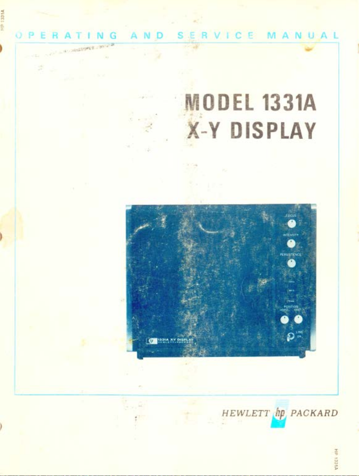
Page 1
~
U
PERATI
l\IG
.....
,.1,,;,·:··ffi''l.·1"
..
-..
:<
,
w·f'J'
i)i - - I
AND
7 '
.·
S E
RVIC
E
MANUAL
. - '
,.
ODEL
~.c.
L
•
i"".;;;
_,_..
-Y D
1331A
IS
PLAY
)
Page 2

CERTIFICATION
The He
wlett-Packard
thoroughly tested
specifications wh
Packard
ments
the
Company
are
extent
traceable to
allowed
WARRANTY
This
in
one
major
specified
prove
they
is
damages.
Hewlett-Packard
materials
year
components
to be
are
expressed
and
from
period.
defective
returned
or
and
en
Company
inspected
it
was
certifies that
and
found
shipped from
this
instrument
to
meet its published
the
factory. The Hewlett-
further certifies that its calibration measure-
the
U.S.
by
the
Bur
product
workmanship.
the
date
of
listed
We
will
during
to
Hewlett-Packard.
implied.
We
National
eau's
AND
delivery,
in
repair
calibration facility.
ASSISTANCE
is
the
operating
the
are
not
" '
Bur
eau
warranted
This
or
warranty
warranty
or,
in
replace
liable
the
No
for
of Standards
against
case
manual,
products
period
other
consequential
defects
applies
of
certain
for
provided
warranty
was
to
for
the
which
Service
available
tenance
For
any
Sales
back
and·S~rvice
of
contracts
for
Hewlett-Pa~kard
and
repair
assistance,
this
manual.
.
or
custoµier
on-site.
contact
Office.
assistance
products
your
nearest
Addresses
agreements
that
require
Hewlett-Packard
are
provided
are
main-
at
the
Page 3
(
OPERATING
Refer
to
Section
Refer
to
Section
standard
options: X95, 631.
AND
MODEL
X-V
SERIALS PREFIXED: 1319A
VI I for
VII
for
SERVICE
1331A
DISPLAY
instruments
instruments
with other
with
the
MANUAL
Serial Prefi
following
xes.
(
HEWLETT-PACKARD
1900
GARDEN
ManualPartNumber01331-90903.
MicrofichePartNumber01331-90803.
OF
THE GODS
COMPANY/COLORADO
ROAD, COLORADO
SPRINGS
SPRINGS
DIVISION
, CO
LORADO, U.S
.A.
PRINTED:
MAY
1973
Page 4
r
Table
of Contents
-·
Model 1331A
Section
I
GENERAL
1.
1-
4.
11-10.
1-1
1-14.
1-16.
1-20.
II
INSTALLATION.
2-1.
2-3
2-5
22-9.
2-11.
2-13.
2-17.
2-19.
2-34.
2-36.
III
OPERATION
3-1.
3-3.
3-5.
3
-7.
3-9.
3-11.
3-13.
3-
15.
IV
PRINCIPLES
4-1.
4-3.
4-5.
4-10. Secondary
12.
44-15
4-19
4-21.
4-23. Block
4-25.
4-27.
Description . . . . . . . . . . . . . . . . . . . . . .
Cathode-ray
2.
Warranty
Available
Instrument
Inquiries.
Introdu
.
Initial
.
Preparation
7.
Claims ........
Repacking
Introduction
Controls
Applications
Preoperational
Operator's
Operating
Introdu
Variable
.
.
INFORMATION
Introdu
ction . . . . . . . . . . . . . . . . . . . . . 1-1
Tube
....
....
Accessories.
and
Manu
Identifi
Rack
Power Requirements
Power
Instrument
Monitored
Amplifier
Beam
Intensity
Operator's
The
Erase
Variable
Storage
Storage
Low Voltage
High
cation
. . . . . . . . . . . . . . . . . .
........
. . .....................
ction
....................
Inspection
for
Use ...
Mounting
Connections
Cooling
Inputs
Input
...
for
Shipment
. . .
........................
.............
and
Connectors ........
Find ....
OF
OPERATION
ction
Persistence
Storage
Cycle
.......
Precautions
Diagram
Voltage Power
................
.....................
....................
Adjustments
Checks ...........
Maintenance ...
Procedur
....................
CRT
Emission
...................
Persistence . .
................
Discussion
Power
TABLE
........
................
............
al
..
..............
...............
...........
............
...........
...........
Modifications . .
..............
es
...........
and
.............
Ratio ...
...........
Supplies . . .
Supply
....
.... 1-1
. .
......... 1-1
........
..........
.......
..
........
. .
....
and
.. .. ..
Storage
........
.....
...
. . .
..
. . .
. .
. .
. .
. .
. . .
. .
P
age
. 1-1
1-1
1-1
1-1
1-3
2-1
.
2-1
.
2-1
2-1
.
2-1
2-1
.
.
2-1
.
2-1
2-1
2-2
2-5
.
2-5
.
3-1
3-1
.
3-1
.
3-1
3-1
.
3-2
3-
.
3
.
3-2
4-1
.
4-1
.
4-1
4-1
.
4-1
.
4-1
.
4-2
.
4-2
4-2
.
.
4
-2
4
-2
.
4-2
OF
CONTENTS
2
-2
Section
4-29.
4-31.
4-33.
4-35.
4-37.
4-54.
4-56.
4-64.
4-71.
4-76.
4-78
4-82.
v
PERFORMANCE
ADJUSTMENTS
5-
1.
5
-5.
5-8. Mode
5-
12.
5-
16.
5-2
0.
5-2
4.
5-28.
5-32.
6.
5-3
5-40.
5
-44.
5-47. Low
1.
5-5
5-55. Write Depth
5;5
9.
5-63.
5-67.
5-
71.
-75.
5
5-79. Store
5-83. Z-a
5-87.
5-89.
5
-91.
5-93.
X-
Z-axis Amplifier . . . . . . . . . . . . . . .
Intensity
Control
Pulse
Detailed
Low
High
X-
Z-
.
Control
Pulse
Introduction
Performance
Deflection
Phase
Common
Bandwidth
Z-axis Amplifier
Erase
Dot
Store
Adjustment
High
Flood
Write
X-
Phase
Writing
Calibrating
Instruments
Phase
Attenuator
Input
Page
and
Y-axis Amplifiers . . . . . . .
Gat
e . . . . . . . . . . . . . . . . .
Circuits................
Circuits
Circuit
Voltage
Voltag
and
Y-axis Amplifiers
axis
Amplifier . . . . . . . . . . . . . . .
Circuits.
and
Shift
(CMRR) Check . . . . . . . . . . . . . . . 5-2
Time
Writing
Time
Voltag
Adjustments
Voltage
Adjustment..
Gun and
Adjustments
Gun
Adjustment
and
Y-axis Amplifier
Adjustment
Shift
Time
xis
Amplifier Risetime
Adjustment.
Shift.
Signal
..
. . . . . . . . . . . . . . . .
Theory
Power
e Power
Circuits
. . . . . . . . . . . . . . . . .
CHECKS
. . . . . . . . . . . . . . . . . . . . . . 5
. . . . . . . . . . . . . . . . . . . . .
Check . . . . . . . . . . . . . . 5
Erase
Checks..........
Check
Mode Rejection
Checks
Check . . . . . . . . . . . . .
Time
Check . . . . . . . . . . 5-5/ 5-6
....
. .............
e Power
. . . . . . . . . . . . . . . . . 5-7
Power
Adjustment
Collimator
. . . . . . . . . . . . . . . . . 5
Intensity
. . . . . . . . . . . . . . . . . . 5
...............
Adjustment
Rate
Adjustment
Adjustment..
. . . . . . . . . . . . . . . . 5-10
Modified
. . . . . . . . . . . . . . . . . . 5-10
..................
Compensation.....
Amplitudes
. . . . . . . . . .
Supplies . . .
Supply
. . . . . . . . . . . . . . . .
AND
Checks.
. . . . . . . . . . . . . 5-2
. . . . . . . . . . . . . 5
Checks.
Check . . . . . . .
Supply
Supply
.............
Limit
. . .
.........
. . . . . . . 5-2
.... 5-2
Ratio
. . . . . . . 5
.... 5-7
..
. . . . . . . 5-7
Gain
.
. . . . . . . . 5-8
.......
. .
..... 5-9
. . . . . .
. 5-7
..
5-10
5-10
5-11
4-2
4-3
4-3
4-3
4-3
4-4
4-4
4-5
4-5
4-5
4-5
4-6
-1
5-1
5-4
5-4
-8
-8
5-8
5
-9
-1
-3
-3
11
Page 5
Model 1331A
Table
List
of
Contents
of
Illustrations
(
Section
VI
REPLACEABLE
6-1.
6-3.
VII
MANUAL
OPTIONS.........................
7-1.
7-3.
7-7.
7-11.
VIII
SCHEMATICS
SHOOTING
8-1.
8-3.
PARTS
Introduction
Ordering
Introduction
Manual
Special
Standard
Introduction
Schematics
Information
CHANGES
Changes
Options
Options
AND
.. .. .. . .. .. .. .. ..
TABLE OF
. . . . . . . . . . . . . . . . . . . . .
. . . . . . . . . . . .
AND
7-117-2
..
..
.
.
.
.
.. ..
7-117-2
"7-117-2
7-117-2
7-117-2
................
............
.............
...........
TROUBLE-
..
. . . . . . . . . . . . . . . . . . . . .
. . . . . . . . . . . . . . . . . . . . . .
CONTENTS
Page
6-1
6-1
6-1
8-1
8-1
8-1
(Cont'd}
Section
8-8.
8-12.
8-15.
8-17.
8-20.
8-23.
8-25.
8-27.
8-30.
8-32.
8-34.
8-36.
8-38.
8-40.
8-43.
8-45.
8-47.
Page
Reference
Component
Preventive
Mechanical
Cleaning....
Switch
Repair
CRT
Semiconductor
Circuit
Board
Servicing
Heat
Troubleshooting . . . . . . . . . . . . . . . . . 8-3
DC Voltages
Waveforms
Trouble
Designations
Locations
Maintenance
Inspection
...................
Maintenance
and
Replacement
Removal
Replacement.....
Boards
Connections.
Boards
Sinks...
and
Removal
. . . . . . . . . . . . . . . . . . . 8-3
Etched
.......................
..................
...................
.. .. .. ..
Isolation.
. . . . . . . . . .
............
. . . . . . . . .
. . . . . . . . .
. . . . . . . . . . . 8-2
. . . . . . . . . 8-2
Installation
and
............
. . . . . . . . . . . . 8-3
Circuit
.. . .. .. .. ..
. . . . . . . . . . . . . . 8-3
8-1
8-1
8-1
8-1
8-1
. 8-2
8-3
8-3
8-3
8-3
. 8-3
(
Figure
1-1.
1-2.
2-1.
2-2.
2-3.
2-4.
3-1.
3-2.
3-3.
3-4.
4-
1.
4-2.
4-3.
4
-4.
4-5.
4-6.
5-1.
5-2.
5-3.
5-4.
8-1.
8-2.
Title
Model 1331A
Instrument
Rack
Mounting
Ventilation
X-Y
Amplifiers
Attenuator
Main
Model 1331A
nectors
Preoperational
General Operating
Multiple
CRT
Schematic
Secondary
Erase
Cycle
Variable Persistence
Pulse
Circuits
Overall Block
Phase
Shift Trace
Erase
Waveform
Write
Depth
Adjustment
Al
Component
A2
Component
X-Y
Display
Serial
Number
.......................
Tolerances
Input
Components
Board
A5
.....................
Contro
.............................
Procedure
Procedure
Display
Procedure
.......................
Emission
...........................
Block
Diagram
.....................
......................
Waveform
Locator
Locator
Locator
.........
............
...............
Circuit
Locations
ls
and
Con-
..............
............
............
Ratio
Pulsing
Diagram
............
................
...............
................
................
LIST
..........
..........
..........
.........
OF ILLUSTRATIONS
Page
....
1-0
1-3
2-1
2-2
.
2-4
on
2-4
3-3
3-4
3-5
3-6
4-3
4-3
4-3
4-3
4-5
4-7
/ 4-8
5-3
5-4
5-7
5-11/5-12
8-4
8-5
Figure
8-3.
8-4.
8-5.
8-6.
8-
7.
8-8.
8-9.
8-10.
8-11.
8-12.
8-13.
8-14.
8-15.
8-16.
8-17.
8-
18.
8-19.
8-20.
8-2
1.
8-22.
Titl
e
Schematic,
Semiconductor
tification.
Schematic,
Supplies . . . . . . . . . . . . . . . . . . . . . . . . . . . . 8-7
A3
Component
Component
A4
Component
A 7
Schematic 3 Measurement
and
Schematic,
Supply
Schematic 4 Measurement
and
Schematic, X-and
Amplifiers . . . . . . . . . . . . . . . . . . . . . 8-11-8-12
Schematic 5 Measurement
and
Schematic
A6
Component
A8
Component
Schematic,
Component
A5
Schematic,
Write Mode Troubleshooting
Guide.........................
Store
Guide.
Erase
Guide..............................
±50
V Power Supplies 8-5
Terminal
. . . . . . . . . . . . . . . . . . . . . . . . . . . 8-7
+158V
and
Locator
Locator. . . . . . . . . . . . . . . . 8-8
Locator. . . . . . . . . . . . . . . . 8-8
Waveforms............
High
Voltage
..........................
Waveforms.
Waveforms...
, Z-axis Amplifier
Locator...............
Locator...............
Control Circuits . . . . . . . . . . 8-15
Locator
Pulse
Circuits
Mode
Troubleshooting
. . . . . . . . . . . . . . . . . . . . . . . . 8-21 /8-22
Function
Troubleshooting
Iden-
+12.6V
................
Power
..............
Y-axis
.................
...............
. . . . . . . 8-17 / 8-18
Power
Conditions
....
Conditions
8-1118-12
Conditions
.........
8-19/8-20
8-9/ 8-10
8-9/8-10
. 8-13
Page
8-8
8-13
8-14
8-15
8-16
8-23
111
Page 6
List
of
Tables
LIST
OF
TABLES
Model 1331A
Table
1-1.
1-2.
1-3.
2-1.
2-2.
2-
3.
3-1.
5-1.
5-2.
6-1.
6-2.
6-
3.
8-1.
Title
Specifications.........................
Accessories . . . . . . . . . . . . . . . . . . . . . . . . . . .
Reference
Abbreviations.......................
X-Y
Values............
Attenuator
Z-attenuator
Definitions............................
Recommended
Performance
Low
Adjustments
Abbreviations
Parts
Replaceable
List
Schematic
Designations
Attenuator
Voltage
List...........................
of
Manufacturer's
Component
Components
Component
Test
Equipment........
Check
Power
Parts
Notes......................
Record . . . . . . 5-6a/ 5-6b
Supply
. . . . . . . . . . . . . . . . . . . . . . . .
for
Replaceable
. . . . . . . . . . . . . . . . . . . . .
and
..................
Parts
List
Values
Codes....
. . . . 2-3
. . . . . . . 2-3
6-11
Page
1-2
1-3
1-3
2-3
3-1
5-1
5-7
6-1
6-2
/ 6-12
8-6
lV
)
Page 7

c
(
Page 8
Genera
l I
nformation
Model 1331A
)
1-0
Figure
1-1.
Model 1331A
X-Y
Display
1331A-A-7
)
Page 9
Model 1331A General
Information
(
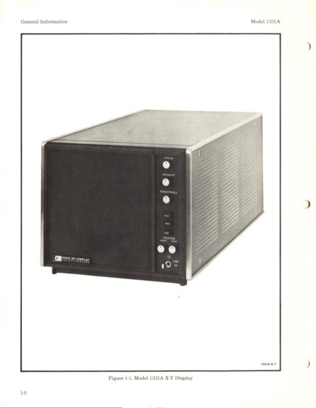
1-1. INTRODU CTION .
1-2.
This
manual
information
X-Y
Display (figure
eight
sections,
pect
of
the
instrument.
the
rear
of
used for reference while
manual.
1-3.
This
section
1331A.
table
viations used everywhere
Section VI.
puter
tions. Special accessories
Standard
listed
The
1-1.
Table
printout
options
and
described
provides
for
the
1-1).
each
covering a specific topic
the
manual
contains
instrument
1-3
The
parts
and
uses computer-supplied abbrevia-
available
in
Hewlett-Packard Model 1331A
The
All
and
reading
specifications
lists
and
in
list
are
Section
1-4. DESCRIPTION.
1-5.
Model 1331A
purpose
display
real time information.
makes
applications:
nuclear
swept-frequency
phase
tude
1-6.
monitor
fresh memory requirements
mesh
1
-7.
deflection
front
SISTENCE,
controls,
X-Y
digital
it
useful
spectrometer, semiconductor curve tracer,
shift
measurements,
versus
panel.
time
Identical X and
displays
type
storage
All
controls
and
These
mode (WRITE ,
and
has
storage
graphic
ERASE.
and
or
analog
as
a read-out device
measurements,
displays.
Y amplifiers provide
with
bandwidths
CRT.
required to
dot
writing
include
been designed for general-
system
computer-processed
Its
and
raster
FOCUS, INTENSITY,
operating
manual
schematics
can
a description
describes
this
in
Section VI
listed
for
VIL
high
alphanumeric
are
compensate
speed
and
STORE),
and
is
be unfolded
any
manual
in
this
instrument
monitoring.
frequency
in
frequency ratios,
displays, and
up
to 1 MHz. Re-
minimized
are
located on
SECTION
I
GENERAL INFORMATION
the
to
section for a description
servicing
1-10. CATHODE-RAY TUBE.
divided
are
part
are
this
the
into
or
lQcated
and
of
of
Model
listed
the
abbre-
except
is
a com-
section.
are
It
can
data
response
following
displays,
ampli-
storage
as-
at
the
in
in
or
1-11. Model 1331A uses a post-accelerator
CRT
with
inized P31
graticule
to
eliminate
used
eliminates
stantly
complete
1-12. WARRANTY.
1-13.
The
and
warranted
of
this
warranty.
form
is
the
CRT
warranty
return
returning
warranty
it
The
ments
tag.
1-14. AVAILABLE ACCESSORIES.
by
the
1-15.
Accessories
are
listed
for
spot
the
PER
POSITION
-
a wide
able for use
of
or request
Service Office.
range
other
paragraph
a 10.5 kV accelerating
phosphor.
is
located
refresh
CRT
instrument
manual.
The
located
fail
page, complete
with
a defective
page.
warranty
in
manufacturers.
information
on
available
of a suitable
The
on
the
parallax
specifications.
within
the
having a mutilated
table
of
with
errors.
the
need for memory devices to con-
the
display. Refer to
(except
as
stated
The
CRT
CRT
warranty
at
the
rear
the
time
the
defective CRT.
CRT
may
availab
test
HP
le for
1-2.
Hewlett-Packard also
equipment
instruments
Refer to
from
accessories
rack
potential
8 x 10 division
same
plane
as
The
mesh
type
table
the
CRT)
on
the
inside
is covered
of
specified on
warranty
is
described on
be
void for
use
the
the
by a separate
and
warranty
this
manual.
claim
The
procedure for
instru-
serial number
with
Model 1331A
and
accessories suit-
and
latest
nearest
in
this
adapter.
storage
and
alum-
internal
the
display
storage
1-1
for
is
certified
front
cover
claim
Shou
ld
the
CRT
form
and
the
CRT
has
instruments
HP
Catalog
HP
Sales
/
(
-8.
Model 1331A
1
which
blanking
is
shades
1-9. Model 1331A
ing
ments) side-by-side
adds a third
is
obtained
of
gray.
two
instruments
obtained
with
writes
+ 1 V. In-between voltages provide
is
and
stores
dimension
with-IV.
proportioned to
(any
in a standard
Maximum
HP
1330/ 1331-series instru-
shades
to
the
permit
19-inch rack. Refer
of
display.
brightness
mount-
gray
Spot
1-
16.
INSTRUMENT
TIFICATION.
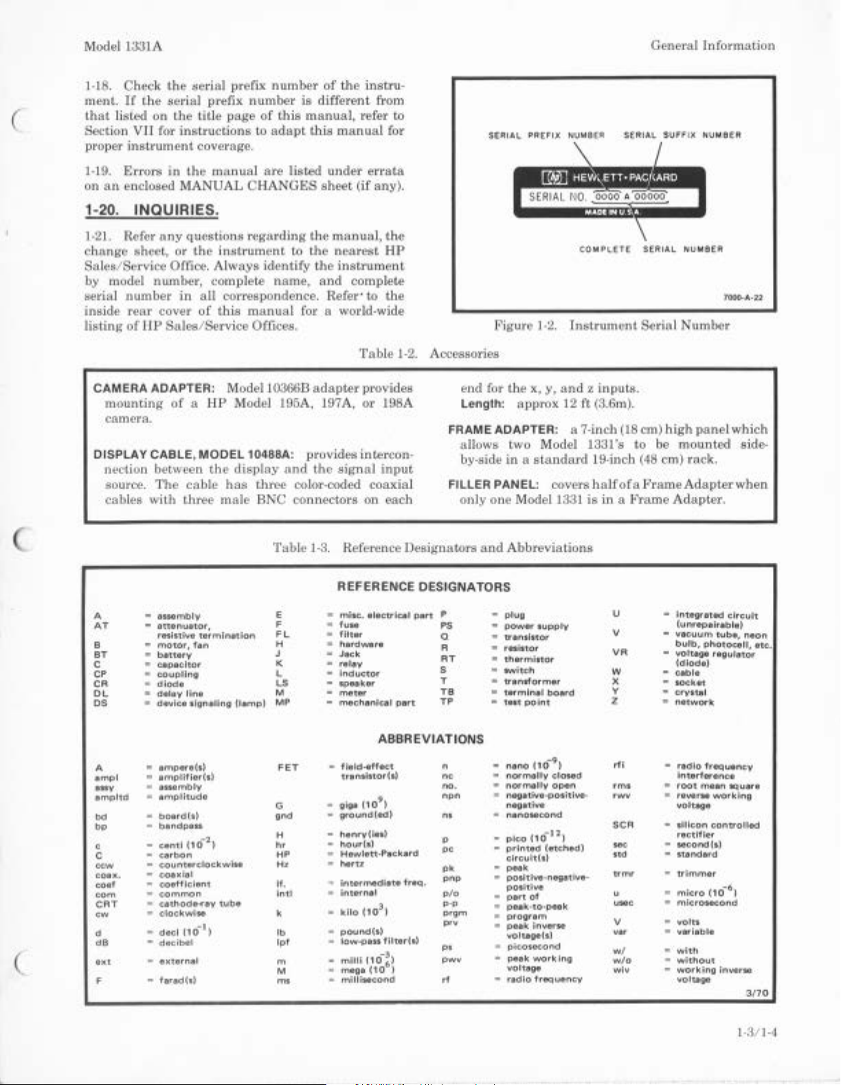
1-17.
This
manual
instruments
the
on
is
the
number
is
on a tag
manual
first
group
(figure
located
with a serial
title
of
1-2).
on
AND
applies
prefix
page. The
digits
in
The
instrument
the
rear
MANUAL
directly
number
serial
the
instrument
panel.
to
Model 1331
as
prefix
number
serial
number
IDEN-
listed
serial
1-1
Page 10
General
Information
Table
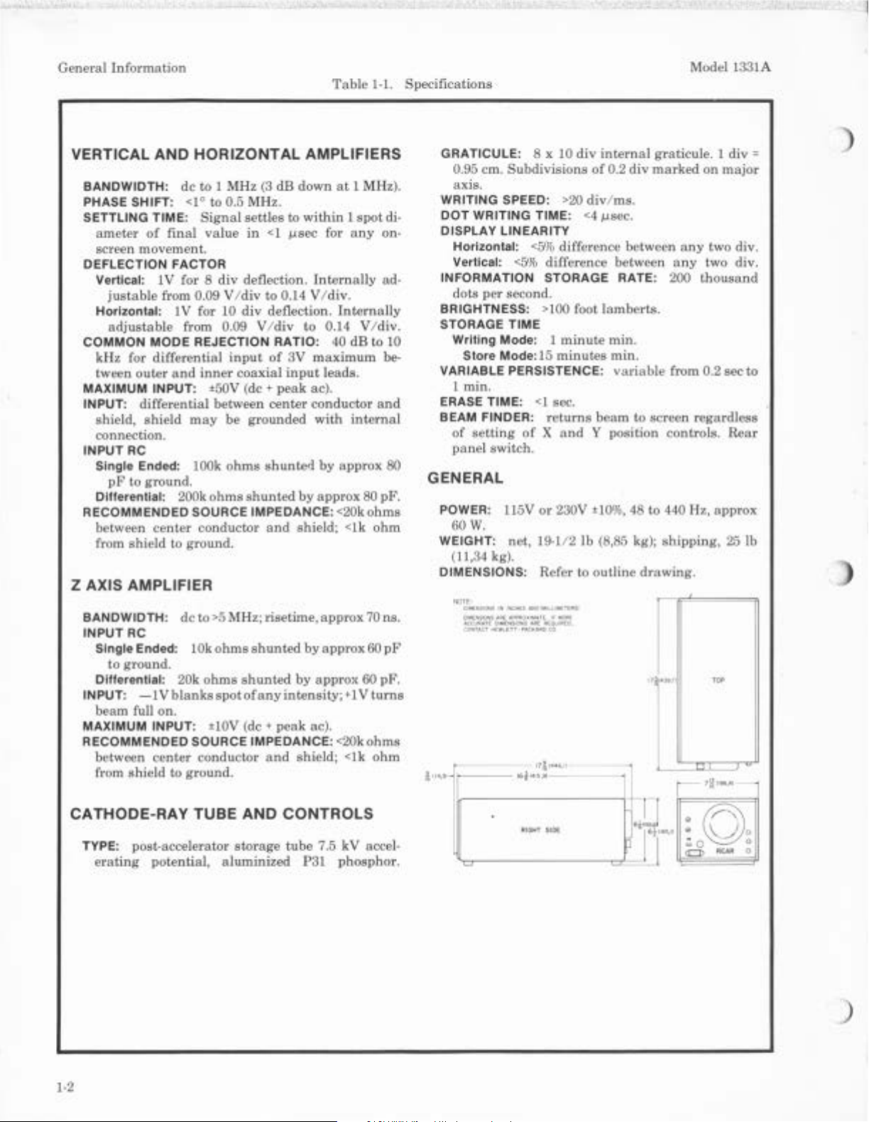
1-1. Specifications
Model 1331A
VERTICAL
BANDWIDTH:
PHASE SHIFT: <1° to 0.5 MHz.
SETTLING
ameter
screen movement.
DEFLECTION FACTOR
Vertlcal:
justable
Horizontal: 1 V for 10 div deflection.
adjustable
COMMON
kHz for
tween
MAXIMUM
INPUT:
shie
connection.
INPUT
Single Ended:
pF
Differential: 200k
RECOMMENDED SOURCE IMPEDANCE: <20ko
between center
from
AND
HORIZONTAL
de
to 1 MHz (3
TIME: Signal settles
of
final value
1 V
for 8 div
from 0.09 V /
from 0.09 V /
MODE
outer
differentia
ld,
shield
RC
to
ground.
shield
REJECTION RATIO: 40
differential
and
inn
INPUT: ±50V
l between
may
lOOk
ohms shunt
conductor
to
ground.
AMPLIFIERS
dB
down
at
to
within 1 spot
in
<1
µsec
for
deflection. Internally ad-
div
to 0.14 V / div.
Internally
div
to
0.14 V / div.
input
of
3V m
aximum
er
coaxial input lea
(de +
peak
ac).
center
conductor
be
gro
und
ed with
ohms shun
ed
and
ted
by
by
approx
shield; <
Z AXIS AMPLIFIER
BANDWIDTH: de
INPUT
IN
MAXIMUM
RECOMMENDED
RC
Single Ended: lOk
to
ground.
Differential: 20k
PUT:
-1
beam
full
INPUT:
between
from
shie
center
ld to
to
>5
MHz; risetime,
ohms
shunted
ohms shun
Vb
lanks
spot
on.
±lOV
SOURCE IMPEDANCE: <20k
conductor
ground.
of
any
(de +
and
ted
in
peak
approx
by
approx
by
approx
tensity;+ 1 V
ac).
shield;
1 MHz).
any
dB
to
ds.
internal
approx
80
lk
ohm
70 ns.
60
60
turns
ohms
<lk
ohm
di-
on-
10
be-
and
80
pF.
hms
pF
pF.
GRATICULE: 8 x 10
0.95 cm.
axis.
WRITING SPEED: >20
DOT WRITING
DISPLAY
Horizontal:
Vertical:
INFORMATION STORAGE
dots
BRIGHTNESS:
STORAGE
Writing Mode: 1
Store
VARIABLE
1 min.
ERASE
BEAM
of
panel
Subdivisions
LINEARITY
<5%
<5%
per
second.
TIME
Mode:15
PERSISTENCE:
TIME
: <l sec.
FINDER: returns
setting
of X and Y position
switch.
div
TIME:
difference
difference
>100
foot
minute
minutes
internal
of
0.2
div/ms.
<4
µsec.
between
RATE
lamb
min.
min
variable
beam
graticule. 1 div=
div
marked
between
erts.
.
to
any
any
: 200
from 0.2 sec to
screen
con
trols.
on
major
two div.
two div.
thousand
regardless
Rear
GENERAL
POWER
WEIGHT:
DIMENSIONS: Refer to
£11·.·-
: 115V
60W.
(11,34 kg).
NOTE1
DMC"'StONS
C>"'C~S
~ATE
OME...S10"fS
C
~TACT
HEvri.LCTT· PACKAAO
lo-
r-
--
-
-
or
230V
net,
19-112
I~
hCHES .6.ND().ILLY.ETfRS.I
ARC
APPRQX•VATE
"RE
~
-
,
6-,.:!··..
R£0v
lb
Jf
MORE
RCO
,
CO
±10%,
48
(8,85 kg);
outline
i I r
to
440 Hz,
shipping,
drawing.
approx
25
lb
TOP
,~
~1
CATHODE-RAY TUBE
TYPE: post-accelerator
era
ting
potentia
1-2
AND
CONTROLS
storage
l, aluminized P31
tube
7.5 kV acce
phosphor.
!..---
l-
'
\..J
RIGH
-T
SIOE---<
~
-
1Q""
LJ
J
~
Q
g~
<CJ)
REAR
0
Page 11
Model 1331A
General
Information
(
1-18.
ment.
that
listed
Section
proper
1-19.
on
an
Check
If
Errors
enclosed
the
the
serial
on
the
VII
for
instructions
instrument
in
MANUAL
serial
prefix
title
coverage.
the
manual
prefix
number
page
of
to
are
CHANGES
number
this
adapt
1-20. INQUIRIES.
1-21.
Refer
any
questions
change
Sales
by model
serial
inside
listing
sheet,
or
the
/ Service Office.
number,
number
rear
of
CAMERA ADAPTER: Model 10366B
mounting
cover
HP
in
all
of
Sales
/ Service Offices.
of a HP
camera.
DISPLAY CABLE,
MODEL
nection between
source.
cables
The
with
cable
three
regarding
instrument
Always
complete
identify
name,
correspondence.
this
manual
Model 195A, 197A,
10488A:
the
display
has
male
and
three
BNC
of
the
instru-
is
different
manual,
this
listed
the
to
the
the
manual
under
sheet
(if
manual,
nearest
instrument
and
complete
Refer·
refer to
errata
any).
to
for a world-wide
Table
adapter
provides
or
provides
the
color-coded
connectors
intercon-
signal
coaxial
on
from
for
the
HP
the
1-2. Accessories
198A
input
each
SERIAL
Figure
end
for
Length:
PREFIX NUMBER
1-2.
the
x, y,
approx
COMPLETE
Instrument
and z inputs.
12
ft
SERIAL
SERIAL
Serial
(3.6m).
FRAME ADAPTER: a 7-inch (18 cm)
allows
by-side
FILLER PANEL: covers
only
two
Model 1331's to be
in a standard
one
Model 1331
19-inch (48
halfofa
is
in a Frame
Frame
SUFFIX
NUMBER
Number
high
mounted
cm)
rack.
Adapter
Adapter.
NUMBER
panel
7000-A-22
which
side-
when
(
A
AT
B
BT
c
CP
CR
DL
OS
A
amp
assy
amp
bd
bp
c
c
ccw
coax.
coef
com
CRT
cw
d
dB
ext
F
I
ltd
assembly
attenuator,
resistive
motor,
battery
capacitor
coupling
diode
delay
device
termination
fan
line
signaling
ampere(s)
amplifier(s)
assembly
amplitude
board(s)
bandpass
(10
coefficient
clockwise
-I
(10
external
farad(s)
-2
)
tube
)
centl
carbon
counterclockwise
coaxial
common
cathode..-ey
decl
decibel
(lamp)
Table
1-3. Reference
E
F
FL
H
J
K
L
LS
M =
MP
FET
G
gnd
H
hr
HP
Hz
If.
inti
k
lb
lpf
m
M
ms
Designators
REFERENCE DESIGNATORS
misc.
electrical
fuse
filter
hardware
Jack
relay
=
inductor
speaker
meter
mechanical
field-effect
transistor(s)
giga
(10
ground(ed)
henry(ies)
hour(s)
Hewlett-Packard
hertz
intermediate
internal
kilo
(10
pound(s)
low-pass
mllli
(10
mega
(10
millisecond
part
ABBREVIATIONS
9
)
3
)
filter(s)
-3
)
6
)
part
freq.
p
PS
Q
A
RT
s
T
TB
TP
n
nc
no.
npn
ns
p
pc
pk
pnp
p/o
p-p
prgm
prv
PS
pwv
rf
and
Abbreviations
plug
=
power
transistor
resistor
=
thermistor
=
switch
transformer
terminal
=
test
point
nano
normally
normally
negative-positivenegative
nanosecond
pico
(10
printed
circuit(s)
peak
positive-negativepositive
part
of
peak-to-peak
program
=
peak
voltage(s)
picosecond
peak
voltage
=
radio
supply
board
9
)
(1
o-
closed
open
-12
)
(etched)
inverse
working
frequency
u
v
VA
w
x
y
z
rfl
rms
rwv
SCA
sec
std
trmr
u
usec
v
var
w/
w/o
wiv
Integrated
(unrepairable)
-
vacuum
bulb,
voltage
(diode)
=
cable
socket
=
crystal
network
=
radio
interference
root
mean
reverse
voltage
=
silicon
rectifier
second(s)
standard
trimmer
micro
microsecond
volts
variable
with
without
working
voltage
circuit
tube,
photocell,
regulator
frequency
square
working
controlled
-6
(10
)
inverse
neon
etc.
3/70
1-
3/ 1-4
Page 12

(
Page 13
Model 1331A
Installation
(
2-1.
INTRODUCTION.
2-2.
This
section
an ini
tial
procedures
by-step order.
warranty
for
repairs
shipment
conta
inspection
and
precautions
The
procedures for making
and
are
also
ins
instructions
of
Model 1331A.
are
for
repacking
described
presented
in
this
2-3. INITIAL INSPECTION.
2-4.
The
instrument
electrically before
it
for
damage
Check for broken knobs,
and
dents
or
scratc
the
claims
packing
paragraph
material
shipment.
that
hes.
for
was
inspected
may
hav
bent
If
damage
in
this
possible
mechanically
Upon
e occurred
or
broken
is
section.
future
use.
2-5. PREPARATION FOR USE.
2-6.
Model 1331A
for use
listed
other
instrument.
as a bench
in
Section
mechanical
is
shipped
instrument
I.
The
following
and
electrical
from
the
with
specifications
paragraphs
configurations
INSTALLATION
for
performing
Installation
in
step-
a c
laim
the
insltument
section.
and
receipt,
found, refer to
inspect
in
transit.
connectors,
Retain
factory
discuss
ready
of
SECTION
for
the
as
the
II
2-9. POWER REQUIREMENTS.
2-10.
Model 1331A
230 Vac
shipped
fically ordered for 230
one
to
fuse
fuse size is
2-11. POWER CONNECTIONS.
2-12.
ment
is
equipped
when
the
and
Electrotechnical
To
from a two-contact outlet,
two-conductor
ground
2-13. INSTRUMENT
±10%,
ready
voltage
the
in
instrument
mating
preserve
to
voltage
the
fuseholder
indicated
Hewlett-Packard
panel
and
with
connected to
plug
this
at
the
power outlet.
operates
48 to 440 Hz. All
for 115
the
desired
cabinet
a three-conductor power
through
of
Commission
adapter.
Vac
Vac
operation. To
other,
set
and
on
above
recommends
be
an
appropriate
the
the
power cord
protection
Connect
COOLING.
operation
the
install
the
the
grounded. Model 1331A
offset pin.
(IEC)
feature
use
on
either
SELECTOR
rear
fuseholder.
receptacle,
meet
a three-conductor to
the
115
instruments
unless
change
the
appropriate
panel.
that
tlie
cab
grounds
The
power
International
safety
when
adapter
standards.
operating
Vac
spec
from
switch
Correct
instru-
le
that,
wire to
or
are
i-
jack
(
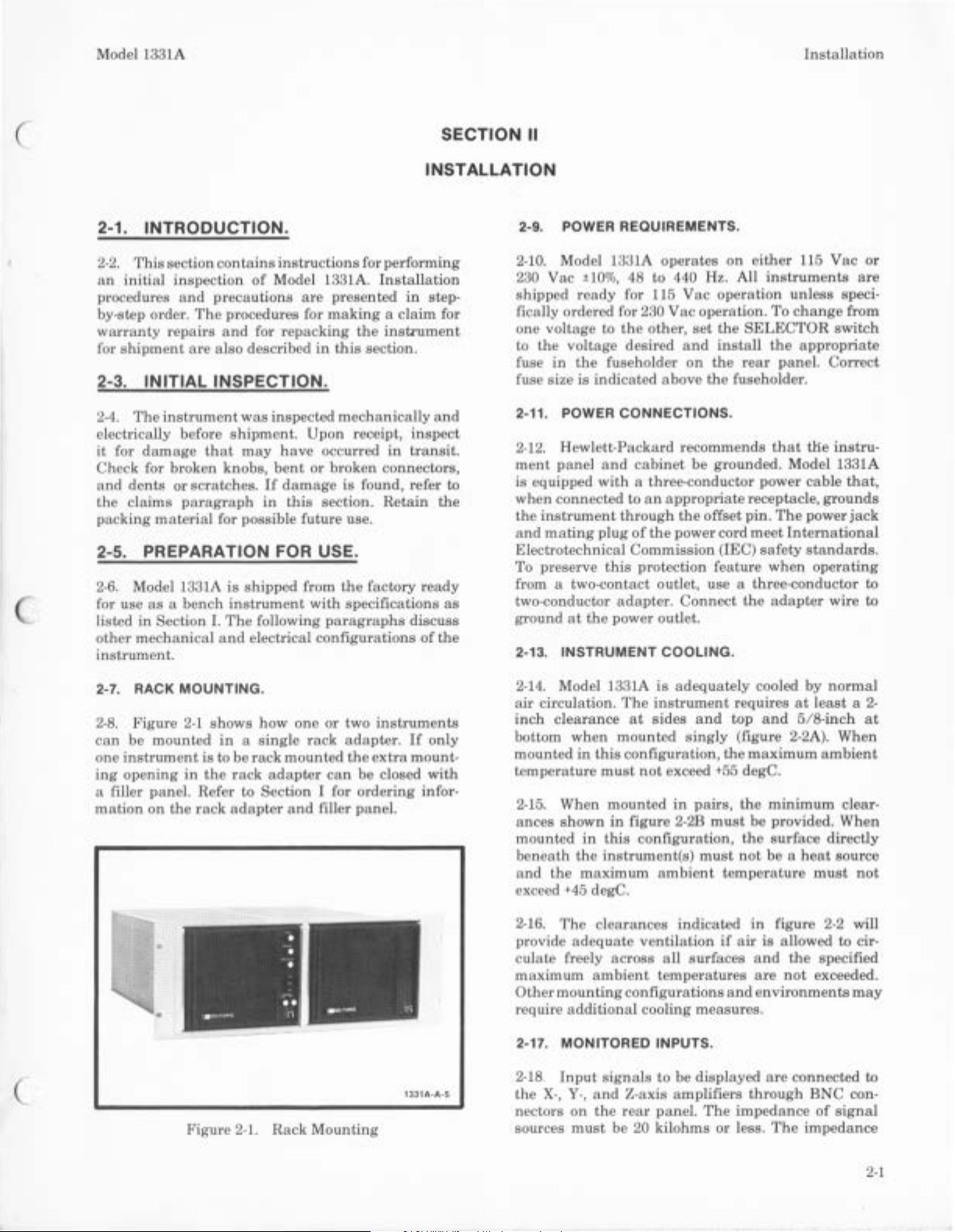
2-7. RACK
2-8.
can
be
one
instrument
ing
opening
a filler panel. Refer
mation
Figure
mounted
on
MOUNTING
2-1
shows
in a single
is to
in
the
the
rack
•
Figure 2-
.
how
be
rack
rack
adapter
to
Section I for
adapter
1.
Rack
one
or
rack
mounted
can
and
filler panel.
Mounting
two
instruments
adapter.
the
extra
be
closed
ordering
If
only
mount-
with
infor-
1331A·A·S
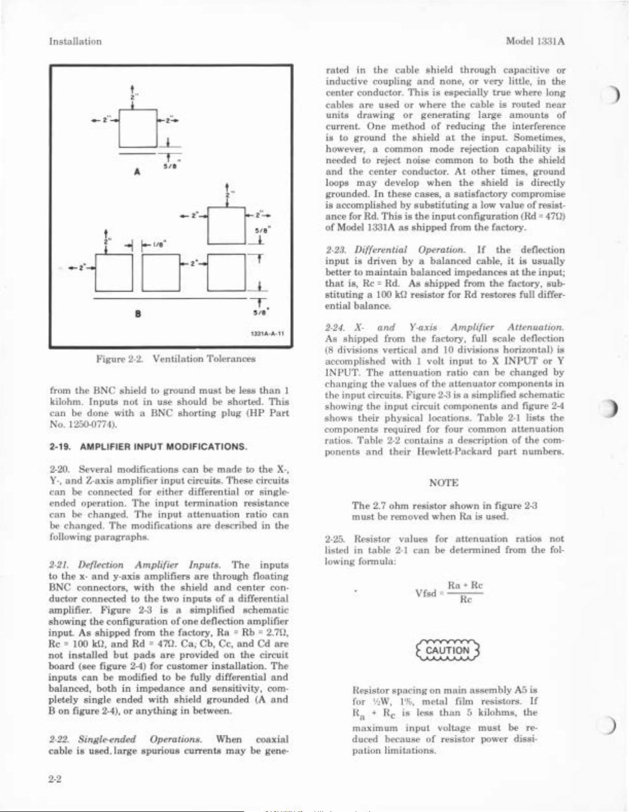
2-14.
Model 1331A
air
circulation.
inch
clearance
bottom
mounted
temperature
2-15.
ances
mounted
beneath
and
exceed
2-16.
provide
culate
maximum
Other
require
2-17. MONITORED INPUTS.
2-18
the
nectors
sources
when
in
this
must
When
mount
shown
in
this
the
instrument(s)
the
maximum
+45
degC.
The
clearances
adequate
freely
ambient
mounting configurations
additional
Input
signals
X-,
Y-,
and
on
the
must
The
instrument
at
sides
mounted
configurat
not
ed
in
figure
configurat
ventilation
across
coo
Z-axis
rear
be
20 kilohms
is
adequately
and
singly
ion,
exceed
in
pairs,
2-2B
must
ambient
indicated
all
surfaces and
temperatures
ling
measures.
to
be
displayed
amp
panel.
cooled
requires
top
(figure 2-2A).
the
maximum
+55
degC.
the
must
be
ion,
the
not
temperature
in
if
air
are
and
environments
lifi
ers
through
The
impedance
or
less.
by
normal
at
least a 2-
and
5/ 8-inch
minimum
provided.
surface
be a heat
must
figure 2-2 will
is allowed to cir-
the
not
exceeded.
are
connected to
BNC
of
The
impedanc
at
When
ambient
clear-
When
directly
source
not
specified
may
con-
signal
e
2-1
Page 14
Installation
rated
in
the
inductive
center
cables
units
current.
is
to
however, a
coupling
conductor.
are
used
drawing
One
method
ground
common
the
needed to reject
and
the
center
loops
grounded.
is
ance
of
may
develop
In
these
accomplished
for Rd.
This
Model 1331A
cable
shield
and
This
or
where
or
generating
shield
noise
conductor.
when
cases, a
by
substituting
is
the
as
shipped
none,
is
especially
the
of
reducing
at
mode
common
At
satisfactory
input
from
Model 1331A
through
or
capacitive
very
little,
true
cable
is
the
input.
both
times,
routed
amounts
interference
capability
large
the
rejection
to
other
the
shield
compromise
a low
value
configuration
the
factory.
or
in
the
where
long
near
of
Sometimes,
is
the
shield
ground
is
directly
of
resist-
(Rd=
47Q)
B
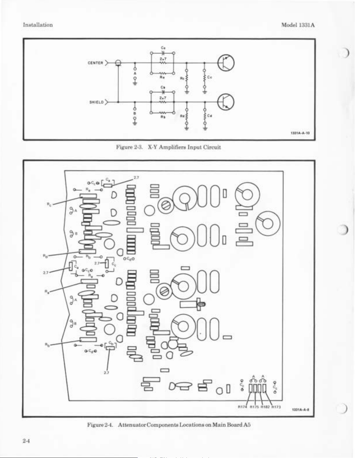
Figure
from
the
BNC shield to
kilohm.
can
No
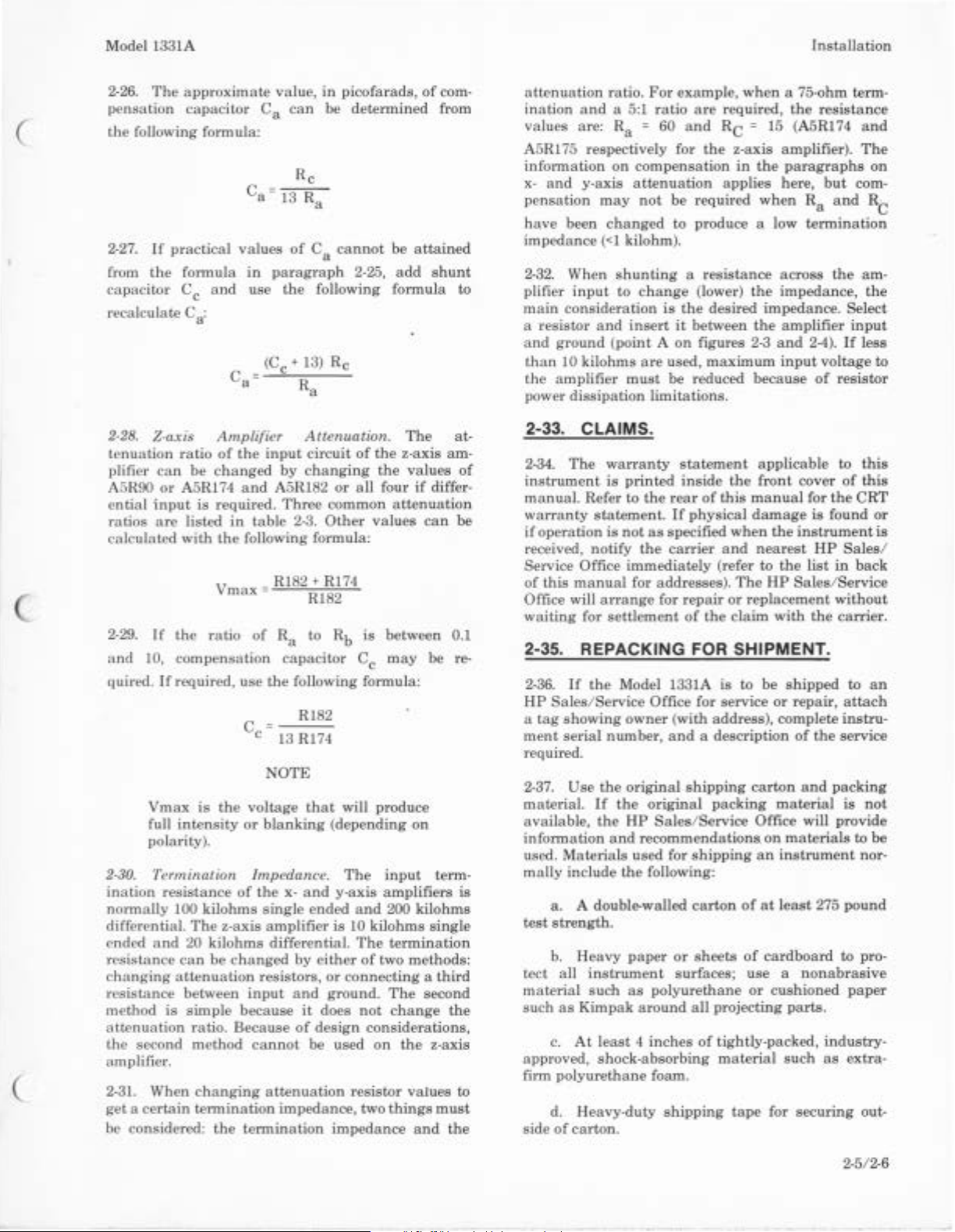
2-19. AMPLIFIER INPUT MODIFICATIONS.
2-20.
Y-,
can
Inputs
be
done
. 1250
-077
Several
and
Z-axis
be connected for
ended operation.
can
be
changed. The
be
changed.
following
2-21.
to
the x-and
paragraphs.
Deflection
BNC connectors,
ductor connected to
amplifier.
showing
input.
Re=
not
board
inputs
balanced,
pletely
B
on
2-22.
cable
the
As
shipped
100
kn,
installed
(see figure
can
both
single
figure 2-4),
Single-ended Operations. When coaxial
is
used,
2-2.
Ventilation
not
in
use
with a BNC
4).
modifications
amplifier
input
either
The
input
input
The
modifications
Amplifier
y-axis amplifiers
with
the
the
Figure
2-3
is
configuration
from
the
and Rd= 47n.
but
pads
are
2-4)
for customer
be
modified to
in
impedance
ended
large
or
anything
spurious
with
ground
must
should
shorting
can
be m
circuits.
differential
termination
attenuation
are
Inputs.
are
shield
two
inputs
a simplified
of
one
deflection amplifier
factory,
Ca;
Cb, Cc,
provided
be
fully
and
shield
in
between.
currents
Tolerances
be less
be
shorted.
plug
ade
These
described
The
through
and
center
of
a differential
Ra =Rb
and
on
installation.
differential
sensitivity,
grounded
may
T.
5111
1331A
-A-1
than
This
(HP
Part
to
the
circuits
or
single-
resistance
ratio
can
in
the
inputs
floating
con-
schematic
= 2.7n,
Cd
are
the
circuit
The
and
com-
(A
and
be
gene-
1
X-,
2-23. Differential Operation.
input
is
driven
better
to
maintain
that
is,
Re=
stituting
ential
2-24.
As
(8
a 100
balance.
X.
shipped
divisions
accomplished
INPUT.
1
changing
the
showing
shows
input
their
The
the
circuits.
the
components
ratios.
ponents
Table
and
by a balanced
balanced
Rd. As
kn
resistor
and
from
Y-axis
the
vertical
with 1 volt
attenuation
values
Figure
input
circuit
physical
required
2-2
contains
their
shipped
factory, full
and
10
of
the
2-3 is a simplified
components
locations.
for
four
Hewlett-Packard
If
the
cable,
impedances
from
the
for
Rd
restores full differ-
Amplifier
sca
divisions
input
to X
ratio
can
be
attenuator
components
Table
common
a description
part
deflection
it
is
usually
at
the
input;
factory, sub-
Attenuation
le deflection
horizontal)
INPUT
or
changed
schematic
and
figure
2-1
lists
attenuation
of
the
com-
numbers
.
is
Y
by
in
2-4
the
.
NOTE
The
2. 7
ohm
must
2-25.
Resistor
listed in
be
removed
values
table 2-1
resistor
can
shown
when
Ra
for
attenuation
be
determined
is
in
used.
figure 2-3
ratios
from
the
not
fol-
lowing formula:
Ra+
Re
Vfsd
= Re
Resistor
for 1/i
Ra + Re
maximum
duced b
pation
spacing
W, 1%,
is
metal
less
input
eca
use
limitations.
on
main
film resistors.
than
voltage
of
resistor
assembly
5 kilohms,
must
be
power dissi-
A5
is
If
the
re-
2-2
Page 15
Model
1331A
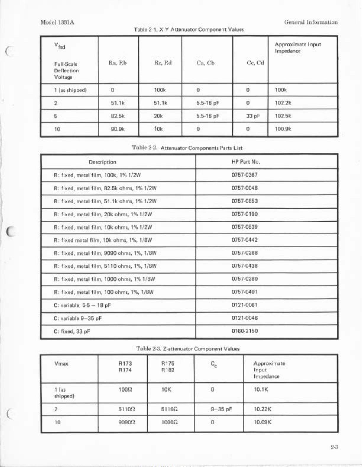
Table 2-1.
X-Y
Attenuator
Component
Values
General Informat
ion
(
vfsd
Re,
Full-Scale
R
a,
Rb
Rd
Ca,
Cb
Deflection
Voltage
1 (as shipped) 0 100k 0 0
2
5
10
51.1k
82.5k
90.
Description
R:
fixed, metal film, 100k,
R:
fixed, metal film, 82.5k
R:
fixed, metal film, 51.1k ohms,
R:
fixed, metal film, 20k
ohms,
9k
1%
1/2W
ohms,
Table
1%
1%
1% 1/2W
51.1
k 5.5-18 pF
20k 5.5-18
f
Ok
2-2.
Attenuator
1/2W
1/2W
pF
0 0
Components
Par
ts
List
HP
Part No.
0757-0367
0757-0048
0757-0853
0757-0190
Approximate
Impedance
Cc,
Cd
100k
0
33 pF 102.5k
102.2k
100.9k
Input
R: fixed, metal film, 10k
R:
fixed metal film, 10k
R:
fixed, metal film, 9090
R:
fixed, metal film , 5110
R:
fixed, metal film, 1000
R:
fixed, metal film, 100
C:
variable,
C:
variable
C:
fixed, 33 pF
5-5
9-35
- 18 pF
pF
ohms,
ohms,
ohms,
ohms,
ohms,
ohms,
1% 1/2W
1%,
1/8W
1%, 1/8W
1%,
1/
1%
1/8W
1%,
1/8W
Table
8W
2-3.
Z-attenuator
Vmax R173 R175
R174 R182
1 (as
1oon
10K
shipped)
Component
cc
0
0757-0839
0757-0442
0757-0288
0757-0438
0757-0280
0757-0401
0121-0061
0121-0046
0160-2150
Values
Approximate
Input
Impedance
10.
lK
2
10
5110Q 5110Q
9090Q
1ooon
9-35
pF 10.22K
0
10.
09K
2-3
Page 16
Installation
Ca
Model 1
33
1A
~
dA
CENTER
SHIELD
C>
Cc
E>~
8
R
--0
A
i
B
i
Figure
c 2.7
D
D
2-3.
~
CJ
X-Y
2.1
Ra
C•
2.7
Rb
Amplifie
Re
Rd
-=
rs
Input Circuit
Cc
Cd
1331A-A-10
"'~--;JJ
':
.-t:~~~~
:i
·?
~
·
~?~~
~
~,,~t
~
2.7
Figure
2-4.
o"o
,
o~
§~00
~o=~
l2a
Attenuator
!=
~:o
Components
00=
Locations on
Main
Board
A5
1331A-A-8
)
2
-4
Page 17
(
Model 1331A
2-26.
The
approximate
pensation
the
following formula:
2-27.
from
capacitor
recalculate
If
practical
the
Cc
capacitor
formula
Ca:
value,
Ca
can
values
and
of
in
par
agrap
use the following
in
picofarads,
be
ca
cannot
h 2-25,
determined
be
attained
add
formula
of
com-
from
shunt
to
attenuation
ination
values are:
A5Rl
information
x-
and
pensation
have
impedance (<l kilohm
2-32.
plifier
main
a
resistor and
and
ground
than
the
amplifier
power dissip
ratio.
For
and
a 5:1
ratio
Ra = 60 and
75 respectively
on
compensation
y-axis
been
When
input
consideration
10
kilohms
attenuation
may
not
changed
shunting a resistance
to
change
insert
(point
are
must
ation
limitations.
example,
are
required,
Re
for
the
z-axis amplifier).
applies here,
be
required
to
produ
ce a low
).
(lower)
is
the
desired
it
between
A on figures
used,
maximum
be
reduced
when
a 75-ohm term-
the
= 15
(A5Rl
in
the
paragraphs
when
across
the
impedance, the
impedance
the
amplifier
2-3
and
input
because
Installation
resistance
74
and
The
on
but
com-
Ra
and
RC
termination
the
am-
. Select
input
2-4).
If
less
voltage
of
to
resistor
(
2-28.
Z-axis
tenuation
plifier can
A5R90
ential input
ratios
calculated
2-29.
and
quired.
2-30.
ination
normally
differential.
ended
resistance
changing
resistance
method
attenuation
the
amp
2-31.
get a certain
be considered:
ratio
be
or
A5R l
are
listed
with
If
the
10,
compensation
If
required,
Vmax
intensity
full
polarity).
Termination
resistance
100
The z-axis
and
20
can
attenuation
between
is
simple
ratio. Because
second
lifier.
method cannot
When
changing
termination
Amplifier
of
the
input
changed
74
and
is required.
in
table
the
following formula:
_
V
max
-
ratio
of
use
c =
c 13
NOTE
is
the
voltage
or
blanking
imp
of
the x-and
kilohms
kilohms
be
the
single
amp
changed
resistors,
input
because
attenuation
termination
Attenuation.
circuit
by
changing
A5Rl82
Three
2-3.
Rl82
Rl82
Ra
to
capacitor
the
following formula:
Rl82
---
Rl74
that
edance.
lifi
differential.
by eith
and
it
of
impedance,
of
or
all four
common
Other
+ R174
Rb
Cc
will produce
(depending
The
y-axis amplifiers
ended
and
er
is
10
The
er
or
conn
ground.
does
not change the
design
be used
resistor
impedance
The
the
z-axis am-
the
values
if
differ-
attenuation
values
is between 0.1
kilohms
of
considerations,
on
two
can
may
be re-
on
input
200
two methods:
ecting a third
The
things
term-
kilohms
single
termination
second
the
z-axis
values
must
and
the
at-
of
be
is
to
2-33. CLAIMS.
2-34.
The
warranty
instrument
manual.
warranty
if
operation
received,
Service Office
of
this
Office will
waiting
is
Refer to
statement.
is
notify
manual
arrange
for
settlement
printed
not
immediately
statement
inside
the
rear
of
this
If
physical
as
specified
the
carrier
for addresses).
for
repair
of
the
(refer to
and nearest
applicable
the
front
manual
damage
when
the
the
The
HP
or
replacement
claim
with
cover
for
is found
instrument
HP
list
Sales
the
2-35. REPACKING FOR SHIPMENT.
2-36.
If
the
Model 1331A
HP
Sales
/ Service Office for service
a
tag
showing
ment
serial
required.
2-37.
Use
material.
ava
ilable,
information
u
se
d.
Materials
mally
include
a.
A double-walled
test
strength.
b.
Heavy
tect
all
material
such
as
c.
At
approved, shock-absorbing m
firm
polyurethane
d. Heavy-duty
side
of
carton.
owner
number, and
the
original
If
the
original
the
HP
and
recommendations.
used
the
following:
paper
instrument
such
as
Kimp
ak around
least 4 inches
(with address), complete
Sales
for
or
polyurethane
foam.
shipping
is
to
be
shipped
or
repair,
a description
shipping
packing
/Service Office will provide
shipping
carton
sheets
surfaces;
all
of
of
use a nonabrasive
projecting
of
tightly-packed,
ate
tape
of
carton
material
on
materials
an
instrument
at
least
cardboard
or
cushioned
parts.
rial
such
for
securing
the
and
275
to
this
of
this
the
CRT
Sales
in
back
/ Service
without
carrier.
to
an
attach
instru-
service
packing
is
not
to be
nor-
pound
to
pro-
paper
industry-
as
extra-
out-
or
is
/
2-5
/ 2-6
Page 18

(
Page 19
Model 1331A
Operation
(
3-1.
3-2.
1331A op
tor
opera
words a
of
INTRODUCTION
This
section
era
ting
's
checks
ting
the
instrument.
and
instructions.
nd
phr
ases
contains
controls,
adjustments, and
Table
used
3-3. CONTROLS AND
3-4.
All co
ntrols
described
expl
3-5. BEAM FIND.
3-6.
to locate
due
POSITION
the
BEAM
in
anatio
n are covered
The BEAM
the beam
to
a large
FIND
and
figure 3-1.
FIND
input
controls,
cont
connectors
Controls
in
cont
when
voltage,
or a malfunction.
rol,
pro
.
an
explanation
mod
es
of
operation, opera-
step-by-step
3-1 co
ntains a list
to d
escr
ibe
the
CONNECTORS.
are
identified a
requiring
the
following
rol is a sli
it
is deflected
misadjustment
ceed
as
follows:
para
de
switch used
off
To
SECTION
OPERATION
of
Model
of
operation
nd
further
gra
phs.
screen
of
the
operate
111
Set
a.
b.
c.
visible.
d. D
to vie
e.
n
ot
operate corr
3-7. INTENSITY.
INTENSITY
Set
BEAM
Turn
ete
wing
area.
Set
A
high
period
the CRT
INTENSITY
rmine action
BEAM
inten
of
time
display
FIND
ectly
sity
FIND
with
display
can cau
area.
fully ccw.
to ON.
slowly cw
required to
to off. Model 1331A will
BEAM
over
se
burn
until
return
FIND
an
extended
damage
set
beam
beam
to ON.
to
is
Word
or
Phrase
Write
Persistence
Store
Erase
Int
ens
ity
Bloom
Backgro
illumination
Fade
und
positive
Table
3-1.
Definitions
To
display
The length
C
RT
moved
To
a
display
To
been
The
CRT.
Visible,
tortion
A light-green
tire
An increase
tens
transform
on
the
of
after
the
.
retain
, for
that
remove all
written
brightness
nonsymmetric
of a display
CRT
viewing
ity
occuring
Definition
an
input
CRT.
time a displ
writing
an
extended
has
been
displays
or
sto
red
of
a displ
written
illumination
area.
in
background
in eith
signal
signal has been re-
written
and
on the CRT.
ay
al
expansion
er
write
into a visua
ay
remains
period
of
on the CRT.
blooms that
written
on
the
CRT.
cove
ring
illumination
or
store
on
tim
e,
on the
and
the
en-
mode.
l
the
have
dis-
in-
(
Fade
negative
A decrease
or
write
sto
in
re
trace
mode.
int
ensity
occuring
in eith
er
3-1
Page 20
Operation
Model 1331A
3-8.
The
INTENSITY
tens
ity from completely
ness
(cw)
in the
CRT, follow
3
-2
before
slowly
vie
wing
the
operating
until the
level
without
display
control
off
(ccw) to
write
mode. To
preoperational
the
instrument. Increase
brightness
blooming.
adjusts
maximum
avoid
procedure
is
at
the
display
damage
in
intensity
a comfortable
3-9. APPLICATIONS.
3-10. Model 1331A
of
x-,
y-,
and z-axis
and
sensitivity
in
Section I).
ferential
:
md
modified (Section
many
paragraph
cations.
or
single
amplifier
specific
in
can
be
used for
displays
specifications (refer
Furthermore,
ended),
input
termination
II)
to
applications.
Section I
the
amplifier
meet
Refer to
for
a l
within
ist
any
application
its
bandwidth
to
specifications
type
of
input
deflection factor,
impedance
the
requirements
the
description
of suggested
3-11. PREOPERATION ADJUSTMENTS
OPERATOR 'S CHECKS.
3-
12.
The
preoperational
figure 3-2.
check to verify
This
procedure
proper
procedure is
also
serves
operation
of
shown
as
an
the
instrument.
operator
in-
bright-
to
the
figure
(dif-
can
be
app
AND
of
li-
in
3-13.
3
-14.
limited to
and
on
This
surfaces
with
can
detergent.
OPERA
Operator's
the
exterior
the
exposes
a commercial
be removed
cleaning
contrast
the
and
smooth
TOR'S
maintenance
ope
rator
's
of
screen
face
of
metal
glass
with a mi
MAINT
checks
the
instrument.
for
removal
the
CRT
surfaces
cleaner.
ENANCE.
of
Model 1331A is
in
paragraph
Pull
and
for cleaning.
can
Stubborn
ld liquid
3-15. OPERATING PROCEDURES.
3-16. Fi
operating
photographs
instructions.
explained
be modified
unique
gures
3-2
procedures.
correspond
Only
in
the
or
operating
through
the
illustrations.
combined to fill a
requirements.
The
basic
3-4
contain
index
to
step
operating
These
step-by-step
numbers
numbers
techniques
techniques
wide
3-12
upward
cleaning.
Glass
be
cleaned
residues
household
on
the
in
the
are
can
variety
of
3-2
Page 21
Model 1331A
Operation
(
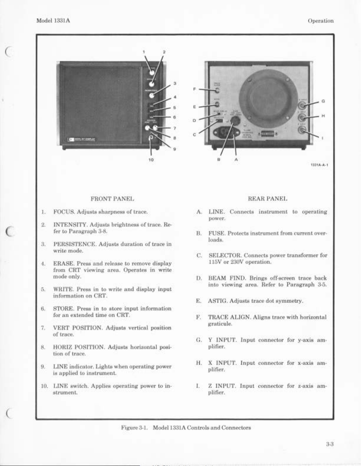
1.
FOCUS.
2.
INTENSITY.
Paragraph
fer to
PERSISTENCE.
3.
write mode.
4.
ERASE.
from
CRT
mode only.
5. WRITE.
information
6. STORE.
for
an
extended
7.
VERT
of
trace.
8.
HORIZ
tion
of
9.
LINE
indicator.
is
applied
FRONT
Adjusts
Press
Press
Press
POSITION.
POSITION.
trace.
to
sharpness
Adjusts
3-8.
and
viewing
in
on
CRT.
in
time
Lights
instrument.
PANEL
brightness
Adjusts
release
area.
to
write
to
store
on
Adjusts
Adjusts
when
of
duration
to remove
Operates
and
input
CRT.
vertical
horizontal
operating
10
trace.
of
trace. Re-
of
trace
display
in
display
information
position
2
in
write
input
posi-
power
B A
REAR
A.
LINE.
power.
B.
FUSE. Protects
loads.
C.
SELECTOR.
115V
D. BEAM
into
E. ASTIG.
F. TRACE ALIGN.
graticule.
G. Y
plifier.
X
H.
plifier.
Connects
or
230V operation.
FIND.
viewing
Adjusts
INPUT.
INPUT.
Connects
area.
Input
Input
PANEL
instrument
instrument
power
Brings
trace
off-screen
Refer to
dot
Aligns
connector
connector
trace
to
from
current
transformer
trace
Paragraph
symmetry.
with
horizontal
for
y-axis
for x-axis
1331A-A-1
operating
over-
for
back
3-5.
am-
am-
(
10.
LINE
switch. Applies
strument.
operating
Figure
power to in-
3-1.
Model 1331A
I.
Controls
Z
INPUT.
plifier.
and
Input
Connectors
connector
for z-ax1s
am-
3-3
Page 22
Operation
11,
13
1,
3
6,8
7,
2
Model 1331A
4,
5
8
1331A-A-2
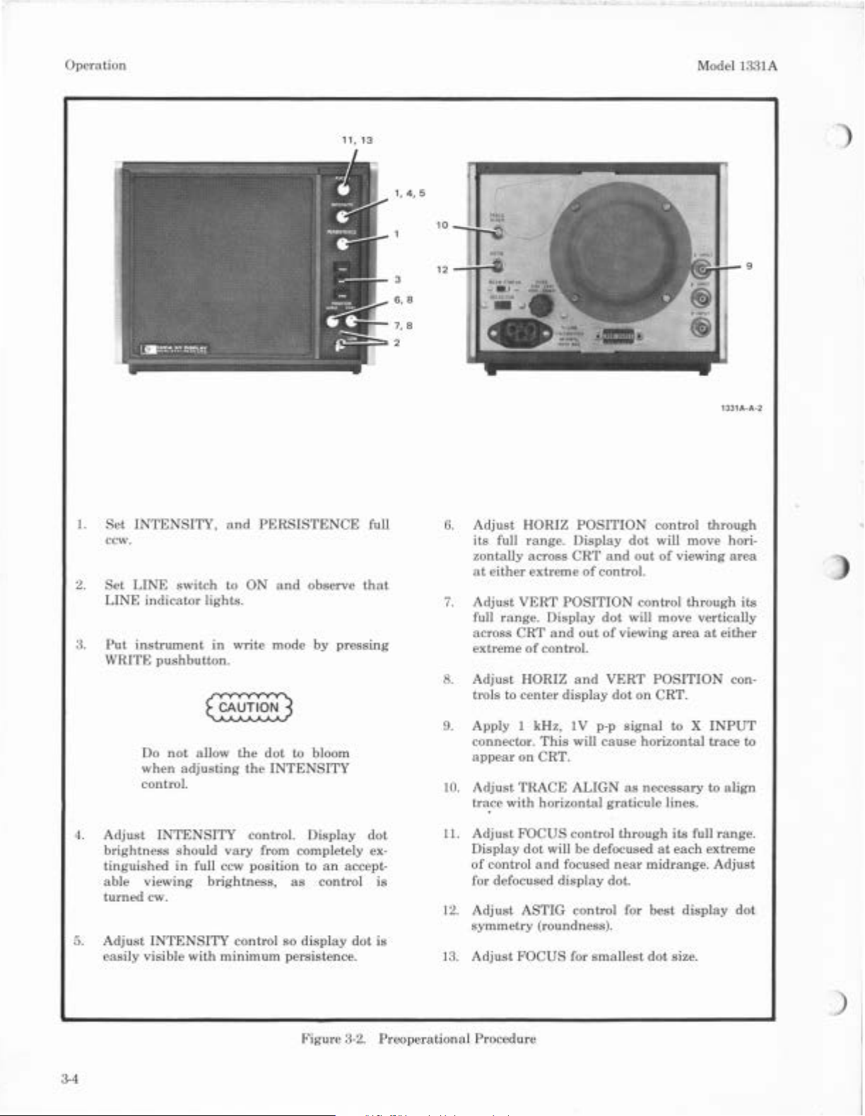
1.
Set
INTENSITY,
ccw.
2.
Set
LINE
LINE
indicator
3.
Put
instrument
WRITE
Do
when
control.
4.
Adjust
brightness should
tinguished
able
viewing
5.
turned
Adjust
eas
cw.
INTENSITY
ily visible
and
switch
to ON
lights.
in
write mode by press
pushbutton.
not
allow
adjusting
INTENSITY
vary
in
full ccw position to
brightness,
control
with
minimum
PERSISTENCE
and
the
dot
to bloom
the
INTENSITY
control.
from co
as
so
display
persistence.
observe
Display
mpl
etely ex-
an
accept-
control is
dot
full
that
ing
dot
is
6.
Adjust
its
zontally
at
either
7.
Adjust
full
across
extreme
Adjust
8.
trols
9.
Apply
connector.
appear
10.
Adjust
trace
11.
Adjust
Display
of
control and
for defocused
12.
Adjust
symmetry
13.
Adjust
HORIZ
full
range.
across
extreme
VERT
POSITION
range.
CRT
of
Display
and
control.
HORIZ
to
center
display
1 kHz, 1 V p-p
This
on
CRT.
TRACE
with
horizontal
FOCUS
dot
will
focused
display
ASTIG
(roundness).
FOCUS
POSITION
Display
CRT
and
of
control.
control through
dot
will
out
of
control
dot
will
move
out
of
viewing
and
VERT
will
cause
ALIGN
dot
signa
on
as
POSITION
CRT.
l to X
horizontal
necessary
graticule
control through
be
defocused
near
at
midrange.
dot.
contro
l for
best
for
smallest
dot
move
viewing
through
area
lines.
its
full
each
display
size.
horiarea
its
vertically
at
either
con-
INPUT
trace
to
to
align
range.
extreme
Adjust
dot
3-4
Figure
3-2.
Preoperational
Procedure
Page 23
(
Model 1331A
Operation
1.
Perform
3-2).
2.
Press
3.
Adjust
trols for desired
display.
4.
Press
5.
Press
6.
Press
preoperational
TO
WRITE
WRITE
INT
Excessive intensity
ence
duces
stored.
STORE
WRITE
ERASE
pushbutton.
ENS
ITY
and
brightness
NOTE
when
writing a display
the
time a display
TO
STORE
pushbutton.
TO
ERASE
pushbutton.
pushbutton.
procedures (figure
PERSI
and
and
STENCE
duration
persist
-
re-
can
be
con-
of
(
7.
Erasure
each
new
cases
where
are
to
3-4).
Figure
should
be
displayed
3-3.
take
piece
two
or
General
place
of
information,
more
pieces
simultaneously
Operating
prior
to
of
information
Procedure
writing
except
(Figure
in
1331A·A-3
3-5
Page 24
Operation
Model 1331A
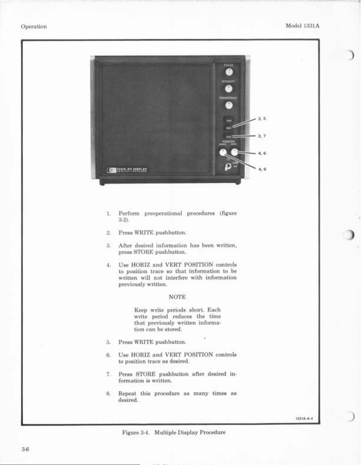
1. Perform
3-2).
2.
Press
WRITE
3.
After
desired
press
STORE
4.
Use HORIZ
to position
written
previously written.
Keep
write
that
tion
5.
Press
WRITE
6.
Use
HORIZ
to position
7.
Press
STORE
format
ion is written.
preoperational
pushbutton.
information
pushbutton.
and
VERT
trace
so
will
not
interfere
NOTE
write
periods short.
period reduces
previously
can
be
stored.
pushbutton.
and
VERT
trace
as
desired.
pushbutton
procedures (figure
has
been written,
POSITION
that
information
with
information
Each
the
time
written
informa-
POSITION
after
desired in-
controls
to be
controls
3-6
Repeat
8.
desired.
Figure 3-4. Multiple
this
procedure
as
many
Display
times
Procedure
as
1331A-A-4
)
Page 25
(
HEWLETT
II
PACKARD
CATHODE-RAY
The
cathode-ray
Oscilloscope
,warranted
failure
tubes and tubes
under this warranty.
claim shou
claims
nearest
We
neering evaluation helps us
you.
side
for
with
Hewlett
instrument
would
Please
of
this sheet and return
tube
(CRT) supplied in
and replacement
by
the Hewlett-Packard Company against electrical
a period
ld
Hewlett-Packa rd should be processed through your
manual).
like
fill
of
one year
with
phosphor
If
the
be
made
with
-Packard Sales/Service
to
evaluate every defective
out
the
CRT
Hewlett-Packard Company
1900
Garden
Colorado Springs, Colorado
Attention:
TUBE
CRT's
from
or
CRT
the responsible carrier.
to
provide a better
Failure
it
with
the
of
the
CRT
QA
WARRANTY
your Hew
purchased
the
date
mesh burns are
is
broken when received, a
Office
(listed at rear
CRT.
Report
defective
Gods Road
CRT
80907
lett
from
of
sale.
not
All
This engi-
product
on
the reverse
to:
-Packard
hp
are
Broken
included
warranty
of
for
5950-7124
To
avoid damage
the shipping instructions below; warranty
on broken tu
It
is preferable
replacement
is
not
available, pack the
below:
1. Carefully wrap the tube in 1/4 inch
batting
2. Wrap the above in heavy
3.
Pack wrapped tube in a rigid container which
at
dimension.
4. Surround the tube
excelsior
sure
to
the
tube
while
bes.
SHIPPING
that
CRT
carton.
or
other
lea
st 4 inches larger than
or similiar
the
packing
INSTRUCTIONS
the
defective
If
the carton
CRT
soft
padding material.
with
at
shock absorbing material;
is
tight
all around the tube.
in
shipment, please
CRT
according
kraft
paper.
least 4 in ches
Thank
CRT Dep:J
credit
is
not
be
returned in the
or
packaging material
to
the
instructions
thick
cotton
the
tu
be
in
of
packed
you,
rtment
allowed
is
each
be
follow
. ,
I
HEWLETT-PACKARD
COMPANY
1900
GARDEN
OF
THE
GOOS
ROAD, COLORADO
SPRINGS, COLORADO,
U.
S.
A.
Page 26
r
.........
"""-'-.__....~~
i
.......,;............-_
...
___
---.,.;;...
**
'srt'
1 !
.,
I
I (
"'I
'HU
FROM:
1.
HP
2.
HP
3. CRT
4.
Please
face below.
HEWLETT.
CATHODE-RAY
instr
ument
MODEL
instrument
SERIAL
describe the failure and, if.possibl.
SERIAL
NO.
NO.
NO.
____
TUBE
-----------------------
-----------------------
....;;._,
______
e,
PACKARD
FAILURE
....;;_
show the trouble on the appropriate
REPORT
_____________
_
CRT
I
HEWLETT
5. Warranty claimed ?
6.
HP
Sales
/Service Office
-PACK
ARD
COMPANY
1900
______
GARDEN
Yes
Of
___
THE
_ No
_
Repair
GOOS
ROAD, COLORADO
____
Order No.
_
------
SPRINGS,
COLORADO
)
, U. S. A .
t
Page 27
Model 1331A
Theory
c
PRINCIPLES
4-1.
INTRODUCTION.
4-2.
This
section
the
principles
It
also
contains
1331A keyed to
block
planation
is provided
diagrams
of
contains a simp
of
variab
le
persistence
functiona
an
of
circuit
circuit functions, keyed
after
the
block
l descriptions
overall block
groups. A detailed ex-
diagram
lified
diagram
to
the
discussion.
4-3. VARIABLE PERSISTENCE
AGE .
4-4.
The
following simplified
vided to give the
overall operation
4-5.
THE
4-6.
The
storage
ventional electrostatic deflection electron
aluminized
tional electron
write
gun.
second electron
shaping
beam
collector
and
the write
4-7. The
gun
e
mit
cloud (flood electrons)
toward
collector mesh.
on
The
metallic
4-8.
and
transparent
coating
action
ing.
dielectric
the storage
tion,
Because
face drops to
flood electrons
collector mesh.
mesh, and a storage
variable
gun
flood
's
horizontal
a cloud
the
the
inside
collector
mesh
The
action
variable
consisting
takes
This
surface
material
the
storage
of
reader a better
of
the
instrument.
STORAGE
phosphor
Additionally,
persistence elements
and
of
electrons from
storage
of
persistence possible.
metallic
place
mesh
the
about
CRT
CRT
viewing surface.
gun
in a storage
gun
(called
and
accelerator grids, collimator, a
the
viewing
gun
is
located
deflection plates.
mesh by
The
collimator
the
funne
mesh
located
is
just
of
the
storage
mesh
of
a dielectric
on
the
is
called
causes
and
the
mesh
capacitive
-10
are
repelled
explanations
understanding
.
(figure
the
is
an
capacitive
is
volts.
4-1)
storage
the
mesh.
phosphor.
just
its
cathode.
shaped
the
is
a conductive
l section
electrically
behind
mesh
covered
outside
the
storage
storage
held
coupling,
In
and
contains
tube
CRT
flood gun), flood
These
are
located between
outside
Its
and
collimator
of
the
the
storage
makes
It
is
an
with
material.
surface
coupling between
surface.
at
about
the
this
condition,
collected
SECTION IV
explanation
and
storage.
of
Model
and
schematics,
AND
STOR-
are
pro-
of
the
a con-
gun
and
an
The
conven-
is
called
contains
function is to
The
accel
CRT
transparent
electrically
of
surface. The
storage
the
storage
the
write
electron
erated
and
the
coating
glass.
mesh.
storage
a special
Storage
the
coat-
In
opera
+4
volts.
sur-
the
by
the
of
to
a
-
OF
OPERATION
4-9.
The
discussion
sumed
write gun is now
energy
strikes
trons
off
electrons
ever
surface, the
loss
more positive, flood
strike
the
(and
4-10. SECONDARY EMISSION RATIO .
4-11.
curve
ratio
storage
the
electrons
ber
over
more electrons
of
than
4-1
4-
of
erase
mesh
storage
areas
is
are
mesh
released
dropped
timing
RC
14
+
mesh
face
erase
returned
applied
Model 1331A.
that
th e write gun
is
much higher
the
storage
already
(secondary emission).
are
collected
the
write
gun
potential
of
electrons. Because
the
phosphor
pattern
stored)
storage
arriving
the
leaving,
2. ERASE CYCLE .
13.
the
pressed,
brought
, + 1
charging
volts.
to
10
volts. All
traced
on
Figure
of
is
point
storage
Figure
potentials
cycle.
is held
are
period
and
timing
4-2
the
storage
the
basis
surface
surface.
leaving
is
the
are
surface
the
4-3
Prior
at
surface
near
the
to
58
volts. When
both
storage
to
approximately-12
of
action
Capacitive
the
storage
follow
to
to
and
period,
+4 volts
these
the
storage
in
the
turned
on
the
and
called a crossover point.
secondary
to
+4
are
0 volt. When
storage
the
approximately
on, the electron
surface
the
storage
by
electron
at
gun
electrons
viewing screen.
by
the
storage
is
the
surface.
for
storage
for
erasure
The
the
storage
leaving
rises;
potential
graphica
on
the
initiation
volts.
at
-10
mesh
same
mesh
brings
coupling between
surface
rise to 0 volt.
the
and
actions
mesh
previous
was turned
than
with
The
the
collector
beam
that
point
these
write
surface.
secondary
The
of
point
where
surface
emission
than
arriving,
when
decreases.
lly
shows
storage
of
The unwritten
volts
the
and
potential as
the
ERASE
and
.5 volts.
the
causes
storage
the
are
caused
by
paragra
the
flood electrons)
suc
h force th
surface
secondary emission
strikes
rises
points
pass
In
gun
beam
emission
secondary
information
of
information
the
equals
ratio
more
the
surface during
the cycle,
and
ERASE pushbutton
the
storage surface
pushbutton
storage
During
800 milliseconds,
storage
the
At
the
mesh
storage
by
the pul
ph
off.
If
beam
(whose
at
elec-
are knock
mes
h. Wher-
the
storage
due to
have
become
through
this
manner,
is
written
ratio
emission
on
from
number
the
num-
At
a cross-
= 1.
When
the
potential
are
arriving
variations
the
storage
areas
of the
the
writte
the
collector
surface
an
erase
mesh
up
the
storage
storage
end
of
potential
surface
waveforms
se circuits
as-
th
ed
the
and
the
of
the
is
are
an
to
sur-
the
is
to
in
e
n
4-1
Page 28
Theory
Model 133
1A
4-14.
After
the
erase
cycle,
previously
formation
is
ready
(with
storage
where
pass
phor
post
4-15. VARIABLE PERSISTENCE.
4-16.
in
the
on
the
persistence would
Model 1331A does
it
uses a
varied.
method
all
information
there
the
has
to
store
much
higher
surface
they
strike
through
these
viewing
accelerator.
It
is possible
CRT
so
phosphor
method
Variable
of
removing
until
the
natural
storage
been
removed
new
information.
than
crossover
in
a positive direction
the
storage
areas
and
screen
that
by
to
disable
the
write
viewing
depend
not
use
that
permits
the
gun
surface.
only
persistence
stored
written
ERASE
on
the
pushbutton
time
(in excess
and
surface. Flood electrons
are
high
on
this
CRTs
information;
storage
elapses.
4-17.
Figure
persistence
shows
The
that
shaded
unwritten
In
the
write mode,
the
storage
increased
tively
While
at
of
the
storage
electrons.
written
storage
ward 0 volt.
mesh
returns
face
drops
surface
return
to a
initial
the
and
is
potential.
ability
capture
slightly
4-18. A train
written
4-4.
The
by
varying
effect, noticible
background
mesh
is pulsed positive, flood electrons
all
areas
screen,
4-19. STORAGE.
4-20.
to
the
even
In
storage
4-4
is
obtained.
the
area
and
written
mesh
this
increased
surface
This
areas
because
mesh
and
At
to
10 volts.
return
to
potential
of
the
flood
reduced.
of
trace
as shown
persistence
the
glow
of
the
ly
exciting
store
mode,
mesh,
graphically
storage
shows
areas
short
and
the
10 volts
for
The
mesh
the
erase
storage
the
shows
left
potential
of
potential,
attract
tends
to
the
the
end
its
normal
The
unwritten
-10
slightly
This
decrease
post
gun
electrons,
erase
by
of
repetition
under
and
lower
the
capacitance
storage
of
the
level
volts
and
more
accelerator to
pulses
the
some
gradually
the
shaded
written
rate
of
conditions,
on the CRT. While
mesh
to
the
entire
erase
and
persistence
the
pulses
written
the
storage
Write
gun
energy)
only
charge
in
pulled to
potential
the
storage elements
beam
writes directly
In
such
the
type
phosphor.
mode
of
operation;
the
persistence
require
otherwise,
surface
is
pressed
of
15
how
side
of
the
is
fixed
at
of
the
storage
pulses
duration
surface
the
ciwture
the
are
applied
is
of
the
written
flood
potential
between
surface
pulse,
and
areas
negative
in
charges
the
the
storage
of
the
written
potential
the
than
reach
and
trace
brightness
erases
areas
trace
the
pulses. A side
is a light
the
pass
phosphor
surface.
are
not
(store time)
in-
surface
electrons
the
the
areas
the
phos-
on
the
a mode,
to be
some
remains
or
until
minutes)
variable
graph
+4
volts.
both
the
surface.
to
capaci-
pulse.
areas
gun
of
the
the
to-
storage
sur-
storage
areas
their
reduces
through
the
in
figure
is
varied
storage
through
viewing
app
lied
is
iimited
This
ionization
electrons.
positive
phosphor
ground
positive
mode
for
4-21. STORAGE PRECAUTIONS.
4-22.
surface,
tential.
verted
pation
electric
trace blooming.
should
ing
primarily
occurs
The
and
illumination
is
by
brief
periods
When
they
The
to
heat
rating
material.
always
occurs.
by
an
effect called
on
the
of
residual
storage
storage
surface
gas
surface
molecules
gradually
allows flood electrons to
viewing
reduced (
keeping
area
until
and
the
to
refresh
write
gun
cause a very
energy
and,
of
the
from
when
storage
The
The
intensity
be
set
below
where
the
display
store
time
flood
gun
the
electrons
this
it
exceeds
burning
the
display.
rapid
sudden
surface,
and
by
penetrate
they
increase
is obscured.
increased) in
turned
strike
increase
change
the
action
level
of
point
fade
positive.
is
caused
flood
charges
off
the
heat
burns
is
visible
the
write
where
by
gun
more
to
the
back-
Fade
stor
except
storage
in
po-
is
con-
dissi-
the
di-
as
gun
bloom-
e
4-23. BLOCK DIAGRAM DISCUSSION.
4-24.
This
discussion
the
circuit
on
the
4-25. LOW VOLTAGE POWER SUPPLIES.
4-26.
blocks,
puts
+12.5V,
and
to it.
4-27.
4-28.
high
volts for:
volts for
post
ment,
high
trols
by
controlling
4-29. X- AND Y-AXIS AMPLIFIERS.
4-30.
and
groups
overall
This
block
block provides power to
including
at
four
de
and
+158V.
all
the
other
The
+ 12.6V
HIGH
VOLTAGE POWER SUPPLY.
The
high
voltage
the
the
potentials
write
write
accelerator.
hv
adj,
and
voltage
the
power
intensity
The x-and
serve to drive
deflection plates.
trols
are
included
and
phase
shift
illust
(blocks) to
diagram,
the
high
voltages
low
supply
voltage
The
voltage
is
are
-50V
power
to
gun
cathode,
gun
grid, and
The
write
the
FOCUS
supply.
and
blanking
the
voltage
y-axis
amplifiers
the
CRT
POSITION
in
these
adjustment.
rates
the
each
other.
figure 4-6.
voltage
power
supplied: +50V,
supply
supplies
also
adjustable.
supply
operate
the
approximately
+7.5 kilovolts
gun
intensity
control
The
gate
functions
to
the
write
are
horizontal
and
BEAM
blocks
as
well
relationships
It
is
based
all
the
oth
supply.
Out
-50V,
is
adjustable
are
referenced
provides the
CRT:
-2915
-29
for
limit
adjust-
are
part
of
amplifier con-
of
the
CRT
gun
grid.
nearly
identical
and
vertical
FIND
con-
as
the
gain
of
er
55
the
the
-
)
4-2
Page 29
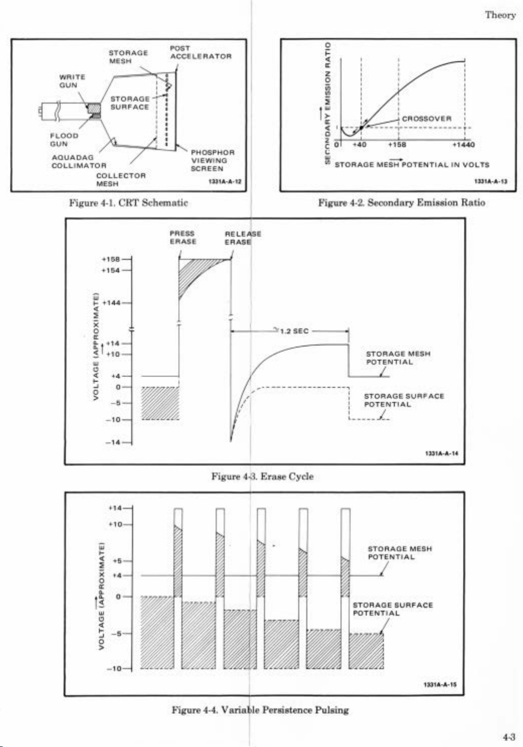
Th
eory
WRITE
GUN
FLOOD
GUN
AQUA
DAG
COLLIMATOR
Figur
STORAGE
MESH
STORAGE--:--:
SURFACE
COLLECTOR
MESH
e 4-1.
CRT
+158
+
154
iii
t-
+
144
~
::?
x
0
a:
~I
+14
:!
+
10
w
(!)
~
+4
t-
_J
0
0
>
- 5
-
10
-
14
POST
ACCELERATOR
:i
I
1 :
I O
I O
I O
I 0
I a
•
•
Schematic
PRESS
ERASE
J
I
-
PHOSPHOR
VIEWING
SCREEN
1331A-A-12
RELE
SE
ERAS
i----1---
/ :
"'~
1.2
SEC
----<ot•
....
--
-----
----
'I/ :
,'
0
i=
~
a:
z
0
(/)
(/)
::?
t~
a:
~
0
~ -o+--+4~0
(.;
w -
"'
Figure
I
I
I
I
I
I
I
I
I
I
I
I I
1
~/
lr
~
I
---
--
h I I I
---
STORAGE
4-2.
Secondary
1
STORAGE
POTE
----
--
,
STORAGE
POTENTIAL
~-----.L-
~CROSSOVER
J
-- ---~---
+-1~5-8
_____
MESH
POTENTIAL
MESH
NTIAL
SURFACE
----
-----t -
+_1_4._4
IN
Emission
1331A-A-14
1
I
0
VOL
1331A-A-13
Ratio
TS
+
14
+
10
w
t-
~
+5
::?
x
+4
0
a:
a..
0
t~
w
(!)
~
~
- 5
0
>
-
10
Figure
Figure
4-4. V
aria
4 .
Erase
le
Persistence
Cycle
Pulsing
STORAGE
POTENTIAL
STORAGE
P
OTENTIAL
MESH
SURFACE
1331A-A-15
4-3
Page 30
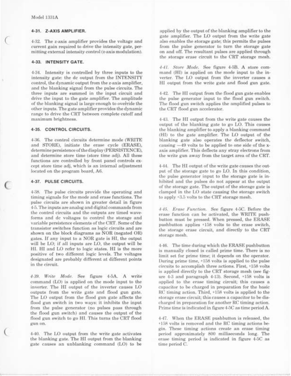
(
(
Model 1331A
4-31.
Z-AXIS
4-32.
The
current
mitting
4-33.
4-34.
INTENSITY
Intensity
intensity
control,
and the bl
three inputs
drive
the
of
the
blanking
other
inputs. The
ra
ng
e to drive the CRT between co
maximum
4-3
5.
CONTROL
4-36. The
and
STORE),
determine
and
determine
functions
cept
store
loc
ated on
4-3
7.
PU L
4-38.
The
timing
signals
pulse circuits
4-5. The
the
control
forms a
variable
transistor
shown
gates.
will
HI.
on
If
be
LO;
HI and
positive
designated
in
the
circuit.
AMPLIFIER.
z-axis
gain
external
gate:
the
anking
input
amplifier
required to
intensity
GATE.
is
controlled
the
de
dynamic
signa
are
summed
to
the
output
signal
gate
amplifier
brightn
control
ess.
CIRCUITS
circuits
initiate
persist
ence
of
store
time
are
controlled
time
adj,
which
the
program
SE
CIRCUITS
pulse circ
inputs
circuits
nd
de voltag
persist
switches
the
any
if
block
input
uits
for
the
mode
are
shown
are analog
and
es
ence
elements
function
diagrams
to a NOR
all
inputs
LO refer to logic
of
two different logic l
are
probably
provides
drive
the
control
by
output
from
from
l from
the
in the
gate
amplifier.
is
large enough
.
determine
the
erase
the
display
(store
by
front
is
an
board, A6.
.
provide
and
in
greater
and
digital
the
outputs are
to control
of
as
as
gate
are
LO,
states.
different
the
voltage
intensity
gate,
(z-axis modulation
three
inputs
the
INTENSITY
the
z-axis amplifier,
pul
se
circuits.
input
circuit
The
amplitude
to override
provides the
mplete
mode
dynami
cutoff
(WRITE
cycle (ERASE),
(PERSISTENCE),
time
adj). All these
panel
controls ex-
internal
the
erase
adjustment
operating and
fun
ctions.
detail
in
commands
tim
ed wave-
the
storage
the
CRT.
Some
logic c
ircuits and
NOR
(negated
is HI, the
the
HI
eve
ls.
at
different
output
The
output
will be
is the
voltages
and
per-
to
the
The
and
the
and
The
figure
from
and
of
the
are
OR)
more
points
4-39. Write Mode. See figure 4-5A. A write
mmand
co
invert
outputs
The
flood
from
the
flood
gun
4-40.
the blan
gate causes
(LO) is
er.
The
from
LO
output
gun
switch
the
pulse generator
flood
gun
gun
switch
on.
The
LO
king
app
HI output
the
write
from
in
switch) a
to
go
output
gate.
The
an
unblanking
lied
the
two
nd caus
HI.
from
HI
on
the
of the
invert
gate and
flood
gun
ways:
it
(no
pulses
es
This
turns
the
write
output
command
mode
input
er
flood
gate
inhibits
pass
the
output
the
gate
from the
(LO) to be
to
causes
gun
gate.
affects
the
input
through
of
CRT
flood
activates
blanking
the
LO
the
the
app
lied by
gate
also enabl
from
on
the
and
storage
).
4-41.
ma
nd
verter.
HI
output
-42. The
4
the pulse
The
c
th
e C
4-43.
outp
ut
the
blanking
(HI) to
blanking
causing
ax
is amplifier.
the
write
4-44.
put
of
the
pulse
hibited
of
the
c
lamped
to
apply
4-46. Erase Function. See figure 4-5C. Before
e
rase
button
pushbutton
the stor
storage
4-46.
is
manually
limit
During
circ
uits
is applied directly to
ure 4-3 a
app
lied to
ca
pacitor to
RC
timing
storage
c
harged
Prime
47.
4-
+ 158 volts is removed a
gin.
period a
erase
the
amplifier.
es
the
the
pul
se
output
of
The
LO
storage
generator
the
gate;
off. The resultant
erase
circuit to
Store Mode.
(HI) is
The
LO
from
HI
generator
flood
gun switch
RT
flood
The
HI output
of
the
amp
the
gate
gate
-49
volts to be
gun
The HI output
the
storage
generator
and
the
storage
in
the
+3.5
vol
function
must
be
applies
age
erase
See
app
lied on
output
the
output
from
write
from
input
appli
gun
accel
erator.
from the
blanking
gate
lifi
er
to apply a blanking command
amplifier.
also
operates
applied
This
deflects a
away
from
of
the
gate
to go LO.
input
pulses
gate.
LO
ts
can
do
The
outp
state caus
to
the
CRT
be
activate
pressed. When pressed,
+ 158 volts to
circuit, a
mes h.
Th
e time
set
during
closed
for
prime time; it
is
which
called
prime time, + 158 volts is
to accom
nd
erase
in
time is
When the
plish
paragraph
the
erase
be
charged
action.
Third
circuit;
this causes a capacitor
preparation
indicated
ERASE
thr
the
CRT
4-13). Second, +158
timing
in
, +158 volts
for
in
figure 4-5C
nd
These
ppr
timing
timing
oxim
ate
period is
actions create
ly 800 milliseconds long. The
indi
blanking
output
from
this permits
to
turn
pulses
are
the
CRT
figure 4-
the
gate
the
to
es
5B. A
mode i
the
inverter
and
flood
the
flood
the
amplified pulses to
write
to go LO.
The
LO
the
to
ny
stray
the
target
write
gate cau
In
to
the
storage
not
appear
ut
of
the
ing
the
stora
ge
d, the WRITE
the
nd
directly to
the
ERASE
prime
depends
applied
ee
act
ions.
storage
circuit;
preparation
another RC
pushbutton
the
RC
timing actions be-
cated
in
amp
the
the
storage
applied
storage
nput
lifier to
write
the
store
pulses
through
mesh.
to
the
the
gate
gate
com-
in-
causes
flood
gun
gate
gun
gate
enables
gun
switch.
gate causes
This
output
the
causes
of the
deflector switch,
one
side
of
the
elec
trons
from
area
of
the
CRT.
ses
the
out-
this condition
gate
is in-
at
the output
storage
storage
gate
switch
mesh.
the
push-
the
ERASE
erase
switch,
the
CRT
pushbutton
time. There
on the
First,
mesh
this
for
is
applied
is
operator
to
the
pulse
+ 158 volts
(see fig-
volts
causes
the
basi
to the
no
is
to be dis-
timing
as
time
action.
period A.
is released, the
an
erase
timing
figure 4-5C
as
a
.
x-
,
is
.
a
c
time period C.
Page 31

Theory
l\1odel 1331A
4-48.
Some
of
the
waveforms
4-5C
are
A).
present
Others
are
only
present
during
only
period (time period C). Still
both
prime
plus
the
4-5
as
4-49.
output
differe
levels.
C.
One
ac
tivates
activates
4-50. Because
any
time
generator
prevent
gun
switch
output
time
erase
timing
time period
The
erase
lines.
Two
nt
circuits
Both
output
output
the
blanking
the
collimator
line
the
Model 1331A is
must
be
pulses
from
from
to
the
the erase
and
B.
switch
output
require
lines
disables
flood
disabled
being
flood
the
period
gate.
driver.
gun
not
switch
generator.
4-51.
One
input
to
the
blanking
activated
erase
period
to be LO
4-52.
the
gate
tend
RC
current
the
of a charging
the circuit
path
stabilizes
C,
the
circ
coupled to
4-53.
time period B.
apply
It
also
volts to
assure
reach
switch
C.
The
write
are
to
curve
from
output
is
pulse
uit
is
The
the
one
that
the
during
activates
This
causes
during
HI
from
gate
LO; now
LO
so
the
go
HI.
Its
because the
the
storage
of
the
capacitor.
takes
less
cut
off
and
in
its
HI
generator
turned
the
off,
CRT
output
This
blanking
causes
the
side
of
no
electrons from
target
pulse
period A.
another
the
both
the
inverter
both
output
rise to
storage
storage
current
the
output
state.
is
and
storage
of
the
blanking
causes
signal
deflector
the
x-axis amplifier.
area
of
cycle.
4-5
4.
DETAILED
4-5
5.
The
a guide to
ment
and
For
instance,
tions
as a Darlington
following
understanding
are
not a discussion
the
CIRCUIT
paragraphs
text
may
amplifier
the
indicat
prime
during
others
erase
is
initiates 3 actions
lines
are
different
go
HI
the
pulse
The
switch
in
store
during
applied
gun
accelerator.
output
of
ed
time
the
erase
are
present
cycle.
indicated
required
operating
during
generator
other
is
activated
mode,
time
through
disables
gate
was
The
HI
input
during
the
blanking
on
figure
(time period
timing
during
Prime
in
time
figure
on
because
voltage
time
period
and
output
line
(Al)
the
pulse
period C to
the
flood
The
HI
the
pulse
previously
from
the
pulse
gate
periods (pulse period B).
holds
the
output
inputs
of
the
the
erase
gate.
The
erase
As
the
until
At
the
enabled, the
the
erase
to
storage
HI
state
circuit
rising
circuit is
capacitor
, finally,
of
the
end
of
storage
pulses
the
storage
gate
will be
is
robbing
voltage
the
charges,
its
charge
storage
time
are
will
an
result
gate
period
erase
again
mesh.
gate
is
LO
during
the
(HI) to
switch
the
CRT
blanking
the
the
gate
write
during
amplifier
amplifier.
to
apply
These
the
actions
gun
erase
-49
will
THEORY.
are
functioning
of
basic
state
that
and
assume
intended
of
the
electronics.
a circuit func-
instru-
that
as
the
of
at
to
reader
usual
The
matics
the
eac
be folded
2
4-56. LOW VOLTAGE POWER SUPPLIES.
4-57.
voltages to four
-50volts,+12.6
power
a
each of
4-58.
1331A
vac (single
Sl
former
primaries
for
current
4-59. Secondary
voltage
rectified
rectifier is filtered
former
DSl
4-60.
sample
Any
with a reference
the base
applied to
is
the
4-61.
+50
the
sample
pared
amplified
Series
direction
4-62. + 158 Volt Regulator. See
+ 158 volt power
volt power
in
reference voltage.
and
is driven
the
knows
circuits
detailed
located
appro
priate
h discussion.
out
The
low voltage power
supplies
secondary
the
de
Primary
can
be
phase,
applies
230
power to the
Tl.
SELECTOR
in
parallel
vac
operation.
from
across
by a bridg
Tl
also
and
6.3
vac
-50
Volt Regulator. See
of
the
error
is
of
AlQ4.
the
driven
by
error.
+50
Volt Regulator. See
volt
power
-50
volt
of
the
to
the
by
regulator
as
to
supply
the
+ 158
volt
applied
to
by
error.
how a
Darlington
will
be
explained
circuit
in
theory
Section
schematic
The
indicated
VIII.
at
for reference
regulated
volts,
and+
158 volts.
consist
power
outputs
Powe
operated
of a primary
circuit,
.
r.
See
from
and a regulator
48 to 440 hertz).
primary
switch
for 115
damaging
Pow
each
secondary
Line
the
er.
vac
fuse
instrument.
See
e rectifier.
and
applied
supplies
for
output
felt
at
base of
A1Q3
supply
power
output
voltage
12
the
CRT
is
selected
the
base
(developed
The
difference
A1Q3.
in
such
is
referenced to a
supply
of
the
a direction
reference voltage.
AlQ2
and
applied
QI
is
driven
correct
the
A5Ql
the
error.
supply
power
The
base
is
at
the
base
supply
difference is amplified by A5Q2
of
A5Ql.
in
such
a direction
amplifier
in
greater
is
keyed to
A reference
the
pertinent
schematic
while
reading
supplies
de
voltages;
The
power circuit,
schematic
either
115 vac,
LINE
windings
S2
connects
operation
Fl
prevents
schematic
winding
The
output
to a regulator.
vac
for
LINE
filament
.
schematic
at
the
rotor
of
A1Q5
and
by
is
amplified
Series
regulator
as
schematic
at
the
base
+50
volt
supply
The
difference
to
the
base
by
AlQl
schematic
referenced to
of
A5Q2.
is
compared
Series
regulator
as
works. Un-
detail.
the
sche-
is
made
point
may
then
the
text.
convert
+50
line
volts,
low voltage
circuit
1. Model
or
230
ON
switch
of
trans-
the
two
or
in series
excessive
1.
The
is
full-wave
of
each
Trans-
indicator
1. A
of
AlR22.
compared
Al
VR4)
and
Q2
to correct
1.
The
sample
of
A1Q2. A
is com-
of
AlQl.
in
such
2.
The
the
-50
Any
error
to
the
Q3
to
correct
to
in
for
ac
on
of
is
a
4-4
Page 32

@ill
0-~SIA
+1
58 V _
__..:J
~""T"-<"-~
lsTORE
1/
-
I
~
0-
I
--j MO
!PERSIS TENCE! 6
+12.6
0
~
o-q
-+1581/
-~
L
J.9.S
li
!PERSISTENCE! 6 :
isTOREI
0-
--j MO
0
S2
A
10
I
O
S
3A
I
I
I
I
DE
S2B
1
(1
I
...
S2 A
3A
:o
I
DE
S2B
:o
INPUT
LO
ov
INPUT
HI
0.111
WRITE MOOE
A
LO
ov
STOR
MODE
-+101/
fl
ov
1-----t-1__'.
HI
+201/
LO
ov
J.J
J.Jlr-----tl-1__'.A::5:_::0::4_:2::_-•::•:...r-----•
HI
+0.71/
LO
ov
STORAGE
ERASE
A::5:_::0::4_:2::_-4::4
:...J
____
COLLIMATOR
DRIVER
A5Q50,
51
LO
X>-0;,.v~
.....
STORAGE
ERASE
COLLIMATOR
DRIVER
A5Q50, 51
HI
::X:>-+_i•_v_
...
.,
~
.,
Theory
TO
STORAGE
MESH
TO
COLLECTOR MESH
TO
COLLIMATOR
TOY
AMPLIFIER
!~~~TF~
ER
TO
STORAGE
MESH
TO COLLEC
TOR
MESH
TO
COLLIMATOR
TOY
AMPLIFIER
!~;~T~
ER
+158
!PERSISTENCE
l sTORE I
+12.61/
-~
1/
-
H
I I
! 6 :
0-
S2A
o
S3A
I
--j
MOOE
INPUT
52
8
I
0
A. PRIME TIME (TIME DURING
PUSHBUTTON
e. PRIME TI
Ce
800
MSEC
PRIME TIME
IS
ME+
STARTING
ACTIVATED
800
MSEC
AT
END
Figure
WHICH
OF
ERASE
4-5.
n ··
+5.8V
J
Lov
--.jA!-
Pulse
Ci ·cuits Block
ERASE FUNCTION
c
Diagram
1-B-.j
Ll
+20V
ov
_.,A
i.C~
.n.--
:- -
+1581/
J
Trim
+IMV
111
~-~+3.51/
----·-12.51/
TO
STO
RAGE
MESH
ro
y
AMPLIFIER
1331A1c-c-s
1331A/C-C-5
4-5
Page 33

(
(
Model 1331A
4-(i:J.
+ 12.6
Regulator.
ple
of
the
output
selected
power
ference) is amplified
of
such
4-64.
4-65.
turned
winding
Q5 occurs
the
distributed
cuit.
sequently
the
4-66. A sample
by A3R8)
A
sample
power
compared
(error) is amplified by A3Q3
difference drives
tertiary
correct
4-67.
rectified by A4CR1
C
components
ting
CRT
4-68.
to
variations
the
the
4-69.
from
amplifier
switch
are
amplifier to control
CRT. A3Q9
plifier. A3Q7
A3Q10 respectively.
4-70.
A 7
accelerator.
4-71. X- AND Y-AXIS AMPLIFIERS.
4-72. See
amplifiers
plifier will
and
compared
supply
A5Q3. Series
a direction
HIGH
See
on, Q5
circuit oscillates
The
voltage
supply
winding
the
The
potentials
write
The
the
return
total
brightness
There
the
(A5Q48/ A5Q49
summed
A portion
and
at
as
VOLTAGE POWER SUPPLY.
schematic
starts
of
A4Tl.
through
inductance
conduction
the
voltage
at
the
of
establishes
of
the
-2915
is
fed
with
the
error.
oscillations
on
to
gun.
output
side
in
the
voltage
of
are
INTENSITY
(schematic
and
and
and
provides
schematic
are
nearly
be
explained.
the
regulator
collector
the
the
of
A4
the
of
output
on
the
three
the
A3Q10 form a
of
See
schematic
of
the
12.6
volt
to a
sample
base
of
A5Q4.
by
A5Q4
and
Q4
is
to correct
3.
to
Positive
the
at a rate
angle
of
+50
a reference
back
reference voltage.
A4Tl
and
and
control
the
of
the
the
CRT.
potentiometer, from
composite
the
brightness
A3Q8
the
the
4.
identical,
the
When
the
conduct
tertiary
and
the
volt
base
are
A4CR2, filtered
gate
of
inputs
5),
on
are
cathode
potential
Because
through
feedback to
winding
capacitance
of
Q5 (class C)
output,
of
A3Q2.
volt
power
at
output
to
the
and
A3Q2.
of
A3Q5
in
such
stepped
A3,
and
grid
amplifier
control
the
gate
control
to
the
and
from
schematic 7).
signal
complementary
drivers
supply
only
2. A
power
applied
driven
error.
instrument
determined·
the
of
the
ba..;e
a direction
applied
and
grid
amplifier,
grid
(or
blanking)
for
the x-and
supply
of
the
-50
Any
error
to
by A5Q3
the
the
of
A4Tl
of
is
controlled
supply
base
of
high
of
A3Q3
Any
difference
The
amplified
through
up
by
by
the
as
cathode
is
connected
supply.
and
gate
amplifier:
the
the
intensity
The
drives
for A3Q9
is
tripled by
the
CRT
the
y-axis am-
sam-
is
volt
(dif-
the
base
in
is
first
primary
base
of
and
by
the
the
cir-
and
con-
by
(selected
A3Q3.
voltage
and
the
as
to
A4Tl,
Rand
opera-
of
the
Any
varies
controls
z-axis
inputs
the
gate
of
the
am-
and
post
y-axis
4-73.
The
input
stage
pairs (A5Q5A/ A5Q7
as
a differential
tion provides
the Y INPUT
amplifiers.
4-74.
Common
vides
variable
adjusting
The
4-75.
pairs
(A5Q55A/
a differential
A5
Ql
3.
differential
of
the
CRT. Vertical position
by
changing
halves
TION
shift
and
phase
amplifier is
is
of
beam
4-76. Z AXIS AMPLIFIER.
4-77. See
the input
te
control
plifier composed
A5VR8
volts;
4-78.
4-79. See
of
WRITE
time
4-80.
button
switch is
ERASE
and
applies
4-81.
button
that
WRITE
ting
The
PERSISTENCE
schematic
nects
generator.
of
control
(unequal
y-axis
shift
activated.
the x-and
cannot
nsity
gate
this
CONTROL
the
ERASE
adj
The
switch.
storage
The
switches
both
current
STORE switch,
the
the
and
gain.
vert
gain
output
pair
This
configuration
drive
the
the
differential
R7 is
amplifiers
adj
interrupted
This
y-axis
be
schematic
signal
which,
grid. The
limits
the
limits
schematic
switch
switch
+158
switch, when
circuits
ERASE
It
not
activated.
erase
volts to
WRITE
cannot
to
7.
When
store
on
and
emitter
required
the
current
emitter
Amplifier
potentiometer
stage
Ql4
and
with a common
for
the
division
adjusted. Compensation
output
deflected
switch,
applies
the
time
capacitance)
is
A5Cl3.
when
reduces
amplifiers
5.
The
to a level
in
turn,
z-axis
amplifier
of
A5Q53
collector
the
power
CIRCU
6.
the
switch
on
program
switch
will function
In
+158 volts to
circuits
the
and
that
are
be
activated
activated,
inverter,
when
control to
activated,
adj
consists
follower
amplifier
consists
A5Q55B/
of
amplifier
accomplished
The
the
off
capable
ITS.
The
assembly
WRITE mode,
storage
STORE
mechanically
control, A6R2, to
of
two
A5Q5B/ A5Q8)
pair.
This
high
input
impedance
drive for
A5Q9/ A5Q10 pro-
gain
is
A5R38.
of
two cascoded
Ql5)
current
provides
vertical
current
z-axis
drives
and
voltage
STORE
is a spring-return
on
A5Q35,
deactivated,
the
deflection
control
current
BEAM
the
control circuits
board
the
is
through
when
between
source for
FIND
gain
and
to
the
point
CRT
screen.
amplifier
of
driving
the
CRT
is a
differential
A5Q54. Zener diode
of
A5Q53 to 8.25
dissipated
switch, and
A8
A6.
only
when
the
schematic
mesh
switches
at
the
same
interrupts
on
pulse
STORE
Darlington
connected
configura-
for
the
following
controlled by
connected
the
accomplished
VERT
for
by
adjusting
switch
output
where
increases
write
by
and
the
pressing
erase
7.
of
the
are
connected
time.
the
schematic
connects
generator
switch
the
as
source,
required
plates
the
two
POSI-
phase
the
the
S3
range
the
the in-
gun
am-
A5Q53.
consist
the
the
store
push-
STORE
the
timing
It
also
CRT.
push-
so
The
opera-
the
on
con-
pulse
x-
7.
Page 34

Theory
4-82. PULSE
4-83. See
wavefo
sists
A5Q32,
The
control
set
set
This
generator
paragraph.
4-85.
junction
discharg
across A5R104. The spike
multivibrator. The
erates a negative going
wide
charges to 0 volt, A5Q32
c
rms
The pulse
persistence elem
4-
84.
Pulse Generator.
of
current
the PERSISTENCE control
on
full counterclockwise, will reverse
and
disable the
more
charges
When
at
harging
4-86. invert
amplifier that
a
transistor
(A5Q36) a
4-
87.
Flood
flood
gun
are common
inv
erte
rs
of the
ca
each other.
circuits
two inputs.
of
jun
4-88.
circuit c
A5C35.
the
base
volts
6, A5CR38
jun
+4.5
A5C55 to
because A5C52
prime
l
at
use
some
A5Q35
ction
Erase
anode
of
is
ction
volts.
ease
d), A5CR38
the
pulse
A5Q48
applied
time (when
junction
CIRCUITS.
schematic
on
figure 4-5 a
circuits co
current
and
monostable
through
schematic
clockwise, A5Q31 co
A5C24
frequency
A5C24
transistor
es A5C24, a
the
collector
again
er.
switch
nd
the
Gun
gat
e (A5Q36)
emitter
and tra
circuits. Two
of
Both
because both
Both
and
of
A5R113 a
Timing
onsists
The
input
of
A5CR38
and
of the two diodes
This
the
7. Also refer to
ntrol
ents
in
the
source A5Q31,
multi
A5Q31
6.
Either
pulse generator.
faster
as
charges
A5Q32,
nd
monostable
pulse
of
to
repeat
The
inverter
functions
to
control the flood
write gate
Gate
and
amplifiers
nsistor
the
both have a common
circuits
gates
can
have co
nd
switches
function
mmon
A5R114.
Circuit.
of
A5CR38, A5CR39, A5R123,
to
the
and
and
to
the
from
the
ERASE
A5CR39
positive
base of
is
of the
already
the
and
A5CR39
A5C52
ERASE
two
nd
figures 8-21, -22,
the
CRT.
The
vibrator
is
or
and
explained
to
the
generates
triggers
A5Q33.
turns
the
cycle.
as
a logi c
(A5Q37).
and
switches
need
be
activated
erase
its
base
turn on.
rises
change
turned
diodes
the
storage and
pulse
generator
relaxation
A5Q33/ A5Q34.
determin
by
the
store
of
these controls,
As
either
nducts
the
about
off
is
more
increases
in
the
firing
transistor
a positive
the
multivibrator
10 microseconds
When
and
a co
mmon emitter
inverter
Write Gate .
the
write
gate
that
function
to control the
are
to
be
isolated
as
negated
from
inputs
two
of
turn
at
The
erase
timing
outputs
A5Q52.
switch
The
voltage
from 0
is
coupled
but
it
has
on.
At
pushbutton
off. The voltage
drops
voltages
and
variable
oscillator
ed by
either
time
when
bias
A5Q31
control
current.
the
pulse
following
point
of
conducts,
spike
monostable
A5C24 dis-
A5C24
input
on
volt
starts
and
gun
gate
(A5Q37)
as
logic
outputs
required be-
from
OR
(NOR)
either
the
collector
at
timing
circuit is
are
to the
When
+ 158
schematic
at
to
about
through
no
effect
the
end
is re-
to 0 volt
and
-23.
con-
adj
uni-
gen-
as
The
of
the
and
at
the
of
is
Model 1331A
This
negative
ping
the
volts.
Immedi
through
to c
harg
A5Q52
This
is
4-89.
Erase
A5Q39,
transistor
mits
a la
input current.
on
and
volt. When the
time
pulse is
transistors
+l.4 volts.
collector
is
one
the
other
A5CR40
+0
.6
volts.
off
and
4-
90.
Blankin
is a co
mmon
invert
er
tr
olled from
functio
The
circ
the
o
During
and
from
During the
switch
th
period; consequently,
entire erase
4·
a
switch
eit
OR (NOR
pulse
the
mode,
pulses from
off
mode,
output
(800 milliseconds),
tends
because
circuit.
1·92. Stora
.
c
ns
three
uit
erase
utput
of
its
the
e er
ase
91.
Storag
common
and
her
of
generator
write gate
the input
so
that
the
is
to
ircuit
consists
change
voltage
ately,
A5R123 towa
e A5C35 to +1.4 volts (turn
and
A5Q39) is approximately
the bas
ic
Switch.
is
a Da
switch.
rger
current
Norm
the
collector
coupled to
turn
During
of
A5Q39 to
output
its anode rise
side
is
turned
When
of
of
g Gate.
emitter
and
transistor
any
as a three-input
inputs are:
from
the
switch
the
write
write mode, all
output
write
erase
is
HI
during
timing circuit
function.
e Gate.
emitter
logic
two
inputs,
) logic
the
the
output
clamped LO.
go
HI,
current
ge
is coupled
at
the
base
the
rds
timing
negative
off
A5CR40. When A5Q39
A5Q39
cat
is
gate
amplifier
inverter.
gate.
at
at
from
pulse
outp
from
is being
Erase
of
for
The
rlington
The
Darlington
to
ally,
of
going
until
this
+50
volts.
the
erase
on and
is
s to +4.7 volts.
The bla
amplifier
switch.
of
three
the
hode
at the ano
gate
from
three
HI.
During
is
function,
prime time
is
the
The storage
it
also
The
the
collector
the
collector
the
generator
ut
is a train
the
During
both
inputs
but the
drawn
Circuit.
switch
A5Q42
through
of
A5Q52
capacitor
+50
volts.
the
erase
erase
pair
be
switched
both
transistors
A5Q39
transition
the
base
A5C35
time,
A5CR
The
switch. The
its
anode
turned
nking
that
Because
different
negated
output
of
A5CR39,
de
of
the
of
store mode, the
HI
and
the
input
HI
during
output
functioning
Because
fundions
two
inputs
of
of
write
gate
turn
write
the
are
change
by
The
and
A5C35, droptoward
starts charging
The
time
required
on voltage. for
800
millis
cycle.
switch,
functioning
is
charges
off, A5CR40
func
of
collector
its
its
and
is
it
of
gate
erase
LO
A5Q52
configuration
with a small
are
clamped nea
of
the
of
A5Q52,
back
51
clamps
collector
OR
the erase timing
A5CR40,
the
gate,
is
A5Q33,
A5Q37.
the
pulses. In
is
the
Darlington
of
other
is
turned
is
clamped
gate,
tions
as
it
can
inputs,
(NOR) gate.
the
output
and the
of
inputs
output
from
the
the
input
erase
LO
during
A5Q41 ,
as a transistor
activated
as a negated
are: from
and
In
is
LO
and
gate
is
HI
and
timing
and
the
an
RC
storage
storage
-4.5
eco
nds.
and
as
per-
turned
r 0
prime
both
up to
the
A5Q39
is
at
on,
to
turns
A5Q48,
a logic
be
con-
it
also
of
A4Q37.
are
LO
input
is
LO.
erase
from
timing
the
is
from
the
from
write
the
on
and
store
the
period
output
curve
erase
erase
pair
a
4-6
Page 35

r-
I x INPUT I
L -
-.,"'
_l
JI
Theory
I
HORIZ
0
I
I
I
I
I
•
I
I'""'.
I
I
I
I
I
I
0 I
I
I
I
POSITION I
HORIZ GAIN
• PHASE
I
I
I
VERf-----pQ$1TION
SH I FT
VERT GAIN
ADJ
rBEAMFiNO"
0
.__
-
_
-""
I
_.
,...-,
1
0N
...
I
0
n
t
-
50V
ly~N;;;;Tl
l..-
_'.....! :
J2
r
---,
Lz
~NP~T
J3
I PERSISTENCE I
I WRITE I
I
STORE
ERASE I
I
:
I
r-~,
l
_J
:
I
,---1
I CONTROL
0 -
--
-l
0-
----1=:_
I
0--------
o-----r--
I
I
STORE
TIME
ADJ
·---1-
I
I
-
L
CIRCUITS
FRONT PANEL
PROGRAM
BOARD
___
DEFLECTION
J
~
FLOOD
GRID ADJ
'f
CIRCUITS
COLLIMATOR
ADJ
I
GUN
PULSE
+50V
r
WRITE
DEPTH
ADJ
,,
' 0 I
BLANKING
-
INTENSITY
iiNTENSITY
INPUT
CIRCUIT
--
I
GATE
--
--
--
--
INTENSITY
>-----
--
FLOOD
L---J
,.'VLINE"
J4
WRITE
LIMIT
I
I
I
_J
FLOOD
GUN
COLLIMATOR
STORAGE MESH
1
~
0
0-
GUN
•
HV
1
ADJ
I
HIGH
I
I
I
I
I
I
I
I
I
Focus
0
I
I
I
0
I I
I
I
VOLTAGE I
.. POWER SUPPLY I
GUN
GRID
ACCELERATOR
,..LINE..,
L
__
Fl
.J
~
v-
--
I
WRITE
0
I
I
I
I
I
I
I
LOW VOLTAGE
POWER
GUN
WRITE
WRITE
GUN
GUN
~g.Ecf2RJ
(~
-50V
'fl'
ADJ
:
fl
+
: :
I I
SUPPLIES
FOCUS
GRID
CATHODE
12.sv
ADJ
1-----
----
1-----
+
50V
-sov
+
12.sv
+15BV
POS
I ACCELERATOR 7o5KV
I I - 1
_:]
1
·~
+ 15BV
'
~
l'"As"T1G1
t
'-'--
-50V
\
fl
FLOOD
CATHODE
~
+
12.sv
GUN
n1
t
COLLECTOR
MESH
+15BV
'
~
n
~~~
I
I
~-CRT
GI
I G
2"
+50V
i..-
1 I
- , ,
I I
I I
"T"
I I
I I
~
'
;i
r--
T RAC
I
ALIGN
--.:..J
El-
f
50V
1331A-D-I
Overall
Block
Figure
Diagram
4-7
4-6.
/4-8
Page 36

Model 1331A
A5Q43/ A5Q44.
A5Q43, A5Q44,
The
waveform
to
the
button
CRT
is pressed, + 158 volts
at
storage
A5Q42. A5Q42
A5C37.
turn
A5CR42,
time, A5CR43
applied to
button
allowing
begins to
A5R141.
of
emitter
A5CR43
A5C37
and
diode
following
erase
the
again
This
causes
on,
clamping
and
A5CR43)
is
the
storage
is
released, + 158V
A5Q42
charge
The
rising
A5CR43
and
follower, A5Q43/ A5Q44 (A5CR42
are
biased
rises
to
back
A5CR42
junction
timing
storage
applied
one
gate
turn
at
junction
period,
to
4-93. Collimator
consists
emitter
mator
so
paths
function
and
age
because
the
surface
erasure
are
tion
mation
electrons to
where
face
output
output
to
of
common
follower A5Q50.
in
the
CRT
that
they
arrive
perpendicular
of
the
stable
for
application
best
collimation.
the
collector
flood electrons,
behind
will
not
deflected
of
the
collimator
during
by
the
arrive
they
can
normally
of
+93
volts
from
the
shaded
the
collimator
during
collimator
take
flood
In
write
and
A5CR42
the
collector
mesh. When
and
A5CR52
A5Q43, A5Q44,
the
to
turned
mesh.
and
A5CR52 to
toward
voltage
A5R136
on).
bias
A5Q43;
off,
clamping
about
drop
the
pulse
is
enabled
the
CRT
Driv
er.
emitter
is
to
at
the
to
the
of
the
During
mesh
there
will be
the
collector
place
the
collector
driver
erase
function.
at
the
storage
those
by
the
erase
switch
driver
the
erase
and
store
modes, A5Q42,
are
all
turned
of
A5Q41 is
the
ERASE
is
applied
turn
diode
about
off
because
When
is
removed from A5R138
the
+ 158
is coupled
through
Finally
+14
volts
lower.
generator
and
storage
The
amplifier
The
purpose
shape
storage
storage
driver
is to
precise
is
placed
areas
mesh
because
mesh.
is
to
This
areas
collector
goes
to
timing
to
on,
discharging
and
juntion
-14
volts.
+ 158 volts is
the
ERASE
turn
off. A5C37
supply
to
the
the
the
charge
the
Darlington
the
voltage
with
At
the
the
erase
mesh
.
collimator
A5Q51
of
the
flood electrons
mesh
surface.
permit
collimator
the
erase
in
the
on
the .storage
where
the
flood electrons
The
second func-
cause
causes
surface
on
the
at
storage
mesh.
HI,
it
rise
from
period.
the
A5CR42 to
Darlington
the
end
is
pulses
in
undercolli-
When
causes
off.
The
applied
push-
base
of
(A5CR41,
At
this
push-
through
)unction
and
across
pair
at
the
output
of
the
enabled,
are
driver
and
the
colli-
parallel
The
first
accurate
volt-
function,
path
of
complete
the
flood
an
angle
sur-
the
the
+65
volts
4-94.
Flood
consists
plifier /
When
is
as
accelerator.
of
A5Q45
goes
on
of
switch
the
input
HI
(A5Q36
an
amplifier
A5Q46
is
and
HI
and
constantly.
common
When
turns
4-95. Deflector
co
nsisting
designed to
put.
A5Q59
of
A5Q59
point
a
blanking
plifier,
of
cause a large
Normally,
are
turned
is
the
on
the
y-axis
command
the
command
switch. A5Q5 7
on.
This
applies
amplifier,
from
target
from
write
4-96.
fier co
Its
only
4-97.
unbalancing
the
write
area
of
being
degraded
gun.
Blanking
nsists
function
Unused
(pulse circuits)
struments.
matic 7 that
There
have
driver A5Q40
a
nd
associated
1331A
wh
designed,
between
application
although
en
installed
is
the
to
LO
of
Gun
Switch.
emitter
A5Q46,
and
to A5Q46 from
turned
and
off),
the
applies
A5Q36
grounded.
This
A5Q46 off.
the
flood
gun
Switch.
The
A5Q57, A5Q58,
voltage
A5Q57
off.
normal
is
turned
The
voltage
amplifier
is
applied
is
also
turns
off
and
-49
volts to
it
and
gun
to
be
deflected
the
CRT.
This
by
spurious
Amplifier.
of
common
is to
emitter amplifier A5Q49.
inv
ert
Circuitry.
is
used
in
other
are
some
no
function
and
relay
A5Kl
components
it
functions
in
the
instrument
cause
a 15
to
the
output
LO
to
of
the
The
flood
amplifier
emitter
pulses
is
follower A5Q47.
the
flood
entire
circuit
to
turned
grounds
The
output
the
on,
the
accelerator
deflector
and
A5Q59,
change
on
and
voltage
from
on
the
its
(schematic
to
the
blanking
applied
A5Q58
causing
one
to
and
side
the
of
any
away
prevents
stored
emissions
The
blanking
the
blanking
Main
Assembly
Hewlett-Packard
circuits
has
as
shown
in
Model 1331A.
are
not
used. A5Q38
no
effect
designed. Its
for
which
30 microsecond
the
write
gate
storage
gate.
gun
switch
A5Q45, am-
gun
gate
functions
flood
gun
the
base
output
of
is
of
A5Q47
turned
switch,
is
a circuit
at
its
out-
A5Q58
and
collector
connecting
4).
Any
time
am-
deflector
A5Q59
the
turn
y-axis
electrons
from
the
images
from
the
am
pli-
command.
A5
in-
on
sche-
Relay
on
Model
purpose
it
was
delay
and
the
,
Page 37

Model 1331A
Perform
ance Che
ck
(
5-1.
5-2.
for
chec
formance
procedures for
covered following
A
co
5-3.
perform
obtain
procedures
sho
furth
in
INTRODUCTION.
This
section contain
checking
in
Section I
k record) is
t
aken during
photograph showing
ntr
ols is lo
Th
uld be fou
er. R
Section
Model 1331A
of
this manual. A table
checks
the
making
cated
e procedures
as
specified.
the
desir
ed
or
the adjustment
nd and
efer
to the
VIII
of
provided
for
reco
first
running
all
the
performance
the locations
at the e
result
this
nd
assume
Should
durin
corrected before
instructions
manual.
SECTION
PERFORMANCE
s step-by-step procedures
specifications
(perfo
at
the
end
of
rdi
ng
the
measurements
of
the
procedure. The
internal
of
that
adjustme
check
procedures.
of all adjustme
this
section.
the
instrument
there
be a failure
g e
ith
er
the checkout
procedures,
on
troubleshooting
Table 5·1. Recommended Test Equipment
CHECKS
as
shown
rman
ce
the
per-
nts
are
nt
will
to
the
cause
proceeding
V
AND ADJUSTMENTS
5-4.
Test
sect
ion
is
le
nt
to
that
vid
ed
it
has
table.
For
equipment.
equipment
list
ed
recommended
the
best
required for
in
table 5-1. Tes
required
results, u
procedures
t e
may
be
characteristics
se
rece
ntly calibrated
5-5. PERFORMANCE CHECK.
5-6. The following
determine
to
li
sted
These
inspection, as
ca
libr
mad
e.
separate
5-7. The
nter
e
if
in
the
specifi
procedures can be used
ation
after
Any
one
ly,
if
desir
first
the
results
paragraphs desc
the instrumen
cation tab
a periodic op
repairs
of
the
following
ed.
time the
performance checks
on
the
t meets
le l
ocated
as part
erat
ion
al
or adjus
performance
tme
chec
quipment
substituted,
listed
ribe
procedures
the
specifications
in
Section
of
an
incoming
test,
or to check
nts
have
ks
can
be
are
check record
in
this
equiva-
pro-
in
the
test
been
made
mad
I.
e,
.
(
In
strument Recommended Required
Type
Oscilloscope
Vertical
Amplifier
me
Base
Ti
Digital Voltmeter
Wave
Sine
Square
Generator
Pulse Generator
Oscillator
1000: 1
50: 1 Divider Probe
Generator
Wave
Divid
er
Probe
Model Characteristics For
HP
140A
HP
1420A 1 V /div, 70-
HP
1402A de to 100 kHz
HP
3439A with -50V
3444A
plug-in
HP
6518 10
HP211B 1000
HP
8004A 250 Hz to 500
HP
204C
HP
K05
-3440A
HP
10002A
Hz
width,
5
Hz
Divid
Accuracy: ± 3%
2.5 pF capacitance Performance checks
ns
risetime Performance checks
to
+158V, 0.05% Adjustments
to 5
MHz,
3V p-p Performance checks
Hz,
lV
p-p Adjustments
kHz
, 1 usec pul
±2V p-p amplitude ,
to
500 kHz,
e ratio: 1000 : 1 Adjustments
3V p-p Performance checks
2V
se
offset
Required
Adjustments
Adjustments
Performance checks
Adjustments
Adjustments
Adjustments
5-1
Page 38

Performance
Check
Model 1331A
Remove
Be s ure
the
5-8.
the
to
record for
MODE
record
enter
and
the
instrument
file
it
for
identification.
AND ERASE CHECKS.
5-9. Specification. Model 1331A
write
and
store
mod
es.
The
erase
pletely
erase
5-
10.
obliterate
function
Equipment
sha
.
any
ll
display
have
no
in
effect
None.
5-
11.
Proce
dur
e.
a.
Set
Model 1331A co n trols
STORE..................................
INTENSITY.....
PERSISTENCE
POSITION
b.
Turn
dot
shall
appear
c.
Press
d.
Turn
INTENSITY
on
WRITE
INTENSITY
......................
. . . . . . . . . . . . . . . . . . . . . . . .
(HORIZ
and
cw,
VERT)
then
CRT.
pushbutton.
cw
appears.
future
serial
shall
function
write
in
as
follows:
. . . .
ccw.
until
display
reference.
number
operate
shall
mode.
store
centered
No
display
on
in
com-
The
mode.
In
ccw
CCW
dot
on
the
tion
shall
cause
5-14.
:i-16.
a.
b.
square
shall
be
c.
INPUT. CRT
d.
grap
h 5-67).
5-16. PHASE SHIFT CHEC
5-
17. Specification.
and
y-axis
CRT. A l V p-p
an
8-d
iv
Equipment.
Square
wave
Procedure.
Set
Model 1331A
WRITE..
INTENSITY
....................
. . . . . . . . . . . . . . . . . . . .
PERSISTENCE
POSITION
Connect
wave
10
Move
(HORIZ
1-kHz 1 V p-p
generator
div
±0.3 div.
output
deflection
If
nec
essary,
amplifiers
(±3%)
generator.
. . . . . . . . . . . . . . . . . . . . . . . . ccw
to X INPUT.
of
square
perfo
Phase
shall
500 kHz.
signal
vertical
controls
and
VERT
wave
shall
rm
gain
K.
shift
be
less
at
the Y INPUT
deflection.
as
follows:
.... ........
as
required
).
. . .
centered
square
CRT
wave
deflection
generator
be 8
div ±0.
24
adjustment (para-
betwe
en
than 1 degree
the
In
from
to
Y
div.
x-
at
Use
e.
TROLS
bright
f.
pushbutton.
15
min
for
small
side
0.5
g.
There
h.
i.
pushbutton.
5-12. DEFLECTION CHECKS.
HORIZ
to
move
trace
that
Repeat
Trace
utes
with
amount
div
of
Press and
shall
be
Press
Repeat
Display
WRITE
and
dot
all
slowly fades.
step e and
shall
no
discernable
of
allowable
viewing
area.
release
no
effect
pushbutton.
step e and
sha
VERT
around
immediate
remain
ERASE
on
display.
immediate
ll
be
NOTE
The deflec
ments
been modified
tion
checks
whose input
as
attenuators
described
II.
5-13.
Specification. A 1 V p-p
INPUT shall cau
se
a 10-div
POSITION
CRT.
Dot
shall
ly
press
STORE
on
CRT
for
at
degradation,
degradation
PUSHBUTTON.
ly press
completely
app
ly
to
have
in
ERASE
erased.
instru-
not
Section
signal at
(±3
%) horizontal deflec-
CON-
leave
least
except
on
out-
the X
5-18.
Equipment.
Sine
wave
generator.
5-19. Procedur
a.
Set
WRITE . .
e.
Model 1331A controls
................................
INTENSITY
PERSISTENCE.
put
POSITION
b.
Apply
of
-sine
500 kHz,
wave
(HORIZ
generator
INPUT. Separation
scree
n s
hall
not exc
c.
If
necessary
(paragraph
5-20.
CHECK.
5-2
1. Specification.
and
y-axis
common-mode
less
than
than
5-71).
COMMON
amplifiers
3V
10 kHz.
MODE
differential-input
p-p
as
follows:
. . . . . . . . . . . . . . . . . . . .
. . . . . . . . . . . . . . . . . . . . . . .
and
VERT
).
. . .
1 V p-p
of
resultant
eed 1.2
perform
REJECTION RATIO (CMRR)
Th
e rejec
shall
with
frequency
sine
wave
to
both X INPUT
ellipse
minor
div
phase
shift
tion
ratio
be
at
least
signal
equal
(see
40 dB for a
equal to
m
as required
CCW
centered
from out-
and
Y
at center
figure 5-1).
adjustment
of
the
x-
or
to
or
less
5-2
Page 39

(
Model 1331A
5-27.
b.
Oscilloscope.
Procedure.
a.
Set
Model 1331A
contro
ls
Pe
rforman
as
follows:
ce Check
Figure 5-
Specification applies only to
ments
Refer
5-22.
Equipment.
a.
Sine
b. Oscilloscope.
5-23.
Procedure.
a.
Set
WRITE
INTENSITY
PERSISTENCE.
POSITION
~0.24---.j
DIVISIONS
1.
Pha
se
Shift
Note
connected for
to
Section II.
wave
generator.
Model 1331A
..................................
. . . . . . . . . . . . . . . . . . . .
(HORIZ
differential input.
controls
. . . . . . . . . . . . . . . . . . . . . . . ccw
and
VERT
I
Tra
as
follows:
)....
ce
instru
1331AIC·A·
as
required
centered
WRITE
INT
...........
ENSITY . . . . . . . . . . . . . . . . . . . .
PERSISTENCE.
POSITION
b.
Apply
to X
INP
UT.
on
16
-
in
CRT.
c.
Using
plitude
d.
of
sine
Change
to 1 MHz.
e.
Adjust amplitude
noted
in
step
f.
Observe
equal
or
exceed 7.07 div.
Cha
g.
INPUT.
h. R
Adjust
epeat
i. Observe deflection on
equal
or
exceed 5.65 div.
5-28. Z-AXIS AMPLIFIER CHECKS.
(HORIZ
10-
kHz o
Adjust amplitude
oscilloscope,
wave
frequency
c.
deflection on CRT. Deflection
nge
output
amp
steps
..
. .
...................
. .
..
. . . . . . . . . . . . . .
and
VERT
)_
utput
of sine wave generator
as
..
. . . ccw
. . . centered
in
required
for 10-div deflection
at
INPUT.
measure and
of
sine
at
INPUT
wave
to
mat
note
am·
generator
ch
that
shall
of sine
wave generator
to Y
litude for 8-div deflection on CRT.
c,
d,
and
e.
CRT. Deflection
shall
b.
Place
shorting connector
c.
Apply
between
with
oscilloscope
Observe horizontal
d.
flection
e. Move
wave
generator
f.
Observe vertical deflection
sha
ll be
5-24. BANDWIDTH CHECKS.
5-25.
Specification. Ba
and
y-axis
3
dB
at 1 MHz.
5-26.
Equipment.
a.
Sine
shorti
sha
ll
be
shorting conn
equa
l to
amplifiers
wave
10-kHz
ng
connector
and
equal
to Y
or less
gen
output
adjust
to
or
INPUT.
than
ndwidth
shall
erato
r.
deflection
ector
be
on X INPUT.
of sine wave
and
chass
amp
litude to
on
less
than 1.5
and
outp
on CRT.
1.2
minor
div.
of
both the
down
not
generator
is.
Monitor
3V p-p.
CRT. De-
minor
ut
of sin
Deflection
more
than
div.
x-
5-29.
Specification. Risetime
plifier shall
s
hall
shall
tive th
driven to ma
to
or less than
:>-.'W.
be
equa
be e
qual
to or
be
blanked
an
-IV
ximum
1 V
Equipment.
at
l to
or less
greater
by a
voltage
the Z INPUT. The
brightn
at
the
Z I
of
than
than
equal
ess
by a voltage
NPUT.
the
Z-axis
70 ns.
5 MHz.
to
or l
CRT
am·
Bandwidth
The
CRT
ess
nega-
shall
be
equa
l
e
a.
Pulse
generator.
b.
Os
cilloscope.
c.
Sine wave
d. 50
:1
31. Procedure.
5-
a.
Turn
b. Disable
conn
ecting
generator.
divider probe.
LINE
switc
high
voltage
collector l
ead
h to off.
power
supply by
to Q5 (blue wire to A3).
dis-
5.3
Page 40

Performance
Check
Model 1331A
c.
Turn
LINE
switch
d.
Set
Model 1331A co
STORE.....
INTENSITY
...
. . . . . . . . . . . . . . . . . . . . . . . . . . .
PERSISTENCE.
POSITION
e.
repetition
pulse
pulse
pulse
f.
g.
scope to
Set
Apply
Use
int
(HORIZ
pulse
generato
rate
.......................
width
. . . . . . . . . . . . . . . . . . . . . . . . . . 1 usec
polarity
. . . . . . . . . . . . . . . . . . . . . . positive
amplitude.
output
50:1
ensity
of
divider
gate
h. Increase output
tensity
is m
shall
until amplitude
Risetime
shall
gate output
axi
mum.
be
equal
i. Reduce
and
be
equal to
(as
Amplitude
to
or less
amplitude
of
intensity
fall
time
or less
edge overshoot equal to
j.
Set INTENSITY
Set
negat
k.
polarity
ive.
of
to ON.
ntr
ols
as
follows:
..........................
CCW
. . . . . . . . . . . . . . . . . . . . . . .
and
r co
VERT)..
ntr
ols
as
follows:
..
ccw
centered
50 kHz
. . . . . . . . . . . . . . . . . <0.25V p-p
pulse
generator
probe to connect
out
put
(collector
of
pulse
monitored
of
pul
se
than
1 V p-p.
of
pulse
gate
is
of
intensity
than
70
or
less
than
to Z
INPUT.
oscill
of
A3Ql0).
generator
on
until
oscilloscope)
generator output
generator
just
below c
gate
ns,
output
with
output
lipping
pulse
leading
0.75V.
fully cw.
pulse
generator
output
in-
to
in
o-
5-32. ERASE
5·33. Specification.
1331A
This
(T
.").:/-/.
can
is
on
figure 5-2) is l
Equipment.
ass
TIME
be
ured
CHECK.
The
erase
accomplished
by
verifying th
ess
than
in l
function
ess
at
than
the
of
1 second.
erase
850 milliseconds.
Model
cycle
a. Oscilloscope.
b. Pulse
5-35. Procedur
a.
WRITE
INTENSITY
PERSISTENCE.
POSITION
b.
(w
hite
-yellow-violet
c.
button. Observe waveform
.
shall
be
generator.
Set
Model 1331A
..................................
Connect
Press
equa
and
l to
e.
contro
ls
as
follows:
. . . . . . . . . . . . . . . . . . . . . . . . . . . ccw
. . . . . . . . . . . . . . . . . . . . . . .
(HORIZ
oscilloscope to
wire
release
or
less
and
on A5).
(quickly)
similar
than
850 msec.
~
VERT)
CRT
ERASE
to figure 5-2. T
T -.I
....
storage
1n
CCW
centered
mesh
push-
I
+ 1
58
v - - -
I
I
Adjust
I.
un
til
negative
output just
ou
tput
sha
m. Discon n
n.
Apply
wave
generator
o.
Adjust
front
panel
at
intensity
tude with
plitude
ou
outp
Freque
lector
p.
tput
ut
q.
r.
of
In
until
drops
ncy
Turn
of
Q5 to A
If
necessary, perform z-ax
adjustment
5-4
amplit
ude
of
clamps.
ll
be
excursion
equa
ect
Ampl
l to
pulse
of
or
50-kHz, 0.25V p-p sine
to Z
INPUT.
amplit
ude
INTENSITY
gate
output
no
clipping
intensity
crease
amp
frequency
litude of
to 70.7%
shall
be
gate
equ
control
that
at
output.
sine
of
amp
al
to
Model 1331A
3.
(paragrap
h 5-83).
pulse gen
pulse
itude of
less
than
generator
of
sine
to
is
of
top
or
bottom. Note am-
of
sine
wave
litude noted
or
greater
off
and
is
erator
at
intensity
pulse
generator
1 V p-p.
from Z
wave
from
wave
output
obtain
sine
maximum
wave
generator
at
intensity
in
than
reconnect
amplifier
output
gate
INPUT.
sine
and
wave
ampli-
gate
step
o.
5 MHz.
col-
risetime
+3e5V
5-36.
5-37.
eqr.al
by
applying
and
cat
ion time.
5-38.
a.
b.
c.
noting
- -
Fil{ure 5-2.
DOT
WRITING TIME CHECK.
Specification.
to
or
less
Dot
than
4 microseconds.
a 4 microsecond pul
that
dots
are
Equipment.
Sine
wave
generator.
Osc
ill
ator.
Pulse
generator.
Erase
writing
written
Waveform
time
This
se
to
the X INPUT
during
1331A/
shall
is
assured
pulse
C-A-
14
appli-
be
Page 41

c
Model 1331A
5-
39.
Proce
dur
e.
a.
Set
Model 1331A controls
WRITE
INTENSITY
PERSISTENCE
POSITION
b. Apply 70-Hz, 1 V p-p
w
ave
generator
c.
Apply 1-Hz,
or
to Y INPUT.
lat
d.
..................................
. . . . . . . . . . . . . . . . . . . . . . . . . . . ccw
(HORIZ
to X
Set
pul
se
generator
as
follows:
. . . . . . . . . . . . . . . . . . . . . . . . . cw
and
INPUT
IV
p-p
VERT)
sine
.
sine
cont
rols
....
wav
wave
as
follows:
centered
e from
from oscil-
in
sine
15
minutes
sib
le
degradation
area.
5-42.
Equipment.
Oscillator.
5-43. Proce
a.
Set
WRITE..
INTENSITY
PERSISTEN
POSITION
, except for a
in
dur
e.
Model 1331A controls
............................
. . . . . . . . . . . . . . . . . . . .
CE . . . . . . . . . . . . . . . . . . . . . . . . . cw
(HORIZ a
small
out
er 0.5 division
nd
VERT
Performance
amount
as
of
of
follows:
as
)...
. centered
....
required
Check
permis-
viewing
in
rep
et
iti
on
rate......................
width
pulse
pulse
Pulse
e.
Connect
INPUT.
f.
Pr
ess
g.
Momentarily swit
tive, then
over
degradation
of
graticu
h.
(paragraph 5-75).
5-40. STORE TIME CHECK .
5·41. Specification.
main
back
entire
le.
If
necessary, perform writing rate adju
without
. . . . . . . . . . . . . . . . . . . . . . . . . . . . 4 us
amp
litude. . . . . . . . . . . . . . . . . . . . . . . . . 1 V
polarity.
and
CRT viewing
is permissible
. . . . . . . . . . . . . . . . . . . . n
output
rel
to
discernible
of
ease
ERASE
ch pulse
negative. Dots shall
area. A sma
Any
pulse
pus
in
the
pattern
degradat
1000 Hz
ega
tiv
generator
hbutton.
amp
litude to posi-
ll
outer 0.5 division
stored shall reion for
be
amo
to
written
unt
stment
at
least
l
ator
e
cally a
Z area.
co
mpl
main
of
STORE
sha
tive fade. A
sible in
(paragraph
b.
Connect 5-Hz
to Y
INPUT
c.
Using
POSITION
nd
position
d.
Press
and
e.
Using
HORIZ
etely across C
vis
ible at l
f.
Repeat
pushbutton and n ote condition
Wait
g.
ll be
h.
15 minutes,
as
noted
sma
the oute
If
necessary, perfo
5-79).
, 1 V p-p
.
it
horizon tally just
release
eas
steps
in
ll amo
r 0.5 division
ERASE
POSITION
RT
viewing
t 60 seconds.
c, d, and e.
step f
unt
controls, ce
then
with
of degrada
rm
sine
wave from oscil-
nter
trace
off
CRT viewing
pushbutton.
control, sweep
area.
Trace
Immedi
observe trace.
no positive or
of the graticule.
sto
re
tim
tion
e a
ately pre
of trace.
is
djustment
verti-
trace
shall
Tra
neg
permis-
re-
ss
ce
a-
(
5-5/5-6
Page 42

(
Page 43

(
I
:
Model
1331A
PERFORMANCE CHECK RECORD
1331A
Instrument Serial
Number------
Performance
Date---------
Chec
k
Check
MODE
AND
Write
Store
se
Era
write
store mode
ERASE
mode
DEFLECTION
x-axis
y-axis
PHASE
SHIFT
Trace separation
COMMON MODE REJECTION
x-axis amplifier
y-axis amplifier
RATIO
.
(CMRR)
Specification
Bright
display
~1
5
minutes
Era
ses
No eff
ect
10 ±0.3 div
10 ±0.24
~
~1.
~
1.2
minor
5
minor
1.2
minor
div
div
div
div
Measu
red
(
BANDWIDTH
x-axis
amplifier
y-axis
amplifier
Z-AXIS AMPLI Fl
Maximum
Risetime and
Minimum
Bandwidth
ERASE
DOT
STORE
TIME
Erase
cycle
WRITING
Z
INPUT
pulse
TIME
Pattern stored
TIME
ER
falltime
width
~
7.07
~
5.65
~1V
70
~1V
5
MHz
~8
50
~4
usec
~
15
minutes
div
div
p-p
ns
p-p
msec
:5-6a/ 5-6b
Page 44

(
(
Page 45

Model 1331A
Table
5-2. Low Voltage
Power
Supply
Adjustments
Adj
ustments
Voltage Ripple
-50
±0.02V
+50 ±lV
+158
±4V
+12.6
±0.
lV
5-44. ADJUSTMENT.
5-45.
The
following
to calibrate
specified
entire
sequence;
following
graphs.
illustration
5-46.
calibrated
specified
plete, check
ing
section.
in
adjustment
individual
the
Adjustment
at
Use a nonmetallic
test
in
the
performance
Model 1331A
Section
steps
table
instrument
paragraphs
I.
procedure
outlined
controls
the
end
equipment
5-1.
For
adjustments
of
this
After
performance
checks described
describe
so
that
it
complete
should
can
in
the
appropriate
are
shown
section.
screwdriver
with
characteristics
adjustments
<2
mV
p-p
<2
mV p-p
<50
mV
p-p
<1.5
mV
p-p
procedur
will perform
calibration,
be
followed
be
made
para-
on
a fold-out
and
recently
are
com-
by
accomplish-
earlier
in
es
as
the
in
by
as
this
Test
Point
A5Jl-4
A5Jl-2
Q3-E (red lead)
Q4-E (bl
5-53.
Equipment.
a.
Digital
b.
1000:1
5-54.
Procedure.
a.
Monitor
divider probe
Multiply voltage
b.
Monitor
c.
(yellow wire
d.
Adjust
equal
to
result
ack
lead)
voltmeter.
divider
-50V
and
digital
output
on
A3).
h v
adj
obtained
probe.
power
voltmeter.
reading
of
high
A3R8 to
in
step
Adju
AlR22
none
none
A5Rl8A
supp
from
voltage
achieve
b.
stme
ly
using
step a by
power
voltage
nt
1000:1
supp
reading
58.3.
ly
(
NOTE
The
following
are
for
instruments
tors
have
not
in
Section
for
instructions
fied
instruments.
5-47. LOW VOLTAGE POWER SUPPLY ADJUSTMENTS.
5-48.
Reference.
and
5-2,
and
figure 5-4.
5-49.
Equipment.
Digital
5-50.
Procedure.
checks
first
because
volt power supply.
5-51.
HIGH
MENT.
5-52.
Reference.
figure 5-4.
voltmeter.
as.shown
other
VOLTAGE POWER SUPPLY ADJUST-
adjustment
whose
input
been modified
II. Refer to
on
Schematics 1 and
Make
in
table
outputs
Schematic
paragraph
calibration
voltage
5-2.
Make
are
3,
procedures
attenua-
as
described
5-87
of
modi
2,
tables
adjustments
-50V
adjustment
referenced to
table
5-1,
-
5-1
and
-50
and
5-55. WRITE DEPTH ADJUSTMENT.
5-56.
Reference.
5-3,
and
figure 5-4.
5-57.
Equipment.
Oscilloscope.
5-58. Procedure.
a.
Set
Model 1331A controls
WRITE...................
INTENSITY
PERSISTENCE.
POSITION
Schematic
. . . . . . . . . . . . . . . . . . . . . . . . . . . ccw
. . . . . . . . . . . . . . . . . . . . . . .
(HORIZ
and
7,
table
as
...............
VERT).
-,-
PULSE
HEIGHT
+3e5V--l
Figure
5-3. Write
Depth
Waveform
5-1, figure
follows:
in
ccw
. . . centered
1331A/C-A-13
5-7
Page 46

w,_,,..
&io-1
Adjustments
b.
Verify
that
c.
Connect
(white-yellow-viol
d.
Note
waveform
write
depth
adj
mately
5-59. FLOOD
JUSTMENTS.
5-60.
9.5V p-p.
Refer
ence.
figure 5-4.
5-61.
5-62.
Equipm
No
Procedur
a.
WRITE.
INTEN
ent.
ne.
Set
Model 1331A
...............
SITY . . . . . . . . . . . . . . . . . . . .
PERSISTENCE.
POS
ITI
ON
bright
dot
oscilloscope to
et
wire on A5
similar
A5Rl8B
GUN
e.
Sch
for
AND
emat
contro
. . . . . . . . . . . . . . . . . . . . . . . ccw
(HORIZ
and
does
not
appear
CRT
storage
).
to figure
pulse
height
COLLIMATOR AD -
ic 7,
tab
ls
as
follows:
..
................
le 5-1,
VERT)....
on CRT.
5-3.
of
approxi-
as
required
centered
mesh
Set
and
in
The
write
is in a
high
justed
with
b.
Set
write
Do
not
permit
lowing
adj
result.
c.
Connect
and
A3Cl2.
Set
d.
INTENSITY
digital voltmeter.
e.
Observe CRT.
A3Rll
CRT;
to
then
point
back
WARNING I
gun
intensity
voltage
an
insulated
gun
intensity
spot
ustment
digital
voltmeter
Set
where
spot
down
limit
circu
it
tool.
to bloom
s;
CRT
for
indi
write
just
until
spot
Model 1331A
adjustment
and
must
be ad-
limit
A3Rll
during
damage
to
junction
cation
gun
fol-
may
of
of
intensity
becomes visible
just
disappears.
fully cw.
A3R23
+7V
on
limit
on
b.
Set
collimator
that
is,
make
CRT
viewing
c.
Set
flood
background
or
edges.
d.
where
(one
or
Set
collimator
pattern
more
illumination
Ignore dimples
Repeat
e.
greatest
viewing
5-63. WRITE
MENT
6-04.
.
Ref
and
area.
erence.
figure 5-4.
6-fi.5_
Hquipm
Digital voltmeter.
:)
-(j(j_ Procedure.
a.
Set
Model 1331A co
adj
A5Rl8D
background
area
and
gun
illumination
generally
grid
adj
A5Rl8C
without
adj
A5Rl8D
edge
just
touches
corne
rs
may
extend beyond
at
center
top
and
steps a and d several
most
GUN
Schematic
ent.
uniform
INTENSITY
brightness
3,
ntrols
to overcollimate;
smaller
rectangular.
for br
dimming
to
gratic
exact
ule p
corners
erimeter
perimeter).
bottom
tim
of
graticule.
es
to
over
LIMIT
table
ADJUST-
5-1, a
as follows:
than
ightest
point
obtain
entire
nd
5-67.
X-
AND
Y-AXIS
JUSTMENT.
.i-fi8.
H.
eference
ure 5
-4.
6-fi.9.
};quipm
Square
.i-70. Procedur
a.
Set
WRITE...
.
Schematic
ent.
wave
generator
e.
Model 1331A controls
..................
INTENSITY.......
PERSISTENCE....................
POSITION
(HORIZ
b . . Apply 1-kHz,
wave
generator
c.
Set
zonta l deflection
d. Move
to X
horiz gain
on
CRT.
output
INPUT.
INPUT.
e.
Set
vert
gain
deflection
on
CRT.
AMPLIFIER GA IN AD-
.
..........
and
i V p-p
square
A5R71 for
of
square
A5R38 for
4,
table 5-1,
as
follows:
.............
...
and
as
required
....
fig-
in
ccw
VERT) . . . . centered
wave
from
square
exactly
wave
exactly
10
div
generator
8 div
vertical
hori-
to Y
WRITE..................................
INTENSITY
PERSISTENCE.
POSITION
____
. . . . . . . . . . . . . . . . . 10 o'clock
. . . . . . . . . . . . . . . . . . . . . . . ccw
(HORIZ a
5-8
nd
VERT)
..
. .
in
centered
5-71. PHASE SHIFT ADJUSTMENT.
6-
7:2.
ure
H.eference.
5-4.
Schematic
4,
table 5-1,
and
)
fig-
Page 47

(
Model 1331A
ii-7.'I.
Hquipment.
Sine
wave generator.
:)-7-1. Procedure.
a.
Set
Model 1331A co
WRITE
I
NTENSITY...........
..................................
PERSISTENCE.
POSITION
b.
Connect
generator
at
center
5-75.
6-7(j_
to
c.
Set
of
WRITING
Reference.
both X INPUT
phase
resultant
figure 5-4.
ii-
77.
1'.,'quipment.
ntrols
.
. . . . . . . . . . . . . . . . . . . . . . . ccw
(HORIZ
and
VERT( . . . . centered
500 kHz, 1 V p-p
and Y INPUT
shift
adj
A5Cl
ellipse.
RATE
ADJUSTMENT.
Schematic
as follows:
........
output
3 to
minimize
7,
table
as
of
.
required
sine
wave
opening
5-1,
m
and
g.
Turn
tensity
gate
h. Ch
1.
Press
j.
Momentarily
then
back
shou
ld
be
for a
sma
ll
0.5 division.
k.
If
A5Rl8B sli
I.
Pr
ess
re
peat
step
m.
If
ERASE
cycle,
pushbutton.
n.
If
set
write
INTENSITY
output
ange
and
pulse is
pul
se
rel
polarity
ease
switc
to
negative. Resultant
uni
form
over
entire
amount
pattern
ghtly
and
of
allowable de
is
not
ccw.
rel
ease
uniform,
j.
writing
erasure
is
depth
is uniform,
not compl
adj
cw
until
maximum.
to n
ERASE
h pulse
pushbutton.
polarity
dot
grat
ERASE
press
ete
A5Rl
8B slightly cw.
Adjustments
amp
litude
egat
ive.
to positive;
pattern
icule
area
grada
tion
set
write dep
pushbutton;
and
after sin
of in-
on
CRT
except
on
outer
th
adj
then
release
gle erase
(
a.
Sine
b.
Oscillator.
c.
Pulse
d. Oscilloscope.
:)-7H.
Pro
cedure.
a.
Set
WR
ITE .................................
INTENSITY
PERSISTENCE
POSITION
b.
Connect
wave
generator
c.
Connect
ator
to Y I
l
d.
Set
repetition
pulse
pulse
pul
se
e.
Apply
f.
Connect
(collector
of
wave
generator.
generator.
Model 1331A
..........
contro
.
ls
as
.........
follows:
. . . . . . . . . . . . . . . . . . . . . . . . . cw
(HORIZ
70-Hz, 1 V p-p
to X
5-Hz, l V p-p sine
and
INPUT.
VERT)
sine
wave
..
. .
wave
NPUT.
pulse generator
rate.
width
. . . . . . . . . . . . . . . . . . . . . . . . . . 4 usec
amp
litude . . . . . . . . . . . . . . . . . . . . . . . . . 1 V
polarity
. . . . . . . . . . . . . . . . . . . . . . positive
output
oscilloscope
controls
as
follows:
. . . . . . . . . . . . . . . . . . . . . . 100
of
pulse
gennator
to
intensity
to Z
gate
A3Ql0).
. m
as
required
centered
from s
ine
from oscil-
Hz
INPUT.
output
o.
Repeat
writing
teristics
5-79. STORE
.5-8U.
and
6-81.
6-H2.
characteristics along
are
Reference.
figure 5-4.
Equipment.
a.
Sine
b. Osci
c.
d.
a.
llator
Pulse
Oscilloscope.
Proc
edure.
Set
Model 1331A
WRITE.
INTENSITY
PERSISTENCE.
POSITION
b.
Apply
wave
generator
c.
Apply
l
ator
to Y
INPUT
steps j through n until
with
best
achieved.
TIME
ADJUSTMENT
.
Schematics 6 and
wave generator.
.
generator.
contro
ls
as follows:
................................
. . . . . . . . . . . . . . . . . . . . . . . . . . . ccw
. . . . . . . . . . . . . . . . . . . . . . . .
(HORIZ
70-Hz, 1 V p-p
to X
5-Hz, l V p-p
and
INPUT.
VERT)..
sine
sine
wave
wave
.
most
uniform
erase charac-
7,
table
5-1,
.
cw
. .
cente
red
from
sme
from oscil-
in
5-9
Page 48

Adjustments
d.
Set
pulse
generator
controls
as
follows:
S-Hfi.
Model 1331A
Procedure.
repetition
pulse
width
pulse
amplitude.
pulse polari
e.
App
ly
output
f.
Connect
(wh ite-black-blu e
g.
Press
STORE
h.
Set
store time
on flood
gun accelerator
of pulse-off time).
A hi
gher
i.
release
j.
then
back
crease
be
brightness,
degraded.
Change
ERASE
Momentarily
to
negative
pushbutton.
k.
Wait
15
as
written
area
dation
or
negat
except
on
ive.
in
step j is
for
outer
rate.................
..
...
. . . . . . . . . . . . . . . . . . . . . . . . . . 4
. . . . . . . . . . . . . . . . . . . . . . . . 1 V
ty
. . . . . . . . . . . . . . . . . . . . . .
of pul
se
oscilloscope
wire
on
A5).
gennator
to
flood
to
gun
pushbutton.
adj
A6R2
(pu
lse-on
for 10
time
1
Yo
NOTE
duty
cycle
can
be
used
but
store
time
pulse
polarity
pushbutton
change
and
minutes.
visible
small
0.5 div,
to
.
pulse
immediately
Observe
over
amount
and
has
negative;
polarity
press
that
entire
CRT
of
all
owable
not
faded
dot
1000
usec
positive
Z I
NPUT.
accelerator
duty
cycle
one
tenth
to in-
may
press
and
to positive;
STORE
pattern
viewing
degra-
positive
Hz
a.
Turn
LINE
switch to
b.
Disable
connecting
c.
Set
cl.
Set
STORE
INTENSITY
high
collector
LINE
switch
Mode
l 1331A
.................
voltage
lead
. . . . . . . . . . . . . . . . . . . . . . . . . . . ccw
PERSISTENCE.
POSITION
e.
Set
pul
(HOR
se
generator
repetition rate......................
pulse width
pulse
pulse
f.
INPUT.
g.
scope
h.
tensity
App
ly
Use
to
intensity
Increase
gate
. . . . . . . . . . . . . . . . . . . . . . . . . . 1 usec
polarity
. . . . . . . . . . . . . . . . . . . . . .
amplitude.
output
50:1
divider
gate
output
output
(as
is 25V p-p.
Set
i.
risctime
of
overshoot
intensity
intensity
is l
ess
gate
than
gate
0. 75V.
off.
power
to
Q5 (bluw
to
ON.
controls
as
.
...........
supp
ly
wire
follows:
.
by
to
....
dis-
A3).
m
. . . . . . . . . . . . . . . . . . . . . . . ccw
IZ
and
VERT)
contro
ls
. . . .
as
follows:
centered
500 kHz
positive
. . . . . . . . . . . . . . . . . <0.25V p-p
of pul
output
bandwidth
se
probe
(coll
of
pulse
monitored
output
is
generator
to
connect
ector
of
generator
on
oscilloscope)
adj
A3Cl9
less
than
to Z
oscillo-
A3Ql0).
until
so
that
70
ns
in-
and
(l)
Fades
ment
procedu
depth
adj
A5Rl8B slightly
adjustment
(2)
Fades
justment
write
store
5-83. Z-AXIS AMPLIFIER RISETIME ADJUS
MENT
5-84. Reference.
procedure
depth
time
.
adjustment
positive:
re
(paragrap
procedure.
negative:
adj
A5Rl8B
Schematic
repeat
h 5-75)
cw.
Repeat
(paragraph
slightly
procedure.
7, t
writing
by
Then
5-75)
able
adjus
repeat
writing
by
ccw.
5-1,
rate
adjustting write
store
rate
adjusting
Then
and
repeat
ure 5-4.
.?-H.5.
f;quipmenl.
a. Pul
b.
c.
d. 50:1 divid
Osc
Sine
se
generator.
illoscope.
wave
generator.
er
probe.
5-10
time
ad-
T-
fig-
5-87. CALIBRATING
MENTS.
5-88.
The
following
to
guide
the
been modified
II.
The
procedures
the
large
number
possible.
5-89. PHASE
5-90.
Bypass
shift adj
ustment
pensation adju
Check
cuit.
ments
as
phase
If
necessary,
of
even
ly
5-91.
ATTENUATOR
5-92.
In
ch
aracteristics
the
as
order
calibration
according
SHIFT
the
stments
shift
attenuators,
possib
of
procedures
are
general
of
input
.
attenuators
of
paragraph
described
again
make
le
between x and
COMPENSATION
to
maintain
Model 1331A,
MODIFIED
of
instruments
to
the
instructions
in
attenuator
and
5-71.
with
attenuators
small
compromising
dividing
the
it
are
provided
nature
combinations
perform
Perform
in
paragraph
the
adjustments
y.
.
frequency
is
necessary
INSTRU-
as
that
have
in
Section
because
the
phase
the
com5-91.
in
the
cir-
adjust-
response
to com-
a
of
)
Page 49

- 50V ADJ
WRITE GUN
INTENSITY
A1R22
A3R1
LIMIT
l
-;;;~:a-
I @
ey
QO
Q)
OOOOOGOO
Ci)
A5J1-4
A5J1-2
JUNCTIONS
A3R23/C12
A306-C
INTENSITY
GATE OUTPUT
.
Page 50

A5R18D
COLLIMATOR
ADJ
A5R18C
FLOOD GUN
ADJ
GRID
PHASE SHIFT
STORE
TIME
A5C13
ADJ
ADJ
A6R2
~
m-1'!.---
HOR I Z
GAIN
REMOTE CONNECTOR
J5 (HIDDEN)
A5R71
13:l1A:
B·4
Figure
Adjustment
Locator
5-11
/ 5-12
5-4.
Page 51

Model 1331A
pensate
applying
tude to
series
maximum
the
outp
any
a 1 kHz
each
capacitance
voltage
CRT
.
If
ut
can
be
added
a
display a square
the
series
capacitance
top to
the
square
attenuators.
square
added
to
exc
sawtooth
applied
wave
wave.
wave
attenuator
minimize
ursion
end
generator
to
the
on
the
CRT.
to
obtain
This
can
of
appropriate
and
the
distortion
of
the
is
opposite
In
that
the
flattest
be
done
ampli-
adjusting
at
deflection
available,
amplifier
case,
adjust
possible
by
the
the
on
its
to
5-93.
5
have
can
signals
stance,
p-p
attenuator
INPUT
-94.
After
phase
been accomplished,
be
made
given
if
the
signal and
is 3:1,
signal should
SIGNAL AMPLITUDES.
shift
and
attenuator
the
remaining adjustm
by
modifying
in
the
adj
ustm
the
be
changed
adjustment
ent
attenuation
then
the
procedure
the
amplitude
to
3V
amplitudes
procedures.
ratio
p-p.
compensation
ents
of
For
calls
for a 1 V
of
the
added
of
the
input
the
in-
Page 52

(
(
Page 53

Model 1331A
Replaceable
Parts
(
(
6-1. INTRODUCTION.
6-2.
This
section
replacement parts.
parts list
the
ignator
facturer's
parts
and
are
in
part
contai
ns
information
The
abbreviations used
described
in
table 6-1.
aiphanumeric order
includes
number.
the
manufacturer and
Table
6-3
Table
by
reference des-
contains
of manufacturers' codes.
6-3. ORDERING INFORMATION.
6-4.
To
obtain
ard, address order or inquiry to
Packard
ing
information:
A
ASSY
BO
BH
BP
c
CAR
CCW
CER
CMO
COAX
COEF = coefficient
COMP = composition
CONN • connector(s)
CRT
cw
D
DEPC = deposited
DP
OT
ELECT = electrolytic
EN
CAP = encapsulated
EXT
F =
FET
FH
FIL
H =
FXD
G
GE
GL
replacement
parts
Sales/Service Office
=
ampere(s)
=assembly
•
board(s)
=
binder
=bandpass
=
•c
=
-=ceramic
-
=coaxial
=
=clockw
..
=
=
=external
•
=flat
=fixed
=
=germanium
=g
head
centi l 10
cabinet
double
giga
-2
(10
head
ister
(10
mount
ise
- I
)
carbon
pole
throw
head
9
)
)
tube
arbon
counterclockwise
cathode-ray
decl
double
farad(s)
field-effect
translstor(s)
fill
lass
only
from Hewlett-Pack-
the
nearest
and
supp
ly
Table
6-1.
FILM
OX
=
=
s
=
=
=
=
=
•
=
•
=
=kilog
=
=left
=
=
= low-pass
=
=
=
=metal
=
=
=miniature
=momentary
=mounting
=mylar
=
=
=neon
=
GRD
H
HG
HP
HZ
IF
IMPG
INCD
INCL
INS
INT
K
KG
LB
LH
LIN
LOG
LPF
LVR
M
MEG
MET
MET
MFR
MINAT
MOM
MTG
MY
N
N/C
NE
N/0
SECTION VI
REPLACEABLE PARTS
Instrument
a.
b.
for orderi
6-2
in
ng
the
lists
manu-
the
list
6-5.
the
Hewlett-
the
follow-
and
Abbreviations for Replaceable
ground(ed)
henry(ies)
mercury
Hewlett
-Packar
hertz
Intermediate
impregnated
Incandescent
include(s)
insulation(ed)
internal
kilo
(10
pound(
hand
linear
logarithmic taper
lever
milli
mega
metal
manufacturer
nano
normally
normally
3
ram
s)
taper
(10!>
(10
film
oxide
(10
)
fiiter(s)
)
-9
)
closed
open
freq.
d
NPO = negat
NPN
NSR = not
OBD
OH
ox
p
PC =
PF
PHL
PIV
PNP
P/0
PORC
POS =
POT
P-P
PRGM
PS
PWV
RECT = rectifier(s)
RF
RFI
RH
RMO
RMS
HP
c.
Quanity
d.
Reference designator
To order a
following information:
Instrument
a.
b. DesGription of
location
c.
Qu
zero
ature
=
negative-positivenegative
replaceable
=order by
description
=oval
•oxide
=peak
printed
circuit(s)
=
picofarads
=Phillips
=
peak inverse
voltage(s)
=
positive-negative-
positive
•
part
=porcelain
position(s)
=
potentiometer(s)
=
peak-to-peak
=program
=
polystyrene
=
peak
voltage
~
radio
=
radio
interference
= r
ound
or
right
=
rack
-=
root
part
in
the
anity
desired.
Parts
ive
positive
(zero
temper-
coefficient)
separately
head
(etched)
of
worki
ng
frequency
frequency
head
hand
mount
mean
square
model
number
of
part
(s) desired.
part
not
model
the
instrument.
List
only
and
serial number
of items(s).
of
part(s).
listed
in
and
serial number.
part,
including function
RWV
S-B
SCR
SE
SEC
SECT
SI
SIL
SL
SP
SPL
ST
S
TD
TA
TD
TFL
TGL
THYR
Tl
TNLD
IO
TOL
TRIM
u
v
VAR
VDCW
w
W/
WIV
W/ 0
WW
.
the
table, provide
= rever
se
working
voltage
=slow-blow
• sll
icon
controlled
rectifier
=selenium
-
second(s)
•
section
•silicon
=silver
•slide
=single pole
=special
=
=
=tantalum
=time
•
•toggle
=thyristor
-=t
=
=tolerance
=trimmer
=micro (10 )
=
=variable
=
= wa
=with
=
=without
=
(s)
single
throw
standard
delay
tef
lon
itanium
tunnel
diode(s)
volts
de
working
tt(s)
worki
n11
voltage
wirewound
-6
inverse
volt(s)
6-1
Page 54

Replaceable
Parts
Table
6-2.
Replaceable
Model1331A
Parts
Reference
Designation
Al
A2
•3
A4
A>
Ab
A7
A8
Cl
OS I
ti
n
Fl
f I
H
FI
JI
J2
J 3
J4
LI
n1
HP2
~P3
HP4
H
P>
H
Po
HPI
HP8
HPq
~PI
O
HPI
I
HPl2
HPll
HPl4
HP1
5
HP
lb
HPl7
HP
Id
HPlq
HP2
0
HPn
HPU
HP2 J
HP24
HP25
14P2b
HP27
HP28
11p2 q
14P30
HP3l
HP32
HP33
14PJ4
HPlS
llPJb
HP37
14P38
l<P39
l<P40
14P41
l<P4l
14P43
0 1
Q2
03
04
QS
Rl
R2
R3
M4
R5
HP Part Number
J l 331-00
Ol.lll-
OUJl-bb52'
0 1201-
vi
0 1
0133
Oll31-bl901
Ol&U-71
2
uO I 8 J
2110-0059
OlJ31-boOOl
O
013J1-0ll~O
OlJ3l-0021l6
01>31-.IU)O
>Oo0-U704
0 1 3
OIJ•
OIJH-04109
1400-07
50o0-ll7l8
01JJl-0010
OlJll
0 1
50
>040Oul80
008>1-0008
0 1
01
OIJJl-llll60l
OlHl-01202
OllJl-04104
5U20-05
50
Ollll-
>020-05
5021l-05
5020-0580
01331-.15401
01331-oOOOl
50
Oll>l-04
00181-41101
00181-47102
1410-0
145000
1
00
0370-04>
00181-04101
001a
OOldl-47102
50
5080-0470
>Ob0-0475
5080-047<>
SOo0
.1100-08
0087-5631
2100-2757
2
21ov-284o
33
1-ot.>17
lJl-bo>
l-<>l 103
140-03!>0
I•
o
u-uo a~
-b770l
l.l>
v-ulld
llS0- 0
U>U-0118
1251-
2J57
lJJl-
Jl-04 lOd
1-04I
-05501
331-64
40-U453
0 1
- 0 l 21ld
.100-44701
.100
-44103
20 -0577
00-051~
040
l 8 l-0410 l
200
- 04
183-1.7407
l-41101
80-0475
-0505
100-.1503
502
ob>ll~
005
10
U7
>I
118
00.109
I
l
U1
8 l
l
101
02
76
22203
78
79
701
0>2
4
08
l
23
Qty
l OW
l O•
t<IGH
HIGrl VUllA\><
I•
HA
S I
LJMt
HI
GH VULI
ollCH
S
<.:rxo
LAHP:I
~U~EHLl~tR:tXf
bASt
•USE:CAKlkl~Gt
l~
UM
fU>E:O
l fOK
CONNt
3
<.
ONNtCTUk:
tONNt<.IOk:
SUCKET
COil
NE
PA
PANE l:~~LNToMt
PANtl!ktAR
fHAHt
fKAHt
COVtM:
CLIVE
COV(K:S
COMPO
Hllll
OtCK:
~H
ltlO:TRANSflll<Ht
LOVtM:
cove
l
IN
b
2
l
I
l
l
I
2
5
l
2
l
5
3
l
2
l
l
l
l
l
l
SULAIU~!CUNNELTOM
8RACktT:Ckl
COVER:SCJL"EI
SUP
SLIPPORT:C~
SH
I El O! H ICU VOLT
8RAtktT:KE
CUVEM:HlGH VULTAGt
8lltl:CATHUO<
8HEl!O
llHEl:~lOE
dHEl!
dEUL:blllTON
BElEL:ltH
I NSULAT UR:C.P
SHI EL
SCPIHN ASSY
SPACtR
uASktl:HluH VOLTAGE
LA~ktT:HIGrl
6USHING:POIENTI
NS
LE
CU
VER:HIGH
COVER:CHT SOC
KNLJll ASSY
REltL:PUSHbUTTUN
COVER
{,ASKET
LAS~ET:HluH
THANSISIOR
IMAN
TRANSISTOk
T
RANS
lkAN
R :VAR C014P
M:FXO
R IVAR
M:VAR
R:VAR
Description
Ct<
A,!> l S
Vu
lTAu
~
VClt.IA{,E llECT
:PIL
L:FKUNT
k: bull
..
POkT
:CLtAR
SISTOR
S I
POwtR SUPPLY
VOLTAGE
ASSY
ll5 VA(.
2~0
LI
A
:LtFI
.. ENT
ASSY: HALF
HAIN
:P
U:C
:HIUH VOLIAGE
IST
Fu. rM
~EC
TIME A>SY
AuE
TMI P
PUSrlbUTTON
tlttr
soo
NLANOtSCENT
.bA
:3-P
S~Y:fM AC
A~SY:b
! OP
TMAN
TOP
:<.At>INET
:HI
SIOR ASS
COMP
CERHH
COMP 5 HtGOHI< 201
CtRHET
RACIJM
OT LIUH
LPH.
2~0V
SlOw-alll
VAC
LPEK
OK:
BNC
BNL
oNC
IN
HAlt
E
CESStU
X
OM
l Ot
CLIP. llLA
HOIJJlt
SfORHER SHl
OH NT
IUHHEklfOCUS I
CON
:CM!
T
SH
IElU
CTlflEM-LAPACITOR
RAY TUBE
lVl
0tk
S I
Ot
AIH
UUE
KAY
VOLTAGE CLNNEC.TOM
UHt
VOLTA
KET
GH VOLTAut
VOLTAG~
ASSY:Sl
ASSY:SI
OR
ASSY:SI NPN
Y
250K OHi<
5oK
UHH
SK
l H
PA"I!.
lfl
ER
ASSY
'LIPPLY AS>Y
llH
ER
ASSY
Lt•
ASSY
ASSY
uf +100-
2dV
0.024
PUS
I
l - l
/2A
~
LO- alO
AllO"I
w
AllJNI
Pl!OtM l<tClPTAC
ALIGN
lb
~K
CK
VINYL
K
tlO
T MOUNTING
AC.E
POWER
TMIPltR
TUBE
CONNEC T
TEH
GE
CONNtCTOk
KN08 B
LK
CONNH.TOk
CUNNECTUR
CUNNtCTUR
PNP
NPN
201:
101:
l/2W
OHM 2Ull
EGOHH
201
•SSY
1oi
>uvoc
AMP
T IY
Pt
SUPPLY
ASSY
OR
"YLON
LIN
l/4W
LIN
2W
LIN l/2W
LIN
.IW
Mfr
Code
28
48U
204 •0
L8480
211460
264d0
2b4b0
2b ~ 50
/8480
..
l t
5b28~
11
,,,,
75~
.lb
4ta0
11
400
75q
2
4'<31
24
931
.!4<13 1
o2Jd'i
2d4o0
2a
4d0
ld4t0
2!148U
28
4&0
ld48'1
2a
"h0
2d4b0
28480
oouoo
£•480
2b480
<u4du
2b480
764&0
28480
2d4&0
28
400
2t>4d0
28480
.111
480
2
8480
.ld
4 d 0
<b480
28480
28480
d480
284•0
28480
284&0
28480
2&480
£8480
28480
2b4d0
2u480
Ld4
l.a4o0
78480
2
d480
<84110
2S48ll
2
d4d0
284110
28
480
2
11480
.IS4d0
28
480
2
8480
28
480
0112 1
284
2
H480
28480
Mfr
Part Number
Ul
3H-ba502
ou;l-b6>04
Ol33l-bo524
Ol
2ul-b<>~
10
OIHl-ooH7
OlHl-6&507
0 1331-
ollOJ
01331-olQOl
bdU-04
7l H-Of
~
tM
bd3b
34201
15
l
~
b 0
80
4
00183-07701
MO
L l
.5
313.dOll
S
2bJo< 128
l8Jk l2o
2bJ"-
tAt
Ol 3
01331-00209
0 1
Ol Hl-
UIJH-2050
50&U-U704
Oll>l-041
Ol33l-ll4l07
013:.l-0410~
Lti
SOb0-0
OlHl01331-0550
Ol33l-o4l01
50
5040-0lul
00lb0-Ul
00<151-000&
01
0 1
0 1331-0
O
0
5020-05
5020-05
OIH 1-2220
5020-05
5020-ll5h
50.10-0580
01331-25401
0133 l-oObO
50o0-0S
0
0 0 1
00
1410-
h50-J4 0 4
00
ll00-040d
00ld3-b740
0
001a1-v4l0l
OO
OOlal-47102
50110-04
5
5060-04
5ll60-U'<7b
5060-0
2100-0823
~8
2100-2757
2
2100-2840
-l
-l
1211- l
- >01
3l-6o
OOI
33 l-00.10
00.!0o
O
7.18
001
4 0
-0453
208
200-44
701
200-
44 703
0bO
lJ3l
-lll202
1331-04104
70
77
78
l 9
1331-047
81
-4 7101
l a
l-471
0052
18 l-J4l
37u
-IJ4S
I
ldl-47101
75
080
- 0
41b
75
505
5bH
100-2503
00
01
0 1
02
01
1
1
1
l
3
l
7
)
6-2
See
introduction
to
this
sec
tion
for
ordering
information
Page 55

Model1331A
Table
6-2.
Replaceable
Parts
(Cont'd)
Replaceable
Parts
(
Reference
Designation
1<6
R7 2100-2bUb
R8
k9
Sl
Sl
~3
Tl
TBI
VI
Id
•3
w4
ws O
Wo 0
lo8 NOi
"'
k 9
wl
O
loll
lol 2 01
wl3
lo
14
XV
l
HP Part Number
2 1ou- 2
•06
21
ou-u0
13
Ooo4-IU41
JIUl-08\10
3101-UOJ3
3
101-007
\llOO
012UO
>u83
•I 20-IJ48
O
013H
OD31-"lo2
01311-61 <>22
0 1 Hl-bl620
0 1 H
1
0 I S
-l
ll6
-b7501 I
-2 > 74
IJH-<>l
bOl I C
-<>l6
IHl-6160
1331-61609
2UO-OUJ
02
b
1
3>1-611>
19 I
l-61
bl4
7 I SOLll.t l
Oty
2
1
1
l
1
l
I
1
1
I
I
I
I
I
Description
R:VAk
CIJHP l .
k:VAk
R!VAK
l.:FXO CullP I
~
Wll~H:l
>•ITCH:>LIOt
wl TCtt:
lkA
NSfURMfk:
tkMINAl
T
C.
k f
:SPtC.
C.Aol( AS>Y:PU•fR.
Adlt:MA
CAdLE:Nl~H
CARL
t:
CAblt
:C.APAC.l I Uk
...
01
A
SS
ASSl~Nt
NUT ASSIC.rHO
bLt:OuTPU
CA
CA
bLE:OUlPUI
CAblt:C.UAXIAL
CA
ol
[: CUAX IAL
CAoLt:CllAX
SK
COHP 2 .
>K
SUK Oll
M
lO~
OOK
OG~
l E
SPU
llPOl U.
HIOt
POo
bUAkU:lRANSFUkMER
IAl
I"'
VU LTA
PU
wt
K
I G
"tU
U
I
14-
CONIAC 1
:C.k
l
l IN
(JHH
OHM
l I N 1/3w
OHM
l
tk
OtT
~c
20<
20~
l
5A
1/2~
LIN 1/
lW
1/4~
Ot
l.£5AL/O
C
ACHABLE 7
Mfr
Code
2•480
2
•480
lb480
0
1121
<8480 3 101- u
ti23b'i
7\17 2 7
2d480
d4&
2
l•4b0
0\10)
2H
4dU
ld480
2d4d0
204b0
264&0
2b480 0 1
2•
4&0 0 1331-1>16 19
284d0 O
2•480
2d
480
Mfr
2
2 1 0
2 1
CB 1041
llA-1
~-120
\1100-lllb
0 0 12
50U3-2574
KHS-70
Ol331-bl601
013Jl-bl602
0 1331-6160
0 1H
0
01331-6
1
101>-2•06
0-ldOo
ou-ou13
00-0750
1331-616
331-61622
l3H-616
20v-OJ3
Part
d'O
00\I
41
l-bl6
1614
Number
A
1
8
09
2 1
20
7
(
See
introdu
ction to
this
sec
tion
for
orderi
ng
informati
on
6-3
Page 56

Replaceable
Parts
Table
6-2.
Replaceable
Parts
Model1331A
(Cont'd)
Reference
Designation
H
AIU
All
2
AI
C3
(4
Al
AIC5
ll
b
A
Allkl
AICR2
A
1Ck3
Al(k4
A1
Ck5
All.~<>
Al
lk7
All
MB
Al
fl
Al~l
AIFJ
A
IHPI
A1HP2
AIO
I 1
Al
02
Al
QJ
Al U4
AIQ5
A
lk
l
A1 ~2
AlP
3
Alk4
A 1
1<
>
Al
Ro
A lk 1
AI
RS
All\9
AlRlO
Al~
11
AlRll
Al k 1 3
Alkl'Alld5
AIR lb
AI
R17
A
IM
18
AIR 19
Al
RZO
AIK21
Al
Rli
AlRll
Al
VRl
AlVR2
AIV
~3
AlVR4
A2
A2Cl
A2C2
A2U
A2Rl
A2k2
A2Rl
A2U l
A2U2
A2U3
A3
AlCI
A3C2
A3C3
AlC'A3C5
A3(.6
A3C7
A3C8
A3C9
A3Cl0
A3Cll
A3Cl2
HP Part Number
01
Hl-bb>Ol
Ulb.l-0106
Uld0-.1134
01
ov-Ul oil
Olou-0
1~1
0160-11.ll
0180-llH
1901-0040
l'IUl-0040
1901-0040
1901-
0020
1
901-00'-0
1
91ll-0040
1•
101-00'-0
19
0 1
-0026
lll
0-0004
2llU-OIJll
2
110
-001;
21
I0-02b9
OJ80-0lol
854-007
18
16!>4-00
l
1
Ub'18-3<>05
06b4-102
o757-u45b
0704-00'-3
0
0
01)7-0401
0757-0110
Ob9o-7 I 42
Oo84-3J21
Oo.,8-J605
llb84-102
0<>84->o31
Oo9b-3"43
0757-0750
0684-H3
0684-4
075
OoS'OH
0757
2100- 29112 1
Oo9&-32o4
l90i-3357
1902-00H
l90i-33S
1
01331-66>0'0180-213&
Old0-2159
0180-2159
06
Obd'tOb84-l0"1
190b-
1906190b-000b
01
0180-0109
ouo-0110
0180-0
0160-0105
Ol
Olo0
0 1
Olb0-300
Olb0-3008
Olb0-3007
Olb0-3008
Olb0-3007
l 1 8
53-003•
22
ti)4-00
7l
854
-0071
l 1
757-0H
2 l
7>7
-U450
I
l I
741
7-0757
-4741
7-0389
- 0
..
j)
1 Ol OOE HkEAKOUWN:St>.2V
~02-00
18
8'--111"1
10"1
000b
000b
Hl-bo52"
091
70-00
2 4 1
-016
5
60-2403
7 b
Oty
I
..
l
I
l
42
1 Ol
I
2
8
1
1 TST R
1 1 s
2
l
1
2
3
l
I
2
I
1
1
3
2
l
1
1
2
1
I
I
I
2
l
5
l O
l
l
1
1
2 C1FXO
1
5
l lJA
VULl
llY 0 . 1
tlECl
:f
XU
MY
tLELl
tllt.l
HEt.l
UOt
: S
UOE
:S !LICON
:S l UCOl\t
lUOE:S
OOE
:S
:<.ARTkJOLt
TAN
DUff:b
:~I
n:s1
:~XO
Htl
CO
XO
MET
M[f
XO
MlT
MEr
XO
Ml r
MET
FLH
COMI'
XO
HtT
LOHP 1
COMP
MET
HH
COMP
COMP '-70!<
MEI
C.OMP
MU
HEl
CUMP
:~xu
~lM
dk[AKOOWN:56
OOE:
5 .
bHAkOOwN: l l.
VOL r AGE
:FXO
tlfCT 150
o
HECT
HtCl
COMP lbOI<
COMP
LUMP I
ASSY:6klO~E
IO
UE
ASSY:8RIOGE
ASSY:oklD
OOt
J(;H VOLT
ELtCT
ELELl
ELEtr
HY 0.05<> UF
HY
HY
CtR
CEk
CER
CER
If
XO
CEK
CtR
lll
lllC
!UCON
lllC
!LICON
A~(
0.1
AMP
AHP
0 .
NPNl>EllCHU
PNP
hPN
NPNIStltClCD fkLl
NPNl5ELlCfEU
MP
flH
HM
lbV
AGE
0.022Uf
0.05b
4700 PF
..
4100
'-100
4700
C:FllD
C:HU
(.
CIHU
l:F».O
C:Fxu
OI
OlOUE:SILICOl\t
OIUOt:S
UIOOl
O
OJOOt : S
Ol
FUSE
FUSt:0.5
FUSE:0.5
CLIP:FuSt
S
1ST1<:S l
TSTR:SI
rsn:s1
I\
k:txO
kif
~:Fxo
k:I
l\:FXO
R :f
R : FXO
RIFXO
l\:FXO
!\If
RIHU
RIFXO
R:fXO
R:fXO
R:FXO
k:FXO
RHXD
k IFXO
1<:FXO
k:FXO
M:VAM
11
UIOOt
0 J
OIUOE
LOW
C
c:~x
CIHO
R:fxD
R:HO
k:FXO
DICJOE
OI
H
Cl~XO
C:FXO
C 1FXO
c:~xo
C1fXO
C:FXO
C:Fxo
C1fXO
C:FXO
C
C:FXO
Description
PU•t M SUP
Uf
I
0¥
20
Uf +5.l-101
Uf
Ill•
2.2
UF
llJS
4.7
Uf
10~
20
Uf +50-10;,
CUN
50
MA
50
HA
ON
50
MA
0.
75A
;o
HA
;o
llA
ON
50
HA
o . 75A 2UOP l V
AHP
l
/'250V
250V
2;0•
01 A
-32
X
O.bl5"
ux
15
UHM
Ohl(
1000
FLH 43.
2K
UX
2. 7K
UHH
43.2 UHM
fU4 l2.
1K OHM
flH
100 UHH u l/
HH
ll
.
8~
12.3K
OHM
3300
OHM
ox
OH<
15
000
OHM lOt
SbK
UHM
10~
lb 1 OHM u 1/811
FLH
bblO
OHM u l/
33K
OHM
10*
OHM
FlH
15K
OHM u l/4W
4 70K
OHM loi l/'-W
fLH 33. 2 O
FLH
3.32K
lK
OHM 201:
OHM
ll.
81<.
. 2V 51
101
7V
RELT
IFJtR
+!>O-
UF
300
UF +
300
Uf
•75-10,
OHM
100~
OHM
OHM
OOK
ktCTlflfK
KtCTIFlfR
Gt
RtC.TIFltK
POwER
SUPP
18
Uf
lOOV
101
6.b
Uf
10
UF +50-
101
201
Uf
100
I Ot
Pf
201
20t
Pf
20t
Pf 201
PF
20t
p~
20
1500
ASSY
Pl
Y
700VOCk
IOOVUCW
20UY0lk
20VOC
~
sovoc.
10ov
WV
kV
kV
1
•V
..
v
•V
250V
uc.
v
JO
30
30
200~
30
30
30
u ;
fROH
211137041 Lll
M 211137041
fkOH
2N
37041
,,
2"
1/4~
101
LIHM
u l
/6111
!>\
2W
u
l/
ti•
u I
/bw
dW
UHM
u
114•
l~
l/'-W
IOt
l/'-k
,,
211
l/4w
l/'-W
4•
l
/'-W
1
0~
1/411
HM u l/
OHM
ll
75-
10•
10~
1
t
8W
l/dw
ll
llN
l/
41<
l/8W
St
5\
ASSY
lOt
2 50VOCk
l
50VOCW
lOt
150~0<.w
ll'o•
114•
l/4k
0~
LY ASSY
OCW
35VOCW
101 IOOVOCW
200
VOC.W
200VO
CW
200VDC
W
SK
vocw
'tK
voc.w
4K
vocw
....
vocw
voc.w
....
voc.w
""'
Mfr
Code
lb480
5b2d>
~28~
>o2o~
;blb>
5oltt'I
5o2&9
07203
07263
01lb3
0'-713
012b3
072bJ
072<»
v'-7IJ
7
5415
75915
7;915
~1506
00000
'-80
&0131
012b3
284d0
284&0
2848
01121
284
&O
211480
26
460
2ti4b0
28'-80
2d4ti0
26480
01121
l8480
01121
01121
2o'-b0
2
b'-
80
01121
Cll
121
2u
'tO
Oll21
2d460
28'-80
284110
28480
28'-80
28'-80
2
8'-80
0471J
28'-80
562&9
562
8~
>0269
01121
01121
01121
211
..
ao
28
..
80
28
480
2b't80
56289
56289
56269
56289
56289
56289
72~82
72982
72982
72982
7
2982
72982
Mfr
0
1331-
1~2Pl0492-H
34
I~
1;
1>0U475A,05
34U20oFIOOlJ4-US8
fl>!.106
~
0!.1066
flJ
SHJ58-6
r-OulO&o
~
D!.
FOul08
Skl35o-8
3AG/CA1.
312. 500
312.500
bOOb-3lCN
UbU
1
&>4-0071
2t.390b
SI
lb>4-007l
18!>4-0071
0
Ob98-3b05
Cb
0751-04
0764-0043
0757-0j~2
07>7-04!>0
07!>7-
01;1-0110
06%-7142
(.~
0696-3605
CB
C.b
0611&-J443
0757-0750
Cd
C.b
0151-0151
U
Cb
0757-0384
07;7-0433
2100-29&2
0698-3204
1
902-33
1902-0034
1~02-3351
IN94
01331-6<>504
080-100'-4-0FP
680-047b70-0fP
660-04
Cb 18'-
Cb
C8
1
90b-000b
1
900-0006
1
906-000o
01331-6652''-0Dl8bfl000H
150
300106FIOOOC2-0SH
1
92P5b392-PTS
192P223
l92P5b392-
828-0
3888-024-Y5S0-472H
3888-024-Y5S0-'-72H
3888-02't-YSS0-'-
3888-02'--Y5S0-'-12M
3888-02'--YSS0-472H
Part Number
l+oSO;
•
8
d
5b
0401
1
57
76
70-0H
l
02
25-X5R0
5
0Bl
312.250
PTS
-1S2M
bHl
020bf I 00(J4-0Sb
~P
10 49l- P1 5
ouu;x'lulUA2-DY
... 1068
108
7b43
1021
Hll
lOll
5b31
333
4741
4741
l
1041
10"1
0685X903562-0YS
)
s
- OY5
72M
)
6-4
See
introduction
to
this section
for
ordering
information
Page 57

Model1331A
Replacea
ble
Parts
Table 6-2.
(
'
Reference
Designation
A3C
IJ
A.lC 16
l7
AJC
A3tl
8
A3C
19
A
.l
ClO
A3C2
1
A
3L2l
A
3LlJ
A3U4
A
.l~R
I
A3Ck2
A3L R3
A.lCk4
A3Ck5
A
3CR6
A
.l(k
7
A
JCR9
A3CRI O
AJCR
11
AJCR I <
Al
li
A3L2
AJQI
A
302
A3
113
A3
Q4
A306
A
30
I
AJQS
A3Q9
A
3Q
10
A3
R I
A
3k2
A
3113
A3R4
A3R5
A
3Rb
A3R 7
A)ko
A3R 9
A3RIO
A3R 11
A3k l l
A
3R
IJ
A3R
14
AlR
I S
A3R
l o
A3Rl7
AlR
lo
A3R 19
A3R20
A3R21
AJR2
2
Jllll
A
A3
R24
A3
R25
A3R30
A3R31
A3RJ2
A3R
J3
A3R34
A3
R3S
A3R36
A
3R37
A3R
38
A3
R39
A3R
40
A3R41
A3VR I
A
3VR2
A4
A4Cl
HCl
H
C3
HP Part Number
0160-ll45
01
50-002
J l
>U-0096
ll-J
90 L-00
901-0040
901-0040
-00
002
40-01
S>J-003
853-0036
•53-0038
84-4701
4-151
4•Llll
013
00-odJ6
4-1241
098
4-10
-o8Sl
7-0458
341
- 3 1
0449
7-01
-0199
7-0280
4-1011
0013
4 0
-001
20 l-66510
3008
60-3007
4SJ
7 S I
oa
4 9
40
29
57
0 1
S l
SI
2 4
99
1
8
6
I
5
1
l
3
7
36
7
3
0121-
0160-2145
01
u160-J448
Olb
v1bu-34'+o
1
1
1901-0040
1
h Ol
1901-u040
1901-0040
1~01-
n40-0129
91
l
1•55-v0
1
1854-0l15
1
1054-0271
06
0687-10
008
OoH
0151-04.ld
0757-0405
07572 1
008
Oo98-7 ld2
2 100Oo3b-U003
06d
06H7-2
0693
Oo93-68S
Oo93-bb
0693-6851
01s 1-oz8
0<>98-3449
0757-01
0687-llll
075
06900698-4935
0698
07570 7 5
0757
0 7 5
0757-0757
0757-083
0757-0408
068
2140-
21
0 1
01600 1
0160-3008
Oty
6
l
4
2
1
l
l
l
1
l
l
3
Replaceable
Description
NU
T
A~S
I
NU
C:~xo
c
L:VAk IHluN
C
L
C
C
c
OIUOt:~ILI
OIUOE: S ILICO
NO
u l
0I1lOt
OI
N(J
NU
OI
UIOOE:S
UI
COIL:fAO
COI
Nill
TST
TS
NU
NUT
T
TS
T
k:HO
r..:HO CO
RlfXO COMP
ti
R:HO
R:fXO
k:f
K:VAR COHP L
R:FXO CUHP 12UK
R:fXO
R!V
R:fXO
k:fXO
NO
R:fXO
R:rxo COMP
R
tl:FXU LOHP
M:~xo
R
RlfX
R:F
R:~xo
R:txo
NOi ASS
NUT ASS
R:rxo
K:FXU
R
K
R •
K:fXLl
R
RlfXO
K
R:FXU
R :
LAHP:
LAHP:<.LOW 0. 3
HI
C:~XD
c :~x o
C:FXU
!.NtO
T ASS I GNtO
Lfl< 5000
:r•
u Tt 0 10 • u .
:~•O
L(• >000
ii-AO
CH
:f
•u
LtK 1000
:FX
O C
ER
:~xo
CEK 1
f ASS I u"°FO
UOt
: S
tll
: S I
OOt
: S ILltON 50
T A
SS
I uNEO
I ASS I
ODE
: S
ILICON
ILICON
UOt:S
ILlt
L:fxu
ASSIGNED
M:S
I P
Tk:
S I H T
T ASS I uNEO
ASS I &N
I
Slk
: S I PNP
ST
K:
S I
T11:
SI
~Tk:S
I
COMP
:fXU tOHP
MH
Ht T
xO HET
Ht!
AR
COMP l HE
fLH
COHV lHE!.O
i ASSI
COMP
:f~
O
CC.HP 6 . 8
CO
:fxD
Mtl
O MET
XO
HET F
COMP 1 2 0 O
HtT
I
1,;r.Eu
ME I f LH lJ.7K OHM 11 l / ZW
MEI f
:FxO
HE T f
:FXO fLH
fXO
HtT fLH 21.
Htl fLH
:Fxo
HET
HEf
:fxu Htr
MET flH 243 OHH
fXO
COHP 100
t.LOW O. J HI
UH VULfA
CER
CER 4700
Ctll 4700
Pf +bO-lOl
41PF
0.25-1.Sll
Pf +d0-201
o .
os UI-+bo-2
~~
U.05
Uf +8U·20t LOOVOCw
000
Pf
CU N
~OPIV
N
~o
MA
CUN
Su
LI
GN<D
k~
M•
NP
NPN
PNP
NPN
MV
GMO
l!P
l.NtO
HA
CON SO
HA
MA
50
MA
50
HA
UN 0.75A •OOP
220
UH
220
Uh
N-CHANhEL
tO
47 OHM
10 O
HM
l >O
OHM IOI
2l0 OHM LUI
FUI 5.l
ll( OHM U llHW
1-LH lUOK
fLH
511K OHM
OOK
OHM
OHH
1-LH
JU
MEI.O
GOHH
29
MEI.OHM lOZ
HM U l/4W
2.7
HEGOHH
Oob
MfGOHH 1 0 1
HEGOHH 101
b.11
HEGOHM
6.6
MEGO
~LH
2
.oOK
FLM
2d.7K
LM J9. 2K OHH 11 l/6W
HM 101 l/2W
fLH Sl.lK
lM
41.21<. O
lH
17.
8K OHH
lOK OHM
SK OHH
2 1
.SK OHH
fLH
I K OHM n
fLH 15K OHM
f LH d. 25K O
OHH
LLIAHP; T-2
HILLIAHPS T-2
Gt
RtCTlfltK ASS
4700 PF 20%
Pf
Pf 20t
Parts
s~
l
Ut
l oOOVOC•
1
0~
l
JO
JO
30
JO WV
JO
JO
IOt
l/4W
lOt
l/2W
OHM
20l
l vl
HM
201 LIN l
l Ol l
l Ot 2k
HM
l u l 2•
OHM
OHM
OHM
HM
It
1/
It
HM
11
l Ot
4K
20t
4 K VOC•
4K
(Co
l
OOVllC
soo
v o
VF
600VUC
lUOV
0l
lOOVOC•
OOOVOCW
>V
~v
WV
oV
WV
IV
l/4w
l/4o
ll l/8k
ll
11 2>
LIN 1/4>1
l/4W
l l 2 •
l>I
/2W
21<
2W
11
l/SW
1\
l/ 8~
11 l/8w
It
l/
ll
l/
bW
11
LIS•
11
l/&"
LIS•
l/4W
II l/2W
l/HW
l/4W
8Ul6
8UL6
Y
VOCW
VOCW
nt'd)
cw
OC ~
/4W
2W
8W
Mfr
Code
~
;,
'-••I&
91H8
S62
5628"
>t.i
2b•dO
ll72o3
0 7
263
0 7
263
07263
Ol~bJ
0 1
2oJ
0471.l
2d"io0
2&••0
8013
2d4b0
80
13 1
80
L 3 1
lb4&0
2d480
llllLl
0112 l
0112 1
01 l l l
2H4d0
2
.. 480
28480
28480
0112 1
28480
28400
28480
0112 1
01121
0112 1
11
0
11
0
Oll2l
2
H480
28480
2
84•0
011
20480
211480
28480
28
480
2b480
2b480
28
480
28480
2d4b0
28480
2b480
0112 1
08800
08806
28
480
72'l82
72'l82
72982
21
2 1
d'>
ti9
2 1
Mfr
TA
TY
Pt C.A
0 1
ll-OI
IA
TA
COb7
til>ll-1021(S25-CO
C023Al01L503Z;<S-CUH
Cllo782~
l
'lOl-00
1-UGI O""
fUC. 1
08•
1-
u<.I
Obb
~UC.1
08U
FUGI
Odo
FUul 088
s
..
1358-
9L
40-
"140-Ull9
1
l"'390o
1
8SS-0057
2N3906
2NJ90
L
~53-003
1654-027
cs
470
Eu 1
00
CB
I Sl I
Cb 2lll
u751-04;9
0757-0465
OH7-0135
; 100 -
Cl\ 12
069b2L00-0<;8
0d3o-0003
cs
1051
EB
275
hi\
6"Sl
H8 6 8 5 L
Hti
6o>l
HS 6
dS
0757-0283
0698-34•9
0757-0
EB
1211
0757-0458
0
6'18-341
069&-
Ob'IH-3 1
0 7
57-0449
075
7-014<)
0
757-0199
0
757
-02b0
0
7570757-0837
0 7 5 7-0ltOS
L6
10
S
A8-AINt-23AI
SA6-
AI
201-66510
0 1
388ti-024-Y5S0-472H
3&88-024-Y5S0
38H8•02
Part Number
68
H
lfl
02 K
~25-CU
H
49
..
0l29
4
8
1
L
1
0836
41
718
2
L
l
l
12 4
7
49 3 5
3<>
075
7
11
NE-23A
I
-47
5S0
-47
2 M
2 H
4 - Y
(
See
introduction
to
this
section for ordering information
6-5
Page 58

Replaceable
Parts
Model 1331A
Reference
Designation
A4tL4t
HC.5
A4C.o
<4C.kl
•4LHl
A4MP1
HI'\
Pl
A4k
I
A4k
2
A41 I
A!>Cl
AS
C.i
A5l.3
A
SC.4
A5l.5
A5C.6
A5U
A5L S
A5C9
A5LIO
A!>C.ll
A5C.12
A5Cl3
A5C.
14
A5tl5
A5C l b
A5Cl7
A5C l 8
A5U9
A5UO
A5C23
A5C.2'
A5L25
A5C.2o
A5L27
A5C.2tt
A5Cl9
A5
CJO
A5L3
1
A5C.
32
A5(.3)
A5L34
A 5C.35
A5L3b
ASCH
A5C38
A5C.39
A 5C.40
A5L41
A 5C.42
A5L43
A
5L4
4
A5C
45
A5C4b
A5C.Rl
A5CR2
A5Ck3
A5CR4
ASCNS
A5CR6
A5CN7
ASCR8
A5CR9
CR
1C
A5
A5CR
11
A5CR12
A5CR
13
A5CRH
A5CR
15
A5CR
16
A5CR
11
HP
Part Number
OIM>-30''7
ulOU-.JIJOtl
ulo0-.;.!07
l'>J
1-0341
bu
1-0 341
5U"tV-V4VL
5J•0-043v
Obt1't
-2.t:3
Obts4-
1
~J
Ol<u 1-61 lOl
01
ol>--01
ob
0 1
au-008'
Ol6u-O
loa
OL
80-0U5d
OL
bU-02>0
OL
S.J-009
0 1
ov-29
13
016U-2Y
L 3
OL
40-0l0b
OL
5u-00b
01
)0-00b4
014\l-0208
Ul2L-u407
OLo
O-i"
IJ
0L60-291J
OL<,0
-020b
OL
!>0-00b4
015U-U0d4
0140-0LOd
Ul•v-u
L59
0150-0084
0 L<>0-L2 LO
60-0L~7
OL
Ulo0-21~0
0 1
40-0LOb
0Lc.U-02YS
0160-£
150
OL<,O-OL
96
UL60-ll46
OL
6v-2L4c.
ULl>0-1146
vl60-0l68
0 L
b0-0
l6b
vl40-0l
5 4
OL60-2L4b
OL60-22
10
0160-222
0
160-0201
OLdO-L 735
0140-0IVZ
OL60-ll
50
OL5v-U075
1
'101-0026
1
90 L-0026
l
'IOL-OOL5
1901
-0045
1901
-00
t,5
1
'101-0045
1
'101-00t,5
1
90L-0025
L
90l-0025
L
90
L-0025
1
901-0310
L901-0376
190L
-00
4 0
901-00
4 0
1
901-00
4 0
L
90 L-00
4 0
1
901-00itO
1
Table
Oty
1
l
3
4
8
2
l
L
j
L
L
4
5
2
L
3
10
4
4
6-2.
Replaceable
Description
t:t-xu
tt~
..
L:FXO
c:rxo
OIUDt:~
OI
UOt:>
MOUNI: l
MUUNl:lNAN>IOkMlk
N!FXO
M:FXO
IKA,.,
MAIN
L
:I
XI)
C:HO
c:rxo
C:t-XO
C:FXU
C.:
t-.<U
c.:rxo
C.:t-XO
c.:1-xu
C:HIJ
C:fxO
C:FxD
C:
VAN
c:rxo
t:FXU
<.:F
.(O Mi
C:FXD
c:Fxu
ClfXO MICA
NOT
NUT
C:f.<0
C.:fXO
C:FXO MICA
C:FXO
C.:FXO MILA
C:FXO MILA
C:FXO
ClfXO
C:FXO MICA
C:FXO
C: FXO
C:FXO
C:FXO
C.:f-XO
C:Fxo
ClfXU
C:FXU MICA
C.:fXO
C:fXU
C:FXU tlELT
C:fXO
C
:fXO
C:FXO
UIUOt:S
IU
UllS
O
OIUOc:Sll
OIOOE:S
UIOOE:SlllC.ON
OL
OOt:S
OI
DOE:Sll
O
IOOf:SlllCON lOOMAllV
OIUOE1S
OI
OOt:S
OI
OUE:S
OIUOE:S
OIOOE:SIL
DIOOt:S IUCUN
DI
OOE:S
OWOt:SlllCON
OIOOE:SlllCON
rou
c.Ek
41Uv
CEh
4700
I
louo
~IV
I 7UU(I
~IV
kAt.H
llNMtk
COMP
22K
CuM~
15K
~f-UkMc~
ASS I (.NED
ASS I
AS;v:;11uH
AS~V
MY
O. L
UI
AL
cUCl
MY
0-1
Uf
AL
HU.I 50
HtCl
1 . u
<.L~
0-01
Cck
o -
OL
ttk
0 - U l
MI
C.A
bbO
Cfk
U-1
Ctk
MIC.A
TklH
LcR
Llk
<.lk
CER
MILA 3UOu
C.lM
MY
HY
MILA
CEk
CtR 0-02 Uf +80
EllCl
MY 0-1
MY O.I Uf 1
MICA
Ctk
MIC.A
HYLA• 0 -
MIC.A
MICA
CER
Uf-+8J-2u\ lOOVOC.•
0-L
ur
6dv
Mtk
U.7-).0
0 . 0 1 ur •
O.Ol
l.A
6b0
0-L
Uf
o.l
ur
c.60
1."(U
O.L
Uf
~70
0-00LL
J3
PF
270
O.UOL5
33 Pf-
150
0.02
15
UF
L300
O- U2
it70
2700
0LUF
0.22
ob
Pf-
3J
Pf
4700
ILI
CON 0
lll
C.UN
0.7SA
l LON
lOOHA/lV
ILI
C.ON 0-75A IOUP I V
0-75A LOOP
IUL
UN
0 -
l CON 0 .
lll
CON
lOOMA/lV
lll
CON
IOOMA/lV
lll
CON
35V
lll
CON
35V
ICUN
50
50
lll
CUN
SO
50
SO
Parts
...
f
"'"'
4..,
20\
...
2oi
4,
50MA
5UMA
l/4W
10\
L/4W
VULTAG[
20uVUC•
50-101
ur • 75-10•
201: 50VOC.w
•ti
5-20\
5\
S•
Pf
85-20*
+bS-2oi
5l
-20l
d0-20\
5\
''
,,
0\
ZOOVUC.W
5\
200VOC.•
5\
-20l
200VOC.W
20oVOC•
,,
+&0
-20S
SS
5t
5\
200VOC.
101
3,VOCW
+l00
-20l SOOVOCw
200P
IV
200P
IV
IV
lOUPIV
30
WV
30
WV
30
WV
30
WV
30
WV
VOL""'
voe.•
voe.
lOOVOC•
lOOV
lOOVULw
-·
Pr
OHM lOX
vHM
L
Ol:
LO Uf +
LU• 200VOL
Uf
UF +b0-20\
uf •8s-2us
ur
~
·
+o0-20\
Pf-
Uf
Pl
+h0
+
Pf
Pf
•o0-201 LOovoc.
Pf
UF 1
5\
Pf
Uf lOl
5\
Pf
UF •tiU-20S
Uf 10\ 20VlJC."
LOS
0&
PF
Uf
Pf
Pf
Uf-
51
Sl
Pf
-1
5A
75A LOOPIV
75A
MA
MA
MA
MA
MA
(Cont'd)
150VOC.•
•
25VOCw
hlOVUCi.
souvoc
"
suovocw
SOOVUC•
500VUCw
UC.W
10ovuc.
..
l OOVOLw
lOOVlJC.W
~
Mfr
Code
72'1bl
ll'ltil
77'162
2&480
2&4HU
ld4b0
28480
01121
0 1L 21
Ld480
28
4 1l0
5o2d'I
S6t&9
56289
562d~
729&2
72'182
7lY82
7ll3b
72982
72
~82
72136
7l98L
72982
7l~82
1Ll3b
12.-.8<
72
'1o2
72136
21>4&0
7l9ti2
2&4o0
51.28<,
28480
7213b
5b20<i
2&4&0
72 LJ6
9L418
9l4
L8
2b
ltb
>628<i
562b9
284&0
91418
2&480
2&480
2841!0
2d<,80
28480
28480
72982
04713
04713
0 1
263
04713
04713
04713
Oit713
0 7
263
07263
07263
28480
28480
07263
07263
0 7
263
07263
0 7
263
Mfr
3uob-024-VSS0-47lM
3o88-024-YSSU-472H
38tib-OZ4-Y5SU-472M
lYvl140L-
5U40-0402
5040-u4JO
(.~
L8 L53l
0 1
20L-oL IOl
01331-60~
lUUL06FL50002-u~M
h
2P
30050b&025CC2-0SH
L
SOU
bOl-<800011
8
Ll-
8ll-0Lt,-V>U0-103Z
KOHi
8L31-IOU-o51-104l
o1
Jl-L00-651-1U4Z
ROIH 5> C.d I J3C.
S36-0lo
blL-Ol4-YSUJ-103Z
till-Ol4-Y5U0-1J3l
kOHl
8L3L-LOO-b51-l04l
813L-I00-6Sl-104Z
RUMISI
0140-015<i
&131-l00-65l-10
OloO-aLO
1
92P 1<292-PT
0
16
kUML5>
l92Pl524L-PTS
Olou-2150
RO
M15fl
TA
IA
0
OlllO-
1'2n
1'12~
0140-0L
TA
0160-22LO
0160-2228
Olo0-0l07
OL80-L735
0140-01~2
Olo0-2150
851-000-X5U0-472l
SM
L358-I>
SR135&-b
~u
Sk
135&-7
SR1H8-7
SRl358-7
SR
1358-7
fO
FU
•o
L901
l
90L-03
FUG1
FOG108&
FOG1
FOG1088
FOG1
Part
Number
0341
U34
L
223
1
11
104Y2-P
I S
105~
0USOAl-OYS
Ol<,-YSUU-103l
5F6b
LJ3C
SFo81J3C
6&1
J 3C
0-2150
27l5
50\IV
5 1J>C.
L 1"<>
04'l2
-PTS
104<,2-PTS
Sit
23d1
23U
2387
2181
-0)7o
7o
088
0&8
08b
4l
S
6-6
See
introduction
to this sec
tion
for
orderi
ng
information
Page 59

Model133
1A
Replaceable
Par
ts
(
(
Reference
Designation
A5CR l B 1901-0040
A5n1s
A5Chl0
A5Ck2l
A'l(k22
A
5Ch23
A>CR2 4
A
5LR2
5
A5CR26
A5LRZ7
A5Ck28
A5CR2S
A 51.R 3 0
A'>CR3l
A5Ch32
A SL R
33
A5CRH
A
5CR3>
A5CRH
A!>LR37
A5CR38
A5LR3S
A5CR4C
A5CR
41
A5L~42
A5LR4
3
A5LR44
A5CR45
A5CR4e
A!>~~4
7 1
A5CR46
A>CR4~
A5
CR5C
A
5CR5
I
A5C~52
A5CR53
A5CR5~
A 5CR5 5
A5CR5o
A5CK'>7 19
A5F l l l
A5J
l 12
A5J2
A5J3
A5J4
ASK
I
A5
ll
A5L2
A5L 3
A5L4
A5L5
A5MPl
A
5HP2
A5HP3
A5C l 1
A502
A5Ql
A5C4
ASC5
A5C6
A507
A5Q8
A5Q9
A5C 10
A5QI
l
A5C l 2
A5Q
l3
A50
14 1 8
A5Cl5
A5Cl6
A5Cl7
A5Ql8
A5Cl9
A5C20
A5C2l
HP Part
190 l-00
1901-0040
190
l-0370
l9ol-0Ho
1901-0040
l9vt-oo4o
l9Ul-0040
1901-0040
1901-0
l901-U040
190
l-0040
1901-0040
1901-0040
1901-0040
190
l-0040
1901-0040
l~Ol-ll040
1901-0041)
190 l-0020
1901-00l!>
190
l-OU
l
901-00L5
1
901-0044
1
901-0025
1901-0020
1
~01-0410
1901-0040
1901-0040
9U 1-004\J
1901-0040
1901-0025
l90l-OOL6
901-00
1
1901-0040
19lll-0040
1
901-0040
1901-0040
01-0044
10-000
51-0213
1251-0213
12 51-1283
1251-209
0490-092
9 1
00-164
9 1
00-lo4l
9 1
00-1641
9100-1041
9100-228~
1205-009~
2110-0269
01331-00002
854-0022
1
854-0358
1854-0022
d54-007
l
1854-0221
1854-0071
1854-0071
18
53-0036
18
53-0036
1854-0022
54-0l34
1854-0234
185't-022
1854-0071
1
854-007
18
53-0036
18
53-0036
Number
40
0 40
2 5
25
l l
l
9
1 4
l
l
1
Table 6-2. Replace
Oty
OluDt:~ILICON
ulUllt:s
!LICON
UIOOc:SlllLUN
U lOIH·
:;; I llC
t
llODt:
S 1
ll
OICJOE:~
I
0 l
OlUOE:SlLICU~
OIUOE:Sll.lCON
D
DIOUt:~lLICON
UIOOE:S ILICuN
•O
UIOOE:S lllCON
OIUOc:SILICON
OIGUE : S I
UI
DIUllE:S lllCON
OIOOE
UltlOE:' lllLON U-75A
U
OIUuE:S
OIOOt
UlOOt
2
0
OI
DIUDE:SI
l
Ol
UluOE:SILlCON
DIOOUS !LICON
OIO
OlUOt:SILIC
OIUUc:S
OIUOE
NUT
OIOOE:S
OlOOt
DIODE:
DIOOt:S
lJIOUt:
1-u•E:
CONNECTOR:
2
CONNEL
CONNECION:
l
CONNH
I
RElAY:l!ttD
l
COIL:MULUED
CUI L: MOLDtO (HOKE
COIL:MOL
CO
l
COIL/CHOKE
HEAT
6
CLlP:~uSE
SHI ELD
l
T
TSTR:SI
2
TSTR:SI
TST
2 TS TR: S I
NOi ASS I GNfU
T
TSIR:SI NPN
T
TSTR:S
NOT
NOT
TST
TSTR:SI
5
TSTR:SI NPN
TSTMISI
NOT
T
T
T
T
LIC.JN
l10E:
SIL
IUOt: ~ l
Ll
luU
t :
SlLICON
LICON
OOE
:s I LI
:s 1 LICON
IOOE:
S l
ll
ILICllN
: S I
LICON
: S !UCON
IOOt:
SI
LI
UOt:S ILICON
UUt:SILICUN
IJt:
S l
LI
!LICON
:S
lLICUN
ASS I
GNEO
I LICUN
:SILIC
SI
LI
ILICUN
SI
LIC
AMP
1
TUR:
. I
UR:PLI
DED
IL:
HULDtD
SINK: TMANS
STR:SI
NPN
NPN
NPN
R:SI
NPNl HLEC
NVNI Rt
STR:SI
NPNI SELE
PNP
STR:S
f
~NP
I
GN~D
ASS I
ASS I GNEO
R:SI
NPN
NPN
NPNIHPL.8Y
ASSIGNED
ST~:SI
NPNI
NPNI SHEC
STR:S
I
Sr!USI PNP
PNP
STR:SI
abl
e Pa
rts
(Cont'd)
Description
]0
50
HA
wV
]0
50.
HA
WV
MA
JO
50
UN 35V
CUN
35V
50
I ClJN
50
50
50
CUN
50
50
50
50
5u
50
50
CON
50
50
50
CUN
lOOHA/lV
l OOMA/ l V
IOOMA/
20HA/l
CLIN
lOOHA/lV
0.
3A
400PRRV
50
50
>il
LON
50
ON
l OOHA/ 1 V D
0.75A
lOOHA/lV
>O
ON
50
CON
50
;o
ON 20HA/
250V
PC
toGE
PC
EDGE
PC
6 T
l X 151
0 . 5 A
CHOKE
CHOKE
CHOKE
560
UH 101
I S
0.250
"
PL.
I
S~LECHO
SELEC
MA
30
MA
30
HA
J O
MA
30
HA
30
HA
JO
MA
30
MA
JO
HA
30
MA
30
MA
30
MA
30
HA
30
HA
30
200PIV
I V
V
200P
75A
MA
30
HA
30
MA
30
HA
JU
200PIV
;o
HA
HA
30
HA
30
HA
30
l V
15
CONTACT
15
CONTACT
UNING
500
OHM
240.0
240.0
240.0
24
0.0
TOR
UI A
FROM
TED
av
2N404
FROM
CHU
2N4044
FROM
TEU
TED FRO M
•V
. v
WV
WV
llV
•V
loV
WV
wV
WV
•V
WV
.v
l<V
..
v
1 V
•V
WV
•V
WV
•v
WV
WV
WV
TYPE CONIACT'
15
CONT ACT
COi
L
UH
UH
UH
UH
ZN
3704
4 I
2N3704
2N
3704
FR
OM
I
2N37041
2N3104
J
I
1
I
Mfr
Code
0
7263
o7
2o3
07263
28
4d0
l8
480
07l63
0 7 2
6J
07
2<>
3
07l63
07 2t>l
07l63
0
72b3
0
7£6
3
0 7
2b3
01263
.:J7263
07263
07263
U72o3
04H3
0120;
J
7l6
3
07263
28480
07l63
04
713
04
713
U7 2
63
07l63
0726 3
0 7
263
7263
04713
1)
726
3
0
7263
07263
U/263
U7263
2&480
n915
9535
4
9535
4
026b0
95354
15636
28480
28480
2d
460
28480
1301~
13103
91506
28480
01263
28
480
0 7
263
28480
28480
28460
28
480
80131
80131
07£63
80131
80131
28480
28480
28480
80131
80131
Mfr
Part
• D
GlOdo
l-0Gl0d8
FUG10o8
l~Ol-0376
l9ul-03
FOi:.I
08d
fUGl08o
1-0(,1088
FDL10ts8
f0Gl0d8
l-OG108b
fuG108U
l-0Gl08b
1-
0l.
1008
FOGlO
bS
1-DGI
088
F0<.1088
fD(,108b
F
lJt.108•
Skl358
-li
Fl.1
~
j
ij
1
fU
2Jb7
Hl
2 38 7
hOl-0044
Fu
2Jo1
Sid
358-8
S"1d46-l2
1-0Gl088
Hlt.1088
1-0&lOdli
l-DG10
88
FO
23&7
Sk
135b
- li
1-U
238
7
F
Di:.1088
1-D(,1088
FUG10l>8
HJGl088
1901-0044
31200191-691
5-1700-0U
91-6915-1700143-006- 0 7
178-118-181
RA3027l121
9100-1641
9100-1641
9100-1641
9100-16
09-A56lK
22258
b008-32CN
UlHl-Ou602
Sl7843
l
854-03
Sl7843
I
BS't-0071
1&54-
022
l65't-0071
1854-00
2N3
~06
2N3906
s
17843
2N)440
2N3440
l854-0l2l
1854-0071
1854-0071
2N
3906
2N3906
Number
/ 6
-1158
4 1
58
1
7 1
il\J
See
intr
oduct
ion
to
this
section
for
ordering information
6-7
Page 60

Replaceable
Parts
Model 1331A
Reference
Designation
A5~22
A502J
A5Q
l 4
A 51.25
A501o
A5027
A
5030
A
5031
A50Jl
A5033
A
50
.l4
A~QjS
A>OJb
A
5037
A5U3o
A5039
A>040
A5C
'1
A5U42
A5
04J
A
5U44
A5U45
/A)(Jl.i(>
A5C47
A>048
A5049
A5Q50
A
5C5l
A
5052
A
5Q53
A5054
A
5055
A
5U5
6
A
505
7
A>058
A5059
A5h
I
A51<2
A5kl
A5R4
A5k5
A5Ro
A5R 7
A
5R8
A5R9
A5
Rl0
A5R
II
A5R l 2
A5R
lJ
A>R
l4
A
>R
15
A5Rlo
A5Rl7
A5Klb
ASK 19
A5R20
A5R2l
A
5R22
ASR23
A5R24
A~k25
A5R2b
A5R27
A5R28
A5k29
A5R30
A5R3l
A
5R32
A5R33
ASR34
A5RH
A5R3u
A5RJ7
A5
R38
A5R39
HP Part Number
lo54-UUU
1854-023
1
1853-00lO
1
lb54-007
1
10
1854-0215
18>4-007
1•>4-0071
lo
ld54-U071
Id
ld>4-0H~
lo 53-0081>
l
lb>4-u071
50•0-9<.2l
ld54-0u22
ld>4-007l
l
18><,
1
1
1•54-0215
18
1
l
l
lb
lll
07b7-00
07b4-00B
Uo&4-l0Z
0684-2241
Oo84-H2
0757-0388
0757-0<,58
0084-1041
Oo9d-
0157-085
Oo84Obll0084-2231
Oo84-o82
0157-0340
UI ) T
0
2 1
07>7-0450
Obtt
0664-470
0757-0367
0084-02
0684-0271
0687
OOtiT-104
0087-1041
0087-332
Ob87-H2
0757-0410 4
Ob98-334
0757-0
0157-0833
Ob84-22
Ob84-22
01>84-473
Oo842 1
0757-0422
4
854-0l34
855-0317
l
1154-Ul
l 5
54-00
71
l
54-00L2
>4-025
4
d53-008o
t>)4-007
l T >I
-03d
4 I
854
-02J4
854-00
71
54-Ull
>
•>4-0<,
7 5
d!>4-04
75 r
d5
4-007l
>3-00oZ
54-U2
15
l4
I
l
342
l I
1
I OH
1671
l
-0970
75
7-0200
00-<'9o3
4-1
0l
I
1
71
-4701 2
1
1
1
o
410
ll
11
1
"73l
00-2965
Table
Oty
1
l
I r
2 1 SI
I
2
I TS r
I
I
I
I k :
I
10 k :
l
l
I
z
1
l R:YAk 4
3
8
4
4
2
2
b
2
2
6-2
. Replaceable
NOi
A!>SIGNt-U
NOT
ASS I GNtO
TSI
K:SI
NPN
1<:
SI
s 1 N~N
AS>IGNIO
S I
STll:
SI NP1'
STk:S
I
STk:
SI
k:>
l NPNI
R: S I
~:S
I
SI
o<
: S I
TK: SI
o<:
SI
k:>
I
,.,,,..
k:Sl
I<:
S 1
Sit<:
S 1
sr.:~
1
.t:Sl NPN
1US
I N~N
R:>l NPN
~r":
s r
R:
S 1
II:
SI PNP
~Tl<:
S I
HlT
HE!
C.OHP I 00.l
C.UMP 2 20K
:FXO
<.UMP
Hu
~LH
Mt !
(.(JMP
MET
MET
FxO
C.OHP lOK OHM
W\iii
XU
C.UHP
tOH~
XO
HH
FLH
O
HtT
MET
COMP
:~xo
C.OMP
H( T FlH
C.OMP 2-7
COMP 2.7
COMP
(.(JHP
tFA.0
C.OHP IOOK OHH
C.OH~
COM
HtT
MET
HH
C.UMP
C.OHP
C.OHP
C.OHP
C.OMP
HET
NPN
C..l'.tU
NP" 1 >FUC
NP1'l
NPN
NP,._t >EUC TEO
NPN
NPNtSELH.TfO
NPN
NPN
>'NP
PNP
N~NC>t:L[ClEO
NP,.
NP,.. I
NPNI
NPN
NPN
N~N
NPN
lllP1'1
NPN
2..7
S€C.T
P 3
r Sl
rsr.:
NUI
l<Ul ASS I
TS 1 K: S I PNP l
ISlk:UNIJONtfl
TSlk:
T
I
1
f>TR:>I
T Sl
IST
TST
IS
nrk:>I
TST
O:Sl
1Sfk:S1
T> I
T
r
TSTR:~l
TST
1S1
TS J
TSl
I
t<:Fxll
tl:FxO
11.:FXU
k:FXO
I<
k:FXO
l<:FXO
i<.:fXO
R:fXU
R:HQ
k : F
R:HO
k:F
R:HO
t<:fX
R:FXO
R:HO
R
t<:fXO
R:FXU
R:FXO
R:FXO
K:l-XO
H.
R:f~O
t<:FXU
1l:HO
M:FXO HE I
Rl~XO
R1FXO
R:fXO
R:FxO
RIFXO
R:~xo
RlVAR
RlfXO
Parts
Descri
ption
>tU
oC !
EU
ON
SI
TtO
>Ht<.
no
SElt<.TEU
>ti f C.1
EU
HLH.TfO
2N5
1o4
I
SEltC fEO
SfltClEU
fLM 1500
OX
3.!00
30
fLH 51-
IOOK
FLM 4b.4K UHM
fLM
l2K
6.8K
flM
150K OHM
HM
flH
1
4 7
47
IUO~
3300
flH Sil
flH
flH
~lH5
220
220 OHH
4 7K
47K
2000
fl
3J
.l
OHM
43.LJ(
OHM
OHM IOI
10
5-blK
SUK/
22.
00
OHM
OHM
lOOK
OHH
OHM
OHM
300
4-22K
511 OHM
.ll
OHH
UHM
OHH
H
909
OHM
51
OHM
OHM
1
OHM 101
OHM
I
II
OH.~
IK
OHM
1
OHM
IOI
51
2W
OHH
IOI
ClhH
2~
OH
3K/
25K/ lOOK
UHM
IK
IOI
IOI
OHM
IOX l
101
HJ%
1/'1'11
OHM IOI
10i
OHM 101
OHH
lOi
OHM
OHM U l/2W
K
OHM u 112
IOI
I OS
I OS
1
0*
UHH
20lt
OHM u 118•
(Cont'd)
h\OH
2N
H02
J
t-
ROH
2N3704
I
1-k
OH
21'3104
1
HOH
2N
37041
fkOH
21<
3704
I
2N3704
FllOH
fROH
ft< OH
~t<(JH
fkOH
fkOH
51
lW
0~
114•
l/4W
l/4W
OI
l/8W
u
0~
l/41o
1'
1-0\:
l/4W
l/4W
l/41o
l/8~
"
l/8W
M u
U
l/4W
l/4W
u
/'oll
l /411
l/
1/ 2
II
l/2W
ll
IS l/8W
1/4•
l/'tW
l/4W
l/4W
o.zw
I
21"3704
1
2N
37U4
I
£1<Hv41
2N
370
41
ZN37U4
1
3•
I/SW
l
/2W
l/lW
l/8W
l/4w
30l
ll&W
112•
2W 0
~
lo
l/811
..
Mfr
Code
012b3
8u
131
8013
28480
04
713
l848U
00131
284&0
801)
18480
26480 l b5't-OO I l
u7
203
2b4b0
2114~0
2d480
00131
8013
28400
2b480
07203
2•4b0
2d4&0
80131
6013
28480
80131
tt0131
2o4&0
2&4d0
2n480
8013
80131
28
4SO
211480
01121
01121
01121
28'>80
28480
0112
2d480
.l&480
01
lll
28480
01121
01121
28460
28480
2•480
28480
2&480
01121
0112
2841>0
01121
121
0 1
01121 EB4701
1121
01121
0112 1
01
12 1
211480
284EO
2d480
284d0
01121
01
IZI
01121
0112
284
28480
Mfr
Part
s l
7843
2
..
1
1
1
1
1
1
1
1
80
3440
2·~H
40
l
85J
-00
1'1U48'14
I
854-0071
2N3904
1854-0071
lN3q04
l 054
-007
s l 1
•43
1
&54-0071
1854-0254
1854-0Hd
2~5087
2N50H7
1
854-0071
5080-~b22
Sl
7o43
1
854-UUl
l 854-0
2N)l84
2r.3440
I
b54-007l
21<3904
2N3904
1
854-04
854-0475
1
I
b54-007l
.l
N3o4>
21'3.,,04
U7o7-00
0704-0033
l8
1021
C8
l24
C.8
3J2
075T-0Jd8
0757-0458
1041
C.b
0698-3423
0
757-0851
C.8
10!1
0611-1
Cl\ 2231
C.b
b8ll
0
751
-0346
0757-097b
0757-0200
2
I00-29b3
0757-0450
CB
1011
C.b 4 701
0757-0367
Ch
l7GI
Cd Z 7GI
1
041
Ell
104
H
Fb
332
E~
3321
07>7-<l'o
Ob9b-334b
0757-0410
0757-0833
Cd 221 l
CB
2211
(.g
4 7
C.8
4131
2100-29b5
0757-0422
Numb
er
20
l
l
071
75
l 4
l
l
b
7l
1
1
lo
31
)
6-8
See
intr
oduction to this
sect
ion
for
ordering
information
Page 61

Modell331A
Table
6-2.
Replaceable
Parts
(Cont'd)
Replaceable
Parts
(
(
Reference
Designation
A5~4 0
A5kH
A5k42
5k43
A
A
5r...
44
A5R45
A
5~4b
A5R47
A5R
48
A
5R49
A5R50
A~R51
A5R52
A5>-53
A5K54
SR
55
A
A5~56
A5R57
A>f<5S
A>k
59
5R60
A
A
5k6
l
A5kb2
A
5H3
A5"64
5Ro5
A
A5f.6b
A5kb
7
A5
Rb8
A
5R69
A5R
70
A5R71
A5
k 1 2
A>k73
A5t<
74
A
5k
75
A5k7b
A
5k
11
A
5k
78
7
~
A 5R
A
5Rd0
A
5"8l
A
5R82
A5R 83
A
5h84
A5R85
A
5K8b
A5R 87
ASP.88
A5k
89
A5
k~8
A
5R99
A5k 100
A5
k l 0 l
A5R
10<
A
5R
10 3 07 S
A5R 10 4
A5Rl
05
A
SR
10 6
A~R
LO
7
A5kl06
A5k
109
A5k 11
0
A5R 11
l
A>k 11
2
A5R 113
A5R
114
A 5R
115
A5R 116
A
5R
11
7
A
51<
118
A
5R
119
A5R1
20
A5R
12
l
A5Rl
22
HP Part Number
Ob4S-.il
; 9 4
0098-
315
9
01>9&-
0085
0690-00&5
0
757-0413
0757-0394
0757-0
394
0 7 5
7-074
6
0757-0&Zu
0 7 57-0745 2
Ood4-102
Ob98-
06"18-36
Obq8-3o
Ob9b-3b
0757
0687-4701 R:
Obd
068
Ob87-332l
O
0757Ou98-H4b
0757
0
Oob4-22
Oo84-l2l
Oo8
Oo8~
2100-2Y65
0751-0422
Oo~o-Jl59
Oo98
0098-0085
0698-0085
0757-0
uH7
0 7 5 7
07 5
0
07>7-0820
Ob9b-364
06Y8
Ob9o-3
0<>98-364
0
0757-0280
0757-0446
0757-0462
0<>84-1011
008
075 7-09
°""8
068
07)7-09
0757-0442
075 7-097
0
0 7 57-09
0&84-lO'ol
0757-0338
0084-1031
0757-0972
068
ObH4-l03l
0767
0757-0700
0698-0082
1
3o47
..
7
ft.
1
4 7
-03<>7
7-1041
7-1041
b87-H
21
0416
-0410
757-0831
l l
l
4-4
731
-4
7.il
- J 1
59
413
-0394
-039
4
7-074>
757-083
2 2
7
- 3
b4
7
647
7
757-0lll
7-0926 l R
4-1831
48
-3158
4- l
031
48
2
757-0442
72
4-1031
-0008
Oty
4 1<:1 XU
2
4 1-:FJ<.D
l
2 R
6
l
l
l
l
5
l
4
5
l R:HO
l
l
l
Id~
XO MfT
fl
l(
:H
I)
ASS I (,NED
NOl
N(
JT
ASS I GNW
R:fX
O MET
k
:f
XO
R:FXO
l<:FXU
:f
Xv
IUf
XO
R:F.>W LOMP 1
k!fXD
k
:F
XU
R:HO
1<:FX
O MET
":fx
u MET
FXO
1<:HO
R:FxD
k:FXU CUMP
k:
Fxo
k:HD
R :F XU
R:
HO
l'<lf
XU
k:~x o
R
:F
Xll COMP
R:FxD
k:~
x o
R:VAR
tU
FXU
l>.:FxO
R:fXO
NUT
A
R:fXO
1<01 A
R
:rxo M[ T FU•
R:rxu
k:rx
u
:FX
O
R
k:t-X
O
R
:fXU
R
:fXu
k:FXO
k
:fXU MtT
k:FXO MlT
R
:Fxu
N(Jf
A
NOT
ASS
R:Fxo
k:HU
k:Fxo Mlf
k!fXU
:fXU flM
K
:f
XO
K:FXD
l<:FXO
R:fXO
R:
FxO
R:HO
R:
FxU
R:FXO
R1FXO
R:FXO
k:FXO
1<:FXO
RlfXO
R
:fX
O CUMP l OK
R:fXO COMP
R:FXO
RIFXO FLM 20K O
RtfXO
M
Mll
fLM
M ~
T
fl.M
fLM
Ml T HM
Mll flM 51. l O
Mt l
fLM
MU
HM
MU
FLM
MU
flM
000
Mtl
ux
Ml T ox
15K
MU
ux
ox
HM
COMP 47 OHM 1
CUMP
lOOK
COMP l
OOK
3:.oo OHM lOt 1/211 01121
COMP
3300
MET
FLM 511 OHM
flM
MEl
Mll
FLM
MtT
fl
M
CO
MP
220
220
COMP
47K Ot1M
COMP
47K OHM
CUHP
2000
MU
HM
flM
l\ET
MEI
flM
SS lGNtU
MU
fLM
SS
I GNED
flM J92
MtT
H[f
t-L K
MtT
FLM
MEI
FLM
MlT
FLM
Mll
~LM
Mtl
o x l SK
ox ISK OHM
o x
Mf T
ox
SS l GN
l5K OHM
EO
l
GNtD
M~T
fLM 34.
FLM
"Cl
~LM
FLM
MET
l.ZK
COMP 100 U
IHK
C
OMP
fLM lOK OHM
MET
FLM
COMP l OK
HM
l OK OHM
MET
HM 10.0K
fLM
lOOK OHM 2:l
MET f-LM I Q
FLM IOOK
LUMP l OOK OHM lOl
HET
fLM
COMP l
OK
FLM IOOK
lOK OHM
MET OX
MET
flH
Description
2<>
-11< llHM
26-
2 . u
2
.b
392
51.
4.
75K
I . I
4.32K
OHM
lSK
l ) K
15•
l
1HJ
UHM 1
OhM 1
OrlM
4 .
l2K
5
11
5. l lK
UHM
OHM lOX
OHM
909 UHM a 1
2b.
lb.
2.0
2.
61K
51
. l OHM u
51.IOHM
4.32K
4.
751<.
l.
l
l>K
lK
15
.OK
75.0K
OHM
HM
UHH
23.
OHM
.OK OHM u l/8w
OHM
l.OOK
OHM LOl l/4W
OHM
OHM 101
lOK
HM
'ob4 OHM
OHM u l/
IK
lK
UH
M a
IK
OHM u I/
OHM u l/
HM u II
l O
HM
Ot1M
OK
OHM
OHM U l/4W
1
0~
OHM
5l
OtlM
5~
OHM
St
,.
()HM
K O
HM
0%
1/2W
0,
0•
l
Oi
U
UHM U l/
l)h
M
1'
OHM
10i
lOl
l OX
20%
UHM
lK
lK
OHM
1K
OHM
OHM u l/dW
OHM
II l/8W
OHM a 114•
OHM
OI(
OHM u l/
OiM
St
5\
OHM
51
5l
SK
OHM
OHM
ll
OHM
UHM U l/8W
21
I/SW
1
0~
lOS
21
1/8•
7K O
HM
101:
Zt
l/
UHM
l/
2l
l/8W
OHH U l/4
2S
I/SW
101 l/4W
OHM
5l
ll
I/
I S I/SW
u 1 /811
u 11
1'
I
~
l/4W
2k
2w
2o
2W
II
1/
l/2w
l/2W
11
11••
u 1
l/4
l/4W
l/4
l/'tW
0 . 2.
u 1
I\
I t l/8 w
IS
u
2~
2W
Zw
2W
ll
I/SW
Lt l/8M
l
/4w
l/4W
lS
l/4w
8 W
11 l/8W
8W
L/4
l/4W
JW
4W
Mfr
Code
8W
11
8 •
SW
8 w
dw
SW
l
/4W
l/
2W
l/
2"
2•
8 •
2W
12•
W
W 0 1
18•
18•
l/
OW
1/
aw
I/
SW
112.
2W
l/8"'
l/SW
W
W
Mfr
Part
0
0 0
0
0
0
1
Ob'io-31 59
069b
-J l 59
0<98-0u85
Ob9b-0085
7-0413
07 5
0
757-
.i394
7-
039
07 5
0
757-074
0757-0620
U7~7-0 74
Cb
1021
0698-3647
Ot>9d-3o 4 7
Ou96-J6 4 7
Oo.-.&-364 7
0757-0Jo"
EB4701
~
8 104 1
Eb
10
41
Eb
33
ll
Eb
3121
751-
04
Oo'l
o-334
0757-0416
0757-0833
Cb 2211
( b 2211
Ct\ 4 731
Ch
4731
2 100- 2
965
0757-U4
Ou'lb-3159
06%-3159
0698-0085
0698-00
0 757-0413
OH7-0394
0 7 57-0>9
0757-0
745
0757-U63l
757-0
820
0
Ob.,8
-36
069&-364
0698
-36
06
98-364
7-0L23
0 7 5
7-0
2b0
0 7 5
0757-044b
0757-0462
0
757-
0926
1011
C6
C8
1831
0757-0948
069S-3158
Cb
1031
0757-0948
0757-0442
0 751-0442
0
757-
0972
(.8
10
41
0
757
-033
CB 1031
0757-0972
CB 10
31
103 1
C
tl
0
7&7-0
008
0757-07b0
06'i8
- 00
2S4b0
28480
28480
28480
28480
2
0480
28480
l8480
2
846
2& 4
ti0
01121
28460
Z8460
:i'.8480
4::8480
20480
01
121
lll
0 1
01
lll
01121
848
2
284
• 0
2
li4
80
.lb't~O
1121
0
01121
121
01
121
2d480
2b4o0
284•0
284bU
28480
2848
20460
2b480
28400
lH't80
28480
2&46
2S4SO
28480
28480
2o4SO
2<148
28480
28480
28480
28480
01
121
01121
20
480
28400
0112
28480
28480
28480 0 757-0972
28480
284SO
01121
28480
0
1121
2S460
01121
01121
2
8480
28
480
28480
Number
4
1>
5
/
l 6
6
2l
8 5
4
4 7
7
4 7
7
8
82
See introduction to
this
sect
io n
for
ordering
information
6-9
Page 62

Replaceable Par
Reference
Des
ignation
ts
HP
Part Number
Table
Oty
6-
2.
Replaceable Par
ts
Description
(Cont'd)
Mfr
Code
Mfr
Pa
Model1331A
rt
Number
)
A5R 12 3 07
A
5Rl2
~
A5R 1
25
A
5R
12
6
A'>R
12 7
A5R 1
2S
ASR 129
A
SR
13
C
A
5R
131
A5R l
32
A5R 133
A
5R
134
A
~R
13
!:
SR
13 6
A
A5R l 3 7
A5R
138
A5R l
39
A
5R 140
A5R 141
A5R
14
2 0757-0832
A5R 14 3
A
5R
144
A
5R
l'o5
A5R1
46
5R l'o
7
A
A51<H8
A
~R
14 9
A
5Rl5C
A5R
15
l
A5R
152
A5R l
53
A
51<
154
A
5~
15 5
A5R l
5c
A5R
15 7
A
SR 158
A'>R 159
A5Rl6C
A5Rl 6 1
A~R
162
A
5Rl63
A5Rl
6 4
A 5R
16
5
A5R 166
A5R l b 1
A
5R 166
A5R 169
A
5Rl7C
A5R
17 1
A
SR
17 2
A5R
17
3
A
SR 174
A5R
IB
A5R
17e
A5R
17
7 07
A
5k
17
8
A5k 179
A5Rl
8G
A
SR
18
l
A5H82
A
5R 183
A5R 18 4
A
5R
18 5
A5R l
86
A5R l 8 7
A SR 18 B
A5R l
89
A5R l
9C
A
5R 191
5SCk
I
A
A5VR l
A5VR2
ASVR3
A5VR4
A5VR5
57-04d
Ob84-l0H
06d4-I031
0684-103
Oo84-027l
0684-22U
Ou84-027l
0757-09
0 7 5 7-04
Oo98
0698-55b9
07<>4-0046
0698-5984
0084-102
0698
0 1
0684-L2
0698-0713
0 7 5 7
0 7 57-0281
0757-093
0757-0972
0757-0039
Oo98
0684-UH
0684-103
075 7-09'od
0
0 7570757-0976
0 1
068
0157-0367
0684-4131
0684-274
Ob64-4 7'ol
0684-823
07
0151-onz
0684-4
01>84-153
0084-027
Oo84-027
ooa
0084-0271
0751-0401
075 7-040
0757-0
0 1 57-07>2
0 757- 0
0757-07!>5
0757-04
07!>7-07>5
0757-04
Oh7
0757
0757-0465
068
0684-22
Ob8
07H-07
U68
0 757-034 0
1
1
1
1902-0l
1902-0038
1
l I
1
I l
4 8
4 7 I
- 3 4
50
l
- 3 4'>1 l
57-0470
ll
-09
4 b
1 l
- 3
4l
6 l
1
757-09~4
095
1 2
57-0839
4 - 1
031
1 l
1 I
57-095
1
73
l
1
l
l
.. -02
7l
l
442
57-0400
..
10
10
4 2
- 0 1
96
- 0 1
96
4-1
02
l
11
4- L
02
l
4 9 l
4-4 7 ll
884-l.10
14
902
- 33
~ 3
~02-310
4
72
902.-3203
R:FXO
R:fXO C.O
R
:FXu COMP
R!fX
R
:
~)(
k:rxu COMP
R:FX
R:HO
R.
:Fxll
R:F
I
l
I
I k
I
I
l
2
l
L l<:FXO
I
2
2
2
l
l
I
l
I
l <llUOt
I
I OI
xD
NOT ASS I
M!rXO MET
l<:
f-
XO
:FXO
Fxu
R:
R:FXO HH FL H
R: F XU
R:f
XO
R:FXU
lo.:FXO
R:FXO fU4
R:fXO
R:FXO
R:Fxo
R: FXO
R
:F
XO
k :
fXO
NOT ASS I
R
:FxO COMP
l<:FX O
R:FXO
R:FXO
K:Fxu
R:FXO
R:f-XU COMP
R:FXU
R:FXO
NOT ASS I
R
:FXO
RtFXO
R:FXCJ
R:HO
i<:FXO F l M
k:fXO
NO
T
R:FXO
RIFXO
R:FXO
R:
f)(O
t
UFXO
R:HO
R:FXO
R:FXO
t<:FXU
R:FXO
Rl~XO
R:FXO
R:r~O
R: FXO
~:
~)(
R:FXO
i<:F
XU M
R:FXO
~=~xu
R: FXO
R:FXO
R
:FXO
~:FXO
RECTlflH.:Sl
UIOUE
OIOU[!bktAKOU•N
Ol
OOt
OOE
MET
FLM
415K OHM u I/
MP
I OK
OHM
IOI
IOK OHM
7 O
HM
LOS
'1M LOS
HM
2 l
lb.2K
42.2K
1500
OHM
~HM
33K
lK
0
'1M
U3K
lblK
20
OHM
M
2l
OH
._ OHM u l/8W
OMM
2'.I:
OHM
IOK
OHM
M 2 l •
SI< OHM
HM
LOI< OHM
21
HM
2l
HM
21:
OHM
IOK
UHM
OHM
IOOK O
OHM LOX
OHM
HM IOI
HM
21
OHM 10'1.
HM
O
OHM
UHM
UHM
1
OHM 101
100 OHM u 1
QI(
o.
25'<
l8L OHM
301
OHM
OHll u
30 I OHM
11< OHll
LO .
QI(
6 .
l9K
l'iK
HM
OHM lOl
OHM
HM
10.
QI( OHM U
JE
OtC. TYPE
7
5.0V
,.o
I / . BY
IOl
10 ~
OHM u
OH
I U*
MEGOHM
21
IOS
IOl
2'
10"
10:(
2l
l
lOl
10~
IOl l/4 k
hM
l l l/4W
lOl
2V
CU
MP
O
lOK OHM 1 01:
0
COMP
L.
22 OHM
U COMP 2 . 7 0
FLM
IOK O
MtT
HM
MET
HM
GNEO
OX
MET
OX
MET Fll1 d8.
C.OMP
1000
Ml:T flM
COM
P 2
MET
HM 24. 3
MET FlM 4 . 751(
I
OK
Mtl FlM 2 . 7 4
Fl M
2K
100._
FlM
MET
FlM
MET
fl
COMP 22K O
GNtO
IOK OhM
fLM
flM
l 8K O
HM
L3K O
fll1
l50K
McT
flM
LOK
MET
HM
COMP
47K OHM
GNEO
CUMP
270K
CO
MP
4 70K
COMP o2K O
F l M 131( O
LOOK (JHM
COMP 4 7 K
ASS l
GNt
O
COMP
l'>K
COMP 2 . 7
<.OMP
2 . 7
COMP
2.
CUMP
2.r
MET
flM
KET
HM 100 O
FUI LO.
ME T
MtT
HM
14ET
HM
MtT
FlH
F l M
12.lk
flM
MET
FlM 12MET
HM
U
HM
MH
FLM b o
MET
tT
F LM IOOK OHM
(.UMP
lOOU O
CUMP <20
C.OMP
1000
Fl M 614 0 O
CUMP
41U OHM
MET
fUI
B~cAKOOWN:
8
RtAl(llUwN:
BREAKOO•N:45.3V
BkEAKuOw~:SlllC.UN
SW
l/4W
l/4W
l/4W
l/
4W
l/
4W
/4W
l
l/
8W
O
HM
ll
I /dW
OHM u L/ So
2i
I W
Sl:
2W
I.
OX
OHll
10~
M u
OHM
l /
l/Bw
II
l/
I/
HM
l:l
l
Ol
O
HM
()HM
l¥
OHM II
U
HM
O
HM
10
L
O'
L/2W
l/4•
1/
...
11 aw
l/
4W
u
ll2•
u
112•
8W
l/bW
l l
l/2W
ll
l/lW
L/4W 0
l/4W
8•
8 W
8W
l/8W
II
112.M
l/4W
ll
II
2•
l/4W
l/'olo
/4W
l
*
l/4W
l•
•
l/8W
l/4W
l/
4W
l/
4W
l/
4W
1
14•
/8W
1"
l
/8w
U
II
&•
II
l/4W
l/oW
ll
Ii
l/8W
L/4W
ll
l/8W
l/4W
l / 8
o<
u
112•
u
lib
:
u
I I
d"
% l /4W
l/4W
l/4W
l/4W
l/4W
2N5060
5%
Sl
lOl
5~
L4.
7 v
51
2d480
01121
0112 1
01
12 1
lll
121
0112
01
121
2d•80
d48
2
28480
28480
2B480
28480
01
121
28480
2&480
0112
28480
28
480
2d480
2d
4 8 0
28480
2b
480
28480
28480
1121
01121
28480
284&0
2d480
2b4b0
2.d480
O
Ll2
28460
01121
Ol
l2l
01121
0
1121
28480
28480
Oll21
0
1121
01
121
01
121
01121
0112
28480
28480
28480
28480
28480
28480
2&4
28480
28480
28480
28
480
284d0
28480
01
12 1
01121
0112 1
28480
01121
2•480
04713
2•480
U
471
2d4d0
28480
28
480
1 CB
0
1
l
1
80
3
0757-04bl
I
031
CB
(.!;
1031
(,h
10
31
C.6 2 7GI
220
1
CB
27GI
0
757-Q
q45
0757-0447
06%-3450
Oo9b
- 5 5
6q
0 764-0046
v698
-'>9
84
Cb L02
1
0698
-34
5 1
0 7'>7 - 0 4 70
Cb 2211
06%
- 6 71 3
0757-08J2
0 757-0948
0757-02111
0757-0931
0751-09
7 2
0
757-0
839
Ou98-34
l6
Cb
22J
I
CB 1031
0
757-
0948
0757-095
075
7- 0 9
51
0
757-09
76
0757-08
3 9
Lt> 103
1
0757-0367
Ct>
4731
2741
CB
C.!l
4 7
41
Cb
8231
0757-0951
07
57-0972
(,8
4731
C.8
15>
1
CB
27G
I
CB
2 7Gl
CB
27Gl
2 7 (,L
ca
0757-0401
0757-04 0 L
0757-044l
0
757-
0 7
52
075 7-0
406
04
10
0 7 5 70
757-
0755
751-0410
0
0751-0155
7,7-0442
0
0 757- 0
196
075 7-0 1
90
0757-0465
C.B I 02
1
C.B
U Ll
CB
l O
ll
757-
0749
0
CB
4711
0
757-0340
2N50b0
1902
- :JJ<, 3
Sll093~
-ll
1>02-0172
l~02-U038
1>02-32
0 3
4
0
6-10
See introduction
to
this
section
for
ordering
informati
on
Page 63

Modell3
31A
Repla
ceable
Parts
(
Table 6-2
Reference
Designation Code
A5V
Ko
A5VR7
ASVK8
A5VR9
A5VR
10
Ao
A6
RI
.,,
R2
A7
MPl
A7
A7
,,.P2
MP 3
A7
A7
MP4
A1
RI 01>87-
A7
R2
AS 0 1
HP Part Number
1~02-0074
l
90i
-H2
~02-3139
902-3102
l33l-ob507
981
-bll03
lol-47102
1021
33l-bl
901
l
1
hUZ-3182
1
O
0757-0462
21uo-2
Ol 33l
00130-41214
OOldl-47101
OO
Ob87-1021
Qty
l
l
l UI
2
I STOKE
I
l
I
4
3
2
l
. Replaceable
DIOOt:dRtAKOOWN
OIDDE
DkfAKDO•N:42.2V
OOE:8REAKOU•N
OI
OuE
BhEAKOOWN:SILICON 12. l v
D I
OjE
l!KcAKOOW~:SILICON
MlASSY
T I
h:fXO
MtT
R:VAR
CU~P
HIGH
VOL TAGt TRIPLER
CLAMP:C
k T L
NUT ASS I GNED
GASKtT
: H I
GASKtT:HIGH
.
k :
fXO CUMP
R :
fXD
CUMP 1000 O
SWI TCH PUSHBUTT
Description
7.15V
8.25V
fLM
75.0K
I
MEGOHM
EAD
GH
VOLTAGE
VOLTA~E
100
0 O
HM 10,
HM loi
ON
Parts
(Cont'd)
SX
400MW
5~
5% 0 4
OHM U l/dW
2u¥
ASSY
CONN EC
CCNNEC
ASSY
12
L I N l
TUR
11
2•
112•
- 1 v
TU~
5%
~'
/4W
Mfr
04713
28480
713
28480
2&480
28480
28480
28480
28480
28480
28480
28
480
01121
01121
28480
Mfr
Part Number
SZ I 09 39-
9u2
- 31
-41214
021
10
2 1
1- 6
1"0
- 158
82
1
47102
190
1902-3323
SL10939
l
1902-3ld2
Ol33l-bb50
0757-04b2
2100-298
01331-<>1103
001&0
00181-4710
00181-
EB I
H
0133
7
1
1
Ml"
f\fl
..
OO<hJJ U.
011.21
O?bb~
0
4111
0 7
263
08ti01>
13Qlq
13103
15
i,36
24~:;1
2d4eO
562h9
70~03
7
l'ttJO
71744
721~6
1
2.907
75915
7li't
l!i1 S
H127
80
13 1
82389
'1141
8
qiouo
~!;.3'.)
...
CQ~MO~
S.A
.
ALLEN
u~AnLE
AMPH
MC
f~
G. F .
A I
Th
ELEC-Tl<OL l f
SPECIALTY
HE•I
St'~A.GIJF
bELi)f.N
nus~M/o.NN
Lh
ttEC
(RI~
I I
CG~TIN
HECT<1li<IC
'ik
~At..llJ
AUfAT
l~tlrlfl1.>t
1..nkv.
E"lnl.
TO>.J
LA SHI
HCH IL(J
M I
Cll.
SUH
RCU
ERMAl LOY
FTT-VACKA
HFCTl<lC
CrJ
~ P
~F~
ICA
C.n
~lNTATU~F
Tl{i1 MflrlVF
TECH
~~LOGICA
TlfLHJSE INC
HCKPOL
t
~NTAl
TTCHC"At-
MATEl<IAL~
INC
.
MFG
C;\
LY
C[J>jNEC r
CAKr\dN
T
Table 6-3. List of Ma
MA~1iJFA(TlJk
Y
Cu.
~ll
NO UC
TUH
~
e~
h
H.,ST .
&
loll l\TlH<F
c~.
'<iC.
.
-<li<T
INDIJS
.
LAMP
Cll
.
INC.
OR
cu.
~.J
COl\P'lRA
co.
co
.
.
illV. MC GQ.AW-ED I
LA
·~p
V.Fli.
en
J
PK
!1D. INC
.
Cll
.
EllCTRfN
TRI ES A S>OL
INC
.
C[J.
CrJ
•
ER
Pr<Or>
r.
llE PT.
INC.
>l\JRKS
.
INC.
I CS CORP .
•llME
.T NC.
SEMICUNl!UC T OR D
ORP .
TF
HQ
~r'IN
.
IA
TI
ON
nufacturer's
IV
.
co
. n .
Code
Af)
ORESS
ANY
SUPPL I ER
MI
LWA
U~EF
Br<OAOV!Ew,
PHOEN
MOUNTAIN
CLEVELANll
W
ITCHI TA
D
ALLAS, TEX .
NOR
I
NDIAN
YOUR
N.
CHI CAGO , I
CHI CAGO. I LL .
W I LLll
ER
DES
ST
WAl\M
WASH!
CH
CHI CAGl'l.
A
TTLEllORJ
ROLLTNG
.
IX,
AKIZ
VIEW, CALIF.
.
. KANS .
TH1HOGE , CAL
APUL
rs.
NF
AK EST HP
ADAMS, MASS
LL.
LOUTS, MO.
MNT
IC,
PA
.
I f .
PLAl~f.S
, MARYS . PA.
INSTFR,
NG
Tm. o.c.
ICAGO. ILL
ILL
•
~
EADl) •
J F
WIS
TLL .
.
01110
CONN .
.
I
PA .
.
.
MASS.
.
IF.
I ND .
.
LL.
S,
U . S.
OFFICE
I LL.
Z
IP
COl)E
A.
53204
60
153
85008
94040
44112
67213
75247
91325
4
6227
0124
60644
630
b06
06226
1651
60016
15857
la
q74
20006
60630
60646
02703
60008
7
17
40
2
(
See
introduction
to
this
section
for
orderin
g i
nformation
6-11/
6-12
Page 64

Page 65

Model 1331A
Ch
anges
and
Options
I (
'
7-1.
7-2.
backdate
st
o
7-3.
7-4.
having the
of
different from
should
manual should
ment
supp
the
plement
n
this
plement A or
and
complete
ber
7-5. When using Supplem
changes
ser
ch
INTRODUCTION
This
section co
or
update
rument. Description
ptions
are
a lso
in
MANUAL
Thi
s manual appli
this
manua
be
A to
lied
with the
manual
B.
earest
HP
manual
model
(on title
first; th
ial prefix,
ange.
same
corrected.
this manual.
should
Supplement B must
number
serial number.
page)
CHANGES.
serial
l.
If
the
the
one
be
manua
be bac
Sales/Service
for a
ddr
Supp
leme
of
en
starting
ntains
this
of
special options and
this
sec
prefix
serial prefix
on
For larger
upd
ated as
l.
esses). When
nt
of your
Also
your
make
with
MANUAL
.
information
manual
tion
es
the
Suppl
For
kdated
Office (refer to
B,
instrum
man
ent
all
for a
.
dir
ectly to
shown
give
give
changes listed
on
of
the
title
page, the
ser
ial prefixes,
instructed
eme
nt A is
sma
ller serial prefixes,
as instr
be
ordered
order
the compl
ent
the
ual.
A,
make
the
low
required to
spec
ific in-
standard
instrume
the
title
instrument
manual
in
Supple
norm
ucted
in
from your
the
rear
ing eith
as
HP
est
er Sup-
ete name
well
Part
all
for
numbered
SECTION
CHANGES
nts
pag
e
is
the
-
ally
Sup
-
of
as
the
Num-
errata
your
VII
AND
OPTIONS
formation
in
ser
modifications requir
ins
trument. Amend the
by c
mation
if
applicabl
op
erati
opt
ion
7-10.
and
Hewle
a full descriptio n
plete
7-11.
7-12.
HP inst
request. Contact
Sa
les/ Service Office for
dard
7-l:
J.
ard
color
factured
scheme.
st
in
about
the
standard
t for the special
ed to produce the special
hanging
ng and
instrum
If
the
tt-Packard Sales/Service Office.
ser
it
to
includ
(a
nd
MANUAL CHANGES
e).
When
service manual will a
ent.
you h
ave ord
manu
al inse
ial
numb
these changes
ered a
rt
of the
instrum
er a
STANDARD
Standard
ruments
opt
ions.
Option
Model 1331A
scheme
prior
To
ruments,
options
at
the
the nearest
X95.
Option X95
whose
of
Hewlett-Packard inst
to
the
ado
ada
pt
this manu
amend
tab
instrument. The manu
opt
ion
describes
operating and
e all
special
is
missing, notify
ent,
nd
spec
service man
manual insert
sheet
pply
option
including the
ial
option
OPTIONS.
a re modifications
factory
information
ption
le 6
externa
of
al for u
-2
as
and
are
Hewlett-Pac
concerning
provides
l cove
rum
the current
se
with
follows:
the
factory
opt
inform
are
to the
Be sur
ava
rs match th
atio
made, the
spe
instrument
the
nearest
e to
number.
inst
alled
ilable
a s
ents
manu-
HP
Option X95
ion
ual
infor
cial
give
com-
on
on
kard
stan-
tand-
col
al
-
n,
e
or
(
7-6.
When using
listed for
numbered change.
7-7.
7-8.
and/
tion
modified
ber,
7-
9.
insert
ment. The
your
seria
SPECIAL
Most
cust
omer
or
specifications can be met
of a standard
in
this
such as
An
Model
operating
are
provided
operating and
Supplement
l prefix,
starti
OPTIONS.
special
instrument. A sta
way
OOOOA/Option
and service
with
application
will carr
each
service
B,
make
ng
with
by
factory
ndard instrume
y a
spec
ial option
COL
manual and
spec
ial
option
manual
all c
the
require
modifica-
a manual
contai
hanges
high
est
ments
nt
num-
instru-
ns
in-
MP6: Chan
01331-04102.
MP
7: Change HP
01331-04101.
MP
8: Change HP
01331-04103.
7-
f ./.
Opti
ard
Model 1331A
graticule.
6:Jl instruments,
Change
V 1:
5083-9180.
on
To
adapt thi
ge
63
HP
Part
Part
Part
I.
Option
with a CRT
s manual for use
amend
HP
Part
No. a
No. and
No.
and
No.
and
631 provid
without the
table
nd
Mfr
. Pa
Mfr
. Pa
Mfr. Part
es a stand-
with
6-2
as
Mfr.
Part
rt
No. to
rt
No. to
No. to
internal
Option
follows:
No. to
7-117-2
Page 66

(
Page 67

Model 133
1A
Service
8-1.
INTRODUCTION.
8-2.
This
section
replacement
lustrations,
8-1
defines
schematics. A disassembly
the
CRT
waveforms,
symbols
is
also
contains
information,
and
contained
component-identification il-
and
8-3. SCHEMATICS.
8-4.
Schematics
easy
reference to
The
schematics
function
include
assemblies.
ventions
8-1.
8-5.
a bold
page.
connections
breaking
by
indicates
indicates
source
or
destination
matic
8-6. A table
shown on
Component
eted
l
of
all
used
The
number
These
point, a
another
or
destination
and
from the
schematics
the
the
find
are
the
are
the
circuits.
or
part
Non
in
the
at
the
numbers
between
number
number
signal
associated
of
the
the
on
each
the
schematic
reference
schematic
printed
text
and
drawn
of
several
MIL-standard
schematics
are
numbered
lower
are
used
the
schematics.
in a circle
in
bold type.
or
circuit
schematic
of
the
signal,
circled
schematic
designators
SCHEMATICS
schematics,
test
conditions.
conventions
procedure for
in
this
section.
on
foldout
figures
to
Any
right-hand
signal.
turn
number
by
are
in
show
one
different
symbols
are
in
to
cross
is
The
and
the
that
To
to
the
in
lists
reference
that
listed
repair
used
removing
pages
other
sections.
the
electronic
schematic
physical
and
defined
sequence
corner
reference
At
each
shown,
question.
all
below
followed
circled
bold
contains
find
the
indicated
components
designation.
have
been de-
the
SECTION
AND
and
Table
on
the
for
may
con-
in
table
with
of
each
signal
circuit
number
number
the
source
sche-
table.
VIII
TROUBLESHOOTING
8-10.
Each
electrical
l
etter
and a number.
is
the
basic
reference
are
part
of
an
assembly
designation
assembly
stance,
8-11. Assemblies
assembly
deleted,
8-12.
8-13.
sub
assembl
cent
drawn
assemb
matics.
next
ry
on
ponent-location
more
8-14.
Section V.
, a prefix
of
which
resistor
reference
that
number
COMPONENT
Locations
ies
are
to
the
schematics.
to
shown
ly
may
The
component-location
to
the
schematic
the
assembly.
than
one
schematic
The
locations
component
Thi
s letter-number
designation.
have,
designation
the
component
R23
on
assembly
are
numbered
designation
is
not
of
components
illustrated
function,
appear
photograph
In
of
on
that
some
.
all
is
Components
in
addition
Al
consecutively.
is
reused.
LOCATIONS.
on
on
photographs
Since
the
portions
several
photograph
shows
adjustments
most
cases, a particular
may
appear
8-15. PREVENTIVE MAINTENANCE.
8-16.
Preventive
performance
spection,
prevent
and
manual.
are
lubrication,
breakdown
calibration
The other
covered
checks,
in
the
maintenance
calibration,
and
other
and
failure.
are
covered
preventive
following
consists
services
Performance
in
Section V
maintenance
paragraphs.
ass
igned a class
combinat
to
the
indicating
is a part.
is
called A1R23.
assigned
assemblies
mechanical
and later
schematics
of a particular
different
is
printed
of
the
adjacent
are
shown
of
periodic
designed
of
services
ion
which
basic
the
For
in-
If
an
and
adja-
are
sche-
circuit-
com-
in-
to
checks
this
to
in
(
8-7.
All
components
schematic
boards.
etched circuit
areas
are
Components
of
the
schematic.
within
physically located
not
board
physically
are
shown
the
inclosed
on
etched circuit
located
in
the
areas
uninclosed
8-8. REFERENCE DESIGNATIONS.
8-9.
The
unit
in
this
manual
of
USA
Standard
for Electrical
dated
standard,
may
March
be
noted.
due
system
and
1, 1968.
to
of
reference
is
in
accordance
Y32. l 6-1968, Reference
Electronics
Minor
design
and
manufacturing
designations
with
Parts
and
variations
the
Designations
Equipments,
of
the
on
an
used
provisions
from
the
practices,
8-17. MECHANICAL INSPECTION.
8-
18. Periodically
aged components, excess
Look for loose
all screws
8-19. Refer
repair
ing
damaged
8-20. CLEANING.
8-21.
cleaned
and
and
replacement
Painted,
with
inspect
and
misaligned
fasteners
to
the
paragraphs
components.
glass,
a commercial, spray-type,
grease,
are
for
and
the
instrument
dirt,
assemblies.
tight
in
instructions
plastic
and
corrosion.
Ensure
and
serviceable.
this
section
on replac-
surfaces
for
dam-
that
can
window
on
be
8
-1
Page 68

Service
Model 1331A
cleaner
Excess
as
Miller-Ste
8-22.
and
fine a
fine
areas
an a
FILM
8-23. SWITCH MAINTENANCE.
8-24. The push
ment
serv
becomes defec tive ,
recommended.
8-25. REPAIR
8-26.
for rep l
co
e
tch
8-32. S
use in
or
with a mild
grease can be removed
M-180
ice. In
mponent
ed circ
FREON
venson
Cor
roded
water.
particules
Stubborn res
brasive. When
do
should
pplication
88.
have been
The
ect
ordering
be
of
button
the
following
acement
s. Special servici
uit boar
ion
VI provides a detai led p
repl
spots
prot
event that
of
soap and wate
TF
DEGREASER produced by
Company
not fall
a silicone resin
designed
replacement rather
AND
assemb
ds are
acement parts.
.
are
best
idues
using
abrasives,
into the
ected from
switches
one
REPLACEMENT.
paragraphs prov ide procedures
lies, sub
ng
provid
with
a degreaser
removed
can
be removed
be careful
instrument. Such
furth
er corrosion by
such
as
used
in this
for
long, troub
of these swi
than
asse
mbli
instructions
ed in
arts
r solution.
such
with
soap
with
that
GE
DRI-
instr
u-
le-free
tches
repa
ir
is
es, a
nd
for
the
paragraph
list
s for
h. Loosen
shi eld s
holding low voltage rectifier bo
a
of
ly).
gras
pliers
nec
from flex l
upport
i. Remove two screws
Slide low vo
j.
ins
trument (not necessary
Remov
k.
ping
and
I. Remove two
tor
A 7
Pl.
m. Remove fiber
Bo
th
hi
gh vol
tially
to ch
n. Remove fl
CRT base
MP1
9.
ltag
e co
llimator lea
center
pulling
ead
ass
of
dir
ectly aw
screws
connector A 7Pl.
the
CRT
tage
tripler
dangerous
is before ha
ex
lead
cla
mp
screw on
in
right
ard A2
e r
ect
ifier
to re
dot
fastener
ay
holding
board and 3 rubber
WARNING
post
accelerator
can retai
charge.
Discharge
ndling
from flex le
.
board
move board entire
d from CRT
with long
from
CRT
flex l
I
and
n a poten-
.
ad conn
fram
toward
.
ead
the
both
CRT
e MP5
top
by
nos
con-
gaskets
ector.
-
e
8-27.
CRT
REMOVAL AND INSTALLATION.
To
prevent
m
as
k or goggles
W
ear protective gloves
CRT
8-28. To rem
a. Remove top, bottom, a
b. Remove two
high
vol
tage
c.
Disengage high voltage
from its sock
ly).
d. R
each und
board
and remove wires from
e. Re
move contrast scree n MP3! by pulling up-
wards
.
f. Remove
sc
rews.
g. Remove
fo
ur screws.
personal
carefully.
ove
the
power supply board A
et (not
CRT
CRT
WARN
ING '
injury
when handling
CRT, proceed
sc
rews in left fr
necessary
er
high
voltage
CRT
bezel MP23
socket
cover
, w
ear
the
and
hand
as
follows:
nd
both
side covers.
ame
3.
power supply
to remove
power
neck
by
removing
MP17 by
a face
CRT.
le the
MP4
holding
board
board entir
supply
pins
.
four
removing
~
Attempting
an
angle can
keyway.
Gently
o.
p.
Grasp
fingers
while
CRT shield.
grasp
CRT is clear
e-
8-29. To
Obs
on CRT shield
graticule is
ensure
sl
CRT shield
shield fo
Tight
of oth
q.
Apply
guiding
r. When face
CRT
install
erve
the
a.
Before
b.
Before in
that
ot
in CRT shield. To cent
rward
en
nuts.
to remove
pry
CRT
CRT
er hand
steady
flex lead
at edg
es
of
front
CRT, reverse
following
tightening
support
square
with
sta
neck
support
or backward
the
break
the
socket
flex lead
forward
of
of
panel.
lling
pins
MP1 9 to CRT
with
agains
t b
pressure
through large
CRT
is
face
and
precautions
CRT
MP19, ensure
front
pane
wir
es on
are
acc
er, loosen two
until
CRT
socket
CRT b
from CRT base.
one
hand and
ase
of
CRT.
circul
clear
of
pull forward
removal procedure.
:
hase
l.
CRT
uately
shield
pins
at
ase and
to
base
ar
front
cla
mp
that
neck
centered
nut
s hol
and
are
centered.
of
hole
pane
screw
mov
place
CRT
in
l,
until
CRT
pins,
in
ding
e
8-2
Page 69

Model 133
1A
Service
8-30. SEMICONDUCTOR REMOVAL AND REPLACEMENT
.
8-3
1.
Figure 8-1
on
the comm
devices. When
nosed pliers
the soldering iron.
su
re
en
heat by us
for
8-32.
sufficient lea
ing the
the
original part
CIRCUIT
8-33. The following
regarding
is included to help
on
shapes
removing
as a heat
When
d l
ength
same length
.
BOARDS.
paragraphs
servicing
procedures
and
sizes
identify
of
the leads
semiconductor
a semiconductor, use long-
sin
k between the device
replacing
to
a semicond uctor,
dis
sipate
the
of
exposed lead
provide
for
etc
soldering
as
information
hed
circuit
and
used
boards.
8-34. BOARD
8-35.
Square-pin
cuit
boards by the co
Con
nector
e
ith
er a
a
nd
Q h
of board conn
8-36 . SERVICING ETCHED
8-37. This instrument uses
with
plated-through compon
compon
ing
large
ents
from e
compon
the soldering
pr
essure to
Service
on
8-38. HEAT SINKS .
8-39.
of
fully
the
heat s
Note
repair
The heat
the
friction type. They
pulling
hottom
ink
transistor
CONNECTIONS.
connectors
lor
code
pins on
num
ave
been omitted. Table
plugs
and jacks
eral or a letter. The le
ections used in
to be removed
ith
er
side
of
the
ents,
such
iron
tip
from l
the
part
to
lift
M-20E con tains a
of
etched circ
sinks
them
of
on.
Transistor
legs
are
uit boards.
used
off. When rei
the
transistor
bent.
are
identified
of
the
8-1
the
instrument.
CIRCUIT
etc
hed circ
ent
holes.
or
replaced by
board.
as
potentiometers,
ead
to lead while
it
from the
dditional
on
this
instrument
can
be
removed by car
nst
before pus
dam
age
may res
connect
are
identified
tters
shows
BOARDS.
uit boar
This
When
board
information
alling,
on
cir-
ing
wire.
by
G, I, 0,
the
types
allows
unsolder
removing
rotate
applying
. HP
are
all
support
hing
the
ult
if the
8-40. TROUBLESHOOTING.
8-4
1.
The
most
troubleshooting
is designed to
panel
controls.
important
is
understa
operate and
Improper
prerequisite
nding how
correct
for successful
the
use
control settings
instrument
of
front
or
circuit
ds
e-
connections c
Section
a
nd
connectors a
Read Section
planations
8-42.
If
strume
might suggest
all c
ir
cuit
and
are not sh
obvious trouble is found, chec k
voltages
troub
leshooting, also check the
an cau
III
(Operat
of circuit
trouble
nt. Look
board
in
the instr
se appar
ion) for
nd
general
IV (Principl
theory.
is
suspected,
for
loose or
a source
connec
ort
ing
of
tions
to
ument.
ent
malfunctions. Rea
an
explanation
operating
es
of
visually
cons
Operation)
inspect
burned components
tro
uble. Check to
are
making
an
adjacent cir
Prior
the
to
good
power
any
externa
of
contro
ider
ations.
for ex-
the in-
that
see that
contact
cuit.
If
supply
extensive
l power
d
ls
no
sources.
8-43.
DC
VOL TAG ES.
8
-44.
On
some
of
the
schemat
indicated
Co
nditions
are
ditions for ma
on c
condition listed
8-45. WAVEFORMS.
8-46.
11
on
-
main
ment
wavefo
sch
emat
ditions, waveform
from
8-47. TROUBLE ISOLATION.
8-48. The power suppli
1331A are
for
for
lis
ted
adjacent
ircuit
Wav
to a
eform m
table 8-1) are
signal
paths. The
point
symbo
rm
measurement
ics. Like
one circ
uit
conventional and
active components
making
king
noth
adjacent
these
to
the sch
the
measurements
er, a lw
to
easurement
placed on the
numbers
ls are keyed to w
the
de
measurement
to another.
es
troubleshooting techniques.
a
nd
associated
illustrations
ics, de vo l
tages
(transistors,
voltage
ematics.
ays
the
schemat
measurements
Since
may
check
the
ic.
differ from
points (illustration
schemat
inside the
avefo
ics al
measurerms
conditions adjacent
voltag
e m
easurement
conditions
and
amplifiers
respond
to
in
conve
Schematics 1 through
are
pro
vided
as
are
etc.)
the
con-
specific
ong
and
to
the
con-
vary
Model
ntion
troubl
al
6
e-
shooting guides.
-49.
The
pul
8
ent
ly
for
each
tions.
Schematic 7 is
8-20, 8-21,
and
de voltages,
8-21
is for
erase
function .
V is s
uitable for
se circuits on
of
the
8-22.
Figure
and
waveforms
store
mode,
The
test
troubleshooting
schemati
instrum
ent's
reproduced
8-20 shows
for write mode.
and figure
equipme
c 7
modes
aga
8-22 is for
nt
listed
the
instrument.
react
differ-
and
func-
in
in
figures
signal paths
Figur
in
Section
,
e
the
(
8-3
Page 70

Service
Model
1331A
1
2
3
4
A B
At
c
D
E
MPI
F
)
1
2
3
4
5
6
7
Circuit boards have plated through
component holes. This permits
ing from either side of the board.
REF
DESIG
C1
C2
C3
C4
cs
C6
CR1
CR2
GRID
LOC
C-3
0 -2
C-3
B-3
B-2
0 -1
0 -S
C-4
REF
DESIG
CR3
CR4
CRS
CR6
CR7
CR8
F1
F2
GRID
LOC
0-3
0
B-4
B-3
B-3
B-3
E-4 R1 0
0-4
-3
REF
DESIG
F3
01
Q2
Q3
Q4
as
R2
solder·
GRID
LOC
C-4
E-4
E-4
C-S
C-3
C-3
-3
0-5
OESIG
R3
R4
RS
R6
R7
RS
R9
R10
REF
QI
"--v-Y
A2U.3
GRID
LOC
0·5
0-3
0 -4
B-3
0 -4
0 -5
0-3
B-5
REF GRID
DESIG
R11
R12
R13
R14
R1S
R16
R17
R18
~
A2U2
LOC
0-S
B-S
C-5
C-4
C-4
C-4
B-3
B-2
REF GRID
DESIG
R19
R20
R21
R22
R23
VR1
VR2
VR3
VR4
LOC
B
B-2
B-1
B
B-1
0 -4
0 -4
B-4
B-4
-3
-2
5
6
7
1331A/C-A-10
)
8-4 .
Figure
8-1.
Al
Component
Locator
Page 71

Servi
ce
~SI
lJ
~iE
(9Bl
----0
(9B)
WI
;rv-L;M;
----
J4
-=
(918)
D
§]
(Bl
r -
-,
L2~0.J
I
I
I
I
I
S2
~E~~T~iG
(8)
VAC
OSI
·0}-----,
1
-:;-
Tl
(948)
6
12
5
(0)
15
(O~o3VAC}~3
(9)
-
r,:-;-i
L.:..:.J
RECTIFIER I I
ASSY
> f f
RI
~
IBOK
4
Cl
150UF
l
I
.--=
--
---
--.
I A I l l I
9
(96)
R2
IOOK
C2
300UF
l
I
I
1
I
~o
r;:5l
I
...,
L...:.:J
Pl
Pl\,
Pl-..~
J~
)2
)-.:+2oov\.V2
I I
PIX·~
/ I
.r-------..15
~
7 4
~13
I
I
3
M Al N
ASSY
(.;\
l
_J
11
AO
1,:,:
'"'
Pl
'----~
1
PI
._,;,~~--1~.t"\-...;,..;-~
1
RI
1
15
I I
14
·1 Pl
I
FI
.25A
.5A
F
2
Pl
~L_(6)
10
~
1 -21.Bv
VRI
Jl56o2V
R2
1000
~
ov
l
~'"
__
_J
Pit-
Pl
CRI
-5.2
v
I
REFER
TABLE
TO
SCHEMATIC
FOR
SYMBOLS
CONVENTIONS
NOTES
ANO
Cl
o
IUF
R5
43.2
I
R6
22ol
I
(0)
LI
TRACE
C2
20UF
i
\,
__
(95)
d
r-
>
(94)
-o.ev
RB
12oBK
K
CR4
RIO
3300
I -!ov
ALIGN
COIL
+50V
•
Ocw
(92l
t
J~gK
(7)
~
,....
-
--.
TRACE
I
._A~G~
I
e
0--
(918)
23VAC
~
7
®I
2
2
C3
300UF
I I J
_ .._
l
______
Pl,5~12~
I
I
R3
IOOK
I I
!p1\6
7
__J_
I
I
I
I
1
~
~9
__J
L
,-
)
I
~
5~
-
L....!..!!.
~
+
29.4V
---
A5Jlx
6
--J
1PI
Rl3
56K
I
I
/
CR5
olU
R
28.
C3
VR4
,111.1v
F
C4
2.2uf'
-lie
15
10
~
7V
+50V
R
1'7.
470K
Rl6
'
33K
1
15K
~21
3320
I h •
~' R~
470K
3
--
I·.:.:~
1331A-±
1331A-D-3
C6
20UF
R22
10
2
O
~I~
"
---
50V
00
!3
BK
POWER SUPP
A
CRB
LIES-
I
I
' 7
>--GND
I
REFERENCE
I I
c
CRl-B
Fl
QI - 5
RI -23
VRl-4
I
I
Al
1-6
- '
F3
IRll
o5A
"''
I
I
Pl
I
Pl
1 I PI >
I 2 -
,~-
Pl
...
,--~7
Schematic,
JI
A2
ClRI
- 3
UI
- 3
A5J~
50V
±50V
_J
DESIGNATIONS
CHASSIS
3
OSI
Fl
J4
LI
Ql,2
RB
Sl,
2
[!]
Figure
Power Supp
Tt
W(
8-3.
lies
8-5
Page 72

!981
I
~
(918)1
~SID
(Bl
(908)
~
lo5A
I
Fl
SB
WI
.-- -
~'V
LINE;
--~
J4
§]
(8)
OSI
VAC
II
II
Tl
~0)
c
~948)
6
12
15
Lg
] I l
~(932)
14
~
I~
~
10
(93)
(9)
-
--
o I
Cl
150UF
1
----,
II
4
2
~
RECTIFIER I I
• • Pl
RI
180K
I'
R2
IOOK
ASSY
~
f I I
'
I MAIN
I I
FVO~
)2
~3+2oov@2
I I --
ASSY
/§-
I 0,,,,.,,,
Pl
~(Pl
1~15
Pl)
~
4~13
I
)Pl
RI
15
J
I
-
F2
o5A
""".
Pl
10~~
-21.ev
'
-0.6V I (5)
(0)
'\
•
~~~8~--
ov
~
I REFER TO SC
I
Pl
.....
----
.....
TABLE
HEMATIC NOTES
FOR
SYMBOLS
CO
NVENTIONS
ANO
I
---------+-----------+-
CI
o
IUF
0
C2
20UF
-1
.....
-----~~
~
~E~E~T~iG
(98)
l
~
II
9
(96)
--7?
fl
(978)'
12(968).
8
®I
~21
23
VAC
2
~
7 I
I
I
I
, I
~
I I
I
I
.
: I
r'
_ _lJ I
I
/ I
""'-
~
_ i
_-1
I I
300UF
C3
l
I
I
C2
300UF
IOOK
l
I
I
I I I I
Pf~
3
I I I j
I
I
Pl
5
I
I
I
I
I
R3
I I I
I I I I
1
...
)
·~·
I
~~
I
I
14
12
Pl
IRJJ
I
Pl
VR3
I
I
56.2V
' "
.:dA
1000
.5A
Rl2
F3
'
R5
J,x::,,
Pl
,-
-
'
' ) 5
"'
Ir
~
-----------·
-
-l
~'"
Pl
R2
1000
~(-..;._1
-
---
tt==::=.::....:..:
R3
43o2K
______.
-
Pl
Rl3
56K
_J
__
~
--
A5JI
"r-_=:Jrn-r--r--+,_,~
I CR5
_
I
Pl
olU
J
Rl4
287
C3
-50V
-5.2
v
VR4
,111.1v
-II•
Rl5
6810
C4
2.2uf'
7V
F
I
+50V
470K
I
RIG
'
33K
43.2
-
l
t
50V
IU"~v
R6
22.IK
CR3
V
~
R8
12o8K
~21
3320
,,
4rUF
R O
33o2
-50V
CR4
f I
C6
20UF"T'
R22
1000
l
R23
llo8K
tCR8
_l
I
I I
I I
I
~)
RIO
3300
~
)
ct
I
Pl
'
4r•
Pl~
7
:~
c
I
ICRl-8
Fl
QI - 5
RI -23
I
VRl-4
I
Pl
~
2
(94)
'
r-Ji
I
I
µ
L__
REFER I
1-6
-
~
)A5J~
l
__
I
I
L
__
_J
----
1331A-±50V
1331A-D-3A
,/
POWER
- -
SUPPLIES-
Schematic,
Page 73

Model 1331A
1
2
3
4
A B
(9
c
A2
D
E
6
(HIDDEN)
-50V
F
5
(HIDDEN)
A5J3-5
4
(HIDDEN)
A5J3-4
3
(HIDDEN)
+50V
1
2
3
4
5
6
Circuit
component
ing
boards have plated
from
holes.
either
through
This permits solder·
side
of
the board.
R
OESIG
C1
C2
C3
R1
R2
R3
V1
V2
V3
EF
GRID
LOC
A-3
C-3
D-3
A-3
B-3
C-3
B-4
C-4
D-4
I
(HIDDEN)
A5J3
- I
2
(HIDDEN)
+
200V
5
6
Figure
8-2.
A2 Component
1331A/C-A-6
Locator
Page 74

Service
I.
[_~=~
--,
-
r
2.
_ _J
L
Refer
to
MI L-STD-15-1 A
Etched
Assembly
circuit
Table 8-1. Schematic Notes
for
schematic symbols
17
18
19.
.
.
board
not
listed in this table.
Main signal path
Primary feedback path
Secondary feedback path
Model 1331A
1
3.
c-l1
L.::
_:-_:_J
4 .
~----,
I
5.
L
---~
6 . .
0---
7.
8.
9.
10
II
12
.
.
.
-:,
P/0
CW
NC
~
--L_
Etched
on assembly
Front-panel marking
I
Rear-panel Marking
Front-panel
Screwdriver adjustment
Part
Clockwise end
able resistor
No connection
Waveform test
(with
Clamp
circuit
of
number)
type
control
connector
board
of
vari-
point
20
21.
22
23
24
25.
26
~
~:
.
Cf)
.
El>
.
®
_,,.
--
fr'
'-~
.
(925)
Test
point
Field-effect transistor
(N-type
Breakdown diode
(voltage regulator)
Tunnel diode
Step-recovery diode
I
Circuits
·~
,.
with
dashed lines (phantom) show
function
I
to
be
complete. The
I
component
another schematic.
--~
Wire colors are given
numbers in parentheses
using the resistor
[
(925)
base)
or
components drawn
only
is
is
wht-red-grn
and are
shown in detail on
not
intended
circuit
by
color code
or
]
13
.
L~>-
[--,
14. __
15
16.[-4-
8
-6
J
>-
lJ~
Single-pin connector on board
Pin
of
a plug-in board
(with
letter
or
number)
Coaxial cable connected
directly
Wire connected
. socket on board
to
board
to
pressure-fit
27
28
0-
black
1 - Brown 6 -
2-
Red
3 - Orange
4 -
Yellow
.
*
.
Optimum
at
factory,
value shown; part may
have
Unless otherwise indicated:
resistance in ohms
capacitance in picofarads
inductance in microhenries
value selected
typical
been
omitted.
5 - Green
Blue
7 -
Violet
8 - Gray
9 - White
Page 75

~:AIN
IP/0
~
ASSY
1@- 1 I
RI
1500
VR2
r
5.S2V
..............c
1
~
11--~~1·~~~~~~-=-::::~.~)
~
.......................
-i
................................
R5
3300
,_
........................................
C
R2
t
+ 5
0V
F
....................
-1
.........................................
C2
IOUF
t
+
50VF
+t58V
-;-
....................
~------~~
R9
4So4
K
Service
I
I
(2)
+ 158V
1
®v~3c
I
~~'~~~~~~~--
CR4
-~l-------
1
L__
_
__
___
CRS
, -t
I Cl I
i ,
•• "'_
L _ !
_
~
VRI
5V
7
+
Rl2
2. 1
R
ll
IOK
'::'
t
+
50V
'::'
15
9V
I "
""
'°
SC
HEMA"
CO
NVENTI
C NO H S I
YMB
OLS
AN
O
ON S
TABlE FOR S
CRI
< I
'::'
CR8
Rl5
10
-
---+--
~:~
+Oo5V
CRIO
'::'
R7
51olK
RS
30.1
Cl
-
'::'
0.1
I
l l .
SCRI
t
+
50
DO
"'"""
I
'::'
RB
IOOK
VF
NOT
+
C5
'=' I UF
I
85o3V
t
-50V
F
t
+
50VF
,,.
100
---
t33tA-+ 12
+
50oSV
CR3
+
+12.sv
(!§
'::'
06 V 8 + 158
1331 A-b-5
t
50
WF
I
"'
11.ev
I
"1-
PWR
A
RIO
43.2K
-
50VF
cs
0.01
SUPPLIES
t
~·~
.l.. /
'=' I
)
>--
\
r---
(902)
REFERENCE
Cl-S
CRI
Fl
QI
RI
SC
VR
"'·"
GND
A5
-10
- 4
-
21
RI
1-3
DESIGNATIONS
CHASSIS
Cl
03, 04
~
.J
~
Schematic,
+ 158V
and
+ 12.6V
Fig
Power
ure
8-5.
Sup plies
8-7
Page 76

Model 1331A
FIELD
METAL
CASE
BLACK
Tlf
D
GS
OR
G D S
ANODE
~
WID~
',,
STRIPE
......._
~
,.,,.°'
EFFECT
(PLASTIC)
TRANSISTORS
EPOXY
METAL
m
m
S
GD
OR
GOS
DIODES
DIODE
SYMBOL
CATHODE
:
. * *
/
~
[~
'-
r ,.TH
tho
CASE
I
••
R
CONICAL
END
Bl-POLAR
BLACK
EPOXY
EC
B
METAL
CASE
TRANSISTORS
(PLASTIC)
TRANSISTORS
T);/
!ff
[[,
E B C
TRANSISTORS
DUAL
E C B
~
/
CATHODE
~
~
-
_J
CATHODE
D9ft~
nCATHODE
CATHODE
Figure
8-4.
Semiconductor
Terminal
Identification
7000-8-19
Page 77

A
8 c D
E F
1
2
3
4
5
+ 12.
6V
ACCEL
+153V
+50V
GND
-50V
Z-AXIS
INTEN
BLKG
R3-W
GND
+50VF
MPI
(2
PLACES)
A3
(61
TO
'"}
(0)
Q5
1/
Jj
4
5
Figure
8-6.
A3
Component
Locator
1331A/
C-A-12A
Page 78

A
8
c
D
E F
1
2
3
4
1
2
3
4
5
6
Circuit
component hol
ing
boards have
from
either
es.
plated
This
permits solder-
side
of
through
the board.
REF
DESIG
C1
C2
C3
C4
C5
C6
CR1
CR2
R1
R2
T1
A4
GR
ID
LO
C
D-4
D-4
E-4
E-4
E-4
E-4
D-3
D-3
D-5
E-3
B-3
1331A/C-A
5
6
-8
Figure
8-7.
A4
Component
Locator
Page 79

Service
Model 1331A
A7
(HI
R2
ODEN)
(947)
R3 (HIDDEN)
MP3
(945)
MP4
JI
MP3
8-8
Fig
ure 8-
8.
A 7 C
omponent
Loc
1331A-A-9
ator
Page 80

ASTIGMATISM
WRITE
GUN
ACCELERATOR
FOCUS
WRITE
GRID
+12.6v-(1
A5J2
+158V-(4
+
5ov--<
-5ov--<1(
.,c--<
-
(6)
(2)
~I
GUN---~
(5)
(902)
~---}
WRITE
GUN
CATHODE
--
LI
It
~<--'""""'
I Pl
( •
A5J2
A5J2
A5J2
A5J2
I p I
I l
5
(
1
I
6
(
I -
220
L2
220
+..LC
I
i 18UF OSCILLATOR I
CR2: 1
"='
CRI
R4tl4
100
~+t206VF1
I
.l.
RI
'.I:
47
-=
I •
C2
-
6.8UF
:I: I
+158~
---
Pl
Pl
Pl
+50V
.~
R~·
Ic
itOUF*oO!IUF
•
-5~v
3
10
'Ob
--
--
FLOOD
GUN
HEATER
FLOOD
GUN
FLOOD
GRID
HEATER-
GUN
CATHODE GROUND
(928)
~-
B
L___,_,_
TRIPLER
--
"~:~~~.
P/0
I
A3-l
l
HVPS
ASSY
I
I
I I
~
05
----:i
~:~
5
.fo
Y"'J
10
> I I WRITE
A - - I : INTENSITY LIMIT
. c I C3 I 29M c
r-::..-<
~
: :
l~~~~TAGE
1J
!92l
~
-
C24
tOOO
+12.6vF
+ - - - - J I
)~:J
I 1
· I C4
~
~
I
L
2
L_
- - - - - -
(5)
RECTIFIER
Tl
-
-l
(8)
-=
4
700
cR1
4700 4700
CR2 R2 I I
--,
ASSY
I
I
) 0 •
I
TO
ACCELERATOR
(0)
CRT
_J
7 0
BLANKING-<IO
5@
1(0)
-- -J
-=
4700
I I
22K
4100
c5
C6
15K
RI
i!-AXIS
INTENSITY
1
I~
I :
<
946!
~
! I
~(
I I
~
~
POST-
5000
r-
_
I
Ice
4700
___
+50V
Pl
'\Pl
")
A5J2
-<.9
A5J2
+----------ie-----.1.
I
r__._
~
L3
22
I"
+50V
c23
C4
i
0056
REGULATOR f
R3
150
CRIO
CRll
02
+
+12.6VF
11.sv
-I0.8V
+50V
2
~ ~
R4
220
5110
o022UF
R5
C5
~R
+ 10o9V
X
6
IOOK
R8
IOOK
-2V
R9
120K
SENSOR
03
K I R4
6
~
(91""
·-·
R3
L·---·
I
(INTE~
(936)
CR4
R20
2000
REFER
TO
SCHEMATIC
TABLE
FOR
SYMBOLS
CONVENTIONS
R12
~~~o
~~
GUN
I
C9
4700
......_T"""
__
HV
ADJ
RIO
30M
-
C6
i
0056
P/O~I
"\
l>----T(t2
~
- -
J2 I Pt ' '
: I I
-
-50V
I
GATE
AMPL
07-010
in
R21
28o7K
t
50V
NOTES
A'40
1'4cr'~o
II
I
4100
VRI
VR2
::L.
-
--1-----<1>------~
-2915V
I 5M
L_
C7
1'
500
UF
R23
120
-50V
-
Rl9
6o8M
!6l
f
Cl8_
Oo4;.[
~F..,.
RI!!
2o7M
-~
cwPIFOcusl
(2)
I
-=-
+1.2v
~
(5)
'
(4)
~
I
I
.
-50V
R35
21.!IK
R36
21.!!K
+50VF
R34
20K
Cl7
5000
-7.ZV
C22
--1000
I+
12.6VFt
..,.
~
t
+0.6V
Cl9
.25-1.5
,,
INTENSITY
BANDWIDTH
-
;.,,.,,,,,,,,,.,
,
R9
IOOK
f
-
50
R38
l5K
..,.
R39
8250
v
GATE
5
3
2
ADJ
+50VF
37
R
IOOO
~I
____
9
~
603
VAC
CD
1
Service
R40
243
-+50V1
C21
o05UF
..,.
I
+50V
CRl2
'
FLOOD
GUN
ACCELERATOR
G2
..,.
I
VIWt I I
-PIO@]
~
I I 11.::;..
~--~0
~6l-coLLIMATOR
~EU.-
FLOOD
(6)
r
)HORIZONTAL@4
~
DEFLECTION
(9)
F ) VERTICAL
~
DEFLECTION
TO
GEOMETRY
NECK
PIN
9f(9:..:6:.:.l-::====ill------~~
1
8 . I
11'
I
I
•
1.,·:'
I----
P/O
.
l
5
r.;-i
~ASSY
l I I
1::(2
J2
r;=i
~
ACCELERATOR 23o7K
I I
Pl
I 41e2K
I f
L_
l
I •
·1·®7
® 7
GUN
ACCEL•®7
GRID
11
@4
12
<
l
5
HVPS
-kl
+l58V
-
-50V
t33tA-HVPSt33tA-D-4A
~5)
(906)
CRT
NECK PIN
CONNECTIONS
(REAR VIEW)
TO
T~IPLER
@7
"'
REFERENCE
CHASSIS
RI
-R4,R9
VI
05
Cl-6
CRl,2
CI
-12,
CRl,2,4-6,t0-t2
Ll-2
02-3,7-10
Rl-24,31-41
VR
Rl,2
DELETED:
+158V
~
CW
'
:.i
1
-
I
A4
Rl,2
Tl
A3
17-24
1,2
A7
A3Rt4
RI
250K
'
rASTiG
~
~
-
50VF
"' '
DESIGNATIONS
XVI
1
-
~
[}]
Figure
Schematic,
;._qr-::i
High
Voltage
Power
/ 8-9/8-10
8-10.
Supply
Page 81

Model 1331A
DC VOLTAGE
1.
Set
Model 1331A controls
MEASUREMENT
STORE ........ ............
INTENSITY
. . . . . . . . . . . . . . . . . . . . . . . . . .
PERSISTENCE.
POSITION
2.
Short
INPUT
3.
All voltages
All
indications
(HORIZ
center
of X INPUT, Y INPUT
connectors to shield.
are
slightly.
WAVEFORM
1
Same
2
Same
WRITE .
INTENSITY
Z
INPUT
MEASUREMENT
as
de
as
de
measurement
..............
. . . . . . . . . . . .
. . . . . . . . . . . .
CONDITIONS
as
follows:
. . ........
...
CCW
. . . . . . . . . . . . . . . . . . . . . . ccw
and
VERT) . . centered
and
Z
referenced to
are
nominal
chassis
and
may
ground.
vary
CONDITIONS
measurement
conditions
...........
ground
dot
conditions.
except:
. . .... .
barely
visible
shield.
Apply
2-ms, 770 Hz, 1 V p-p
pulse
to center.
m
in
ov
Figure8-9.
+2V
50
V/DIV
10
USEC/DIV
Schematic3MeasurementConditions
20
0.5
V/DIV
MS/DIV
and
1331A/C-B-3
Waveforms
Page 82

Service
) I Q (
r - - - 1 I
L
Y~N~U~
J I
J2
~
I
I
I
I
I
I
I
I
I
I
I
I
I
I
I
I
I
I
)
2
+158V -
+5ov-
-5ov-
r~
-=
I
(
f---'
~L__
~
~
I R23
(92)
~
~+50VF
I
(7)
~
~-50VF
I
I
[PtO
2.7
R24
2.7
-=
A5
Rl69
2o 7
-50VF
+ 158V
] MAIN
R22
IOOK
-
Rl25
47
R33
5110
..JW\
Cll
0.1
C7
.01
R26
IOOK
ca
.01
R28
3300
' '
R30
511
R29
3300
,
I
CRll
INPUT
DARLINGTON
AMPLIFIER
Q5A/Q7
I· I
REFER TO
SCHEMATIC
TABLE
FOR
I
SYMBOLS
CONVENTIONS
!-
INPUT
DARLINGTON
AMPLIFIER
CRl2
¢i
Q58/Q8
v
NOTES
ANO
R35
220
CIO
0.1
__J
-IV
_
t
50VF
R36
47K
CRl3
I
~
- I
-
0.3V
-7V
CRl5
R43
2610
-7o5V
R47
51
ol
OUTPUT
~
~
'"'
I I I
CASCODE
AMPLIFIER
Q55A
r-----,
I
VERT
LPOSITI0~
9
I
/Ql4
1
1
-=
CURRENT
SOURCE
-27V
R51
4320
~
14V
Cl3
Oo7-3 PF
00
R50
1100
R52
1000
I I J J I )
-50V
-
+50VF
09/QIO
t
Rl83
6190
CRl7
,----
(917)
R45
26!0
R7~
2500~
~
191
R46
392
LJ'.:~J
OUTPUT
CASCODE
®7
~
-
7.5V
CR20
AMPLIFIER
R31
4220
-
+50VF
R32
511
I
~R38
2000
VERT
"
GAIN
R39
909
-50VF
~
R37
47K
-fl
CRl4
R40
26olK
R41
26olK
COMMON
EMITTER
AMPLIFIERS
-0.3V
Ii
PHASE
SHIFT
-
-+-
I
R53
15K
LI
ADJ
R55
15K
240
L2
240
-
ov
-+158V
R54
15K
-
R56
15K
-
)~
I
1
I y
I I
~
(96)
I
----7
I
I~
(91)
1
reEAM
1
I FIND
S3
r-1
(}
LON
-
0
J
@3
r - -
-1
L
X~N!U~
J I
JI
Cl4
.01
Rl71
(5)
I
~.·7
~v
I
I
R57
IOOK
R59
IOOK
RSI
3300
I
I
I
I
I
-50VF
-
R66
~
f '
CR21
Cl6
sllo
ov
INPUT
DARLINGTON
AMPLIFIER
Ql6A/Ql8
I
I
I
I
I
Cle
0.1
R63
511
INPUT
DARLINGTON
AMPLIFIER
Ql6B/Ql9
ov
J
s
fr
Rl72
2o7
-=
R58
47
Cl5
.01
R60
IOOK
R62
3300
CR221
el
600
-IV
t
-50VF
R69
47K
CR23
R6
2500
CR28
OUTPUT
CASCODE
AMPLIFIER
(927)
~
(9HIJ'
(912
-
OUTPUT
CASCODE
AMPLIFIER
Q56B/Q26
-2.51/
Q56A/Q25
;-HOR"ii
j POSITION J
L---
p I
RBI
51.1
I
_,.,.,
~·v~•
-27V
I I f I )
R84
1100
~
~R83
4750
-=
+84V
-
-50VF
r
CURRENT
SOURCE
Q24
R85
15K
R87
15K
r4
~
L3
240
240
1331A
1331A
I
R86
15K
I - +158V
I
~R88
15K
t
X-Y
AMPL-
0-2A
·~
,r-
I
I
I (6)
_Jr-
Schematic, X-a
@3
REFERENCE
A5
C7-20
CRll-30
Ll-4
Q5,7-I0,13-16,18-
21,24-26,55,56
R22-4~4~45·74,
7~
78-88
9-172
DELETED:
R42,R44,
Q6,Qll,Ql2,Ql7,Q22,Q23
R75,R77
nd
Y-axis
~
DESIGNATIONS
CHASSIS
Jl,2
R6,7
S3
VR9-IO
183.184
Figure
Amplifi
8-11/8-1
8-12.
ers
2
Page 83

Model 1331A
DC VOLTAGE
1.
Set
Model 1331A
STORE
........
INTENSITY...
PERSISTENCE.
POSITION
2.
Short
center
INPUT
connectors to
3. All voltages
All
indications
slightly.
WAVEFORM
Same
X
INPUT
MEASUREMENT
as
de
. . . . . . . . . . . .
MEASUREMENT
CONDITIONS
controls
.....
. .
........
...
............ ....
. . . . . . . . . . . . . . . . . . . . . . ccw
(HORIZ
and
VERT) . . centered
of X INPUT, Y INPUT
shield
.
are
referenced to
are
nominal
chassis
and
CONDITIONS
measurement
conditions except:
ground
shield.
100 Hz. 2V p-p
wave
ov
as
.....
.......
may
to center.
follows:
. .
in
ccw
and
Z
ground.
vary
Apply
sine
ov
-5.BV
0.5
0.5
1
V/DIV
0.5
V/DIV
MS/DIV
MS/DIV
+10V
0.5
0.5
50
0.5
V/DIV
MS/DIV
V/DIV
MS/DIV
1331A/C-B-5
Figure8-ll.
Schematic4MeasurementConditions
and
Waveforms
Page 84

r
I r,:;-, MAIN ASSY
PIO~
---=ii
z - AXIS
05
MPLI
054
FIER
Service
+
50V
z
INPUT
+:u:·:
'"
I I
I
'a.=-
C43I8.25
0.22
VR8
UF
Rl76
8250
-
+50V
'
AA.___-t_
Rl73
1
I
Rl79
120
t
-50V
IK
C
R32
1331A-Z-AXIS
1331A-C-2
CR31
Rl82
10 K
J
- -
AMP-
Schema
t
.
ic,
Figure
z-ax1s
.
8-14 .
Amplifier
8-1
3
Page 85

Model 1331A
DC VOLTAGE
1.
S
et
Model 133
STORE ...
INTENSITY
PERSISTENCE.
POSITION
2.
Short
center
INPUT
3. A
A
sl
connectors to shield.
ll
vol
tages
ll
indications
ightly.
WAVEFORM M
Same
as
WRITE
........ ....
INTENSITY
Z
INPUT
MEASUREMENT
1A
controls
...........
.. .........
CONDITIONS
as
...
. .
. . . . . . . . . . . . . . . . . . . . . . . . . . ccw
. . . . . . . . . . . . . . . . . . . . . .
(HORIZ
and
VERT) . . centered
of X INPUT, Y INPUT
are
referenced to ch
are
nominal and
EASUREMENT
de
measurement
.........
............
. . . . . . . . . . . .
ground
assis
may
CONDITIO NS
conditions except:
............
dot
barely
shield.
2-ms, 770 Hz, 1 V p-p
pulse
to
follows:
...
in
CCW
and
gro
und.
vary
in
visible
Apply
center
Z
.
ov
Figu
0.5
0.5
re8-13.
V/DIV
MS/DIV
Schem
atic5Meas
uremen
tCondit
1
V/DIV
0.5
ions a
MS/DIV
1331A/C· B-6
nd Waveforms
Page 86

Service
Model 1331A
1
2
3
4
A B
c
D
E
F
1
2
J
4
5
6
-50V
Circuit boards have
component
ing
from
holes. This
either
side
plated
permits
of
+50V
through
the
+12.sv
solder-
board .
REF
DESIG
R1
R2
GND
GRID
LOC
C-3
D-3
R2 R2
w
ccw
AG
5
6
8-14
Figure
8-15.
A6
Component
Locator
1331
A/C-A-7
Page 87

Se
rvi
ce
+15BV
+12.sv~
SWITCH
,-B
ASSY.
SI
ERASE
S2
WRITE
I
S3
I
STORE
PUSHBUTTON
_J
____
0
0-
0-~--0
- - - -
-
!-
----\0
RI
IOK
ERASE
~::'..'.:._---/)
MODE
0
R2
IOK
>
(93)
•
®7
~®7
-g)-lli-@7
L
1A6 l STORE
1
TIME-
A_ss_v_-'Vl,/\,---'--'--7
cw
R2
IM
L_
_____
-----
-1
Pl
RI
75K
Pl
STORE
TIME
ADJ
p~-l--J-:/
A5J4
8
12
A5J4
@7
@7
I
14~®7
A5J4
I
I
REFERENCE
CHASSIS
R5
DESIGNATI
A6
Rl,2
1331A
ONS
Rl,2
Sl-3
CONTROL
1331A-C-t
AB
CIR
.
Schema
Figure
.
Control
t
ic, 8-15
8-1
Circuits
7.
Page 88

Model
1331A
1
2
3
4
A
8
c
D
E
F
1
2
3
4
5
6
Circuit boards have plated through
component
ing from
holes . This permits solder-
either
side of
the
board .
AS
REF
DES
R1
R2
S1
S2
S3
5
6
GRID
IG
LOC
C-4
C-4
0-3
C-3
C-3
1331A/C-A-5
Figure
8-16.
AS
Component
Locator
Page 89

Service
Model 133
1A
A
B
1 .
~
-~
2
1
I
r~
1
Ml~~R4
3
4
c
D
E
~~R·?~~c
~
''
~~
~·.··
- -_
"'"~-. .)
...
cR9~r-
--·
- •
c-,
_ - - _
~
=----
F11~~
·~t "~~
F
~
1
:~
--
'.
--
~
•
~,.
~1
-
t .
i!,
.
G
;~-,
.··
~
,,.
~
~
L
.ti~
-_--
LU"*'--"""'-·
~
H
....
~•
;2f
~---
I
I
....
·--
· • •
g:;;
&~"J
~ ~\g
:·,~
~
-
•
~ ~-
J
.L
~~-
a2s
r~~
lmlD
K L
..
1
=--
'llllil
~,~_
'.
"'
r,.t
~1,.._..
l
~_
,...._.
M
/ ' c-··· I 1 1
..,;
i.:
t··i,~
lf'.<
~
I 2
3
4
5
6
7
8
Circuit
component
ing
boards have plated through
from
holes. This
either
side
permits
of
the board.
solder-
A5
5
6
7
8
8-16
Figur
e 8-18. A5
Component
Locator
Page 90

@:)
MAIN
ASSY
Rl28
22
Rl27
2.1
Rl29
2. 1
6®
-~D
ASP
-5ov-~-50VF
+5ov-~+50VF
1
I ..l C33
+158V-~
I I
6@--(i2 J4
-I
6@-
6®--<I( ' ' '
6
~
~----
I
I
~
ASPI
IJ4
®--<14( I
C25...L
0.11
UF-=
R101
-=
I
-
~
------...
ASP1
-<13(
""
------
I
(
· I
.
I
I
~
MOOE
INPUT
' ( I
J4
I
TO
Rl38
"'"
'"''"
I
"
+ 158V-
---0
6
'18'
~
NC
17 - = (
6
®
N
C-<15
..L
C3
4
J •0 2UF
I
.02UF
-=
+158VF
--L
~
t
+50VF
INVERTER
035
"
T T
Kl
+12.sv
•
RllO
IOK
TO
CR44
'VYY'
T l !OK _
=u
..,.
I
""'"
TA8lE
PULSE GENERATOR
-+12.sv
RI03
12
00
Rt04
100
l
'=" C28
Ritt
IOOK
ER
'""·""9
'
t
-
50V
031-034
C2S
470
--n-
33
-It
w
Rll3
100K
ASE
TIMI
"""
..
__ C35
..i
1
'
'='
'° SCHE
FOR
co
...
Rl05
ISK
"'
NG
Rl22
4S4
••m
•om
SYMBOlS
ANO
vENTIONS
CR33
-=
-=
+5ov
• •
Rl23
475K
""'
I
CR39
--
I
+12.sv
~
RIOS
tOK
-=
FLOOD
GATE
036
WRITE GATE
037
Rll5
IOOK
t
+12.sv
+12.sv
SWITCH
-1
+
12.sv
•
C27
1200
GUN
+50V
+
ERASE
052,039
'='
--
R51
JUNCTION
Rl24
IOK
+
12.sv
L5/K1n
R143
IOK
Rl25
IOK
t
C32
15
0
- •
Rl51
IOK
..
STORAGE
CR34
RIIS
IOK
RIIS
10K
Rl52
IOK
' I I
t
-50VF
GATE
.-:;(----,
I (5) 1
L
R18B
R144
2740
C30
1500
___..:
+50VF
25K
~
l
-=
'='
-=
Rl53
18K
CR52
Rl40
220
._
~
WRITE
DEPTH
ADJ
Rl31
,
1Se2K
+12.sv
R186
1000
Rl54
13K
C40
Rl87
47"
~
220
T
VR4
45e3V
Rl41
24e3M
t
+158VF
C4a
n
T T T T
r
STORAGE
ERASE
042-044
DEFLECTOR SWITCH
057-059
RIBB
1000
6
47UF
CR55
Rl55
150K
'='
CR47
+158VF
BLANKING
t
,....,
-.llilt---1•
CR42
+50VF
CR57
049
'----+----50V
AMPLIFIER
Rl42
~--50V
-50VF
VR5
14e7V
'='
-50VF
----+50VF
-50VF
+
Rl49
22l<
RISC
50K
'='
t
+158VF
Rl48
21e5K
t
Rl91
~@4
Rl56
CR48
IOK
Rl37
1000
t
Rl57
IOK
J2
-=
- ·
+ 1
'°'
I
G@::<•tk:J
r:;;::;.,
6
~
~
--------
.,
1
I
L__._
- -
t
2.sv
J
--
ULSECKTS-t243A
PARTS
ON
THIS
I A5 I
r
I I CR33- 52,55- 57
I
C24-42,45,
Kl
L5
0
31-51,57-5
R99-
132
159,I
VR4- 7
DE
LETED: Rl 67
4$
9
,134-149,15
Sl-168,185-191
--
SCHEMAT
1-
IC
-
+50VF
l331A-D-6
Schematic,
Figure
Pulse
7
8~
Circuits
8-17 /
8-1
19.
8
Page 91

Model 1331A
I
REF
I GRID
DESIG
C1 I 0 -7
C2
C3
C4
C5
C6
C7
ca G-5
C9
C10
C11
C12
C13
C14
C15
C16
C17
C18
C19
C24
C25
C26
C27
C28
C29
C30
C31
C32
C33
C34
C35
C36
C37
C3ft
C39
C40
C41
C42
C43
C44
C45
C46
CR1
CR2
CR3
CR4
CR5
CR6
CR7
CRS
CR9
CR10
CR11
CR12
CR13
CR14
CR15
LOC
E-8
E-2
E-2
E-3
E-3
G-6
H-5
H-6
G-5
H-5
J-5
G-3
G-2
H-3
H-3
G-3
H-2
B-5
B-5
B-4
B-3
C-3
0 -4
E-5
E-5
C-5
E-7
E-7
0-5
0 -3
0 -4
B-4
E-4
B-7
C-6
E-7
1-7
J-7
J-7
J-6
0 -7 J1
C-7
0-7
C-2
C-2
C-2
C-2
0-2
0 -2
0 -2
G-5
G-5
H-4
H
-4
H-4
REF
I
DESIG
CR15 I H-4
CR16
CR17
CR18
CR19
CR20
CR21
CR22
CR23
CR24
CR25
CR26
CR27
CR28
CR29
CR30
CR31
CR32
CR33
CR34
CR35
CR36
CR37
CR38
CR39
CR40
CR41
CR42
CR43
CR44
CR45
CR46
CR47
CR48
CR49
CR50
CR51
CR52
CR55
CR56
CR57
F1
J2
J3
J4
K1
L1
L2
L3
L4
L5
01
02
03
04
05
GR
LOC
H-4
H-5
H-5
1-5
1-6
G-3
G-2
H
H-2
H-2
H-2
H-2
H-2
1-3
1-3
J-7
K -8
B-4
E-4
E-5
B-6
B-2
0-6
C-5
0-5
E-3
C-3
E-3
E-4
C-4
C
C-6
E-6
B-6
C-6
0
C-5
J-6
1-6
1-6
E-2
G-8
K-6
F-2 R1 C-7
L
A-6
K-6
J-4
K-3
K-2
B-3
B-8
0
C
C-2
H-6
-6
-4
-2
-2
-5
-7
ID
•
REF
DESIG
07
08
09
010
013
014
015
016
018
019
020
021
024
025
026
031
032
033
034
035
036
037
038
039
040
041
042
043
044
045
046
047
048
049
050
051
052
053
054
055
056
057
058
059
R2
R3
R4
R5
R6
R7
RS
R9
R10
R11
R1
2 C-2
R1
3 0 -2
I
GR
LOC
IH-6
H-5
H-4
H-5
M-3
J-6
J-4
H-3
H-3
H-3
H-2
H-2
L-2
J-3
J
B-4
A-4
B-3
A-3
C-4
B-4
B-6
0-4
0-5
B-6
0 -4
B-6
B-5
B-3
C-4
B
B-3
C-6
0 -6
C-6
B-6
0 -5
J-7
K-8
1-5
1-2
J-7
J-6
1-6
C-7
C-7
C-8
0 -7
0-7
0 -7
0 -7
E-7
E-7
C-2
ID
-2
-3
REF
I
DESIG LO C
R14
R15
R16
R17
R18
R19
R20
R21
R22
R23
R24
R25
R26
R27
R28
R29
R30
R31
R32
R33
R34
R35
R36
R37
R38
R39
R40
R41
R43
R45
R46
R47
R48
R49
R50
R51
R52
R53
R54
R5
5
R56
R57
R58
R59
R60
R61
R62
R63
R64
R65
R66
R6
7
R68
R69
R70
R71
R72
GR
ID
R73
10
-2
E-2
R74
0 -2
R76
0
-2
R78
F-2
R79
0 -2 RSO
E
-3
R81
E-3
R82
G-6
R83
H-6
R84
H-6
R85
G-4
R86
G
-6
R87
G-5
R88
G-6 R
G-5
R100
G-5
R101
1-6
R102
R103
H-6
G
-5
R104
H-6
R105
H-6
R106
H-6
R107
H-5
R108
1-5
R109
1-4
R110
1-4
R111
1-4
R112
H-4
R113
1
-5
R114
1-6
R115
1
-6
R116
1-6
R117
L -3
R118
L -3
R119
L -3
R120
L-3
R121
R122
K-6
K-6
R123
K-4
R124
K-4
R125
G-3
R126
G-2
R127
G-3
R128
G-2
R129
G-2
R130
G-2
R131
G -3
R132
1
-3
R134
H-3
R135
G-3
R136
H-3
R137
H-3
R138
H-3
R139
R140
H-3
1-2
R141
1-2
R142
REF
DESIG
99
I GRID
LOC
11
-2
1-1
1-1
H-3
1-3
1-3
1-3
L-2
L-3
L-2
K-3
K-3
K-2
K-2
B-5
B-5
B-5
B-5
B-4
B-4
B-4
B-3
B
-3
B-3
B-3
0-4
C-3
0-4
C-4
C-4
E-5
0-4
E-4
C-5
E-5
E-6
0-6
C-4
0 -5
C-5
0-5
0-6
F-8
E-7
E-7
0 -3
E-4
0-3
E-3
0 -3
0-3
E
-3
B
-6
B-6
B-5
B-6
B-5
REF
DESIG
R143
R144
R145
R146
R147
R148
R149
R151
R152
R153
R154
R155
R156
R157
R158
R159
R161
R162
R163
R164
R165
R166
R167
R168
R169
R170
R171
R172
R173
R174
R175
R176
R177
R178
R179
R180
R181
R182
R183
R184
R185
R18
R187
R188
R189
R190
R191
SCR1
VR1
VR2
VR3
VR4
VAS
VR6
VR7
VAS
VR9
VR10
6
I GRID I
LOC
I0-4
C-4
C-4
C-4
C-3
C-3
E-5
C-5
C-5
C-6
C-6
C-6
E-6
E-6
E-6
0-6
B-7
B-6
0 -5
0-6
E-6
C-6
B-5
0-5
H-6
G-4
H-4
H-1
L -1
L -1
L-7
1-7
K -7
J
-7
1-7
K
-7
K -7
L -7
1-5
1-3
1
-7
1-7
J-6
J-6
1-6
J-6
1-6
E-2
C-7
B-
7
E
-3
B-5
B-5
C-3
B-6
1-6
H-5
H-2
Figure 8-
18. A5 Compon
ent Locato
r (
Cont
1331A/C-R-14
'd)
Page 92

Model 1331A
Service
.
I /
I I
1V
0
......
. . .
INTENSITY
PERSISTENCE
POSITION
INPUT
(X,Y,
...............
(HORIZ
and
/
I /
20
USEC/DIV
2V/DIV
TEST
CONDITIONS
..............
. .
...........
and
Z)
...
,
I
I
.
..........
.
................
.. . .............
VERT) .....
. .
........
....
.......
..
0
..
.
.
'--
- -
20
0.5V/DIV
WRITE
.
ccw
.
CCW
centered
shorted
\
.....
USEC/DIV
OV
~MAIN
-50V
+
50V
1
'
+l58V-~+158VF
I
6®-
~D
A6Pt : + 33.
6 @ -
12
J4
(6)
6@-~,(
6
{,;:-,
®--<14/ -
6
6 @ -~ (
6@-
6
6
I
I Mode
@)
-
-<'<---
A6P1
I
I
A6P1
I
NC
-<t3
,
~
(
I
NC-<15
~
I
I
A6PI
1 J4
@--<·t-r
@--<
f.---J
I
I
I
L___
+--.14~.
J4
4
J
ER
J4
Rl
26
IOK
I
/"
0
ASSY
Rt28
22
_,.
.,,..
Rt27
2. 1
-
y•
Rl29
2. 1
SV
+ 16.4V /\:
7_
V-.----.----"'N".---t
~
.~I
~~o~
UF-
MOOE INPUT
I
TO
Rl38
ASE INPUT'
+12 e
-+
50V
~
I
"
20
USEC/DIV
0.5V
/DIV
I
C3:
-50VF
J .
02UF
1 +
50VF
I
:gz'u,
'='
t
+
50VF
INVERT
ER
035
ov
ti
' I , , .. -u !
6V
~
CR37
Kl
J
/
I
r
r
lo'
+12.6
V
R110
I
OK
+ 6.
4V
TO
C
R44
l
1~
~
uls
Ec1<TS-t2'1A
PARTS ON T
C24-42,4
CR33-!52, !5-
Kl
~~t-!51,!57
R99-
159,16
V
R4-7
~--
DELETED: R
-
~
1
I
PULSE GENERATOR
+1
2.sv
RASE
TIMING
R38,CR39,
-i:rv
CR38
Ill
-50
-
l: SCHEMATIC
,46
!57
9
132,I
4-149,151-
-168,18!5-19t
-+-
-----'
"7
031-034
Rt23,
ov
I
C35
Rl22
464
C3!5
1!5UF
/,__
I
0
WRITE GATE
+ 0.1V l
+ !50V
I
~
··--l
>-
v-
20
USEC/DIV
1V/DIV
+12.61/
I
RI06
IOK
FLOOD
GATE
036
037
Rt1!5
tO
OI<
t
+12e6
V
+t2.6V
I
I
-!50VF
/-
I
,__
r
~
+ 12.sv
I
GUN
+ !50VF
I
CR!5t
...
R1!58
100K
+12.6
RIOS~
Rl!59
47K
JUNCTION-~
L5/K1
R130
I
OK
1/
t
Rl43
IOK
C32
150
Rt24
IOK
Rl2!5
IOK
+t2.6V
R65
1001<
0
I
I
+0.3V
BLANKIN
GA
TE
048
ov
20
USEC/DIV
1V/DIV
CR52
,-~
~~~
~~-..~~~~.-~~~
~~~~
- 31V
Rl39
t33K
t
-501/F
__
,_
• •
Rl19
IOK
Rt86
1000
+0.1V
OR
DRIVER
- + !50VF
Rt45
2000
- + 12e6V
+t2.6
R187
220
1
1300
V
I
n-'-
c
C38
IC
• 1• •
C'o6
+ !50VF
+64.SV
,.,
CR46
CR45
FLOODGUN
SWITCH
04!5-047
DEFLECT
Rl88
1000
UF
47
CR!5!5
Rl!5!5
1501<
t
CR47
~<
.......,
STO
RAGE
GATE
R144
2720
+12.sv-
--'VV'
CR34
G
C30
1200
14
f
I~
COL
LIMAT
+ 147V Q!50,051 I eOIUF
~-+158VF
Rl64
~
Rt66
47K
,..,......,.....,~............,1~+3V
20
USEC/DIV
1V/DIV
*
Rl 4 2
41s
o I
"""---50V
VRO
14
.71/
-sor
Rl49
22
CR42 0 l
C
R43
•I
I I I
Rl36
88.1K
t
-50VF
C36-
0.1UF I
Rt
2
-!50VF
-
AMPLI~~
+ .
CR48
+50VF
~
Rl!56
~!OK
Q49
1~
I
t
+l!i8VF
R146
IOOK
~-+12.sv
+0.1V
OR
SWITCH
Q57-Q!59
------~-@4
BLANKING
.L
C
42
-:
.-~-<.-
I
CR!57
--~
K
~
+158VF
-+
48
1.!5K
-!50V
_j
FL
ooo I
GUN
GRID
ADJ
C39
I
.02UF
I )
CR
44 (9451('.;\3
!50VF
J
R1!57
IOK
,.I
~@
I
_j947)f6\3
?-\::!.)
F0
I
~®
I
A3Pl0
10).
I
A6PI
II>--
I
)~®
I
[l]
4
NC
3
3
3
3
13311A-B-2
Figur
e 8-20.
Write Mode Troubleshooting Guide
8·19/ 8·20
Page 93

Model 1331A
Performance Check
I
I
'
50
USEC/DIV
0.5V/
0
I I I I I I I I r I I
0
v
v
t1i
TEST
Mode........
INTENSITY .. ...............
PERSISTENCE
POSITION
INPUT (X, Y,
(HORIZ
DIV
50
USEC/DIV
1V/DIV
/..,
v
v
20
USEC/DIV
1V/DIV
CONDITIONS
. . . . . . .
.....
.. .. . . .
and
and
Z)
...
/
,..v
. . . ......... STORE
......
VERT) ...
.............
OV
ov
/
+
1V
. .... . .
. . . ......
....
. . . . ccw
..
.
centered
..
shorted
.
0
CCW
50
USEC/DIV
1V/DIV
~ov
~MAI
-sov -
1 +50V -
1
+t5ev-~
1
6®-~D
6@-~2
@
6
6 @ -
~
6~--<··,
6@-
6
@-<·t-r
6
I
A6P
I I
J4
-~
~
I
1
--<
( I I I
A6Pt IJ4
A6Pt
NC
-<
13
~
(ERA
I J 4
N C
-<15
~
Rl26
IO
I
I
A6PI I J4
@---<
'
~
I
I
I
L__
SE INPUT '
+1sev -
K
N
ASSY
Rl28
22
d I C3: -
Rt27
2. 1
y~
R\29
2. 1
+16.4V
C25 ..L R101
~~J
t5K
MOOE INPUT
TO
Rt38
----o
+12. 6V
-+50V
50
USEC/DIV
1V/DIV
0
50V
F
J • 0 2UF
1 +
50V
F
I
~
~iu
F
-=
+
1sev
F
~
~·
CR37
+12.sv
R11
IOK
+50VF
INVERTER
035
+ 0.6V
'- f , Rl
"'
r
J
I Kl
J
I
0
+ 0.1V
TO
C
R44
ulsECKTS-IH3
PAR
~
~~;~~
~;t-51,57,
R99-132,t 3 - t 49,15
V
R4-7
~---
D
ELETED'.
PµLSE GENE
-1 - I
1
21
t
~
20
•
-50V
TS
ON THI SCHEMATIC
A
2~;·~~57
5
6t-
68,1 85-191
f---~
Rl6
1-
159,t
031-0
[
~
RATO
R
34
Rt
05
IBK
/'."?•
+ 50V + 12.
I I
50
1V/DIV
+12.sv
Rt06
!
FLOOD G
GA
WRI
TE
GAT
037
+10.6V
t
+ 12.
6V
6V
-1
,
USEC/DIV
A
OK
~
+ 12. sv
I
UN
TE
036
E
Rt
t5
tOOK
.
...
..
I
-50VF
I +
15
BVF - ·
+ 50VF
I
Rl58
IOOK
r-
+12.sv
CR5t
C R 40~
47 K
.• --
JUNCTION-~
L5 / Kt
Rl30
IOK
t
R143
IOK
I I
C32
...L
ts a r
R124
IO
K
+0.7V
Rt25
IOK
+t2. 6 V
+0.6V
BLANKING +
IOO
K
"" ...
-~
" " '"""
50
USEC/DIV
10V/DIV
0
C
R52
~~
-..~-.~~-.
~:~
- 31V
Rt39
133K
-
50V
F S
+ 0.6V
STORAGE
GATE
R144
272
+12.sv - - +12.sv
0
0
-50VF
Rl4 5
2000
~~~~.-~~~.-~
Rl 34
1
500
C3B
C
R46
1300
C
R45
TORA
E
RASE
Q42- Q
- 14.
GE
44
CR41
1'0
FLOODG
UN
CR34 12
I 1
1111
t
Rtt8
IOK
~
E • .
~
C30
R119
00
IO
I~
6V
1
+ 6.
Rt8 6
K
+t2. 6 V
000
SV
Rl87
- +
I
n..L
220
'
+ 0.
~
C
OLLIM
Q50,Q
~
+
15B
- "°'
VF
°'"
" - !""®3
'"
R
l66
47K
- +
50V
F
SWITCH
04
5-0
12
. 6V
c°'ci'47U
50V
.,,
47
DEFLECTOR SWIT
Q57- Q59
Rt
88
tOOO
F
CR55
Rl55
t5
0 K CR47
F I
t
""
50
USEC/DIV
10V
0
7V
t
+158VF
Rl46
tO
OK
rt?.
BLANKI
I
~
/ DI V
Rl
42
41
so
---<~WY
~-
VR5
-5
t4
.7V
Rt49 GRID
22
CR4 2
CR43
+ 4.
1V
Rl35
33K
~
CH
CR57
.-..-~---·-@4
NG
049
+ 3.5
Rt36
88.tK
I
- 50 VF
C
36
~
o.
tu
F I
t
\J
Rl
2t . 5K
t
-50V
F
-
MPLIFIER J 2
A
+14V
CR48
~
~~~
+50V
F J 11
=
- -
----i
-50V
0V
• FLOO
K ~ A
I
F I
D
GUN
DJ
~)
C39
I
.02
UF I
~
I
v •••11
l"-
@
'.,V
f6\
3
3
1
~0
3
I
+ 1!>8V F
- +
50VF
---....,
1
~®
48
-·ov
6
__J
R157
I
OK
,.I
.d
3
I
I
A3Plf,\
3
•Or 0,J
i
.lll':Pt
>--N
C
I [I]
' 7
1331A-B-3
Figure 8-2
St
ore Mode Troubleshooting Guide
8-2118-22
1.
Page 94

Model 1331A
~
0.1
SEC/DIV
1V/DIV
0
0. 1
SEC/DIV
10V/DIV
Service
I
I
I
I
I
I
I
->--
0. 1
1V/DIV
~
SEC/DIV
,_
-ov
I I
0
0.2
SEC/DIV
1V/DIV
~ ~
1:
._;
-
0
2V/DIV
I
I
.2
SEC/DIV
r
-ov
0
"-..!
I
I
0.2
SEC/DIV
5V/DIV
-ov
111
0
I/
!IA
1111111
0.2
SEC/DI
5V/DIV
I
-ov
I
I
J
0
0
.2
SEC/
5V/DIV
DIV
-ov
l--+-
0
+--+--
0.2
+--+--+--
SEC/DIV
1V/DIV
---------~
+-+-.+--1-'0V
~
1--t--
t--t--t--t--t--
0.2
5V/DIV
iii
1.
Set
Model 1331A:
WRITE
INTENSITY .................
PERSISTENCE
POSITION
INPUT
2.
Set
monitor
waveform.
3.
Press
t--t--t--+-
SEC/DIV
TEST
..............
(HORIZ
(X,Y,
and
oscilloscope
and
quickly release ERASE.
0.2
SEC/DIV
10V/DIV
~
ov
0.2
10V/DIV
~
CONDITIONS
.
..............
. . ..
.................. .
and
VERT) . . .
Z)
. .
...........
as
indicated
-ov
I I
sEc
.
.. ..
....
..
.
.... . .
unl:ler
I I
~
1p1v
1
..
...
..
.
..
.
1
entered
shorted
~~~~-
~
1ii
~~r
'
_L
_,_
0.2
SEC/DIV
10V/DIV
I I I +s5v
.
In
ccw
ccw
each
-
·~
,,___,___._..____,
-ov
~---------
~MA
IN
ASSY
R128
...
22
w I C3:
-.50V
l
Rl27
2. 1
-
y•
+ .50V
1
I I
+1.581/-
1 + .50VF
Rl
29 =
2.7
~
I
6®-
~D
A6Pt I
6
@-~2
6@-~ ~------k
6@- -< ' RIOO
6 @ -
6
tie"
~
6@-~·(
6
@-<·t-r-
6
@-<f--J
I
I
I
A6PI l
-<t4/J4
I
-
.!!l.(
( M
A6PI
I,.
NC
-<13
I
J•
NC-<IO
~
I
A6P1
I J4
I
'
I
'--
J4
coz.~I
~~o~
UF=
INV
OO
E INPUT
I
TO
Rl38
ERASE
1NPur
l
' I I I N •I I
----0
+12.6
V
-+
50V
Rl26
>OK
+158 V-
.02UF
~g;
U F
1000
+.50VF
ERTER
03'
..
-50V
+ 1.58VF
c
I
- - - -
---
All
F
cated,
;:~BK
+12.6V
RllO
IOK
II
;;.,._
CR
37
r
J
- -
-----
Note
points
TO
CR
I
uLs£cK
where
same
R103
1200
CR38,CR39,
44
~b~o
Rl21 l
20K
-50V
TS-1243A
PARTS
ON THIS SCHEMATIC
C2
4-42,45,
CR33-52,55-57
Kl
~~t-51,57,59
R99-132,134-t49,151-
159,
t6t-168
VR
4-7
~------~
DELETED: Rl
voltage
as
for write mode.
PULSE GENER
Q31-Q34
-
+12
.sv
C26
CR33
470
R104
1
00
C2
33
RIH
IOOK
ERASE
A5
46
67
8
Rll3
IOOK
--
, 185-191
TIMING
Rt23,
'.J
(
Rt0.5
18K
C35
or waveform
ATOR
WRITE GATE
+
50V + 12.6V
I I
Rt23
4
7K
-1 .
+t
2. 6V
RI
06
I
OK
.,_
__________
FL
OOD
GUN
GATE
036
037
Rt15
tOOK
t
+t2.6V
ERASE
SWITCH
....
I
-50VF
I + I08
Rt42
--~
r--+1
+-...,
--...,--------
C38
C
R46
1300
;,
I( I 141
Rl4
.5
C
200
0
I
Rt19 I
!OK
12.6V
+12.6V
I
+50VF
+50VF
+ 8VF I
R4.5
Rt55
t
FL
SWITCH
045
DEFLEC
t50K
I · - - +12.
OODGUN
-04
7
TOR SWIT
057-059
CR47
CR
41
R146
100K
CH
/.'?
~
+
12.sv
0
I
+50VF
Rt58
tOOK
not
I
CR51
".l
-~
Rt30
•O"K
_______
BLANKIN
GA
OR
Rl38
- .50VF
STORA
GATE
+12.
sv
OR34
I 14 '
Rl
l6
IOK
G
TE
O·
048
~-
R139
1331(
*°'
GE
R144
2720
-
-..J\,I.,
1
C30
1200
IC
' h t - +
* +
50VF
CO
LLIMATOR D IVER :,;i1iF
050,00I
JUNCLT67~
indi-
.,.._..,
+12.6
Y I
t
Rt43
RIOS~
•OK
R65
>OOK
COLLI
~
~
MAT
1.
AOJ
~
Rl66
VF
-·
47K
- +
SOV
F
4~75
'l'-
----<
,_'.
;:0>_
-
V
R5
t4.7V
-
.50.F FLOOD
Rt49 GUN
22K
R18
C
.50K C39
I
-.50VF
sv
~
---
Rl48
21.5K
t
-50V
F
CR57
t I I I
CR48
~
~~
5
0 VF
+
~
~
-.50V
GRID
~
A
DJ
= I
.02UF
~
+l
.58VF
- +
.50V
F
..,
6
R
l57
!OK
J41 AJ:DI
.•
_J
I
~Blt;QI
3
~
I
l.j
947l{;\
3
J'-
\.V
~
(-;\
3
r--0
I
1
~®
3
I
A3Pt
)10).-@
3
I
II>--
NC
I
(916) ®3
r-
8
I
llJ
Erase
Function
Troubl
1331A-8-1
Fig
ure 8-22.
eshooting
Guide
8-23
Page 95

( •
Model
conform
l331A/Option
to Picker-Nuclear Specification
SPECIFICATION
Vertical
and
Deflection Factor:
Vertical: 2.64 V
Horizontal: 3.3 V
Z-Axis
Amplifier
Offset:
sity
INTENSITY
trol
at Z INPUT
setting
HEWLETT
MODEL
X-Y
H72
is
a standard
CHANGE.
Horizontal Amplifiers
for
for
-1
V;
Z-axis
INPUT
or blanked with
turns
varies
turns
beam
beam
from
off
off.
.
j1
PACKARD
1331A/OPTION
DISPLAY
HP
Model
A010811
8 division
10
division
open
INTENSITY
With
cut-off
beam
current
deflection.
(or
at 0 V)
full
+l
to
full
H72
1331A
X-Y
Display modified to
and
Specification
deflection.
gives
cw.
Full
ccw
Vat Z INPUT,
intensity.
regardless
of
A011058.
beam
at
rotation
INTENSITY
A
-1
INTENSITY
low
inten-
of
con-
V signal
control
Deflection Blanking:
position;
circuit
ameter.
Cathode-Ray
Tube
Storage Parameters:
Remote
Erase:
to erase Tine.
Remote
Minimum
sistence
line
MODIFICATIONS.
X-Axis
and
Y-Axis
Deflection Factor
standard instrument manual.
3-1
explain the
method
vide desired deflection
the changes required, Table 1 in
....
0
0
0
I
components
factor
used
on
.
';'
~----~~~~~~~~~~~~~~~~~~~~~~~~~~~~~~~~~---'
HEWLETT-PACKARD
COMPANY
1900
GARDEN
>
10
divisions
recovery time
Initiated
by
Persistence:
in
WRITE
Paragraph 3-26, figure 3-4,
whereby
factors.
assembly
OF
THE
Al
GODS
of
deflection
<2
µsec to within
applying logic level 1 (high
Initiated
by
from
undeflected
one
spot
di-
TTL
grounding remote per-
mode.·
Change:
input attenuation
Because Table
this
Refer to Section
is
3-1
manual
supplement
and
changed
does
not specify
lists
III
Table
to pro-
in the
the
to achieve a 0.33 V/div deflection
Page
ROAD, COLORADO
SPRINGS ,
COLORADO
, U.
level)
l of 8
S.
A.
Page 96

Model
1331A/Option
H72
Z-Axis
Offset:
ponent
is
changed
To
dicated in Table 1.
Deflection Blanking,
Program
of the
Board
above
A4
functions
figure 1. Figure 2
A
high-intensity
repetitive
storage
lowest level compatible with ambient
light
Rear
Panel
rear
and
Connector: A special 4-pin connector (J4)
panel assembly. Signals
Remote
Minimum
nector in the following
achieve the desired
on
the Z-Amplifier/HV board. This change
Remote
is
Erase,
designed for
is
contained
is a component
-1 V Z-axis
Remote
this
on
locator
Minimum
Persistence: A special
instrument.
this
board
for
CAUTION
spot or continuously
trace
mesh.
will
Keep
INTENSITY
burn
the
CRT
at
the
conditions.
for
Deflection Blanking,
Persistence functions are applied to
manner.
offset,
Circuitry
and
this
board.
is
only
is
shown
mounted
Remote
this
one
is
in-
for
in
on
Erase,
con-
com-
each
the
TEST
PROCEDURE.
The
operating
may
be
used to check performance
and
service
special instrument except for
Z-Axis
lined
intensity
below
to
limit
make
Before attempting
ment
blanking
and
J4
Connector Pin Functions
Pin
1 Erase
2
3
4
X,
manual
X-Axis
and
gain adjustments. Follow the procedures out-
Y,
and
Z-Axis
Ground
Minimum
Deflection Blanking
for the standard instrument (Section
and
make
and·Y-Axis
adjustments.
NOTE
to
adjust
under
apply
test,
program
+2 V de
ground
connection, J4, pin 4,
to Z
Function
Persistence
necessary adjustments to
deflection
the
instru-
factors,
deflection
INPUT.
V)
this
and
Page 97

Model
1331A/Option
H72
X-Axis
a.
b.
and
Y-Axis
Apply
Adjust
c. Adjust
horizontal
d.
Remove
INPUT.
e. Repeat steps b
adjust.
f.
Remove
Z-Axis
Adjustments.
a. Adjust
b.
Disable high voltage
voltage.
c.
Note
full
that
range
d. Disconnect
e.
f.
Note
Reapply
put
that
above
Attenuator Adjustment.
2.5 V p-p,
AlC44
X-Axis
10
kHz
to eliminate
Gain
adjustment
deflection.
square-wave
square-wave
Intensity
from
and
c,
adjusting
from Y INPUT.
Limit as in manual.
oscillator,
INTENSITY
(+l
V to
+2 V de
INTENSITY
+5
V.
controls gate output over
+43
from Z INPUT.
control cannot
+2 V to Z INPUT,
square-wave
tails
to
X-Axis
to
X-Axis
on
dots.
give 7.57 divisions
and
apply to
AlC45
and Y Gain
monitor gate output
V).
raise
gate out-
enable high voltage
INPUT.
Y-Axis
its
oscillator.
Tests for
Program
Functions. (Instrument
1. Deflection Blanking.
Ground
a.
by
front
b.
c.
d.
Apply
Check
back
Apply
signal >
that
on
square-wave of 0 V
e. Increase output of square-wave generator slowly to
250
kHz.
f.
Observe
frequencies
the spot as
does
not appear to
g.
Remove
2.
Remote
Erase.
a. Apply>
b.
Note
that
Remove
c.
J4,
pin
4.
Note
that
panel
controls.
+2 V de < +5 V de
front
panel controls cannot
screen.
-
that
spot
up
to
trace
moves
250
is
less
kHz.
deflect~d,
move.)
input to J4, pin 4.
+2
V <
+5
CRT
of
input to
V to
instrument under
J4,
J4,
pin 1.
is
operational.)
spot
~an
be
to pin 4.
move
to+ 2 V, 1 kHz
than
(A
tail
one
spot diameter
will
but the spot
pin 1.
test
is
positioned
trace
to J4, pin 4.
at
be
seen
on
itself
erased.
P
a9e 3 of
8
Page 98

3.
Remote
Minimum
Persistence.
Model
l331A/Option
H72
GENERAL.
Table l
modifications.
strument manual.
Figure 2
figure l
Amended
and
service
instrument.
a. Put instrument in
b.
c.
Ground
Note
pin 3 of
that
instrument
WRITE
J4
remote connector.
operation.
lists
is
is a component
replaceable
Make
appropriate changes to Table 6-2 in the standard
parts
a schematic of the
locator
deleted, changed, or
circuits
for
to include information in
manual
for
the standard instrument will apply to
mode.
goes
to
the board.
this
minimum
added
manual
persistence
added
to
make
these
in-
to
Program
board
A4,
and
supplement, the operating
this
special
Encl:
1331A
sbm/12-74
Manual
P
aqe
4 of 8
Page 99

Model
l331A/Option
H72
Action
Delete
Change
Change
Change
Change
Ref.
MPlO
Al
A2
A4
MP9
Desig.
HEWLETT~
Table
HP
Part
5060-0728
1.
Replaceable
No.
.
01331-66530
to
01331-93130*
01331-66533
to
01331-93135*
01331-66534
to
01331-93127*
01331-00216
to
01331-93129*
TQ
2
l
1
1
l
PACKARD
Parts
Description
Chassis
Mounted
Foot, half-module
Main
A:
A:
Z Amplifier/HV board assembly
Program
A:
Panel
board assembly
board assembly
assembly,
rear
Parts
Change
Change
Add
Add
Add
MP14
Vl
J4
WlO
Wll
01331-02201
to
01331-93027*
5083-2591
to
5083-2593
* 1
01331-93133*
01331-93134*
3 .
1
l
1
Bezel,
CRT,
J:
CRT
selected
Connector, 4-pin,
#2504
Coaxial,
W:
W:
Coaxial,
FP
red
Yell
Switchcraft
ow
....
0
0
0
I
>
I
"'
*
Orde1
HEWLETT-PACKARD
direct
from
COMPANY
tp
C~lorado
1900
GARDEN
Splings f ivision specifying use
OF
THE
GOOS
ROAD, COLORADO
SPRINGS ,
in
Model
COLORADO,
l331
Ootion
U. S. A .
P
age
A/
H72
5 of 8
Page 100

Model
1331A/Option
H72
Action
Add
Add
Change
Change
Add
Add
Change
Ref.
Desig.
AlC43
AlC44
AlR3
AlR33
AlR200
A1R201
A2Rl5
.
to
to
to
HEWLETT~
HP
Table
Part
1.
Replaceable
No.
0121-0060
0121-0060
0757-0044
0757-0044
0757-0855
0757-0855
0757-0460
PACKARD
TQ
(Modify
C:
2
C:
R:
R:
R:
2
R:
(Modify
R:
Parts
Assemblies with
parts
Al
board as
Var
Cer
Var
Cer
fxd
metflm 33.l k
fxd
metflm 33.l k
fxd
metflm 68.l k
fxd
metflm 68.l k
parts
A2
board as
fxd
metflm 61.9 k
Description
Mounted
list
for
shown)
2 - 8
2 - 8
list
pF
pF
for
shown)
standard
ohms
ohms
ohms
ohms
1 % 1
1 % 1
1 % 1
1 % 1
standard
ohms
1%
Parts
/2W
/2W
/2W
/2W
l/8W
Add
Add
Add
Add
Add
A4C8
A4CR4
thru
A4CR7
A4Q8
A4R37
thru
A4R39
A4Sl
0160-3443
1901-0040
1854-0071
0757-0283
0490-0932
1
4
1
3
(Modify
A4
C: f xd
CR:
Q:
R:
S:
parts
board as
list
shown)
cer 0.1
Si
30
V max.,
Si
npn,
fxd
PD-300
metflm
Relay, reed, 0.25 A
12
V coil .
µF
2000
for
standard
200
wVdc
VRM,
mW,
FT-200
ohms,
50
mA
MHz
1%
l/8W
28 V cont.,
....
0
0
0
I
>
I
...
HEWLETT-PACKARD
COMPANY
1900
.
GARDEN
OF
THE
GODS
ROAD,
COLORADO
SPRINGS,
COLORADO
, U. S. A .
r.w0
Ii
0f
n
 Loading...