

Page 1
BP
13255
MEMORY
Manual
Part
DATA
TECHNICAL
CONTROLLER
10.
PRINTED
JUN-23-81
MODULE
13255-912q9
1/.2S.;l
TERMINAL
INFORMATION
Printed
in
U.S.A.
HEWLETT
ifi
PACKARD
Page 2
13255
Processor
(8085A-2)
Module
13255-91249/02
REV
FEB-14-82
1.0
2.0
INTRODUCTION.
The
processor
for
the
2747F
processor
trom
the
terminal
capability
OPERATING
A summary
contained
to
the
memory
and
data
ot
PARAMETERS.
of
operating
in
tables
(8085A-2)
terminal.
external
pertorms
bus
down
loading
1.0
Table
module
It
also
keyboard.
I/O
(backplane
code
parameters
through
1.0
Physical
functions
contains
The
operations
ass.bly).
in
a
RAM
tor
the
6.7
Parameter.
as
the
the
hardware
processor
on
other
!be
based
Processor
2647F.
..
in
controlling
to
intertace
retches
.adul.s
8085A-2
instructions
attached
lIOdule
(8085A-2) Module
has
unit
the
to
the
is
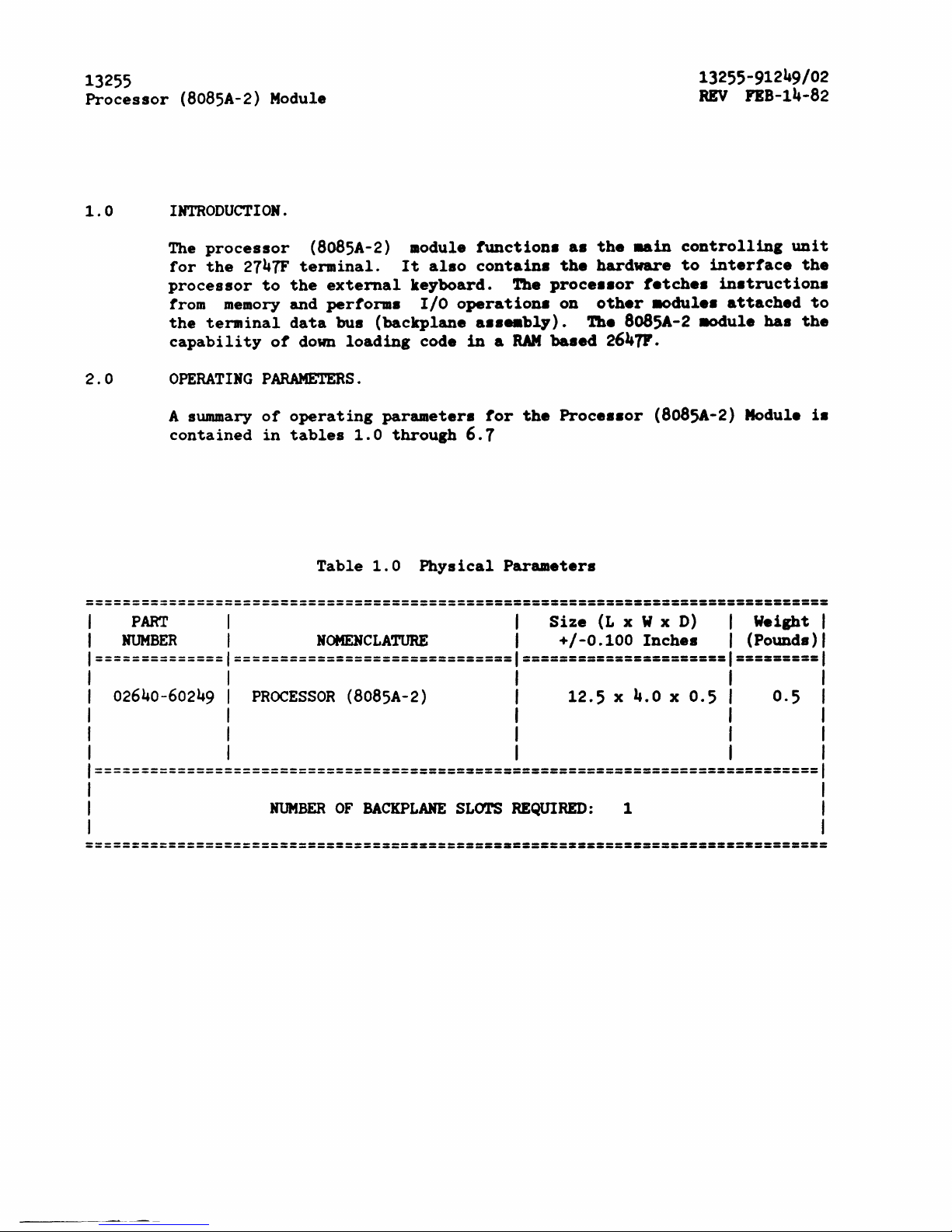
================================================================================
1
I
PART
NUMBER
1
1
NOMENCLATURE
Size
(L
x W x
1 +/-0.100
D)
Inche.
Weight 1
1 (Pounds) 1
/==============1==============================1======================1=========1
1 I 1 1 1
I 02640-60249 I
1 I I 1 1
1 I I 1 1
PROCESSOR
(8085A-2)
I 12.5 x 4.0 x 0.5 1 0·5 1
1 I 1 1 1
1==============================================================================1
I 1
1
1 I
NUMBER
OF
BACKPLANE
SLOTS
REQUIRED:
1 I
================================================================================
Page 3
HP
13255
The
information
without
HEWLETl'-PACKARD
MATERIAL,
MERCHANTABILITY
shall
consequential
or
use
notice.
INCLUDING,
not
be
of
this
contained
MAKES
AND
liable
damages
material.
MEMORY
Manual
10
WARRANTY
BUT
lOT
FITNESS
for
errors
in
connection
CONTROLLER
Part
10.
PRIM'l'ED
MODULE
13255-912q9
JUH-23-81
IOTlCE
in
this
document
OF
AMY
LIMITED
FOR A PARTICULAR
contained
TO
with
THE
1/:IS-.;2
is
subject
KIND
herein
the
WITH
IMPLIED
PURPOSE.
furnishing,
to
REGARD
WARRANTIES
Hewlett-Packard
or
tor
change
TO
THIS
OF
incidental
performance,
or
This
photocopied
Packard
document
copyright.
Company.
NOTE:
contains
All
or
Copyright
This
series
rights
reproduced
document
Technical
proprietary
are
reserved.
without
c 1982 by
is
part
Information
information
No
part
the
prior
HEWLETT-PACKARD
of
the
2647F
Package
which
of
written
DATA
(HP
is
protected
this
COMPANY
document
consent
TERMINAL
13255).
may
of
Hewlett-
product
by
be
Page 4
13255
Processor
(8085A-2) Module
1.0
INTRODUCTION.
13255-91249/02
REV
FEB-14-82
The
processor
(8085A-2)
aodule
functions
as
the
..
in
controllin,
unit
for
the
2747F
terminal.
It
also
contains
the
hardware
to
interface
the
processor
to
the
external
keyboard.
The
processor
f.tch
••
in.truction.
trom
memory
and
performs
I/O
operation.
on
other
.odul..
attached
to
the
terllinal
data
bus
(backplane
ass.bly).
'l'b.
8085A-2 lIOdule
has
the
capability
ot
down
loading
code
in
a
RAM
based
2647F.
2.0
OPERATING
PARAMETERS.
A
summary
of
operating
parameters
tor
the
Proces.or
(8085A-2) Modul.
i.
contained
in
tables
1.0
through
6.7
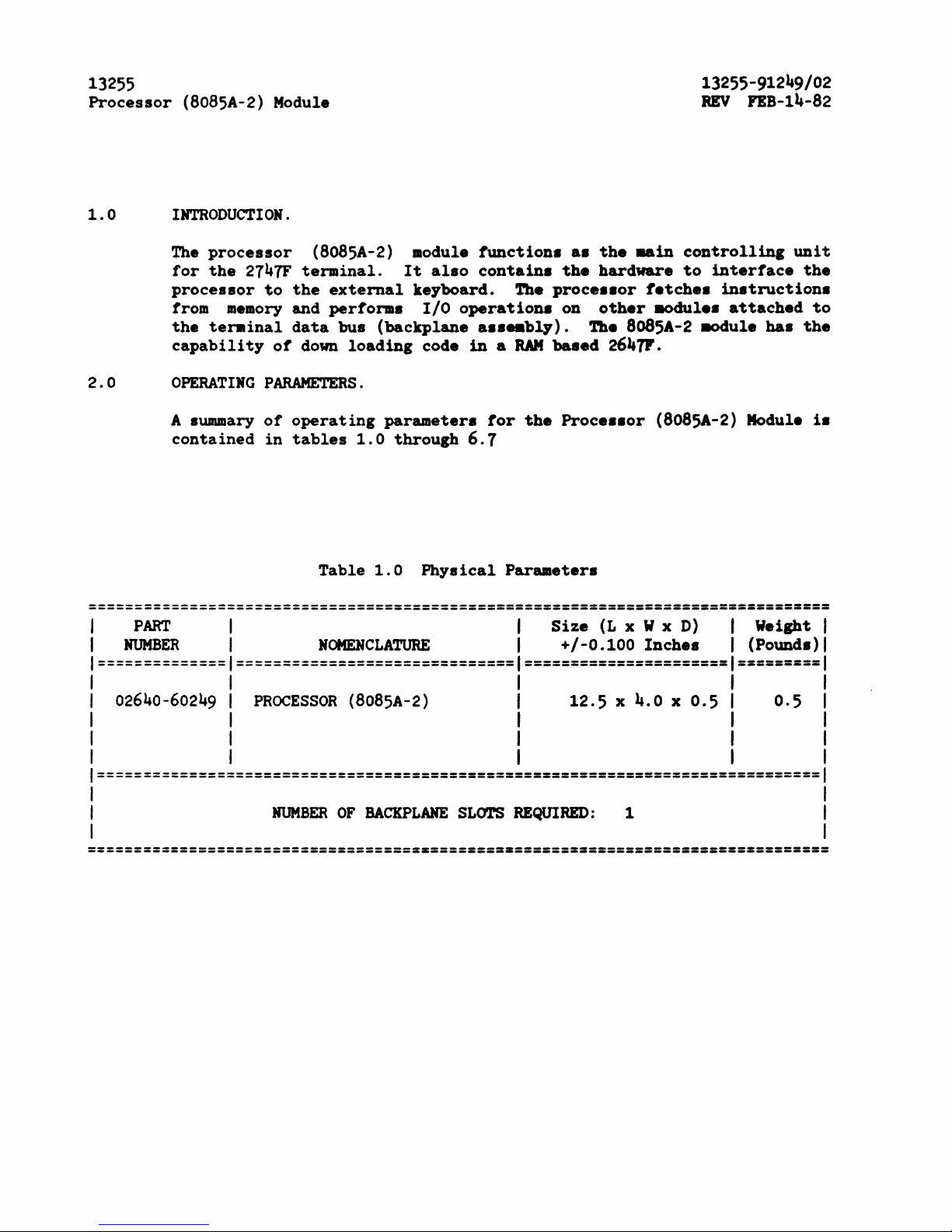
Table
1.0
Physical
Parameters
-===============================================================================
PART
1 I
Size
(L
x W x D) I Weisht
NUMBER
1
NOMENCLATURE
1
+/-0.100
Inches
I (Pounds)
==============1==============================1======================1=========
1 1 I
02640-60249 I
PROCESSOR
(8085A-2) I
12.5 x 4.0 x 0.5
I
0.5
I I I
I I I
I 1 1
==============================================================================
NUMBER
OF
BACKPLANE
SLOTS
REQUIRED:
1
================================================================================
Page 5

13255
13255-91252/03
Rev JUN-23-81
Memory
Controller
Table
2.0
Reliability
and
Environmental
Information
===============================================================================-
1
1
Environmental:
( X )
HP
Class
B
()
Other:
1
1
I
Restrictions:
Type
tested
at
product
level
,
1
1==============================================================================
1
1
Failure
Rate:
4.774
(percent
per
1000
hours)
,
--------------------------------------------------------------------------------
--------------------------------------------------------------------------------
Table
3.0
Power
Supply
and
Clock
Requirements
- Measured
(+/-
5%
Unless
Otherwise
Specified)
--------------------------------------------------------------------------------
-------------------------------------- ----------------------------------------
+5
Volt
Supply
+12
Volt
Supply
-12
Volt
Supply
-42
Volt
Supply
@
0.5
A
mA
NOT
APPLICABLE
NOT
APPLICABLE
NOT
APPLICABLE
-------------------------------------- ---------------------------------------
-------------------------------------- ---------------------------------------
115
volts
AC
220
volts
AC
A A
NOT
APPLICABLE
NOT
APPLICABLE
------------------------------------------------------------------------------
------------------------------------------------------------------------------
Clock
Frequency:
4.915
MHz
================================================================================
Table
4.0
Jumper
Definition
================================================================================
PCA
Function
I
I
Designation
I I
1=============1================================================================1
1 I I
I 1 I
1
Wl
1
RAM/ROM
Based
Terminal
(see
section
3.8)
I
I I ,
I I I
================================================================================
Page 6
13255
Memory
Controller
Table
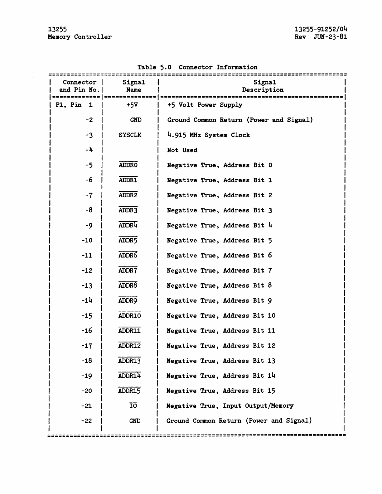
5.0
Connector
Information
13255-91252/04
Rev
JUN-23-81
--------------------------------------------------------------------------------
--------------------------------------------------------------------------------
Connector
I
Signal
Signal
and
Pin
No.
I
Name
Description
------------- --------------
-------------------------------------------------
-------------
--------------
-------------------------------------------------
P1,
Pin
1
+5V
+5
Volt
Power
Supply
-2
GND
Ground
Common
Return
(Power and
Signal)
-3
SYSCLK
4.915
MHz
System
Clock
-4
Not Used
-5
ADDRO
Negative
True,
Address
Bit
0
-6
ADDR1
Negative
True,
Address
Bit
1
-1
ADDR2
Negative
True,
Address
Bit
2
-8
ADDR3
Negative
True,
Address
Bit
3
-9
ADDR4
Negative
True,
Address
Bit
4
-10
ADDR5
Negative
True,
Address
Bit
5
-11
ADDR6
Negative
True,
Address
Bit
6
-12
ADDR1
Negative
True,
Address
Bit
1
-13
ADDRa
Negative
True,
Address
Bit
8
-14
ADDR9
Negative
True,
Address
Bit
9
-15
ADDR10
Negative
True,
Address
Bit
10
-16
ADDR11
Negative
True,
Address
Bit
11
-11
ADDR12
Negative
True,
Address
Bit
12
-18
ADDR13
Negative
True,
Address
Bit
13
-19
ADDR14
Negative
True,
Address
Bit
14
-20
ADDR15
Negative
True,
Address
Bit
15
-21
10
Negative
True,
Input
Output/Memory
-22
GND
Ground
Common
Return
(Power and
Signal)
==============-=================================================================
Page 7
13255
Memory
Controller
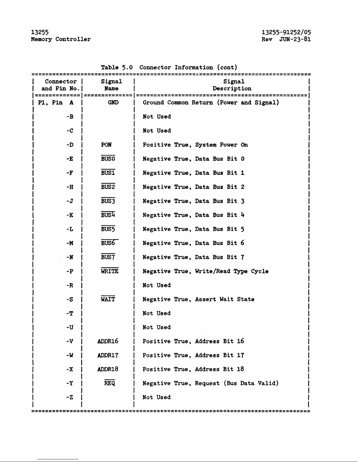
Table
5.0
Connector
Information
(cont)
13255-91252/05
Rev JUN-23-81
-----------------------------------------------.---------------------------------
-----------------------------
--------------------------------------------------
Connector
I
and
Pin
No.1
-------------
-------------
P1,
Pin
A
-B
-C
-D
-E
-F
-H
-J
-K
-L
-M
-N
-p
-R
-S
-T
-u
-v
-W
-x
-y
-z
Signal
Name
--------------
--------------
GND
PON
BUS
0
BUS
1
BUS
2
BUS
3
BUS
4
BUS
5
BUS
6
BUS
7
WRITE
WAIT
ADDR16
ADDR17
ADDR18
REQ
Signal
Description
-------------------------------------------------
-------------------------------------------------
Ground
Common
Return
(Power and
Signal)
Not Used
Not Used
Positive
True,
System Power
On
Negative
True,
Data
Bus
Bit
0
Negative
True,
Data
Bus
Bit
1
Negative
True,
Data
Bus
Bit
2
Negative
True,
Data
Bus
Bit
3
Negative
True,
Data
Bus
Bit
4
Negative
True,
Data
Bus
Bit
5
Negative
True,
Data
Bus
Bit
6
Negative
True,
Data
Bus
Bit
7
Negative
True,
Write/Read
Type
Cycle
Not Used
Negative
True,
Assert
Wait
State
Not Used
Not Used
Positive
True,
Address
Bit
16
Positive
True,
Address
Bit
17
Positive
True,
Address
Bit
18
Negative
True,
Request
(Bus
Data
Valid)
Not Used
-------------------------------------------------------------------------------
--------------------------------------------------------------------------------
Page 8
13255
Memory
Controller
13255-91252/06
Rev JUN-23-81
3.0
FUNCTIONAL
DESCRIPTION.
Refer
to
the
block
diagram
(figure
1),
schematic
diagram
(figure
2 and
3),
the
timing
diagram
(figure
4),
and
the
parts
list
(02640-60252).
The
Memory
Controller
Module
provides
program
and
variable
space
for
the
terminal.
It
consists
of
memory
drivers
and
series
termination
resistors,
data
port,
memory
array,
address
multiplexer,
refresh
address
generator,
refresh
timer,
refresh
cycle
generator,
bus
interface
and
board
select
circuitry,
and a memory
cycle
generator.
3.1
SERIES
TERMINATION
RESISTORS
The
series
termination
resistors
m1n1m1ze
undershoot
by
terminating
the
bus
lines
with
the
line
impedance.
This
approximates
to
20
ohms
since
it
consists
of
an
80
ohm
line
with
distributed,
lumped,
and
capacitive
lo~ds.
Current
limit
protection
is
provided
free
which
limits
the
driver
output
to
75
mA
if
two
or
more
array
inputs
are
shorted
together.
3.2
DATA
PORT
3.2.1
3.2.2
The
data
port
consists
of
a 74LS244
data
in
driver
(U46)
and
a 74LS373
data
out
transparent
latch.
This
port
is
enabled
whenever
BOARD
SELECT
(U53-6) and
REQ
(P1-Y)
are
both
low,
causing
U56-3
to
go low. The
direction
of
data
flow
is
arbitrated
by
WRITE
(P1-P)
in
the
following
manner:
if
WRITE
is
high,
then
U56-8
will
be
active,
resulting
in
data
transmission
from
the
Memory
Controller
to
the
data
bus.
If
WRITE
is
low,
then
U56-6
will
be
active,
and
the
data
flow
will
be
from
the
bus
to
the
memory
array.
Data
is
latched
in
the
output
latch
by
the
trail-
ing
edge
of
CAS,
the
COllunn
address
strobe.
The
transparent
data
latch
(U27)
allows
data
to
propagate
through
the
latch
prior
to
being
latched.
This
means
the
RAM
access
time
is
optimized
and
if a higher
speed
RAM
is
used,
the
memory
will
appear
to
be
correspondingly
higher
in
speed.
The
data
is
latched
so
that
completion
of
the
memory
cycle
does
not
depend on
the
completion
of
the
processor
memory
handshake.
Page 9
13255
Memory
Controller
13255-91252/07
REV
JUN-23-81
3.3
MEMORY
ARRAY
3.3.1
3.3.2
3.3.3
3.4
3.4.1
3.4.2
3.4.3
The
memory
array
consists
of
up
to
thirty-two
64K
RAMS.
socketed
to
allow
field
upgrade
and
repair.
The
RAMs
are
The power
distribution
is
via
a low impedance
4-layer
PC
board
struc-
ture.
The
ceramic
capacitors
which
supply
the
transient
current
are
organized
such
that
some
redundancy
exists.
This
allows
reliable
oper-
ation
with
one open
circuit
component.
The
memory
array
is
organized
as
four
modules
of
equal
size
(if
all
are
loaded).
The
entire
array
is
activated
by
the
start
of a memory
cycle,
which
is
when U71-9
goes
low. At
that
time,
a row
address
strobe
is
sent
to
all
four
banks.
The column
address
s"i;robe
passes
through
a
four
to
one
decoder
which
determines
which module
is
selected
for
read
or
write.
ADDRESS
MULTIPLEXER
The
address
multiplexer
consists
of
two 74LS258 quad
inverting
2
to
1
line
tri-state
multiplexers
(U75,76)
and
a 74LS244
octal
tri-state
buf-
fer
(U55).
The 74LS258
multiplexers
select
the
row
or
column
address
from
the
ter-
minal
bus
address
lines
for
memory
cycles.
Which
address
is
selected
is
determined
by
R/C
(delay
line
R12-2).
These
multiplexers
are
put
in
the
hi-Z
state
during
refresh
cycles
and
during
power
on
(when
refresh
is
occuring
continuously).
The
function
of
the
74LS244
buffer
is
to
either
transfer
or
block
the
re.fresh
address
counter
outputs
from
the
internal
address
bus.
This
buffer
is
enabled
whenever
refresh
cycles
are
occuring
(i.e.
refresh
cycle
or
power
on).
Page 10
13255
Memory
Controller
13255-91252/08
REV
JUN-23-81
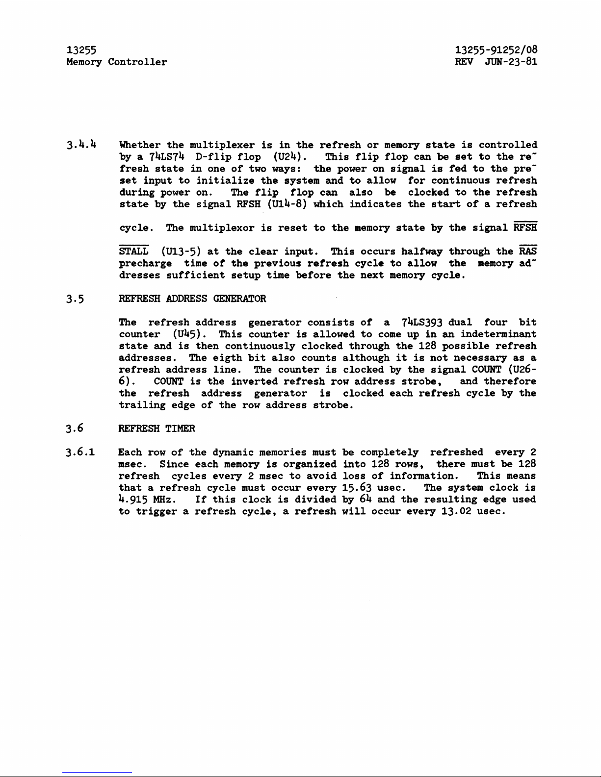
3.4.4
Whether
the
multiplexer
is
in
the
refresh
or
memory
state
is
controlled
by
a 74LS74
D-flip
flop
(U24).
This
flip
flop
can
be
set
to
the
re-
fresh
state
in
one
of
two ways:
the
power on
signal
is
fed
to
the
pre-
set
input
to
initialize
the
system
and
to
allow
for
continuous
refresh
during
power
on.
The
flip
flop
can
also
be
clocked
to
the
refresh
state
by
the
signal
RFSH
(U14-8)
which
indicates
the
start
of a refresh
cycle.
The
multiplexor
is
reset
to
the
memory
state
by
the
signal
RFSH
STALL
(U13-5)
at
the
clear
input.
This
occurs
halfway
through
the
RAS
pre
charge
time
of
the
previous
refresh
cycle
to
allow
the
memory
ad-
dresses
sufficient
setup
time
before
the
next
memory
cycle.
3.5
REFRESH
ADDRESS
GENERATOR
3.6
3.6.1
The
refresh
address
generator
consists
of
a 74LS393
dual
four
bit
counter
(U45).
This
counter
is
allowed
to
come
up
in
an
indeterminant
state
and
is
then
continuously
clocked
through
the
128
possible
refresh
addresses.
The
eigth
bit
also
counts
although
it
is
not
necessary
as
a
refresh
address
line.
The
counter
is
clocked
by
the
signal
COUNT
(U26-
6).
COUNT
is
the
inverted
refresh
row
address
strobe,
and
therefore
the
refresh
address
generator
is
clocked
each
refresh
cycle
by
the
trailing
edge
of
the
row
address
strobe.
REFRESH
TIMER
Each row
of
the
dynamic memories
must
be
completely
refreshed
every
2
msec.
Since
each
memory
is
organized
into
128
rows,
there
must
be
128
refresh
cycles
every
2 msec
to
avoid
loss
of
information.
This
means
that a refresh
cycle
must
occur
every
15.63
usec.
The
system
clock
is
4.915
MHz.
If
this
clock
is
divided
by
64 and
the
resulting
edge
used
to
trigger
a
refresh
cycle, a refresh
will
occur
every
13.02
usec.
Page 11
13255
Memory
Controller
13255-91252/09
REV
JUN-23-81
3.6.2
The
refresh
timer
consists
of
a 74LS393
dual
four
bit
counter
(U22)
set
up
as a divide
by
64.
The
output
of
this
counter
is
synchronized
with
the
falling
edge
of
the
system
clock
to
avoid
collisions
between
memory
and
refresh
cycles
(the
memory
cycle
is
synchronized
to
the
rising
edge
of
the
system
clock
by
the
processor
board).
This
synchronization
is
accomplished
by
use
of
a 74s74
flip
flop
(U71). The
synchronized
out-
put
(U71-6)
feeds
the
preset
input
of
another
74s74
flip
flop
(052)
which
acts
as a refresh
pending
latch.
The
output
of
this
flip
flop
(U52-5)
is
ANDed
with
the
signal
HEM
BUSY
(U52-8) which
indicates
if
a
memory
cycle
is
previously
in
progress.
The
positive
true
output
of
this
gate
(014-8)
is
the
signal
RFSH,
which
indicates
an
active
refresh
cycle
in
progress.
3.7
REFRESH
CYCLE
GENERATOR
3.7.1
3.7.2
The
:refresh
cycle
generator
generates
a row
address
strobe
which
is
fed
to
the
memory
chips
along
with
the
refresh
address;
the
combination
of
these
signals
performs a RAS
only
refresh
cycle
for
the
memory
array.
The
cycle
is
triggered
by
the
signal
RFSH,
inverted
and
presented
to
the
clock
input
of
a 74LS112
J-K
flip
flop
(U26).
This
flip
flop
is
tied
to
a
permanent
set
state.
Setting
this
flip
flop
causes
the
K
input
of
the
other
half
of
u26
to
go
high
resulting
in
the
toggle
state
at
the
inputs
of
this
flip
flop
(U26-2,3).
The
next
rising
edge
of
the
clock
causes
signal
RFSH
RAS
to
go low;
it
will
remain
so
for
one
en-
tire
clock
cycle
(204
nsec).
Two
74LS74 D
flip
flops
(013,23)
extend
the
refresh
cycle
by one more
complete
clock
cycle
to
allow
sufficient
RAS
pre
charge
and
address
setup
time
as
discussed
above.
U23-5
feeds
bac:k
to
the
refresh
timer
to
end
the
cycle
and
allow
a new
timing
cycle
to
begin.
During
power
on,
the
signal
RESET
forces
u26
to
the
toggle
state
perma-
nently,
resulting
in
continuous
refreshing
until
RESET
returns
to
the
high
state.
Page 12

13255
Memory
Controller
13255-91252/10
REV
JUN-23-B1
3.B
3.B.1
3.B.2
3.B.3
BUS
INTERFACE
AND
BOARD
SELECT
CIRCUITRY
The
bus
interface
circuitry
consists
of
several
buffer
drivers,
a
wait
state
generator
and
an
10
port
designed
to
be
used
by
OEM's
for
soft-
ware
protection.
The
bus
signals
SYSCLK,
REQ,
and
PON
are
buffered
by
74LS244
drivers
to
reduce
loading.
In
addition,
SYSCLK
and
REQ
are
also
inverted
to
be
used
in
that
state
by
the
timing
circuitry.
The
Memory
Controller
Module
requires
one
additional
wait
state
be
add-
ed
to
the
normal
bus
cycle
in
order
to
provide
sufficient
time
to
ac-
complish
memory
reads
and
writes.
To
add
this
extra
state,
a
wait
state
latch
is
used.
This
latch
is
a 74LSl12 J-K
flip
flop
(U44).
This
flip
flop
is
set
by
(071-9),
which
signals
the
start
of a memory
cycle
and
is
cleared
by
CAS,
the
column
address
strobe.
This
timing
results
in
the
addition
of
one
extra
wait
state.
WAIT
is
driven
on
to
the
bus
by
a 74s03 open
collector
NAND
gate
(U42-3).
The
Memory
Controller
Module
incorporates
a
feature
which
will
allow
any
interested
party
to
protect
his
applications
software
on
the
2647F
by
providing
space
for a four
byte
code which
can
be
burned
into a 32xB
PROM
by
the
user;
this
code
can
be
used
to
encrypt
the
applications
software
by
any
number
of
algorithms.
U41
is a socket
for a 32xB
field
programmable
PROM
(Harris
7603
or
equivalent).
The
four
byte
code
can
be
accessed
by
reading
10
ports
BAOO,
BA02,
BA04,
and
BA06
(hex).
The
codes
will
appear
to
the
processor
to
be
the
inverted
state
of
what
is
encoded
in
the
PROM.
Page 13

13255
Memory
Controller
13255-91252/11
REV
JUN-23-81
3.8.4
The
board
select
circuitry
combines
the
state
of
two
of
the
three
most
significant
bus
address
lines,
ADDR16
and
ADDR18,
as
follows:
Table
6.0
--------------------------------------------------------------------------------
--------------------------------------------------------------------------------
ADDR18
ADDR17
ADDR16
FUNCTION
0 0 0
Code Page
0
0
0 1
Unused
0
1
0
Code Page
1
0 1 1
Unused
1
0
0
RAM
Space
for
Variables
1 0 1
Unused
1 1
0
RAM
for
BASIC
Workspace
1
1
1
Display/IO
Space
-------------------------------------------------------------------------------
--------------------------------------------------------------------------------
3.8.5
As
can
be
seen
from
the
above
table,
a RAM-based
terminal
would
have
to
respond
to
all
four
cases
where
ADDR16=0;
a ROM-based
terminal
needs
to
respond
to
the
two
cases
where
ADDR18
and
ADDR16
=10 . When
jumper
W1
is
absent,
the
output
of
the
AND
gate
(U14-6)
passes
the
inverted
value
of
ADDR18.
This
gets
combined
with
the
value
of
ADDR16
to
generate
MEMGO
(U42-6).
It
is
also
combined
with
10
to
generate
BOARD
SELECT
(053-6)
which
is
used
to
enable
the
data
port
and
to
enable
the
row
and
column
address
strobes
to
the
memory
array.
When
W1
is
present,
u14-5
is
tied
to
ground,
therefore
the
output
of
the
AND
gate
(U14-6)
is
permanently
low.
In
this
case,
MEMGO
and
BOARD
SELECT
depend
only
on
the
value
of
ADDR16.
Page 14

13255
Memory
Controller
13255-91252/12
REV
JUN-23-81
3.9
3.9.1
3·9·3
MEMORY
CYCLE
GENERATOR
The memory
cycle
generator
is a synchronous
sequntial
state
machine
composed
of
several
flip
flops
and
gates.
The
purpose
of
this
state
machine
is
to
generate
the
row
and
column
address
strobes
for
memory
cycle
operations
with
the
appropriate
timing.
A
memory
cycle
begins
when
HEMGO
goes
low.
This
is
synchronized
with
the
leading
edge
of
REQ
by
a 74s74
flip
flop
(071).
This
also
accom-
plishes
the
rising
edge
clock
synchronization
mentioned
above
in
sec-
tion
3.6.2,
as
REQ
is
synchronized
with
the
clock
by
the
processor.
The
output
of
this
flip
flop
(071-9)
represents
a
memory
cycle
pending.
This
signal
is
ANDed
with
RFSH
to
prevent a memory
cycle
from
starting
while
a
refresh
cycle
is
in
progress.
The
output
of
this
gate(Ul5-6)
indicates
an
active
memory
cycle.
The
leading
(negative)
edge
of
this
cycle
active
signal
sets
HEM
BUSY
to
the
true
state,
thus
the
start
of
any
refresh
cycle;
it
also
clocks
a 74LSl12
preventing
flip
flop
which
starts
MEMRAS,
the
row
address
strobe
(Ul2-12).
Two
flip
flops
(U13
and U25)
then
maintain
HEMRAS
in
the
low
state
for 2 clock
cycles
(408
nsec).
The
output
of
the
second
flip
flop
(U25-9)
is
the
column
address
strobe,
CAS.
It
lasts
for
one
clock
cycle
(204
nsec)
and
fol-
lows
the
leading
edge
of
HEMRAS
by
204
nsec
subject
to
logic
delays.
As
with
the
refresh
cycle
generator,
two 74LS74 D
flip
flops
(U21)
are
used
to
extend
the
memory
cycle
to
allow
for
RAS
pre
charge
time.
The
output
of
the
second
of
these
(U21-5)
resets
HEM
BUSY
to
the
false
state,
thus
ending
the
memory
cycle.
MEMRAS
is
ted
to a delay
line
(HP
part I 1810-0384,
50
nsec
delay,
taps
at
10
nsec
intervals)
where
it
is
delayed
40
nsec
to
become R/C,
the
signal
which
determines
which
halt
of
the
address
is
fed
through
the
address
multiplexers
(see
section
3.4.2).
Page 15
13255
Memory
Controller
13255-91252/13
REV
JUN-23-81
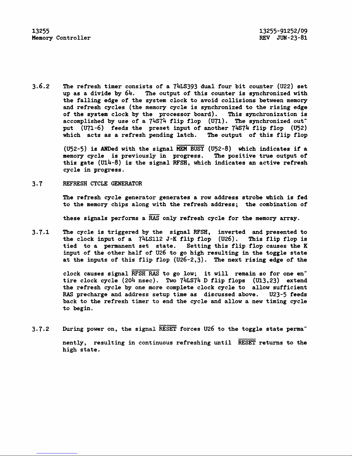
3.9.5
MEMRAS
row
address
latch
memory
line
(Ul7-2,1)
cessed.
other
puts;
module.
data
decoder.
enable
is
is
this
ANDed
strobe
out;
being
to
When
input
pulse
with
BOARD
signal
in
addition,
addressed.
This
decoder
determine
the
decoder
(U17-5)
is
used
SELECT
to
the
This
uses
which
is
produces a similar
as
the
the
memory
CAS
is
is
accomplished
ADDR18
ot
the
enabled
column
ORed
array
used
and
tour
by
address
with
RFSH
(Ul4-11).
to
determine
with
ADDR17
memory modules
BOARD
SELECT,
pulse
strobe
RAS
a 74LS138, 3
at
the
at
one
for
to
CAS
which
address
is
a
CAS
ot
the
torm
is
used
module
being
at
four
accessed
the
to
ot
to
pins
acthe
out-
8
Page 16

<
W~IT
I
I
c..L.K
5
V"-,t...
I.. ;:.
"
""
CoL
K'
DON
.....
6v
t
'S
I
/'
WKII~
~
IkJiERFAC.E
8QDRl'O
I
Arvo
i
I
HOD
KI7
I
'"
i\
'fLEe1
UlJ
I"·
v
I
I
(i
i((lJ.
(\{('Y
I
I I
\
I I
V
BvA
R .)
V
(J
SEU=:CT
wr
.....
1
I
/1
v
IV
!
I
I
I
BLtS Df\1 A
k
6/
I
I
/
I
I
B/
"-
/
~
/
/
dl
.::
7
/
ktS
AOORESS
Li:xE..K
8/
REFRE'S1-1
I
AOD
RESS
/
'\
I
G£l-E~p..(o«.
I
.
'----.
1
l,.-
I-
i.-
I
-
iVI
£
11'\
oR
Y
( '(CLE
/
I
I
I
GEfJf
R
I\1
0
R.
,
I
I
I
~
'"
I
RilS
c..AS
,I,-
----
'(
1~
j tOu
tv"
,
I
J"
[l{1
Em
BUS\(
-
/
I
i
i
I
I
I
i
I
I
I
i
I
I
I
ili
R E
r=
F<
ES
+i
,/
II~,E~
I
RtFRES~
CYCLE
GENe
RATO£.
FIGURE
1
02640-60252
BLOCK
DIAGRAM
JUN-23-81 13255-91252
Page 17
I 5/1
,---------
________
~~;-q
Ull
p'-12https://manualmachine.com/'1.~'£=I'1~R~A~5
__
____j
~-o~~P~aN~--~~~--~~~-------------------------'----------------------,,~~~--T----+------~--
~----
__ ~ __
~~
U72
/..j2'1Lf_
PI-rt;>~R~£~G~--------------------------~~8~£Q
I
+SV
U71(
~R2
7'fALS~'I
'(.71f
~~
PI-X....-
v-
~
o
I
I
I
WI
o
PI-V
)~-=AD=DR=''''-b
____
'V
___
...LOO..Q
W I /1
RI
2
Al
n/c
Z
A2.
2
,413
PI-5
"511
RFSH
2 Al.
N
~~
I'
fir
PI-21
I>.=--=O=------------4.>-----;-=c..-----------~
L'
'"'M=EM'-'=OR'"'"Y-:.C=rc=~£=__=(;=~=N=CIf=A""'TO=1I
_ _
__
I
~
~~'3
LSI~
L532
1~~~~=rD-~~=l-
____
~---·s-v---~------_t----------------r_------------
___________________
r_---J--_t-------------------------~BO~A~R~D~S~C,~L~CC~T~~~~~)
PI_I'f~ADD,.C;
-'-"-~
,
2,
USJ
'
2-
~~
b - 2
A1
~Ab;;hR;/~o~---------.
~-----------~ y~
~
..
.---_+-------+_-----~_+----------+_-----------------+_---_+
___ ~ _________________
~
PHS I L532
...-
~
P"/i,t;>
AlJDRII
~
8
PI-tt
I>
ADlJR'f
~
'---
_____
-L~
AD
DR!
PI-6
~
ADDR2
PI-N
PI-7t;>~A~DD~R~Z~
_______________________
.--'U·~7~4~-----------
-------~------~-------~---------~-----------------------------~r_------~---------------~~~~~~
t-'----------::==;----i~
PI-n
'(Ag~8Lfc-L~r--------------------,
PI_]
c:>-"'-S.:..:YS".,L.,..,L:..cK'--
_____________________
r-t1
'
II,
cal
-Hr>=--~'-;-------·--·-------+----+----------
I
I
I
I
I
I
I
I
R~
If(
L
I
__
__
UlbI-9.<..-
____________
--+---f
ReFReSH
CYCLe
{.CNI!/MrOI!
2 1
U71f
7'fALSfI'I
PI-L
P/-K
I-:'--------------'!:~~--!:>
"'-
J
r-----------===='O----i·~P/-
H
F-----------""""====;;---!:>PI-F
a,JI-"-------------==='---t:::>
PI-€;
32-8
ROM
L-
____________________________________________________________________________________________________
~R
~r~~~s~M~LL~
________________________________________________________________________________________
~tr~~~
R~AS~
L-________________________________________________________________________________________
_
________________________________
~CO~U~N~T
__
~
NOTES:
I, ALL
RUI.!
TDRS
ARC
IN
OHMS_
Z.
VR3
INDICArES IVODE
PI)LL£D
TO
'SV
THROV£.H
VR1, A
It
RUISTOR
•
.3.
"?jR£F£RS
TO
A IVODE
OIV
THE:
TIMING
DIAGRAM_
FIGURE
2
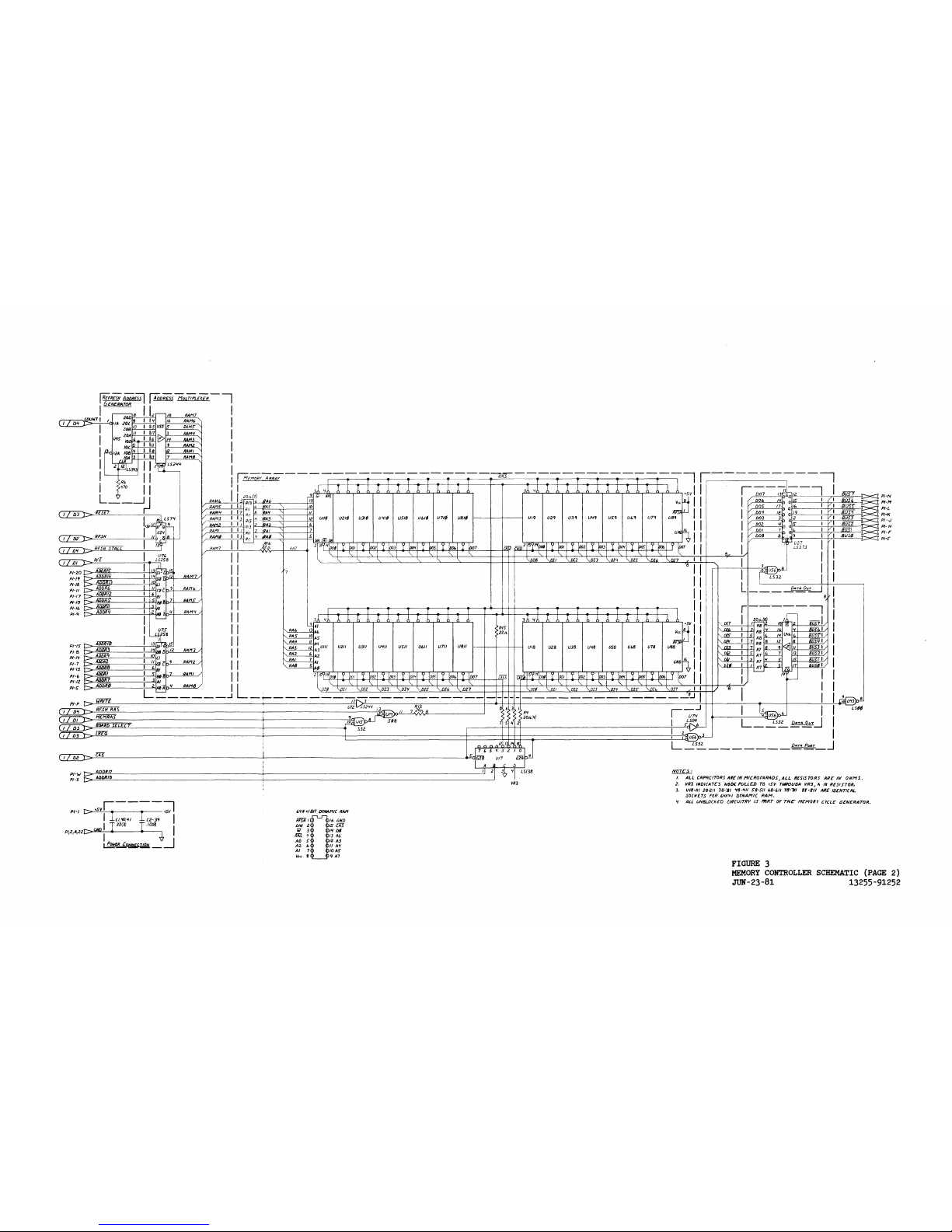
MEMORY
CONTROLLER
SCHEMATIC
(PAGE
1)
JUN-23-81 13255-91252
Page 18
~R£SH
AL>DR~
[AQoR£"SS
MtlLM£m-1
I
GCNERATOR I I
~B
2-18
RAM 7
( I /
D~
(OUNT
'I
t
104
ZQ£
9 I I
'f
16
IIAI16
2GB
10
I
115
ClSS
l5
RAMS
lOA
/I
I
'"
f'.>...
3 RAM'!
I (J'fS
IG
(, I 16
Villi
1tAM3
,~(.
5 I
1/1
,
RAMi!
I
P<>2A
/Q8
1
'f I
18
IZ
RAMI
¢
/QA
[3 I 1/3
7
RltM~
I I
I/WTr
~4
Z
12
L5J93
U.
I
~1I6
II
i
i~70
II
L
__
--.J
I
RESET r
(1/
D3
T-
~~~u-
______
~I~L~~~~"~~R~A~M~'f~
I~
I
U7S
l
2S8
I
13
IS
~
D----'=~~------____;I:_'I..!...'fIDll15
1£
RAN]
I
10
£1
=>---=:::=:==:::-----------7-'
-"'-IS
BffB
7 RAMI /
I
~AI
RAM7
D--"""""!Z!!.---------I;-.IO..jA2d A
'I
R",MtJ
L:::::.
_____
...J
''fk~/BJT
DYNAMIC
RAM
RFSH
'016
GND
biN 2 IS
CAS
W 3
1'1
DI
m If
13146
140
~
12
A3
A2
b
/I
A'f
AI
7
10
AS'
Vc<
II
.,
A7
BUS 7
~
8llS6
BUSS
i""::::oc::::"
BUS'1
i::>c:::::"
B()S3
i"::><::"
BU~2
r--
--
Bu.s!
;:::-
:::
BUj~
~
-
-
~_8
~U'fJr
LS~
NOTE5:
t.
ALL
CAPRClTOR5
AftE
IN
f'r1C.ROFARADS,
ALL
RESISTOR5
ARE'
IN
OHMS_
2_
VR3
INDICATCS
NOM
PULLE:1J
r(J
ti"V
TIII1OU611
,(R3,
A
It
RESISTOR.
3.
V18-111
28-211 38-311
'f8-'0/
SS-Sll
68-'"
7tJ-711
,,-'"
ARC
IDENTICAL
.sOCkETS
FOR
'"K""
DYNAMIC
RAM.
1(.
All
UNBL.J)'kED
"ReUITRY
15 fI/fII!f.T
OF
THe
I'1EMORT
C.YCLE'
6CNCRATOR.
FIGURE
3
PI-N
Pf-,.,
PI-L
PI-K
PI-')
PI-/-I
PI-r
PI-e
MEMORY
CONTROLLER
SCHEMATIC
(PAGE
2)
JUN-23-81 13255-91252
Page 19

ME.M
RA~
~"'s
TO
MHI\O~Y
O~
CONTIl.OL.L!~
C.A~
TO
MeMO':'!'
ON
CONT~OL.Lcll.
RI=~
(ME.M
&U~"I'''l)
IZF~i-I
?TALL
I-------'----.J-
_ ll±!...
__
_
'---_-..:..".:....."--_-_-_''--
__
-L..
__
!!~.
_____
J
I---------------~------~---,~
r--~~-~4rr_----------------_1»
LI
..,:4.;..'.=-.JIc..l
I
.;..A.:::!..5::..:'
__ 4 ________________________________
-'1
__
1.02~
__
__
il
J
---------------------I+-----------r-I+-+-S-74-.L~:~'-Iv.v=~~+-L-S-~-
B-~-~-74------------------------------------------------------~1
I
1L-_7_0
__ -__
'~!\V~I~._?_~Z
__
._~_'1_2
____
~1!4~~~_'J~CA;~Ar-.7L7~7~S~+~S~II~2------i
~~==~-P-~-E-C-H-A-IZ-~-~------------------------------1~
...
204
"'I
---l-"1e
- -
-:
h
511
r,7S-.JTI-;;;rn=--
..
-=S=-=7:-:4-------t------------------------jJ/
I I
\
I 1 I
~----------------~--------~i
__
~--~--,
\
~40!2~
~40
~
W
-----------------~-----
ll~l
AL~'4-'"
S:
12
,r"'r-------------+-------------------------i,1
l~'~~
________
~~
\
I
4~-
'ALS,.4
...
Lo;74
Ir_7~71_"Tj----t-----------------------iJ
\
Jl
....
1
_S_s-_--'1_L_?_24_4_+
_L_~7_4
___
~I,_4
_,,_
~
rl~~z~J----------------~~
1-----------------------------+-------.
L
-
4
.'5
-,
CAS
+
l?I't.
1'2~9~Jr-------------------------~1
~
112
---i
DIZ.lVE.12.
~"~:'OOM
,..
' I
,,1:.0,";;:
<£,j
DATA
IN
~e7
-I
Acc.e",~
TIME.
1=12.0M
I2.A':>
1~2.:::e'u.....:A=L.:::~P~4~+.:::2_X.:...57_4_
...
_5~¢_e
_______________________
-JI
__ ~ __
j~tS74+5~8
IL2::.:"=-...,~A_L._S_'_¢_4_._L._5_'I_e
_________
II_Z~
J
AL.
'"
~4
..
L5112
1L-~_-_-~i_A_L_':>_~_4_+_L._S_7_4
___
~lr,_~~_~I'J-A~L~~~_~4~+~L~S-74~----~~
L'--...:;-5...:8'----
....
'_l5_2_4_4_+_L.~_74
____
,I_
~"_
-'
LS244
+ LS74
NOTE,,):
I,
ALL
TIME';
IN
~ANO'>ECON~,
2.
...
INDICAT!05
PIZOCE:~~O~
DELAY.
ALL
OTH~~
DE.L.A.Y~
ARE:
DUe.
TO
ON~BOAIl.O
LO~IC..
3.
OuTPuT
DATA
LATCHE.D
OI=F
&OAR-D.
ll,.
'iZ./~
i~
IIIIEMI4A~
T"I<Ooo
..
A DE.L.,l.Y LINE.:
IF
IIIIEM12.A5
I':>
':>LOW,
';<./C
WILL
f'>E.
5LOW
AND
V15E..
VEl2.o::.A,
';.
COLUMt-J
ADDRE55
AVAILA~L!.:
24-,,~
AnE.R ,;u.s EARL.IE.';T,
4Zn~
AFTc~
I2.A5
LATE~T
0"-1
CONTROLLER
f>OARD.
76n~
AHE.12.
';<.AS
LATE5T
0'-1
ARRA"l'
E>OAIl.O,
FIGURE
4
MEMORY
CONTROLLER
TIMING
JUN-23-81 13255-91252
Page 20
3
o
o
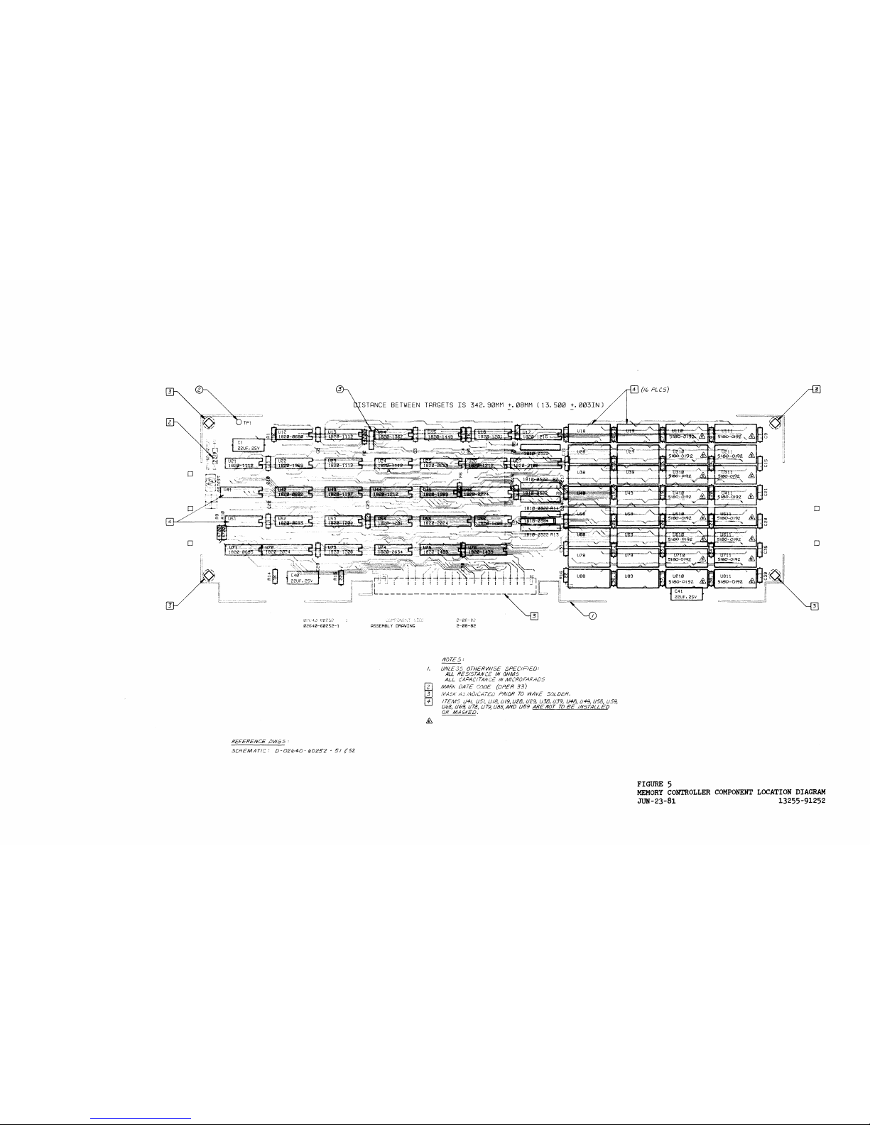
02640-60252-1
R£~EREtYCE
OW65
;
SCHEMATIC:
D-02G4{)-/h02S2
-
5/
(52
BETWEEN
T~RGETS
IS
342.
90MM
+.08MM
(13.500
+.003IN)
ASSEMBLY
DRAIJING
I.
2-08-82
NOTES;
UNLE
35
OTHERWI5E
SF'ECIFIED:
ALL
RESIST.4#CE
IN
fJHM5
ALL
CAPAOTAlrCE
IN
MICROFARAf)S
MARA
DATE
('!JDE
(OPER
33)
(AIIASK
/1.:;
iiV[)ICA,Ei.J PI?t{)R
TO
WAvE
SDLDE:R.
ITEMS
U41(
U5/,
/.J18,
LJ/9,
LJ28,
U29, U38, U39,
U48,
U49,
U58,
U59,
UIbB,
Ll69, U7B, U79, UBB,A.ND
U89
ARE
NOT
TO
BE
1#5
TALL
ED
OR
MASKED,
FIGURE
5
~-=======----=::---
..
- -
(---
\ I
'"
•
C)
\ .
.-7
;1
II
Ii
i!
Ii
Ii
o
o
MEMORY
CONTROLLER
COMPONENT
LOCATION
DIAGRAM
JUN-23-81 13255-91252
Page 21

Replaceable
Parts
Replaceable
Parts
Reference
HP
Part
c
Qty
Description
Mfr
Mfr
Part
Number
Designation
Number
0
Code
02640-602~:;2
4
RAM
CONTROU._FR, PCA
28480
02640-602S?
Cl
0180·-2879
7
3
CAPACITOR-FXD
2?UF+50
··10X
<·:~W1)C
AI..
2134130
0100·_·2879
C~>'
o
160-4~j57
0
3B
CAPACITOI~"'FXD
.1UF
+-,20%
SOVDC
CER
16299
CAC04X7RI04M050A
C3
0160-4557
0
CAPAr:ITOR-FXD
.1UF
t··20"
50'J'OC
CE.R
16~>'99
CAC04X7RI04H050A
C4
0160-4:':;57
0
CAPACITor~-FXD
.1UF
+"'20%
SOVDC
Cr.R
16299
CAC04X7RI04M050A
C5
0160-4~,57
0 CAPACITOR-·FXI>
.1UF
-to
..
·<!O"
50V'OC
CE'R
16:'.99
CAC04X7RI04H050A
C6
o
160-4~j57
CAPACITOR-FXD
.1UF
+·_·20::1.
50VDC
CER
16299
CAC04X7RI04M050A
C7
11160-4557
CAPACITOR·_·FXD
.1UF
t···20"
50VDC
CER
16;''.99
CAC04X7RI04H050A
Cf.J
o
160-4~j57
CAPACITOR-FXD
.1UF
+
....
20"
50VDC
CER
16;?99
CAC04X7RI04MD50A
C9
0160--4557
r:APACITOR-TXD
.1UF
t···20:1:
50VDC
CER
16299
CAC04X7RI04H050A
C10
o
160-4~:;57
CAP
AC
ITOR
-F
XD
.1UF
+·-·20"
SOVDC
CER
16?99
CAC04X7R104M050A
Cll
0160-4557
CAPACITOR
..
FXD
• 'IUF
+
....
;:!II"
SOV'OC
CER
16299
CAC04X7R104H050A
C12
0160-4:':;57
CAPACITOI~
-FXD
.1UF
+-·20"
50VDC
CER
16299
CAC04X7RI04M050A
C13
0160-4557
CAPACITOR-·FXD
.1UF
+,,20"
50'JDC
CE.R
16299
CAC04X7RI04H050A
C14
0160-4557
CAPACITOR
-FXD
.1UF
+-,20"
SIlVDC
CER
16299
CAC04X7RI04M050A
C15
0160--4~;57
CAPACITOR-FXD
.1UF
t·_·<.!O'X
50'JllC
CER
16;:.~99
CAC04X7RI04H050A
C16
o
160-4~j57
0
CAPACITOR-FXD
.1UF
+
....
20::1.
SIlVDC
CER
16299
CACIl4X7R104M050A
C17
11160-4557
0
CAPACITOR-FXI>
.1UF
-t
....
20"
50'JI>C
CER
16::!99
CAC04X7R104H050A
C18
0160-4:7;57
0
CAPACITOR-FXD
.1UF
+
....
2 or.
SOVDC
CER
16299
CAC04X7RI04M050A
C19
0160-4557
0
CAP
j!.C I TOR -..
FXI>
.1UF
t
....
::!O"
50V'OC
CER
16<.'99
CAC04X7Rl04H050A
C;?O
0160-4S57
0
CAPAC
ITOR
-F
XD
.1U.
+-20"
SOl-'DC
CER
16299
CAC04X7RI04M050A
C21
0160-4557
CAPAr:ITOR
--FX'O
.1UF
~""20'X
50'.'ilC
CE.R
16299
CAC04X7RI04H050A
C;:~2
0160-4S57
CAPACITOR-FXD
.1UF
+
....
20"
50VDC
CER
16299
CAC04X7Rl04MOSOA
C23
0160--4557
CAPACITOR-FXI>
.1UF
t···20"
SO'JDC
LE.R
Ih299
CAC04X7RI04HOSOA
C;''.4
0160-4557
CAPACITOR·-FXD
.1UF
+·-·20"
50VDC
CER
16::!99
CAC04X7RI04M050A
C25
11160--4557
CAPACITOR-rXll
.1UF
+'''20'X
SOVDC
CER
16;::99
C~C04X7Rl04HOSOA
C~>'6
o
160-4~;57
CAPACITOR-FXD
.1UF
+,-20"
50VDC
CER
16299
CAC04X7RI04M050A
C27
0160·-4557
CAPAr;ITOR-FXI>
.1IJF
+,,23"
50'JDC
CE.R
16<'.99
CAC04X7RI04H050A
C;;'.8
o
160-4S57
CAPACITOR-FXD
.1UF
+·_·20r.
SOVDC
CER
16f.~99
CAC04X7R104M050A
C29
0160--4557
CAPACITOR-FXil
.11JF
·~""20r.
50'.'I>C
CER
16<.'99
CAC04X7RI04H050A
C:~O
01(,0-4557
CAPACITOR-FXD
.1UF
+·_·20"
50VDC
CER
16299
CAC04X7RI04M050A
C31
0160-4557
CAPACITOR-FX'O
.1UF
+",20"
50'.'ilC
CER
16<"99
CAC04X7R104H050A
C:52
0160-4::;57
CAPACITOR-FXD
.1UF
+·_·20"
SOVDC
CER
16299
CAC04X7RI04M050A
C33
0160--4557
CAPAC I
TOR
-rXI>
.1UF
t·
..
20"
50VDC
CE.R
16<~99
CAC04X7RI04HOSOA
C34
0160-4::;57
CAPACITOR-FXD
.1UF
+,-20"
S(lVDC
CER
16299
CAC04X7RI04MOSOA
C35
0160-4557
CAPACITOR-TXD
.11.lF
+·,20"
50VDC
CE.R
16299
CAC04X7R104H050A
C:56
0160-4::;57
0
CAPAC
I
nw
-FXD
.1UF
+·_·20%
50VDC
CER
16299
CAC04X7RI04M050A
C37
0160--4:7;57 0
CAPACITOR-FXI>
.1UF
+,,20"
50'JDC
CER
16,!99
CAC04X7RI04H050A
C38
o
160-4~;57
0
CAPACITOR-FXD
.1Ut
+-20r.
SOVDC
CER
16299
CAC04X7R104M050A
C39
0160-4~;57
0
CAPAr:ITOR-FXD
.1UF
-t·-20"
50'.'DC
CER
16,:99
CAC04X7Rl04H053A
C40
0180-21379
7
CAPACITOR-FXI>
22l.JF+50-10'X
2~,VI>C
AI..
284BO
0180
'-2879
C41
0180
-·2879
7
CAPAClTOR-FXI>
2<.'UF+50"·10r.
2~;VDC
/!,L
28480
0180-2879
R1
0683-1025
9 4
RESISTOR
11(
5i:'
. .
25W
FC
TC=·-400/+f.,OO
01121
CHl025
R2
0683-4725
2 3
RESIGTOR
4.'?K
~J~
.25W FC
TC=--400/+700
01121
C94725
R3
0683-1025
9
RESISTOR
1K
S%
.2SW
FC
TC=-400/+600
01121
CB1025
R4
11310-0322
9 5
NETWORK
-·RES
Il·~np20.
0
OHM
X 4
01121
40139200J
R~5
0683-1025
9
RESISTOR
lK
5X,
.25W
FC
TC=--400/+600
01121
CBI025
R6
0683-4715
0 REGIGTOR 4'70
~j%
,2~;W
FC
TC=·400/+600
01121
eB4715
R7
1810-0:322
9
NETWORK·-REG
B-SIP20.0
OHM
X
4
01121
40f.lFl200J
R8
1810-,,0322
9
NETWORK·_·RES
0
·~3IP20.
0
OHM X -4
31121
4089200J
R9
0683'-4'725
2
RESISTOR
4.7K
~jl't
.25W
Fe
TC=-40
0
/'~70
0
01121
CF.l47:?5
RI0
0683-4725
2
RESISTOR
4.
'?K
!"iX . 2!':',W
FC
TC=·-40
0/+70
0
01121
C94725
Rl1
un
0-0322
9
NETWORK
'-R
E~:;
8·
..
8YP20.0
OHM
X 4
01121
4CBFl200J
R12
1810-0384
3 DEl.
AY
L.INE
TOTAl.
DELAY:
50
NS
<TAPS AT
01961
20666
R13
H110-0:322
9
NFTWORK·-RES
881P20
• 0
OHM X 4
01121
4013F.1200.T
R14
0683"'1025
'7
RESISTOR
11(
~,%
,?5W
Fe
TC=-400/~600
(l1121
CItl025
R1S
06B3-2;;!05
9
;~
RFSISTOR
2;~
5i!.
•
;~~jW
FC
TC=-AOO/+500
011?1
CFt2205
R16
06133-,2205
9
RESTf:>TOR
2;>.
:';%
.
~.~~iW
FC
TC=-AOO/I'500
()1121
CB2~~n5
TP1
0:360-0S35
TERMINAl..
TFST
POINT
PCB
00000
ORDER
BY
Dl'nCRIPTION
ll12
1820--0606
9
1
IC
GATE
TTL.
S
ANI)
TPI...
3
..
HIP
01295
!:;N74!311N
1.I13
H120-1112
8 4
IC
FF
TTl.
LS
D
..
·TYPE
PllS"-[DCF:--TR
Ie
01295
SN'74LS74AN
1.J14
18<.'0'-1367
5 1
IC
GATE TTL. B
ANI)
QUAI> 2 HIP
01295
!3N74S08N
1.115
H120-1449
4 1
Ie
GATE
TTl.
S
Ot?
QUAD
2"·JNP
01 ;:'95
8N'74832N
L116
11320-1201
6 2
IC
GAlE
TTl.
l.B
j!,NI>
QUAD
;.,
",I'll'
31295
SN74LS08N
1.I17
1f:120-1216
3
Ie
DenR
TTI_
L8
3
·TO
..
·-8
..
·LJNF
3"-INP
01295
SN'741.8138N
U21
1020-·1112
8
IC
FF
TTL
LS
1).,
YPl'.
POS-··EDGE"·TRT.G
01295
SN74LS74AN
1.I22
1020-1989
7
.,
IC
CNfR
TTl...
LS
BIN
DUAL
4
....
BIT
07263
741..8393PC
1J23
18i.'0··1112
8
IC
FF
TTI._
I
..
S
1)-.,
YPt::
POS-E.DCE-
..
TRIG
01i'.95
SN741..S74AN
U24
1f:l;~0-1112
8
Ie
FF
TTL
l..S
D-TYPE
pnS-'ED(~E:-TRIG
01:'.95
SN'74L87-4AN
Page 22
Replaceable Parts
Reference
HP Part
c
Qty
Designation
Number
0
1.)25
1820····0629
0
1.126
11:120-1212
9
2
1.)27
1820-2102
8
1.142
1£:120-0682
5
1I43
1820'-'11'n
9
1.144
1820-1212
9
\J4!'i
1820-1989
7
1I46
1820-2024
3 3
LJ52
1820-·0693
B 2
l.I53
18;,!0-1202
7
US4
1820-,1201
6
l.I::iS
1820-2024
3
U56
18i.'O-1208
3 2
1.I71
1820-0693
8
U72
1820-,2024
3
l.I73
1820-1~~08
3
U74
1820-2634
1
U7S
1f.120-1439
2
2
LJ76
1820·_·1439
2
1'!!':i1·-0697
5
2
ei180-0192
16
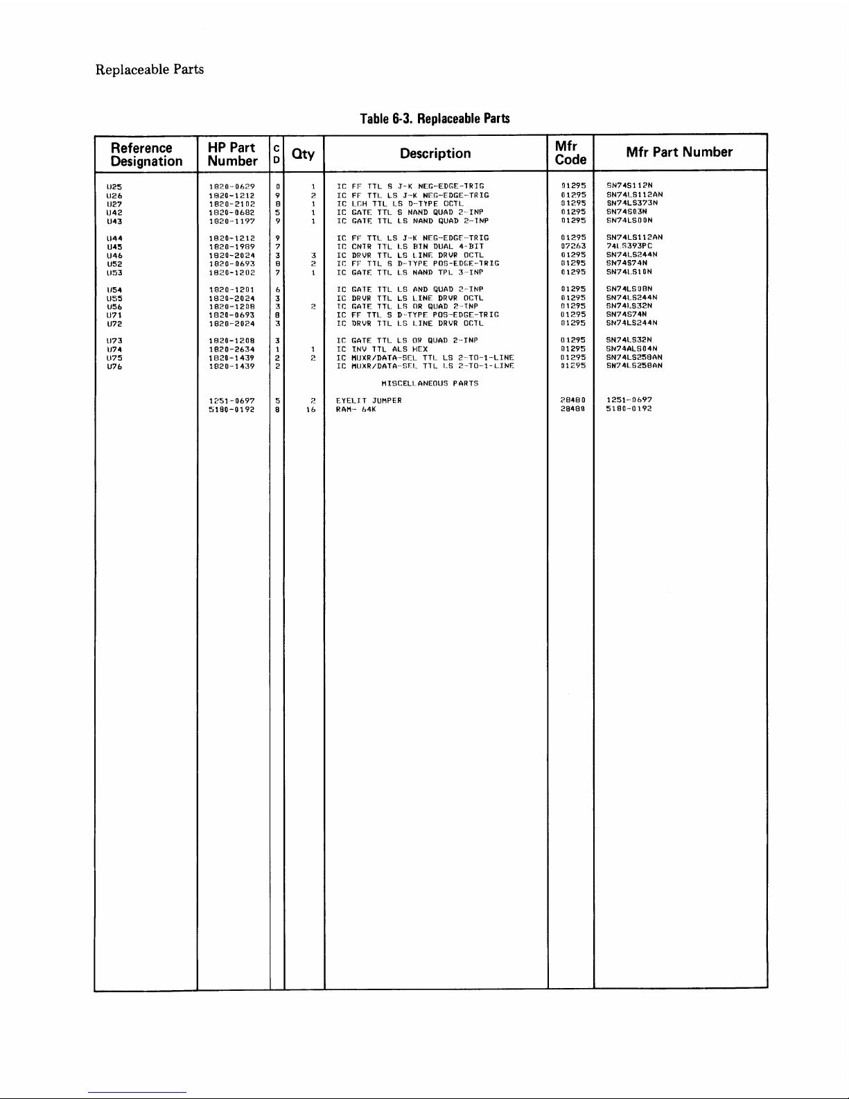
Table
6-3.
Replaceable
Parts
Description
IC
FF
TTL
S
J"K
NEG-"EDGE
..
·TR
IG
Ie
FF
TTL
LS
J'-K
NFG-FDGE-"TR
IG
Ie
LCH
TTL
LS
D-·TYPE DCll..
Ie
GATE
TTL 8 NAND
QUAD
2
..
INP
IC
GAlE
TTL
l..8
NAND
QUAD
2--tNP
Ie
FF
TTL
L8
J"-K
NFG"-EDGF"-TRIG
tC
CNTR
TTl..
L8
BIN
DUAL
4-InT
IC
DRVR
TTL
LS
l.INE
DRVR
oeTL
IC
FF
TTL
S
D-
..
TYPE
POS-·EDGE-·'
RIG
IC
GATE
TTL
l.S
NAND
TPL
31NP
IC
GATE
TTl
..
l..S
AND
QUAD
2
..
·INP
IC
DRVR
TTL
l..S
LINE
DRVR
OCll..
TC
GATE
TTl..
L8
OR
QUAD
2
..
1NP
Ie
FF
TTl
...
8
D·-TYPE
P OS"-['OGE'-
TR
I G
IC
DRVR
TTL
LS
I..INE
DRVR
OCTl_
Ie
GATE
TTL
L8
or~
QUAD
2
..
-JNP
IC
INV
TTl..
AL8
HEX
IC
HlJXR
IDATA·-SEL
TTL
LS
2
..
TO-1-'LINE
IC
MUXR/DATA
..
·SFI..
TTl..
1..8
2"T()--1-1.1NE
MH1CEU.ANEOl.IS PARTS
EYEI..JT JUMPER
RAM·- 64K
Mfr
Code
n1295
01;"95
01295
01295
01295
01295
07263
01295
01295
01295
01295
01295
01295
01295
01295
01295
01295
01295
31295
,'8480
28480
Mfr
Part Number
HN74S11?N
SN74L5112AN
5N7·4L5373N
SN74S03N
SN74LSOllN
SN74L5112AN
741
..
S393PC
8N74LS244N
SN74574N
SN'74LS10N
SN74L808N
8N74L.5244N
SN741..832N
8N74S74N
8N74L5244N
SN'74L532N
SN74AL804N
SN'74LS258AN
SN741.S258AN
1251-,0697
5190,-0192
Page 23

M A N U F
ACT
U R E R S
COD E LIS
T
AS
OF
08/05/82
HFR
ZIP
NO.
MANUFACTURER
NAME
ADDRESS
CODE
00000
ANY
SATISFACTORY
SUPPLIER
01121
ALLEN-BRADLEY
CO
MILWAUKEE
WI
53204
01295
TEXAS
INSTR
INC
SEMICOND
CMPNT
DIV
DALLAS
TX
15222
01961
PULSE
E,NGINEE1IING
INC
SAN
DIEGO
CA
92111
04'713
MOTOROLA
SEMICONDUCTOR
PRODUCTS
PHOENIX
AZ
85008
07263
FAIRCHILD
SEMICONDUCTOR
DIV
MOUNTAIN
VIEW
CA
94042
16299
CORNING
GLASS
WKS
COMPONENT
DIV
RALEIGH
NC
2'7604
19701
MEPCO/ELECTRA
CORP
MINERAL
WELLS
TX
'7606'7
24546
CORNING
GLASS
WORKS
(BRADFORD)
BRADFORD
PA
16'701
28480
HEWLETT-PACKARD
CO
CORPORATE
HQ
PALO
ALTO
CA
94304
34344
MOTOROLA
INC
FRANKl.IN
PARK
IL
60131
343'71
HARRIS
SEMICON
DIV
HARRIS-INTERTYPE
MELBOURNE
FL
32901
34649
INTEL
CORP
MOUNTAIN
VIEW
CA
95051
50088
MOSTEK
CORP
CARROLLTON
TX
'75006
555'76
SYNERTEK
SANTA
CI.ARA
CA
95051
56289
SPRAGUE
ELECTRIC
CO
NORTH
ADAMS
MA
0124'7
9163'7
DALE
El.ECTRONICS
INC
COLUMBUS
NE
68601
 Loading...