

Page 1
P
f'
()
c:
~?~:;~:;
()
T'
Mod u 1 e
Manual
DATA
Part
TERMINAL
TECHNICAL
No.
13220-91087
REVISED
JAN···
()
4····B2
INFORMATION
Printed
in
HEWLETT~PACKARD
U.S.A.
Page 2
P
f'
0 c
(~~:;
~:;
0 7' M
()
d u 1 e
Manual
The
inforMation
w:i.ti"lou"t
HEWl..ETT····Pt-.CI{ARD t'\AI{EB
MATERIAL,
notic€~.
INCLUDING,
MERCHANTABILITY
shall
con~)f:~quf.·!n·t:i.al
or
use
not
of
be
this
contained
AND FITNESS
liable
dat
for
...
aqE~s
Material.
NO
BUT
in
Part
No.
13220-91087
I~EVISED
JAN···
()
4····0t?
NOTICE
in
this
WARI~ANTY
NOT
dOCUMent
OF ANY
LIMITED
FOR A PARTICULAR
errors
c()nn~:~ction
contained
with
TO
is
I{IND
THE
IMPLIED
PURPOSE.
herein
th(·!
fUl'nis;hinq,
subject
WITH
or
to
change
'~EGAI~l)
TO
WARRANTIES
Hewlett-Packard
for
incidental
~)E~l'for'Manc:~?,
THIS
OF
or
This
cop
dOCUMent
Y
7'
:i.
q h
photocopied
Pac k (;.
r'
d C
NOTE:
t.
All
or
()
i'\
pan
Thi~:;
~:)
0!
r'
contains
r' i
<;.I
reproduced
y .
Cop
yr'
iqh
docuME!nt
:i.
f:·!
s T
f..!
h t
~:;
t c
C h n i
proprietary
i:\ "
f..~
r'
f:'~
~:)
f:! r' v
without
j.9S;:-!.
is
cal
par't
I n
for'
by
inforMation
E!
d . N
the
HEWI...ETT--PACKARD COMPANY
of
Mat
()
prior
th(~
~?'6;:~XX
ion
P i:\
P a " t 0 f t h
c:
k a
which
written
DATA
(J
f!
(H P j. 3
is
:i.
~:;
consent
TERMINAl...
;:~
protected
cI
0 c
lJ
M
;:?
()
) .
~;!
n t
JII\
a y b
of
Hewlett-
pr'oduct
by
f:!
Page 3
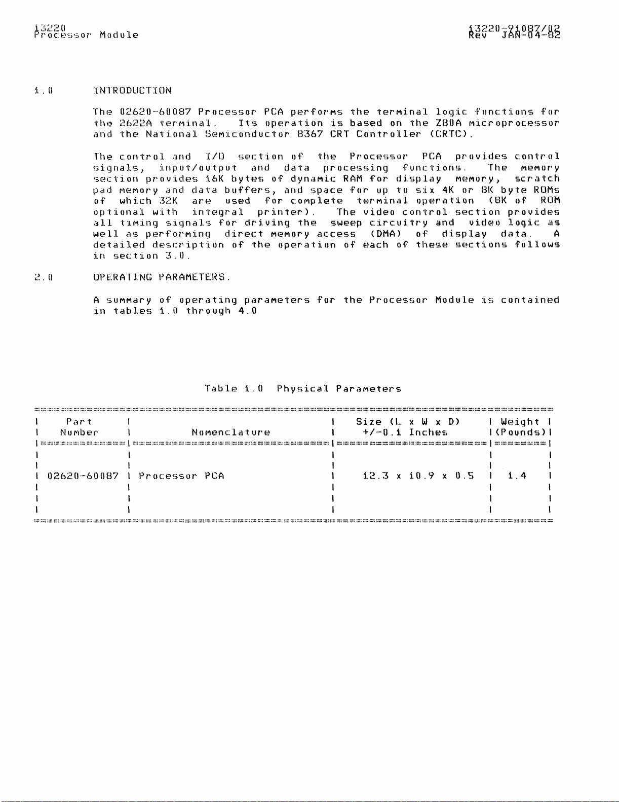
i.O
IN"l"RODUCTION
The
02620-60087
the
2622A
and
the
The
control
~;>
i q n a 1
section
pad
MeMory
of
which
optional
all
tiMing
well
detailed
:i.
n
~:;ec
as
terMinal.
National
~:>
,
:i.
n
provides
and
32K
with
signals
perforMing
description
t
ion
3.
and
put
0 .
Processor
Its
SeMiconductor
I/O
/ 0 u t
16K
data
are
integral
section
put
bytes
buffers,
used
for
driving
direct
of
PCA
operation
and
of
for
printer).
MeMory
the
operation
perforMs
8367
of
the
d
i~
tap
dynaMic
and
space
COMplete
the
access
the
is
based
CRT
Controller
Processor
roc
(~s~:;:i.
RAM
for
for
terMinal
The
video
sweep
of
circuitry
each
terMinal
on
n(J
display
up
to
CDMA)
of
the
(CRTC).
PCA
fun
c t j. 0
six
operation
control
of
these
logic
Z80A
provides
n~:;
MeMory,
4K
section
and
display
sections
functions
Microprocessor
control
.
or
video
The
8K
(8K
MeM
scratch
byte
of
provides
logic
data.
follows
for
0 r' y
RUMs
ROM
as
A
2.0
OPERATING
A
SUMMary
in
tables
PARAMETERS.
of
operating
1.0
through
Table
paraMeters
4.0
1.0
Physical
for
the
ParaMeters
Processor
Module
is
contained
===============================================================================
Par'
1
t S i z e (I... x W x
NUI"',IHH'
1
NOMf:·~nclatul'~~
1
+/
....
0.1
Inche~;
D)
1
W(~
i q h t 1
1
(Pounds>
1
1=============1==============================1=======================1========1
1 I 1 1 1
1 1 1 1 1
1
02620-60087
1
Processor
PCA
1
12.3
x
10.9
x
O.S
1
1 1 1
1.4
1
1
I 1 1 1
1 1 1 1
===============================================================================
Page 4
1
:'5;:~:~O
Pl'
()Cf.~<':;~;()l'
Mod
u Ie'
1
~5220
....
f/1 0 H'7 / ()
Rev JAN-()4····f32
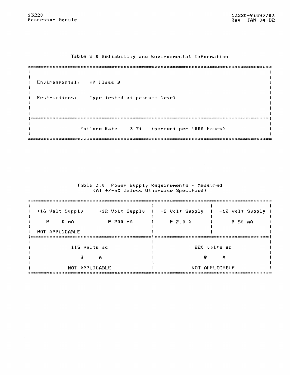
~5
Table
================:========~======================================================
I
I
I
EnvironMental:
I
I
I
Restrictions:
I
I
I
I==~===========~==============================================================
I
I
I
===================~======~====================================================
Failure
Table
2.0
HP
Class
Type
3.0
(At
Reliability
B
tested
Rate:
Power
+/-5%
Unless
at
product
3.71
Supply
and
EnvironMental
(percent
RequireMents
Otherwise
level
InforMation
per
1000
-
Specified)
hours)
Measured
===~=============================~=============================================
+16
Volt
ill 0
I
NOT
I
:::
::;:
I I I
I
I I I
I
I I I
I
APPLICABLE I I I I
:~:
::::
::::::::
::::
Supply
MA
::::::::::::
::::::::
::::
::::
115
NOT
+12
Volt
@
:;::
::::
::::::::
:'~:::::
:::: ::::
::::
::::
:.::::::
:::: :::: :::: :::: ::::
volts
~
APPL.ICABL.E I
ac
A I
200
Supply
MA
:::::-.::::::
::::
::::::::
::::
::: I =::::::::::::
I
+5
Volt
@
:::: ::::
::::::::
Supply
2.0
A I @
::::
::::::::
:.~:::::
::::::::::::
220
NOT
I
I
-12
Volt
I
I
:::: ::::
::::::::::::
:::::::::".::
:::::::::::
volts
@.
APPLICABLE I
ae
A I
Supply
SO
MA
:::: :::: = :::: = ::::
::::
::::::::
= I
I
===============================================================================
Page 5
13~~2
()
P
f'
0 C
£~
~:;
~:)
()
:1.
3~~~:~
0 ···9108'7/04
R
(::~
f'
M
()
d u 1 e
v JAN···
()
4···B;?
Table
===~==========~===~========~===================================================
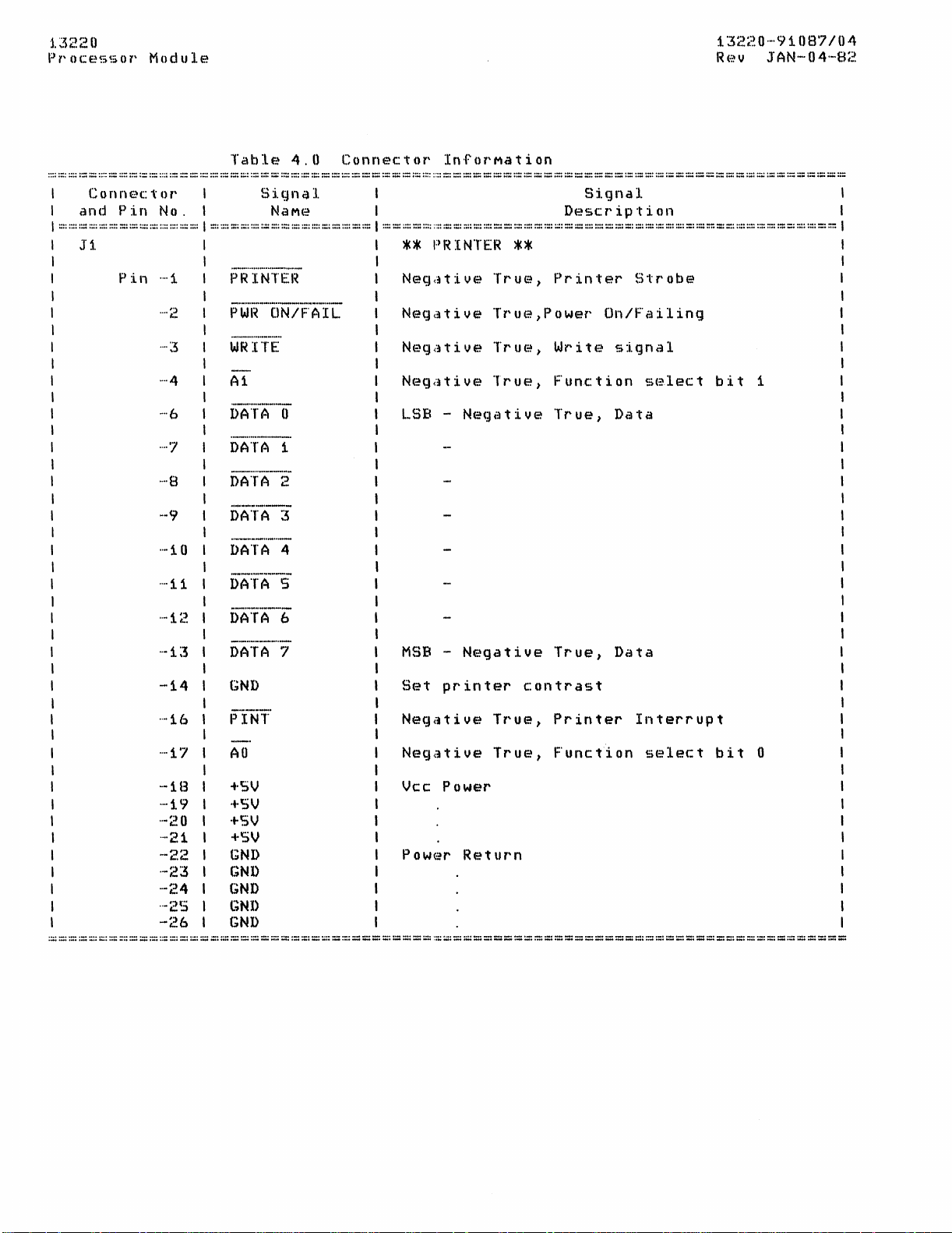
Connector
1
and P in
No. 1
1==============1================
J1
Pin
···1
....
2
....
~5
....
4
·
..
··7
....
8
·-9
....
:1.
0 I
....
:1.1
....
:1.
;,?
"-L3 t
1
1
I
PRINTER
I
1
PWI~
I
WRITE
1
1
1
Ai
1
DATA
\
1
DATA
\
\
I
DATA 2
t
1
DATA
I
DATA
I
I
DATA
I
t
DATA
I
DATA
4.0
Signal
NaM(~
ON/FAIL
()
1
:5
4
S
6
7
Connector
InforMation
Signal
Description
=============================================\
**
PRINTER
Negative
Negative
Negative
Negative
LSB -Negative
MSB -Negative
**
True,
True,Power
True,
True,
Printer
Write
Fun~tion
True,
True,
Strobe
On/Failing
signal
select
Data
Data
bit
1
I
I
-14
·
..
·16
....
1·7
-1t3
-·19
"-20
....
21
·-22
..
-;~3
-24
"-25
-26
GND
PINT
AO
+SV
+SV
+SV
+SV
GND
GND
GND
GNU
GND
Set
printer
Negative
Negative
Vcc
Power
Power
Retul'n
contrast
True,
True,
Printer
Function
Interrupt
select
bit
0
Page 6
1.
~5~~2()
Pl'OC(~SS)Ol'
Module
13220-91.08'7/0S
Rev
JAN-()4-B2
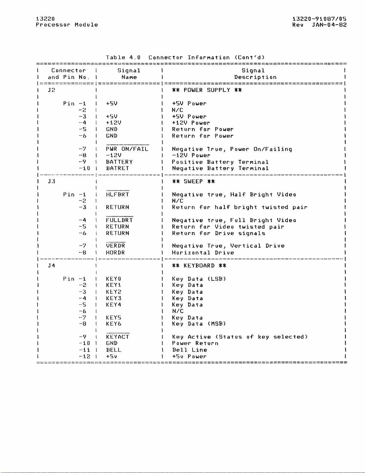
Table
===============================================================================~
I
Connector
I
and
Pin
No.
I
\==============1================
I
J;:.~
I 1
I
\
Pin
\
\
I
I
I
I
\
I
I
I
........................................ -............
I
J~3
I
I
I
\
\
I --4
\
Pin
\
I I
I
\
I
..... -........
, _
.......... -........ -...........
\
J4
\
I
I
I
I
\
I
I
)
Pin
I
-·1
-.~:~
-3
-4
-S
-6
-'7
-8
-9
-10
-1
-2
-3
-5
-6
....
'J
-8
....
1
....
2
·
..
·3
...
-4
·
..
·s
·
..
·6
....
·7
-·B
+5V
+SV
+12V
GND
GND
.. _ ...
_.
PWR
-1.2V
BATTERY
1
BATRET
'I
._.-
....
'''' .-..... -..................... -•• -.-.-
1 I
.....
__
HLFBRT
RETURN
........ _ ...........
FUL.L.BI~
RETURN
RETURN
iJ'f~:'ifi)rf
I
HORDR
-.
:1
.......... -............ -............... -............. -•.
\(EYO
KEYj
KEY2
KEY:~
I<EY4
KEYS
KEY6
Signal
NaMe
__
._
... _ ..
__
ON/FAIL
..
_.
__
....
__
. I
_._._.
.
4.0
.......... _ ......
T \
Connector
_.
-
InforMation
(Cont'd)
Signal
Description
==============================================
**
+SV
N/C
+5V
+1;':'~V
R€~t
Ret
Negative
-12V
Positive
I
Negative
I
..
-.--.-...... -.-
**
I
Negative
I
N/C
I
Return
I
Negative
I
Return
\
Return
I
Negative
I
Horizontal
**
Key
KE~y
Key
Key
Key
N/C
K(~~y
)(ey
POWER
Power
Power
ur'n f
urn
SWEEP
KEYBOARD
Data
Data
Data
Data
Data
Dc:l
Data
SUPPL.Y
Power
01'
for'
True,
Power
Battery
Battery
....... -.............
_.-.-
**
true,
for
true,
for
for
True,
(LSB)
ta
(MSS)
**
Power
P
ow(~r
Power
........... , ..... -..........
Half
half
bright
Full
Video
Drive
Vertical
Drive
**
On/Failing
TerMinal
TerMinal
-.-.-
.. -....
Bright
twisted
Bright
twisted
signals
'''' .-...
_.-
Video
Video
pair
Drive
.... _ .... -..... -.....
pair
_._.-
- -' -
..
_.-
I
·
..
·9
.... 1 ()
····1.1
....
12
================================~===============================================
KEYACT
GNI>
BELL..
+Sv
Key
Active
Pow(~r
Bell
+5v
Line
Power
Return
(Status
of
key
selected)
Page 7
j.
~5;.:!.2
0
Pr'oc(::~ssor'
Module
1
~5220'-91
Rev
08'7/06
JAN-()4'-B2
Table
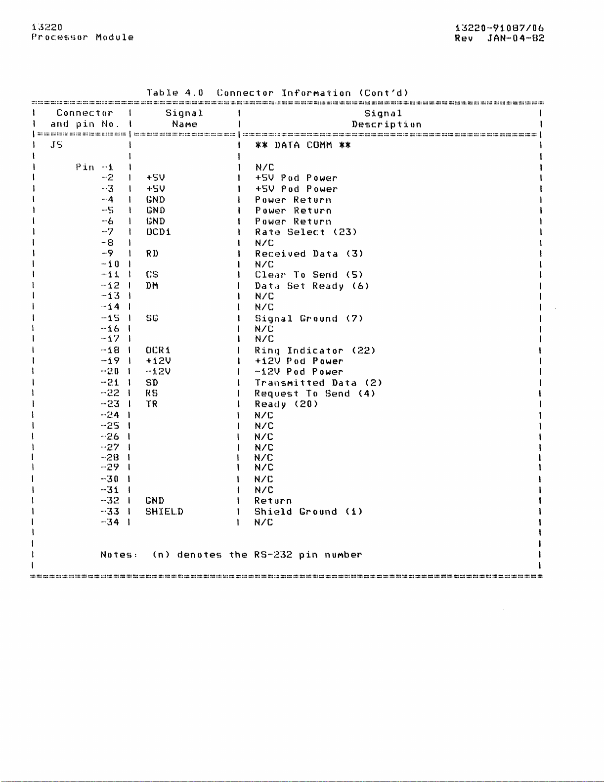
~===============================================================================
Connector
and
pin
No. I
4.0
Signal
NaM€~
Connector
I
InforMation
(Cont'd)
Signal
Des;cr'iption
==============1================1==============================================
JS
Pin
....
j.
-.;~
"'~3
....
4
~~S
"~6
..
~'J
..
··8
..
~9
..
··10
·
..
·1 i
....
12
"~13
·
..
·14
....
1 S
-··16
....
j.
'J
....
18
·
..
·j.9
....
;?
0
--21
.. -;;!;,?
....
;:?~~
"-;?4
"-25
....
26
-~27
..
··;,?8
..
-29
-~3
()
"-31
"-3;.~
..
··33
....
~34
+SV
+SV
GN!)
GNl>
GND
DeDi
RD
(,(:'
.,,,:>
DM
SG
OCR1
+1;~V
--1;:!V
SD
RS
TR
GND
SHIEL.l)
DATA
COMM
**
N/C
+SV
Pod P
+SV
Pod
P()w(~r
P
OWf-~r'
P()w(~r
Rat(:~
Nit
R
(~c
f:d.
Nit
Clf~dr'
Di:l
ta
N/C
Nit
Si~}na
NIt
N/C
Rinq
+12V
'-1~~\)
Tr';HlSMl.
r~eqllest
Ready
Nit
N/C
NIt
N/C
N/C
N/C
Nit
N/C
Return
Shi(-.~ld
N/C
ow€~r
Power
R(~tul'n
I~et
urn
Return
S~~lect
l)clti:\
V
(·~d
To
Send
S(?t
Rei:ld
Gr' 0 und
1
Ind:i.cator
Pod
Power
Pod
Power
t
t(~d
To
(20)
Ground
**
(23)
y
Data
Send
(3)
(5)
(6)
(7)
(~~2
(4)
( 1 )
)
(2)
(n)
denotes
the
RS-232
pin
nUMber
================================================================================
Page 8

1
~3~!'~~0
Pl'
()c€-~~:;s()r'
M()d u le
1:3220·-91.
Rev
JAN····
OB'7
0 4'-(32
10'7
3.0
FUNCTIONAL
Refer
tiMing
parts
the
and
CONTROL.
t()
diagraMs
list
()peration
lID,
AND
Clock
A
25.7715
video
74LS244
then
is
clock
4.4V.
which
d()t
(US11)
divided
shaped
for
This
the
lOOA
The
laOA
tion
signals
It
which,
branch
bus
b u
functions
also
request
~:)es
.
to
responds
when
to
DESCRIPTION
bl()ck
diagraM
(figs.
(fig.
MeMory,
I/O
MHz
10)
of
the
and
SECTION
crystal
frequency.
to
beCOMe
by
seven
by
Q4
and
the
ZaOA,
clock
datacoMM
Microprocessor
of
the
read
and
to
enabled,
its
interrupt
signal,
located
three
video
is
This
by
its
associated
which
is
also
chip
processor
write
two
externally
interrupt
service
NBUSREQ,
(fig.
4-8),
Major
c()ntrol.
attached
DRCX,
the
748163
has
divided
(U613)
perforMS
data
1),
scheMatic
COMponent
in
the
appendix.
sections
to
is
buffered
buffered
(Ub11)
circuitry
a
zero
by
uses
to
the
peA.
frOM
generated
current
routine.
allowing
location
of
the
by
dot
level
two
to
produce
Major
It
provides
and
to
execution
the
diagraMs
the
CRTC
the
rate
to
produce
to
<
produce
baud
control
both
interrupts,
The
CRTC
diagraM
The
following
Processor
which
CRTC
clock.
produce
0.4SV
a
rates.
and
addresses
MeMory
and
ZBOA
also
control
(figs.
(fig.
peA)
oscillates
and
again
This
3.6816
MHz,
a
SYMMetrical
and a one
1.8408
data
and
and
I/O
NNMI
cause
the
responds
of
the
2,3),
9)
and
describes
control
at
the
by
clock
which
level>
MHz
clock
Manipula-
control
ports.
and
NINT,
ZaOA
to
systeM
a
is
to
a
At
power
prograM
initializes
non-volatile
an
error
indicate
enters
a
por'ts.
Three
frOM
MeMory
abled
74LS244's
the
into
during
instructi()n
in
an
instruction
signal
was
respond
frOM
full
be
the
latch
th~:~
address
speed.
used
ZaOA
U610
ZBOA.,
up
MeMory
variables
is
detected
the
Major
Z80A.
six
fetch
used
within
by
installing
to
wait
and
(or
reset)
beginning
at
and
MeM()ry
failing
10()P
(CMOS)
a
series
ROM
responding
(U4'7,U57,U511)
The 1 of a decoder,
blocks,
a MeMory
by
read
the
each
NMl
fetch
to
provide
the
required
or
300
ns
frOM
[PROMs
or
ROMs
JUMper
one
cycle
ass()ciated
the
ZaOA
address
devices
and
of
or
RAM.
BK
by
the
signal.
is
less
an
early
tiMe.
enable
with
l()nger
gating
begins
OOOOH.
according
perforMS
beeps
After
to
inputs
buffer
bytes
TNRD
than
enable
are
450
WS
and
during
provides
executing
A
to
a
self
are
issued
inintialization
frOM
the
U76,
long.
and
that
ROMs
ns
reMoving
is
TNMREQ
Since
for
of
with
required
access
instructi()n
the
routine
inforMation
test
the
of
to
the
keyboard
address
used
The
to
addressed
signals
the
tiMe
a
MeM()ry
the
ROM
access
t()
run
tiMes
JUMper
fetches.
required
instructions
is
executed
contained
ROM
and
keyboard
the
and
and
control
separate
ROM
()r
to
read
read,
allowing
tiMes
the
frOM
W6,
address
which
wait
frOM
which
RAM.
which
prograM
datacoMM
lines
prograM
is
en-
during
the
data
the
it
of
350
systeM
causes
The
quad
signal
in
If
an
NM1
to
ns
at
May
to
Page 9

13220
Processor
3.1.3
Module
I/O
Ports
CMUS
The
Z80A
I/O
addresses
accuMulator
used
to
configuration
respond
each
S
volts
Q3,
before
beCOMe
CMOS
May
be
standard
CMOS
within
tiMe
is
Makes
the
defined
contents.
replaced
read/COMpleMent/write
error
DATACOMM
is
capable
contents
access
data
the
CMOS
always
sure
l80A
since
froM
the
that
buses
at
If
by
the
of
the
appear
locations
is
stored.
I/O
cycle
RAM
is
on
t~e
during
power
power
an
HM7611
prOM
addressing
ZaOA
on
in
accessed.
CMOS
a
beCOMe
on.
on
configuration
PROM
cannot
2S6
appear
bits
the
Since
on
A8-A1S.
nonvolatile
the
tiMe a wait
Diodes
supply
power
pin.
off
undefined
During
(however
test
be
for
written).
different
address
CMOS
state
the
and
power
is
it
the
CMOS
bits
I/O
addresses
CMOS
RAM
is
is
generated
CR6-CR8
EMMitter
CMOS
is
reMains
off
the
to
be
fixed,
Must
be
self
13220-91087/08
Rev
input/output
AO-A7
RAM,
not
ensure
U73,
fast
that
follower
always
so
until
battery
the
realized
test
would
JAN-04-82
ports.
and
0-7FH
the
are
where
enough
(by
to
U6l0)
around
Circuit,
disabled
buses
Maintains
COMS
that
RAM
the
show
a
The
parallel
functions
laOA
selecting
unique
the
decoder.
The
therefore
status
USi4,
levels
(SD),
driver
(DM),
The
to-point
SY6SS1
to
required
as
four
the
tiMing
rising
The
status
are
signals
and
receiver,
(+-12V)
terMinal
1 (OCD1).
optional
datacoMM
environMent.
siMultaneously
tiMe
each
110
and
by
intervals
character
baud).
the
the
SY65S1.
detection
selectable
and
detected
overrun)
is
read
reception
to
when a
rates
SY6SS1.
Asynchronous
serial
conversion,
for
read
only
read/write
of
the
edge
of
addresses
inputs
forced
are
routed
U614,
and
ready
Received
control
subsysteM
(full-duplex)
(asynchronous).
is
fraMed
The
addition
of
The
(in
the
datacoMM
by
the
SY6SS1
the
ZaOA
character
are
set
serial
and
function.
6500
SELDC
of
of
the
to
their
vice
(TR),
receiver
operates
Characters
by a
of
fraMing
parity
by
Means
by
COMMunications
four
error
data
write
detection
COMMunication.
only
This
series
which
the
SY6SSl
devices.
SY6SS1
is
(U613)
produce
active
through
are
versa.
signals
~sed
request
another
to
TranSMitted
are:
1
(OCR1),
in
an
convert
to
asynChronous,
May
with
start
the
bits
(for
character
To
bit
fraMing
for
error
achieve
configuration
which
reports
of a status
is
received.
the
ZaOA
in
Interface
ports
is
done
The
inverted
are
undesirable
low
states
port.
frOM
send
(RS)
receive
and
clea~
be
tranSMitted
flow
hardware
and a stop
bits
the
for
received
detection)
Menu)
errors
register
The
an
internal
Adapter
and
baud
It
with
to
SY6551
frOM
AO-A7H.
while
RS-232
TTL
signals
and
d~ta
to
full-duplex,
occurring
bit
tranSMitted
characters
of
and
(parity,
in
data
reqister
perforMS
rate
generation
appears
address
COMpensate
is
selected
U24,
the
results
the
line
levels
are:
optional
(RD),
send
(eS).
and
over
synchronization
(2
stop
characters
the
character
is
also
fraMing,
the
SY6SS1
tranSMission
within
the
to
the
bit
TA2
for
the
1
of
and
necessary
driver,
to
RS-232
send
data
control
data
Mode
point-
received
randOM
bits
are
done
generated
and
which
and
the
by
8
at
is
Page 10
13220
Processor
Module
13220-91087/09
Rev
JAN-04-82
Rates
9600
The
lines
provide
are
selectable
baud.
datacoMM
to
connect
direct
power-on
terMinal
(esc
f)
is
the
disconnect
by
DM
which
displayed
host
to
when
halt
tranSMission
configuration).
strap
the
self
status
Upon
with
ModeM
test
lines
receipt
interrupt
the
datacoMM
clearing
character
for
delete
which
character
the
ready.
the
on
the
active
its
rate
to
detect
are
signal
interrupt
the
and
errors
status
the
hardware
TR
and
TR
line
ModeM.
causes
bOttoM
allows
The
default
for
active
of
(NINT)
interrupt,
places
to
(in
inputs
terMinal
Upon
is
the
(the
state
state
dual
the
a
character
it
(parity,
be
placed
the
datacoMM
and
outputs
to a host
handshaking
RS
lines
receipt
brought
The
presence
indicator
center
the
of
terMinal
terMinal
of
OCDl
being
speed
ModeMS. OCRl
presence
high
(+12V).
frOM
to
the
lBOA.
service
routine
and
into
the
fraMing
in
configuration
provide
COMputer
between
are
activated
of a ModeM
inactive
of a ModeM
"LED"
the
display.
to
tranSMit
May
ignore
is
controlled
low
of
the
(inactive).
loopback
datacoMM
This
which
if
no
errors
datacoMM
or
the
buffer.
the
disconnect
for
(an
causes
reads
buffer
overrun)
Menu) frOM
the
via
terMinal
to
indicate
.about
connection
asterisk
The
CS
data
CS
depending
by a configuration
is
Monitored
test
the
SY6SS1
the
the
are
present,
in
are
necessary
a ModeM,
and
escape
two
seconds
is
'*')
signal
and
goes
on
This
line
in
hood.
generates
ZaOA
to
SY6S51
RAM.
present
110
control
or
host.
that
the
sequence
detected
to
frOM
the
inactive
datacoMM
selects
datacoMM
All
ModeM
branch
status,
inputs
th~
Characters
cause
to
to
At
to
be
an
to
a
Teus
The
PORTS
reMaining
biderectional
loading.
enabled
U25
port
by
th~
(colUMn
More
(scan
for
forMS
returns
keyboard/display
address)
frOM
line
keystatus
they
for
range
are
each
of
I/O
bus
The
signal
all
the
keystatus
the
the
eRTC
count)
shift
later
of
read.
the
keyboard
ports
driver,
I/O
accesses
status
are
scan
frOM
register
first
addresses.
are
TNRD
port
of 8 keys
port
supplied
line
the
(a
The
colUMn
sixteen
buffered
U37.
selects
except
by U26
outputs
CRTC
high
display
This
the
located
at
(U26).
change,
bit
address
to
was
direction
CMOS
RAM
at
a
tiMe,
Four
(located
(row
keystates
indicating
is
rows
the
ZaOA
done
and
address
which
bits
at
address).
key
increMented
thereby
data
because
of
the
driver
datacOMM.
80H.
keys
of
the
address
As
the
are
clocked
active)
(during
scanning
bus
of
The
are
key
B8H)
row
by
the
data
bus
which
keystatus
deterMined
address
and
three
address
into
frOM
the
which
an NMI)
the
entire
is
Page 11
j.~3;~~?O
P
l'
()
C
~~ s ~:;
()
f'
r1
0
cI
u 1 e
The
keyboard/display
horizontal
the
n
~:;
hap
the
I«~~
y
enabled
blinking
sync
(~d
b Y
boa
l'
d / d i
and
latches
characters.
pulses
(~4
a n
~;
P
:I.
e) y
port
down
cI
i
the
also
t~:;
a
POl"
t d
signal
enables
to a bell
,;)
soc i ate
E-~
t (;H' Min
frequency.
d
c:
E~
which
a
counter
i
l'
cui
w h e t h
deterMines
t . T
£o~
r
£om
(U114)
The
I'\(~
reM a i n i n g
han
c
£o~
the
L3220-91
Rev
which
bell
Men
t
<.!;
blinkrate
OB'7
JAN-'O
counts
signal
bit
will
/10
4···82
is
S 0 f
b e
of
The
NNMI
externally
select
the
address
clears
latch
The
l'
(.:~
a d t h
with
the
f.·H\i:\bling NMI.
systeM
E~ V (~H'
the
signals
The
integral
the
printer
NPRINTER
the
printer
perforMing
TA1
and
status
is
enabled
printer
data
the
Ji
Each
pair
bit
pullup
pin
character
of
11
character
byte
bits
for
to
in
of
the
fifteen
character
the
data
dots
for
COMMand
expanded
(non-Maskable
by
a D
NENNMI
bit
TAO
latch,
status
tic
hardware.
discussed
printer
bus,
signal
via
a
write
data
for
is
lines
read
read
detected
back
TU1.
resistor
is
pulled
bytes
if
the
the
pair
the
following
saMe
horizontal
horizontal
font
in
and
printing.
to
print
and
cOMpressed
flip-flop
signal
is
the
disabling
port,
alb
1
elf)
It
above
the
is
active.
U16
and
operation
TDO-TD7
frOM
operations
by
TU1
will
R1.
low
in
the
being
character
indicates
a
1S
translates
the
character.
interrupt)
(half
of
the
data
input.
NMI,
U36,
located
k s i 9 n a 1 (
also
port
and
data
provides
also
at
address
being
The
half
of
to
selecting
the
printer
frOM
reading
be
low
When
by
printer
Made
the
the
printer
is
up
cell
the
byte
indicate
scan.
scans
by
1S
cell
the
horizontal
Each
30
bytes
Modes.
of
port
decoder,
This
while
VB
l.
A N
the
Monitors
latched
processor
U1S.
the
printer
the
on
the
printer
status
if
the
printer
forMed
of
the
is
state
the
Thus
of
fifteen
the
May
of
The
signal
U612).
Means
a
at
address
K)
f 0
inputs
the
98H
buffers
writes
Printer
particular
the
frOM
printer
is
therby
by
dot
scanned
of
every
state
character.
be
created.
dot
dot
data
printer
to
Port
clocking
that
write
f'
S Y n
c:
f~r
integral
in
control
with
upper
port.
the
is
connected
indicating
30
bytes
data
horizontally.
of
pairs
inforMation
are
is
also
the
addresses
a
to
90H
allows
h
l'
0 n i z i n g
the
data
the
data
address
function.
half
The
printer
not
of
needed
other
the
of.bytes
In
The
followed
ZaOA
the
latch
write
port
to
89H
the
the s of
datacoMM
printer
continuously
printer
and
is
specified
COMMands
lines
of
U1S
presence
and
connected
to
the
connection.
dot
data,
to
dot
while
interstitial
this
printer
into
able
to
is
Masked
B8H
to
8FH
while
port
sets
88H
the
ZaOA
twa
status
s~atus.
when
TAO
the
and
Printer
which
of
the
checking
due
processor
each
forM
The
the
first
seven
dots
correspond
way
any
buffers
vertical
by a print
print
to
l'
to
to
by
is
to
in
e
The
reMaining
video
inverted
section
to
TBUS
and
provide
one
the
port
for
clock
located
the
at
datacoMM
for
the
ASH
section.
latch
latches
(U3S).
SOMe
The
signals
NMODEM
to
signal
the
is
Page 12
13;:~~~
0
Pr'ocf.~~:;~:;or
Module
13~?20·M·91
R
(~v
J
AN
OB7 /1.1
.. -()
4·-S;:!.
3.2
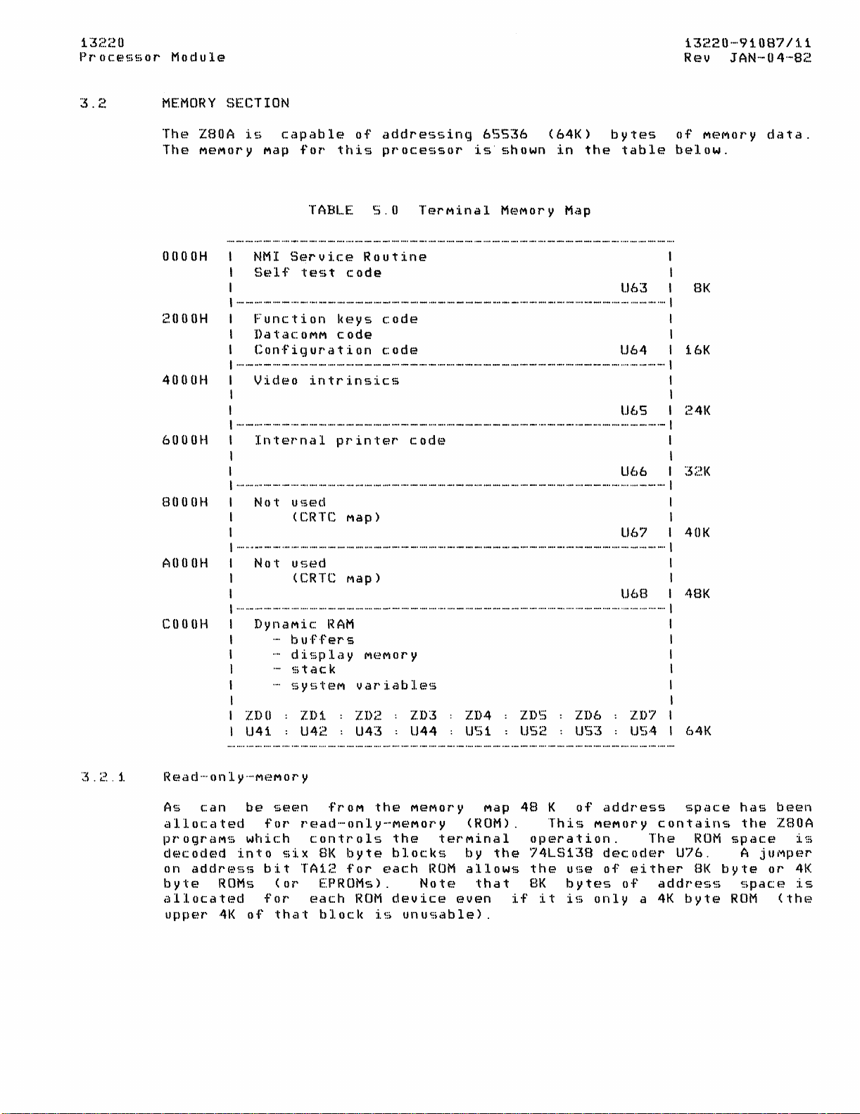
MEMORY
The
Z80A
The
MeMory
OOOOH
2000H
4000H
6000H
BOOOH
AOOOH
CO
()
OH
SECTION
is
capable
Map
NMI
Service
S~~lf
for
TABLE
t€~st
of
this
code
addressing
processor
S.O
Routine
is'shown
TerMinal
65536
MeMory
(64K)
in
Map
the
bytes
table
U63
Function
l)at
..
:lCOMM
Configuration
Video
I
Internal
I
I
I
................
_. -..................... M ..................... _ ..................... _ ..............
I
Not
u~:;ed
I (CRTC Map)
I
I
.........................................
I
Not
us(~d
I (CRTC Map) I
I
I
........................................
I DynaMic
I
I
I I
I I
I
-
buffers
-
display
stack
-
systeM
ZDO
: ZDt : ZD2 : ZD3 :
I U41 : U42 : U43 : U44 :
keys
code
intrinsics
printer
-
............................
_.
'M'
'M'"''
........
I~AM
MeMory I
variables
code
code
U6S
code
M'
........ M ...... _ .....................
""
............................ _ .............. -................................. _ ..
U66
_.
_. M ... M .........
M.
.... .... ....
U67
....
_. _ ...
........
U68
-' -......................... -.................... _ .............................................................. _ ..
ZD4 : IDS
US1
: US2 : US3 : US4 I 64K
: ID6 :
ID7
M.
of
MeMory
below.
HK
16K
~~41<
~5:r:.!\(
I 40K
I
I
I
4BK
I
I
I
I
I
I
data.
~3.
2.1
R€~a
d·
..
· on 1 y
As
can
allocated
prograMS
decoded
on
address
byte
ROMs
allocated
upper
41<
··
..
M(-:~Mor
be
seen
for
which
into
six
bit
(or
for
of
that
y
frOM
the
MeMory
read-onlY-MeMory
controls
81<
TA12
EPROMs).
each
block
byte
for
ROM
is
the
blocks
each
Note
device
unusable).
(ROM).
terMinal
by
ROM
allows
even
Map
the
that
4B
K
This
operation.
74LS138
the
BK
if
it
of
MeMory
use
bytes
is
only
address
The
decoder
of
either
of
a
space
contains
ROM
has
the
space
U76. A JUMper
BI<
byte
address
4K
byte
space
ROM
been
ZaOA
or
(the
is
41<
is
Page 13
l
:·~;.:?;:!.o
P
l'
0 C
E~
S
\;)
0
l'
Mod
u 1 e
i
:~220-9i
R
~~
v J
AN·M.
OB'1
04···82
Ii,!
During
to
is
opcode
ns
clock
During
G~nabling
n
~:)
even
thE'
an
indicate
used
to
fetch
froM
address
cycle
a MeMory
fro
M i:l d d
when
Z80t-1
instruction
that
provide
therby
shorter
th(~
addl'f.~Ssf:~d
l'
(0
S
s)
using
dati-'l
but:;
an
or
read
the
450
without
RandoM-acceSS-MeMory
The
RAM
subsysteM
16K
x 1
bit
150
ns
and
bits
Th(~
Wf':i.
during
TDO-TD7
I~AM~;;
te
clC:ce5se~)
a
discussed
ZUOA
A Z80A
address
TNMREQ
shifted
(TNRFSH
O's
low
I~EAD/WI~
access
location
going
through
is
are
shifted
in
turn.
strobes
address)
circuitry
100
ns
frOM
TNMREQ
signal
COMpleting
dynaMic
MiniMUM
respectively
ar'e
acce~)~;(~d
DMA
below.
ITE
high)
in
row
NCAS-strobes
to
access
NCAS.
the
has
by
(direct-MeMory-access)
Refer
to
RAM
between
low
the
the
the
through
This
address)
goes
RAM
(opcode)
instruction
an
early
allowing
300
ns
than
frOM
ROM.
r e
of
0
r'
e n
ns
EPRUMs.
been
RAMs.
cycle
in
the
to
is
initiated
COOOH
output
shift
output
the
produces
in
the
addressed
When
high
and
cycle.
fetch
fetch
enable
the
froM
enable
a MeMory
ROM
the
Data
()
wa
its
buP·fering.
designed
The
MK4116-2
tiMe
thl'(;:O(-?
to
of
provide
ways:
lBOA d
figure
and
of
register)
of
U77
shift
the
MUX-changes
colUMn
the
1'5
Z80A
are
of
use
read
TNMREQ
is
t
Note
around
320
U1'
ing
6.0
by
FFFFH
U77
goes
register
RAM
address
cell.
shifted
the
Z80A
cycle
the
of
(note
ROM
ROMs
is
being
with
that
operation)
and
r'f.~quired
,1
t e s a r
that
(-?
data
r
the
has a MiniMUM
ns.
the
U41-44
16K
bytes
by
the
a
l'efl'€-~sh
cycle.
for
RAM
tiMing.
lowering
(RAM
would
U510,
low
be
by
also.
address
high
DRCX.
causing
tiMing
RAM
sequence
address
and
Data
is
finish~d
ouput
through
activates
in
process.
addressed
an
access
an
opcode
without
TNRD
valid
(~q
signals
app('OXiMatf.~ly
u
ire d for M (-?
is
placed
MK4ll6-2
and
US1-S4
of
RAM
ZaOA
Each
the
for
c yc
Ie
TNMREQ
of
range).
causing
As
As
the
outputs
as
inputs
activates
on
accessing
the
the
NM1
This
tiMe
fetch
wait
til 0 r y
directly
(or
equivalent)
access
supply
data
M~?MOr'y
and
by
the
signal
l's
TNMREQ
clock
QA-QD
follows:
to
internal
MDO-MD7
the
shift
signal
signal
during
on
is
states.
go
active
rea
tiMe
storage.
read
the
three
at
Prior
to
goes
occurs,
to
NRAS-
colUMn
is
vaild
RAM
register
an
350
o~e
470
d s
on
of
data
or
CI~TC
is
an
to
be
low
go
RAM
the
If
the
along
the
with
output
operation.
transparent
inputs)
outputs
For
a
write
data
goes
The
on
low
TNRD
Z80A
TNMREQ
of
placing
are
the
strobing
signal
is
perforMing
U77
When
latch
enabled
operation,
data
bus.
will
(TNWR
to
enable
the
NMUX
beCOMes
the
RAM
until
ApproxiMately
the
data
be
high
d
read
reMains
the
transparent
signal
transparent)
outputs
TNRD
the
and
ZaOA
into
disabling
operation
high).
goes
on
TNMREQ
lowers
the
that
the
one
Z80A
internal
the
the
The
TNRD
latch,
high
is,
ZBOA
go
high
TNMREQ
clock
transparent
TNRD
(as
the
data
again.
and
data
line
signal
U62)
MUX
outputs
bus.
places
later
latch
is
during
goes
the
in
latch
is
gated
the
low)
follow
The
the
TNWR
the
so
lowered
with
read
the
the
latch
output
line
RAM.
RAM
Page 14
13220
Processor
Module
13220-91087/13
Rev
JAN-04-82
outputs
a
read
register
zaOA
The
every
The
perforM
The
following
decoded
TA7
RAS-MUX-CAS
signals
unaltered
byte
eRTC
Twice
0),
perforM
inforMation
the
and
will
and
(active
and
for
the
latch,
USiO.
onto
recirculate
addressing).
will
operation
to
REFRESH
nature
two
l8UA
dynaMic
ZaOA
while
current
activating
buffered
control
DMA
DMA
Maintains
and
reMain
does
DMA
per
the
NBUSREQ
DMA
reMain
low,
action.
address
U62,
TNBUSAK
the
bus
never
with
cOMplete
of
dynaMic
Milliseconds
has
a
built-in
RAM
each
executed
the
and
not
video
of
on
so
buffers
instruction
TNRFSH
sequence,
high
the
transparent
appear
row,
signal
enhanceMent
the
Machine
the
until
by
U79
buffered).
TBUSAK
on
as
well
enables
and
takes
Mode
be
on
TNMREQ
the
RAMs
to
refresh
a 7
eRTC).
NBUSAK
bit
the
and
refreshing
during
on
the
on
cycle
NBUSREQ
to
provide
U47,
the
bus
as
the
the
(see
the
l80A
going
cycle.
requires
guarantee
refresh
without
MeMory
fetch.
refresh
INMREQ
the
refresh
latch
bus.
scan
to
These
enables
enable
lines
the
and
character
The
by
tristating
line
section
signalling
is
signals
US?
and
and
upper
recirculating
data
high,
the
function
requiring
refresh
counter
signals
that
is
6
ZaOA
ZaOA
raised.
both
US11
the
enables
the
load
four
3.3
bus.
shifting
that
contents
While
is
are
row.
cycle,
not
and
is
activated
data
responds
its
The
IBUSAK
are
and
CRTC
the
signal
bits
line
for
The
each
to
extra
counter
the
output
brought
enabled
14
(if
address
that
NBUSAK
(active
used
enable
to
place
output
of
buffer,
More
provide
Since
the
starting
(see
to
the
to
to
the
cycle
1'5
row
of
which
instruction
on
MeMory
so
to
section
NBUSREQ
bus
tristate
the
the
DMA
inforMation
proceeds
through
Must
that
processor
address
low,
the
that
allow
and
is
signal
high)
video
lower
of
the
the
shift
address
U38,
the
be
row
are
signals
overhead.
is
increMented
is
bits
initiating
TNRD
contents
the
to
count
the
3.3
at
the
control
available
is
and
the
subsysteM
12
transparent
register,
out
as
for
shift
accessed
held.
which
being
TAU-
the
and
TNWR
are
accessed
froM
eRTC
for
inverted
TNBUSAK
address
bits
frOM U74
on
end
lines
of
to
More
of
and
of
the
DMA
ApproxiMately
the
line
load
signal
delayed
access
to
the
be
parallel
Upon
condition
through
rate
Signal
is
three
to
RAMs.
loading,
forces
the
the
four
clock
to
the
derived
dot
video
1he
loaded
the
shift
character
(LRC)
shift
frOM
tiMes
tiMing
load
on
shift
the
output
register.
signal
the
register
output
register
the
through
and
next
of
tiMes
of
through
character
U410
guarantee
causes
riSing
output
U77
to
The
next
before
the
in
RAS-CAS
edge
QD
go
three
the
start
CRTC
the
AND
rate
order
sufficient
low,
clock,
shift
of
is
high
causing
occurances
of
goes
gate
to
synchronize
address
register,
DRCX
and
the
high
U71U.
LCGAX,
(dot
QA
a's
of
video
enabling
The
which
set
U510,
rate
is
low.
to
be
DRCX
row
the
load
is
the
RAM
up
tiMe
to
clock).
THis
shifted
produce
Page 15

13220
Processor
Module
13220-91087/14
Rev
JAN-04-82
the
available
on
line
output
register
low
latch,
(delayed
buffer
occurs
way 80
into
display.
On
the
U28
back
inputs.
output
are
tiMe,
previously
cycle
data
during
on
NRAS-MUX-NCAS
the
buffer
causing
the
Note:
character
address
video.
until
the
LBRE
and
into
fetched
of
for
the
100
Z80A
9
sequential
last
frOM
as
the
screen.
data
inputs.
of
U77
cOMpleting
the
U62,
line
U38.
dot
tiMes
line
Although
until
In
the
scan
(line
U39
out
the
During
line
frOM MeMory
enhanceMent
stored
scan
the
last
ns
froM
bus
is
data
where
buffer
The
buffer
tiMes
addition,
line
line
buffer
of
input)
the
buffer
line
next
scan
sequence,
NCAS,
(U&2
As
forced
the
RAM
out
it
is
clock)
CRTC
frOM
bytes
active
buffer
the
in
6)
increMents
the
of
during
the
before
of a character
recirculate
recirculate
thereby
DMA
cycle
U39
and
data
the
is
row
of
line
accessing
and,
is
in
the
shift
high
cycle.
frOM
held
shift
video
clock
of
the
until
goes
first,
data
the
active
the
data
of
to
the
loaded
is
shifted
teMporary
shifted
characters
the
since
transparent
and
low
are
80
register
video,
and
transitions
allowing
scan
previous
NMUX
register
1'5
As
RAM
to
the
the
the
address
repeating
fetched
active
then
is
not
row,
enable)
Mode
line
display,
into
out
line
into
is
the
addressed
is
Mode),
are
MUX
goes
be
next
data
video
load
the
increMents
clocked
low
scan
output,
(where
data
14,
characters
line
frOM
buffer
U28.
loaded
row
high,
output
shifted
high
latched
MeMory
is
and
the
frOM
character
signal
CRTC
during
line
the
to
as
buffer
U28,
In
into
as
byte.
is
and
therefore
QD
through
again,
in
access.
clocked
the
next
DMA
U38
it
cycle.
the
is
holds
it
into
active
14,
taking
output
be
clocked
characters
for
U39.
the
(during
this
the
is
placed
goes
the
into
RAM
tiMes
enabled
the
during
the
the
line
the
data
way
line
being
Data
directly
on
low
the
shift
NMUX
transparent
As
load
and
line
video.
CRTC
is
are
At
which
the
displayed
goes
LBCDEL
the
line
signal
In
this
loaded
of
four
starting
active
buffer
lowers
buffers
shifted
into
being
next
the
saMe
the
display
buffers
is
the
the
the
the
row
was
DMA
Page 16

13;'?';~O
Pr'oce~;~:;o~'
Module
1
:5220-91
Re
v
OB'l
J"
AN-· 0 4·_·B2
/1
S
VIDEO
Ov~~rvi€o~w
The
fetch
sweep
The
character
CONTROL
video
character
circuitry
display
control
cell
horizontal.
lighting
leaving
the
top
vertical
characters
line
The
and
drawing
analog
frOM
the
the
and
seperation
which
sweep
top
horizontally
a
dot
position.
~:;ync:
~:;i(lnal
horizontally
also
display
vertical
frOM
display
optionally
being
raster.
the
is
swept
sync
bOttOM
written
SO
SECTION
and
to
is
divided
is
Any
dots
others
bottOM
are
characters
circuitry
to
bOttOM
it
is
:i.s
and
vertically.
signal
right
tiMes
section
enhanceMent
display
into
a
rectangle,
character
of
the
blank.
of
between
continuous
(used
turned
As
the
~:;ent
begin
As
to
sweeping
the
is
to
60
tiMes
per
second
generates
that
26
to
character
Dots
the
character
sweeps
across
on
beaM
the
beaM
sent
the
per
data
inforMation
rows
be
displayed
norMal
across
to
display
the
the
to
produce
reaches
sweep
again.
The
COMbination
reaches
to
the
top
left
second
(configured
the
frOM MeMory
of
SO
15
dots
cell
are
left
cell
characters.
the
forMS).
electron
display.
a
the
c(~using
the
sweep
corner.
(when
tiMing
on
the
character
vertical
is
produced
which
blank
to
provide
character
beaM frOM
As
lighted
end
of
During
of
bottOM
causing
configured
at
SO
Hz).
signals
and
CRT.
shape
on
This
the
dot
its
the
this
these
In
this
drive
cells
by
by
that
either
horizontal
is
not
boundary,
beaM
and
scan
beaM
tiMe
two
of
the
the
beaM
Manner
at
required
the
each.
nine
selectively
character,
side
true
left
to
is
off
to
a
horizontal
to
the
produces
display
to
60
to
analog
Each
dots
and
on
and
of
such
as
right
swept
blank
retf'aC(~
beaM
is
the
a
retrace
the
CRT
Hz)
or
HOI~IZONTAL
After
the
(blanked)
beaM
is
character
TIMING
80th
and
enabled
of
"horizonti:tl
retracB
oft
h
f~
horizontal
plus
3S
character
horizontal
The
horizontal
last
It
d
video
is
f.~:I.
a y
settle
1
~~
can
scan
character
tiMes
scan
character
produced
il"l
t h
(o?
character
reMains
again
the
next
blanl<ing".
at
the
w h e
f'
(o?
the
tiMe
consists
tiMes
per
scan
frequency
sync
signal
of
in
advance
~:)W(o?(~P
h 0 r i z 0 n
b e
so
left
(;\
the
position
as
the
as
it
scan.
This
side
M
i~::,
£~
of
of
horizontal
(1
character
of
24.9
is
scan
of
tal c en
of a scan
horizontal
reaches
This
blanking
and
n
<":t b led
the
KHz.
activated
and
the
last
t
fn'
in
the
blanking
(~llows
begin
i
~.)
k now
80
character
bl<":tnking
tiMe ~ 349
16
is
active
character
(1
c:i r
cui
line
the
retrace
position
tiM~?
tracing
nat:;
character
for
t .
beaM
takes
interval
for
again.
..
act
:l
tiMes
for
ns).
tiMes
7
character
to
COMpensate
is
for
v
G~
of
a
This
turned
place.
the
is
th(o?
The
v:l d eo"
active
total
produces
before
off
The
first
called
t.)(~i~M
to
portion
. T h
~?
video
of
115
(;\
the
tiMes.
for
the
Page 17

1.3~?';;'~0
P r' 0
c:
f.~ ~:i
~)
0
f'
Mod
u I
(~~
13220--9108'7/16
R
(~
v JAN·- 0
4,-,
8
~:.!
VERTICAL.
The
26
scans
of
which
beaM
for
the
disables
is
duration
the
vertical
vertical
fraMe
(one
configured
frequencies
interference
describes
vertical
Delay
v.
after
sync
TIMING
active
a
total
last
enabled
of
the
sync
entire
to
the
sync
v.
(=1=
scan
video
of
row
is
the
again
vertical
sync
tiMing
either
in
foreign
between
tiMing
signals
TABLE
blank
lines)
rows
390
displayed,
electron
on
signal
depends
display)
SO
the
relationships
and
b.O
to
of
active
beaM
the
first
blank
which
in
is
or
countries
power
the
fraMe
FraMe
the
video
a
vertical
during
interval
triggers
turn
refreshed.
60
Hz
or
supply
rate.
TiMing
FraM(~
60
0
display
scans.
the
scan
line
depends
the
on
the
corresponding
the
and
between
Rat(~
Hz
I
each
After
blank
vertical
of
upon
vertical
frequency
This
U.S.
CRT.
the
SO
Hz
require
the
signal
retrace
the
the
fraMe
to
eliMinate
The
vertical
1S
last
is
first
occurance
retrace.
with
rate
to
the
following
horizontal
scan
line
activated
tiMBo
row.
This
which
May
AC
line
display
table
blank
The
The
of
the
be
and
3.3.2
v.
sync
v.
blank
Total
i
Display
Section
buffers
perforMS
the
row-start
consecutive
places
The
it
Z80A
indicating
of
the
character
key
labels
actually
for
all
a
row
is
width
duration
scan
MeMory
3.2.2
with
DMA,
bytes
into
Maintains
the
and
a
subset
48
display
the
(I
scan
(I
lines
addressing
describes
character
the
CRTC
address).
one
addresses
rows
are
~f
first
lines)
scan
per
fraMe
how
and
Must
of
data
of
the
a
being
always
a
larger
rows.
character
lines)
the
enhanceMent
be
loaded
Each
tiMe
starting
recirculating
table
of
of
the
displayed.
accessed
table
The
address
byte
19
25
415
eRTC
24
first
frOM
address
perforMS
data
with
the
frOM
line
row
byte
Rows
fixed
which
of
64
1.08
for
a
starting
CRTC
the
buffers.
start
of
2S
locations.
contains
the
first
offset
DMA
display.
is
enabled
row
addresses
character
and
by
to
load
Before
address
it
fetches
start
address
in
data
26
contain
This
row-start
enhanceMent
80.
the
line
(called
and
MeMory
for
each
the
soft
table
addresses
byte
it
80
is
of
Page 18

13220
Processor
Module
13220-91087/17
Rev
JAN-04-82
3.3.3
Two
Maskable
to
Part
DMA
written
bits
upper
address
DMA,
a 02H
corresponds
bits
generate
address
data
case,
the
address
indefinate
every
port.
Character
At
are
output
through
character
line
uses
in
characters
reMaining
characters
along
the
that
character
scan
the
NMI
of
into
TA13
bits
Masks
are
bits
the
next
fraMe
any
held
of
the
the
with
character
a
2K
lines
interrupt
service
this
the
into
and
of
froM
bits
to
this
to a ROM
decoded
the
into
ZDO
row-start
row
to
send
period
display
given
in
frOM
the
ROM,
each
ASCII
set.
(escape,
are
are
the
byte
set.
prior
service
rowstart
the
CRTC
TA12
the
the
table,
TA1S
address.
by
register
the
eRTC
and
to
to
by
reading
tiMe
the
recirculating
this
octal
each
line
U311.
possible
character
The
the
represented
scan
ROM.
ROM
Bit
to
the
(NMI)
routine
routine
via
are
RAM
and
location,
part
ZD1
register.
be
the
(for
the
latch,
first
line
alphanUMeric
line
Therefore,
May
X7
is
register
the
written
address
adds
TA14
By
of
U27
load
and
U7S
select
displayed
CRTC
exaMple
the
characters
buffer
U310,
This
character
code
32
feed,
in
count
be
used
will
then
NBUSREQ
generated
after
writes
of
address
into
for
the
80
to
a 1
Masking
which
and
signal
for
the
The
in
next.
during
VBLANK
line
are
resynchronized
ROM
contains
to
represent
characters
carriage
and
bits
beCOMe
11
to
contain
serve
signal
which
COMpleting
the
row-start
the
CRTC.
bus
the
74LS17S
DMA.
byte
and 0 respectively
bits
of
course
U32,
(U412
use
during
register
NMI
service
order
Since
a
RAM
signal
for
the
buffer
frOM
XO-X&
which
code.
punctuation
with
addresses
address
as
itself.
The
offset
along
pin
to
to
NMI
test)
through
current
U39.
the
The
the
of
return,
bits
the
an
active
causes
the
The
ZaOA
TA1S
can't
the
deterMine
they
dot
the
X7
dot
being
U7S,
with
38)
be
routine
can
to
standard
128
characters.
being
are
activated
the
current
address
row-start
At
which
reads
for
and
be
TNMREQ
which
next
written
be
it
is
the
row
The
the
are
pattern
possible
set
etc.)
for
the
required,
data
low
enhanceMent
TA14
DMA
being
are
a
for
a
Z80A
the
the
and
written.
keeps
which
disabled
resynchronized
systeM
character
character
O.
chip
to
instruction.
for
the
address
saMe
provides
row
then
the
address
and
TNWR
latches
cycle.
to,
sent
for
character
dot
the
in
count
row
displayed
to
each
characters
the
control
while
These
These
data
Meaning
standard
select.
branch
writes
for
status
non-
next
is
tiMe,
the
start
data
These
to
the
The
this
of
start
an
codes
clock
the
scan
set
those
128
bits
frOM
By
usinq
displayed.
Likewise
character
latch,
This
boundaries.
allows
address
U29
signal
a
4K
In
an
sets.
pin
selection
bit
beCOMes a
byte
this
BK
lS,
is
This
character
case
byte
The
scheMatic
which
used
COMbined
of
ROM
to
any
chip
bit
is
address
with
of
select
ROM,
X7
selects
can
shows a signal
inverted
the
store
bit
four
for
two
by
the
X7
2K
COMplete
between
four
U212,
8K
byte
frOM
character
or
4K
character
the
two
COMplete,
frOM
the
and
sent
character
the
character
sets.
character
sets
character
128
enhanceMent
to
U311
ROM
This
ROMs.
character,
data
upperMost
May
pin
on
be
sets.
data
21.
4K
latch
Page 19

13220
Processor
Module
As
the
character
ROM
an
access
available
ns,
therefore
As
the
(load
the
rising
into
later).
characters,
Means
bit)
and
MSB
forMing
are
The
Multiplexor
For a norMal
be
dots
appears
streaM.
shifted
Multiplexor
U312
as
clocks
first
character
the
is
output
loaded
QD
101
are
is
the
at
dot
video
character
Since
dot
is
output
used
an 8 bit
output
(C
loaded
on
On
one
tied
dot
COMprising
and
ROM
the
data
shift
edge
seven
lit)
frOM
to
of
U312
into
of
selects
scan
input
the
each
bit
input
~igh,
data
last
in
tiMe
outputs.
one
of
only
enable
shift
the
U313
is
into
DS
position
is
dots
between.
code
full
beCOMes
register,
and
delay
character
DRCX,
shift
seven
dots
into
the
is
(not
input
of
and
the
are
the
character
the
connected
register.
shift
goes
one
half-shift)
Most
the
the
to
a 1
shifted
horizontal
are
scan
is
"he
available
buffered)
parallel
registers
dots
loaded
shift
half-shift
register
to
of
several
significant)
shift
of
next
in
the
(blank
register
the
8
the
dot
dot)
out.
blanked
line
encountered
character
tiMe
out
loads
U312
per
scan
frOM
registers.
ROM
is
function
to
the
At
a 1
the
character
inputs
the
Multiplexor
dot
shift
streaM.
is
Therefore
scan
(l's)
count
ROM
(349
of
signal
the
and
line
the
latched
serial
the
saMe
is
loaded
Multiplexor
selecting
the
rate
register
shifted
for
is
issued
before
has
ns)
delay
the
character
is
brought
data
U313
to
first
clocks
Since
a
with
frOM
(and
are
character
The
MSB
by
(described
input
tiMe
into
Multiplexor,
gate
the
and
and
into
at
standard
to
the
an
access
is
the
U314
required
ROM
(Most
U1a
dot
is
of
that
the
to
select
DS
gated
(on
U313
the
(which
(DRCX)
therefore
the
serial
the
the
end
the
7
13220-91087/18
Rev
introduced.
low
the
input.
shift
character,
dots
JAN-04-B2
the
character
dot
ROM
character
below).
MSB.
data
tiMe
the
which,
as
explained
for
standard
(low
significant
LCGAX
essentially
seven
U213.
dot
streaM.
inputs
is
to
the
dot
of
data
to
input
register
the
frOM
of
lVSRX
output
clock)
As
high)
the
9
is
300
on
ROM
The
dots
This
will
the
dot
is
DS
of
dot
the
the
HALF-SHIFf
To
avoid
a
feature
line
shifted
diagonal
of
a
scan
as
X
X
x
X
X
(no
half-shift>
the
"stairstep"
known
character
line,
shown
x
as
"half-shift"
to
placed
below.
norMal
half-shifted
norMal
half-shifted
norMal
half-shifted
appearance
be
delayed
between
of
is
iMpleMented
by
two
x
X
(with
characters
half
norMal
X
X
scan
X
X
half-shift>
a
with
which
dot
lines,
long
allows
tiMe.
diagonals,
and
This
fills
half-
in
scan
the
Page 20

j.3;;!.;;!.()
Pl'
OCE-~S~:j.O('
ModulE'
In
indicates
1
C1
t c h
character
select
(U213
to
perforMS
goes
flip···flop
~:;hift
the
~:;tandard
that
ed
(b
y L.CGAX)
tiMe.
input
pin
1S).
the
JK
flip-flop,
the
to
the
i~:;
r'(-?~J:i~;;t(~7'~:;.
charact(~r
a
scan
The
A
which,
The
QD
half-shift
D4
input
pl'eSE-~t
in
line
t 0
output
for
output
U413,
of
of
by
l..VSRX
set
the
is
lJ
18
wh
(~r'
of
Uta
half-shifted
of
the
clocked
the
dot
the
character
at
MSH
to
be
e
it
is
fed
scan
dot
on
data.
tl'H~
tit'te
output
halfshifted.
ish e Id
to
the
lines,
shift
the
falling
The
Multiplexor.
n~~w
of
f' 0 r
character
selects
register,
edge
output
dots
ar'e
1:5~!20-91
Rev
the
char'actr~r
This
the
(7
dot~;)
Multiplexor
the
U313,
of
DRCX,
of
this
The
half-shift
loaded
OB'7
JAN
..
-04
output
0 f
D4
input
is
sent
which
flip-flop
:i.nto
119
....
B2
ROM
is
the
the
CDPY
SOMe
character
allows
drawing
eight
which
seven
The
into
MOst
register
Thu"::;,.
are
thereby
The
ch'::H'act0~l'
11X.
cannot
The
character
select
f 0
the
therefore
'"his
U1.12)
The
allows
clocked
by
select
s t
BIT
alternate
outputs
copies
ROM
seven
shift
significant
th€-~
brought
QB
copy
lH'
t h
four
condition
result
U411.
l'
0~a
M .
set
for
continuous
forMS,
the
outputs
least
registers
U314
MSB
frOM
forMing
output
Mult:i.plf.·~xo7'
Note
be
used
bit
that
circuit
latch
the
second
~:;
€-~ t ~.;
ina
posible
copy
to
€,mablf.~
of
for
the
by
the
The
the
copy
character
require
etc.
frOM
M5B
all
on
the
output
forM
significant
U312
output
at
the
i<.:;
"cop:i.E-~d"
the
a
nine
frOM
U314
wh:i.c:h
the
select
in
these
15
U310
is
character
n 0 K
c: h cH'
character
bit
is
is
decoded
copy
this
decoding
access
COMbination
output
bit
shift
sets
nine
dots
the
across
display.
character
into
the
reMaining
ouputs
and
U313
is
loaded
saMe
QC
bit
tiMe
:i.n
output
shift
is
then
(-11'€'~
A
character
activated
active.
set
act
EH' R (J M .
sets
deactivated
by
bits
b:i.t
only
is
tiMe
of
of
of
the
copy
register
such
dots
a
ROM, a
the
as
into
as
as
line
an a scan
character
In
order
copy
first
seven
frOM
two
dots.
the
for
both
the
least
standard
<':;hift reg:i.<.:;ter
of
U313
register
fed
s(~lE-~ctf.~d
input
to
is
into
the
a
with
whe-m
don't
sets.
whenever
ReMeMber
in
a 4K
are
XS
for
latched
the
LVSRX
bit
reserved
when
or
the
character
and
that
character
The
f i
these
X6
being
UppE-H'
in
the
DRCX
enable
output
drawing
line
boundary
bit
dots
character
the
A
significant
U3t4.
the
U312,
D7
the
this
l'
S t
for
positions
96
JK
ROM.
which
latch
and
set
to
be
active.
as
required
to
get
nine
circuit
while
is
the
ROM
dots
are
characters.
and
B
inputs
seven
The
l'eMaining
serial
inputs
U313,
and
D6
inputs
thE-~
selfo:'ct
care
X'7
bit
ROM
~~
;:.~
c:
hal'
control
since
output
is
or
the
act
characters
inputs
half-shift
activated
second
E-H'
are
gated
chcH'actel'~:;
flip-flop,
are
gate
with
The
gated
is
it
X'7
of
U413,
flip-flop
then
to
or
large
This
for
out
activated
reMaining
loaded
The
of
shift
bits.
dots
of
U314
and
U314.
of
the
ar'e
of of
the
and
0
fan
y 0 f
and
accessed.
(U34
th(~
and
Sf.~t.
which
together
used
the
dot
of
to
is
to
Page 21

j.
~5
;.:~
P 7' 0 C
;:!.
(}
f..~
~:; ~:;
()
~'
M
Ii
d u 1
CUI<BOR
T h
€:,
cOMbination
output
c y
c:
1
t·~
1hi5
updates
c u
l'
!:i
() r ()
i:\
1.
t
(~~
l'
(:"::0
q
(-?
n
(~.~
when
Mat
output
this
nth
nat
f::O
in
8 t
:i.
of
the
c:
h
t:~
is
(o?,
1 Y w
0 n
()
f t
hardware
address
s t h
active
register
d:i.
~:;
pIa
('
i t
t:~
~:;
11
e c U
0~
c:
()
n t E' n t
for
in
y . I n 0
a
IJ
a 1
and
of
the
:i.
d c
7'
r:;
0 r f 0
<joftware.
the
~!;
0 f
ali
scan
I:RTC
f'
d
(.?
lJ
("
5 0
l'
t h
(o?,
character
:i.
t
~:;
:i.
n t
lines.
corresponding
l'
t
()
1"',
a
1<
l'
add
l'
€.~
S
d i
The
f.~
('
n a 1 c
(-?
t h
!:)
c\
~;;
P 1 a y
eRTC
being
The
(~~
C U
n d t h
fetched
\J
l'
SOl'
software
to
l'
5 0
(7~
nan
:i.
s p
~~
activates
add
('
the
position
r'
b:l.
i n
i n
IJ
1.
:3;:?';~
0
-(j
t
Rev J AN-·
l'
f
()
r M
(-,£I
d b Y a
its
during
E~
5 S
('
f.-~
(.:)
Maintains
1<
t h
(:?
!:;
()
1.
a
:i. d ()
n
~:.~
()
B'7
I;:!
()
()
4····B;~
cursor
a
DMA
i s t
(~~
('
.
and
of
the
·f
twa
r
E~
.
Th(::!
s:i.qnal,
the
i:'\
t h
In
f i
:i.~:;
q()<-:-~s,
b
dot
:l
character
c
M U
dots
1.3th
n(-:~C(~S!:ic'H'y
SOMe
th(::~
l)(H
Thf.~
active
(~j.
function.
which
" f d t t
transistor
collector
capacitance
aMount
is
Note
CU1'!:;or'
1.
:3
t h
n d U 4
t~
1.
1.
~~
'l h
the
<-:-~
:I.
d > t h
f(~~d
low
:i.
t )
~:;
s t "
n w
hie
:i.
r"
c u
:i.
t i
1
tip
1
frOM
scan
of
c:ur~)or'
STI~ETCH
dots
and
has
f.-H\
!!,
included
that
!:;:i.qnal>
UL.Tli"IE)
!:;
c:
a n
1.:i.
i.
. T h i
!:i
c:
a n
lin
norMal
to
to
(-;~
1
(-?
€-~
c\
h t h
~~
x 0 r
situation>
E~
N C
Lm
th(-'::o
s(~l~?ct
c':\c:tivatE~
C t s t h
M t 0 b
(.;~
in
the
!;
act
i:H'
t:~ ~j.
the
linB
r'<~th(~l'
the
characters
would
al'(~
inver't(-?d
high
its
dot
a!a<..:;oc:i.ated
This;
a
More
up"
t h
frOM
to
base
liMits
of
tiMe
to
an
inversion
n
E~
~:;
~;~
s i q n
(-?
€-~
C U
l'
cell
i v
t:11
copy
of
than
n(o?v(~r'
streaM
dot
E~
d
saturation
the
cOM~ensate
CUR>
to
pl'odlJC:(7~
.
l.l
f;;
i q n a
L TIM E
1.
i:\
1
OU'!:put
~:; 0 <:~
.
where
e1
1.
:i.
!:) P
C
input
the
C:U1'S'H'
D
()
(H'
D
:1.
:i.
act:i
V
~\
f 0
l'
!;
0
T'
1 i
(-:~
s . I n
(a
non'Mdestructive
(~~
how
(:?
v
(-:H'
E~
c t
£01
d . T
bit
shift
the
character
th(-:~
DR'c!
May
ha~e
bf.~
!:;(7~(-?n.
by
U~~L3~
output.
cir'l::uitry
stl'etch
pleasant
()
t~,
c:
()
,v,
p
()
s;
capacitance
the
switching
transistor
for
is
int~oduced
froM
d
CU1'S;Ol'
:L~:>
cI
(~,
cod
n
i:\
b
1.
E-~
the
l'
I)
P 0 q a
1;
e
()f
th(~
which
n
put
s w h i c
the
13
f~
f
~
the
1\
E~
~:;
E~
i n
register.
when
cur!:ior
all
the
CI'\iH'iH:1;(-:H'
This
i~;
u<.:,<-:~cI
appearance
:i.
1\
(;J
i:\ c h a
to
cutoff
and
speed>
is
active
paraSitic
th(-:~
CRTC
~:;iqnal)
f:~
d f
r'
S t h
f.-~
cursor
cl
t h
l'
U U 1 9 t 0 b
char'act(~r
for
haT' e t:i
~:)
can
l:i.
of'
(-?
C t t
NCUR>
0 M
the
unci
~~
('
1.
does
Mult:i.p1(-?xor.
nor'Mal
e d 1
n
t:1
0
·F
his
0
I~
cursor).
D
;:~
put
used
dots
0 f D
s,
the
~5
i n
p
l'
0 v
ide
In
essence
cursor
ab()vf.~
of
the
Multiplexo1')
dot
streaM
which
to
when
r'
act
is
the
perfor'M~:;
pr'ovidt:~
displayed.
t-:H'
.
The
dependent
external
essentially
(in
saturation).
by
base
this
to
dot
is
gatf.~d
whic:h
!!i
C i:\ n l:i. n
:i
n
(7~
E~
f\
h
c\
not
lie
~\
COM
e N C
chc':H'acter'<..:;
()
W . T h
the
c:
h
i:\
, s t h
E~
cur
If
put
~;;
0 f t h
t h
~~
i n v
this
is
active.
dUf-::O
to
13th
is
an
scan
then
i~
elongated
<.:;
wit
chi
upon
capacitor
eMitter
stretch
w:i.th anothf::or'
is
activE~
(-?
c 0 u n t b Y U
n c
I;;~
,
....
(~.!
n t
in
an
underline
LJ
R
SO
This
(not
:i.!!i
c a u
l'
iH:
t €-H' P 0
!:,
0 r
wit
(-?
the
r t
copy
(o?
C h a r a
(~~
d S EH' i
inverts
th(-?
fi~ct
line
to
pr'ovide
passed
"dot
It
n q
the
str'etch"
ac:t:i.vf.~
essentially
tiM
e 0 f
paraSitic
C2.
stretching
Capacitor
capacitance.
circuit.
on
'3
clu
l'
:i.
n g
R w h i c h
input
copy
~:i
e~:i
t h
sit
:i.
()
h
the
bit
c:
t EH'
(-:~
s 0 f
the
This
lit
is
thi~t
and
<~n
through
d()t
the
This
the
C3
<7
co?
n
Page 22

:t
:.~
;:.~
? 0
Pl'
()c<:·~!:)so"{'
Mod
u
l~:~
1.
3;:~;:!
0
-91
R~~
v J
AN·-·
()
0'7
/;;~
1
0
4·-·8~~
3.3.4
After
picks
being
up
the
Multiplexor
the
inforMation
EnhanceMent
A
one-to-one
and
U39
each
and
byte
U28
character
(:~\n
han
c:
E~("'(7~n
t
5 t
t,
f:-~
i:\ M
:i.
nth
Of
the
u
<.:~ (~:o
d . F 0 U
eight
7'
halfhright
EN
4
:i.
s t h
enhanceMent
until
causes
l'
()
f
:i.
t h
the
the
W . I
r'
~:~
t chi:) r'a c t
(.~
M 0 S t s
end
nth
:i.
As a character
a
l'
(~:o
1 a
.\:
c h
f.'~
d
latched
to
the
its
U29
enable
load
delay
f.H)
h
":H·,
bit
at
character
correspondinq
are
then
inputs
and
clear,
to
COMpensate
C
f:~
I"H:-:n
t
is
latched.
attributes
ROM
outputs
stretched,
underline
where
to
the
the
Display
correspondence
of
enhanceMent
respectively.
ROM
its
~:;(~~c
t
ion
f:~
~:o
n h i:\ n c
available
0 f t h
f:-~
~:;
f.-~
attributes
~~
~::. f.'~ t (~!
to
display
i
~:;
<-:·~r'
q n
:i.
:i.
n t
the
n
be
latched
of
the
way > t
po
s t
fie
ant
is
latched
()
t h
saMe
han
to
ROM
character.
sent
bit
to
are
to
P
and T qrounded,
This
>
EN
4,
This
be
loaded
loaded
the
dot
enhanceMent
reMaining
analog
As a
corresponding
wh
f.~r'
(~
:i.
t
t=~
M
0:0
n t M U 1 t i
bits
>
EN 0 ····E
which
c
f.~
M
(7:'
n t b
N
~3
May
and
current
be
frOM
()
C 1
f.-~
iH'
ion
()
f
(:~a
add
r'
~~ s ~:~
into
(~~ h (-:~
tiMe
to
the
provide
x 1 a t c h ,
(by
74LS163,
latch
for
the
character
:i.
~:;
I:)
f.~
t,
activates
on
the
into
the
streaM
and
enhanceMents
sweep
exists
data
byte
:i.
~:; d 0~C:
~) 1 f~
X 0
in
the
>
s;
£.~ 1 f.~
c:
be
selected
:i.
t w h i
held
row.
the
c h r
bit
the
()
f 0
Bit
current
d i
w . H
l'
U31.0,
LCGAX)
the
The
attribute
U210.
it
provides
t h
f.~
0
lJ
next
shift
is
gated
then
circuitry.
between
held
of
each
in
character
enhanceMent
0 d
f.~d
iii n d 7'
l',
U
~:?
1.
1.
.
enhanceMent
t
the
b:l.:i. n
c:
h , w h
until
ENS
~~
n h i q h ,
another
is
character
<.::.
p
1.
a y ,
a n B
six
U~?'
(I
.
into
:i.
t
I(
of
Ut8.
end
EN6
b Y t e
The
character
bits,
In
acts
as
a
the
ROM
access
t P
lJ
t, U 1.
the
Bpi
load
character
reqister).
through
is
sent
are
to
added
byte
reCirculating
data
byte
(-?c 0 ,..\b
byte,
1<
> i n v e
in
f'
any
COMbination.
c:
enhanceMent
the
end-of-line
....
0 f
..
··1
:i.
rH?
as
d (-?SC r
c:
h
i:)
f'
act
the
seven
s
f.~ t E~
At
ROM
this
latch
n
this
address
ENO-EN3,
Mode,
with
additional
tiMe.
n
~3,
wi
input
clock
of
(when
Ul10
the
enhanceMent
before
of
character
line
is
sent
is
sent
:i. n ed
w:i.
t h t h
only
s
f.~
a
lJ
s;
to
:i.
b
f.~
l'
> U n d
£.~
£;
the
:i.
s
(~d
R () M .
f..:O"{'
·t h
end
~~
e
a b
enhanceMent
han
c:
E~ M f.~
n t
tiMe
EN6
selection
output
with
a
synchronous
character
If
11
q 0 1
U210
causing
the
where
sending
data
buffers
to
to
f.~
seven
1.
i n
(~~
~:-~
cur
r
is
set
bit
which
of
tin
()
ve
of
0 r
bits
bit
is
frOM
the
count
tiMe
the
()
was
character
it
the
the
d
(}
t
are
and
Bit
f.~
n t
or
the
the
MS
:i.
s
fed
for
set
the
the
VIDEO
The
~:~:i.qnal
the
()
n
·tl·,(~~
inverse
~:;:i.qnal'::;,
:I.
y t h
(.:\
ITR IHUTES
bli.nk
{-'{'Of"'!
active
f..~
1:11
:i.nl<:i.nq
bit
.
dttribute
thf.~
low
CUT'~;
0
siMply
output
I/O
~:~(~~cti()n,
NBLINK
l'
t 0 b
char'i:\c:t~:-~(·,·::;
signal.
(~~
d i
selects
~:)
p
".I.
I:) y
ar'f.!
(U210
pin
which
When
f.~
d , b
i~l
the
].
t(~rnat(:~ly
inverted
altE~rnatf~~:;
a n k
14)
is
gated
hiqh
active
:i.
n
~~
d:i.~:;plaYf.~d
dot
t h
f.~
streaM
the
c:
hal'
with
and
low
NBLINK
i:\
c:
t
f.~
l'
.
and
(ALPHA)
the
blinkrate
to
pr'oduce
signal
In
bli!tnl(~?d.
t h i
or
allows
£)
way,
Thf:~
cursor
Page 23

t
~:S
p
(.
;:.~
;~
0
()
C
f:~
~:;
~:~
0
('
j'yl
n d u 1
l h
(:.!
u n d
not
active)
line
and
u s
dot
streaM.
c:
\J
r'
~:;
()
:I.
()
n q
(~~
the
saMe
What
UlINE
This
d i
<:~
p
:I.
~:~
(.:.!
n
'l
frOM
signal
n
()
" M a
T h
(~~
:I.
t h
(~~
halfbriqht
th(-?
NFUI...I...BRT
b,
by
~:)(::!I'\
d
~:)
E-!
(.;.!\'.'
1 i n
:1.3.
:i.
'{'
f'
n q 't h
i:\
t a c
,..,
f:!
7'
(::!
This
],
scan
is
done
is
high),
essentially
a y p ('
:i.
J.
i:,\
a n a
()
n t 0 U
being
is
".I.
Y q
E-!
S t
i:\
ttl'
:I.
()
q
d u c
~.
gnted
sent
n
attribute
pulling
tI'\(~!
act:i. V E!
(.~ ~:>
:i.
~)
siMply
is
(7!
{'
0!
S u 1 t
A
probleM
hal"
y
II
D
I~
line
instead
neither
disables
:i.
n
<;)
1.
(}
pin
into
(~!
T'
a t
f..!
S t h
:i.
but
E!
~)
W
f..!
(.:~
output
Ut12
n
c':l
1 , U
I...
causes
accoMplished
~:;
t 0 f 0
exists,
act
(:! l' P 0
II
i n t
IH~
as
the
is
the
a b 1
ink
3 w h
:i.
c
into
the
U19
€-~
c:
U
)
hi:)
1
of
p b
()
a
l'
d
is
activated
(whic:h
pin
4
'.I.
()
W d
()
tin
I N E , u n d
the
dot
~'
<::
(~!
U t t
~:;
i t i
()
n w h
C
lH'
S 0
f'
underline
that
when
cursor
the
underline
in
q h 0 1
h,
IrJ
h
E-! n act
(-:!
dot
pin
l'
b
w:i.
1.3
~)
()
l'
. T h
r'
:i
<;)
h t ,
11
l"
(.:.!
(Jiv€-~s
low,
f
and
()
{'
Ma
t
(~i'"
n 0
streaM
by
gating
()
P
:i.
n B h i 9 h , thE!
however,
(~!
7'
c!
\J
i n
tot h E-!
and
both
nor
:i.
nth
i v e , p
streaM.
disabling
lJ
~;,
b
~:;
(.:~
1.
E-.'
<:
C
€-~
:i.
v
(~
the
dot
full
is
:i.
()
n
()
n
1"
Mal
con
d
:i.
t
ion
to
be
turned
the
UI...INE
when
1'1
d
c!
r'
lin
dot
therefore
are
underline
at
f:!
un
d
f'
At
()
t h a 7'
t s w h
the d ()
(-:!
~:;
active
the
(-:!
r' 1 in
E-!
V
(~n
the
€-!
:i
c h
tin
we
want
i
~:;
a
t
r'
(~
i:\
M b
would
appear
cursor
e .
t s
the
the
saMe
NCURSOR
dis
a b 1
()
f t h
f
()
l"
inforMation
intf:~n~;ity
enabled
NI-IAl..FHI~
c:hal'ac:t~?r'~;»
through
T t
()
j.
3;:?'~:!
0
-('}:I.
f:!
V
JAN
(~n
cur'
during
with
:i.
vat
position
(-:!
~:;
e i t 1 i e
~:;
signal
{'
e b y
c:
t i
(-:!
R
( w h
on
act
to
v~!
. W
c a u
never
(NCUR
on
is
the
position
The
N C U
I~
'::)
u n d
(-:!
i'"
lin
tiMe
the
siqnal
f:~
d .
(~
v i
cI
(~
0
in
Mat j, 0 n . W
is
inhibited
t h
U110
e-~
pin
SWE~f:~p.
()
B'7 /;2;?
._.
II 4
....
B;~
~;
0 r i
scan
ULTIME
in
9 t h
the
can
be
low
~:;
seen.
and
n 0
0 n
display.
on
the
i q n a 1
:i.
e s i q n a 1
ULINE
which
put
son
hen
the
frOM
LJ1tc?
8
pin
which
~:)
Eo?
s
ENO"'ClF
Th(-:~
When
....
l.. I NE
reMi:lininq
set,
character
clear
both
display.
tl'H'
()
ll<;)
h LH 9
causes
the
(::hi:\l'ac:tEH'
saMe
U17.
hold
At
the
tiMe
the
the
flip-flop
The
end
output,
This
signal
allowing
is
allowed
in
a
blanked
input
~:;tate.
of
(~~nhanCE~Mf:~nt
this
position
character
After
and
enhanceMents
ROM
output~:;
that
Q'
U210
output
flip-flop
of
the
(clear
NEOlDEL,
blanks
the
cursor
since
field.
U21(}
in
bit
to
being
U?
"l
in
scan
is
the
siqnal
it
is
order
bit,
causes
the
and
the
end
enhanceMent
latched
1:
()
:I.
0 W
EH'
to
be
ar'e
loadE!d
is
cleared,
(U17
the
line
pin
cleared
the
overrides
qated
through
display
to
necessary
The Q output,
to
hold
E.NS,
display
of
the
:in U29
t h
(-:!
c:
cleared
into
the
B)
NLRCX
preset).
by
be
gated
to
the
pel"fOrMS
row.
the
1
e-~
a l'
in
at
the
endof'-line
is
sent
state
(inverted
U1i1
deselecting
to
be
able
U17
enhanceMent
the
to
be
This
data
end-of'-line
put
()
the
next
shift
back
for
the
At
to
ac:tivate
the
sweep.
to
pin
9,
f.·~nd"-of'-line
blanked
frOM
eliMinates
in
order
to
function.
the
the
c:lear
signal
f
lJ
21
() ( pin
character
r'egi~;ter'..:;).
Signal
to
rest
line
the
the
rate
is
preset
of
saMe
the
the
alpha
The
position
is
the
gated
latch
c:lock
latched
the
clock)
tiMe
BLANK
input,
cursor
cursor
to
in
the
1).
scan
the
current
need
is
gated
(when
At
input
line.
clears
the
signal.
signal
clear
cleared
to
the
T
his
the
into
to
Q'
only
even
Page 24

13220
Processor
Module
13220-91087/23
Rev
JAN-04-82
The
(blanked)
state
obtained
and
active
characters.
disable
fashion.
The
circuit
sets
signal
clear
Signal
they
always
ENHOFF
the
horizontal
until
adding
last
the
U210
are
next
after
by
high
NCUR.
part
which
ENHOFF
into
while
goes
loaded
latched
during
row.
blank
the
the
latching
a
one
at
the
HBLANK
VBlANK
of
allows
signal,
U17.
the
low
to
during
at
an
signal
80th
first
character
rising
the
The Q output
take
the
NMI
character
character
the
LBCX
is
then
and
video
the
enhanceMent
output
Q'
output
the
scan
start
service
causes
(line
delay
edge
gated
DISPOFF
section
froM
line
line
of
a new
routine
of a row
of
buffer
in
of
lCGAX
through
also
to
latches
U26,
(U17
(Ui7
buffers
14.
pin
This
row.
the
the
U18
blank
consider
which
pin
out
to
disable
dot
and
next
clock)
pin
during
U27
S)
6)
Means
The
streaM
holds
row.
S.
to
the
is
to
be
is
latched
is
clears
of
the
that
software
enhanceMent
to
it
in
This
signal
The
the
activate
display
the
disabled.
gated
recirculate
LBCX
80
enhanceMent
through
U29.
the
can
be
disabled
the
blanked
signal
in
Uia
pin
signal
active
in a siMilar
by
the
The
ENHOFF
then
display
video
BLANK
The
RECIRC
U27
RECIRC
Mode
bit
change
is
12
is
and
off
ZaOA
to
as
is
on
Page 25

j,
p
~~
~:~
('
()
;.:~
0
c
f:'~
~,;
~:)
1
~3;:!
20
-
<'1
j. 0 B
'7
()
('
f1
()
d
\J
1
fl.'
I~ev
JAN·_·
0
4--02
/ 2 4
4.0
GLOSSARY
This
fiqur't:·~s
Note:
otherwise
indicate
t.a4
3.
bB
60
HZ
OF
section
t.n
an
the
that
MHZ
11HZ
t-,I...PHA
BArT+
BEL.L.
HI...
Hl..INI(Rt-,TE
or' BATT
ANI<
SIGNAL
lists
and
'N'
signal
the
....
NAMES
the
~:.~.O,
prefix
is
Signal
The
1.84
The
3.68
Sets
video
con
n
E~
MinaI
()
U t p
\J
inhibits
sent
alternates
character
signal
along
generally
active
is
buffered.
MHz
MHz
the
video
dot
streaM
c t
:i.
0 n t
for
CMOS
t s i 9 n a
the
to
the
attribute
naMes
with
high)
datacoMM
l80A
fraMe
()
t h
backup
1.
t
()
ALPHA
sweep
at
the
used
i:\
bl'iE~f
indicates
a
clock
after
E-~
b
c\
t
d
l'
i
vet
dot
circuitry
blinkrate
on
the
de~;cr'ipti()n
an
'T'
chip
rate,
tel'
during
prefix
clock
low
dot
stretch
y +
IH:~
lo:~
streaM
=
«()
I'
power
y b
frOM
(h:ll'
for
scheMatic
of
active
or
an
SO
Hz
....
)
tel'
off
d b
t:~
being
blinking
.".
11
drawings,
their
low
'X'
us~?
signal,
suffix
CE
'(:'
(
,,,,)
CTS
CUR
I>ISHI~(~
DISPOFF
DM
DRCX
detects
c:l(?ar'
TTL
level
c:
lH'
~.
0 r' 0 u t
inhibit
blank
detect
clot
r'ate-~
TTL.
level
presence
....
to-·~:)~~nd
ofl'OM
clear-to-send
put
f r
DMA
entire
ModeM
display
connection
clock
detect
of
host
()
M C
ModeM
loopback
COMputer'
F~
T C
connection
hood
Page 26

13220
Processor
Module
13220-91087/25
Rev
JAN-04-82
ENO-EN?
ENHOFF
ENNMI
HBLANK
ICH
INVERSE
KEYO-KEY6
LBCDEL
LBCX
LCGADEL
LCGAX
LVSRX
MDO-MD7
MUX
enhanceMent
inhibit
clock
horizontal
TTL
select
keyboard
delayed
line
delayed
latch
load
RAM
selects
for
enhanceMents
for
level
inverse
line
buffer
latch
character
video
data
between
dynaMic
data
NMI
blank
detect
row/coluMn
clock
shift
outputs
RAM
bits
Mask
signal
datacoMM
video
buffer
character
generator
register
row
froM
latch
attribute
scan
clock
and
line
test
outputs
generator
address
clouMn
buffer
hood
address
address
NBLINK
NBUSREQ
NCAS
NCMOSREQ
NCUR
NURSOR
NENNMI
NEOLDEL.
NFULLBRT
NHALFBRT
select
request
colUMn
enable
one
cursor
select
end-of-line
norMal
half-intensity
blink
bus
address
CMOS
line
active
NMI
intensity
control
for
cursor
latch
signal
attribute
strobe
read/write
signal
without
video
video
for
DMA
for
underline
output
output
RAM
Page 27

i.
~5;.:?';!'
()
Pro
t::
E~
~.)
5 0
l'
i'"\
0 d u 1 e
i.
:3(~;!'
0
-9108'7/26
Rev
JAN····
04····82
NHSYNC
NINT
NI<EYACT
NI<EYDISP
NKEYBTAT
NI...RCX
Nt1UX
NNMI
NPFAIL
NPRINTER
NI~AS
NRESETA
horizontal
key
active
select
enable
line-~
opcode
select
clock
(clock)
keystatus
l'ate-~
fetch
(cLock)
RAM
non-Maskahle
power
printer
row
power-on
fail
select
address
reset,
synchronization
(depressed)
keyboard/display
port
clock
Machine
ModeM/display
output
latch
interrupt
signal
frOM
signal
strobe
for
driver
on
cycle
(video)
power
dynaMic
A
keyboard
latch
latch
supply
RAMs
NRESETB
NSELDC
NBYB9TAT
DeDi
(JeRi
PINT
PULLUP
RD
RECII~C
RESET
("
,;)
R
91)
power-on
datacoMM
systeM
optional
optiorhll
printer
COMMon
receive
line
buffer
printer
request
send
data,
reset,
port
status
select
port
control
control
i~terrupt
pullup
data,
resistor
datacoMM
recirculate
reset
to
Signal
send,
datacoMM
drivel"
B
select
driver
r'ece:iv(~r
1,
i.,
status
enable
datacoMM
datacoMM
datacoMM
Page 28

1~3;:!';:!O
Pr'oc:t:~~:)~~or
Module'
BEL
DC
datacoMM
chip
select
1:3220-9108'7/27
Rev
JAN-()4-82
SHIEL.D
SMEM
0 -·SMEMS
Tr..O···TA1S
TBUBAK
TDO·-TD'7
TNBUSAI<
TNM'~E(~
1
Nr~
1)
TNI~FBH
rNWI~
TR
UL.INE
LH
... T IME
VBl..ANI(
signal
shield
ground,
(earth)
ROMO-ROMS
address
bus
bits
acknowledge,
buffered
active
zaOA
MeMory
dynaMic
MeMory
low
MeMory
or
RAM
or
terMinal
select
active
line
underline
on
for
vertical
datacoM~
ground,
chip
data
enable
0-15
bus
bus
acknowledge
request
1/0
read
refresh
lID
write
ready,
scan
underline
blank
signal
ZaOA
select
active
select
datacoMM
attribute
line
13,
or
datacoMM
tristate
indicates
cursor
scan
display
VSYNC
vertical
character
lallA
data
synchronization
code
blJ~~
address
signal
to
character
ROM
Page 29

Page 30

PROCESSOR
AND
APDRESS
BUS
MEMORY
.....
-0
:;;0
o
n
r'1
(J)
(J)
o
:;;0
aJ
r
o
n
~
CJ
-
:D
G)
:;;0
:D
:3
(
PRJNlD
KErRET
(KEXSCAN
(
BELL
EROM
HOST),
(
TO
HOST
CONTROL
r----------·-----'l
I/O
AND
DECODE
BUF'F"£R
)1\
:
TDATA
BUS
1
. ..
..
_.
--" .-.-.,--
.~
..
-'
....
~
)
,
:
~---.--
I/O
DATACOMM
-
.i
ROM/RAM
VIDEO
SUBSYSTEM
Fl.(]ure
Blocl<
JAN-04---B2
1
DiagraM
Page 31

<[1/48,2140
<C)IID
«I/Ie
«
1//0
IT~=~~!.~~7~~.~-~~M~llLL.~,~8q~~----~---~-------------
(1/4C
(
11/~41~~:»TJ~~~~~-_f~~A~IS~~~~~~~A~
(
(CII'-/~IAC:J!>----t--PT.,ge,u~SI\~\.'.L.?:"!iy71
(
1/
IB
Tl::ili=»---t---+--~,.,.,~8U~SA~l(.~~~n1~l.7
C
( II IS
VBLAI\I~
NHSYNC
ORC.X
",LR(X
:ilt>",-~D
"''''''
'~Z~D~I_~3q~RSA
TAl
T
"/:
:
1~~
TAl.
_TAil
TAI5
THMREG/ q
TA,.,.
.1"1115
......
,+
T
TAI~
. TAIl. T 7
HSY
Ne
"SYNC.
vee..
n~~5~~~--_~---~--------------+~-~-----------~
I
RSoB
8367
.n
AI
.s-+
A2.
3~
A~
~2
~~
~
-f~~
2"
AIO
2S
A!I
..
_
K~
...
lC2~1L-+_----'_+_----1_------------------~
Le~~&~+_----_+----1_-------------------------~_+~--------------
CRTC
LRC~I~3_+~I~~~2=---~N~L~R~'2X-~-----------T~---------++_~-
D(C
lvsR
tc6~
L~~~~:~~=t====s~,~~~
V&'Y4
""0
c.~p
R.L
.,..
a w
~
~"
"~I.
iJJ-l:!~,_+_--"I
~"I1C;»"'O=---+-+--'-l'
17"
i-+
1-'!'\Q<=......+--~1"........,~
....
l~1t_11_----"..::13
18
I.
2'r
2. 4
38,
LSI"
..
5v
~~7
U411,
v
LSI'+
I,
L'2"::
..
~
.....
===......,+'\1~--H-l-------------------y
Iu~t---
-L5"'~
",-
U2~
S
.
soa
:ouZ7~1
.
+5V
pL
II(
LSZ++
U14
s
,
/1
3 "bJ
11
~
l v - !
q I 2
~
m I L'S175
1/
U75
.:..:...
..g............
Q
~
1>
~~
~4
S
1J114"lS"~~+
j>='8--<
..........
__
I 2
'17 u2I+
-
_
U511
...
7'---.............:t>:..::~:::,"_~"..........
[)
J.=5'---j--'I-""V-";,~R"-~
~
3 I
"'i1r,.'
~r-I
L.Bc..X
h.....
_~_
f
(L~l
S'
'+
71'
:
SOO
'--::-'L.=:ev.:=:=-'-_....:;~:-i,'I~6/
_-'~"'~:'7C.~l:--,-;.+·.prk,
H--"==---=~I~
L'::6ADEl
'--H--":........:..c..:....::'-'------------'
'--_~--------;.....~..;...C...:...'RC.'-'-------_+_---___,
MK41/G
VIDEO
J3-B
J3-7
J3-f,
+5\1~~O
r r 1
t'I(C!.:~""5:..:;ylK.=>:i
_______
________________
I
VSYNC.
f'lTP3
OTP2.
I
__________
NI<ESETA 8
5174
.r--l
_.----1
21
41
51
",
=ZQ3l>3'Q~
U410 10
51>
>G
4D
'----<
'1-Q
III
15L..!l//ZI
-2. (ax)
KEYBOARD
J4-1 J4-2 J4-3
I
RI3
Ril
12.
/0
'17
"
3 /I
UZ/+
13
--~_~+----_----------------~H----~e~
..........
--~~~----------------_++1_---~.~~
___,
_,
I
'I
~e,,~
~
L--+_~""_I3r:_U+::.'1:..-~)~4-t_t:::!E-:'-I~::(J5~
Ll!>cDEL
'---+--'====--------,
I
NOTES:
I.
JUI"PE~
______
L500
I.Suo.z
~
'--
_______
SHOWN
IN
STD CONFIG..
+5'1
---./VW
,--
_______
-----_+~1_-~~~~~43
-,
LS175
b
II.3l
10
51~
4n
I 9
'--
____
+_H-------------,":·
+5Y
~.,
7 AI
~M
~~
Xl 2. Nt. Ii
~
1 ...
r-121
'fa
3~fJ
lelL
2Qjr--
!~
"XS
22. 4 ..l K CL
~~"
f1
I
r'-"--ii~~~~:,~~~
~~~
'I;l 3
Vc-:+----------~2.---C_::"\
,~Xh=+-
______
,/
XS
tr
,....
______
IZ
13
ul~L'U+~~~------+--+--U~LT-I~M~E.-------------------~4~-..
~~io·~_~4~A~~!I!1
01
02~1~'-~~~,~,c
,2
03
U311
~
AT
c..RO~
AS
~~
~
~ 5 ~
\l
p~cx
LV5RX
"
SOO
~UlII
,
'--
~
~1.502..
LI~II
"''''''_'':3
1I::3
-L,c..
;.-"
Ls32..
~------C~U~~~------+-_+------T~~~UIW
NL.RCX.
SID
I
~D4i-12V
Vtc.
( IIIB
( I r Ie
(
I/iB
(
1/14
(1/
IA
TNWR
PULI...UP
TNRD
5
4
12.
G
s
/5
TI\3 3,8
1--""1°
....
-;,-'
+_-,-If.:f4A
13~
15¢
~
IY"""''--Ir---,!A::...3
Zyt-'7--1I----"A=2.../VW'"'"R.:...,2..;..:2._'-'''-J
U5b
~yl-'q'--ll----'-'II"-I
38
4y'j.!I=..Z
~---"A<;"4WI/'-:.;.R2:::1'--:..:'
'L-
1'::::"""A::<lf+_-,J."A
I,--,T.!:'-A9"-t~5'-W1"
I'T-,-,,-JA~2.+_-,"'-I2.8
I'-'T-'lA""S+_.....!..Ii!..f.3A
('-LT~I\~
1"""'1':...,.
_TA4'
fl.I7
../Vw,--,rI.:....;:2.0,-,-:..::/3,
../Vw""R.:.:l::::3_'_0-J
~'-l
~
\iiR
(.141
Zr;41
1
U42.
u43
U+4
U51
I>/W
1>111/
tlIN
!)IN
DIN Dill '/)IN
I!D~
i!tl~
~
e~
ZD~J
r-----""T.~HU32
508
8 NRIIS
-----
IO~
~~8~N~C~A~S~VV~
lie:
R'4-1
L...t>+5V
U5Z
UB
zo!J
SOO
U54
CAs-
DIN
i!'D;J
47(RZf
~7/RZ5
U7"1
-12. V ___
J.+5V
YBS
t--SV
V55~
I V
-
15
~AS±-
__
J
~--------~--r-----------------;----------------------~-r~~:=;2
8 ,,-'UX
L504
5
'_Rtc:J
f--.
",'-D1I,N1
f
l
......
Z2PF~Z
(7
...
L.......!.
'_5
___
~7
c.RI
5./IV
L8(.Q;:L
I T I LSI
_ 5 V
r-+-------,
LS
1..1
S U
[tllS175
~I~~~L-----~~~-~::A:X~
Gl
CL
-1"
"ft
LSI75
__
NRI!5ETB
18
t
14-1>
)
IliA
J>
R2b
......
--_--------,
15Iq~J31J)r-;----,-+---,"',Jjp--------,
I,
..J
K
C.L.4'i-=-O
__
+-_+---,!'o~CL.
I _
,~
~e..
~
~J
~i
1213
S
, b
SIQ5
U311.
e.
Qb
12
2 I
;;tf3
l
~~U"3Q::-~~,,;:"~2
l
I~
LSl75
D
13
(jl+h
Uta
________
1 1 J
j 1 /I
I
UII2.
1.500
~~R
"L.INE
I LS74 +
4
1
:r--
~3+r-+--+-+-.....:~"-I,..IQ~~
4 I
U~+
..
~
1/
~I
Qii
++-
__
Silz....:
13
Uti:"
LSOO
b
~~
51°13
I2..JW</,1I N.:uRSOR
53.2
1
.--+------~
;zr.::
1r./R2.
:::"
KpR
'0
U413
1If<1"';'SI
-+-
___
Q
w+
'f'W3
Cl....
tJ
I·~
u+/3
~'--
___
~,
u
~UII~
-----
2
~
'---I----L-
a
,e
~~
~:"_:I~~~I!I:-
HBLANJ(
NEOLncL
10
$00
51'1S"
U31'
D
,0
UZ,2
1>7
*
::
~
~~
~
"
W
A B
c.
~
+-./--_-+--.-l
_
-+_
.....
I
I
o~
8
,
UIII
sao
__
FiglH'f~
p('o(::es~)()i"
JAN-04
"
I
r/~~o~3~
~13if
I
/1
un
LS2.1
~).3L_..!..N'!!.N'!!.M~l:~--{:.I1
+r---------~pYU~~ufP~~~I/~I~C==))
5
~
J..~~;--EENIiNIii,M:""l:XT!!M~-<(JI]/~+~A==))
I'''' u
..
l2..
5VK3
+1
pF
"""s
U212
.;OO.i
SO'l
-
j2
.....
~
410
((I
NReSET8
ENHOff=
~
..
\ ~ ..
,!....-
LSoO
-t-....:.
...
.r,:::;.,.
~J)""'-+_+-=':...==---(>
,,_
~B
BLINKRATE
NfU/..L8RT
HIIALI'~~~
LSOO
VBLAN~
I
DISPoFF
r--C>
~
2
1/0
.. · ..
B~?
Sc:h~?Mat:l.c
IQ2IAC:»l>
L---<[
II
tc. )
I
I
II
I/4-D
I
liD
I
liD
J3-4-
J3-5
J3-1
J3-3
........
1.../IA
1/
+8
1
~5~~~:!
() -..
9 i 0
)
)
VIDEO
)
)
B7
Page 32

«)./IB,ID
<I7..IIB,IDr-~5
iAI5
1,-~T~A'~4
______
r------'"
TBU!>At:..
~
L.504
I!>.
LS08
~/~~yl.U710~
~
~W5
I~r-
L......L,O
11
---=-3l>
Ij
-40~
~
jQ
-
':'9.:
5
;;,/,10
I
I
·U"~2.
rL-
1.
!>~
'E
T
4~
"I
rJ
u7Q
Wb
U
""
" LSZ?
I 'IV- I LS175
NMI
:2/1"
•
2/1])
In
"'RESETA
114D
ZlIA
ISO
100
R40
( I
<[
«tI4c'
( 2/1A
~
j,J ~ '
..
/M
..
"iJl
'--t----+_f--+---f------..J
1:
v , TA7 TA7
PULl-UP
4-A
R~
J>
IK
+5V
'f;;--;;l
/OP:I.D
7.
T
a:
I A
:3
UIDII
e.
.,.
IK
R31
511>3
QD
c.
0
1
5
"11
"t.t1.~I'\Hi
I2.lU7/1
•
1.
T470pI'
C38
V
/4
t>
NRE5ET8
:z.t4C
«
O/~ID~
<I.
(l/
('
(
KEVBOARI:>
.
~80A
U48
11-
sa--
~
11"'1
WAIT
~/-f"r----'
'---++-+_--+----
DI~'
~~Il
D3~
J)5~
IOU
"'cJ,.L
IN'"
~,-----.
f
2D
tSV
l~
II
j!0i,
I
5;a
(Hit
~V\sI'1
?,~~
U4'l"
.....
-1-------+----j~N:..M'"-'--'
I I
°
, 0
~
'l.
+5v
470
R~7'
3
,&8
MH~
Etr
LS7+
TPS
II
u.,2.
LCL
e
13
~
________
IOJ(
t5V
~~'Ru
~3"t
/iIO
L51~e
~
~~A"
I'TAlh
S
~
c.
,"-
TIIRJl4~""
It:.
(.3~)"{~ ~ ~7
L-
"TNRD
5,....eM~
""T
*""
L~02
I
________
t~V
t~T
lIZ
AIo
z~
AS
,"
All
All
/3
<iN/)
__
'~_v
I
I
L~~~E~T
1'5D<>/O'-+5::.1<'€M=-:.=!>'--_+-I
YI>
p9
~""' ~f1J
U7IO
~M.
~
1'"ti'<B
~
~AIO
~
~'~'d'
~~=v
__
~~)~'-'
~u~~~!I--l----------..
NPRINTER
L4~£L.
WJ':mm
JI
-
18/9202.1
__+---+-----__+--------i~__+---_,
W>~
bl
~
/)~ ~ ~
~3
~
L*~
1>51'$
ZOS,
tl'I/~
zzx"
l>7~
_____
1
ul6
p3~
C(o
p,SL-
7 U
- - - -
j..!1..L+
12.
I'.... r.;''':::-----,
Ld""
18
I L52.40
______________
I'l12.Z3ZtZ5Z61
J2.- q _
BATr+
:;.
CR'f
....L.. 2.20
Jl-/O~~F
'iV
24'1'
va.
J~
~C.I33
Z2
vee
U73
"h
1
y
'X
2D
24T
cs
vee
~M'
~A1U('7
~~
~A+
~A5
~
I'Tlle B
~Aq
~AIO
~
~'2.
'.116
~WI
+_~_v
__
J..SOz.
"~3
1
__________
__________
_______
++_~_+_r++_~-+_r----------------------_+--~--------------_.--'-';
2.
w~
"10
DI
~
"7
l:>zJ1L~
fie
t>3~
1/4
Jl5~
1\11
llIuli.b
I AI,-
D7~ C ,I~,S
"ND
~_~
_____
T5V
10K.
~~-R-'--------------~1~7
-+~----------------/~5
~
'I'
1
\ 1
IT'"
10
II
,lI3&7e'il'.
3
~P13
~A4-
~AS
,~
1'<"
~
A7
~
ZI>+_
ZD4>
U37
II
AS
~
"'I
~AIO
~TAII
la
All
1
AI2-
..
t
~'f
GNI>
t_S_v
__
'_~
____
NCMOSIl£Q
/,8+
Mt'.<&
11.
13
1<\
15 II.
17
r-_~_~1+-V
_
_=3'_lU2.3
+
PINT
50'1-
L532. 6
~~~1111
NIO
lilli.'
TNRD
IS
lsz.45
NPFAI
~
TP
II
tt
470
R.8
1
470
pF
T : 470
C5
~~
L
I~
.:»!..OIZ.~
504
u23
J.
C13'+
¢
.lpF
'12.
vJ
~\2V
~~1"511
CR.7
1901·0050
'DI~
'1
ZOtP
DO
o?
il
PI'r/~I~
\:>0' 1Ll
bII
3
lX>2~
»f3
15 ZI>3
l>03f&-J
e£l
:WZ
2.
D'
I",Z",I23",,-_2::::'-1
__
-'r~Z~Dt~--~Zl~
zt>S
ZP2.
In.;. 24
ZD7
IVC2X
,
R30
t
II:.
"
-
r---------------,
:
~TM>
I
~M
I
~TAZ.
I
~Ab
I
~A7
I~~
:
~~
: I
L
U23
504
ro
~'-i
>c.jB~
________________
u1.3
So~
________________
t-
R'I
____
2.N4-401
Q3
18
"
B
25
'
2 C5¢>
,W
4~
2
A5
R.EVS
CONT.
AT
5%551
r----'""
NOCO
~/~
WD5R
17
I
N~orl~1.---r_~--~~~
NCT"
N'SI~
GilD
011'2.
1/
Q3~
q ZD3
U73
(NOT WADED)
HM
II
tl
Zot/>,
WI
7611
+
_____
MCI4S~
CT~
~
D'SR
;0--
II
I
U~I
t
t-'----------------------
j-/_D
____________
Q
r:='3:..-------------_
~4~---------~-----~.....
"0
flIT
pF
(,,-I.)
NRE5ETA
I
..J
N~E5ETAl
..1NY..E&.f(£~:SIE~TJ!B~~I/~I~[)~,
C.3:3-
OlD
\1
MC.1488
1/4-D
bOH/!
2/IA
J>
2./IA
+5Y<J<J------+--r---ilC~
CI
T
lZl'F
(3X)
til\!:
-IZV<l------·.J._-----tI-----<J
rll/IA,IC.,481>
">1/ID
l(Z/IA,+C.
f B
~
~ -~
I
:_C2h
NPFIIIL 1
+SIIcIlcC!:r--r----'
I T ctZ,C43,C1S,
¢'
4A
+~B~>~
J>
r·:lgure
RAM/Video
J
AN-0 4···S;:?
TA~-TAI5
2//A,'tA
.....
o
CJ
<J
DM
CJ
C.S
ocRI
RD
jC~IO
+5V--f>
+IZV~
-1'2.Y--c>
NOTES:
I.
JllMPE"RS SHOWN
2.
SPARES:
uZI4
DATACDMM
,
3
Jb-2
J"-I'I
J"-Zo
~(7411)
~{LSO'+}
""
~(508)
18
~f'.....lb ) ~
~
I..c(
(LS244
UNLE":>S
OTHE~WI5E
AI.L RESISTOl':5 IN OHMS,
.a.LL
PIOD£S
UP
-I
J
FROM
-b
PoWa.
5UPPl
C47,C4~,C5I,C53,CS5,
(~,
'1.7,
C81
,C83,
('17)
(1/3,
CIdl,C70,C71
CB'f",
(99,
'1/5,
C79,
C'I4, ('i5,
CI~)
CIII)
tic
oS
~
.----<JJ2-7
--
__
sU7+'2.
3.
J2
J2·3
J
24
J2~5
J2
"":;J2.-8
l.ol}lF
(101
,C62., Cbl,
(76,C77,
('11
,'92.,
(/07)
(127,CI2"1,"31
.~~
ScheMel
(RS232jCCITT)
J,,-II
Jf>
-
IS
J',-I2.
J&-
9
J~-
7
...)~
-
22.
~b-
23 (cO/I08.a)
Jb -Zf
J b - +,5,",15)52-
J"
-
33
IN
STJ:)
rJ!1!t-,
:
:~:
I'
~~J
U4I4
~
II
~
SPEC'D';
PN·
I~OI-
Y
C85,
(87,
C/{)I
)'
C1I7
(11'1,
,
1
~"5~:!2
L~TT
(cB/I~)
(CE/125)
(CC/I07)
(B8/10'f)
(CHillI)
(CA/IOS)
(8A/IO~)
(AB/IOa)
(M/IOI)
CON
FIG..
(SO
4-)
(LSI'"
)
(soo)
Y.
'N,
5%
00+0
'57,C59,
,(73,04,
eSB,
C~,
/03,
(las,
ClZI
,(/25,
0
--91
087
Page 33

(f)
(f)
W
U
U
CC
CC
..-
CC
0
..-
(f)
(f)
W
U
(,)
CC
(f)
a
1:
(,)
zel
CLK
TAI-TA7
NIO
TNRD
110
SELECT
TDATR
IN
TDATR
OUT
NCMOSREO
NWAIT
TNRD
lOATA
IN
TNWR
ZOATA
OUT
T1
272
I
NS---t
_____
X
I
I
1-------------
I
!
,
I
.:
AUTOI'IFITICfLL Y INSERTED
1'2
I I
110
~
l
I
I
,
"
------------
rw-
ESS
I
I
i
I
I
!
------------r-----------1------------
1'3
[J'W]
I
1
J
1
I
I
I
\
,
I
I J
l J
I J
,-
,
~IT
STATE
Tl
[1'3]
I
X
I
i
!
I
~-----------
'1
\
J
1'2
[Tl]
I
X
-
FIGURE
4.0
Z80A
I/O
TIMING
Figure
I/O
JAN-04-82
4
TiMing
DiagraM
13220-91087
Page 34

INST
FETCH
zse
ell<
TAe-TA15
TNMREQ
TNRD
NMl
J
i
,
I
I
I
I
f
I
I
272
Tl
I
NS
..
IN~
TRUCTION
I J
!
l :
!
T2
I
ADDR
I I
I
i I
I
T3
I
REFRESH
I
I :
!
i
I
I
T4
(Tt)
I
ADDR
I
Tl
(T2)
,
SMEM8-SMEM5
ROM
DATA
NWAIT
---
----u----~::~:-l-;
MEMORY
TNRD
READ
SMEM0-SMEM5
ROM
DATA
I
I
f I
I I I I I
1 ! !
---
-t--
u_
-X-----
,
-
1 i
!
I
I
I
!
I
i
I
(//UUIX
___
--r ----
I
I
I
~
I
VA4ID
!~_~~R_A~~~e~_l
----
~~-~~i~~
I
I
FIGURE
5.0
DATA
n_
----
VALID
Z80A
'fll)
_n_
DATA
ROM
I I
'
nj
---
--
--X--------
I
I
I
I
i
j
II
f
I
\
/
TIMING
r--
________
I
m
----
Fi(]Ul'e
ROM
JAN-04-82
S
TiMing
DiagraM
13220-91087
Page 35

DKC.X:
(uSI1·
lBC
(U4'IO.7)
if)
en lCC,A
(U410.IO)
w
:IK
(U77,8)
>-
cr:.
NRAS
a
(U~2..S)
.L
W
MUX
z=
(US"fO.13)
NeilS
U
(U711.8')
w
0:::::
A$-A6
a
(U47
7;
[)£
DEL
l
uS7I
YI~fO
-
2.
;1.
II
4
II
I
G j
I
II
I I I I
II
I
II
I
\j
IDEo
- I
4-
'3
I
i
II
II
II
II
II
U
I I
5
~
______________
II
II
II
II
I
I
II
1/
II
I I
ViDEO
4
I I
'~I~I-------------:
5
_______________
7
8
9 I I
II
II
II
I I
I
!~U--
w
\-
-<
o
OJ
N
'lD$
-
cD7
(Ub2.)
l80A
eLI(
(U71,.
")
TNMRE:Q
(USII.I4)
NRAS
(U32..8)
fiCAS
(U7/J.8)
2D()-l.D7
(UH)
TNWR
(US-II.liO)
l.D¢
- 2.D7 (WRITE)
(lSOA,ut8)
(READ)
II
TI
II
II
lNvAL
RA,..,S
ICO
T"ISTATt=:
I
T2
II
CHAR
I
II
'NVALID
r;;AMS
TRI',TATE
I
T3
II
CHAR
3
FIGURE
6.0
RAM
TIMING
RAM
TiMing
JAN-04-82
DiagraM
13220-91087
Page 36

LC.6AX
-:fW
I
~l'----.ln,---_n,---_
n
n
1S
1\
~JJ
~
____
1\
3
5 0 7 8 9'
LJLruIJlJUUU
~
~~~
___________
3e.8"s~-
i
~~~n~~n~_
L.8C,.X
NLRO<
~~---------------~()~-----------~\~I---------------«,------~~
IN~R~IHLFB_R_T_J_Ul_IN_E
NtuR
NU,LlNE
_________________
r---I
I
rl~
I I
~!~
~
I I
'--'-------\~\-\-----------I\------
_______
-\U1,,-
If
II
I)
--1,
__________
\~!
!
L
__________________
~~
__
_
A
LPIfA
I-IBLANK
vBLANK
UHE
(j)
-
L-INE
3
-----'--
,------------'5)-------------1)'(1'-1
BLANKiNG
\s~-----,I,----,I
,----,-I 1 ___
---1\--------
~-
FIGURE 7.0
C.H
A R 1
TIMING
1 1
«1.----
~(,--------
------------\l------r---
I I
__
~LJ
I 1
----_r-+-I·I-----
VIDEO
VIDEO
(4X
MAG,Nin~ATION)
L11\JE
RATE
c:
H A R
-----.
I I I I
-IJ
--)\-------
80
-----1
lJ---------------
..
-+-/
r-----
...
----
Figure
Video
JAN-04-B2
'7
Line
BLA
N K I
Rate
N6
TiMing
..
DiagraM
13220-91087
Page 37

.£
3 +
b 7
9
2.
3
5
DRCX
LV5RX
LCGAX
LBCXDEL
LB
OUT
~o
-
X7
CH
ROM
WT
~
II
II
--~II
I I
IlL-l
_____________
~II
________________
I I
II
II
~II
~11
II
~II
______
I 1
I I
_
CH
CH
CH
tl)UX SEL A
CH
MWI..
NGURSOR
CH
MU x OLJr
CI-\
MUX our
CH
MUX
C.H
MUX
MUX
1)5-D7
MUX
04
(H5)
Sf.L B (I.'DSET)
(NOF..MAlJ!
(HS)
oU1" CLDSET)
ouT
(NCURSDR)
L~
____
j.l
____
11
~
11
II
11
II
II
I I
L-II
__
-n1....-.J.
___
IL-LI_---LI~I
__
--1.-1
II
L.....I.
1_.....-1
-'--'11
_______
...I...-I..L.-~--
- - _
II
..............
11'---'--'11
':
-~J
-- -
LLJJ
II
I
1 I
II
II
" I I " I I I
-~-
L-
_-l-1--
II
II
--
'--'--..11
---,--,II
II
II
I I
II
II
.!._L
II
___
J
-1-
II
L-L.-II
II
II
II
II
---,--,II
II
It'
___
L J _
___
__
11
____
~11
---,--,II
II
1W-.-----
~r
1
II
II
I I
I
II
I I
I I
LL
I~I
~---+---,I
II
II
~HS
l-.l..--l_
AC.TlvE
I I
-L.-J.L..'
~...I...--~_
II
II
II
FIGURE
8.0
VIDEO
CHARACTER
TIMlf\IG
Fifj
Ul'e
Character
JAN-04-82
8
TiMing
DiagraM
13220-91087
Page 38

4
DEl"AIL
'A,
4-
*&.
*
•
•
•
L....==------------~--~------------____t~----.----~--
REF
DWGS:
BOARD
DRILL
02020·80087
SCHEMATIC: D -02",,-0-10008,-51·52..
BLANK: D-5QSS-I?S:3.-
DWG:
D-02..loZ0-BOOB7
I
-
q.
&
M
I i
t I
~
Iii
U
*<5
JI I
& L......
rrl
I
1
______
..
1
'u
II
! ,
I
~
iii
~LJ
&.
ru~
~ i ~I
4-
-W-
u
-----!
~
1~
(%)
i
...
1
:;
I ~ I
U
:r=:
I:
, I
VIEW
.~
R45
-DO-
-...-,
I
::;
: ~ i
LJ
&
AJ
'"
~
::l
! T I
U
*8
~
CT
I ,
I
I'
~11
&
~
r;;
~
=>-
:;:
~
*&
I
~~
, I
I'
=>LJ
J :
m
J\
'"
=>
~
•
ge
; I
~
"~
I
-c:I0-
~
1148
A<"SY
Df1AIL
CQMPONENt 5 I
2
LAYER
FROM
SlOE I
THIS
DE
SIDE
I J2
C47
(ID
n
0
!
I£j
:;
~
*a.
II
I
",I
0
!
~i
~
IT,
U
&
,'"""I
I
~
~
~
~
iT:
U
*~
M
I
9
:;!>
I
..
. 0
:l
1"1
~
'&
r
'"
,~,
~LJ
..
~
:~
0
of'
~
~.
:::>
,
-r
U
&
~
e
;c
co
*1
~
R3'
~ill--
w'O
.~
*
4
J3
I:
, I
II
I
1
5-
M
I I
;~?n
u
&
=
J~'
~~
I
..
~
; I
-
~l
~
{]j}
:1
~i:~
.'
'Il'
U
-dIr
*a
1136
~-
B-
\!6JJ,hIJ
~
~-
1l3S
IIIG
CI31
~
M
[I
I:
.~
I i
~;:ll
x i I I
I
II
~
'
R37
..
UJ
TPS
R36
C3-
1135
114:
C38
R"
4
&
<Ii}
CI09
--c:i:}- II
~
~71
YI
31
I ;
I I
CSt
G!)
R5
-c::ID-
~n
~-R61
1'::
-c:!KJ-
-O:U-'
-QK}'
-o:u-
-DD-~RI.
-DD-
+OD-
~
1~-~
I U
IL
__ ~ __
::-:[[ill'
~
><
-c:E:J-
..
-lC"J-
~
-Oll]J-
~
...
+-~
~_5_lb'=22=U=F=25=Vdr
.5
+~
~~~
c
C29
~
1
C30
~
C)I~
C32
~
4
f-
U I
RIO
1111
lIi2
Ria
I
("\1
~~
I ~DETAIL A
i
I
R2~
R27
1128
ell)
CII.
R29
__
+-
________
~~::
J6
II
"
..
~
__
C35
--
C36
c~lo
~
~
CIIIt
~
--.
~AI,=--A
2
•
•
NOTES:
1.
UNLESS
OTHERWISE
ALL
RESISTANCE
ALL
RESISTORS
ALL
CAPACITANCE
ALL
1(; S
BY
1820-
ALL
TRANSISTORS
ALL
DIODES
MASK BEFORE LOADING,
3 MARK DATE CODE (OPER 33)
~
INSTALL IN POST SOLDER LOADING
FROM CIRCUIT SIDE
PRESS ITEM 2 INTO
THEN INSTALL ITEM 3 INTO ITEM 2,
SEE DETAIL 'A'.
S,
DO
NOT
LOAD
BY
ASTERISK
C6,
C39-
41,C46,C48,CSO,C52, C54,C56,C58,
C60, C64, C66, C68,
C90, C93, C96, C98, CIOO,CI02,CI04,CI06,
CIOS,
CliO, C1I2, C1I4, CIIG,CIIS, CI20,CI22-124,
CI26,CI2S,
C130,
WIS, WI7,UI3,UI4.
6,
LOAD
IN
PRETEST·
U2S,
U38, U39, U4S,U73,
£7
CUT
U49,S(COM'Of£NT
JUMPER
VERIFY
U49.5TOU69.13
we
.:1::.s.
z
PART
WAS
I/SW
NUMBERS
HP
PN
ITEMS
I,
cn,
C132,
LOADED.
NO
SCALE
SPECIFIED:
IN
OHMS,
,1%
IN
MICROFARADS,
PREFiXED
HP
PN
1901-
0040
(4
PLACES),
P.C.
BOARD FIRST,
DENOTED
C7S,
CSO,C82,
W3,
WS,
W1,
U412,
U612
SIDE)
V.W,5%
1854-
CS6,
W9,
WII
0467
,WI3,
Fiqur(-?
('I
COMponent
JAN-04-82
Location
DiagraM
13220-91087
Page 39

Replaceable
Parts
Reference
HP Part
Designation Number
026:~0-60007
C2
C3
C4
C5
C'7
C8
C9
Cl0
Cl1
C12
C'13C14
Cl
~;
C16
C'17
C18
C19
C20
C::!l
C22 0160-45::';7
C;:'.3.
C24
C;:?5
C26
C::'.7
C28
C::!9
C30
C31
C32
C~53
C34
C35
C36
C~37
C3S
C42:
C43
C44
C45
C47
C49
C:':;l
C53.
C~5~j
C57
C:7;9
C61
C62 o
C63
C65
C67
C69'
C70
C71
C73
C74
C75
C76
cn
C79
C81
CEl3
C84
C05
C87
COS
1:89
C'rl
C92
0160-4787
0160-4801
0'180-1'701
0160-3335
0'180-2879
0160-4557
0'1bCl-4557
0160-4557
0'160-4557
0160-4557
0'160-4557
0160-4557
0'160-4557
0160-4557
0'16(1-4557
0160-4557
0'160-4557
0160-4557
0'160--4557
0'16(1-4557
0160-4787
0180-2879
0180-2879
016(1-4557
0160-4557
0160-3335
0160-3335
0'16C1"-3335
0160-3335
0'16(1-3335
0160-3335
0160-3335
0160-3335
o 16C1-4tlOl
0160-3335
0160-4554
0160-4554
0'16(1-4557
0160-4554
0160-4554
0160-4554
0'160-4554
1l161l-4554
0160-4554
0160-4554
0160-4554
0160-4554
'16(1-4~554
0160-4554
0'160-4554
0160-4554
0160-4554
0160-4554
016C1-4554
0160-4554
0160-4:':;54
0160-4554
0'160-4554
0160-4554
0160-4554
0160-4554
o 160'-4!,)54
0160-4554
0160-4554
016(1-4554
0160-4554
0160-4554
01
bO-4tj54
0160-4554
c
Qty
0
9
8 2 CAPACITOR-FXD
7
2 1 CAPACITOR-FXD
0
7
0
0
0 CAPACITOR-FXD
0 CAPACITOR-FXD
0
0 CAPACITOR-FXD
0 CAPACITOR-FXD .1UF
0 CAPACITOR-FXD
0 CAPACITOR-FXD
0 CAPACITOR-FXD
0
0
0
0
0
0 CAPACITOR-FXD
8
7 CAPACITOR-FXD
7
0
0 CAPACITOR-FXD
0
0
0 CAPACITOR-FXD
0
0
0
0
7 CAPACITOR-FXD
0
7
7
0 CAPACITOR-FXD
7
7 CAPACITOR-FXD
7
7 CAPACITOR-FXD
7
7 CAPACITOR-FXD
7
7 CAPACITOR-FXD
7
7 CAPACITOR-FXD
7
7 CAPACITOR-FXD
7
7 CAPACITOR-FXD
7
7 CAPACITOR-FXD
7
7
7
7 CAPACITOR-FXD
7
7 CAPACITOR-FXD
7
7 CAPACITOR-FXD
7
7 CAPACITOR-FXD
7
7 CAPACITOR-FXD
7
7 CAPACITOR-FXD
7
PROCESSOR
CAPACITOR-·FXD
2
CAPACITOR-·FXD
10
CAPACITOR-FXD 2211F+50-107.
3
21
CAPACITOR-FXD .1UF +-207.
CAPAC
CAPACITOR--FXD
CAPACITDR-FXD
CAPACITOR-FXD
CAPACITOR""FXD
CAPAC
CAPACITOR·-FXD
CAPACITOR-·FXD
CAPACITOR·"FXD
CAPACITOR-FXD
CAPACITOR-FXD
CAPACITOR-·FXD
CAPAC
CAPACITOR-FXD
CAPACITOR-·FXD
CAPACITOR-:-FXD
CAPACITOR--FXD
CAPACITOR-·FXD
52
CAPACITOR-FXD
CAPACITOR""FXD
CAPACITOR--FXD
CAPACITOR-·FXD
CAPACITOR·_·FXD
CAPACITOR-"FXD
CAPACITOR·_·FXD
CAPACITOR--FXD
CAPACITOR-"FXD
CAPACITDR-·FXD
CAPACITOR-·FXD
CAP
ACITOR
CAPACITOR-·FXD
CAPACITOR-·FXD
CAPACITOR-FXD .OlI.JF
CAPACITDR-·FXD
CAPACITOR-"FXD
CAPACITOR-"FXD
CAPACITOR,,·FXD
ITOR
ITOR
ITOR
-FXD
-FXD
-FXD
'-FXD
Description
PCA
-
22PF
100PF
6.8UF+-207.
470PF
.111F
.1UF
.1UF +-207.
.1UF +-207.
.111F
.1UF +-20%
.1UF +-20%
.1UF +-20%
.1UF +-·20i::
.1UF
.1UF
.111F
.1UF +-·20%
.111F
22PF
2;~UF+50-1
22UF+50-10i::
.1UF +-207.
.11.JF
470PF
470PF
470PF
470PF
470PF
470PF
470PF
470PF
100PF
470PF
.01UF
.OlI.JF +-20i::
.1UF +-207.
.OlI.JF
.01lJF
.OlUF
.01lJF
.01LJF +-20'Y.
.01UF
.OlI.JF
.01
.01l.JF +-20i::
. IllUF
.011.JF
.01UF
.01UF +-20i::
.01lJF
.OlI.JF +-20i::
.01UF
.OlUF
.01UF
.OlI.JF
.01UF
.01l.JF
.0111F +-20i::
.01UF
.OlI.JF +-20i::
.01lJF
.011JF +-20i::
.01lJF
.01UF +-20i::
.0111F
.OlUF +-20'Y.
2622A
+-57.
+-57.
+-107.
+-207.
+-·20:Y.
+-207.
+-207.
+-20:Y.
+-207.
+-207.
+-20%
+-5i::
+-207.
+-10X
+-10i::
+-10X
+-10i::
+-10i::
+-10%
+-10i:: 100VDC
+-10X
+-5i:: 100VDC
+-10X
+-20X
+-20X
+-20i::
+-20i::
+-21l7.
+-20'Y.
+-20X
UF
+-20X
+-20i::
+-20'Y.
+-20i::
+-20:Y.
+-207.
+-20i::
+-20i::
+-20i::
+-207.
+-207.
+--20%
+-207.
+-20i::
+-20i::
+-20X
100VDC
100VDC
6VDC
100VDC
25VDC
50VDC
50VDC
50VDC
50VDC
::';OVDC
50VDC
50VDC
50VDC
50VDC
50VDC
50VDC
50VDC
50VDC
50VDC
50VDC
50VDC
100VDC
07.
25VDC
25VDC
50VDC
50VDC
100VDC
100VDC
100VDC
lOOVDC
100VDC
10
100VDC
100VDC
50VDC
50VDC
50VDC
50VDC
50VDC
50VDC
50VDC
50VDC
50VDC
50VDC
50VDC
50VDC
50VDC
50VDC
50VDC
50VDC
51lVDC
50VDC
50VDC
50VDC
50VDC
50VDC
51lVDC
50VDC
50VDC
50VDC
50VDC
::';OVDC
50VDC
::'iOVDC
50VDC
50VDC
51lVDC
50VDC
TA
CER
CER
CER
CER
OVDC
CER
CER
CER
At
CER
CER
CER
CER
CER
CER
CER
CER
CER
CER
CER
CER
CER
CER
AI...
AL
CER
CER
CER
CER
CER
CER
CER
CER
CER
CER
CER
CER
CER
CER
CER
CER
CER
CER
CER
CER
CER
CER
CER
CER
CER
CER
CER
CER
CER
CER
CER
CER
CER
CER
CER
0+-30
CER
0+-30
CER
CEI~
CER
CER
CER
eER
CER
CEI~
CER
Mfr
Code
284BO
28480
;>.134BO
56;'>'89
;:>8480
2f.l480
16299
16299
162'79 CAC04X7Rl04M050A
16299
16299
16299
16;~99
16299
16;~'t9
16299
16~~99
16299
16('.99
16::'.99 CAC04X7Rl04M050A
16;~99
16,'.99
('.1:1480
2f.l4BO
;:'.84BO
16299
16299
21'1480
;.:.'84BO
2B480
;,'B4BO
284BO
;~B480
2.B4BO
2El4BO
2f:l480
28480
2B480
284BO
16::~99
;:.'134BO
2f:l480
;.:.~8480
21'1480
?El480 0160-4:7i54
2f.l480
2'8480 o 160-4!':;54
213480
;~13480
2B480
?B4BO
2f.l480
2f.l48 0 0160-4:':;54
2B4f.l0
28480
2B4BO
28480
~~~:1480
(.'8480
2B4ElO
?8480
2B4ElO
;,'B481l
20480
;:.'13480
20480
?B480
204130
28480
2!'l4BO
~>'B480
026::'>0-600137
0160'-4787
o
HO-4801
150D685XOO06A2
0160·-:n35
0180-2879
CAC04X7Rl04M050A
CAC04X7Rl04M050A
CAC04X7Rl04M050A
CAC04X7Rl04M050A
CAC04X7Rl04M050A
CAC04X7Rl04M050A
CAC04X7R104M050A
CAC04X7Rl04M050A
CAC04X7Rl04M050A
CAC04X7Rl04M050A
CAC04X7Rl04M050A
CAC04X7R104M050A
CAC04X7R104M050A
CAC04X7Rl04M050A
0160-4787
OHlO-2879
0180-2879
CAC04X7R104M050A
CAC04X7R104M050A
0160-333:7;
0160-3:n5
0160-33~35
0'lb0-3335
0160-3335
0160-3335
0160-3335
0160-3335
0160·-4801
0160-3335
0160,-4554
o 160-4!'554
CAC04X7Rl04M050A
o
160-4~:;:':;4
0160-4554
0'lb0-45:':;4
0160-45~;4
0160,-4554
0160-4554
0160-4~:j54
0160'-4554
0160-4::';54
016{}-4554
0160-4554
0160-4:";54
0160-45~j4
0160-4:7;54
0160-45::';4
o 160-4::'i54
0160-4~;~j4
0160-4:':;54
0160,-4554
0160-45:";4
0160-4~;54
0160-4::';54
0160·--45::;4
o 160-4!";54
0'160-4554
0160-4:':;54
0160--4554
0160-4!";!':i4
Part Number
Mfr
Page 40

Replaceable
Parts
Reference
Designation
C94
(;95
C97
C99
CI0l
C103
CI05
CI07
CI09
Cl11
Cl13
C115
Cl19
C"121
C125
C"127
C129
C131
C133
C134
C176
CRl
CR2
CR3
CR4
CR5
CR6
cr~7
CR8
CR9
CR10
CIH1
CR12
11
J2
n
J4
J6
Ql
Q:.:?
(;13
(~4
R1
R;;?
R3
R4
R5
R6
R7
RB
R9
Rl0
Rll
R12
R13
R"14
R15
R16
R17
R"18
R19
R:'?O
R21
R;:!.2
R23
R:'?4
R25
R:'?6
RZ7
R:'?8
R2'~
R
~3
0
R31
R32
R33
R::34
R35
HP Part
Number
0160-4554
0'lb0--4554
0160-4554
0'1
bO'-4554
0160-4554
0"1
bO-4554
0160-4554
0"1
bO-4:':i54
0160-4554
0"160-4554
0160-4554
0"1
bO-4554
0160-4554
01
bO-4554
0160-4554
0160-,4554
0160-4554
()"160'-4554
0160-4557
0160-4557
0160-4554
1
';>02-0041
1901-0040
1';>01-0040
1901-0040
1901-,0040
1901-0040
1901-0050
1901-0040
1 ';>01-·0
040
1902-0976
1
';>02-·0976
1902-0976
1;:'51-5500
1251-55~~1
1
;:~51-5~:;20
1251-5499
1~:?'51-5546
1854-0019
H154-0467
11354-0467
HI53·-0036
0683-1035
0683-1025
06133-4715
0683-,4'715
06B3-4705
0683-4'715
0683-1025
0683-4'715
06B3-4715
0683···1025
0683-1025
0683-,1025
0683-1025
0683-,1025
0683-5615
0683-4705
06133-4705
0683-4705
0683-4705
0683--4705
06B3-4705
0683··4'705
06133-4705
0683'·-4'705
06B3-4705
0683-1025
06133-10:>'5
0683-,1025
0683-1015
0683-,1025
06B3-1025
0683,·-4'725
0683-1025
0683-,1025
06133-1025
c
o
7
7
7
7
7
7
7
7
7
7
7
7
7
7
o
7
4
1
1
3
1
4
4
4
9
4
3
5
3
3
5
9
o
8
o
9
o
9
9
9
9
9
8
8
8
8
8
B
8
8
B
B
9
9
9
7
9
9
2
9
9
9
7
7
7
7
o
1
1
1
1
1
o
o
1
Qty
17
11
GAPACITOR···FXD
CAPACITOR-FXD ,I11UF
CAPACITOR-·FXD
CAPACITOR-FXD
CAPACITOR--FXD
CAPACITOR-FXD
CAPACITOR···FXD
CAPACITOR-F)('D ,II1UF
CAPACITDR·-FXD
CAPACITOR-FXD
CAPACITDR-FXD ,I11I.JF
CAPACITOR-FXD
CAPACITOR-FXD ,I11I.JF
CAPACITOR-FXD
CAPACITOR-FXD
CAPACITOR-FXD
CAPACITOR-·FXD ,II1UF
CAPACITOR-FXD ,II1UF
CAPACITOR-FXD
CAPACITOR-FXD ,
CAPACITOR-·FXD
DIODE-ZNR
1
7
DIODE-SWITCHING
DIODE-SWITCHING
DIODE-SWITCHING
DIODE-SWITCHING
DIODE-SWITCHING
DIODE-SWITCHING
DIODE-SWITCHING
DIODE-SWITCHING
DIODE-ZNR
DIODE-ZNR
DIODE-ZNR
CONNECTOR
CONNECTOR
CONNECTOR
CONNECTOR
CONNECTOR
TRANSISTOR
TRANSISTOR
2
TRANSISTDR
TRANSISTOR
RESISTOR 10K
4
RESISTOR lK
6
RESISTDR
RESISTOR
RESISTOR
RESISTOR
RESISTOR lK
RESISTOR
RESISTOR
RESISTOR lK
RESISTOR
RESISTOR lK
RESISTOR
RESISTOR
RESISTOR
RESISTOR
RESISTOR
RESISTOR
RESIBTDR
RESISTOR
RESISTOR
RESISTOR
RESISTDR
RESISTOR
RESISTOR
RESISTOR lK
RESISTOR
RESISTOR
RESISTOR
RESISTOR
RESISTOR lK
RESISTOR
RESISTOR
RESISTOR lK
RESISTOR lK
Description
,llllF
,lll1F
,111
UF
,llUF
,l)lUF
,HUF
,11
UF
,IIIUF
,lilUF
,olUF
,IIIUF
,IIIUF
,lllF
UF
,I)
1I.JF
5,llV
5%
30V
30V
30U
30V
30U
80V
30V
30V
14,5V
PD=5W
14,5V
PD=5W
14,5V
PD=5W
26-PIN
M POST TYPE
9-PIN
M POST TYPE
7-PIN
M POST TYPE
lb-PIN
M POST TYPE
34-PIN
M POST TYPE
NPN
;1
NPN
'N440 1 SI
NPN
'N4401
PNP
II
5%
,25W FC
5%
25W
470
5%
,25W FC
470
5%
,25W FC
47
5%
25W
470
5%
,25W FC
5%
25W
470
5%
,25W FC
470
5%
,25W FC
5%
25W
lK
5%
25W
5%
25W
lK
5%
25W
lK
5%
25W
560
5%
,25W FC
47
5%
25W
47
5%
25W
47
5%
25W
47
5%
25W
47
5%
25W
47
5%
25W
47
5%
25W
25W
47
5"
47
5%
25W
25W
47
5%
5%
25W
lK
5%
25W
lK
5%
25W
100
5"
,25W FC
1K
5%
25W
5%
25W
4,7K
5~
5%
5%
5%
25W
25W
25W
,25W
1K
+-20"
50VDC
+-20%
+-20%
+-20%
+-20%
+-,20% 50VDC
+-20%
+-20%
+-20"
+-20%
+-20"
+-20"
+-20%
+-20%
+-20%
+-20%
+-20%
+-20%
+-20"
+-20%
+-,!O% 50VDC
DO-35
50MA
50MA 2NS
50MA 2NS
50MA
50MA
200MA 2NS
50MA 2NS
50MA 2NS
TC=+,088"
TC=+,088%
TC=+,088"
TO-18
PD=360MW
SI
PI>=310MW FT=250MHZ
TC=-400/+700
FC
TC=-400/+600
TC=-400/+600
TC=-400/+600
FC
TC=-400/+500
TC=-400/+600
FC
TC=-400/+600
TC=-400/+600
TC=-400/+600
FC
TC=-400/+600
FC
TC=-400/+600
FC
TC=-400/+600
FC
TC=-400/+600
FC
TC=-400/+600
TC=-400/+600
FC
TC=-400/+500
FC
TC--400/+500
FC
TC=-400/+500
FC
TC=-400/+500
FC
TC=-400/+500
FC
TC=-400/+500
FC
TC=-400/+500
FC
TC=-400/+500
FC
TC--400/+500
FC
TC=-400/+500
FC
TC=-400/+bOO
FC
TC=-400/+600
FC
TC--400/+600
TC=-400/+500
FC
TC=-400/+600
FC
TC=-400/+bOO
FC
FC
TC=-400/+600
FC
TC=-400/+600
FC
TC=-400/+600
CER
50VDC
CER
50VDC
CER
50VDC
CER
50VDC
CER
CER
50VDC
CER
50VDC
CER
50VDC
CER
50VDC eER
50VDC
CER
50VDC
CER
50VDC
CER
50VDC
CER
50VDC
CER
50VDC
CER
:7iOVDC
CER
50VDC
CER
50VDC
CER
50VDC
CER
CER
PD=,4W
2NS
DO-35
00-35
DO-35
2NS
00-35
2NS
DO-35
DO-35
DO-35
DO-35
IR=5UA
IR=SUA
IR-5UA
TO'-92
PD=310MW
TO-92
PD=3'l0i'1W
TC=-400/+700
Mfr
Code
284S0
213480
284S0
2f.l480
~:'8480
2fj480
2134S0
21'1480
::'>8480
28480
28480
213480
:~134S0
213480
?84S0
2B480
~J.8480
21'1480
16299
16299
28480
21'1480
:'.84S0
21:1480
284S0
2f.l480
?84S0
28480
~'8480
21:1480
11961
11961
11961
;':'.84S0
;,,8480
21'1480
?84S0
?84S0
;:~B4S0
0~3:7i08
0350S
21'1480
01121
01121
01121
01121
011
?1
01121
o
11;:~
1
01121
01121
01121
01121
01121
011<.'1
01121
01121
01121
01121
01.121
01121
01121
01121
01121
01121
01121
01121
01121
01121
01121
01121
01121
01121
01121
01121
01121
01121
Mfr
Part Number
0160-4554
01bO·-4554
0160-4554
0160-4554
0160-4554
0160-4554
0160-4554
0160-4554
0160-4554
0160-4554
0160-4554
0160-4554
0160-4554
0160-4554
0160-4554
0160-4554
0160-4554
0160-4554
CAC04X7RI04M050A
CAC04X7Rl04M050A
1902-0041
1'701-0040
1901-0040
'1901-0040
1901-0040
1901-0040
1901-0050
1';101-0040
1901-0040
l,5SEIHC
l,58E18C
1.
:'::'5El
BC
12:7il-5500
1
;'.'51-5521
1251-5520
12~il-5499
1251-5546
1854-0019
2N4401
2N440
1
1853,-0036
CIlI035
CB1025
CB4715
CB4715
CB4705
CB4715
CBI025
CB4715
CIl4715
CBI025
CBI025
CB1025
CB10;,,5
CBI025
CB5615
CB4705
CB4705
CB4705
CB4705
CB4705
CB4705
CB4705
CB4705
CB4705
CB4705
CBI025
CBI025
CB1025
CBl 0
15
CB1025
CBI025
CB4725
CB1025
CB1025
CB10;?5
Page 41

Replaceable
Parts
Reference
HP Part
Designation Number
R36
R~57
R38
1~~59
R40
R44
R45
R46
R47
R48
R49
U15
U16
l.J17
U18
Ll19
U23
U~~4
1.)25
U;,:6
1.)27
U;'!.8
1.)29
lr:~2
U33
U34
U35
U36
U37
U~58
U39
U41
U42
U43
U44
U46
U47
U48
U49
U~:i1
U5;~
l.J~.'i3
U54
U~.'i6
U!:'i7
U~:j9
l.J62
l.I69
l.J74
U'75
U76
u'n
U78
U79
1.)110
U1I1
l.J
1 1
;:~
l.J"l14 11:120···1989
1.)210
U211
1.)21
;:~
U;,!l
~;
U21'/1
U~H!I
U;31
;:~
1l~H3
U:-I14
l.J4H
U4I1
U41,~
U4B
U414
1.)510
U~.'ill
1J514
U6H
0683--2205
0683--4715
0683--1515
0683--1515
0683--1015
0683-,1035
06B3--1025
0686-,2215
0683--1025
0683--1035
0683--1035
11320"-1917
1820--1917
11320-·
1112
1820--1195
11'120-·1449
1820--0683
1f.120-·1216
1820--1987
11320-,1997
1820--1206
11:120··2416
1820-··1196
11320-,1367
1820--11
1020-,1208
1820--1196
1020-,2024
1820--2075
1020--2416
1820--2416
5081,-2705
5081--2705
5081-,,2705
:':iOBl--2705
HJ20-·1438
11320--2024
11:120···2298
11320--,1197
5081···2705
50Bl--2705
5081···2705
~)OBl--2705
11:120--1438
1820--2024
11320-·1195
1820--2102
11:120-,,1206
1820,-2024
11:120--1195
18~~0--1216
11'120--0691
1 B:?,0·-0683
HI20"'1199
IB20-06B5
11:120···0681
1B20-1197
18:?O--1432
1I:120--1:H9
1820-0683
11'120--1319
18;''.0'-0618
11:120--,1730
1820-1303
11:120-,,1303
1B20'-1303
Hl20-··1076
1820·-1144
11:120--2373
1820·-0629
1820-141
1820·-1303
1
B20-··2024
11320-0509
1B20--1195
c
Qty
0
9 1 RESISTOR
0
2
2 RESISTOR
7 RESISTOR
1 RESISTOR
9 RESISTOR
7
9 RESISTOR
1 RESISTOR
1
1 2
1
8 2
7 4
4 1
6
3
5 1
7 1
1
7 3
8
5 1
44
6 2
3 1
8
3
4 1
7
7
3 8
3
3
3
1
3
3
'7
3
3
3
3
1
3
7
8 1
1
3
7
3
6
6
1 1
8 1
4 2
9
7 1
,J
7 2
6
7
7 1
6 1
9 4
9
9
3
6
5 1
0 1
(,
5 1
9
3
5 1
7
~~
1
:3
2
2
~.?
5
2
1
"
1
1
1
RESISTOR
RESISTOR
RESISTOR
RESISTOR
IC
BFR
TTL
IC
BFR
TTL
IC
FF
TTL
IC
FF
TTL
IC
GATE
IC
INV
TTL
IC
DC
DR
IC
SHF-··RGTR
IC
FF
TTL
IC
GATE
IC
SHF-RGTR
IC
FT
TTL
IC
GATE
Ie
GATE
IC
GATE
IC
FF
TTL
Ie
DRVR
IC
MISC
SHF-RGTR
IC
IC
SHF···RGTR
16K
RAM
RAM
16K
16K
RAM
16K
RAM
MUXRlDATA-SEl
IC
Ie
DRVR
Ic-zaOA
GATE
Ie
16K
RAM
16K
RAM
16K
RAM
16K
RAM
MI.IXR/DATA-SEl
IC
IC
DRVR
Ie
FF
TTL
IC
I..CH
TTL
IC
GATE
DRVR
IC
IC
FF TTL.
Ie
DCDR
Ie
GATE
Ie
INV
TTL S I1EX
Ie
INV
TTL
Ie
GATE
Ie
GATE
Ie
GATE
IC
CNTR
Ie
CNTR
Ie
MUXR/DATA-SEI..
IC
INV
TTL
MUXR/DATA-SEL
Ie
Ie
BFR
TTL
TTL
IC
FF
SHF·-RGTR
IC
SHF-RGTR
Ie
SHF-RGTR
IC
Ie
FF
TTL
GATE
Ie
Ie-NAT
8367
IC
FF
TTL
SCHMITT-TRIG
Ie
SHF-·RGTR
Ie
IC
DRVR
IC
DRVR
TTL
Ie
FF
Description
,25W
22
5::C:
470
5::C:
5::C:
150
150
5%
100
5::C:
10K
5:r.
,25W
lK
!:i::C:
2~~O
5:r.
lK
5X
.25W FC
10K
5:r.
10K
5X
lS
LINE
l.S
L.INE
D····TYPE
lS
D-··TYPE
LS
TTL S OR
HEX
S
TTL
3-'TO-8-l
l.S
TTL
D-TYPE
LS
NDR
TTL
l.S
NMOS
D··-TYPE
LS
TTL S AND
NOR
TTL
lS
TTL
OR
l.S
LS
D-·TYPE
LINE
TTL
lS
TTL
l.S
NMOS
NMOS
LINE
TTL
I..S
CPU
TTL
l.S
NAND
I
... S LINE
TTL
D··-TYPE
L.S
D-TYPE
L.S
NOR
TTL
LS
TTL
LS
LINE
D'-TYPE
LS
I..S
3-TO-13-'LINE
TTL
AND·-OR·-INV
TTL
S
L.S
HEX
NAND
TTL
S
TTL
S NAND
LS
NAND
TTL
TTL
L.S
BIN
BIN
TTL
lS
S HEX
NON·-INV
D··-TYPE
lS
TTl.
TTL
TTl.
D-TYPE
S
TTL
LS
NDR
CRT
J-K
S
TTl.
TTL
LS
LINE
DTl
LINE
LS
D'-TYPE
Fe
TC=-400/+500
,25W
Fe
,25W
.2SW
,25W
.2SW
,5W
.25W
,25W
LS
S
S R'-S
S
C
NEG-'EDGE -·TR I G
TTl..
S
TC=-400/+600
FC
TC=--400/+600
TC=-400/+600
FC
TC=--40
FC
FC
TC=-400/+700
FC
TC=-400/+600
CC
TC=0+529
TC=--40
TC=-400/+700
FC
FC
TC=-400/+700
DRVR
OCTl
DRVR
DCTl
POS-EDGE-TRIG
POS-'EDGE-TR
2-INP
QUAD
l-INP
I NE
COM
CLEAR
POS-EDGE-TRIG
TPl
3-INP
SERIAL-IN
POS-'EDGE-TR
2·_·INP
QUAD
2-INP
QUAD
QUAD
2·-INP
POS-EDGE-TRIG
DRVR
OCTl
SERIAL-IN
SERIAL-IN
2···TO-1-LINE
TTL
lS
DRVR
DCTl
2-INP
QUAD
2-TD-1-LINE
TTL
lS
DRVR
DeTl
POS'-EDGE-TR
DCTl
TPl
3-INP
DRVR
DCTl
POS-EDGE-TRIG
1-INP
1-INP
TPL
3-·INP
2.···INP
QUAD
::'.·-INP
I~UAD
DUAL
4'-BIT
SYNCHRD
8·-·TD-l-LINE
TTL
S
1-INP
8'-TO'-1-LINE
TTL
S
HEX
POS'-EDGE-TR
R-S
PRl.-IN
PRl-IN
R-S
PRl-·IN
P()S-EDGE-TRIG
2-INP
QUAD
LS
INV
R-S
PRI..-·IN
DRVI~
DRVR
oeTl
QUAD
POS-EDGE-TRIG
3-INP
SERIAL-OUT
SERIAL-OUT
SERIAL-OUT
3-INP
PDS-EDGE-·n
HEX
0/+5
00
0/+600
IG
COM
STOR
8-'BIT
PRL-IN
IG
COM
COM
IG
COM
COM
IG
COM
PRl-OUT
PRl-OUT
PRl-OIJT
CLEAR
1-INP
PRL-OI.IT
COM
QUAD
QUAD
a'-INP
a"-INP
IG
Mfr
Code
01121
01121
01121
01121
01
H!l
01121
01121
01121
01121
01121
01121
01295
01295
01295
01295
01295
012'75
01295
01295
01295
01295
27014
01295
01295
01295
01295
o 1;:!.95
01295
01295
27014
27014
28480
28480
284f.IO
~~8480
01295
01295
2841:10
01295
28480
28480
28480
28480
01295
01295
o 1
~~95
01295
01295
01295
01295
01:':'95
01295
01295
01295
01295
01295
01295
07263
o 1l.'95
01295
01295
01295
0129:':;
01295
01295
01295
01295
01295
01295
284BO
01295
01295
01295
01295
04713
01295
Mfr
CB2205
CB4715
CB1515
CB1515
CBl 0 15
CB1035
CB1025
EB;;~215
CB10?5
CB1035
CB1035
SN74lS240N
SN74lS240N
SN74LS74AN
SN74lS175N
SN74S32N
SN74S04N
SN74LS138N
SN'74lS299N
SN74LS374N
SN74lS27N
MM~i035P
SN74lS174N
SN74S08N
SN74lS02N
SN74lS32N
SN'74lS174N
SN74LS244N
SN74lS245N
MM!5035P
MM5035P
5081-2705
5081-2705
5081-2705
51l81-2705
SN74LS257AN
SN74lS244N
1820-2298
SN74lS0
ON
5081-2705
5081-2705
5081,-2705
:';i081-2705
SN'74LS257AN
SN'74L.S244N
SN74LS175N
SN74lS373N
SN'74l.S27N
SN74lS244N
SN74LS175N
SN'74LS138N
SN74S64N
SN74S04N
SN'74LS04N
SN74S1 IlN
SN'74S00N
SN74lS00N
74L.S393PC
SN'74l.S163AN
SN74S151N
SN74S04N
SN'74S151N
SN7417N
SN74LS273N
SN74S1
9~)N
SN'74S195N
f.,N74S195N
SN74S174N
SN74lS02N
1820',-2373
SN74S11:.?N
SN74l..S14N
SN74S195N
SN'74lS244N
MC1488l
SN74lS175N
Part Number
Page 42

Replaceable
Parts
Reference
Designation
1.1611
1.1612
1.1613
1.1614
1.1710
1.1'711
W4
1016
W8
10110
W12
10114
W16
10118
XU28
XU38
XU39
XU41
XU42
XU43
XU44
X1.l48
XU51
X1.l52
XU53
XU54
XUb3
XUb4
XU65
XUb6
XU67
XUb8
XU73
XU311
XU412
XU514
XU613
XUb14
Yl
HP
Part
Number
1820-1453
H120-1112
1820-2577
HI20-·0990
1820-1201
1820-0b81
8159-0005
8159-0005
8159-0005
8159-0005
8159-0005
8159-0005
8159-0005
8159-0005
1200-0b39
1;;!00-Ob39
1200-0639
1;?00-Ob07
1200-0607
1;:~00-Ob07
1200-0607
1
;:!00-0654
1200-0b07
1200-0b07
1200-0607
1
~:~00-0607
1200-0541
1;;!00-0541
1200-0541
1~~00-0541
1200-0541
1;;!00-0541
1200-0612
1;?OO-0541
1200-0654
1;,!00-0638
1200-0567
1
;,!OO-
0638
0410-1224
0~S60-0
124
1200-0546
LS90-0104
1390-0281
1818-0695
c
Qty
0
0
8
1 IC-SYP 6551
8 IC
6 IC
4
0
B
0 RESISTOR-ZERO
0 RESISTOR-ZERO
0
0 RESISTOR-ZERO
0
0
8
3
8 SOCKET-IC
8 SOCKET-IC
0 8
0 SOCKET-IC
0
0 SOCKET-IC
7 2
0 SOCKET-IC
0
"1
1
1 SOCKET-IC
1
7 SOCKET-IC
7 SOCKET-IC
7 2
1
7 SOCKET-IC
3
3 9 CONNECTOR-SGl
6 1
3
4
7
4
5
1
CNTR
IC
IC
IC
RESISTOR-ZERO
RESISTOR-ZERO
RESISTOR-ZERO
RESISTOR-ZERO
RESISTOR-ZERO
SOCKET-IC 20-'C[lNT
SOCKET-IC 16-CflNT DIP
SOCKET-IC
SOCKET-IC
SOCKET-IC 16-CUNT
SOCKET-IC 16-'CIINT DIP DIP-Sl.DR
SOCKET-IC 16-CUNT DIP
SOCKET-IC
SOCKET·-IC
SOCKET-IC 24-'C[lNT DIP DIP-"Sl.DR
SOCKET-IC 24-C!lNT
SOCKET-IC 24-CIINT
SOCKET-IC
SOCKET-IC 14-C!lNT
SOCKET-IC
CRYSTAL-QUARTZ
SOCKET-XTAl
FASTENER-SNAP-]N
FASTENER-SNAP-1N
IC
TTL
LS
FF
TTL.
RCVR
DTL
GATE
TTL
GATE
TTL S NAND
20-Cf1N"T
20'-'CfINT
16-"C('INT
16-CCNT DIP DIP-SLDR
16-'CIINT
40-CCINT
16-'C(lNT
24-'CfINT
24-CCINT
;?4"·C[lNT
22-'C(INT
24-C(lNT
4()-,CONT
;:,>B-,CflNT
14-CflNT
CMOS
1024
Description
f,IN
S
SYNCHRO
D··
TYPE
A
LINE
AND
fJHMS
OHMS
(IHMS
OHMS
flHMS
(,HMS
flHMS
OHMS
DIP DIP-'SLDR
DIP DIP·-Sl.DR
DIP
DIP DIP-'Sl.DR
DIP DIP--SLDR
DIP DIP-SLDR
DIP DIP-SLDR
DIP DIP-SLDR
DIP
DIP
DIP
DIP DIP-Sl.DR
DIP
DIP
DIP
DIP
DIP
DIP DIP-·Sl.DR
DIP DIP-SLDR
25.7715
raNT
GROM
PLGR
(1
K)
STAT
POS'-EDGE-TR IG
QUAD
(~I.IAD
2·-INP
QUAD
2··-INP
22
AWG
22
AWG
22
AWG
2~~
AWG
22
AWG
22
AWG
AWG
22
22
AWG
DIP-·Sl.DR
DIP"-SLDR
DIP-SlDR
DtP-SLDR
DIP"-SLDR
DIP-SlDR
DIP-SLDR
DIp
DIP--SLDR
DIP-Sl.DR
DIP-SlDR
MHZ
PIN
.04-IN-BSC-SZ
HC-25/U
PANEl
PANEL
RAM
ACI
NAND
l.S
2-·LONT
POS-EDGE'-TRIG
LEAD
DIA
DIA
LEAD
LEAD
DIA
DIA
LEAD
DIA
L.EAD
LEAD
DIA
LEAD
DIA
LEAD
DIA
....
Sl.DR
HC-<.'5/U·_·HlDR
DIP-SlDR
THKNS
..
THKNS
450-NS
3--S
RND
Mfr
Code
01295
01295
~~8480
01295
01295
01295
?B480
213480
?8480
2£1480
;'.0480
2134130
;:.'8480
2B480
;:.'8480
28480
;:?8480
213480
;,,,8480
213480
<.'8480
213480
28480
213480
;~8480
213480
28480
28480
2B480
2f:1480
28480
28480
2f:1480
20480
?B480
28480
;~B480
28480
?B480
2EI480
(~B480
28480
;:,>B48
04713
BN74S163N
SN'74LS74AN
10;'.0-2577
SN'75189AJ
SN74LSOBN
SN"14S00N
8159-0005
81~;9-0005
8159-0005
81~W'-0005
8159-0005
81:':;9-0005
B159-0005
81~';9-0005
1200-0639
1200-0b39
t<~00-06;39
1200-0607
1;:~OO-0607
1200-0607
1;'?00-0607
1200-0654
H'OO-0607
1200-0607
1<?OO-0607
1200-0607
1200-0541
1200-0541
120
1200-0541
1200-()~i41
12.00-0541
1200-()b12
1200-0541
1200-06:':i4
1200-0b38
1;:'>00-0567
1200-0638
0410-1
0~360'-0124
H'OO-0:':i46
1:WO·-Ol04
1390-0;:'B1
0
MCM145101-1P
Part
Mfr
0-0~i41
;?24
Number
Page 43

MFR
NO.
SO~:;4S
00000
01121
01295
O:S~;OB
04713
0'7263
11961
16~~99
27014
20480
3L585
34371
56289
MAN
U F
MANIJFACTURER
NIPPON
ELECTRIC
ANY
SATISFACTORY
ALLEN-BRADLEY
TEXAS
INSTR
GE
CO
SEMICONDUCTOR
MOTOROLA
FAIRCHILD
SEMICON
CORNING
NATIONAL
HEWLETT-PACKARD
RCA
CORP
HARRIS
SPRAGUE
CO
INC
SEMICONDUCTOR
SEMICONDUCTOR
INC
GLASS
WKS
SEMICONDUCTOR
SOLID
ELECTRIC
STATE
DIV
SEMICON
ACT
U R E R S
CO
SUPPLIER
SEMICOND
PROD
COMPONENT
CO
CORPORATE
DIV
HARRIS-INTER
CO
NAME
CMPNT
DEPT
PRODUCTS
DIU
DIV
CORP
HQ
COD E LIS
DIV
TYPE
T
AS
OF
ADDRESS
TOKYO
MIl.WAUKEE
DALLAS
AUBURN
PHOENIX
MOUNTAIN
BURLINGTON
RALEIGH
SANTA
CLARA
PALO
ALTO
SOMERVILLE
HEUJOURNE
NORTH
ADAMS
12/01/81
VIEW
WI
TX
NY
AZ
CA
MA
Ne
CA
CA
NJ
FL.
HA
PAGE
ZIP
CODE
JP
53204
75;;.~:'.~2
13201
85008
94042
011303
27604
95()~:;1
94304
32901
01247
Page 44

 Loading...