

Page 1
OPERATING
AND
SERVICE
MANUAL
MODEL 1317A
DISPLAY
(Including Options 005, 006, 008, 050, 051, 052,
053, 054, 055, 604, 607, 639, and 905)
SERIAL NUMBERS
This
manual
applies directly to
instruments
with
serial
numbers
prefixed 1649A.
With
changes
described
in
Section VII,
this
manual
also
applies to
instruments
with
serial
numbers
prefixed
1406A
through
1542A.
For
additional
important
information
about
serial
num-
bers, see
INSTRUMENT
AND
MANUAL
IDENTIFICA-
TION
in
Section
I.
HEWLETT-PACKARD
COMPANY/COLORADO
SPRINGS
DIVISION
1900
GARDEN
OF
THE
GODS
ROAD.
COLORADO
SPRINGS.
COLORADO.
U.S.A.
Manual
Part
Number
01317-90905
Binder
Part
Number
9282-0510
Microfiche
Part
Number
01317-90805
PRINTED: JANUARY 1977
Page 2
Table
of
Contents
Model 1317A
TABLE
OF
CONTENTS
Section
Page
I
GENERAL
INFORMATION.....
........
1-1
1-1.
Introduction.
. . . . . . . . . . . . . . . . . . . .
1-1
1-5.
Description.
. . . . . . . . . . . . . . . . . . .
..
1-1
1-7.
Special
Features
. . . . . . . . . . . . .
..
1-1
1-11.
Cathode-ray
Tube.
. . . . . . . . . . . . .
1-1
1-16.
Warranty.
. . . . . . . . . . . . . . . . . . . . .
..
1-1
1-18.
Accessories.
. . . . . . . . . . . . . . . . . . . . .
1-1
1-20.
Instrument
and
Manual
Identifi-
cation
. . . . . . . . . . . . . . . . . . . . . . .
..
1-1
1-23.
Inquiries......
...................
1-1
II
INSTALLATION.
. . . . . . . . . . . . . .
..
. . . . . . .
2-1
2-1.
Introduction.
. . . . . . . . . . . . . . . . . .
..
2-1
2-3.
Initial
Inspection
.................
2-1
2-5.
Preparation
for
Use.
. . . . . . . . . . . .
..
2-1
2-7.
Static
Electricity.
. . . . . . . . . . . . .
..
2-1
2-8.
Instrument
Mounting
. . . . . . . . .
..
2-1
2-9.
Instrument
Cooling
.............
2-1
2-10.
Power
Requirements
....
..........
2-1
2-13.
Power Cords
and
Receptacles
.....
2-1
2-15.
Repacking for
Shipment
..........
2-1
III
OPERATION.
. . . . . . . . . . . . . . . . . . . . . . . . .
..
3-1
3-1.
Introduction.
. . . . . . . . . . . . . . . . . . . .
3-1
3-3.
Instrument
Capabilities.
. . . . . . . . .
3-1
3-5.
Selectable
Input
Impedance.
. . .
3-1
3-6.
Adjustable
Z-axis
Gain
and
Balance.
. . . . . . . . . . . . . . . . . . . . .
3-1
3-7.
Phosphor
Protection Circuit . . ...
3-1
3-8.
Operator
Maintenance
..
. . . . . . . . .
3-1
3-10.
Controls
and
Connectors.
. . . . . . . .
3-1
3-12.
Operating
Procedures.
. . . . . . . . . . .
3-1
IV
PRINCIPLES
OF
OPERATION.
..
. . . . . . .
4-1
4-1.
Introduction
.. ~ ,:. . . . . . . . . . . . . . .
..
4-1
4-3.
Block
Diagram
Discussion
. . . . .
..
4-1
4-5.
Low Voltage
Power
Supplies...
4-1
4-7.
High
Voltage
Power
Supply....
4-1
4-9.
Deflection
System.
. . . . . . . . . . .
..
4-1
4-11. Focus
and
Astigmatism
Circuits.
. . . . . . . . . . . . . . . . . . .
..
4-1
4-13.
Phosphor
Protection
Circuits.
..
4-1
4-15. Z-axis Amplifier
..........
.
....
4-1
4-17.
Circuit
Details.
. . . . . . . . . . . . . . . .
..
4-1
4-18.
Phosphor
Protect
Circuits . . . .
..
4-1
4-24.
Dynamic
Focus/Astigmatism
Circuitry
................
.
.. '..
4-2
V
PERFORMANCE
CHECKS
AND
ADJUSTMENTS....................
5-1
5-1.
Introduction.
. . . . . . . . . . . . . . . . . .
..
5-1
5-5.
Performance
Checks
. . . . . . . . . . .
..
5-1
5-8.
Deflection Amplifier
Risetime . . . . . . . . . . . . . . . . . . .
..
5-1
5-11. Deflection Amplifier
Bandwidth...................
5-1
11
Section
5-14.
5-17.
5-20.
5-23.
5-26.
5-29.
5-32.
5-35.
5-38.
5-41.
5-44.
5-47.
5-50.
5-53.
5-56.
5-59.
5-62.
5-65.
5-68.
5-71.
5-74.
5-77.
Deflection Amplifier
Phase
Shift
...
...............
......
.
Deflection
Factor
.............
.
Diagonal
Settling
Time
.......
.
Sequential
Point
Plotting
Time
........................
.
Repeatibility
.................
. .
Crosstalk
.....................
.
Spot
Jitter
and
Motion
........
.
Deflection Amplifier
Dynamic
Range
......................
.
Z-axis
Blanking
Polarity
......
.
Z-axis Risetime
...........
...
. .
Adjustments
...................
.
Low Voltage
Power
Supply
Adjustments
...
....
........
.
High
Voltage
Power
Supply
Adjustments
...............
.
Trace
Align
and
Orthogonality
Adjustments
...............
.
Z-axis
Adjustments
..........
.
Horizontal
Amplifier Low
Frequency
Adjustments
.....
Vertical Amplifier Low Fre-
quency
Adjustments
.......
.
Horizontal
Amplifier
Response
Adj
ustmen
ts
...............
.
Vertical Amplifier
Response
Adjustments
...............
.
Phase
Shift
Adjustment
......
.
Focus
and
Astigmatism
Adjustments
...............
.
Focus Response Adjust-
ment
....
. .
.................
.
VI
REPLACEABLE
PARTS
...............
.
6-1.
Introduction
....................
.
6-3.
Ordering
Information
...........
.
VII
MANUAL
CHANGES
AND
OPTIONS
..
.
7-1.
Introduction
....................
.
7-3.
Manual
Changes
................
.
7-5.
Standard
Options
.. " ...........
.
7-7.
Instrument
Improvement
7-9.
7-10.
Modifications
...............
.
Single-ended
or
Differential
X-axis
and
Y-axis
Amplifiers
...........
.
......
.
X-axis, Y-axis
and
Z-axis
Attenuators
.................
.
VIII
SCHEMATICS
AND
TROUBLE-
SHOOTING
........
................
.
8-1.
Introduction
....................
.
8-3.
Schematics
.................
.
...
.
8-8.
Reference
Designations
.........
.
8-12.
Component
Locations
...........
.
8-15.
Preventive
Maintenance
....
...
. .
8-17.
Mechanical
Inspection
........
.
8-19.
Cleaning
..................
.
...
.
8-22.
Etched
Circuit
Boards
...........
.
8-24.
Board
Connections
............
.
8-26.
Switch
Maintenance
..........
.
Page
5-2
5-3
5-4
5-5
5-7
5-7
5-8
5-8
5-9
5-9
5-13
5-13
5-13
5-13
5-13
5-15
5-15
5-16
5-16
5-16
5-19
5-19
6-1
6-1
6-1
7-1
7-1
7-1
7-1
7-1
7-1
7-1
8-1
8-1
8-1
8-1
8-1
8-1
8-1
8-1
8-2
8-2
8-2
Page 3
Model 1317A
Table
of
Contents
List
of
Illustrations
List
of
Tables
TABLE OF CONTENTS (Cont'd)
Section
8-28.
8-30.
Heat
Sinks .....
........
..
.....
.
Page
8-2
Section
8-37.
Troubleshooting
The
Low
Page
8-32.
8-34.
Servicing
Etched
Circuit
Boards
. .
....................
.
Semiconductor
Replacement
...
.
Troubleshooting
................
.
8-2
8-2
8-2
8-44.
8-46.
Voltage
Power
Supply
.......
.
8-2
Troubleshooting
The
High
Voltage
Power
Supply
.......
.
8-3
Troubleshooting
The
X-,
Y-,
Z-axis Amplifiers
...........
.
8-3
LIST OF ILLUSTRATIONS
Figure
I-I.
1-2.
2-1.
3-1.
3-2.
3-3.
4-1.
4-2.
5-1.
5-2.
5-3.
5-4.
5-5.
5-6.
5-7.
5-8.
5-9.
5-10.
5-11.
5-12.
5-13.
5-14.
5-15.
5-16.
5-17.
5-18.
7-l.
7-2.
Table
1-1.
1-2.
3-l.
3-2.
5-l.
Title
Page
Model 1317A
High
Speed
Graphic
Display
...........................
1-0
Instrument
Serial
Number
............
1-4
Power
Receptacles ....................
2-1
Controls
and
Connectors·
" . . . . . . . . . . .
3-2
Preoperational
Procedure. . . . . . . . . . . . . .
3-3
Z-axis
Operation.
. . . . . . . . . . . . . . . . . . . . .
3-4
Parabolic
Correction
Voltage.
. . . . . . . . .
4-2
Differential
Input
Voltage.
. . . . . . . . . . . .
4-2
Risetime
Test
Setup
.....
...........
..
.
Bandwidth
Test
Setup
...............
.
Phase
Shift
Test
Setup
...............
.
Deflection
Factor
Test
Setup
.........
.
Setti~g
Time
and
Sequential
Point
Plotting
Time
Test
Setup
...........
.
Repeatibility
Test
Setup
..............
.
Crosstalk
Test
Setup
..........
.....
..
.
Jitter
and
Motion
Test
Setup
.........
.
Dynamic
Range
Test
Setup
.........
.
5-2
5-3
5-4
5-5
5-6
5-7
5-8
5-9
5-10
Blanking
Polarity
Test
Setup.
. . . . . . . .
5-11
Z-axis Risetime
Test
Setup
. . . . . . . . . . . 5-12
Equipment
Setup
for Z-axis Adjust-
ments
...
, . . .
..
. .
..
. . . .
.. . ..
..
. .
.. ..
5-14
Equipment
Setup for
Horizontal
Ampli-
fier Response
Adjustments.
.. .. .. ..
5-17
Equipment
Setup
for
Vertical
Ampli-
fier Response
Adjustments.
. . . . . . . . 5-18
Equipment
Setup
for
Phase
Shift
Adjustment.
. . . . . . . . . . . . . . . . . . . . . . . 5-19
Adjustments
Locator.
. . . . . . . . . . . . . . . . 5-20
CRT
Face
Marking
for
Focus
and
Astigmatism
Adjustments.
. . . . . . . . . 5-20
Equipment
Setup
for
Focus
Adjust-
Figure
7-3.
7-4.
7-5.
8-1.
8-2.
8-3.
8-4.
8-5.
8-6.
8-7.
8-8.
8-9.
8-10.
8-11.
8-12.
8-13.
8-14.
8-15.
8-16.
8-17.
8-18.
8-19.
8-20.
8-21.
8-22.
8-23.
ment.
. . . . . . . . . . . . . . . . . . . . . . . . . . . . . .
5-21
8-24.
Revised
Input
Power Circuit. . . . . . . . . . . .
7-3
8-25.
Amplifier
Input
Circuits. . . . . . . . . . . . . . . .
7-3
8-26.
LIST OF TABLES
Title
Page
Table
Specifications . . . . . . . . . . . . . . . . . . . . . . . . .
1-2
5-2.
Reference
Designators
and
Abbreviations.
. . . . . . . . . . . . . . . . . . . .
1-4
6-1.
6-2.
X-V
Attenuator
Component
Values ....
3-2
6-3.
Attenuator
Component
Parts
List
.....
3-2
7-1.
Recommended
Test
Equipment
........
5-0
7-2.
Performance
Check Record
..........
5-12a
8-1.
Title
Page
Attenuator
Components
Locator
........
7-3
Z-axis Amplifier
.......................
7-3
Z-axis
Component
Locator
.............
7-4
Semiconductor
Terminal
Identifi-
cation..
. .
..
. . . .
..
..
.. ..
.. . .. .. .. .. . 8-4
Troubleshooting
Block
Diagram.
. . . . . .
8-5
Assembly
and
Chassis
Parts
Locator. . 8-6
Schematic,
X-axis Amplifier,
Sheet 1 of
2 . . . . . . . . . . . . . . . .
..
. . . . . . .
8-7
Al
Component
Locator.
. . . . . . . . . . . . . . .
8-8
Schematic,
X-axis Amplifier,
Sheet 2 of
2 . . . . . . . . . . . . . . . . . . . . . . . . .
8-9
A2
Component
Locator.
. . . . . . . . . . . . . . 8-10
Schematic,
X-axis
Output
Amplifier.
. . . . . . . . . . . . . . . . . . . . . . . . .
8-11
Schematic, Y-axis Amplifier,
Sheet 1 of
2 . . . . . . . . . . . . . . . . . . . . . . . . 8-13
A3
Component
Locator.
; . . . . . . . . . . . . . 8-14
Schematic,
Y-axis Amplifier,
Sheet
2 of 2 . . . . . . . . . . . . . . . . . . . . . . . . 8-15
A4
Component
Locator. . . . . . . . . . . . . . . 8-16
Schematic,
Y-axis
Output
Amplifier.
. . . . . . . . . . . . . . . . . . . . . . . . . 8-17
A5
Component
Locator.
. . . . . . . . . . . . . . 8-18
Schematic,
Z-axis
Amplifier.
. . .
..
. . . . 8-19
A6
Component
Locator.
. . . . . . . . . . . . . . 8-20
Schematic, Focus
Circuit.
. . . .
..
. . . . . .
8-21
Schematic,
Astigmatism
Circuit.
. . . . . 8-23
All
Component
Locator
.............
8-24
Schematic, Low
Voltage
Power
Supply.
. . . . . . . . . . . . . . . . . . . . . . . . . . . . 8-25
A12
Component
Locator
.............
8-26
A13
Component
Locator
.............
8-26
Schematic,
High
Voltage
Power
Supply.
. . . . . . . . . . . . . . . . . . . . . . . . . . . . 8-27
A9
Component
Locator.
. . . . . . . . . . . . . . 8-28
Schematic, Left
Connector
Board.
. . . . 8-29
Schematic,
Right
Connector
Board
. . .
8-31
Title
Page
Focus
and
Astigmatism
Adjustments
..
" . .
.. . ..
.. .. .. ..
. . 5-20
Abbreviations
for
Replaceable
Parts
List.
. . . . . . . . . . . . . . . . . . . . . . . .
6-1
Replaceable
Parts.
. . . . . . . . . . . . . . . . . . . .
6-2
List
of
Manufacturers'
Codes.
. . . . . . . . 6-14
Manual
Changes.
. . . . . . . . . . . . . . . . . .
.. . 7-1
Standard
Options.
. . . . . . . . . . . . . . . . . . . .
7-2
Schematic
Notes..
. . . . . . . . . . . . . . . . . . . .
8-5
111
Page 4

Model 1317A
List
of
Tables
8-2.
8-3.
8-4.
8-5.
IV
LIST OF TABLES (Cont'd)
X-axis
Input
measurement
8-6.
Y-axis
Preamplifier
Measurement
Conditions
......
....
.........
....
...
8-7
Conditions
.........................
X-axis
Preamplifier
Measurement
8-7
. Y-axis
Output
Amplifier
Measurement
Conditions
.........................
Conditions
...
.......................
8-9
8-8.
Z-axis Amplifier
Measurement
X-axis
Output
Amplifier
Measurement
Conditions
.........................
Conditions ...........
.....
...
....
..
8-11
8-9.
Dynamic
Focus
Measurement
Conditions
.........................
X-axis
Input
Measurement
8-10.
Dynamic
Astigmatism
Measurement
Conditions
......................
.
..
8-13 Conditions
.........................
CE
RTI
FI
CAli
0 N
Hewlett-Packard
Company
certifies
that
this
instrument
met
its
published
specifications
at
the time
of
shipment
from the factory. Hewlett-Packard
Company further certifies
that
its calibration
measurements
are traceable
to
the United States
National
Bureau
of
Standards, to the
extent
allowed
by
the Bureau's calibration facility,
and
to the calibration facilities
of
other
International Standards Organization members.
WARRANTY
AND
ASSISTANCE
This
Hewlett-Packard
product
is
warranted
against
defects
in
materials
and
workmanship
for a period
of
one
year
from
the
date
of
shipment.
Hewlett-Packard will,
at
its
option,
repair
or
replace
products
which
prove
to be defective
during
the
warranty
period provided
they
are
returned
to Hewlett-Packard,
and
provided
the
preventive
maintenance
procedures
in
this
manual
are
followed.
Repairs
necessitated
by
misuse
of
the
product
are
not
covered
by
this
warranty.
NO
OTHER
WARRANTIES
ARE
EX-
PRESSED
OR
IMPLIED,
INCLUDING,
BUT
NOT
LIMITED
TO,
THE
IMPLIED
WARRANTIES
OF
MERCHANT-ABILITY
AND
FITNESS
FOR
A
PARTICULAR
PURPOSE.
HEWLETI-PACKARD
IS
NOT
LIABLE
FOR
CONSEQUENTIAL
DAMAGES.
Service
contracts
or
customer
assistance
agreements
are
available
for
Hewlett-Packard products.
For
any
assistance,
contact
your
nearest
Hewlett-Packard
Sales
and
Service Office. Addresses
are
provided
at
the
back
of
this
manual.
8-15
8-16
8-19
8-21
8-23
C W&A
9na
,
Page 5

SAFETY SUMMARY
The following general safety precautions must be observed during all phases
of
operation, service,
and repair
of
this instrument. Failure
to
comply with these precautions
or
with specific warnings
elsewhere
In
this manual violates safety standards
of
design, manufacture, and intended use
of
the
instrument. Hewlett-Packard Company assumes
no liability for the customer's failure
to
comply
with these requirements.
GROUND
THE
INSTRUMENT.
To
minimize shock hazard, the instrument chassis and cabinet must
be
connected to an electrical
ground. The instrument
is
equipped with a three-conductor ac power cable. The power cable
must either
be
plugged into
an
approved three-contact electrical outlet or used with a three-contact
to two-contact adapter with the grounding wire (green) firmly connected to
an
electrical ground
(safety ground) at the power outlet. The power jack and mating plug of the power cable meet
International Electrotechnical Commission (IEC) safety standards.
DO
NOT
OPERATE IN AN EXPLOSIVE ATMOSPHERE.
Do
not operate the instrument
in
the presence of flammable gases or fumes. Operation of any
electrical instrument
in
such
an
environment constitutes a definite safety hazard.
KEEP AWAY FROM LIVE CIRCUITS.
Operating personnel must not remove instrument covers. Component replacement and internal
adjustments must
be
made
by
qualified maintenance personnel.
Do
not replace components with
power cable connected. Under certain conditions, dangerous voltages may exist even with the
power cable removed. To avoid injuries, always disconnect power and discharge circuits before
touching them.
DO
NOT
SERVICE OR ADJUST ALONE.
Do
not attempt internal service or adjustment unless another person, capable of rendering first aid
and resuscitation,
is
present.
USE
CAUTION
WHEN EXPOSING OR
HANDLING
THE
CRT.
Breakage of the Cathode-ray Tube (CRT) causes a high-velocity scattering of glass fragments (implosion).
To prevent CRT implosion, avoid rough handling or jarring of the instrument. Handling of the CRT shall
be
done only
by
qualified maintenance personnel using approved safety mask and gloves.
DO
NOT
SUBSTITUTE PARTS OR
MODIFY
INSTRUMENT.
Because of the danger of introducing additional hazards, do not install substitute parts or perform
any unauthorized modification to the instrument. Return the instrument to a Hewlett-Packard
Sales and Service Office for service and repair to ensure that safety features are maintained.
DANGEROUS PROCEDURE WARNINGS.
Warnings, such
as
the example below, precede potentially dangerous procedures throughout this
manual. Instructions contained
in
the warnings must
be
followed.
I WARNING I
Dangerous voltages, capable of causing death, are present
in
this instrument.
Use extreme caution when handling, testing, and adjusting.
88-2-1/76
Page 6
General
Information
Model 1317A
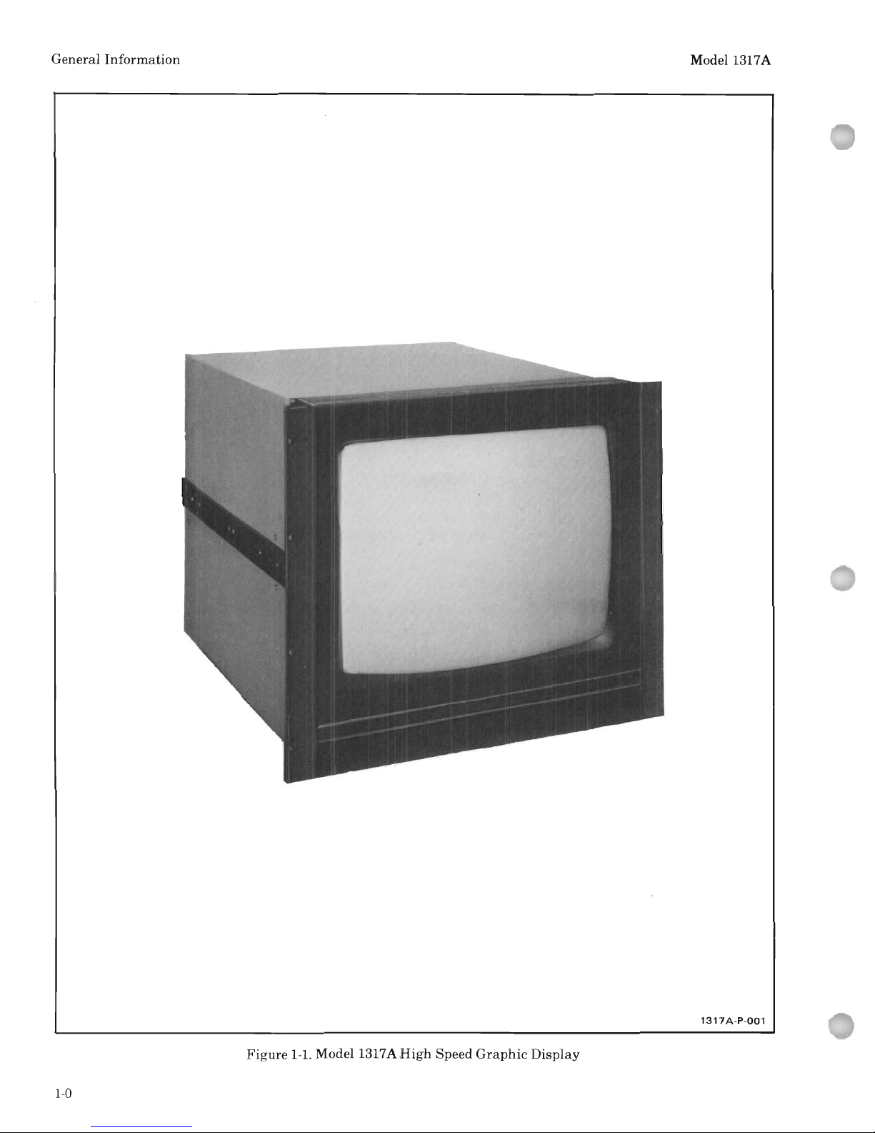
1317A-P-001
Figure 1-1.
Model
1317AHigh
Speed
Graphic
Display
1-0
Page 7
Model 1317A
General
Information
SECTION I
GENERAL INFORMATION
1-1. INTRODUCTION.
1-2.
This
manual
provides
operating
and
servicing
information
for
the
Hewlett-Packard
Model 1317 A
High
Speed
Graphic
Display
(figure
1-1).
The
manual
is divided
into
eight
sections,
each
covering a specific
aspect
of
the
instrument.
All
schematics
are
located
at
the
rear
of
Section VIII.
1-3.
This
section
contains
general
information
per-
taining
to
the
instrument.
Table
1-2
lists
the
abbre-
viations
used
throughout
this
manual,
except
in
Section VI.
The
parts
list
in
Section
VI
is a computer
printout
and
uses
computer
supplied
abbreviations.
1-4.
Available
options
are
listed
and
described
in
Section VII.
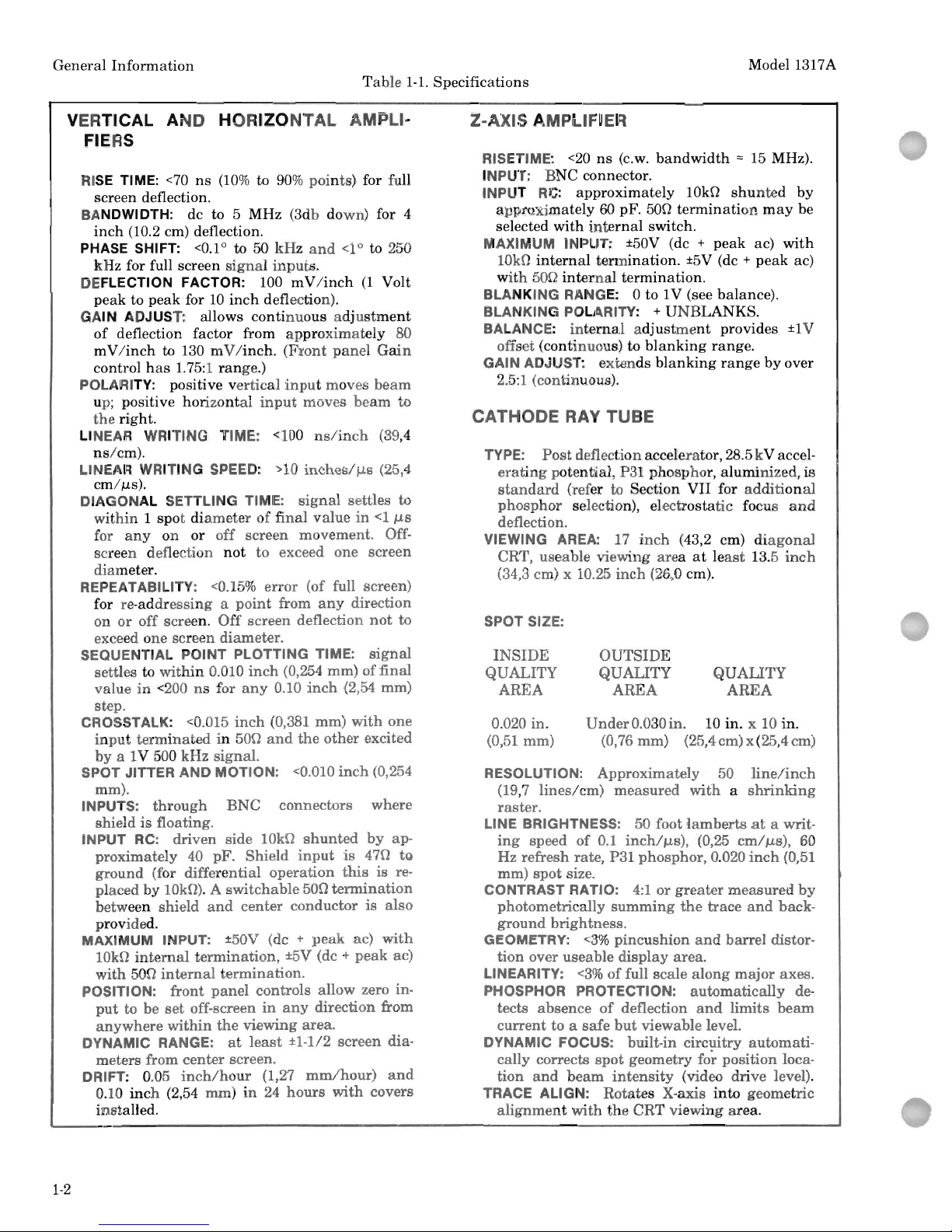
1-5. DESCRIPTION.
1-6.
This
large-screen, general-purpose
graphic
dis-
play
unit
has
been designed for
OEM
systems
ap-
plications. Specifications
are
listed
in
table
1-1.
Suggested
applications
are
listed
in
Section III.
1-7. SPECIAL FEATURES.
1-8.
Input
Modifications.
The
input
circuits to
the
X,
Y,
and
Z amplifiers
are
designed
to
permit
easy
modification for single-ended
or
differential
operation.
Ad~itionally,
the
input
termination
resist-
ance
and
the
input
attenuation
ratio
for
the
X,
Y,
and
Z amplifiers
can
be
changed.
Refer to
the
para-
grahs
on
input
modifications
in
Section III.
1-9.
Dynamic
Focus-astigmatism. Voltages propor-
tional
to
the
position
of
the
CRT
beam
are
applied
to
the
focus
and
astigmatism
elements
of
the
CRT.
This
causes
spot
size
and
shape
to
remain
constant
over
the
CRT
viewing
area.
Focus
is
also
corrected
for
changes
in
intensity
level.
1-10.
Phosphor Protection. A protection circuit
senses slow
or
static
deflection
signals
and
limits
beam
intensity
to
prevent
burning
of
the
CRT
phos-
phor
and
mesh.
1-11. CATHODE-RAY TUBE.
1-12.
The
CRT
has
an
aluminized
P31
phosphor
and
a
usable
viewing
area
of
approximately
13.5
inch
(34,3 cm) x 10.25
inch
(26,0 cm). A 28-kilovolt ac-
celerating
potential
produces a
bright
display
with-
out
harmful
X-rays.
1-13.
Other
phosphors,
as
well
as a number
of
low-
reflection
contrast
filters
are
available
as
standard
options. Refer to Section VII.
1-14. A rim
and
tension
band
are
fitted
around
the
faceplate seal line to provide protection
against
implosion injury.
1-15.
Complete CRT specifications
are
located
in
table
1-1.
1-16. WARRANTY.
1-17.
The
instrument
is certified
and
warranted
as
stated
in
the
front
of
this
manual.
1-18. ACCESSORIES.
1-19.
Hewlett-Packard
has
available
a wide
range
of
test
equipment
and
accessories for use
with
HP
instruments
and
instruments
of
other
manufacturers.
Refer to
the
latest
HP
catalog
or
request
information
from
the
nearest
HP
Sales
/ Service Office.
1-20. INSTRUMENT AND MANUAL
IDEN-
TIFICATION.
1-21.
This
manual
applies directly
to
instruments
with a serial
prefix
as
listed
on
the
title page.
The
serial
prefix is
the
first group
of
digits
in
the
serial
number
(figure
1-2).
The
serial
number
is
on a tag
affixed to
the
rear
panel.
Note
The
warranty
may
be void
if
the
serial
tag
has
been removed
or
mutilated.
1-22.
Technical corrections (if
any)
are
contained
under
errata
on
an
enclosed
manual
changes
sheet
(if any).
1-23. INQUIRIES.
1-24.
Refer
any
questions
regarding
the
manual,
the
change
pages,
or
the
instrument
to
the
nearest
HP
Sales/Service
Office.
Always
identify
the
instru-
ment
by
model
number,
name,
and
serial
number
in
all correspondence. Refer to
the
rear
of
this
manual
for a world-wide
listing
of
HP
Sales
/ Service Offices.
1-1
Page 8
General
Information
Model 1317A
Table
1-1.
Specifications
VERTICAL AND HORIZONTAL AMPLI-
FIERS
1-2
RISE TIME:
<70
ns
(10%
to
90%
points) for full
screen deflection.
BANDWIDTH: dc to 5 MHz (3db down) for 4
inch
(10.2 cm) deflection.
PHASE SHIFT:
<0.10
to 50
kHz
and
<10
to 250
kHz for full screen
signal
inputs.
DEFLECTION FACTOR: 100
mV
linch
(1
Volt
peak
to
peak
for
10
inch
deflection).
GAIN ADJUST: allows
continuous
adjustment
of
deflection factor from
approximately
80
m V
linch
to 130 m V
linch.
(Front
panel
Gain
control
has
1.75:1 range.)
POLARITY: positive vertical
input
mov
es
beam
up; positive
horizontal
input
moves
beam
to
the
right.
LINEAR WRITING TIME:
<100
ns/inch
(39,4
ns/cm).
LINEAR WRITING SPEED:
>10
inchesllLs
(25,4
cmllLs).
DIAGONAL SETTLING TIME:
signal
settles to
within
1 spot
diameter
of
final
value
in
<IlLs
for
any
on
or
off screen movement. Off-
screen deflection
not
to
exceed one
screen
diameter.
REPEATABILITY:
<0.15%
error
(of full screen)
for re-addressing a
point
from
any direction
on
or
off screen.
Off
screen deflection
not
to
exceed one screen
diameter
.
SEQUENTIAL POINT PLOTTING TIME:
signal
settles to
within
0.010
inch
(0,254 mm)
of
final
value
in
<200
ns
for
any 0.10
inch (2,54 mm)
step.
CROSSTALK: <0.015
inch
(0,381 mm)
with
one
input
terminated
in
50n
and
the
other
excited
by a IV
500 kHz signal.
SPOT JITTER AND MOTION:
<0
.010
inc
h (0,254
mm).
INPUTS:
through
BNC connectors where
shield
is
floating.
INPUT
RC:
driven
side
10kn
shunted
by
ap-
proximately
40
pF. Shield
input
is
47n
to
ground
(for differential
operation
this
is
re-
placed
by
10kn). A
switch able
50n
termination
between shield
and
center
conductor
is
also
provided.
MAXIMUM INPUT: ±50V (dc +
peak
ac)
with
10kn
internal
termination,
±5V
(dc +
peak
ac)
with
50n
internal
termination.
POSITION:
front
panel
controls allow zero in-
put
to be
set
off-screen
in
any
direction from
anywhere
within
the
viewing
area
.
DYNAMIC RANGE:
at
least
±1
-1/2
screen
dia-
meters
from
center
screen.
DRIFT: 0.05
inch/hour
(1,27
mm/hour)
and
0.10
inch
(2,54
mm)
in
24
hours
with
covers
installed.
Z-AXIS AMPLIFIER
RISETIME:
<20
ns
(c.w.
bandwidth::
15 MHz).
INPUT:
BNC
connector.
INPUT
RC:
approximately
10kO
shunted
by
approximately
60
pF.
500
termination
may
be
selected
with
internal
switch.
MAXIMUM INPUT: ±50V (dc +
peak
ac)
with
10kO
internal
termination.
±5V
(dc +
peak
ac)
with
500
internal
termination.
BLANKING RANGE: 0 to
IV
(see balance).
BLANKING POLARITY: + UNBLANKS.
BALANCE:
internal
adjustment
provides
±1
V
offset (continuous) to
blanking
range.
GAIN ADJUST:
extends
blanking
range
by
over
2.5:1 (continuous).
CATHODE
RAY
TUBE
TYPE:
Post
deflection accelerator, 28.5 kVaccel-
erating
potential, P31 phosphor, aluminized,
is
standard
(refer to Section
VII
for
additional
phosphor
selection), electrostatic focus
and
deflection.
VIEWING
AREA:
17
inch
(43,2 cm)
diagonal
CRT, useable viewing
area
at
least
13.5
inch
(34,3 cm) x 10.25
inch
(26,0 cm).
SPOT SIZE:
INSIDE
QUALITY
AREA
0.020 in.
(0,51 mm)
OUTSIDE
QUALITY
AREA
QUALITY
AREA
Under
0.030 in. 10 in. x 10 in.
(0,76 mm) (25,4 cm) x (25,4 cm)
RESOLUTION:
Approximately
50
line/inch
(19,7
lines/cm)
measured
with a shrinking
raster.
LINE BRIGHTNESS: 50 foot
lamberts
at
a writ-
ing
speed
of
0.1 inchllLs), (0,25
cmllLs),
60
Hz
refresh
rate, P31
phosphor,
0.020
inch
(0,51
mm)
spot
size.
CONTRAST RATIO:
4:1
or
greater
measured
by
photometrically
summing
the
trace
and
back-
ground
brightness.
GEOMETRY:
<3%
pincushion
and
barrel
distor-
tion
over useable
display
area.
LINEARITY:
<3%
of
full scale
along
major
axes
.
PHOSPHOR PROTECTION:
automatically
de-
tects
absence
of
deflection
and
limits
beam
current
to a
safe
but
viewable level.
DYNAMIC FOCUS: built-in circuitry
automati-
cally corrects
spot
geometry
fo~
position loca-
tion
and
beam
intensity
(video drive level).
TRACE ALIGN:
Rotates
X-axis
into
geometric
alignment
with
the
CRT
viewing
area.
Page 9
Model 1317A
General
Information
Table
1-1.
Specifications
(Cont'd)
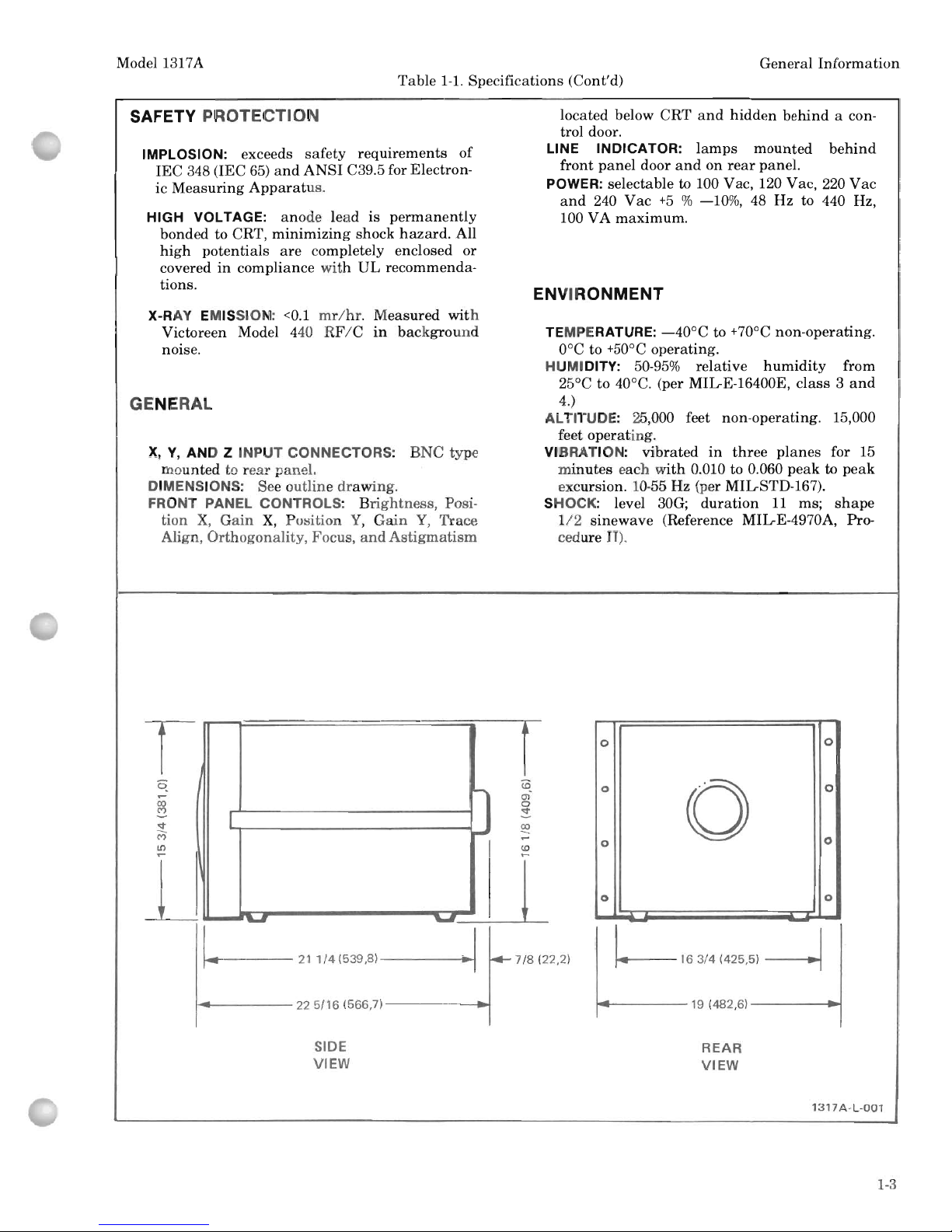
SAFETY PROTECTION
IMPLOSION: exceeds
safety
requirements
of
IEC
348
(IEC
65)
and
ANSI
C39.5 for
Electron-
ic
Measuring
Apparatus.
HIGH VOLTAGE:
anode
lead
is
permanently
bonded
to
CRT,
minimizing
shock
hazard.
All
high
potentials
are
completely
enclosed
or
covered
in
compliance
with
UL
recommenda-
tions.
X-RAY EMISSION:
<0.1
mr/hr.
Measured
with
Victoreen Model 440
RF/C
in
background
noise.
GENERAL
X,
Y,
AND Z INPUT CONNECTORS:
BNC
type
mounted
to
rear
panel.
DIMENSIONS:
See
outline
drawing.
FRONT PANEL CONTROLS:
Brightness,
Posi-
tion
X,
Gain
X,
Position
Y,
Gain
Y,
Trace
Align,
Orthogonality,
Focus,
and
Astigmatism
T
q
.-
~
v
I
M
located
below
CRT
and
hidden
behind
a con-
trol
door.
LINE INDICATOR:
lamps
mounted
behind
front
panel
door
and
on
rear
panel.
POWER:
selectable
to 100
Vac,
120
Vac,
220
Vac
and
240
Vac
+5 % -10%,
48
Hz
to
440 Hz,
100
VA
maximum.
ENVIRONMENT
TEMPERATURE:
-40°C
to
+70°C
non-operating.
O°C
to
+50°C
operating.
HUMIDITY: 50-95%
relative
humidity
from
25°C
to
40°C. (per
MIlrE-16400E,
class 3 and
4.)
ALTITUDE: 25,000 feet
non-operating.
15,000
feet
operating.
VIBRATION:
vibrated
in
three
planes
for 15
minutes
each
with
0.010
to
0.060
peak
to
peak
excursion. 10-55 Hz (per MIlrSTD-167).
SHOCK: level 30G;
duration
11 ms;
shape
1/2
sinewave
(Reference MIlrE-4970A, Pro-
cedure
II).
o
o
o
o
o
o
o
f
~-------l~
i
lJ__
j~
o
o
[
C-16
3/4
(425,5)
~-
~~----211/4(539'8)-----I
..
~1
'-'7/8(22,2)
....
----
225/16
(566,7)
-------I-:-~
SIDE
VIEW
19
(482,6)----~
REAR
VIEW
1317
A-L-001
1-3
Page 10
General
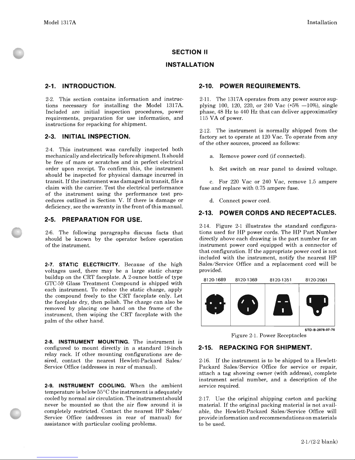
Information
Model 1317A
Table
1-2.
Reference
Designators
and
Abbreviations
REFERENCE DESIGNATORS
A ASSEMBLY
E MISC. ELECTRICAL PART
P
PLUG
U INTEGRATED CIRCUIT
AT
ATTENUATOR
F
FUSE
PS
POWER
SUPPLY
(UNREPAIRABlE)
RESISTIVE TERMINATION
Fl
FILTER
Q
TRANSISTOR
V
VACUUM TUBE, NEON
B MOTOR, FAN
H HARDWARE
R
RESISTOR
BULB, PHOTOCELL, ETC.
BT
BATTERY
J JACK
RT
VR
VOLTAGE REGULATOR
C CAPACITOR
K RELAY
THERMISTOR
(DIODE)
CP COUPLING
l
INDUCTOR
S
SWITCH
W
CABLE
CR
DIODE
lS
SPEAKER
T TRANSFORMER
X SOCKET
Ol
DELAY
LINE
M
METER
TB
TERMINAL
BOARD
Y CRYSTAL
OS DEVICE SIGNALING (LAMP)
MP
MECHANICAL PART
TP
TEST POINT Z
NETWORK
ABBREVIATIONS
A AMPERE(S) F
FARAD(S)
n
NANO (10.9)
rfi
RADIO FREQUENCY
A
AMPERE TURN(S)
FET
FIELD·EFFECT
nc
NORMALLY
CLOSED
INTERFERENCE
ampl
AMPLIFIER(S)
TRANSISTOR(S)
no.
NORMALLY
OPEN
rms
ROOT MEAN SQUARE
assy
ASSEMBLY
G
GIGA (109)
npn
NEGATI VE-POSITIVE-
rwv
REVERSE WORKING
ampltd
AMPLITUDE
gnd
GROUND(ED)
NEGATIVE
VOLTAGE
ns
NANOSECOND
SCR
SILICON CONTROLLED
bd
BOARD(S)
RECTIFIER
bp
BANDPASS
H
HENRY(lES)
P
PICO
(10-12)
sec
SECOND(S)
hr
HOUR(S)
pc
PRINTED (ETCHED)
std
STANDARD
c
CENTI (10-2)
HP
HEWLETT-PACKARD
CIRCUIT(S)
C CARBON
Hz
HERTZ
pi<
PEAK
trmr
TRIMMER
ccw
COUNTERCLOCKWISE
pop
POSITIVE-NEGATIVE-
coax.
COAXIAL
if.
INTERMEDIATE FREQ.
POSITIVE
u
MICRO (10-6)
coef
COEFFICIENT
inti
INTERNAL
p/o
PART
OF
usee MICROSECOND
com
COMMON
pop
PEAK-TO-PEAK
CRT
CATHODE-RAY TUBE
k KILO (10
3
)
prgm
PROGRAM
V VOLTS
cw
CLOCKWISE
Ib
POUND(S)
prv
PEAK INVERSE var
VARIABLE
Ipf
LOW-PASS
FI
L TER(S)
VOLTAGE(S)
d
DECI
(10-1)
ps
PICOSECOND
wI
WITH
dB
DECIBEL
m
MI
LLI (10-3)
pwv
PEAK WORKING
w/o
WITHOUT
M MEGA (10
6
)
VOLTAGE
wiv
WORKING INVERSE
ext
EXTERNAL
ms
MI
LLiSECOND
rf
RADIO FREQUENCY
VOLTAGE
SERIAL
PREFIX
NUMBER
SERIAL
SUFFIX
NUMBER
COMPLETE
SERIAL
NUMBER
Figure
1-2.
Instrument
Serial
Number
1-4
Page 11
Model 1317A
Installation
SECTION II
INST ALLATION
2-1. INTRODUCTION.
2-2.
This
section
contains
information
and
instruc-
tions
necessary
for
installing
the
Model 1317 A.
Included
are
initial
inspection
procedures,
power
requirements,
preparation
for use
information,
and
instructions
for
repacking
for
shipment.
2-3. INITIAL INSPECTION.
2-4.
This
instrument
was
carefully
inspected
both
mechanically
and
electrically before
shipment.
It
should
be free
of
mars
or
scratches
and
in
perfect electrical
order
upon
receipt. To
confirm
this,
the
instrument
should
be
inspected
for
physical
damage
incurred
in
transit.
If
the
instrument
was
damaged
in
transit,
file a
claim
with
the
carrier.
Test
the
electrical
performance
of
the
instrument
using
the
performance
test
pro-
cedures outlined
in
Section
V.
If
there
is
damage
or
deficiency, see
the
warranty
in
the
front
of
this
manual.
2-5. PREPARATION FOR USE.
2-6.
The
following
paragraphs
discuss
facts
that
should
be
known
by
the
operator
before
operation
of
the
instrument.
2-7. STATIC ELECTRICITY.
Because
of
the
high
voltages
used,
there
may
be a large
static
charge
buildup
on
the
CRT
faceplate. A 2-ounce
bottle
of
type
GTC-59
Glass
Treatment
Compound
is
shipped
with
each
instrument.
To reduce
the
static
charge,
apply
the
compound freely to
the
CRT
faceplate
only.
Let
the
faceplate dry,
then
polish.
The
charge
can
also
be
removed
by
placing
one
hand
on
the
frame
of
the
instrument,
then
wiping
the
CRT
faceplate
with
the
palm
of
the
other
hand.
2-8. INSTRUMENT
MOUNTING.
The
instrument
is
configured to
mount
directly
in a standard
19-inch
relay
rack.
If
other
mounting
configurations
are
de-
sired,
contact
the
nearest
Hewlett-Packard
Sales/
Service Office
(addresses
in
rear
of
manual).
2-9. INSTRUMENT COOLING.
When
the
ambient
temperature
is
below 55°C
the
instrument
is
adequately
:
cooled
by
normal
air
circulation.
The
instrument
should
never
be
mounted
so
that
the
air
flow
around
it
is
completely restricted.
Contact
the
nearest
HP
Sales/
Service Office
(addresses
in
rear
of
manual)
for
.
assistance
with
particular
cooling problems.
2-10. POWER REQUIREMENTS.
2-11.
The
1317 A
operates
from
any
power
source sup-
plying
100, 120, 220,
or
240
Vac
(+5%
-10%),
single
phase,
48 Hz to 440 Hz
that
can
deliver
approximatley
115 VA
of
power.
2-12.
The
instrument
is
normally
shipped
from
the
factory
set
to
operate
at
120 Vac.
To
operate
from
any
of
the
other
sources, proceed
as
follows:
a. Remove power cord (if connected).
b.
Set
switch
on
rear
panel
to
desired voltage.
c.
For
220
Vac
or 240 Vac,
remove
1.5
ampere
fuse
and
replace
with
0.75
ampere
fuse.
d.
Connect
power cord.
2-13. POWER CORDS AND RECEPTACLES.
2-14.
Figure
2-1
illustrates
the
standard
configura-
tions
used
for
HP
power cords.
The
HP
Part
Number
directly
above
each
drawing
is
the
part
number
for
an
instrument
power cord
equipped
with a connector
of
that
configuration.
If
the
appropriate
power
cord
is
not
included
with
the
instrument,
notify
the
nearest
HP
Sales
/ Service Office
and a replacement
cord will be
provided.
8120-1689 8120-1369
8120-1351 8120-2061
•••
STD-8-2878-07 -76
Figure
2-1.
Power
Receptacles
2-15. REPACKING FOR SHIPMENT.
2-16.
If
the
instrument
is
to
be
shipped
to
a Hewlett-
Packard
Sales
/ Service Office for service
or
repair,
attach a tag
showing
owner
(with
address),
complete
instrument
serial
number,
and a description
of
the
service required.
2-17.
Use
the
original
shipping
carton
and
packing
material.
If
the
original
packing
material
is
not
avail-
able,
the
Hewlett-Packard
Sales/Service
Office will
provide
information
and
recommendations
on
materials
to be used.
2-1/(2-2
blank)
Page 12

•
Page 13
Model 1317A
Operation
SECTION III
OPERATION
3-1.
INTRODUCTION.
3-2.
This
operating
section
explains
the
functions
of
all
external
controls
and
connectors
of
the
Model
1317 A.
It
describes
typical
operating
modes
and
covers
operator
maintenance
and
operating
instructions
for
most
applications.
3-3. INSTRUMENT CAPABILITIES.
3-4.
The
Model 1317A
is
designed
so
that
easy
customer-installed
modifications
adapt
the
instrument
for a wide
variety
of
applications.
Refer to
Section
VII
for details.
I
WARNING
I
Dangerous
voltages
capable
of
causing
death
are
present
in
this
instrument.
The
following
internal
adjustments
are
outlined
in
Section V
of
this
manual
and
should
be
made
by
qualified service per-
sonnelonly.
3-5. SELECTABLE INPUT IMPEDANCE.
Three
manual
switches
permit
selection
of
either
50
ohms
or
10 kil-
ohms
input
impedance.
One
switch
is
located
on
X-
axis
Amplifier
Assembly
AI,
another
is
on
Y-axis
Amplifier
Assembly
A3,
and
the
third
is
on
Z-axis
Amplifier
Assembly
A5.
3-6. ADJUSTABLE Z-AXIS GAIN AND BALANCE.
These two
adjustments
are
factory
set
to
give
optimum
Z-axis
operation
and
have
no
bearing
on
calibration
of
the
instruments
after
repair
or
replacement
of
parts.
Gain
adjustment
may
be
set
to
reduce Z-axis
amplifier
gain
by a
factor
of
2.5.
Balance
control
is
used
to
adjust
offset
of
positive
or
negative
blanking
voltage
levels
by
±1
V.
These
adjustments
are
optional
to
the
user
according
to
Z-axis
voltage
inputs
and
attenuation
factors required
by
a specific
application.
The
phosphor
protection
circuit
pro-
tects
the
CRT
against
a
number
of
malfunctions.
Unless
it
is
absolutely
necessary
to
obtain a brighter
display
for
static
or
very
slow deflection
signals,
or
if
the
time
constants
of
the X-and
Y-input
signals
cause
nonuniform
inten-
sity, leave
PHOSPHOR
PROTECTION
switch
in
the
ON
position.
3-7. PHOSPHOR PROTECTION CIRCUIT. A
phosphor
protection circuit
is
provided
which
can
be
enabled
or
disabled
with
an
internal
manual
switch.
In
opera-
tion,
the
phosphor
protection
circuit
detects
absence
of
deflection
signals
(or slow-speed deflection)
and
reduces
CRT
cathode
current
to a safe
level.
When
deflection
signals
are
restored
(or speed
increased
beyond
damage
limit), full
CRT
beam
current
is
also
restored.
3-8. OPERATOR MAINTENANCE.
3-9.
Operator
maintenance
should
be
limited
to
pre-
operational
adjustment
(figure
3-2)
and
to
exterior
cleaning
of
the
instrument.
Occasional
cleaning
of
the
CRT
faceplate
should
be done
with
alcohol
and
a soft,
nonabrasive
wiping
material.
Plastic
instrument
covers (if used)
can
be
cleaned
with
any
mild
house-
hold
detergent.
Gliffi
Do
not
use
coarse
substances
or
cleaning
tissues
containing
glass
reinforcing
fibers
on
CRT
filters.
The
filters
are
plastic
and
easily
scratched.
3-10.
CONTROLS
AND
CONNECTORS.
3-11.
Front-
and
rear-panel
controls
and
connectors
are
illustrated
and
described
in
figure
3-1.
3-12. OPERATING PROCEDURES.
3-13.
Figures
3-2
and
3-3
contain
step-by-step opera-
ting
procedures.
Index
numbers
on
the
illustrations
correspond to
step
numbers
in
the
instructions.
Only
basic
techniques
are
covered.
These
techniques
can
be modified or
combined
to provide a
number
of
unique
operating
requirements.
3-1
Page 14
Operation
Model 1317A
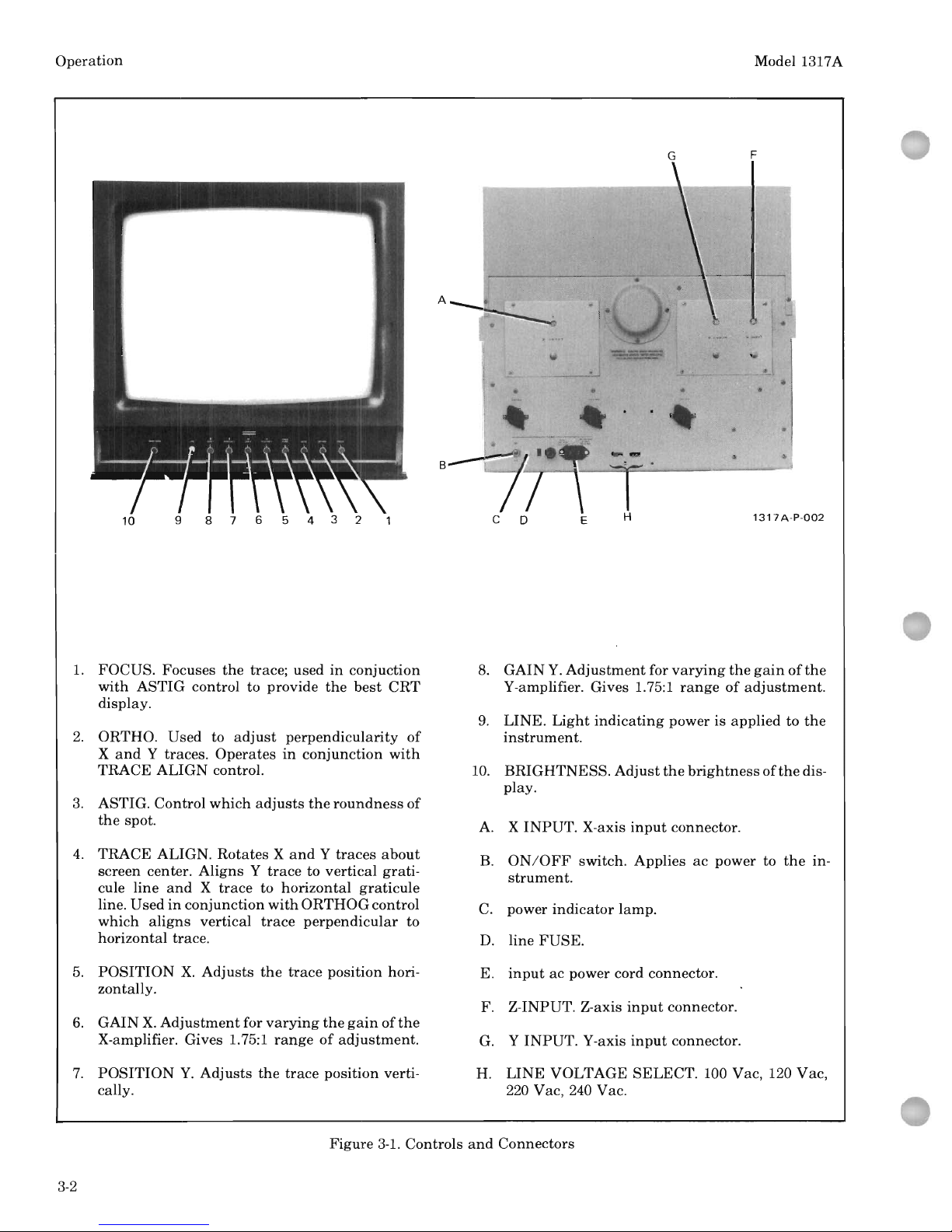
G
F
10
98765432
C D
E
1317
A -
P-002
1.
FOCUS. Focuses
the
trace; used
in
conjuction 8.
GAIN
Y.
Adjustment
for
varying
the
gain
of
the
with
ASTIG
control to provide
the
best
CRT
V-amplifier. Gives 1.75:1
range
of
adjustment.
display.
9.
LINE.
Light
indicating
power
is
applied
to
the
2.
ORTHO. Used to
adjust
perpendicularity
of
instrument.
X
and
Y traces.
Operates
in
conjunction
with
TRACE
ALIGN
control.
10
. BRIGHTNESS.
Adjust
the
brightness
of
the
dis-
play.
3.
ASTIG. Control
which
adjusts
the
roundness
of
the
spot.
A.
X
INPUT.
X-axis
input
connector.
4.
TRACE ALIGN. Rotates X
and Y traces
about
B.
ON/OFF
switch. Applies
ac
power to
the
in-
screen center. Aligns Y
trace
to vertical grati-
strument.
cule line
and X trace
to
horizontal
graticule
line. Used
in
conjunction
with
ORTHOG control
C.
power
indicator
lamp.
which
aligns
vertical
trace
perpendicular
to
horizontal trace.
D.
line
FUSE.
5.
POSITION
X.
Adjusts
the
trace
position hori-
E.
input
ac
power cord connector.
zontally.
F.
Z-INPUT. Z-axis
input
connector.
6.
GAIN
X.
Adjustment
for
varying
the
gain
of
the
X-amplifier. Gives 1.75:1
range
of
adjustment.
G.
Y
INPUT.
Y-axis
input
connector.
7.
POSITION
Y.
Adjusts
the
trace
position verti-
H.
LINE
VOLTAGE SELECT. 100 Vac, 120 Vac,
cally.
220 Vac,
240
Vac.
Figure
3-1.
Controls
and
Connectors
3-2
Page 15
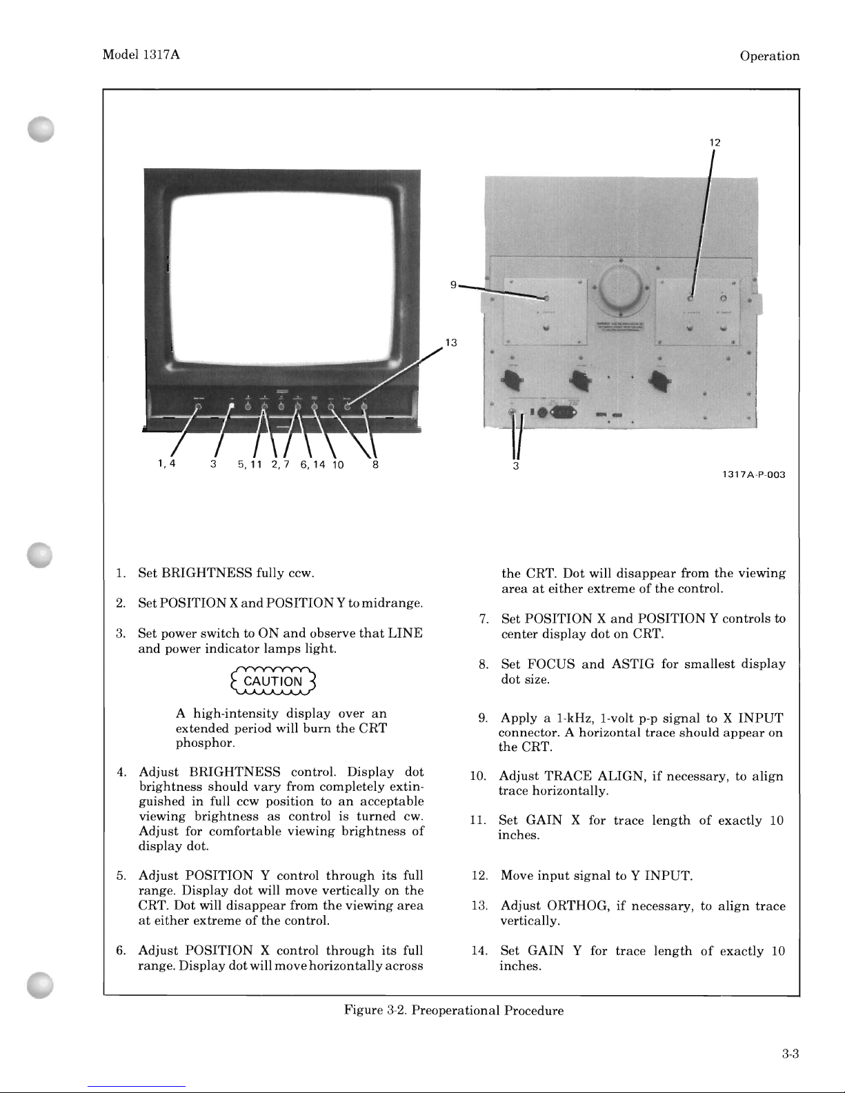
Model 1317A
3
5,112,7
6,1410
8
1.
Set
BRIGHTNESS
fully ccw.
2.
Set
POSITION X and
POSITION
Y to
midrange.
3. Set power
switch
to
ON
and
observe
that
LINE
and
power
indicator
lamps
light.
~
A
high-intensity
display
over
an
extended period will
burn
the
CRT
phosphor.
4.
Adjust
BRIGHTNESS
control.
Display
dot
brightness
should
vary
from completely extin-
guished
in
full ccw
position
to
an
acceptable
viewing
brightness
as
control
is
turned
cwo
Adjust
for comfortable viewing
brightness
of
display
dot.
5.
Adjust
POSITION
Y control
through
its
full
range.
Display
dot
will move
vertically
on
the
CRT. Dot will
disappear
from
the
viewing
area
at
either
extreme
of
the
control.
6.
Adjust
POSITION
X control
through
its
full
range.
Display
dot will
move
horizontally
across
13
Operation
12
--
1317A-P-003
the
CRT.
Dot
will
disappear
from
the
viewing
area
at
either
extreme
of
the
control.
7.
Set
POSITION X and
POSITION
Y controls to
center
display
dot
on
CRT.
8.
Set
FOCUS
and
ASTIG
for
smallest
display
dot size.
9.
Apply
a I-kHz, I-volt p-p
signal
to X
INPUT
connector. A
horizontal
trace
should
appear
on
the
CRT.
10.
Adjust
TRACE
ALIGN,
if
necessary, to
align
trace
horizontally.
11.
Set
GAIN
X for
trace
length
of
exactly
10
inches.
12. Move
input
signal
to Y
INPUT.
13.
Adjust
ORTHOG,
if
necessary,
to
align
trace
vertically.
14.
Set
GAIN
Y for
trace
length
of
exactly
10
inches.
Figure
3-2.
Preoperational
Procedure
3-3
Page 16
Operation
3-4
••
4
I
BAL
CONTROL
A5R8
INSIDE ON
A5
BOARD
~-.----
~
-,
-&
I
..
J
- -
.,
1317
A-P-004
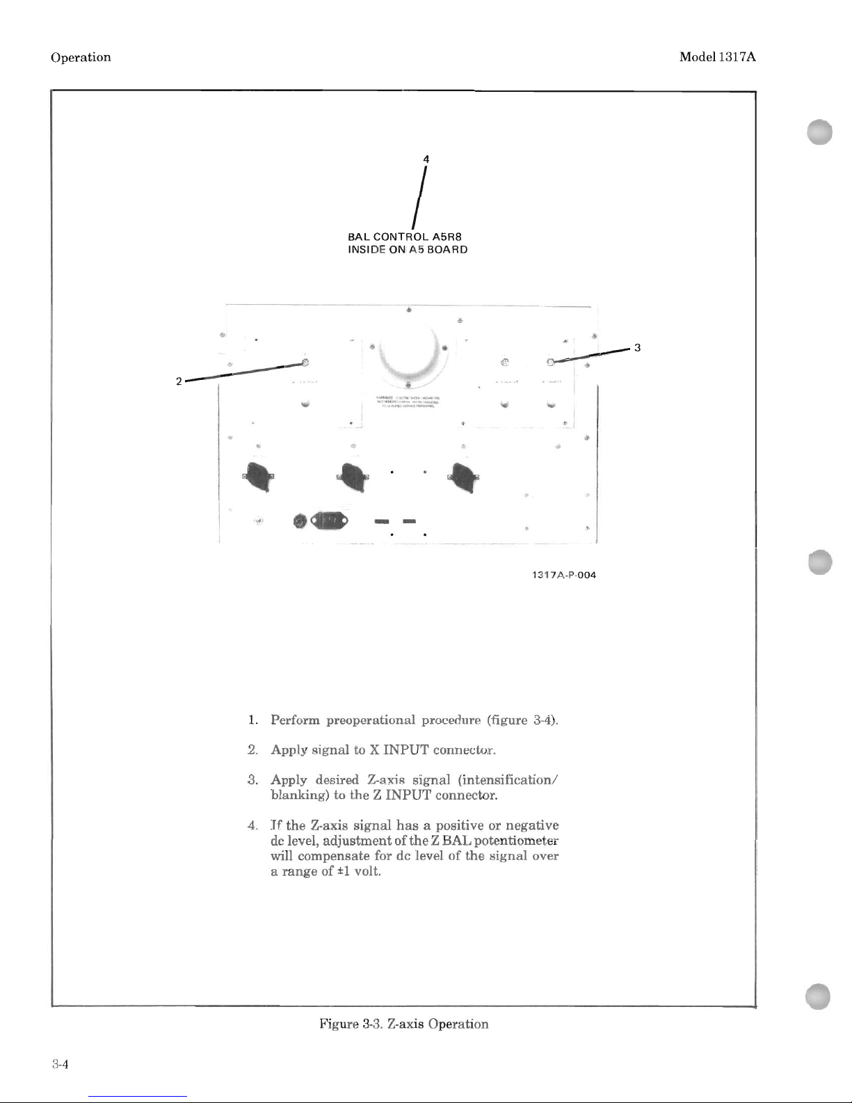
1. Perform
preoperational
procedure (figure
3-4).
2.
Apply
signal
to X
INPUT
connector.
3.
Apply desired Z-axis
signal
(intensification/
blanking)
to
the Z INPUT
connector.
4.
If
the
Z-axis
signal
has
a positive
or
negative
dc level,
adjustment
of
the Z BAL
potentiometer
will
compensate
for dc level
of
the
signal
over
a
range
of
±1
volt.
Figure
3-3
. Z-axis Operation
Model 1317A
Page 17
Model 1317A
Theory
SECTION IV
PRINCIPLES OF OPERATION
4-1. INTRODUCTION.
4-2.
This
section
contains
function
descriptions
of
Model 1317 A, keyed to
an
overall
block
diagram.
The
block
diagram
and
schematics
are
located
in
Section VIII.
4-3. BLOCK DIAGRAM DISCUSSION.
4-4.
This
discussion
illustrates
the
function
of
each
circuit
group
(block)
and
the
relationship
of
the
blocks to
each
other.
It
is
based
on
the
overall
block
diagram,
figure 8-2.
The
conditioning
and
calibrating
controls,
as
shown
on
the
block
diagram,
illustrate
the
association
of
the
control
with a particular
block
and
are
not
necessarily
an
accurate
representation
of
the
control's action.
4-5. LOW VOLTAGE POWER SUPPLIES.
4-6.
This
block
(All)
provides
operating
power
to
all
the
other
blocks,
including
the
high
voltage
power
supply
and
some
of
the
CRT
elements.
Three
regu-
lated
dc
outputs
are
provided: +250 V,
+15
V,
and
-15
V.
The
+250 V supply
and
the
-15 V supply
are
adjustable.
The
+15 V supply
is
referenced
to
the
-15
V supply.
Several
other
voltages
are
derived
from
the
+250 V supply
by
means
of
voltage
dividers
and
avalanche
diodes.
Additionally,
an
unregulated
dc
output
to
the
high
voltage
oscillator
and
a 6.3
Vac
output
to
the
CRT
filament
are
provided.
4-7. HIGH VOLTAGE POWER SUPPLY.
4-8.
The
high
voltage
power
supply
(on A12
and
A13)
provides
the
high
operating
potentials
for
the
CRT.
The
rf
output
of
the
high
voltage
oscillator
is
stepped up
by
the
high
voltage
transformer
and
con-
ditioned
by
the
other
components
on
A12. A
sample
of
the
high
voltage
output
drives
the
error
detector.
The
error detector
controls
the
conduction
angle
of
the
high
voltage
oscillator
to
accomplish
regulation.
4-9. DEFLECTION SYSTEM.
4-10.
The
X-axis
amplifiers
(on
Al
and
A2)
and
the
Y-axis amplifiers (on A3
and
A4)
are
identical.
They
drive
the
horizontal
and
vertical
deflection
plates
of
the
CRT
proportionally
to
the
signals
applied
to
the
X
INPUT
and Y INPUT.
4-11. FOCUS AND ASTIGMATISM CIRCUITS.
4-12.
Samples
from
the X and
Y amplifiers, pro-
portional to
the
CRT
beam
position,
drive
the
focus
and
astigmatism
circuits (on A6).
These
circuits
develop correction
voltages
for
the
focus
and
astig-
matism
elements
of
the
CRT.
The
astigmatism
element
is
directly controlled
by
the
output
of
the
astigmatism
driver.
The
focus
element
is
connected
to
the
-3400 V output
of
the
high
voltage
power
supply.
This
supply
is
returned
to
(and
controlled
by)
the
output
of
the
focus driver.
The
focus
driver
also receives a
sample
from
the
Z-axis
amplifier
and
causes
focus corrections for
changes
in
beam
inten-
sity.
4-13. PHOSPHOR PROTECTION CIRCUITS.
4-14.
The
phosphor
protect
control
circuits
(on
Al
and
A3) detect
static
or slow
moving
deflection
voltages
and
activate
the
phosphor
protection
circuit
(on A5).
The
phosphor
protection
circuit
limits
the
output
of
the
Z-azis
amplifier
and
protects
the
CRT
mesh
and
phosphor
from
damage
that a static,
high-
intensity
beam
could cause.
4-15. Z-AXIS AMPLIFIER.
4-16.
The
high
voltage
supply
for
the
CRT
control
grid
is
returned
to
(and
controlled by)
the
output
of
the
Z-axis
amplifier
(on A6).
Consequently,
the
volt-
age
applied to
the Z INPUT
controls
CRT
beam
intensity.
The
Z-axis
amplifier
can
be
switched
to
permit
blanking
by
either
a positive
or
negative
voltage
at
the Z INPUT.
4-17. CIRCUIT DETAILS.
4-18. PHOSPHOR PROTECT CIRCUITS.
Phosphor
protect circuits
in
the X axis
and Y axis
are
identical
in
operation
so
only
the
X-axis circuits will be describ-
ed
(schematics 1 and
2).
4-19. Excessive
intensity
caused
by
a slow-moving
or
static
beam
can
cause
damage
to
the
CRT
ex-
pansion
mesh
or
phosphors.
When
deflection
speeds
are
reduced to a
potentially
harmful
level (less
than
approximately
76
mm/ms
(3 in.!
ms),
the
phosphor
protect circuits
limit
CRT
cathode
current.
This
current
limiting
action
occurs
because
of
circuit
actions
described below.
4-20. Differential output, from
the
X-axis
voltage
differential
amplifier
stage
(schematic
1),
is
applied
to
X-axis
emitter
follower
stage
(schematic
2).
Differ-
ential
output
of
this
stage
is
proportional
to
the
beam
position
in
the
X-axis direction,
and
is
applied
to
the
voltage
sensor
stage. A voltage
change
at
the
col-
lector
of
either
voltage
sensor
reduces
the
voltage
on
A1C19.
When
the
voltage
on
A1C19
is
sufficiently
reduced,
the
phosphor
protect
control
is
activated
and
produces a positive
voltage
at
its
output.
4-1
Page 18
Theory
Model 1317A
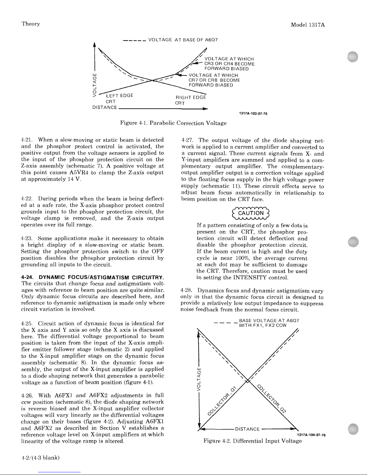
_____
VOLTAGE
AT
BASE OF
A6Q7
w
<.!J
«
I-
~
o
>
."
II
VOLTAGE
AT
WHICH
~
CR3 OR CR4 BECOME
7:;'
FORWARD
BIASED
~--
VOLTAGE
ATWHICH
CR7 OR CR8 BECOME
FORWARD
BIASED
RIGHT
EDGE
CRT
DISTANCE
_____________
.~
1317A-103-07-76
Figure
4-1.
Parabolic
Correction
Voltage
4-21. When a slow-moving
or
static
beam
is
detected
and
the
phosphor
protect
control
is
activated,
the
positive
output
from
the
voltage
sensors
is
applied
to
the
input
of
the
phosphor
protection
circuit
on
the
Z-axis
assembly
(schematic
7). A positive
voltage
at
this
point
causes
A5VR4
to
clamp
the Z-axis
output
at
approximately
14 V.
4-22.
During
periods
when
the
beam
is
being
deflect-
ed
at a safe
rate,
the
X-axis
phosphor
protect
control
grounds
input
to
the
phosphor
protection
circuit,
the
voltage
clamp
is removed,
and
the
Z-axis
output
operates
over
its
full
range.
4-23.
Some
applications
make
it
necessary
to
obtain
a
bright
display
of
a slow-moving
or
sta
tic
beam.
Setting
the
phosphor
protection
switch
to
the
OFF
position
disables
the
phosphor
protection
circuit
by
grounding
all
inputs
to
the
circuit.
4-24. DYNAMIC FOCUS/ASTIGMATISM CIRCUITRY.
The
circuits
that
change
focus
and
astigmatism
volt-
ages
with
reference
to
beam
position
are
quite
similar.
Only
dynamic
focus
circuits
are
described here,
and
reference
to
dynamic
astigmatism
is
made
only
where
circuit
variation
is
involved
.
4-25.
Circuit
action
of
dynamic
focus
is
identical
for
the X axis
and Y axis
so
only
the X axis
is
discussed
here.
The
differential
voltage
proportional
to
beam
position
is
taken
from
the
input
of
the
X-axis
ampli-
fier
emitter
follower
stage
(schematic
2)
and
applied
to
the
X-input
amplifier
stage
on
the
dynamic
focus
assembly
(schematic
8).
In
the
dynamic
focus as-
sembly,
the
output
of
the
X-input
amplifier
is
applied
to a diode
shaping
network
that
generates a parabolic
voltage
as a function
of
beam
position
(figure 4-1).
4-26. With
A6FXl
and
A6FX2
adjustments
in
full
ccw position
(schematic
8),
the
diode
shaping
network
is reverse
biased
and
the
X-input
amplifier
collector
voltages
will
vary
linearly
as
the
differential
voltages
change
on
their
bases
(figure 4-2).
Adjusting
A6FXl
and
A6FX2
as
described
in
Section V establishes
a
reference
voltage
level
on
X-input
amplifiers
at
which
linearity
of
the
voltage
ramp
is
altered.
4-2
/ (
4-3
blank)
4-27.
The
output
voltage
of
the
diode
shaping
net-
work
is
applied
to a current
amplifier
and
converted
to
a
current
signal.
These
current
signals
from X-and
Y-input
amplifiers
are
summed
and
applied
to
a com-
plementary
output
amplifier.
The
complementary-
output
amplifier
output
is
a correction
voltage
applied
to
the
floating
focus
supply
in
the
high
voltage
power
supply
(schematic
11).
These
circuit
effects
serve
to
adjust
beam
focus
automatically
in
relationship
to
beam
position
on
the
CRT
face.
Glli§B
If
a
pattern
consisting
of
only
a few
dots
is
present
on
the
CRT,
the
phosphor
pro-
tection
circuit
will
detect
deflection
and
disable
the
phosphor
protection
circuit.
If
the
beam
current
is
high
and
the
duty
cycle is
near
100%,
the
average
current
at
each
dot
may
be
sufficient
to
damage
the
CRT. Therefore,
caution
must
be
used
in
setting
the
INTENSITY
control.
4-28.
Dynamics
focus
and
dynamic
astigmatism
vary
only
in
that
the
dynamic
focus
circuit
is
designed
to
provide a
relatively
low
output
impedance
to
suppress
noise feedback from
the
normal
focus circuit.
____
BASE
VOLTAGE
AT
A6Q7
WITH
FX1,
FX2
CCW
1317A-104-07-76
Figure
4-2.
Differential
Input
Voltage
Page 19

Page 20
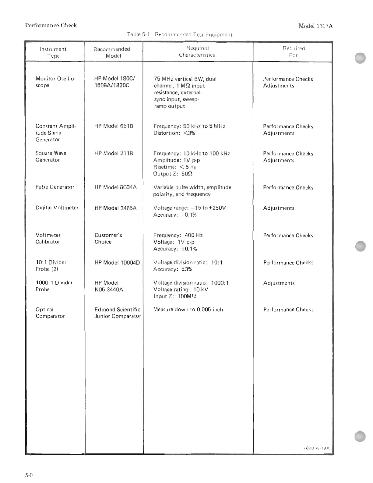
Performance
Check
Model 1317A
Table 5-
1.
Recommended Tes[ Equipment
Instrument
Recomm
en
ded
Requ ireu
R
eq
uir
ed
Type
Model
Characteristics
For
Monitor
Oscillo-
HP
Model 180C/
75
MHz
vertical BW, dual
Performance Checks
scope
1808A/1820C
channel, 1
Mn
input
Adjustments
resistance, external-
sync
input,
sweep-
ramp
output
Constant
Ampli-
HP
Model 651 B
Frequency: 50 kHz
to
5 MHz
Performance Checks
tude Signal
Distortion:
<3%
Adjustments
Generator
Square
Wave
HP
Model 211B
Frequency:
10kHz
to
100 kHz
Performance Checks
Generator
Amplitude:
lV
POp
Adjustments
Risetime: < 5
ns
Output
Z:
50n
Pulse
Generator
HP
Model
8004A
Variable pulse
width,
amplitude,
Performance Checks
polarity, and
frequency
Digital
Voltmeter
HP
Model
3465A
Voltage range:
-15
to
+250V
Adjustments
Accuracy: ±0.1%
Voltmeter
Customer's
Frequency:
400
Hz
Performance Checks
Calibrator Choice
Voltage:
lV
POp
Accuracy: ±0.1%
10:1 Divider
HP
Model
100040
Voltage division ratio:
10: 1
Performance Checks
Probe (2)
Accu racy: ±
3%
1000:1 Divider
HP
Model
Voltage division ratio:
1000: 1
Adjustments
Probe
K05-3440A
Voltage rating:
10
kV
Input
Z:
100Mn
Optical
Edmond
Scientific
Measure
down
to
0.005 inch
Performance Checks
Comparator
Junior
Comparator
7000
-A ·
19A
5-0
Page 21
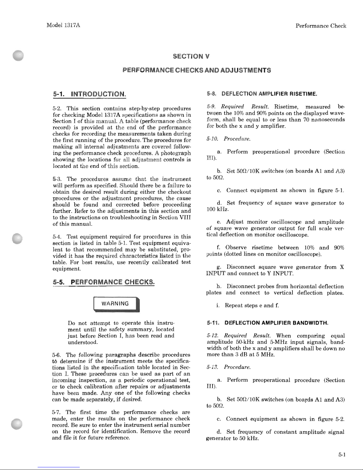
Model 1317A
Performance
Check
SECTION V
PERFORMANCE
CHECKSAND
ADJUSTMENTS
5-1. INTRODUCTION.
5-2.
This
section
contains
step-by-step procedures
for
checking
Model 1317 A specifications
as
shown
in
Section I
of
this
manual. A table
(performance
check
record)
is
provided
at
the
end
of
the
performance
checks for
recording
the
measurements
taken
during
the
first
running
of
the
procedure.
The
procedures for
making
all
internal
adjustments
are
covered follow-
ing
the
performance
check procedures. A
photograph
showing
the
locations
for
all
adjustment
controls
is
located
at
the
end
of
this
section.
a-3.
The
procedures
assume
that
the
instrument
will perform
as
specified.
Should
there
be a failure
to
obtain
the
desired
result
during
either
the
checkout
procedures
or
the
adjustment
procedures,
the
cause
should
be
found
and
corrected before
proceeding
further. Refer to
the
adjustments
in
this
section
and
to
the
instructions
on
troubleshooting
in
Section
VIII
of
this
manual.
5-4.
Test
equipment
required
for procedures
in
this
section
is
listed
in
table
5-1.
Test
equipment
equiva-
lent
to
that
recommended
may
be
substituted,
pro-
vided
it
has
the
required
characteristics
listed
in
the
table.
For
best
results,
use
recently
calibrated
test
equipment.
5-5. PERFORMANCE CHECKS.
WARNING I
Do
not
attempt
to
operate
this
instru-
ment
until
the
safety
summary,
located
just
before
Section
I,
has
been
read
and
understood.
5-6.
The
following
paragraphs
describe
procedures
t6
determine
if
the
instrument
meets
the
specifica-
tions listed
in
the
specification
table
located
in
Sec-
tion
1.
These
procedures
can
be
used
as
part
of
an
incoming
inspection,
as
a periodic
operational
test,
or
to check
calibration
after
repairs
or
adjustments
have
been
made.
Anyone
of
the
following
checks
can
be
made
separately,
if
desired.
5-7.
The
first
time
the
performance
checks
are
made,
enter
the
results
on
the
performance
check
record. Be
sure
to
enter
the
instrument
serial
number
on
the
record for identification. Remove
the
record
and
file
it
for
future
reference.
5-8. DEFLECTION AMPLIFIER RISETIME.
5-9.
Required Result. Risetime,
measured
be-
tween
the
10%
and
90%
points
on
the
displayed
wave-
form,
shall
be
equal
to
or
less
than
70
nanoseconds
for
both
the x and
y amplifier.
5-10.
Procedure.
a.
Perform
preoperational
procedure (Section
III).
b.
Set
50{2110K
switches
(on
boards
Al
and
A3)
to 500.
c.
Connect
equipment
as
shown
in
figure 5-1.
d.
Set
frequency
of
square
wave
generator
to
100 kHz.
e.
Adjust
monitor
oscilloscope
and
amplitude
of
square
wave
generator
output
for full
scale
ver-
tical deflection
on
monitor
oscilloscope.
f.
Observe risetime
between
10%
and
90%
points
(dotted
lines
on
monitor
oscilloscope).
g.
Disconnect
square
wave
generator
from X
INPUT
and
connect
to Y
INPUT.
h.
Disconnect
probes from
horizontal
deflection
plates
and
connect
to
vertical
deflection
plates.
i.
Repeat
steps e and
f.
5-11. DEFLECTION AMPLIFIER BANDWIDTH.
5-12.
Required Result.
When
comparing
equal
amplitude
50-kHz
and
5-MHz
input
signals,
band-
width
of
both
the x and y amplifiers
shall
be
down
no
more
than
3 dB
at
5 MHz.
5-13.
Procedure.
a.
Perform
preoperational
procedure (Section
III).
b.
Set
500/10K
switches
(on
boards
Al
and
A3)
to
500.
c.
Connect
equipment
as
shown
in
figure 5-2.
d.
Set
frequency
of
constant
amplitude
signal
generator
to 50 kHz.
5-1
Page 22
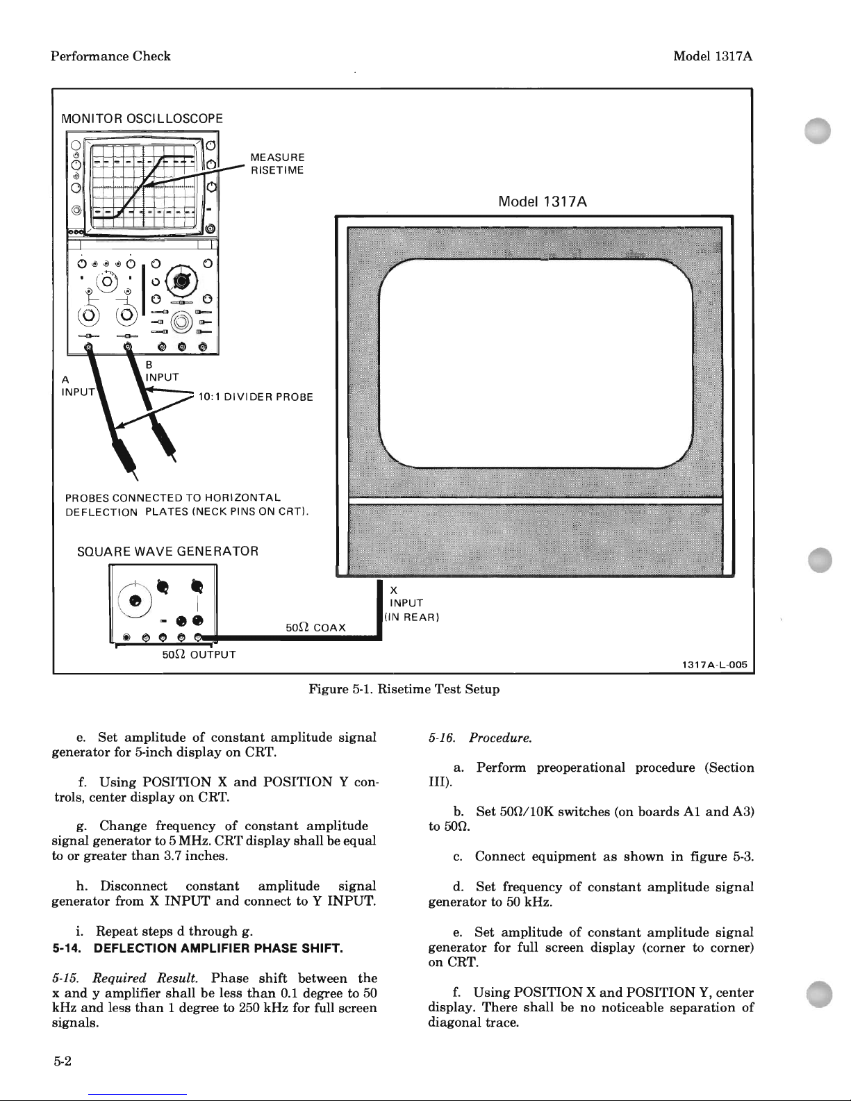
Performance
Check
MONITOR
OSCI
LLOSCOPE
0 ' /
(J
@
1
1-t-+-t-+--t---1
r--;~-I
1
C) I
f----+-+-+----+--'
~
-+-t-H
@
o
@
MEASURE
RISETIME
10:1
DIVIDER
PROBE
PROBES
CONNECTED
TO
HORIZONTAL
DEFLECTION
PLATES
(NECK
PINS ON
CRT).
SQUARE
WAVE
GENERATOR
I
__
0 1
....
son
COAX
@
@)
e e
son
OUTPUT
X
INPUT
(IN
REAR)
Model 1317A
Model 1317A
1317
A-L-005
Figure
5-1.
Risetime
Test
Setup
e.
Set
amplitude
of
constant
amplitude
signal
generator
for 5-inch
display
on
CRT.
f.
Using
POSITION X and
POSITION
Y con-
trols, center
display
on
CRT.
g.
Change
frequency
of
constant
amplitude
signal
generator
to 5 MHz. CRT
display
shall
be
equal
to or
greater
than
3.7 inches.
h. Disconnect
constant
amplitude
signal
generator
from X
INPUT
and
connect
to
Y
INPUT.
i.
Repeat
steps d through
g.
5-14. DEFLECTION AMPLIFIER PHASE SHIFT.
5-15.
Required Result.
Phase
shift
between
the
x
and
y amplifier
shall
be
less
than
0.1 degree
to
50
kHz
and
less
than
1 degree to 250 kHz for full
screen
signals
.
5-2
5-
16.
Procedure.
a.
Perform
preoperational
procedure (Section
III).
b.
Set
500/10K
switches (on
boards
Al
and
A3)
to 500.
c.
Connect
equipment
as
shown
in
figure
5-3.
d.
Set
frequency
of
constant
amplitude
signal
generator
to 50 kHz.
e.
Set
amplitude
of
constant
amplitude
signal
generator
for full screen
display
(corner
to
corner)
on
CRT.
f.
Using
POSITION X and
POSITION
Y,
center
display.
There
shall
be
no
noticeable
separation
of
diagonal
trace.
Page 23
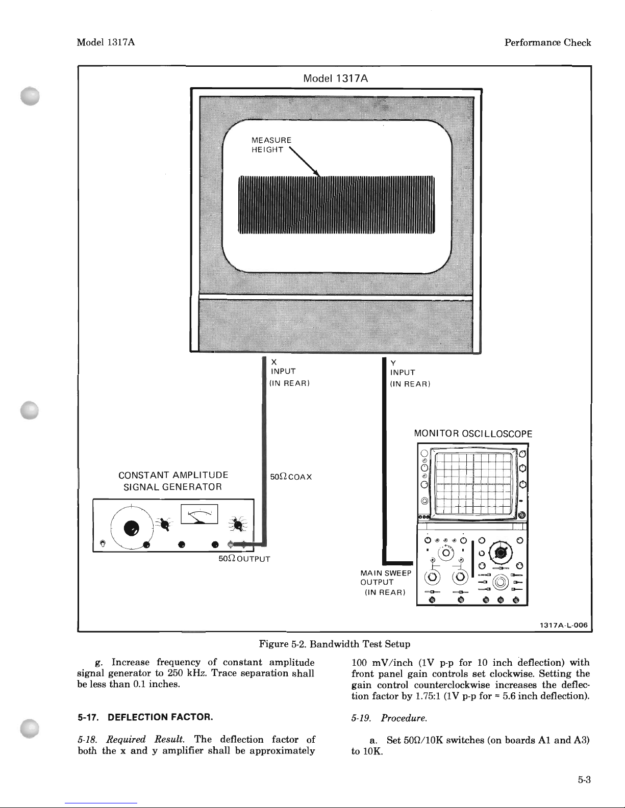
Model 1317A
Performance Check
Model 1317A
CONSTANT
AMPLITUDE
SIGNAL
GENERATOR
MEASURE
HEIGHT
X
INPUT
(IN
REAR)
50nCOAX
fe\~[Sg
~
~
~
..
--T~
50nOUTPUT
y
INPUT
(IN
REAR)
MAIN
SWEEP
OUTPUT
(IN
REAR)
MONITOR
OSCI
LLOSCOPE
0'
/
C)
@
()
0
@
0
10
@
-
iiiiiii
/
e
I I I
O®®'OIO@O
·
@.
0_
@
~
,
0=-=0
~
~
~@;:
e
~
•
0
to
1317A-L-006
Figure
5-2.
Bandwidth
Test
Setup
g. Increase frequency
of
constant
amplitude
signal
generator to 250 kHz.
Trace
separation
shall
be less
than
0.1
inches.
5-17. DEFLECTION FACTOR.
5-18.
Required Result.
The
deflection factor
of
both
the x and
y amplifier
shall
be approximately
100 m
V
linch
(IV
p-p for 10
inch
deflection)
with
front panel
gain
controls
set
clockwise.
Setting
the
gain
control counterclockwise increases
the
deflec-
tion factor
by
1.75: 1
(IV
p-p for
==
5.6
inch
deflection).
5-19.
Procedure.
a. Set
50n/l0K
switches (on
boards
Al
and
A3)
to 10K.
5-3
Page 24
Performance
Check
CONSTANT AMPLITUDE
SIGNAL
GENERATOR
fe\~cs:J
~
~
~
••
0$
50[2
OUTPUT
MEASURE
WIDTH
OF
OPENING
Model 1317A
Model 1317A
y
9"
COAX
9"
COAX
................
~c:~:::J
.........
INPUT
(IN
REAR)
BNC TEE
1317A-L-007
Figure
5-3.
Phase
Shift
Test
Setup
b.
Connect
equipment
as
shown
in
figure
5-4.
c.
Set
voltmeter
calibrator
for a 400-Hz,
IV
p-p
output.
d.
Set
GAIN
X ccw.
Length
of
display
shall
be
5.6
inches
or less.
e.
Set
GAIN
X cw.
Length
of
display
shall
be
10
inches
±3%.
f.
Disconnect voltmeter
calibrator
from X IN-
PUT
and
connect to Y
INPUT.
g. Repeat
steps d and e using
GAIN
Y control.
5-20. DIAGONAL SETTLING TIME.
5-21.
Required Result.
The
CRT
beam,
when
moved from
one
position
to
another,
must
settle to
within 1 spot
diameter
in
less
than
500
nanoseconds.
5-22.
Procedure.
a. Perform
preoperational
procedure (Section
III).
5-4
b.
Set
500/10K
switches (on
boards
Al
and
A3)
to 500.
c.
Connect
equipment
as
shown
in
figure
5-5.
Note
that
line to Z
INPUT
is
not
yet
connected.
d.
Set
square
wave
generator
for
IV
p-p,
100-kHz,
symmetrical
output.
e.
Set
POSITION
and
BRIGHTNESS
controls
for
bright
dots
at
diagonal
extremes
of
10
inch
quality
area
of
CRT.
f.
Set
BRIGHTNESS
ccw.
g.
Connect Z INPUT.
h.
Set
pulse
generator
for 100-kHz,
IV
p-p,
1 usec
width
pulse output.
i.
Set
sweep
time
of
monitor
oscilloscope to 0.1
J.Lsec/div
and
display
switch
to
ALT
B.
j.
Set
monitor
oscilloscope
trigger
controls
to
achieve
stable
display.
If
necessary,
slightly
read-
just
symmetry
control
on
square
wave
generator
to
achieve
synchronization
between
channels A and
B.
Page 25
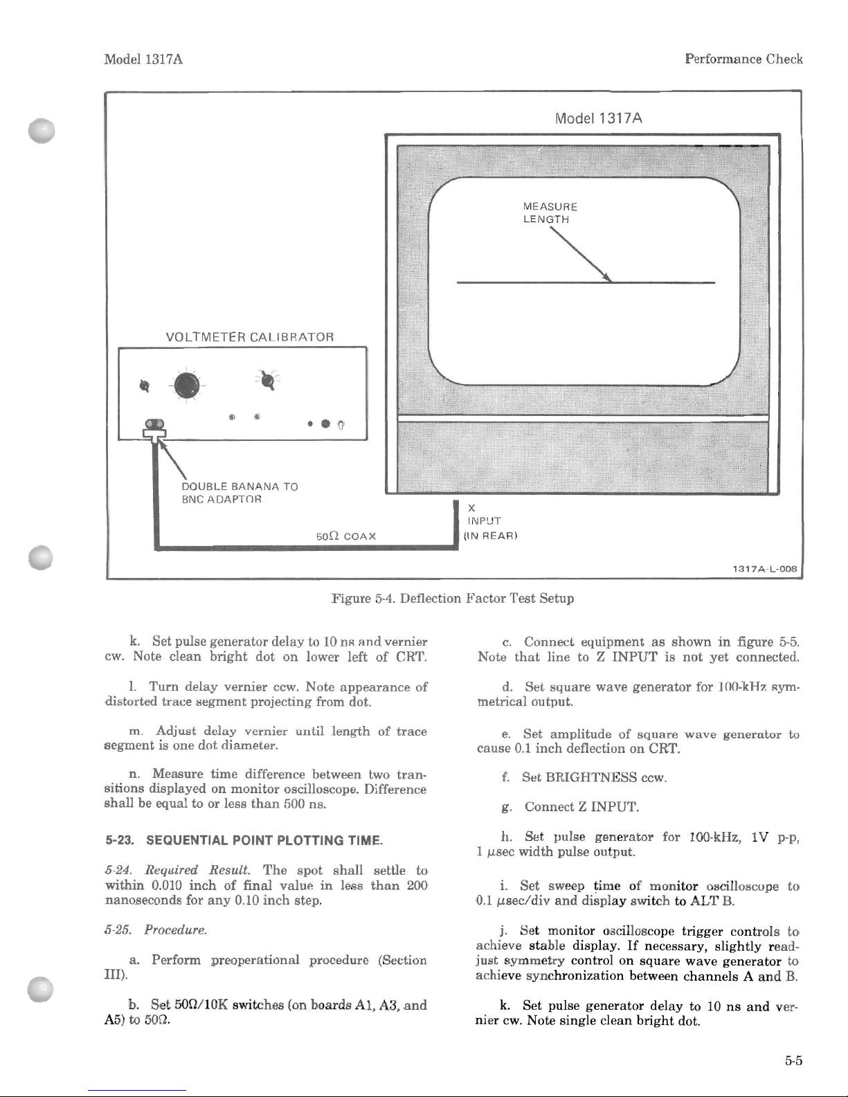
Model13l7A
VOLTMETER
CALIBRATOR
..
-*-
I
1\
@ @
DOUBLE
BANANA
TO
BNC
ADAPTOR
• •
{)l
50[2
COAX
X
INPUT
(IN
REAR)
Model 1317A
MEASURE
LENGTH
~
Performance Check
1317
A-L-008
Figure
5-4.
Deflection
Factor
Test
Setup
k.
Set
pulse
generator
delay
to
10
ns
and
vernier
cwo
Note
clean
bright
dot
on
lower left
of
CRT.
1.
Turn
delay
vernier
ccw. Note
appearance
of
distorted
trace
segment
projecting from dot.
m.
Adjust
delay
vernier
until
length
of
trace
segment
is one dot
diameter
.
n. Measure
time
difference between two
tran-
sitions displayed
on
monitor
oscilloscope. Difference
shall
be equal to
or
less
than
500
ns.
5-23. SEQUENTIAL POINT PLOTTING TIME.
5-24.
Required Result.
The
spot
shall
settle to
within
0.010
inch
of
final
value
in
less
than
200
nanoseconds for
any
0.10
inch
step.
5-25.
Procedure.
a. Perform
preoperational
procedure (Section
III).
b.
Set
500/lOK
switches (on
boards
AI,
A3,
and
A5) to 500.
c.
Connect
equipment
as
shown
in
figure
5-5.
Note
that
line to Z
INPUT
is
not
yet
connected.
d.
Set
square
wave
generator
for 100-kHz sym-
metrical output.
e.
Set
amplitude
of
square
wave
generator
to
cause
0.1
inch
deflection
on
CRT.
f.
Set
BRIGHTNESS
ccw.
g. Connect
Z
INPUT.
h.
Set
pulse
generator
for 100-kHz,
IV
p-p,
llJ.sec
width
pulse output.
i.
Set
sweep
time
of
monitor
oscilloscope
to
O.llJ.sec/div
and
display
switch
to
ALT
B.
j.
Set
monitor oscilloscope
trigger
controls
to
achieve
stable
display.
If
necessary,
slightly
read-
just
symmetry
control
on
square
wave
generator
to
achieve
synchronization
between
channels A and
B.
k.
Set
pulse
generator
delay
to 10
ns
and
ver-
nier
cwo
Note single
clean
bright
dot.
5-5
Page 26
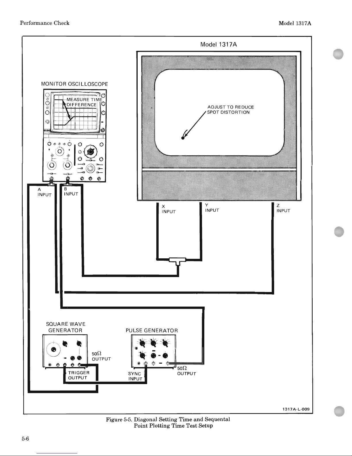
Performance Check
5-6
MONITOR
OSCI LLOSCOPE
/ 0
MEASURE
TIME
DIFFERENCE
"
A
INPUT
B
INPUT
SQUARE
WAVE
GENERATOR
I
..
_
0 1
-
..
@
~ ~
TRIGGER
OUTPUT
"
50n
OUTPUT
X
INPUT
PULSE
GENERATOR
~~.~
rt)
.i-'
Model 1317A
ADJUST
TO
REDUCE
/ SPOT
DISTORTION
Y
INPUT
~
~ -~
........
~
~--~------~50n
SYNC
OUTPUT
INPUT
Figure
5-5.
Diagonal
Setting
Time
and
Sequental
Point
Plotting
Time
Test
Setup
Model 1317A
Z
INPUT
1317
A-L-009
Page 27
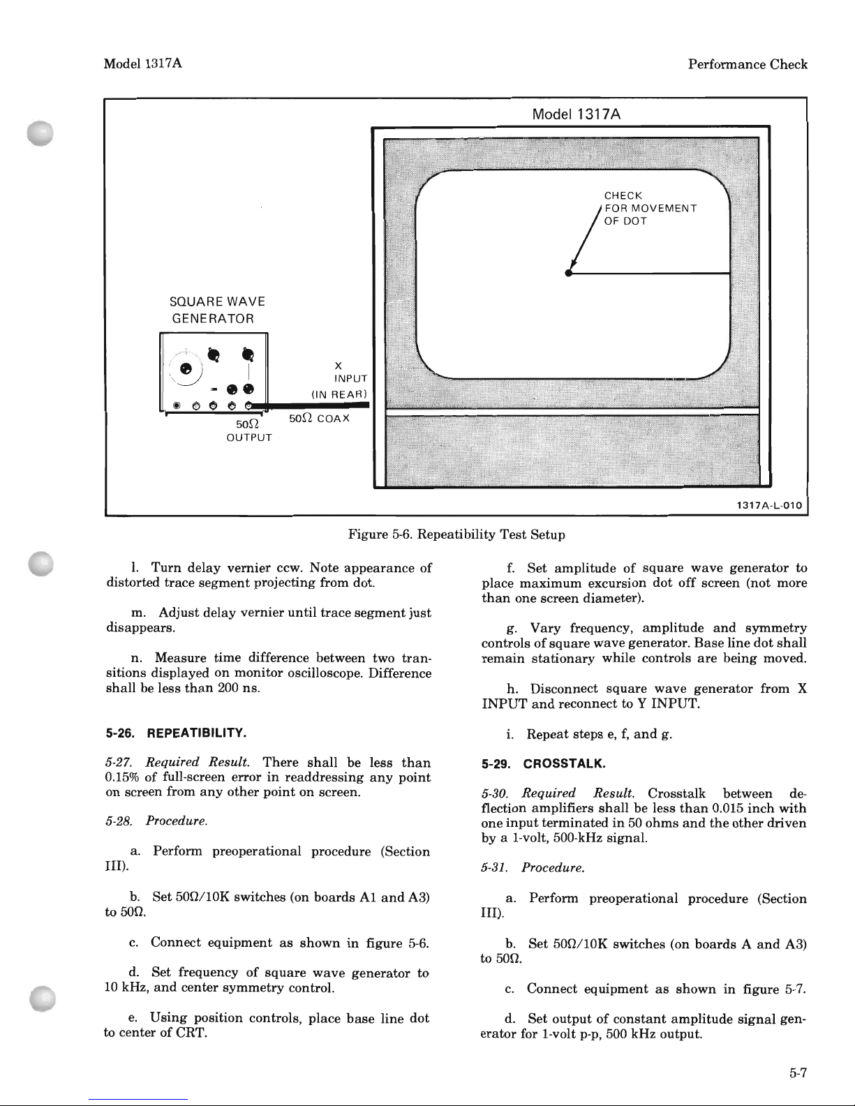
Model 1317A
SQUARE
WAVE
GENERATOR
50n
OUTPUT
X
INPUT
(IN
REAR)
50n
COAX
Performance
Check
Model 1317A
CHECK
FOR
MOVEMENT
OF
DOT
1317A-L-010
Figure
5-6.
Repeatibility
Test
Setup
1.
Turn
delay
vernier
ccw. Note
appearance
of
distorted
trace
segment
projecting from dot.
m.
Adjust
delay
vernier
until
trace
segment
just
disappears.
n. Measure time difference between two
tran-
sitions displayed
on
monitor
oscilloscope. Difference
shall
be less
than
200
ns.
5-26. REPEATIBILITY.
5-27.
Required Result.
There
shall
be less
than
0.15%
of
full-screen
error
in
readdressing
any
point
on
screen from
any
other
point
on
screen.
5-28.
Procedure.
a. Perform
preoperational
procedure (Section
III).
b.
Set
500/10K
switches (on
boards
Al
and
A3)
to
SOD.
c.
Connect
equipment
as
shown
in
figure
5-6.
d.
Set
frequency
of
square
wave
generator
to
10 kHz,
and
center
symmetry
control.
e. U sing
position controls,
place
base
line
dot
to center
of
CRT.
f.
Set
amplitude
of
square
wave
generator
to
place
maximum
excursion
dot
off
screen (not more
than
one screen diameter).
g.
Vary
frequency,
amplitude
and
symmetry
controls
of
square
wave
generator.
Base
line
dot
shall
remain
stationary
while controls
are
being
moved.
h. Disconnect
square
wave
generator
from X
INPUT
and
reconnect to Y
INPUT.
i.
Repeat
steps
e,
f,
and
g.
5-29. CROSSTALK.
5-30.
Required Result.
Crosstalk
between de-
flection amplifiers
shall
be less
than
0.015
inch
with
one
input
terminated
in
50
ohms
and
the
other
driven
by
a I-volt, 500-kHz signal.
5-31.
Procedure.
a. Perform preoperational procedure (Section
III).
b.
Set
500/10K
switches (on
boards A and
A3)
to
soo.
c.
Connect
equipment
as
shown
in
figure
5-7.
d.
Set
output
of
constant
amplitude
signal
gen-
erator
for I-volt p-p, 500 kHz output.
5-7
Page 28
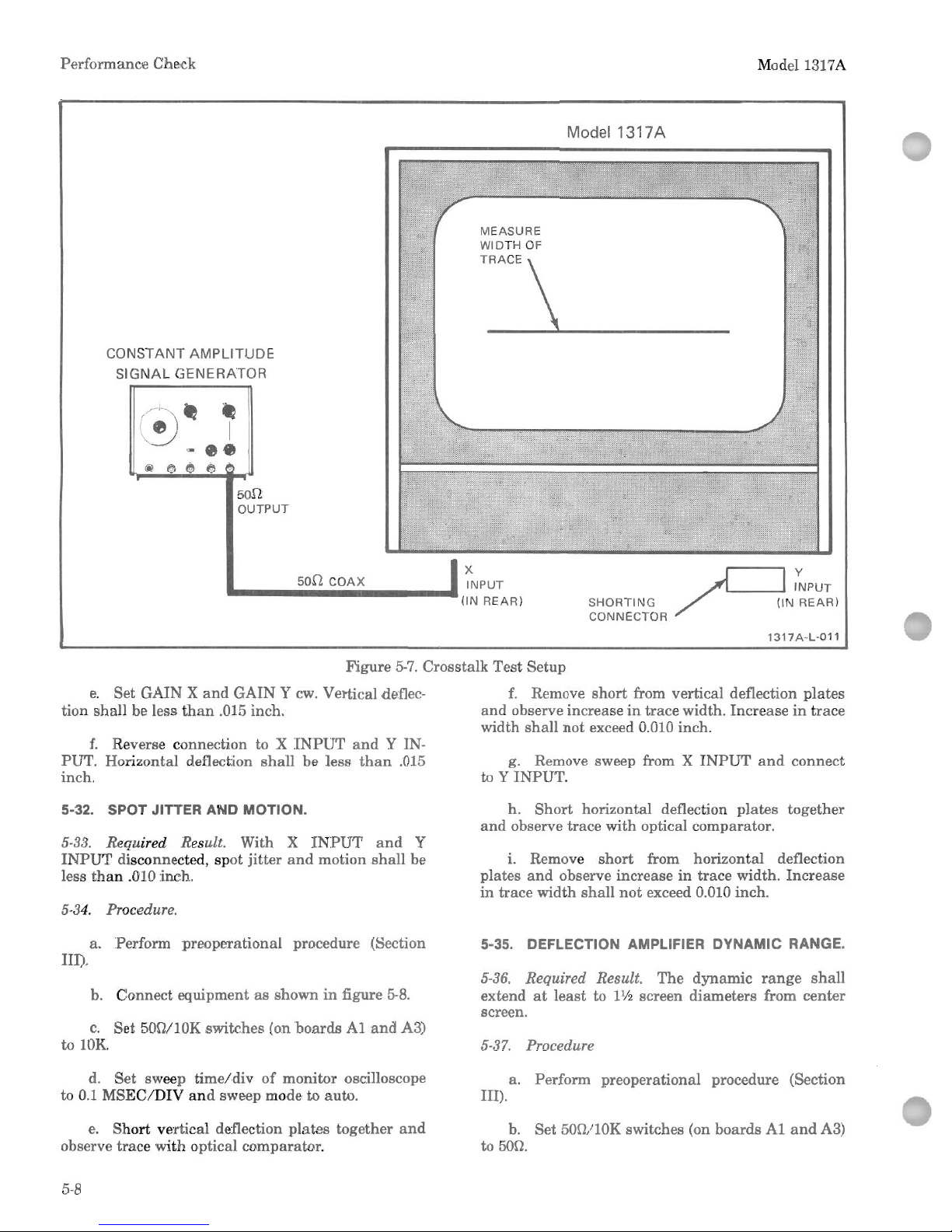
Performance
Check
CONSTANT
AMPLITUDE
SIGNAL
GENERATOR
I _ •
01
coo
••
@
@)
~
~
50Q
OUTPUT
MEASURE
WIDTH
OF
TRACE
\
Model 1317A
Model 1317A
50Q
COAX
INPUT
..
-----------
..
ON
REAR)
SHORTING
A
__
~
CONNECTOR
/'
1317A-L-011
Figure
5-7.
Crosstalk
Test
Setup
e.
Set
GAIN X and
GAIN Y cwo
Vertical deflec-
f.
Remove
short
from vertical deflection
plates
tion
shall
be less
than
.015 inch.
and
observe
increase
in
trace
width.
Increase
in
trace
width
shall
not
exceed 0.010 inch.
f.
Reverse connection to X
INPUT
and
Y IN-
PUT.
Horizontal deflection
shall
be less
than
.015
inch.
5-32. SPOT JITTER AND MOTION.
5-33.
Required Result. With X
INPUT
and
Y
INPUT
disconnected,
spot
jitter
and
motion
shall
be
less
than
.010 inch.
5-34.
Procedure.
a. Perform
preoperational
procedure (Section
III).
b. Connect
equipment
as
shown
in
figure
5-8.
c.
Set
500/10K
switches (on
boards
Al
and
A3)
to 10K.
d.
Set
sweep
time/div
of
monitor
oscilloscope
to 0.1
MSEC/DIV
and
sweep mode to auto.
e.
Short
vertical deflection
plates
together
and
observe
trace
with
optical
comparator.
5-8
g.
Remove sweep from X
INPUT
and
connect
to Y
INPUT.
h.
Short
horizontal
deflection
plates
together
and
observe
trace
with
optical
comparator.
i.
Remove
short
from
horizontal
deflection
plates
and
observe
increase
in
trace
width.
Increase
in
trace
width
shall
not
exceed 0.010 inch.
5-35. DEFLECTION AMPLIFIER DYNAMIC RANGE.
5-36.
Required Result.
The
dynamic
range
shall
extend
at
least
to 11
/2
screen
diameters
from
center
screen.
5-37.
Procedure
a.
Perform
preoperational
procedure (Section
III).
b.
Set
50n/10K
switches (on
boards
Al
and
A3)
to 500.
Page 29
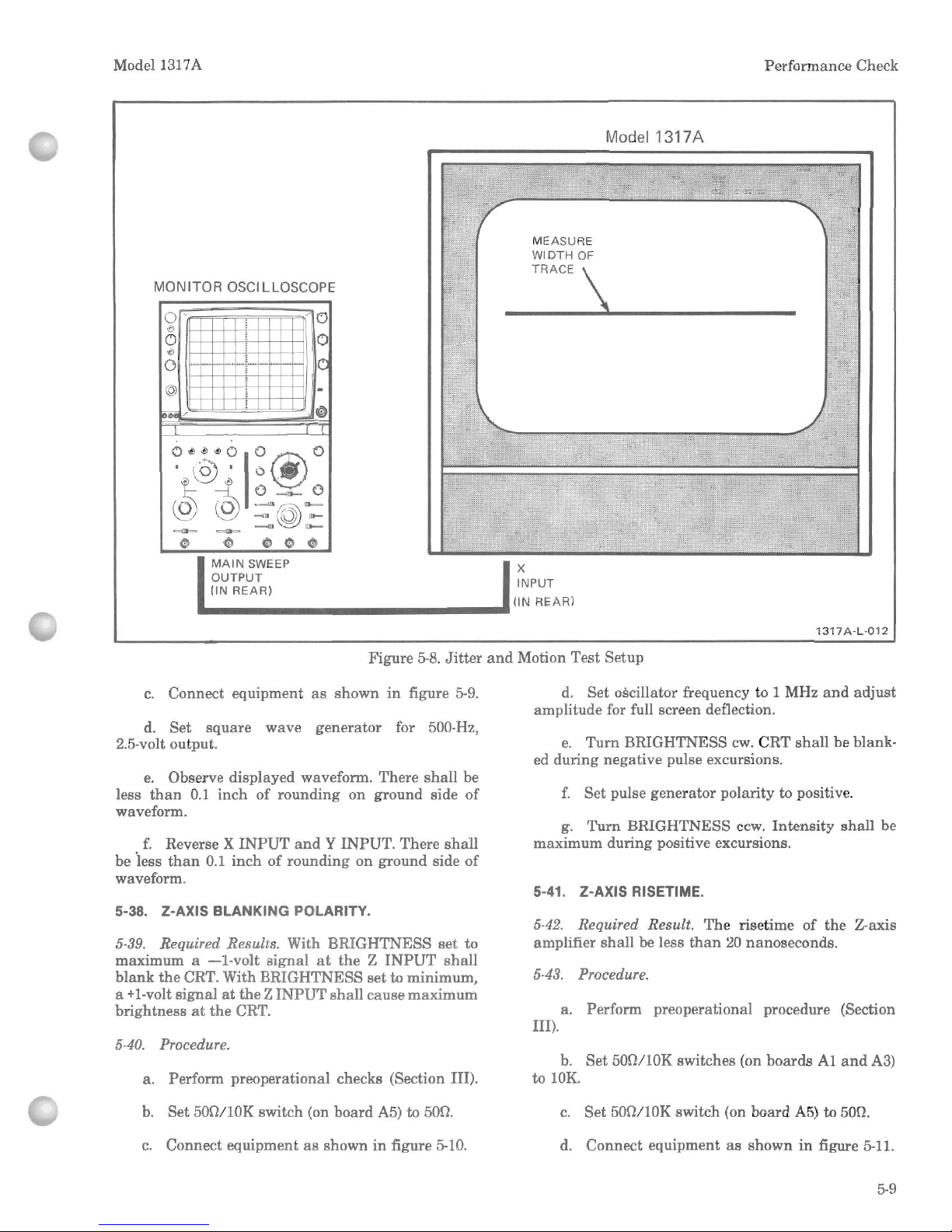
Model 1317A
MONITOR OSCILLOSCOPE
o '
/ 0
@
()
0
®
0
10
@
-
ftH
/
@)
I
I
O~HOIO@O
·
@.
0
J_
@~
0=0=0
o
@:::(Q):::
=-=
=0=
~
~
0
0
MAIN
SWEEP
OUTPUT
(IN
REAR)
~
MEASURE
WIDTH
OF
Model 1317A
TRACE
\
X
INPUT
Performance Check
..................................
(lNREAR)
1317
A-L-012
Figure
5-8.
Jitter
and
Motion
Test
Setup
c.
Connect
equipment
as
shown
in
figure
5-9.
d.
Set
square
wave
generator
for 500-Hz,
2.5-volt output.
e.
Observe displayed waveform.
There
shall
be
less
than
0.1
inch
of
rounding
on
ground
side
of
waveform.
f.
Reverse X
INPUT
and Y INPUT.
There
shall
be
iess
than
0.1
inch
of
rounding
on
ground
side
of
waveform.
5-38. Z-AXIS BLANKING POLARITY.
5-39.
Required Results. With
BRIGHTNESS
set
to
maximum a -I-volt
signal
at
the Z INPUT
shall
blank
the
CRT. With
BRIGHTNESS
set
to
minimum,
a +l-volt
signal
at
the Z INPUT
shall
cause
maximum
brightness
at
the
CRT.
5-40.
Procedure.
a. Perform
preoperational
checks (Section III).
b.
Set
500/10K
switch
(on
board
A5) to 50n.
c.
Connect
equipment
as
shown
in
figure 5-10.
d.
Set
oscillator frequency to 1 MHz
and
adjust
amplitude for full screen deflection.
e.
Turn
BRIGHTNESS
cwo
CRT
shall
be blank-
ed
during
negative
pulse excursions.
f.
Set
pulse
generator
polarity
to positive.
g.
Turn
BRIGHTNESS
ccw.
Intensity
shall
be
maximum
during
positive excursions.
5-41. Z-AXIS RISETIME.
5-42.
Required Result.
The
risetime
of
the
Z-axis
amplifier
shall
be less
than
20
nanoseconds.
5-43.
Procedure.
a.
Perform
preoperational procedure (Section
III).
b.
Set
500/10K
switches (on
boards
Al
and
A3)
to
10K.
c.
Set
500/10K
switch
(on
board
A5) to 50n.
d.
Connect
equipment
as
shown
in
figure 5-11.
5-9
Page 30

Performance
Check
Model1317A
Model 1317A
SQUARE
WAVE
GENERATOR
IRIGGER
OUTPUT
50n
OUTPUT
y
INPUT
(IN R
EAR)
MEASURE
VERTICAL
HEIGHT
OF
ROUNDING
X
INPUT
(IN
REAR)
MAIN
SWEEP
OUTPUT
(IN
REAR)
MONITOR
OSCILLOSCOPE
0'
@
0
IS>
0
@
Ioii /
I
VERTICAL
INPUT
/
C)
"
10
-
.:..18
I I
1317
A -
L-013
Figure 5-9.
Dynamic
Range
Test
Setup
e.
Set
oscillator frequency to I MHz and
ampli
-
tude
to
display
full screen
raster
on
CRT.
f.
Set
square
wave
generator
for 100-kHz,
50-volt
output
at
A5TPl.
5-10
g.
Set
monitor
oscilloscope to observe
leading
edge
of
displayed
waveform
with
display
exactly
filling
vertical
graticule.
h.
Observe risetime between
vertical
10%
and
90%
points. Risetime
shall
be
less
than
20
ns.
Page 31

Model 1317A
PULSE
GENERATOR
~
~
••
(j)
.i-it
@
~
-
~
TRIGGER
OUTPUT
OSCILLAROR
" -.:
c~
@ @
PULSE
OUTPUT
• •
C(j)
X
INPUT
(IN
REAR)
50n
COAX
Z
INPUT
(IN
REAR)
Performance Check
MONITOR
OSCI
LLOSCOPE
o '
/ 0
@
()
0
®
0
0
@
-
OH
/
;J"
I
~
. .
o
I.!!
:lJ,1!l C) I 0
Ilt\
0
MAIN
SWEEP
· @ .
~
OUTPUT
,
~
~
c =-= C
~EAR)
(Q)
\QJ
~
::
......0
_
TRIGGER
INPUT
Model 1317A
CHECK
FOR
Y
INPUT
(IN
REAR)
MAXIMUM
INTENSITY
OR
BLANKED
SEGMENTS
1317
A -
L-014
Figure
5-10.
Blanking
Polarity
Test
Setup
5-11
Page 32

Performance
Check
Model 1317A
5-12
SQUARE
WAVE
GENERATOR
TRIGGER
OUTPUT
50n
OUTPUT
MONITOR
OSCILLOSCOPE
0'
/
CJ
@
I
H--+-+-+-+--~
"""-I
C) - - - - - -
~
.-
0l...--
MEASURE
I§!
!/
....
Iooo
It-,
RISETIME
o v
@ - -
-y
Oiij
/
@)
MAIN
SWEEP
I I I
OUTPUT
o@o
o~
O.
@:tJ'\!)01
0
!It\
0 (IN
REAR)
k
~
C~C
@ \9)
=:©):=
~
=-=
~
0
~
0
VERTICAL
TRIGGER
INPUT
INPUT
~
I , 10:1
DIVIDER
PROBE
.-----------
...
Z
CONNECTED
TO
A5TP1
50H
COAX
I
INPUT
RASTER
DISPLAY
TO
PREVENT
BURNING
OSCILLATOR
(IN
REAR)
Model 1317A
-
._*
-
'I
\
@ @
o .
• •
{)l
Y
INPUT
(IN
REAR)
Figure
5-11. Z-axis Risetime
Test
Setup
X
INPUT
(IN
REAR)
1317A-L-015
Page 33

Model 1317A
PERFORMANCE
CHECK RECORD
MODEL
1317A
Instrument
Serial
Number
_____
_
Check
Specification
DEFLECTION AMPLIFIER RISETIME
X
Amplifier
~75
ns
Y
Amplifier
~75
ns
DEFLECTION AMPLIFIER BANDWIDTH
X
Amplifier
~
3.7 inches
Y
Amplifier
~
3.7 inches
DEFLECTION AMPLIFIER PHASE
SHIFT
50 kHz
<0.1°
250 kHz
<1°
DEFLECTION FACTOR
X
minimum
~
5.6 inches
X maximum
10 inches ±3%
Y
minimum
~
5.6 inches
Y maximum
10 inches ±3%
DIAGONAL SETTLING
TIME
<500
ns
SEQUENTIAL POINT PLOTTING
TIME
<200
ns
REPEATIBI
LlTY
<0.15%
CROSSTALK
<0.015
inch
SPOT
JITTER AND MOTION
<0.010
inch
DEFLECTION AMPLIFIER
DYNAMIC
RANGE
X
Amplifier
<0.1
inch
Y
Amplifier
<0.1
inch
Performance
Check
Date
_______
_
Measured
5-12a
Page 34

Performance
Check
Check
PERFORMANCE CHECK RECORD
MODEL 1317A (Cont'd)
Instrument Serial Number
____
_
Specification
Z-AXIS
BLANKING POLARITY
per
text
Z-AXIS
RISETIME
<20
ns
5-12h
Model 1317A
Date
_______
_
Measured
Page 35

Model 1317A
5-44. ADJUSTMENTS.
WARNING I
Do
not
attempt
to
operate
this
instru-
ment
until
the
safety
summary,
located
just
before Section I,
has
been
read
and
understood.
5-45.
The
following
paragraphs
describe procedures
to
calibrate
the
instrument
so
that
it
will perform
as
specified
in
Section
I.
For
complete
calibration,
the
entire
procedure
should
be
performed
in
sequence;
individual
adjustments
can
be
made
by
following
the
steps
in
the
appropriate
paragraphs.
Adjustment
controls
are
shown
on
a fold-out
illustration
at
the
end
of
this
section.
5-46. Remove
top
and
bottom
covers before con-
necting
instrument
for operation.
Turn
instrument
on
and
allow
1/2
hour
warm-up
time.
Use
a non-
metallic screwdriver
and
recently
calibrated
test
equipment
with
characteristics
as
specified
i~
table
5-1.
After
adjustments
are
completed, check Instru-
ment
performance
by
accomplishing
the
performance
checks described earlier
in
this
section.
5-47. LOW VOLTAGE POWER SUPPLY ADJUSTMENTS.
5-48.
References.
Schematic
10,
table
5-1,
and
figure
5-16.
5-49.
Procedure.
a.
Connect
digital
voltmeter
to
red
lead
on
low
voltage power
supply
board
All.
b.
Set
+250
ADJ
A11R12 for
reading
of
exactly
+250
volts on
digital
voltmeter.
c.
Alternately
connect
digital
voltmeter
to
violet lead
and
white/red
lead
on
low
voltage
power
supply
board
All.
d.
Set
±15
ADJ
A11R29
to
divide
any
error
equally between
the
outputs.
Final
error
on
either
output
must
be
±0.1
volts
or
less.
5-50. HIGH VOLTAGE POWER SUPPLY ADJUSTMENT.
WARNING I
Contact
with
high
voltages
in
this
instru-
ment
can
cause
injury
or
death.
5-51.
References.
Schematic
7,
schematic
11,
table
5-1,
and
figure 5-16.
Adjustments
5-52.
Procedure.
a. Monitor +250-volt
supply
using
1000:1 divi-
der probe
and
digital
voltmeter.
b. Multiply voltage
reading
from
step a by
-18.
c.
Monitor
output
of
high
voltage
power
supply
at
HV
test
point
on
z-axis
board
A5.
d.
Set
HIGH
VOLTAGE
ADJ
A13R2
to
obtain
voltage
reading
equal
to
result
in
step
b.
5-53. TRACE ALIGN AND ORTHOGONALITY ADJUSTMENTS.
5-54.
References.
Schematic
11,
table
5-1,
and
figure 5-16.
5-55.
Procedure.
a.
Perform
preoperational
procedure (Section
III).
b.
Set
5Q{2I10K
switches
(on
boards
Al
and
A3)
to 10K.
c.
Apply
I-volt p-p
signal
from
voltmeter
cali-
brator
to X
INPUT.
d.
Set
TRACE
ALIGN
A9R4 to
cause
trace
to lie
along x axis
of
CRT. Because
the
CRT
has
no
grati-
cule, some
external
means
should
be devised
to
accurately
locate x axis.
e.
Disconnect voltmeter
calibrator
from X IN-
PUT
and
connect to Y
INPUT.
f.
Set
ORTHOG A9R9 to
cause
trace
to lie per-
pendicular
to x
axis
(along
y axis). Because
the
CRT
has
no graticule, some
external
means
should
be
devised to
accurately
locate y axis.
5-56.
Z-AXIS
ADJUSTMENTS.
5-57.
References.
Schematic
7,
schematic
11,
table
5-1,
and
figures 5-12
and
5-16.
5-58.
Procedure.
a.
In
adjusting
Z-axis
gain
and
balance,
monitor
voltage on
the
wiper
arm
of
Z-axis
balance
adjust-
ment
A5R65
and
adjust
for zero volts
±10 m V.
b. Apply
-1
volt
into
Z-input
and
adjust
Z-axis
gain
A5R20
until
spot
is
just
extinguished.
c.
Perform
preoperational
procedure (Section
III).
d.
Set
500/10K
switches
(on
boards
Al
and
A3)
to 10K.
e.
Set
500/10K
switch
(on
board
A5) to
50f2.
5-13
Page 36

Adjustments
Model 1317A
SQUARE
WAVE
GENERATOR
I
__
0 1
~
..
@ ®
~
TRIGGER
OUTPUT
50n
OUTPUT
MONITOR
OSCILLOSCOPE
ADJUST
OVERSHOOT
~r;~~~~~~~~'
___
ADJUST
leo'
.-
/
.1ZS-
~
.1JlIr,
!.~~ - .
FLAT
TOP
o - - - -II \
~~
0
CHECK
~
I
",I----
RISETIME
o I \ - v
@ -
i.J/
I-
- - - I
\,
!eM '"
@)
MAIN
SWEEP
I I
OUTPUT
. .
<:>
~.olJ
<iJ
0 I 0 .Ilt\ 0 I (IN
REAR)
·
@.
o\!;
.
~
~
C
--=
0
@
\QJ
=:©)=
<=0=
=C»=>
~.
~
@)
.)
0
VERTICAL
TRIGGER
INPUT
INPUT
~
I \ 10:1
DIVIDER
PROBE
.-----------_
Z
CONNECTED
TO
A5TP1
50H
COAX
I
INPUT
RASTE R
DISPLAY
TO
PREVENT
BURNING
OSCILLATOR
(IN
REAR)
Model 1317A
X
INPUT
(IN
REAR)
" .-
, I
0. .
@ @
• •
!OJ
1317
A-L-016
Figure
5-12.
Equipment
Setup for Z-axis
Adjustments
5-14
Page 37

Model 1317A
f.
Connect
digital
voltmeter between
A5TPI
and
chassis
ground.
g. Set
BRIGHTNESS
for + 10V
reading
on
digital
voltmeter.
h.
Set
INTS
LIMIT
A13R16 to
barely
extinguish
a
sharply
focussed spot.
1.
Connect
equipment
as
shown
in
figure 5-12.
j.
Set
oscillator frequency to 1 MHz
and
amplitude
for full screen display.
k.
Apply
500
output
of
square
wave
generator
to
Z
INPUT.
1.
Connect
monitor
oscilloscope to
A5TPl.
m.
Set
vertical
input
coupling
of
monitor
oscillo-
scope to dc.
n.
Set
monitor
oscilloscope controls to view
one square-wave period
at
A5TP1.
o.
Set
square
wave
generator
controls for 100-
kHz, 50-volt
output
at
A5TPl.
p.
Set
BRIGHTNESS
so
that
waveform
at
A5TPI
does
not
limit.
q.
Set
monitor
oscilloscope controls so
that
waveform
just
fills vertical graticule.
r.
Set
HF
ADJ
NO. 1 A5C12 for
small
amount
of
overshoot (less
than
1%)
on
leading
edge positive
response.
s.
Set
HF
ADJ
NO. 2 A5R37 for
flattest
res-
ponse
after
leading
edge
transition.
t.
Observe risetime.
It
shall
be less
than
20
ns.
u.
If
risetime fails to
meet
specification,
repeat
step
q,
slightly
increasing
overshoot.
v.
Repeat
steps s, t,
and u until
risetime specifi-
cation
is
met
with
minimum
overshoot.
Overshoot
must
not
be
increased
to
point
where
amplifier
tends
to oscillate,
and
in
no
case,
should
it
exceed 5%.
5-59. HORIZONTAL AMPLIFIER LOW FREQUENCY
ADJUSTMENTS.
5-60.
References.
Schematic
1,
schematic
2,
schematic
3,
table
5-1,
and
figure 5-16.
5-61.
Procedure.
a. Remove
ground
strap
from
digital
voltmeter
and
connect differentially
to
horizontal
deflection
plates
(neck
pins
on
CRT).
Adjustments
b.
Set
POSITION
X for
OV
reading
on
digital
voltmeter.
c.
Disconnect
digital
voltmeter
common
lead
and
connect to
chassis
ground.
d.
Set
AVERAGE
A1R64 for +108V
reading
on
digital voltmeter.
e.
Disconnect digital voltmeter. Replace
ground
strap.
f.
Turn
GAIN X back
and
forth
between
its
cw
and
ccw positions while
observing
spot
on
CRT.
Set
BAL A1R11 to minimize
movement
of
spot.
Spot
movement
shall
not
exceed 0.3 inch.
g.
Set
500/10K
switch
(on
board
A5) to 10K.
h. Apply 400 Hz,
IV
p-p
signal
from voltmeter
calibrator
to X
INPUT.
1.
Set
GAIN X cwo
j.
Set
GAIN
A1R12 for 10
inches
deflection
on
CRT.
5-62. VERTICAL AMPLIFIER LOW FREQUENCY
ADJUSTMENTS.
5-63. References.
Schematic
4,
schematic
5,
schematic
6,
table
5-1,
and
figure 5-16.
5-64.
Procedure.
a. Remove
ground
strap
from
digital
voltmeter
and
connect differentially to vertical deflection
plates
(neck
pins
on CRT).
b.
Set
POSITION
Y for
OV
reading
on
digital
voltmeter.
c.
Disconnect
digital
voltmeter
common
lead
and
connect to
chassis
ground.
d.
Set
AVERAGE
A3R64 for + 108V
reading
on
digital
voltmeter.
e.
Disconnect
digital
voltmeter. Replaced
strap.
f.
Turn
GAIN Y back
and
forth
between
its
cw
and
ccw positions while
observing
spot
on
CRT.
Set
BAL
A3Rll
to minimize
movement
of
spot.
Spot
movement
shall
not
exceed 0.3 inch.
g.
Set
500/10K
switch
(on
board
A3) to 10K.
h. Apply 400 Hz,
IV
p-p
signal
from
voltmeter
calibrator
to Y
INPUT.
i.
Set
GAIN Y cwo
5-15
Page 38

Adjustments
j.
Set
GAIN
A3R12 for 10
inches
deflection
on
CRT.
5-65. HORIZONTAL AMPLIFIER RESPONSE ADJUSTMENTS.
5-66.
References.
Schematic
1,
schematic
2,
schematic
3,
table
5-1,
figure 5-13,
and
figure 5-16.
5-67. Procedure.
a.
Perform
preoperational
procedure (Section
III).
b.
Set
500/10K
switches
(on
boards
Al
and
A3)
to 500.
c.
Connect
equipment
as
shown
in
figure 5-13.
d.
Set
square
wave
generator
contro
ls for 10
kHz,
maximum
amplitude
output
signal.
e.
Center
display
with
POSITION X and
POSI-
TION
Y.
f.
Set
monitor
oscilloscope controls for stable,
full-screen
display
of
two
square-wave
periods.
g.
Set
LF
ADJ
NO. 1 A2R24,
and
LF
ADJ
NO.
2 A2C17 for
flattest
pulse
response
on
ground
side
of
display.
h. Disconnect
square
wave
generator
from X
INPUT
and
connect
constant
amplitude
signal
gen-
erator.
i.
Set
frequency
of
constant
amplitude
signal
generator
to 50 kHz
and
amplitude
to
cause 5 inches
deflection
on
CRT
.
j.
Change
frequency
of
constant
amplitude
signal generator
to 5 MHz.
k.
Set
HF
ADJ
NO. 1 A2C8
and
HF
ADJ
NO.2
A2C
12
for vertical deflection
of
3.7 inches.
5-68. VERTICAL AMPLIFIER RESPONSE ADJUSTMENTs.
5-69.
References.
Schematic
4,
schematic
5,
schematic
6,
table
5-1
, figure 5-14,
and
figure 5-16.
5-70
. Procedure.
a.
Perform
preoperational
procedure (Section
III)
.
b.
Set
500 / 10K
switches
(on
boards
Al
and
A3)
to 500.
c.
Connect
equipment
as
shown
in
figure 5-14.
5-
16
Model 1317A
d.
Set
square
wave
generator
controls
for 10
kHz,
maximum
amplitude
output
signal.
e.
Center
display
with
POSITION X and
POSI-
TION
Y.
f.
Set
monitor
oscilloscope for stable, full-
screen
display
of
two square-wave periods.
g.
Set
LF
ADJ
NO.1
A4R24
and
LF
ADJ
NO.2
A4C17 for
flattest
pulse
response
on
ground
side
of
di
splay.
h. Disconnect
square
wave
generator
from Y
INPUT
and
connect
constant
amplitude
signal
gener-
ator.
i.
Set
frequency
of
constant
amplitude
signal
generator
to 50 kHz
and
amplitude
to
cause 5 inches
of
deflection on CRT.
j.
Change
frequency
of
constant
amplitude
signal
generator
to 5 MHz.
k.
Set
HF
ADJ
NO.1
A4C8
and
HF
ADJ.
No.2
A4C12 for vertical deflection
of
3.7
inches
.
5-71. PHASE SHIFT ADJUSTMENT.
5-72. References.
Schematic
3,
schematic
6,
table
5-1, figure
5-15
and
figure 5-16.
5-73.
Procedure.
a.
Perform
preoperational
procedure (Section
III).
b. Set
500/10K
switches
(on
boards
Al
and
A3)
to 500.
c.
Connect
equipment
as
shown
in
figure 5-15.
d.
Set
frequency
of
constant
amplitude
signal
ge
nerator
to 250 kHz
and
amplitude
for full-screen
diagonal
line (or ellipse)
on
CRT.
e.
If
separation
of
ellipse
at
center
of
display
is
greater
than
0.1
inch,
make
small
adjustments
to
A2C8, A2C12, A4C8,
and
A4C12
until
ellipse
separa-
tion is less
than
0.1
inch.
Note
The
procedures
in
step
d above,
in
para
-
graph
5-70
step
n,
and
in
paragraph
5-67
step n are
interactive.
Repeat
these
pro-
cedures
until
the
requirements
of
all
three
are
satisfied.
Page 39

Model 1317A
FOR BW
ADJUST
SQUARE WAVE
GENERATOR
~
-
-
~
I
@
@)
TRIGGER
OUTPUT
....
e
50n
OUTPUT
X
INPUT
(IN
REAR)
..
________
50n
COAX
Model 1317A
y
INPUT
(IN
REAR)
Adjustments
MONITOR
OSCI
LLOSCOPE
MAIN
SWEEP
OUTPUT
(IN
REAR)
0
~
0l
n I
0
II I I
®
I I !
0
I
@
i
I
8M
;'
I
/
0
I I "
~
I
0
i
I
10
i I
I
I -
I II
. \i)
1 I
VERTICAL
..
________________________
..
INPUT
CONSTANT
AMPLITUDE
SIGNAL
GENERATOR
50n
OUTPUT
50n
COAX
Figure
5-13
. Equipment Setup for Horizontal Amplifier · Response Adjustments
1317
A-L-017
5-17
Page 40

Adjustments
Model 1317A
MODEL
1317A
DISPLAY
FOR BW
ADJUST
X
I
NPUT
(IN
REAR)
Model 1317A
Y
INPUT
(IN
REAR)
MONITOR OSCILLOSCOPE
SQUARE
WAVE
GENERATOR
TRIGGER
OUTPUT
.
50n
OUTPUT
..
_______
50rl
COAX
MAIN
SWEEP
OUTPUT
(IN
REAR)
o '
@
0
@
0
@
eiMi /
I
VERTICAL
....................................................
INPUT
/ 0
"
0
-
~
I I
CONSTANT
AMPLITUDE
SIGNAL
GENERATOR
5-18
50rl
OUTPUT
50n
COAX
Figure
5-14.
Equipment
Setup
for Vertical Amplifier
R~sponse
Adjustments
1317
A -
L-018
Page 41

Model 1317A
5-74. FOCUS AND ASTIGMATISM ADJUSTMENTS.
WARNING.
Contact
with
high
voltages
in
this
instru-
ment
can
cause
injury
or
death.
5-75. References.
Schematics
7,
8,
9,
and
11.
Tables
5-1
and
5-2.
Figures
5-16, 5-17,
and
5-18.
5-76. Procedure.
a. Set
BRIGHTNESS
for dim
spot
on CRT.
b.
Center
spot
with
POSITION X and
POSI-
TION
Y.
c.
Connect
digital
voltmeter
between
A6RI08
1
A6R
11
0 junction
and
ground.
d.
Set
FOCUS
for + 10V
reading
on
digital
volt-
meter.
e.
Set
ASTIG
and
FOCUS
LIMIT
A12R6 for
smallest,
most
round
spot.
f.
Disconnect
digital
voltmeter.
g.
Set
FY1A6R10, FY2A6R11, FX1A6R23,
FX2A6R24, AY1A6R61, AY2A6R62, AX1A6R74,
AX2A6R75,
and
DRIVE
FOCUSING
ADJUST
A6R43
ccw.
h.
Center
FOCUS
and
ASTIG.
i.
Adjust F BAL
A6R44
and A BAL
A6R90 for
best
focused spot.
j.
Use
felt
tip
pen
to
mark
face
of
CRT
as
shown
in
figure 5-17.
k.
Position
spot
to
point
1.
1.
Set
FOCUS
and
ASTIG
for
smallest,
best-
defined spot.
m. Position
spot
to
point
2.
n.
Set
FXIA6R23
and
AX1A6R74 for
smallest,
best-defined spot.
o.
Repeat
steps m and
n for
each
point
listed
in
table
5-2.
Adjustments
p.
Center
FOCUS
and
ASTIG.
q.
Connect
equipment
as
shown
in
figure 5-18.
r.
Set
pulse
generator
for positive-going, 0.5
usec wide,
20
kHz,
IV
p-p output.
s. Adjust F BAL A6R44 to
set
most
negative
ex-
cursion,
as
displayed on
monitor
oscilloscope, to
+5V.
t.
Readjust
ASTIG
and
FOCUS
LIMIT
A12R6
for best-defined spot.
u. Disconnect pulse
generator
from Z
INPUT.
v.
Adjust
GAIN
A6R43 for focused spot.
w.
Repeat
steps s through v several
times;
alternating
between
bright
spot
(pulse
generator
con-
nected to Z
INPUT)
and
dim
spot
(pulse
generator
disconnected)
until
best
compromise between two
conditions is reached.
x.
Connect
1kHz
sine
wave
from
constant
amplitude
signal
generator
to
both X and Y INPUT.
y.
Set
amplitude
to
cause a diagonal
line
display
from corner to corner on CRT.
z.
Connect
pulse
generator
to Z
INPUT.
Note
that
pulse (as displayed on
monitor
oscilloscope)
does
not
limit
at
top or bottom.
aa.
If
limiting
occurs
in
step
3,
readjust F BAL
A6R44
until
the
waveform does
not
limit;
then
re-
adjust
FOCUS
LIMIT
A12R6 for
best
defined spot.
5-77. FOCUS RESPONSE ADJUSTMENT.
5-78. References.
Table
5-1,
figures 5-16, 5-18,
and
schematic
7.
5-79. Procedure.
a.
Connect
equipment
as
shown
in
figure 5-18.
b.
Set
pulse
generator
for positive-going, 0.5
usec wide,
20
kHz,
IV
p-p pulse output.
c.
Synchronize
monitor
oscilloscope to negative-
going edge
of
pulse.
d. Set
HF
ADJ
NO.1
A5C12
and
HF
ADJNO.
2
A5R37 for
fastest
transition
with
less
than
5%
over-
shoot.
5-19
Page 42

Adjustments
CONSTANT
AMPLITUDE
SIGNAL
GENERATOR
50nCOAX
50n
OUTPUT
9"
COAX
Model 1317A
Figure
5-15.
Equipment
Set
up
for
Phase
Shift
Adjustment
Table
5-2.
Focus
and
Astigmatism
Adjustments
Po
int
Adjust
3
A6R24 (FX2)
A6R75 (AX2)
4
A6RI0
(FYI)
A6R61 (AYl)
5
A6Rll
(FY2)
A6R62 (AY2)
5-20
9"
COAX
BNC TEE
Model 1317A
y
INPUT
(IN
REAR)
1317
A -
L-019
Page 43

AXl
A6R74
FY2
A6R11
FX2
A6R24
--~
FX1
A6R23
HF ADJ 1
A6C4
HF ADJ 2
A6R47
X-AXIS
50n/l0Kn
SELECTOR
(UNDER COVER)
HF
AY1
A1R64
ADJ2
A6R61
AVERAGE
A2C12
HF
ADJ 1
A4C8
Y-AXIS
50n/10Kn
SELECTOR
(UNDER COVER)
AVERAGE
A3R64
Z-AXIS
50n/1
OKn
SELECTOR
PHOSPHOR PROTECTION
N/OFF
FOCUS
LIMIT
A12R6
•
1
~
___
.Jt
·
•
HV
ADJ
A13R2
•
,
.
~
•
Adjustments
250
ADJ
Al1R12
.
!-R-ri-----
±
15
ADJ
A
11
R29
1317 A-P-005-07-76
Figure
5-16.
Adjustments
Locator
5-21
Page 44

A
DISTANCE
][~f
0
.
~
0
1 2
'}
CENTER
CRT
4
o-
------+-S
--+
DIST
~NCE
5
"2
1317A
-L -
020
Figure 5-17.
CRT
Face
Marking
for Focus
and
Astigmatism
Adjustments
Adjustments
MONITOR
OSCI LLOSCOPE
PULSE
GENERATOR
-
I
••
5-22
SET
FOR
+5V
PULSE
OUTPUT
50nCOAX
ZINPUT
(REAR)
Model 1317 A
BEST
DEFINED
DOT
Figure 5-18.
Equipment
Setup
for Focus
Adjustments
Model 1317A
1317 A-L-021-08-76
Page 45

Model 1317A
Replaceable
Parts
SECTION
VI
REPLACEABLE PARTS
6-1. INTRODUCTION.
6-2.
This
section
contains
information
for ordering
replacement parts.
The
abbreviations
used
in
the
parts
list
are
described
in
table
6-1.
Table
6-2
lists
the
parts
in
alphanumeric
order
by
reference des-
ignator
and
includes
the
manufacturer
and
manu-
facturer's
part
number.
Table
6-3
contains
the
list
of
manufacturers'
codes.
6-3. ORDERING INFORMATION.
6-4.
To
obtain
replacement
parts
from Hewlett-Pack-
ard, address order or inquiry to
the
nearest
Hewlett-
Packard
Sales/Service Office
and
supply
the
follow-
ing
information:
a.
Instrument
model
and
serial number.
b.
HP
part
number
of
items(s).
c.
Quantity
ofpart(s) desired.
d.
Reference designator
of
part(s).
6-5.
To order a
part
not
listed
in
the
table, provide
the
following information:
a.
Instrument
model
and
serial number.
b.
Description
of
the
part,
including function
and
location
in
the
instrument.
c.
Quantity
desired.
Table
6-1.
Abbreviations for Replaceable
Parts
List
A
AMPERE(S)
H
HENRY(lES)
NPN
NEGATIVE-POSITIVE-
RWV
REVERSE WORKING
ASSY
ASSEMBLY
HG
MERCURY NEGATIVE
VOLTAGE
HP
HEWLETT-PACKARD
NSR
NOT SEPARATELY
BO
BOARD(S)
HZ
HERTZ
REPLACEABLE
5-B
SLOW-BLOW
BH
BINDER HEAD
SCR
SI
LICON CONTROLLED
BP
BANDPASS
IF
INTERMEDIATE
FREQ_
RECTIFIER
IMPG
IMPREGNATED
OBO
ORDER BY
SE
SELENIUM
C
CENTI (10-2)
INCO
INCANDESCENT
DESCRIPTION
SEC
SECOND(S)
CAR
CARBON
INCL
INCLUDE(S)
OH
OVAL
HEAD
SECT
SECTION(S)
CCW
COUNTE RCLOCKWISE
INS
INSULATION(ED)
OX
OXIDE
SI
SILICON
CER
CERAMIC
INT
INTERNAL
SIL
SILVER
CMO
CABINET MOUNT
ONLY
P
PEAK
SL
SLIDE
COAX
COAXIAL
K
KILO
(103)
PC
PRINTED (ETCHED)
SP
SINGLE POLE
COEF
COEFFICIENT
KG
KILOGRAM
CIRCUIT(S)
SPL
SPECIAL
COMP
COMPOSITION
PF
PICOFARADS
ST
SINGLE THROW
CONN
CONNECTOR(SI
LB
POUND(S)
PHL
PHILLIPS
STO
STANDARD
CRT
CATHODE-RAY TUBE
LH
LEFT HAND
PIV
PEAK INVERSE
CW
CLOCKWISE
LIN
LINEAR TAPER
VOLTAGE(S)
TA
TANTALUM
LOG
LOGARITHMIC TAPER
PNP
POSITIVE-NEGA TI VE-
TO
TIME
DELAY
0
DECI (10-1)
LPF
LOW-PASS
FIL
TER(S)
POSITIVE
TFL
TEFLON
OEPC
DEPOSITED CARBON
LVR
LEVER
P/O
PART
OF
TGL
TOGGLE
OP
DOUBLE POLE
PORC
PORCELAIN
THYR
THYRISTOR
OT
DOUBLE THROW
M
MI
LLI
(10-3)
POS
POSITION(S)
TI
TITANIUM
MEG
MEGA (106)
POT
POTENTIOMETER(S)
TNLOIO
TUNNEL
DIODE(S)
ELECT
ELECTROL YTIC
MET
FILM
METAL
FILM
p.p
PEAK-TO-PEAK
TOL
TOLERANCE
ENCAP
ENCAPSULATED
MET
OX
METAL
OXIDE
PRGM
PROGRAM
TRIM
TRIMMER
EXT
EXTERNAL
MFR
MANUFACTURER
PS
POL YSTYRENE
MINAT
MINIATURE
PWV
PEAK WORKING
U
MICRO (10-6)
F
FARAD(S)
MOM
MOMENTARY
VOLTAGE
FET
FIELD-EFFECT
MTG
MOUNTING
V VOLTS
TRANSISTOR(S)
MY
MYLAR
RECT
RECTIFIER(S)
VAR
VARIABLE
FH
FLAT
HEAD
RF
RADIO FREQUENCY
VOCW
DC
WORKING
VOL
T(S)
FIL
H
FI
LLiSTER HEAD
N
NANO (10-9)
RFI
RADIO FREQUENCY
FXO
FIXED
N/C
NORMALL
Y CLOSED
INTERFERENCE
W WATT(S)
NE
NEON
RH
ROUND HEAD
WI
WITH
G
GIGA (109)
N/O
NORMALL
Y OPEN
OR
WIV
WORKING INVERSE
GE
GERMANIUM
NOP
NEGATIVE POSITIVE
RIGHT HAND VOLTAGE
GL
GLASS
ZERO (ZERO TEMPER -
RMO
RACK MOUNT
ONL
Y
W/O
WITHOUT
GRO
GROUNDED ATURE COEFFICIENT)
RMS
ROOT MEAN SQUARE
ww
WIREWOUND
6-1
Page 46

Replaceable Parts
Reference
Designation
Al
A2
A3
A4
A5
A6
A7
AS
AS
AI0
All
A12
A13
A14
Cl
C2
C3
C4
(5
cc
OSI
DS2
El
E2
E3
F 1
Fl
Fl
Fl
HI
h"
H3
H4
Jl
J2
J3
J4
Ll
L.2
MP
1
MP2
MF;
MP4
MP5
MP6
MP7
MP8
MP<;
MP
10
MP
11
M
P12
MP12
MP
13
MP14
MPl:
MPH
MP17
MP18
MPIS
MP20
MP£1
MP2':
MP23
MP24
MP.25
MPU
MP27
MP2E
MPlS
MP~O
MP31
MP32
MP33
MP34
MP35
MP36
6-2
HP Part Number
01317-66503
(13IC-66507
01317-66503
C1310-66507
(1317-66502
(1317-66501
01317-66504
C1310-6t505
(1310-66511
01310-66513
(1310-66518
(1310-66526
u131J-H517
(1310-
611
03
0180-0030
0180-0030
.2
0180
-2313
0180-0213
(1(;;(-2903
01(;;(-2903
1450-041
<;
145C-0440
(34C-0114
04(-0486
120(-0043
211C-0020
211
(-C05
S
C38C-()019
(510-
C123
1390-0231
C15CC-40UO
1250-J118
1.251-2357
01701-t60)l
:06(-0435
0370-1103
140(-0026
5(40-0170
5040-58<;1
5040-58S2
C131C-00601
(1310-01208
(1310-0Sl01
01310-21201
(1310-40601
013l1-00601
C1310-60603
(1310-60603
01317-00101
C1317-00201
C1317-C02)3
01311-01201
01317-02201
C1321-tJ4l'J4
013.21-04105
013£1-04701
C1317-04101
[1317-04102
013l1-i)4103
01317-247J5
(1317-24706
4040-0574
(.1321-\l06J':
01317-60601
Qty
2
1
1
2
3
j
1
1
1
1
8
1
14
2
2
4
Table
6-2.
Replaceable Parts
Description
X I
!';PUT
BCARe
X
CUT
PUT
BOAR
C
Y INPUT
eCAkL
Y OUTPUT BCARe
Z-AXIS BOt>RC
t>SSY
F[CUS/~STIG
BOt>RC
ASSY
LEFT
CCNNECTO~
BUA
RD
RIGHT CCN,.,ECTCR
~uARD
CC,.,TRCL
BCARC
TE5T
EXTENSICN
80A~D
LGW
VOLTt>GE
POwth
SUPPLY bOARD
HIGH
VCLTA
Ge
RECTIfiER
BOARD
HIGH
VCLTACE
HGULATOR
BOARC
BCARD
ASSY:HIGH VGLT
AGE
OCTUPLE~
CAPACITOR-
FXD;
430UF+75 - 10%
200VDC
AL
CAPAClTGR-FXC;
120UF+75-10%
350VDC AL
CAPACITOR-
FXD;
6000UF+75
- 10%
30VDC
AL
CAPACITUR-FXD;
5000UF+75-10~
L5VOC AL
CAPACITOR-FXC
.05UF+-20
% 500WV
OC
CAPACIT
OR-FXD .05UF
+-20%
500hVLC
LIGHT,
INC, NEO
N,
WHT
TL L
EN~
LIGHT,
IND,
INCA
NCESCENT ,
wHT
TL L
ENS
INSULATCR,
BSI1G,FLG,
.14
IQ
I"'SULATOR
COVER,
TO-
3, .33
THK
INSULATUR,
XST R, TO-3, .02
T~
K
FUSE;
.8A
250V
SlC-BLO
(FC~
230V
OpERATIUN)
FUSE;
1.5A
125V
SLO-BLO
(FCR
115V
OPERAT
ION)
SPACEf<;
t<QUNC; .H
18
L
RETAINEf-.,
PUSH CN,
.312
OlA,
CAD
PL
T
FASTENER,
PANEL,
MAGN
ETIC
CATCh,
HGLOER:LAf-IP
N
SN,
PART OF
W7(X
I~PUT)
NSf',
PART
OF Wtl(Y
INPUT)
CCN,.,ECTCR-COAX; tlNC; 50 ClHN
FEMALE
CCNNECTO
R,
AC
P~R,
HP-9
MALe FLANGE
COIL
ASSY:TRACE
ALIG
N
CCIL:ALIG~VENT
Z
AXIS
KNeB,
BASE,
PTK,
.5
IN,
OBP, OSP
DECAL
CLAMP,
ACJ,
.:
CIA
.5
n SST
GUIDE:PLUG-IN
PC
BOARO
HCLDER:RIGHT
CCNNECTOR BJARD
HCLOtR:LEFT
CC,.,NECTJR
~O~RO
SHIELC:AMPLIFIF.f<
STRAP:TSTR
C O
VE~
SPRING:GROUNCING
CLAMP:CRT
SHIELC:~V
COVER
SHIELC,
FOCUS/ASTIG
SGARl)
SHIELC:CRT
SHlELC:CRT
DECK
MAIN
PANEL
REAR
PANEL
FRONT
STRAP:
GROUND
BEZEL
: OUTER RIM
PLATE:INPUT
~lGHT
PLAT
E:
1 N
PU T LEFT
SUpper-T:T
NOT
ASSIGNED
COVER: TOP
COVER :
BOTTOM
CCVER:(RT
NOT
ASSIGNED
NOT
ASSIGNED
NOT
ASSIGNED
NOT
ASSIGNED
SUPPORT:
ANGLE
RIGHT
SUPPORT:
ANGLE
LEFT
N[~
t>SSIGNEO
NCT
ASSIGNED
BEZEL: CRT
NOT
ASSIGNED
SHIELC,
Z-AXIS
BOAKD
FRAME
ASSY
See
introduction
to
this
se~tion
for
ordering
information
Mfr
Code
28480
28480
2tl480
28480
28480
2848
::
28480
Ld480
2846lJ
28480
28460
2d4PO
281.,60
28480
2d460
<:846C
284
80
284BO
28480
284ao
727
6':>
7L765
26365
28480
7
65jij
71400
75915
28480
78553
94222
':8480
9:)949
d23Ac
28480
28480
28480
2848')
28480
28480
28480
28480
28480
28480
28480
L8480
28
480
2848')
L8480
28480
28480
28480
28480
28480
2B480
28480
28480
28480
28480
28480
28480
28480
28480
2&480
28480
Model 1317A
Mfr
Part Number
01317-
66503
1)131
0-6650:
01317-66503
01310-66507
0)1317-66502
)1317-665
:)1
01317-66504
01310-66505
1131
)-66511
01310-66513
01310-66518
°
Jl31
)-66526
0131
0-66517
01310-61103
0180-0030
0180-0030
2
0180
-2313
0130-02L!
0160-2903
0160-<:903
599-237-WHl
TE
59~-172-WHITE
TL
974-401
0340-0486
322')4
7
MOL
9
110
31301.5
0380-0019
C17373-')12-240
02-10-101-10
01500-4lJ130
31-2221-1022
EAC3')
1
01701-66001
5060-0435
0370-1103
14'1-)-)026
5040-0170
5040-5891
5040-5892
01.)10-00601
01310-01208
01310-09101
01310-21201
01310-40601
01321-00601
OUlU-606,)3
01310-60603
01317-00101
01317-00201
01317-
00203
01317-01201
01317-02201
01321-04104
01321-04105
01321-04701
01317-04101
01317-
04102
01321-04103
01317-24705
01317-24706
4040-0574
I)
13
.:1-00
60':
01317-60601
Page 47

Model 1317A
Reference
Designation
en
Q2
Q3
R1
S1
S2
Tl
VI
iiI
"2
W3
W~
w5
1i6
W7
liE
W9
XF1
XQ1
XQ2
XQ3
XVI
Al
A1C1
A 1C2
AIC3
A
1C4
A
1C
5
A
1C6
A1C 1
A
1C
8
A1C9
A
1C
10
A1Cll
A1C12
A1C13
A
1C14
A
1C
15
A
Ie
16
A1Cl1
A
1C18
A1C19
A
1C20
A
1C
21
~
1C
22
AlC23
A1C24
A1C" 1
A1CR2
AIC
?3
A1CR4
Ale
R 5
A
lCR6
AIC
R 7
AICR8
lIICR9
AICR10
AICR 11
A lCI<
12
AICR
13
A
1CR
14
A1CR15
A1CR16
A1CR17
A
1ClU8
A
1CIl19
A1CR20
A1CR21
A1CR22
A1CR23
A1l1
A1l2
A
1Q
1
A
102
A1Q3
A1Q4
A1Q5
A1\.)6
H01
A10 S
A109
A
1Q
lel
HP
Part Number
165~-0417
185~-OOc:3
1E5~-0063
0684-4731
3101-0056
3101-1231
9100-3437
5083-4(:00
8120-1348
00183-(:1625
00183-61625-1
01317-61601
01321-61602
013J.
7-61606
01310-61606
(1310-61606
01321·61608 8
1400-0084
120C-0041
1200-0041
1200-00~1
1200-0031
01317-66503
0160-3451
0160-3451
0160-3451
0160-0114
0160-3443
0160-3451
0160-0168
0160-2197
0160-2191
0160-0168
0160-0168
0160-0168
0160-0168
0160-
0168
0160-0168
0160-3451
0160-0168
0160-0168
0160-0174
0140-0196
0160-0168
0160-2254
0160-3443
0160·3443
1901-0376
1901-0316
1901-0316
1901-0376
1901-0033
1901-0033
1901-0033
1901-0033
1901-0040
1901-0040
1901-0040
1901-0040
1':j01-0033
1901-0033
1901-0033
1901-0033
1901-0040
1901-0040
1901-0040
1901
-0513
1901-05.13
1901
-0513
1901-0513
9100-2276
9100-2276
1855-0202
1855-0202
1853-0036
1853-0036
1854-:)011
1854-0011
1854-
0011
1853-0015
1854-0011
1854-0'111
Table
6-2.
Replaceable
Parts
(Cont'd)
Qty
1
1
1
2
1
1
3
2
33
28
4
2
23
12
25
11
4
42
16
Description
TRANSISTOIl
NPN
SI
P0=80W
TRANSISTOR
NPN
2N3055
51
PD=115W
TRANSISTOR
NPN
2N3055
SI
PD=115W
R:FXD
COMP
47K 10%
SWITCH;
TGL;
DPOT
10A/250VAC
ON-NONE
SWITCH;
SL;
OPOT
NS;
3A
125VAC
TIlANSFORMER
CfH:NGN-IG
P31
CA8lE,
UNSHlD
3-CONO
18AWG
CAelE:HORIZONTAl
OUTPUT
CABLE:VERT.
OUT
CABLE ASSY,
MAIN
CA8lE
ASSy:CRT
CA8LE ASSY, PRIMARY
CABLE
ASSY:X-Y
AXIS
INPUT
CABLE
ASSY:X-Y
AXIS
INPUT
CA8lE
ASSY,
Z-INPUT
FU5EHClDER;
EXTR POST; 8AY
CAP;
J.5A
SOCKET,
ElEC,
XSTR
2-CONT
TO-3
PKG
SlDR
SOCKET,
ElEC,
XSTR
2-CONT
TO-3
PKG
SlDR
SOCKET,
ElEC,
XSTR
2-CONT
TO-3
PKG
SlOR
SOCKET,
ELEC,
TUBE
14-CONT
CRT
PKG
X
INPUT
BOARD
CAPACITOP-FXD
.01UF+80-20~
100WVOC
CAPACITOP-FXD
.01UF+80-20~
100WVDC
CAPACITOR-FXD
.01UF+80-20~
100WVOC
CAPACITOR-FXD
.47UF+80-20~
25WVOC
CAPACITOR-FXD
.01UF+80-20~
100WVOC
CAPAC!TOR-FXO
.01IJF+80-20%
100WVOC
CAPACITOR-FXD
.lUF+-10~
200WVDC
CAPACITOR-FXO
10PF+-5t
300WVDC
CAPACITOR-FXD
IOPF+-5%
300WVDC
CAPACITOR-FXO
.lUF+-10~
200WVOC
CAPACITOR-FXD
.lUF+-10~
200WVOC
CAPACITOR-FXO
.lUF+-10~
200WVDC
CAPAC
ITOR-FXD
.lUF+-I0~
200WVDC
CAPACITOR-FXO
.lUF+-10
~
200WVDC
CAPACITOR-FXO
.lUF+-10
~
200WVOC
CAPACITOR-FXO
.01UF+80-20~
100WVDC
CAPACITOR-FXO
.lUF+-10~
200WVOC
CAPACITOR-FXD
.lUF+-10~
200WVDC
CAPACITOR-FXD
.47UF+80-20%
25WVO:
CAPACITOR-FXO
150PF+-5t
300WVDC
CAPACITOR-FXO
.lUF+-10~
200WVDC
CAPACITOR-FXO
1.5PF+-.25pF
500WVDC
CAPACITOR-FXD
.lUF+8ry-20~
50WvDC
CAPACITOR-FXD
.2UF+80- 20% 50WVDC
DIODE;
GEN
PRP;
SI;
35V
'lAX
VRM
50Ma
DIODE;
GEN
PRP;
SI;
35'1
'lAX
VPM
50M~
DIODE;
GEN
PRP;
SI;
35'1
'lAX
VRM
51lMb.
DIODE;
GEN
PRP;
SI:
35'1 "lAX
VRM
50'l~
DIODE;
G~N
PRP;
SI;
180'1
MAX
VPM
21)0M~
DIODE;
GEN
PRP;
SI;
181V
"1AX
VRIoI
2"'''~A.
DIODE;
GrN
PIlP;
SI;
18,)V
'lAX
VRIoI
200"16,
DIOD
E;
GEN
PRP;
SI;
18:)'1
MAX
VRM
20l)MA
DIODE;
SW
ITCHING;
SI
; 30V
MAX
VRM
5,)MA
DIODE;
Sw
ITCHIN(J;
SI
; 30'1
MAX
VRM
5n"lA
DIODE;
SW
ITCHING;
SI
; 3r)V
MAX
VRM
50MA
01001'=;
SWITCHING;
SI
; 3,)'1
MIIX
VRM
5r)MA
DIOD!':
GEN
PRP;
SI;
lAW
Io4AX
VRM
21)0MA
DIODE;
GEN
PRP;
SI;
18W
"lAX
VRM
2r)I)MA
DIODE;
GEN
PRP;
SI;
181'1
MAX
VPM
200MA
DIODE;
GEN
PRP;
SI;
18W
"lAX
VRM
2,),)MA
DIODE;
SW
ITCHING;
SI;
3nV
MAX
VRM
5')MA
DIODE;
SW
ITCHING;
SI;
30'1
MAX
VRM
5f)Io\A
DIODE;
~WlTCHING;
SI:
"nv
MAX
VR"'I
5"!"'IA
DIODE: GEN
PRP
: SI100V
MAX
VRIVI
100MA
N.
S.R
. PART
OF
CR20
DIODE: GEN
PRP: SI
100V
MAX
VRM 100MA
N.
S.R
. PART
OF
r:R22
COl
l;
MOLDED
RF
CHOKE 100UH
5%
COil;
MOLDED
RF
CHOKE 100UH
5%
TSTR:FET
(MATCHFO
PAIR)
TSTR:
FF.T
(MATCHED
PA
IR)
TRANSISTOR
PNP
SI
CHIP
PD=310MW
TRANSISTOR
PNP
SI
CHIP
PO=310"'lW
TRANSISTOR
NPN
SI
PD=300MW
FT=200"'lHl
TRANSTSTOR
NPN
si
PD=300MW FT=200"'lHZ
TRANSISTOR
NPN
SI
P0=300MW
FT=200"lHl
TRANSISTOR;
BTPOl;
SI;
P~P
DUAL
TRANSISTOR
NPN
SI
PO=30')"'IW
FT=2~0~Hl
TRANSISTO~
NPN
SI
PD=300"'lW
FT=200"lHl
See
introduction
to
this
section
for
ordering
information
Mfr
Code
28480
28480
28480
28480
21191
82389
28480
28480
70903
28480
28480
28480
28480
28480
28480
28480
28480
28480
00014
00014
00014
28480
28480
28480
28480
284110
28480
28480
28480
56289
28480
28480
56289
56289
56289
56289
562A9
56289
28480
56289
56289
28480
12136
562
A9
284BO
284BO
28480
28480
28480
2848"
2848f)
28481)
28480
28481'1
2B48'='
28480
28480
2848"
28480
284B,.,
28480
2848"
2848')
28480
28481)
28480
28480
28480
28480
2848"
28480
28480
2848'1
28480
28480
28480
28480
28481'1
28480
Replaceable
Parts
Mfr
Part Number
1854-0411
1854-0063
1854-006.3
0684-
4731
8926K316
llA-1243
9100-3437
5083-4600
KHS-7041
00183-61625
00183-61625
01317-61601
01321-61602
01317-61606
01310-61606
01310-61606
01321-61608 8
1400-0084
PTS-1
PTS-1
PTS-1
1200-1)031
01317-66503
0160-3451
016(1-3451
J160-3451
0160-0114
0160-3443
0160-3451
292P10492
0160-21n
01tlO-2191
292P10492
292PI0492
292P10492
292P10492
292P10492
292P10492
0160-3451
2()2PI0492
292PI0492
0160-0114
DM15F151J0300WVICR
292PI0492
0150-2254
1'\150-3443
0160-3443
1901-0316
19)1-1)316
191')1-1)316
19r)1-'l316
19')1-')')33
19r)1-'l"33
191Jl-1"33
191')1-r),)33
1901-'')4')
19"1-'04r'J
19'H-1'l40
1911-114')
1901-1033
1901-,):133
19(,)1-·,033
19')1-1033
1901-')040
1901-1')41)
19')1-1140
1901-0513
1901-0513
9100-2276
9100-2276
1855-0202
1855-0202
18.53-0036
1A53-')f)36
18<;4-0071
1854-0011
1854-0()11
18<;3-0015
1854-1r)11
1854-0011
6-3
Page 48

Replaceable
Parts
Model 1317A
Table
6-2.
Replaceable
Parts
(Cont'd)
Reference
HP Part Number
Qty
Description
Mfr
Mfr
Part Number
Designation
Code
A
1Q
11
1853-0276
6
TRANSISTOR
PNP
S I
CHIP
PO=360fo1W
28480
1853-0216
AI012
1853-1)216
TRANS
ISTOR
PNP
SI
CHIP
PO=360fo111
28480
1853-0276
AIQ13
1853-0276
TRANS
ISTOR
PNP
SI
CHIP
p D=360MII
28480
1853-0276
A1014
1853-0036
TRANSISTOR
PNP
S I
CHIP
PD=310MW
28480
1853-')036
A1Q15
1853-0036
TRANS
ISTOR
PNP
SI
CHIP
PD=310MII
28480
1853-0036
A 10
16
1854-0071
TRANSISTOR
NPN
S I
PO=300MII
FT=200~HZ
284!l0
1854-0011
A
1017
1854-0071
TRANS
IST
OR
NPN
SI
P0:300MW
FT=200~HZ
28480
1854-"1071
AIR
1
1)698-5965
3
RESISTOR-FXD
50
O
H~
1':
.51/
F
TUBULA~
19101
MF7CI/2-TO-50PO-~
AIR2
0681-4701
4
RESISTOR-FXD
47
O
H~
10f:
.511
CC
TUBULAR
01121
EBHOI
AIR 3
0157-0340
3
RES
IS TOR
-FX
D 10K
n .2511 F TU8ULAR
24546
C
5-1/4-TO-1002-F
AIR
4
0684-1041
4
RESISTOR-FXD 10K
10% _5W
CC
TU8ULAR
01121
CB1041
AIRS
0684-1041
RESISTOR-FXD
10K
10%
_5W
CC
TU8ULAR
01121
C81041
AIR6
0684-
3901
42
RESISTOR-FXD
39
OHM
10~
.2511
CC
TUBULAR
01121
CB3901
AIR
7
0684-
3901
RESISTOR-FXD
39
OH~
lOr.
.2511
CC
TUBULAR
01121
C83901
AIRS
NOT ASSIGNED
A1Rq
NOT ASSIGNED
AIR
10
0757-0280
25
RESISTOR-FXD
lK
1% .12511 F TUBULAR
24546
C4-1/8-TO-IOOI-F
AI
R 11
2100-2633
4
RfS
ISTOR.
VAR.
TRMR.
11(0HM
101: C
19101
ET5
0XI02
AIR
12
2100-2633
RESISTOR.
VAR.
TRMR.
I1(0HM
10
~
C
19101
fT50XI02
A
lR
13
0698-3447
2
RESISTOR-FXD
422
OH~
U
.12511 F TUBUL
AR
162q9
C
4-1/B-TO-422R-F
A1R14
0751-0442
9
RES I 'nOR-FX
0
10K
I!:
.12511 F TUBULAR
24546
C4-1/8-TO-I002-F
AIR
15
0757-0273
4
RES
ISTOR-FXD
3.01K
1~
.12511
F TUBULAR
24546
C4-1/8-TO-30
11-F
AIR 16
0757-0409
6
RES
ISTOR-FXO
274
OH~
1~
.12511 F TUBULAR
24546
C4-1/B-TO-274R-F
AIR
17
NOT ASSIGNED
AIR
18
NOT ASSIGNED
A
III
19
0757-0442
RES
ISTOR-FX
O
10K
11:
•
125101
F
TUBULM
.
24546
C
4-1/8-TO-I002-F
AIR
20
NOT ASSIGNED
AIR
21
NOT ASSIGNED
AIR
22
0757-0442
RESISTOR-FXO
10K
n .12511 F TUBULAR
24546
C4-1/8-TO-I002-F
AIR
23
0757-0280
RES
ISTOR-FXD
lK
1~
.12511 F TUBULAR
24546
C4-1/8-TO-1001-F
A1R24
0751-0417
4
RES
ISTOR-FX
D
562
OHM
1
~
.12511 F TUBULAR
24546
C4-1/B-TO-562R-F
A
IR
25
0757-0417
RES
ISTO
R- F
XD
562 OHM
U .12511 F TUBULAP
24546
C4-1/8-TO-562R-F
AIR
26
0757-0394
B
RES
ISTOR-FXO
51.1
OHM
U
.12511 F
24546
C4-1/~-TO-511l1-F
A
1R27
0757-
0401
RESISTOR-FXD
100 O
HM
It
.12511 F
28480
0757-0401
A t
R28
0757-0442
2
R
ES
ISTOR-FXO
10K
1~
.12511 F TUBULaR
28480
0757-044:£
AIR29
0757-
0401
RESISTOR-FXD
100
OHM n .12511
F
28480
0757-0401
AIR30
2100-2413
2
RES
ISTOR.
VAil.
TRMR.
200
OHM
101: C
19701
ET5DX201
A1R31
0757-0394
RESISTOR-FXO
51.1
OH~
U
.12511
F
24546
C4-1/~-TO-51RI-F
A
1R32
0698-0084
4
RESTSTOR-FXO
2.15K
11:
.125W
F TUBULAR
16299
C4-1/B-TO-2151-F
A1R33
0757-0408
4 RESTSTOR-FXD
243
OHM
1
~
.12511 F TUBULAR
24546
r4-1/8-TO-2431l-F
AIR34
0757-
02 73
RES
ISTOR-FXO
3.01K
1:1:
.125W
F
TUBULAR
24546
C4-1/B-TO-3011-
F
A1R35
0757-0408
RES
ISTOR-FXO
243 OH'1
11 .12511
F TUBULAR
24546
C4-1/8-TO-243Q-F
AtR
36
0757-0416
17
RES ISTOR-FXO
511 OHM
It
.125W
F TUBULAR
24546
C4-1/B-TO-511R-F
AIR.37
0757-0416
RES
ISTOR-FXD
511
OH~
1~
.12511 F TUBUL4R
24546
C4-1/8-TO-S11R-F
AIR
38
06QS-3I32
2
RES
ISTOR-FXO
261
nH"I
It:
.125W
F TUBULAR
1629Q
C4-1/9-TO-2610-F
A1R39
0684-5621
8
RES
ISTOR-FXO
5.6K
101:
.25W
CC
TUBUlAR
Oll21
C85621
A1R40
0684-1531
4
RES
ISTOR-FXO
15K
lot
.25W
CC
TUBULAR
01121
CB1531
AIR41
0757-0442
RES
ISTOR-FXO
10K
1%
.125W
F TUBULAR
24546
C4-1/8-TO-I002-F
A1R
42
0757-0415
4
RESISTOR-FXO
475
OHM
1';
.12511 F TUBULAR
24546
C4-1/8-TO-475R-F
A1R43
0757-0415
RES
ISTOR-FxO
475
OHM
11:
.12511 F TUBULAR
24546
C4-1/8-TO-475R-F
AIR44
0698-0085
7
RESISTOR-FXD
2.61K U .12511
F TUBULAR
16299
C4-1/8-TO-2611-F
A1R45
0157-0421
6
RES
ISTOR-FXO
825
OHM
I'!
.12511 F TUBULAR
24546
C4-1/8-TO-825R-F
A1R46
0757-0421
RESISTOR-FXD
825
OHM
1~
.12511 F TUBULAR
24546
C4-1/8
-TO-825R-F
A1R47
0684-2201
10
RES
ISTOR-FXO
22
OHM
101: .2511
CC
TUBULAR
Oll21
C82201
AIR48
0757-0280
RES
ISTOR-FXO
1K
1%
.125W
F TUBULAR
24546
C4-1/8-TO-I001-F
A1R49
0757-0281
8
RES
ISTOR-FXD
2.74K
1%
.125W
F TUBULAR
24546
C4-1/8-TO-2741-F
A1R50
0757-0416
RESISTOR-FXO
511
OHM
11:
.12511 F TUBULAR
24546
C4-1/8-TO-511R-F
A1R51
0684-2201
RES
IS
TOk-
FX 0
22
OHM
10!!:
.2511
CC
TUBULAR
Oll21
C82201
A1R52
0757-02BO
RES
ISTOR-FXD
1K
1%
.125W
F TUBULAR
24546
C4-1/8-TD-1001-F
AIR
'53
0757-0281
RESISTOR-FXD
2.74K
1~
.125W
F TUBULAR
24546
C4-1/8-TO-2.741-F
AIR
54
0684-2201
RES
IS
TOR-FX 0
22
OHM
10:
.2511
CC
TUBULAR
01121
CB2201
A1R55
06B4-2201
RESISTOR-FXD
22
OHM
101:
.25W
CC TUBULAR
01121
C82201
AIR56
06B4-2221
5
RES
ISTOR-FXD
2.2K
10!!: .2511
CC
TUBUlAR
Oll21
CB2221
A1R57
0684-1021
7
RES
ISTOR-FXO
1K
10:
.25W
CC
TU8ULAR
01121
C81021
AIR
58
0684-2221
RESISTOR-FXO
2.2K
10%
.2511
CC
TUBUlAR
01121
C82221
HR59
06B4-1021
RES
ISTOR-FXD
lK
10~
.25W
CC
TUBULAR
01121
C81021
A1R
60
0684-2201
RESISTOR-FXD
22
OHM
10:
.2511
CC
TUBULAR
01121
CB2201
A
1Rt1
0698-3150
3
RESISTOR-FXO
2.37K
1:
.125w
F TUBULAR
16299
C4-1/B-TO-2371-F
A
1Rt2
0684-5601
RESISTOR-FXO
56
OHM
10:
.25W
CC
TUBULAR
01121
CB5601
AIRtJ
0684-5601
RES
ISTOR-FX
D
56
OHM
10:
.25W
CC
TUBULAR
01121
CB5601
A1R64
2100-2632
2
RESISTOR.
VAR.
TRMR.
100
OHM
10:
C
197()1
ET50X101
A1RtS
0684-5601
RES
IS
TOR-FX 0
56
OHM
10%
.25W
CC
TUBULAR
01121
CB5601
A1~66
0684-5621
RESISTOR-FXD 5.6K
lOt
.25W
CC
TUBULAR
01121
C85621
~
1Rt7
0684-5601
RESISTOR-Fx
O
56
OHM
10:
.2511
CC
TUBULAR
01121
CB5601
A1R
t8
0757-0281
RESISTGR-FXO
2.74K
1:
.12SW
F TUBULAR
24546
C4-1/8-TO-2741-F
See
introduction
to
this
section
for
ordering
information
6-4
Page 49

Model 1317A
Reference
Designation
A1R69
AIR70
AIR
71
AIR
72
AIR73
AIR74
AIR
75
AIR76
AIR
11
AIR18
AIR79
AIR80
AIR€!
A1R82
A1R83
A1RS4
AIRES
A1Re6
AIRel
A1R88
A1R89
AIRSO
A1RS1
AlSI
AlUl
A1U2
A1XUl
A2
A2Cl
A2C2
A2C3
A2C4
A2C~
A2C6
A2C
1
A2C8
A2C9
A2C
10
A2Cll
A2C12
A2C13
A2C14
A2C15
A2C16
A2C11
A2C18
A2C1e;
A2C20
A2C21
A2C22
A2C23
A2CRI
A2CR2
A2CR3
A2CR4
A2CR5
A2CR6
A2CRl
A2CR8
A2CR9
A2CRI0
A2CRll
A2CR12
A2CR13
A2CR14
A2CR15
A2CR16
A2MPI
AZMP2
A2Q1
A2Q2
A2Q3
A2Q4
A2Q5
A2Q6
HP Part Number
0157-0280
0157-0281
0684-5621
06.84-5601
0684-5601
0698-3153
0698-3153
0684-1841
0684-5601
0684-1051
C684-2231
0684-1531
0684-5601
0751-0284
0151-0469
0157-0284
0684-5601
0151-04C1
0151-0280
(;698-0084
0684-5601
0684-5601
0151-0441
3101-0913
1820-0352
1858-0040
1200-0441
01310-66501
C160-3451
0160-3451
0160-2150
0160-3451
0160-3451
0110-0063
0160-3451
0121-0407
0110-0022
016(-2150
0121-0401
0160-3451
0160-3451
0170-0063
0160-3451
0121-0168
0110-0022
011:0-0022
0180-0374
0180-0314
0160-3443
0160-3443
1901-0033
1901-D033
1901-0033
1901-0033
1901-0040
1901-0040
lSOl-0040
1901-0040
1901-0040
1901-0040
le;01-0040
1901-0040
1 «;01-0040
1«;01-0040
1901-0040
1901-0040
1200-01
E5
1205-0213
lE53-0036
1853-0036
1853-0036
1854-0215
1!!S3-0038
Table
6-2.
Replaceable Parts (qont'd)
Qty
6
2
2
2
4
2
4
3
4
2
2
2
2
4
4
4
7
4
8
10
4
15
8
Description
RESISTOR-FXO lK
It
.125W F
TUBULAR
RESISTOR-FXD
2.14K
1~
.125W F
TUBULAR
RES
IS
TOR-FX 0 5.6K
10% -25w
CC
TUB
UlAR
RESISTOR-fXD
56
OHM
10%
.25W
CC
TUBULAR
RESISTOR-FXO 56
OHM
lOt
.25W
CC
TU8ULAR
'
RESISTOR-FXO
3.83K
1~
.125W F
TU8UlAR
RESISTOR-fxO
3.83K
It
.125W F
TU8ULAR
RESISTOR-FXD 180K
10~
.25W
CC
TUBULAR
RESISTOR-FXD
56
OHM
10%
.25W
CC
TUBULAR
RESISTOR-FXD
1M
10l
.25W
CC
TUBULAR
RESISTOR-FXD
22K
10~
.25W
CC
TUBULAR
RESISTOR-FXD
15K
10%
.25W
CC
TUBULAR
RESISTOR-FXD 56
OHM
10~
.25W
CC
TUBULAR
RESISTOR-FXD 150
OHM
It
.125W F
TUBULAR
RESISTOR-FXD
150K
II
.125101 F TUBULAR
RES
ISTOR-FXD 150
OHM
u: .125W F
TUBULAR
RESISTOR-FXD 56
OHM
10~
.25101
CC
TUBULAR
RESISTOR-FXD 200
OHM
1~
.125101 F TUBULAR
RESISTOR-FXD
lK
1%
.125101 F TUBULAR
RESISTOR-FXD
2.15K
1~
.125W F
TUBULAR
RESISTOR-fXD 56
OHM
lOt
.25101
CC
TUBULAR
RESISTOR-FXD 56
OHM
10l
.25w
CC
TUBULAR
RESISTOR-FXD
8.25K
It
.125101 F TUBULAR
SWITCH;
SL;
OPDT
NS;
.5A 125VAC/DC
IC;LIN;TRANSISTOR
ARRAY
IC;LIN;TRANSISTOR
ARRAY
SOCKET,
ELEC,
IC
14-CONT
DIP
SLDR
TERM
X
OUT
PUT
BOARD
~APACITOR-FXO
.01UF+80-20l
100WVDC
CAPACITOR-FXO
.01UF+80-20%
100WVDC
CAPACITOR-FXD
33PF+-5~
300WVOC
CAPACITOR-FXD
.0IUF+80-20~
100WVDC
CAPACITOR-FXD
.0IUf+80-20t
100WVDC
CAPACITOR-FXD
.02UF+-I0l
400WVDC
CAPACITOR-FXD
.01UF+80-20~
100WVDC
CAPACITOR,
VAR,
TRMR,
PSTN,
.7/3PF
CAPACITOR-FXD
.IUF+-20l
6S0WVDC
NOT
ASSIGNED
CAPACITOR-FXC
33PF+-5t
300WVOC
CAPACITOR,
VAR,
TRMR,
PSTN,
.7/3PF
CAPACITOR-FXO
.01UF+80-20~
100WVDC
CAPACITOR-FXD
.0IUf+80-20%
100WVDC
CAPACITOR-FXD
.02UF+-IO%
400WVDC
CAPACITOR-FXO
.01UF+80-20%
100WVDC
CAPACITOR,
VAR,
TRMR,
PSTN,
.2/1.5PF
CAPACITOR~FXD
.lUF+-20l
600WVDC
CAPACITOR-FXO
.lUF+-20t
600WVDC
CAPACITOR-fXD;
10UF+-I0~
20VDC
TA-SOLID
CAPACITOR-fXD;
10UF+-10l
20VDC
TA-SOLID
CAPACITOR-FXD
.IUF+80-20t
50WVDC
CAPACITOR-FXD
.lUF+80-20%
50WVDC
DIODE;
GEN
PRP; 51;
180V
MAX
VRM
200MA
DIODE;
GEl'<
PRP; 51;
18DY
MAX
YRM
200MA
DIODE;
GEN
PRP; 51; 180Y
MAX
VRM
200MA
DIODE;
GEN
PRP; 51; 180V
MAX
VRM
200MA
DIODE;
SWITCHING;
51;
30Y
MAX
VRM
50MA
DIODE;
SW
IT
CH I NG;
51;
30V
MA X VRM
50MA
DIODE;
SWITCHING;
51;
30V
MAX
YRM
50MA
DIODE;
SWITCHING;
51;
30V
MAX
VRM
50MA
DIODE;
SW
ITCHING; 51;
30V
MAX
VRM
SOMA
DIODE;
SW
ITCHING; 51;
30V
MAX
VRM
50MA
DIODE;
SW
ITCHING
'; 51;
30V
MAX
VRM
50MA
DIODE;
SW
ITCHING; 51;
30V
MAX
YRM
50MA
DIODE;
SWITCHING;
51;
30Y
MAX
VRM
50MA
DIODE;
Slol
ITCHING; 51;
30V
MAX
VRM
SOMA
DIODE;
SWITCHING;
51;
30V
MAX
VRM
SOMA
DIODE;
SW
ITCHING; 51;
30V
MAX
VRM
50MA
INSULATOR,
XSTR,
TO-
5,
.075
THK
HEAT-DISSIPATOR, SGL, TO-5
PKG
TRANSISTOR
PNP
SI
CHIP
PD=310MW
TRANSISTOR
PNP
SI
CHIP
PD=310MW
NOT
ASSIGNED
TRANSISTOR
PNP
SI
CHIP
PO=310MW
TRANSISTOR
NPN
SI
P0=310MW
FT=300MHl
TRANSISTOR
PNP
SI
CHIP
PO=IW
See
introduction
to
this
section
for
ordering
information
Mfr
Code
24546
24546
01121
01121
01121
16299
16299
01121
01121
01121
01121
01121
01121
24546
24546
24546
01121
24546
24546
16299
01121
01121
24546
79121
02735
28480
24 ....
<;
28480
28480
28480
28480
28480
28480
84411
28480
12982
28480
28480
12982
28480
284BO
84411
28480
28480
28480
28480
56289
56289
28480
28480
28480
28480
28480
28480
28480
28480
28480
28480
28480
28480
28480
28480
28480
28480
28480
28480
13103
28480
28480
28480
28480
04713
28480
Replaceable Parts
Mfr
Part Number
C4-1/8-TO-I001-F
C4-1/8-TO-2741-F
CB5621
C85601
CB5601
C4-1/8-TO-3831-F
C4-1/8-TO-3831-F
C81841
CB5601
CBI051
CB2231
C81531
CB5601
C4-1/8-TO-151-F
C4-1/8-TO-1503-F
C4-1/8-TO-151-F
CB5601
C4-1/8-TO-201-F
C4-1/8-TO-I001-F
C4-1/8-TO-2151-F
CB5601
C85601
C4-1/8-TO-8251-F
GF126-0018
CA3018
1858-0040
583527-1
01310-66507
0160-3451
0160-3451
0160-2150
0160-3451
0160-3451
663UW20394
0160-3451
536-016
0170-0022
0160-2150
536-016
0160-3451
0160-3451
663UWZ0394
0160-3451
0121-0168
0170-')022
0170-0022
150D106X902082
150D106X902082
0160-3443
0160-3443
1901-0033
1901-0033
1901-0033
1901-0033
1901-0040
1901-0040
1901-0040
1901-0040
1901-0040
1901-0040
1901-0040
1901-0040
1901-0040
1901-0040
1901-1)040
1901-0040
1711-2.2 N
REO
1205-0213
1853-0036
1853-0036
1853-0036
SPS
3611
1853-0038
6-5
Page 50

Replaceable
Parts
Reference
Designation
AlQ7
AlQB
AlQ9
AlQ10
A2Q11
AlQ1Z
AZQl3
A2Q14
AlQ15
AlRl
AlRl
AlR3
AlR4
AlR5
A2Rf
A2R7
AlR8
AlR9
AlR
10
A2R11
AlR12
AlRl3
A2R14
A2R
15
A2R
16
A2R
17
AlR18
A2R1e;
A2R20
A2RH
A2Rl2
A2R23
A2R24
A2R25
A2Rl6
A2R27
A2R28
A2R29
A2R30
A2R31
AlR32
AlR33
A2R34
A2R35
A2R36
AlR37
A2R38
AlR39
A2R40
A2R41
A2R42
A2R43
A2R44
A2R45
A2R46
A2R47
A3
A4
A5
A5C5
A!:Ct
A5C
1
A!:ce
A5CS
A5C10
A5C11
A5C12
A5Cl3
A~C14
A5C
15
A5C16
6-6
HP Part Number
1B53-0038
1854-0271
1854-0523
1854-0215
1853-0()36
1854-0271
1854-0523
1853-0038
1853-0()38
0684-4701
0684-4701
0684-5601
0684-5601
0698-3153
0757-0280
C698-0085
0157-0278
0698-3159
0684-1811
0684-2711
0698-0085
0151-0278
0698-3159
0684-2711
0684-1811
0684-1001
C69B-3655
0698-3155
0757-0159
0764-0021
0164-0021
0684-1021
2100-2692
0151-0438
0684-4701
0761-0076
0761-0074
0698-3646
0698-3646
0757-0480
0698-3646
0684-1811
0698-3646
0751-0438
0684-4701
0684-1001
0698-3655
0684-1811
0698-3155
0157-0159
0761-0074
0761-0016
0164-0021
0764-0021
0684-1021
0684-1811
01317-66503
01310-66507
01311-66502
0160-3451
016C-3451
0160-3451
016C-3451
0140-0203
0160-3443
0160-3443
0121-0474
(160-3453
016C-3453
0160-0168
OHC-3960
Table
6-2.
Replaceable
Parts
(Cont'd)
Qty
4
4
23
4
4
14
4
4
4
4
4
8
2
22
4
4
8
2
2
4
3
Description
TRANSISTOR
PNP
SI
CHIP
PO=lW
TRANSISTOR
NPN
SI
PO=lW
FT=150MHI
TRANSISTOR
NPN
SI
PO=lW
FT=150MHZ
TRI'INSISTOR
NPN
SI
PO=310MW
FT=300MHZ
TRANSISTOR
PNP
SI
CHIP
PO=310MW
TRANSISTOR
NPN
SI
PO=lW
FT=150MHI
TRANSISTOR
NPN
SI
PO=lW
FT=150MHl
TRANSISTOR
PNP
SI
CHIP
PO=lW
TRANSISTOR
PNP
SI
CHIP
PO=lW
RESISTOR-FXD
47
OHM
10~
.25101
CC
TU8ULAR
RESISTOR-FXO 47
OHM
10~
.25W
CC
TUBULAR
RESISTOR-FXO 56
OHM
10~
.25101
CC
TUBULAR
RES
IS TOR-Fx 0 56
OHM
10%
.25101
CC
TUBULAR
RESISTUR-FXO
3.83K
1~
.125101 F TUBULAR
RESISTOR-FXO
1K
1%
.125101 F TU8ULAR
RESISTOR-FXO
2.61K
1~
.125101 F TUBULAR
RESISTOR-FXO
1.78K
1%
.125101 F TUBULAR
RESISTOR-FXO
26.1K
1~
.125101 F TUBUlAR
RESISTOR-FXO 180
OHM
10%
.25101
CC
RESISTOR-FXD 210
OHM
10%
.25101
CC
RESISTOR-FXD
2.61K
1%
.125101 F TUBULAR
RESISTOR-FXD
1.78K
1%
.125101 F TUBULAR
RESISTOR-FXD
26.1K
1~
.125101 F TUBULAR
RESISTOR-FX[)" 270
OHM
10~
.25101
CC
RESISTOR-FXD 180
OHM
10~
.25101
CC
RESISTOR-FXO 10
OHM
10:t:
.25101
CC
TUBULAR
RESISTOR-FXD
56K
5:t:
2101
MO
TUBULAR
RESISTOR-FXD
4.64K
1~
.125101 F TUBULAR
RESISTOR-FXD
1K
1%
.5101 F TUBULAR
RESISTOR-FXD
9.1K
5%
2101
MO
TUBULAR
RESISTOR-FXD
9.1K
5%
2101
MO
TUBULAR
RESISTOR-FXD
1K
OHM
10%
.25101
CC
RESISTOR,
VAR,
TRMR,
IMOHM
20%
C
RESISTOR-FXD
5.11K
1%
.125101 F TUBULAR
RESISTOR-FXD
47
OHM
10%
.25101
CC
TU8ULAR
RESISTOR-FXD
18K
5%
1101
MO
TUBULAR
RESISTOR-FXD
15K
5~
1101
MO
TUBULAR
RESISTOR-FXD
12K
5%
2101
MO
TUBULAR
RESISTOR-FXD
12K
5~
2101
MO
TUBULAR
RESISTOR-FXD 432K
1~
.125101 F TUBULAR
RESISTOR-FXD
12K
5%
2W
MO
TUBULAR
RESISTOR-FXD 180
OHM
10~
.25101
CC
RESISTOR-FXD
12K
5%
2101
MU
TUBULAR
RESISTOR-FXD
5.11K
1%
.125101 F TUBULAR
RESISTOR-fXO 47
OHM
10%
.25101
CC
TUBULAR
RESISTOR-FXD 10
OHM
10%
.25W
CC
TUBULAR
RESISTOR-FXD
56K
5~
2101
MO
TUBULAR
RESISTOR-FXD 180
OHM
10%
.25101
CC
RESISTOR-fXD
4.64K
1~
.125101 F TUBULAR
RESISTOR-FXD
lK
1%
.5101 F TU8ULAR
RESISTOR-FXD
15K
5%
1W
MO
TU8ULAR
RESISTOR-FXD
18K
5%
lW
MO
TUBULAR
RES
ISTOR-FXD
9.1K
5~
2101
MO
TUBULAR
RESISTOR-FXD
9.1K
5~
2101
MO
TUBULAR
RES
ISTOR-FXD
lK
OHM
10~
.25101
CC
RESISTOR-FXD
ISO
OHM
10%
.25W
CC
Y
INPUT
BOARD
SAMEAS
AI,
USE
PREFIX A3.
Y
OUTPUT
BOARD
SAME
AS
A2,
USE
PREFIX
A4.
I-AXIS
BOARe
ASSY
CAPACITOR~FXD
.01UF+So-20%
100WVDC
CAPACITOR-FXD
.01UF+80-20% 100"VDC
CAPACITOR-FXD
.01UF+SO-20%
100WVDC
C~PACITOR-FXD
.01UF+80-20%
100WVDC
CAPACITOR-FXD
30PF+-5~
500WVDC
CAPACITCR~FXO
.lUF+80-20%
50WVDC
CAPACITOR-FXD
.lUF+80-20%
SOWVDC
CAPACITOR,
VAR,
TRMR,
PSTN, .25/1.5PF
CAPACITOR-FXD
.05UF+80-20%
100WVDC
CAPACITOR-FXD
.05UF+80-20%
100WVDC
CAPACITOR-FXO
.lUF+-10%
200WVOC
CAPACITGR-FXO
.001UF+-20%
8000WVDC
See
introduction
to
this
section
for
ordering
information
Mfr
Code
28480
2B480
28480
04713
28480
28480
28480
284S0
28480
01121
01121
01121
01121
16299
24546
16299
24546
16299
01121
01121
16299
24546
16299
01121
01121
01121
16299
16299
30983
24546
24546
01121
19101
24546
01121
24546
24546
16299
16299
30983
16299
01121
16299
24546
01121
01121
16299
01121
16299
30983
24546
24546
24546
24546
01121
01121
28480
28480
28480
28480
28480
28480
28480
72136
28480
28480
28480
28480
284S0
56289
84411
Model 1317A
Mfr
Part Nu.mber
1853-003S
1854-0211
1854-0523
SPS
3611
1853-0036
1854-0211
1854-0523
1853-003S
1853-0038
CB4701
CB4701
CB5601
C85601
C4-1/8-TO-3B31-F
C4-1/8-TO-l001-F
C4-1/8-TO-2611-F
C4-1/8-TO-1181-F
C4-1/8-TO-2612-F
CB1811
CB2711
C4-1/8-TO-2611-F
C4-1/S-TO-1781-F
C4-1/B-TO-2612-F
CB2711
CB1811
CB1001
FP42-2-TOO-5602-J
C4-1/S-TO-4641-F
MF7Cl/2-TO-1RO-F
FP42-2-TOO-9101-J
FP42-2-TOO-9101-J
CB1021
ET50XI05
C4-1/S-TO-5111-F
CB4701
FP32-1-TOO-1802-J
FP32-1-TOO-1502-J
FP42-2-TOO-1202-J
FP42-2-TOO-1202-J
MF4Cl/8-TO-4323-F
FP42-2-TOO-1202-J
CBlSll
FP42-2-TOO-1202-J
C4-1/8-TO-5111-F
CB4101
CBI001
FP42-2-TOO-5602-J
CB1811
C4-l/8-TO-4641-F
MF1Cl/2-TO-IRO-F
FP32-1-TOO-1502-J
FP32-l-TOO-1802-J
FP42-2-TOO-9101-J
FP42-2-TOO-9101-J
CB1021
C81811
01317-66503
01310-66501
01317-66502
0160-3451
0160-3451
0160-3451
0160-3451
DM15E300J0500WVICR
0160-3443
0160-3443
0121-0474
0160-3453
0160-3453
292PI0492
HEW337
Page 51

Model 1317A
Reference
Designation
ASC17
ASC18
ASC19
A~C20
A~C21
A5C22
A5C23
ASC24
A5C2S
A;CR1
A5CR2
A5CR3
A5Ck4
ASCR5
A5CR6
ASCR
7
ASCRB
ASCR9
ASCR10
A5CRll
A5CR12
A5E1
THRU
A5E9
A5E10
THRU
A5E13
A5E14
THRU
A5E16
A5E17
A5E18
A5E19
A5L1
A5L2
A5Q1
AS'l2
A5Q3
ASQ4
ASQ5
ASQ6
ASr:.7
ASQ8
ASQ9
ASQIU
ASQll
ASQ12
A~Q
13
ASQ16
A5Q11
A;Q18
A5Q15
A5Q20
ASRl
A5R2
ASR
3
A5R
8
A5R
<;
A5R
10
A5R
11
ASR12
A5R13
ASR14
ASK15
A
5R
16
A
SR
17
A5R
18
A5R
1 S
ASR20
A
;R~
1
ASR22
A5R23
ASR24
ASR2S
A:R26
A5R27
A5R28
A;R
2<;
ASK
0
A5R
1
A5R
2
HP Part Number
0160-0168
0180-0314
0180-0374
0160-3443
0160-3443
0160-3443
0160-3443
0160-3451
0160-3443
1901-0376
1901-0376
1901-0376
1901-0376
1901-0045
1501-0045
1901-0033
1901-0040
1901-0040
1901-0050
1901-0050
1 <;01-0040
0360-
1514
0360-1788
1200
-
0185
1205-0213
1205-0226
1251
-0206
9100-2276
9100-2276
1855
-0202
1853-0036
18S3-0G36
1853-0036
1853-0036
1853-0036
1853-0036
lSS3-0036
1854-0215
1854-0215
1854-0215
1854-0215
1853-0036
1853-0036
1853-0036
1854-0215
1854-0215
1854-0234
0757-0340
C658-596S
0684-1041
0684-1041
0684-3901
0684-3901
0751-0288
0757-0288
0151-0416
C15 7-0439
0157-0416
0757-0439
0757-0439
0751-
0317
2100-2489
C696-3154
0757-0441
0751-0407
0757-0407
0696-3445
C698-3445
0757-0430
0757-0214
0757-0411
0757-0280
0151-0280
0751-0280
Table
6-2.
Replaceable
Parts
(Cont'd)
Qty
3
2
9
6
3
4
11
3
2
2
1
3
1
Description
CAPACITOR-FXO
.1UF+-I0%
200WVDC
CApACITOR-FXD;
10UF+-10~
20VDC
TA-SOLID
CAPAClTOR-FXD; 10UF+-I0%
20VDC
TA-SOLIO
CAPACITOR-FXD
.lUF+80-20%
50WVDC
CAPACITOR-FXD
.lUF+80-20~
50WVDC
CAPACITOR-FXD
.lUF+80-20%
50WVDC
CAPACITOR-Fxn
.lUF+80-20%
5nwvDC
CAPACITOR-FXD
.0IUF+8D-20%
100WVDC
CAPACITOR-FXD
.lUF+80-20%
50WVDC
DIODE;
GEN
PRP; ;
35V
MAX
VRM
50MA
DIODE;
GEN
PRP; ; 35V
MAX
VRH
50MA
DIODE;
GEN
PRP; ;
35V
MAX
VRM
50MA
DIODE:
GEN
PRP;
DIODE:
PWR
RECT;
DIODE;
PWR
RECT;
DIODE;
GEN
PRP;
DIODE;
SWITCHING;
DIODE;
SWITCHING;
DIODE;
SWITCHING;
DIODE;
SWITCHING;
DICDE;
SWITCHING;
TERMINAL,
SLDR
STUD
;
35V
MAX
VRM
50MA
;
100V
MAX
VRM
750MA
;
100V
MAX
VRM
750MA
;
18DV
MAx
VRM
200MA
;
30V
MAX
VRM
50MA
; 30V
MAX
VRM
50MA
;
80V
MAX
VRM
200MA
;
80V
MAX
VRM
200MA
;
30V
MAX
VRH
50MA
TERMINAL, SLDR
STI
In
.
045
SHK
DIA
INSULATOR,
XSTR, TO-
b,
.075
THK
HEAT
-DISSIPATOR,
SGL, TO- 5
PKG
HEAT
-DISSIPATOR,
SGL, TO- 5
PKG
CONNECTOR
; 1-
CONT
SKT .04
DIA;WHT
TFE
COIL; FXD; MOLDED
RF
CHOKE;
100UH
5%
COIL;
FXD:
MOLDED
RF
CHOKE;
100UH
5%
TRANSISTOR: FET
SI
TRANSISTOR
PNP
SI
CHIP
TRANSISTOR
PNP
SI
CHIP
TRANSISTOR
PNP
SI
CHIP
P
0=
3l0MW
PD=
310MW
PD=310Mw
TRANSISTOR
PNP
SI
CHIP
PD=3IOMW
TRANSISTOR
PNP
SI
CHIP
PD=310MW
TRANSISTOR
PNP
$1
CHIP
PD=310MW
TRANSISTOR
PNP
SI
CHIP
PD=310MW
TRANSISTOR
NPN
SI
PD=310MW
FT=300MHl
TRANSISTOR
NPN
SI
PD=310MW
FT=300MHl
TRANS
ISTOR
NPN
S I
PD=310MW
FT=300MHl
TRANSISTOR
NPN
Sl
PD=310MW
FT=300MHl
TRANSISTOR
PNP
51
CHIP
PO=310MW
TRANSISTOR
PNP
51
CHIP
PD=310MW
TRANSISTOR
PNP
SI
CHIP
PD=310MW
TRANSISTOR
NPN
51
PD=310MW
FT=300MHl
TRANSISTOR
NPN
SI
P0=310MW
FT=300MHl
TRANSISTOR
NPN
2N3440
SI
PO=lW
RESISTOR-FXD
10K
1~
.25W F
TUBULAR
NOT
ASSIGNED
RESISTOR-FXD 50
OHM
1~
.5W F TUBULAR
RESISTUR-FXD
lOOK
10~
.25W
CC
TUBUlAR
RESISTOR-FXD
lOOK
lOt
.25W
CC
TUBULAR
RESISTOR-FXD 39
OHM
10%
.25W
CC
TUBULAR
RESISTOR-FXD 39
OHM
10%
.25W
CC
TUBULAR
RESISTOR-FXD
9.09K
1%
.125W F
TUBULAR
RESISTOR-FxO
9.09K
1%
.125W F
TUBULAR
RESISTOR-FXO 511
OHM
1~
.125W F
TUBULAR
RESISTOR-FXD
6.81K
1%
.125W F
TUBULAR
RESISTOR-FXD 511
OHM
1%
.125W F
TUBULAR
RESISTOR-fXD
6.81K
1%
.125W F
TUBULAR
RESISTOR-FXD
6.81K
1%
.125w F TUBULAR
RESISTOR-FXD
1.33K
1%
.125w F TUBULAR
RESISTOR,
VAR,
TRHR,
SKOHM
10*
C
RESISTOR-FXO
4.22K
1* .125W F
TUBULAR
RESISTOR-FXD
8.25K
1~
.125w F TUBULAR
RESISTOR-FXD 200
OHM
1~
.125W F
TUBULAR
RESISTOR-FXD 200
OHM
1~
.125w F TUBULAR
RESISTOR-FXD 348
OHM
It
.125W F
TUBULAR
RESISTOR-FXD
348
OHM
1~
.125w F TUBULAR
RESISTOR-FXD
2.21K
1%
.125W F
TUBULAR
RESISTUR-FXD 1.21K
1~
.125w F TUBULAR
RESISTOR-FXD 332
OHM
1*
.125W F ·
TU8ULAR
RESISTOR-FXD
1K
l~
.125W F
TUBULAR
RESISTOR-FXD
lK
1%
.125w F
TU8ULAR
RESISTOR-FXD
1K
1%
.125w F TUBULAR
See
introduction
to
this
section
for
ordering
information
Mfr
Code
56289
56289
56289
28480
28480
28480
28480
28480
28480
28480
28480
28480
28480
28480
28480
28480
28480
2B480
28480
28480
28480
28480
28480
13103
28480
28480
98291
28480
24226
28480
28480
28480
28480
28480
28480
28480
28480
04113
04713
04713
04713
28480
28480
28480
04713
04713
')2735
24546
19101
01121
01121
01121
01121
30983
30983
24546
24546
24546
24546
24546
24546
19701
16299
24546
24546
24546
16299
16299
24546
24546
24546
24546
24546
24546
Replaceable
Parts
Mfr
Part Number
292PI0492
1500106X9020B2
1500106X9020B2
0160-3443
0160-3443
0160-3443
0160-3443
0160-3451
0160-3443
1901-0376
1901-0376
1901-0376
1901-0376
1901-0045
1901-0045
1901-0033
1901-0040
1901-0040
1901-0050
1901-0050
1901-0040
0360-1514
0360-1788
7717-22 N
RED
1205-0213
1205-0226
SKT-400
9100-2276
15/103
1855-0202
1853-0036
1853-0036
1853-0036
1853-0036
1B53-0036
1853-0036
1853-0036
$PS
3611
$PS
3611
SPS
3611
SPS
3611
IB53-0036
1853-0036
1853-')036
SPS
3611
SPS
3611
2N3440
CS-1/4-TO-I002-F
MF7Cl/2-TO-50RO-F
C81041
CB1041
C83901
CB3901
MF4Cl/8-TO-9091-F
MF4Cl/8-TO-9091-F
C4-1/8-TO-511R-F
C4-1/8-TO-6S11-F
C4-1/8-TO-511R-F
C4-1/8-TO-6811-F
C4-1/8-TO-6811-F
C4-1/8-TO-1331-F
ET50X502
C4-1/8-TO-4221-F
C4-1/8-TO-8251-F
C4-1/8-TO-201-F
C4-1/8-TO-201-F
C4-1/8-TO-348R-F
C4-1/8-TO-348R-F
C4-1/8-TO-2211-F
C4-1/8-TO-1213-F
C4-1/B-TO-332R-F
C4-1/8-TO-1001-F
C4-1/8-TO-1001-F
C4-1/8-TO-1001-F
6-7
Page 52

Replaceable
Parts
Reference
Designation
ASR33
A5R34
ASR35
ASR36
A5R31
ASR38
A5R39
A5R40
A5R41
A5R42
A5R43
A5R44
A5R4S
A5R46
ASR47
A5R48
A5R49
A5R50
ASR51
ASR
52
A5R53
A5R54
A5RSS
A5RS6
ASR51
A5RS8
A5RSC;
A5R60
A5R61
ASR62
A5Ri;3
ASRC4
A5Rt5
A5R66
A5R61
A5R68
ASS
1
A5V
1
A5V2
A5V3
A5V4
ASVS
A5116
A5V1
A5VRl
A511R2
A5VR3
A511R4
A5VR5
A511R6
A6
A6Cl
A6C2
A6C3
A6C4
A6e5
AtC6
Ate1
AH8
A6CS
Hel0
A6Cll
AtC12
AH13
AtC14
A6C15
AtCH
:
A6Cl1
A6C18
ACCl'>
AtC20
A6C21
AtC22
6-8
HP Part Number
0751-0280
0751-0401
0757-0214
0157-0274
2100-2489
0681-4111
C1S7-0817
0757-0811
0681-4111
0151-0843
0764-0012
0151-0747
0683-2705
0683-2105
C160-0016
076C-0016
0681-6801
0681-4121
0157-0465
0681-10S1
0684-1031
0684-1221
0684-2211
0684-2221
0684-6831
0684-1041
0684-2241
0684-1541
0684-2241
0684-1021
0687-4111
2100-3274
0698-3154
0684-1221
0751-0445
3101-0913
214C-0008
2140-0008
2140-0008
2140-0008
2140-0008
2140-0008
2140-0008
1902-0041
1902-0041
1902-314'>
1902-0184
1902-3393
1902-3139
01311-66501
0160-3443
0140-0203
C160-3670
0121..()474
0170-0022
016(-3670
016C-3001
0180-0374
0160-3443
0160-3443
0160-3443
0160-3443
0180-0374
016C-0168
0160-0168
0160-0168
Cll:0-0168
016(-2201
0160-3443
0160-3443
0160-3670
0140-0178
Table
6-2.
Replaceable
Parts
(Cont'd)
Qty
3
5
2
1
1
2
2
2
1
1
2
2
2
2
8
4
2
1
1
3
Description
RESlSTOR-FXD
1K
1%
.125w F TUBULAR
RES
ISTOR-FXO
100
OHM
1%
.125W F TU8ULAR
RESISTOR-FXO
1.21K
1%
.125W F TUBULAR
RESISTOR-FXD
1.21K
1%
.125w F TU8ULAR
RESISTOR, VAR,
TRMR,
5KOHM
10%
C
RESISTOR-FXO
470
OHM
10%
.SW
CC
TU8ULAR
RESISTOR-FXO
1S0
OHM
1%
.5W F
TUBULAR
RESISTOR-FXO
1S0
OHM
1%
.~W
F
TUBULAR
RESISTOR-FXD
470
OHM
10%
.5W
CC
TUBULAR
RESISTOR-FXO lSK
1%
.S\I/ F
TUBULAR
RESISTOR-FXD
6.8K
5%
2W
MO
TUBULAR
RESISTOR-FXD
5.11K
1%
.25w F TUBULAR
RESISTOR-FXD
27
OHM
5%
.25W
CC
TUBULAR
RESISTOR-FXO
21
OHM
5%
.25w
CC
TUBULAR
RESISTOR-FXD
2.7K
2%
1W
MO
TUBULAR
RESISTOR-FXO
2.1K
2%
1W
MO
TUBULAR
NOT ASSIGNED
RESISTOR-FXO
68
OHM
10%
.5W
CC
TUBULAR
RESISTOR-FXD
4.1K
10%
.5W
CC
TUBULAR
RESISTOR-FXO
lOOK
1~
.125W F
TUBULAR
RESISTUR-FXO
1M
10%
.5W
CC
TUBULAR
RESISTOR-FXD 10K
10%
.25W
CC
TU8ULAR
RESISTOR-FXD
1.2K
10%
.25w
CC
TUBULAR
RESISTOR-FXD
220
OHM
10~
.25W
CC
RESISTOR-FXD
2.2K
10%
.25W
CC
TUBULAR
RESISTOR-FXD 68K
10%
.2SW
CC
TUBULAR
RESISTOR-FXD
lOOK
10%
.2SW
CC
TUBULAR
RESISTOR-FXD 220K
10%
.2SW
CC
TUBULAR
RESISTOR-FXO
lS0K
10%
.25W
CC
TUBULAR
RESISTOR-FXD 220K
10%
.25W
CC
TUBULAR
RESISTOR-FXO
1K
10% .25W
CC
TUBULAR
RESISTOR-FXD
470
OHM
10~
.5W
CC
TUBULAR
RESISTOR, VAR,
TRMR,
10KOHM
10%
C
RESlSTOR-FXD
4.22K
1%
.125W F TUBULAR
RESISTOR-FXD
1.2K
10%
.25W
CC
TUBULAR
RESlSTOR-FXO
13K
1%
.125W F TUBULAR
SWITCH;
SL;
OPOT
NS;
.5A
125VAC/OC
LAMP,
GLOW,
BULB
T-2,
S9V
LAMP,
GLOW,
BULB
T-2,
59V
LAfoIP,
GLOW,
BULB
T-2,
59V
LAMP,
GLOW,
BULB
T-2,
59V
LAMP,
GLOW,
BULB
T-2,
59V
LA~P,
GLOW,
BULB
T-2,
59V
LAMP,
GLOW,
BULB
T-2,
59V
DIODE; ZENER;
5.llV
VZ; .4W
MAX
PO
OIODE; ZENER;
5.llV
VI;
.4W
MAX
PO
OIODE; ZENER;
9.09V
VZ; .4W
MAX
PO
OIODE; ZENER;
16.2V
VZ; .4W
MAX
PD
DIGDE; IENER;
75V
VI;
.4W
MAX
PD
OIODE; ZENER;
8.25V
VI;
.4W
MAX
PO
FOCUS/ASTIG
BOARD
ASSY
CAPACITOR-FXD
.lUF+80-20~
50WVDC
CAPACITOR-FXO
30PF+-5%
500wVDC
CAPACITGR-FXD
.lUF+-20%
200WVOC
CAPACITOR,
VAR,
TRMR,
PSTN,
.25/1.5PF
CAPACITOR-FXO
.1Uf+-lO%
600WVDC
CAPACITOR-FXO
.lUF+-20%
200WVDC
CApACITOR-FXO
.0047UF+-20
% 4000wVDC
CAPAClTOR-FXD;
10UF+-10%
20VDC
TA-SOLID
CAPACITOR-FXO
.IUF+80-20%
50WVOC
CAPACITOR-FXO
.IUF+80-20%
50WVOC
CAPACITOR-FXD
.lUF+80-20%
50WVDC
CAPACITOR-FXO
.lUF+80-20% 50WVOC
CAPACITOR-FXD;
10UF+-I0%
ZOVDC
TA-SOLID
CAPACITOR-FXD
.lUF+-10%
200WVDC
CAPACITOR-FXO
.lUF+-10%
200WVOC
CAPACITOR-FXD
.lUF+-10%
200WVDC
CAPACITOR-FxO
.1UF+-IO%
200WVDC
CAPACITOR-FXD
300PF+-5t
300WVDC
CApACITOR-FXD
.IUf+80-20%
50WVDC
CAPACITOR-FXD
.lUF+80-20~
50WVDC
CAPACITOR-FXD
.lUF+-20,
200WVDC
CAPACITO
R-F
XD
560PF+-2%
300WVDC
See
introduction
to
this
section
for
ordering
information
Mfr
Code
24546
24S46
24546
24546
19701
01121
30983
30983
01121
30983
24546
24546
01121
01121
FR003
FR003
01121
01121
24546
01121
01121
01121
01121
01121
01121
01121
01121
01121
01121
01121
01121
28480
16299
01121
24546
79727
11744
71144
71744
71744
71744
11744
71144
04713
OH13
04113
2848
0
04713
04713
28480
28480
72136
28480
28480
28480
28480
28480
S6289
28480
28480
28480
28480
56289
56289
56289
56289
56289
28480
28480
28480
28480
721 .
36
Model 1317A
Mfr
Part Number
C4-1/8-TO-1001-F
C4-1/8-TO-I01-F
C4-1/8-TO-1213-F
C4-1/8-TO-1213-F
ETSOX502
EB4711
MF7Cl/2-TO-7S1-F
MF7Cl/2-TO-7S1-F
EB4711
MF7Cl/2-TO-1502-F
FP42-2-TOO-6801-J
C5-1/4-TO-5111-F
CB210S
CB2705
02
C32
EB6801
EB4721
C4-1/8-TO-1003-F
EB10S1
CBI031
CB1221
CB2211
CB2221
CB6831
CB1041
CB2241
CB1541
CB2241
CBI021
EB4711
2100-3274
C4-1/8-TO-4221-F
CBl221
C4-1/8-TO-1302-F
GF126-0018
AlA
(NE-2)
AlA
(NE-2)
AlA
(NE-2)
AlA (N
E-21
AlA
(NE-21
AlA
(NE-2)
AlA
(NE-2)
Sl
10939-98
SI
10939-98
SI
10939-170
1902-0184
Sl
1')939-434
SI
10939-158
01317-66501
0160-3443
D~15
E30
0J0500WV1CR
0160-3670
0121-0474
0170-0022
0160-3670
0160-3001
lS0D106X9020B2
0160-3443
0160-3443
0160-3443
0160-3443
150D106)(9020B2
292P10492
29lP10492
292P10492
292PI0492
0160-2207
0160-3443
0160-3443
0160-3670
DM15F561G0300WVICR
Page 53

Model 1317A
Replaceable
Parts
Table
6-2.
Replaceable
Parts
(Cont'd)
Reference
HP Part Number
Qty
Description
Mfr
Mfr
Part Number
Designation
Code
At:CR1
1901-0040
DIODE;
SWITCHING;
;
30V
MAX
VRM
SOMA
28480
1901-0040
AE:CR2
1901-0040
DIODE;
SW
ITCHING;
;
30V
MAX
VRM
50MA
28480
1901-0040
AllCR3
1901-0040
DIODE;
SW
ITCHING;
;
30V
MAX
VRM
50MA
28480
1901-0040
At:CR4
1901-0040
DIODE;
SWITCHING;
;
30V
MAX
VRM
50MA
28480
1901-0040
A6CR5
1<;01-0040
DIODE;
SW
ITCHING;
;
30V
MAX
VRM
50MA
28480
1901-0040
A6CR6
1
S01-0040
DIODE;
SW
ITCHING;
SI;
30V
MAX
VRM
501'1
A
28480
1901-0040
A6C
R7
1901-0040
DIGDE;
SWITCHING;
SI;
30V
MAX
VRM
50MA
28480
1901-:1040
A6CR8
1901-0040
DIODE;
SW
ITCHING;
SI;
30V
MAX
VRM
50MA
28480
1901-Q040
A6CR9
1901-0040
DIOUE;
SWITCHING;
SI;
30V
MAX
VRM
50MA
28480
1901-0040
A6CR10
1<;01-0040
DIODE;
SWITCHING;
SI;
30V
MAX
VRM
50MA
28480
1901-0040
A6CRll
1901-0040
DIODE;
SW
ITCHING;
SI;
30V
MAX
VRM
50MA
2tl4l:10
J.Y01-1)040
A6CR12
1901-0040
DIODE;
SWITCHING;
SI;
30V
MAX
VRM
SOMA
28480
1901-0040
A6CR13
1901-0026
12
DIODE;
PWR
RECT;
SI;
200V
MAX
VRM
750MA
04713
SR1358-8
A6CR14
1901-0026
DIODE;
PWR
RECT;
SI;
lOOV
MAX
VRM
750MA
04713
SR1358-8
A6CR15
1901-0026
DIODE;
PWR
RECT;
SI;
200V
MAX
VRM
750MA
04713
SR1358-8
AtCRlb
lS01-0026
DIODE;
PWj;(
RECT;
SI;
200V
MAX
VRM
750MA
04"713
~IU3~8-8
HCR17
1901-0040
DIODE;
SW
ITCHING;
SI;
30V
MAX
VRM
50MA
28480
1901-0040
A6CR18
1901-0040
DIODE;
SWITCHING;
SI;
30V
MAX
VRM
SOMA
28480
1901-0040
HCR
19
1901-0040
1)[ ODE;
SWITCHING;
SI;
30V
MAX
VRM
50MA
28480
1901-0040
AbeR20
1901-(:)040
DIODE;
SWITCHING;
SI;
30V
MAX
VRM
SOMA
28480
1901-0040
A6CR21
1901-0040
DIODE;
Sw
HCH1Nu;
SI;
"uv
MAX
VRM
50MA
28480
1901-0040
A6CR22
1901-0040
DIeDE;
SW
ITCHING;
SI;
30V
MAX
VRM
50MA
28480
1901:-0040
AbCR23
1901-0040
DIODE;
SW
ITCHING;
SI;
30V
MAX
VRM
50MA
28480
1901-0040
A6CR24
1
SOl-0040
DIODE;
SW
ITCHING;
SI;
30V
MAX
VRM
50MA
28480
1901-0040
A6CR2S
1901-0040
DIODE;
SW
ITCHING;
SI;
30V
MAX
VRM
50MA
28480
1901-0040
A6CR26
1901-0040
DIODE;
SW
ITCHING;
SI;
~uv
MAX
VRM
50MA
28480
1901-0040
A6CR27
1901-0040
D
IODE;
SWITCHING;
SI;
30V
MAX
VRM
50MA
28480
1901-0040
A6CR2S
1901-0040
DIGDE;
SW
ITCHING;
SI;
30V
MAX
VRM
50MA
28480
1901-0040
A6El
THRU A6E5
1200-0185
5 INSULATOR, XSTR ,
TO-
5,
_075
THK
13103
7117-2:1.
N
RED
A6E6 1205-0213
HEAT- DISSIPATOR , SGL,
TO-5
PKG
28480
1205-0213
A6E7 01300-21102
1
HEAT SINK:CLAMP
28480 01300-21102
A6E8 5040-
0401
1
SUPPORT:CAPACITOR 28480 5040-0401
A6E9 01300-21103
1
HEAT SINK:BASE
28480
01300-21103
HLl
!100-2276
COIL;
FXD;
MOLDED
RF
CHOKE;
100UH
5~
28480
9100-2276
A6L2
9100-2276
COIL;
FXD;
MOLDED
RF
CHOKE;
100UH
5~
28480 9100-2276
A601
1853-0036
TRANS ISTOR
PNP
SI
CHIP
PD=310MW
28480
-
1853-0036
H02
1853-0036
TRANS ISTOR
PNP
SI
CHIP
P D=310MW
28480
1853-0036
At03
1853-0036
TRANSISTOR
PNP
SI
CHIP
P
0=310"'101
28480
1853-0036
A604
le53-C036
TRANSISTOR
PNP
Sl
CHIP
PD=310MW
28480
1853-0036
H05
1854-0215
TRANS ISTOR
NPN
S 1
P0=310MW
FT=300MHl
04713
5PS
3611
At06
1853-0036
TRANSISTOR
PNP
SI
CHIP
PD=310MW
28480
1853-0036
At
[ •
.l7
1854-0215
TRANSISTOR
NPN
SI
PD=310MW
FT=300MHl
04713
SPS
3611
A608
1853-0036
TRANSISTOR
PNP
SI
CHIP
PD=310MW
28480
1853-0036
AcQ.,
1853-0036
TI~ANSISTOR
PNP
Sl
CHIP
PD=310MW
28480
1853-(1)36
At:'l10
1853-0036
T
RAN5
ISTOR
PNP
S I
CHIP
PD=310MW
28480
1853-0036
A6Q
11
1854-0092
1
TRANSISTOR
NPN
SI
PD=200MW
FT=600MHl
28480
1854-0092
A6Q12
NOT ASSIGNED
AfQ13
1853-0C3b
-TRANS
lSTOR
PNP
SI
CHIP
PD=310MW
28480
1853-0036
At:Q14
1853-0036
TRANSISTOR
PNP
S I
CHIP
PD=310MW
28480
1853-0036
At:'l
15
1853-0036
TRANSISTOR
PNP
51
CHIP
PD=310MW
28480
1853-0036
At'l16
,
1853-0036
TRANSISTOR
PNP
SI
CHIP
PO=310MW
28480
1853-0036
AcQ17
If54-0404
2
TRANSISTOR
NPN
Sl
P0=360MW
FT=200MHl
28480
1854-0404
AcQIB
1653-0031;
TRANSISTOR
PNP
SI
CHIP
PO=310MW
28480
1853-0036
AtQ19
H54-0404
TRANSISTOR
NPN
S I
PD=
360MW
FT=200MHl
28480
1854-040~
HQ20
1853-0036
TRANSISTOR
PNP
S I
CHIP
PD=31OMW
28480
1853-0036
Ac'l21
1854-0234
TRAI>;SISTOR
NPN
2N3440
SI
PD=lw
02735
2N3440
At:Qi.2
1854-0215
TRANSISTGR
NPN
SI
P 0=
310MW
FT=
300MHl
04713
SPS
3611
Al:\l23
1853-0036
TRANSISTOR
PNP
SI
CHIP
PD=310MW
28480
1853-0036
AtQ24
IE
53-
0232
TRANS ISTOR
PNP
SI
CHIP
PO=lW
28480
1853-0232
AH125
1854-0419
TRANSISTOR
NPN
SI
PO=lW
FT=200MHl
28480
1854-0419
At:Rl
C684-4701
RESISTOR-FXD
47
OHM
10l
.25W
CC
TUBULAR
01121
CB4701
AtR2
C151-0439
RESISTOR-FXD
6.81K
1%
.125101
F TUBULAR
24546
C4-1/8-TO-6811-F
AtR3
0151-0317
RES
ISTOR-fXD
1.33K
1%
.125W
F TUBUlAR
24546
C4-1/8-TO-1331-F
At:R4
0157-0439
RES
ISTOR-FXD
6.81K
1%
.125101
f TU8ULAR
24546
C4-1/8-TO-6811-F
At:R
5
0t:84-4701
RE5ISTOR-FXD
47
OHM
10~
.25W
CC
TUBULAR
01121
CB4701
At:Rt
0157-0438
RESISTOR-FxO
5.11K
1%
.125101
F TUBULAR
24546
C4-1/8-TO-5111-F
A6R
7
0757-0438
RES
1ST GR-FXO
5.11K
U
.125W
F
TUBULAR
24546
C4-~/8-TO-5111-F
HR
8
C157-0438
RESISTOR-FXD
5.11K
a
.125W
F TU8ULAR
24546
C4-1/8-TO-5111-F
At:RS
0157-0438
R~SISTCR-FXD
5.11K
1~
.125W
F TUBULAR
24546
C4-1/8-TO-5111-F
AtR
10
aOO-3352
8
RESISTOR,
VAR,
TRMR,
1KOHM
10~
C
73138
72XRI02
AtRll
2100-3352
RESISTOR,
VAR,
TRMR,
1KOHM
10~
C
73138
72XR102
AtR12
0757-0416
RES
ISTOR-FXO
511
UHM
a
.125W
F TUBULAR
24546
C4-1/8-TO-511R-F
A6R13
0757-0416
RES
ISTOR-FXD
511
OHM
1%
.125W
F TUBULAR
24546
C4-1/8-TO-511R-F
AtR14
Ot84-4731
4
RESISTOR-FXD
47K
10~
.25101
CC
TUBULAR
01121
CB4731
HR15
C684-4701
RESISTOR-FXD
47
OHM
10%
.25101
CC
TUBULAR
01121
C64701
AtR16
0757-0439
RESISTOR-fXD
6.81K
1%
.125101
F TUBULAR
24546
C4-1/8-TO-6811-F
See
introduction
to
this
section
for
ordering
information
6-9
Page 54

Replaceable
Parts
Model 1317A
Table
6-2.
Replaceable
Parts
(Cont'd)
Reference
HP Part Number
Qty
Description
Mfr
Mfr
Part Number
Designation
Code
A6R17
0757-0424
1
RESISTOR-FXD
1.1K
U .12511 F TUBULAR
24546
C4-1/B-TO-II01-F
AtR
18
C757-0439
RES
ISTOR-FXO
6.81K
1%
.12511 F TUBULAR
24546
C4-1/B-TO-6811-F
AtR
19
Ot84-4701
RES
ISTOR-FXD
47
OHM
10%
.2511
CC
TUBULAR
01121
CB4701
AtR20
0757-0438
RES
ISTOR-FX
O
5.11K
1%
.125W
F TUBULAR
24546
C4-1/8-TO-5111-F
AtR21
0757-0438
RESISTOR-FxO
5.11K
1%
.125w
F TUBULAR
24546
C4-1/8-TO-5111-F
A6R22
CI57-0438
RESISTOR-FXD
5.11K
1%
.125w
F TUBULAR
l4546
C4-1/8-TO-5111-F
AtR23
2100-3352
RESISTOR,
VAR,
TRMR.
lKOHM
10%
C
73138
72XRI02
A6R24
2100-3352
RES
1ST OR. VAR. TRMR.
1KOHM
10%
C
7313A
72XRI02
A6R25
0757-0438
RESISTOR-FXO
5.11K
1%
.12511 F TUBULAR
24546
C4-1/8-TO-5111-F
At:R26
0757-0416
RESISTOR-Fxo
511
OHM
1%
.125W
F TUBULAR
24546
C4-1/S-TO-511R-F
A6R27
0757-0416
RESISTOR-FXD
511
OHM
1%
.125W
F TUBULAP
24546
C4-1/S-TO-511R-F
AtR28
Ot84-4131
RES
ISTOR-FXD
47K
10%
.25W
CC
TUBULAR
01121
CB4731
AtR29
0684-4701
RESISTOR-FXD
47
OHM
10%
.25W
CC
TUBULAR
01121
CB4701
AtR30
0684-4701
RES
ISTOR-FXD
47 OH:-I
10%
.25101
CC
TUBULAR
01121
CB4701
AtR31
C757-0414
2
RES
ISTOR-fXO
432
OHM
U;
.125W
f TUBULAR
24546
C4-1/8-TO-432R-F
A6R32
0757-0414
RES
ISTOR-FXO
432
OHM
1%
.125W
F
TUBULAR
24546
C4-1/B-TO-432R-F
AtR33
0751-0409
RESISTOR-FXD
274
OHM
1%
.125w
F TUBULAR
24546
C4-1/8-TO-274R-F
AtR34
0751-0280
RES
ISTOR-FXD
1K
1%
.125W
F TUBULAR
24546
C4-1/8-TO-1001-F
AtR35
0751-0409
RESISTOR-FXO
274
OHM
1%
.125W
F TUBULAR
24546
C4-1/B-TO-274R-F
AtR36
0757-0280
RES
ISTOR-FXD
1K U .125101
F TUBULAR
24546
C4-1/B-TO-1001-F
AtR37
C757-0728
1
RESISTOR-FXD
619
OHM
1%
.25W
F TUBULAR
24546
C5-1/4-TO-619R-F
A6R38
0151-0907
2
RESISTOR-FXD
200
OHM a .125w
F TUBULAR
24546
C4-1/B-TO-201-G
AtR
39
0757-0907
RESISTOR-FXD
200
OHM
2%
.125101
F TUBULAR
24546
C4-1/8-TO-201-G
AtR40
0757-0280
RESISTOR-FXD
1K
1%
.125101
F TUBULAR
24546
C4-1/B-TO-I001-F
AtR41
C!6c;e-00B5
RESISTOR-FXD
2.61K
1%
.125101
F TUBULAR
16299
C4-1/B-TO-2611-F
A6R42
0757-0346
1
RESISTOR-fXD
10
OHM
1%
.125W
F TUBULAR
24546
C4-1/8-TO-10RO-F
AtR43
2100-2574
1
RESISTOR.
VAR.
TRMR.
500
OHM
10% C
19701
ET50X501
AtR44
2100-3274
2
RESISTOR,
VAR,
TRMR.
10KOHM
10%
C
28480
2100-3274
A6R45
0757-0437
1
RESISTOR-FXD
4.75K
1%
.125W
F TUBULAR
24546
C4-1/B-TO-4751-F
AtR46
0757-0283
2
RESISTOR-FXD
2K
1%
.125W
F TUBULAR
24546
C4-1/8-TO-2001-F
A6R47
2100-2489
RESISTOR,
VAR.
TRMR.
5KOHM
10%
C
19701
ET50X502
AtR48
0687-4701
RESISTOR-FXD
47
OHM
10%
.5101
CC
TUBULAR
01121
EB4701
AtR49
Ot84-4701
RESISTOR-FXD
47
OHM
10%
.25\0/
CC
TUBULAR
01121
CB4701
AtR50
0687-4711
RESISTOR-FXD
470
OHM
10%
.5W
CC
TUBULAR
01121
EB4711
AtR51
C684-3901
RESISTOR-FXD
39
OHM
10'4
.25101
CC
TUBULAR
01121
CB3901
A6R52
0687-4711
RES
ISTOR-FXD
470
OHM
10%
.5W
CC
TUBULAR
01121
EB4711
A6R53
NOT
ASSIGNED
AtR!04
0684-4701
RES
ISTOR-FX
0
47
OHM
10%
.25101
CC
TUBULAR
01121
CB4701
AtR55
0757-0439
RES
ISTGR-FXD
6.81K
1%
.125101
F TUBULAR
24546
C4-1/8-TO-6811-F
HR5t:
0757-0421
RESISTOR-FXD
825
OHM
U
.125101
F TUBULAR
24546
C4-1/8-TO-825R-F
A6R57
0757-0439
RESlSTOR-FXD
6.81K
1%
.125W
F TUBULAR
24546
C4-1/8-TO-6811-F
A6R58
C68't-4701
RESlSTOR-FXD
47
OHM
10%
.25101
CC
TUBULAR
01121
CB4701
HRSC;
0757-0438
RES
ISTOR-FXD
5.11K
U
.125w
F TUBULAR
24546
C4-1/S-TO-5111-F
AtRt:O
0757-0438
RESISTOR-FXD
5.11K
1%
.125101
F TUBULAR
24546
C4-1/8-TO-5111-F
HR61
2100-3352
RESISTOR,
VAR,
TRMR,
1KOHM
10%
C
73138
72XR102
AtRt2
2100-3352
RESISTOR.
VAR,
TRMR.
1KOHM
10%
C
73138
72XRI02
AtR63
0757-0438
RES
ISTOR-FXD
5.11K
1%
.12S\o/ F TUBULAR
24546
C4-1/8-TO-SI11-F
AtRt4
C757-0438
RES
IS
TOR-Fx 0 5.11K
1%
.12SW
F TUBULAR
24546
C4-1/8-TO-5111-F
.AtR65
0757-0416
RES
ISTOR-FXD
511
OHM a .125101
F TUBULAR
24546
C4-1/8-TO-511R-F
AtRH
0757-0416
RES
ISTOR-FXO
511
OHM
1%
.125\0/ F TUBULAR
24546
C4-1/8-TO-511R-F
A6R67
Ot84-4731
RESlSTOR-FXD
47K
10"'
.25W
CC
TUBULAR
01121
CB4731
At:R68
0684-4701
RESISTOR-FXD
47
OHM
10%
.25101
CC
TUBULAR
01121
CB4701
A6RtC;
0757-0439
RES
ISTOR-FXD
6.81K
U
.125\0/ F TUBULAR
24546
C4-1/8-TO-6811-F
AtR
70
0757-0421
RESISTOR-FXD
825
OHM
1'4
.125101
F TUBULAR
24546
C4-1/B-TO-825R-F
A6R
11
0157-0439
RES
ISTCR-FXD
6.81K
1%
.125\0/ F TUBULAR
24546
C4-1/8-TO-6811-F
AtR
72
0684-4701
RESISTOR-FXD
47
OHM
10%
.25w
CC
TUBULAR
01121
CB4701
A6R73
0757-0438
RESISTCR-FXD
5.11K
1%
.125101
F TUBULAR
24546
C4-1/8-TO-5111-F
AtR
74
2100-3352
RESISTOR.
VAR,
TRMR,
lKOHM
10%
C
73138
72XRI02
AtR
75
2100-3352
RESISTOR,
VAR,
TRMR. lKOHM
10~
C
73136
72XRI02
AtR
it:
0757-0438
RESISTOR-FXC
5.11K n .125101
F TU8ULAR
24546
C4-1/8-TO-SI11-F
A6R77
0757-0438
RESISTOR-FXD
5.11K
1%
.125w
F TUBULAR
24546
C4-1/8-TO-5111-F
A6R
78
0151-0438
IH:SISTOR-FXD
5.11K n .125W
F TUl\ULAR
24546
C4-1/8-TO-5111-F
AtR
7e;
0157-0416
RES
1ST
OR-Fxo
511
UHM
1%
.125\0/ F TUBULAR
24546
C4-1/8-TO-511R-F
At:R80
C757-0416
RESISTOR-FXD
511
OHM
u;
.12
sw F TUB
ULAR
24546
C4-1/8-TO-511R-F
A6R81
0684-4731
RES
ISTOR-FXD
47K
10%
.25101
CC
TUBULAR
01121
CB4731
AtR82
0684-4701
RESISTOR-FXD
47
OHM
10%
.25101
CC
TUBULAR
01121
CB4701
A6F--83
0684-4701
RESISTOR-FXD
47
OHM
lOt
.25W
CC
TUBULAR
01121
CB4701
AtR84
0757-0280
RESISTOR-FXD
1K
1%
.125w
F TUBULAR
24546
C4-1/8-TO-I001-F
A6R85
0751-0402
1
RES
ISTOR-FXD
110
OHM
1%
.125101
F TUBULAR
24546
C4-1/B-TO-l11-F
AtRH
0757-02'>4
1
RES
ISTOR-FXD
17.8
OHM
1%
.125101
F
309B3
MF4Cl/S-TO-17R8-F
AtR67
0157-0416
RES
ISTOR-FXD
511
OHM
1%
.12511 F TUBULAR
24546
C4-1/8-TO-511R-F
A6R88
(;751-0409
RESISTOR-FXD
274
OHM
a
.125101
F TUBULAR
24546
C4-1/8-TO-274R-F
A6R
ae;
0757-0280
RES
ISTOR-FXD
1K
1%
.12Sw
F TUBULAR
24546
C4-1/8-TO-IOOI-F
AtR
C;O
2100-3274
RESISTGR,
VAR.
TRMR.
10KOHM
10%
C
28480
2100-3274
See
introduction
to
this
section
for
ordering
information
6-10
Page 55

Model 1317A
Replaceable
Parts
Table
6-2.
Replaceable
Parts
(Cont/d)
Reference
HP Part Number
Qty
Description
Mfr
Mfr
Part Number
Designation
Code
A6R91
057-0438
RES
ISTOR-FXD
5.11K
1~
.12511 F TU8uLAR
24546
C4-1/8-TO-5111-F
AtR<;2
0757-0339
1
RESISTOR-FXD
3.01K
1%
.25w
F TUBULAR
24546
C5-1/4-TO-3011-F
A 6
Ii.
93
0757-04'<;
RES
ISTOR-FXD
274
OHM U .125W
F TUBULAR
24546
C4-1/8-TO-274R-F
AcR<;4
0757-0280
RES
ISTOR-FXD
1K
1~
.125W
F TUBULAR
24546
C4-1/B-To-1001-F
M;RS5
0684-4701
RES
ISTOR-FXD
47
OHM
10%
.25W
CC
TUBULAR
01121
CB4101
AtR
S6
(811-0007
1
RES
ISTOR-FXD
10K U
511
PW
TUBULAR
14641
5SX
/lckS1
0684-4701
RESISTOR-FXD
47
OHM
10:C
.2511
CC
TUBULAR
01121
CB4101
A6RS8
0681-4701
RESISTOR-fXD
41
OHM
10:C
.511
CC
TUBULAR
01121
EB4101
A6R99
NOT ASSIGNED
AtR
100
0757-073t
2
RES
ISTOR-fXD
1.5K
It
.2511 f TUBULAR
24546
C5-1/4-TO-1501-f
Al:R 101
C757-0764
1
RESISTOR-fXD
33.2K
1%
.2511 F TUBULAR
24546
C5-1/4-TO-3322-F
AtR102
0764-0005
1
RES
ISTOR-FXD
10K
5%
2W
MO
TUBULAR
24546
FP42-2-TDO-I002-J
AtRI03
0751-0736
RESISTOR-FXD
1.5K
l'l
.2511
f TUBULAR
24546
C5-1/4-TO-1501-F
A6R104
0757-0290
1
RESISTOR-fXD
6.19K
1~
.125W
f TUBULAR
.j0983
Mf4Cl/8-TO-6191-F
Al:RI05
0684-3901
RES
ISTOR-FXD
39
OHM
10%
.2511
CC
TUBULAR
01121
CB3901
"til.
10c
0684-3901
RESISTOR-FXD
39
OHM
10~
.2511
CC
TUBULAR
01121
CB3901
AtRI07
0157-0427
1
RES
ISTOR-fXD
1.5K
1%
.12511 f TUBULAR
24546
C4-1/8-TO-1501-F
AtR
108
C687-22J1
1
RESISTOR-fXD
22K
10%
.511
CC
TUBULAR
01121
EB2231
II
6R
109
0687-1051
RESISTOR-FXD
1M
lOt
.511
CC
TUBULAR
01121
ESI051
AtVRl
1902-0574
2
DlUDE;
ZENER;
64.9V
VZ;
III
MAX
PO
04113
SZ
11213-374
A6VR2
1<;02-0514
DIODE;
ZENER;
64.9V
VZ;
III
MAX
PO
04713
SZ
11213-374
A6VR3
1902-0041
DIODE;
ZENER;
5.11V
VI;
.4W
MAX
PO
f)4713
SI
10939-98
A6VR4
I<;C2-0041
DIGDF;
ZENER;
5.11V
VZ;
.411
MAX
PO
04713
SZ
10939-98
A7
01317-66504
1
LF~T
r.nNNECTOR
BOARD
28480
U1317-66504
A7XA1
1251-0213
7
t,ONNECI CR,
PC
EDGE,
15-CONT,
DIP
SOLDER
26742
91-6915-1700-00
A7XA2
1251-0Ll3
CONNECT
OR,
PC
EDGE,
15-CONT.
DIP
SOLDER
26742
91-6915-1700-00
A7'1.A6
1251-0213
CONNECTOR,
PC
EDGE,
15-CONT.
DIP
SOLDER
26742
91-6915-1700-00
117XAI0
1251-0213
CONNECTOR,
PC
EDGE,
15-CONT.
DIP
SOLDER
26742
91-6915-1700-00
A8
01310-(:6505
1 RIGHT
eC~~ECTOR
BOARD
28480
01310-66505
ASSI
3101-0973
SW
ITCH;
SL;
DPOT
NS;
.5A
125VACIDC
79727
Gf126-0018
A8XA3
1251-0213
CONNECT
CR.
PC
EDGE,
15-CONT,
DIP
SOLDER
26742
91-6915-1700-00
A8XA4
1251-0213
CONNECTOR,
PC
EDGE,
15-CONT,
DIP
SOLDER
26742
91-6915-1700-00
A8XA5
1251-0213
CONNECTOR,
PC
EDGE,
15-CONT,
DIP
SOLDER
26742
91-6915-1700-00
A9
01310-6l:511
1
C
ONT
ROL
80AR 0
28480
01310-66511
II<;R
1
2100-3137
1
RES
ISTOR;
VAR;
CONT;
1K
20~
MC
28480
2100-3137
ASR2
2100-3135
8
RESISTOR;
VAR; CONT;
5K
20~
MC
28480
2100-3135
A9R3
2100-3135
RESISTOR;
VAR;
CONT;
51<
20%
MC
28480
2100-3135
A<;R4
2100-3135
RESISTOR;
VAR;
CONTi
5K
20:1:
MC
28480
2100-3135
A9R5
2100-3135
RESISTOR;
VAR;
CONT;
5K
20%
MC
28480
2100-3135
A9R6
2100-3135
RESISTOR;
VAR;
CONT;
5K
20%
MC
28480
2100-1135
A<;R
7
2100-3135
RESISTOR;
VAR;
CONTi
51<
20%
MC
28480
2100-3135
A<;R
e
2100-3135
RESISTOR;
VAR; CONT;
51<
20~
MC
28480
2100-3135
/l9R<;
2100-3135
RESISTOR;
VAR; CONT;
5K
20t
MC
28480
2100-3135
A9R10
0687-5611
1
RESISTOR-FXD
560
OHM
10:;
.5101
CC
TUBULAR
01121
E85611
Ale
C1310-66513
1
TEST
EXTENSIO~
~OARO
28480
01310-66513
All
(1310-66518
1
LOW
VOLT
AGE
POWER
SIIPPL Y
BOARD
28480
01310-66518
AllCI
0160-3443
CAPAC
IT
OR
-fX
D
.LU
F+8U-20:t
5uwvDC
28480
0160-3443
AllC2
0160-3443
CApACITOR-FXD
.lUF+8D-20%
SOWVDC
,28480
0160-3443
AllC3
018C-0058
2
CAPAClTOR-.FXD;
50UF+75-10%
25VDC
AL
56289
30D506G025CC2
AllC4
U160-3443
CAPAeITGR-fXD
.lUF+80-20~
50WVDC
28480
0160-3443
Al1e5
018C-0058
CAPACITOR-fXD;
50UF+75-10t
25vDe
AL
56289
30D506G025CC2
A 11C6
C160-0168
CAPACITOR-FXD
.1UF+-I0%
200WVDC
56289
292P10492
AliC7
0160-0168
CApACITOR-FXD
.IUF+-10%
200WVDC
56289
292P10492
AllCRl
1901-0030
4
DIODE;
PWR
RECT;
51;
eooy
MAX
YRM
600MA
04713
SR1358-11
A
llCR2
1<;01-0030
DIODE;
PWR
RECT;
SI;
800V
MAX
VRM
600MA
04713
SR1358-11
AllCR3
1901-00JO
DIODE;
PWR
RECT;
SI;
800V
MAX
VRM
600MA
04713
SR1358-11
A
l1CR4
19CI-0030
DIeDE
.;
PIIR
RECT;
SI; 800V
MAX
VRM
600MA
04713
SR1358-11
A
llCR5
1901-0026
DIODE;
PWR
RECT;
SI;
200V
MAX
VRM
750MA
04713
SR1358-8
AllCR6
1901-00,26
DIODE;
PWR
RECT
;
SI;
200V
MAX
VRM
750MA
04713
SR1358-8
AllCR
7
1901-0026
DIODE;
PWR
RECT
;
SI;
2fJOV
MAX
VRM
750MA
04713
SR13
58-8
AllCR8
19CI-0026
DIODE;
PWI<
RECT;
Sit
20DV
MAX
VRM
750MA
04713
SP1358-B
AlleR9
1901-0026
DIODE;
PWR
RECT;
Sit
200V
MAX
VRM
750MA
f)4713
SR1358-8
A
llCR
10
1901-0026
DIODE;
pwa
RECT;
Sit
200V
MAX
VRM
750MA
04713
SR1358-8
A
llCR
11
1901-0026
DIODE;
PWR
RECT;
SI;
200V
MAX
VRM
750MA
04713
SR1358-8
AllCR12
1901-0026
DIODE;
PWR
RECT;
SI
; 200V
MAX
VRM 750MA
04713 SR1358-8
A
llCR13
1901-0040
ul0DE;
SWi I
CH1Nti;
SI;
30V
MAX
VRM
50MA
28480
1901-J041)
AllCR14
1901
:0040
DIODE: SWITCHING SI: 30V
MAX
VRM
50M,A
28480
1901-0040
AllCR15
1901-0028
10
ull1Ut:i
pwA--RECT;
-
SI:
400V
MAX
VRM
750MA
0411.3
:SR1358-9
AllCR16
1901-0040
-
DIUDt
: SWiTCHING SI: 30V
MAX
VRlvl
bOMA
28480
1901-0040
AllCR17
1901
-0040
DIODE: SWITCHING
SI
: 30V MAX VRM 50MA
28480
1901-0040
AllCR18
190To040
DIODE: SWITCHING SI: 30V
MAX
VRM 50MA
28480
1901
-0040
AllCR19
1901
-0040
DIODE: SWITCHING SI: 30V
MAX
VRM 50MA
28480
1901-0040
AllCR20
1901
-0040
DIODE : SWITCHING
SI
: 30V
MAX
VRM 50MA
28480
1901-0040
A11CE2l
1901
-0040
DIODE: SWITCHING
SI
: 30V MAX VRM 50MA
28480
1901
-0040
AUFI
211
(-0067
1
fUSE;
.3A
250V
71400
AGC
3/10
AllF2
211C-0001
2
FUSE;
lA
250V
7140()
AGC-l
AllF3
2110-0001
FUSE;
lA
250V
7140()
AGC-l
AllMP
1
211C-OL6"
9 fUSEHGLDER;
CLIP
TYPE
28480
2110-3269
AllOI
lE54-0234
TRANSISTCR
NPN
2N3440
S I
PD=1W
02735
2N3440
See
introduction
to
this
section
for
ordering
information
6-11
Page 56

Replaceable
Parts
Model 1317A
Table
6-2.
Replaceable
Parts
(Cont'd)
Reference
HP Part Number
Qty
Description
Mfr
Mfr
Part Number
Designation
Code
AU
Q2
1854
- 0358
2
TRANSIST
OR N
PN
SI
PD=310MW
FT=60MHI
28480
1854-0358
All
Q3
lS54-0358
TRANSIST
OR
N
PN
SI
P
0=
310MW
FT=60MHI
28480
1854-0358
AllQ4
1854-0234
TRANS1ST
OR
NPN
2N3440 S I
PD=lW
02735
2N3440
All
Q5
1854-0071
TRANS
ISTOR
NPN
SI
PD=300MW
FT=200MHI
28480
1854-0071
All
Q6
1854-0022
1
TRANSIST
OR
NPN
SI
P0=700MW
FT=50MHI
07263
S17843
AllQ7
H54-0G71
TRANSISTOR
NPN
SI
P
D=
300MW
FT=2flOMHI
28480
1854-0071
AllRI
0764-0027
1
RES
ISTOR-FXD
75K
5'
211
MO
TUBULAR
24546
FP42-2-TOO-7502-J
AllR2
(698-3691
1 RESISTO
R-FXD
24
OHM
5%
lW
MO
TUBULAR
16299
FP32-1-TOO-24RO-J
A llR 3
0764-0001
1
RES
ISTOR-FXD
6.2K
5%
2~
MO
TUBULAR
24546
FP42-2-TOO-6201-J
AllR4
075/-0388
3 RESIST O
R-FXD
30.1
OHM
U
.125101
F
24546
C4-1/8-TO-30RI-F
A l1R5
0757-0128
1 RESIST O
R-FXD
200K
u;
.5W F TUBULAR
30983
MF1CI/2-TO-2003-F
All
R6
0757-0399
1 RESIST O
R-FXD 82.5 OHM
U
.125101
F
24546
C4-1/8-TO-82R5-F
A 11R7
Ci5
7-
0433
1 RESISTOR-FXD 3.32K
U
.125101 F TUBULAR
24546
C4-1/8-TO-3321-F
AlIR8
0757-0855
3
RES
IST O
R-FXD
68.1K
U
.5W F TUBULAR
30983
MF1CI/2-TO-6812-F
A l1R9
0157-C855
RES
IS
TOR-FXD
68.1K
U
.5101 F TUBULAR
30983
MF1CI/2-TO-6812-F
AllRI0
0757-0341
1
RES
ISTOR-FX
D 30.1K
U
.25101
F
TU8ULAR
24546
C5-1/4-TO-3012-F
A
llR
11
C157-0848
1
RES
ISTOR-FXD
30.1K
U
.5101 F TUBULAR
30983
MF7Cl/2-TO-3012-F
AIIR12
2100-2216
1 RESIST OR,
VAR,
TRMR,
5KOHM
10%
C
28480
2100-2216
A llR 13
Ci57-0855
RESIST GR-fXD
68.1K
U
.5101 F TU8ULAR
30983
MF7Cl/2-TO-6812-F
AllR14
Oi57-0850
1 RESISTOR-FXD
39.2K
U
.5101 F TUBULAR
30983
MF7Cl/2-TO-3922-F
A
11R
15
0687-3321
2
RESISTOR-FXD 3.3K
10%
.5\01
CC
TU8ULAR
01121
E83321
AURll:
0698- 3622
1 RESISTOR-FXD
120 OHM
5%
2101
MO
TUBULAR
24546
FP42-2-TOO-120R-J
A l1R17
0757-0446
2 RESIST O
R-FXD
15K
1%
.125101 F TUBULAR
24546
C4-1/8-TO-1502-F
All
R18
C157-0388
RES
·ISTOR-FXD
30.1
OHM
U
.125101
F
24546
C4-1/8-TO-30R1-F
A llR 19
C157-0352
2
RES
IS
TOR-Fx 0
150K
U
.5W
.F
TUBULAR
30983
MF7Cl/2-TO-1503-F
All
R20
0751-0344
1
RES
IS T OR-FX 0 1M U .25101
F
TUBULAR
24546
C5-1/4-TO-I004-F
A 11R21
0751-0434
1
RESISTOR-FXD
3.65K
1%
.125W F
TUBULAR
24546
C4-1/8-TO-3651-F
A
llR
22
C6ge-3152
1 RESISTOR-FXD
3.48K 1%"
.125101 F TUBULAR
16299
C4-1/B-TO-3481-F
A 11R23
0687-3321
RES
ISTOR-FX 0
3.3K
10%
.5101
CC
TUBULAR
01121 EB3321
A
ll
R24
0757-0440
2 RESISTOR-FXD 7.5K
1%
.125101 F TUBULAR
24546
C4-1/B-To-7501-F
All
R25
0757-0388
RESISTOR-FXD
30.1
OHM
U
.125101
F
24546
C4-1/8-TO-30R1-F
All
R26
0751-C137
1
RES
ISTOR-FXD
1.62K
1%
.25101 F TUBULAR
24546
C5-1/4-TO-1621-F
A
llR27
0157-0458
3 RESISTOR-FXD
51.1K
U
.125W F
TUBULAR
24546
C4-1/8-TO-5112-F
All
R28
C698-3150
RESISTOR-FXD
2.37K
1%
.125M F
TU8ULAR
16299
C4-1/8-TO-2371-F
A llR
2'>
2100-2061
1
RESISTOR,
VAR,
TRMR,
200
OHM
10%
C
28480
2100-2061
A
llR30
0757-1094
1 RESIST O
R-FXD
1.47K
1%
.125101 F TUBULAR
24546
C4-1/8-TO-1471-F
A llR31
C767-0009
2 RESIST O
R-FXD
12K
5%
3101
MO
TUBULAR
24546
FP32-3-250-1202-J
A
11K
32
0767-0009
RES
IST O
R-FXO
12K
5%
3W
MO
TUBULAR
24546
FP32-3-250-1202-J
A 11R 33
0684-3321
2
RESISTOR-FXO
3.3K
10~
.25101
CC
TUBULAR
01121 CB3321
A 11R34
0l:84-
3321
RES
I S
TOR-FXD
3.3K
10%
.25101
CC
TUBULAR
01121
CB3321
All
R35 0
811-2729
1
RESISTOR-FXD
5K
3%
3101
PW
TUBULAR
00213
1200S
AllVl
1940-0013
1
TU8E,
ELCTRN,
Z82R7,
DIODE, V
RGL
TR
74216
Z82R1
A
llVRl
1902-017
5
2 DIODE;
ZENER;
100V
VZ;
110/
MAX
PO
04713
SZ-11213-428
A
llVR2
1 '>02- 0
049
1 DIODE;
IENE
R;
6.19V
VI;
.4101
MAX
PO
28480
1902-1049
AllVR3
1902-0065
1 DIODE;
ZEN
ER;
46.4V
VI;
.4W
MAX
PO
04713
Sl
10939-373
AllV
R4
1902-3393
DIODE;
ZENER;
75V
VZ;
.4101
MAX
PO
04713
SI
10939-434
AllVR5
1902-0033
1
DIODE;
ZENER;
6.2V
VI;
.25W
MAX
PO
03817
1N823
AllVR6
Hl02·32ti6
DIODE
ZENER 23.
7VZ
28480
1902
-3256
A12
(
13) "-66526
1
HIGH
VULT
AGE
RECTIFIER BO
ARD
28480
01310-66526
Al2C1
0180-0094
1
CAPACIT
OR-FXD;
100UF+75-10%
25VDC
AL
56289
30DI07G025DD2
A12C2
0160-0678
3
CAPACITOR-FXO
.0
lUF+-20%
6000WVDC
84411 HEw-337
A
12
C3
0160-0678
G.6PACITOR-FXD
.01UF+-20%
6000WVDC
84411
HEW-337
A12C4
0160-3960
CAPACITOR-FXD
.00lUF+-20t 8000WVOC
84411
HEW337
A 12C 5
0160-3960
CApAClTOR-FXD
.00
lUF+-20%
8000WVDC
84411
HEW337
A12
C6
0160-0678
CAPACITOR-FXC
.01UF+-20%
6000WVDC
84411
HEW-337
A12C 7
0160-2264
2
CAPACITOR-FXD
20PF+-5t
500WVDC
28480
0160-2264
A 12C8
0160-0543
2
CAPAC
IT
OR-FXD
.0047UF+-20~
4000WVDC
84411
HEW-337
A 12C
'>
0160-0543
CAPACITOR-FXD
.0047UF+-20t
4000WVDC
84411 HEW-337
A 12C 10
01l:0-2264
CAPACITCR-FXO
20PF+-5%
50DWVDC
28480
0160-2264
A
l~ C
ll
0160-3448
1
CAPACITOR-FXC
.00IUF+-10%
1000WVOC
28480
0160-3448
A 12C12 01BO-0269
2
CAPACITCR-FXD; lUF+75-10%
150VDC
AL
56289
30DI05G150BA2
A12CR1
1901-0652
1
DIODE:S
ILICON
12KV
PIV
10MA
28480
1901-0652
A 12CR2
1901-0028
DIODE;
PWR
RECT;
51
;
400V
MAX
VRM
750MA
04713
SR135B-9
A
lZCR
3
1901-;0028
DIODE;
PWR
RECT;
51
;
400V
MAX
VRM
750MA
04713
SR1358-9
A12CR4
1«;01-
0028
DieDE;
PWR
RECT;
51
;
400V
MAX
VRM
750MA
04713
SR1358-9
A12CR5
1901-0028
DIODE;
PWR
RECT;
51
;
41)0V
MAX
VRM
750MA
04713
SR1358-9
A12CR6
1901-0028
DIODE;
PWR
RECT;
51
;
400V
MAX
VRM
750MA
04713
SR1358-9
A12CR7
1901-0028
lJIOOE;
PWR
REeT;
51
;
400V
MAX
VRM
150MA
04713
SR1358-9
A12CR
8
1901-0028
DIODE;
PWR
RECT;
51
;
400V
MAX
VRM
750MA
04713
SR1358-9
A12CR9
1
SOl-002
8
01
CUE;
PWR
RECT;
51
;
400V
MAX
VRM
750MA
04713
SR1358-9
A1ZRl
0757-C147
RE
SISTOR-FXD
5.
11K
U
.25101 F TUBULAR
24546
C5-1/4-TO-5111-F
A 12R2 Cl:Se-
7182
1
RESISTOR-fXO
30M U 2101 F TUBULAR
03888
PME80-2-TO-3005-F
A12
R3
0l:84-1021
RES
ISTOR-FXD
lK
10%
.25W C C
TUBUL
AR
01121 CB1021
A12R4
Cl:87-
10Cl
2
RES
ISTOR-fXD
10M
10
~
.5W
CC
TUBULAR
01121 EB1061
A12
R5
0687-3941
2 RESISTOR-FXD 390K
10%
.5101
CC
TUBULAR
01121
EB3941
Al2
R6 2100-
3148
1
RESISTOR,
VAR,
TRMR,
2MOHM
20t
MG
28480
2100-3148
See
introduction
to this
section
for
ordering
information
6-12
Page 57

Model 1317A
Reference
Designation
A12R7
A
12R8
A12R9
A12RlO
AI2R11
A
I~R
12
A
12RTl
A
12RT2
A12Tl
AI2VRI
A
12VR2
A12VR3
AI2VR4
A12VR5
A
12VR6
A12VR 7
Al2VR8
Al~
A13CI
Al~C2
ABC3
A13C4
A
13C5
A13C6
A13C7
A 13CR 1
A 13CR2
ABCR3
A13CR4
A13CR5
A13CR6
A13CR 7
A13Fl
A13J1
Al3U
A13MP 1
A13Ql
A12Q2
A13Q3
A13Q4
A13Q5
AURI
A13R2
A13R3
A13R4
A13R5
A13R6
Al3R
7
A13R8
A13R9
A13RIO
A
13811
A13IU2
A 13R
13
A13R14
A13RI5
ABR
16
A
l3Vl
Al3vR
1
A13XFl
A14
HP Part Number
0836-0006
0684-1031
0687-1061
C687-3941
0684-1021
0683-1555
O€37-0105
CE37-0105
01310-61104
1902-0668
lS02-0668
1902-0668
IS02-0668
1902-0668
1902-0175
1902-3381
1902-3381
01310-66517
0160-0174
C160-3453
016C-0380
0160-3453
0160-0166
0180-0269
1901-0040
1901-0040
1901-0040
1
<;01-0040
1901-0040
1901-0045
1901-0028
211
C-00C7
1~51-2965
9140-0138
120~-0242
1854-0023
1854-0215
1853-0036
1854-0063
1854-0215
0751-0156
2100-26
50
0757-0280
0757-0442
0757-0446
0757-0440
0757-017B
0757-0458
0687-2711
0757-0438
0757-0401
0157-0458
0757-0401
0757-0352
0757-0283
L100-2031
2140-0008
190~-3357
2110-0269
01310-
611
03
Table
6-2.
Replaceable
Parts
(Cont'd)
Qty
Description
1
RESISTOR-fXO
20M
10%
1101
Cf
TUBULAR
RESISTOR-FXD
10K
10%
.2501
CC
TUBULAR
RES
ISTOR-FXO
10M
10%
.5101
CC
TUIlULAR
RESISTOR-FXD
390K
10%
.5101
CC
TUBULAR
RES
ISTOR-FXO
lK
10%
.25101
CC
TUBULAR
1
RESI5TOR-FXD
1.5M
5%
.25101
CC
TUBULAR
2
THERMISTOR,
200K
OHM
10%
THERMISTOR,
200K
OHM
10%
1
TRANSFO
RMER
ASSY:HIGH
VOLTAGE
5
DIODE;
ZENER;
200V
VZ;
1101
MAX
PO
OICDE;
ZENER;
200V
VZ;
lW
MAX
PO
DIODE;
ZENER;
200V
VZ;
1101
MAX
PO
DIODE;
ZENER.
200V
VZ.
1101
MAX
PO
DIODE;
ZENER;
200V
VZ;
1101
MAX
PO
DIOOE;
ZENER;
100V
VZ;
101
MAX
PO
2
DIODE;
ZENER;
68.IV
VL;
.4101
MAX
PO
DIODE;
ZENER;
68.1V
VZ;
.4101
MAX
PD
1
HIGH
VOLTAGE REGULATOR
BOARD
CAPACITOR-FXD
.47UF+8D-20%
25wVDC
CAPACITOR-FXD
.05UF+8D-20%
100WVOC
1
CAPAClTOR-FXD
.22UF+-10%
200WVOC
CAPAC
ITOR-FXD
.05UF+8Q-20%
100WVDC
1
CAPACITOR-FXD
.068UF+-I0%
200WVDC
NOT ASSIGNED
CAPACITOR..,FXD;
lUF+75-10:C
150VDC AL
DIODE;
SW
ITCHING;
SI;
30V
MAX
VRM
50MA
DIODE; S ....
ITCHING;
SI;
30V
MAX
VRM 50MA
DIODE;
SWITCHING;
SI;
30V
MAX
VRM
50MA
DIOOE;
SW
ITCHING;
SI;
30V
MAX
VRM
50
MA
DIODE;
SW
ITCHING;
SI;
30V
MAX
VRM
50MA
DIODE;
PWR
RECT;
SI;
100V
MAX
VRM
751)MA
DIODE;
PWR
RECT;
SI;
400V
MAX
VRM
750MA
I
FUSE;
lA
250V
SLO-BLO
1
CONNECT
OR.
PC
EDGE,
1v
-CONT.
R
TANG
DP
1
COIL;
FXD;
MOLDED
RF
CHOKE;
180UH
5f;
1
HEAT-DISSIPATOR.
SGL.
TO-3
PKG
1
TRANS1STOR
NPN
SI
P
D=
360MW FT= 15,
..,HZ
TRANSISTOR
~PN
51
PD=310MW
FT=300MHl
TRA~SI5TOR
PNP
SI
CHIP
PD=310MW
3
TR~NSIST08
~PN
2N3055
SI
PD=115W
T~ANSISTOR
NPN
SI
PD=310MW FT=3QOMHZ
1
RESISTOR-FXD
1.5M
1%
.5101
F TUBULAR
1
RESISTOR,
VAR,
TRMR,
200KOHM
10%
C
RESISTGR-FXD
lK
1%
.125W
F TUBULAR
RESISTOR-FXD
10K
1%
.125""
F TUBULAR
RE 5 IS
TOR-fX
D 15K
1~
.125W
F TUBULAR
RESISTOk-FXD
7.5K
1%
.125101
F TUBULAR
1
RES
ISTOR-FXO
100
OHM
1%
.25101
F TUBULAR
RES
ISTOR-FXD
51.1K U .125101
F TUBULAR
1
RES
ISTOR-FXD
270 OHM
10%
.5W
CC
TUBULAR
RESISTOR-FXD
5.11K
1%
.125W
f TUBULAR
RES
ISTOR-fXD
100 OHM
1%
.125101
F TUBULAR
RES
ISTOR-FXD
51.1K
1%
.125101
F TUBULAR
RESISTOR-fXD
100
OHM
1%
.125w
F TUBULAR
RES
ISTCR-FXD
150K
1%
.5101
F TUBULAR
RESISTOR-FXD
lK
U
.125101
F
TUBULAR
1
RESISTOR,
VAR,
TRMR, 50KOHM
lOt
C
LAMP. GLOW, eULB
T-2.
59V
1
DIeDE;
lENER;
56.2V
VZ;
.4W
MAX
PO
FUSEHGLDER;
CLIP
TYPE
1
BOARD
ASSY:HIGH
VOLTAGE OCTUPLER
See
introduction
to
this
section
for
ordering
information
Mfr
Code
77764
01121
01121
01121
01121
Oll21
28480
28480
28480
04713
04713
04713
04713
04713
04713
04713
04713
28480
28480
28480
84411
28480
56289
56289
28480
28480
284BO
28480
2848
0
2848
0
04713
71400
26742
24226
28480
28480
04713
28480
28480
04713
30983
28480
24546
24546
24546
24546
24546
24546
01121
24546
24546
24546
24.546
30983
24546
28480
71744
04713
28480
28480
Replaceable
Parts
Mfr
Part Number
BAKW
CBI031
EBI061
EB3941
CBI021
CB1555
0837-0105
0837-0105
01310-61104
SZ
11213-449
SZ
11213-449
SZ
11213-449
SZ
11213-449
5Z
11213-449
Sl-11213-428
5l
10939-422
5Z 10
939-422
01310-66517
0160-0174
0
160-3453
HEW238T
0160-3453
292P68392
30DI05G150BA2
1901-0040
1901-0040
1901-0f)40
1901-')040
1901-0040
1901-0045
SR1358-9
MDL-l
92-6010-5800-00
15/183
121)5-0242
1854-0023
SPS
3611
1853-0036
1854-0063
5PS
3611
MF7Cl/2-TO-1504-F
2100-2650
C4~1/8-TO-I001-F
C4-1/8-TO-I002-F
C4-1/8-TO-1502-F
C4-1/8-TO-7501-F
C5-1/4-TO-IOI-F
C4-1/8-TO-5112-F
E
B2711
C4-1/B-TO-5111-F
C4-1/8-TO-101-F
C4-1/8-TO-5112-F
C4-1/8-TO-IOI-F
MF7CI/2-TO-1503-f
C4-1/B-TO-2001-F
2100-2031
AlA
(NE-2)
Sl
10939-398
2110-()269
01310-61103
6-13
Page 58

Replaceable Parts
6-14
MRF
NO,
FP.
00
3
00"14
aC212
01121
C2735
038
77
C3see
04713
'1720
13103
14fl41
1629
c
1C;7C1
24226
24':4C
24c:::;<;
263£
5
2674~
271"
1
ze4::0
30c'13
:-!:2fG
7
C"03
714('0
71
74'"
72136
72
7t. 5
72oe2
731
38
742
7
6
75
0
1S
16<;30
77
764
78;;~3
7972
7
84411
~oc;
t..
q
9 4
2:1
2
S82
c
i
Table
6-3.
Manufacturers' Code
MANUFACTURE
NAME
'-:,
'~
/f'
)E<;U
IDT!,]
N
F~W
THIS
"'FG ""J-"P'FIl
s r
v':
OD E
LFCH'ONIIJlJ
E
w'
" 1
0;:;
':':;SUIDTION FOq
THIS
r~FG
NU'48EIl
~AG'"
t:
L::C1<;r'N
ICS
(.,
OD
AL
Lr::
~ B;ADL~Y
C
r
~CA
C1R"
C~LIO
STATe
DIV
T
RA~IS
fT"
('l~!
"'
L"CT
P('l" I C COFD
pYRn
~IL'-I
CC:"P
~~T1CDLa
Ce"'Icr"'''1ucT~P
P~('l9UCTS
~I\!PCH!L
Q
Sr
"IC
O'W
UCT
OR
nlV
T"'''':1
~''LL'J
Y
Cf"
WAC)
LEr
",a
on
1-'6G~RSTnW'"
('IV
Cr.!;'~,II\lG
r,
l
IoJI(
ELf' C
C"P~T
[l
IV
'
~::
PCI'}/FI
o::
rT'~!\
COpp
(/o'F RES)
r,'JW~ND.\
El.i=
CTQrNICS
CORP
CO~\lli~r,
r;LhSS
WOPKS
( C STYLF
RF.S
)
c\lVr
oOM~E~
T!L
r",T\lR
CVS(~PI\TE-PITF)
G~
I'=<;
" EPPOI) IJCEP CflOP
"1,=TH
f'I»
" L;:(,T"':"'ICS
PK
':'JTU::o-HA"'M~
I
"'C
P('lWE"
01
STR
CeNT
I."""L"
TT-PA
CKA~D
Cf)
CrRPopllTE
HQ
~=
Dcn/ELfCTRA
COPP (VAP
PES)
SPRAGI)'"
fl.F
(TPJC
co
Fl:=Lf)F"I
cr"
,p
q~5S~A"I
,,~~
OIV
1 F
~CG~AW-~OIS~N
C~
CH ICAG~ MINl~TuPE
LAMP
"OPKS
ELECT~O
/o10TI
VE
MFG
Cfl INC
l)oAKF
MFG
CO
EOIF. TFCHNOLOGICAl
P~OOUCTS
INf
P,ECK·1
....
N INSToUMENTS INC I-'FLTPOT r:lIV
S rr;"IAL
P E
I~,(
LITTL!:FUSE
INC
T
RW
F
L~K
CMPNT CINCH-MONAONOCK
nIV
~ES!STA"ICF
PPODUCTS
CO
iI
'J~Jf:<M~N
:>ROOlJCiS IMf
( -
\01
INrl;';TP!"S
N~ ~/c
Qr<
rrlPTlnN
~~p
T~lS
~FG
N
U-"
SFP
,,:,pw
C~I"Ac.
!TOP
['IV
~~PH~~nL
<4L~S
D
IV
nF
RlJN~~R-Rft~n
5
'II
TI-'
Cl
1f·1
r
S;::'.LfCTI'O
(rR
P
ADDRESS
~nCHFsTF~
"I
V
'IILW~UK:='=
'AI
SOM'I~RVILLC:
NJ
WAK~~IFLf)
~~
WHTPPA"JY
~J
PHr~NI
X AZ.
MOUNTAI~I
VI!'W
CA
DALU
S Tl(
HA~FQST"W~J
101
1)
qALFIGH
NC
MINE"AL
WeLLS
TX
GOWA'IOA
"'V
BQ
AOFO°['l
PA
O~LQ
ALT')
CA
Nt:W
prrl-'<:
LLF "'V
CI-'ICA(; O
Il
'IIlWlIlIKEf:
WI
p\Lr
AL
T]
fA
SAN
D Il'Gr:!
CA
NrJR
TI-'
~,.,~~<;
...
r.
CHIcaGO
IL
ST
LnlllS
M'l
CHICAG("
TL
WILL
I~I\NTIC
: T
HAPwnnO YFIGHT<;
It
"Q,
rc
p \
"tILLeD
T(1'J
:-:
a
'l"
pTII",,, NJ
DE S
PLAINFS
IL
CITV
QF
I ~I')
IJSTQY
':ft
YAPRISRlIRr;
PIl
(LEVFLANf'
"If.!
W~RlllN<;TC:Q
P
to
QG
ALLAl
II
'IF
Hl\lFLwn
n"
t-I
n
LE:
erE::>
Ph
'~,H~Il~n~IF:1(
NY
See
introduction
to
this
section
for
ordering
information
Model 1317A
ZIP
CODE
14610
')3212
!'lR876
01~80
07981
85008
94040
75247
2174"
27604
76061
14')7'1
16701
04304
1')8"2
60656
53216
94304
92121
')12
4
7
60644
f-3011
60640
06226
61656
16"12
02634
177
53
60016
01741
171')4
44129
1R074
69153
F,3042
19113
In<;44
Page 59

Model 1317A
Changes
and
Options
SECTION VII
MANUAL CHANGES AND OPTIONS
7-1. INTRODUCTION.
7-2.
This
section
contains
information
required
to
backdate
or
update
this
manual
for a specific in-
strument.
Description
of
special
options
and
standard
options
are
also
in
this
section.
7-3. MANUAL CHANGES.
7-4.
This
manual
applies
directly to
instruments
having
the
same
serial
prefix
shown
on
the
manual
title page.
If
the
serial
prefix
of
the
instrument
is
not
the
same
as
the
one
on
the
title page,
find
your
serial
prefix
in
table
7-1
and
make
the
changes
to
the
manual
that
are
listed
for
that
serial
prefix.
When
making
changes
listed
in
table
7-1,
make
the
change
with
the
highest
number
first.
Example:
if
backdating
changes
1,
2,
and 3 are
required
for
your
serial
prefix,
do
change
3 first,
then
change
2,
and
finally
change
1.
If
the
serial
prefix
of
the
instrument
is
not
listed
either
in
the
title
page
or
in
table
7-1,
refer
to
the
enclosed
replacement
pages
in
the
front
of
this
manual.
Table
7-1.
Manual
Changes
Serial
Prefix
Make
Changes
1406A
3,
2,
1
1510A
3,
2
1542A
3
7-5. STANDARD OPTIONS.
7-6.
Standard
options
are
modifications
installed
on
HP
instruments
at
the
factory
and
are
available
on
request.
Contact
the
nearest
Hewlett-Packard
Sales/
Service Office for
information
concerning
standard
options.
Table
7-2
lists
the
Model 1317 A
standard
options.
7-7. INSTRUMENT IMPROVEMENT
MOD-
IFICATIONS.
7-8.
The
following
modifications
may
be
easily
installed
by
the
customer
to
adapt
the
Model 1317 A
for a wide
variety
of
applications.
Single-ended
or
differential X-and
Y-axis
amplifiers
and
attenuators
for
X-,
Y-,
and
Z-axis
amplifiers
are
briefly de-
scribed
in
the
following
paragraphs.
Refer to
HP
Application Note 166 (included
with
the
instrument)
for a full discussion
and
installation
instructions
before
making
any
modifications.
Figures
7-2
through
7-5
are
for use
with
Application
Note 166.
NOTE
Modifications
are
not
the
same
as
changes
required
to
make
this
manual
apply
di-
rectly to
the
instrument
as
it
left
the
factory.
7-9. SINGLE-ENDED
OR
DIFFERENTIAL X-AXIS AND
V-AXIS AMPLIFIERS.
The
1317A
is
configured
with
X-axis
and
Y-axis
amplifiers
operating
differentially.
However,
these
amplifiers
may
be modified
to
any
configuration
from single-ended (with
shield
grounded), to fully differential
with
balanced
imped-
ance
and
voltage
sensitivity,
or
anything
in
between.
7-10. X-AXIS, V-AXIS AND Z-AXIS ATTENUATORS.
The
1317 A provides full-scale X-axis
and
Y-axis
deflection
when
a 1 V peak-to-peak
signal
is
applied
to
either
input.
A front-panel
GAIN
control
for
each
axis
reduces
sensitivity
to 1.75 V peak-to-peak for full
screen deflection.
Attenuators
may
be
added
to
pro-
vide full-scale deflection for
any
required
voltage
~1
V
on
either
axis.
Regardless
of
signal
input
at-
tenuation,
range
of
the
GAIN
control
is
constant
at
a
ratio
of
1.75:1.
The
Z-axis
attenuator
may
be modified
to
accommodate
Z-axis
input
voltages
greater
than
2.5 V, or to allow
an
increased
range
of
the
Z-axis
Balance
adjustment
(referenced
to
the
input
signal
level).
Internal
Z-axis
Gain
adjustment
range
remains
constant
at a ratio
of
2.5:1
regardless
of
input
signal
attenuation.
CHANGE 1
Table
6-2,
Add: DS1:
HP
Part
No. 1450-0419;
LIGHT,
IND,
NEON,
WHT
TL
LENS;
Mfr
Code 72765;
Mfr
Part
No. 599-237-WHITE.
MP13:
Change
HP
Part
No.
and
Mfr
Part
No.
to
01317-00101.
MP14:
Change
HP
Part
No.
and
Mfr
Part
No.
to
01317-00204.
MP18:
Change
HP
Part
No.
and
Mfr
Part
No. to
01321-04104.
Add: MP18
OPTION
050
through
MP18
OPTION
054:
HP
Part
No. 01317-04107;
Qty
1;
PLATE:
INPUT
RIGHT;
Mfr
Code 28480;
Mfr
Part
No.
01317-04107.
MP36
OPTION
055:
Change
to
HP
Part
No. 1490-
0922;
Qty
2;
RACK
SLIDES;
Mfr
Code 28480;
Mfr
Part
No. 1490-0922.
7-1
Page 60

Changes
and
Options
Model 1317A
Table
7-2.
Standard
Options
Option
Description
005
Form
fitting
neutral
density
(smoke
gray)
contrast
filter
with
antiglare
coating
to
improve
trace
contrast
for
easier
viewing
in
bright
lighting.
006
Form
fitting
blue
contrast
filter
with
antiglare
coating.
008 Designed to meet
UL
listing
requirements for medical
and
dental
equipment.
Includes a special
input
power cord
(HP
Part
No. 8120-1992)
and
the
special con-
trast
filter which is Option 005.
050
TTL
blanking
input.
High
state
(+2.5
V to
+5
V)
blanks
any
analog
Z-input. Low
level (0.0 V to 0.8
V)
returns
blanking
to
analog
Z-axis
input.
051
Differential
inputs
to
X,
Y,
and
Z amplifiers.
Inputs
for
each
axis
are
through
separate
BNC connectors (shield grounded).
052
Four
bit
binary
Z-axis
input
provides
16
levels
of
gray
(TIL
compatible).
Settling
time ,,300
ns.
See
schematic
7 for optional components. With
pins
4,5,6,
and 7 of
J5
open,
display
is
fully
unblanked.
With
pins
4,
5,
6,
and 7 of
J5
shorted
to ground,
display
brightness
is
minimum.
Adjust
Option 052 circuitry
as
follows:
a.
Disconnect all
inputs
to
J5.
b.
Apply fully-unblanking voltage to
J3
and
position
beam
off screen to avoid
burning
CRT screen.
c.
Monitor dc voltage
at
A5TPI.
d.
Adjust
A5R20 for
+60 V at
A5TPI.
/
e.
Short
pins
4,
5,
6,
and 7 of
J5
to ground.
f.
Adjust
A5R71 for
+12 V at
A5TPI.
To
make
signal
connections to
J5,
the
following
three
components
are
recom-
mended:
Mating
Connector,
HP
Part
No. 1251-0063, Mfr Code 71785, Mfr
Part
No. DBM-25P. Hood for
Mating
Connector,
HP
Part
No. 1251-0392, Mfr Code
71785, Mfr
Part
No. DB-51212-I. Retainer,
Mating
Connector,
HP
Part
No.
1251-1042, Mfr Code 71468, Mfr
Part
No. DB-51221-I.
053
Light
output
varies
linearly
(±20%)
with
linear
change
in
Z-axis drive
(Gamma
correction).
054
TTL
blanking
input. Low
state
(0.0 V to
+0.8
V)
blanks
any
analog
input.
High
stage
(+25
V to
+5
V)
returns
blanking
to
analog
Z-axis input.
055
Fixed slides for
use
in
EIA
standard
19
inch
rack.
604
P4
phosphor, aluminized, open graticule CRT
in
lieu
of
P3I.
607
P7
phosphor, aluminized, open graticule CRT
in
lieu
of
P3I.
Includes
amber
contrast
filter
with
antiglare
coating.
639
P39
phosphor
aluminized, open
graticule
CRT
in
lieu
of
P3I.
HP
Part
No.
5083-4572.
905
2-1/2-foot power cord for use
in
rack-mount
installations
(HP
Part
No. 8120-1625).
I
Conforms to
standard
CEE
22-
VI.
7-2
Page 61

Model 1317A
em,
J4_---_
-0
51
(4)
120V
(8)
10
U
(9)
240V
(908)
(938)
lA
(948)
LOW
HIGH
0
(4)
(928)
(3)
5A
(958)
1317A-105-07-78
Figure
7-1.
Revised
Input
Power
Circuit
**
JUMPER
Rc
11
JUMPER
**
*
Resistor
mounting
pads
to
permit
changing
input Z when
added
attenuator
components
are
used.
Jl
A
**
REMOVE
JUMPER(S)
WHEN
ADDING
ATTENUATION
1310Al11A·OO2
Figure
7·2.
Amplifier
Input
Circuits
Changes
and
Options
CHANGE 1 (Cont'd)
Delete: MP41.
Add: R1:
HP
Part
No. 0684-4731; R:FXD
COMP
47K
10%
Mfr
Code 28480;
Mfr
Part
No. 0684·4731.
Schematic
10,
Replace
the
power
input
portion
of
this
schematic
wi
th
figure
7-1.
+
D
CJ
CJ
CJ
o
CJ
CJ
CJ
C]
1310Al11A-003
Figure
7-3.
Attenuator Components Locator
1310Al11A-004
7
R3
50
500HM
0
I
()
----
{:
Sl
10K
C2
I-~-~
I
;.
Rn
.
.
R6<
.
C5
.
01UF
(-
I
I
*C3
I
I
+----'
~
I,
C6
.
01UF
f---
R9
lOOK
<.
...L
CII
R7<. T
<.
~_-.l
-4-
Figure
7-4.
Z-axis Amplifier
7-3
Page 62

Changes
and
Options
1310A/11A-005
Figure
7-5.
Z-axis Component Locator
CHANGE 2
Table
6-2,
MP23:
Change
HP
Part
No.
and
Mfr
Part
No. to
01317-0411l.
MP26:
Change
to
HP
Part
No. 01317-24702;
Qty
2;
SUPPORT:
SIDE
HORIZ; Mfr Code 28480,
Mfr
Part
No. 01317-24702.
MP45:
Change
HP
Part
No.
and
Mfr
Part
No. to
01317-24707.
7-4
Model 1317A
CHANGE
3
Table
6-2,
Add: MP21,
HP
Part
No. 01317-20201,
Qty
1,
SUB
PANEL:
FRONT, Mfr
Code 28480,
Mfr
Part
No.
01317-2020l.
Add: MP25,
HP
Part
No. 01317-24701,
Qty
1, SUP-
PORT:
FRONT
HORIZ
TOP,
Mfr Code 28480,
Mfr
Part
No. 01317-2470l.
Add: MP26,
HP
Part
No. 01317-24702,
Qty
2,
SUPPORT:
SIDE
HORIZ, Mfr Code 28480,
Mfr
Part
No. 01317-24702.
Add: MP27,
HP
Part
No. 01317-24703,
Qty
1,
SUP-
PORT:
FRONT
VERT
LEFT,
Mfr
Code 28480, Mfr
Part
No. 01317-24703.
Add: MP28,
HP
Part
No. 01317-24704,
Qty
1,
SUP-
PORT:
FRONT
VERT
RIGHT,
Mfr
Code 28480,
Mfr
Part
No. 01317-24704.
Add: MP34,
HP
Part
No. 01317-60301,
Qty
1,
DOOR
ASSY, Mfr Code 28480, Mfr
Part
No. 01317-6030l.
Delete: MP36.
Page 63

Model 1317A
Service
SECTION VIII
SCHEMATICS AND TROUBLESHOOTING
8-1. INTRODUCTION.
8-2.
This
section
contains
schematics,
repair
and
re-
lacement
information,
component
locator illustra-
tions,
and
troubleshooting
information.
Table
8-1
defines symbols used on
the
schematics.
8-3. SCHEMATICS.
8-4.
Schematics
are
printed
on
foldout
pages
for
easy
reference to
the
text
and
figures
in
other
sections.
The
schematics
are
drawn
to
show
the
electronic function
of
the
circuits.
Anyone
sche-
matic
may
include all
or
part
of
several
different
physical
assemblies.
Non
MIL-standard
symbols
and
conventions used
in
the
schematics
are
defined
in
table
8-1.
8-5.
The
schematics
are
numbered
in
sequence
with
a bold
number
at
the
lower
right-hand
corner
of
each
page.
These
numbers
are
used
to cross reference
signal
connections between
the
schematics.
At
each
circuit
breaking
point, a
number
in
a circle is
shown,
followed
by
another
number
in
bold type.
The
circled
number
indicates
the
signal
or
circuit
and
the
bold
number
indicates
the
associated
schematic
that
contains
the
source
or
destination
of
the
signal.
To
find
the
source
or
destination
of
the
signal,
turn
to
the
indicated
schematic
and
find
the
circled
number
in
question.
8-6. A table
on
each
schematic
lists
all
components
shown
on
the
schematic
by
reference
designation.
Component
reference
designators
that
have
been
deleted from
the
schematic
are
listed below
the
table.
8-7.
All
components
within
the
inclosed
areas
of
the
schematic
(refer to
the
first
illustration
on
table
8-1)
are
physically
located
on
etched
circuit
board
Components
not
physically
located
on
etched
circuit
boards
are
shown
in
the
uninclosed
areas
of
the
sche-
matic.
8-8. REFERENCE DESIGNATIONS.
8-9.
The
unit
system
of
reference
designations
used
in
this
manual
is
in
accordance
with
the
provisions
of
USA
Standard
Y32.16-1968, Reference
Designations
for Electrical
and
Electronics
Parts
and
Equipments,
dated
March
1,
1968.
Minor
variations
from
the
standard,
due to
design
and
manufacturing
practices,
may
be noted.
8-10.
Each
electrical component is
assigned a class
letter
and
a number.
This
letter-number
combination
is
the
basic
reference designation.
Components
which
are
part
of
an
assembly
have,
in
addition
to
the
basic
designation,
a prefix
designation
indicating
the
as-
sembly
of
which
the
component
is a part.
For
instance
resistor R23 on
assembly
Al
is called AIR23.
8-11. Assemblies
are
numbered
consecutively.
If
an
assembly
reference
designation
is
assigned
and
later
deleted,
that
number
is
not
reused.
8-12. COMPONENT LOCATIONS.
8-13.
Locations
of
components
on
assemblies
and
subassemblies
are
illustrated
adjacent
to
the
sche-
matics. Since
the
schematics
are
drawn
to
shown
function,
portions
of a particular
assembly
may
ap-
pear
on
several different schematics.
The
component-
location
illustration
is
printed
next
to
the
schematic
that
shows
most
of
the
circuitry
on
the
assembly.
In
some cases, a
particular
component-location illustra-
tion
may
appear
adjacent
to more
than
one sche-
matic.
8-14.
The
locations
of
all
adjustments
are
shown
in
Section
V.
8-15. PREVENTIVE MAINTENANCE.
8-16.
Preventive
maintenance
consists
of
periodic
performance
checks, calibration,
mechanical
inspec-
tion, cleaning,
and
other
services designed to
prevent
breakdown
and
failure.
Performance
checks
and
cali-
bration
are
covered
in
Section V
of
this
manual.
The
other
preventive
maintenance
services
are
cover-
ed
in
the
following
paragraphs.
8-17. MECHANICAL INSPECTION.
8-18.
Periodically
inspect
the
instrument
for
dam-
aged
components, excess grease, dirt,
and
corrosion.
Look for loose
and
misaligned
assemblies.
Ensure
that
all screws
and
fasteners
are
tight
and
serviceable.
8-19. CLEANING.
8-20.
Painted,
glass,
and
plastic
surfaces
can
be
cleaned
with
a spray-type,
window
cleaner
or
with
a
mild
soap
and
water
solution.
Excess
grease
can
be
removed
with a degreaser
such
as
M-180
FREON
TF
DEGREASER
produced
my
Miller-Stevenson Com-
pany.
Use
alcohol to clean
plastic
CRT
Filters.
8-1
Page 64

Service
8-21.
Corroded spots
are
best removed
with
soap
and
water. Stubborn residue
can
be removed
with
a
fme abrasive. When
using
abrasives be careful
that
fine particles do
not
fall into
the
instrument.
The
cleaned spots
can
be protected from
further
cor-
rosion
by
an
application
of
a silicone resin
such
as
GE DRIFILM
88.
8-22. ETCHED CI RCUIT BOARDS.
8-23.
The
following
paragraphs
provide servicing
procedures for etched circuit boards.
8-24. BOARD CONNECTIONS.
8-25.
Single-pin connectors
on
circuit boards
are
identified
by
the
color code
of
the
connecting wire.
Connector
pins
on
plugs
and
jacks
are
identified
by
a
numeral
or a letter.
The
letters
G,
I,
0,
and Q are
not
used. Table
8-1
shows
the
type
of
board
con-
nections used
in
the
instrument.
8-26. SWITCH MAINTENANCE.
8-27.
The
slide switches used
on
the
etched circuit
boards
have
been designed for long, trouble-free
service. Should one
of
these switches become defec-
tive, replacement
rather
than
repair is recommended.
8-28. HEAT SINKS.
8-29.
The
heat
sinks
used
on
the
instrument
are
all
of
the
friction type.
They
can
be removed
by
careful-
ly pulling
them
off. When reinstalling, support
the
bottom
of
the
transistor
while
pushing
the
heat
sink
on.
Transistor
damage
may
result
if
the
transistor
leads
are
bent.
8-30. SERVICING ETCHED CIRCUIT BOARDS.
8-31.
The
etched circuit
boards
in
the
instrument
have
plated-through component holes.
This
permits
components to be removed
by
unsoldering from
either side
of
the
board. When removing large com-
ponents,
such
as
potentiometers, rotate
the
soldering
iron tip from lead to lead while
applying
pressure
to lift
the
part
from
the
board.
HP
Service Note
M-20E
contains
additional information
on
repair
of
etched circuit boards.
8-32. SEMICONDUCTOR REPLACEMENT.
8-33.
Figure
8-1
is
included to help identify
the
leads
of
common sizes
and
shapes
of
semiconductor
devices. When removing a semiconductor, use longnosed pliers
as a heat
sink
between
the
device
and
the
soldering iron. When
installing
a semiconductor,
ensure sufficient lead
length
to dissipate
the
solder-
ing
heat
by
using
the
same
length
of
exposed
lead
as
used for
the
original
part.
8-2
Model 1317A
3-34. TROUBLESHOOTING.
8-35.
The
most
important
prerequisite for successful
troubleshooting
is
understanding
how
the
instrument
is designed to operate
and
correct use
of
front-panel
controls. Suspected malfunctions
may
be caused
by
improper control settings or circuit connections.
Before doing
the
test
and/or
troubleshooting proce-
dures,
read
Section
III
(Operation) for
an
explanation
of controls
and
connectors
and
general
operating
con-
siderations,
and
Section
IV
(Principles of Operation)
for
an
explanation of circuit theory.
8-36.
If
trouble
is
suspected, visually inspect
the
in-
strument. Look for loose or burned components
that
might
suggest a source of trouble. Check to see
that
all circuit
board
connections
are
making
good con-
tact.
If
no
obvious trouble is found, check
the
power
supply voltages
in
the
unit. Prior to
any
extensive
troubleshooting, check
the
external power sources
also.
8-37. TROUBLESHOOTING THE LOW VOLTAGE
POWER SUPPLY.
8-38.
If
the
supply is completely inoperative, inspect
the
line fuse located
on
the
rear
of
the
instrument.
If
the
line fuse
is
open,
the
power
lamps
will
not
be
lighted. Check
input
voltage source for proper voltage.
8-39.
The
voltage from
each
secondary
winding
of
input
transformer
T1
is
rectified
by
a full-wave
bridge rectifier
and
filtered by a capacitor (the +250V
supply is filtered
by
two capacitors).
In
the
event
of
diode failure,
the
supply voltage will
vary
consider-
ably from
the
design value
and
filtering will
be
severely affected. Loss
of
a filter capacitor will affect
the
voltage
and
result
in
excess ripple
at
the
series
regulator input.
8-40.
Fuses
and
adjustments
for
the
dc voltages
are
located
on
the
low voltage power supply board,
All.
The
fuses
are
connected
in
series
with
the
reg-
ulator transistors.
In
case a fuse
is
open, check
the
series regulator
and
driver transistors.
8-41.
No Output Voltage. No output voltage
may
be
the
result of'
an
open fuse, open series
regulator
transistor,
or
loss
of
the
+250V reference voltage.
When
all
supplies
are
inoperative, check
the
+250V
power supply first.
Output
from
this
supply
'is re-
quired for
the
+15V
supply.
Output
from
the
+15V
supply is required for
the
-15V
supply.
8-42.
Voltage
Too
High. Too
high
a voltage
may
be
caused by a shorted series regulator transistor, shorted driver transistor, +250V reference voltage out
of
regulation, or a defective sensor amplifier.
If
the
±15V
supplies
are
low, check
the
output
of
the
+250V sup-
ply.
Page 65

ModelI317A
8-43.
Voltage
Too
Low. Adjust
the
+250V
supply
(AIIRI2)
while
measuring
the
output
of
the
supply.
If
proper
adjustment
cannot
be made, check
the
resistor divider network,
AIIRII,
AIIRI2,
and
AIIRI3
for proper values. Check for low
input
line
voltage.
8-44. TROUBLESHOOTING THE HIGH VOLTAGE
POWER SUPPL
V.
WARNING I
Contact
with
the
high
voltage power
supply voltage
can
result
in
injury
or
death.
8-45.
Malfunction of
the
high
voltage power
supply
will usually result
in
loss
of
beam
spot
or
unstable
intensity. Troubleshooting
may
be accomplished
by
resistance checks
of
the
high
voltage oscillator,
high
voltage transformer,
and
regulator circuits.
In
the
event
of
complete failure, check fuse
AI3Fl.
If
fuse
is
all right, check
-15V
supply.
Failure
of
the
-15V
supply will
tum
off
high
voltage oscillator A13Q4.
In
the
event of octupler failure, replace
the
assembly.
8-46. TROUBLESHOOTING
X-,
V-, Z-AXIS AMPLI-
FIERS.
8-47.
The
X-axis
and
Y-axis amplifiers
are
identical.
When trouble develops
in
either
the
X-axis circuit
or
Y-axis circuit (not both),
the
quickest
way
to isolate
the
problem to a
board
assembly
is
by
substitution.
Interchange
board
assembly
Al
with
board
assem-
bly
A3.
If
trouble still exists,
interchange
board
as-
sembly A2
with
board
assembly, A4.
This
procedure
should isolate
the
problem to a
particular
board
assembly.
Service
8-48.
Trouble
in
the
X-axis
and
Y-axis amplifier cir-
cuits will usually result
in
an
unbalanced
condition.
The
spot will
usually
shift
from
the
center
of
the
CRT
and,
in
some instances,
may
leave
the
viewing
area
completely. Troubleshooting
the
differential
stages
may
be done
by
clamping
the
stages
within
a differ-
ential
amplifier together.
The
following
steps
de-
scribe
this
method.
@Effi
When clamping
the
bases
of
the
differen-
tial
amplifier
stages
together do
not
allow
the
jumper wire to
contact
the
chassis
or
other components.
Damage
to
the
equipment
may
result.
a. Use
short
jumper wire
with
insulated
mini-
ature
clip
at
each end.
b.
Turn
instrument
off while
making
con-
nection.
c.
For
example, connect jumper between
bases
of
AIQII
and
AIQI2
(see schematic
2).
Connection
between
bases
may
be
made
at
base
side
of
AIR77
and
base
side
of
AIRSl.
d. With
jumper
in
place,
turn
instrument
on.
If
beam
spot
returns
to center
of
CRT,
AIQII
and
AIQI2,
along
with
output
amplifier assembly, A2,
are
functioning properly.
The
trouble is
back
toward
input
circuit.
e.
By selecting differential stages, either
toward
input
or
toward
output, faulty
stage
can
be isolated.
Using
voltage
and
resistance measurements, faulty
component should be easily identified.
8-3
Page 66

Service
Model 1317A
8-4
INTEGRATED
CIR.CUITS
14
PIN
INTEGRATED
CIRCUIT
14 8
LOCATOR~~
NOTCH
~
7
DIODES
DIODE
SYMBOL
ANODE~I--
CATHODE
WIDE
STRIPE
CONICAL
END
t'f
\
\ I
CATHODE
CATHODE
CATHODE
CATHODE
16 PIN
INTEGRATED
CIRCUIT
16
9
LOCATOR
~
NOTCH
~
I
1 8
BI-POLAR
TRANSISTORS
BLACK
EPOXY
(PLASTIC)
TRANSISTORS
-
-
TI
TI
I
IJ
/
1/
"
If
/
~
ECB
CBE
CBE
EBC
ECB
METAL
CASE
TRANSISTORS
CBE
C/
BE
SHIELD
DUAL
FIELD
EFFECT
TRANSISTORS
METAL
CASE
BLACKE
EPOXY
(PLASTIC)
METAL
CASE
DGS
OR
G
OS
SG
0
OR
G
OS
DG1
G2S
S2/;f
~~S1
02
01
C2
E1
Figure
8-1.
Semiconductor
Terminal
Identification
Page 67

Model 1317A
T
ab
le
8-1.
Schema
tic
Notes
Refer toMIL-STD-J5
-1A
and
MIL-STD-806 for
schematic
symbols
not
listed in
this
tabl
e.
r--- ---- ,
I I
L _
_____
...J
Q
P/O
NC
CW
TPl
~
ETCHED
CIRCUIT
BOARD
FRONT·PANEL
MARKING
RE
AR
PANE L
MAR
KI
NG
FRON T·
PANEL
CONTROL
SCREWDRIVER
ADJUSn~ENT
P
ART
OF
NO CONNECT
ION
CLOCKWISE END OF
VARIABLE
RE
SISTOR
MAIN
SIGNAL
PAT H
PRIM
ARY
FEEDBACK
PATH
SECONDARY
FEEDBACK
PATH
MA
JOR ELE
CTRICAL
TEST
POINT
TP
(WITH NUMBER)
MINO R
WAVEFORM
TEST
POINT
(W
ITH
NUMBER)
SINGL E·PIN
CONNECTOR
ON
BOARD
PIN OF A PL UG·IN
BOARD
(W
ITH LETT
ER
OR
NUMBER
)
COAXIAL CAB
LE
CONNECTED
TO
SNA
p·ON
JACK
i--=t--v
l
COAXIAL
CABLE
CONNECTED
:
D--i
DI
RECTLY
TO
BOARD
L_::J
~
•
SIGNAL
REFERENCE
2
SC
HEM
ATI C
REF
ER
ENCE
G ~ D .
FIELD.EFFECT
TRAN
SIS
TOR
~
S·
(P
·TY
PE
BASE)
I
...
~
-
(925
)
FIE
LD· EFFECT
TRANSISTOR
(N·TYPE BASE)
BREAKDO
WN
DIOD
E
(VOLTAGE
REGULATOR)
TUNNEL
DIODE
STEp
·RECOV
ERY DIODE
CIRCUIT
S OR COMPONEN
TS
DRAWN WITH
DASHED
LIN ES
(PHANTOM
) SHO W FUN
CTION
ONLY
AN D ARE
NOT
INTENDED
TO
BE
COMPLETE. THE
CIRCUIT
OR COMPONENT
IS
SHOWN IN
DETA
IL ON
ANOTHER
SCHEMATIC
.
WIRE
COLORS
ARE
GIVEN
BY
NUMBERS
IN
PARENTHESIS
USING
THE
RESISTOR COLOR
CODE
[ (925)
IS
WHT
·RED·
GRN
I
O ·
BLACK
5 ·
GREEN
1 .
BROW
N 6 ·
BLUE
2 · RED 7 · VI
OLET
3 ·
ORANGE
8 ·
GRAY
4 ·
YELLOW
9 · WHIT E
SW
ITCH
WAFERS
ARE
IDENTIFIED
AS F
OLLOWS
:
IF
IR
3F
3R
~~
"
r--f==
= p
IF
IR
m
2F
2R
*
OPTIMUM
VALUE
SELECTED
AT
FACTORY, TYPICAL
VALUE
SHOWN;
PART
MAY
HAVE
BEEN
OMITTED.
UNLESS OTHERWI
SE INDICATED
:
RESIST
ANCE
IN OHMS
CAPACITANCE
IN
PICOFARADS
INDUCTANCE
IN
MICROHENRIES
BAI
II
.,
I
~
'N.UT
BOA"'
I
I
J2
I
YINPUT
~I
I
I
o
CD
@
®
Service
--l
n
~------7
13W5
~
X
OUTPUT
BOARD
AVERAGE
I
I (5)
(i\
~
--=1
[§]
"~I
r~l
1--~4~>-<~P/O
I
HV
REGULATOR
BOARD
~
- I
L-_--'
L.....J
+15V
T1
'--.-r--'
(5)
A
r---,
I~I
IOCTUPL~RI
&mY
-.J
A14P1~
V1J1
;l.-"-----------'~14>___<
6
........
:------~ r ~
TO
HORIZ
AMPL
• OEF L
PLATE
01·15
"-
) -
(CRT
NECK PINS)
I
/(
91
0
HF
AOJ
LF
AOJ
I I
(
UNREG)----<9t=J",.. • ....-..
(95)
HV B
[[~--~~~------~----~~-----4------~
OSCILLATOR
I I
04,05
f-----,
[[I+--~~---i
+75V~
-
MESH'
I I I
I I
~~~
NO.2 NO.2
L--
__
(5)
FROM
-
~
+-HI-.....,
X
OUTPUT (9)
I I
15~10
r------------,
_ 0
CD
~::::?'
I I L
[11
0
--
--
I P/
OA
7
1
3 - 4
1+---+-=---1
FOCU
S
AMPLSO
__
~
@
(3) @
®
®
r~!~rl
~
>--_~3~7
_+-
___
...:.
(9::..(.)
A( ) > 0
(6)
I
I I
>-+-ll----""-----«
A13 I
~
I
J3
I
@
(
93)
I I P/
OA7
I I
>--~
1~)
@)
)1931 ASTI
G
IUI@
I I
lW~i
----I
@
lI@
~I
-
~,.--
TO
C
RT
PIN 9
IZI
NPUT
I~n
I
-=
~
Z
SAL
GAIN
HF
AOJ 1
HF
AOJ
2
~ -~----=-~-----------'
I
_~I
T1
10
63
1----,
lj
VA
C
>12~
+250V
11
)11)lill!-
)
9
.1
0\..llL
12 K,
L;r--
2
F<
)P~+125V
~
I
)R~+75V
~E<
~
)5
)illL.+15V
e
o;
LOWVOLTAGE
>~~~GND
I POWER
)12~
[i-1'
__
-_-__
ON
0
~~F~--o
PHOSPHOR
PROTECTInN
P/~~_81
y,
A_l_:::~~--~-~
OFF
tt
6.3
VAC
9
c
~
SUPPLY
BOARD
, 3: 4
,---15V
r--<
A(
).>
(
902)
• +
15V
IUNREG
)
~
I ) ) (
2) • +25
0V
11
~
6]
1
I
Y
OUTPUT
0
I @
........
:--
------------~13)___<s
........
:------7~..:::::
TOVERT
I " .
r--
DE
F
l.
PLATES
8
S(
)') (92)
+15V
!
)')
10
1 •
GNO
I
)')
(7) •
15V
L-
__
----..:..J
.
~~-
----
---
_
_
__
_____
~ 14u
~ @ ~'----___7,)
(9)®(CRTNECKP
I
NS)
~_'_~
AVERAGE
HF
AOJ
LF
AOJ
NO
. 1
NO
1
1317A
·L·
02 2
Figure
8-2.
Troubleshooting
Block
Diagram
8-5
Page 68

Service Model 1317A
I
j
~~--------~----~~--~
·
--~---~~---~~--
------~
1
J2
I,,'
~
'
~
&'
,
~.I
·-l
Jl~
"
..
~.
'
,; . r · J
_J3
~
W
~
r
;:l.
"~.,_,_
,
~*,,,,_~,
_~1
..
It!
-..
'*
>i'
...
..
03
(BEHIND
PANEL)
C1
C2
V1
L1
(UNDER
SHIELD)
A14
A3
All
A2~~--""'"
A4
A6
I
A5
-------A13
Al0
A8
A12
,
(UNDER
SHIELD)
A7
L2
C3
(UNDER
SHIELD)
T
•
C4
1311A-P-006
Figure
8-3.
Assembly
and
Chassis
Parts
Locator
8·6
Page 69

Model 1317A
Table
8-2_
X-axis
Input
Measurement
Conditions
DC
VOLTAGE
MEASUREMENT
CONDITIONS
L
2_
3.
Disconnect all
inputs
from X-,
Yo
,
and
Z-INPUT
con-
nectors_
Adjustments
:
Z-axis
GAIN
(A5R20)
.......
.... _ ......
...
...
fully
cw
Z-axis BAL (A5R65)
.....
Equal
voltages
at
emitters
of
A5Q3
and
A5Q4
Can
trol settings:
POSNX
.......
__ ....
.......
_ .
.............
.
Centered
POSN Y .............
.......................
Centered
GAIN
X
fully cw
GAIN Y ............. _ .......................
fully cw
INTENSITY
..........
. _ .
..
+7.0V
at
Test
Point
A5TPI
r---'1
I x I
I
INPUT
I
I I
~---~
N
OTE
S
R1
50
STAND
ARD
42 O
HMS
OPTI
ON 05110K OHMS
o
Sl
JUMPER
. OPTIONAL
ELEMENTS
FOR
CHANGING
INPUT
ATTENUATION.
C2
.OlUF
•
AESISTOA
MOUNTING PADS
TO
PEAMIT
CHANGING
INPUT
Z.
WHEN
ADDEO
ATTENUATION
COMPONEN
TS
ARE USED
.
L
N~L~OUNTING
PADS
FOA
POSITION
CONTAOL
CA
I
Rb
3~
'
SVF
t
CA2
CA'
RI
39
5VF
5VF
t
CAl
t
5VF
A
'645V
01A
OV
·085V
CURRENT
SOURCE
U103/U104
15V 15V
OV
t
+15VFB
SOURCE
FOLLOWERS
01A/01B
I I
ISV
.----:1
I t
I P/
OA7
I P
OXA9
CW
A3
I
----,
H~
~
I
[J
'2>-a-<5
5000
t
15V
--
--'\/'v'r----::=----,
CURRENT
OUTPUT
DIFFERENTIAL
AMPLIFIER
U101/U102
A19
10K
15V
15
V
•
A22
10K
to.BV
A12
1000
R13
421
CW
~
GAI
N
CURRENT
CONTROL
U201 -U204
A25
562
A61
2370
POXA1
~
POXA7
U
__
~
I
+15"A
POSITION
AMPLIFIERS
06/07
R35
1'3
o
6V
tl5VA
GAIN -
BIAS
CONTROL
03 -05
t
BBV
t
15VA
...
l1.7V
R'2
475
A'3
475
,15VA
A"
2610
A'5
825
A46
1000
R47
22
C8
10
C9
10
+15VA
A50
511
-tll.1V
A'9
2140
15V
+
11.1V
VOLTAGE
DIFFERENTIAL
AMPLIFIER
OBA/OBB
Service
I PI
OA71
I
I I
I
2
I P
OXA1 P,OXA7
TO
•
A62
A58
2200
5VF
--,-~-J\/V'
__
t--7
,
»-
--~)
7 >--i;Z--
15V
C14
R59
o
1UF
J
1000
15V
A60
22
-
15VF
C15
O.lUF
J
A54
22
..-
15VFC
C1
0
O.lUF
l
t
15VA
Cll
o.lUFI
A55
~
22
+15VFB
t
5VF
--~r----+
A56
2200
171
POW'
Pf
OXA7
3 >
>---7)
5
>-S---
"5v
I
1921
PlOW4
I
,--~
__
TO
•
-
A65
A5l
2740
- 15V
2
PARTS
ON
THIS SCHE
MATIC
P/
OA1
PI
OA9
CI15,23-
31
R2.
3
CA1·4.20·23
lI.Z
01.J.8
CHASSIS
A1·1.1()'16.19.
22
·29.3161,
73.92
XA7
51
XA9
TP1.2
W'
U1.2
W7
VAl
W7JI
'''~'~7·d
----
1
DELETED
A1Q2.A8.A9.AI7.AIB.A20
.
A20.R21.AlO
Figure
8-4.
X-axis
Input
Amplifier
Schematic
1
8-7
Page 70

6
,
I
i
I
I
I--
I
A
c
o
E
F
GND
--.-L.-.--J
<§>
<ID
GND
-~C:::=l
R6
rR2l
CR2
~
L.!:~~=r--'"
L!!ftJ
CR1
~(O..;..)_~""')~
@>[]1[]
INP~~
.
{~
(9)
I
5;1
Jje
l~
j7
Qill
B
@)
C§D
£:::M[]
c::B!LJ
<ED
c
REF
I GRID
DESIG
Loe
I
C1
0-1
C2
C-3
C3
E-2
C4
F-2
C5
E-3
C6
E-1
C7
G-3
C8
F-2
C9
F-2
C10
1-2
C11
G-3
C12
0-4
C13
0-4
C14
0-4
C15
H-3
C16
H-2
o
REF
I GRID
DESIG
Loe
I
C17
J-2
C18
J-3
C19
J-2
C20
1-3
C21
1-2
C22
1-3
C23
1-3
C24
G-3
C25
E-4
C26
C-2
C27
C-4
C28
C-2
C29
C-1
C30
C-3
C31
C-3
C32
G-3
R59
~
I C14 I
E
F
REF
GRID
REF
I GRID
REF
DESIG
Loe
DESIG
Loe
DESIG
I
CR1
0-2
CR17
1-2
Q10
CR2
0-2
CR18
1-2
Q11
CR3
0-3
CR20
E-2
Q12
CR4
0 -3
CR21
E-2
Q13
CR5
H-1
CR22
E-2
Q14
CR6
H-1
CR23
E-2
Q15
CR7
H-3
L1
E-3
Q16
CR8
H-3
L2
G-4
Q17
CR9
J-2
Q1
0-2
R1
CR10
J-2
Q3
F-1
R2
CR11
J-3
Q4
F-1
R3
CR12
J-3
Q5
F-1
R4
CR13
H-3
Q6
F-3
R5
CR14
H-3
Q7
F-3
R6
CR15
H-2
Q8
F-2
R7
CR16
H-3
Q9
H-2
R10
Service
G
r·---
..
··
...
·
t
G
I GRID
REF
I GRID
Loe
DESIG
Loe
I
I
H-2
R11 E-2
H-2
R12
E-2
1-2
R13
0-2
J-2
R14
E-2
K-2
R15
E-2
K-3
R16
E-2
K-3
R19
0-2
K-3
R22
0-3
C-3
R23
0-2
C-2
R24
E-2
C-3
R25
E-2
0 -1
R26
F-2
C-3
R27
E-3
0-1
R28
F-3
C-3
R29
E-3
0-2
8-8
H
TP - 15
TP
+ 15
o CBEl
'X:
o
....
o
W
..J
..J
o
o
~~~
NNC')
.c(c(c(
~OOO
z
............
H
REF
I GRID
DESIG
Loe
I
R31
F-3
R32
E-3
R33
F-3
R34
F-3
R35
F-3
R36
F-3
R37
F-3
R38
F-1
R39
F-1
R40
G-2
R41
G-3
R42
F-2
R43
F-2
R44
G-2
R45
G-2
R46
G-2
C10
C21
R84
CR13
~83
CR14
~®
R91
~
~
C[![]
I
I
t
I
I
I
i
t
I
I
"'l
____
_
REF
I GRID
DESIG
Loe
I
R47
G-2
R48
F-2
R49
G-2
R50
F-3
R51
G-2
R52
F-2
R53
G-3
R54
J-1
R55
0-4
R56
0-3
R57
0-3
R58
0 -3
R59
0-3
R60
H-3
R61
E-3
R62
H-2
I
REF
DESIG
R63
R64
R65
R66
R67
R68
R69
R70
R71
R72
R73
R74
R75
R76
R77
R78
I GRID
Loe
T
H-2
1-2
H-3
H-2
J-2
K-2
K-2
K-2
H-3
H-3
J-3
J-2
J-3
K-3
H-2
K-3
GND
[]EJ
@D
I
C17
t-
REF
I GRID
DESIG
Loe
I
R79
K-3
R80
K-3
R81
H-3
R82
1-2
R83
1-3
R84
1-3
R85
H-3
R86
1-2
R87
1-2
R88
1-3
R89
H-2
R90
H-2
R91
1-3
R92
C-2
R93
C-4
R94
G-3
I
I
REF
I GRID
DESIG
Loe
I
R95
G-3
R96
C-2
R97
C-4
51
C-2
TP1
G-2
TP2
G-2
TP-15
H-1
TP+15
1-1
U1
0-2
U2 F-2
VR1
0-3
Figure
8-5.
Al
Component
Locator
A1
l
T
I
I
I
ModelI317A
-+---
I
1317
A-002-07-7
6
Page 71

Model1317A
Table
8·3. X·axis
Preamplifier
Measurement
Conditions
DC
VOLTAGE
MEASUREMENT
CONDITIONS
1.
Disconnect all
inputs
from
X"
Y',
and
Z·INPUT
con·
nectors.
2.
Adjustments:
Z·axis
GAIN
(A5R20)
........................
fully cw
Z·axis BAL (A5R65)
.....
Equal
voltages
at
emitters
of
A5Q3
and
A5Q4
3.
Control
settings
:
POSN X ..............
..............
...
.....
Centered
POSN Y ......
.....
.........................
Centered
GAIN X ..
...........
....
.......
.............
fully cw
GAIN Y .....................................
fully cw
INTENSITy
...............
+7.0V
at
Test
Point
A5TPI
~
X
INPUT
BOARD
EMITTER
FOLLOWERS
091010
R63
56
+
15VA
_
-"JVIr-O..------..
-
15V
"---0
8
R90
56
R68
2740
R70
2740
L..---O 8
15
VF
+
VOLTAGE
SENSORS
014/015
R69
1000
-
15VF
+
15VFC
+
R76
180K
+0.84V
+
0.84V
C19
I047
UF
Rn
56
OUTPUT
PREAMPLIFIER
0111012
+6.3
V
,
7.0V
C20
150
+15VF
+
t
15V
C22'
R82
7.5
150
+15VA
~
~
R64
100
+15VA
+
R87
1000
CR
17
CR
18
r.=--~
II
P/OA711
Service
0-7
5
)-NC
1 P/
OXAJI
PHOSPHOR
PROTECT
CONTROL
016
/Q17
R78
+84V
,
15VA
~
____
~IM~
________
~~+1~4~.8~V
__
+-
____ ~ ____ ~ ____________________
~
~
!;
R81
56
+
15VFC
017
+6.3V
R83
150K
+l.
OV
R91'
8250
R84
150
+
15VF
~
CR
15
DEFLECTION
CURRENT
SOURCE
013
L-.....:2~r---4-----vvf\r----
0 3
R89
56
CR
16
-
15V
1317
A-S-002
: L
__
PARTS
ON
THIS
SCHEMATIC
PIO Al
C1622
CR5
·18
Q9·17
R6291
OELETEO: A1CR19
2
Figure
8·6.
X·axis Amplifier
8-9
Page 72

Service
Model 1317A
A
B
c
o
E
F
G
H
1
(/)
1
W
-JI-
I-u.<!
oa:W-J
I-UOa.
.I
"-
~
\!)
2
e
~
e
I
~2311J
IR46~
I
rj
€V
~
e
2
It)
N
<:t
N
a:
a:
~
CD
~~
OJ
@ill
~
[]EJ
CR13
[§§J
3
N
e
~
e
~
8
<:t
3
<:t
a:
a:
R20
I
R41
I
C6
I
c:J
C15
I
I
R18
R38
4
4
m\!)
co
co
a: a:
..- ..-
c::t:
<!
~
~
»
>
o 0
00
0
5
\!)
\!) \!)
5
uu
uu
a: a:
uu
zz
U..-
"-U
N
Z Z
zz
u. u.
zz
<.:J<.:J
z l + Z +
..-('\1
C"l.;t
\!)
I!)
r--CO
m~
.....
N
~::!~
..-
.....
6
A2,A4
6
A
B
c
D
E
F
G
H
REF
I
GRID
REF
I GRID
REF
I GRID
REF
I GRID
REF
I GRID
DESIG
LOe
DESIG
LOe
DESIG
LOe
DESIG
LOe
DESIG
LOe
I
I
I
I I
Cl
E-3
C21
E-3
02
F-4
R8
0 -3
R28
8-3
C2
E-3
C22
E-3
04
0-3
R9
0-3
R29
0-2
C3
C-3
C23
E-3
05
0-3
Rl0
C-3
R30
0-2
C4
C-3
CRl
0-3
06
8-3
Rl1
C-3
R31
E-2
C5
0-3
CR2
0-3
07
8-2
R12
F-4
R32
F-3
C6
8-4
CR3
F-3
as
C-3
R13
F-4
R33
F-3
C7
C-3
CR4
E-3
09
C-2
R14
F-4
R34
F-2
C8
C-2
CR5
0-3
010
F-3
R15
G-4
R35
F-3
C9
8-4
CR6
0-3
011
F-3
R16
C-3
R36
F-3
Cll
G-4
CR7
0-3
012
G-3
R17
C-3
R37
G-3
C12
G-2
CR8
0-3
013
G-2
R18
8-4
R38
H-4
C13
G-3
CR9
F-4
014
H-3
R19
8-3
R39
G-3
C14
F-3
CR10
F-4
015
H-2
R20
8-3
R40
H-3
C15
H-4
CRll
F-4
Rl
E-3
R21
A-3
R41
H-3
C16
G-3
CR12
F-4
R2
E-3
R22
A-2
R42
H-3
C17
E-2
CR13
B-3
R3
0 -3
R23
0-2
R43
H-2
C18
E-3
CR14
B-2
R4
E-3
R24
E-2
R44
1-3
C19
G-4
CR15
H-3
R5
F-3
R25
0 -3
R45
1-2
C20
E-~
CR16
H-2
R6
0-3
R26
0-3
R46
F-2
1317
A-L-024
01
0-4
R7
0-3
R27
8-2
R47
E-3
Figure
8-7.
A2
Component
Locator
8-10
Page 73

Model 1317A
Table
8-4.
X-axis
Output
Amplifier
Measurement
Conditions
DC VOLTAGE MEASUREMENT
CONDITIONS
1.
Disconnect
all
inputs
from
X-,
Yo,
and
Z-INPUT
con-
nectors.
2.
Adjustments:
Z-axis
GAIN
(A5R20)
...................
.....
fully cw
Z-axis
BAL
(A5R65)
.....
Equal
voltages
at
emitters
of
A5Q3
and
A5Q4
3.
Control
settings:
POSN
X .... .
...
......
. ..
....
.....
....
....
..
Centered
POSN Y ....................................
Centered
GAIN X ...................................
..
fully cw
GAIN Y .....................................
fully cw
INTENSITY ...............
+7.0V
at
Test
Point
A5TP1
I
IP/OAl
I I
Ilp/OA7j1
I'
I
2
I'
I,
o X
OUTPUT
BOARD
R3
56
+
15V
+
CRI
COMMON
BASE
AMPLIFIERS
01/02
I,
• I I X
P
A/0l XPAI02
1
,
+3.8V
+1.2V
L:J
~13>
i I < 5
f.-...JVV'v--+---+-~:":"-'"
I I
I i
CR2
1
1
1
, I
+3.1V
R5
3830
DRIVER
EMITTER FOLLOWERS
04/05
CR5
CR6
+15VF
+
-15VF
-15VF
..............
.J>.,'"'
1\,_
__
+
15V
-
15VF
~
+15V
+
+3.1V
I I
PI
OI'
,
PI
OW4
XA7
I
o ( 4
{-(
--T«13
~(
-----<i-r..---~--.--
(92)
I
C20
I
JlOUF
PI
OW4
I
o ( H
+-(--1<'(
12'~(----It-------
(7)
:~~
"
I:,
I
C21
l10UF
+15V
)
-=
-
15VF
1
•
+.5V
Rl
CRll
47
IC22
"v"'-A
1 . +
15VF
Cl
:t
O.
lUF
l·
olUF
CR12
R2
47
DRIVER
lC23"v"'-A
I
C2
• -
15VF
EMITTER FOLLOWERS
JO.1UF
I·oluF
010
,
r1.
9
I P
l
lOI
f.-----4
LJ~:
+0.5V
C7
:t
.
01UF
COMPLEMENTARY
OUTPUT
AMPLIFIER
06-09
R3~
R30
12K
R32
12K
HF
ADJ.
NO.1
180
r'-'--'----1r-'VV'v-
--
+
15
V F
COMPLEMENTARY
OUTPUT
AMPLIFIER
012-015
I
,
R23
•
1000
I
11
~---+--'VV'v-"""
>>-
__
(:.:.;9)
_..
•
+
10BV
+108V
+
10BV
R29
12K
PARTS
ON
THIS
SCHEMATIC
A2
CHASSIS
Cl·9.11·23
XA7
CR 1·16
W4
Ql,
2, 4·15
Rl·47
DELETED
A2Cl0.
A2Q3
)-------1(9.L
51
_
••
1 1
rrp7o~fIl
r"':
~I
P
IOW4
)
P/OXA2 ) A)
0 / -
+250V
Service
:
15
L
J
P
I~I
______
1_3_17_A_-_S_-O_O_3~1
__
XA7
3
Figure
8-8.
X-axis
Output
Amplifier
8-11/(8-12
blank)
Page 74

Page 75

Model 1317A
T
ab
le
8-5
. Y-axis
Input Measurement
Condition s
DC VOLTAGE MEASUREMENT
CONDITIONS
1. Disconnect all
inputs
from X-, Y-,
and
Z-INPUT
con
-
nectors.
2.
Adjustments:
3.
Z-axis GAIN (A5R20)
................
. .. . ..
..
fully cw
Z-axis BAL (A5R65) ..
...
Equal
voltages
at
emitters
of
A5
Q3
and
A5Q4
Control settings:
POSN
X ...
.................................
Ce
ntered
POSN Y ............
. .. .
.. ..... ..
. ..
........
Centered
GAIN X
fully
cw
GAINY
fully cw
INTENSITY
....
. .
......... +7.0V
at
Test
Point
A5TP1
NOTES-
&
,--
,
I Y I
INPUT
J
L
__
STANOARD·
42
OHMS
OPTION
D51·lOK
OHMS
~A;
~
INPUT
BOARD
50!1
RI
50
o
so
•
OPT
IONAL
ELEMENTS
FOR
CHANGING
INPUT ATTENUATION.
C2
.
01UF
...
RESISTOR
MOUNTING PADS
TO
PERMIT CHANGING
INPUT
Z,
WHEN
ADDED
ATTENUATION
COMPONEN
TS
ARE
USED.
I
CR
1
R,
39
+
5VF
I
CR2
5VF
+SVF
I
CA.
R7
39
CR3
-
5VF
L
:~OUNTING
PADS
FOR
POSITION
C_O_NT_R_O_L
__
_
-
15V
A
1-
6.45V
OV
CURRENT
SOURCE
Ul03/Ul04
CURRENT
OUTPUT
DIFFERENTIAL
AMPLIFIER
Ul01lUl02
R19
10K
-
lSV
BAL
~
CW
Rll
R13
422
..__
--L.-----;
1000
OV
15V
I
+15V
FB
SOURCE
FOLLOWERS
01A/01B
N.C.
R22
10K
A12
1000
CW
~GAI
N
CURRENT
CONTROL
U201 -U204
I + 15V
I I
r----:I
r----
H~
a
I P/
OA7
I
PlOXA9
CW
R5
I
o n
'2
>-e"<5 5000
I
i Pf
OXA1
~Pf
OXA7
U
__
~
7
C6
I
·OlUF
+S.8V
115VA
+-
- 1
5V
R42
475
~--I
R4
I
5000
I
'
''''
-K--."
, t I
CW
J
"
rll~;"I"
__
PfO
XA9
R34
~
W4
R44
26
10
3010
L PfO
POSITION
Mo
1 9
d!:
AMPLIFIERS
06f07
I PfO I
+ l1.7V
+15VA
XA
~!l
R43
475
+15VA
R45
B25
A46
10
00
R47
22
C8
10
+
15VA
C9
10
+15VA
GAIN -BIAS
CONTROL
03 -05
A50
511
+
ILlV
R49
2740
15V
I
5
TO
'-
.... -..... -R62
•
R58
2200
I Pf
OA7\
I
I I
I
I Pf
OXA1 PfOXA7
Servi ce
-
5VF
-~-~-Jo,,'V\
----1-
7
,
)>-
-----:7
) 7 >--e---
15V
+l1.1V
VOLTAGE
DIFFERENTIAL
AMPLIFIER
OBA/OBB
TPI
(7) P
'/
OW4
-
15V
R60
22
- lSVf
C15
O.
lUF
J
R5'
22
+15VFC
ClO
O.lUF
J
+
15VA
-
P
fOX
A7
.~---<i-~
--7 3 ~
5
>-e--
+15V
Cll
O.lUFI R55
~
22
I
(921 PfOW.
I
+
lSVFB
A56
2200
+5VF
----,--1
'---+_
.......
_
TO
....
-
R65
W
A53
2140
-
15V
5
I
I
P
ARTS
ON THIS
SCHEMAT
IC
P/OA3
P
/OA9
Cl·15.23-3
1
R
4,5
CR
1-4,20·23
1I
,2
Q1.3·
8
Rl
·7,10·16,1
9,
CH
ASS
IS
22-29.31-6
1,
XA7
___
J
73,92
XA9
Sl
W.
TPl.2
W8
UI
,2
W8J
l
VR
1 4
1317"
-003-07-76
DELETED
:
A3Q2,R8,R9,R17,R18,
R20,R21.R30
Figure
8-9
.
Y-axis
Input
Amplifier
Schematic
4
8-1
3
Page 76

1
2
3
4
5
6
A
B
GND
1-------
.......
---
GND
A B
c
~
~
1@D
c
REF
I GRID
DESIG
LaC
I
Cl
0-1
C2
C-3
C3
E-2
C4
F-2
C5
E-3
C6
E-l
C7
G-3
C8
F-2
C9
F-2
Cl0
1-2
Cll
G-3
C12
0-4
C13
0-4
C14
0-4
C15
H-3
C16
H-2
D
D
REF
I
GRID
DESIG
LaC
I
C17
J-2
C18
J-3
C19
J-2
C20
1-3
C21
1-2
C22
1-3
C23
1-3
C24
G-3
C25
E-4
C26
C-2
C27
C-4
C28
C-2
C29
C-l
C30
C-3
C3l
C-3
C32
G-3
Service
E
F G
H
TP
-15
TP
+ 15
CR6
o
o
[]TIJ
I R12
(£fill.
~
R39~
R38~
cEJ
R44
~
~
Cl0
~
C8
~
~
48
~
R771
R66
~
~-=Q=~~--
~
~~~
C21
R43
~
TP
2
l:ir:
62
~
....!!iL 0 R63
(8
8 R86
~
~oo
...!!!.L
~
1---
U2
RS6
RS7
RS8
RS9
~
I
C14
I
~
~
~
-
cs
E
~
C9....-
all
012
~
~
~
~
I
CR17
~
~
~
TPl
I'E\
(;\
1rRii9l
I CR18
II
~ ! =~~
0
lVlV
r£m
t!t
~
QR,g
~~
~6S
R811C:;R16
~
§]
~
CJ
Q@EE7eR71
CR13
[]![]
:;
~
R33
~
~
®~
CR8 CR14
[lli]
R3S
0
~O~
R8S
®R
go~
R34
t:£E::>[ID
[]ll]
~
~
tJ
~o~
nnnnnnnnnnnnnnni
i
j
F
...I
o
a::
I-
Z
o
o
G
..J
o
a::
I-
Z
o
o
Z
o
j::1I)0I
Uia:a:
~~~
000
1-1-1-
a::
o
I-
o
W
..J
..J
o
o
e?..;,.r--
a:: a::
0
NNe?
.c(c(c(
~ooo
ZI-I-I-
H
I
REF
I GRID
REF
1 GRID
REF
1 GRID
REF
1 GRID
REF
I GRID
REF
I GRID
REF I GRID
DESIG
LOC
DESIG
LOC
DESIG
LOC
DESIG
LOC DESIG
LaC
DESIG
LOC
DESIG
LaC
I
1
1
I
I I
I
CRl
0-2
CR17
1-2
010
H-2
Rll
E-2
R31
F-3
R47
G-2
R63
H-2
CR2
0-2
CR18
1-2
011
H-2
R12
E-2
R32
E-3
R48
F-2
R64
1-2
CR3
0-3
CR20
E-2
012
1-2
R13
0-2
R33
F-3
R49
G-2
R65
H-3
CR4
.
0-3
CR21
E-2
013
J-2
R14
E-2
R34
F-3
R50
F-3
R66
H-2
CR5
H-l
CR22
E-2
014
K-2
R15
E-2
R35
F-3
R51
G-2
R67
J-2
CR6
H-l
CR23
E-2
015
K-3
R16
E-2
R36
F-3
R52
F-2
R68
K-2
CR7
H-3
L1
E-3
016
K-3
R19
0-2
R37
F-3
R53
G-3
R69
K-2
CR8
H-3
L2
G-4
017
K-3
R22
0-3
R38
F-l
R54
J-l
R70
K-2
CR9
J-2
01
0-2
Rl
C-3
R23
0-2
R39
F- l
R55
0-4
R71
H-3
CR10
J-2
03
F-l
R2
C-2
R24
E-2
R40
G-2
R56
0 -3
R72
H-3
CRll
J-3
04
F- l
R3
C-3
R25
E-2
R4l
G-3
R57
0 -3
R73
J-3
CR12
J-3
05
F-l
R4
0 -1
R26
F-2
R42
F-2
R58
0-3
R74
J-2
CR13
H-3
06
F-3
R5
C-3
R27
E-3
R43
F-2
R59
0-3
R75
J-3
CR14
H-3
07
F-3
R6
0 -1
R28
F-3
R44
G-2
R60
H-3
R76
K-3
CR15
H-2
08
F-2
R7
C-3
R29
E-3
R45
G-2
R61
E-3
R77
H-2
CR16
H-3
09
H-2
R10
0-2
R46
G-2
R62
H-2
R78
K-3
J
I:]E]
G!D
~
rR74i
r
--C-R9
]
r
CR101
T
R7S1
I
C18
1
~
Rll
CR12
~
R73
~
J
REF
1 GRID
DESIG
LOC
1
R79
K-3
R80
K-3
R81
H-3
R82
1-2
R83
1-3
R84
1-3
R85
H-3
R86
1-2
R87
1-2
R88
1-3
R89
H-2
R90
H-2
R9l
1-3
R92
C-2
R93
C-4
R94
G-3
K
Ei
68
R69
R70
K
REF
1 GRID
DESIG LOC
r
R95
G-3
R96
C-2
R97
C-4
Sl
C-2
TPl
G-2
TP2
G-2
TP-15
H-l
TP+15
1-1
Ul
0-2
U2
F-2
VRl
0-3
Figure
8-10.
A3
Component
Locator
8-14
Model 1317A
L
M
1
2
3
I
4
5
6
A3
L
M
1317
A-006-07-76
Page 77

Model 1317A
Table
8-6.
Y-axis
Preamplifier
Measurement
Conditions
DC VOLTAGE MEASUREMENT
CONDITIONS
1.
Disconnect all
inputs
from
X-,
Yo,
and
Z-INPUT
con-
nectors.
2. Adjustments:
Z-axis GAIN (A5R20)
........................
fully cw
Z-axis BAL (A5R65)
.....
Equal
voltages
at
emitters
of
A5Q3
and
A5Q4
3.
Control settings:
POSN X ....................................
Centered
POSN Y .................
.............
.. .
...
Centered
GAIN X
.....................................
fully cw
GAIN Y
...........
..........
...
.............
fully cw
INTENSITY
...
.....
.......
+7.0V
at
Test
Point
A5TP1
If/o
A31 Y INPUT
BOARD
EMITTER
FOLLOWER
Q9/010
R63
56
+15VA
_
-,\1V'v-4-~
-
15V
__
----, P/O
II
P/OAS\
,XAa
:
)a)
C)
I
~P~~3
---.J
(9)
P
/OW4
II
CR5
CR6
t
R90
56
VOLTAGE
SENSORS
014/015
+15VA
+15V
FA_
-"JV'v-4
+15VA
+
CR7
CRa
R72
-::
56
___
'0
R6a
2740
R70
2740
R69
1000
'88
-
15VF
+
•
-
15VF
Ii
P/OAS! L
PIoXA3
-l
P/
OW4
:
1>7~
8
L-__
.
P/O
XAa
CR9
+
15VFC
t
R76
laOK
+0.a4V
R77
56
OUTPUT
PREAMPLIFIER
Q11/Q12
PHOSPHOR
PROTECTCONTROL
016/Q17
R7a
+6.3V
1M
+14.a
Ral
56
+15VFC
+
6.3V
+7.0V
C20
Ra2
150
15C
Ra3
150K
+7.0V
+15VF
t
CRI3
C22'
7.5
CRI4
t
-15V
+a.4V
Ra4
R9,.
150
8250
+
15VF
+
CR15
Ra5
56
+15VA
~
6
DEFLECTION
CURRENT SOURCE
013
+15VA
~~--+-~-"'\RNa9'v---
• 6
CRI6
56
Service
PARTS
ON
THIS
SCHEMATIC
I
I~~II
I ,
, P/
OXA3
~5>rNC
I I
I
,
P/OA3
C16-22
CR5-IS
09-17
R62-91
DELETEO
:
P
/OA8
CHASSIS
SI
XA7
XA8
W4
I
I
I
I P/O I
f
'
;OA9\
11.~Q!ill
, P/
OW4
XA7
I I
}-'--~M)
C)
(IO(
A<15?e
2 I
k-,
(914)
I : I I
:~~
)
-7'
1~1
I 0
NO
SI
I IIP/OA51i
U
]~:
PHOSPH~R
I
PRO::'C~
t
-15V
1317A
-S-
005
5
Figure
8-11.
X-axis Amplifier
8-15
Page 78

Service
Model 1317A
A
B
c
D E
F
G
H
1
(J)
1
w
...JI-
0~~:5
I-UOa.
I
\.
§
In
2
e
[!]
e
Er
m
I
~23~'
r
4B
! I
B
8
~
8
2
@ill
CD
~~
IT]
[ffi[J
Cill:J
0
C§[]
[£illJ
[£[i§J
3
N
e
~
e
~
e
<:t
3
<:t
ex:
ex:
R20
R41
I
C6
c:J
C15
I
I
R18
R38
4
4
0lL!)
00 .00
a:
a:
.......
<!
<t
~
::?
»
>
00
00
0
5
L!)
L!) L!)
5
uu
uu
a:
a:
uu
zz
u
....
....
u
N
zz
zz
~
~
zz
<.9<.9
z l
+ Z +
....
N
M.:t
L!)
to
,,00
Ol~
....
N
~~~
........
6
A2,A4
6
A
B
c
D
E
F
G
H
REF
I GRID
REF
I GRID
REF
I GRID
REF
I GRID
REF
I GRID
DESIG
LOC
DESIG
LOC
DESIG
LOC
DESIG
LOC
DESIG
LOC
I
I
I
I I
C1 E-3
C21 E-3
02
F-4
R8
0-3
R28
B-3
C2
E-3
C22
E-3
04
0 -3
R9
0 -3
R29
0-2
C3
C-3
C23
E-3
05
0 -3
Rl0
C-3
R30
0 -2
C4
C-3
CRl
0-3
06
B-3
.
Rll
C-3
R3l
E-2
C5
0-3
CR2
0-3
07
B-2
R12
F.
-4
R32
F-3
C6
B-4
CR3
F-3
as
C-3
R13
F-4
R33
F-3
C7
C-3
CR4
E-3
09
C-2
R14
F-4
R34
F-2
C8
C-2
CR5
0-3
010
F-3
R15
G-4
R35
F-3
C9
B-4
CR6
0-3
011
F-3
R16
C-3
R36
F-3
C10
0-2
CR7
0-3
012
G-3
R17
C-3
R37
G-3
Cl1
G-4
CR8
0-3
013
G-2
R18
B-4
R38
H-4
C12
G-2
CR9
F-4
014
H-3
R19
B-3
R39
G-3
C13
G-3
CR10
F-4
015
H-2
R2p
B-3
R40
H-3
C14
F-3
CR11
F-4
R1
E-3
R21
A-3
R41
H-3
C15
H-4
CR12
F
-4
R2
E-3
R22
A
-2
R42
H-3
C16
G-3
CR13
B-3
R3
0 -3
R23
0-2
R43
H-2
C17
E-2
CR14
B-2
R4
E-3
R24
E-2
R44
1-3
C18
E-3
CR15
H-3
R5
F-3
R25
0 -3
R45
1-2
1317A
-L-
026
C19
G-4
CR16
H-2
R6
0-3
R26
0-3
R46
F-2
C20
E-3
01
0-4
R7
0-3
R27
B-2
R47
E-3
Figure
8-12. A4
Component
Locator
8-16
Page 79

Model 1317A
Table
8-7.
Y-axis
Output
Amplifier
Measurement
Conditions
DC VOLTAGE MEASUREMENT
CONDITIONS
1.
Disconnect all
inputs
from
X-,
Y-,
and
Z-INPUT
con-
nectors.
2.
Adjustments:
Z-axis GAIN (A5R20)
........................
fully cw
Z-axis BAL (A5R65)
.....
Equal
voltages
at
emitters
of
A5Q3
and
A5Q4
3. Control settings:
POSN X ....................................
Centered
POSN Y ....................................
Centered
GAIN X
....
.. ....... _ ...
__
..................
fully cw
GAIN Y
.....................................
fully cw
INTENSITY .. .
..... _ ......
+7.0V
at
Test
Point
A5TP1
I~
I
Ilp/OAB
II
I I I
5
11
,
~
Y
OUTPUT
BOARD
,
+15V
+
CRI
COMMON
BASE
AMPLIFIERS
01/02
DRIVER
EMITTER FOLLOWERS
04/05
CR5
CR6
+15V
F
+
I I I PIO PIO I
R3
I _
XA3XA4
56
I
~--t'4) 1 <5~~vyv-_+-~_+_3._8V~
QI
r-+~I~.2~V
_________
.-~-.~~~-.~_~~~
L.-J
CR2
+3.1V
-
15VF
-
15VF
I
I
I
R5
3830
.....
_-'V'v'V-
--
+
15V
I
ij
Rll
270
I ,
-
15VF
+15V
~~
II
+
+3.IV
~
15
1 I
J
RI2
I I
2610
I
"1i31>~'--~1(6~~~--+-~--~--~+~1.2~V--------L-'-~~~~~~-+~
w
:1
I I
I I I I
PIO,
I'
I I I
r-------··
+15V
P/
OW4
XA8
I I 1
:i
o
<E
t-(
------i-<:
(13
~(
--~-r~---'~--rr------'VII\-l~-"
+1
5VF
(92)
I J
C20
C22
CI
I '
:JIOUF
::t
o
.
IUF
1·
0lUF
1 '
R2
P/
OW4
1 I
47
o ( H
~(
_----1(1<
12~(1-----<i--r
-------<r~'V\I\.----
..
'"
~.\',i
11
i
~~:,
i~~'"'·
t~"
+15V
>
15VF
1
~9~
, P
I
IO+------1.
LJ
~~
___
_
-
15VF
CRII
CRI2
DRIVER
EMITTER FOLLOWERS
010
+0.5V
C7
J:
.
OIUF
COMPLEMENTARY
OUTPUT
AMPLIFIER
06-09
RH
R30
12K
R32
12K
HF
AOJ.
NO.
I
180
,....:..;c:.....p----J-..I\IIr-
--
+
15
V F
COMPLEMENTARY
OUTPUT
AMPLIFIER
012-015
+108V
+
108V
+108V
R29
12K
R23
1000
LF
AOJ
NO.
I
~_(9_)
-.811
PARTS
ON
THIS
SCHEMATIC
A4
CHASSIS
CI-9.ll·23
XA8
CRI·16
W4
QI.
2,
4·15
RI·47
DELETED:
A4CIO,A4Q3
~!5",-)
-"
• 1 1
P/
OW4
>P/OXA4)
A)
0
/ -
+250V
Service
:
15
L
J
P/~)
_
_____
'3_'_7_A_-_S_-O_O
.......
6J
__
XA8
6
Figure 8-13.
Y-axis
Output
Amplifier
8-17
Page 80

Service
Model 1317A
A
B c o
E
F
G
H
J
1
1
REF
I GRID
REF
I GRID
REF
I GRID
DESIG
LOC
DESIG
LOC
DESIG
LOC
,
I
I
2
-
1-
2
C5
1-3
09
F-2
R38
E-3
C6
1-1
010
F-2
R39
E-2
C7
E-3
011
E-3
R40
E-3
C8
E-3
012
0-2
R41
E-1
C9
0-1
013
E-2
R42
0-3
C10
E-2
014
0-2
R43
0-2
C11
0-1
015
0-2
R44
C-3
C12
D- 1
016
F-1
R45
C-2
C13
0-3
017
E-1
R46
C-2
C14
C-2
018
E-2
R47
D-3
-
-
C15
C-3
019
F-2
R48
C-3
C16
8-2
020
C-1
R50
8-2
C17
C-3
R1 1-3
R51
8-2
C18
F-3
R3
J-2
R52
A-3
3
3
C19
F-3
R8
1-3
R53
A-1
C20
F-3
R9
1-1
R54
8-2
C21
F-3
R10
1-3
R55
E-2
C22
G-3
R11
1-2
R56
E-1
C23
G-3
R12
H-3
R57
E-1
-
-
C24
F-3
R13
1-2
R58
F-2
C25
F-2
R14
H-3
R59
C-1
CR1
H-3
R15
H-3
R60
F-1
CR2
1-2
R16
H-3
R61
F-1
4 4
CR3
E-3
R17
H-3
R62
C-1
CR4
H-2
R18
H-2
R63
F-3
CR5
C-3
R19
H-2
R64
G-3
CR6
C-2
R20
H-2
R65
G-3
CR7
A-2
R21
G-2
R66
G-3
CR8
F-1
R22
G-2
R67
F-1
CR9
F-1
R23
G-3
R68
F-3
I-
U
CR10
8-1
R24
G-2
S1
J-2
w
CR11
8-1
R25
G-2
V1
8-3
5
I-
0
w
5
a:
Cl
CR12
H-3
R26
G-2
V2
8-3
J2 S -1
R27
G-1
V3
8-3
a..
<t:
a:
I-
>-
.....I
I-
w
0
L1
E-3
R28
G-3
V4
8-3
L2
E-3
R29
G-3
V5
A-1
01
H-2
R30
G-3
V6
A-2
I
>
en
a..
Z
:>
en
I
'0
.W
o
~
>
0
0
U
UCl
'U
~z
~~
,
U
It)
I
U .
Z
....
It)
2
2I
2
Z
Z(!)
z_
Cl
1
'+
2
N
a..
+
02
H-3
R31
G-2
V7
A-2
03
H-2
R32
F-3
VR1
F-3
04
H-2
R33
G-2
VR2
G-3
05
H-3
R34
F-2
VR3
E-2
6
...
N '
MV
1010
'"
(X)
O)~
...
N
M
<c:;t
10
AS
6
........
...
...
...
06
H-2
R35
F-3
VR4
C-1
07
0-3
R36
F-2
VR5
C-1
Q8
G-2
R37
E-1
VR6
H-1
A
B
c
o
E
F G H
J
1317A-L-027
Figure
8-14. A5
Component
Locator
8-18
Page 81

Model 1317A
Table
8-8.
Z-axis Amplifier
Measurement
Conditions
DC
VOLTAGE MEASUREMENT
CONDITIONS
1. Disconnect all
inputs
from
X-,
Yo,
and
Z-INPUT
con-
nectors.
2.
Adjustments:
Z;axis GAIN (A5R20) . .
...
.....
...........
...
fully cw
Z-axis
BAL
(A5R65). . .
..
Equal
voltages
at
emitters
of
A5Q3
and
A5Q4
3.
Control settings:
POSNX
Centered
POSNY
Centered
GAIN X
fully cw
GAIN Y
...............
...............
. .
.....
fully cw
INTENSITY
...............
+7.0V
at
Test
Point
A5TP1
---
- -
---
- - -
----
I
AS
Z
AXIS
BO
~O~8
~
________________________
__________
__________________________
--,
I
:
~T~L~N~~~
'~----------------------
---------I.\--
--R-71--1.\---R-71----------------~
--~----'
L:(
I C R 13 ~ 10K
L3...J,
2K
6-"-'--==--<>-~
I
~
'5V -
-"?--+t1I~r~""""(V--'V\I'r---
"
5V
~4f---<'~---------'
&
I
~~~~~~~
I 8 9 10 11
12
I
P/
OJ5
\
J.\
~5~1~
--------------
--~
~
-<6f+---<J~
--------------------~
-<1~1
r--,
J]
~~Ul
J
>--t:::r---'-''-(
f---t--
.....
+-~
50
OHM
o
-£---0
SI
R6
10K
C2
:-~-~
* C.
&
U2
-5V
SOURCE
FOLLOWER
01A1B
01
R16
511
+15V
CURRENT
SOURCE
03
104
R18
6810
8
U1
JUMPER
·15VB
N
OTES:
1\,
~
STANDARD
NUT
USI
0
1-
STANDARD
JUMPER
USED
OPTION
0',0 USlD ~ OPTION
053
DIODE
USED
OPTION
051
JUMPER
USED
OPTION
054
USED
51
ANOARO
OPTION
O~?
NOT
US~D
USt 0
J.\
STANDARD
100
OHM
L2:::,
OPTION
053
301
OHM
5T ANGARO
NOT
USt
0
J.\
STANDARD
~
OPTION
50
USEO
OPTION
O~3
US{O
STANDARD
JUMPER
~OT
USt
0
QPTlOND!lO
JUMPlRNOI
USED
QPTlON054 JUr.1PERuStD
5T
ANDARD
OPTION
051
JU~\PfR
USIO
RESISTOR
10K
uSFO
OPTION
54
USED
-
2!J
UV
Service
P/O
AS
P/O
I
c-----.---~-------+-------?-"--
Hr
=--~"~
~
-.10
I P/
DW4
RIO
R~J
1M
I~
il--~-------+
GRID
I
SUPPLY
68
~
~
----~~~--~~vv:l----~--
-1--~~--~~~~,---1~--~--r_--
------
----------71
CRT
GRID
t
VI
-
lSVB
CRl
RI<
10K
R~7
L
OOI\
I
~
I'
CATHOOE
141
FRO
M
\
)
CA
THQOF
SUPPl Y
~
I
FILAMENT
RS1
~
Vt
4100 I T1
GATE
OUTPUT
10
HVPS
RETURN
>----
~--~--~----~
------
--------74
--~
8
811
Gil
811
'
.11
811
810
811
I ml
r---
- -
:I
t-c---;:----
------------f--------
7
~l~.
'I
-
15
i
A9
I
I
P/QW4
hi
w
I
-IS
V
11
100
-1
5V8
~~-j
-IS
\'
R6J
I
XA8
PIO
1000
-15V--6-<K(
'A5(11
-
5V
171
, :
'I
VAl
...J 5.
IIV
10
pl
OW.
:
i:
R54
410
+
15V
--6-<' (
,
(13
·
5V
1.
21
1
' ! I
VRI
5.I
IV
,
H!,:=±
-ISV
I
I
l2
.15vB
~
II
~
'00
L-
______________________
~~~--_
-~----------------
------------
--------------
--+_----------
--------
--~l>-----<I~
'
RI
I
I
~
p/o
PJo
lii
1000
PHOSPHOR
PROTECTION
CIRCUIT
0161020
-ISV
R59
l
OOK
R60
22
0K
-
IW
CAB
-
ISV
R61
1200
--tlSV
CR
10
,
''''.-S-
..
,C~-~.
J
l
X
A.
II
;(A!J
6-
.!~O
A8
S;,G.:'~NESS
PARTS
ON
THIS
SCHEMATIC
AS
AS
CI-27
VRI
-6
J3
CRI-14 VI-7
XA5
EI
-3
SI
QI-21
TPI
RI
, 3-
48,
50-78
UI
.2
DELETED
, A5R2.R4'
RI
AS
CHASSIS
J3,5.6
P/
OW4
7
Figure
8-15.
Z-axis Amplifier
8-19
Page 82

A
1
2
3
4
5
6
A
B
B
c
[]!![]
cmJ
@ClJ
CEIl
r:m:J
rnn
[]lO
C§D
c
o
E
\~===C1=4===;)
R6
,_
C_'5
I
~
88
~
§E4
~
R3
(]2L]
R2
88
[]I]
DIJ
F
000000000000000
o
a: a: a: a:
wwww
I- I- I-
l-
t t t t
~~~~
w w w w
E
I-
:>
o
..J
o
a:
I-
z
o
u
I-
:>
o
..J
o
a:
I-
z
o
u
> > -
~
,s S
~LOUI-LOLO
I
~ Z ~ ~ ~
F
Service
G H
J
e
'--1
-......,
•
R102
C5
A6
G H
J
8-20
1
REF
I GRID
REF
I GRID
DESIG
LOC
DESIG
LaC
I
I
C1
G-3
CR26
B-3
C2
H-2
CR27
8-2
C3
1-4
CR28
B-3
C4
\-2
L1
G-4
C5
1-4
L2
H-4
C6
J-4
Q1
E-2
C7
J-1
02
E-2
C8
H-4
Q3
F-2
C9
H-4
Q4
G-2
2
C10
G-4
Q5
G-2
C11
G-4
Q6
F-3
C12
H-4
Q7
G-2
C13
H-4
Q8
F-3
C14
0-2
Q9
H-2
C15
0 -2
Q10
H-2
C16
0-3
Q11
G-2
C17
0-3
Q13
A-2
C18
B-3
Q14
A-2
3
C19
G-2
Q15
C-2
C20
G-2
Q16
C-2
C21
H-3
Q17
B-3
C22
8-3
Q18
8-3
CR1
E-2
Q19
8-2
CR2
E
-1
020
8 -2
CR3
E-2
021
0-1
CR4
E-2
022
H-2
CR5
E-2
023
H-3
4
CR6
E-2
024
\-3
CR7
F-2
025
\-3
CR8
F-2
R1
E-3
CR9
E-2
R2
E-3
CR10
E-2
R3
E-3
CR11
F-2
R4
E-2
CR12
F-3
R5
E-3
CR13
J-2
R6
E-2
CR14
\-2
R7
E-2
5
CR15
\-2
R8
E-2
CR16
\-2
R9
E-1
CR17
A-2
R10
E-1
CR18
A-2
R11
E-1
CR19
C-2
R12
E-2
CR20
C-1
R13
E-2
CR21
8-2
R14
E-2
CR22
8-2
R15
G-3
CR23
8-2
R16
G-3
6
CR24
8 -2
R17
G-2
CR25
8-2
R18
G-2
Figure
8-16. A6
Component
Locator
Model 1317A
REF
J GRID
REF
J GRID
DESIG
LaC
DESIG
LaC
I
R18
G-2
R66
8-2
R19
G-3
R67
8-3
R20
C-1
R68
C-3
R21
F-2
R69
C-3
R22
F- 1
R7Q
C-3
R23
F-1
R71
C-3
R24
F-1
R72
C-3
R25
E-1
R73
C-2
R26
F-2
R74
8-1
R27
F-2
R75
8-1
R28
F-2
R76
C-2
R29
G-3
R77
C-1
R30
F-2
R78
C-2
R31
G-3
R79
8-2
R32
G-3
R80
8-2
R33
E-3
R81
8-3
R34
E-3
R82
8-3
R35
E-3
R83
B-3
R36
E-3
R84
8-3
R37
H-2
R85
B-3
R38
H-2
R86
8-3
R39
H-2
R87
8-3
R40
G-2
R88
B-3
R41
G-2
R89
8-3
R42
G-2
R90
8-2
R43
G- 1
R91
8-2
R44
G-1
R92
0 -2
R45
G-3
R93
8-3
R46
G-3
R94
8-3
R47
\-2
R95
0-2
R48
G-3
R96
0-2
R49
G-3
R97
0-3
R50
G-2
R98
0-3
R51 H-3
R100
\-3
R52
G-1
R101
\-2
R54
A -3
R102
H-3
R55
A-3
R103
\-3
R56
A -3
R104
\-3
R57
A-3
R105
\-3
R58
A-3
R106
J-3
R59
A-2
R107
J-2
R60
A-2
R108
J-2
R61
A-1
R109
J-1
R62
A-1
R110
J-2
R63
A-2
VR3
G-1
R64
A-2
VR4
G-2
R65
8-2
1317 A -L-028-07-76
Page 83

Model 1317A
Ta ble 8-9.
Dyn
amic Focus Me
asurement
Conditions
DC
VOLTAGE MEASUREMENT
CONDITIONS
1.
Disc
onnect
all
inputs
from X-, Yo,
and
Z-INPUT con-
nectors.
2.
Adjustments
:
Z-axis
GAIN
(A5R20)
...........
...
..........
fully cw
Z-axis BAL (A5R6
5)
.....
Equal
voltages
at
emitters
of
A5Q3
and
A5Q4
3. Control settings:
POSN X ...................................
. Centered
POSN Y .....
. . . . . . . . . . . . . . . . . . . . . . . . . . . . . . . Centered
GAIN
X .
......................
.. .... .. .
.....
fully cw
GAIN Y ......
...
........
...
.................
fully cw
INTENSITY ..........
..... +7.
0V
at
Test
Point
A5TP1
--
--,
P/OA7 I
I
PIO PIO
P/O A6
-15V
A
DYNAMIC
I
FOCUS/
ASTIGMATISM
t
R6
5110
• PIO
W4
XA71 XA6
+Y
-
-A--<
J
~(----« 2 ~-~
I/V'
.-+
-{
5 T
I81
I I
-=
I I
I
I
.
XAI
I
1'./OA1-
l
I1
PIO
i
2
+X~lO)
>--
1
--H:
( 4
~-~
I/V'
v-+
-{
I I
I I
I
I
I
I
I
I
•
II
I
I
I
I
+
15V
__
-
"V'V\r-
-.
1+
15V
- -
"'Vvv
- ....
R7
5110
R20
51
10
R22
51
10
CR3
CCW
~
FXl
AOJ
CR4
-15VA
!
FY2
R
11
;><11--"::-'--1
1000
y
INPUT
AMPLIFIERS
01/02
X
INPUT
AMPLIFIERS
03/04
-15VA
~
-
15VA
~
FXl
fX2
R23
R24
1000
1000
CR5
R12
5
11
R13
511
CRR
CR9
CR10
t
R14
47K
-
15VA
CRII
R2B
47K
CURRENT
AMPLIFIERS
05/08
R31
432
t15VA
__
-
15VA
+
L
_~r
r-
-'--
P
IO
L.
(
3
L...~--<'----------_6-
__
~"""-
-'V'VV
_
- -
15VA
P/O
XA7
R52
470
r--~~------~-------
...
-5V
C20
r·
,Uf
t--~~------~-~-~~M>--
-15V
CR
12
::8
~_~.r--
__
- 15Vf(B)
~-~--"""---t-
-~/VI
r--""'
-------
-
-
15VA
Cl0
IIUf
-
15VA
l
-=
R40
R41
1000
2610
t
I
I
+5V
f
I
BAL
~
+1
5V
~
R4
4
10
K
t
-15V
\
+15VA
R46
2000
C2
~
t
-
15V
+
- 1
5VA
R47
fOCU
S
GAI
~
~
g
o
~
5000
HF
r
AOJ
-=
2
+5V
1
6
__ ,PIO
Pia
L
XA7
XA9
L_
--7)
8
)>-
-i~'-=+-«
C
; P/ O A7
__
--.J
C3
.IUF
R
104
6190
Service
--in
I I I
I I
I I I
~2
7
.-
__
~_~
____ -?'4
)
>:-:---7)
n-~410
PIO /
~/w
HF
ADJ
1
C5
J
IUF
CR14
XA6
PIO
W4
I
I
Rll0
R108
I I PIO
1
~27
+-
__
"""-'Y
68VV'
~-,\
21\2I\K
~ 7 >~ 3
~
..
11
I I P
IO
W4
CR
1~
CRI6
FOCUS
A
-11
VOLTAGE
i ).,
FOCUS
~
A
11
SUPPLY
~)
w
+5V
_----.,-
......
--
R
50
47
0
9!---,
n
+15Vf
(B)
P/O
XA6
~/O
XA9
+15vA
----~
_'V'V\
r-.,....
.....
-....,.-----7 I
I>
) E) 0 ) +1
5V
I P/ O A7 : Pia
W4
1311A-S-008-01-76
PARTS
ON THIS SCH
EMATIC
i
CWgR6 -+15V
I
( / ' 50
00
I
r\
I
I
U _ _ 15v I
A6
A7
A9
CHASSIS
CI·1
3. 192
1
XA6
R6
P/O
W4
CRI-16
P/OXA7
.9
01·11.
2115
R 1·52.
LI
.1
fOCU
S P/O
A9
.
100·110
VR3.4
OELfTEO.
AGOI2.
A6R53. A6R99
8
Figur
e 8-17.
FOCUS
Circuit
8
-21/(8-22
blank
)
Page 84

Page 85

Model 1317A
Table
8-10.
Dynamic
Astigmatism
Measurement
Conditions
DC
VOLTAGE
MEASUREMENT
CONDITIONS
1.
Disconnect all
inputs
from
X-,
Yo,
and Z-INPUT
con-
nectors.
2.
Adjustments:
Z-axis GAIN (A5R20)
.....
.........
....
......
fully cw
Z-axis BAL (A5R65)
..
...
Equal
voltages
at
emitters
of
A5Q3
and
A5Q4
3. Control settings:
POSN
X . .
...
. .
....
...........
...........
...
Centered
POSN
Y
....
...........
...
.....
.............
Centered
GAIN X
..
.....
.......
........
...
..........
.. fully cw
GAIN
Y ..
..............
...........
...
....
...
fully cw
INTENSITY ..
...
..........
+7.0V
at
Test
Point
A5TP1
P/OA6 FOCUS ASTIGMATISM BO.
t
-
15VB
COMMON
BASE
OUTPUT
AMPLIFIER
Q21
I
P/
OA7
1
~/~~:
I I I
+1
5V
I P/
OXA6
;
:~~
P/
OW4
:~o~1
CW· A7
s.:~'V\r_.l\/V'v-fI-------------~
5 > I ) 9 > e < F 5000
ASTIG
..
C14
TP2
II
(956)
lUll
~O.lUF
+14V
a21
+93V
~----------------~--------~~
A96
10K
I P/O t
~
I
XA7
(2)
: -
15V
15)>-1-1
----1)
B>--fr
+250V I r
~
: P/
OW4
~
A~T~G
I
I I
L..--~1
3)-l.
.
~
""'"
'"'
+15V~
--'VV'v1
C15
J O.IUF
A97
47
- 8
+15VFB
~--W
...L
C16
Io.1UF
-=
A98
47
- 8
-
15VFB~-W
J...
C17
I
I
1=
O.IUF
_____
'3_',.!~~'"
I
PAATS
ON
THIS
SCHEMATIC
P/OA6
CHASSIS
P/
OA9
CI2·17
P/
OW4
A7
CA 17·28
P/
OXA7,9
Q13·21
A54
·98
TP2
Service
9
Figure
8-18.
Astigmatism
Circuit
8-23
Page 86

Service
Model 1317A
A B
C
D
E
F
G
H
J K L
M
0
rf)
z
0
1
a:
z
>
1
::J
0:
I
I-
::J
0
UJ
I-
a:
UJ
I-
<{
al
0
0
UJ
LL
rf)
0:
"
::J
e
>
UJ
>
0
>
0:
0
0
L!')
L!')
0
0: .
L!')
Z
Z
C"'l
00
0)
r-
~
N
N
TO
C4
TO
C3
LL
"
'+
I
::J
"
+
z
z
z z
z
z
/
I
"
/
1
"
N
a:
a:
a:
a..
a:
a..
0
M
In
N
0
§
N
1=
1=
1=
1=
1=
1=
2
2
~
;:
§
~
~
~
r-
~
000
000
CIRCUIT
SIDE
COMPONENT
SIDE
{oJ
3
A
FOCUS
RETURN
-1
5V
(0
F3
TO
B
GRID
RETURN
2
-15V
F2
Fl
Cl
Rl1
C
-15V
3 -
15V
(6)
[]ill
-
15V
ITBJI]
@!J
@I[)
@I]
D
COLLECTOR
03
4
R16
R13
+15V
C£m]
8 8
~
I
rnIJ
E
BASE
03
5
Rl0
CillJ
CR5
G
F
EMITTER
02
6
+
15V
@1[]
c::m:J
[![]
R9
@L)
H
EMITTER
02
7
+15V
rnD
[ill[]
8
4
~
DIJ
@ill
r:::mJ
R31
R32
0
R15
e
RS
8
rnL1
DO
[]ll]
K
+250V
9
EMITTER
01
[]ill
GD
Rl
[B1[J
DE]
R19
CffiI]
R2
L
+250V
10
EMITTER
01
mID
I
CRle
I
~
8
[]EJ
R14
M
BASE
02
11
+250V
TO
A6011
CED
8
~
[]E]
8
[]I]
N
COLLECTOR
02
12
+250V
TO
A508
[§J
CR20
C§]
P
+250V
TO
CRT
ACCEL.
13
COLLECTOR
01
e
[]E]
~
Cffi]
5
R
+250V
TO
CRT
MESH
14
BASE
01
C5
C3
~
S
EMITTER
03
15
GND
C6
DIJ
R!7
[]]I]
R-3
C7
6
6
A11
A
B C
D
E
F
G
H
J
K
L
M
REF
I GRID
REF
I GRID
REF
I GRID
REF
I GRID
DESIG
LOC
DESIG
LOC
DESIG
LOC
DESIG
LOC
I
J-4
I
I
I
Cl
CR14
J-4
R3
J-5
R23
0-3
C2
F-4
CR15
1-3
R4
K-5
R24
0-3
C3
F-5
CR16
F-4
R5
L-5
R25
C-4
C4
C-4
CR17
F-5
R6
1-4
R26
0-3
C5
D-5
CR18
0-3
R7
K-5
R27
0-3
C6
G-5
CR19
C-5
R8
K-4
R28
C-5
C7
G-5
CR20
F-5
R9
K-4
R29
E-5
CRl
L-4
CR2l
C-5
Rl0
1-4
R30
0 -5
CR2
L-4
Fl
L-3
Rll
1-3
R3l
8-3
CR3
L-3
F2
F-3
R12
J-3
R32
8-3
CR4
L-4
F3
C-3
R13
K-3
R33
G-5
CR
o5
G-4
01
L-5
R14
1-5
R34
G-5
CR6
G-4
02
J-5
R15
G-4
R35
C-4
CR7
G-4
03
J-4
R16
F-3
Vl
1-4
CR8
G-3
04
F-4
R17
F-4
VRl
K-5
CR9
C-4
05
F-5
R18
F-4
VR2
1-5
CR10
C-4
06
E-4
R19
G-4
VR3
1-5
CRll
C-3
07
0-4
R20
G-5
VR4
1-5
CR12
C-4
Rl
L-4
R2l
F-4
VR5
0-5
1317A-L-029
CR13
J-4
R2
K-4
R22
F-4
VR6
J-5
Figure
8-19.
All
Component
Locator
8-24
Page 87

Model 1317A
-0
Sl
(4)
(8)
10
u
(9)
240V
(908)
(938)
lA
(948)
LOW
HIGH
(4)
(928)
(3)
5A
(958)
,...._.
,0
F
LC>w
VOLTAGE
POWER SUPPLY
I Fl
o
3A
I
I PI
OJ2
Rl
75K
R15
3300
n"--i
~~ou1
I
'£l~
L
(O~
_
160UF
Ul
F2
lA
+250V
R3
6200
----"""':'"1.
~+250V
.-----------j
12~.7
Service
.---.....-------,7
1(928)
- 8
r---r-~llr.-----
W
) I
II
I
I
SERIES REG-ULATOR
9.1001L;j~~~_-+------r---L-i-L-Tt~t--~iOP1Tp
>+m-
+250V
(
6)
U 1 (2)
f
~ 1~,
:
13
+
250V
, I
'"'
I :i"
'~.'Th'
100V, Vl
DIFFERENTIAL
:1
~
11
82V
SENSOR w
AMPLIFIER
)
02/03
CR
15
I
2)
R16
120
SERIES
REGULATOR
I
F.H
(92)
SENSOR
AMPLIFIER
05
+223V
R~
+
75V
r--t-~....,
~d~o
t:~~:;--r
PI
OW4
CD
11
C3
50UF
R13
68.1
K
PI
OPl
,.,
-----
+15V
I
PIC
A9--'
i PIO
A9
I I
I I ,
II
I
OS2
I I
~
)~
(92)
L
__
~
(916)
(906)
L-_ j f
F3
lA
SERIES-REGULATOR
1
SENSOR
(967)
03
(0)
S~-:-:-""'T
AMPLIFIER
PARTS
ON
THIS
SCHEMATIC
All
CHASSIS
3
I PI
OJ2
I
I
R23
3300
+4.7V
Il~)-l
LIj
U6
DRIVER
06
L=
__
_
L
ell
12
(1)
.,
7
OV
07
+
15V
•
R29
l-t--:::.::..:t-''--
.....
:-rW>
200
R30
1470
CR21
C5
50UF
1~-15V
1
>--15V
PIOP1.
12
PIO
- -
~
3'4'
XAll
-----;'":;;.'";;7A-004-07-76
C
CH Rl·
36 Cl-4
Tl
CR1·21
Vl
OS2 PIOW4
Fl
·3
VR1·6
Fl PIOX
J2
Jl
All
Pl
01·3
01
-7
Rl
Sl,2
OELETEO:OSl
10
Figure
8-20.
Low
Voltage
Power
Supply
8·25
Page 88

Service
Model 1317A
A
B
c
D E
F
G
H
A
B
c
D
E
F
G
H
J
\
1
1
1
1
•
~
C2
,~illD~
~
~
&J~~
C3
~
>
a:a:a:
O
@
Ell
I
0
R2
T1
(
0
0
~
ffi]~
~r-
I
I
C4
0~
I
I
1aI
C5
~~
~
I
I
r--
lID
C6
c
..
~:.!
[]£J
R7
[liJ
[:=ill]
@D
@!J
C9
CS
I
Cl
L1
~
I
C12
'--
~
@D
'--
-
"--
-
[]IT]
IVR71
IVRSI
[]}I]
[RJ
2
3
4
5
2
REF
I GRID
DESIG
Loe
Cl
I
8-5
C2
G-2
C3
G-2
C4
G-3
C5
G-4
CG
C-4
C7
8-4
C8
8-5
C9
0-5
C1D
8-2
Cll
G-5
C12
H-5
CAl
E-2
CA2
F-4
CA3
F-4
CA4
H-4
CA5
H-5
CAG
0-4
CA7
E-3
CA8 F-5
CA9
G-5
L1
8-5
Al
F-2
A2
G-3
A3
F-3
A4
F-4
A5
8-3
AG
E-4
A7
E-4
A8
E-4
A9
E-3
A10
8-3
All
F-5
A12
F-2
3
4
5
2
3
4
5
I
89
e3
I
~~
W
G
R3
[EJ
Vl
'-
G~~~~~
8B8
HV
FE
EOBACK
-
1
I
I
Fl
0
GNO
2
(4)
0
FOCUS
RETUAN
3
~~8
~0~
0
GAID
RETURN
4
+15V
(92)
-
-0
(6)
Jl
INTS
LIMIT
5
-0
-
+250V
(2)
-
ERROR
DETECTOR
OUTPUT
6
-0
o @
04,
MPl
-
15V
(7)
-
(UNDEA)
OSC
CONTROL
INPUT
7
+15V
(UNAEG)
(902)
-
-0
·
~GGG~~~
A12T1
SECONDAAY
8
GNO
(0)
-
-0
+15V
(UNAEG)
TO
A12T1
SECONOAAY
9
A12C1
RETUAN
10
-
e
r
2
3
4
5
A13
F-4
A14
H-4
In
n n
nnn
n n n n
6
A15
0-3
A16
F-5
.
A17
G-4
A18
G-5
6
6
A13
6
ATl
F-2
...J
a:
0
a:
f-
f-
0
f-
:J
:J
...J
f-
Z
"-
"-
0
u
0
f-
f-
a:
w
U
:J
:J
f-
...J
(9
...J
~
0
0
z
A12
0
(/)
(/)
0
w
U
:;;
:J
U
a:
~
:::i
x
u
...,
z
..
:::;
<t
0
0
:J
0
a:
(/)
N
<t
-
M M M
f-
LL
>
<t
<t
<t
~
:;;
:;;
>
0
"'
0
0
0
I
Z
:;-
0
0
0
0
a:
a:
z
0
l'l
f-
f-
f-
f-
LL LL
l'l
f-
7
AT2
F-2
Tl
C-3
VAl
F-2
VA2
E-2
VA3
E-2
VA4
E-3
VA5
E-3
VAG
E-4
VR7
G-5
VR8
H-5
7
A
B
o
G J
H
E F
c
REF
I GRID
REF
I GRID
REF GRID
REF
I
GRIO
REF I GRID
REF
I GRID
REF
1
GRID
REF
1 GRID
DESIG
Loe
DESIG
Loe
DESIG
Loe
DESIG
Loe
DESIG
Loe
DESIG
Loe
DESIG
Loe
DESIG
Loe
Cl I F-2
C7
I
C-4
CR5
0- 3
L1
I
0-4
04
I
F-4
R4
I
F-2
A9
I D-3
A14
I C-4
C2
0-3
CRl
E
-2
CA6
0-4
MPl
F
-4
05
0-4
A5
0-3
A10
C-3
A15
C-3
C3
E-2
CR2
F-2
CR7
0-4
01
0-2
Rl
C-3
A6
D-3
All
C-3
A16
C-5
~
en
co
....
w
'"
..
M
N
~
8
8
C4
C-3
'I
CR3
C-3
Fl
F-3
02
C-2
R2
G-2
A7
E-3
A12
0-4
Vl
F-2
C5
0-4
CA4
C-3
Jl
G-3
03
0
-3
R3
F-2
R8
0-3
R13
0-3
VRl
C-4
I I
A
B
c
o
E
F
G
H
1317 A-L-030-07-76
Figure
8-21. A12
Component
Locator
1317 A-L-031
Figure
8-22. A13
Component
Locator
8-26
Page 89

Model 1317A
\"......,t--~9t--'f'"-~~--+-------~
P:::IO~A~44
P/
OV1
HVCONN~E~C=T=O=R------------------------------------------~
--,
I
A13
HIG~
VOLTAGE
REGULATOR
BOARD
10CD--19-02-)
----~~--------------------~
P/
OJl
9
f'A12HIGH
VOLTAGE
RECTIFIER
BOARD
--l
F1
1ASB
'"
I
+
2S0V
_
~
f---
+2S0V
+
lSV_~f--+15V
-
lSV
-~f--
- 1SV
"'~
1
i
J
~
+
2S0V
~
R1
1.5M
CRS
ERROR
DETECTOR
01-03
R4
1
0K
+
15V
R7
100
~
R2
200K
~
CW
HI
G H
r-
.... J\.I"II'v
....
-~t---+--I
VOLTAGE
AOJ
R3
1000
C1
10
47UF
-::-
HIGH
VOLTAGE
PROTECTOR
05
- .
07V
HIGH
VOLTAGE
OSCILLATOR
Q4
R9
270
R15
2000
Rl
"'''
j I
I
CRl
4700
Cl
100
UF
C2
I ·olUF
8
I
I
C3
I
.01
UF
1
L 1
1:0
10
:L,
,
Tl
-::-
~I
C7
- S.
2V
20
I I
R5
T"(~h
390K
+2S0V
-:-
-=-
~
R2
30M
-07
1
4)
)
I
(S)
)
VOLTAGE
:
~-----~-4~50!:.:::.OV
--
-fD
7
4560V
6.-
TRANSFER
I
CKT
C5,
C6
,
CR2-
r
2
)p
,
/0
1
2 8
A
R17
1000
~6R4
-=!:-
II
,,'
-=-
P/
OXA
11
Ip/OA8!
_ _ w -
.
01
UF
(95)
I :
r-;OA5
I
1'/VI--tr-~-'\Mr--I4_--=.:..:...:.4:::...4-...:::.:~---~
4
»-':-----------+4----<
Ip/
OXAS
. !
~Btj'L~7
i
CRS
I
I
!
rvv~VVv---~)r--------
--.,
8
VOLTAGE
TRANSFER
CKT
C8, C9,
CR6-CRB
Rl0 I P/
OA13I
iiOA1
1
390K
-=-
'--------t---t---'~\,---H--
......
----Jht-~~~
.... ~ ) P/OXA12)
193)
(
93)
~
_________
...J
Cl0
CR8
3
~
~B>---V-
--
G 8
20
~riri0I
L
__
J L
__
J 1
68.1V
R4
CW
I
XA9
194
5)
Pia
XA8
I
PIO
Asl
FOCUS
~8
(9)
-
4.SKV
24K
vac
(2)
14
Vl
CR
T
Service
CS
ru
C6
OSUFI
I
O
SUF
-:;""
P/OW
4
MESH
1912
)
CD
10
)>-_...;..,;(S)_
-.,
3
ACCELERATOR
) 0
(902)
-810
ASTI:'··I931
I--~
9
>J<
(----
-.9
I
- I
-
:!
P/OA7!
CONTROL
GR~
- -
___
---.J
3)
(6)
-A7
-
4.6KV
w
'---"./V\r-_-4.-6K
- V
--
- • 7
~~~I+
VR7
~'~I~-
~ACEAUGN]'I!
PI
' -
S0001'
) J) 0
VR8
P/
OW4
(o(
)~
I
'~Ll
PARTS ON
THIS SC
HEMATIC
t
-
lSV
68.1V
•
~
I -
lSV
~
~
+
15V
, 0
R9~
(903)
-=-
5000)~
~
~R~~gg
I
~?o
0
t X
A9 P/OW4
_________
_ _ -
15V
_ _
P/OA9
r.
1945)
,
- I
I - I
(c(
)~
L
I~
L2
£j
19031
"",.,.,,$.,
r-------------------------~1~------------------~
l§_~'
IL
__
_
P/
OA9
A12
R4,
9,
10
Cl·12
CR1
·9
L1
Rl
-1B
RT1,2
T1
VR1
-8
D
ELETED
. A
13C6
A13
A
14
Cl
·S,7
Cl·8
CR
1-7
C
R1
·8
Fl
R1
P/
OJl
L 1
Ql
-5
R1-16
V1
VR1
X
A12
CHASSIS
C5,6
L
1,2
R2
P/
OW4
Vl
XA8,9,
11
11
Figure
8-23,
High
Voltage
Power
Supply
8-27
Page 90

Service
Model 1317A
Figure 8-24
A9
Component
Identification
8-28
Page 91

Model 1317A
+250V
1
4
10
11
12
A
B
C
+
15V
D
E
-15V
F
H
K
L
M
N
I
I
'1
I
/
~
"
/
~
"
/
:
"
/
)
"
L
:
"
L
"
L
'I
I
I
J
"
L
;
"
/
~
,
/
~
/
~
,
<
/
~
"-
I
I
I
I
+15V
•
• -
15V
[ 1 1 2 I 3 I 4 I 5 I 6 I 7 I 8 I 9 I
10111
T
121131141
I
XA10
15
EXTENDER
BOARD
~
[
15114113
112
111
110
I 9 I 8 I 7 I
61
5 1 4 I
3
I 2 I 1 I
XA6
FO
CUS-ASTIG
~
I
[ 1 J 2 I 3 I 4 I 5 I 6 I 7 r
81
9
110
111
I 121
13
\
14
1
15
J
XAI
X
INPUT
AMPLIFIER
t
I
[I
J 2 I 3 I 4 I 5 I 6 I 7 I 8 I 9
110
111
I
12
1131
14
I
I
XA2
15 X OUTPUT
AMPLIFIER (93)
4
Service
)
I~
ASTIGMATISM
I
iAiIRT
I
1317
A -S-
012
12
Figure
8-25.
Left
Connector
Board'
Schematic
12
8-29
Page 92

4
10
11
12
A
C
o
H
K
L
M
N
Ser
vice
TO
ORTHOG
TO
TRACE
COIL
ALIGN
COIL
(903) ~ (903)).
(945)
J.
(945)
~
-----
- -
--
--
~
RIGHT
CONNECTOR
BOARD
r
1
1
/~
I
I
~~4UTPUTAMPLIFIER
1
15
114113112
1111
10
1
9
I 8 I 71
615141312111
I
Y
I
/
"'
I
/
"'
/
"'
L
"'
/
"'
/
"-
/
~
"'
/
"-
/
"-
/
"-
~~~PUT
AMPLIFIER I 1 I 2 I 3 I 4 I 5
I F I 7 I 8 I 9
\10
III
II
12
1
13
I
14
11
5 1
~
~
I
<
f--
/
"-
/
"-
/
"'
/
"-
/
"-
<
L
"'
<
I
I
XA5
I
ZAXISAMPLIFIER 1
I 2 I 3 I 4 I 5 I 6 I 7 I 8 I 9
110
111
1121
13
1141
15
1
~
8-30
NO
PHOSPHOR
PROTECTION
PHOSPHOR
PROTECTION
NOT
USED
,...
'-'
SI
~
0
I
I
I
~
Figure
8-26.
Right
Connector
Board
Schematic
13
Model 1317A
13
Page 93

HEWLETT.
PACKARD
SALES & SERVICE OFFICES
AFRICA, ASIA, AUSTRALIA
AMERICAN SAMOA
Calculators
Only
Oceanic
Systems
Inc
,
P.O,
Box
777
Pago Pago
Baytront
Road
f~g~3~-~~~3
9679~
Cable: OCEANIC-Pago
Pago
ANGOLA
Telectra
Emf~~r:a~~~~~;
de
EI~ctricos
,
S,A,R.L
R.
Barbosa
Rodrigues
, 42-fDT.'
Caixa
Postal.
6487
Luanda
Tel: 35515
/6
Cable: TELECTRA
Luanda
AUSTRALIA
Hewlett-Packard
Auslralia
Ply, Ltd
31-41
Joseph
Street
Blackburn,
Victoria
3130
P,O,
Box
36
Doncaster
Ea.t, Victoria
3 I
09
Tel: 89-635
I
Telex: 31-024
Cable: HEWPARD
Melbourne
Hewlett-Packard
Australia
Ply,Ltd
,
3 I
Bridge
Street
Pymble
New
South
Wales, 2073
Tel: 449-6566
Telex: 21561
Cable: HEWPARD
Sydney
Hewlett-Packard
Auslralia
15r~ie~~hill
Road
Park.ide, 5063
, S,A
Tel: 272-5911
Telex: 82536
AOEL
Cable: HEWPARO
ADELAIDE
Hewlett-Packard
Australia
I 4
\1ii~l~g
Highway
Nedlands, W.A.
6009
Tel: 86-5455
Telex: 93859
PERTH
Cable: HEWPARO
PERTH
Hewlett-Packard
Australia
Ply,Ltd
,
~;~:;I~~
,
g~"8
~tr~~~9
Tel: 95-3733
Telex: 62650
Canberra
Cable: HEWPARO
CANBERRA
Hewlett
Packard
Australia
Ply,Ltd
,
5th
Floor
Teachers
Union
Building
495-499
Boundary
Street
Spring Hill,
4000
Queensland
Tel: 29-1544
Telex: 42133
BRISBANE
CANADA
ALBERTA
Hewlett-Packard
(Canada)
Ltd
,
I
1620A -168
Street
Edmonton
T5M
3T9
Tel: (403)
452-3670
TWX
:
610-831-2431
EOTH
Hewlett-Packard
(Canada)
Lid
.
915-42
Ave
S,E,
Suite
102
f:I~~)T}8~W72
Twx: 610-821-6141
GUAM
Medical/Pocket
Calculators Only
Guam
Medical
Sup~ly
,
Inc
,
Jay
Ease
Building, Room
210
P,O,
Box
8947
i:~6~~~~1~91
I
Cable: EAIMED
Guam
HONG KONG
Schmidt & Co,(Hong
Kong)
Ltd
PO, Box
297
Connalight
Centre
39th
Floor
Connaught
Road, Cenlral
~e~n~_~~~ql
_5
Telex: 74766
SCHMC
HX
Cable: SCHMIDTCO
Hong
Kong
INDIA
Blue
Star
Ltd
Kasturi
Buildings
Jamshedji
Tata
Rd
Bombay
400
020
Tel
: 295021
Telex: 2156
Cable: BLUEFROST
Blue
Star
Ltd
Sahas
4 I 4/2
Vir
Savarkar
Marg
Prabhadevi
~e~:".;~ala
~~O
025
Telex: 4093
Cable: FROSTBLUE
Blue
Star
Ltd
Band
Box
House
Prabhadev
i
~e~".l~ah
6~0
025
Telex: 3751
Cable: BLUESTAR
Blue
Star
Ltd
.
14/40
Civil
lines
Mnr~~
~~8
001
Telex: 292
Cable: BLUESTAR
Blue
Star
Ltd
7
Hare
Street
P,O,
Box
506
Calcutta
700
001
Tel: 23-0131
Telex: 7655
Cable: BLUESTAR
Blue
Star
Ltd
.
7th & 8th
Floor
Bhandari
House
91
Nehru
Place
New
Deihl
110024
Tel: 634770 & 635166
Telex: 2463
Cable: BLUESTAR
Blue
Star
Ltd
.
Blue
Star
House
I 1/
11 A Magarath
Road
~e~~~;~~e
560
025
Telex: 430
Cable: BLUESTAR
BRITISH COLUMBIA
Hewlett-Packard
(Canada)
lid
837
E,
Cordova
Street
Vancouver
V6A
3R2
Tel: (604)
254-0531
TWX: 610-922-5059
VCR
Blue
Star
Ltd
Meeakshi
Mandlran
xxx/1678
Mahatma
Gandhi Rd,
Cochln
682
016
Kerala
Tel:
32069, 32161, 32282
Telex: 046-514
Cable: BLUESTAR
Blue
Star
Ltd
1-1-
117
/1
Sarojini
Devi
Road
Secunderabad
500
003
Tel: 70126, 70127
Cable
BLUEFROST
Telex: 459
Blue
Star
Ltd
,
2/
34
Kodambakkan
High
Road
Madras
600034
Tel: 82056
Telex: 041-379
Cable: BLUESTAR
Blue
Star
Ltd
,
Nathraj
Mansions
2nd
Floor
Bistupur
Jamshedpur
831
001
Tel: 7383
Cable: BLUESTAR
Telex: 240
INDONESIA
BERCA
Indonesia
p, T
P.O.
Box
496
1st
Floor
JL.
Cikini
Raya
61
Jakarta
Tel: 56038, 40369, 49886
Telex: 42895
Cable: BERCACON
BERCA
Indonesia
P. T
63
JL.
Raya
Gubeng
~~r~~~~;
ISRAEL
Electronics & Engineering
Oiv
of
Motorola
Israel
Ltd
16, Kremenetski Street
P.O.
Box
25016
Tel-Aviv
Tel: 03-389
73
Telex: 33569
Cable: BASTEL
Tel-Aviv
JAPAN
Yokogawa-Hewlett-Packard
Ltd
.
Ohashi
Building
1-
59-1
Yoyogi
Shibuya-ku
, Tokyo
Tel: 03-370-2281/92
Telex: 232-2024YHP
Cable: YHPMARKET
TOK 23-
724
Yokogawa-Hewlett-Packard
Ltd
Nissei
Ibaraki
Building
2-8
Kasuga
2-chrome, Ibaraki-shi
Osaka,
567
Tel: (0726) 23-
1641
Telex: 5332-385
YHP
OSAKA
Yokogawa-Hewlett-Packard
Ltd
Nakamo
Building
24
Kami Sasajima-cho
Nakamura-ku
, Nagoya
,
450
Tel: (052)
571-5171
MANITOBA
Hewlett-Packard
(Canada)
Ltd
,
513
Century
St
St.
James
Wlnnlpag
R3H
OL8
Tel
:
(204~
786-7581
TWX: 610-671-3531
CENTRAL AND SOUTH AMERICA
ARGENTINA
Hewlett-Packard
Argentina
SA
Av, Leandro
N,
Alem
822 -12'
1001Bueno.
Alre.
Tel: 31-6063,4,5
,6
and
7
Tetex: Public
Booth
N' 9
Cable: HEWPACK
ARG
BOLIVIA
'
Stambuk & Mark
(Bolivia)
Llda
Av, Mariscal, Santa
Cruz
1342
LaPaz
Tet: 40626, 53163, 52421
Telex: 3560014
Cable: BUKMAR
BRAZIL
Hewlett-Packard
do
Brasil
!.E
,C,
Ltda
,
Avenida
Rio
Negro, 980
Alphaville
06400
Barueria
Sao Paulo
Tet
:
429-214819:429-2118
/9
Hewlett-Packard
do
Brasil
I.E
,C,
Llda
.
Rua
Padre
Chagas, 32
~~:,~r~2~~e2~~5621
Cable: HEWPACk
polio
Alegre
Hewlett-Packard
do
Brasil
I.E
.C, lIda
Rua
Siqueira
Campos, 53
, 4'
~~g~o~~r~~:a~:neirO
-
GB
Tel: 257-80-94-000
(021)
Telex: 391-212-1905
HEWP-BR
Cable: HEWPACK
Rio
de
Janeiro
CHILE
Calcagni y Metcalfe
Llda
Alameda
580-0f, 807
Casilla
2118
Santiago, 1
Tel: 398613
Telex: 3520001
CALMET
Cable: CALMET
Santiago
Medical
Only
General
Mach
inery
Co
..
lIda
Paraguay
494
Casilla
13910
Santiago
Tei
31123, 31124
Cable: GEMCO
Santiago
COLOMBIA
Instrumentacidn
Henrik
A.
Langebaek & Kier
SA
Carrera 7 No, 48-75
Apartado
Aereo
6287
Bogot.,
I O,E,
Tel: 69-
88-77
Cable
: MRIS
Bogota
Telex: 044-400
COSTA RICA
Cientifica
Costarncense
S,A
Calle
Central.
Avenidas
1 y 3
Apartado
10159
San Jose
Tel
: 2t-86-13
Cable: GALGUR
San
Jos~
ECUADOR
Med
ical
Only
A.F, V
iscaino
Compania
Llda
.
Av, Rio
Amazonas No,
239
PO. Box
2925
Quito
Tel: 242-150,247-033/034
Cable: Astor
Quito
Yokogawa-Hewlett-Packard
Ltd
Tanigawa
Building
2-24-1
Tsuruya-choo
Kanagawa-ku
Yokohama,
221
Tel: 045-312-1252
Telex: 382-3204
YHP
YOK
Yokogawa-Hewlett-Packard
Ltd
Mito
Mitsui
Building
105
, I -
chrome, San-no-maru
Milo,
Ibaragi
310
Tel
::
0292-25-7470
Yokogawa-Hewlett-Packard
Ltd
.
Inoue
Building
1348
-3,
Asahi-cllo
, l-chome
Atsugl,
Kanagawa
243
Tel:
0462-24·0452
Yokogawa-Hewlett-Packard
Ltd
,
Inoue
Building
1348-3, Asahi-cho
, l -
chome
Atsugl,
Kanagawa
243
Tel: 0462-24-0452
Yokogawa-Hewlett-Packard
Ltd
Kimura
Building
3rd
Floor
20
2-chome,
Tsukuba
~e~~~~~~
:6~~1
ama
360
KENYA
Technical
Engineering
Services
(E
,A,
)Ltd
,
P,O,
Box
18311
Nairobi
Tel: 557726/556762
Cable: PROTON
Medical
Only
International
Aeradio(E
.A.
)Ltd
..
P,O,
Box
19012
Nairobi
Airport
Nairobi
Tel:
336055/56
Telex: 22201122301
KOREA
Samsung
Electronics
Co
..
Ltd
20th
FI.
Oongbang
Bldg, 250
,
2-KA
, C.P,O.
Box
2775
Taepyung-Ro, Chuno
-Ku
Seoul
Tel: (24)
2410-9
Telex: 22575
MALAYSIA
Teknik
Mutu
$dn
, BM
2
Lorong 13/
6A
Section
13
Petaling
Jaya,Selangor
Tel: Kuala
Lumpur-54994
Telex: MA
37605
Protei
Engineering
P.O,
Box
1917
Lot
259, Satok
Road
~~I~hJ~&o
Sarewak
MOZAMBIQUE
A.N.
Goncalves, Lta
,
162
, I '
Apt.
14 Av. 0,
Luis
Caixa
Postal
107
Lourenco
Marqu_
Tel: 27091, 27114
Telex: 6-203
Negon
Mo
NOVA SCOTIA
Hewlett-Packard
(Canada)
Ltd
800
Windmill
Road
P.O.
Box
9331
Dartmouth
B2Y
316
Tel: (902)
469-7820
TWX: 610-271-4482
HFX
Calculators
Only
Computadoras y Equipos
Electrdnicos
P.O.
Box
2695
990
Toledo
(y
Cordero)
Quito
Tel: 525-982
Telex: 02-2113
Sagita
Ed
Cable: Sagita-Quito
EL SALVADOR
Instrumentacion y Pro
cesamlento
Electronico
de
el
Salvador
Bule"ar
de
los
Heroes 11-
48
San Salvador
Tel: 252787
GUATEMALA
IPESA
Avenida
La
Reforma
3-48
,
lona 9
Guatemala City
Tel: 63627, 64786
Telex' 4192
Telelro
Gu
NEW
ZEALAND
Hewlett-Packard (N.l .)
Ltd
4-
12
Cruickshank
Street
Kilbirnie, Well
ington
3
Mailing
Address: Hewlett-Packard
(Nl
,)
Ltd
P.O.
Box
9443
Courtney
Place
Wellington
Tel: 877-199
Telex: Nl
3839
Cable: HEWPACK
Wellington
Hewlett-Packard (N.l .)
Ltd
.
Pakuranga
Professional
Centre
267
Pakuranga
Highway
Box
51092
f~k56~1'~
Telex: Nl
3839
Cable: HEWPACK,Auckland
Analytical/Medical
Only
Medical
Supplies
NL
Ltd
Scientilic
Division
79
Carlton
Gore
Rd
..
Newmarket
P,O,
Box
1234
Auckland
Tel: 75-289
Telex: 2958
MEOISUP
Cable: DENTAL
Auckland
Analytical/Medical
Only
Med
ical
Supplies
N.l ,
Ltd
P,O.
Box
1994
147-161
Tory
St
Wellington
Tel: 850-799
Telex: 3858
Cable: DENTAL.
Wellington
Analytical/Med
ical
Only
Medical
Supplies
NL
Ltd
,
P,O.
Box
309
239
Stanmore
Road
Christchurch
Tel: 892-019
Cable: DENTAL.
Christchurch
Analytical/Medical
Only
Med
ical
Supplies
NL
Ltd
303
Great
King
Street
P.O,
Box
233
Dunedin
Tel: 88-817
Cable: DENTAL.
Dunedin
NIGERIA
The
Electronics
InstrumentatIOns
Ltd
N6B1770
Oyo
Road
Oluseun
House
P,M.B.
5402
lbadan
Tel: 61577
Telex: 3t231
TElL
Nigeria
Cable: THETEIL
Ibadan
The
Electronics
Instrumenta
-
tions
Ltd
144
Agege
Motor
Road, Mushin
P,O,
Box
6645
Lagos
Cable: THETEIL
Lagos
ONTARIO
Hewlett-Packard
(Canada)
Ltd
1785
Woodward
Or
Ottawa
K2C
OP9
Tel: (613)
225-6530
TWX
610-562-8968
Hewlett-Packard
(Canada)
lid
6877
Goreway
Drive
~:I'(!~~~~V:
-
}go
1
M8
TWX: 610-492-4246
MEXICO
Hewlett-Packard
Mexlcana
,
SA
de
C.V,
Torres
Adalid No. 21, 1 r
Piso
Col.
del
Valle
Mexico
12,
O.F,
Tel: (905)
543-42-32
Telex: 017-74-507
Hewlett-Packard
Mexlcana
,
SA
de
C.V,
Ave. Constitucldn No.
2184
Monterrey, N. L
Te
l:
48-71-32, 48-7t-84
Telex: 038-843
NICARAGUA
Roberto
Teran
G.
Apartado
Postal
689
Edificio
Teran
~~n~~:
,
23412,23454
Cable: ROTERAN
Managua
PANAMA
Electrdnico
Balboa
, S,A
P,O,
Box
4929
Calle
Samuel
Lewis
Cui dad de Panama
Tel: 64-2700
Telex: 3431103
Curunda
,
Canal
lone
Cable: ELECTRON
Panama
PAKISTAN
Mushko & Company, Ltd
Oosman
Chambers
Abdullah
Haroon
Road
Karachi-3
Tel: 511027, 512927
Telex: KR894
Cable: COOPERATOR
Karachi
Mushko & Company, Ltd
.
38B, Satellite
Town
~e~~4~1~~~di
Cable: FEMUS
Rawalpindi
PHILIPPINES
The
Online
Advan
ced
Systems
Corporation
Filcapital
Bldg
11th
Floor, Ayala
Ave
Makat
i.
Rizal
Tel: 85-34-91, 85-35-81
Telex: 3274
ONLINE
RHODESIA
Field
Technical
Sales
45
Kelvin
Road
North
P,O,
Box
3458
Salisbury
Tel: 705231
(5
lines)
Telex: RH
4122
SINGAPORE
Hewlett-Packard
Singapore
(Pte)
Ltd
,
Blk
. 2,
6th
Floor, Jalan
Bukit
Merah
Redhillindustrial
Estate
Alexandra
P,O.
Box 58,
Singapore 3
Tel: 633022
Telex: HPSG
RS
21486
Cable: HEWPACK, Singapore
SOUTH
AFRICA
Hewlett-Packard
South
Africa
(Ply
,),
Ltd
~~~~:~nBa~r~~~~rt2010~4
Hewlett-Packard
Hou
se
Daphne
Street.
Wendywood
,
Sandton,
Transvaal
2144
Tel: 802-104016
Telex: SA43-4782JH
Cable: HEWPACK
JOHANNESBURG
Hewlett-Packard
South
Africa
pbPtbJ~
~~~
Howard
Place, Cape
Province, 7450
Pine
Park
Center, Forest
Drive
,
Pinelands,
Cape
Province, 7405
Tel: 53-7955
thu
9
Telex: 57-0006
Hewlett-Packard
South
Africa
pX~Jx
~~~9
Overport, Durban
4067
641
Ridge
Road, Durban
Durban,
4001
Tel: 88-7478
/9
Telex
: 6-
7954
Cable: HEWPACK
QUEBEC
Hewlett-Packard
(Can
ada)
Ltd
,
275
Hymus
Blvd
Pointe Claire
H9R
1 G 7
Tel: (514)
697-4232
TWX
: 6 t
0-422-3022
TLX: 05-821521
HPCL
PARAGUAY
l .J.
Melamed
S.R.L
Division: Aparatos y Equlpos
M~dicos
DivisiOn: Aparatos y Equipos
Cientilicos y de
Investlgacidn
P.O,
Box
676
Chile-482, Edific
lo
Victoria
Asuncion
Tel: 4-5069
, 4-
6272
Cable
RAMEL
PERU
f~~rl~~~;~~~rl04~~ica
S.A
San
Isidro
Casilla
1030
Lima I
Tel: 41-4325
Cable: ELMEO
Lima
PUERTO RICO
Hewlett-Packard
Inter-Americas
Puerto Rico Branch
Office
Calle
272.
Urb. Country
Club
Carolina
00639
Tei
(809)
762-735517455/7655
Telex: HPIC-PR
3450514
TAIWAN
Hewlett-Packard
Far
East
Ltd
..
Taiwan
Branch
~~cc~~n¥t~~:~~rwest
Road
Taipei
Tel: 3819160
-4
(5
lines)
Telex: 21824
HEWPACK
Cable: HEWPACK
TAIPEI
Hewlett-Packard
Far
East
Ltd
Taiwan
Branch
68-2, Chung
Cheng
3rd. Road
Kaohslung
Tel: (07)
242318-Kaohsiung
Analytical
Only
San
Kwang
Instruments
Co
..
Ltd
..
No. 20,
yung
Sui
Road
Taipei,
100
Tel:
3715171-4
(5
lines)
Telex: 22894
SANKWANG
Cable: SANKWANG
TAIPEI
TANZANIA
~f~:~:lig~~r
Aeradio
(EA),
Ltd
.
P,O.
Box
861
Daresulaam
Tel: 2125t
Ext.
265
Telex: 41030
THAILAND
UNIMESA Co,
Ltd
,
Elcom
Research
Building
Banglak
Sukumvlt
Ave
~e~nq3k2~~7
,
930338
Cable: UNIMESA
Bangkok
UGANDA
~f~:~:lign~r
Aeradio(E
.A,),
Ltd
"
P,O.
Box
2577
Kampala
Tel: 54388
Cable: INTAERIO
Kampala
ZAMBtA
R.J.
Tilbury
(lambia)
Ltd
P,O.
Box
2792
Lusaka
Tel: 73793
Cable: ARJAYTEE, Lusaka
OTHER
AREAS
NOT
USTED,
CONTACT:
Hewlett-Packard
Intercontinental
3200
Hillview
Ave
,
Palo
Alto, Califomia
94304
Tel: (415)
493-1501
TWX: 910-373-1267
Cable: HEWPACK
Palo
Alto
Teiex: 034-6300, 034-8493
FOR
CANADIAN AREAS NOT LISTED:
Contact
Hewlett-Packard
(Canada)
Ltd. in
Mississauga
URUGUAY
Pablo
Ferrando
SA
Comercial e Industrial
Avenida
Italia
2877
Cas
ilia
de
Correo
370
Montevideo
Tel: 40-3102
Cable: RAOI
UM
MonteVideo
VENEZUELA
Hewlett-Packard
de
Venezuela
C,A,
Apartado
50933, Caracas
105
Edilic
io
Segre
Tercera
Transversal
Los
RUices
Norte
Caraca.l07
Tel: 35-01-07, 35-
00-84
,
35-00-65, 35-00-31
Telex: 25146
HEWPACK
Cable: HEWPACK
Caraca
s
FOR
AREAS
NOT
LISTED, CONTACT:
Hewlelt-Packard
Inter-Americas
3200
Hillview
Ave
Palo Alto ,
California
94304
Tel: !415)
493-1501
TWX: 910-373-1260
Cable: HEWPACK
Palo
Alto
Telex: 034-8300, 034-8493
Page 94

EUROPE, NORTH AFRICA AND MIDDLE EAST
AUSTRIA
Hewlett-Packard
Ges
.m.b
.H
Handelskai
52
P.O.
box
7
A-1205
Vienna
Tel: (0222)
35
16
21
to
27
cable: HEWPAK
Vienna
Telex: 75923
hewpak
a
BELGIUM
Hewlett-Packard
Benelux
SA/NY
Avenue
de
Col-Vert.
1.
bG;~~OkB:~~:~S
Tel: (02)
672
22
40
Cable: PALOBEN
Brussels
Telex: 23
494
paloben
bru
CYPRUS
~~~r~~~~~rios
&
Xenopoulos
Rd
P.O.
Box
1152
CY-Nicosla
Tel: 45628/29
Cable: KYPRONICS
PANDEHIS
Hewlett-Packard
France
Agen
ce
R~gionale
P~ricentre
de
la
C~pi~re
Chemin
de
la
C~pi~re
.
20
F-31300
Toulouse-Le Mlrall
Tel:(61)
4011
12
Cable: HEWPACK
51957
Telex: 510957
Hewlett-Packard France
Agen
ce
R~gionale
Mroport
prinCipal
de
Marseille-Marignane
F-13721Marlgnane
Tel: (91)
89
12
36
Cable: HEWPACK
MARGN
Telex: 410770
Hewlett-Packard
France
~~~'};vee~u~i~~a~~chesier
Bdlte
Postale
F-
35014
Renn
..
s
C~dex
Tel: (99)
36
33
21
Cable: HEWPACK
74912
Telex: 740912
Telex: 3018
Hewlett-Packard
France
Agence
R~gionale
CZECHOSLOVAKIA
74.
AII~e
de
la
Robertsau
Vyvolova a ProvOZOI
Zakladna F-67000
Strasbourg
Vyzkumnych
Ustavu v Bechovicich
Tel: (88)
35
23
20/21
CSSR-25097
Telex: B90141
Bachovice u Prahy
Cable:
HEWPACK
STRBG
lel: 899341
Telex: 121333
Hewlett-Packard
France
Agence
R~gionale
DDR
Centre
Vauban
Entwicklungslabor
der
TU
Dresden
201. rue
Colbert
~~~~~~~gsinstitut
Melnsberg
~~J~e~iille
Tel~;1:6~eim/MeinSberg
f::~~2~~g~4:4
14
Telex: 518741
GERMAN FEDERAL
Firma
Forgber
REPUBLIC
Schlegelstrasse
15
Hewlett-Packard
GmbH
i~02~~~1~11
Vertriebszentrale
Frankfurt
Telex
112889
~~~~e;~~r~~~
11;ci
DENMARK 0-
6000
Frankfurt
56
Hewlett-packard
AlS
Tel
: (
0611)
5004-1
Datavej
52
Cable: HEWPACKSA
Frankfurt
DK-3460
Birkerl>d
Telex: 04
13249
hpffmd
Tel: (02)
81
66
40
Hewlett-Packard
GmbH
Cable: HEWPACK
AS
Technisches
Buero
BOblingen
Telex
: 16640
hpas
Herrenbergerstrasse
110
~::~~~nCkard
AlS
~;ro(~~~~rJ~
_~n.
Wiirttemberg
DK-8600
Silkeborg
Cable: HEPAK
BOblingen
Tel: (06)
82
71
66
Telex: 07265739
bbn
Telex
: 16640
hpas
Hewlett-Packard
GmbH
Cabl
e:
HEWPACK
AS
Technisches
Buero
Diisseldorf
FINLAND
Emanuel-Leutze-Str
.l
(Seestern)
Hewlett-Packard
OY
0-
4000
Dusseldorf
Nahkahousuntie
5
Tel: (0211)
59
71-1
P.O.
Box
6
Telex: 085/86
533
hpdd
d
SF-00211
Helsinki
21
Hewlett-Packard
GmbH
Tel: 6923031
Technisches
Buero
Hamburg
Cable: HEWPACKOY
HelSinki
Wendenstrasse
23
Telex
12-1563
~;~~~~~a2~~~r~31
~~~~~ckard
France
¥:I~I:
i
~IE~:~8n~h~adbUrg
~~i~~i~~~t~l~o~~a~oeuf
Hewlett-Packard
GmbH
F-91401
Orsay
C~dex
Technisches
Buero
Hannover
Tel
:
(1)
907
78
25
Am
Grossmarkt
6
¥:~:i ~Eo~r:CK
Orsay
~~~0(~~~n~0~e~191
Hewlett-Packard
France
"
Le
Saquin
"
Chemin
des
Mou
ill
es
Boite
Poslale No.
12
F-69130
Ecully
Tel: (7
8)
33
81 25.
Cable: HEWPACK
Ecu
ly
Telex: 310617
Telex: 092
3259
Hewlett-Packard
GmbH
Technisches
Buero
Nuremberg
Neumeyer
Str. 90
~;~5
(
~~~)'563~e8¥
/
85
Telex: 0623
860
UNITED STATES
ALABAMA
8290
Whitesburg
Or
. S E
P.O
Box
4207
Huntsville
35802
Tel.
(205)
881-4591
Medical
Only
228
W.
Valley
Ave
..
Room
220
Birmingham
35209
Tel' (205)
942-2081
ARIZONA
~~:e~i~~~~3~a
St
Tel.
(602)
244-t36t
2424
East
Aragon
Rd
Tucson
85706
Tel: 1602)
294-3148
-A
RKANSAS
Medical
Service
Only
P.O.
Box
5646
Brady
Station
little
Rock
72205
Tel
)501)
664-8773
CALIFORNIA
1430
East
Orangethorpe
Ave
Fullerton
9263t
Tel
(714)
870-1000
3939
Lankershlm
Boulevard
~e~~~
1
~)~r7.f~~
91604
TWX: 910-499-2170
6305
Arizona
Place
Los Angeles
90045
Tel' (213)
649-2511
TWX: 910-328-6147
-Los Angeles
Tel.
(213)
776-7500
3003
Scott
Boulevard
Santa Clara
95050
Tel' (408)
249-7000
TWX. 910-338-0518
~~lid
(
~~~r~~t6165
646
W.
North
Market
Blvd
Sacramento
95834
Tel' (916)
929-7222
9606
Aero
Drive
P.O.
Box
23333
San Diego
92123
Tel: 171
4)
279-3200
COLORADO
5600
South
Ulster
Parkway
Englewood
80110
Tel: 1303)
771-3455
CONNECTICUT
12
Lunar
Drive
New Haven
06525
Tel: (203)
389-655t
TWX: 7tO-465-2029
FLORIDA
P.O.
Box
24210
2806 W Oakland
Park
Blvd
Ft. Lauderdale
33307
Tel
1305)
73t-2020
-Jacksonville
Medical
Service
only
Tel
(904)
725-6333
P
D.
Box
13910
6177
Lake
Ellenor
Or
Orlando
.12809
Tel
(305)
859-2900
P.O.
Box
12826
Pensacola
32575
Tel
1904)
434-3081
GEORGIA
P O.
Box
105005
Atlanta
30348
Tel
1404)
955-1500
TWX
810
-766-4
890
Medical
Service
Only
-Augusta
30903
Tel' (404)
736-0592
HAWAII
2875
So
King
Sireet
Honolulu
96814
Tel
(808)
955-4455
Hewlett-Packard
GmbH
Technisches
Buero
Miinchen
Unterhachinger
Strasse
28
ISAR
Center
0-
8012
Ottobrunn
Tel: (089)
601
30 61/7
Cable: HEWPACKSA
Mlinchen
Telex: 0524985
Hewlett-Packard
GmbH
Technisches
Buero
Berlin
Keith
Strasse
2-4
0-1000
Barlln
30
Tel: (030)
24
90
86
Telex
: 183405
hpbln
d
GREECE
~g~t~~m~a~aS~r~~:s
GR
-Athens
126
Tel: 3237731
Cable: RAKAR
Athens
Telex: 21
59
62
rkar
gr
~~~\YJ~~lonIY
G
Papathanasslou & Co
Marni
17
GR
- Athens
103
Tel: 522
1915
Cable: INTEKNIKA
Athens
Telex: 21
5329
INTE
GR
Medical
Only
Technomed
Hellas
Ltd
52.Skoufa
Street
GR
- Athens
135
Tel: 362
6972,
3633830
Cable:etalak athens
Telex: 21-4693
ETAL
GR
HUNGARY
MTA
MliszerligY
I
~s
M~r~slechni
kal
Szolgalata
Lenin
Krt. 67
1391
Budapest
VI
Tel
: 420338
Telex: 22
51
14
ICELAND
Medical
Only
Elding
Trading
Company
Inc
.
Hafnarhvolr -Tryggvatotu
IS-Reykjavik
Tel
: 1 5820
Cable: ELDING
Reykjavik
IRAN
Hewlett-Packard
Iran
Ltd
.
No. 13, Fourteenth
St.
Miremad
Avenue
P.O.
Box
4112
419
IR
-Tehran
Tel: 851082
-7
Telex: 213405
H£WP
IR
IRELAND
Hewlett-Packard
Ltd
.
King
Street Lane
GB-Wlnnersh,Wokingham
Berks
, RGII
5AR
Tel: (0734)
78
47
74
Telex: 847178
ITALY
Hewlett-Packard
italiana
S.p.A.
Casella
poslale
3645
1-20100
Milano
t:~1~2
)H
~W~~t~
l~n
M~lano
Telex: 32046
Hewlett-Packard
italiana
S.p.A.
Via Pi
elro
Maroncelli
40
•
(ang. Via
Visentin)
1-35100
Pad ova
Tel: (4
9)
66
48
88
Telex: 41612
Hewpacki
ILLINOIS
5201
Tollvlew
Dr.
ROiling Meadows
60008
Tel: (31
2)
255-9800
TWX: 910-687-2260
INDIANA
73
01
North
Shadeland
Ave
~~~~3~"n~J~~186go
TWX: 810-260-1797
IOWA
1902
Broadway
Iowa
C"y
52240
Tel: (319)
338-9466
Night: (319) 338-9467
KENTUCKY
Medical
Only
Atkinson
Square
3901
Atkinson
Dr
..
Suite
207
Louisville
40218
Tel: (502)
456-1573
LOUISIANA
P.O.
Box
840
3239
Williams
Boulevard
Kenner
70062
Tel
(504)
721-6201
MARYLAND
6707
Wh,lestone
Road
Baltimore
21207
Tel: (301)
944-5400
TWX: 710-862-9157
2
Choke
Cherry
Road
Rockville
20850
Tel' (301)
948-6370
TWX
710-828-9684
MASSACHUSETTS
32
Hartwell
Ave
~~X\~})~6~~~~0
TWX. 710-326-6904
Medical
only
Hewlett-Packard
italiana
S p.A.
Via
d·Aghiardl
. 7
1-56100
PI
..
Tel' (050) 2 32
04
Telex
: 320.6
via Mil
ano
Hewlett-Packard
Italiana
S.p.A.
Via
G.
Armellini 10
1-00143
Roms
Tel: (06)
54
69
61
Telex: 61514
Cable: HEWPACKIT
Roma
Hewlett-Packard
italiana
S.p.A.
Via
San
Quintino. 46
1-10121
Torino
Tel: (011)
52
82 64/
54
84
68
Telex: 32046
via
Milano
Med
ical/Calculators
Only
Hewlett-Packard
italiana
S.p.A
~~5~~~c~:t~~~~la
43
G/C
Tel:(095)
37
05 04
Hewlett-Packard Italiana
S.p.A.
Via
Amerigo
Vespucci
, 9
1-80142
Napoli
Tel
: (
081)
33
77
11
Hewlett-Packard
italia
na Sp.A
Via
E.
Masl
, 9/B
~:loml~~~';;7
KUWAIT
AI-Khald
iya
Trading
&
Contracl
ing Co.
P.O.
Box 830
Kuwait
Tel: 42
49
10
Cable: VISCOUNT
LUXEMBURG
Hewlett-Packard
Benelux
SA/N.v.
Avenue
du
Col-Vert, 1,
~~;~~OkB:~~~s
Tel
: (02)
672
22
40
Cable: PALOBEN Brussels
Telex: 23
494
MOROCCO
Gerep
190,
Blvd. Brahim
Roudani
Casablanca
Tel: 25-16-76/25-90-99
Cable: Gerep-Casa
Telex: 23739
NETHERLANDS
Hewlett
-Packa
rd
Benelux
N. V.
Van
Heuven
Goedhartlaan 121
P.O.
Box 667
NL
- Amstelv
.. n 1134
Tel: (020)
47
20
21
Cable: PALOBEN
Amsterdam
Telex
: 13216
hepa
nl
NORWAY
Hewlett
-Packard
Norge
AlS
Nesveien
13
Box
149
N-1344
Haslum
Tel
: (02)
53
83
60
Telex: 16621
hpnas
n
POLAND
Biuro
Informacji
Technicznej
Hewlett-Packard
Ul
Stawki 2 6P
00-950Warsaw
Tel
: 396743
Telex: 81
24
53
hepa
pi
MICHIGAN
23855
Research
Drive
Farming
ton
Hills
48024
Tel.
(313)
476-6400
TWX: 810-242-2900
MINNESOTA
2400
N.
Prior
Ave
Roseville
55113
Tel' (612)
636-0700
TWX' 910
-563
-3734
MISSISSIPPI
-Jackson
Medical
Service
only
Tel
(601)
982-9363
MISSOURI
1 t
131
Colorado
Ave
Kansas City
64137
Te
l.
(816)
763-8000
TWX
910-771-2087
148
Weldon Parkway
Maryland Heights
63043
Tel 1314)
567-1455
TWX
910-764-0830
NEBRASKA
~~~I~~r~yn~Oad
SUite
110
Omaha
68106
Tel 1402) 392-09
48
NEW
JERSEY
W
120
Century
Rd
Paramus
07652
i~pm-~~~
:~g
~~
NEW
MEXICO
POBox t 1634
Station
E
11300
Lomas Blvd N E
Albuquerque
87123
Tel
(505)
292·1330
TWX
910-989-1185
156
Wyatt
Drive
Las Cruces
88001
Tel
1505)
526-2485
TWX
910-983-0550
UNIPAN
Zaklad
Doswladczalny
Budowy
Aparalury
Naukowel
Ul
Kralowej
Rady
Narodowel51/55
00-800
Warsaw
Te
l:
206221
Telex: 81
4648
Zaklady
Naprawcze
Sprzetu
Medycznego
Plac
Komuny
Paryskiej
6
90
-007Lodz
Tel: 334-41,
337-83
PORTUGAL
Telectra-Empresa
Hcnica
de
Equipamentos
EI~ctricos
S.a.r.1
~U&
RBo~:i~~3~a
Fonseca
103
P-
lisbon
1
Tel
: (
19)
68 60
72
Cable: TELECTRA
Lis
bon
Telex: 12598
Medical
only
Mundinler
Intercambio
Mundial
de
Com~rcio
S.a.
r.1.
Av
.A.A.
de
Aguiar
138
P.O.
Box
2761
P -
lisbon
Tel
: (
19)
53
21
3117
Cable: INTERCAMBIO
Lisbon
RUMANIA
Hewlett-Packard
Reprezentanta
BD
.N.
Balcescu
16
Bucharest
Tel: 158023/138885
Telex: 10440
I.I.R.U.C.
Int[~rr~ti~:~::
Pentru
Si
Repararea Utilaj
elor
de
Calcul
B-dul
prof
. Di
mitrie
Pompei
6
Bucharest-Sectorul 2
Tel
: 1264
30
Telex: 01183716
SAUDI ARABIA
Modern
Electronic
Establishmenl
King
Abdul
Aziz
str. (Head
office)
P.O.
Box
1228
Jeddah
Tel: 31173-332201
Cable: ELECTRA
P.O.
Box
2728
(Service
center)
f~r~~96-66232
Cable: RAOUFCD
SPAIN
Hewlett-Packard
Espanola
, S.A
Jerez NO. 3
E-Medrid
16
Tel:(I)
458
26
00
(10
lines)
Telex: 23515
hpe
Hewlett-Packard
Espanola, SA
Milanesado
21-23
E-Barcelona
17
Tel: (3)
203
6200
(5
lines)
Telex: 52603
hpbe
e
Hewlett-Packard
Espanola, SA
Av
Ramdn y Cajal.
1-9"
~~~~~il~l:e;illa
I)
Tel: 64
44 54/
58
Hewlett-Packard
Espanola
S.A
Edificio
Albia
II
7"
B
E-Bilbeo-l
Tel
: 238306/238206
NEW
YORK
6
Automation
Lane
Computer
Park
Albany
12205
Tel: (51
8)
458-1550
201
Soulh
Avenue
Poughkeepsie
12601
Tel: (914)
454
-7330
TWX: 510-248-00
12
39
Saginaw
Drive
Rochester
14623
Tel: (716)
473-9500
TWX. 510-253-5981
5858
East
Molloy
Road
Syracuse
13211
Tel' (315)
454-2486
1
Crossways Park
West
~f(~~6)r~21~ci~cio
TWX: 710-990-4951
NORTH
CAROLINA
P.O.
Box
5188
1923
North Main
Streel
High Point
27262
Tel' (919)
885-8101
OHIO
16500
Sprague
Road
Cleveland
44130
Tel' (216)
243-7300
TWX. 810-423-9431
330
Progress
Rd
Dayton
45449
i~p~n-m:~m
1041
Klngsmlll
Parkway
Col umbus
43229
Tel' (614)
436-1041
OKLAHOMA
POBox
32008
Oklahoma City
73132
Tel (405)
721-0200
Calculalors
Only
Hewlett-Packard
Espanola
S.A
Gran
Via
Fernando
EI
Catdlico, 67
E-Valencla-8
Tel: 326
67 28/
326
85
55
SWEDEN
Hewlett-Packard
Sverige
AB
~~~~hetsVagen
3
S-161
20
Bromm.
20
Tel
: (
08)
730
05
50
Cable: MEASUREMENTS
Stockholm
Telex: 10721
Hewlett-Packard
Sverige
AB
~~~~\ISj~t~~~Ora
Frdlunda
Tel
: (
031) 49
09
50
Telex: 10721
Via
Bromma
Office
SWITZERLAND
Hewlett-Packard
(Schweiz)
AG
Ziircherstrasse
20
P.O.
Box
307
CH-8952
Schlieren-Zurich
Tel
: (
01)
730
52
40
Cable: HPAG
CH
Telex: 53933
hpag
ch
Hewlett-Packard
(Schweiz)
AG
CMteau
Bloc
19
~~: 1(~~~
L~
L~~2~n-Geneva
Cable
:
H~WPACKAG
Geneva
Telex: 27
333
hpag
ch
SYRIA
Medical/Calculator
only
Sawah & Co
.
Place
Azm~
B.P.
2308
SYR-D.m
..
cus
Tel: 16367,
19697,
14268
Cable: SAWAH, Damascus
TURKEY
~e~kB~x
E~j~neering
Bureau
Beyo~lu
TR-Istanbul
Tel
: 494040
Cable: TELEMATION
Istanbul
Telex: 23609
Medical
only
E.M.A.
Muhendislik
Kollektif
Sirketi
Adakale
Sokak 41/6
TR-Ankara
Tel: 175622
Analytical only
Yilmaz
Ozyurek
Milli
Mudafaa
Cad No. 16/6
Kizilay
TR-Ankara
Tel: 25
03
09
Telex: 42576
Dzek
tr
UNITED KINGDOM
Hewlett-Packard
Ltd
.
King
Street
Lane
GB-Wlnnerah,
Wokingham
Berks
. RGll
SAR
Tel: (0734)
78
47
74
¥:~:~~m~~9London
Hewlett-Packard
Ltd
.
"
The
Graltons
"
Stamford
New
Road
GB-Altrlnchem
Cheshire
WA14
IDQ
Tel: (061)
9289021
¥:~:i ~t8'&g
Manchester
OREGON
17890
SW
Lower
Boone
s
Ferry
Road
Tualatin
97062
Tel
: (
503) 620-3350
PENNSYLVANIA
111
Zeta Drive
Pittsburgh
15238
Tel: (412)
782-0400
TWX: 710-795-3124
1021
8th
Avenue
King
of
Prussia
Industrial Park
~~r~2~~
P26~~~J9406
TWX' 516-660-2670
SOUTH
CAROLINA
6941-0
N.
Trenholm
Road
Columbia
29260
Tel
(803)
782-6493
TENNESSEE
-Knoxville
Med
ical Services
only
Tel: (6
t5)
523-5022
1473
Madison
Avenue
~er:i~~
ii
2~~~~:
72
Nashville
~e~~,(~a~
51er..'~~5~~~
TEXAS
POBox
t270
201
E.
Arapaho
Rd
Richardson
75080
lei (214) 231-6
101
P.O.
Box
27409
6300
Westpark
Drive
SUite
100
Houston
77027
Tel
: (7t3)
781-6000
205
Billy
Mitchell
Road
San Antonio
78226
Tel: (512)
434-8241
Hewlett-Packard
Ltd
.
Lygon
Court
Dudley
Road
GB-Hale..,_n, Worcs
Tel: (021)
550
9911
Telex: 339105
Hewlett-Packard
Ltd
.
Wedge
House
799,
London
Road
GB-Thornton Heath
¥~n~I~~~IL03
Telex: 946825
Hewlett-Packard
Ltd
.
c/o Makro
South
Service
Wholesale
Centre
Wear
Industrial
Estate
Washington
¥~:~hTn~:n
'
4~~~~
~Jr1l;~58
Hewlett-Packard
Ltd
10, Wesley St.
GB-Castleford
West
YOrXshire
WF10
lAE
Tel: (09775)
50402
Telex: 557355
Hewlett-Packard
Ltd
I ,
WaliaceWay
GB-Hltchln
Herts
Tel: (0462)
52824/56704
Telex: 825981
USSR
Hewlett-Packard
Representative
Office
USSR
Pokroysky
Boulevard 4/17 -KV
12
Moscow
101
000
Tel:294-2024
Telex: 7825
hewpak
su
YUGOSLAVIA
Iskra-standard/Hewlett-Packard
Miklosiceva
38NII
¥!~ILJ8~J;2aI6
74
Telex: 31300
SOCIALIST COUNTRIES
NOT SHOWN PLEASE
CONTACT:
Hewlett-Packard
Ges
.m.b.H
P.O.
Box
7
A-1205
Vienna,
Austria
Tel: (0222)
35
16
21
to
27
Cable: HEWPAK
Vienna
Telex: 75923
hewpak
a
MEDITERRANEAN AND
MIDDLE EAST COUNTRIES
NOT SHOWN PLEASE CONTACT:
Hewlett-Packard
SA
Mediterranean
and
Middle
East
Operations
35, Kolokotroni
Street
Piatia
Kefallariou
GR-Kifissia-Athens,
Greece
Tel: 8080337/359/429
8081741/74217431744
Telex: 21-6588
Cable: HEWPACKSA
Athens
FOR
OTHER AREAS
NOT
LISTED CONTACT
Hewlett-Packard
SA
7,
rue
du
Bois-du-Lan
P.O.
Box
CH-1217
Meyrin
2 - Geneva
Switzerland
Tel: (022)
41
5400
UTAH
2160
South
3270
West
Street
~:~\~~~e4~7~7~~119
VIRGINIA
~~i~~xO~~778
NO
. 7
Koger
Exec. Center
Suite
212
Norfolk
23502
Tel:(804)
497-1026
/7
P.O.
Box
9854
2914
Hungary
Springs
Road
Richmond
23228
Tel: (804)
285-3431
WASHINGTON
Bellefield
Office Pk.
1203-114th
Ave
. S.E.
Bellevue
98004
Tel: (206)
454-3971
TWX: 910-443-2446
-WEST VIRGINIA
Medical/Analytical
Only
Charleston
Tel: (304)
345-1640
WISCONSIN
9004
West
Lincoln
Ave
West Allis
5322
7
Tel
: (
414)
541-0550
FOR
U.S. AREAS
NOT
LISTED:
Contact
Ihe
regional
office
nearest
you: AHanta, Georgia
..
North
Hollywood, California
...
Rockville,
Maryland
...
Rolling
Meadows,
Illinois. Their
complete
addresses
are
listed
above
-Service Only
1177
Page 95

MANUAL
CHANGES
--MANUAL
IDENTIFICATION--
Model Number:
1317A
Date Printed: January
1977
Part Number:
01317-90905
This
supplement
contains
important
information
for
correcting
manual
errors
and
for
adapting
the
manual
to
instruments
containing
improvements
made
after
the
printing
of
the
manual.
To
use
this
supplement:
Make
all
ERRATA
corrections.
Make
all
appropriate
serial
number
related
changes
indicated
in
the
tables
below.
~
Se'IPrfi
N be
na
e x or urn
r
--
MkM
a e
anua
I Ch ges
an
-
~
Se'IPrfi
N b
na
e x or
urn
er
-
~
MkM
a e
anua
ICh
1908A
1
1916A
1,2
& NEW ITEM
ERRATA
Table 6-2,
Change: A 1 Q1,
HP
Part
No.
1855-0262, TRANSISTOR-J
FET,
DUAL N CHAN 0 MODE
SI,
Mfr
Code
28480,
HP
Part
No.
1855-0262.
Delete: A 1 Q1.
Add: A2U2,
HP
Part
No.
1826-0155,
Qty
1,
IC
1406, CONV, 14-DIP-C,
Mfr
Code
04713,
Mfr
Part
No.
MC 1406L.
Add: A5Q14,
HP
Part
No.
1853-0232,
TRANSISTOR
PNP,
SI,
TO-39,
P.O.
IW, FT=200 MHz,
Mfr
Code
28480,
Mfr
Part
No.
1853-0232.
Add: A5Q15,
HP
Part
No.
1854-0419,
TRANSISTOR
NPN,
SI,
TO-39,
P.O.
IW, FT=200 MHz,
Mfr
Code
28480,
Mfr
Part
No.
1854-0419.
Change: A5R19,
HP
Part
No.
to
0757-0419,
RESISTOR, 681 OHM,
1%,
.125W
F TC=0±100,
Mfr
Code
24546,
Mfr
Part
No.
C4-1
/8-TO-681
R-F.
Change: A 11,
HP
and
Mfr
Part
No.
to
01310-66533
(2
places).
anges _
Change: A11VR6,
HP
Part
No.
to
1902-0185,
DIODE
ZNR,
27.4V,
5%
P.O.
0.4W,
Mfr
Code
28480,
Mfr
Part
No.
1902-0185.
Change: A12T1 (HV TRANSFORMER),
HP
and
Mfr
Part
No.
to
01310-61105.
Change: A
13R1
(RESISTOR, 1.58 OHM, 1
%,
.5W),
HP
and
Mfr
Part
No.
to
0698-8148.
Change:
V1
(CRT),
HP
and
Mfr
Part No. to 5083-4551.
NOTE
Manual change supplements are revised
as
often
as
necessary
to
keep
manuals
as
current
and
accurate
as
possible. Hewlett-Packard
recommends
that
you periodically request
the
latest edition
of
this
supplement. Free copies are available from all
HP
offices. When
requesting copies quote the
manual
identification information from your supplement, or
the
model number
and
print
date from
the
title page of the manual.
17 April
1979
Page
1 of 2
Printed
in
U.S.A.
HEWLETT
If
PACKARD
Page 96

01317-90905
ERRATA (Cont'd)
Schematic: 7,
Change: A5R19 value
to
681 OHM.
Schematic: 11,
Change: A 13R1 value
to
1.58M
OHM.
CHANGE 1
Table 6-2,
Change:
E3
(INSULATOR
XSTR),
HP
and
Mfr
Part
No.
to
0340-0875.
Ch~nge:
MP14
(PANEL:
REAR),
HP
and
Mfr
Part
No.
to
01317-00205.
Change:
MP15
(PANEL:
FRONT),
HP
and
Mfr
Part
No.
to
01317-00206.
Change:
MP18
(PLATE: INPUT
RIGHT)
.,
HP
and
Mfr
Part
No.
to
01317-04116
. .
Change: MP19 (PLATE: INPUT
LEFT),
HP
and
Mfr
Part
No.
to
01317-04114.
Change:
MP22
(COVER:
TOP),
HP
and
Mfr
Part No. to
01317-64102.
Change:
MP23
(COVER: BOTTOM),
HP
and
Mfr
Part
No.
to
01317-04118.
Change:
MP24
(COVER:
CRT),
HP and
Mfr
Part
No.
to
01321-04109.
Add: MP25,
HP
Part
No.
01317-04117,
Oty 1, BOTTOM
COVER
ACCESS PLATE,
Mfr
Code 28480,
Mfr
Part
No.
01317-04117.
Change:
S1
(SWITCH: TGL,
OPOT,
10A/250VAC,
ON-OFF);
HP
and
Mfr
Part
No.
to
3101-2332.
Change: S2 (Switch: SL;
OPDT
NS;
3A/125
VAC)
HP
and
Mfr
Part
No.
3101-2042.
A
CHANGE
2
Table 6-2,
Change: L 1,
HP
and
Mfr
Part Nos.
to
01336-66001.
Change: MP12, HP. and
MfrPart
Nos. to
01310-60607.
Model
1317A
2
 Loading...