

Page 1
Page 2
Page 3
Table of Contents
TABLE OF CONTENTS
Section Page Section Page
I
GENERAL INFORMATION
1- 1
.
Introduction
1.4
.
Description
1.14 . Cathode Ray Tube Warranty
1.16
.
Options
11
INSTALLATION 2-1
.
2.1 Incoming Inspection 2-
2.7
.
Power Requirements 2-1
2.10 . Installation 2-2
2.13 . Repackaging for Shipment 2-2
.
3.1
3.3
3.5
IV
PRINCIPLES OF OPERATION
4.1
4.9
4- 10
4.16
4.30
4.34
4.41
Introduction
.
Controls and Indicators
.
General Operating Suggestions
.
Overall Block-Diagram Description . 4-1
Circuit Analysis
.
Vertical Amplifier
.
Sweep Generator
:
Horizontal Amplifier
.
Low-Voltage Power Supply
.
.
High-Voltage Power Supply 4-6
.................
.................
...................
...................
.................
.................
............
......
...........
...........
.......
.........
....
.........
..............
..........
...........
.........
.....
....
1-1
1-
1-1
1-2
1-2
3-1
3-1
3-1
4.1
4-2
4-2
4-3
4-4
4-5
V MAINTENANCE
1
1
5.24
5.27 Low-Voltage Power Supply 5-6
5.33 High-Voltage Power Supply 5-6
5.35
5.42 Horizontal Amplifier 5-10
5.48 Sweep Generator 5-11
5.52 Performance Check 5-11
5.67 Diagrams 5-14
VI
REPLACEABLE PARTS
6.1 Introduction 6-1
6.3 Ordering Information 6-1
Introduction 5-1
Test Equipment 5-1
Troubleshooting 5-1
Repair 5-5
Adjustments 5-6
.
.
.
.
.
.
.
.
.
.
...................
.................
...............
...............
System Troubleshooting 5-1
Sectional Troubleshooting
High-Voltage Power Supply
....................
Replacement of Semiconductors
Servicing Etched Circuit Boards
Crt Replacement
...........
................
Adjustments Following Repair
Vertical Amplifier
..........
...........
...........
..................
............
................
..........
Model 120B
......
.....
....
.
.
. .
.....
....
........
-6-1
5-1
5-2
5-2
5-5
5-5
5-5
5-6
5-9
Page 4
Model 120B
LlST OF ILLUSTRATIONS
Number Title Page Number Title Page
List of Illustrations and Tables
Model 120B Oscilloscope
Primary-Power Connections
Rack Mounting.
Model
Operation Using Internal Horizontal
Operation Using External Horizontal
Operation Using Balanced Vertical
Vertical Deflection Calibration and
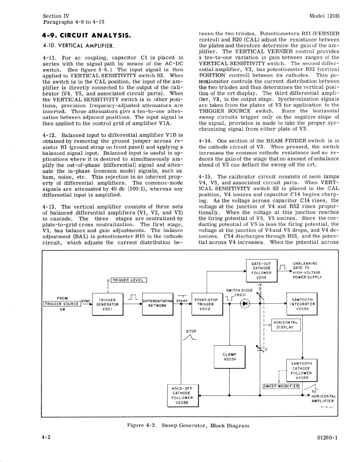
Overall Block Diagram 4Sweep Generator, Block Diagram 4-2
Sweep Generator Waveforms 4-3
Typical Schmitt Trigger 4-3
Low-Voltage Power Supply, Block
High-Voltage Power Supply, Block
120B Oscilloscope, Front View
Sweep or Single Sweep 3-3
......................
Input .3-4
......................
Input .3-5
Balance Adjustment 3-6
Diagram.
Diagram. .4-6
...............
...................
...................
...........
........
;
.
.
.
...........
.............
............
.....
........
...........
.4-5
LlST OF TABLES
1-1
22-2
3-2
Top View, Location of Parts and
1
1
Adjustments 5-3
High-Voltage Power Supply, Location
of Parts. 5-4
Vertical Sensitivity
Source
Parts and Adjustments
Right-Side View, Side Panel Removed,
Location of Parts and Adjustments 5-6
Servicing Etched Circuit Boards.
Vertical Amplifier, Schematic
Diagram 5 - 15
Horizontal Amplifier, Schematic
Diagram 5- 17
Sweep Generator, Schematic Diagram
Low-Voltage Power Supply, Schematic
Diagram 5 - 2
High-Voltage Power Supply, Schematic
Diagram 5- 23
Horizontal Display Switch, Schematic
Diagram. 5-25
..................
....................
(A21 and Trigger
(A201) Switches, Location of
...........
...
.....
.....................
.....................
.....................
.....................
....................
5-5
5-7
.
.
5-19
1
Number Title Page
1-1.
Specifications 1-0
Recommended Test Equipment
System Troubleshooting. 5-4
Adjustments Following Tube,
Transistor, and Diode Replacement.
Low-Voltage Power Supply Voltages
Horizontal Sweep-Time Adjustment.
Horizontal Sweep Time 5-14
Reference Designation Index
Replaceable Parts 6- 14
Code List of Manufacturers
..................
.......
...........
..
...
...
............
........
...............
.........
5-
1
5-8
5-9
5-12
6-
2
6-17
Page 5
Section I
1-
Table
Model 120B
1
Table
1- 1.
Specifications
SWEEP
Sweep Range:
One
p3ec/cm to
calibrated sweeps accurate to within
1,2,5,10.. . sequence, from 5 psec/cm to 200
millisec/cm. Vernier control permits continuous adjustment of sweep time between calibrated steps, and extends the 200
least 0.5 sec/cm.
Sweep Expand:
X5 sweep expansion may be used on all ranges
and expands fastest sweep to
panded sweep accuracy
Automatic Synchronization:
Internal: from signals 50 cps to 450 kc with
approximately 0.5-cm or more vertical deflection; and from line voltage.
External: from signal 50 cps to 450 kc, 1.5
peak-to-peak.
Trigger Point:
Zero-crossing negative slope of external sync
signals; or zero-crossing positive or negative
slope of vertical deflection signals. Front-panel
control overrides automatic and permits the
trigger point to be set between
Turning control fully counterclockwise restores
automatic operation.
at
least 0.5 sec/cm.
millisec/cm to at
1
is
*lo%.
psec/cm. Ex-
-7 to +7 volts.
Fifteen
*5%, in a
v
VERTICAL AMPLIFIER
Bandwidth: ating potential. Face plate eliminates glare and
DC coupled: dc to 450 kc. AC coupled: 2 cps reduces hazard of implosion. P2, P7, and
to 450 kc. Bandwidth
less of sensitivity setting.
Sensitivity:
10 millivolts/cm to 100 volts/cm. Four cali- divisions. Eliminates parallax error.
brated steps with attenuator accuracy of
10 mv/cm, 100 mv/cm, 1 v/cm, and 10 v/cm.
Vernier permits continuous adjustment of
tivity between steps, and extends 10
to at least 100
Internal Calibrator: 16-3/4
Calibrating signal automatically connected to deep, overall; hardware furnished for quick convertical amplifier for standardizing of gain, accuracy
Input Impedance
1
Balanced Input:
On 10 mv/cm range only; input impedance
megohms shunted by approximately 25 pf.
Common-Mode Rejection: 06. Rear terminals in parallel with front.
Rejection at least 40 db. Common mode signal 10. Provision for single sweep operation.
must not exceed
+2%.
megohm, shunted by approximately 50 pf.
v/cm.
:
is
at least 450 kc regard-
+3 volts peak.
*3%,
sensi-
v/cm step
is
2
Phase Shift:
Vertical and horizontal amplifiers have same
phase characteristics within
verniers are in CAL.
+ZO
to 100 kc when
HORIZONTAL AMPLIFIER
Bandwidth:
DC coupled: dc to 300 kc. AC coupled: 2 cps
to 300 kc. Bandwidth
less of attenuator setting.
Sensitivity:
0.1 volt/cm to 100 volts/cm. Three calibrated
steps, accurate within
and 10 v/cm. Vernier permits continuous adjustment of sensitivity between steps and
tends 10
Input Impedance
1
megohm nominal, shunted by approximately
100 pf.
Phase Shift:
Horizontal and vertical amplifiers have same
phase characteristics within
verniers are in CAL.
v/cm step to at least 100 v/cm.
:
is
at
least 300 kc regard-
&5%,
0.1 v/cm, 1 v/cm,
k2O to 100 kc when
GENERAL
Cathode Ray Tube:
P31 phosphor, mono-accelerator with internal
graticule normally supplied; 2700-volt acceler-
phosphors also available.
Internal Graticule:
10 cm x 10 cm marked in cm squares. Major
horizontal and vertical axes have 2-mm
Intensity Modulation:
Terminals on front panel. Plus 20 volt pulse
required to blank trace of normal intensity.
Dimensions:
in.
wide, 7-1/2 in. high, 18-3/8
version to 7 in. x 19 in. rack mount.
Weight:
Net: 32 lbs; shipping 45 lbs.
Power:
115 or 230 volts
mately 95 watts.
Options
:
05. External graticule crt with P31 phosphor.
13. Special front panel for rack mounting only.
*lo%,
50 to 1000 cps, approlci-
ex-
PI1
sub-
in.
Page 6
Model 120B
Paragraphs
Section
1-1
to 1-8
I
SECTION
GENERAL INFORMATION
1-1. INTRODUCTION.
1-2. This manual provides complete instructions on
the installation, operation, theory of operation, and
maintenance of the Hewlett-Packard Model 120B Os-
cilloscope.
1-3. The Hewlett-Packard Company uses a
section, eight-digit serial number (e. g. 000-00000).
If
the serial prefix (first three digits) on your instru-
ment does not agree with the prefix shown on the title
page of this manual, refer to either the separate
I,
change sheet included or Appendix
changes required to adapt this manual
prefixes. The separate change sheet also contains
corrections required for all known errata (errors).
Contact your Hewlett-Packard
if
additionalinformation or clarification is required.
Sales/Service Office
which contain
to
1-4. DESCRIPTION.
1-5. The Model 120B
scope whose bandwidth extends from dc to 450 kc. It
combines the precision characteristics of calibrated
is
a general-purpose oscillo-
two-
the listed
I
horizontal sweeps, calibrated vertical sensitivity,
a
crt that eliminates parallax error; in addition,
and
its construction provides easy circuit accessibility
and quick convertibility from a rack-mounting to a
bench-model configuration. Specifications are listed
in table
1-6. The internal graticule of the Model 120B
the same plane as the phosphor and crt trace; consequently, crt parallax error
quicker, and more accurate measurements.
1-7. The Model 120B can be used with either internal
or external sweeps, which can be either internally or
externally synchronized. Because of
tivity and balanced input, the Model 120B can be used
to view complex waveforms and monitor transducer
outputs.
1-8. Computations are avoided and possibilities of
error are reduced by direct-reading calibrated sweeps.
A
between the ranges
1-1.
is
in
is
avoided, allowing easier,
its
high sensi-
single control selects 1 of 15 calibrated sweeps
microseconds/cm and 200
of 5
Figure
1-
1.
Model 120B Oscilloscope
1-1
Page 7
Section I
Paragraphs 1
-
9 to 1 - 18
Model 120B
milliseconds/cm or determines the calibrated sensitivity of the horizontal amplifier. Continuous control
of sweep time and horizontal sensitivity between cali-
brated steps is provided
vernier control extends the 200
sweep time to at least 0.5 seconds/cm, and reduces
the horizontal amplifier sensitivity to at least 100
volts/cm.
1-9. Accurate direct-reading sweeps are obtained
from a feedback type (Miller) integrator, which en-
sures high linearity and stability of the horizontal
sweep. This type of sweep generator is reliable and
relatively independent of vacuum-tube characteristics.
1-
10. Observation and analysis of transients are simplifiedby the expanded-sweep control. This X5 sweep
expander may be used on all sweep time settings, and
expands the fastest sweep time to
1-
11.
An automatic trigger capability facilitates establishinga base line on the crt when a synchronizing
signal is not present. The automatic baseline provision can be easily locked-out and an adjustable trigger level established.
1-
12. Accurate voltage measurements of waveforms
are quickly made with the Model
calibrator that
mits rapid verification and standardization of vertical
amplifier sensitivity.
1-13. Phase-shift measurements can be made accurately over a wide range of input frequencies. Relative phase shift between the vertical and horizontal
amplifiers is less than 2 degrees up to 100 kc.
is
accurate to within *2 percent per-
by
a vernier control; the
milliseconds/cm
1
microsecond/cm.
120B. A built-in
1-14. CATHODE RAY TUBE WARRANTY.
1-15. The cathode ray tube supplied with the Model
120B and replacement crt's purchased from HewlettPackard Company are guaranteed against electrical
failurefor one year from the date of sale by HewlettPackard. The Cathode Ray Tube Warranty and Claim
sheet is included at the rear of this manual.
1-19. OPTION 06.
connectors in parallel with the front panel input connectors.
VERTICAL input terminals on the front panel, and
one connector is
TAL input terminals as shown in figures 5-6 and
Mating connectors and cable clamps are also supplied.
The additional circuitry changes the vertical input
capacitance to approximately
input capacitance to approximately 135 pf.
1-20. OPTION 10.
single sweep operation.
contained in figure 3-2 and a schematic for the added
circuit is shown in figure 5-8.
1-21. OPTION 13. This option provides a plain
7 x 9 x 3/16 inch front panel for rack mounting only.
The panel is suitablefor installing special handles to
match existing equipment in system or console
configuration.
1-22. AMBER FILTER.
supplied with oscilloscopes having an internal graticule
crt with
for improved visual observation of displays such as
single-shot phenomena or very low frequency applica-
tions.
characteristics desired for visualobservations of this
type display.
a. Remove front panel crt bezel.
b. Set filter into bezel, aligning larger rectangular
slots in the edge of filter with metal guide posts of the
bezel casting.
c. Remove oscilloscope top cover for access to
rear of crt.
d. Carefully move crt towardrear of instrument
enough to provide clearance for thickness of installed
filter (about 1/8 inch).
One connector is wired in parallel with the
P7 phosphor.
The filter will improve the long persistency
To install the filter proceed as follows:
This option provides rear panel
wiredin parallel with the HORIZON-
5-
75pf, and the horizontal
Thisoptionprovides circuitry for
Operation procedures are
A special amber filter is
This filter may be installed
7.
1-16. OPTIONS.
1-
17. The Model 120B is available with four options,
as
listed in table
are listedunder MISCELLANEOUS at the end of table
6-1.
1-18. OPTION 05. This optionprovides a crt without
internal graticule.
able illumination
Refer to figure 5- 9 for
CRT's without internal graticule are available with
types P7,
plied with each crt; amber for
type, and green for P31 type.
1-
1.
Replaceable parts for alloptions
An
external graticule with adjust-
is
installed over the face of the crt.
a
schematic of the added circuit.
P11, andP3l phosphor. Afilter
P7 type, blue for PI1
is
also sup-
e. Loosen clamp at socket of crt.
f.
Replace bezel with filter and tighten bezel
screws.
g. Slide crt forward until light mask on front of crt
just lightly touches filter.
h. Tighten clamp just enough to keep crt from turn-
ing.
Do not over-tighten the clamp or tube damage
may result.
i. Check alignment of trace with graticule accord-
ing to theprocedure given in Section V of this manual.
Page 8
Model 120B
Paragraphs 2-1 to 2-9
Section
I1
SECTION
INSTALLATION
2-1.
INCOMING INSPECTION.
2-2. MECHANICAL INSPECTION. Unpack and inspect the Model 120B in the presence of the carrier.
Be careful when unpacking the instrument, for all
electron tubes including the cathode ray tube remain
installed during shipment. Save all packing materials
until inspection
be required for reshipment in the event shipping dam-
is
age
age in shipment such as scratched panel, broken
knobs, etc.
check it operationally (see paragraph
claim with the carrier. Refer to the Hewlett-Packard
Warranty sheet at the front of this manual.
2-5. PERFORMANCE CHECK. Paragraph 5-52 contains performance check procedures for verifying
operation within listed specifications. The performance check is recommended for inclusion in receiving quality-control inspection. The following proce-
dure
operation.
2-6. INITIAL TURN ON. Energize the 120B as
follows:
power cable.
LISECONDS/CM position.
POSITION controls.
If
adjust position controls as necessary.
adjust HORIZONTAL POSITION to place left end of
sweep on left-end graticule line.
discovered.
2-3. Inspect the instrument for signs of possible dam-
If
2-4.
a. Turn INTENSITY control to OFF and plug in
b.
c. Set HORIZONTAL DISPLAY switch to 0.5
d. Center HORIZONTAL POSITION and VERTICAL
e. Turn 120B on and allow
f
g. Rotate INTENSITY clockwise until trace appears.
h. Adjust FOCUS for thin, -well-defined trace, and
there are any indications of damage, file a
is
offered, however, as a means to check basic
Set SWEEP MAGNIFIER switch to X1 position.
.
Set TRIGGER LEVEL to AUTO.
crt remains blank, press BEAM FINDER and re-
is
complete. These materials may
If
possible, energize the equipment and
2-
5).
two
minutes warmup.
MIL-
II
230
VOLTS AC
115
VOLTS AC
:41
Figure 2-
I
2
3
4
1L
230 VOLT CONNECTION
I
2
3
4
115
VOLT CONNECTION
1.
Primary-Power Connections
T302
T 302
LO-S-529
2-7.
2-8. The Model 120B requires a power source of 115
or 230 volts
can deliver approximately 95 watts. The oscilloscope
is
with a 115-volts power source. To convert the in-
strument for use with a 230-volt source, change the
dual primary windings of transformer T302 from a
parallel combination to a series combination. Figure
2-1 illustrates the connection for 115- and 230-volt
operation. At the time of the change, replace the
1.5-ampere slow-blow line fuse with 1-ampere
blow fuse.
POWER REQUIREMENTS.
?lo%,
single phase, 50 to 1000 cps, which
normally shipped from the factory wired for use
slow-
2-9.
For the protection of operating personnel, the
National Electrical Manufacturers' Assn (NEMA)
recommends that the instrument panel and cabinet
be grounded. This instrument is equipped with a
three-conductor power cable which, when plugged into
an appropriate receptacle, grounds the instrument.
The offset pin on the power cable three-prong connector is the ground pin. To preserve the protection
feature when operating the instrument from a
contact outlet, use a three-prong to two-prong adapter and connect the green pigtail on the adapter to
ground.
two-
Page 9
Section
II
Paragraphs 2-10 to 2-14
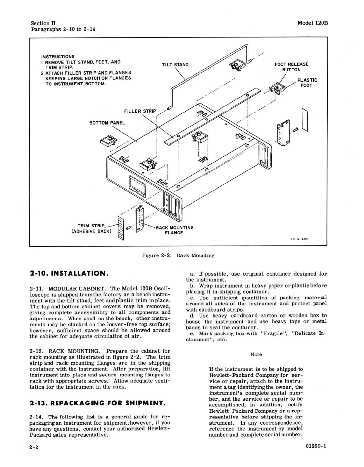
INSTRUCTIONS
I. REMOVE TILT STAND, FEET, AND
TRIM STRIP.
2.ATTACH FILLER STRIP AND FLANGES
KEEPING LARGENOTCHONFLANGES
TO INSTRUMENT BOTTOM.
Model 120B
FILLER STRIP
RACK MOUNTING
Figure 2-2. Rack Mounting
2-10. INSTALLATION.
2-11. MODULAR CABINET. The Model l2OB Oscil-
is
loscope
ment with the tilt stand, feet andplastic trim
shipped fromthe factory as a bench instru-
inplace.
The top and bottom cabinet covers may be removed,
giving complete accessibility to all components and
adjustments. When used on the bench, other instru-
be
ments may
stacked on the louver-free top surface;
however, sufficient space should be allowed around
the cabinet for adequate circulation of air.
2-12.
RACK
MOUNTING. Prepare the cabinet for
rack mounting as illustrated in figure 2-2. The trim
strip and rack-mounting flanges are in the shipping
container with the instrument. After preparation, lift
instrument into place and secure mounting flanges to
rack with appropriate screws. Allow adequate ventilation for the instrument in the rack.
2-13. REPACKAGING FOR SHIPMENT.
2-14. The following
packagingan instrument for shipment; however,
have any questions, contact your authorized
Packard sales representative.
list
is
a general guide for re-
Hewlett-
if
you
LO-M-489
a.
If
possible, use original container designed for
the instrument.
b. Wrap instrument
in
heavy paper or plastic before
placing it in shipping container.
c. Use sufficient quantities of packing material
around all sides of the instrument and protect panel
with cardboard strips.
d. Use heavy cardboard carton or wooden box to
house the instrument and use heavy tape or metal
bands to seal the container.
e. Mark packing box with "Fragile", "Delicate Instrument", etc.
Note
If
the instrument
is
to be shipped to
Hewlett-Packard Company for ser-
vice or repair, attach to the instru-
ment atag identifyingthe owner, the
instrument's complete serial number, and the service or repair to be
accomplished; in addition, notify
Hewlett-Packard Company or a representative before shipping the instrument. In any correspondence,
reference the instrument by model
number and complete serial number.
Page 10
Model 120B
Section
Paragraphs 3- 1 to 3-16
III
SECTION
OPERATION
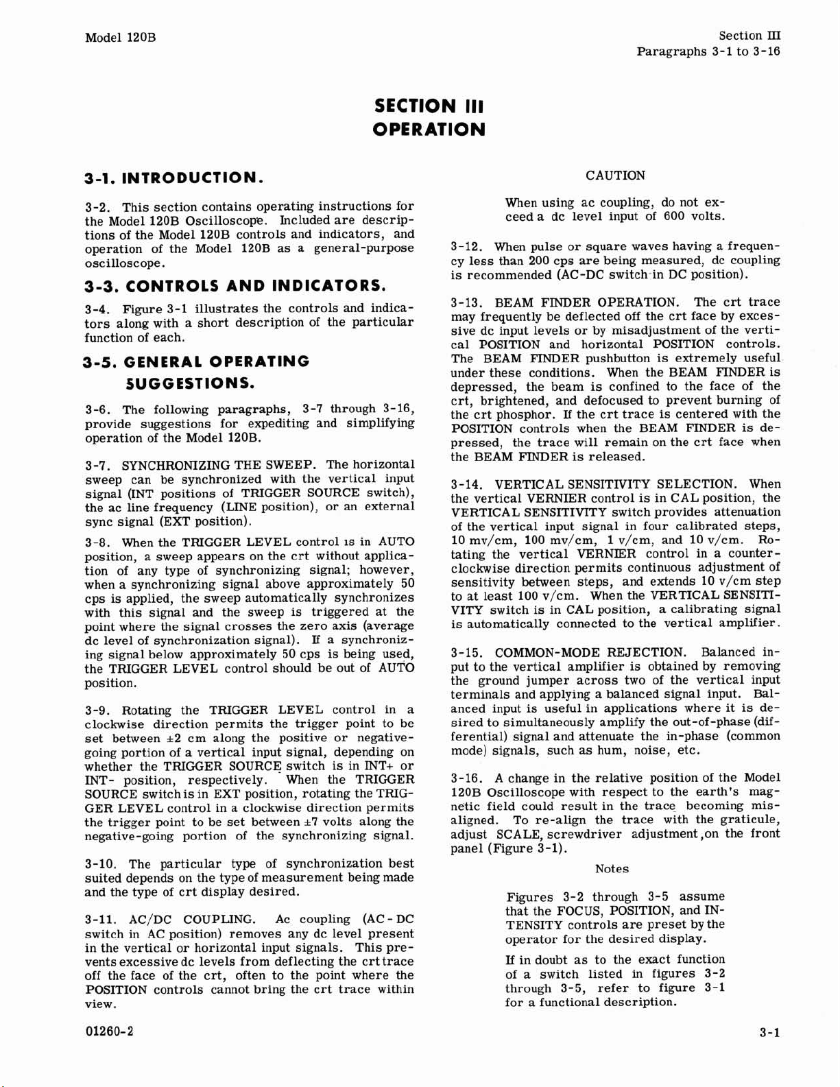
3-2. This section contains operating instructions for
the Model 120B Oscilloscope. Included are descriptions of the Model 120B controls and indicators, and
operation of the Model
oscilloscope.
3-3.
CONTROLS AND INDICATORS.
Figure 3-1 illustrates the controls and indica-
3-4.
tors along with a short description of the particular
function of each.
3-5, GENERAL OPERATING
SUGGESTIONS.
3-6. The following paragraphs, 3-7 through 3-16,
provide suggestions for expediting and simplifying
operation of the Model
3-7. SYNCHRONIZING THE SWEEP. The horizontal
sweep can be synchronized with the vertical input
signal (INT positions of TRIGGER SOURCE switch),
the ac line frequency (LINE position), or an external
sync signal (EXT position).
3-8. When the TRIGGER LEVEL control
position, a sweep appears on the crt without application of any type of synchronizing signal; however,
when a synchronizing signal above approximately 50
cps is applied, the sweep automatically synchronizes
with this signal and the sweep
point where the signal crosses the zero axis (average
dc level of synchronization signal).
ing signal below approximately 50 cps
the TRIGGER LEVEL control should be out of AUTO
position.
3-9. Rotating the TRIGGER LEVEL control in a
clockwise direction permits the trigger point to be
set between
going portion of a vertical input signal, depending on
whether the TRIGGER SOURCE switch is in
INT- position, respectively. When the TRIGGER
SOURCE switch
GER LEVEL control in a clockwise direction permits
the trigger point to be set between
negative-going portion of the synchronizing signal.
3-10. The particular type of synchronization best
suited depends on the type of measurement being made
and the type of crt display desired.
3-11.
switch in AC position) removes any dc level present
in the vertical or horizontal input signals. This prevents excessive dc levels from deflecting the crt trace
off the face of the crt, often to the point where the
POSITION controls cannot bring the crt trace within
view.
rt2 cm along the positive or negative-
is
in EXT position, rotating the TRIG-
AC/DC COUPLING. Ac coupling (AC - DC
120B as a general-purpose
120B.
is
in AUTO
is
triggered at the
If
a synchroniz-
is
being used,
INT+ or
rt7 volts along the
Ill
CAUTION
When using ac coupling, do not
ceed a dc level input of 600 volts.
3-12. When pulse or square waves having a
cy less than 200 cps are being measured, dc coupling
is recommended (AC-DC switch-in DC position).
3-13. BEAM FINDER OPERATION. The crt trace
may frequently be deflected off the crt face by excessive dc input levels or by misadjustment of the vertical POSITION and horizontal POSITION controls.
The BEAM FINDER pushbutton is extremely useful
under these conditions. When the BEAM FINDER
depressed, the beam is confined to the face of the
crt, brightened, and defocused to prevent burning of
the crt phosphor.
POSITION controls when the BEAM FINDER
pressed, the trace will remain on the crt face when
the BEAM FINDER
3-14. VERTICAL SENSITIVITY SELECTION. When
the vertical VERNIER control
VERTICAL SENSITIVITY switch provides attenuation
of the vertical input signal in four calibrated steps,
10
mv/cm, 100 mv/cm, 1 v/cm, and 10 v/cm.
tating the vertical VERNIER control in a counter-
clockwise direction permits continuous adjustment of
sensitivity between steps, and extends 10
at
least 100 v/cm. When the VERTICAL SENSITI-
to
VITY switch
is automatically connected to the vertical amplifier.
3
-
15. COMMON-MODE REJECTION. Balanced input to the vertical amplifier
the ground jumper across two of the vertical input
terminals and applying a balanced signal input. Balanced input
sired to simultaneously amplify the out-of-phase (differential) signal and attenuate the in-phase (common
mode) signals, such as hum, noise, etc.
3-16. A change in the relative position of the Model
120B Oscilloscope with respect to the earth's magnetic field could result in the trace becoming misaligned. To re-align the trace with the graticule,
adjust SCALE, screwdriver adjustment ,on the front
panel (Figure 3-1).
Figures 3-2 through 3-5 assume
that the FOCUS, POSITION, and INTENSITY controls are preset by the
operator for the desired display.
If
in doubt as to the exact function
of a switch listed in figures 3-2
through 3-5, refer to figure 3-1
for a functional description.
If
the crt trace
is
released.
is
in CAL position, a calibrating signal
is
useful in applications where it
Notes
is
is
in CAL position, the
is
obtained by removing
ex-
frequen-
is
centered with the
is
de-
Ro-
v/cm step
is
de-
Page 11
Section
III
Figure 3-
Model 120B
1
7
-4
0.c
HEWLC
20 19
1.
FOCUS: Controls crt focus.
18
I7 16 15
11.
14
13 12
11
10 9 8
MP-M-
Vertical POSITION: Controls verticalposition of crt display.
2. Horizontal VERNIER: Adjusts sensitivity
between ranges; in CAL position, deflec-
tion
as
indicated
by
selected
VOLTS/CM
position of HORIZONTAL DISPLAY switch.
3. HORIZONTAL DISPLAY: 15 positions se- 13. SWEEP MAGNIFIER:
3
lect sweep speed,
positions select hori-
zontal deflection sensitivity.
4. TRIGGER LEVEL: Determines level of
trigger point on sync signal.
12. BAL: Adjust for no vertical shift with rotation of vertical VERNIER.
In
Xl position sweep
time selected by HORIZONTAL DISPLAY.
In
X5position sweep speed
is
5
times faster.
14. EXT. SYNC OR HORIZ: External sync or
horizontal amplifier input.
5. TRIGGER SOURCE: Four positions select
sweep synchronization. 15. Horizontal AC-DC: AC position input
itively coupled into horizontal amplifier.
6.
Vertical VERNIER: Adjusts sensitivity be-
DC position input directly coupled into hor-
tween ranges; in CAL position, deflection izontal amplifier.
as selected by VERTICAL SENSITMTY
switch. 16. Z AXIS: Input for crt intensity modulation
signal.
7. VERTICAL SENSITIVITY: Four positions
select deflection sensitivity. CAL position 17. Horizontal POSITION: Controls horizontal
displays internal calibrator signal.
position of crt display.
85
capac-
8.
CAL: Adjusts calibration of vertical input.
18.
BEAM FINDER: Returns beam to crt face
regardless of horizontal and vertical POSI-
9.
Vertical input terminals. TION settings.
10. Vertical AC-DC: AC position input capaci- 19. INTENSITY
tively coupled into vertical amplifier. DC
power and controls crt intensity.
&
POWER: Applies ac line
position input directly coupled into vertical
amplifier. 20. SCALE: Aligns trace with graticule.
Figure 3-1.
Model 120B Oscilloscope, Front View
01260-1
Page 12
Model
120B
Section
Figure
Ill
3-2
INTERNAL HORIZONTAL SWEEP:
1.
Set vertical AC-DC to desired type of input A. Set SWEEP switch to normal (N), TRIGGER
coupling.
2.
Set VERTICAL SENSITIVITY to desired vertical
sensitivity.
3.
Set vertical VERNIER to CAL for calibrated Minimum trigger sensitivity
SINGLE SWEEP (OPTION
SOURCE switch to EXT, and remove any external
trigger source.
B.
Adjust TRIGGER LEVEL control fully clockwise.
is
10):
obtained with the
sensitivity. control in this position.
4.
Set HORIZONTAL DISPLAY to desired horizontal
C. To increase trigger sensitivity, rotate TRIGGER
sweep time. Set VERNIER to CAL for calibrated LEVEL control counterclockwise. Maximum
sweep time.
X1
5. Set SWEEP MAGNIFIER to
6.
Set TRIGGERSOURCE to desired type of horizontal sweep synchronization.
or X5, as desired.
If
external sync
selected, connect sync signal to EXT. SYNC.
7.
Apply vertical input signal to vertical input
terminals.
8.
Adjust TRIGGER LEVEL for desired synchroni-
zation.
I
Figure
3-2.
Operation Using Internal'Horizontal Sweep or Single Sweep
is
sensitivity will be obtained just prior to the point
where the oscilloscope sweeps intermittently.
D. Set SWEEP switch to single (S). The instrument
is
now in the "armed" state and will sweep once
when triggered.
E. To rearm the sweep circuit, set SWEEP switch
from S to N and then back to S. External triggering
should not be applied during this operation to
vent the single sweep from occurring immediately
is
when the switch
returned to the S position.
pre-
Page 13
Section
III
Figure 3-3
SWEEP
MAGNIFIER
Model
120B
1.
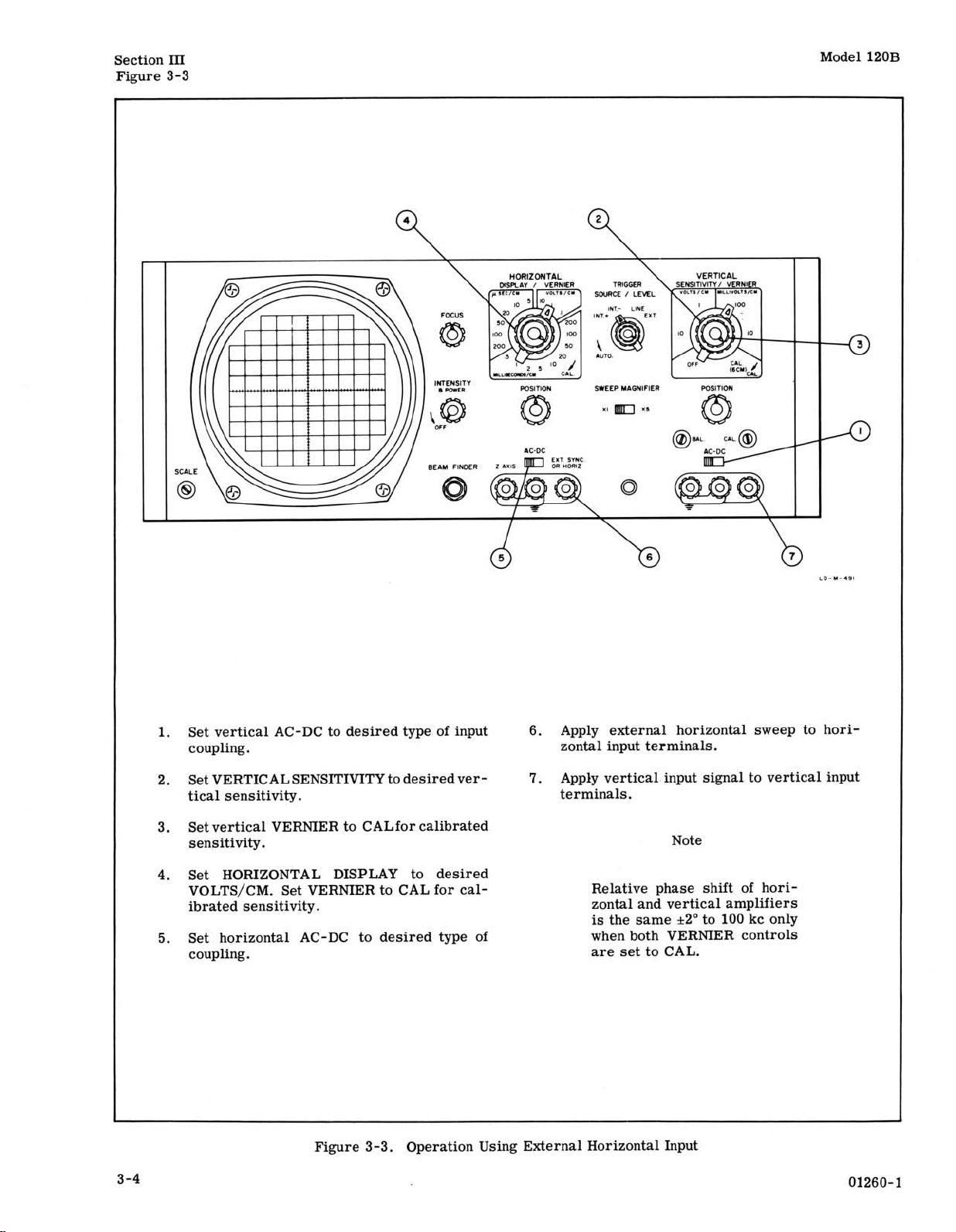
Set vertical AC-DC to desired type of input
6.
Apply external horizontal sweep to hori-
coupling. zontal input terminals.
2.
Set VERTICAL SENSITIVITY to desired ver-
7.
Apply vertical input signal to vertical input
tical sensitivity. terminals.
Set vertical VERNIER to
3.
CALfor calibrated
sensitivity. Note
4.
Set HORIZONTAL DISPLAY to desired
VOLTS/CM. Set VERNIER to CAL for calibrated sensitivity.
5.
Set horizontal AC-DC to desired type of
Relative phase shift of horizontal and vertical amplifiers
is
the same
+2"
to
100
kc only
when both VERNIER controls
coupling. are set to CAL.
Figure 3-3. Operation Using External Horizontal Input
3
-4
Page 14
Model 120B
SWEEP
MAGNIFIER
Section
111
Figure 3-4
Remove grounding strap from vertical in-
Set vertical AC-DC to desired type of input
1.
7.
coupling. put terminals.
2. Set VERTICAL
VOLTS/CM. (Input not balanced in any terminals;
other position of VERTICAL SENSITMTY nect
switch.
Set vertical VERNIER to CAL for calibrated
3.
)
sensitivity.
Set HORIZONTAL DISPLAY to desired hor- The common-mode input sig-
4.
izontal sweep speed.
SENSITIVITY to 10 MILLI-
8.
Connect vertical signal to vertical input
if
ac coupling
0. 1-uf 600-volt capacitor in series
with center vertical input terminal.
Note
nal voltage, either positive or
negative, must not exceed 3
5. Set SWEEP MAGNIFIER to
desired.
6. Set TRIGGER SOURCE to desired type of
X1 or X5, as volts minus the peak amplitude
of the differential input signal.
9.
Adjust TRIGGER LEVEL for desired syn-
horizontal sweep synchronization. chronization.
is
desired, con-
LO-U-.92
Figure 3-4. Operation Using Balanced Vertical Input
3-5
Page 15
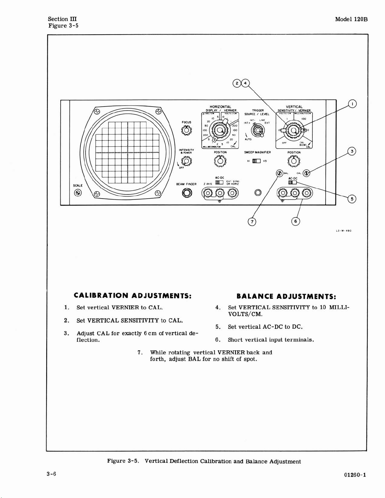
Section
Figure 3-5
III
Model 120B
SWEEP MAGNIFIER
CALIBRATION ADJUSTMENTS:
1.
Set vertical VERNIER to CAL.
2. Set VERTICAL SENSITIVITY to CAL.
Adjust CAL for exactly
3.
flection.
6
cm of vertical de-
While rotating vertical VERNIER back and
7.
forth, adjust BAL for no shift of spot.
BALANCE ADJUSTMENTS:
4.
Set VERTICAL SENSITIVITY to 10
VOLTS/CM.
Set vertical AC-DC to DC.
5.
6.
Short vertical input terminals.
LD-Y-490
MILLI-
Figure 3
-
5.
Vertical Deflection Calibration and Balance Adjustment
01260-1
Page 16
Model 120B
Section
IV
Paragraphs 4-1 to 4-8
SECTION
PRINCIPLES OF OPERATION
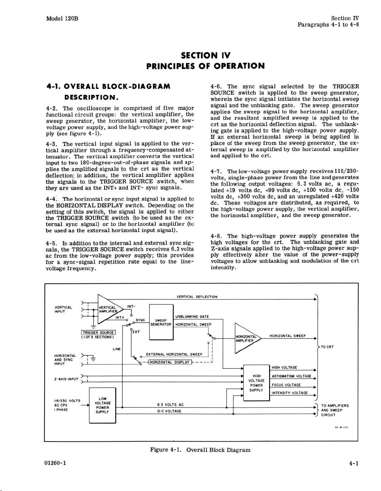
4-1.
OVERALL BLOCK-DIAGRAM
DESCRIPTION.
is
4-2. The oscilloscope
functional circuit groups:
sweep generator, the horizontal amplifier, the lowvoltage power supply, and the high-voltage power
ply (see figure 4-1).
4-3. The vertical input signal is applied to the vertical amplifier through a frequency -compensated
tenuator. The vertical amplifier converts the vertical
input to two 180-degree-out-of -phase signals and applies the amplified signals to the crt as the vertical
deflection; in addition, the vertical amplifier applies
the signals to the TRIGGER SOURCE switch, when
they are used
as
the INT+ and INT- sync signals.
4-41 The horizontal or sync input signal
the HORIZONTAL DISPLAY switch. Depending on the
setting of this switch, the signal is applied to either
the TRIGGER SOURCE switch (to be used as the external sync signal) or to the horizontal amplifier (to
be used as the external horizontal input signal).
In
4-5.
addition tothe internal and external sync sig-
nals, the TRIGGER SOURCE switch receives 6.3 volts
ac from the low-voltage power supply; this provides
a
sync-signal repetition rate equal to the line-
for
voltage frequency.
comprised of five major
the vertical
amplifier,
sup-
is
applied to
the
at-
IV
4-6. The sync signal selected by the TRIGGER
SOURCE switch is-applied to the sweep generator,
wherein the sync signal initiates the horizontal sweep
signal and the unblanking gate. The sweep generator
applies the sweep signal to the horizontal amplifier,
and the resultant amplified sweep
crt as the horizontal deflection signal. The unblank-
is
ing gate
If
an external horizontal sweep is being applied
applied to the high-voltage power supply.
place of the sweep from the sweep generator, the ex-
ternal sweep
is
amplified by the horizontal amplifier
and applied to the crt.
4-7. The low-voltage power supply receives
volts, single-phase power from the line andgenerates
the following output voltages: 6.3 volts ac, a regu-
lated +19 volts dc, +99 volts dc,
volts dc,
+300 volts dc, and an unregulated +420 volts
dc. These voltages are distributed, as required, to
the high-voltage power supply, the vertical amplifier,
the horizontal amplifier, and the sweep generator.
4-8. The high-voltage power supply generates the
high voltages for the
crt. The unblanking gate and
Z-axis signals applied to the high-voltage power .supply effectively alter the value of the power-supply
voltages to allow unblanking and modulation of the crt
intensity.
is
applied to the
in
115/230-
+I00 volts dc, -150
VERTICAL DEFLECTION
VERTICAL
GENERATOR HORIZONTAL SWEEP
(
I OF 3 SECTIONS
115/230 VOLTS
60 CPS 6 3 VOLTS AC
l PHASE
)
LOW
POWER
SUPPLY D-C VOLTAGE AND SWEEP
Figure 4-1. Overall Block Diagram
-
-+
HIGH VOLTAGE
POWER FOCUS VOLTAGE
SUPPLY
INTENSITY VOLTAGE
\
*
>TO CRT
b
+
1
CIRCUIT
80-"-266
4-1
Page 17
Section IV
Paragraphs 4-9 to 4-15
Model
120B
4-9.
CIRCUIT ANALYSIS.
4-10.
VERTICAL AMPLIFIER.
4-11. For ac coupling, capacitor C1
is
placed in
series with the signal path by means of the AC-DC
switch. (See figure 5-6.
applied to VERTICAL SENSITIVITY switch
the switch
is
in the CAL position, the input of the am-
)
The input signal
is
then
S2. When
plifier is directly connected to the output of the calibrator (V4, V5, and associated circuit parts). When
is
the VERTICAL SENSITIVITY switch
in other positions, precision frequency-adjusted attenuators are
inserted. These attenuators give a ten-to-one attenuation between adjacent positions. The input signal
is
then applied to the control grid of amplifier VIA.
4-12. Balanced input to differential amplifier V1B
is
obtained by removing the ground jumper across resistor
R1 (ground strap on front panel) and applying a
balanced signal input. Balanced input is useful in applications where it
is
desired to simultaneously amplify the out-of-phase (differential) signal and attenuate the in-phase (common mode) signals, such as
hum, noise, etc. This rejection
is
an inherent property of differential amplifiers. The common-mode
signals are attenuated by 40 db
differential input
is
amplified.
(100:1), whereas any
4-13. The vertical amplifier consists of three sets
of balanced differential amplifiers
(Vl, V2, and V3)
in cascade. The three stages are neutralized by
plate-to-grid cross neutralization. The first stage,
V1, has balance and gain adjustments. The balance
adjustment (BAL)
is
potentiometer R16 in the cathode
circuit, which adjusts the current distribution be-
tween the two triodes. Potentiometers
control) and
R20 (CAL) adjust the resistance between
R21 (VERNIER
the plates and therefore determine the gain of the amplifier. The VERTICAL VERNIER control provides
a
ten-to-one variation in gain between ranges of the
VERTICAL SENSITIVITY switch. The second differential amplifier,
V2, has potentiometer R32 (vertical
POSITION control) between its cathodes. This potentiometer controls the current distribution between
the two triodes and thus determines the vertical position of the crt display. The third differential
fler, V3,
is
the output stage. Synchronization signals
ampli-
are taken from the plates of V3 for application to the
TRIGGER SOURCE switch. Since the horizontal
sweep circuits trigger only on the negative slope of
the signal, provision is made to take the proper synchronizing signal from either plate of V3.
4-14. One section of the BEAM FINDER switch is in
the cathode circuit of V3.
When pressed, the switch
increases the common cathode resistance and so re-
duces the gain of the stage that no amount of unbalance
ahead of V3 can deflect the sweep off the crt.
4-15. The calibrator circuit consists of neon lamps
V4,
V5, and associated circuit parts. When VERT-
ICAL SENSITIVITY switch
S2 is placed in the CAL
position, V4 ionizes and capacitor C14 begins charg-
ing. As the voltage across capacitor C14 rises, the
voltage at the junction of V4 and R52 rises proportionally. When the voltage at this junction reaches
the firing potential of
ducting potential of V5
V5, V5 ionizes. Since the con-
is
less the firing potential, the
voltage at the junction of V4 and V5 drops, and V4 deionizes. C14 discharges through
R53, and the poten-
tial across V4 increases. When the potential across
FROM
ITRIGGER
SOURCE
SW
SYNC
I
-+
9
[TRIGGER LEVEL
I
I
I
TRIGGER
GENERATOR
v201
-
Figure
I
-
NETWORK
4-2.
TRIGGER
v202
STOP
A
HOLD-
OFF
CATHODE
FOLLOWER
V203B
Sweep Generator,
i
Block
SWITCH DIODE
CLAMP
V203A
A
-
Diagram
GATE-OUT
CATHODE
FOLLOWER
V204
-v
n
'
I V205A
I
I
I
I
:--
ISWEEP
MAGNIFIER]
*
-
UNBLANKING
GATE TO
HIGH-VOLTAGE
POWER SUPPLY
SAWTOOTH
*
INTEGRATOR
+
SAWTOOTH
CATHODE
FOLLOWER
V205B
-
A
TO
HORIZONTAL
AMPLIFIER
83-U-267
01260-1
Page 18
Model 120B
Section
IV
Paragraphs 4-16 to 4-22
GRlD OF
V201A
PLATE OF
V201B
JUNCTION
OF C207
C208
AND
PLATE OF
V202B
GRID OF
V203B
(SEE NOTE)
GRlD
OF
V202A
-1
'
-
I
I
I
I
I
I
I
I
I
I
I
I
I
I
I
I
I
I
1
I
I
I
I
I
I
I
I
I
LENGTH
OF
SAWTOOTH
TIME CONSTANT
ON RC
SELECTEDBY
HORIZONTAL
SWITCH
DISPLAY^
DEPENDS
LD-S-
530
the negative-going output
is
applied to switch diode
CR201.
4-19. Switch diode CR201 normally clamps the input
to sawtooth integrator
age, preventing sawtooth integrator
erating a sawtooth waveform. When the
going step signal from the start-stop trigger
to the switch diode, however, the diode
V205A to a low negative volt-
V205A from gen-
negative-
is
applied
is
reverse
biased and allows the sawtooth integrator to generate
a sawtooth waveform.
4-20. The sawtooth output of
V205B
applied to the horizontal amplifier to serve
is
simultaneously
as
the
horizontal sweep signal and the hold-off cathode fol-
V203B. The output of the hold-off cathode fol-
lower
lower
is
applied to the input of the start-stop trigger
terininate the sweep. The values of R and C selected
to
by the HORIZONTAL DISPLAY switch determines the
slope of the
Clamp V204 ensures that the sawtooth always
sweepand therefore the time of the sweep.
starts
at the same level. Figure 4-3 shows the relative
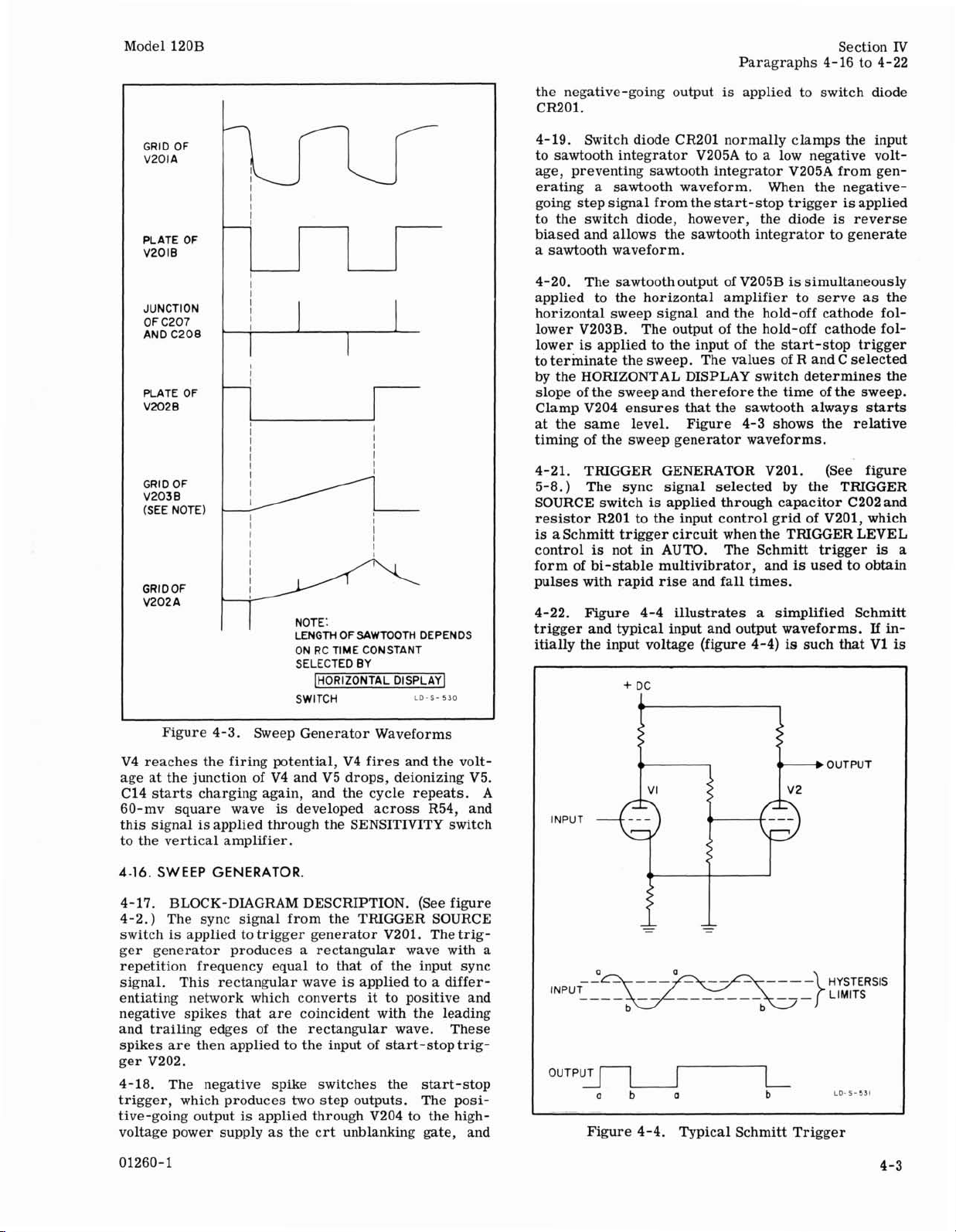
timing of the sweep generator waveforms.
4-21. TRIGGER GENERATOR V201. (See figure
5-8.)
SOURCE switch
resistor
is
control
form of bi-stable multivibrator, and
The sync signal selected by the TRIGGER
is
applied through capacitor C202 and
R201 to the input control grid of V201, which
a Schmitt trigger circuit when the TRIGGER LEVEL
is
not in AUTO. The Schmitt trigger
is
used to obtain
is
pulses with rapid rise and fall times.
4-22. Figure 4-4 illustrates a simplified Schmitt
If
trigger and typical input and output waveforms.
is
itially the input voltage (figure 4-4)
+
DC
such that V1
in-
is
a
Figure 4-3. Sweep Generator Waveforms
V4 reaches the firing potential, V4 fires and the volt-
4
b
(w
OUTWT
age at the junction of V4 and V5 drops, deionizing V5.
C14 starts charging again, and the cycle repeats. A
is
60-mv square wave
this signal
is
applied through the SENSITIVITY switch
developed across R54, and
I
INPUT
v2
v
to the vertical amplifier.
4-16.
SWEEP GENERATOR.
4-17. BLOCK-DIAGRAM DESCRIPTION. (See figure
4-2.) The sync signal from the TRIGGER SOURCE
is
switch
applied to trigger generator V201. The trig-
-
-
-
-
-
ger generator produces a rectangular wave with a
repetition frequency equal to that of the input sync
signal. This rectangular wave is applied to a differ-
it
entiating network which converts
to positive and
negative spikes that are coincident with the leading
and trailing edges of the rectangular wave. These
spikes are then applied to the input of start-stop trigger V202.
4-18. The negative spike switches the start-stop
trigger, which produces two step outputs. The posi-
is
tive-going output
applied through V204 to the high-
-
ob
-
-
a
I
b
LO 5-53!
voltage power supply as the crt unblanking gate, and Figure 4-4. Typical Schmitt Trigger
Page 19
Section IV
Paragraphs 4-23 to 4-32
Model 120B
cutoff, V2 conducts. As the input voltage becomes
more positive, it eventually reaches a predetermined
level (a) at which the circuit changes state; that
V1 conducts and V2
goes negative, the common cathode potential decreases
and the grid of V2 becomes positive. When the input
reaches a second predetermined level
and the circuit switches back to
output of the circuit
or negative depending upon the slope of the input
signal.
4-23. The input voltage levels at which a Schmitt
trigger circuit switches are called the hysteresis
limits. Note that the circuit (figure 4-4) does not
switch unless the input crosses both limits.
4-24. Trigger generator V201 has some additional
features: the TRIGGER LEVEL control adjusts the
bias on
input trigger must reach to change state; in addition,
when the TRIGGER LEVEL control
limit, switch S202
shunt across resistor R207 and capacitors C205 and
C206, and the trigger generator becomes an astable
multivibrator. This provides triggers to the
start trigger even though no sync is applied to the
trigger generator. When a sync signal above approxi-
mately 50 cps
erator then synchronizes with the sync signal. The
step output of the trigger generator
plate of
4-25. DIFFERENTIATING NETWORK. (See figure
5-8.) The differentiating network
series combination of capacitor
and resistor R210. The r-c time constant of this network
the trigger generator output pulses; consequently, the
signal developed across inductor L201 and resistor
R210 consists of short negative and positive spikes
that are coincident with the leading and trailing edges
of the trigger generator output pulses. These spikes
are coupled through capacitor C208 to the control grid
of
4-26. START-STOPTRIGGER
AND SWITCH DIODE CR201. -(See figure 5-8. ) The
start-stop trigger is a Schmitt trigger circuit. A
typical Schmitt trigger
V202 is triggered by a negative spike pulse from the
differentiating network. One output step waveform is
taken from the plate of
plies to switch diode
V203A. The waveform applied to V203A cuts off
V203A, and thus disables the clamping action of this
tube. The waveform applied to switch diode
reverse-biases the diode, and thus it ceases conduction. Another step output
V202A and applied through cathode follower V204 to
the high-voltage power supply; this serves as the crt
unblanking gate.
4-27. SAWTOOTH GENERATOR
TOOTH CATHODE FOLLOWER
V2OlA and thus determines the level which the
V201B andapplied to a differentiating network.
is
extremely small compared with the width of
V202A, one half of the start-stop trigger.
is
cutoff.
is
a voltage step, either positive
is
placed in AUTO. This opens the
is
applied, however, the trigger gen-
is
V202B and simultaneously ap-
CR201 and the grid of clamp
If
the input voltage then
(b),
V2 conducts
its
initial state. The
is
at its extreme
is
taken from the
is
composed of the
C207, inductor L201,
V202, CLAMP V203A,
described in paragraph 4-22.
is
taken from the plate of
V205A AND SAW-
V205B. (See figure
is,
stop-
CR201
5-8.) Sawtooth generator
tegrator which produces a linear sawtooth waveform.
When switch diode
tegrating capacitor charges through the integrating
resistance, producing a negative-going potential at
the control-grid of
the plate of
cathode follower
completing the negative feedback required by this
Miller type integrator.
4-28. The sawtooth signal at the cathode of
also applied to SWEEP MAGNIFIER switch S102.
When ,9102
to the horizontal amplifier has
times greater than that applied when S102
position; hence, the angle of slope is increased five
times and the sweep time
by the HORIZONTAL DISPLAY switch.
4-29. The sawtooth signal at the cathode of
applied to the control grid of V202A. When the slope
of the signalreaches the upper hysteresis limit of the
start-stop trigger, the trigger changes state; hence,
the unblanking gate output of
The switch diode
respectively, halting the charging of the integrating
capacitor and terminating the sawtooth waveform.
The hold-off capacitor in the cathode of
during the rising slope of the signal output of the
off cathode follower but does not immediately discharge when the sawtooth input to the hold-off cathode
follower terminates. This prevents the start-stop
trigger from again being triggered by a negative spike
until the sweep circuits have fully recovered. A different value of hold-off capacity
setting of the HORIZONTAL DISPLAY switch.
4-30.
4-31. The grid of VlOlA (figure 5-7) receives either
the sweep output from the horizontal sweep circuits
or from an external sweep source, depending on the
setting of the HORIZONTAL DISPLAY switch. When
external sweep is being used (EXT SENSITIVITY positions), any one of three horizontal sweep sensitivities
can be selected:
VOLTS/CM. The AC-DC switch allows selection of
direct coupling, or ac coupling through capacitor
C101.
4-32. The horizontal amplifier consists of two differential amplifiers
the HORIZONTAL DISPLAY switch
EXT SENSITIVITY positions, the resistance between
the cathodes of amplifier VlOl consists of the horizontal VERNIER control
horizontal gain control
R107 is between the cathodes. The horizontal POSITION control (potentiometer
of VlOl controls the horizontal position of the crt
trace. The second stage
plate-to-grid cross neutralization. The output of the
horizontal amplifier
and applied directly to the horizontal deflection plates
of the crt.
V205A
is
HORIZONTAL AMPLIFIER.
CR201 ceases conduction, the in-
V205A. The amplified signal at
is
V205B to the integrating capacitor,
in the X5 position, the sawtooth applied
CR20l and clamp V204 again conduct,
.1
VOLTS/CM, 1 VOLTS/CM, or 10
(V101 and V102) in cascade. When
is
V205A is a Miller in-
coupled back through sawtooth
V205B
a
peak amplitude five
is
in the X1
is
one-fifth of that selected
V203B
V203A is terminated.
V203B charges
is
selected for each
is
set to one of the
(R275B) in series with the
(R104); otherwise, resistor
R109) between the plates
(V102)
taken from the plates of V102
is
neutralized by
is
is
hold-
Page 20
Model 120B
Section
Paragraphs 4-33 to 4-40
IV
+I9 VOLT DC
AC
b
REGULATED
POWER SUPPLY
-
115/230 VOLTS
60
CPS
IPHASE
4-33.
the cathode circuit of
increases the common cathode resistance and so reduces the gain of the stage that no amount of unbalance
ahead of V102 can deflect the sweep off the crt.
4-34.
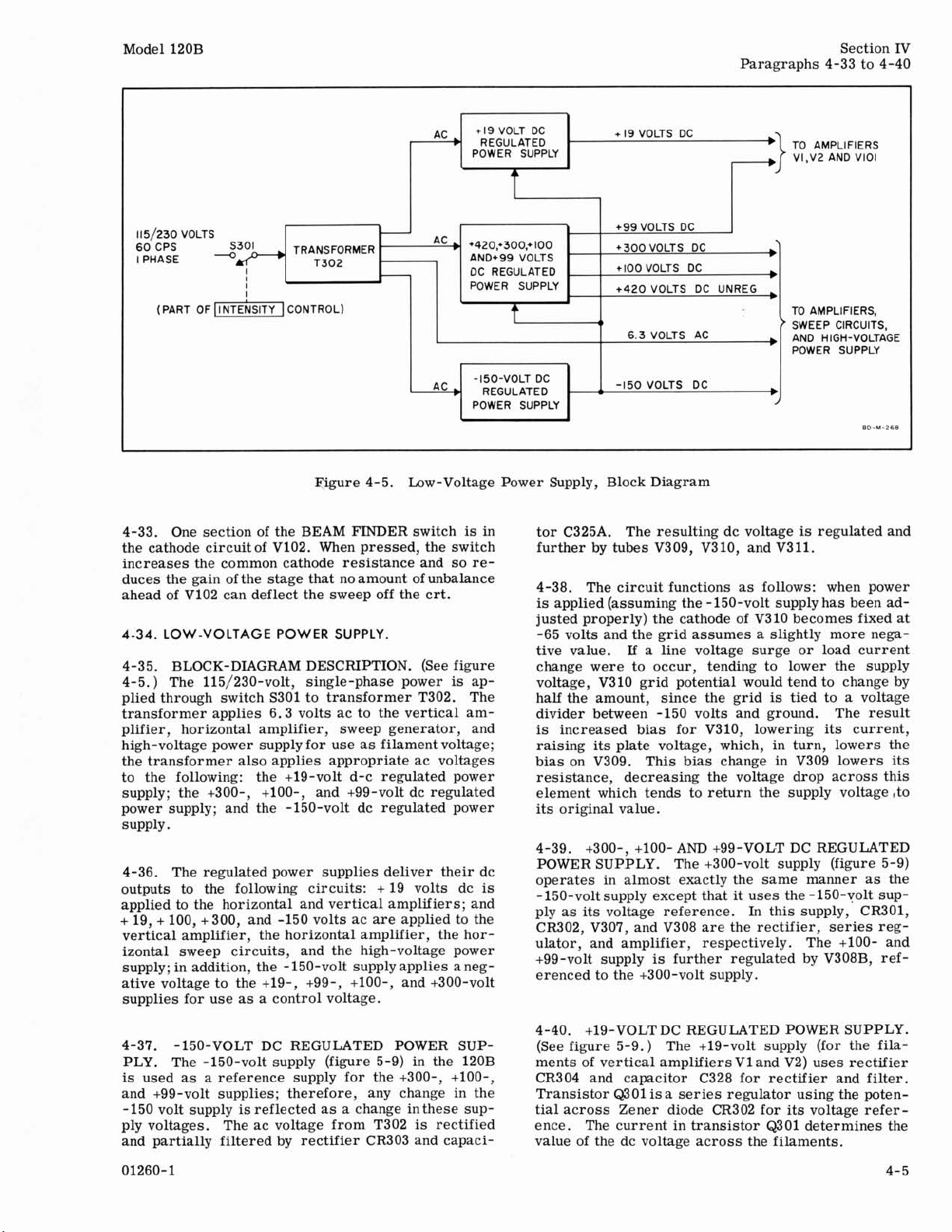
4-3 5. BLOCK-DIAGRAM DESCRIPTION. (See figure
4-5.) The
plied through switch S301 to transformer
transformer applies 6.3 volts ac to the vertical amplifier, horizontal amplifier, sweep generator, and
high-voltage power supply for use as filament voltage;
the transformer also applies appropriate ac voltages
to the following: the
supply; the
power supply; and the -150-volt dc regulated power
supply.
4-36. The regulated power supplies deliver their dc
outputs to the following circuits:
applied
'I9, + loo,
vertical amplifier, the horizontal amplifier, the hor-
izontal sweep circuits, and the high-voltage power
supply; in addition, the -150-volt supply applies
ative
supplies for use as a control voltage.
One section of the BEAM FINDER switch
LOW-VOLTAGE POWER SUPPLY.
to
voltage to the +19-. +99-. +loo-. and +300-volt
S301
--
I
I
I
115/230-volt, single-phase power is ap-
+300-, +loo-, and +99-volt dc regulated
the horizontal and vertical amplifiers; and
+300,
TRANSFORMER
T302
Yigure 4-5. Low-Voltage Power Supply, Block Diagram
V102. When pressed, the switch
+19-volt d-c regulated power
and
-
-
-
b
T302. The
+
19 volts dc is
are
'
to
aneg-
+420,*300,+
AND199 VOLTS
OC REGULATED
POWER SUPPLY
-150-VOLT DC
POWER SUPPLY
is
the
T
100
t
REGULATED
in
tor C325A. The resulting dc voltage
further by tubes
4-38. The circuit functions as follows: when power
is
justed properly) the cathode of V310 becomes fixed at
-65 volts and the grid assumes a slightly more negative value.
change were to occur, tending to lower the supply
voltage, V310 grid potential would tend to change by
half the amount, since the grid
divider between -150 volts and ground. The result
is
raising
bias on
resistance, decreasing the voltage drop across this
element which tends to return the supply voltage
its original value.
4-39.
POWER
operates in almost exactly the same manner as the
-
150-volt supply except that it uses the - 150-volt sup-
ply
CR302, V307, and V308
ulator, and amplifier, respectively. The
+99-volt supply is further regulated by V308B, referenced to the +300-volt supply.
+
19
VOLTS DC
TO AMPLIFIERS
VI,V2 AND VlOl
2)
+99VOLTS DC
+300 VOLTS DC
+I00 VOLTS DC
+420VOLTS DC UNREG
TO AMPLIFIERS,
6.3 VOLTS AC AND HIGH-VOLTAGE
-150 VOLTS DC
V309, V310, and V311.
applied (assuming the - 150-volt supply has been ad-
If
a line voltage surge or load current
increased bias for V310, lowering its current,
its
plate voltage, which, in turn, lowers the
V309. This bias change in V309 lowers its
+300-. +loo- AND +99-VOLT DC REGULATED
as
SUPPLY.
its
voltage
The +300-volt supply (figure 5-9)
reference.
are
the rectifier,
SWEEP CIRCUITS,
POWER SUPPLY
is
is
tied to a voltage
In
this
supply,
BD-M-268
regulated and
,to
CR301,
series
reg-
+loo- and
4-37. -150-VOLT DC REGULATED POWER SUP- (See figure 5-9.
PLY. The -150-volt supply (figure 5-91 in the 120B
is
used as a reference supply for the +300-, +loo-, CR304 and capacitor C328 for rectifier and filter.
and
+99-volt supplies; therefore, any change in the
-150 volt supply is reflected as a change inthese supply voltages. The ac voltage from T302
and partially filtered by rectifier
CR303 and capaci-
is
rectified
4-40.
ments of vertical amplifiersvland V2) uses rectifier
Transistor
tial across Zener diode CR302 for its voltage reference. The current in transistor
value of the dc voltage across the filaments.
+19-VOLT DC REGULATED POWER SUPPLY.
)
The +19-volt supply (for the
Q301
is
a
series regulator using the poten-
Q301 determines the
fila-
Page 21

Section IV
Paragraphs 4-41 to 4-48
-
Model 120B
-
REGULATOR
V301
CONTROL
VOLTAGE
OSC~LLATOR
V302
FROM SWEEP
GENERATOR
4-41.
HIGH-VOLTAGE POWER SUPPLY.
4-42. BLOCK-DIAGRAM DESCRIPTION. (See figure 4-6.) Oscillator V302 generates an ac voltage and
applies it to step-up transformer
up ac voltage
The negative high-voltage output of V303
the cathode of the crt, and the negative high-voltage
output of V304 is applied to the control grid of the crt.
The difference between the two voltages is the crt bias
and thus controls the crt intensity.
4-43. When the INTENSITY control setting
a
change occurs in the cathode high voltage, causing
a change in the voltage level at the wiper of the
volt adjust potentiometer. This results in regulator
V30l altering the control voltage in a direction necessary to return the cathode high voltage to
value; however, this now results in the control-grid
high voltage being higher or lower than previously
and thus the crt intensity
4-44. HIGH-VOLTAGE RECTIFIER
ure 5-10.) The ac high voltage present in one secondary winding of T301
by capacitor
taken from the wiper of INTENSITY potentiometer
R321
is
effectively in series with and opposing the
high-voltage output of
ER pushbutton is depressed, the opposing voltage
from the wiper of potentiometer R321
removed and the intensity of the crt trace
4-45.
the signal is applied through capacitor C307 to the
cathode of the crt and thus modulates the crt intensity.
When a signal
-
,TRANSFORMER
c
is
applied to rectifiers V303 and V304.
is
is
rectified by V303 and filtered
C308. A portion of the +I00 volts dc
V303. When the BEAM FIND-
is
applied to the Z AXIS input,
HlGH
VOLTAGE
ADJUST
+300VDC
HIGH A-C
STEP-UP
T301
Figure 4-6. High-Voltage Power Supply, Block Diagram
T301. The stepped-
altered.
V303. (See fig-
VOLTAGE
HIGH A-C
VOLTAG E
UNBLANKING GATE
is
applied to
is
changed,
-2500-
its
original
is
effectively
is
increased.
HIGH-VOLTAGE
RECTIFIER
b
V303
I
/
A
[BEAM
bml
HIGH-VOLTAGE
RECTIFIER
V304
4-46. A voltage-divider network, consisting of resistors
eters R312 (FOCUS control) and R308 (-2500 adjust),
is tied between
crt. The voltage present at the wiper of R312 is ap-
plied to the crt focusing grid as focusing voltage, and
the voltage present at the wiper of R308
amplifier V301B as the high-voltage control voltage.
4-47. AMPLIFIER V301. (See figure 5-10. ) When a
change in the value of the high voltage occurs, a corresponding change occurs at the wiper of potentiometer
and the resultant change in the plate voltage is dc
coupled through R305 to the control grid of
This, in turn, results in a change in the plate voltage
of
oscillator
high voltage decreases, the screen grid voltage of
V302 increases to a point where the increasedac out-
put of V302 restores the high voltage to its original
value.
4-48. HIGH-VOLTAGE RECTIFIER V304. (See figure 5-10.
ondary of transformer T301 is rectified by V304 and
filtered by capacitor
high voltage is applied through resistor
control grid of the crt. The positive side of the high
voltage is applied through resistor R326 to the horizontal sweep circuits, wherein the unblanking gate is
generated. When the positive-going unblanking gate is
generated, the crt control grid bias becomes less negative and the crt is unblanked.
R313, R311, R310, R309, R307, potentiom-
+300 volts dc and the cathode of the
R308. This alters the bias at the grid of V301B,
V301A, which is connected to the screen grid of
V302. The overall effect is that when the
)
The ac high voltage across the other sec-
&2500VDC + CATHODE
FINDER^
.
=
C310. The negative side of the
TO
OF CRT
TO CONTROL
+GRID OF
CRT
ED-M-269
is
applied to
R327 to the
V301A.
Page 22

Model 120B
Section V
Paragraphs 5-1 to 5-8
SECTION
MAINTENANCE
5-1.
INTRODUCTION.
5-2. This section provides maintenance and service
instructions for the Model 120B Oscilloscope.
cluded are troubleshooting, repair, adjustment, performance checks, and diagrams.
5-3.
TEST
5-4'
maintain
characteristics can be substituted.
EQUIPMENT.
5-1
lists
the
the
120B'
test
equipment
Equipment
required
with
5-5. TROUBLESHOOTING.
5-6. The troubleshooting procedures are divided into
two categories: system troubleshooting, which
5-
Table
In-
to
is
used
1.
Recommended Test Equipment
V
to isolate a malfunction to aparticular functional section of the Model 120B; and sectional troubleshooting,
which
is
used to locate the faulty detail part. Figures
5-1 through 5-4 show the location of parts whose designations are not directly imprinted on
or chassis.
5-7.
SYSTEM TROUBLESHOOTING.
5-8. Most troubles occurring in the Model 120B will
directly affect the display on the crt; consequently, the
system-troubleshooting procedures are based on the
most common types of faults detectable by crt observations.
that occur in oscilloscope displays, together with the
circuits most likely to be at fault. After finding the
faulty section, refer to the sectional troubleshooting
procedures.
able-5-2
lists
the common types of defects
a
circuit board
Item
No.
1
2
3
4
5
Test
Oscilloscope
Precision
DC Voltmeter
High-Voltage
DC Voltmeter
Audio
Oscillator
AC Voltmeter
Characteristics
Bandwidth: dc to at least
600 kc. Sensitivity:
10
mv/cm to 100 v/cm,
Voltage range: 10-300 volts.
Accuracy:
Input impedance: 1 megohm.
Voltage range: 3000 volts.
Accuracy: 8%.
Input impedance: 100
ohms.
Frequency range: 50 cps
to 450 kc.
Voltage range:
300 v.
Accuracy:
on scale used.
Frequency Range: 50 cps
to
450 kc.
*I%.
meg-
1
mv
to
3% depending
Use
Observation of waveforms.
Voltage measurements.
Voltage measurements.
Source of sine-wave
signal.
I
Voltage measurements.
Model No.
Hewlett-Packard
140A.
Hewlett- Packard
Model
412A.
Hewlett- Packard
Model 410C with
Model
Voltage Divider
Hewlett- Packard
Model
Hewlett- Packard
Models
11045A
Probe
200CD.
400~/~/L.
Page 23

Section V
Paragraphs 5-9 to 5-14
Table 5-
1.
Recommended Test Equipment (Cont'd)
Model 120B
Item
No.
6
7
8
9
Type
Square Wave
Generator
Voltmeter
Calibrator
Time Mark
Generator
Power
Transformer
Auto-
Characteristics
Frequency range: 1 kc to
100 kc.
Rise time: Less than
0.2
pet.
Amplitude: To 50 volts
peak- to-peak.
Accuracy:
Marker intervals: decade
steps from 10
100 msec.
Accuracy:
Output voltage: 103-127
volts ac (for 115-volt
input to
254 volts ac (for 230volt input to 120B).
0.5%.
wec to
1%.
120B); 206-
Use
Source of square wave.
Accurate source of ac
and dc voltages.
Set sweep times.
Vary line voltage.
Model No.
Hewlett- Packard
Model
211A.
Hewlett-Packard
Models
Tektronix 180.
General Radio
Type
738A/~.
WlOHM.
10
5-9.
5-10. GENERAL.
tional section, a visual inspection should be performed. Check for open fuse, broken wires, discolored parts, leaky capacitors, etc. The best method for checking tubes is by substitution.
5-11. HORIZONTAL AND VERTICAL AMPLIFIERS.
In the event of vertical or horizontal troubles such as
unbalance or no deflection, check plate voltages,
starting at the input stage and working toward the crt.
Be sure the position controls are centered, no signals
are applied, and the HORIZONTAL DISPLAY switch
is
set to an external horizontal input position. Make
detailed voltage checks (see paragraph 5-67) in the
first stage with incorrect plate voltages.
of frequency response troubles, check tubes first (by
substitution) then frequency-compensating devices
such as trimmer capacitors, neutralizing and bypass
capacitors.
5- 12. SWEEP GENERATOR. With the exception of
trigger generator
form a feedback loop; consequently,
functional stage in the loop results in abnormal waveforms appearing in all stages of the loop. For this
reason, voltage readings are the best means for locating troubles in the sweep generator circuit. Voltage
measurements for both the start-of-sweepand end-of-
sweep circuit conditions are listed on figure 5-8. In
Attenuator
SECTIONAL TROUBLESHOOTING.
Prior to troubleshooting any func-
V201, the sweep generator circuits
Attenuation: 110 db in 1-db
steps.
Power capacity: 5 watts.
In
the event
a
failure in any
Attenuation
the event of sweep failure, it
voltage measurements be employed to isolate the trou-
ble. A10 to
be expected, a larger deviation indicates a source of
trouble.
5-13. LOW
checking the power supplies, check the
plyfirst, for it affects all supplies. Check the other
supplies in any order. Check all vacuum tubes and
transistor
paragraph 5- 67). Voltage and ripple tolerances are
given in table 5-4.
5-14.
HIGH-VOLTAGE POWER SUPPLY.
15% deviation from the values given can
-
VOLTAGE POWER SUPPLY. When
Q301;
if
normal, make voltage checks (see
CAUTION
Do not operate the Model 120B with
incorrect power supply voltages for
prolonged periods of time. Where
the procedure calls for a measurement, turn the instrument on just
long enough to make the measurement; then turn the instrument off
again.
WARNING
Use caution when measuring high
voltages. Use equipment suited for
high-voltage measurements.
Hewlett-Packard
Model
is
350D.
recommended that both
-
150-volt sup-
Page 24

Model 120B
Section V
Paragraph 5- 15
Figure 5-1.
5-15. Measure the voltages supplied to the crt.
they are normal, replace the crt.
are-not present, check that oscillator V302
lating. Note that a fault in the crt cathode supply affects the crt grid supply, whereas a fault in the crt
grid supply has no effect on the cathode supply.
both crt supplies are excessively high, or both exces-
sively low, make voltage checks on V301 (see para-
graph 5-67).
Top View, Location of Parts and Adjustments
Zf
If
the high voltages
is
oscil-
If
Note
Do not reset high voltage adjustment
R308 unless the need for
ment
is
clearly indicated. The ad-
justment of high voltages affects the
sensitivity of the crt and makes necessary the readjustment of vertical
and horizontal gain and time scales.
suchadjust-
Page 25

Section V
Figure 5-2
Model 120B
Figure 5-2. High-Voltage Power Supply, Location of Parts
Symptom
Nothing visible on crt with
BEAM FINDER pressed.
Vertical sensitivity out of
specifications on
tivity ranges; horizontal
sweep normal.
Vertical sensitivity out of
specifications on one range.
External horizontal
tivity out of specifications;
vertical sensitivity normal.
Faulty sweep; external
zontal deflection normal.
all
sensi-
sensi-
hori-
Table 5-2. System Troubleshooting
Probable Trouble
1.
Low-voltage power supply.
2. Vertical amplifier.
3. Horizontal amplifier.
4. High-voltage power supply.
5. Crt.
1.
Vertical amplifier.
2. VERTICAL SENSITIVITY
switch S2.
1.
Horizontal amplifier.
1.
Sweep generator circuits.
Paragraph Reference
1.
Paragraphs 4-34 and 5-13
2. Paragraphs 4-10 and 5-11
3. Paragraphs 4-30 and 5-11
4. Paragraphs 4-41 and 5-14
5. Paragraph 5-21
1.
Paragraphs 4-10 and 5-11
1.
Paragraphs 4-30 and 5-11
1.
Paragraphs 4-16 and 5-12
Poor focusing; intensity
normal.
Poor intensity.
1.
High-voltage power supply.
2. Crt
1.
Low-voltage power supply.
2. High-voltage power supply.
3.
Crt
1.
Paragraphs 4-41 and 5-14
2. Paragraph 5-21
1.
Paragraphs 4-34 and 5-13
2. Paragraphs 4-41 and 5-14
3. Paragraph 5-21
1
Page 26

Model 120B
Section
Paragraphs 5-16 to 5-22
V
Figure 5-3.
5-16.
5-17. REPLACEMENT OF SEMICONDUCTORS.
5-18. Excessive heat can destroy semiconductors.
When solderingor unsoldering transistors or diodes,
place a heat-sink (such as long-nose pliers) on the
lead of the part; in addition, isolate the Model 120B
from ground, or ground the body of the soldering iron
to prevent leakage current
5-20. Figure 5-5 illustrates the recommended
od of servicing etched circuit boards.
REPAIR.
When replacing
of silicone grease (hp Stock No.
0059) on each side of the insulator to
improve heat transfer from transistor
to deck.
SERVICING ETCHED CIRCUIT BOARDS.
VerticalSensitivity (A2) and Trigger Source (A201)Switches, Locationof Parts and Adjustments
f
rom damaging the part.
Note
Q301, use a thin coat
8500-
meth-
Removal of
components, such as tube sockets, that are attached
to the board at more than two points is difficult when
trying to remove the part intact. Simplify the removal
by first cutting the pins or other connections between
the body of the part and the circuit board, and then
remove the pins individually.
5-21. CRT REPLACEMENT.
WARNING
When replacing the crt, handle crt
with care; wear gloves and plastic
face mask or goggles.
5-22. Replace the crt as follows:
a. Remove four mounting screws from bezel, and
remove bezel.
b. Loosen clamp screw (figure 5-1) on crt base; do
not remove screw or clamp.
Page 27

Section V
Paragraphs 5-23 to 5-34
Model 120B
5-26. The following paragraphs, 5-27 through 5-51,
describe the adjustments necessary to align the Model
120B.
5-27. LOW-VOLTAGE POWER SUPPLY
5-28. Table 5-4
age outputs of the low-voltage power supply.
voltage is not within tolerance it is probable that the
line voltage
or the replacement of a tube or part has caused the
misadjustment.
ply and line voltage are normal and the voltages are
not within tolerance, adjustment
5-29. -150-VOLT ADJUSTMENT. Using a dc VTVM,
adjust potentiometer R352 (figure 5-1) for -150 volts
dc.
5-30.
justment for the
faulty transistor or part
in the -150-volt power supply.
5-31.
justment for the
a faulty tube or part is indicated, or a fault exists in
the -150-volt power supply.
5-32.
is
a faulty tube or part
the -150-volt power supply.
+19-VOLT ADJUSTMENT. There
+300-VOLT ADJUSTMENT. There
+loo- AND +99-VOLT ADJUSTMENT. There
no adjustment for these outputs;
If
the +300 volts dc
ance and the
dc are not within tolerance, a fault
exists in V308 or associated parts.
lists
the tolerances of the dc volt-
is
abnormal, a malfunction has occurred,
If
it
is
confirmed that the power sup-
is
then required.
is
no ad-
+19-volt output; if out of tolerance a
is
indicated, or afault exists
is
no ad-
+300-volt output;
is
indicated, or a fault exists in
Note
is
+I00 and/or +99 volts
if
out of tolerance
if
out of tolerance
within toler-
If
any
Figure 5-4. Right-Side View, Side Panel Removed,
Location of Parts and Adjustments
c. Remove socket from crt base.
d. Slide crt forward and out.
e. Replace in reverse order.
.
Energize the Model 120B and obtain a free-
f
running trace.
If
necessary, align graticule and trace by ad-
g.
justing SCALE control.
5-23.
5-24. ADJUSTMENTS FOLLOWING REPAIR.
5-25. Table 5-3
lowing the replacement of a tube, transistor, or
diode.
table
item.
ADJUSTMENTS.
lists
the adjustments required fol-
If
a part associated with an item listed in the
is
replaced, check the adjustment of the listed
5-33. HIGH-VOLTAGE POWER SUPPLY.
5-34. Adjust the high-voltage power supply as follows:
Note
Adjustment of the high voltage affects
crt deflection sensitivity, intensity,
focus, and astigmatism.
izontal and vertical gain adjustments
following any adjustment of the high
voltage. Intensity, focus, and astig-
matism adjustments are included in
the following adjustment of the high-
voltage power supply.
WARNING
Voltages in excess of 2,500 volts are
present in the high-voltage power
supply. Take all possible precautions when performing high-voltage
measurements.
a. Connect high-voltage voltmeter between terminal
17 or 18 of transformer T302 and ground.
b. Adjust potentiometer R308 (figure 5-1) for a
voltmeter reading of -2500 volts.
Checkhor-
Page 28

Model
120B
Figure
SERVICING ETCHED CIRCUIT BOARDS
Excessive heat or pressure can lift the copper strip from the board. Avoid damage by using a low power
(50
soldering iron
be cemented in place with a quick drying acetate base cement having good electrical insulating properties.
A
break in the copper should
Use only high quality rosin core solder when repairing etched circuit boards. NEVER USE PASTE FLUX.
After soldering, clean off any excess flux and coat the repaired area with a high quality electrical varnish
or lacquer.
When replacing components with multiple mounting pins such as tube sockets, electrolytic capacitors, and
potentiometers, it will be necessary to lift each pin slightly, working around the components several times
until it is free.
WARNING:
eyelets are not followed, extensive damage to the etched circuit board will result.
1. Apply heat sparingly to lead of component to be
replaced.
an eyelet in thecircuit board, apply heat on com-
ponent side of board.
not pass through an eyelet, apply heat to con-
-
ductor side of board.
watts maximum) and following these instructions. Copper that lifts off the board should
be
repaired by soldering a short length of tinned copper wire across the break.
If
the specific instructions outlined in the steps below regarding etched circuit boards without
2.
If
lead of component passes through
If
lead of component does
-
Reheat solder in vacant eyelet and quickly insert a small awl to clean inside of hole.
does not have an eyelet, insert awl or a
drill from conductor side of board.
Section
If
hole
#57
5-
V
5
4.
3.
Bend clean tinned leads on new part and carefully insert through eyelets or holes in board.
In the event that either the circuit board has been damaged or the conventional method
method shown below. This is especially applicable for circuit boards without eyelets.
1. Clip lead as shown below.
CLIP
HERE
This procedure is used in the field only as an alternate means of repair. It is not used within the factory.
C
Hold part against board (avoid overheating) and
solder leads. Apply heat to component leads on
correct side of board as explained in step
is
impractical, use
2.
Bend protruding leads upward. Bend lead of
new component around protruding lead. Apply
solder using a pair of long nose pliers as a
heat sink.
APPLY
SOLDER
1.
Figure
Servicing Etched Circuit Boards
5-5.
5-7
Page 29

Section V
Table 5-3
Model 120B
I
Reference
Designation
v1
V5
Table 5-3. Adjustments Following Tube, Transistor, and Diode Replacement
Function
Amplifier
Vertical Amplifier
I
1.
Balance adjustment (figure 3-5)
Adjustment and Paragraph
I
2. Gain adjustment (paragraph 5-37)
I
Amplifier
Amplifier
Calibrator
Calibrator
1
3. Neutralization adjustment (paragraphs 5-38
and 5-40)
1.
Balance adjustment (figure 3-5)
2. Gain adjustment (paragraph 5-37)
3. Neutralization adjustment (paragraphs 5-39
and 5-40)
1. Balance adjustment (figure
2. Gain adjustment (paragraph 5-37)
3. Neutralization adjustment (paragraph 5-39)
None
1.
Calibrator adjustment (paragraph 5-41)
3-5)
I
I
VlOl
V201
V202
Amplifier
I
I
I
Trigger generator
I
Start-stop trigger
Clamp and hold-off
cathode follower
Gate-out cathode
follower
Sawtooth integrator
and cathode follower
Horizontal Amplifier
1. Gain adjustment (paragraph 5-43)
X1
2.
3. Neutralization adjustment (paragraph 5-44)
1
1.
Gain adjustment (paragraph 5-43)
I
2. X1 Sweep adjustment (paragraph 5-49)
1
3. Neutralization adjustment (paragraph 5-44)
Sweep Generator
Trigger sensitivity adjustment (paragraph 5-47)
Preset adjustment (paragraph 5-46)
Sweep time adjustment (paragraph 5-50)
Preset adjustment (paragraph 5-46)
Sweep adjustment (paragraph 5-49)
I
I
I
None
None
V208
V209
CR201 Switch diode
Sweep length adjustment (paragraph 5-51)
None
None
None
Page 30

Model 120B
Section V
Paragraphs 5-35 to 5-37
!
Table 5-3. Adjustments Following Tube, Transistor, and Diode Replacement
Reference
Designation
I
Function
Amplifier
Oscillator
Rectifier
Rectifier
CRT
Low-Voltage Power Supply
Regulator
Amplifier-output
cathode follower
Regulator
Amplifier
High-Voltage Power Supply
Adjust horizontal gain (paragraph 5-43)
i
(
I
Adjust vertical gain (paragraph 5 -3 7)
Adjust sweep times (paragrabh 5-448)
I
Adjust -150 volts (paragraph 5-29)
Adjustment and Paragraph
(Cont'd)
None
None
None
Reference tube
Heater regulator
Rectifiers
Reference diode
Table 5-4. Low-Voltage Power Supply Voltages
Voltage**
-150 volts dc
+
19 volts dc
+300 volts dc
+I00 volts dc
+
99 volts dc
*Line voltage 115 or 230 volts ac, as required.
**With respect to chassis ground.
c. Switch HORIZONTAL
and
center the spot.
d- Set INTENSITY control to 9 o'clock and adjust
~320 (figure 5-1) to the point where the spot just
extinguishes.
,
e. hcrease INTENSITY control and adjust FOCUS
control for best spot. 5-37. GAIN ADJUSTMENT. Adjust the
f.
Adjust Astigmatism control R316 (figure 5-1)
for small round spot readjusting FOCUS control as a. Set VERTICAL SENSITIVITY to 10
required.
DISPI.AY to 1 VOLTS/CM
Tolerance*
VTVM Accuracy
-1.5 volts; +1 volt
*9
volts
*3 volts
*3 volts
(+3%)
Adjust -150 volts (paragraph 5-29)
None
None
None
Typical
Ripple
45 mv
45 mv
15 mv
15 mv
5-35.
VERTICAL AMPLIFIER.
5-36. BALANCE ADJUSTMENT. Adjust the vertical
amplifier balance as described in figure 3-5.
plifier gain as follows:
VOLTS/CM.
5 mv
**
Resistance
4K (with
Typical
VlOl removed
7 5K
verkical am-
**
MILLI-
Page 31

Section V
Paragraphs 5-38 to 5-44
Model 120B
b. Set vertical VERNIER to CAL.
c. Using voltmeter calibrator, apply a 400-cps
0.1-volt peak-to-peak signal to the vertical input
terminals.
d. Adjust CAL screwdriver adjustment for a
deflection of 10 cm.
5-38.
TION AND FIRST-STAGE-NEUTRALIZATION ADJUSTMENTS.
ator-frequency compensation and first-stage neutralization as follows:
input terminals.
VOLTS/CM.
plitude for 10 cm of deflection on crt.
wave pattern on crt.
deflection on crt.
tern on crt.
wave pattern is obtained at the extreme vernier settings.
deflection on crt.
wave pattern on crt.
deflection on crt.
wave pattern on crt.
ATTENUATOR
Adjust the vertical amplifier
a. Connect square-wave generator
b. Rotate vertical VERNIER fully counterclockwise.
c. Set VERTICAL SENSITMTY to 100 MILLI-
d. Set vertical AC-DC to AC.
e. Set HORIZONTAL DISPLAY to 0.5
f . Adjust output of generator to 1 kc and set amg. Adjust capacitor C6 (figure 5-3)for best squareh. Rotate vertical VERNIER to CAL.
i.
Readjust square-wave generator for 10 cm of
j. Adjust
k. Repeat adjustment of C6 and
1. Set VERTICAL SENSITMTY to
m.
Readjust square-wave generator for 10 cm of
n. Adjust capacitor C4 (figure
o. Set VERTICAL SENSITMTY to 10
p. Readjust square-wave generator for 10 cm of
q. Adjust capacitor C2 (figure 5-3)for best square-
C9 (figure 5-4) for best square-wave pat-
There may be a capacitor in par-
allel with
timize the adjustment range of
When changing V1
sary to alter the value of the ca-
pacitor, or add it
-
FREQUENCY - COMPENSA-
to
the vertical
MSEC/CM.
C9 until best square-
Note
C9 which serves to op-
it
may be neces-
if
not present.
5-3)for best square-
C9.
1
VOLTS/CM.
VOLTS/CM.
crt
attenu-
.
Adjust C12 and C13 (figure 5-1) simultaneously,
j
forthe best square wave on both test oscilloscope and
scope under test.
Notes
Ignore the very fast overshoot at the
leading edge as viewed on monitor
scope.
There may be a capacitor inparallel
with C13 which serves to' optimize
the adjustment range of C13. When
changing V2 or V3 it may be neces-
sary to alter the value of the capaci-
it
if
tor, or add
5-40. SECOND-STAGE VERTICAL NEUTRALIZATION ADJUSTMENT. Adjust the second-stage vertical neutralizers as follows:
a. Rotate vertical VERNIER to CAL.
b. Repeat steps b through h of paragraph 5-39.
c. Adjust
for best square wave on scope.
5-41. CALIBRATOR ADJUSTMENT. Adjust the out-
put of the calibrator as follows:
a. Adjust vertical gain as described in paragraph
5-37.
b. Set VERTICAL SENSITIVITY to CAL.
c. Turn vertical VERNIER to CAL.
d. Set HORIZONTAL DISPLAY to
ONDS/CM.
e. Set TRIGGER SOURCE to INT-.
f
.
Turn TRIGGER LEVEL to AUTO.
g. Adjust potentiometer R51 (figure 5-1) for a crt
deflection of
C10 and C11 (figure 5-1) simultaneously
There may be a capacitor in parallel
C10 which serves to optimize
with
the adjustment range of
changing
sary to alter the value of the capaci-
tor, or to add
V1 or V2 it may be neces-
6
cm.
not present.
Note
it
if
not present.
C10.
When
1
MILLISEC-
5-39. THIRD-STAGE VERTICAL-NEUTRALIZATION
ADJUSTMENT. Adjust the third-stage vertical neutralizers as follows:
a. Rotate vertical VERNIER fully counterclock-
wise.
b. Set VERTICAL SENSITIVITY to 10 MILLI-
VOLTS/CM.
c. Set vertical AC-DC
d. Set HORIZONTAL DISPLAY to 5
e. Set TRIGGER SOURCE to INT+.
f . Turn TRIGGER LEVEL to AUTO.
g. Using square-wave generator, apply a 100-kc
square wave to vertical input terminals.
h. Adjust generator output to give 10-cm deflec-
tion, and center the pattern vertically.
i. Using test oscilloscope, monitor the cathode of
v3.
to
AC.
pSEC/CM.
5-42.
HORIZONTAL AMPLIFIER.
5-43. GAIN ADJUSTMENT. Adjust horizontal gain
as follows:
a. Set HORIZONTAL DISPLAY to
b. Turn horizontal VERNIER to CAL.
c. Using voltmeter calibrator, apply a 400-cps
1-volt peak-to-peak signal to the horizontal input
terminals.
d. Adjust horizontal gain potentiometer R104 (fig-
ure 5-1) for a peak-to-peak crt deflection of 10 cm.
5-44. HORIZONTAL NEUTRALIZER ADJUSTMENT.
Adjust horizontal neutralization as follows:
a. Set VERTICAL SENSITIVITY to
b. Turn vertical VERNIER to CAL.
c. Set HORIZONTAL DISPLAY to
d. Turn horizontal VERNIER to CAL.
.1
VOLTS/CM.
1
VOLTS/CM.
.1
VOLTS/CM.
Page 32

Model 120B
Section V
Paragraphs 5-45 to 5-54
e. Using oscillator, apply an 8-kc sine wave to
vertical input terminals and the sync input of
wave generator.
f. Using square-wave generator, apply a 100-kc
1-volt peak-to-peak square wave to horizontal input
terminals.
g. Adjust oscillator frequency to synchronize sine
wave and square wave on crt (stabilize presentation).
h. Adjust C103 and C104 (figure 5-1) for best
square- wave response.
5- 45. ATTENUATOR FREQUENCY- COMPENSATION
ADJUSTMENT. Adjustthe horizontal attenuator frequency compensation
a. Set VERTICAL SENSITIVITY to
b. Turn vertical VERNIER to CAL.
c. Turn horizontal VERNIER to
d.
Set HORIZONTAL DISPLAY to 1 VOLTS/CM.
e. Using square-wave generator, apply a 1-kc
10-volt peak-to-peak square wave to the horizontal
input terminals.
f. Using oscillator, apply an 800-cps 10-volt
peak-to-peak signal to the vertical input and sync input of square- wave generator.
g. Adjust oscillator to synchronize sine wave and
square wave on crt (stabilize presentation).
h. Adjust capacitor C235 (figure 5-1) for optimum
square wave on crt.
i.
Set HORIZONTAL DISPLAY to 10 VOLTS/CM.
j.
Increase square-wave generator output to 50
volts peak- to-peak.
k. Adjust capacitor C233 (figure 5-1) for optimum
square-wave on crt.
5-46, PRESET ADJUSTMENT. Adjust preset as
follows:
a. Set VERTICAL SENSITIVITY to CAL.
b. Set HORIZONTAL DISPLAY to
oNDS/CM.
c. Set TRIGGER SOURCE to INT+.
d. Turn TRIGGER LEVEL just out of AUTO.
e. Connect dc voltmeter (-100-volt range) between
pin 2 of V202 and ground.
f. Adjust potentiometer
until crt sweep free-runs, then counterclockwise until
thesweep just stops; note the readings on thevoltmeter.
g. Adjust voltage to 3 volts less negative than the
last reading.
5-47. TRIGGER-SENSITIVITY ADJUSTMENT. Adjust the trigger sensitivity
a. Set VERTICAL SENSITIVITY to 100
CM.
b.
SetHORIZONTALDISPLAY to 5 MILLISECONDS/
C M.
c. Turn both VERNIER controls to CAL.
d.
Set TRIGGER SOURCE to EXT.
e. Turn TRIGGER LEVEL to AUTO.
f. Set SWEEP MAGNIFIER to X5.
g. Set vertical and horizontal AC-DC switches to AC.
h. Connect oscillator to both the VERTICAL and
HORIZONTAL inputs and set the frequency to 450 kc
and amplitude to 0.16 volts rms (using
400D/~/L AC VTVM).
i.
Adjust R203 (trigger sensitivity) fully counter-
clockwise.
as
follows:
1
CAL.
.5 MILLISEC-
R258 (figure 5- 1) clockwise
as
follows:
square-
VOLTS/CM.
MILLIVOLTS/
hp Model
j. Observing crt presentation, adjust
wise until the presentation becomes stable.
k. Adjust oscillator output amplitude down to 0.1 v
rms, presentation should become slightly unstable
between 0.15 and 0.10 v rrns.
1. Set oscillator output amplitude to 0.5 v rms, and
adjustfrequency from 50 cps to 450 kc. Presentation
should remain stable across complete f requency range.
5-48.
SWEEP
5-49. X1 SWEEP ADJUSTMENT. Adjust the X1
sweep
CM.
time markers to the vertical input terminals.
5 cycles per 10 cm on the crt.
5-50. SWEEP-TIME ADJUSTMENT. Adjust the hor-
izontal sweep time
terminals.
generator output and the HORIZONTAL DISPLAY
switch to the indicated marker interval and sweep time,
respectively, for each step; adjust or check for the
indicated markers per 10 cm listed in the table.
5-51. SWEEP LENGTH ADJUSTMENT. Adjust the
sweep length as follows:
CM.
oNDs/CM.
length of 10.75 cm (minimum length on any range
be 10.5 cm).
as
a. Set VERTICAL SENSITIVITY to
b. Turn vertical VERNIER
c. Turn horizontal VERNIER to CAL.
d. Set HORIZONTAL DISPLAY to 5 MILLISECONDS/
e. Set SWEEP MAGNIFIER to
f. Set TRIGGER SOURCE to INT-
g. Turn TRIGGER LEVEL to AUTO.
h. Using time mark generator, apply 100-cps
i.
Adjust X1 sweep gain R267 (figure 5-1) to obtain
a. Set VERTICAL SENSITMTY to
b. Turn vertical VERNIER to CAL.
c. Turn horizontal VERNIER to CAL.
d. Set TRIGGER SOURCE to INT-.
e. Set SWEEP MAGNIFIER to
f. Connect time mark generator to the vertical input
g. Referring to table 5-5, adjust the time mark
a. Set VERTICAL SENSITIVITY to 100
b. Turn vertical VERNIER to CAL.
c. Set vertical AC-DC to AC.
d. Set HORIZONTAL DISPLAY to
e. Turn horizontal VERNIER to CAL.
f. Set SWEEP MAGNIFIER to
g. Set TRIGGER SOURCE to INT-.
h. Turn TRIGGER LEVEL to AUTO.
i.
Adjust potentiometer R254 (figure 5-1)fora sweep
5-52.
5- 53. The following paragraphs, 5- 54 through 5- 66,
list thevarious performance checks to determine that
the Model 120B
5- 54. VERTICAL ATTENUATOR- ERROR CHECK.
Check the vertical attenuator error as follows:
a. Set vertical AC-DC to DC.
b. Set VERTICAL SENSITIVITY to 10
CM.
c. Turn vertical VERNIER to CAL.
GENERATOR.
follows:
tO
CAL.
Xl.
as
follows:
XI.
Xl.
PERFORMANCE CHECK.
is
performing properly.
R203 clock-
1
VOLTS/CM.
.
1
VOLTS/CM.
MILLIVOLTS/
.5 MILLISEC-
MILLIVOLTS/
should
Page 33

Section V
Paragraphs 5-55 to 5-56
Model 120B
Table 5-5. Horizontal Sweep-Time Adjustment
Step
1
2
3
4
5
6
7
8
9
10
11
12
13
Marker
Interval
10 psec
10 psec
10 psec
100 psec
100 psec
100 psec
1
ms
1
ms
1
ms
10 ms
10 ms
10
ms
100 ms
Sweep Time
~SEC/CM
5
10 pSEC/CM
20 pSEC/CM
50 pSEC/CM
100
~SEC/CM
200 pSEC/CM
.5
MILLISECONDS/CM
1
MILLISECONDS/CM
2
MILLISECONDS/CM
5
MILLLSECONDS/CM
10
MILLISECONDS/CM
20
MILLISECONDS/CM
50
MILLISECONDS/CM
Adjust
C227
*
C227
C227
*
C225
*
C225
C225
*
C223
*
C223
~233
*
~267
~267
*
~267
*
R247
Markers
per 10 cm
5
10
20
5
10
20
5
10
20
5
10
20
5
*
100
14
15
*
Do not adjust if indication
d. Using voltmeter calibrator, apply a 400-cps g. Vertical shift should be approximately 0.2 cm
0.1-volt peak-to-peak signal to the vertical input or less.
terminals.
e. Adjust CAL for a crt deflection of exactly
f. Set VERTICAL SENSITMTY to 100 MILLI-
VOLTS/CM.
g. Adjust voltmeter calibrator output to 1 volt
peak-to-peak.
h. Vertical deflection should be 10
peat step for
CAL SENSITIVITY switch, adjusting voltmeter cali-
brator output to
spectively; vertical deflection should be 10
in both cases.
5-55. VERTICAL DC
shift as follows:
a.
Set VERTICAL SENSITIVITY to 10 MILLI-
VOLTS/CM.
b. Set vertical AC-DC to AC.
c. Turn vertical VERNIER to CAL.
d.
Short vertical input terminals to ground.
e.
SwitchHORIZONTALDISPLAY to 10 VOETS/CM,
and
observe
f.
Switchvertical AC-DCswitch
the
spot.
the
100 ms
100 ms
is
within 50.5 cm of that listed in the "markers per 10 cm" column.
*0.3 cm. Re-
1
and 10 volts/cm positions of VERTI-
10
and 100 volts peak-to-peak, re-
SHIFT CHECK Check the dc
spot.
to
DC,
MILLISECONDS/CM
200
MILLISECONDS/CM
10cm.
*0.3 cm
and'
observe
5-56. VERTICAL FREQUENCY-RESPONSE CHECK.
Check vertical frequency response as follows:
a. Set VERTICAL SENSITMTY to 10 MILLI-
VOLTS/CM.
b. Turn vertical VERNIER to CAL.
c. Set vertical AC-DC to AC.
d.
Set TRIGGER SOURCE to
e. Turn TRIGGER LEVEL to AUTO.
f. Set HORIZONTAL DISPLAY to
ONDS/CM.
g. Usingoscillator, apply a 4.5-kc signal
of attenuator; adjust for 10-db of attenuation.
h. Connect the output of attenuator to the vertical
input terminals.
i.
Set oscillator output to provide 10 cm of verti-
cal
deflection.
j.
Monitor output with ac voltmeter and note voltage
reading.
k.
Maintaining voltage reading in step
oscillator frequency to 450 kc.
1. Display amplitude should
to-peak.
R247
R247
*
INT+.
be
at
10
20
1
MILLISEC-
to
the input
j,
least 7 cm
change
peak-
Page 34

Model 120B
Paragraphs 5-57 to 5-65
Section V
5-57. HORIZONTAL DC SHIFT CHECK. Check dc
shift as follows:
.1
a: Set HORIZONTAL SENSITIVITY to
CM.
b. Turn horizontal VERNIER to CAL.
c. Short horizontal input terminals.
d. Center spot and alternately switch horizontal
AC-DC to AC and DC positions.
e. Spot should shift less than 0.2 cm.
5-58. HORIZONTAL ATTENUATOR-ERROR CHECK.
Check attenuator error as follows:
a. Set HORIZONTAL DISPLAY to
b. Turn horizontal VERNIER to CAL.
c. Using voltmeter calibrator, apply a 400-cps
1-volt peak-to-peak sine wave to the horizontal input
terminals.
d. Adjust horizontal gain potentiometer R104 (fig-
ure 5-1) to give 10-cm deflection.
e. Change HORIZONTAL DISPLAY to
CM and voltmeter calibrator output to 10 volts peak-
to-peak.
.
Horizontal deflection should be 10 &0.5 cm.
f
g. Change HORIZONTALSENSITIVITY to 10 VOLTS/
CM and voltmeter calibrator output to 100 volts peak-
to-peak.
h. Horizontal deflection should be 10
5-59. HORIZONTAL PHASE-SHIFT CHECK. Check
phase shift as follows:
a. Set VERTICAL SENSITIVITY to 100
VOLTS/CM.
b. Turn vertical VERNIER to CAL.
c. Set HORIZONTAL DISPLAY to
d. Turn horizontal VERNIER to CAL.
e. Set vertical and horizontal AC-DC to AC.
f. Using oscillator, apply
peak-to-peak sine wave to both vertical and horizontal
input terminals.
g. Pattern opening on crt should be less than 0.2
(+2 degrees).
cm
h. Change VERTICAL SENSITIVITY to
CM, HORIZONTAL DISPLAY to
voltmeter calibrator output to
i.
Indication should be same as step g.
j
.
Change VERTICAL SENSITMTY to 10 VOLTS/
CM, HORIZONTAL DISPLAY to 10
voltmeter calibrator output to 50 volts peak-to-peak.
k. Indication should be same as step g.
5-60. HORIZONTAL RESPONSE CHECK.
quency response as follows:
a. Set HORIZONTAL DISPLAY to
b. Turn horizontal VERNIER to CAL.
c. Using oscillator, apply
the horizontal input terminals.
d. Set oscillator output to provide a 10-cm trace.
e. Monitor output with ac voltmeter and note voltage
reading.
~aintaining voltage reading in step e, change
f.
oscillator frequency to 300 kc.
g; Trace length should be greater than 7 cm (3-db
point).
5-61. EXTERNAL TRIGGER-SENSITIVITY CHECK.
Check external trigger sensitivity as follows:
a.
Set VERTICAL SENSITIVITY to 1 VOLTS/CM.
.1
.1
a
100-kc 0.5-volt
1
VOLTS/CM, and
5
volts peak-to-peak.
VOLTS/CM, and
a
4.5-kc signal.
VOLTS/
VOLTS/CM.
1
VOLTS/
*0.5 cm.
MILLI-
VOLTS/CM.
1
VOLTS/
Checkfre-
1
VOLTS/CM.
to
b. Set vertical AC-DC to AC.
c. Turn vertical VERNIER to CAL.
d. Set HORIZONTAL DISPLAY to 5
e. Set TRIGGER SOURCE to EXT.
.
Set TRIGGER
f
g. Using oscillator, apply a sine wave to
the vertical and horizontal input terminals.
h. Vary oscillator frequency from 50 cps to 450
kc, maintaining a 0.53-volt input (1.5 volts peak-topeak).
i. Presentation should be stable over frequency
range in step h.
5-62. SYNC
RANGE CHECK. Check syne polarity and triggerlevel range as follows:
a. Set VERTICAL SENSITIVITY to 10
b. Turn vertical VERNIER to CAL.
c. Set TRIGGER SOURCE to EXT.
d. Apply a 7.0-volt r-m-s 400-cps signal to ver-
tical and external sync inputs.
e. Center pattern on crt.
f
.
Rotate TRIGGER LEVEL; triggering should be
possible at any point along the negative slope of the
input signal.
5-63. SWEEP-TIME CHECK. Check the sweep times
as follows:
a. Set VERTICAL SENSITMTY to
b. Turn vertical VERNIER to CAL.
c. Set horizontal VERNIER to CAL.
d. Set SWEEP MAGNIFIER to
e. Set TRIGGER SOURCE to INT-.
f.
Adjust TRIGGER LEVEL for best synchroniza-
tion.
g. Connect time mark generator to vertical input
terminals.
h. Referring to table 5-6, adjust the time mark
generator output and the HORIZONTAL DISPLAY
switch to the indicated markers and setting, respectively, for each step; check for the indicated markers
per 10 cm listed in the table.
5-64. CALIBRATOR AMPLITUDE CHECK. Check
the amplitude of the calibrator as follows:
a. Set VERTICAL SENSITIVITY to CAL.
b. Turn vertical VERNIER to CAL.
c. Set HORIZONTAL DISPLAY to
OND/CM.
d. Set TRIGGER SOURCE to INT-.
e. Turn TRIGGER LEVEL to AUTO.
f
.
Calibrator amplitude should be 6 *0.12 cm.
5-65. INTENSITY MODULATION CHECK. Check
intensity modulation as follows:
a. Set VERTICAL SENSITIVITY to 10
b. Turn vertical VERNIER to CAL.
c. Set HORIZONTAL DISPLAY to 50
CM.
d. Using ,square-wave generator, apply
20-volt peak-to-peak square wave to the vertical input terminals.
e. Remove shorting bar from Z
connect clip lead from vertical input to Z axis terminal.
f.
With
normal intensity, the top edge of square
shouI&
wave
peak square wave
LEVEL
-
POLARITY AND TRIGGER- LEVEL-
be
extinguished when 20-volt peak-to-
is
to AUTO.
applied at
XI.
the
pSEC/CM.
VOLTS/CM.
1
VOLT/CM.
1
MILLISEC-
VOLTS/CM.
pSECONDS/
axis
terminal and
Z
axis terminal.
a
both
50-kc
Page 35

Section V
Paragraphs 5-66 to 5-69
Model 120B
Table 5-6. Horizontal Sweep Time
Step
1
2
3
4
5
6
7
8
9
10
11
12
13
14
15
Marker
Interval
10 psec
10 psec
10 psec
100 psec
100 psec
100 psec
1
ms
1
ms
1
ms
10
ms
10
ms
10
ms
loo
ms
loo
ms
loo
ms
Sweep Time
~SEC/CM
5
10
~SEC/CM
20 pSEC/CM
50 pSEC/CM
100
~SEC/CM
200
~SEC/CM
.5
MILLISECONDS/CM
1
MILLISECONDS/CM
2 MILLISECONDS/CM
5
MILLISECONDS/CM
10
MILLISECONDS/CM
20
MILLISECONDS/CM
50 MIL~ECONDS/CM
loo
MILLISECONDS/CM
200
MILLISECONDS/CM
Markers
per 10 cm*
5
10
2 0
5
10
20
5
10
o
2
5
10
2
o
5
10
20
5- 66. LINE-VOLTAGE VARIATION CHECK. Check
line-voltage variation as follows:
a. Connect power cable to power autotransformer
and adjust output to 115 volts ac.
b. Set VERTICAL SENSITIVITY to CAL.
c. Set HORIZONTALDISPLAY
CM.
d. Set TRIGGER LEVEL to AUTO.
e. Adjust horizontal VERNIER to obtain exactly 5
cyclesof calibrator signal per 10 cm; note exact am-
plitude of each calibrator signal.
to
f. Set line voltage
ac. (Allow periods of at least
)
voltage.
+0.3 cm; the five cycles of the signal should change
less than 0.5 cm in length.
5-67.
5-68. Figures 5-6 through 5-11 are schematic diagrams of the Model
on the schematics as an aid in troubleshooting.
5-69. The following notations are applicable to figures 5-6 through 5-11.
a. All values are in ohms, picofarads, and
henries unless otherwise indicated.
b. Lettering enclosed in heavy boxes indicates
panel engraving.
c. Voltage measurements are with respect
and made with Hewlett-Packard Model 412A VTVM.
Calibrator signal amplitude should be 6
DIAGRAMS.
103 volts ac, then to 127 volts
120B. DC voltages are provided
to
2 MILLISECONDS/
2 minutes for each
micro-
front-
to
ground
d. Voltage measurements are
front-panel controls set as follows:
Control Setting
VERTICAL SENSITIVITY switch CAL
VERTICAL VERNIER control CAL
Vertical AC-DC switch AC
FOCUS control Centered
VERTICAL POSITION control Centered
INTENSITY control Centered
HORIZONTAL POSITION control Centered
HORIZONTAL DISPLAY switch 5
HORIZONTAL VERNIER control CAL
TRIGGER SOURCE switch
TRIGGER LEVEL control AUTO
Horizontal AC-DC switch AC
SWEEP MAGNIFIER switch
madewith Model 120B
@EC/CM
INT-
X1
01260-2
Page 36

Model 120B
+99VF
+
300V
+
300V
1
R39
R41
Section
Figure
,112 300-OHM
TWIN LEAD
OUTPUT
AMPLIFIER
V3A.B
6DJBIECC88
I
V
5-6
REFERENCE
DESIGNATIONS
UNASSIGNED
C20
R 10.26-30.45-50
NOTES
I
ALL
VALUES ARE
PICOFARADS AND MILLIHENRIES.
UNLESS OTHERWISE INDICATED
2
*-
AVERAGE VALUE SHOUN
OPTIMUM VALUE SFLECTE3
AT FACTORY. PART MAY
BE OMITTED
IN
OHMS.
+99VF
+
IOOV
COPYRIGHT
Th,,
drarlnp ,nl.nd.d
ond
mo,nl.non<.
m.nt
Figure
1062
BY HEWLtTl-PACKAPO COMPANY
lor
fh.
01
H.rl.rr
."d
m,
no*
5-6.
Po~kord
lo
b.
u,.d
o,*..r,..
Vertical Amplifier
+
op.?ot,an
SYNC
.qw.
1-1
0,
Page 37

Section
Figure
V
5-7
Model
120B
TO
TRIGGER SOURCE
SWITCH
FROM SWEEP EXPAND
SWITCH S 102
1
I
I. ALL VALUES IN OHMS
NOTE
PICOFARADS.
UNLESS OTHERWISE INDICATED.
AND
MIL'LIHENRIES.
Figure 5-7. Horizontal Amplifier
5-16
Page 38

Model
1208
m
JUNCTION
~nne
HIGH VOLTAGE POWER SUPPLY
AND
ton.-
ca12
Section
V
Figure
5-8
IN
I.
2.
F ROY
noRIz.
SENS.
S.W.
IM TWIN LEA01
I
NOTE
ALL VALUES IN 0HMS.PICOFARAW
AND MILLIHENRIES UNLESS
OTHERWISE
NOTE0
*
-AVERAGE
VALUE
OPTIMUM VALUE SELECTED
AT FACTORV. PART MAY BE
OMITTED.
_
RED-Wm
4
UNASSIGNED:
C
210
R217 -220.211-240.
248-250. 255
mrnnm
lea2
This
d-4"#
amd
~.im+.nnc.
I.",
end
r.emdu<.d
H.rl.11.Pocb~rd
110.-1.0
SHOWN:
IEXT]
IV
mtmrn.rrcruD coumwr
Is
I-8.4.d
ol
H.-l.n.P.r(ord
i,
no,
n
b.
u..d
dth&
rnn.n
Cenpmv.
CC..
.11
lor
mnl.nl
I
I
th.
mpnllm-
athui,.
50K 56K
(SEE SWITCH DETAIL)
Test
V202
pin
1
pin
9 -41
pin
8
pin
6 +26.5
pin
2 -150
V203
pin
2 -55
3 +I30
pin
I
pin
pin
8 -55
V2M
pin
6 +26.5
pin
7 +29
V205
pin
2 -8.5
pln
6 +240
pin
CONDITIONS OF MEASUREMENT OF
~VER~SENSITIVITY
.gul+
or
-I
th.
(SEE SWITCH DETAILI
AC-21A PROBE ON MODEL I5OA OSCIULOSCOPE
SWITCH IN
1
IN
ICIC]
WIVEFORMS:
9 +I30
pin
8 +I30
V206 (R225
V201 (R252
V208 (V209
V209 (I3244
R242/R243
R244/R245
**Reset: Connect
side)
slde)
slde)
slde)
jct
jct
*SweepCompleted: Connect
Sweep
Completed*
15 volts
-8.
-41
-52
-25
+I3
+I85
+I30
+252
I
V202
pin 2 to ground.
volts
volts
volts
volts
volts
volts
volts
volts
volts
volts
volts
volts
volts
volts
volts
volts
volts
volts
volts
V202
-1.47
-28
-1.
+19.5
-50
-49
-118
-3.5
+19.5
+22
-1.83 48
-58
-49
-28
-100
-5.1
-58
+95
-58
pln2 to
1
0
volts
volts
volts
volts
volts
volts
volts
volts
volts
volts
volts
volts volts
volts
volts
volts
volts
volts
volts
volts
volts
-
15Ova
Figure
5-8.
Sweep
Generator
5-17
Page 39

1361 V3 V102 V3oI V302
V308
-
TO
SELECTOR
I ALL
PICOFARADS AND MILLIHENRIES.
UNLESS OTHERWISE INDICATED.
2
X - AVERAGE VALUE SHOWN
NOTE
VALUES
ARE
IN
onus.
OPTIMUM VALUE SELECTED
AT FACTORY. PART MAY BE
OMITTED
:
Page 40

Model 120B
TWINLEAD
FROM
IMP.
VERT.
Section V
Figure 5-10
(
I.
ALL VALUES IN 0HMS.PICOFARADS AND
MILLIHENRIES UNLESS OTHERWISE
NOTE0
NOTE
A302
COPPER
[PARTS
SHIELD
MOUNTED
-
ON
73011
DESIONATIWS
GAT'EI+I
FROM PIN7
OF
VPO4
Figure 5-10. High-Voltage Power Supply
5- 19
Page 41

Section
Figure
V
5
-1
1
Model 120B
Figure 5-11. Horizontal
Display
Switch
Page 42

Model 120B
Section
VI
Paragraphs 6-1 to 6-6
SECTION
VI
REPLACEABLE PARTS
6-1.
INTRODUCTION.
6-2. This section contains information for ordering
replacement parts. Table 6-1 lists parts
in.alpha-
numerical order of their reference designations and
indicates the description and hp part number of each
component, together with any applicable notes. Parts
not identified
by
a reference designation are listed
under miscellaneous at the end of Table 6-1. Table
6-2 lists parts in alpha-numerical order of their hp
6-3.
6-4. To order a replacement part, address order or
inquiry to your local Hewlett-Packard
Office (see list of addresses at rear of this manual),
andsupply the hp part number of the
tables.
6-
the following information:
part number and provides the following information
on each item:
a. Description of the part (see list of abbreviations
below).
instrument.
b. Typical manufacturer of the part in a five-digit
code, except where Hewlett-Packard Company
is
the
manufacturer. See list of manufacturer codes in location.
Table 6-3.
c. Manufacturer's part number.
d. Total quantity used in the instrument
(TQ
6-6. To order apart from a manufacturer other than
Hewlett-Packard Company, provide the
part description and the m&ufacturerls part number
column) from Table 6-2.
ORDERING INFORMATION.
5.
To order a part not listed in the tables, provide
a. Model number of the instrument.
b. Complete serial number (eight digits) of the
c. Description of the part including function and
~ales/~ervice
item(s) from the
-
-
-~
.
com~lete
.-- . .
-
---
r----
=
assembly
=
motor
=
capacitor
=
coupling
=
diode
=
delay line
=
device signaling (lamp)
=
A
A.F.C
AMPL
B.
F.O.
BE
BH
BP
BRS
BWO
CCW
CER
CMO
COEF
COM
COMP
CONN
CP
--
CRT
CW
DEPC
DR
ELECT
ENCAP = encapsulated
EXT
F
FH
Flt
FXD
amperes
=
automatic frequency control
=
amplifier
=
beat frequency oscillator
=
beryllium ,copper
CU
=
binder head
=
bandpass
=
brass
=
backward wave oscillator
=
counter-clockwise
=
ceramic
=
cabinet mount only
=
coefficient
=
common
=
composition
=
connector
=
cadmium plate
=
cathode-ray tube
=
clockwise
=
deposited carbon
=
drive
=
electrolytfc
=
external
=
farads
=
flat head
H
=
fillister
fixed
head
=
REFERENCE
=
misc electronic part
=
fuse
=
filter
=
jack
=
relay
=
inductor
=
meter
=
GE
GL
GRD
H
HEX
Ha
IIP
HB
IF
IMPG
MCD
INCL
INS
INT
K
LIN
LK
LOG
LPF
M
MEG
METFLM = metal film
MFR
MINAT
MOM
MTG
MY
N
germanium
=
glass
=
ground(ed)
=
henries
=
hexagonal
=
mercury
=
Hewlett-Packard
=
hour(8)
=
intermediate freq
=
impregnated
=
incandescent
=
include(s)
=
insulation(&)
=
internal
=
kilo = 1000
=
linear taper
WASH
=
lock washer
=
logarithmic taper
=
low pass filter
=
milli = 10-3
=
met?=
=
manufacturer
=
miniature
=
momentary
=
mounting
=
"mylar"
=
nano(10-4
lo6
DESIGNATORS
ABBREVIATIONS
=
mechanical part
=
plug
=
transistor
=
resistor
=
thermistor
=
switch
=
transformer
=
N/C
NE
NI
N/O
NPO
NRFR
NSR
OBD
OH
OX
P
PC
PF
PA
PHL
PN
P/O
POLY
PORC = porcelain
POS
POT
PP
PT
RECT
RF
RH
normally closed
=
neon
=
nickel plate
PL
=
normally open
=
negative positive zero
(zero temperature
coefficient)
=
not recommended for
field replacement
=
not separately
replaceable
=
order
=
oval head
=
oxide
-
-
peak
printed circuit
=
picofarads
=
10-12 farads
phosphor bronze
BRZ
=
Phillips
=
peak inverse voltage
=
part of
=
polystyrene
=
=
position(s)
=
potentiometer
=
peak-to-peak
=
point
=
rectifier
= radio frequency
=
round head
by
description
=
TI3
=
TP
V
W
X
Y
RMO = rack mount only
RMS
S-B
SCR
SE
SECT
SCMICON = semiconductor
SI
SIL
SL
SPL
SST
SR
STL
TA
TD
TCL = toggle
TI
TOL
TRIM = trimmer
TWT
u
VAR
VDCW
W/
W
WW
W/O
terminal board
=
test point
=
vacuum tube, neon
bulb, photocell, etc.
=
cable
=
socket
=
crystal
=
root-mean-square
=
slow-blow
=
screw
=
selenium
=
section(s)
=
silicon
=
silver
=
slide
=
special
=
stainless steel
=
split ring
=
steel
=
tantalum
=
time delay
=
titanium
=
tolerance
=
traveling wave tube
=
micro = 10-6
=
variable
=
dc working volts
=
wlth
=
watts
=
wirewound
=
wfthout
Page 43

Section VI
Table 6-1
Table 6-
Reference Designation Index
1.
Model 120B
Reference
Designation
A1
A2
A3 THRU
A2 00
A201
A202
A203
A2 04
A205 THRU
A300
A301
A302
C1
C2
C 3
C4
C5
C6
C7
C8
C9
C10
hp Part No.
120B-65F
120B-19A
120B-19D
120B-65G
120B-65D
120B-19B
120B-65E
120B-llB
0170-0022
0130-0014
0140-0186
0130-0014
0140-0180
0130-0014
0140-0147
0150-0012
0132-0004
0132-0004
#
ASSY:
Description
ETCHED CIRCUIT, VERTICAL AND HORIZONTAL
AMPLIFIER
ASSY: SWITCH, VERTICAL
NOT ASSIGNED
ASSY: SWITCH, TRIGGER SOURCE
ASSY: ETCHED CIRCUIT, SWEEP
AND
LOW VOLTAGE
SUPPLY
ASSY: ETCHED CIRCUIT, HORIZONTAL SWITCH
ASSY:
SWITCH,
HORIZONTAL (INCLUDES A203)
NOT ASSIGNED
ASSY:
ETCHED CIRCUIT, HIGH VOLTAGE SUPPLY
ASSY: RECTIFIER
FXD MY 0.1
C:
pf
20% 6OOVDCW
C: VAR CER 5-25 pf
C: FXD MICA 20K pf
1%
3OOVDCW
C: VAR CER 5-25 pf
C: FXD MICA 2K pf 2%, 3OOVDCW
C: VAR CER 5-25 pf
C: FXD MICA 180 pf
5% 500VDCW
C: FXD CER 10K pf 20% lOOOVDCW
C: VAR POLY 0.7-3 pf 350VDCW
C: VAR POLY 0.7-3 pf 350VDCW
Note
C11
C12
C13
C14
C15
C16
C17
C18
C19
C20
C21
C22 THRU
ClOO
ClOl
C102
C103
C104
C105 THRU
C200
C201
C202
C203
C204
C205
C206
0132-0004
0132-0004
0132-0004
0150-0014
0150-0012
01 70- 0003
01 50- 0011
01 50- 0041
01 50- 0012
0150-0011
0170-0022
0150-0012
0132-0002
0132-0004
0150-0011
01 50- 0024
0140- 0201
0150-0011
0180-0050
0180-0050
C: VAR POLY 0.7-3 pf 350VDCW
C: VAR POLY 0.7-3 pf 350VDCW
C: VAR POLY 0.7-3 pf 350VDCW
C: FXD CER 0.005
pf
500VDCW
C: FXD CER 10K pf 20% lOOOVDCW
C: FXD MY 0.051
C: FXD TI-OX 1.5
pf
10% 2OOVDCW
pf
20% 500VDCW
C: FXD TI-OX 2.7 pf 5% 500VDCW
C: FXD CER 10K pf 20% lOOOVDCW
NOT ASSIGNED
C: FXD TI-OX 1.5 pf
NOT
ASSIGNED
C:
FXD MY 0.1
20% 500VDCW
pf
20% GOOVDCW
C: FXD CER 10K pf 20% 1OOOVDCW
C: VAR POLY 0.7-3 pf 350VDCW
C: VAR POLY 0.7-3 pf 350VDCW
NOT ASSIGNED
C: FXD TI-OX 1.5 pf 20%
500VDCW
C: FXD CER 20K pf -20% +80% 6OOVDCW
C: FXD MICA 12 pf
5%
500VDCW
C: FXD TI-OX 1.5 pf 20% 500VDCW
C:
FXD ELECT 40
C: FXD ELECT 40
pf
-15% +loo% 500VDCW
pf
-15% +loo% 500VDCW
#
See introduction to this section
01260-2
Page 44

Model 120B
r
Reference
Designation
hp
Table 6-
Part
No.
1.
Reference Designation Index (Cont'd)
Description
Section VI
Table 6-1
#
Note
C207
C208
C209
C210
C211
C212
C213
C214
C215
C216
C217 THRU
C220
C221
C222
C223
C224
C225
C226
C227
C228
C229
C230
C231
C232
C233
0140-0039
0140-0082
0140-0156
0150-0023
0140-0041
0150-0024
0150-0012
0140-0041
0150-0012
0170-0028
0170-0027
0131-0003
0170-0026
0131-0004
0140-0041
0130-0019
0170-0038
0170-0027
0160-0007
0140-0031
0140-0055
0130-0016
FXD MICA 47
C:
pf 5% 5OOVDCW
C: FXD MICA 68 pf 5% 500VDCW
C: FXD MICA 1500 pf 20% 3OOVDCW
NOT ASSIGNED
C: FXD CER 2000
pf 5% lOOOVDCW
C: FXD MICA 100 pf 5% 5OOVDCW
C: FXD CER 20K pf -20% +80% 6OOVDCW
C: FXD CER 10K pf 20% 1OOOVDCW
C: FXD MICA 100 pf 5% 500VDCW
C: FXD CER 10K pf 20% lOOOVDCW
NOT ASSIGNED
FXD MY 0.2
C:
FXD MY 0.02
C:
pf
5%2OOVDCW
pf
5% BOOVDCW
C: VAR MICA 170-780 pf 175VDCW
C: FXD MY 0.0018
pf
5% 200VDCW
C: VARMICA 14-150pf 175VDCW
C: FXD MICA 100 pf 5% 5OOVDCW
C: VAR CER 4-30 pf 500VDCW
C: FXD MY 0.22 pf 10% 200VDCW
C: FXD MY 0.02
C: FXD MY 0.0022
pf
5% 2OOVDCW
pf
10% 6OOVDCW
C: FXD MICA 220 pf 10% 500VDCW
C: FXD MICA 150 pf 10% 500VDCW
C: VAR CER 5-25 pf 500VDCW
C234
C235
C236
C237
C238 THRU
C300
C301
C302
C303
C304
C305
C306
C307
C308
C309
C310
C311
C312
C313
C314
C315 THRU
C320
0140-0156
0130-0016
0140-0027
0140-0035
0150-0023
0140- 0037
0140- 0004
0150-0024
0160-0151
0150-0012
0160-0151
0160-0151
0160-0039
0160-0151
0150-0023
0160-0151
0160-0151
0160-0151
C: FXD MICA 1.5K pf 20% JOOVDCW
C: VAR CER 5-25 pf 5OOVDCW
C: FXD MICA 470 pf 10% 500VDCW
C: FXD MICA 39 pf 5% 5OOVDCW
NOT ASSIGNED
C: FXD CER 2000 pf
20% lOOOVDCW
C: FXD MICA 390 pf 5% 500VDCW
C: FXD MICA 15 pf 10% 500VDCW
C: FXD CER 20K pf -20% +80% 6OOVDCW
C: FXD CER 4700 pf -20% +80% 4000VDCW
C: FXD CER 10K pf 20% lOOOVDCW
C: FXD CER 4700 pf -20% 40% 4000VDCW
C: FXD CER 4700 pf -20% +80% 4000VDCW
C: FXD MY 0.27
pf
10% 200VDCW
C: FXD CER 4700 pf -20% +80% 4000VDCW
C: FXD CER 2000 pf 20% '0OOOVDCW
C: FXD CER 4700 pf -20% 40% 4000VDCW
C: FXD CER 4700 pf -20% +80% 4000VDCW
C: FXD CER 4700 pf -20% +80% 4000VDCW
NOT ASSIGNED
#
See introduction to this section
6-3
Page 45

Section VI
Table 6-1
Table 6-
1.
Reference Designation Index (Cont'd)
Model 120B
Reference
Designation
C321
~322~/~
C323
c324A/~/C
C325A/~
C326
C327
C328
C329
CR1 THRU
CR200
CR201
CR202 THRU
CR300
CR301
CR302
CR303
CR304
CR305
DS
1
F1 THRU
F300
F301
hp Part No.
0180-0126
0180-0030
0150-0024
0180-0053
0180-0127
0150-0024
0150-0012
0180-0056
0150-0024
1901-0044
1901-0030
1901-0030
1901-0030
1901-0045
1902-0225
1450-0048
2110-0005
2110-0020
Description
FXD ELECT
C:
C: FXD ELECT 2 SECT 120 x 40
C: FXD CER 20K pf -20% '080% 6OOVDCW
C: FXD ELECT 3 SECT 40-30-20
C: FXD ELECT 2 SECT 120 x 40
C: FXD CER 20K pf -20% +80% GOOVDCW
C: FXD CER 10K pf 20% lOOOVDCW
C: FXD ELECT 1K
C: FXD CER 20K pf -20°/0 +80% 6OOVDCW
NOT ASSIGNED
DIODE: SILICON
NOT ASSIGNED
DIODE: SILICON 800 V
DIODE: SILICON 800 V
DIODE: SILICON 800 V
DIODE: SILICON
DIODE: SILICON AVALANCHE 18.7
LAMP: INDICATOR
NOT ASSIGNED
FUSE:
FUSE: CARTRIDGE 0.8 AMP S-B (FOR 230 V OPERATION)
CARTRIDGE 1.6 AMP S-B (FOR 115 V OPERATION)
120
pf
300VDCW
pf
50VDCW
#
pf
450VDCW
pf
150VDCW
pf
-10% +50% 3OOVDCW
V
Note
J1
52 THRU
JlOO
JlOl
5102 THRU
5300
5301
L1 THRU
L200
L201
L202 THRU
L300
L301
L302
5060-0633
5060-0632
0340-0091
0340-0086
5060- 0633
5060-0632
0340-0091
0340-0087
5060-0633
5060-0632
0340- 0091
0340- 0087
9140-0022
5060- 0409
9140-0029
-
CONSISTS OF:
NSR
BINDING POST: RED
BINDING POST: BLACK (1 USED)
INSULATOR: 3 HOLE (1 USED)
INSULATOR: 2 HOLE (1 USED)
NOT ASSIGNED
NSR
-
CONSISTS OF:
BINDING POST: RED (1 USED)
BINDING POST: BLACK (SHARED BY
INSULATOR:
INSULATOR: 3 HOLE (SHARED BY
NOT ASSIGNED
NSR
-
CONSISTS OF:
BINDING POST: RED (1 USED)
BINDING POST:
INSULATOR:
INSULATOR: 3 HOLE (SHARED BY
NOT ASSIGNED
INDUCTOR: FXD RF 500
NOT ASSIGNED
INDUCTOR: ALIGNMENT
INDUCTOR: FXD RF 100
3 HOLE (SHARED BY
3 HOLE (SHARED BY
(2 USED)
BLACK (SHARED BY
ph
10%
ph
JlOl
JlOl
AND 5301)
JlOl
AND 5301)
JlOl
JlOl
AND 5301)
JlOl
AND
AND 5301)
AND 5301)
5301)
-
#
See introduction to this section
01260-2
Page 46

Model 120B
Table 6-1. Reference Designation Index
Section VI
Table 6-1
(Cont'd)
Reference
Designation
P1
P300
P301
&1 THRU
Q300
Q301
R1
R2
R3
R4
R5
R6
R7
R8
R9
R10
R11
R12
R13
R14
R15
THRU
hp Part No.
1850-0038
0686-1055
0727-0274
0727-0100
0727-0271
0727-0157
0727-0261
0727- 0208
0686-1055
0687-4711
0687- 1041
0687-1011
0687-
101
1
0730-0062
0727-0197
Description
NOT ASSIGNED
OF
NSR: PART
NOT ASSIGNED
TRANSISTOR:
R: FXD COMP 1M 5% 1/2W
R: FXD DEPC 1M
R: FXD DEPC 1K OHMS
R: FXD DEPC 990K OHMS
R: FXD DEPC 10K OHMS
R: FXD DEPC 900K OHMS
R: FXD DEPC lOOK OHMS
R: FXD COMP 1M 5% 1/2~
R: FXD COMP 470 OHMS 10% 1/2~
NOT ASSIGNED
FXD COMP lOOK OHMS 10% 1/2~
R:
R: FXD COMP 100 OHMS 10% 1/2~
R: FXD COMP 100 OHMS 10%
R: FXD DEPC 80K OHMS
R: FXD DEPC 59.48K OHMS
POWER CORD W1
2N301
1%
1/2~
1%
1/2~
1%
1%
1%
1%
1%
#
1/2~
1/2~
1/2~
1/2~
I/~W
1W
1%
1/2~
Note
R16
R17
R18
R19
R~OA/B
R21
R22
R23
R24
R2 5
R26 THRU
R30
R3
1
R3 2
R33
R34
R3 5
R36
R37
R38
R3
9
R40
1
R4
R42
R43
2100-0054
0727-0197
0686-5115
0686-7525
2100-0339
2100-0174
0687-
101
0687-1011
0686-5115
0686-7525
0730-0056
2100-1486
0730- 0024
0730-0056
0687-2231
0687-2231
101
06870687-1011
0690-8221
0689-2235
0689- 1635
0687-4731
0689-2235
1
R: VAR
R: FXD DEPC 59.48K OHMS
R: FXD COMP 510 OHMS 5% 1/2~
R: FXD COMP 7.5K OHMS 5% 1/2W
R: VAR COMP LOG 2 SECT lOOK
R:
W/SPDT SWITCH
1
R:
R:
R: FXD COMP 510 OHMS 5% 1/2~
R: FXD COMP 7.5K OHMS 5% 1/2~
NOT ASSIGNED
R:
R: VAR COMP
R: FXD DEPC 7.5K OHMS
R: FXD DEPC 68.38K OHMS
R: FXD COMP 22K OHMS 10% 1/2~
R: FXD COMP 22K OHMS 10% 1/2~
R: FXD COMP 100 OHMS 10% 1/2~
R: FXD COMP 100 OHMS 10% 1/2~
R: FXD COMP 8.2K OHMS 10%
R: FXD COMP 22K OHMS 5% 1W
R: FXD COMP 16K OHMS 5% 1W
R: FXD COMP 47K OHMS 10% 1/2~
R: FXD COMP 22K OHMS 5% 1W
WW
LIN 500 OHMS 10% 2W
1%
1/2~
OHMS/SECT
VAR COMP 500K OHMS 20%, 5% CW LOG TAPER 1/4W
FXD COMP 100 OHMS
FXD COMP 100 OHMS 10% 1/2~
FXD DEPC 68.38K OHMS
LIN
10% 1/2W
1%
'ow
300 OHMS 20% 3W
1%
1W
1%
1W
20%
I/~W
'ow
#
See introduction to this section
6-5
Page 47

Section VI
Table
6-1
Table
6-
1.
Reference Designation Index (Cont'd)
Model
120B
Reference
Designation
R44
R45 THRU
R50
1
R5
R52
R53
R54
R55
THRU
Rl 00
RlOl
R102
R103
R104
R105
R106
R107
R108
RIOSA/B
RllO
Rlll
R112
R113
R114
R115
R116
hp
Part
0690-8221
2100-0102
0727-0246
0686-1055
0727-0055
0687- 1041
0687-1011
0687- 1011
2100-0182
0690-1041
0690- 1041
0687-3321
0687- 3341
2100-0258
0687-3341
0727-0274
101
0687-
0686-3935
0686-3935
0687- 101
0727-0274
No'
Description
FXD
R:
NOT ASSIGNED
R:
R: FXD
R: FXD
R: FXD
NOT ASSIGNED
R: FXD
R: FXD
R: FXD
R: VAR
R: FXD
R:
R: FXD
R: VAR
R:
R: VAR
R: FXD
1
1
R: FXD
R: FXD
R: FXD
R: FXD
R: FXD
COMP
VAR
COMP LIN
DEPC
COMP
DEPC
COMP
COMP
COMP
COMP LIN
COMP
FXD
COMP
COMP
COMP
VAR
COMP DUAL TANDEM LIN
COMP
DEPC
COMP
COMP
COMP
COMP
DEPC
8.2K
OHMS
500K
600K
OHMS
1M
5% 1/2~
201
OHMS
100K
OHMS
100
OHMS
100
OHMS
3.3K
lOOK
OHMS
lOOK
OHMS
3.3K
OHMS
330K
OHMS
330K
OHMS
1M
1%
100
OHMS
39K
OHMS
39K
OHMS
100
OHMS
1M
1%
10% 1W
OHMS
1%
1%
10% 1/2W
10% 1/2~
10% 1/2~
OHMS
10% 1W
10%
10% 1/2W
10% 1/2W
10% 1/2W
1/2~
10% 1/2W
5% 1/2~
5% 1/2~
10% 1/2~
1/2~
#
30% 1/5~
1/2W
1/2W
10% 1/3~
'ow
1M
20% 1/4~
Note
R117
R118
R119
R120
R121 THRU
R200
R201
R202
R203
R204
R205
R206
R207
R208
R209
R210
R211
R212
R213
R214
R215
R216
R217 THRU
R220
R221
R222
0692-3635
0692-3635
0689-7525
0687-4731
101
0687-
1
0687- 1851
2100-0154
0686-1 525
0689-2435
0727-0202
0687-1531
0687-3921
0689-2435
0687-3921
0727-0201
0687-1041
2100-0188
0686-1245
0686-2745
0727-0060
0687-6831
0687- 101
1
R: FXD
R: FXD
R: FXD
R: FXD
NOT ASSIGNED
R:
R: FXD
R:
R: FXD
R: FXD
R:
R: FXD
R: FXD
R: FXD
R: FXD
R: FXD
R: FXD
R: VAR
R: FXD
R: FXD
R: FXD
NOT ASSIGNED
R: FXD
R: FXD
COMP
COMP
COMP
COMP
FXD
COMP
COMP
COMP LIN
COMP
COMP
FXD
DEPC
COMP
COMP
COMP
COMP
DEPC
COMP
COMP LIN
COMP
COMP
DEPC
COMP
COMP
36K
36K
7.5K
47K
100
OHMS
OHMS
OHMS
OHMS
OHMS
5% 2W
5% 2W
5% 1W
10% 1/2W
10% 1/2W
1.8M 10% 1/2W
1K
OHMS
30% 3/10~
1.5K
24K
OHMS
83K
OHMS
15K
OHMS
3.9K
24K
OHMS
3.9K
71.56K
lOOK
200K
120K
270K
225
OHMS
68K
OHMS
100
OHMS
OHMS
OHMS
OHMS
OHMS
OHMS
OHMS
5% 1/2~
5% 1W
1%
10% 1/2~
10% 1/2W
5% 1W
10% 112~
OHMS
10% 1/2W
OHMS
5% 1/2~
5% 1/2~
1%
10% 1/2~
10% 1/2~
1/2~
1%
1/2~
20% 1/4~
1/2~
#
See introduction to this section
01 260-2
Page 48

Model 120B
Table 6-
1.
Reference Designation Index (Cont'd)
Section VI
Table 6-1
Reference
Designation
R223
R224
R225
R226
R227
R228
R229
R230
R231 THRU
R240
R241
R242
R243
R244
R245
R246
R247
R248 THRU
R250
R251
R252
R253
R2 54
R255
R256
hp
Part No.
0686-2435
0690-1041
0687-2731
0687-6841
0727-0110
0693-1831
0686-1055
0686-2055
0687-4711
0689- 1835
0690-8231
0687-2731
0687-4711
0687-4741
2100-0094
0771-0006
0687- 1241
0687-1041
2100-0144
0686- 1035
0686-4345
Description
R: FXD COMP 24K OHMS 5% 1/2~
R: FXD COMP lOOK OHMS 10% 1W
R: FXD COMP 27K OHMS 10% 1/2~
R: FXD COMP 680K OHMS 10% 1/2~
R: FXD DEPC 1.5K OHMS
R: FXD COMP 18K OHMS 10% 2W
R: FXD COMP 1M 5% '012~
R: FXD COMP 2M 5% 1/2~
NOT ASSIGNED
R: FXD COMP 470 OHMS 10%
R:
FXD COMP 18K OHMS 5% 1W
R: FXD COMP 82K OHMS 10% 1W
R: FXD COMP 27K OHMS 10% 1/2~
R: FXD COMP 470 OHMS 10% 1/2~
R: FXD COMP 470K OHMS 10% 1/2~
R: VAR COMP LIN 50K OHMS 3% 1/4~
NOT ASSIGNED
FXD MET OX 27K OHMS
R:
R: FXD COMP 120K OHMS 10% 1/2~
R: FXD COMP lOOK OHMS 10% 1/2W
R: VAR COMP 250K OHMS 30% 1/4~
R: FXD COMP 10K OHMS 5% 1/2~
FXD COMP 430K OHMS
R:
1%
10% 4W
5% 1/2~
#
1/2~
1/2~
Note
R257
R258
R259
R260
R261
R262
R263
R264
R265
R266
R267
R268
R269
R270
R271
R272
R273
R274
~275A/B
R276
0687-2731
2100-0093
0687-2731
0687-1051
0727-0376
0727-0173
0727-0285
0727-0221
0687- 5631
2100-0094
0727-0132
0727- 0100
0687-6841
0727-0292
0727-0292
0727-0292
0727-0292
2100-0338
0687-3931
R: FXD COMP 27K OHMS 10% 1/2~
VAR COMP
R:
FXD COMP 27K OHMS 10% 1/2~
R:
NOT ASSIGNED
FXD COMP
R:
R: FXD DEPC 1.98M
FXD DEPC 20K OHMS
R:
FXD DEPC
R:
FXD DEPC 200K OHMS
R:
R: FXD COMP 56K OHMS 10% 1/2W
R: VAR COMP LIN 50K OHMS 3% 1/4~
FXD DEPC 4K OHMS
R:
FXD DEPC
R:
R: FXD COMP 680K OHMS 10% 1/2~
R: FXD DEPC 3M
FXD DEPC 3M
R:
FXD DEPC 3M
R:
FXD DEPC 3M
R:
R: VAR COMP LOG 2 SECT lOOK
(includes S103)
FXD COMP 39K OHMS 10%
R:
LIN 20K OHMS 20% 1/4~
1M 10% 1/2~
1%
1/2~
1%
1/2~
1.8M
1%
1/2~
1%
1/2~
1%
1/2~
1K OHMS
1%
1/2~
1%
1/2~
1%
1/2~
1%
1/2~
1%
1/2~
OHMS/SECT
1/2W
20% 1/4~
#
See introduction to this section
6-
7
Page 49

Section VI
Table 6-1
Table 6-
1.
Reference Designation Index (Cont'd)
Model 120B
Reference
Designation
R277
R278
R279
R280 THRU
R300
R301
R302
R303
R304
R305
R306
R307
R308
R309
R310
R311
R312
R313
R314
R315
R316
R317
R318
R319
R320
hp Part No.
0687-2231
0687-2741
0687-1541
0687-1021
0687-1041
0693-1541
0690-5641
0687-1051
0687- 1551
0686-2455
2100-0096
0693- 5651
0693-5651
0693- 5651
2100-0105
0687- 5641
0687-2731
0687-6831
2100-0095
0687-6831
0687-2251
0687-3331
2100-0102
Description
R: FXD COMP 22K OHMS 10%
R: FXD COMP 270K OHMS 10% 1/2~
R: FXD COMP 150K OHMS 10% 1/2~
NOT ASSIGNED
R: FXD COMP
R: FXD COMP lOOK OHMS 10% 1/2W
R: FXD COMP 150K OHMS 10% 2W
R: FXD COMP 560K OHMS 10% 1W
R:
FXD COMP 1M 10% 1/2~
R: FXD COMP 1.5M 10% 1/2~
R: FXD COMP 2.4M 5% 1/2~
R: VAR COMP LIN 1M 30% 1/4~
R: FXD COMP 5.6M 10% 2W
R: FXD COMP 5.6M 10% 2W
R: FXD COMP 5.6M 10% 2W
R:
VAR COMP LIN 3.5M 30% 1/2~
FXD COMP 560K OHMS
R:
FXD COMP 27K OHMS
R:
R: FXD COMP 68K OHMS 10% 1/2~
R: VAR COMP
R: FXD COMP 68K OHMS 10% 1/2~
R: FXD COMP 2.2M 10% 1/2~
R: FXD COMP 33K OHMS 10%
R: VAR COMP LIN 500K OHMS 30% 1/5~
1K OHMS 10% 1/2~
10% 1/2W
10% 1/2~
LIN
lOOK OHMS 30% 1/4~
#
I/~W
I/~W
Note
R321
R322
R323
R324
R325
R326
R327
R328 THRU
R330
1
R33
R332
R333
R334
R335
R336
R337
R338
R339
R340
R341
2100-0171
0687-1041
0693-8251
0693-8251
0693-8251
0687-4731
0687-2751
0687-1041
0687-1041
0690-1841
06964741
0687-1051
0687-4731
0687-4711
0687-1021
0727-0235
0727-0218
0727-0378
R: VAR COMP LIN 200K OHMS 20% 1/4~ (INCLUDES S301)
R: FXD COMP lOOK OHMS 10% 1/2~
R: FXD COMP 8.2M 10% 2W
R:
FXD COMP 8.2M 10% 2W
R:
FXD COMP 8.2M 10% 2W
R: FXD COMP 47K OHMS 10% 1/2~
R: FXD COMP 2.7M 10% 1/2~
NOT ASSIGNED
R: FXD COMP
FXD COMP
R:
R: FXD COMP 180K OHMS 10% 1W
R: FXD COMP 470K OHMS 10% lW
R: FXD COMP 1M 10% l/2W
R: FXD COMP 47K OHMS 10% 1/2~
R: FXD COMP 470 OHMS 10% 1/2~
R: FXD COMP 1K OHMS 10% 1/2~
R: FXD DEPC 360K OHMS 10% 1/2~
R: FXD DEPC 180K OHMS
R: FXD DEPC 257.1K OHMS
lOOK OHMS 10% 1/2~
lOOK OHMS 10% 1/2W
1%
1/2~
1%
1/2~
..
#
See introduction to this section
01260-2
Page 50

Model 120B
-
Reference
Designation
hp
Part No.
Table 6-
1.
Reference Designation Index (Cont'd)
Description
Section VI
Table 6-1
#
Note
R342
R343 THRU
R350
R351
R3 52
R353
R354
R355
R3 56
R357
R358
R359
R360
R361
R362
R363
~364A/~
R365
S
1
S2
s~A/B/c
S4 THRU
SlOO
SlOl
S102
S103
,9104 THRU
S200
0687-4711
0727-0287
2100-0144
0727- 0289
0687- 8241
0687-8231
0693-1031
0687-1831
0687-1 531
0687-1051
0699-0006
0699-0006
0767-0010
2100-0150
0687-3331
3101-0011
3101-0010
3101-0011
3101-0011
R: FXD COMP 470 OHMS 10% 1/2W
NOT ASSIGNED
R: FXD DEPC 2M
R: VAR COMP 250K OHMS 30% 1/4W
R: FXD DEPC 2.52M
R: FXD COMP 820K OHMS 10% 1/2W
R: FXD COMP 82K OHMS 10% 1/2W
R: FXD COMP 10K OHMS 10% 2W
R: FXD COMP 18K OHMS
R: FXD COMP 15K OHMS 10% 1/2W
R: FXD COMP 1M 10% 1/2W
NOT ASSIGNED
R: FXD COMP 4.7 OHMS
R: FXD COMP 4.7 OHMS 10% 1W
R: FXD MET OX 15K OHMS 5% 3W
R: VAR COMP DUAL TANDEM 10K OHMS 20% 1/4W
R:
FXD
COMP 33K OHMS 10% 1/2W
SWITCH: SLIDE 1 SECT 4 POS
NSR: PART OF A2 ASSY
SWITCH: PUSH DPDT
NOT ASSIGNED
SWITCH: SLIDE
SWITCH: SLIDE
NSR: PART OF
NOT ASSIGNED
1%
1/2W
1%
1
SECT 4 POS
1
SECT 4 POS
R275A/~
1/2W
1O0/0
1/2W
10% 1W
S201
S202
S203
S204
S205 THRU
S300
S301
T1 THRU
T300
T301
T302
V1
V2
V3
V4
V5
V6 THRU
VlOO
VlOl
V102
V103 THRU
V200
3100-0302
120A-llA-1
9100-0156
1932-0029
1932-0029
1932-0022
5080-041
5080-0417
1932-0029
1932-0022
7
NSR: PART OF A201 ASSY
NSR: PART OF R213
NOT ASSIGNED
SWITCH: ROT
NOT ASSIGNED
NSR: PART OF R321
NOT ASSIGNED
TRANSFORMER: HIGH VOLTAGE
TRANSFORMER: POWER
TUBE: ELECTRON
TUBE: ELECTRON 12AU7
TUBE: ELECTRON 6DJ8
TUBE: NEON GLOW
TUBE: NEON GLOW
NOT ASSIGNED
TUBE: ELECTRON
TUBE: ELECTRON 6DJ8
NOT ASSIGNED
#
See introduction to this section
4 SECT 18 POS
12AU7
12AU7
6- 9
Page 51

Section VI
Table 6-1
Table 6-
1.
Reference Designation Index (Cont'd)
Model 120B
Reference
Designation
V201
V202
V203
V204
V205
V206
V207
V208
V209
V210 THRU
V300
V301
V302
V303
V304
V305
V306
V307
V308
V309
V310
V311
hp Part No.
1932-0022
1933- 0004
1932-0029
1921-0005
1933- 0004
5080-041
5080-0417
5080-0419
5080-0419
1932-0029
1923-0018
1920-0001
1920-0001
5083-0353
1921-0010
1933-0004
1921-0010
1923-0021
1940-0001
Description
#
Note
TUBE: ELECTRON 6DJ8
TUBE: ELECTRON 6U8
TUBE: ELECTRON
12AU7
TUBE: ELECTRON 6C4
TUBE: ELECTRON 6U8
7
TUBE: NEON GLOW
TUBE: NEON GLOW
TUBE: NEON GLOW
TUBE: NEON GLOW
NOT ASSIGNED
TUBE: ELECTRON
12AU7
TUBE: ELECTRON 6AQ5
TUBE: ELECTRON 5642
TUBE: ELECTRON 5642
CRT: P31 PHOSPHOR INTERNAL
GRATICULE
NOT ASSIGNED
TUBE: ELECTRON
12B4A
TUBE: ELECTRON 6U8
TUBE: ELECTRON
12B4A
TUBE: ELECTRON 6AU6
TUBE: ELECTRON 5651
W1
XV1
XV2
XV3
XV4 TH RU
XVlOO
XVlOl
XV102
XV103 THRU
XV200
XV201
XV202
XV203
XV204
XV205
XV206 THRU
XV300
XV301
XV302
XV303 THRU
XV306
XV307
XV308
XV309
XV310
XV311
8120-0050
1200-0062
1200-0062
1200-0062
1200- 0062
1200- 0062
1200-0062
1200-0062
1200-0062
1200-0053
1200-0062
1200-0062
1200-0053
1200- 0062
1200- 0062
1200-0062
1200-0053
1200-0053
CORD: POWER (INCLUDES
P301)
TUBE: SOCKET 9 PIN MINAT
TUBE: SOCKET 9 PIN MINAT
TUBE: SOCKET 9 PIN MINAT
NOT ASSIGNED
TUBE: SOCKET 9 PIN MINAT
TUBE: SOCKET 9 PIN MINAT
NOT ASSIGNED
TUBE: SOCKET 9 PIN MINAT
TUBE: SOCKET 9 PIN MINAT
TUBE: SOCKET 9 PIN MINAT
7
TUBE: SOCKET
PIN MINAT
TUBE: SOCKET 9 PIN MINAT
NOT ASSIGNED
TUBE: SOCKET 9 PIN MINAT
TUBE: SOCKET 7 PIN MINAT
NOT ASSIGNED
TUBE: SOCKET 9 PIN MINAT
TUBE: SOCKET 9 PIN MINAT
9
TUBE: SOCKET
TUBE: SOCKET
PIN MINAT
7
PIN MINAT
TUBE: SOCKET 7 PIN MINAT
#
See introduction to this section
01260-2
Page 52

Model 120B
Table 6-
1.
Reference Designation Index (Cont'd)
Section VI
Table 6-
1
Reference
Designation
XQ1 THRU
XQ300
XQ301
hp
Part No.
1200-0041
120A-83A
120B-44A0370-0026
0370-0037
0370- 0062
0370- 0084
0370- 01 13
0370-0114
5000- 0743
5020-0710
5020-0711
5020-0718
5060-0625
5060-0734
5060- 0758
5060- 0767
5083-0323
5083-0333
5083-0342
120A-83A
120A-83B
120A-83C
120A-83G
0370-0084
0693-4711
5083-0330
5083-0340
5083-0350
NONE
NONE
Description
NOT ASSIGNED
TRANSISTOR: SOCKET
MISCELLANEOUS
1
FILTER: AMBER (USED WITH CRT WITH
COVER: TOP
KNOB: POSITION CONTROLS
KNOB: HORIZONTAL
KNOB: VERNIER CONTROLS
KNOB: INTENSITY
KNOB: TRIGGER SOURCE SELECTOR
KNOB: TRIGGER LEVEL CONTROL
COVER: SIDE
BRACKET: LEFT RACK MOUNT
BRACKET: RIGHT RACK MOUNT
STRIP: LARGE FILLER
ASSY: LEFT CONNECTOR
FRAME: ASSY SIDE
COVER: BOTTOM
ASSY: FULL MODULE FOOT
CRT:
CRT:
CRT:
FILTER: AMBER (USED WITH CRT
FILTER: BLUE (USED WITH CRT WITH
GRATICULE: SCRIBED
FILTER: GREEN (USEDWITH CRT
KNOB: SCALE
R: FXD COMP 470 OHMS 10% 2W
CRT:
CRT:
CRT: P31 PHOSPHOR, WITHOUT INTERNAL GRATICULE
R: VAR 300 OHMS (CTS TYPE FGC-90)
LAMP: 6 VOLTS 200
P2 PHOSPHOR, INTERNAL GRATICULE
P7 PHOSPHOR, INTERNAL GRATICULE
PI1
PHOSPHOR, ALUMINIZED, INTERNAL
GRATICULE
P7 PHOSPHOR, WITHOUT INTERNAL GRATICULE
PI1
PHOSPHOR, WITHOUT INTERNAL GRATICULE
AND
VERTICAL
AND
FOCUS CONTROLS
SPECIAL ORDER CRT'S
OPTION 05
MA
(4 EACH) (GE 1768)
#
P7 PHOSPHOR)
SELECTORS
WITH
P7 PHOSPHOR)
PI1
WITH
P31 PHOSPHOR)
Note
PHOSPHOR)
1251-0038
1251-0039
1251-0041
120B-95B-1
0370- 0084
0686-3325
0687-4741
0761-0077
1854-0015
3100-0211
OPTION 06
CONNECTOR:
CONNECTOR:
CLAMP:
TERMINAL
KNOB: BLACK,
R: FXD COMP 3300 OHMS 5%
R: FXD COMP 470K OHMS 10% 1/2~
R: FXD METFLM 24K OHMS 5% 1W
TRANSISTOR: SILICON NPN
SWITCH
#
See introduction to
:
FEMALE (TYPE MS-3106AMALE (TYPE MS-
CABLE (TYPE AN-3057-4) 2 EACH
OPTION 10
BOARD
ROTARY SPDT (SWEEP)
ASSY: (INCLUDES COMPONENTS)
1
ARROW, 1/4 INCH SHAFT
this
section
3102A- 10SL- 3P) 2 EACH
1/2~
10SL3S) 2 EACH
6-11
Page 53

Section VI
Table 6-2
Model 120B
hp
Part
No.
120A-llA-1
120A-83A
120B-llB
120B-19A
120B-19B
120B-19D
120B-44A120B-65D
120B-65E
120B-65F
120B-65G
120B- 95B-1
0130-0014
0130-0016
0130-0019
0131-0003
0131-0004
0132-0002
0132-0004
0140- 0004
Table 6-2. Replaceable
Description
TRANSFORMER: HIGH VOLTAGE
FILTER: AMBER
ASSY: RECTIFIER
ASSY: SWITCH, VERTICAL
ASSY: SWITCH, HORIZONTAL (INCLUDES
A203)
1
ASSY: SWITCH, TRIGGER SOURCE
COVER: TOP
ASSY: ETCHED CIRCUIT, HORIZONTAL
SWITCH
ASSY: ETCHED CIRCUIT, HIGH VOLTAGE
SUPPLY
ASSY: ETCHED CIRCUIT, VERTICAL AND
HORIZONTAL AMPLIFIER
ASSY: ETCHED CIRCUIT, SWEEP AND LOW
VOLTAGE SUPPLY
ASSY: TERMINAL BOARD
VAR CER 5-25
C:
VAR CER 5-25
C:
C: VAR CER 4-30
C: VAR MICA 170-780
C: VAR MICA 14-150
C: VAR POLY 0.7-3
C: VAR POLY 0.7-3
C: FXD MICA 15
pf
350VDCW
pf
500VDCW
pf
500VDCW
pf
pf
pf
pf
10% 5OOVDCW
#
pf
175VDCW
175VDCW
350VDCW
350VDCW
Parts
Mfr.
hP
hp
hp
hp
hP
hP
hp
hp
hP
hp
hp
hp
72982
72982
72982
72136
72136
72982
72982
76433
Mfr.
Part
No.
577-030-COP-39R
557-019-COP-39R
503-015-W-650
T52910
T51410-3
535-015-4R
535-009-4R
RCM15B150K
RS
TQ
11
10
11
11
11
11
10
10
10
10
10
10
1
3
2
1
11
11
11
11
2
6
11
0140-0027
0140-0031
0140-0035
0140-0037
0140-0039
0140-0041
0140-0055
0140-0082
0140-0147
0140-0156
0140-0180
0140-0186
0140- 0201
0150-0011
0150-0012
0150-0014
0150-0023
01 50- 0024
0150-0041
0160-0007
0160-0039
0160-0151
0170- 0003
0170- 0022
0170-0026
C: FXD MICA 470
C: FXD MICA 220
C: FXD MICA 39
C: FXD MICA 390
C: FXD MICA 47
C: FXD MICA 100
C: FXD MICA 150
C: FXD MICA 68
C: FXD MICA 180
C: FXD MICA 1500
C: FXD MICA 2000
C: FXD MICA 20K
C: FXD MICA 12
C: FXD TI-OX 1.5
C: FXD CER 10K
C: FXD CER 0.005
C: FXD CER 2K
C: FXD CER 20K
C: FXD TI-OX 2.7 pf 5% 5OOVDCW
C: FXD MY 0.0022 d 10% 6OOVDCW
C: FXD MY 0.27
C: FXD CER 4700
C: FXD MY 0.051
C: FXD MY 0.1
C: FXD MY 0.0018
pf
10% 500VDCW
pf
10% 500VDCW
pf
5% 500VDCW
pf
5% 500VDCW
pf
5% 5OOVDCW
pf
5% 5OOVDCW
pf
10% 500VDCW
pf
5% 5OOVDCW
pf
5% 500VDCW
pf
20% 3OOVDCW
pf
2% 3OOVDCW
pf
1%
3OOVDCW
pf
5% 500VDCW
pf
20% 500VDCW
pf
20% lOOOVDCW
pf
500VDCW
pf
20% 1000VDCW
pf
-20% +80% 6OOVDCW
pf
10% 2OOVDCW
pf
-20% +80% 4000VDCW
pf
10% 200VDCW
pf
20% 6OOVDCW
pf
5% 2OOVDCW
76433
76433
76433
76433
76433
76433
76433
76433
72136
72136
72136
72136
72136
78488
71590
04222
91418
91418
78488
56289
56289
71 590
00853
84411
84411
RCM20B471K
RCM20B221K
RCM15E390J
RCM15E391J
RCM15E47OJ
RCMlSElOlJ
RCM20B151K
RCM15E680J
DM15F181J
DM19F152G
DM19F202G
DM30F203F
DM15C120J
GA
13C DISC
Dl-4
JFO.
002-20%
BO. 02 GMV
TYPE GA OBD#
160P22296
160P27492
DA172-097CB
33M02151
HEW 7
60QUE18252
11
11
11
11
11
1
3
1
I
11
11
2
1
11
11
11
4
1
2
8
11
1
3
6
2
11
11
11
2
7
11
1
2
11
#
See introduction to this section
01260-2
Page 54

Model 120B
Section VI
Table 6-2
hp Part No.
0170-0027
0170-0028
0170-0038
0180-0030
0180-0050
0180- 0053
0180-0056
0180-0126
0180-0127
0370-0026
0370-0037
0370- 0062
0370- 0084
0370-0113
0370-0114
0686- 1035
0686- 1055
0686-1245
0686- 1525
0686-2055
Table 6-2. Replaceable
Description
pf
FXD MY 0.02
C:
FXD MY 0.2
C:
FXD MY 0.22
C:
C: FXD ELECT 2 SECT 120 x 40
C: FXD ELECT 40
FXD ELECT 3 SECT 40-30-20
C:
C: FXD ELECT 1K
C: FXD ELECT 120
C: FXD ELECT 2 SECT 120 x 40
3OOVDCW
KNOB: POSITION CONTROLS
KNOB: HORIZONTAL
SELECTORS
KNOB: VERNIER CONTROLS
KNOB: INTENSITY AND FOCUS CONTROLS
KNOB: TRIGGER SOURCE SELECTOR
KNOB: TRIGGER LEVEL CONTROL
R: FXD COMP
R: FXD COMP 1M 5% 1/2W
R: FXD COMP 120K OHMS 5% '012~
R: FXD COMP 1.5K OHMS 5% 1/2W
R: FXD COMP 2M 5% 1/2W
5% 2OOVDCW
pf
5% 2OOVDCW
pf
10% 200VDCW
pf
pf
pf
10K OHMS 5% 1/2W
#
-15% +1000/o 5OVDCW
50VDCW
JOOVDCW
AND
VERTICAL
Parts
pf
450VDCW
pf
150VDCW
pf
-
10% +50%
(Cont'd)
Mfr.
84411
84411
56289
56289
56289
56289
56289
56289
56289
01121
01121
01121
01121
01121
hp
hp
hp
hp
hp
hp
Mfr.
Part
600UE20352
600UE20452
148P22492
D32352
D32538
OBD#
D32429
D36236
D36235
EB1035
EB1055
EB1245
EB1525
EB2055
-
No.
RS
TQ
2
1
11
11
1'1
1
2
11
11
11
11
2
0
2
0
2
0
3
0
10
10
11
1
4
11
11
11
0686- 2435
0686-2745
0686-3325
0686-3935
0686-4345
0686-5115
0686-7525
0687- 1011
1021
06870687-1041
0687- 1051
0687- 1241
0687-1531
0687- 1541
0687-1551
0687-1831
0687-1851
0687- 2231
0687-2251
0687-2731
0687- 2741
0687-2751
0687-3321
0687-3331
0687-3341
FXD COMP 24K OHMS
R:
FXD COMP 270K OHMS 5% '012~
R:
R: FXD COMP 3.3K OHMS 5% 1/2W
R: FXD COMP 39K OHMS 5% 1/2~
R: FXD COMP 430K OHMS 5% 1/2W
R: FXD COMP 510 OHMS 5% 1/2W
R: FXD COMP 7.5K OHMS 5% 1/2~
R: FXD COMP 100 OHMS 10% 1/2W
R: FXD COMP 1K OHMS 10% 1/2~
R: FXD COMP lOOK OHMS 10% 1/2W
R: FXD COMP 1M 10% 1/2W
R: FXD COMP 120K OHMS 10% 1/2~
R: FXD COMP 15K OHMS 10% 1/2~
R: FXD COMP 150K OHMS 10% 1/2W
R: FXD COMP 1.5M 10% 1/2~
R: FXD COMP 18K OHMS 10% 1/2~
R: FXD COMP 1.8M 10% 1/2~
R: FXD COMP 22K OHMS 10% 1/2W
R: FXD COMP 2.2M 10% 1/2~
R: FXD COMP 27K OHMS 10% 1/2W
R: FXD COMP 270K OHMS 10% 1/2W
R: FXD COMP 2.7M 10% 1/2W
R: FXD COMP 3.3K OHMS 10% 1/2W
R: FXD COMP 33K OHMS 10% 1/2~
FXD COMP 330K OHMS
R:
5% 1/2W
10% 1/2W
01121
01121
01121
01121
01121
01121
01121
01121
01121
01121
01121
01121
01121
01121
01121
01121
01121
01121
01121
01121
01121
01121
01121
01121
01121
EB2435
EB2745
EB3325
EB3935
El34345
EB5115
EB7525
EBlOll
EB1021
EB1041
EB1051
EB1241
EB1531
EB1541
EB1551
EB1831
EB1851
EB2231
EB2251
EB2731
EB2741
EB2751
EB3321
EB3331
EB3341
11
11
10
1
2
11
1
2
1
2
12
3
1
2
2
7
6
2
11
1
2
11
11
1
2
11
1
3
11
2
5
11
11
11
1
2
1
2
#
See introduction to this section
6- 13
Page 55

Section
Table 6-2
VI
Model 120B
hp Part No.
0687-3921
0687-3931
0687-471
0687-4731
0687-4741
0687- 5631
0687- 5641
0687-6831
0687- 6841
0687-8231
0687-8241
0689- 1635
0689-1835
0689-2235
0689-2435
0689- 7525
0690- 1041
0690-1841
0690-4741
0690- 5641
1
Table 6-2. Replaceable
Description
FXD COMP
R:
R: FXD COMP 39K OHMS 10% 1/2~
R: FXD COMP 470 OHMS 10% 1/2~
R: FXD COMP 47K OHMS 10% 1/2~
R: FXD COMP 470K OHMS 10% 1/2~
R: FXD COMP 56K OHMS 10% 1/2~
R: FXD COMP 560K OHMS 10% 1/2W
R: FXD COMP 68K OHMS 10% 1/2~
R: FXD COMP 680K OHMS 10% 1/2~
R: FXD COMP 82K OHMS 10% 1/2~
R: FXD COMP 820K OHMS 10% 1/2W
R: FXD COMP 16K OHMS 5% 1W
R:
FXD COMP 18K OHMS 5% 1W
R: FXD COMP 22K OHMS 5% 1W
R: FXD COMP 24K OHMS 5% 1W
R: FXD COMP 7.5K OHMS 5% 1W
R: FXD COMP lOOK OHMS 10% 1W
R: FXD COMP 180K OHMS 10% 1W
R: FXIj COMP 470K OHMS 10% 1W
R: FXD COMP 560K OHMS 10% 1W
3.9K OHMS 10% 1/2W
#
Parts
(Cont'd)
Mfr.
01121
01121
01121
01121
01121
01121
01121
01121
01121
01121
01121
01121
01121
01121
01121
01121
01121
01121
01121
01121
Mfr. Part No.
EB3921
EB3931
EB4711
EB4731
EB4741
EB5631
EB5641
EB6831
EB6841
EB8231
EB8241
GB1635
GB1835
GB2235
GB2435
GB7525
GB1041
GB1841
GB4741
GB5641
RS
TQ
1
2
11
2
5
4
1
2
1
11
11
1
3
2
1
11
11
11
11
2
1
2
1
11
1
3
11
11
11
0690-8221
0690- 8231
0692-3635
0693-1031
0693-1 541
0693-1831
0693-5651
0693-8251
0699-0006
0727-0055
0727- 0060
0727-0100
0727-0110
0727-0132
0727-0157
0727-0173
0727-0197
0727- 0201
0727-0202
0727-0208
0727-0218
0727-0221
0727-0235
0727-0246
0727-0261
R: FXD COMP 8.2K OHMS 10% 1W
R: FXD COMP 82K OHMS 10%
R: FXD COMP 36K OHMS 5% 2W
R: FXD COMP 10K OHMS 10% 2W
R: FXD COMP 150K OHMS 10% 2W
R: FXD COMP 18K OHMS 10% 2W
R: FXD COMP 5.6M 10% 2W
R: FXD COMP 8.2M 10% 2W
R: FXD COMP 4.7 OHMS 10% 1W
R: FXD DEPC 201 OHMS
R:
FXD DEPC 225 OHMS
R: FXD DEPC 1K OHMS
R: FXD DEPC 1.5K OHMS
R: FXD DEPC 4K OHMS
R: FXD DEPC 10K OHMS
R: FXD DEPC 20K OHMS
R: FXD DEPC 59.48K OHMS
R: F.XD DEPC 71.56K OHMS
R: FXD DEPC 83K OHMS
R: FXD DEPC lOOK OHMS
R:
FXD DEPC 180K OHMS
R: FXD DEPC 200K OHMS
R: FXD DEPC 360K OHMS
R: FXD DEPC 600K OHMS
R: FXD DEPC 900K OHMS
1%
1/2~
1%
1/2~
1%
1/2~
1%
1%
1/2~
1%
1/2~
1%
1/2~
1%
1%
1%
1/2~
1%
1%
1%
1%
1%
1%
'ow
1/2~
1/2~
1/2W
1/2~
1/2~
1/2~
1/2~
1/2W
1/2W
01121
01121
01121
01121
01121
01121
01121
01121
01121
hp
hp
hp
hp
hP
hp
hp
hp
hP
hp
hP
hp
hp
hp
hP
hp
GB8221
GB8231
HB3635
HB1031
HB1541
HB1831
HB5651
HB8251
GB47G1
2
1
11
2
1
11
11
11
1
3
1
3
2
1
11
11
1
2
11
11
11
11
1
2
11
11
11
11
11
11
11
11
#
See introduction to this section
01260-2
Page 56

Model 120B
Section VI
Table 6-2
hp
Part No.
0727-0271
0727- 0274
0727-0285
0727-0287
0727-0289
0727- 0292
0727-0376
0727-0378
0730-0024
0730- 0056
0730- 0062
0761- 0077
0767-0010
0771-0006
1200-0041
1200-0053
1200- 0062
1450-0048
1850-0038
1854-0015
Table 6-2. Replaceable
Description
FXD DEPC
R:
FXD DEPC
R:
FXD DEPC
R:
R: FXD DEPC 2M
990K OHMS
1M
1%
1.8M
1%
1%
R: FXD DEPC 2.52M
R: FXD DEPC 3M
R: FXD DEPC 1.98M
1%
1/2~
1%
R: FXD DEPC 257.1K OHMS
R: FXD DEPC 7.5K OHMS
R: FXD DEPC 68.38K OHMS
R: FXD DEPC 80K OHMS
#
1%
1/2~
1/2~
1/2~
1%
1/2~
1/2~
1%
1%
1%
1%
1W
1/2~
1/2~
1W
1W
R: FXD METFLM 24K OHMS 5% 1W
R: FXD MET OX 15K OHMS 5% 3W
R: FXD MET OX 27K OHMS 10% 4W
SOCKET: TRANSISTOR
SOCKET: TUBE 7 PIN MINAT
SOCKET: TUBE 9 PIN MINAT
LAMP: INDICATOR
TRANSISTOR:
2N301
TRANSISTOR: SILICON NPN
Parts
(Cont'd)
Mfr.
hp
hp
hp
71785
71785
71785
08717
86684
hp
hP
hP
hP
hP
hp
hp
hP
hp
hp
hp
hP
Mfr.
Part
133-92-10-034
111-51-11-069
121-51-11-060
858-R
2N301
No.
9
RS
TQ
11
1
3
11
11
11
4
1
11
11
11
2
1
11
10
11
11
11
4
1
1
13
11
11
10
1901-0030
1901- 0044
1901-0045
1902-0225
1920-0001
1921-0005
1921-0010
1923-0018
1923-0021
1932-0022
1932-0029
1933-0004
1940-0001
2100-0054
2100-0093
2100-0094
2100-0095
2100-0096
2100-0102
2100-0105
2100-0144
2100-0150
2100-0154
2100-01?3
2100-0174
DIODE: SILICON 800V
PIV
DIODE: SILICON
DIODE: SILICON
DIODE: SILICON AVALANCHE
18.7V
TUBE: ELECTRON 5642
TUBE: ELECTRON 6C4
TUBE: ELECTRON
12B4A
TUBE: ELECTRON 6AQ5
TUBE: ELECTRON 6AU6
TUBE: ELECTRON 6DJ8
TUBE: ELECTRON 12AU7
TUBE: ELECTRON 6U8
TUBE: ELECTRON 5651
R: VAR
WW
LIN 500 OHMS 10% 2W
R: VAR COMP LIN 20K OHMS 20% 1/4~
R: VAR COMP LIN 50K OHMS 3% 1/4~
R: VAR COMP LIN lOOK OHMS 30% 1/4~
R: VAR COMP LIN 1M 30% 1/4~
R: VAR COMP LIN 500K OHMS 30% 1/5~
R: VAR COMP LIN 3.5M 30% 1/2~
R: VAR COMP 250K OHMS 30% 1/4~
R: VAR COMP DUAL TANDEM 10K OHMS 20%
R: COMP LIN 1K OHMS 30°/0 3/10~
R: VAR COMP LIN 200K OHMS 20% 1/4~
R: VAR COMP 500K OHMS 20%, 5% CW LOG
TAPER
1/4~ W/SPST SWITCH
02735
hp
hp
hP
82219
86684
33173
82219
33173
13396
33173
33173
86684
11237
11237
11237
11237
11237
11237
12697
11237
11237
11237
11237
11237
OBD#
5642
6C4
12B4A
6AQ5
6AU6
6DJ8
12AU7
6U8
5651
252
OBD#
OBD#
UPE 70 SPECIAL
OBD#
UPE 70 SPECIAL
UPE 70 SPECIAL
OBD#
UPE 70
UPE 70
UPE 70
VF-45
RGC-45
3
3
11
11
11
2
2
11
2
2
11
11
3
3
5
5
3
3
11
11
11
2
1
11
11
1
2
11
1
2
11
11
11
11
--
-
#
See introduction to
this
-
--
section
-
6-15
Page 57

Section VI
Table 6-2
Model 120B
hp Part No.
+
Table 6-2. Replaceable
r-
R: VAR COMP LIN 3.3K OHMS 10% 1/3~
R: VAR COMP LIN 200K OHMS 20% 1/4~
R: VAR COMP DUAL TANDEM LIN 1M 20%
1/4w
R: VAR COMP LOG 2 SECT lOOK OHMS/SECT
20% 1/4W
R: VAR COMP LOG 2 SECT lOOK OHMS/SECT
20% 1/4W
R: VAR COMP LIN 300 OHMS 20% 3W
FUSE: CARTRIDGE 1.6 AMP S-B (for 115V
OPERATION)
FUSE:
SWITCH: ROT SPDT
SWITCH: ROT 4 SECT 18 POS
SWITCH: PUSH DPDT
SWITCH: S WE
COVER:
BRACKET: LEFT RACK MOUNT
BRACKET: RIGHT RACK MOUNT
STRIP: LARGE FILLER
INDUCTOR: ALIGNMENT
ASSY: LEFT CONNECTOR
BINDING POST: BLACK (SHARED BY
BINDING POST: RED (1USED)
CARTFUDGE 0.8 AMP S-B (for 230V
OPERATION)
SIDE
AND 5301)
Description
1
SECT 4 POS
#
Parts
JlOl
(Cont'd)
I
Mfr.
I
Mfr.PartN0.
UPE 70
VF-45
TYPE H
FRAME: ASSY SIDE
COVER: BOTTOM
MSY: FULL MODULE FOOT
TUBE: NEON GLOW
TUBE: NEON GLOW
CRT: P2 PHOSPHOR INTERNAL GRATICULE
CRT: P7 PHOSPHOR INTERNAL GRATICULE
CRT:
CRT: P31 PHOSPHOR INTERNAL GRATICULE
CORD: POWER
PI1
PHOSPHOR ALUMINIZED INTERNAI
GRATICULE
TRANSFORMER: POWER
INDUCTOR: FXD RF 500
INDUCTOR: FXD RF 100
ph
ph
10%
9941/PH-
CS-
151/7.5 ft.
#
See introduction to this section
01 2 60- 2
Page 58

Page 59

Section
Table 6-3
VI
Model 120B
81349 Mll!hv Spcclticatlm
81415 11Ikw Prod~cb. Inc. Clevehnd. Ohlo
81453 Raytheon MIg. Co.. lndustlial Components
Dvr.. lnduslf. Tuk Openllms Newton. Mass.
81483 lnletnal#onrl Rect!ftct Corp. El Segunda, Catd.
81541 The Alrplx Puoducts Co. Cambftdge, Mass.
81860 Berry Controls. Inc. Wateflwn. Mass.
82042 Carter
Parts Co. Skok~e.
82142 Jetttrs EIect1on1cs DIVISIO~ 01
Spcet Carbm Co.
Alla B. DuVont Labs. Inc. Cl~tton. N.J.
82110
82209 Magulie lnduslltes. Inc. Bmwlch, Conn.
82219
Sylvan. Elect~~c Plod. Inc.
Elctrmtr Tube Olr. Enponun. Pa.
Astron Co. East Newarh, N.J.
82316
82389
Sw~lchclall. lnc. Chouto.
82641 Mebls and Controls. Inc.. Dlr.
Teaas Instlumenb. Inc..
Swnce~ Puods. Atllebwo. Mass.
82866 Research Ploducts Cwp. Mad#sm, Wis.
82811 Rotron Manulacturmg Co.. Inc. Wwdslrk. N.Y.
VecIw EIecl~on~c Co. Gtendale.
82893
83053 Waleln Washer Yfi. Co. La Anslss. CaIlI.
81058 Carl Fastanel Co. Cambr~dge, Mass.
New
Hampshire
83086
83125 Fy~anod Electric Co. Darlln~ta. S.C.
83148 Eleclro Cuds CO. Lor Angeles, Calit.
83186 V~CIOIY Engtnuring Corp. Sprlngfleld. N. J.
83298
Bendbz Cap.. Red Benk 00". Red Bank. N.J.
83315 Hubbelt Cwp. Mundebm.
83330 Snllh. Herman H.. lac. Brooklyn. N.Y.
Cenlnl Scaw Co. Ch~cato,
83385
83501 Gavlll Wlre ad Cable Co..
83594
Bullwghs Cwp..
83140
Eveready BaHew New Yolk. N.Y.
83111
Yodel Eng. and Mlg.. Inc. Huntintlm.
83821 Lqd Scruggs Co. Feslus. Yo.
84111
Arc0 Electtonls. Inc. Nn York. N.Y.
1.1. Glrrmrr Co.. Inc.
-843%
84411 Good All Eleclric Ytg. Co. Ogallala. Neb.
84910
Lrkas Tarzlan. Inc. Bloom~ngton. Ind.
85454
Boonlm Yoldlnt Commny Boontm. N.J.
A.B. Boyd Co. Ln Fnnc~sco. Calif.
85471
Btll Bearing. lnc.
Oar. of Anesce Cwo.
Electm!~ Tube DIV. Phlntield, N.J.
Du Bois, Pa.
o(
Peteibwough. N.H.
Booktsld. Mass.
Sm
Francisco. CaIlI.
. . . . . . .
Qlil.
Ind.
Table 6-3. Code List of
W.
W..
Y~vhrwm
85414 R.M. Bncamah 6 Co. Ln Ffanclsco. Calit.
.
Ill.
Ill.
Ill.
Ill.
Kolled Kwds. Inc. New Haven. Conn.
85660
85911 Snnkss Rvbbel Co. Chlcato,
86191
Clifton
Preclslon Products Cllllon Helghk. Pa.
Prerlrlon Rubber Plod~tB Corp. Dayton. Ohlo
86519
86684 Radlo Colp. of Ameflca.. RCA
Eleclron Tuk Ow. Harrison. N.J.
81216 Philco
81413
81664 Van Wahrs 6 Rqm
84140 CutlerHamnr. Inc. Ltncoln.
88220 Gould.Nal~onal Bettelies, Inc. St. Paul. Mmn.
89231
89473 General
89636
m665 Unlhd Tnnshner Co. Chlugo.
90119 U.S. Rubkr Co.. Mechanical
Oo10 Bor#ng Engimerlnt Co. Pn Francisco. Calof.
91260 Connol Spllng Mtg. CO. Pn Fnrlsco. Callf.
91345 Mlliel 0111 6 Nameplab CO. El Monte, Calil.
91418
91506 Augt B~olhers'. Inc. AlICbo10. MISS.
91631
91662 Elco Cup. R~ladelohia. Pa.
91131
91821 K F Oealopnenl Co. Redrod Clh. Callt.
91929 Mlnaeapolts-Hamywell Rezuhtor Co..
91961 Nahm-Bror. Splng Co. Oakland, Qtff.
92180 Tlu.Conneclu Corp. Peabody. Mass.
921%
92361 Elgrel Opllcal CO.. Im. Rrhertrr. N.Y.
97601 T~nsol~te Insubled Wlre Co. Taruytan. N.Y.
93332
93369 Robblnr and Myers. Inc.
93410
93188 Howard J.
Cwporatlm (Lansdale
Olrfslon) Lansdale. PI.
Wesleln Fldrous Ghss Producb Co.
81930 Tower Ute. Corp Providence. R.
88698 Genefa1
Glaybar Elertl~c Co. Oakland. Cal~t.
89462 Waldar Kohtnoov. lnc. Caabrbdge. Mass.
Carter Parts Dir. 01 EconMy Bak~ Co.
Goods Ow. Pasuic. N.J.
Radio
Matellall CO. Ch~cago,
Dale Electron~cr. Inc. Cot~mb~s, Neb,.
Gremal MI#. Co.. Im. ~akelleld, mss.
M~croswllch Dlr. Ftmpotl.
Un~velsal Mehl Plod.. lnc. Bsssell Puenle. Calot.
Sylvanla Eleclllc Plod. Inc..
Sem~cmductu Ow. Woburn. Mass.
Stevens Mfg. Co.. Inc. Mansfield. Ohio
I*.
Mills,
lnc. Butlalo, N. Y.
Electric
Oisbobulin: Corp.
Smllh lnc. PoltMonmouh.
Ill.
Pn Fnnctsco. Qld.
Seattle, Wash.
Ill.
Schcneclady. N.Y.
Chicato,
Ill.
Ill.
Ill.
Ill.
-bw
Ywh. N.Y.
I.
J.
Manufacturers (Cont'd)
93929
G.
V.
Conllols L~v!ngston, N. J.
Insulme-Van Nwman Ind., Inc.
93983
EIec110n1c OIVISIWI Ylnchestef, N.H.
MI31 General Cable Cofp. Baymm. N.J.
94144 Raylhem Mfe. Co.. Industr~al Conwnenk
OIV.. Rece~vlne Tube Opesl~on Qunnq. Mass.
94145
Raythem YIg. CO.. ICm~cmd~cIw
.
Cal~fotn~a Slrnt Plant Newlon. Ylss.
94148 L~enl~l~t
94154 TunpSol Elech~c. Inc. Newatk, N.J.
94191
I.
94222 Soulhco Ow. 01 S. Cheshr Corp. Lester. Pa.
94310
94330
94682 Wwcestel Pressed Alun~nvn Cap.
95023 Phllblck Reseaich.fs, lnc.
95236 AI11es Plodurb Cofp.
95238 Cntlmnhl Connectol Cwp.
95263 Leecraft Ytg. Co.. Inc.
95264 Lsco Electra~cs. Inc.
95265 Nat~onal Coll Co.
95215
95348 Gordas Cap.
95354 Melhde Mft. Co.
95112
95981 Weckesse~ CO.
96061 Hugglns Labwalwns
%W5 HIQ D~vls~m ol Aeraon
96256 ThordatsmYe~smer 01". of
%Z96
96330 Callton
96341 Mlcroware Assruhs. Inc.
96501 Excel
91464
91539
91%6 CBS Elecbonics.
91919 Rem Restslw Cwp.
9.3141 Axel Lothers Inc.
98159 Rubber Tech. Inc.
Radio
Ptoducts.
Curllsslrlght Corp.,
Eleclrm~cs Dnr. East Patarson, N.J.
Tlu Ohm Plod. Ow. of Model
Eng~ncering and Mfg. Co.
Wile
Cloth Plducts Inc. Chicago.
V#tramon. Inc.
Oage Elecl!~c CO . Inc
Maguue lndusb~es, tnc.
Sob!
Mrnutacturlng Co.
Law
Co
trans lor me^
lndustual Relaanlng Rvnt Co
Aulomatlc and Prer~s~m Yfg
Co.
Dlv. ot C.B.S.. lnc.
01v..
IIC.
Loveland. Colo.
Worcester, MISS.
Baton. Mass.
IOOdSld*,
New Ywk. N.Y.
Butbnk. Callf.
Sheodan. Iyo.
Brldgepoll. Conn.
Bloonfbeld. N.J.
Ch~cato,
Flankl~n. Ind.
Ch~ogo.
lunnyvals. 0111.
Ml. Ca~mel,
LOS Ayeb.
C~ICIIO.
Burlingtm. Mass.
Lbkbnd. 0111.
lrv~nglon. N. J.
co.
Yonkers. N.Y.
Danven. Mass.
Yonkers. N.V.
Jama~ca. N.Y.
Lrdena, Calif.
Chicago.
nuant, Fla.
n.r.
Olean. N.Y.
0lil.
98220 Fnncls L. Yalq
98218 Ylc~odd. Inc.
98291 Isalect~o Colp. Mamaroneck. N Y.
Camd Cwp. Redwood Clh.
98405
98131 General Mllls M~nneapol~s. Ylnn.
98821 Nwth
Hills
Elecb~c Co. Mbneola. N.Y.
Clrrtlr Trans~slot Plod
98925
Dlv. ol Clevlle CWP
98918
lnblnatowl Elecbnlc
Resea~ch Cwp Burbmk. 0111.
BID) Colunb~a Technlul Cwp. New Yak, N.Y.
99313 Varlan Ass~lales Pal0 Allo. 0111.
99515 Marshall Industras. Elecbm
Produtlr Dlrts~on Paudenr. 0111.
99701 Calrol Srltch Dlrl~lM. Cmbols Co.
Ill.
Ill.
Ill.
Ill.
Ill.
Ill.
ot Amarxa El L~undo. 0ld.
99800 hkran Electron~cs Cwp. East Aurwa. I.V.
99848
WIICO Cwpo~l~on lndlanawlts, lad.
99934 Rmbnndl. tnc. Balm. Mass.
99942
Hotlman Lm~con4etw DIV.
Hoffman EbcI~on~s CWP. Evamlm.
99951 Technoiqy Insbumcnl Cwp
01 Caltl.
THE FOLLOWING H-P VENDORS HAVE NO NU&
BER ASSIGNED IN THE LATEST SUPPLEMENT TO
THE FEDERAL SUPPLY CODE FOR MANUFAC
TURERS HANDBWK.
JOWD Windestel Elecbonics. Inc,
WWF Malco Tool and 010 Los Ayelm, Calit.
WOW hsbm Coll Div. of Auloulic
Ind.. Inc. Redwood Clh.
WWP Ty-Cat MI:. Co.. Inc. Hollistm. Mass.
MOO2
Wllla Luher Rodrls Cup. Newark, N.J.
WMA bitnsh Radlo Ekclrm#cs Ltd. Wash~ngla. D.C.
WOAB ETA Enlbd
WMC Indlana Gemnl Cwp.. Elect. Div. Indiana
WOBB Prrc~r~m Inslruncnl Cnpmnts Co.
WOYM Rubber EUI.
OOONN A
OOWQ Coollrm O~kland. CaItf.
OOOSS Cntlot 01 Eltin lllch Co. Burbnk. Calif.
WDIW Calllomr Bste~n bb. Burt~ngame. Cald.
WY S.K.
6
"N"
D Manubctulong Co.
Inla
Co.
Dewlopent
La
Awk 45, C~III.
So.
ol
IqW
Rsadenr. CsIoI.
Pasadel. QI$t.
QIII.
1alth.n. Mass.
Ill.
Park.
Calif.
Lnb Monoo. Cal#t.
Qlil.
Van
Iws, Calil.
Hayward, Calil.
SU
Jmt 21.
Qlil.
~m:
FSC. HmW
114-1
Dated
H4-2
0.W
awlmnk
DECEMBER
MARCH
1962,
1W
01260-2
Page 60

Model 120B
Appendix I
APPENDIX
MANUAL CHANGES
This appendix contains information on changes re-
quired to adapt this manual to an instrument with a
serialprefix listed in the table below. Check for your
instrument serial prefix and make the changes indica-
ted. Note that these changes adapt the manual to cover
a particular instrument
willnot apply to an instrument subsequently modified
in the field.
errata in this manual and on any other instrument
serial prefix not covered in this appendix.
Instrument
Serial Prefix
433421327-, 403-, 409-
303242-, 247202-, 217-, 219-, 223-
Tables 6-1 and 6-2,
~322A/~: Change to hp Part No. 0180-0127; C:
fxd, elect 2-sect, 120 x 40
3OOVDCW; Mfr 56289; Mfr Part No. D36235.
Tables 6-1 and 6-2,
Al: Change to hp Part No. 120B-65A.
A202:
CR305: Change to hp Part No. 1902-0759; Mfr
04713; Mfr Part No.
Page 5-17, Figure 5-8,
R207:
Page 5-18, Figure 5-9,
R351:
Tables 6-1 and 6-2,
R207: Change to hp Part No. 0687-1031; R: fxd,
cornp, 10K ohms, 10% 1/2~; Mfr 01121; Mfr
Part No.
R351: Change to hp Part No. 0727-0286; R: fxd,
depc
Tables 6-1 and 6-2,
CR201: Change to hp Part No. 1901-0034; Diode:
Si; Mfr 07933; Mfr Part No.
Refer to Section
Change to hp Part No. 120B-65B.
Change value to 18K ohms.
Change value to 1.88M ohms.
EB1031.
1.88M ohms,
as
manufactured and therefore
CHANGE
CHANGE
1N2983B.
CHANGE
1%
1/2~; Mfr hp.
CHANGE
I
for information on
Make Numbered
Changes
1
1,
2
1,
2, 3
1,
2, 3, 4
2, 3, 4, 5
2, 3, 4, 5, 6
1
M,
-10% +50%
2
3
4
DW204A.
1
CHANGE
Tables 6-1 and 6-2,
A201: Change to hp Part No. 120B-19C.
C321:
C325A/~: Change to hp Partko. 0180-0030; C: fxd,
MISCELLANEOUS,
Change to hp Part No. 0180-0042: C: fxd.
120
elect,
No. D3253.
elect, 2-sect, 120x40
Mfr Part No.
Knob: TRIGGER SOURCE selector: Change to
hp Part No. 0370-0099.
Knob: TRIGGER
Part No. 0370-0134.
pf, ~~OVDCW; Mfr 56289;
D32352.
LEVELcontrol: Change to hp
CHANGE
Page 5-19, Figure 5-10,
C305, C307: Change value to 6800 pf.
C308: Relocate into A302 in parallel with T301
pin 5 and plate of
1500
~f.
C310: ~elddate into A302 in parallel with T301
pin 9 and plate of
1500 pf.
C312: Change value to .015
C313, C314: Delete.
R313: Change value to 680K ohms.
R322: Change value to 47K ohms.
R327: Change value to 1.5M ohms.
Tables 6-1 and 6-2,
A301: Change to hp Part No. 120B-65C.
A302: Change to hp Part No. 120B-llA.
C305, C307: Change to hp Part No.
C: fxd, paper, 6800 pf, 20%
56289; Mfr Part No.
C308, C310:
C: fxd, paper, 1500 pf, 20%
56289; Mfr Part No.
C312: Change to hp Part No. 0160-0062; C: fxd,
paper,
Part No.
C313, C314: Delete.
CR304: Change to hp Part No. 1901-0026; Diode:
Si; Mfr hp.
R313: Change to hp Part No. 0687-6841; R: fxd,
cornp, 680K ohms,
Part No.
R322: Change to hp Part No. 0687-4731; R: fxd,
cornp, 47K ohms,
Part No.
R327: Change to hp Part No. 0687-1551; R: fxd,
cornp,
Part No.
Change to hp Part No. 0160-0061;
.015 pf,
184P153930.
EB6841.
EB4731.
1.5M ohms, 10% 1/2~; Mfr 01121; Mfr
EB1551.
V303, and change value to
V304, and change value to
1O0h
3000VDCW; Mfr 56289; Mfr
10% 1/2~; Mfr 01121; Mfr
5
Mfr
rd,
450VDCW; Mfr 56289;
6
pf.
0160-0110;
3000VDCW; Mfr
184P682030.
5OOVDCW; Mfr
184P152050.
10% 1/2~; Mfr 01121; Mfr
pait
Page 61

CATHODE RAY TUBE WARRANTY
The cathode ray tube (CRT) supplief in your Hewlett-Packard
Oscilloscope and replacement
guaranteed by the Hewlett-Packard Company against electrical failure for a period of one year from the date of sale.
Broken tubes or tubes with burned phosphor are not included
under this guarantee.
claim should be made with the responsible carrier.
If
CRTs purchased from @ are
the CRT is broken when received, a
Your nearest Hewlett- Packard
a stock of replacement tubes
processing the warranty claim.
In order to ensure credit for a CRT under the warranty period,
the reverse side of this sheet shouldbefilledout completely
and returned with the defective tube. To avoid
tube while in shipment, carefully follow the shipping instruc-
tions listed below; credit is not allowed on broken tubes.
SHIPPING INSTRUCTIONS
1. Carefully wrap the tube in 1/4 inch thick
cotton batting or other soft padding material.
Wrap the above in heavy kraft paper.
2.
3.
Pack wrapped tube in a rigid container which
is at least 4 inches larger than the
each dimension.
Surroundthe tube
4.
packedexcelsior or similar shockabsorbing
material; be sure the packing is tight all around
the tube.
Tubes returned from outside the continental
5.
United States should be packed inawooden box.
Ship prepaid by AIR FREIGHT or RAILWAY
6.
EXPFUISS to:
Hewlett- Packard Company
CRT Manufacturing Dept.
1900 Garden of the Gods Road
Colorado Springs, Colorado 80907
Atten: CRT Quality Assurance
Sales,'Service Office maintains
and,if desired, will assist in
damage to the
tube
in
withat least four inches of
Page 62

CRT WARRANTY CLAIM
FROM: Date
NAME
COMPANY
ADDRESS
For additional information, contact:
NAME
TITLE
COMPANY
ADDRESS
1.
@
INSTRUMENT a) MODEL
b) SERIAL NO.
2.
CRT a) TYPE (on bulb)
b) SERIAL NO. (on CRT base)
-
-
-
@
-
-
I
I
I
I
I
I
I
I
I
I
I
I
I
I
I
I
I
I
I
I
I
I
I
I
I
I
I
I
I
I
I
I
I
I
I
I
I
I
I
lu'
5
I
4
I
$
kI
a
I
Q
1
==I
2:
;
I
u;
02537-3
3.
Is defective tube original. YES NO
4.
Date purchased
5.
Describe nature and/or symptoms of trouble.
6.
Describe operating conditions prior to and at time of failure.
(Please estimate CRT "on-time" since purchase.
(if
available)
)
I
I
I
I
I
I
I
j
I
I
I
I
I
I
I
I
I
I
I
I
I
I
I
Page 63

HP
SALES AND SERVICE OFFICES IN THE U.S. AND CANADA
ALABAMA
Huntsville. 35801
Hewlett-Packard
Southern Sales Division
Holiday Office Ctr., Suite 18
(205) 881-4591
TWX: 510-579-2204
ARIZONA
Scottsdale, 85251
Hewlett-Packard
Neely Sales Oivision
3009 No. Scottsdale Rd.
(602) 945-7601
TWX: 602-949-0111
Tucson. 85716
Hewlett-Packard
Neely Sales Division
232 So. Tucson Blvd.
(602) 623-2564
TWX: 602-792-2759
CALIFORNIA
Los Angeles Area
Hewlett-Packard
Neely Sales Division
3939 Lankershim Blvd.
North Hollywood 91604
(213) 877-1282 and 766-3811
TWX: 910-499-2170
Sacramento, 95821
Hewlett-Packard
Neely Sales Oivision
2591 Carlsbad Ave.
(916) 482-1463
TWX: 916-444-8683
San
Diego, 92106
Hewlett-Packard
Neelv Sales Division
1055 Shafter Street
(714) 223-8103
TWX-714-276-4263
San Francisco Area
Hewlett-Packard
Neely Sales Division
1101 Embarcadero Rd.
Palo Alto
(415) 327-6500
TWX: 910-373-1280
COLORADO
Englewood,
Hewlett.Packard
Neely Sales Division
7965 East Prentice
(303) 771-3455
TWX: 303-771-3056
CONNECTICUT
Middletown, 06458
Hewlett-Packard
Yewell Sales Division
589
(203) 346-661 1
TWX: 710-428-2036
FLORIDA
Miami. 33125
Hewlett-Packard
Florida Sales Division
2907 Northwest 7th St.
(305) 635-6461
Orlando, 32803
Hewlett-Packard
Florida Sales Division
621 Commonwealth Ave.
(305) 425-5541
TWX: 305-275-1234
St. Petersburg, 33708
Hewlett-Packard
Florida Sales Division
410-150th Ave., Madeira Beach
(813) 391-0211
TWX: 813-391-0666
94303
801 10
Saybrook Rd.
GEORGIA
Atlanta, 30305
Hewlett-Packard
Southern Sales Division
3110 Maple Drive, N.
(404) 233-1141
TWX: 810.751-3283
ILLINOIS
Chicago, 60645
Hewlett-Packard
Crossley Sales Division
2501 West Peterson Ave.
(31 2) 275-1600
TWX: 910-221-0277
INDIANA
Indianapolis, 46205
Hewlett-Packard
Crossley Sales Oivision
3919 Meadows Dr.
(317) 546-4891
TWX: 317-635-4300
KENTUCKY
Louisville. 40218
Hewlett-Packard
Southern Sales Division
Sulte 4, 3411 Bardstown Rd.
(502) 459-4140
TWX: 810-535-3128
MARYLAND
Balt~more, 21207
Hewlett-Packard
Horman Sales Division
6660 Security Blvd.
(301) 944-5400
Washington, D. C. Area
Hewlett-Packard
Horman Sales Division
941
Rollins Avenue
Rockville 20852
(301) 427-7560
TWX: 710-828-9684
MASSACHUSElTS
Boston Area
Hewlett-Packard
Yewell Sales Division
Middlesex Turnpike
Burlington 01804
(617) 272-9000
TWX: 710-332-0382
MICHIGAN
Detroit, 48235
Hewlett-Packard
Crossley Sales Division
14425 West Eight Mile Road
(313) 342-5700
TWX: 313-342-0702
MINNESOTA
St.
Paul, 55114
Hewlett-Packard
Crossley Sales Division
842 Raymond Avenue
(612) 646-7881
TWX: 910-563-3734
MISSOURI
Kansas City, 64131
Harris-Hanson Company
7916 Paseo Street
(816) 444-9494
TWX: 816-556-2423
St. Louis, 63144
Harris-Hanson Company
2814 South Brentwood Blvd.
(314) 647-4350
TWX: 314-962-3933
NEW JERSEY
Asbury Park Area
Hewlett-Packard
Robinson Sales Oivision
Shrewsbury
(201) 747-1060
E.
Englewood, 07631
Hewlett-Packard
RMC Sales Division
391 Grand Avenue
(201) 567-3933
NEW MEXICO
Albuquerque. 87108
HewletbPackard
Neely Sales Division
Lomas Blvd., N.
6501
(505) 255-5586
TWX: 910-989-1665
Cruces, 88001
Las
Hewlett.Packard
Neely Sales Division
114 S. Water Street
(505) 526-2486
TWX: 505-524-2671
NEW YORK
New
York, 10021
Hewlett-Packard
RMC Sales Division
236 East 75th Street
(212) 879-2023
TWX: 710-581-4376
Rochester, 14625
Hewlett-Packard
Syracuse Sales Division
800 Linden Avenue
(716) 381-4120
TWX: 716-221-1514
Poughkeepsie, 12601
Hewlett-Packard
Syracuse Sales Division
82 Washington St.
(914) 454-7330
TWX: 914-452-7425
Syracuse, 1321 1
Hewlett-Packard
Syracuse Sales Division
5858 East
(3 15) 454-2486
TWX: 710-541-0482
NORTH CAROLINA
High Point, 27262
Hewlett-Packard
Southern Sales Division
1923 N. Main Street
(919) 882-6873
TWX: 510-926-1516
OHIO
Cleveland. 44129
Hewlett-Packard
Crossley Sales Division
5579 Pearl Road
(216) 884-9209
TWX: 216-888-0715
Dayton. 45409
Hewlett-Packard
Crossley Sales Division
1250 W. Dorothy Lane
(513) 299-3594
TWX: 513-944-0090
PENNSYLVANIA
Camp Hill
Hewlett-Packard
Robinson Sales Division
(717) 737-6791
Philadelphia Area
Hewlett-Packard
Robinson Sales Division
144 Elizabeth Street
West Conshohocken 19428
(215) 248-1600 and 828-6200
TWX: 215-828-3847
Molloy Rd.
E.
Pittsburgh Area
Hewlett-Packard
Crossley Sales Division
2545 Moss Side Blvd.
Monroeville 15146
(412) 271-5227
TWX: 710-797-3650
TEXAS
Dallas, 75209
Hewlett-Packard
Southwest Sales Division
P.O. Box 7166, 3605 lnwood Rd.
(214) 357-1881 and 332-6667
TWX: 910-861-4081
Houston, 77027
Hewlett-Packard
Southwest Sales Division
P.O. Box 22813, 4242 Richmond Ave.
(713) 667-2407
TWX: 713-571-1353
UTAH
Salt Lake City, 84115
Hewlett-Packard
Neely Sales Division
1482 Major St.
(801) 486-8166
TWX: 801-521-2604
VIRGINIA
Richmond,.23230
Hewlett-Packard
Southern Sales
2112 Spencer Road
(703) 282-5451
TWX: 710-956-0157
WASHINGTON
Seattle Area
Hewlett-Packard
Neely Sales Oivision
11656 N. E. 8th St.
Bellevue 98004
(206) 454-3971
TWX: 910-443-2303
CANADA
Montreal, Quebec
Hewlett-Packard (Canada) Ltd.
Mayrand Street
8270
(514) 735-2273
TWX: 610-421-3484
Ottawa, Ontario
Hewlett-Packard (Canada) Ltd.
1762
Carling Avenue
(613) 7224223
TWX: 610-562-1952
Toronto, Ontario
Hewlett-Packard (Canada) Ltd.
1415 Lawrence Avenue West
(416) 249-9196
TWX: 610-492-2382
GOVERNMENT
CONTRACTING OFFICES
Middletown, Pa. 17057
Hewlett-Packard
Contract Marketing Division
Olmsted Plaza
(717) 944-7401
TWX: 717-760-4816
West Conshohocken, Pa. 19428
Hewlett-Packard
Contract Marketing Division
144 Elizabeth St.
(215) 753-1811
TWX: 215-820-3847
Division
Page 64

HP
INTERNATIONAL SALES AND SERVICE OFFICES
ARGENTINA
Mauricio A.
Telecomunicaciones
Carlos Calvo 224, Buenos Aires
Tel: 30-6312
AUSTRALIA
Sample Electronics
9-11 Cremorne Street
Richmond E. 1, Victoria
Tel: 42-4757 (3 lines)
Sample Electronics
4 Grose Street, Glebe, N.S.W.
Tel: 69-6338 (6 lines)
AUSTRIA
UNILABOR H.m.b.H.
Wissenschaftliche lnstrumente
Rummelhardtgasse 6/3
P.O. Box 33, Vienna
Tel: 42 61 81
BELGIUM
Hewlett-Packard Benelux
20-24 Rue de I'Hopital, Brussels 1
Tel: 11.22.20
BRAZIL
CIENTAL IMPORTACAO E COMERCIO LTDA
R. Cons. Crisoiniano. 69.8. Coni. 81
Sao Paulo,
Tel: 324332
CANADA
Hewlett-Packard (Canada) Ltd.
8270
Montreal,
(514) 735-2273
Hewlett-Packard (Canada)
1762 Carling Avenue
Ottawa, Ontario
(613) 722-4223
Hewlett-Packard (Canada) Ltd.
1415 Lawrence Avenue
Toronto, Ontario
(416) 249-9196
CHILE
Hector
Casilla 13942, Santiago
Tel: 6.42.26
DENMARK
Tage
Ronnegade
Tel: 29.48.00
FINLAND
INTO
P. 0. Box 153
11
Tel: 6.11.33
FRANCE
Hewlett-Packard France
150
Tel: 707.97.19
GERMANY
Hewlett-Packard
Steindamm 35, Hamburg
Tel: 24.05.51
Hewlett-Packard
Kurhessenstrasse 95
6 Frankfurt am Main
Tel: 52.00.36
Saurez
(Vic.) Pty. Ltd.
(N.S.W.) Pty. Ltd.
IX/71
.
S:P.
Mayrand Street
Quebec
.
Ltd.
W.
Calcagni
Olsen A/S
1,
Copenhagen
O/Y
Meritullinkatu, Helsinki
Blvd. Massena, Paris 13e
fl
V.m.b.H.
V.m.b.H.
Hewlett-Packard
Reginfriedstrasse 13
8 Munich 9
Tel: 49.51.21/22
Hewlett-Packard V.m.b.H.
Technisches Biro
Herrenbergerstrasse 110
703 Boblingen, Wurttemberg
Tel: 6971
GREECE
K. Karayannis
Klaftmonos Square, Athens 124
Tel: 230.301 (5 lines)
INDIA
The Scientific lnstrument Company, Ld.
6,
Tej Bahadur Sapru Road, Allahabad
Tel: 2451
The Scientific lnstrument Company, Ld.
240, Or. Dadabhai
Tel: 26-2642
The Scientific lnstrument Company, Ld.
11, Esplanade East, Calcutta
Tel: 23-4129
The Scientific lnstrument Company, Ld.
30, Mount Road, Madras 2
Tel: 86339
The Scientific lnstrument Company, Ld.
8-7, Ajmeri Gate Extn., New Delhi
Tel: 271053
IRAN
Telecom Ltd.
P.
0. Box 1812, Tehran
Tel: 43850
ISRAEL
Electronics
16 Kremenetski St., Tel Aviv
Tel: 35021-2-3
ITALY
Hewlett-Packard ltaliana
Viale Lunigiana 46, Milan
Tel: 69.15.84/5/6
Hewlett-Packard ltaliana S.p.A.
Palazzo ltalia
Piazza Marconi, 25, Roma-Eur
Tel: 59.12.544/5
JAPAN
Yokogawa-Hewlett-Packard
2270
Ishikawa-cho
Hachioji, Tokyo
Tel: Hachioji 0426-3-1231 (19 lines)
Yokogawa-Hewlett-Packard
No. 3, 6-chome, Aoyama-Kitamachi
Akasaka. Minato-ku, Tokyo
Tel: 4030073, 403-0074, 403-0075
Yokogawa-Hewlett-Packard
No. 8,
Umeda, Kita-ku, Osaka City
Tel: 361-3084, 341-2095
Yokogawa-Hewlett-Packard
No. 4, 3-chome, Himeikedori,
Chigusa-ku, Nagoya City
Tel: 75-8545
KOREA
American Trading Company, Korea, Ltd.
112-35 Sokong-Dong, Jung-ku
Seoul P. 0. Box 1103, Seoul
Tel: 3-7049, 3-7613
V.m.b.H.
Naoroji Rd., Bombay 1
&
Engineering Ltd.
1
S.p.A.
Ltd.
Ltd.
Ltd.
Ltd.
NETHERLANDS
Hewlett-Packard Benelux N.V.
23 Burg Roellstraat, Amsterdam
Tel: (020) 13.28.98 and 13.54.99
ZEALAND
NEW
Sample Electronics (N.
8 Matipo Street
Onehunga S. E. 5, Auckland
Tel: 565-361
NORWAY
Morgenstierne
lngenifirfirma
6
Wessels Gate, Oslo
Tel: 20 16 35
1
1
PORTUGAL
TELECTRA
Rua Rodrigo da Fonseca 103
0. Box 2531. Lisbon
P.
Tel: 68 60 72 and 68 60 73 and 68 60 74
PUERTO
San Juan Electronics, Inc.
Ponce de Leon, Stop 3
150
P. 0. Box 5167
Pta. de Tierra Sta.,
Tel: 722-3342, 724-4406
SPAIN
ATAIO, lngenieros
Enrique Larreta 12, Madrid 6
Tel: 235.43.44 and 235.43.45
SOUTH AFRICA
F. H. Flanter & Co. (Pty.), Ltd.
Rosella House
Buitencingle Street, Cape Town
Tel: 3-3817
SWEDEN
H-P lnstrument AB
Centralvagen 28, Solna.
Tel: 08-83.08.30 and 10-83.08.30
SWITZERLAND
ax-~aul
Wankdorffeldstrasse 66, Berne
Tel: (031) 42.00.78
TAIWAN (FORMOSA)
Hwa Sheng Electronic
21 Nanking West Road, Ta~pe~
Tel: 4 6076,4 5936
TURKEY
TELEKOM Engineering Bureau
P.O. Box
Tel: 49.40.40
UNITED
Hewlett-Packard Ltd.
Dallas Rd.,
Tel: Bedford 68052
VENEZUELA
Citec, C. A.
Edif. Arisan-Of
Avda. Francisco de Miranda-Chacaito
Apartado del Este 10.837, Caracas
Tel: 71.88.05
YUGOSLAVIA
Belram S.A.
83 Avenue des Mimosas
Brussels 15, Belgium
Tel: 35.29.58
&
Co. WS
RlCO & VIRGIN ISLANDS
San Juan 00906
Frey
37&Galata, Istanbul
KINGDOM
Bedford, England
#4
Z.)
Ltd.
1
Centrum
Co.,.
Ud.
W.
IN
EUROPE
Hewlett-Packard, S. A.
54 Route des Acacias
Geneva, Switzerland
Telephone:
Telex: 2.24.86
Cable: HEWPACKSA
(022) 42.81.50
For Sales and
Service Assistance in Areas Not
IN
LATIN AMERICA
Hewlett-Packard
1501 Page Mill Road
Palo Alto, California 94304, U.S.A.
Telephone:
TWX:
910-373-1267
Telex: 033811 Cable:
InterAmericas
(415) 326-7000
HEWPACK
Listed
Contact:
ELSEWHERE
Hewlett-Packard
International Marketing Department
1501 Page Mill Road
Palo Alto, California 94304, U.S.A.
Telephone:
MIX:
Telex: 033811 Cable:
(415) 326-7000
910-373-1267
HEWPACK
Page 65

 Loading...