


8-Bit Microcontroller Series
Features
•
Operating voltage: 2.4V ~5.2V
•
Bidirectional I/O lines with a selection of 18,
22, 32 and 56 lines
•
One interrupt input
•
Programmable timer/event counters with
overflow interrupts and a selection of one
8-bit counter, one 8-bit and one 16-bit counters, or two 16-bit counters
•
On-chip crystal and RC oscillator
•
Watchdog timer
•
Program ROM with size selection of
1K
×14, 2K×14, 4K × 15 and 8K×16 bits
General Description
The HT48C10/48C30/48C50/48C70 are 8-bit
high performance RISC-like microcontrollers,
specifically designed for multiple I/O product
applications. These devices are su itable for use
in products such as remote controllers, fan/light
controllers, washing machine controllers,
scales, toys, and various subsystem controllers.
They all contain a halt feature to reduce power
consumption. The major differences between
HT48CXX/HT48RXX
•
Data RAM with size selection of 64×8, 96×8,
160
×8 and 224×8 bits
•
Halt function and wake-up feature to reduce
power consumption
•
63 powerful instructions
•
Up to 0.5µs instruction cycle with 8MHz
system clock at V
•
All instructions in 1 or 2 machine cycles
•
14-bit/15-bit/16-bit table read instructions
•
2-level/4-level/8-level subroutine nesting
•
Bit manipulation instructions
these microcontrollers are attributed to variations in sizes of the ROM and RAM, as well as
bit number, counter number, I/O line number,
and different level subroutine nesting. Roughly
speaking, the HT48C10 is a microcontroller
with most economic features and the HT48C70
is one with the most features of the four micro controllers.
DD
=5V
1 25th May ’99
HT48CXX/HT48RXX
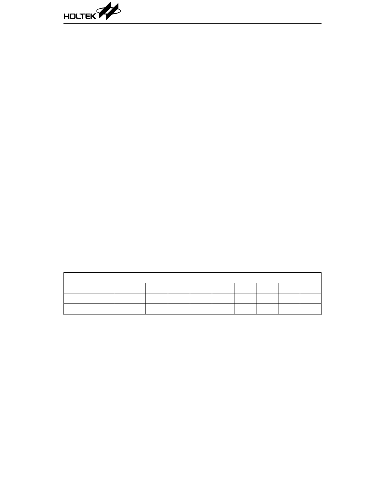
Selection Table
Mask version
Part No. HT48C10 HT48C30 HT48C50 HT48C70
Operating Voltage 2.4V~5.2V 2.4V~5.2V 2.4V~5.2V 2.4V~5.2V
External Interrupt 1 1 1 1
Internal Interrupt 1 1 2 2
8-bit Timer/Event Counter 1 1 1 0
16-bit Timer/Event Counter 0 0 1 2
System Oscillator Crystal/RC Crystal/RC Crystal/RC Crystal/RC
Watchdog Timer 1 1 1 1
ROM 1K
RAM
I/O Lines 18 22 32 56
Instructions 63 63 63 63
Stack Levels 2 2 4 8
Operating Frequency 400kHz~8MHz 400kHz~8MHz 400kHz~8MHz 400kHz~8MHz
Power Down Mode
Table Read Instructions √√ √ √
×14 2K×14 4K×15 8K×16
×8
64
(40H~7FH)
√√ √ √
96×8
(20H~7FH)
160×8
(60H~FFH)
224×8
(20H~FFH)
OTP version
Part No. V
DD
f
SYS
I/O Pull-high Mask version
HT48R11 3.0V~5.2V 400k~4MHz No HT48C10
HT48R12 3.0V~5.2V 400k~4MHz Yes HT48C10
HT48R31 3.0V~5.2V 400k~4MHz No HT48C30
HT48R32 3.0V~5.2V 400k~4MHz Yes HT48C30
HT48R50 3.0V~5.2V 400k~4MHz Yes HT48C50
HT48R51* 3.0V~5.2V 400k~4MHz No HT48C50
* Under development
2 25th May ’99
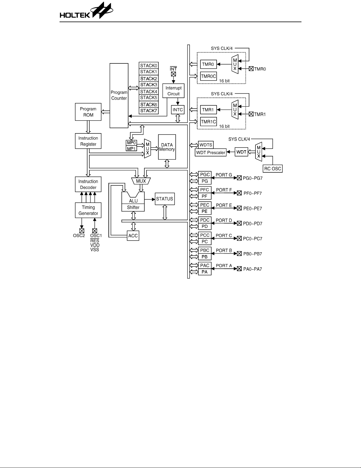
Block Diagram of HT48C70
HT48CXX/HT48RXX
3 25th May ’99
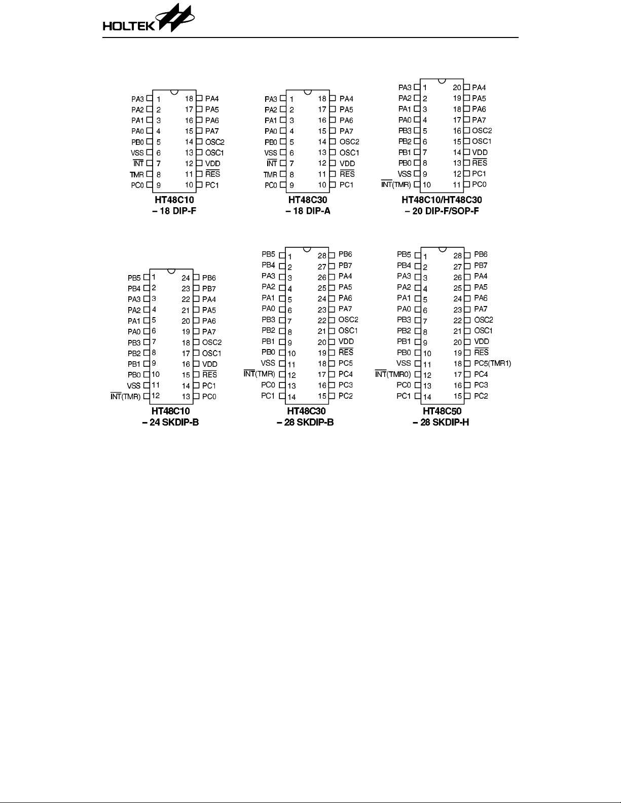
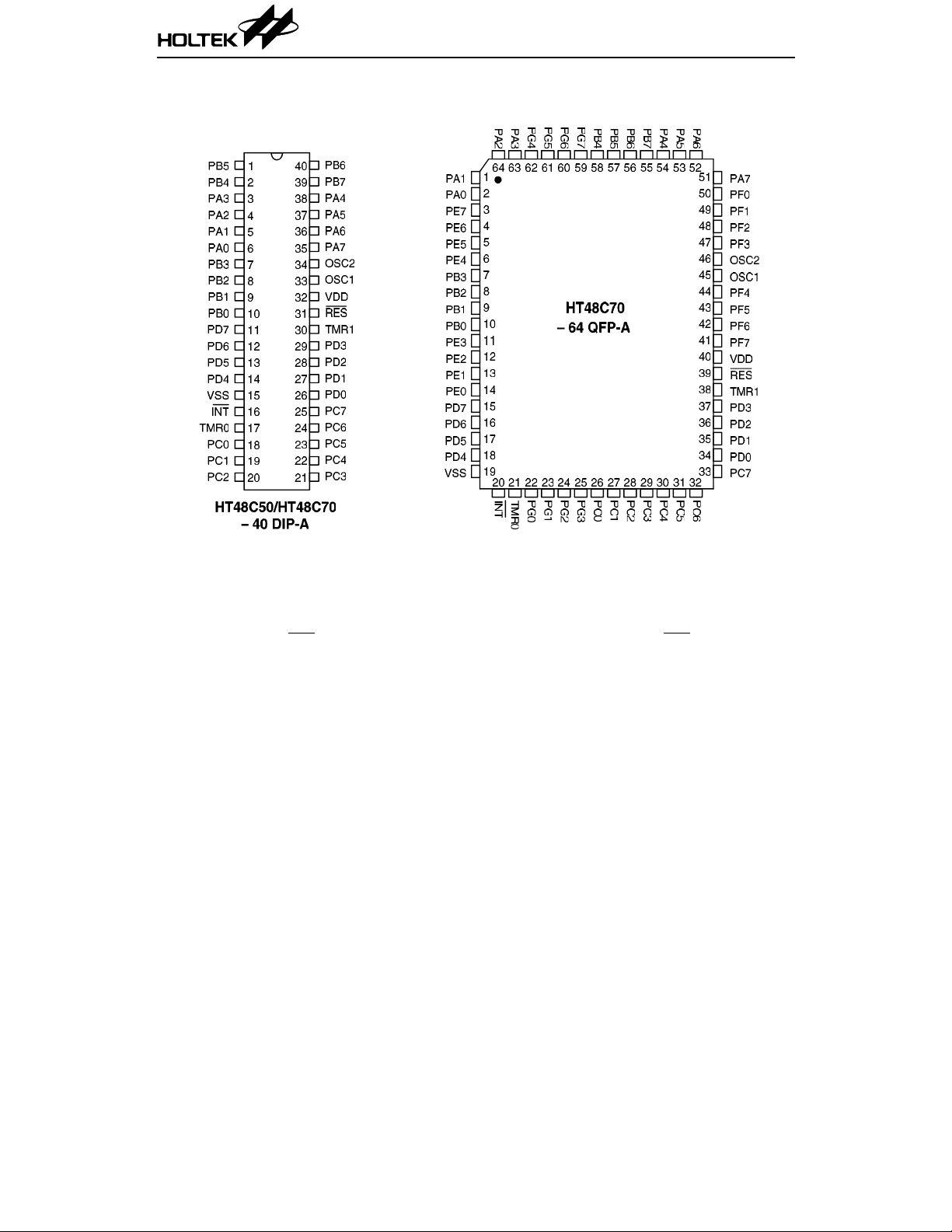
Pin Assignment
HT48CXX/HT48RXX
4 25th May ’99
HT48CXX/HT48RXX
Note: For the dice form, the TMR0 and TMR1 pads have to be bonded to VDD or VSS if t he TMR0
and/or TMR1 pad are not used.
The (TMR0)
The PC5 (TMR1) indicates that the TMR1 pad should be bonded to the PC5 pin.
INT indicates that the TMR0 pad should be bonded to the INT pin.
5 25th May ’99

Pin Description of HT48C10
HT48CXX/HT48RXX
Pin Name I/O
PA0~PA7 I/O
PB0~PB7 I/O
VSS — — Negative power supply, GND
INT I —
TMR I — Schmitt trigger input for timer/event counter
PC0~PC1 I/O
RES I — Schmitt trigger reset input, active low
VDD — — Positive power supply
OSC1
OSC2
I
O
Mask
Option
Wake-up
Pull-high
or None
Pull-high
or None
Pull-high
or None
Crystal or
RC
Function
Bidirectional 8-bit input/output ports
Each bit can be configured as a wake-up input by mask option.
Software instructions determi ne the CMOS output or schmitt
trigger input with or without pull high resistor ( by mask option) .
Bidirectional 8-bit input/output ports
Software instructions determine the CMOS output or schmitt
trigger input with or without pull high resistor (by mask
option).
External interrupt schmitt trigger in put with pull hig h resist or
Edge trigger is activated dur ing hig h to low transition.
Bidirectional 2-bit input/output ports
Software instructions determine the CMOS output or schmitt
trigger input with or without pull high resistor (by mask option) .
OSC1 and OSC2 are con nected to an R C network or a crystal
(by mask option) for the internal system clock. In the case of RC
operation, OSC2 is the output terminal for 1/4 system clock.
6 25th May ’99

Pin Description of HT48C30
HT48CXX/HT48RXX
Pin Name I/O
PA0~PA7 I/O
PB0~PB7 I/O
VSS — — Negative power supply, GND
INT I —
TMR I — Schmitt trigger input for timer/event counter
PC0~PC5 I/O
RES I — Schmitt trigger reset input, active low
VDD — — Positive power supply
OSC1
OSC2
I
O
Mask
Option
Wake-up
Pull-high
or None
Pull-high
or None
Pull-high
or None
Crystal or
RC
Function
Bidirectional 8-bit input/output ports
Each bit can be configured as a wake-up input by mask option.
Software instructions determi ne the CMOS output or schmitt
trigger input with or without a pull high resistor ( by mask option).
Bidirectional 8-bit input/output ports
Software instructions determine the CMOS output or schmitt
trigger input with or without a pull high resistor (by mask
option).
External interrupt schmitt trigger input with a pull high
resistor. Edge triggered is activated on a high to low transition.
Bidirectional 6-bit input/output ports
Software instructions determine the CMOS output or schmitt
trigger input with or without a pull high resistor (by mask
option).
OSC1 and OSC2 are con nected to an R C network or a crystal
(by mask option) for the internal system clock. In the case of RC
operation, OSC2 is the output terminal for 1/4 system clock.
7 25th May ’99

Pin Description of HT48C50
HT48CXX/HT48RXX
Pin Name I/O
PA0~PA7 I/O
PB0~PB7 I/O
VSS — — Negative power supply, GND
INT I —
TMR0 I — Schmitt trigger input for timer/event counter 0
TMR1 I — Schmitt trigger input for timer/event counter 1
PC0~PC7 I/O
RES I — Schmitt trigger reset input, active low
VDD — — Positive power supply
OSC1
OSC2
PD0~PD7 I/O
I
O
Mask
Option
Wake-up
Pull-high
or None
Pull-high
or None
Pull-high
or None
Crystal or
RC
Pull-high
or None
Function
Bidirectional 8-bit input/output ports
Each bit can be configured as a wake-up input by mask option.
Software instructions determi ne the CMOS output or schmitt
trigger input with or without a pull high resistor ( by mask option).
Bidirectional 8-bit input/output ports
Software instructions determine the CMOS output or schmitt
trigger input with or without a pull high resistor (by mask
option).
External interrupt schmitt trigger input with a pull high
resistor. Edge triggered is activated on a high to low transition.
Bidirectional 8-bit input/output ports
Software instructions determine the CMOS output or schmitt
trigger input with or without a pull high resistor (by mask
option).
OSC1 and OSC2 are con nected to an R C network or a crystal
(by mask option) for the internal system clock. In the case of RC
operation, OSC2 is the output terminal for 1/4 system clock.
Bidirectional 8-bit Input/Output port. Software instructions
determine the CMOS output or schm itt trigger input with or
without a pull high resistor (by mask option).
8 25th May ’99

Pin Description of HT48C70
HT48CXX/HT48RXX
Pin Name I/O
PA0~PA7 I/O
PB0~PB7 I/O
VSS — — Negative power supply, GND
INT I —
TMR0 I — Schmitt trigger input for timer/event counter 0
TMR1 I — Schmitt trigger input for timer/event counter 1
PC0~PC7 I/O
RES I — Schmitt trigger reset input, active low
VDD — — Positive power supply
OSC1
OSC2
PD0~PD7 I/O
PE0~PE7 I/O
PF0~PF7 I/O
PG0~PG7 I/O
I
O
Mask
Option
Wake-up
Pull-high
or None
Pull-high
or None
Pull-high
or None
Crystal or
RC
Pull-high
or None
Pull-high
or None
Pull-high
or None
Pull-high
or None
Function
Bidirectional 8-bit input/output ports
Each bit can be configured as a wake-up input by mask option.
Software instructions determi ne the CMOS output or schmitt
trigger input with or without pull high resistor ( by mask option) .
Bidirectional 8-bit input/output ports
Software instructions determine the CMOS output or schmitt
trigger input (pull-high depends on mask option).
External interrupt schmitt trigger with pull high resistor
Edge trigger is activated during high to low transition.
Bidirectional 8-bit input/output ports
Software instructions determine the CMOS output or schmitt
trigger input (pull-high depends on mask option).
OSC1 and OSC2 are con nected to an R C network or a crystal
(by mask option) for the internal system clock. In the case of RC
operation, OSC2 is the output terminal for 1/4 system clock.
Bidirectional 8-bit input/output ports
Software instructions determine the CMOS output or schmitt
trigger input (pull-high depends on mask option).
Bidirectional 8-bit input/output ports
Software instructions determine the CMOS output or schmitt
trigger input (pull-high depends on mask option).
Bidirectional 8-bit input/output ports
Software instructions determine the CMOS output or schmitt
trigger input (pull-high depends on mask option).
Bidirectional 8-bit input/output ports
Software instructions determine the CMOS output or schmitt
trigger input (pull-high depends on mask option).
9 25th May ’99
HT48CXX/HT48RXX
Absolu te Maxim um Ratings
Supply Voltage .......................VDD–0.3V to 5.5V Storage Temperature.................–50°C to 125°C
Input Voltag e .... ........ .....V
Note: These are stress ratings only. Stresses exceeding the range spe cified under “Absolute Maxi -
mum Ratings” may cause substantial damage to the device. Functional operation of this device
at other conditions beyond those listed in the specification is not implied and prolonged
exposure to extreme condition s may affect device reliability.
D.C. Characteristics Ta=25°C
–0.3V to VDD+0.3V Operating Temperature ..............–25°C to 70°C
SS
Symbol Parameter
V
I
DD1
I
DD2
I
DD3
I
DD4
I
DD5
I
DD6
I
DD7
I
DD8
I
STB1
I
STB2
DD
Operating Voltage — — 2.4 — 5.2 V
Operating Current
(HT48C10 Crystal OSC)
Operating Current
(HT48C10 RC OSC)
Operating Current
(HT48C30 Crystal OSC)
Operating Current
(HT48C30 RC OSC)
Operating Current
(HT48C50 Crystal OSC)
Operating Current
(HT48C50 RC OSC)
Operating Current
(HT48C70 Crystal OSC)
Operating Current
(HT48C70 RC OSC)
Standby Current
(WDT Enabled)
Standby Current
(WDT Disabled)
Test Conditions
V
3V
5V — 2 3
3V
5V — 1 2
3V
5V — 2 3
3V
5V — 1 2
3V
5V — 2.5 5
3V
5V — 1.5 3
3V
5V — 3.4 6
3V
5V — 2.1 4
3V
5V — — 10
3V
5V — — 2
DD
Conditions
No load
f
=4MHz
SYS
No load
f
=2MHz
SYS
No load
f
=4MHz
SYS
No load
f
=2MHz
SYS
No load
f
=4MHz
SYS
No load
f
=2MHz
SYS
No load
f
=4MHz
SYS
No load
f
=2MHz
SYS
No load
system halt
No load
system halt
Min. Typ. Max. Unit
—0.71.5
—0.5 1
—0.71.5
—0.5 1
—1 2
— 0.75 1.5
—1.5 3
—1 2
—— 5
—— 1
mA
mA
mA
mA
mA
mA
mA
mA
µA
µA
10 25th May ’99
HT48CXX/HT48RXX
Symbol Parameter
V
IL
V
IH
V
IL1
V
IH1
V
IL2
V
IH2
I
OL
I
OH
R
PH
Input Low Voltage for I/ O
ports
Input High Voltage for I/O
Ports
Input Low Voltage
(
TMR, TMR0, TMR1, INT)
Input High Voltage
(
TMR, TMR0, TMR1, INT)
Input Low Voltage (RES)
Input High Voltage (RES)
I/O Ports Sink Current
I/O Ports Source Current
Pull-high Resistance of I/O
Ports and
INT
Test Conditions
V
DD
Conditions
Min. Typ. Max. Unit
3V — 0 — 0.9
5V — 0 — 1.5
3V — 2.1 — 3
5V — 3.5 — 5
3V — 0 — 0.7
5V — 0 — 1.3
3V — 2.3 — 3
5V — 3.8 — 5
3V — — 1.5 —
5V — — 2.5 —
3V — — 2.4 —
5V — — 4.0 —
3V V
5V V
3V V
5V V
=0.3V 1.5 4 —
OL
=0.5V 4 10 —
OL
=2.7V –1 –2 —
OH
=4.5V –2 –4.5 —
OH
3V — 40 60 80
5V — 10 30 50
V
V
V
V
V
V
mA
mA
k
Ω
11 25th May ’99

HT48CXX/HT48RXX
A.C. Characteristics Ta=25°C
Symbol Parameter
f
SYS1
f
SYS2
f
TIMER
t
WDTOSC
t
WDT1
t
WDT2
t
RES
t
SST
t
INT
System Clock (Crystal OSC)
System Clock (RC OSC)
Timer I/P Frequency
(TMR, TMR0, TMR1)
Watchdog Oscillator — —
Watchdog Time-out
Period (RC)
Watchdog Time-out Period
(System Clock)
External Reset Low Pulse
Width
System Start-up Timer
Period
Interrupt Pulse Width — — 1 — — µs
Test Conditions
V
DD
Conditions
Min. Typ. Max. Unit
3V — 400 — 4000 kHz
5V — 400 — 8000 kHz
3V — 400 — 2000 kHz
5V — 400 — 3000 kHz
3V — 0 — 4000 kHz
5V — 0 — 4000 kHz
45 90 180
µs
35 65 130
Without WDT
—
prescaler
Without WDT
—
prescaler
—— 1——
12 23 45
ms
91735
—1024— t
SYS
µs
Power-up or
—
Wake-up from
—1024— t
SYS
halt
Note: t
SYS
=1/f
SYS
12 25th May ’99
Functional Description
The four microcontrollers of the HT48C10/
HT48C30/HT48C50/HT48C70 are constructed
using basically the same principles. Their differences lie in variati ons in sizes su ch as ROM
and RAM as wel l as bit num ber, counter number , I/O line number , and different level subroutine nesting bit number. The following is a more
detailed description of the system architectures
of the four microcontrollers. Unless specified,
the architecture stated below exists in these
four microcontrollers.
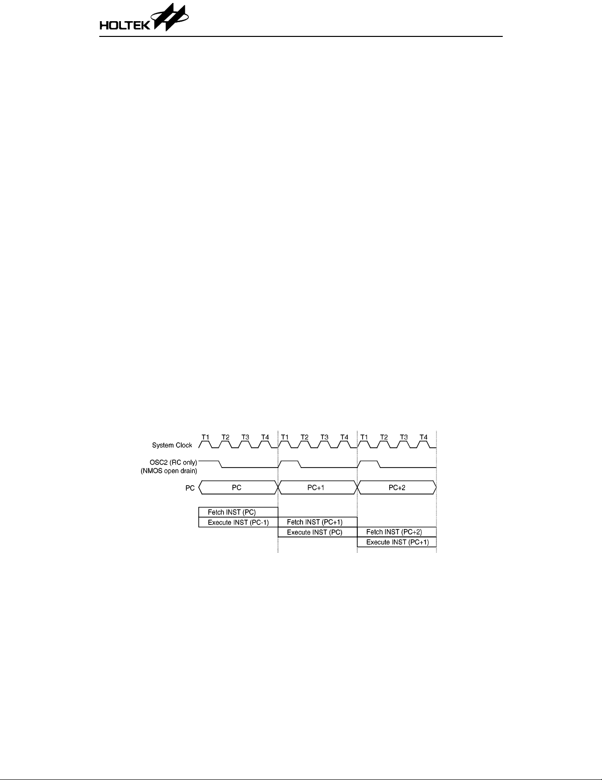
Execution flow
The system clock is derived from either a crystal
or an RC oscillator. It is internally divided into
four non-overlapping clocks. Each instruction
cycle consists of four system clock cycles.
Instruction fetching and execution are pipelined in such a way that a fetch takes one i nstruction cycle while decoding and execution
takes the next instruction cycle. The pipelining
scheme causes each instruction to effectively
execute in a cycle. If an instruction changes the
program counter, two cycles are required to
complete the instruction.
Program counter – PC
The program counter (PC) is of different sizes
ranging from 10 b its to 1 3 b its acco rdin g to the
microcontroller selected (10 bits for the
HT48C10; 11 bits for the HT 48C30; 12 bits for
the HT48C50; 13 bits for the HT48C70). It con-
HT48CXX/HT48RXX
trols a sequence in which the instructions
stored in the program ROM are executed . The
contents of the PC can specify 1024, 2048, 4096,
or 8192 addresses at maximum, according to
the microcontroller (HT48C10/HT48C30/
HT48C50/HT48C70) chosen.
After accessing a program memory word i n order to fetch an instruction code, the contents of
the PC is incremented by one. The PC then
points to the memory word consisting of the
next instruction code.
When executing a jump instruction, conditional
skip execution, loa ding a PCL register, a subroutine call, an initia l reset, an internal interrupt, an external interrupt, or returning from a
subroutine, the PC manipulates a program
transfer by loading the addres s corresponding
to each instruction.
The conditional skip is activated by inst ructions.
Once the condition is met, the next instruction,
fetched during the current instruction execution,
is discarded and a dummy cycle replaces it to get
a proper instruction; otherwise it proceeds to the
next instruction.
The lower byte of the PC (PCL) is a readable
and writeable register (06H). Moving data into
the PCL performs a short jump. The destination
is within 256 locations.
For a control transfer to take place, an additional dummy cycle is required.
Execution flow
13 25th May ’99
Progr a m me mory – ROM
The program memory (ROM) is used to store the
program instructions that are to be executed. It
contains data, table, and interrupt entries, and
is organized into 1024
4096
×15 bits, or 8192×16 bits according to the mi-
×14 bits, 2048×14 bits,
crocontroller (HT48C10/ HT48C30/HT48C50/
HT48C70) selected. These bits are all addressed by the
PC and table pointer .
Certain locations in the ROM s tated belo w are
reserved for special usage in the four microcontrollers except loca tion 00C H which is used for
the HT48C50/HT48C70 exclusively.
•
Location 000H
Location 000H is reserved for program in-
itialization. After chip reset, the progra m always begins execution at this area.
•
Location 004H
Location 004H is reserved for external inter-
rupt service program. If the
INT input pin is
activated, the interrupt is enabled, and the
stack is not full, the program begins execution
at location 004H.
•
Location 008H
Location 008H is reserved for the timer/event
counter interrupt service program of the
HT48C10/HT48C30 and for the timer/event
counter 0 interrupt service program of the
HT48CXX/HT48RXX
Program memory
HT48C50/HT48C70. If the timer interrupt results from a timer/even t counter overflow of
the HT48C10/HT48C30 or a timer/event
counter 0 overflow of the HT48C50/HT48C70,
and the interrupt is enabled, and the stack is
not full, the program begins execution at location 008H.
Mode Contents of Program Counter (m bits)
Initial reset 0000H
External interrupt 0004H
Timer/event counter 0 overflow 0 008H
Timer/event counter 1 overflow 0 00CH
Skip PC+2
Loading PCL Low byte replaced by instruction code
Jump, call branch Instruction code
Return from subroutine Stack register
Notes: m=10 for the HT48C10
m=11 for the HT48C30
m=12 for the HT48C50
m=13 for the HT48C70
14 25th May ’99
HT48CXX/HT48RXX
•
Location 00CH
Location 00CH is reserved for the timer/ event
counter 1 interrupt service program of the
HT48C50/HT48C70 only. If the timer interrupt results from a timer/event counter 1
overflow, the interrupt is enabled, and the
stack is not full, the program begins execution
at location 00CH.
•
Table locati on
Any location in the ROM can be used as a
look–up table. The instructio ns TABRDC [m]
(the current page, 1 page=256 words) and
TABRDL [m] (the last page) transfer the contents of the lower-order byte to the sp ecified
data memory, and the higher-order byte to
TBLH (08H). Only the destination of the
lower-order byte in the table is well-defin ed,
and the higher-order byte of the table word is
transferred to the Table Higher-order byte
register (TBLH). Th e TB LH i s read only. The
Table Pointer (TBLP), on the other hand, is a
read/write register (07H) used to indi cate the
table location. B efore a ccessing th e tab le, the
location should be placed in the TBLP. The
TBLH is read only and canno t be restore d. If
the main routine and the ISR (Interrupt Service Routine) both employ the table read instruction, the contents of the TBLH in the
main routine is likely to be changed by the
table read instruction used in the ISR. Errors
will then occur. Hence, simultaneously using
the table read instruction in the main routine
and the ISR should be avoided. Nonetheless,
if the application of the table read instruction
to both the main routin e and the ISR cannot
be avoided, interrupts should be disabled
prior to the table read instruction, and they
should not be enabled until the TBLH is
backed-up. All the table related instructions
require 2 cycles to complete an operation.
These areas may function as a normal program memory depend ing upon the user ’s requirements.
Stack register – STACK
The stack register is a special memory port used
to save the contents of the PC. The stack can be
organized into 2, 4, o r 8 levels according to the
microcontroller selected (2 levels for the
HT48C10/HT48C30, 4 levels for the HT48C50,
8 levels for the HT 48C70). The registe r is neither part of the da ta nor part of the program,
and is neither readable nor writeable. Any activated level is indexed by a stack pointer (SP)
and is neither readable nor writeable. At a subroutine call or inte rrupt acknowledgment , the
contents of the PC is pushe d o nto the sta ck. At
the end of a subroutine or an interrupt routine,
signaled by a return instruction (RET or RETI),
the contents of the PC is restored to its previous
value from the stack. After chip reset, the SP
will point to the top of the stack.
If the stack is full and a non-masked interrupt
takes place, the interrupt request fl ag is record ed
but the acknowledgment is still inhibited. After
the stack pointer is decremented (by RET or
RETI), the interrupt will be serviced. This feature
prevents the occurrence of stack overflow, allow-
Instruction(s)
*m~*8
∗7 ∗6 ∗5 ∗4 ∗3 ∗2 ∗1 ∗0
Ta ble Loc ation
TABRDC [m] Pm~P8 @7 @6 @5 @4 @3 @2 @1 @0
TABRDL [m] 1~1 @7 @6 @5 @4 @3 @2 @1 @0
Table locati on
Notes:
∗m~∗0: Bits of table location
@7~@0: Bits of table pointer
Pm~P8: Bits of current
Program Counter
15 25th May ’99
m=9 for the HT48C10
m=10 for the HT48C30
m=11 for the HT48C50
m=12 for the HT48C70
ing the programmer to use the structure easily.
Likewise, if the stack is full and a CALL is
subsequently executed, a stack overflow will
occur and the first entry will be lost (only the
most recent four return addresses will be
stored).
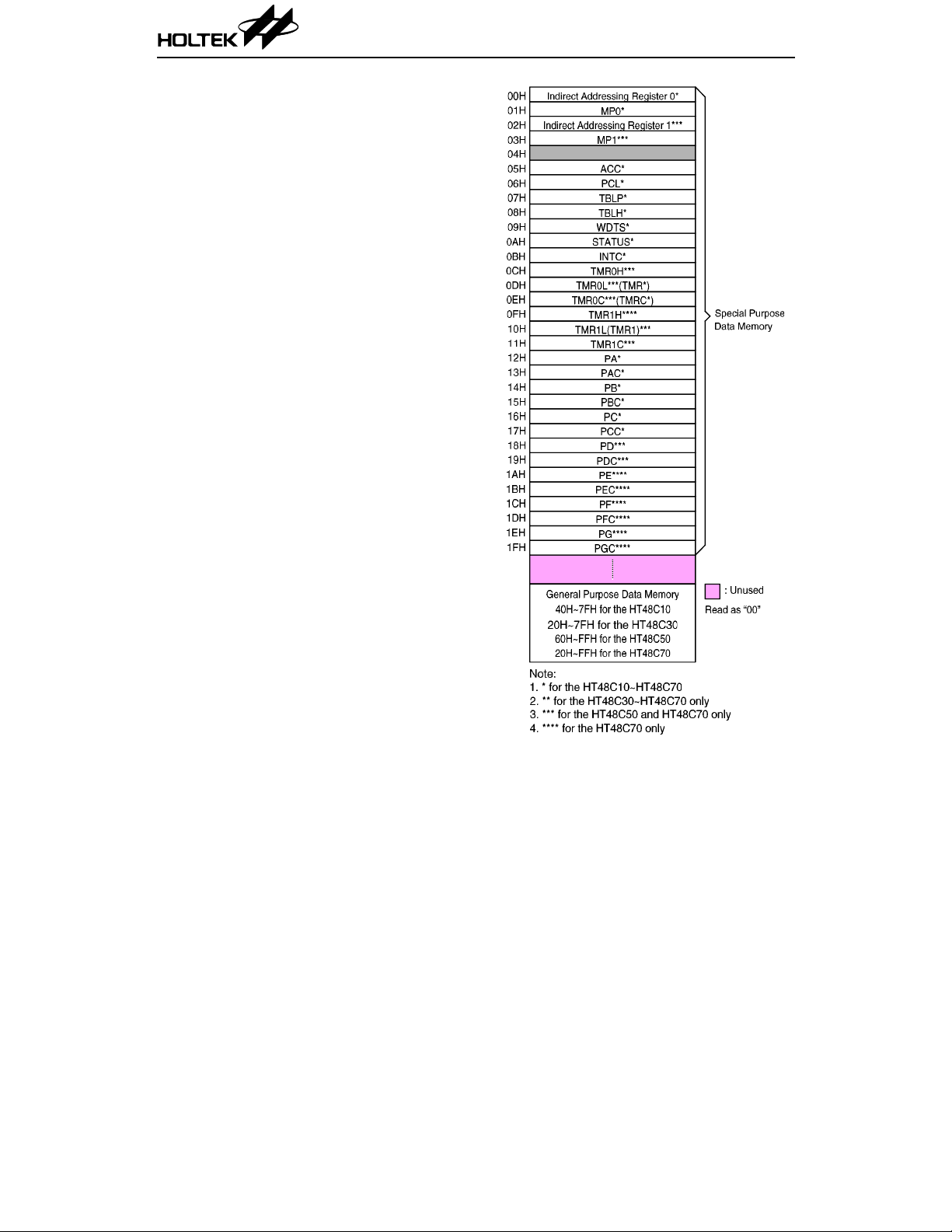
Data memory – RAM
The data memory (RAM) is composed of bits
ranging from 8 1
pending on the microcontroller chosen
(HT48C10/ HT48C30/HT48C50/HT48C70). It is
divided into two function al groups, i.e., special
function registers and general purpose data
memory (of 64
depending on the microcontroller selected
(HT48C10/ HT48C30/HT48C50/HT48C70).
Most components of the two functional groups
are readable/writable, but some are read-only.
Of the two functional groups , the special function registers of the four mi crocontrollers consist of a program counter lower-order byte
register (PCL;06H), an accumulator (ACC;
05H), a table pointer (TBLP;07H), a table
higher-order byte register (TBLH;08H), a
status register (STATUS;0AH), an interrupt
control register (INT C;0BH), a wa tchdo g timer
option setting register (WDTS;09H), an indirect
addressing register (00H), a memory pointer
register (MP;01H), a timer/event counter
(TMR;0DH), a timer/event counter control register (TMRC;0EH), I/O registers
(P A;12H,PB;14H, PC;16H), and I/O control registers (PAC;13H,PBC;15H,PCC;17H). But of
the HT48C50/HT48C70, the following components are further divided into two or several
sub-components. First, the indirect addressing
register is divided into two registe rs involving
indirect addressing register 0 (00H) and ind irect addressing register 1 (02H). Second, the
memory pointer register is also comprised by
two registers involving memory pointer register
0 (MP0;01H) and memory pointer register 1
(MP1;03H). Third, the timer/event counter register is organized by two registe rs according to
different orders of byte, namely timer/event
higher-order byte register and timer/event
lower-order byte register, both of which are further divided into timer/event counter 0 higher-
×8, 113×8, 184×8, or 255×8, de-
×8, 96×8, 160×8, or 224×8 bits,
HT48CXX/HT48RXX
RAM mapping
order byte register (TMR0H; 0CH), timer/ event
counter 1 higher-order byte register
(TMR1H;0FH), timer/event counter 0 lowe r-order byte register (TMR0L;0DH), and
timer/event counter 1 lowe r-order byte regi ste r
(TMR1L;10H). Fourth, the timer/eve nt counte r
control register is divided into two registers
involving timer/event counter 0 control register
16 25th May ’99

HT48CXX/HT48RXX
(TMR0C;0EH) and timer/event counter 1 control register (TMR1C;11H). Fifth, the entire
number of I/O registers is expanded from 3 to 6
(PA;12H,PB;14H,PC;16H,PD;18H,PE;1AH,
PF;1CH,PG; 1EH). Finally, the number of I/O
control registers is also doubled (PAC;13H,
PBC;15H,PCC;17H,PDC;19H,PEC;1BH,
PFC;1DH,PGC;1FH). The remaining space before the 20H of the four microcontrollers are all
reserved for future expansion usage. Reading
these remaining locations will return the result
to 00H. The general purpose data memory, addressed from 40H~7FH of the HT48C10,
20H~7FH of the HT48C30, 60H~FFH of the
HT48C50, or 20H~FFH of the HT48C70 according to the microcon troller selected, is used for
data and control information under instruction
commands.
All the RAM areas can directly execute arithmetic, logic, increment, decrem ent, and rotate operations. Except some dedicated bits, each bit in
the RAM can be set and reset by the SET [m].i
and CLR [m].i instructi ons, res pectivel y. These
RAM areas are indirectly accessible through the
memory pointer register(s) MP (01H) of the
HT48C10/HT48C30 or MP0 (01H) and MP1
(03H) of the HT48C50/HT48C70.
Indirect addressing register
Of the four microcontrollers, the HT48C10/
HT48C30 make use of location 00H whereas the
HT48C50/HT48C70 of locations 00H and 02H
as indirect addressing registers that are not
physically imple mente d. An y rea d/write ope ration of [00H] or of [00H] and [02H] accesses the
RAM pointed to by MP (01H) or by MP0 (01H)
and MP1 (03H) respectively according to the
microcontroller chosen. Reading location 00H or
02H indirectly will return the result 00H. Writing it indirectly will, result to no operation.
The function of data movement between two
indirect addre ssing registers is not suppo rted.
The memory pointer register MP of the
HT48C10/HT48C30 or MP0 and MP1 of the
HT48C50/HT48C70 are of 7 bits or 8 bits wide
respectively , and can be used to access the RAM
by combining the corresponding indirect addressing registers. The bit 7 of MP
(HT48C10/HT48C30) is undefined and reading
will return the result “1”. Any writing operation to
MP will only transfer the lower 7-bit data to MP.
Accumulator ACC
The accumulator (AC C) relate s to the ALU o perations. It is also mapped to location 05H of the
RAM and is capable of operating with immedi ate data. The data movement between two data
memories will pass through the ACC.
Arithmetic and logic unit – ALU
This circuit performs 8-bit ari thm eti c and lo gic
operations. It provides the following functions:
•
Arithmetic operations (ADD, ADC, SUB,
SBC, DAA)
•
Logic operations (AND, OR, XOR, CPL)
•
Rotation (RL, RR, RLC, RRC)
•
Increment and Decrement (INC, DEC)
•
Branch decision (SZ, SNZ, SIZ, SDZ, etc.)
The ALU saves the results of the data operation
and change the status register as well.
Status register – STATUS
The status registe r (0AH) i s of 8 bits wi de and
consists of a zero flag (Z), a carry flag (C), an
auxiliary carry flag (AC), an overflow flag (OV),
a power down flag (PD) , and a watchdog ti meout flag (TO). The register also records the status
information and controls the operation sequence.
Except the TO and PD flags, bits in the status
register can all be altered by instructions, similar to the case with other registers. A ny data
written into the status regi ste r wil l n ot ch ange
the TO or PD flags. But the opera tions related
to the status register m ay lead to different results from t hose int ended. The TO an d PD flag s
can be changed by system power up, Watchdog
Timer overflow, executing the HALT instruction, or clearing the W atchdog Timer . The Z, OV ,
AC, and C flags all reflect the status of the
latest operations.
17 25th May ’99

HT48CXX/HT48RXX
On entering the interrupt sequence or executing the subroutine call, the sta tus registe r will
not be automati cally pu shed o nto the sta ck . If
the contents of the statu s is impo rtant an d the
subroutine can corrup t the status register, the
programmer should take preca ution s to save it
properly.
Inte r r upt
The four microcon trollers all provide a n external interrupt and internal time r/event counte r
interrupts. The interrupt control register
(INTC;0BH) contains interrupt control bits for
setting the enable/disable mode and the interrupt
request flags.
Once an interrupt subroutine is serviced, the
remaining interrupts will all be blocked (by
clearing the EMI bit). This scheme may prevent
any further interrupt nesting. Other interrupt
requests may happen during this interval but
only the interrupt request flag will be recorded.
If a certain interrupt requires servicing within
the service routine, the progr ammer may set the
EMI bit and the corresponding bit of INTC so as
to allow interrupt nesting. If the st ack is full, the
interrupt request will not be acknowledged, even
if the related interrupt is enabled, until the SP
is decremented. If immediate servicing is desired, the stack should be prevented from becoming full.
All these interrupts have a wake-up cap abilit y.
As an interrupt is serviced, a control transfe r
occurs by pushing the PC on to the stack and
then by branching it to subroutines at the specified location(s) in the ROM. Only the contents of
the PC can be pushed onto the stack. If the
contents of the register an d of the statu s register (STATUS) are altered by the interrupt service program which corrupts the desire d control
sequence, the programmer should save these
contents first.
The external interrupt is triggered by a high to
low transition of the
rupt request flag ( EIF; bit 4 of INTC) is then set.
When the interrup t is e nabled , the stack is not
full, and the external interrupt is active, a subroutine call to location 04H will occur. The interrupt request flag (EIF) and EMI bits will also be
cleared to disable other interrupts.
Of the four microcontrollers, the internal
timer/event counter interrupt of the HT48C1 0/
HT48C30 is initialized by setting the timer/
Labels Bits Function
C is set if the o peration res ults in a carry during an addition opera tion or if a
C0
AC 1
Z2
OV 3
PD 4
TO 5
— 6 Undefined, read as 0
— 7 Undefined, read as 0
borrow does not take place during a subtraction operation; otherwise C is
cleared. Also it is affected by a rotate through carry instruction.
AC is set if the operation results in a carry out of the low nibbles in addition or
no borrow from the high nibble into the low nibble in subtraction; otherwise AC
is cleared.
Z is set if the result of a n arithmetic or logic operati on is zero; otherwise Z is
cleared.
OV is set if the opera tion res ults in a carry into the highe st-order bit but not a
carry out of the highest-order bit, or vice versa; otherwise OV is cleared.
PD is cleared by either a system power-up or executing the CLR WDT
instruction. PD is set by executing the HALT instruction.
TO is cleared by a system power-up or executing the CLR WDT or HALT
instruction. TO is set by a WDT time-out.
INT, and the related inter-
Status register
18 25th May ’99

HT48CXX/HT48RXX
event counter interrupt request flag (TF; bit 5 of
INTC), that is caused by a timer overflow. When
the interrupt is enable d, and the stack is not
full, and the TF bit is set, a subroutine call to
location 08H will occur. The related interrupt
request flag (TF) will b e reset and the EMI bit
will be cleared to disable further interrupts.
The internal timer/event counter of the
HT48C50/HT48C70, is composed of two interrupts, namely internal timer/event counter 0
interrupt and time r/event counter 1 i nterrupt.
The internal timer/event cou nter 0 inte rrupt is
initialized by setting the timer/event counte r 0
interrupt request flag (T0F; bit 5 of INTC)
which is caused by a timer/event counter 0 overflow. After the interrupt is enabled, the stack is
not full, and the T0F bit is set, a subroutine call
to location 08H will occur. The related interrupt
request flag (T0F) will be reset and the EMI bit
be cleared to disable further interrupts. On the
other hand, the timer/event counter 1 interrupt
is operated in the same mann er as the timer/
event counter 0. The related inte rrupt control
bits ET1I and T1F of the timer/eve nt cou nte r 1
are bit 3 and bit 6 of the INTC, respectively.
During the execution of an interr upt subr outine
of the four microcontrollers, other interrupt ac-
knowledgments are all held until the RETI instruction is executed or the EMI bit and the
related interrupt control bit are both set to 1
(when the stack is not full). To return from the
interrupt subroutine, the RET or RETI instruction may be invoked. The RETI will set the EMI
bit in order to enable an interrupt service
whereas the RET will not.
Interrupts that occur in an interval between the
rising edges o f two consecutive T2 pulses are
serviced on the latter of the two T2 pulses if the
corresponding interrupts are enabled. In case of
simultaneous requests, the following table
shows the priority that is applied. These can be
masked by resetting the EMI bit.
No. Interrupt Source Priority Vector
a External interrupt 1 04H
Timer/event
b
counter 0 overflow
Timer/event
*c
counter 1 overflow
* Note: c applies only to the HT48C50/ HT48C70
208H
30CH
Register Bit No. Label Function
Control the master (global) interrupt
(1= enable d; 0= d is abled)
Control the external interrupt
(1= enable d; 0= d is abled)
Control the timer/event counter 0 interrupt
(1= enable d; 0= d is abled)
Control the timer/event counter 1 interrupt (for the
HT48C50/HT48C70 only) (1= enabled; 0= disabled)
External interrupt request flag
(1= active; 0= inactive)
Internal timer/event counter 0 request flag
(1= active; 0= inactive)
Internal timer/event counter 1 request flag (for the
HT48C50/HT48C70 only) (1= active; 0= inactive)
INTC register
19 25th May ’99
INTC
(0BH)
0EMI
1
2
3ET1I
4EIF
5
6
7 — Unused bit, read as “0”
EEI
ET0I
T0F
T1F

The timer/even t counter interru pt reque st flag
(TF), external inte rrupt reques t flag (EIF), e nable timer/event counter bit (ETI), enable external interrupt bit (EEI), and enable master
interrupt bit (EMI) constitute an interrupt control register (INTC) of th e HT48C10/HT48C30
which is located at 0BH in the RAM. On the
other hand, the timer/event counter 0/1 interrupt request flag (T0F/T1F), external interru pt
request flag (EIF), e nable timer/event counter
0/1 bit (ET0I/ET1I), enable externa l interrupt
bit (EEI), and enable master interrupt bit (EMI)
make up the interrupt control register (INTC) of
the HT48C50/HT48C70 which is located at 0BH
in the RAM. EMI, EEI, and ETI, of the
HT48C10/HT48C30 or EMI, EEI, ET0I, and
ET1I of the HT4 8C50/HT 48C70 a re all us ed to
control the enable /disable status of interrupts.
These bits prevent the requested interrupt from
being serviced. Once the interrupt request flags
(TF, EIF of the HT48C10/HT48C30 or T0F , T1F,
EIF of the HT48C50/HT48C70) are set, they
will remain in the INTC register until the interrupts are all s erviced or cleared by a software
instruction.
It is suggested that a program should not employ the “CALL subroutine” within the interrupt subroutine, since its operation within the
interrupt subroutine may damage the original
control sequence, and interrupts often occur in
an unpredictable manner or it may need immediate servicing for certain applications. Given
this, if only one stack is left and enabling the
interrupt is not well controlled, the original control sequence may be ruined as a result of operating
the CALL subroutine in the interrupt subroutine.
Oscil lator configuration
There are 2 oscillator circuits available, namely
RC oscillator and crysta l oscillator, decided by
mask options. Both are designed for system
clocks. No matter what type o f oscillator is chosen, the signal supports th e system clock. The
HALT mode stops the system oscillato r and ignores any external signals so as to conserve
power.
Of the two oscillator types, if an RC oscillator is
used, an external resistor between OSC1 and
HT48CXX/HT48RXX
System oscillator
VDD is required and its resistance ranges from
51k
Ω to 1MΩ. The system clock, divided by 4, is
available on OSC2 (NMOS open drain output),
which can be used to synchronize external logic.
The RC oscillator provides the most cost effective solution. However, the frequency of the oscillation may vary with VDD, temperature and
the chip itself due to process variation s. It is,
therefore, not suitabl e for timing sensitive operations where accurate osci llator frequen cy is
desired. On the other ha nd, if the crystal oscillator is used, a crystal across OSC 1 and OSC2
is needed to provide the feedback and phase
shift required for the crystal oscillator. No other
external components are required . Inste ad of a
crystal, the resonator can also be connected between OSC1 and OSC2 to derive a frequency
reference, but two e xternal capa citors in OSC 1
and OSC2 are required.
The WDT oscil lator is a free ru nning o n-chip RC
oscillator, and no external components are required. Even if the system enters the power
down mode, the system clock is stopped but the
WDT oscillator still works with a period of approximately 78
disabled by mask option to conserve power.
Watchdog timer – WDT
The clock source of the WDT is implemented by
a dedicated RC oscillator (WDT oscillator) or an
instruction clock (system clock divided by 4),
decided by mask options. The WDT is designed
to prevent a software malfunction or seque nce
from jumping to an un known loca tion wi th unpredictable re sults. The WDT can be dis abled
by mask option. If the WDT is disabled, all the
executions related to the WDT may lead to no
operation.
µs. The WDT oscillator can be
20 25th May ’99

Watchdog timer
HT48CXX/HT48RXX
If the internal WDT oscillator (RC oscillator
with a period of 78
µs normally) is selected, it is
first divided by 256 (8 stages) to de rive a nom inal time-out perio d of about 20ms. This tim eout period may vary with temperature, VDD,
and process variation s. By invoking the WDT
prescaler, longer time-out periods can be realized. Writing data to WS2, WS1, and WS0 (bit
2,1,0 of the WDTS) can lead to different timeout periods. If the values of WS2, WS1, and WS0
all equal to 1, the di vision ratio is up to 1:128,
and the maximum time-out period is 2.6 seconds.
But if the WDT oscillator is disabled, the WDT
clock may still come from the instructio n clock
and operate in the same ma nner exce pt that in
the HALT state the WDT may stop counting
and lose its protecting purpose. In this situation
the logic can be restarted by external logic. The
high nibble and bit 3 of the WDTS are reserved
for user defined flags, and the programmer may
use these flags to indicate some specified status.
WS2 WS1 WS0 Division Ratio
000 1:1
001 1:2
010 1:4
011 1:8
1 0 0 1:16
1 0 1 1:32
1 1 0 1:64
1 1 1 1:128
WDTS Register
If the device operates in a noisy environme nt,
using the on-chip RC oscillator (WDT OSC) is
strongly recommended, since the HALT will terminate the system clock.
The overflow of WDT under no rmal operation
can initialize “chip res et” and set the statu s bit
TO. But in the HALT mode, the overflow will
initialize a “warm reset”, and only the PC and
SP are reset to zero. To clear the contents of
WDT (the WDT prescaler included), three
methods can be adopted, i.e., exte rnal reset (a
low level to
RES), software instruction(s), and a
HALT instruction. The software instruction(s)
consists of CLR WDT and the other set — CLR
WDT1 and CLR WDT2. Of these two types of
instructions, only one type can be active depending on mask option — “CLR WDT times
selection option”. If the “CLR WDT” is chosen
(i.e., CLRWDT times equal on e), any executi on
of the CLR WDT instruction will clear the WDT.
In the case that the “CLR WDT1” and “CLR
WDT2” are chosen (i.e., CLRWDT times equal
two), these two instructions should be executed
to clear the WDT; otherwise, the WDT may
reset the chip due to time-out.
Power down operation – HALT
The HALT mode is initialized by the HALT
instruction and results in the following.
•
The system oscillator turns off but the WDT
oscillator keeps running (if the WDT oscillator
is selected).
•
The contents of the on–chip RAM and registers remain unchanged.
•
The WDT and WDT prescaler are cleared and
recount (if the WDT clock comes from the
WDT oscillator).
•
All I/O ports maintain their original status.
•
The PD flag is set and the TO flag is cleared.
The system can quit the HALT mode by exter-
21 25th May ’99

nal reset, interrupt, external falling edge signal
on port A, or a WDT overflow. An external reset
may cause device initialization, and the WDT
overflow performs a “warm reset”. Examining the
TO and PD flags, the reason for chip reset is
determined. The PD flag is cleared by system
power-up or executing the CLR WDT instruction,
and is set by executing the HALT instruction. The
TO flag is set if the WDT time-out occurs, and
causes a wake-up that resets the PC and SP only.
The others maintain their original status.
The port A wake-up and interrupt methods can
be considered as a conti nuation of normal execution. Each bit in port A can be independently
selected to wake up th e de vice by mas k option.
Awakening from an I/O port stimulus, the program will resume execution of the next instruction. On the other hand, awakening from an
interrupt, two sequences may happen. If the
related interrupt(s) is disabled or the interrupt(s) is enabled but the stack is ful l, the program will resume execution at the next
instruction. But if the i nterrup t is e nabl ed an d
the stack is not full, the regular inte rrupt response takes place.
When wake-up event(s) occurs, it takes 1024
t
(system clock period) to resume normal
SYS
operation. That is to say, a dummy period is
inserted after the wake -up. If the wake-up results from an interrupt acknowledgment, the
actual interrupt subroutine execution will be
delayed by more than one cycle. But if the wakeup results in the next instruction execution, the
instruction will execute im mediately after the
dummy period is finished. If an interrupt request flag is set to “1” before entering the HALT
mode, the make-up function of the related interrupt will be disabled.
To minimize power consumption, all the I/O
pins should be careful ly mana ged be fore en tering the HALT status.
HT48CXX/HT48RXX
Reset timing chart
Reset circuit
Reset configuration
WDT time-out during the HALT is different
from oth er ch ip re set cond itio ns, fo r it can pe rform a “warm reset” that resets only PC and SP
and leaves th e other circuits at their original
state. Some registers remain unchanged during
any other reset conditions. Most of the registers
are reset to the “initial condition” when the
reset conditions are met. By examining the PD
flag and TO flag, the program distinguishes
between different “chip resets”.
Reset
There are three ways in which reset may occur:
•
RES is reset during normal operation
•
RES is reset during HALT
•
WDT timeout is reset during normal operation
TO PD RESET Conditions
00RES reset during power-up
uu
01
22 25th May ’99
RES reset during normal
operation
RES wake-up HALT

HT48CXX/HT48RXX
TO PD RESET Conditions
1u
1 1 WDT wake-up HALT
Note: “u” means “unchanged”
To guarantee that the system oscillator is
started and stabilized, the SST (System Startup Timer) provides an extra-delay. The extradelay delays 1024 system clock pulses when the
system powers up or awakes from the HALT
state.
When the system power-up occurs, the SST delay is added during the reset period. But when
the reset comes from the
is disabled. Any wake-up from HALT will enable
the SST delay.
The status of the chip reset of the functional
units are as shown.
PC 000H
Interrupt Disabled
Prescaler Cleared
WDT
Timer/event
counter (0/1)
Input/out put port s Input mode
SP
WDT time-out during normal
operation
RES pin, the SST delay
Cleared
After a master reset,
WDT begins counting.
Off
Point to the top of the
stack
Timer /event counter
There are two timer/event counters implemented in the four microcontrollers. Of the four
microcontrollers, the timer/event counter of the
HT48C10/HT48C3 0 con tai ns an 8-bi t progra mmable count-up counter . On the other hand, the
timer/event counter of the HT48C5 0/HT48C70
composes of two counters, namely ti mer/event
counter 0 and timer/event counter 1. The
timer/event counter 0 contains a 16-bit programmable counter, and the timer/event
counter 1 contains an 8-bit programmable
count-up counter of the HT48C50. The
timer/event counters 0 and 1 of the HT48C70
both contain a 16-bit programmable count-up
counter. The source of the clock of the four microcontrollers may come from an external
source or the sys tem clock divid ed by 4. If the
internal instruction clock is applied, only one
reference time-base is ava ilable. The extern al
clock input, on th e other hand, al lows the u ser
to count external events, me asure time intervals or pulse width, or generate an accurate
time base.
Of the HT48C10/HT48C30, there are two registers related to the timer/event counter, i.e.,
TMR ([0DH]) a nd TMRC ([0EH] ). Th ere are two
physical registers mapped to the TMR location.
Writing TMR puts the starting value in the
timer/event counter preload register while
reading TMR gets the contents of the timer/
event counter. The TMRC, on the other hand, is
a timer/event counter control register.
Timer/event counter 0/1
23 25th May ’99

HT48CXX/HT48RXX
The states of the special function registers are summarized in the following table:
Register
TMR1H xxxx xxxx uuuu uuuu uuuu uuuu uuuu uuuu uuuu uuuu
TMR1L xxxx xxxx uuuu uuuu uuuu uuuu uuuu uuuu uuuu uuuu
TMR1C 00-0 1--- 00-0 1--- 00-0 1--- 00-0 1--- uu-u u--TMR0H xxxx xxxx uuuu uuuu uuuu uuuu uuuu uuuu uuuu uuuu
TMR0L xxxx xxxx uuuu uuuu uuuu uuuu uuuu uuuu uuuu uuuu
TMR0C 00-0 1--- 00-0 1--- 00-0 1--- 00-0 1--- uu-u u--PC 000H 000H 000H 000H 000H
MP0 xxxx xxxx uuuu uuuu uuuu uuuu uuuu uuuu uuuu uuuu
MP1 xxxx xxxx uuuu uuuu uuuu uuuu uuuu uuuu uuuu uuuu
ACC xxxx xxxx uuuu uuuu uuuu uuuu uuuu uuuu uuuu uuuu
TBLP xxxx xxxx uuuu uuuu uuuu uuuu uuuu uuuu uuuu uuuu
TBLH xxxx xxxx uuuu uuuu uuuu uuuu uuuu uuuu uuuu uuuu
STATUS --00 xxxx --1u uuuu --uu uuuu --01 uuuu --11 uuuu
INTC -000 0000 -000 0000 -000 0000 -000 0000 -uuu uuuu
WDTS 0000 0111 0000 0111 0000 0111 0000 0111 uuuu uuuu
PA 1111 1111 1111 1111 1111 1111 1111 1111 uuuu uuuu
PAC 1111 1111 1111 1111 1111 1111 1111 1111 uuuu uuuu
PB 1111 1111 1111 1111 1111 1111 1111 1111 uuuu uuuu
PBC 1111 1111 1111 1111 1111 1111 1111 1111 uuuu uuuu
PC 1111 1111 1111 1111 1111 1111 1111 1111 uuuu uuuu
PCC 1111 1111 1111 1111 1111 1111 1111 1111 uuuu uuuu
PD 1111 1111 1111 1111 1111 1111 1111 1111 uuuu uuuu
PDC 1111 1111 1111 1111 1111 1111 1111 1111 uuuu uuuu
PE 1111 1111 1111 1111 1111 1111 1111 1111 uuuu uuuu
PEC 1111 1111 1111 1111 1111 1111 1111 1111 uuuu uuuu
PF 1111 1111 1111 1111 1111 1111 1111 1111 uuuu uuuu
PFC 1111 1111 1111 1111 1111 1111 1111 1111 uuuu uuuu
PG 1111 1111 1111 1111 1111 1111 1111 1111 uuuu uuuu
PGC 1111 1111 1111 1111 1111 1111 1111 1111 uuuu uuuu
Reset
(power on)
WDT time-out
(normal
operation)
RES reset
(normal
operation)
RES reset
(HAL T)
WDT
time-out*
(HALT)
Note: “
∗” means “warm reset”
“u” means “unchanged”
“x” means “unknown”
“–” means “undefined”
The bits of the special function registers are denoted as “–” if they are not defined
in the microcontrollers.
24 25th May ’99

HT48CXX/HT48RXX
Of the HT48C50/HT48C70, the timer/event
counter is comprised by two counters, i.e.,
timer/event counter 0 and timer/eve nt counter
1. There are three registers related to the
timer/event counter 0, namely TMR0H (0CH),
TMR0L (0DH), and TMR0C (0EH). Writing
TMR0L only writes the data into a low byte
buffer, but writing TMR0H writes the data
along with the conten ts of the low byte buffer
into the timer/event cou nter 0 prelo ad register
(16-bit). The timer/event counter 0 preload register is changed by writing the TMR0H operations, and writing TMR0L keeps the timer/
event counter 0 preload register unaltered.
Also, reading the TMR0H latches the TMR0L
into the low byte buffer in order to avoid the
false timi ng prob lem. Then, reading the TMR0L
will return the conten ts of the low byte buffer.
In other words, the low byte of the timer/even t
counter 0 cannot be read directly . Instead it has
to read the TMR0H first in order to make the
low byte contents of th e timer/event counter 0
latched into the buffer. On the other hand, there
are also three registers related to the
timer/event counter 1, namely TMR1H (0FH),
TMR1L (10H), and TMR1C (11H). The timer/
event counter 1 operates in the same manner as
the timer/event counter 0.
The TMR0C is a timer/eve nt counter 0 control
register defining the timer/event counter 0 options. The timer /event counter 1 has th e same
options as the timer/event co unter 0 and is defined by TMR1C.
The timer/event counter control registers of the
four microcontrollers a re all used to defin e the
operation mode, counting enable or disable, and
active edge.
The TM0 and TM1 bits define the operation
mode. The event count mode is used to count
external events, which means that the clock
source comes from a n external pin TMR of the
HT48C10/HT48C30 or TMR0/TMR1 of the
HT48C50/HT48C70. T he timer mod e functions
as a normal timer with the clock source coming
from the instruction clock. The pulse width
measurement mode can be used to count the
high or low level duration of the external signal
TMR of the HT48C10/HT48C30 or TMR0/TMR
1 of the HT48C50/HT48C70. The counting is
based on the instruction clock.
In the event count or timer mode, once the
timer/event counter starts counting, it will count
from the current contents in the timer/event
counter to FFH of the HT48C10/HT48C30/
HT48C50 (TMR1) or to FFFFH of the HT48C50
(TMR0)/HT48C70. If an overflow occurs, the
counter is reloaded from the timer/ event counter
preload register and generates the corresponding
interrupt request flag TF (bit 5 of INTC) of the
HT48C10/HT48C30 or T0F/T1F (bit 5/6 of INTC)
of the HT48C50/ HT48C70 at the same time.
Label Bits Function
— 0~2 Unused bits, read as “0”
TE 3
TON 4
— 5 Unused bits, read as “0”
TM0
TM1
To define TMR0/TMR1 active edge of the timer/event counter
(0= active on low to high; 1= active on high to low)
To enable/disable timer counting
(0= disabled; 1= enabled)
To define the operating mode
01= Event count mode (external clock)
6
10= Timer mode (internal clock)
7
11= Pulse width measurement mode
00= Unused
TMR0C/TMR1C register
25 25th May ’99

HT48CXX/HT48RXX
In the pulse width measurement mode with the
values of the TON and TE bits equal to one, if the
TMR0/ TMR1 has received a transient from low
to high (or high to low; if the TE bit is 0) it will
start counting until the TMR of the
HT48C10/HT48C30 or TMR0/TMR1 of the
HT48C50/ HT48C70 returns to the original level
and resets the TON. The measured result remains in the timer/event counter even if the
activated transient happens again. In other
words, only one cycle measurement can be done.
Until setting the TON, the cycle measurement
will re-function as long as it receives further
transient pulse. In this operation mode, the
timer/event counter starts counting according
not to the logic level but to the transient edges.
In the case of counter overflows, the counter is
reloaded from the timer/event counter preload
register and issues an interrupt request just like
the other two modes.
To enable the counting operation, the timer ON
bit (TON; bit 4 of TMRC of the HT48C10/
HT48C30 or bit 4 of TMR0C/TMR1C of the
HT48C50/HT48C70) should be set to 1. In the
pulse width measurement mode, the TON will
be cleared automatically after the measurement cycle is complete. But in the other two
modes the TON can only be reset by instructions. The overflow of the timer/event counter is
one of the wake-up sources. No matter what the
operation mode is, writing a 0 to ETI of the
HT48C10/HT48C30 or to ET0I/ET1I of the
HT48C50/HT48C70 can disable the corresponding interrupt service.
In the case of time r/event counter OFF condition, writing data to the timer/event counter
preload register also reloads that data to the
timer/event counter. But if the timer/event
counter is turned on, data written to the
timer/event counter is reserved only in the
timer/event counter preload register. The
timer/event counter will go on operating until an overflow occurs.
After the timer/event counter (reading TMR
of the HT48C10/HT48C30 or TMR0H/
TMR1H of the HT48C50/HT48C70) is read,
the clock is blocked to avoid erro rs. As this
may results in a counting error, blocking of
the clock should b e taken into account by the
programmer.
Input/output ports
There are various numbers of bidirecti onal input/output lines in the four microcontrollers.
The HT48C10 includes 18 bidirectional input/output lines, labeled from PA to PC, which
are mapped to the [12H], [14H], or [16H] of the
RAM, respectively. The HT48C30 contains 22
bidirectional input/output lines, labeled from
PA to PC, which are mapped to [12H], [14H], or
[16H], respectively . The HT48C50 consists of 32
Input/output por t s
26 25th May ’99

HT48CXX/HT48RXX
bidirectional input/output lines, labeled from
P A to PD, whic h are mapped to the [12H], [14H],
[16H], or 18H], respectively. Finally, the
HT48C70 contains 56 bidirectional input/output lines, labeled from PA to PG, which are
mapped to the RAM of [12H], [14H], [16H],
[18H], [1AH], [1CH], and [1EH], respectively. Of
the four microcontrol lers, all o f these I/O ports
can be used for input and output operations. For
the input operatio n, these ports are no n-latching, i.e., the inputs should be ready at the T2
rising edge of the instruction MOV A,[m]
(m=12H, 14H, 16H, 18H, 1AH, 1CH, or 1EH).
For the output operati on, all data are latched
and remain unchanged until the output latch is
rewritten.
Each I/O line has its own control register (P AC,
PBC, PCC, PDC, PEC, PFC, PGC (the fist three
registers PAC, PBC, PCC are all used by the
four microcontrollers; the register PDC is extraused by the HT 48C50; all the seven registers
are applied in the HT48C70) to contro l the input/ output configuration. With this control register, CMOS output or schmitt trigger input
with or without pull-high resis tor (by mask option) structures can be reconfigured dynamically (i.e., on-the-fly) under software control. To
function as an input, the corresponding latch of
the control register must be written with a “1”.
The pull-high resista nce shows itself autom atically if the pull-high option is selected. The
input source(s) also depends on the control register . If the value of the control register bit is “1”,
the input will read the pad state. But if the
value of the control regi ster bit is “0”, the contents of the latches will be moved to the internal
bus. The latter is possible in “read-modifywrite” instruction. For the output function,
CMOS is the only configuration. T hese control
registers are mapped to locations 13H, 15H,
17H, 19H, 1BH, 1DH and 1FH (the first th ree
locations 13H, 15H, 17H exist in the four microcontrollers; the location 19H is used for the
HT48C50; all the 7 l ocatio ns are ap pl ie d in the
HT48C70).
After a chip reset, these input/output lines stay at
the high level or floating (by mask option). Each
bit of these input/output latches can be set or
cleared by the SET [m].i or CLR [m].i (m=12H,
14H, 16H, 18H, 1AH, 1CH or 1EH (the first
three options, namely 12H, 14H, and 16H, exist
in the four microcontrollers; the HT48C50 is
provided with an extra option of 18H; these
seven options all exist in the HT48C70) instruction.
Some instructions first input data and then follow the output operations. For example, the
SET [m].i, CLR [m].i, CPL [m] and CPLA [m]
instructions read the entire port states into the
CPU, execute the defined operations (bit-operation), and then write the results back to the
latches or the accumulator.
Each line of port A has the capability to wake-up
the device.
Mask option
The following tab le illustra tes the five kinds of
mask opt ion provided . All the se options have to
be defined to ensure proper system functioning.
No. Mask Option
OSC type selection. This option is to
decide if an RC or Crystal oscillator is
chosen as system clock. If the Crystal
1
oscillator is selected, the XST (Crystal
Start-up Timer) default is activated;
otherwise the XST is disabled.
WDT source selection. There are three
2
types of selection: on-chip RC oscillator,
instruction clock or disable the WDT.
CLRWDT times selection. This option
defines the way of clearing the WDT by
instruction. “Once” means that the CLR
WDT instruction can clear the WDT.
3
“Twice” me ans only if both of the CLR
WDT1 and CLR WDT2 instru ctions have
been executed, the WDT can be cleared.
Wake-up selection . Th is op tion de fine s
the activity of the wake-up function.
4
External I/O pins (PA only) all have the
capability to wake-up the ch ip from a
HALT.
27 25th May ’99

Application Circuits of HT48C70
HT48CXX/HT48RXX
f
(kHz) C1 C2 Crystal Ceramic r esonator
SYS
800000OK OK
600000OK OK
400000OK OK
358000OK OK
200000OK OK
100000OK —
640 300pF 300pF — OK
480 300pF 300pF — OK
455 300pF 300pF — OK
400 300pF 300pF — OK
28 25th May ’99

Instruction Set Summary
HT48CXX/HT48RXX
Mnemonic Description Flag Affected
Arithmetic
ADD A,[m]
ADDM A,[m]
ADD A,x
ADC A,[m]
ADCM A,[m]
SUB A,x
SUB A,[m]
SUBM A,[m]
Add data memory to ACC
Add ACC to data memory
Add immediate data to ACC
Add data memory to ACC with carry
Add ACC to register with carry
Subtract immediate data from ACC
Subtract data memory from AC C
Subtract data memory from ACC with result in
Z,C,AC,OV
Z,C,AC,OV
Z,C,AC,OV
Z,C,AC,OV
Z,C,AC,OV
Z,C,AC,OV
Z,C,AC,OV
Z,C,AC,OV
data memory
SBC A,[m]
SBCM A,[m]
Subtract data memory from ACC with carry
Subtract data memory from ACC with carry with
Z,C,AC,OV
Z,C,AC,OV
result in data memory
DAA [m]
Decimal adjust ACC for addition with result in
C
data memory
Logic
Operation
AND A,[m]
OR A,[m]
XOR A,[m]
ANDM A,[m]
ORM A,[m]
XORM A,[m]
AND A,x
OR A,x
XOR A,x
CPL [m]
CPLA [m]
AND data memory to ACC
OR data memory to ACC
Exclusive-OR data memory to ACC
AND ACC to data memory
OR ACC to data memory
Exclusive-OR ACC to data memory
AND immediate data to ACC
OR immediate data to ACC
Exclusive-OR immediate data to ACC
Complement data memory
Complement data memory with result in ACC
Z
Z
Z
Z
Z
Z
Z
Z
Z
Z
Z
Increment &
Decrement
INCA [m]
INC [m]
DECA [m]
DEC [m]
Increment data memory with result in ACC
Increment data memory
Decrement data memory with result in ACC
Decrement data memory
Z
Z
Z
Z
Instruction
Cycle
1
(1)
1
1
1
(1)
1
1
1
(1)
1
1
(1)
1
(1)
1
1
1
1
(1)
1
(1)
1
(1)
1
1
1
1
(1)
1
1
1
(1)
1
1
(1)
1
29 25th May ’99

HT48CXX/HT48RXX
Mnemonic Description Flag Affected
Rotate
RRA [m]
RR [m]
RRCA [m]
Rotate data memory right with result in ACC
Rotate data memory right
Rotate data memory right through carry with
None
None
C
result in ACC
RRC [m]
RLA [m]
RL [m]
RLCA [m]
Rotate data memory right through carry
Rotate data memory left with result in ACC
Rotate data memory left
Rotate data memory left through carry with
C
None
None
C
result in ACC
RLC [m]
Rotate data memory left through carry
C
Data Move
MOV A,[m]
MOV [m],A
MOV A,x
Move data memory to ACC
Move ACC to data memory
Move immediate data to ACC
None
None
None
Bit Operation
CLR [m].i
SET [m].i
Clear bit of data memory
Set bit of data memory
None
None
Branch
JMP addr
SZ [m]
SZA [m]
Jump unconditionally
Skip if data memory is zero
Skip if data memory is zero with data movement
None
None
None
to ACC
SZ [m].i
SNZ [m].i
SIZ [m]
SDZ [m]
SIZA [m]
Skip if bit i of data memory is zero
Skip if bit i of data memory is not zero
Skip if increment data memory is zero
Skip if decrement data memory is zero
Skip if increment data memory is zero with result
None
None
None
None
None
in ACC
SDZA [m]
Skip if decrement data memory is zero with re-
None
sult in ACC
CALL addr
RET
RET A,x
Subroutine call
Return from subroutine
Return from subroutine and load immediate data
None
None
None
to ACC
RETI
Return from interrupt
None
Table Read
TABRDC [m]
Read ROM code (current page) to data memory
None
and TBLH
TABRDL [m]
Read ROM code (last page) to data memory and
None
TBLH
Instruction
Cycle
1
(1)
1
1
(1)
1
1
(1)
1
1
(1)
1
1
(1)
1
1
(1)
1
(1)
1
2
(2)
1
(2)
1
(2)
1
(2)
1
(3)
1
(3)
1
(2)
1
(2)
1
2
2
2
2
(1)
2
(1)
2
30 25th May ’99

HT48CXX/HT48RXX
Mnemonic Description Flag Affected
Miscellaneous
NOP
CLR [m]
SET [m]
CLR WDT
CLR WDT1
CLR WDT2
SWAP [m]
SWAPA [m]
HALT
No operation
Clear data memory
Set data memory
Clear Watchdog timer
Pre-clear Watchdog timer
Pre-clear Watchdog timer
Swap nibbles of data memory
Swap nibbles of data memory with result in ACC
Enter power down mode
None
None
None
TO,PD
TO*,PD*
TO*,PD*
None
None
TO,PD
Notes: x: 8-bit immediate data
m: 7-bit data memory address for HT48C10/HT48C30
m: 8-bit data memory address for HT48C50/HT48C70
A: Accumulator
i: 0~7 number of bits
A: Accumulator
i: 0~7 number of bits
addr: Program memory address
√: Flag(s) is affected
–: Flag(s) is not affected
*: Flag(s) may be affected by the execution status
(1)
: If a loading to PCL register occurs, the execution cycle of the instructions will be delayed
one more cycle (4 system clocks).
(2)
: If a skip to next instruction occurs, the execution cycle of instructions will be delayed one
more cycle (4 system clocks). Otherwise the original execution cycles remain unchanged.
(3)
(1)
(2)
:
or
Instruction
Cycle
1
(1)
1
(1)
1
1
1
1
(1)
1
1
1
31 25th May ’99

HT48CXX/HT48RXX
Instruction Definition
ADC A,[m] Add data memory and carry to the accumulator
Description The co ntents of the specified data memory, accumulator and the carry flag
are added simultaneously , leaving the result in the accumulator .
Operation ACC
Affected flag(s)
ADCM A,[m] Add the accumulator and carry to data memory
Description The co ntents of the specified data memory, accumulator and the carry flag
Operation [m]
Affected flag(s)
ADD A,[m] Add data memory to the accumulator
Description The co ntents of the spe cified data memory and the accumulator a re added.
Operation ACC
Affected flag(s)
← ACC+[m]+C
TC2 TC1 TO PD OV Z AC C
––––
are added simultaneously , leaving the result in the specified data memory.
← ACC+[m]+C
TC2 TC1 TO PD OV Z AC C
––––
The result is stored in the accumulator.
← ACC+[m]
TC2 TC1 TO PD OV Z AC C
––––
√√√√
√√√√
√√√√
ADD A,x Add immediate data to the accumulator
Description The contents of the accumulator and the specified data are added, leaving the
result in the accumulator.
Operation ACC
Affected flag(s)
← ACC+x
TC2 TC1 TO PD OV Z AC C
––––
√√√√
32 25th May ’99

HT48CXX/HT48RXX
ADDM A,[m] Add the accumulator to the data memory
Description The co ntents of the spe cified data memory and the accumulator a re added.
The result is stored in the data memory.
Operation [m]
Affected flag(s)
AND A,[m] Logical AND accumulator with data memory
Description Data in the accumulator and the sp ecified data memory pe rform a bitwise
Operation ACC
Affected flag(s)
AND A,x Logical AND immediate data to the accumulator
Description Data in the accumulator and the specified data perform a bitwise logi-
Operation ACC
Affected flag(s)
← ACC+[m]
TC2 TC1 TO PD OV Z AC C
––––
√√√√
logical_AND operation. The result is stored in the accumulator.
← ACC “AND” [m]
TC2 TC1 TO PD OV Z AC C
–––––
√––
cal_AND operation. The result is stored in the accumulator.
← ACC “AND” x
TC2 TC1 TO PD OV Z AC C
–––––
√––
ANDM A,[m] Logical AND data memory with the accumulator
Description Data in the specified data memo ry and the accumulator pe rform a bitwise
logical_AND operation. The result is stored in the data memory.
Operation [m]
← ACC “AND” [m]
Affected flag(s)
TC2 TC1 TO PD OV Z AC C
–––––
33 25th May ’99
√––

HT48CXX/HT48RXX
CALL addr Subroutine call
Description Th e instruction uncon ditionally call s a subroutine lo cated at the ind icated
address. The progra m cou nter increments once to o btain th e addres s of the
next instruction, and pushes thi s onto the stack. The indicated address is
then loaded. Pro gram execution continues with the instruction at this ad-
dress.
Operation Stack
Affected flag(s)
CLR [m] Clear data memory
Description The contents of the specified data memory are cleared to zero.
Operation [m]
Affected flag(s)
CLR [m].i Clear bit of data memory
Description The bit i of the specified data memory is cleared to zero.
Operation [m].i
Affected flag(s)
← PC+1
PC
← addr
TC2 TC1 TO PD OV Z AC C
––––––––
← 00H
TC2 TC1 TO PD OV Z AC C
––––––––
← 0
TC2 TC1 TO PD OV Z AC C
––––––––
CLR WDT Clear watchdog timer
Description The WDT and the WDT Prescaler are cleared (re-countin g from zero). The
power down bit (PD) and time-out bit (TO) are cleared.
Operation WDT and WDT Prescaler
PD and TO
← 0
← 00H
Affected flag(s)
TC2 TC1 TO PD OV Z AC C
––00––––
34 25th May ’99

HT48CXX/HT48RXX
CLR WDT1 Preclear watchdog timer
Description The TD, PD flags, WDT and the WDT Prescaler has cleared (re-counting from
zero), if the other precle ar W DT in structio n h as be en exe cute d. Only e xecu -
tion of this instructio n without the oth er preclear ins truction sets the indi-
cated flag which implies that this instruction has been executed and the TO
and PD flags remain unchanged.
Operation WDT and WDT Prescaler
PD and TO
← 0*
Affected flag(s)
TC2 TC1 TO PD OV Z AC C
––0*0*––––
CLR WDT2 Preclear watchdog timer
Description The TO, PD flags, WDT and the WDT Prescaler are cleared (re-counting from
zero), if the other precle ar W DT in structio n h as be en exe cute d. Only e xecu -
tion of this instructio n without the oth er preclear ins truction sets the indi-
cated flag which implies that this instruction has been executed and the TO
and PD flags remain unchanged.
Operation WDT and WDT Prescaler
PD and TO
← 0*
Affected flag(s)
TC2 TC1 TO PD OV Z AC C
––0*0*––––
← 00H*
← 00H*
CPL [m] Complement data me mory
Description Each bit of the specified data memory is logically complemented (1’s comple-
ment). Bits which previously contained a one are changed to zero and
vice-versa.
Operation [m]
← [m]
Affected flag(s)
TC2 TC1 TO PD OV Z AC C
–––––
35 25th May ’99
√––

HT48CXX/HT48RXX
CPLA [m] Complement data memory and place result in the accumulator
Description Each bit of the specified data memory is logically complemented (1’s comple-
ment). Bits which previously contained a one are changed to zero and
vice-versa. The compleme nted result is stored in the accu mulator and the
contents of the data memory remain unchanged.
Operation ACC
Affected flag(s)
DAA [m] De cimal-Adjust accumulator for addition
Description The accu mulator val ue is adju sted to the BCD (Binary Cod e Decim al) code .
Operation If ACC.3~ACC.0 >9 or AC=1
Affected flag(s)
← [m]
TC2 TC1 TO PD OV Z AC C
–––––
√––
The accumulator is divided into two nibbles. Each nibble is adju sted to the
BCD code and an i nternal carry (AC1) will be done if the l ow nibble of the
accumulator is greater than 9. The BCD adjustm ent is done by adding 6 to
the original value if the original value is greater than 9 or a carry (AC or C )
is set; otherwise the ori gin al value rem ai ns unch anged . Th e res ult is sto red
in the data memory and only the carry flag (C) may be affected.
then [m].3~[m].0
else [m].3~[m].0)
← (ACC.3~ACC.0)+6, AC1=AC
← (ACC.3~ACC.0), AC1=0
and
If ACC.7~ACC.4+AC1 >9 or C= 1
then [m].7~[m].4
else [m].7~[m].4
← ACC.7~ACC.4+6+AC1,C=1
← ACC.7~ACC.4+AC1,C=C
TC2 TC1 TO PD OV Z AC C
–––––––
√
DEC [m] Decrement data memory
Description Data in the specified data memory is decremented by one.
Operation [m]
← [m]–1
Affected flag(s)
TC2 TC1 TO PD OV Z AC C
–––––
36 25th May ’99
√––

HT48CXX/HT48RXX
DECA [m] Decrement data memory and place result in the accumulator
Description Data in the specified data memory is decremented by one, leaving the result
in the accumulator. The contents of the data memory remain un changed.
Operation ACC
Affected flag(s)
HALT Enter power down mode
Description This instruction stops program execution and turns off the system clock. The
Operation PC
Affected flag(s)
← [m]–1
TC2 TC1 TO PD OV Z AC C
–––––
√––
contents of the RAM and registers are retained. The WDT and prescaler are
cleared. The power down bi t (PD) is set and the WDT time-out bit (TO) is
cleared.
← PC+1
PD
← 1
TO
← 0
TC2 TC1 TO PD OV Z AC C
––01––––
INC [m] Increment data memory
Description Data in the specified data memory is incremented by one.
Operation [m]
← [m]+1
Affected flag(s)
TC2 TC1 TO PD OV Z AC C
–––––
INCA [m] Increment data memory and place result in the accumulator
√––
Description Data in the specified data memory is incremented by one, leaving the result
in the accumulator. The contents of the data memory remain un changed.
Operation ACC
← [m]+1
Affected flag(s)
TC2 TC1 TO PD OV Z AC C
–––––
37 25th May ’99
√––

HT48CXX/HT48RXX
JMP addr Directly jump
Description The contents of the program counter are replaced with the directly-specified
address unconditionally , and control is passed to this destination.
Operation PC
Affected flag(s)
MOV A,[m] Move data memory to the accumulator
Description The con tents of the specified data memo ry are copied to the accumulator.
Operation ACC
Affected flag(s)
MOV A,x Move immediate data to the accumulator
Description The 8-bit data specified by the code is loaded into the accumulator.
Operation ACC
Affected flag(s)
← addr
TC2 TC1 TO PD OV Z AC C
––––––––
← [m]
TC2 TC1 TO PD OV Z AC C
––––––––
← x
TC2 TC1 TO PD OV Z AC C
––––––––
MOV [m],A Move the accumulator to data memory
Description The contents of the accumulator are copied to the specified data memory (one
of the data memories).
Operation [m]
← ACC
Affected flag(s)
TC2 TC1 TO PD OV Z AC C
––––––––
NOP No operation
Description No operation is performed. Execution continues with the next instruction.
Operation PC
← PC+1
Affected flag(s)
TC2 TC1 TO PD OV Z AC C
––––––––
38 25th May ’99

HT48CXX/HT48RXX
OR A,[m] Logical OR accumulator with data memory
Description Data in the accumu lator and the specified data me mory (one of the data
memories) perform a bitwise logical_OR operation. The result is stored in the
accumulator.
Operation ACC
Affected flag(s)
OR A,x Logical OR immediate data to the accumulator
Description Data in the accumulator and the specified data perform a bitwise logical_OR
Operation ACC
Affected flag(s)
ORM A,[m] Logical OR data memory with the accumulator
Description Data in th e data memory (one of the data memories) and the accu mulator
Operation [m]
Affected flag(s)
← ACC “OR” [m]
TC2 TC1 TO PD OV Z AC C
–––––
√––
operation. The result is stored in the accumulator .
← ACC “OR” x
TC2 TC1 TO PD OV Z AC C
–––––
√––
perform a bitwise logical_OR operation. The result is stored in the data
memory.
← ACC “OR” [m]
TC2 TC1 TO PD OV Z AC C
–––––
√––
RET Return from subroutine
Description The p rogra m cou nter is res tore d from th e stack. T his i s a two-cycle instru c-
tion.
Operation PC
← Stack
Affected flag(s)
TC2 TC1 TO PD OV Z AC C
––––––––
39 25th May ’99

HT48CXX/HT48RXX
RET A,x Return and place immediate data in the accumulator
Description The program counter is restored from the stack and the accumulator loaded
with the specified 8-bit immediate data.
Operation PC
Affected flag(s)
RETI Return from interrupt
Description The program counter is resto red from the stack, and interru pts are enabl ed
Operation PC
Affected flag(s)
RL [m] Rotate data memory left
Description The contents of the specified data memory are rotated one bit left with bit 7
Operation [m].(i+1)
Affected flag(s)
← Stack
ACC
← x
TC2 TC1 TO PD OV Z AC C
––––––––
by setting the EMI bit. EMI is the enable master (global) interrupt bit (bit 0;
register INTC).
← Stack
EMI
← 1
TC2 TC1 TO PD OV Z AC C
––––––––
rotated into bit 0.
← [m].i; [m].i:bit i of the data memory (i=0-6)
[m].0
← [m].7
TC2 TC1 TO PD OV Z AC C
––––––––
RLA [m] Rotate data memory left and place result in the accumulator
Description Data in the specified data m emory is rotated one bit left with bit 7 rotated
into bit 0, leaving the rotated res ul t in the accum ulato r. The contents of the
data memory remain unchanged.
Operation ACC.(i+1)
ACC.0
← [m].i; [m].i:bit i of the data memory (i=0-6)
← [m].7
Affected flag(s)
TC2 TC1 TO PD OV Z AC C
––––––––
40 25th May ’99

HT48CXX/HT48RXX
RLC [m] Rotate data memory left through carry
Description The contents of the specified data memory and the carry flag are rotated one
bit left. Bit 7 replaces the carry bit; the original carry flag is rotated into the
bit 0 position.
Operation [m].(i+1)
[m].0
C
Affected flag(s)
TC2 TC1 TO PD OV Z AC C
RLCA [m] Rotate left through carry and place result in the accumulator
Description Data in the specified data memory and the carry flag are rotated one bit left.
Bit 7 replaces th e carry bit and the origin al carry flag is rotated i nto bit 0
position. The rotate d res ult is sto red in th e a ccum ulato r bu t the con ten ts of
the data memory remain unchanged.
Operation ACC.(i+1)
ACC.0
C
Affected flag(s)
TC2 TC1 TO PD OV Z AC C
← [m].i; [m].i:bit i of the data memory (i=0-6)
← C
← [m].7
–––––––
← [m].i; [m].i:bit i of the data memory (i=0-6)
← C
← [m].7
–––––––
√
√
RR [m] Rotate data memory right
Description The con ten ts of the spe cifie d da ta me mo ry are rota ted on e bit right with bit
0 rotated to bit 7.
Operation [m].i
← [m].(i+1); [m].i:bit i of the data memory (i=0-6)
[m].7
← [m].0
Affected flag(s)
TC2 TC1 TO PD OV Z AC C
––––––––
41 25th May ’99

HT48CXX/HT48RXX
RRA [m] Rotate right-place result in the accumulator
Description Data in the specified data memory is rotated one bit right with bit 0 rotated
into bit 7, leaving the rotated res ul t in the accum ulato r. The contents of the
data memory remain unchanged.
Operation ACC.(i)
ACC.7
Affected flag(s)
RRC [m] Rotate data memory right through carry
Description The contents of the specified data memory and the carry flag are together
rotated one bit righ t. Bit 0 replace s the carry bit; the original ca rry flag is
rotated into the bit 7 position.
Operation [m].i
[m].7
C
Affected flag(s)
← [m].(i+1); [m].i:bit i of the data memory (i=0-6)
← [m].0
TC2 TC1 TO PD OV Z AC C
––––––––
← [m].(i+1); [m].i:bit i of the data memory (i=0-6)
← C
← [m].0
TC2 TC1 TO PD OV Z AC C
–––––––
√
RRCA [m] Rotate right through carry-place result in the accumulator
Description Data of the specified data memory and the carry flag are rotated one bit right.
Bit 0 replaces the carry bit and the original carry flag is rotate d into the bit
7 position. The rotated result is sto red in th e accumulator. The contents of
the data memory remain unchanged.
Operation ACC.i
← [m].(i+1); [m].i:bit i of the data memory (i=0-6)
ACC.7
← C
C
← [m].0
Affected flag(s)
TC2 TC1 TO PD OV Z AC C
–––––––
42 25th May ’99
√

HT48CXX/HT48RXX
SBC A,[m] Subtract data memory and carry from the accumulator
Description The conte nts of the sp ecified d ata mem ory an d the com pleme nt of the carry
flag are subtracted from the accum ul ator, leaving the res ult i n the accu mu -
lator.
Operation ACC
Affected flag(s)
SBCM A,[m] Subtract data memory and carry from the accumulator
Description The conte nts of the sp ecified d ata mem ory an d the com pleme nt of the carry
Operation [m]
Affected flag(s)
SDZ [m] Skip if decrement data memory is zero
Description The co ntents of the specified data memo ry are decremented by one. If the
Operation Skip if ([m]–1)=0, [m]
Affected flag(s)
← ACC+[m]+C
TC2 TC1 TO PD OV Z AC C
––––
√√√√
flag are subtracted from the accumulator, leaving the result in the data
memory.
← ACC+[m]+C
TC2 TC1 TO PD OV Z AC C
––––
√√√√
result is zero, the next instruction is skipped. If the result is zero, the
following instru ction, fetched during the current i nstruction executio n, is
discarded and a dummy cycle is re placed to get the pro per instruction (two
cycles). Otherwise proceed with the next instruction (one cycle).
← ([m]–1)
TC2 TC1 TO PD OV Z AC C
––––––––
SDZA [m] Decrement data memory and place result in ACC, skip if zero
Description The co ntents of the specified data memo ry are decremented by one. If the
result is zero, the next instruction is skipped . The result is stored in the
accumulator but the data me mo ry rema ins u nch anged . If the res ult is zero,
the following instruction, fetched during the current instruction execution, is
discarded and a dummy cycle is re placed to get the pro per instruction (two
cycles). Otherwise proceed with the next instruction (one cycle).
Operation Skip if ([m]–1)=0, ACC
← ([m]–1)
Affected flag(s)
TC2 TC1 TO PD OV Z AC C
––––––––
43 25th May ’99

HT48CXX/HT48RXX
SET [m] Set data memory
Description Each bit of the specified data memory is set to one.
Operation [m]
Affected flag(s)
SET [m].i Set bit of data memory
Description Bit “i” of the specified data memory is set to one.
Operation [m].i
Affected flag(s)
SIZ [m] Skip if increment data memory is zero
Description The co ntents of the specified data memory are incre mented by one. If th e
Operation Skip if ([m]+1)=0, [m]
Affected flag(s)
← FFH
TC2 TC1 TO PD OV Z AC C
––––––––
← 1
TC2 TC1 TO PD OV Z AC C
––––––––
result is zero, the followin g instructio n, fetched during the cu rrent instruc-
tion execution, is discarded and a dummy cycle is replaced to get the proper
instruction (two cycles). Otherwise proceed wi th the next instruction (one
cycle).
← ([m]+1)
TC2 TC1 TO PD OV Z AC C
––––––––
SIZA [m] Increment data memory and place result in ACC, skip if zero
Description The co ntents of the specified data memory are incre mented by one. If th e
result is zero, the next instruction is skipped and the result is stored in the
accumulator. The data memory remains unchanged. If the result is zero, the
following instru ction, fetched during the current i nstruction executio n, is
discarded and a dummy cycle is re placed to get the pro per instruction (two
cycles). Otherwise proceed with the next instruction (one cycle).
Operation Skip if ([m]+1)=0, ACC
Affected flag(s)
TC2 TC1 TO PD OV Z AC C
––––––––
← ([m]+1)
44 25th May ’99

HT48CXX/HT48RXX
SNZ [m].i Skip if bit “i” of the data me mory is not zero
Description If bit “i” of the specified data memory is no t zero, the next instruction is
skipped. If bit “i” of the data mem ory is not zero, the following instruction,
fetched during the current instruction execution, is discarded and a dummy
cycle is replaced to get the proper instruction (two cycles). Otherwise proceed
with the next instruction (one cycl e).
Operation Skip if [m].i
Affected flag(s)
TC2 TC1 TO PD OV Z AC C
––––––––
SUB A,[m] Subtract data memory from the accumulator
Description The specified data memory is subtracted from the contents of the accumula-
tor , leaving the result in the accumulator.
Operation ACC
Affected flag(s)
TC2 TC1 TO PD OV Z AC C
––––
SUBM A,[m] Subtract data memory from the accumulator
Description The specified data memory is subtracted from the contents of the accumula-
tor, leaving the result in the data memory.
Operation [m]
← ACC+[m]+1
Affected flag(s)
TC2 TC1 TO PD OV Z AC C
––––
≠0
← ACC+[m]+1
√√√√
√√√√
SUB A,x Subtract immediate data from the accumulator
Description The im mediate data specified by the code is subtracted from the contents of
the accumulator, leaving the result in the accumulator.
Operation ACC
← ACC+x+1
Affected flag(s)
TC2 TC1 TO PD OV Z AC C
––––
√√√√
45 25th May ’99

HT48CXX/HT48RXX
SWAP [m] Swap nibbles within the data memory
Description The low-order and high-order nibbles of the specified data memory (one of the
data memories) are interchanged.
Operation [m].3~[m].0
Affected flag(s)
TC2 TC1 TO PD OV Z AC C
––––––––
SWAPA [m] Swap data memory-place result in the accumulator
Description The low-order and high-order nibbles of the specified data memory are
interchanged, writing the result to the accumulator. The contents of the data
memory remain unchanged.
Operation ACC.3~ACC.0
ACC.7~ACC.4
Affected flag(s)
TC2 TC1 TO PD OV Z AC C
––––––––
SZ [m] Skip if data memory is zero
Description If the co ntents o f the s peci fied data m em ory are ze ro, the followi ng instru c-
tion, fetched durin g the current instructio n execution, is discarded and a
dummy cycle is replaced to get the proper instruction (two cycles). Otherwise
proceed with the next instruction (one cycle).
Operation Skip if [m]=0
Affected flag(s)
TC2 TC1 TO PD OV Z AC C
––––––––
↔ [m].7~[m].4
← [m].7~[m].4
← [m].3~[m].0
SZA [m] Move data memory to ACC, skip if zero
Description The con tents of the specifie d data me mory are copied to the accumu lator. If
the contents is zero, the following instruction, fetche d during the current
instruction execution, is d iscard e d and a d ummy cycle is rep laced to get the
proper instruction (two cycles). Otherwise proceed with the next instruction
(one cycle).
Operation Skip if [m]=0, ACC
Affected flag(s)
TC2 TC1 TO PD OV Z AC C
––––––––
← [m]
46 25th May ’99

HT48CXX/HT48RXX
SZ [m].i Skip if bit “i” of the data memory is zero
Description If bit “i” of the specified data memory is zero, the following instruction,
fetched during the current instruction execution, is discarded and a dummy
cycle is replaced to get the proper instruction (two cycles). Otherwise proceed
with the next instruction (one cycl e).
Operation Skip if [m].i=0
Affected flag(s)
TC2 TC1 TO PD OV Z AC C
––––––––
TABRDC [m] Move the ROM code (current page) to TBLH and data m emory
Description The low byte o f ROM code (current p age) addressed by the table pointer
(TBLP) is moved to the specified data memory and the high byte transferred
to TBLH directly.
Operation [m]
Affected flag(s)
← ROM code (low byte)
TBLH
← ROM code (high byte)
TC2 TC1 TO PD OV Z AC C
––––––––
TABRDL [m] Move the ROM code (last page) to TBLH and data memory
Description The low byte of ROM code (last page) addressed by the table pointer (TBLP)
is moved to the data memory and the high byte transferred to TBLH directly.
Operation [m]
← ROM code (low byte)
TBLH
← ROM code (high byte)
Affected flag(s)
TC2 TC1 TO PD OV Z AC C
––––––––
XOR A,[m] Logica l XOR accumulator with data memory
Description Data in the accu mulator and the indica ted data m emory perform a bitwise
logical Exclusive_OR operation and the result is stored in the accumulator.
Operation ACC
← ACC “XOR” [m]
Affected flag(s)
TC2 TC1 TO PD OV Z AC C
–––––
47 25th May ’99
√––

HT48CXX/HT48RXX
XORM A,[m] Logical XOR data memory with the accumulator
Description Data in the ind icated data m emory and the accumu lator perform a bitwise
logical Exclusive_OR operation. The result is stored in the data memory . The
zero flag is affected.
Operation [m]
Affected flag(s)
XOR A,x Logical XOR immediate data to the accumulator
Description Data in the the accumulator and the specified data perform a bitwise logical
Operation ACC
Affected flag(s)
← ACC "XOR" [m]
TC2 TC1 TO PD OV Z AC C
–––––
Exclusive_OR ope ration. The result is stored in the accumulator. The zero
flag is affected.
← ACC “XOR” x
TC2 TC1 TO PD OV Z AC C
–––––
√––
√––
48 25th May ’99

Characteristic Curves
Figure A: Typical RC oscillator frequency vs. temperature
HT48CXX/HT48RXX
Figure B: Typical RC oscillator frequency vs. V
DD
49 25th May ’99

HT48CXX/HT48RXX
Figur e C: IOH vs. VOH, VDD=3V Figure D: IOH vs. VOH, VDD=5V
50 25th May ’99

HT48CXX/HT48RXX
Figure E: IOL vs. VOL, VDD=3V Figure F: IOL vs. VOL, VDD=5V
51 25th May ’99

HT48CXX/HT48RXX
Figur e G: VDD vs. RPH in Max. Figure H: VDD vs. RPH in Min.
52 25th May ’99

HT48CXX/HT48RXX
Figure I: V
vs. VDD in –40°C to +85°C
IH, VIL
53 25th May ’99

HT48CXX/HT48RXX
Figure J: Typical I
Figur e K: Typica l I
vs. VDD watchdog ena bled
STB
vs. VDD watchdog disabled
STB
54 25th May ’99

Figure L: Maximum IDD vs. Frequency (external clock –40°C To 85°C)
HT48CXX/HT48RXX
55 25th May ’99

HT48CXX/HT48RXX
56 25th May ’99

Figure M: Operating voltage-Operating frequency (crystal)
HT48CXX/HT48RXX
57 25th May ’99

HT48CXX/HT48RXX
Figur e N: Op e ratin g vol tage vs. T
WDT
58 25th May ’99

HT48CXX/HT48RXX
Holtek Semiconductor Inc. (Headquarters)
No.3 Creation Rd. II, Science-based Industrial Park, Hsinchu, Taiwan, R.O.C.
Tel: 886-3-563-1999
Fax: 886-3-563-1189
Holtek Semiconductor Inc. (Taipei Office)
5F, No.576, Sec.7 Chung Hsiao E. Rd., Taipei, Taiwan, R.O.C.
Tel: 886-2-2782-9635
Fax: 886-2-2782-9636
Fax: 886-2-2782-7128 (International sales hotline)
Holtek Microelectronics Enterprises Ltd.
RM.711, Tower 2, Cheung Sha Wan Plaza, 833 Cheung Sha Wan Rd., Kowloon, Hong Kong
Tel: 852-2-745-8288
Fax: 852-2-742-8657
Copyright © 1999 by HOLTEK SEMICONDUCTOR INC.
The information appearing in this Data Sheet is believed to be accurate at the time of publication. However, Holtek
assumes no responsibility arising from the use of the specif ications descri bed. The applications mentioned herein are
used solely for the purpose of illustration and Holtek makes no warranty or representation that such applications
will be suitable without further modification, nor recommends the use of its products for appli cation that may present
a risk to human life due to malfunction or otherwise. Holtek reserves the right to alter its products without prior
notification. For the most up-to-date information, please visit our web site at http://www.holtek.com.tw.
59 25th May ’99
 Loading...