

Page 1
Remote Control Encoder
Features
•
Operating voltage: 4V~18V
•
Low standby current
•
Low power and high noise immunity CMOS
technology
•
39 difference codes
Applications
•
Burglar alarm system
•
Smoke and fire alarm system
•
Garage door controllers
•
Car alarm system
General Description
The HT6026 is a CMOS LSI encoder designed for
use in remote control system. It is capable of
encoding 9 bits of information which consists of N
address bits and 9–N data bits. Each address/data
input is externally trinary programmable by external switches. The programmable address/ data
HT6026
•
Two transmission words minimum
•
Built-in oscillator needs only 5% resistor
•
Interface with RF or infra red transmiss ion
medium
•
Minimal external components
•
Security system
•
Cordless telephones
•
Other remote control systems
is transmitted along with the header bits via an
RF or an infrared transmission medium upon
receipt of a trigger signal (
The HT6026 is pin compatible with the
MC145026.
TE).
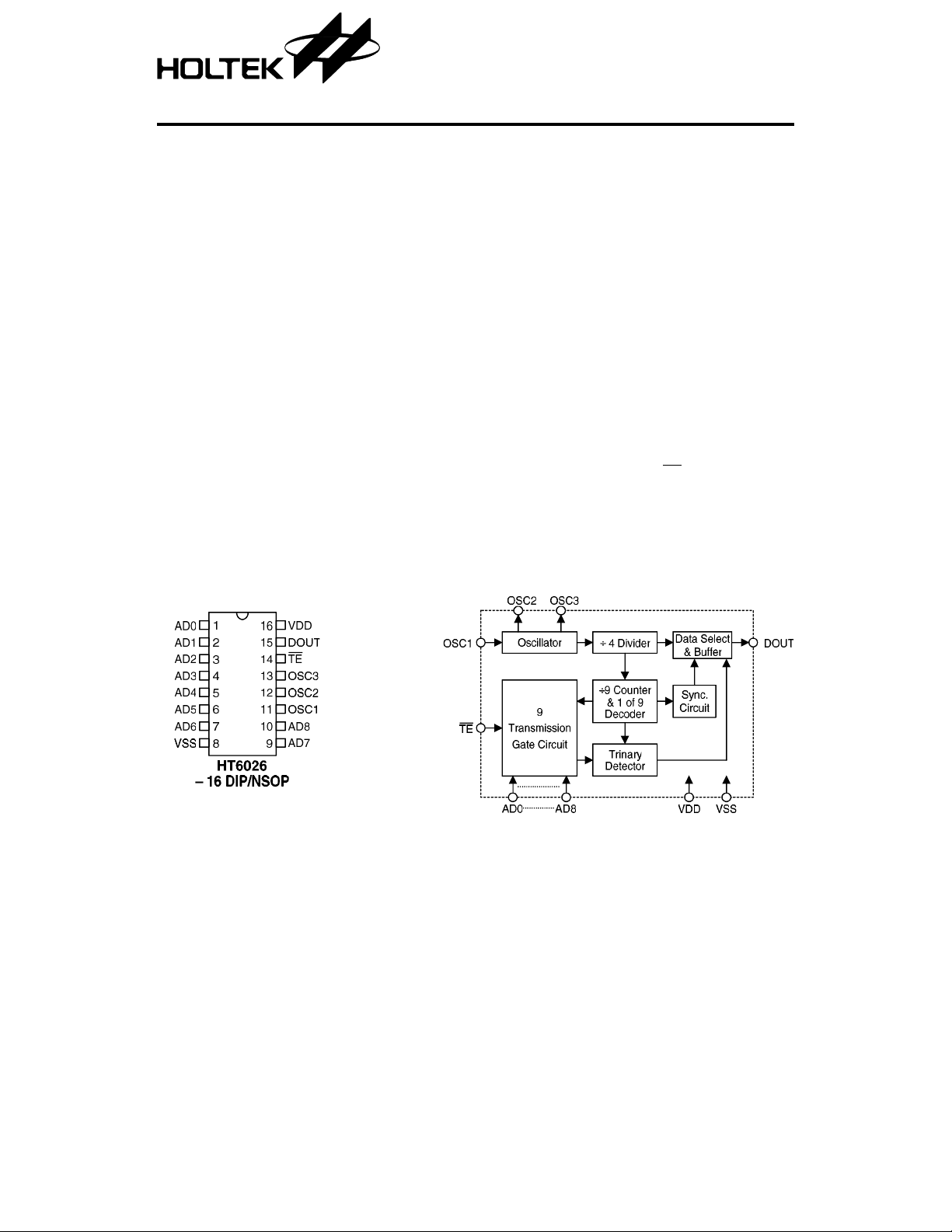
Pin Assignment Block Diagram
1 2nd Oct ’97
Page 2
HT6026
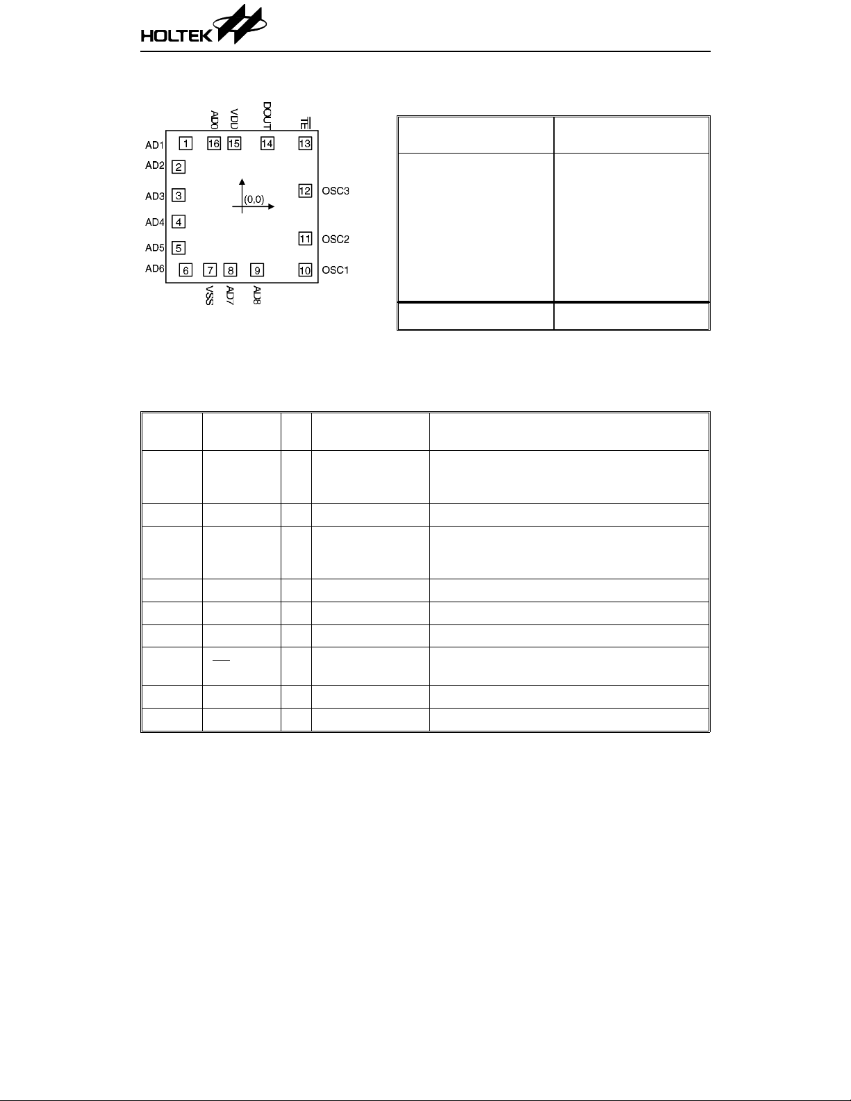
Pad Coo rd i n a te s Unit:
µm
Pad
No.
1 –598.00 689.00 9 160.00 –687.00
2 –674.00 433.00 10 670.00 –687.00
3 –674.00 126.00 11 670.00 –347.00
4 –674.00 –162.00 12 670.00 172.00
5 –674.00 –449.00 13 670.50 689.50
6 –598.00 –687.00 14 270.00 689.00
7 –342.00 –687.00 15 –84.00 689.00
8 –127.00 –687.00 16 –299.00 689.00
Chip size: 1650
* The IC substrate should be connected to VSS in the PCB layout artwork.
× 1680 (µm)
2
XY
Pad
No.
XY
Pin Description
Pin No. Pin Name I/O
1~7 AD0~AD6 I
8 VSS I — Negative power supply (GND)
9~10 AD7~AD8 I
11 OSC1 I OSCILLATOR Oscillator input pin
12 OSC2 O OSCILLATOR Oscillator output pin
13 OSC3 O OSCILLATOR Oscillator output pin
14
15 DOUT O CMOS OUT Encoder data serial transmission output
16 VDD — Positive power supply
TE I
Internal
Connection
TRANSMISSION
GATE
TRANSMISSION
GATE
CMOS IN
Pull-High
Description
Input pins for address/data AD0~AD6 setting
They can be externally set to VDD, VSS, or left
open
Input pins for address/data AD7~AD8 setting
They can be externally set to VDD, VSS, or left
open
Transmission enable, active low
2 2nd Oct ’97
Page 3
HT6026
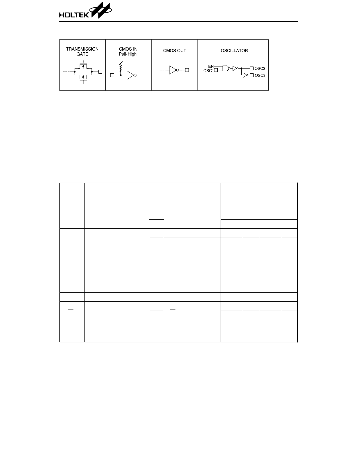
Approximate i nte r na l co nn ec t ion circuits
Absolute Maximum Ratings*
Supply Voltage...............................–0.3V to 24V
Input Voltage....................V
–0.3 to VDD+0.3V
SS
*Note: Stresses above those listed under “Absolute Maximum Ratings” may cause permanent
damage to the device. The se are stress ratings on ly. Functional operatio n of this device at
these or any other conditions above those indicated in the operational sections of this
specification is not implied and exposure to absolute maximum rating conditions for extened
periods may affect device reliability.
Storage Temperature.................–50
Operating Temperature...............–20
°C to 125°C
°C to 75°C
Electrical Characteristics
Symbol Parameter
V
DD
I
STB
I
DD
I
DOUT
V
IH
V
IL
R
TE
F
OSC
Operating Voltage — — 4 — 18 V
Standby Current
Operating Current
Output Drive Current
“H” Input Voltage — — 0.7V
“L” Input Voltage — — 0 — 0.3V
TE Pull-High Res is tance
Oscillator Frequency
(Ta=25°C)
Test Conditions
V
DD
5V
Conditions
Oscillator stops
15V — 0.1 0.5
5V No load, F
15V No load, F
5V
15V –8.0 –14.0 — mA
5V
15V 5.0 10.0 — mA
5V
=0.9VDD (Source)
V
OH
=0.1VDD (Sink)
V
OL
VTE=0V
=18kHz — 500 900
OSC
=22kHz — 2000 3000
OSC
15V — 250 —
=10kΩ
R
EXT
5V
C
=2000PF
R
EXT
S=
20kΩ
15V — 22 — kHz
Min. Typ. Max. Unit
— 0.1 0.3
µA
µA
µA
µA
–1.0 –1.7 — mA
0.8 1.5 — mA
—VDD V
DD
V
DD
—800—
k
k
—18—kHz
Ω
Ω
3 2nd Oct ’97
Page 4

HT6026
Functional Description
Operation
The HT6026 encoder begins a one-word transmission cycle upon rec eipt of a transmission enable ( TE,
active low). This cycle will repeat itself as long as the transmission enable (
transmission enable returns high, the encoder output completes its final N
stops as shown in Figure 1. The total number of transmission cycles allowed is always adjuste d to an
even number automatically.
Figure 1. Transmission timing
Information word
An information word consists of 2 periods as shown:
TE ) is held low. Once the
×2 word cycle, and then
Figure 2. Composition of information
Address/data waveform
Each programmable address/data pin can be externally set to one of the following three logic states:
Figure 3. Address/Data bit waveform
4 2nd Oct ’97
Page 5

HT6026
Address/dat a pr o gr a mmi n g (pr e set)
The status of each address/data pin can be individually pre-set to logic “high”, “low”, or “floating”. If a transmission enable signal is appl ie d,
the encode r scans and transmits the status of
9-bit address/data serially in the order AD0 to
AD8. But if the trigger signal is not applied, the
chip only consumes a sta ndb y current which is
less than 1
The transmitted information is as listed:
Pilot
µA (for VDD=5V).
AD0
AD1
AD2
AD3
&
Sync.
1
Z
1
Z
The address pins are usually pre-set to transmit
data codes with their own particular security
codes by the DIP switches or PCB wiring, while
the data is selected by the push button or electronic switches.
The following figure demo nstrates an application using the HT 6026:
AD4
Z
AD5
Z
AD6
0
AD7
1
AD8
Z
Z: floating
5 2nd Oct ’97
Page 6

HT6026
Transmission enable
Transmission is enabled by applying a low signal to the TE pin. The HT6026 is enab le d and ou t put s
address/data codes from DOUT pin when the
Flowchart
Oscillator fr equency vs supply voltage
TE is set to “low” and more than 65ns.
6 2nd Oct ’97
Page 7

Application Circuit
Note: Typical infrared diode: EL-1L2 (KODENSHI CORP.)
Typical RF transmitter: JR-220 (JUWA CORP.)
HT6026
7 2nd Oct ’97
 Loading...