

1K/2K 2-Wire CMOS Serial EEPROM
Features
•
Operating voltage: 2.4V ~5.5V
•
Low power consumption
–
Operation: 5mA max.
–
Standby: 5µA max.
•
Internal organization
–
1K (HT24LC01):128×8
–
2K (HT24LC02): 256×8
•
2-wire serial interface
•
Write cycle time: 5ms max.
•
Automatic erase-before-write operation
General Description
The HT24LC01/02 is a 1K/2K-bit serial
read/write non-volatile memory device using
the CMOS floating gate process. Its 1024/2048
bits of memory are organized into 128/256
words and each word is 8 bits. The device is
optimized for use in m any industri al and com -
HT24LC01/02
•
Partial page write allowed
•
8-byte Page write modes
•
Write operation with built-in timer
•
Hardware controlled write protection
•
40-year data retention
•
106 erase/write cycles per word
•
8-pin DIP/SOP package
•
8-pin TSSOP (HT24LC02 only)
•
Commerical temperature range
(0
°C to +70°C)
mercial applications where low power and low
voltage operation are essential. Up to eight
HT24LC01/02 de vices may b e conn ected to th e
same two-wire bus. The HT 24LC 01/02 is gua ranteed for 1M erase/write cycles and 40-year
data retention.
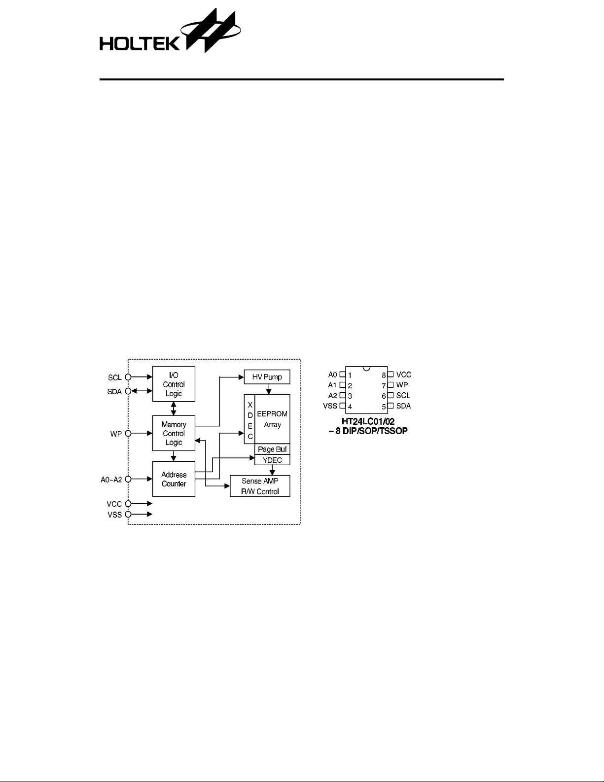
Block Diagram Pin Assignme nt
1 6th May ’99
HT24LC01/02
Pin Description
Pin Name I/O Description
A0~A2 I Address inputs
SDA I/O Serial data inputs/output
SCL I Serial clock data input
WP I Write protect
VSS — Negative power supply
VCC I Positive power supply
Absolu te Maxim um Ratings
Operating Temperature (Commercial) .................................................................................. 0°C to 70°C
Storage T emperature ..................... .... .. .. .... .. .. .... .. .. .... .. .. .... .. .. .... .. .. .... .. .. .... .. .. .... .. .. .... .. .. ... –50
Applied VCC Voltage with Respect to VSS ................ .. ................ .. .. ................ .. .. ............. –0.3V to 6.0V
Applied V oltage on any Pin with Respect to VSS
...................................................................
–0.3V to VCC+0.3V
Note: These are stress ratings only. Stresses exceeding the range specifie d under “Absolute Maxi-
mum Ratings” may cause substantial damage to the device. Functional operation of this device
at other conditions beyond those listed in the specification is not implied and prolonged
exposure to extreme condition s may affect device reliability.
°C to 125°C
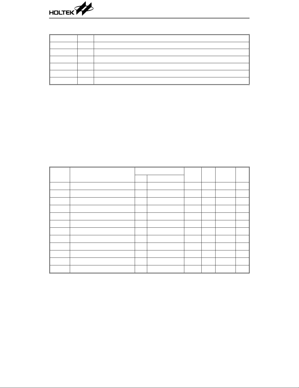
D.C. Characteristics Ta=0°C to 70°C
Symbol Parameter
V
CC
I
CC1
I
CC2
V
IL
V
IH
V
OL
I
LI
I
LO
I
STB1
I
STB2
C
IN
C
OUT
Operating Voltage — — 2.4 — 5.5 V
Operating Current 5V Read at 100kHz — — 2 mA
Operating Current 5V Write at 100kHz — — 5 mA
Input Low Voltage — — –1 — 0.3V
Input High Voltage — — 0.7V
Output Low Voltage 2.4V IOL=2.1mA — — 0.4 V
Input Leakage Current 5V VIN=0 or V
Output Leakage Current 5V V
Standby Current 5V VIN=0 or V
Standby Current 2.4V VIN=0 or V
Input Capacitance (See Note) — f=1MHz 25°C——6pF
Output Capacitance (See Note) — f=1MHz 25°C——8pF
Note: These parameters are periodically sampled but not 100% tested
Test Conditions
V
Conditions
CC
CC
=0 or V
OUT
CC
CC
2 6th May ’99
Min. Typ. Max. Unit
—VCC+0.5 V
CC
—— 1 µA
CC
—— 1 µA
—— 5 µA
—— 4 µA
CC
V
HT24LC01/02
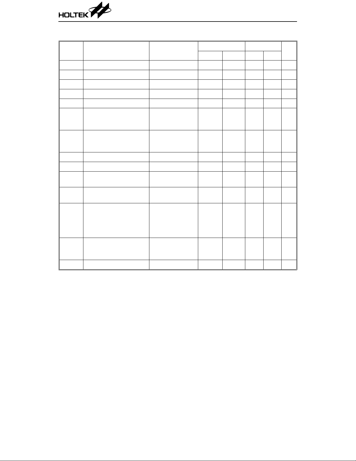
A.C. Characteristics Ta=0°C to 70°C
Symbol Parameter Remark
f
SK
t
HIGH
t
LOW
t
R
t
F
t
HD:STA
t
SU:STA
t
HD:DAT
t
SU:DAT
t
SU:STO
t
AA
Clock Frequency — 100 — 400 kHz
Clock High Time 4000 — 600 — ns
Clock Low Time 4700 — 1200 — ns
SDA and SCL Rise Time Note — 1000 — 300 ns
SDA and SCL Fall Time Note — 300 — 300 ns
START Condition Hold
Time
START Condition
Setup Time
After this period
the first clock pulse
is generated
Only relevant for
repeated START
condition
Data Input Hold Time 0 — 0 — ns
Data Input Setup Time 200 — 1 00 — ns
STOP Condition Setup
Time
Output Valid from
Clock
Time in which the
bus must be free
t
BUF
Bus Free Time
before a new
transmission can
start
t
SP
t
WR
Input Filter Time
Constant (SDA and SCL
Pins)
Write Cycle Time — 5 — 5 ms
Noise suppression
time
Standard Mode* V
=5V±10%
CC
Unit
Min. Max. Min. Max.
4000 — 600 — ns
4000 — 600 — ns
4000 — 600 — ns
— 3500 — 900 ns
4700 — 1200 — ns
—100—50ns
Notes: These parameters are periodically sampled but not 100% tested
* The standard mode means V
=2.4V to 5.5V
CC
For relative timing, refer to timing diagrams
3 6th May ’99

Functional Description
•
Serial clock (SCL)
The SCL input is used for positive edge clock
data into each EE PR OM de vice and ne gati ve
edge clock data out of each device.
•
Serial data (SDA)
The SDA pin is bidirectional for serial data
transfer. The pin is open-drain driven and
may be wired-OR with any number of other
open-drain or open collector devices.
•
A0, A1, A2
The A2, A1 and A0 pins are device address
inputs that are hard wired for the
HT24LC01/02. As many as eight 1K/2K devices may be addressed on a single bus system
(the device addressing is discuss ed in detail
under the Device Addressing section).
•
Write protect (WP)
The HT24LC01/02 has a write protect pin
that provides hard ware data protection. The
write protect pin allows normal read/write
operations whe n connected to the V
the write protect pin is connected to Vcc, the
write protection fe ature is enable d and ope rates as shown in the following table.
WP Pin
Status
At V
CC
At V
SS
HT24LC01 HT24LC02
Full Array (1K) Full Array (2K)
Normal Read/Write Operations
Protect Array
. When
SS
HT24LC01/02
bus is not busy. During data transfer, the data
line must remain stable whenever the clock
line is high. Changes in data line while the
clock line is high will be interpreted as a
START or STOP condition.
•
Start condition
A high-to-low transition of SDA with SCL high
is a start conditi on which must precede a ny
other command (refer to Start and Stop Definition Timing diagram).
•
Stop condition
A low-to-high transition of SDA with SCL high
is a stop condition. After a read sequence, the
stop command will place the EEPROM in a
standby power mode (refer to Start and Stop
Definition Timing Diagram).
•
Acknowledge
All addresses and data words are serially
transmitted to and from the EEPROM in 8-bit
words. The EEPROM sends a zero to acknowledge that it has received each word. This
happens during the ninth clock cycle.
Memory organization
•
HT24LC01, 1K Serial EEPROM
Internally organized with 128 8-bit words, the
1K requires a 7-bit data word address for
random word addressing.
•
HT24LC02, 2K Serial EEPROM
Internally organized with 256 8-bit words, the
2K requires an 8-bit data word address for
random word addressing.
Device operations
•
Clock and data transition
Data transfer may be initiated only when the
Device addressing
The 1K and 2K EEPROM devices all require an
8-bit device address word following a start condition to enable the chip for a read or write
operation. The device address word consist of a
mandatory one, zero sequence for the first four
most significant bits (refer to the diagram showing the Device Addres s). This is common to al l
the EEPROM device.
The next three bits are the A2, A1 and A0 device
address bits for the 1K/2K EEPROM. These
three bits must compare to their corresponding
hard-wired input pins.
4 6th May ’99

HT24LC01/02
The 8th bit of device address is the read/write
operation select bit. A read operation is in itiated if this bit is high a nd a wri te opera tion is
initiated if this bit is low.
If the comparison of the device address succeed the
EEPROM will output a zero at ACK bit. If not, the
chip will return to a standby state.
Write operations
•
Byte write
A write operation requires an 8-bit data word
address following the device address word
and acknowledgment. Upon receipt of this address, the EEPROM will again respond with a
zero and then clock in the first 8-bit data
word. After receiving the 8-bit data word, the
EEPROM will output a zero and the addressing device, such as a microcontroller, must
terminate the write sequence with a stop condition. At this time the EEPROM enters an
internally-timed write cycle to the non-volatile memory. All inputs are disabled during
this write cycle and EEPROM will not respond until the write is completed (refer to
Byte write timing).
•
Page write
The 1K/2K EEPROM is capable of an 8-byte
page write.
A page write is initiated the same as byte
write, but the microcontroller does not send a
stop condition after the first data word is
clocked in. Instead, after the EEPROM acknowledges the receipt of the first data word,
the microcontrol ler can tran smit up to seve n
more data words. The EEPROM will respond
with a zero after each data word received. The
microcontroller must terminate the page
write sequence with a stop condition.
The data word address lower three (1K/2K)
bits are internally incre mented foll owing the
receipt of each data word. The higher data
word address bits are not incremented, retaining the memory page row locati on (refer
to Page write timing).
•
Acknowledge polling
Since the device will no t acknowle dge duri ng
a write cycle, this can be used to determ ine
when the cycle is complete (this feature can be
used to maximize bus throughput). Once the
stop condition for a write co mmand has bee n
issued from the master, the device initiates
the internally timed write cycle. ACK polling
can be initiated immediately. This involves
the master sending a start condition followed
by the control byte for a write command
(R/W=0). If the device is still busy with the
5 6th May ’99

write cycle, then no AC K will be return ed. If
the cycle is completed, then the device will
return the ACK and the master can then proceed with the next read or write command.
•
Write protect
The HT24LC01/02 can be used as a serial
ROM when the WP pin is connected to VCC.
Programming will be inhibited and the entire
memory will be write-protected.
•
Read operations
Read operations are initiated the same way as
write operations with th e exception that the
read/write select bit in the device address
word is set to one. There are three read operations: current a ddress read, rand om address
read and sequential read.
•
Current address read
The internal data word address counter main-
tains the last address accessed during the last
read or write operati on, incremented by one.
This address stays va lid between operations
as long as the chip power is maintained. The
address roll over during read from the last
byte of the last memory page to the first byte
of the first page. The address roll over during
write from the last byte of the current page to
the first byte of the same page. Once the device address with the read/write select bit set
to one is clocked in and acknowl edged by th e
EEPROM, the current address data word is
serially clocked out . The m icrocon trol le r doe s
not respond with an input zero but generates
a following stop condition (refer to Current
read timing).
HT24LC01/02
Acknowledge polling flow
•
Random read
A random read requires a dummy byte write
sequence to load in the data word address
which is then clocked in and acknowledged by
the EEPROM. The microcontroller must then
generate anothe r start condition . The microcontroller now initiates a current address
read by sending a device address with the
read/write select bit high. The EEPROM acknowledges the device address and serially
clocks out the data word. The microcontroller
does not respond wi th a zero but doe s generates a following stop condition (refer to Ran dom read timing).
6 6th May ’99

•
Sequential read
Sequential reads are initiated by either a cur-
rent address read or a random address read.
After the microcontroller receives a data word,
it responds with an acknowledgment. As long as
the EEPROM receives an acknowledgment, it
will continue to increment the data word address and serially clock out sequential data
Timing Diagrams
HT24LC01/02
words. When the memory address limit is
reached, the data word address will roll over
and the sequential read continues. The sequential read operation is terminated when
the microcontroller does not respond with a
zero but generates a following stop condition.
Note: The write cycle time tWR is the time from a valid stop condition of a write sequence to the end
of the valid start condition of sequential command.
7 6th May ’99

HT24LC01/02
Holtek Semiconductor Inc. (Headquarters)
No.3 Creation Rd. II, Science-based Industrial Park, Hsinchu, Taiwan, R.O.C.
Tel: 886-3-563-1999
Fax: 886-3-563-1189
Holtek Semiconductor Inc. (Taipei Office)
5F, No.576, Sec.7 Chung Hsiao E. Rd., Taipei, Taiwan, R.O.C.
Tel: 886-2-2782-9635
Fax: 886-2-2782-9636
Fax: 886-2-2782-7128 (International sales hotline)
Holtek Microelectronics Enterprises Ltd.
RM.711, Tower 2, Cheung Sha Wan Plaza, 833 Cheung Sha Wan Rd., Kowloon, Hong Kong
Tel: 852-2-745-8288
Fax: 852-2-742-8657
Copyright © 1999 by HOLTEK SEMICONDUCTOR INC.
The information appearing in this Data Sheet is believed to be accurate at the time of publication. However, Holtek
assumes no responsibility arising from the use of the specif ications descri bed. The applications mentioned herein are
used solely for the purpose of illustration and Holtek makes no warranty or representation that such applications
will be suitable without further modification, nor recommends the use of its products for appli cation that may present
a risk to human life due to malfunction or otherwise. Holtek reserves the right to alter its products without prior
notification. For the most up-to-date information, please visit our web site at http://www.holtek.com.tw.
8 6th May ’99
 Loading...