


Features
Operating voltage: 2.7V~5.5V
·
Low power consumption
·
–
Operation: 25mA max. (VCC=5V)
–
Standby: 30mA max. (VCC=5V)
Access time: 120ns max. (VCC=5V)
·
10mA max. (V
10mA max. (V
250ns max. (V
CC
CC
=3V)
CC
=3V)
=3V)
General Description
The HT23C040 is a read-only memory with
high performance CMOS storage device whose
4096K of memory is arranged into 524288 word
by 8 bits.
For application flexibility, the chip enable and
output enable control pins can be selected as ac
tive high or active low. This flexibility not only
allows easy interface with most microproces
sors, but also eliminates bus contention in mul
HT23C040
CMOS 512K´8-Bit Mask ROM
524288´8-bit of mask ROM
·
Mask option: chip enable CE/CE/OE1/OE1,
·
and output enable OE/OE
TTL compatible inputs and outputs
·
Tristate outputs
·
Fully static operation
·
Package type: 32-pin DIP/SOP
·
tiple bus microprocessor systems. An
additional feature of the HT23C040 is its abil
ity to enter the standby mode whenever the
chip enable (CE/CE
current consumption to below 30mA. The combi
nation of these functions makes the chip suit
able for high density low power memory
applications.
-
-
) is inactive, thus reducing
/NC
-
-
-
1 January 20, 2000
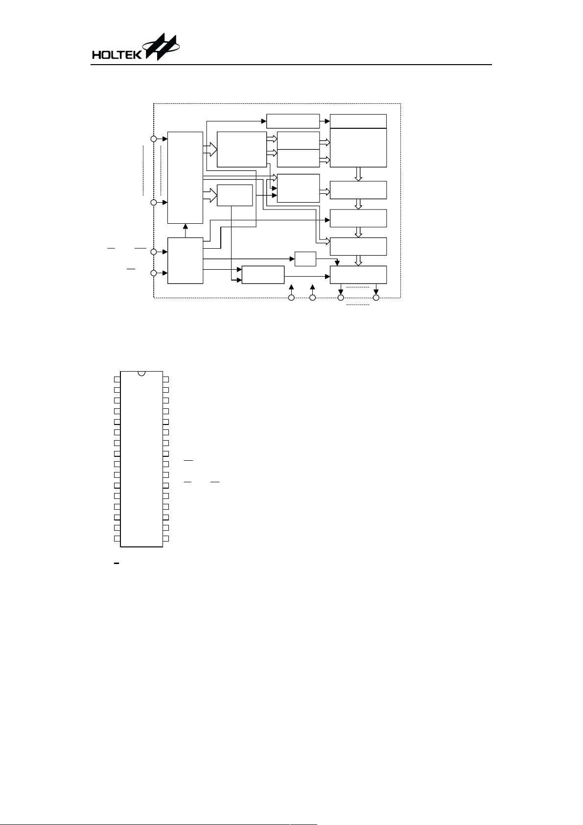
Block Diagram
HT23C040
A0
A18
CE/CE/OE1/O E1
OE/OE/NC
Pin Assignment
1
NC
A16
A15
A12
A7
A6
A5
A4
A3
A2
A1
A0
D0
D1
D2
VSS
32 D IP /S O P
2
3
4
5
6
7
8
9
10
11
12
13
14
15
16
HT23C040
32
31
30
29
28
27
26
25
24
23
22
21
20
19
18
17
Address
Buffers
CTRL
VCC
A18
A17
A14
A13
A8
A9
A11
OE/OE/NC
A10
CE/CE/OE1/O E1
D7
D6
D5
D4
D3
XY
Pre-decoder
ATD
Pre-charge C K T
Latch
X-Dec
Y-Dec
Z-D ec
VSS
Mux
VCC
Pull-high NM O S
ROM Cell
A rra y
(512K
8-Bits)
´
Z-se le ctor
S e n s e A m p lifie rs
Mux
Output Buffers
D0
D7
2 January 20, 2000
Pin Description
Pin Name I/O Description
NC
A0~A18 I Address inputs
D0~D7 O Data outputs
VSS
/OE1/OE1 I Chip enable/Output enable input
CE/CE
/NC I Output enable input
OE/OE
VCC
No connection
¾
Negative power supply
¾
Positive power supply
¾
Operation Truth Table
Mode CE/CE OE/OE A0~A18 D0~D7
Read H/L H/L Valid Data Out
Deselect H/L L/H X High Z
Standby L/H X X High Z
HT23C040
Note: H=VIH, L=VIL, X=VIHor V
IL
Absolute Maximum Ratings
Supply Voltage.................................-0.3V to 6V
Input Voltage .......................-0.3V to V
Note: These are stress ratings only. Stresses exceeding the range specified under ²Absolute Maxi-
mum Ratings² may cause substantial damage to the device. Functional operation of this device
at other conditions beyond those listed in the specification is not implied and prolonged exposure to extreme conditions may affect device reliability.
CC
+0.3V
Storage Temperature.................-50°Cto125°C
Operating Temperature ..............-40°Cto85°C
3 January 20, 2000

D.C. Characteristics
HT23C040
Supply voltage: 4.5V~5.5V
Symbol Parameter
V
CC
I
CC1
V
IL1
V
IH1
V
OL1
V
OH1
I
LI
I
LO
I
STB1
I
STB2
C
IN
C
OUT
Operating Voltage
Operating Current 5V
Input Low Voltage 5V
Input High Voltage 5V
Output Low Voltage 5V
Output High Voltage 5V
Input Leakage Current 5V
Output Leakage Current 5V
Standby Current 5V
Standby Current 5V
Input Capacitance (See note)
Output Capacitance (See note)
Test Conditions
CC
Conditions
V
¾¾
O/P Unload,
f=5MHz
¾
¾
I
=3.2mA
OL
=-1mA
I
OH
V
=0 to V
IN
V
OUT
CE=V
CE=V
=0 to V
IL
IH
CC
CC
CE£0.2V
³VCC-0.2V
CE
f=1MHz
¾
f=1MHz
¾
T
=-40°Cto85°C
a
Min. Typ. Max. Unit
4.5
¾¾
V
SS
2.2
¾¾
2.4
¾¾
¾¾
¾¾
¾¾
¾¾
¾¾
¾
¾
¾
¾
5.5 V
25 mA
0.8 V
V
CC
0.4 V
V
CC
10
mA
10
mA
1.5 mA
30
mA
10 pF
10 pF
V
V
4 January 20, 2000

HT23C040
Supply voltage: 2.7V~3.3V
Test Conditions
Symbol Parameter
CC
Conditions
O/P Unload,
f=5MHz
¾
¾
I
=2mA
OL
=-0.6mA
I
OH
=0 to V
V
IN
V
=0 to V
OUT
f=1MHz
f=1MHz
CC
CC
V
I
V
V
V
V
I
I
C
C
CC
CC2
IL2
IH2
OL2
OH2
LI
LO
IN
OUT
V
Operating Voltage
¾¾
Operating Current 3V
Input Low Voltage 3V
Input High Voltage 3V
Output Low Voltage 3V
Output High Voltage 3V
Input Leakage Current 3V
Output Leakage Current 3V
Input Capacitance (See Note)
Output Capacitance (See Note)
¾
¾
Note: These parameters are periodically sampled but not 100% tested.
A.C. Characteristics
Symbol Parameter
t
CYC
t
AA
t
ACE
t
AOE
t
OH
t
OD
t
OE
Cycle Time 200
Address Access Time
Chip Enable Access Time
Output Enable Access Time
Output Hold Time
Output Disable Time (See Note)
Output Enable Time (See Note)
3V±10% 5V±10%
Min. Max. Min. Max.
¾
¾
¾
¾
250
250
150
¾¾
¾¾¾
¾¾
T
=-40°Cto85°C
a
Min. Typ. Max. Unit
2.7
¾¾
V
SS
1.5
¾¾
1.5
¾¾
¾¾
¾¾
¾¾
¾
¾
¾
¾
3.3 V
10 mA
0.4 V
V
CC
0.4 V
V
CC
10
10
10 pF
10 pF
V
V
mA
mA
Ta=-40°Cto85°C
Unit
120
¾
¾
¾
10
¾
120 ns
120 ns
80 ns
¾
ns
ns
70 ns
10
¾
ns
Note: These parameters are periodically sampled but not 100% tested.
5 January 20, 2000

A.C. test condition
Output load: see figure right
Input rise and fall time: 10ns
Input pulse levels: 0.4V to 2.4V
Input and output timing reference levels:
0.8V and 2.0V (V
1.5V (V
CC
=3V)
CC
=5V)
Functional Description
The HT23C040 has two modes, namely data
read mode and standby mode, controlled by
CE/CE
/OE1/OE1 and OE/OE/NC inputs.
·
Standby mode
The HT23C040 has lower current consumption,
controlled by the chip enable input (CE/CE
When a low/high level is applied to the CE/CE
input regardless of the output enable
(OE/OE
standby mode.
/NC) states, the chip will enter the
HT23C040
V
CC
1250
W
Output
775
W
* Including scope and jig
Output load circuit
·
Data read mode
When both the chip enable (CE/CE/
and the output enable (OE/OE
the chip is in data read mode. Otherwise, ac
tive CE/CE
).
deselect mode. The output will remain in Hi-Z
state.
and inactive OE/OE/NC result in
100pF*
OE1/OE1)
/NC) are active,
-
Timing Diagrams
·
Propagation delay due to address (CE/CE/OE1/OE1 and OE/OE are active)
t
CYC
t
t
ACE
AA
t
Valid
AOE
t
OH
Valid
t
OD
Valid
6 January 20, 2000
Address
D out
·
Propagation delay due to chip and output enable (address valid)
CE
CE
OE
OE
t
OE
D out

Characteristic Curves
HT23C040
CC
(N o rm a lize d )
O perating C urrent I
Ta=25 C
STB2
(N o rm a lize d )
Standby Current I
Ta=25 C
1.5
1.25
1
0.75
0.5
4.5 5 5.5
O perating V oltage VCC (V)
1.5
1.25
1
0.75
0.5
4.5 5 5.5
O perating V oltage V
CC
(V )
1.2
CC
1.1
1
0.9
(N o rm a lize d )
O perating C urrent I
0.8
-5 0 -2 5 0 2 5 5 0 7 5
V
CC
=5V
Tem perature ( C )
1.4
STB2
1.25
1.1
(N o rm a lize d )
0.95
Standby Current I
0.8
-5 0 -2 5 0 2 5 5 0 7 5
V
CC
=5V
Tem perature ( C )
AA
(N o rm a lize d )
A ccess Tim e T
Ta=25 C
1.2
1.1
1
0.9
0.8
4.5 5 5.5
O perating V oltage V
CC
( V )
1.5
1.25
AA
1
(N o rm a lize d )
0.75
A ccess Tim e T
0.5
-5 0 -2 5 0 2 5 5 0 7 5
V
CC
=5V
Tem perature ( C )
7 January 20, 2000

HT23C040
ACE
(N o r m a liz e d )
A ccess Tim e T
Ta=25 C
AOE
(N o r m a liz e d )
A ccess Tim e T
Ta=25 C
1.2
1.1
1
0.9
0.8
4.5 5 5.5
O perating Voltage V
CC
( V )
1.2
1.1
1
0.9
0.8
4.5 5 5.5
O perating Voltage VCC ( V )
ACE
A ccess Tim e T
VCC=5V
AOE
(N o rm a lize d )
A ccess Tim e T
VCC=5V
1.5
1.25
1
(N o r m a liz e d )
0.75
0.5
-5 0 -2 5 0 2 5 5 0 7 5
Tem perature ( C )
1.5
1.25
1
0.75
0.5
-5 0 -2 5 0 2 5 5 0 7 5
Tem perature ( C )
100
8 January 20, 2000

HT23C040 MASK ROM ORDERING SHEET
Custom:
Input Medium:
EPROM DISK File (Mail Address: romfile@holtek.com.tw) OTHER
HT23C040
User No. Type/Ref. Name
Control Pin and Package Form Option:
(a) 32 Pin Type Pin 22:
Pin 24: (1) OE (2) OE (3) NC
(b) Package Form:
Companion User No.
Package Marking :
Delivery Date : Q¢ty:
CUSTOM CONFIRMED BY:
(1) Chip Form (2) 32 DIP (3) 32 SOP
(1) CE (2) CE (3) OE1 (4) OE1
Q¢ty
Check Sum
Memory Address
Start End
(NAME, DATE, POSITION & CO. CHOP)
HOLTEK CONFIRMED BY:
(SALES) (SALES MANAGER)
9 January 20, 2000

HT23C040
Holtek Semiconductor Inc. (Headquarters)
No.3 Creation Rd. II, Science-based Industrial Park, Hsinchu, Taiwan, R.O.C.
Tel: 886-3-563-1999
Fax: 886-3-563-1189
Holtek Semiconductor Inc. (Taipei Office)
5F, No.576, Sec.7 Chung Hsiao E. Rd., Taipei, Taiwan, R.O.C.
Tel: 886-2-2782-9635
Fax: 886-2-2782-9636
Fax: 886-2-2782-7128 (International sales hotline)
Holtek Semiconductor (Hong Kong) Ltd.
RM.711, Tower 2, Cheung Sha Wan Plaza, 833 Cheung Sha Wan Rd., Kowloon, Hong Kong
Tel: 852-2-745-8288
Fax: 852-2-742-8657
Copyright ã 2000 by HOLTEK SEMICONDUCTOR INC.
The information appearing in this Data Sheet is believed to be accurate at the time of publication. However, Holtek
assumes no responsibility arising from the use of the specifications described. The applications mentioned herein are
used solely for the purpose of illustration and Holtek makes no warranty or representation that such applications
will be suitable without further modification, nor recommends the use of its products for application that may pres
ent a risk to human life due to malfunction or otherwise. Holtek reserves the right to alter its products without prior
notification. For the most up-to-date information, please visit our web site at http://www.holtek.com.tw.
10 January 20, 2000
-
 Loading...