


96´32 LCD Controller for I/O MCU
Technical Document
·
FAQs
·
Application Note
Features
·
Operating voltage: 2.7V~5.2V
·
Built-in 32kHz RC oscillator
·
External 32.768kHz crystal oscillator or 32kHz fre
quency source input
·
Standby current: <1mA at 3V, <2mAat5V
·
Internal resistor type: 1/6 bias or 1/5 bias, 1/32 duty,
or 1/16 duty
·
Three selectable LCD frame frequencies: 64Hz,
89Hz or 170Hz
·
Max. 96´32 patterns, 96 segments and 32 commons
·
112 segments and 16 commons selectable by com
mand method
·
Built-in bit-map display RAM: 3072 bits(=96´32bits)
·
Built-in internal resistor type bias generator
HT1660
·
Six-wire interface (four data wires)
·
Eight kinds of time base/WDT selection
·
-
-
Time base or WDT overflow output
·
R/W address auto increment
·
Built-in buzzer driver (2kHz/4kHz)
·
Power down command reduces power consumption
·
Software configuration feature
·
Data mode and Command mode instructions
·
Three data accessing modes
·
Provides VLCD pin to adjust LCD operating voltage
and max. VLCD voltage up to 7V
·
Provides three kinds of bias current programming
·
Control of TN-type and STN-type LCDs
·
208-pin QFP package
Applications
·
Leisure products
·
Games
·
Personal digital assistant
General Description
HT1660 is a peripheral device specially designed for I/O
type
max. display segment of the device are 3072 patterns
(96 segments and 32 commons). It also supports four
data bits interface, buzzer sound, Watchdog Timer or
time base timer functions. The HT1660 is a memory
mapping and multi-function LCD controller. Since the
used to expand the display capability. The
MCU
·
Cellular phone
·
Global positioning system
·
Consumer electronics
HT1660 can control TN-type (Twisted Nematic) or
STN-type (Super Twisted Nematic) LCDs. The software
configuration feature of the HT1660 make it suitable for
multiple LCD applications including LCD modules and
display subsystems. Only six lines (CS
,WR, DB0~DB3)
are required for the interface between the host controller
and the HT1660.
Rev. 1.30 1 April 13, 2006
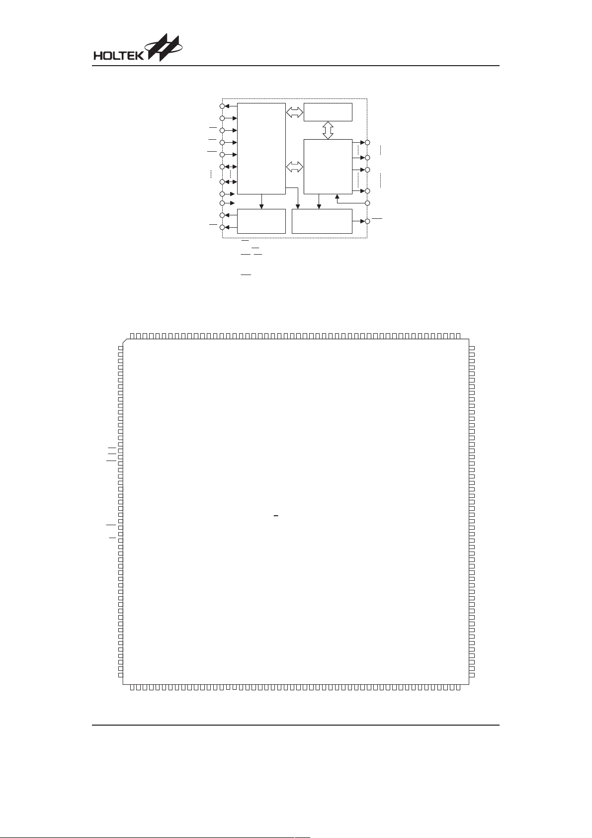
Block Diagram
O S C O
O S C I
C S
R D
W R
D B 0
D B 3
V D D
V S S
B Z
B Z
N o t e : C S : C h i p s e l e c t i o n
D i s p l a y R A M
C o n t r o l
&
T i m i n g
C i r c u i t
T o n e F r e q u e n c y
G e n e r a t o r
B Z , B Z : T o n e o u t p u t s
W R , R D : W R I T E c l o c k , R E A D c l o c k
D B 0 ~ D B 3 : D a t a b u s
C O M 0 ~ C O M 3 1 , S E G 0 ~ S E G 9 5 : L C D o u t p u t s
I R Q : T i m e b a s e o r W D T o v e r f l o w o u t p u t
L C D D r i v e r /
B i a s C i r c u i t
W a t c h d o g T i m e r
&
T i m e B a s e G e n e r a t o r
HT1660
C O M 0
C O M 3 1
S E G 0
S E G 9 5
V L C D
I R Q
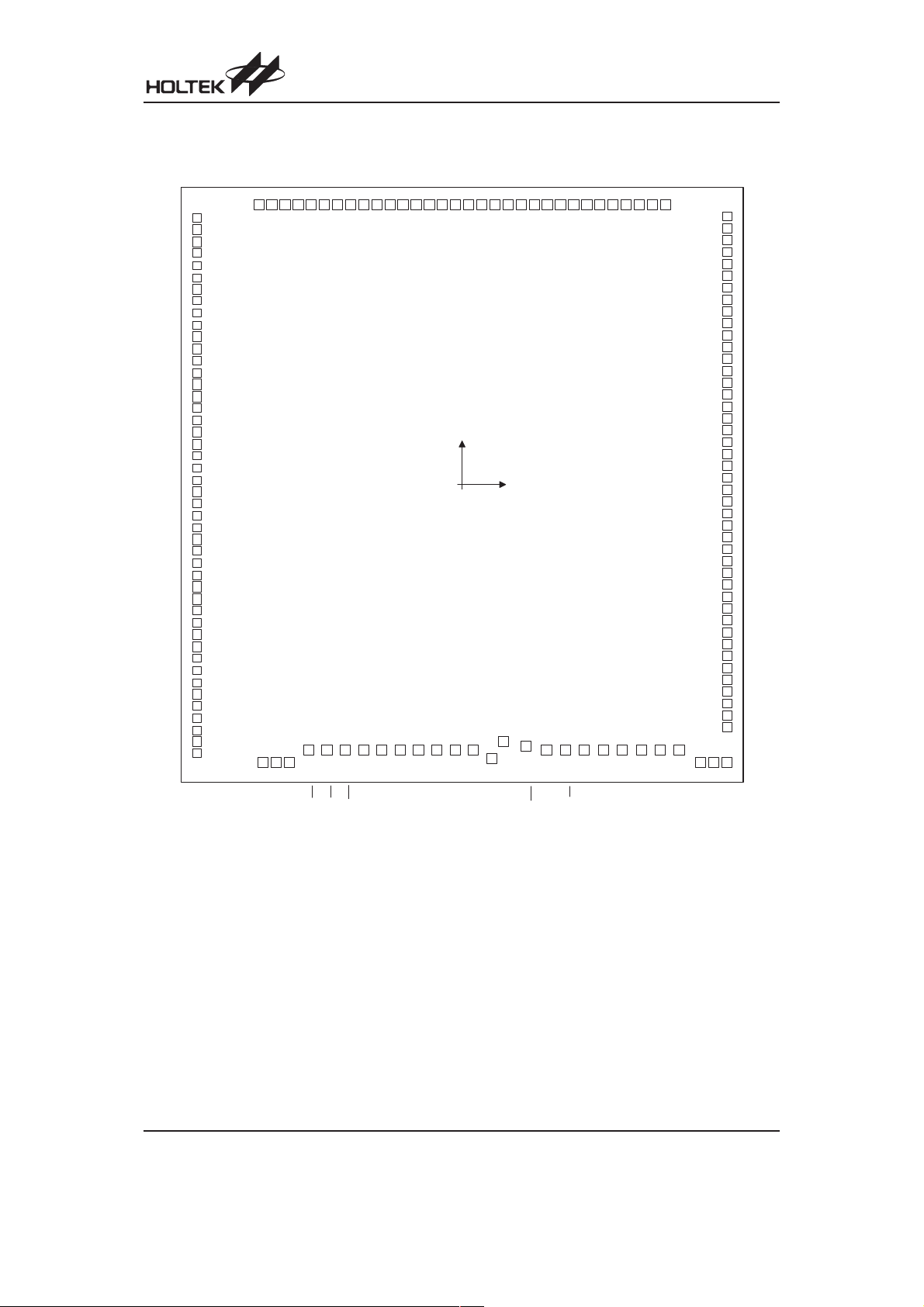
Pin Assignment
C O M 2 2
C O M 2 1
C O M 2 0
C O M 1 9
C O M 1 8
C O M 1 7
C O M 1 6
O S C O
C O M 0
C O M 1
C O M 2
C O M 3
C O M 4
C O M 5
C O M 6
O S C I
V D D
V L C D
T 0 0 0
V L C D
D B 0
D B 1
D B 2
D B 3
V S S
C O M 2 3
C O M 2 4
C O M 2 5
C O M 2 6
C O M 2 7
2 0 8
2 0 7 2 0 6 2 0 5 2 0 4 2 0 3 2 0 2 2 0 1 2 0 0 1 9 9 1 9 8 1 9 7 1 9 6 1 9 5 1 9 4 1 9 3 1 9 2 1 9 1 1 9 0 1 8 9 1 8 8 1 8 7 1 8 6 1 8 5 1 8 4 1 8 3 1 8 2 1 8 1 1 8 0 1 7 9 1 7 8 1 7 7 1 7 6 1 7 5 1 7 4 1 7 3 1 7 2 1 7 1 1 7 0 1 6 9 1 6 8 1 6 7 1 6 6 1 6 5 1 6 4 1 6 3 1 6 2 1 6 1 1 6 0 1 5 9 1 5 8 1 5 7
1
2
3
4
5
6
7
8
N C
9
N C
1 0
N C
1 1
N C
1 2
N C
1 3
N C
1 4
N C
1 5
N C
1 6
N C
1 7
C S
1 8
R D
1 9
W R
2 0
2 1
2 2
2 3
2 4
2 5
2 6
2 7
2 8
2 9
I R Q
3 0
B Z
3 1
B Z
3 2
T 1
3 3
T 2
3 4
T 3
3 5
T 4
3 6
3 7
3 8
N C
3 9
N C
4 0
N C
4 1
N C
4 2
N C
4 3
N C
4 4
N C
4 5
N C
4 6
4 7
4 8
4 9
5 0
5 1
5 2
5 3
5 4 5 5 5 6 5 7 5 8 5 9 6 0 6 1 6 2 6 3 6 4 6 5 6 6 6 7 6 8 6 9 7 0 7 1 7 2 7 3 7 4 7 5 7 6 7 7 7 8 7 9 8 0 8 1 8 2 8 3 8 4 8 5 8 6 8 7 8 8 8 9 9 0 9 1 9 2 9 3 9 4 9 5 9 6 9 7 9 8 9 9
C O M 7
C O M 8
C O M 9
C O M 1 0
C O M 1 1
C O M 2 8
C O M 2 9
C O M 3 0
C O M 3 1
N C
N C
N C
N C
N C
N C
N C
N C
N C
N C
N C
N C
N C
S E G 9 4
S E G 9 5
N C
N C
N C
S E G 8 9
S E G 9 0
S E G 9 1
S E G 9 2
S E G 9 3
S E G 8 4
S E G 8 5
S E G 8 6
S E G 8 7
S E G 8 8
S E G 7 9
S E G 8 0
S E G 8 1
S E G 8 2
S E G 8 3
S E G 7 4
S E G 7 5
S E G 7 6
S E G 7 7
S E G 7 8
H T 1 6 6 0
2 0 8 Q F P - A
S E G 2 1
S E G 2 0
S E G 1 9
S E G 1 8
S E G 1 7
S E G 1 6
S E G 1 5
S E G 1 4
S E G 1 3
S E G 1 2
S E G 1 1
S E G 1 0
S E G 9
S E G 8
S E G 7
S E G 6
S E G 5
S E G 4
S E G 3
S E G 2
S E G 1
S E G 0
N C
N C
N C
N C
N C
N C
N C
N C
N C
N C
N C
N C
N C
N C
N C
N C
C O M 1 2
C O M 1 3
C O M 1 4
C O M 1 5
S E G 7 1
S E G 7 2
S E G 7 3
1 0 0 1 0 1 1 0 2 1 0 3 1 0 4
S E G 2 5
S E G 2 4
S E G 2 3
S E G 2 2
S E G 6 9
S E G 7 0
1 5 6
S E G 6 8
1 5 5
S E G 6 7
1 5 4
S E G 6 6
1 5 3
S E G 6 5
1 5 2
S E G 6 4
1 5 1
S E G 6 3
1 5 0
S E G 6 2
1 4 9
S E G 6 1
1 4 8
S E G 6 0
1 4 7
S E G 5 9
1 4 6
S E G 5 8
1 4 5
S E G 5 7
1 4 4
S E G 5 6
1 4 3
S E G 5 5
1 4 2
S E G 5 4
1 4 1
S E G 5 3
1 4 0
S E G 5 2
1 3 9
S E G 5 1
1 3 8
S E G 5 0
1 3 7
S E G 4 9
1 3 6
S E G 4 8
1 3 5
N C
1 3 4
N C
1 3 3
N C
1 3 2
N C
1 3 1
N C
1 3 0
N C
1 2 9
N C
1 2 8
N C
1 2 7
N C
1 2 6
N C
1 2 5
S E G 4 7
1 2 4
S E G 4 6
1 2 3
S E G 4 5
1 2 2
S E G 4 4
1 2 1
S E G 4 3
S E G 4 2
1 2 0
S E G 4 1
1 1 9
S E G 4 0
1 1 8
S E G 3 9
1 1 7
S E G 3 8
1 1 6
S E G 3 7
1 1 5
S E G 3 6
1 1 4
S E G 3 5
1 1 3
1 1 2
S E G 3 4
1 1 1
S E G 3 3
1 1 0
S E G 3 2
1 0 9
S E G 3 1
1 0 8
S E G 3 0
1 0 7
S E G 2 9
1 0 6
S E G 2 8
1 0 5
S E G 2 7
S E G 2 6
Rev. 1.30 2 April 13, 2006
HT1660
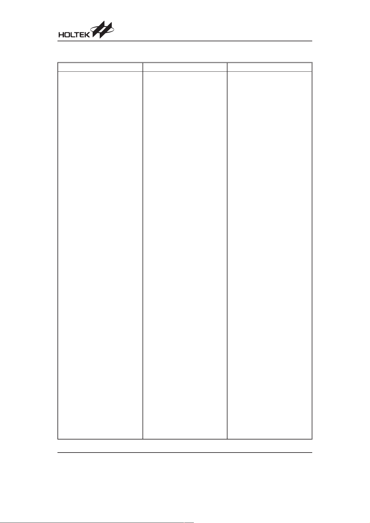
Pad Assignment
1
S E G 6 3
2
S E G 6 4
3
S E G 6 5
4
S E G 6 6
5
S E G 6 7
6
S E G 6 8
7
S E G 6 9
8
S E G 7 0
9
S E G 7 1
1 0
S E G 7 2
1 1
S E G 7 3
1 2
S E G 7 4
1 3
S E G 7 5
S E G 7 6
1 4
S E G 7 7
1 5
S E G 7 8
1 6
S E G 7 9
1 7
S E G 8 0
1 8
S E G 8 1
1 9
S E G 8 2
2 0
S E G 8 3
2 1
S E G 8 4
2 2
S E G 8 5
2 3
2 4
S E G 8 6
2 5
S E G 8 7
2 6
S E G 8 8
2 7
S E G 8 9
2 8
S E G 9 0
2 9
S E G 9 1
3 0
S E G 9 2
3 1
S E G 9 3
3 2
S E G 9 4
3 3
S E G 9 5
3 4
C O M 3 1
3 5
C O M 3 0
3 6
C O M 2 9
3 7
C O M 2 8
3 8
C O M 2 7
C O M 2 6
3 9
C O M 2 5
4 0
C O M 2 4
4 1
C O M 2 3
4 2
C O M 2 2
4 3
C O M 2 1
4 4
C O M 2 0
4 5
C O M 1 9
4 6
S E G 3 1
S E G 3 2
S E G 3 3
S E G 3 4
S E G 3 5
S E G 3 6
S E G 3 7
S E G 3 8
S E G 3 9
S E G 4 0
S E G 4 1
S E G 4 2
S E G 4 3
S E G 4 4
S E G 4 5
S E G 4 6
S E G 4 7
S E G 4 8
S E G 4 9
S E G 5 0
S E G 5 1
S E G 5 2
S E G 5 3
S E G 5 4
S E G 5 5
S E G 5 6
S E G 5 7
S E G 5 8
S E G 5 9
S E G 6 0
S E G 6 1
S E G 6 2
1 4 1
1 4 8
1 4 7
1 4 6
1 4 9
4 7
4 8
4 9
C O M 1 7
C O M 1 8
1 4 3
5 0
5 1
R D
C S
C O M 1 6
1 3 9
1 4 0
5 2
5 3
5 4
W R
D B 0
D B 1
1 4 4
1 4 2
1 4 5
1 3 5
1 3 8
1 3 6
1 3 7
5 6
5 5
D B 2
D B 3
1 3 2
1 3 3
1 3 4
( 0 , 0 )
5 9
5 7
5 8
O S C I
V S S
1 2 9
1 2 8
1 3 1
1 3 0
1 2 7
6 1
6 2
6 0
O S C O
V D D
6 3
B Z
I R Q
V L C D
1 2 3
1 2 5
1 2 6
1 2 4
6 4
6 6
6 5
T 2
T 1
B Z
1 1 9
1 2 2
1 1 8
1 2 0
1 2 1
6 8
6 9
6 7
T 3
7 0
T 4
T 0 0 0
1 1 7
S E G 3 0
1 1 6
S E G 2 9
1 1 5
S E G 2 8
1 1 4
S E G 2 7
S E G 2 6
1 1 3
S E G 2 5
1 1 2
S E G 2 4
1 1 1
1 1 0
S E G 2 3
1 0 9
S E G 2 2
1 0 8
S E G 2 1
1 0 7
S E G 2 0
1 0 6
S E G 1 9
1 0 5
S E G 1 8
1 0 4
S E G 1 7
1 0 3
S E G 1 6
1 0 2
S E G 1 5
1 0 1
S E G 1 4
1 0 0
S E G 1 3
S E G 1 2
9 9
S E G 1 1
9 8
S E G 1 0
9 7
S E G 9
9 6
S E G 8
9 5
S E G 7
9 4
S E G 6
9 3
S E G 5
9 2
S E G 4
9 1
S E G 3
9 0
S E G 2
8 9
S E G 1
8 8
S E G 0
8 7
C O M 1 5
8 6
C O M 1 4
8 5
C O M 1 3
8 4
C O M 1 2
8 3
C O M 1 1
8 2
C O M 1 0
8 1
C O M 9
8 0
C O M 8
7 9
C O M 7
7 8
C O M 6
7 7
C O M 5
7 6
C O M 4
7 5
C O M 3
7 4
7 2 7 3
7 1
C O M 2
C O M 1
C O M 0
V L C D
Chip size: 4340´5030 (mm)
2
* The IC substrate should be connected to VSS in the PCB layout artwork.
Rev. 1.30 3 April 13, 2006
HT1660
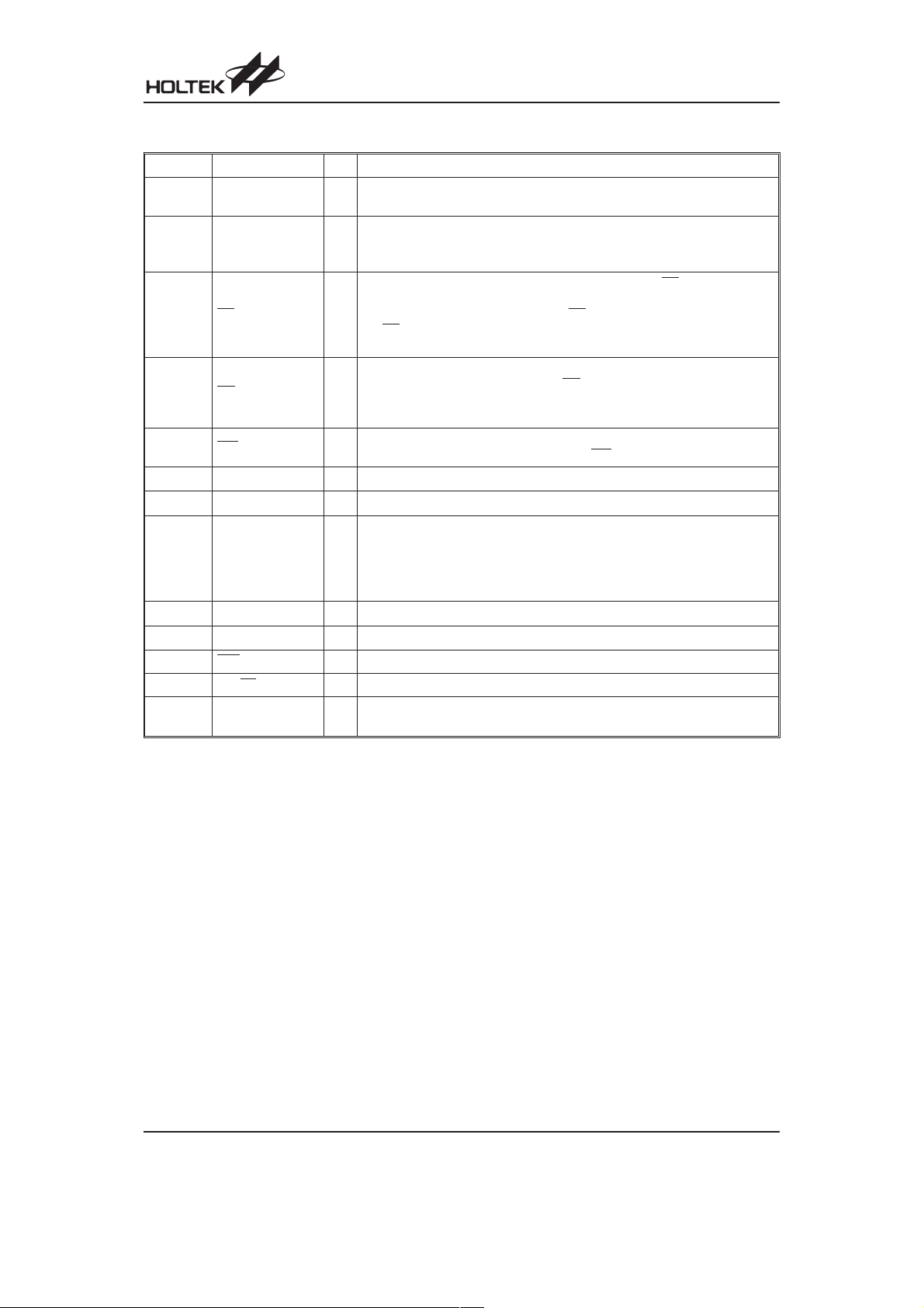
Pad Coordinates
Pad No. X Y Pad No. X Y Pad No. X Y
10
11
12
13
14
15
16
17
18
19
20
21
22
23
24
25
26
27
28
29
30
31
32
33
34
35
36
37
38
39
40
41
42
43
44
45
46
47
48
49
50
1
2
3
4
5
6
7
8
9
-2028.50
-2028.50
-2028.50
-2028.50
-2028.50
-2028.50
-2028.50
-2028.50
-2028.50
-2028.50
-2028.50
-2028.50
-2028.50
-2028.50
-2028.50
-2028.50
-2028.50
-2028.50
-2028.50
-2028.50
-2028.50
-2028.50
-2028.50
-2028.50 -62.80
-2028.50 -162.80
-2028.50 -262.80
-2028.50 -362.80
-2028.50 -462.80
-2028.50 -562.80
-2028.50 -662.80
-2028.50 -762.80
-2028.50 -862.80
-2028.50 -962.80
-2028.50 -1062.80
-2028.50 -1162.80
-2028.50 -1262.80
-2028.50 -1362.80
-2028.50V -1462.80
-2028.50 -1562.80
-2028.50 -1662.80
-2028.50 -1762.80
-2028.50 -1862.80
-2028.50 -1962.80
-2028.50 -2062.80
-2028.50 -2162.80
-2028.50 -2262.80
-1523.55 -2337.10
-1423.55 -2337.10
-1323.55 -2337.10
-1170.45 -2225.20
2237.20 51
2137.20 52
2037.20 53
1937.20 54
1837.20 55
1637.20 56
1537.20 57
1437.20 58
1337.20 59 84.55
1237.20 60 222.85
1237.20 61 310.40
1137.20 62 492.00
1037.20 63 638.50
937.20 64 773.90
837.20 65 933.50
737.20 66 1081.70
637.20 67 1228.70
537.20 68 1376.90
437.20 69 1523.90
337.20 70 1662.50
237.20 71 1821.19
137.20 72 1921.19
37.20 73 2021.19
74 2028.45
75 2028.45
76 2028.45
77 2028.45
78 2028.45
79 2028.45
80 2028.45
81 2028.45
82 2028.45
83 2028.45
84 2028.45
85 2028.45
86 2028.45
87 2028.45
88 2028.45
89 2028.45
90 2028.45
91 2028.45
92 2028.45
93 2028.45
94 2028.45
95 2028.45 54.20 145
96 2028.45 154.20 146
97 2028.45 254.20 147
98 2028.45 354.20 148
99 2028.45 454.20 149
100 2028.45 554.20
-1027.85 -2225.20
-892.45 -2225.20
-745.55 -2225.20
-610.15 -2225.20
-464.85 -2225.20
-329.25 -2225.20
-187.15 -2225.30
-53.65 -2229.70
-2229.70
-2297.35
-2162.35
-2183.60
-2225.30
-2225.30
-2225.30
-2225.30
-2225.30
-2225.30
-2225.30
-2225.30
-2338.90
-2338.90
-2338.90
-2051.10
-1951.10
-1851.10
-1751.10
-1651.10
-1551.10
-1451.10
-1351.10
-1251.10
-1151.10
-1051.10
-951.10
-851.10
-745.80
-645.80
-545.80
-445.80
-345.80
-245.80
-145.80
-45.80
101 2028.45 654.20
102 2028.45 754.20
103 2028.45 854.20
104 2028.45 954.20
105 2028.45 1054.20
106 2028.45 1154.20
107 2028.45 1254.20
108 2028.45 1354.20
109 2028.45 1454.20
110 2028.45 1554.20
111 2028.45 1654.20
112 2028.45 1754.20
113 2028.45 1854.20
114 2028.45 1954.20
115 2028.45 2054.20
116 2028.45 2154.20
117 2028.45 2254.20
118 1550.75 2349.60
119 1450.75 2349.60
120 1350.75 2349.60
121 1250.75 2349.60
122 1150.75 2349.60
123 1050.75 2349.60
124 950.75 2349.60
125 850.75 2349.60
126 750.75 2349.60
127 650.75 2349.60
128 550.75 2349.60
129 450.75 2349.60
130 350.75 2349.60
131 250.75 2349.60
132 150.75 2349.60
133 50.75 2349.60
134
135
136
137
138
139
140
141
142
143
144
-49.25
-149.25
-249.25
-349.25
-449.25
-549.25
-649.25
-749.25
-849.25
-949.25
-1049.25
-1149.25
-1249.25
-1349.25
-1449.25
-1549.25
Unit: mm
2349.60
2349.60
2349.60
2349.60
2349.60
2349.60
2349.60
2349.60
2349.60
2349.60
2349.60
2349.60
2349.60
2349.60
2349.60
2349.60
Rev. 1.30 4 April 13, 2006
Pad Description
Pad No. Pad Name I/O Description
1~33
87~149
34~49
71~86
50 CS
51 RD
52 WR
53~56 DB0~DB3 I/O Parallel data input/output with a pull-high resistor
57 VSS
58
59
60 VDD
61 VLCD I Power supply for LCD driver circuit
62 IRQ
63, 64 BZ, BZ
65~69 T1~T4, T000 I
SEG63~SEG95
SEG0~SEG62
COM31~COM16
COM0~COM15
OSCI
OSCO
O LCD segment outputs
LCD common outputs, under 112´16 command mode, COM16~COM31 will
O
share to SEG96~SEG111. COM31/SEG96, COM30/SEG97, COM29/
SEG98....., COM18/SEG109, COM17/SEG110, COM16/SEG111
Chip selection input with pull-high resistor. When the CS
data and command read from or write to the HT1660 are disabled. The serial
interface circuit is also reset. But if the CS
I
the CS
pad, the data and command transmission between the host controller
and the HT1660 are all enabled.
READ clock input with pull-high resistor. Data in the RAM of the HT1660 are
clocked out on the falling edge of the RD
I
pear on the data line. The host controller can use the next rising edge to latch
the clocked out data.
WRITE clock input with pull-high resistor. Data on the DATA line are latched
I
into the HT1660 on the rising edge of the WR
Negative power supply for logic circuit, ground
¾
The OSCI and OSCO pads are connected to a 32.768kHz crystal in order to
generate a system clock. If the system clock comes from an external clock
I
source, the external clock source should be connected to the OSCI pad. But
O
if an on-chip RC oscillator is selected, the OSCI and OSCO pads can be left
open.
Positive power supply for logic circuit
¾
O Time base or Watchdog Timer overflow flag, NMOS open drain output.
O 2kHz or 4kHz frequency output pair (tristate output buffer)
Vary bias current pin
It is usually not connected
is at a logic low level and is input to
signal. The clocked out data will ap
HT1660
is logic high, the
-
signal.
Absolute Maximum Ratings
Supply Voltage...........................VSS-0.3V to VSS+5.5V
Input Voltage.............................V
Note: These are stress ratings only. Stresses exceeding the range specified under ²Absolute Maximum Ratings² may
cause substantial damage to the device. Functional operation of this device at other conditions beyond those
listed in the specification is not implied and prolonged exposure to extreme conditions may affect device reliabil
ity.
Rev. 1.30 5 April 13, 2006
-0.3V to VDD+0.3V
SS
Storage Temperature............................-50°Cto125°C
Operating Temperature...........................-25°Cto75°C
-
HT1660
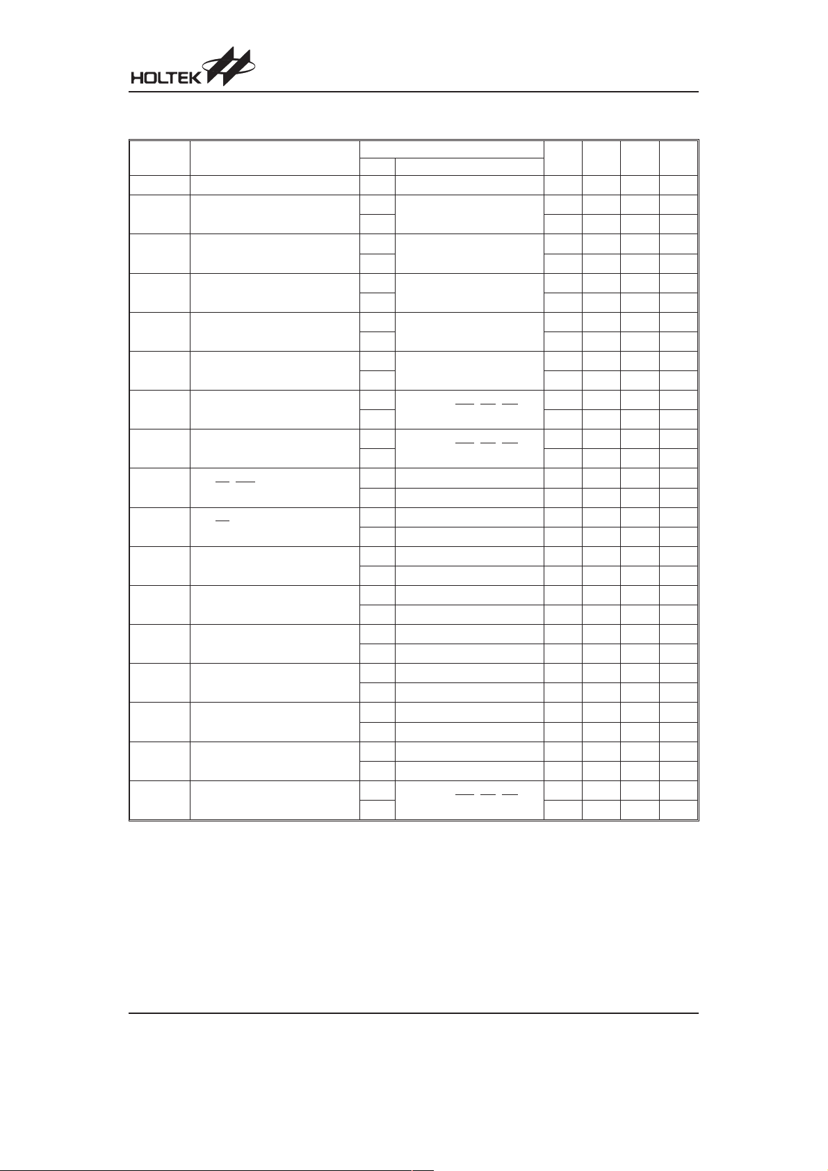
D.C. Characteristics
Symbol Parameter
V
I
DD1
I
DD2
I
DD11
I
DD22
I
STB
V
V
I
OL1
I
OH1
I
OL2
I
OH2
I
OL3
I
OH3
I
OL4
I
OH4
R
DD
IL
IH
PH
Operating Voltage
Operating Current
Operating Current
Operating Current
Operating Current
Standby Current
Input Low Voltage
Input High Voltage
BZ, BZ, IRQ Sink Current
BZ, BZ Source Current
DB0~DB3 Sink Current
DB0~DB3 Source Current
LCD Common Sink Current
LCD Common Source Current
LCD Segment Sink Current
LCD Segment Source Current
Pull-high Resistor
Test Conditions
V
DD
Conditions
¾¾
3V
No load/LCD ON
On-chip RC oscillator
5V
3V
No load/LCD ON
Crystal oscillator
5V
3V
No load/LCD OFF
On-chip RC oscillator
5V
3V
No load/LCD OFF
Crystal oscillator
5V
3V
No load, Power down mode
5V
3V
DB0~DB3, WR,CS,RD
5V 0
3V
DB0~DB3, WR,CS,RD
5V 4.0
V
3V
5V
3V
5V
3V
5V
3V
5V
3V
5V
3V
5V
3V
5V
3V
5V
3V
5V 60 125 210
=0.3V
OL
=0.5V
V
OL
V
=2.7V
OH
=4.5V
V
OH
V
=0.3V
OL
=0.5V
V
OL
V
=2.7V
OH
=4.5V
V
OH
V
=0.3V
OL
=0.5V
V
OL
V
=2.7V
OH
=4.5V
V
OH
V
=0.3V
OL
=0.5V
V
OL
V
=2.7V
OH
=4.5V
V
OH
DB0~DB3, WR,CS,RD
Min. Typ. Max. Unit
2.7
¾
¾
¾
¾
¾
¾
¾
¾
5.2 V
¾
150 250
250 370
135 200
200 300
15 30
50 70
210
310
¾¾
¾¾
0
2.4
¾
¾
¾
0.6 V
1.0 V
¾
1.2 2.5
36
-0.9 -1.8 ¾
-2 -4 ¾
1.2 2.5
36
-0.9 -1.8 ¾
-2 -4 ¾
80 160
180 360
-40 -80 ¾mA
-90 -180 ¾mA
50 100
120 240
-30 -60 ¾mA
-70 -140 ¾mA
150 250 410
Ta=25°C
mA
mA
mA
mA
mA
mA
mA
mA
1
mA
2
mA
3V
5V
mA
¾
mA
¾
mA
mA
mA
¾
mA
¾
mA
mA
¾mA
¾mA
¾mA
¾mA
kW
kW
Rev. 1.30 6 April 13, 2006

HT1660
A.C. Characteristics
Symbol Parameter
f
f
f
f
f
f
t
f
f
t
t
t
t
t
t
t
System Clock
SYS1
System Clock
SYS2
System Clock
SYS3
LCD Frame Frequency
LCD1
LCD Frame Frequency
LCD2
LCD Frame Frequency
LCD3
LCD Common Period
COM
4-Bit Data Clock (WR Pin)
CLK1
4-Bit Data Clock (RD Pin)
CLK2
4-Bit Interface Reset Pulse Width
CS
(Figure 3)
WR,RDInput Pulse Width (Figure 1)
CLK
Rise/Fall Time Serial Data Clock
r,tf
Width (Figure 1)
Setup Time for DB to WR,RDClock
su
Width (Figure 2)
Hold Time for DB to WR,RDClock
h
Width (Figure 2)
Setup Time for CS to WR,RDClock
su1
Width (Figure 3)
Hold Time for CS to WR,RDClock
h1
Width (Figure 3)
Ta=25°C
Test Conditions
V
DD
3V
5V 24 32 40 kHz
Conditions
On-chip RC oscillator
3V
Crystal oscillator
5V
3V
External clock source
5V
3V
On-chip RC oscillator
5V 61/117 89/170 111/213 Hz
3V
Crystal oscillator
5V
3V
External clock source
5V
n: Number of COM
¾
3V
Duty cycle 50%
5V
3V
Duty cycle 50%
5V
CS
¾
Write mode 3.34
3V
Read mode 6.67
Write mode 1.67
5V
Read mode 3.34
3V
5V
¾¾
3V
5V
¾¾
3V
5V
¾¾
3V
5V
¾¾
3V
5V
¾¾
Min. Typ. Max. Unit
22 32 40 kHz
32.768
¾
32.768
¾
¾
¾
32
32
¾
¾
¾
¾
kHz
kHz
kHz
kHz
61/117 89/170 111/213 Hz
n/f
64
64
64
64
LCD
250
¾
¾
¾
¾
¾
sec
150 kHz
300 kHz
75 kHz
150 kHz
¾
¾
¾
¾
¾
¾
¾¾
¾¾
¾¾
¾¾
¾
¾¾ms
¾¾ms
120
120
120
100
100
¾
¾
¾
¾
¾
Hz
Hz
Hz
Hz
ns
ns
ns
ns
ns
ns
Rev. 1.30 7 April 13, 2006

HT1660
W R , R D
C l o c k
t
9 0 %
f
5 0 %
1 0 %
t
C L K
t
r
t
C L K
Figure 1
t
W R , R D
C l o c k
C S
C S
5 0 %
t
5 0 %
F i r s t
C l o c k
t
s u 1
L a s t
C l o c k
h 1
V
G N D
V
G N D
Figure 3
Functional Description
System Oscillator
The HT1660 system clock is used to generate the time
base/Watchdog Timer (WDT) clock frequency, LCD
driving clock, and tone frequency. The clock source
may be from an on-chip RC oscillator (32kHz), a crystal
oscillator (32.768kHz), or an external 32kHz clock by
the S/W setting. The configuration of the system oscilla
tor is as shown. After the SYS DIS command is executed, the system clock will stop and the LCD bias
generator will turn off. That command is available only
for the on-chip RC oscillator or for the crystal oscillator.
Once the system clock stops, the LCD display will become blank, and the time base/WDT loses its function
as well.
V a l i d D a t a
5 0 %
t
s u
t
h
5 0 %
V
G N D
D B
D D
W R , R D
C l o c k
Figure 2
D D
D D
The LCD OFF command is used to turn the LCD bias
generator off. After the LCD bias generator switches off
by issuing the LCD OFF command, using the SYS DIS
command reduces power consumption, thus serving as
a system power down command. But if the external
clock source is chosen as the system clock, using the
SYS DIS command can neither turn the oscillator off nor
carry out the power down mode. The crystal oscillator
option can be applied to connect an external frequency
source of 32kHz to the OSCI pin. In this case, the system fails to enter the power down mode, similar to the
case in the external 32kHz clock source operation. At
the initial system power on, the HT1660 is at the SYS
DIS state.
V
G N D
G N D
D D
O S C I
O S C O
C r y s t a l O s c i l l a t o r
3 2 7 6 8 H z
E x t e r n a l C l o c k S o u r c e
3 2 k H z
S y s t e m
C l o c k
O n - c h i p R C O s c i l l a t o r
3 2 k H z
System Oscillator Configuration
Rev. 1.30 8 April 13, 2006

HT1660
Display Memory - RAM Structure
The static display RAM is organized into 768´4 bits and stores the display data. The contents of the RAM are directly
mapped to the contents of the LCD driver. Data in the RAM can be accessed by the READ, WRITE and
READ-MODIFY-WRITE commands. The following is a mapping from the RAM to the LCD patterns.
00H 08H 10H 18H
COM0 Bit0 Bit0 Bit0 Bit0 Bit0 Bit0
COM1 Bit1 Bit1 Bit1 Bit1 Bit1 Bit1
COM2 Bit2 Bit2 Bit2 Bit2 Bit2 Bit2
COM3 Bit3 Bit3 Bit3 Bit3 Bit3 Bit3
01H 09H 11H 19H
COM4 Bit0 Bit0 Bit0 Bit0 Bit0 Bit0
COM5 Bit1 Bit1 Bit1 Bit1 Bit1 Bit1
COM6 Bit2 Bit2 Bit2 Bit2 Bit2 Bit2
COM7 Bit3 Bit3 Bit3 Bit3 Bit3 Bit3
02H 0AH 12H 1AH
COM8 Bit0 Bit0 Bit0 Bit0 Bit0 Bit0
COM9 Bit1 Bit1 Bit1 Bit1 Bit1 Bit1
COM10 Bit2 Bit2 Bit2 Bit2 Bit2 Bit2
COM11 Bit3 Bit3 Bit03 Bit3 Bit3 Bit3
03H 0BH 13H 1BH
COM12 Bit0 Bit0 Bit0 Bit0 Bit0 Bit0
COM13 Bit1 Bit1 Bit1 Bit1 Bit1 Bit1
COM14 Bit2 Bit2 Bit2 Bit2 Bit2 Bit2
COM15 Bit3 Bit3 Bit3 Bit3 Bit3 Bit3
04H 0CH 14H 1CH
COM16 Bit0 Bit0 Bit0 Bit0 Bit0 Bit0
COM17 Bit1 Bit1 Bit1 Bit1 Bit1 Bit1
COM18 Bit2 Bit2 Bit2 Bit2 Bit2 Bit2
COM19 Bit3 Bit3 Bit3 Bit3 Bit3 Bit3
05H 0DH 15H 1DH
COM20 Bit0 Bit0 Bit0 Bit0 Bit0 Bit0
COM21 Bit1 Bit1 Bit1 Bit1 Bit1 Bit1
COM22 Bit2 Bit2 Bit2 Bit2 Bit2 Bit2
COM23 Bit3 Bit3 Bit3 Bit3 Bit3 Bit3
06H 0EH 16H 1EH
COM24 Bit0 Bit0 Bit0 Bit0 Bit0 Bit0
COM25 Bit1 Bit1 Bit1 Bit1 Bit1 Bit1
COM26 Bit2 Bit2 Bit2 Bit2 Bit2 Bit2
COM27 Bit3 Bit3 Bit3 Bit3 Bit3 Bit3
07H 0FH 17H 1FH
COM28 Bit0 Bit0 Bit0 Bit0 Bit0 Bit0
COM29 Bit1 Bit1 Bit1 Bit1 Bit1 Bit1
COM30 Bit2 Bit2 Bit2 Bit2 Bit2 Bit2
COM31 Bit3 Bit3 Bit3 Bit3 Bit3 Bit3
SEG0 SEG1 SEG2 SEG3 SEG92 SEG93 SEG94 SEG95
96´32 Selection Mode RAM Mapping Table
20H---------2D8H
21H---------2D9H
22H---------2DAH
23H---------2DBH
24H---------2DCH
25H---------2DDH
26H---------2DEH
27H---------2DFH
2E0H 2E8H 2F0H 2F8H
2E1H 2E9H 2F1H 2F9H
2E2H 2EAH 2F2H 2FAH
2E3H 2EBH 2F3H 2FBH
2E4H 2ECH 2F4H 2FCH
2E5H 2EDH 2F5H 2FDH
2E6H 2EEH 2F6H 2FEH
2E7H 2EFH 2F7H 2FFH
Rev. 1.30 9 April 13, 2006

HT1660
00H 04H 08H 0CH
COM0 Bit0 Bit0 Bit0 Bit0 Bit0 Bit0
COM1 Bit1 Bit1 Bit1 Bit1 Bit1 Bit1
COM2 Bit2 Bit2 Bit2 Bit2 Bit2 Bit2
COM3 Bit3 Bit3 Bit3 Bit3 Bit3 Bit3
01H 05H 09H 0DH
COM4 Bit0 Bit0 Bit0 Bit0 Bit0 Bit0
COM5 Bit1 Bit1 Bit1 Bit1 Bit1 Bit1
COM6 Bit2 Bit2 Bit2 Bit2 Bit2 Bit2
COM7 Bit3 Bit3 Bit3 Bit3 Bit3 Bit3
02H 06H 0AH 0EH
COM8 Bit0 Bit0 Bit0 Bit0 Bit0 Bit0
COM9 Bit1 Bit1 Bit1 Bit1 Bit1 Bit1
COM10 Bit2 Bit2 Bit2 Bit2 Bit2 Bit2
COM11 Bit3 Bit3 Bit3s Bit3 Bit3 Bit3
03H 07H 0BH 0FH
COM12 Bit0 Bit0 Bit0 Bit0 Bit0 Bit0
COM13 Bit1 Bit1 Bit1 Bit1 Bit1 Bit1
COM14 Bit2 Bit2 Bit2 Bit2 Bit2 Bit2
COM15 Bit3 Bit3 Bit3 Bit3 Bit3 Bit3
SEG0 SEG1 SEG2 SEG3 SEG108 SEG109 SEG110 SEG111
10H---------1ACH
11H---------1ADH
12H---------1AEH
13H---------1AFH
1B0H 1B4H 1B8H 1BCH
1B1H 1B5H 1B9H 1BDH
1B2H 1B6H 1BAH 1BEH
1B3H 1B7H 1BBH 1BFH
112´16 Selection Mode RAM Mapping Table
Name Command Code Function
112´16 Mode
The default value after power ON reset is 96´32 mode, set ²Normal² command will change 112´16 mode to 96´32
mode.
Frame Frequency
HT1660 provides three kinds of frame frequency option by command code; 64Hz, 89Hz and 170Hz respectively. FRAME
64Hz provides 64Hz frame frequency. FRAME 89Hz provides 89Hz frame frequency. FRAME 170Hz provides 170Hz
frame frequency.
Name Command Code Function
FRAME 170Hz X100-0001-1000-XXXX Select 170Hz frame frequency
FRAME 89Hz X100-0001-1101-XXXX Select 89Hz frame frequency
FRAME 64Hz X100-0001-1110-XXXX Select 64Hz frame frequency
Time Base and Watchdog Timer - WDT
The time base generator and WDT share the same counter which is divided by 256. The IRQ
1Hz, 2Hz, ...., 128Hz output. TIMER DIS/EN/CLR, WDT DIS/EN/CLR and IRQ
Once the WDT time-out occurs, the IRQ
is issued.
If an external clock is selected as the system frequency source, the SYS DIS command turns out invalid and the power
down mode fails to be carried out until the external clock source is removed.
X100-0001-1111-XXXX Change segment from 96 to 112 and common from 32 to 16
Frame Frequency Selection Command Code
clock can be programmed as
EN/DIS are independent from each other.
pin will remain at a logic low level until the CLR WDT or the IRQ DIS command
Rev. 1.30 10 April 13, 2006

HT1660
Buzzer Tone Output
A simple tone generator is implemented in the HT1660.
The tone generator can output a pair of differential driv
ing signals on the BZ and BZ
which are used to generate
a single tone.
By executing the TONE 4K and TONE 2K commands
there are two tone frequency outputs selectable that can
turn on the tone output. The TONE 4K and TONE 2K
commands set the tone frequency to 4kHz and 2kHz, re
spectively. The tone output can be turned off by invoking
the TONE OFF command. The tone outputs, namely BZ
and BZ
, are a pair of differential driving outputs used to
drive a piezo buzzer. Once the system is disabled or the
tone output is inhibited, the BZ and the BZ
outputs will
remain at low level.
Command Format
The HT1660 can be configured by software setting.
There are two mode commands to configure the
HT1660 resource and to transfer the LCD display data.
The configuration mode of the HT1660 is called com
mand mode, and its command mode ID is 100. The
command mode consists of a system configuration
T i m e B a s e
C l o c k S o u r c e
2 5 6
¸
command, a system frequency selection command, an
LCD configuration command, a tone frequency selec
tion command, a bias current selection command, a
timer/WDT setting command, and an operating com
mand. The data mode, on the other hand, includes
READ, WRITE, and READ-MODIFY-WRITE opera
tions.
The following are the data mode ID and the command
mode ID:
-
Operation Mode ID
READ Data 110
WRITE Data 101
READ-MODIFY-WRITE Data 101
COMMAND Command 100
If successive commands have been issued, the com
mand mode ID can be omitted. While the system is op
erating in the non-successive command or the
non-successive address data mode, the CS
be set to ²1² and the previous operation mode will also
be reset. The CS
pin returns to ²0², so a new operation
mode ID should be issued first.
T I M E R E N / D I S
W D T E N / D I S
V
D D
I R Q
-
-
-
-
-
pin should
C L R T i m e r
W D T
4
¸
C L R W D T
Q
D
C K
R
I R Q E N / D I S
Time Base and WDT Configurations
Name Command Code Function
TONE OFF X100-0000-1000-XXXX Turn-off tone output
TONE 4K X100-0001-0000-XXXX Turn-on tone output, tone frequency is 4kHz
TONE 2K X100-0001-0001-XXXX Turn-on tone output, tone frequency is 2kHz
Buzzer Tone Output Command Code
The following are the data mode ID and the command ID:
Operation Mode ID
READ Data 110
WRITE Data 101
READ-MODIFY-WRITE Data 101
COMMAND Command 100
If successivecommands have been issued, the command mode ID can be omitted.While the system is operating in the
non-successive address data mode, the CS
CS
pin returns to 0, so a new operation mode ID should be issued first.
pin should be set 1 and the previous operation mode will also be reset. The
Rev. 1.30 11 April 13, 2006

HT1660
Bias Generator
The HT1660 bias voltage belongs to internal resistor
type. It provides two kinds of bias option named 1/6 bias
and 1/5 bias respectively. It also provides three kinds of
bias current option by programming to suitably drive an
LCD panel. The three kinds of bias current are large,
middle, and small, respectively. Usually, large panel
LCD can be excellently displayed by large bias current.
Relatively, it consumes large current when LCD ON
command is used. Small bias current provides low
power consumption during on condition when the LCD
is normally displayed. The following are the reference
value table.
When the bias current for LCD is more than Large Bias
Current setting. It is recommended to add external cir
cuit to increase driving current.
Interfacing
Only six lines are required to interface with the HT1660.
The CS
line is used to initialize the serial interface circuit
and to terminate the communication between the host
controller and the HT1660. If the CS
pin is set to 1, the
data and command issued between the host controller
and the HT1660 are first disabled and then initialized.
Before issuing a mode command or mode switching, a
high level pulse is required to initialize the serial inter
face of the HT1660. The DB0~DB3 are the 4-bit parallel
data input/output lines. Data to be read or written or
commands to be written have to pass through the
DB0~DB3 lines. The RD
line is the READ clock input.
Data in the RAM are clocked out on the falling edge of the
RD
signal, and the clocked out data will then appear on
the DB0~DB3 lines. It is recommended that the host
controller read correct data during the interval between
the rising edge and the next falling edge of theRD
The WR
dress, and command on the DB0~DB3 lines are all
clocked into the HT1660 on the rising edge of the WR
line is the WRITE clock input. The data, ad
signal. There is an optional IRQ line to be used as an in
terface between the host controller and the HT1660.
The IRQ
pin can be selected as a timer output or a WDT
overflow flag output by the S/W setting. The host con
troller can perform the time base or the WDT function by
connecting with the IRQ
pin of the HT1660.
Bias VLCD Large Bias Current Middle Bias Current Small Bias Current
3V
1/5
5V
3V
1/6
5V
165mA70mA30mA
270mA 110mA50mA
140mA55mA25mA
225mA90mA40mA
-
signal.
-
-
-
P o w e r
V L C D
( T 1 ) V 1
( T 2 ) V 2
V 3
V 4
( T 3 ) V 5
( T 4 ) V 6
V S S
1 / 5 B i a s
V R
R
R
R
R
V
L C D
R
R
R
Internal Resistor Type Bias Generator Configurations
Note: The voltage applied to VLCD pin must be lower than 7V
Adjust VR to fit LCD display
( T 1 ) V 1
( T 2 ) V 2
( T 3 ) V 5
( T 4 ) V 6
V S S
1 / 6 B i a s
P o w e r
V L C D
V 3
V 4
V R
R
R
R
R
V
L C D
R
R
R
Rev. 1.30 12 April 13, 2006

HT1660
V
L C D
V
L C D
R
T 1
R
C
T 2
B i a s
B l o c k
R
C
T 3
R
C
B i a s
B l o c k
T 4
C
R
T 0 0 0
1 / 5 B i a s
1 / 6 B i a s
Increase Driver Current Configurations
Note: The external resistors are used to increment the driving current.
And the external capacitors are used to keep the bias voltage stable.
Timing Diagrams
READ Mode (Command ID Code:110)
C S
V
T 0 0 0
V
L C D
L C D
R
T 1
R
C
T 2
2 R
C
T 3
R
C
T 4
C
R
W R
R D
D 3 D 3 D 3 D 3 D 3 D 3 D 3 D 3 D 3 D 3 D 3 D 3 D 3 D 3 D 3 D 3
A 7 A 3 D 3
D B 3
D B 2
D B 1
D B 0
X X
X
1 A 5 A 1 D 1
A 9
A 8
0 A 4 A 0 D 0
C o m m a n d I D c o d e
( S i n g l e a d d r e s s r e a d i n g )
M e m o r y
A d d r e s s ( M A )
A d d r e s s ( M A )
D a t a ( M A )
X X
1 X
1 A 9
0 A 8
C o m m a n d I D c o d e
A 7 A 3
D 2 D 2 D 2 D 2 D 2 D 2 D 2 D 2 D 2 D 2 D 2 D 2 D 2 D 2 D 2 D 21 A 6 A 2 D 2
A 6 A 2
D 1 D 1 D 1 D 1 D 1 D 1 D 1 D 1 D 1 D 1 D 1 D 1 D 1 D 1 D 1 D 1
A 5 A 1
D 0 D 0 D 0 D 0 D 0 D 0 D 0 D 0 D 0 D 0 D 0 D 0 D 0 D 0 D 0 D 0
A 4 A 0
M e m o r y
A d d r e s s ( M A )
A d d r e s s ( M A )
D a t a ( M A )
D a t a ( M A + 3 )
D a t a ( M A + 2 )
D a t a ( M A + 1 )
( S u c c e s s i v e a d d r e s s r e a d i n g )
D a t a ( M A + 6 )
D a t a ( M A + 5 )
D a t a ( M A + 4 )
D a t a ( M A + 9 )
D a t a ( M A + 8 )
D a t a ( M A + 7 )
D a t a ( M A + 1 2 )
D a t a ( M A + 1 1 )
D a t a ( M A + 1 0 )
D a t a ( M A + 1 5 )
D a t a ( M A + 1 4 )
D a t a ( M A + 1 3 )
Rev. 1.30 13 April 13, 2006

WRITE Mode (Command ID Code:101)
C S
W R
R D
A 7 A 3 D 3
D B 3
D B 2
D B 1
D B 0
X X
X
A 9
0 A 5 A 1 D 1
A 8
1 A 4 A 0 D 0
C o m m a n d I D c o d e
M e m o r y
A d d r e s s ( M A )
A d d r e s s ( M A )
D a t a ( M A )
X X
1 X
0 A 9
1 A 8
C o m m a n d I D c o d e
HT1660
D 3 D 3 D 3 D 3 D 3 D 3 D 3 D 3 D 3 D 3 D 3 D 3 D 3 D 3 D 3 D 3
A 7 A 3
A 6 A 2
D 2 D 2 D 2 D 2 D 2 D 2 D 2 D 2 D 2 D 2 D 2 D 2 D 2 D 2 D 2 D 21 A 6 A 2 D 2
D 1 D 1 D 1 D 1 D 1 D 1 D 1 D 1 D 1 D 1 D 1 D 1 D 1 D 1 D 1 D 1
A 5 A 1
A 4 A 0
A d d r e s s ( M A )
D 0 D 0 D 0 D 0 D 0 D 0 D 0 D 0 D 0 D 0 D 0 D 0 D 0 D 0 D 0 D 0
M e m o r y
A d d r e s s ( M A )
D a t a ( M A + 1 )
D a t a ( M A )
D a t a ( M A + 4 )
D a t a ( M A + 3 )
D a t a ( M A + 2 )
D a t a ( M A + 7 )
D a t a ( M A + 6 )
D a t a ( M A + 5 )
D a t a ( M A + 1 0 )
D a t a ( M A + 9 )
D a t a ( M A + 8 )
D a t a ( M A + 1 5 )
D a t a ( M A + 1 4 )
D a t a ( M A + 1 3 )
D a t a ( M A + 1 2 )
D a t a ( M A + 1 1 )
( S i n g l e a d d r e s s r e a d i n g )
READ-MODIFY-WRITE Mode (Command ID Code:101)
C S
W R
R D
A 7 A 3 D 3
D B 3
D B 2
D B 1
D B 0
X X
X
0
A 9
A 5 A 1 D 1
A 4 A 0 D 0
A 8
1
A d d r e s s ( M A )
C o m m a n d I D c o d e
A d d r e s s ( M A )
( S i n g l e a d d r e s s r e a d i n g )
D 3
D 2
D 1
D 0
D a t a ( M A )
M e m o r y
X X
1 X
0
1
C o m m a n d I D c o d e
A 7 A 3
A 6 A 2
A 5 A 1
A 9
A 4 A 0
A 8
M e m o r y
A d d r e s s ( M A )
A d d r e s s ( M A )
( S u c c e s s i v e a d d r e s s r e a d i n g )
D 3 D 3 D 3 D 3 D 3 D 3 D 3 D 3 D 3 D 3 D 3 D 3 D 3 D 3 D 3 D 3
D 2 D 2 D 2 D 2 D 2 D 2 D 2 D 2 D 2 D 2 D 2 D 2 D 2 D 2 D 2 D 21 A 6 A 2 D 2
D 1 D 1 D 1 D 1 D 1 D 1 D 1 D 1 D 1 D 1 D 1 D 1 D 1 D 1 D 1 D 1
D 0 D 0 D 0 D 0 D 0 D 0 D 0 D 0 D 0 D 0 D 0 D 0 D 0 D 0 D 0 D 0
D a t a ( M A + 1 )
D a t a ( M A )
D a t a ( M A )
D a t a ( M A + 2 )
D a t a ( M A + 2 )
D a t a ( M A + 1 )
( S u c c e s s i v e a d d r e s s r e a d i n g )
D a t a ( M A + 4 )
D a t a ( M A + 3 )
D a t a ( M A + 3 )
D a t a ( M A + 5 )
D a t a ( M A + 5 )
D a t a ( M A + 4 )
D a t a ( M A + 7 )
D a t a ( M A + 6 )
D a t a ( M A + 6 )
D a t a ( M A + 7 )
Rev. 1.30 14 April 13, 2006

Command Mode (Command ID Code:100)
C S
W R
R D
C 4 C 0 X
C o m m a n d
X X
X
X
X
D B 3
D B 2
D B 1
D B 0
X C 7 C 3
1 C 6 C 2 X
0 C 5 C 1 X
0
C o m m a n d I D c o d e
HT1660
C 7 C 3
X
X
C 7 C 3
X
X
C 7 C 3
X
X
C 7 C 3
X
X
X
C 6 C 2
X
X
C 6 C 2
X
1
C 5 C 1
X
X
0
C 4 C 0
0
C o m m a n d I D c o d e
C 5 C 1
X
X
C 4 C 0
C o m m a n d 1
X
C 6 C 2
X
X
C 6 C 2
X
X
C 5 C 1
X
X
C 5 C 1
X
X
C 4 C 0
X
X
C o m m a n d 2
C 4 C 0
C o m m a n d 3
C 7 C 3
X
X
C 6 C 2
X
X
C 5 C 1
X
X
C 4 C 0
C o m m a n d 4
C o m m a n d 5
( S i n g l e c o m m a n d )
Note: ²X² stands for don¢t care
Application Circuits
Host Controller With an HT1660 Display System
*
M C U
*
R
C l o c k O u t
E x t e r n a l C l o c k 1 ( 3 2 k H z )
E x t e r n a l C l o c k 2 ( 3 2 k H z )
O n - c h i p O S C
C r y s t a l
3 2 7 6 8 H z
( S u c c e s s i v e c o m m a n d )
C S
R D
W R
D B 0 ~ D B 3
H T 1 6 6 0
I R Q
O S C I
O S C O
C O M 0 ~ C O M 3 1 S E G 0 ~ S E G 9 5
* 1 / 6 B i a s o r 1 / 5 B i a s ,
1 / 3 2 D u t y o r 1 / 1 6 D u t y
* L C D P a n e l
V L C D
M a x .
7 V
*
V R
B Z
P i e z o
B Z
The connection of IRQ
*Note:
and RD pin can be selected depending on the MCU.
Adjust VR to fit LCD display
Adjust R (external pull-high resistance) to fit user¢s time base clock.
It is recommended that the internal equivalent capacitance between SEG and COM of LCD panel should be
lower than 10pF. (LCR meter test condition: frequency in 1KHz)
Rev. 1.30 15 April 13, 2006

HT1660
Instruction Set Summary
Name Command Code D/C Function Def.
READ
WRITE
READ-MODIFYWRITE
SYS DIS X100-0000-0000-XXXX-XXXX C
SYS EN X100-0000-0001-XXXX-XXXX C Turn On system oscillator
LCD OFF X100-0000-0010-XXXX-XXXX C Turn Off LCD display Yes
LCD ON X100-0000-0011-XXXX-XXXX C Turn On LCD display
TIMER DIS X100-0000-0100-XXXX-XXXX C Disable time base output Yes
WDT DIS X100-0000-0101-XXXX-XXXX C Disable WDT time-out flag output Yes
TIMER EN X100-0000-0110-XXXX-XXXX C Enable time base output
WDT EN X100-0000-0111-XXXX-XXXX C Enable WDT time-out flag output
TONE OFF X100-0000-1000-XXXX-XXXX C Turn Off tone outputs Yes
CLR TIMER X100-0000-1101-XXXX-XXXX C Clear the contents of thetime base generator
CLR WDT X100-0000-1111-XXXX-XXXX C Clear the contents of the WDT stage
TONE 4K X100-0001-0000-XXXX-XXXX C
TONE 2K X100-0001-0001-XXXX-XXXX C
IRQ DIS X100-0001-0010-XXXX-XXXX C Disable IRQ
IRQ EN X100-0001-0011-XXXX-XXXX C Enable IRQ
RC 32K X100-0001-0100-XXXX-XXXX C System clock source, on-chip RC oscillator Yes
EXT (X¢TAL)
LARGE BIAS X100-0001-0110-XXXX-XXXX C Large bias current option Yes
MIDDLE BIAS X100-0001-0111-XXXX-XXXX C Middle bias current option
SMALL BIAS X100-0001-1000-XXXX-XXXX C Small bias current option
BIAS 1/6 X100-0001-1010-XXXX-XXXX C LCD 1/6 bias option Yes
BIAS 1/5 X100-0001-1001-XXXX-XXXX C LCD 1/5 bias option
FRAME 170Hz X100-0001-1100-XXXX-XXXX C Selects 170Hz frame frequency
FRAME 89Hz X100-0001-1101-XXXX-XXXX C Selects 89Hz frame frequency
FRAME 64Hz X100-0001-1110-XXXX-XXXX C Selects 64Hz frame frequency Yes
Select 112´16
F1 X100-1010-0000-XXXX-XXXX C
F2 X100-1010-0001-XXXX-XXXX C
F4 X100-1010-0010-XXXX-XXXX C
X110-XXA9A8-A7A6A5A4-A3A2A1A0D3D2D1D0
X101-XXA9A8-A7A6A5A4-A3A2A1A0D3D2D1D0
X101-XXA9A8-A7A6A5A4-A3A2A1A0D3D2D1D0
X100-0001-0101-XXXX-XXXX C
X100-0001-1111-XXXX-XXXX C
D Read data from the RAM
D Write data to the RAM
D Read and Write data to the RAM
Turn Off both system oscillator and LCD bias
generator
Turn on tone output, tone frequency output:
4kHz
Turn on tone output, tone frequency output:
2kHz
output Yes
output
System clock source, external 32kHz clock
source or crystal oscillator 32.768kHz
This command will change segment from 96
to 112 and command from 32 to 16
Time base clock output: 1Hz
The WDT time-out flag after: 4s
Time base clock output: 2Hz
The WDT time-out flag after: 2s
Time base clock output: 4Hz
The WDT time-out flag after: 1s
Yes
Rev. 1.30 16 April 13, 2006

Name Command Code D/C Function Def.
F8 X100-1010-0011-XXXX-XXXX C
F16 X100-1010-0100-XXXX-XXXX C
F32 X100-1010-0101-XXXX-XXXX C
F64 X100-1010-0110-XXXX-XXXX C
F128 X100-1010-0111-XXXX-XXXX C
TEST X100-1111-1111-XXXX-XXXX C
NORMAL X100-1111-1110-XXXX-XXXX C
Note:
²X² stands for don¢t care
A9~A0: RAM address
D3~D0: RAM data
D/C: Data/Command mode
Def.: Power-on reset default
All the bold forms, namely 110, 101, and 100, are mode commands. Of these, 100 indicates the command
mode ID. If successive commands have been issued, the command mode ID except for the first command will
be omitted. The tone frequency source and the time base/WDT clock frequency source can be derived from an
on-chip 32kHz RC oscillator, a 32.768kHz crystal oscillator, or an external 32kHz clock. Calculation of the fre
quency is based on the system frequency sources as stated above. It is recommended that the host controller
should initialize the HT1660 after power-on reset, otherwise, power on reset may fail, which in turn leads to the
malfunctioning of the HT1660.
Time base clock output: 8Hz
The WDT time-out flag after: 1/2s
Time base clock output: 16Hz
The WDT time-out flag after: 1/4s
Time base clock output: 32Hz
The WDT time-out flag after: 1/8s
Time base clock output: 96Hz
The time-out flag after: 1/16s
Time base clock output: 128Hz
The WDT time-out flag after: 1/32s
Test mode, user don¢t use.
Normal mode, 96´32 mode will be set
HT1660
Yes
Yes
-
Rev. 1.30 17 April 13, 2006

Package Information
208-pin QFP (28´28) Outline Dimensions
1 5 6
1 5 7
A B
HT1660
C
D
1 0 5
1 0 4
F
H
G
I
2 0 8
1
Symbol
Min. Nom. Max.
Dimensions in mm
A31
B 27.9
C31
D 27.9
E
F
¾
¾
G 3.1
H
I
¾¾
¾
J 0.35
K 0.1
5 2
¾
¾
¾
¾
0.5
0.2
¾
0.1
¾
¾
5 3
a 0°¾7°
E
a
K
J
31.4
28.1
31.4
28.1
¾
¾
3.4
3.7
¾
0.65
0.2
Rev. 1.30 18 April 13, 2006

Holtek Semiconductor Inc. (Headquarters)
No.3, Creation Rd. II, Science Park, Hsinchu, Taiwan
Tel: 886-3-563-1999
Fax: 886-3-563-1189
http://www.holtek.com.tw
Holtek Semiconductor Inc. (Taipei Sales Office)
4F-2, No. 3-2, YuanQu St., Nankang Software Park, Taipei 115, Taiwan
Tel: 886-2-2655-7070
Fax: 886-2-2655-7373
Fax: 886-2-2655-7383 (International sales hotline)
HT1660
Holtek Semiconductor Inc. (Shanghai Sales Office)
7th Floor, Building 2, No.889, Yi Shan Rd., Shanghai, China 200233
Tel: 021-6485-5560
Fax: 021-6485-0313
http://www.holtek.com.cn
Holtek Semiconductor Inc. (Shenzhen Sales Office)
5/F, Unit A, Productivity Building, Cross of Science M 3rd Road and Gaoxin M 2nd Road, Science Park, Nanshan District,
Shenzhen, China 518057
Tel: 0755-8616-9908, 8616-9308
Fax: 0755-8616-9533
Holtek Semiconductor Inc. (Beijing Sales Office)
Suite 1721, Jinyu Tower, A129 West Xuan Wu Men Street, Xicheng District, Beijing, China 100031
Tel: 010-6641-0030, 6641-7751, 6641-7752
Fax: 010-6641-0125
Holtek Semiconductor Inc. (Chengdu Sales Office)
709, Building 3, Champagne Plaza, No.97 Dongda Street, Chengdu, Sichuan, China 610016
Tel: 028-6653-6590
Fax: 028-6653-6591
Holmate Semiconductor, Inc. (North America Sales Office)
46729 Fremont Blvd., Fremont, CA 94538
Tel: 510-252-9880
Fax: 510-252-9885
http://www.holmate.com
Copyright Ó 2006 by HOLTEK SEMICONDUCTOR INC.
The information appearing in this Data Sheet is believed to be accurate at the time of publication. However, Holtek as
sumes no responsibility arising from the use of the specifications described. The applications mentioned herein are used
solely for the purpose of illustration and Holtek makes no warranty or representation that such applications will be suitable
without further modification, nor recommends the use of its products for application that may present a risk to human life
due to malfunction or otherwise. Holtek¢s products are not authorized for use as critical components in life support devices
or systems. Holtek reserves the right to alter its products without prior notification. For the most up-to-date information,
please visit our web site at http://www.holtek.com.tw.
-
Rev. 1.30 19 April 13, 2006
 Loading...