


4-Level Gray Scale 64´16 LCD Controller for I/O mC
Features
Operating voltage: 2.7V~5.2V
·
Built-in 32kHz RC oscillator
·
External 32.768kHz crystal oscillator or
·
32kHz frequency source input
Standby current < 1mAat3V,<2mAat5V
·
Internal resistor type: 1/5 bias or 1/4
·
bias, 1/16 duty
Two selectable LCD frame frequencies:
·
89Hz or 170Hz
Max. 64´16 patterns, 64 segments and 16
·
commons
Built-in bit-map display RAM: 2048 bits
·
(=64´16´2 bits)
Built-in internal resistor type bias generator
·
Six-wire interface (four data wires)
·
Eight kinds of time base/WDT selection
·
Time base or WDT overflow output
·
R/W address auto increment
·
Applications
Toys
·
Games
·
Personal digital assistant
·
HT1647
Built-in buzzer driver (2kHz/4kHz)
·
Power down command reduces power
·
consumption
Software configuration feature
·
Data mode and Command mode
·
instructions
Three data accessing modes
·
Provides VLCD pin to adjust LCD operating
·
voltage
Provides three kinds of bias current
·
programming
Control of TN-type, STN-type LCDs and
·
ECB-type LCDs
Four-level gray scale output for TN-type,
·
STN-type LCDs panel
Four-color output for ECB-type LCDs panel
·
Available in 100-pin QFP and in chip form
·
Cellular phone
·
Global positioning system
·
Consumer electronics
·
General Description
HT1647 is a peripheral device specially designed for I/O type mC used to expand the display capability. The max. display segment of
the device are 1024 patterns (64 segments and
16 commons). It also supports four data bits in
terface, buzzer sound, Watchdog Timer or time
base timer functions. The HT1647 is a memory
mapping and multi-function LCD controller.
Since the HT1647 can control ECB-type (Elec
trically Controlled Birefringence) LCDs in ad
dition to current TN-type (Twisted Nematic) or
STN-type (Super Twisted Nematic) LCDs, it
can support 4-color display as well as 4-level
gray scale display. It displays 4-level gray scale
output when HT1647 drives TN-type,
STN-type LCDs. It displays four color output
when HT1647 drives ECB-type. HT1647 uses
PWM (Pulse Width Modulation) technique. The
software configuration feature of the HT1647
make it suitable for multiple LCD applications
including LCD modules and display subsys
tems. Only six lines (CS
required for the interface between the host con
troller and the HT1647. The HT164X series
have many kinds of products that match vari
ous applications.
1 April 21, 2000
,WR, DB0~DB3) are
-
-
-
4-Level Gray Scale LCD Controller Product Line Selection Table
HT164X *HT1642 *HT1645 HT1647
COM 88
SEG 32 64
*Under development
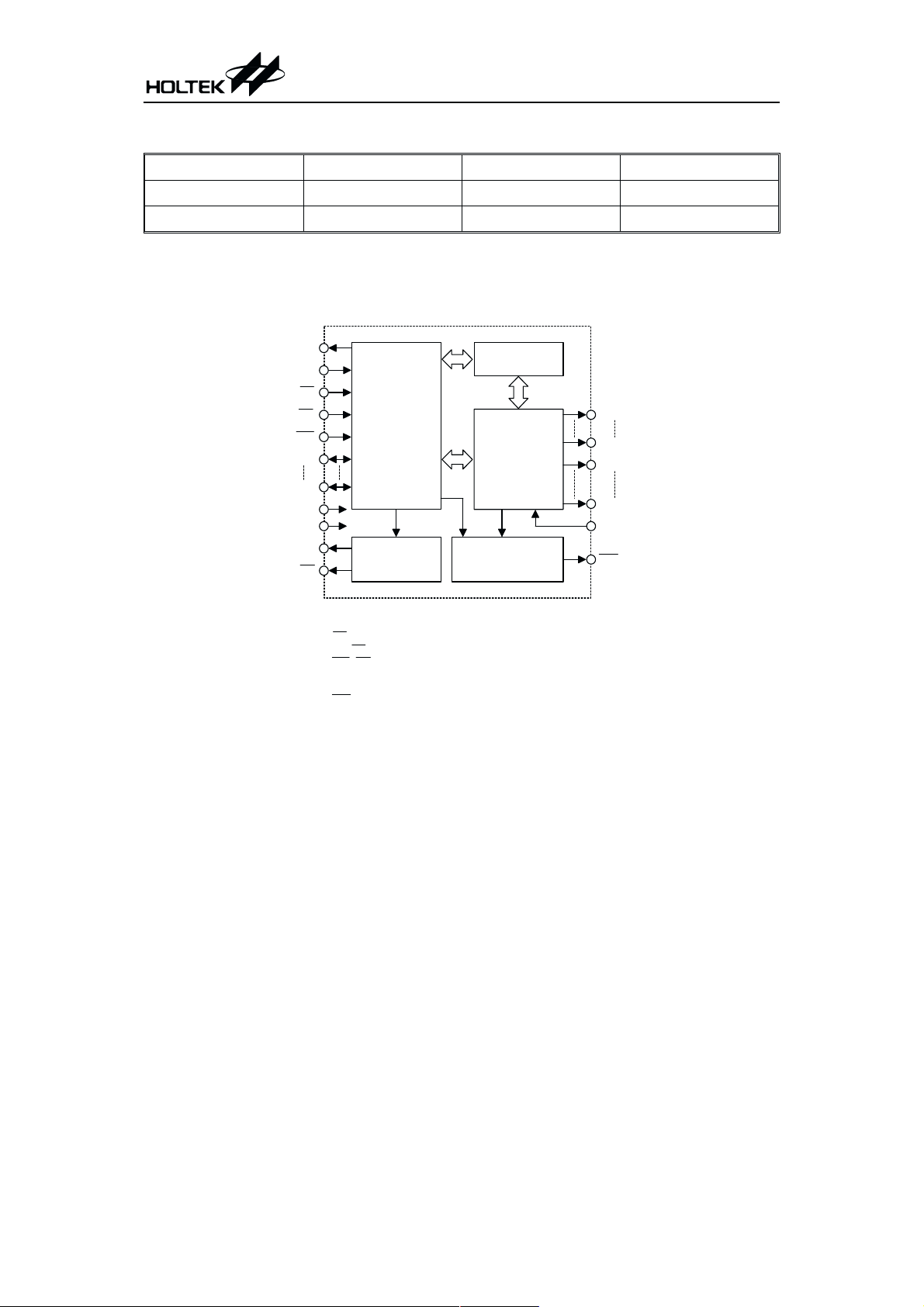
Block Diagram
HT1647
16
64
OSCO
OSCI
CS
RD
WR
DB0
DB3
VDD
VSS
BZ
BZ
N ote: C S : C hip selection
Tone Frequency
G enerator
BZ, B Z: Tone outputs
W R, RD: W RITE clock, READ clock
D B 0~D B3: D ata bus
C O M 0~C O M 15, S E G 0~S EG 63: LC D outputs
IR Q : Tim e base or W D T overflow output
C ontrol
&
Tim ing
Circuit
D ispla y R A M
LC D D river/
Bias Circuit
W atchdog Tim er
Tim e Base G enerator
&
COM 0
COM 15
SEG 0
SEG 63
VLCD
IR Q
2 April 21, 2000
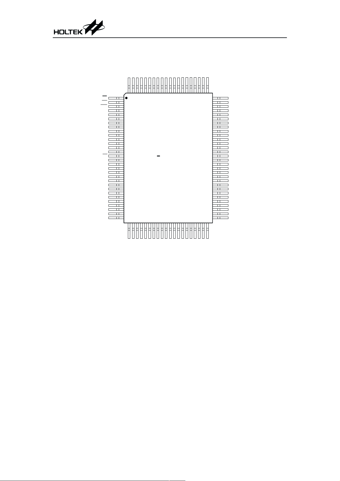
Pin Assignment
HT1647
SEG 44
SEG 45
SEG 46
SEG 47
SEG 48
SEG 49
SEG 50
SEG 51
SEG 52
SEG 53
SEG 54
SEG 55
SEG 56
SEG 57
SEG 58
SEG 59
SEG 60
SEG 61
SEG 62
SEG 63
CS
RD
WR
DB0
DB1
DB2
DB3
VSS
OSCI
OSCO
VDD
VLCD
IR Q
BZ
BZ
T1
T2
T3
T4
NC
COM 0
COM 1
COM 2
COM 3
COM 4
COM 5
COM 6
COM 7
COM 8
COM 9
1
H T1647
100 Q FP
30
31 50
COM 10
COM 11
COM 12
COM 13
COM 14
COM 15
SEG 0
SEG 1
SEG 2
SEG 4
SEG 5
SEG 6
SEG 7
SEG 8
SEG 9
SEG 10
SEG 11
SEG 3
SEG 12
81100
80
51
SEG 13
SEG 43
SEG 42
SEG 41
SEG 40
SEG 39
SEG 38
SEG 37
SEG 36
SEG 35
SEG 34
SEG 33
SEG 32
SEG 31
SEG 30
SEG 29
SEG 28
SEG 27
SEG 26
SEG 25
SEG 24
SEG 23
SEG 22
SEG 21
SEG 20
SEG 19
SEG 18
SEG 17
SEG 16
SEG 15
SEG 14
3 April 21, 2000
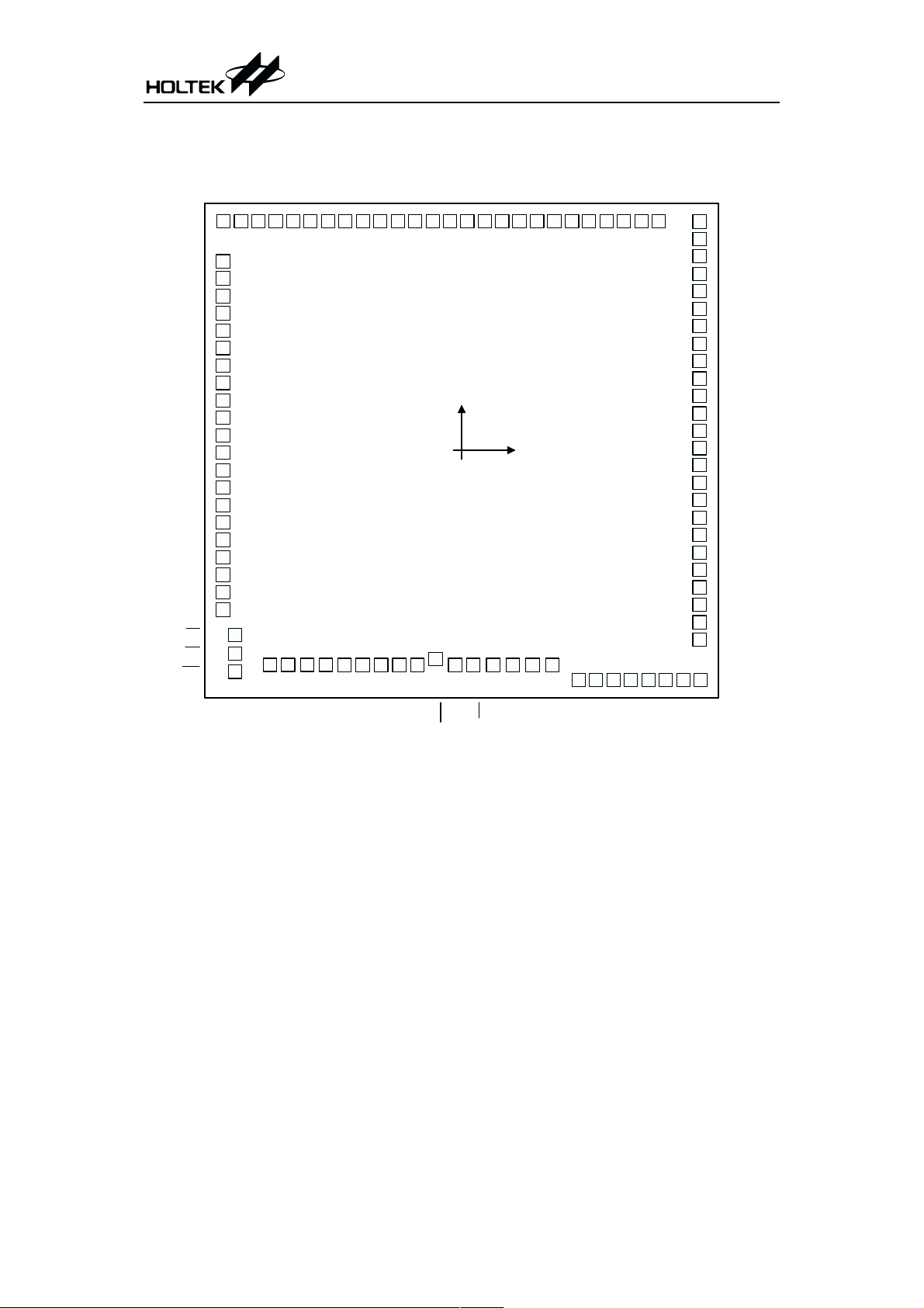
Pad Assignment
SEG 40
SEG 41
HT1647
SEG 17
SEG 18
SEG 19
SEG 20
SEG 22
SEG 24
SEG 25
SEG 26
SEG 27
SEG 28
SEG 29
SEG 30
SEG 31
SEG 32
SEG 33
SEG 34
SEG 35
SEG 36
SEG 37
SEG 38
SEG 39
SEG 21
SEG 23
SEG 42
SEG 43
SEG 44
SEG 45
SEG 46
SEG 47
SEG 48
SEG 49
SEG 50
SEG 51
SEG 52
SEG 53
SEG 54
SEG 55
SEG 56
SEG 57
SEG 58
SEG 59
SEG 60
SEG 61
SEG 62
SEG 63
CS
RD
WR
1
2
3
4
5
6
7
8
9
10
11
12
13
14
15
16
17
18
19
20
21
22
99
23
24
25
26762777287829
DB0
DB1
DB2
74
75
73
72
71
70
69
68
67
66
65
64
63
62
61
60
59
58
57
56
55
54
53
52
51
50
4494459546964797489849
COM 2
COM 3
COM 6
COM 5
COM 4
SEG 16
SEG 15
SEG 14
SEG 13
SEG 12
SEG 11
SEG 10
SEG 9
SEG 8
SEG 7
SEG 6
SEG 5
SEG 4
SEG 3
SEG 2
SEG 1
SEG 0
COM 15
COM 14
COM 13
COM 12
COM 11
COM 10
COM 9
COM 8
COM 7
T4
7930803181328233833484358536863787
COM 0
COM 1
9142924393
(0 , 0 )
38883989409041
DB3
VSS
OSCI
OSCO
VDD
VLCD
BZ
IR Q
BZ
T1T3T2
Chip size: 3865 ´ 3770 (mm)
2
* The IC substrate should be connected to VSS in the PCB layout artwork.
4 April 21, 2000

HT1647
Pad Coordinates
Pad No. X Y Pad No. X Y Pad No. X Y
10
11
12
13
14
15
16
17
18
19
20
21
22
23
24
25
26
27
28
29
30
31
32
33
1
-1774.50
2
-1779.30
3
-1779.30
4
-1779.30
5
-1779.30
6
-1779.30
7
-1779.30
8
-1779.30
9
-1779.30
-1779.30
-1779.30
-1779.30
-1779.30 -17.20
-1779.30 -149.00
-1779.30 -277.00
-1779.30 -408.80
-1779.30 -536.80
-1779.30 -668.60
-1779.30 -796.60
-1779.30 -928.80
-1779.30 -1056.80
-1779.30 -1189.00
-1690.00 -1375.40
-1690.00 -1515.40
-1690.00 -1651.00
-1430.20 -1599.90
-1294.80 -1599.90
-1149.50 -1599.90
-1013.90 -1599.90
-872.80 -1600.00
-738.30 -1600.00
-600.10 -1600.00
-465.60 -1600.00
1708.30 34
1409.80 35
1281.80 36
1150.00 37 87.40
1022.00 38 235.20
890.20 39 383.40
762.20 40 530.40
630.40 41 678.60
502.40 42 875.00
370.60 43 1003.00
242.60 44 1134.80
110.80 45 1262.80
46 1394.60
47 1522.60
48 1654.40
49 1782.40
50 1775.70
51 1775.70
52 1775.70
53 1775.70
54 1775.70
55 1775.70
56 1775.70
57 1775.70
58 1775.70
59 1775.70
60 1775.70
61 1775.70 15.90 94
62 1775.70 147.70 95
63 1775.70 275.70 96
64 1775.70 407.50 97
65 1775.70 535.50 98
66 1775.70 667.30 99
-331.40 -1600.00
-194.50 -1558.30
-48.00 -1600.00
-1600.00
-1600.00
-1600.00
-1600.00
-1600.00
-1712.30
-1712.30
-1712.30
-1712.30
-1712.30
-1712.30
-1712.30
-1712.30
-1411.10
-1283.10
-1151.30
-1023.30
-891.50
-763.50
-631.70
-503.70
-371.90
-243.90
-112.10
67 1775.70 795.30
68 1775.70 927.10
69 1775.70 1055.10
70 1775.70 1186.90
71 1775.70 1314.90
72 1775.70 1446.70
73 1775.70 1574.70
74 1775.70 1706.50
75 1471.10 1708.30
76 1343.10 1708.30
77 1211.30 1708.30
78 1083.30 1708.30
79 951.50 1708.30
80 823.50 1708.30
81 691.70 1708.30
82 563.70 1708.30
83 431.90 1708.30
84 303.90 1708.30
85 172.10 1708.30
86 44.10 1708.30
87
88
89
90
91
92
93
-87.70
-215.70
-347.50
-475.50
-607.30
-735.30
-867.10
-995.10
-1126.90
-1254.90
-1386.70
-1514.70
-1646.50
1708.30
1708.30
1708.30
1708.30
1708.30
1708.30
1708.30
1708.30
1708.30
1708.30
1708.30
1708.30
1708.30
Unit: mm
5 April 21, 2000
HT1647
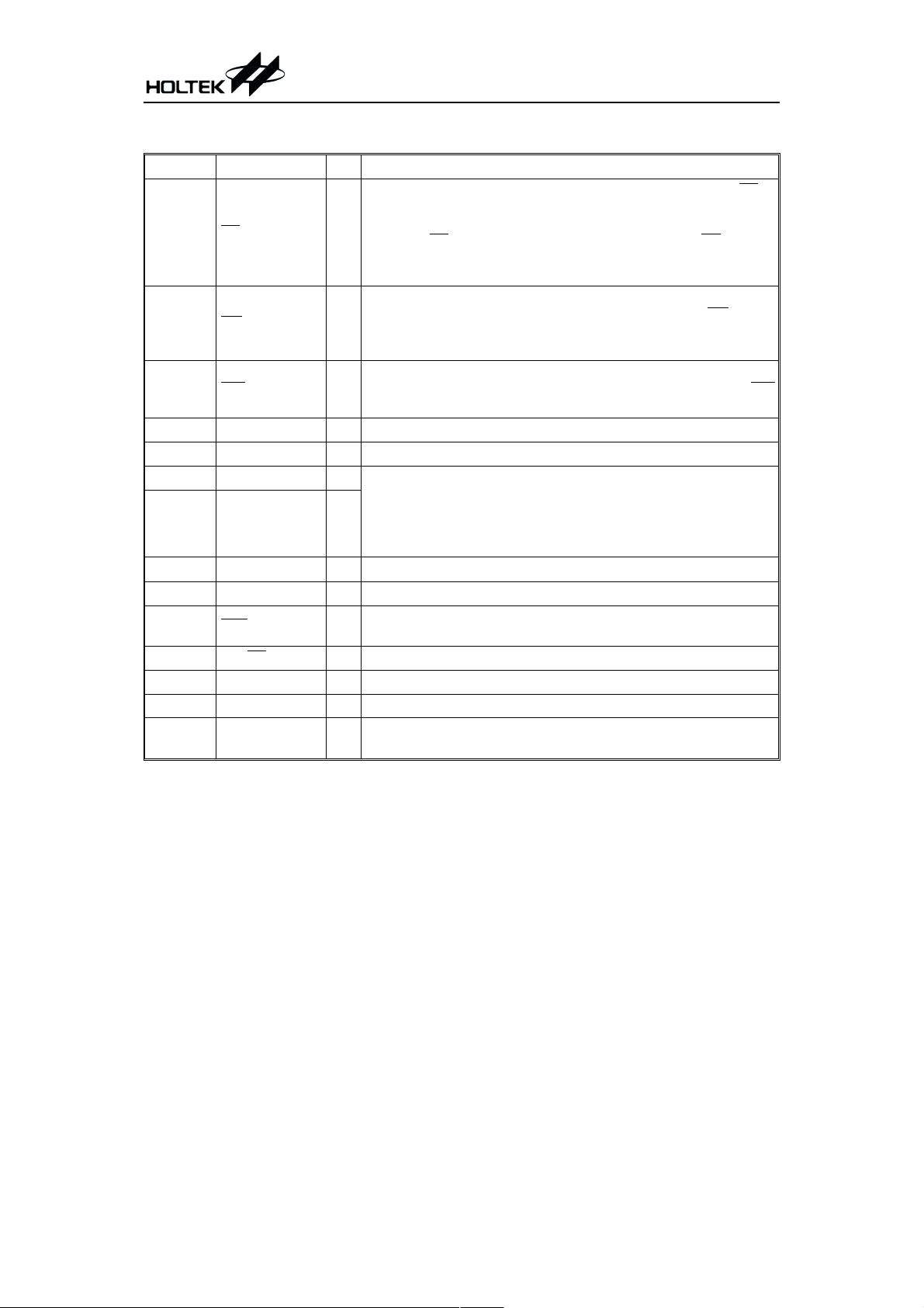
Pad Description
Pad No. Pad Name I/O Description
Chip selection input with pull-high resistor. When the CS
logic high, the data and command read from or write to the
HT1647 are disabled. The serial interface circuit is also reset.
23 CS
24 RD
25 WR
26~29 DB0~DB3 I/O Parallel data input/output with a pull-high resistor
30 VSS
31 OSCI I The OSCI and OSCO pads are connected to a 32.768kHz crystal
32 OSCO O
33 VDD
34 VLCD I Power supply for LCD driver circuit
35 IRQ
36, 37 BZ, BZ
38~41 T1~T4 I Not connected
42~57 COM0~COM15 O LCD common outputs
58~99,
1~22
SEG0~SEG63 O LCD segment outputs
I
But if the CS
data and command transmission between the host controller
and the HT1647 are all enabled.
READ clock input with pull-high resistor. Data in the RAM of
the HT1647 are clocked out on the rising edge of the RD
I
The clocked out data will appear on the data line. The host con
troller can use the next falling edge to latch the clocked out data.
WRITE clock input with pull-high resistor. Data on the DATA
I
line are latched into the HT1647 on the rising edge of the WR
signal.
Negative power supply for logic circuit, ground
¾
in order to generate a system clock. If the system clock comes
from an external clock source, the external clock source should
be connected to the OSCI pad. But if an on-chip RC oscillator is
selected instead, the OSCI and OSCO pads can be left open.
Positive power supply for logic circuit
¾
Time base or Watchdog Timer overflow flag, NMOS open drain
O
output.
O 2kHz or 4kHz frequency output pair (tristate output buffer)
is at a logic low level and is input to the CS pad, the
is
signal.
-
Absolute Maximum Ratings
Supply Voltage..............................-0.3V to 5.5V
Input Voltage ................V
Note: These are stress ratings only. Stresses exceeding the range specified under ²Absolute Maxi
mum Ratings² may cause substantial damage to the device. Functional operation of this device
at other conditions beyond those listed in the specification is not implied and prolonged expo
sure to extreme conditions may affect device reliability.
-0.3V to VDD+0.3V
SS
Storage Temperature.................-50°Cto125°C
Operating Temperature ..............-25°Cto75°C
6 April 21, 2000
-
-
HT1647
D.C. Characteristics
Symbol Parameter
V
DD
I
DD1
I
DD2
I
DD11
I
DD22
I
STB
V
IL
V
IH
I
OL1
I
OH1
I
OL2
I
OH2
I
OL3
I
OH3
I
OL4
I
OH4
R
PH
Operating Voltage
Operating Current
Operating Current
Operating Current
Operating Current
Standby Current
Input Low Voltage
Input High Voltage
BZ, BZ, IRQ Sink Current
BZ, BZ Source Current
DB0~DB3 Sink Current
DB0~DB3 Source Current
LCD Common Sink Current
LCD Common Source Current
LCD Segment Sink Current
LCD Segment Source Current
Pull-high Resistor
Test Conditions
V
DD
Conditions
¾¾
3V
No load/LCD ON
On-chip RC oscillator
5V
3V
No load/LCD ON
Crystal oscillator
5V
3V
No load/LCD OFF
On-chip RC oscillator
5V
3V
No load/LCD OFF
Crystal oscillator
5V
3V
No load
Power down mode
5V
3V
DB0~DB3, WR
RD
5V 0
3V
DB0~DB3, WR
RD
5V 4.0
V
3V
5V
3V
5V
3V
5V
3V
5V
3V
5V
3V
5V
3V
5V
3V
5V
3V
5V 60 125 180
=0.3V
OL
=0.5V
V
OL
V
=2.7V
OH
V
=4.5V
OH
V
=0.3V
OL
=0.5V
V
OL
V
=2.7V
OH
V
=4.5V
OH
V
=0.3V
OL
=0.5V
V
OL
V
=2.7V
OH
V
=4.5V
OH
V
=0.3V
OL
=0.5V
V
OL
V
=2.7V
OH
V
=4.5V
OH
DB0~DB3, WR
RD
,CS,
,CS,
,CS,
Min. Typ. Max. Unit
2.7
¾
150 250
¾
250 370
¾
135 200
¾
200 300
¾
15 30
¾
50 70
¾
210
¾
310
¾
¾¾
¾¾
0
¾
¾
2.4
¾
¾
1.2 2.5
36
-0.9 -1.8 ¾
-2 -4 ¾
1.2 2.5
36
-0.9 -1.8 ¾
-2 -4 ¾
50 100
100 200
-25 -50 ¾mA
-50 -100 ¾mA
30 60
60 120
-20 -40 ¾mA
-35 -70 ¾mA
150 250 350
Ta=25°C
5.2 V
mA
mA
A
m
mA
mA
mA
mA
mA
1
mA
2
mA
0.6 V
1.0 V
3V
5V
mA
¾
mA
¾
mA
mA
mA
¾
mA
¾
mA
mA
¾mA
¾mA
¾mA
¾mA
kW
kW
7 April 21, 2000
HT1647
A.C. Characteristics
Symbol Parameter
f
SYS1
f
SYS2
f
SYS3
f
LCD1
f
LCD2
f
LCD3
t
COM
f
CLK1
f
CLK2
t
CS
t
CLK
t
r,tf
t
su
t
h
t
su1
t
h1
System Clock
System Clock
System Clock
LCD Frame Frequency
LCD Frame Frequency
LCD Frame Frequency
LCD Common Period
4-Bit Data Clock (WR Pin)
4-Bit Data Clock (RD Pin)
4-Bit Interface Reset Pulse
Width (Figure 3)
WR,RDInput Pulse Width
Rise/Fall Time Serial Data
Clock Width (Figure 1)
Setup Time for DB to WR,
RD
Clock Width (Figure 2)
Hold Time for DB to WR,RD
Clock Width (Figure 2)
Setup Time for CS to WR,RD
Clock Width (Figure 3)
Hold Time for CS to WR,RD
Clock Width (Figure 3)
(Figure 1)
Ta=25°C
Test Conditions
V
DD
3V
5V 24 32 40 kHz
3V
5V
3V
5V
3V
5V 48 64 80 Hz
3V
5V
3V
5V
¾
3V
5V
3V
5V
¾
3V
5V
3V
5V
3V
5V
3V
5V
3V
5V
3V
5V
Conditions
On-chip RC oscillator
Crystal oscillator
External clock source
On-chip RC oscillator
Crystal oscillator
External clock source
n: Number of COM
Duty cycle 50%
Duty cycle 50%
CS
Write mode 3.34
Read mode 6.67
Write mode 1.67
Read mode 3.34
¾¾
¾¾
¾¾
¾¾
¾¾
Min. Typ. Max. Unit
22 32 40 kHz
¾
¾
¾
¾
32.768
32.768
32
32
¾
¾
¾
¾
kHz
kHz
kHz
kHz
44 64 80 Hz
64
¾
64
¾
64
¾
64
¾
n/f
¾
¾¾
¾¾
¾¾
¾¾
250
¾
LCD
¾
¾
¾
¾
¾
150 kHz
300 kHz
75 kHz
150 kHz
¾
¾¾ms
¾¾ms
120
120
120
100
100
¾
¾
¾
¾
¾
Hz
Hz
Hz
Hz
sec
ns
ns
ns
ns
ns
ns
8 April 21, 2000

HT1647
WR, RD
Clock
90%
50%
10%
t
f
t
CLK
t
r
t
CLK
Figure 1
t
CS
WR, RD
Clock
50%
FIR ST
Clock
50%
CS
t
LAST
Clock
h1
t
su1
V
GND
V
GND
Figure 3
Functional Description
System oscillator
The HT1647 system clock is used to generate
the time base/Watchdog Timer (WDT) clock fre
quency, LCD driving clock, and tone frequency.
The source of the clock may be from an on-chip
RC oscillator (32kHz), a crystal oscillator
(32.768kHz), or an external 32kHz clock by the
S/W setting. The configuration of the system oscillator is as shown. After the SYS DIS command is executed, the system clock will stop
and the LCD bias generator will turn off. That
command is, however, available only for the
on-chip RC oscillator or for the crystal oscillator. Once the system clock stops, the LCD display will become blank, and the time base/WDT
loses its function as well.
VALID DATA
50%
t
su
50%
t
h
V
DD
GND
W R , R D
Clock
DB
Figure 2
DD
DD
The LCD OFF command is used to turn the
LCD bias generator off. After the LCD bias gen
-
erator switches off by issuing the LCD OFF
command, using the SYS DIS command re
duces power consumption, serving as a system
power down command. But if the external clock
source is chosen as the system clock, using the
SYS DIS command can neither turn the oscillator off nor carry out the power down mode. The
crystal oscillator option can be applied to connect an external frequency source of 32kHz to
the OSCI pin. In this case, the system fails to
enter the power down mode, similar to the case
in the external 32kHz clock source operation.
At the initial system power on, the HT1647 is at
the SYS DIS state.
V
DD
GND
GND
-
-
OSCI
OSCO
C rystal O scillator
32768H z
E xte rna l C lo ck S ource
32kHz
O n-chip R C O scillator
32kHz
System oscillator configuration
9 April 21, 2000
S yste m
Clock

HT1647
Display memory - RAM structure
The static display RAM is organized into 512´4
bits and stores the display data. Two bits of
RAM map to Lad¢s one pixel and decide
whether 4-level gray scale or 4-color display
COM 14COM 15
SEG 0
SEG 1
SEG 2
SEG 3
SEG 63
D0D1D2D3
7
15
23
31
511
Addr
Data
Data 4 Bits
(D 3, D 2, D 1, D 0)
: Tw o bits of R AM m ap to LC D 's one pixel and decide 4-level gray scale
or 4-color display concurrently.
concurrently. The contents of the RAM are di
rectly mapped to the contents of the LCD
driver. Data in the RAM can be accessed by the
READ, WRITE and READ-MODIFY-WRITE
commands. The following is a mapping from
the RAM to the LCD patterns.
COM 0COM 1
0
8
16
Address 9 B its
24
(A 8 , A 7 , ...., A 0 )
504
D0
Addr
Data
D1D2D3
-
Display memory - RAM structure
Gray scale level decision
HT1647 uses PWM technique to provide 4-level
gray scale display. Two bits of RAM data code
((D3, D2) or (D1, D0)) decide one pixel level of
LCDs, level 1~level 4 dividedly. Every level
must be defined as one kind of gray scale by PWM
data (namely B4~B0) previously.
RAM data code
(D3, D2) or (D1, D0)
Choice Gray Scale
Level
(1, 1) Level 1
(1, 0) Level 2
(0, 1) Level 3
(0, 0) Level 4
RAM data defined gray scale level
Frame frequency
HT1647 provides two kinds frame frequency option by command code, 89Hz and 170Hz respectively. FRAME 89Hz provides 89Hz frame
frequency and active segment signal width can be
divided into 24 sections concurrently. FRAME
170Hz provides 170Hz frame frequency and ac
tive segment signal width can be divided into 13
sections concurrently. The 24 sections display a
particularly gray scale more than the 13 sections
by PWM data. The default is FRAME 89Hz.
Gray scale display
If the user choose 89Hz frame frequency, a max.
of 24 sections can be programmed to suit a sat
isfactory gray scale in every level. Similarly, if
the user choose 170Hz frame frequency, a max.
of 13 sections can be programmed to suit a satis
10 April 21, 2000
-
-
-

Name Command Code Function
FRAME 170Hz
FRAME 89Hz
X100-0001-1000-XXXX
X100-0001-1101-XXXX
Frame frequency selection command code
Select 170Hz frame frequency and active segment
signal width can be divided into 13 sections
Select 89Hz frame frequency and active segment sig
nal width can be divided into 24 sections
HT1647
-
factory gray scale in every level. HT1647 provides
5-bit PWM data to control the length of the sec
tion. In other words, a max. 24 gray scales are gen
erated by 5-bit binary PWM data. At FRAME
89Hz mode, the HT1647 only provides a max. of
24 adjustable gray scales although 32 is the ex
pressed max. value by 5 bits binary code. When 5
bits binary code value is more than 23, the PWM
control circuit uniformly regards 23. To increase
PWM data indicates to increase the length of the
active segment signal. The varied length of the ac
tive segment signal displays varied gray scale in
Name Command Code Function
GRS LEVEL 1
GRS LEVEL 2
GRS LEVEL 3
GRS LEVEL 4
X100-001 B4-B3 B2 B1 B0-XXXX
X100-010 B4-B3 B2 B1 B0-XXXX
X100-011 B4-B3 B2 B1 B0-XXXX
X100-100 B4-B3 B2 B1 B0-XXXX
Four kinds of gray scale level command code
TN-type, STN-type LCDs (refer to table 1). Simi
larly, it displays varied color in ECB-type LCDs.
The color display is derived from ECB-type LCD
specification. At FRAME 170Hz mode, the
HT1647 only provides a max. of 13 adjustable
gray scales although 32 is the expressed max.
value by 5 bits binary code. When the 5 bits bi
nary code value is more than 12, the PWM con
trol circuit uniformly regards 12. The user must
appoint four kinds of PWM data to four kinds of
different gray scale level by commanding PWM
data (refer to table 2).
Set PWM data in gray scale level 1
Set PWM data in gray scale level 2
Set PWM data in gray scale level 3
Set PWM data in gray scale level 4
-
-
-
11 April 21, 2000

HT1647
COM
V
LC D
V1
V2
V3
V4
V
SS
16 1 2
16 1 2
W
W'
SEG
V
LC D
V1
V2
V3
V4
V
SS
W'
W
ON
COM ~SEG
3/5V
1/5V
-1 /5 V
-3 /5 V
V
LC D
LC D
LC D
LC D
LC D
-V
LC D
ONOFF
1 fram e
N ote: "W '" R eal active segm ent signal w idth (adjustable w idth by P W M data)
"W " M a x . a c tiv e s e g m e n t s ig n a l w id th
<
P W M (O N w id th ): W '/W , 0 W '/W 1 ( re fe r to ta b le 1 & tabel 2)
<
Example of waveform (B type) in 1/5 bias, 1/16 duty cycle drive
12 April 21, 2000

HT1647
Time base and Watchdog Timer - WDT
The time base generator and WDT share the
same divided (/256) counter. The IRQ
clock can be
programmed as 1Hz, 2Hz, ...., 128Hz output.
TIMER DIS/EN/CLR, WDT DIS/EN/CLR and
IRQ
EN/DIS are independent from each other.
Once the WDT time-out occurs, the IRQ
Tim e Base
C lock S o urce
/256
CLR Tim er
pin will
WDT
/4
CLR W DT
remain at a logic low level until the CLR WDT
or the IRQ
DIS command is issued.
If an external clock is selected as the system
frequency source, the SYS DIS command turns
out invalid and the power down mode fails to be
carried out until the external clock source is re
moved.
TIM ER E N /D IS
W D T E N /D IS
V
DD
Q
D
CK
R
IR Q E N /D IS
Time base and WDT configurations
Buzzer tone output
A simple tone generator is implemented in the
HT1647. The tone generator can output a pair
of differential driving signals on the BZ and BZ
which are used to generate a single tone.
By executing the TONE 4K and TONE 2K commands there are two tone frequency outputs
selectable and turn on tone output. The TONE
4K and TONE 2K commands set the tone fre
quency to 4kHz and 2kHz, respectively. The
tone output can be turned off by invoking the
TONE OFF command. The tone outputs,
namely BZ and BZ
driving outputs used to drive a piezo buzzer.
Once the system is disabled or the tone output
is inhibited, the BZ and the BZ
main at low level.
Name Command Code Function
TONE OFF
TONE 4K
TONE 2K
X100-0000-1000-XXXX
X100-0001-0000-XXXX
X100-0001-0001-XXXX
Turn-off tone output
Turn-on tone output, tone frequency is 4kHz
Turn-on tone output, tone frequency is 2kHz
-
IR Q
-
, are a pair of differential
outputs will re-
Buzzer tone output command code
Command format
The HT1647 can be configured by software set
ting. There are two mode commands to config
ure the HT1647 resource and to transfer the
LCD display data.
The configuration mode of the HT1647 is called
command mode, and its command mode ID is
100. The command mode consists of a system
configuration command, a system frequency se
lection command, an LCD configuration com
mand, a tone frequency selection command, a
bias current selection command, a gray scale
level selection command, a timer/WDT setting
command, and an operating command. The
data mode, on the other hand, includes READ,
WRITE, and READ-MODIFY-WRITE opera
tions.
13 April 21, 2000
-
-
-

HT1647
The following are the data mode ID and the
command mode ID:
Operation Mode ID
READ Data 110
WRITE Data 101
READ-MODIFY-WRITE Data 101
COMMAND Command 100
If successive commands have been issued, the
command mode ID can be omitted. While the
system is operating in the non-successive com
mand or the non-successive address data mode,
pin should be set to ²1² and the previous
the CS
operation mode will also be reset. The CS
pin
returns to ²0², so a new operation mode ID
should be issued first.
Bias generator
The HT1647 bias voltage belong to internal re
sistor type. It provides two kinds of bias option
named 1/5 bias and 1/4 bias respectively. It is
recommeaded to select 1/5 bias to fit TN-type,
STN-type LCDs and select 1/4 bias to fit
ECB-type LCDs. It also provides three kinds of
bias current option by programming to suitably
drive LCD panel. The three kinds of bias cur
rent are large, middle, and small, respectively.
Usually, large panel LCD can be excellently dis
played by large bias current. Relatively, it con
sumes large current when LCD ON command is
used. Small bias current provides low power
consumption during on condition when the
LCD is normally displayed. The following are
the reference value table.
VLCD Bias Large bias current Middle bias current Small bias current
4V 1/5
4V 1/4
300mA 100mA40mA
375mA 125mA50mA
VDD
VLCD
V1
V2
V3
V4
VSS
1/5 bias
*
VR
R
R
*
R
V
LC D
R
R
VDD
VLCD
V1
V2
V3
V4
VSS
1/4 bias
*
VR
R
R
*
R
V
LC D
R
R
-
-
-
-
* The voltage applied to V
p in m u s t b e lo w e r th a n V
LC D
DD
* A d ju s t V R to fit L C D d is p la y , a t V DD= 5 V , V LC D= 4 V , V R = 1 5 kW 2 0 %
Internal resistor type bias generator configurations
14 April 21, 2000

HT1647
Interfacing
Only six lines are required to interface with the
HT1647. The CS
line is used to initialize the se
rial interface circuit and to terminate the commu
nication between the host controller and the
HT1647. If the CS
pin is set to 1, the data and
command issued between the host controller and
the HT1647 are first disabled and then initial
ized. Before issuing a mode command or mode
switching, a high level pulse is required to initial
ize the serial interface of the HT1647. The
DB0~DB3 are the 4-bit parallel data input/out
put lines. Data to be read or written or commands
to be written have to pass through the DB0~DB3
lines. The RD
line is the READ clock input. Data
Relationship table between PWM data and
gray scale
5 b its P W M d a ta
Value
B4 B3 B2 B1 B0
0
0
1
0
2
0
3
0
4
0
0
5
0
6
0
7
0
8
0
9
0
10
0
11
0
12
0
13
0
14
0
15
1
16
1
17
1
18
1
19
1
20
1
21
1
22
1
23
1
24
000
0
0
0
0
1
0
0
1
0
0
0
1
0
0
1
0
1
1
0
1
1
0
0
0
1
0
0
1
1
0
1
1
0
1
0
1
1
0
1
1
1
1
1
1
1
1
0
0
0
0
0
0
1
0
0
1
0
0
0
1
0
0
1
0
1
0
1
1
0
1101010
(O N w idth)
1
0
1
0
1
0
1
0
1
0
10/23
1
11/23
0
12/23
1
13/23
0
14/23
1
15/23
0
16/23
1
17/23
0
18/23
1
19/23
0
20/23
1
21/23
01
22/23
1
PW M
0 (0/23)
1/23
2/23
3/23
4/23
5/23
6/23
7/23
8/23
9/23
1 (23/23)
1 (24/23)
G ray Scale
in the RAM are clocked out on the falling edge of
the RD
appear on the DB0~DB3 lines. It is recommended
that the host controller read in correct data dur
ing the interval between the rising edge and the
next falling edge of the RD
signal, and the clocked out data will then
signal. The WR line is
the WRITE clock input. The data, address, and
command on the DB0~DB3 lines are all clocked
into the HT1647 on the rising edge of the WR
nal. There is an optional IRQ
interface between the host controller and the
HT1647. The IRQ
output or a WDT overflow flag output by the S/W
pin can be selected as a timer
line to be used as an
setting. The host controller can perform the time
base or the WDT function by connecting with the
IRQ
pin of the HT1647.
Frame 89Hz mode (table 1)
5 b its PW M data
Value
B4 B3 B2 B1 B0
0
0
1
0
2
0
3
0
4
0
0
5
0
6
0
7
0
8
0
9
0
10
0
11
0
12
0
13
1
31
0
0
0
0
0
0
0
1
1
1
1
111
1 1 1 1
1
0
1
0
1
0
1
0
1
1
1
1
0
0
0
0
0
1
0
1
1
0
000
0
0
0
(O N w idth)
1
0
1
0
1
0
1
0
1
10/12
0
11/12
1
1 (12/12)
010
1 (13/12)
PW M
0 (0/12)
1/12
2/12
3/12
4/12
5/12
6/12
7/12
8/12
9/12
1 (31/12)
N ote: The varied PW M data display varied
g ra y s c a le in T N -ty p e , S T N -ty p e L C D s .
T h e c o lo r d is p la y d e riv e s fro m E C B -ty p e
L C D 's s p e c ific a tio n .
G ray Scale
sig
-
-
1
31
1
1 (31/23)
15 April 21, 2000

Timing Diagrams
READ mode (command ID code:110)
CS
WR
RD
HT1647
DB3
DB2
DB1
DB0
A8 A7A3D3
A6 A2 D 2
1
A5A1D1
1
A4 A0 D0
0
C om m and ID code
(S ingle address reading) (S uccessive address reading)
Data (MA)
Memory
Address (M A )
A7 A3 D3 D3A8D3 D3 D3 D3 D3 D3 D3 D3 D3 D3 D3 D3 D3 D3
A6 A2 D2 D21D2 D2 D2 D2 D2 D2 D2 D2 D2 D2 D2 D2 D2 D2
A5 A1 D1 D11D1 D1 D1 D1 D1 D1 D1 D1 D1 D1 D1 D1 D1 D1
A4 A0 D0 D00D0 D0 D0 D0 D0 D0 D0 D0 D0 D0 D0 D0 D0 D0
Memory
Address (M A )
C om m and ID code
Data (MA+2)
Data (MA+1)
Data (MA)
Data (MA+5)
Data (MA+4)
Data (MA+3)
Data (MA+8)
Data (MA+7)
Data (MA+6)
D ata (M A +15)
D ata (M A +14)
D ata (M A +13)
D ata (M A +12)
D ata (M A +11)
D ata (M A +10)
Data (MA+9)
16 April 21, 2000

WRITE mode (command ID code:101)
CS
WR
RD
A8 A7
A3
DB3
D3
HT1647
A7 A3 D3 D3A8 D3 D3 D3 D3 D3 D3 D3 D3 D3 D3 D3 D3 D3 D3
DB2
DB1
DB0
A6 A2 D 2
0A5A1
1A4A0 D0
C om m and ID code
(S ingle address w riting) (S uccessive address w riting)
D1
Data (M A)
Memory
Address (M A )
A6 A2 D2 D21D2 D2 D2 D2 D2 D2 D2 D2 D2 D2 D2 D2 D2 D21
A5 A1 D 1 D10D1 D1 D1 D1 D1 D1 D1 D1 D1 D1 D1 D1 D1 D1
A4 A0 D0 D01D0 D0 D0 D0 D0 D0 D0 D0 D0 D0 D0 D0 D0 D0
Memory
Address (M A )
C om m and ID code
Data (M A+2)
Data (M A+1)
Data (M A)
Data (M A+5)
Data (M A+4)
Data (M A+3)
Data (M A+8)
Data (M A+7)
Data (M A+6)
D ata (M A +15)
D ata (M A +14)
D ata (M A +13)
D ata (M A +12)
D ata (M A +11)
D ata (M A +10)
Data (M A+9)
17 April 21, 2000

READ-MODIFY-WRITE mode (command ID code:101)
CS
WR
RD
HT1647
DB3
DB2
DB1
DB0
A8 A7 A3
1A6A2D2
0A5A1D1
1A4A0D0
C om m and ID code
(S in gle add ress acce ssin g) (S ucce ssive a dd ress acce ssing )
D3
D3
D2
D1
D0
Data (M A)
Memory
Address (M A )
Data (M A)
A7 A3
D3A8D3 D3 D3 D3 D3 D3 D3 D3 D3 D3 D3 D3 D3
A6 A2 D 21D2 D2 D2 D2 D2 D2 D2 D2 D2 D2 D2 D2 D2
A5 A1 D10D1 D1 D1 D1 D1 D1 D1 D1 D1 D1 D1 D1 D1
A4 A0 D01D0 D0 D0 D0 D0 D0 D0 D0 D0 D0 D0 D0 D0
Data (M A)
Memory
Address (M A )
C om m and ID code
Data (M A+1)
Data (M A)
Data (M A+2)
Data (M A+1)
Data (M A+3)
Data (M A+2)
Data (M A+3)
Data (M A+4)
Data (M A+5)
Data (M A+4)
Data (M A+6)
Data (M A+6)
Data (M A+5)
18 April 21, 2000

Command mode (command ID code:100)
CS
WR
RD
HT1647
DB3
DB2
DB1
DB0
XC8C4C0
1C7C3X
0C6C2X
0
C5 C1 X
C om m and ID code
C om m and
(S ingle com m and)
Note: ²X² stands for don¢t care
C8 C4 C0 C8X C4C0C8C4C0C8C4C0C8C4C0C8C4C0
1
C7 C3 X
0
C6 C2 X C6 C2 X
C5 C1 X C5 C1 X
0
C om m and ID code
C om m and 1
C7 C3 X
C7 C3 X C7 C3 X C7 C3 X C7 C3
C6 C2 X C6 C2 X C6 C2 X C6 C2
C5 C1 X C5 C1 X C5 C1 X C5 C1
C om m and 2
(S uccessive com m and)
C om m and 3
C om m and 4
C om m and 5
X
X
X
C om m and 6
19 April 21, 2000

Application Circuits
Host controller with an HT1647 display system
*
m
C
*
R
C lock O ut
External C lock 1 (32kHz)
External C lock 2 (32kHz)
O n-chip O SC
C rysta l
32768H z
CS
RD
WR
DB0~DB3
IR Q
OSCI
OSCO
C O M 0 ~ C O M 1 5 S E G 0 ~ S E G 6 3
*1/5 B ias (or 1/4 B ias), 1/16 D uty
H T1647
LCD Panel
VDD
VLCD
BZ
BZ
HT1647
*
VR
Piezo
*Note:
The connection of IRQ
The voltage applied to V
Adjust VR to fit LCD display, at V
and RD pin can be selected depending on the mC.
pin must be lower than VDD.
LCD
=5V, V
DD
=4V, VR=15kW±20%.
LCD
It is recommended toselect 1/5 bias to fitTN-type, STN-type LCDs and select 1/4 bias to fitm
ECB-type LCDs.
Adjust R (external pull high resistance) to fit user¢s time base clock.
20 April 21, 2000

HT1647
Instruction Set Summary
Name Command Code D/C Function Def.
READ
WRITE
READMODIFYWRITE
SYS DIS
SYS EN
LCD OFF
LCD ON
TIMER DIS
WDT DIS
TIMER EN
WDT EN
TONE OFF
CLR
TIMER
CLR WDT
TONE 4K
TONE 2K
IRQ DIS
IRQ EN
RC 32K
EXT
(XTAL)
LARGE
BIAS
MIDDLE
BIAS
A8110-A7A6A5A4A3A2A1A0D3D2D1D0
A8101-A7A6A5A4A3A2A1A0D3D2D1D0
A8101-A7A6A5A4A3A2A1A0D3D2D1D0
X100-0000-0000-XXXX
X100-0000-0001-XXXX
X100-0000-0010-XXXX
X100-0000-0011-XXXX
X100-0000-0100-XXXX
X100-0000-0101-XXXX
X100-0000-0110-XXXX
X100-0000-0111-XXXX
X100-0000-1000-XXXX
X100-0000-1101-XXXX
X100-0000-1111-XXXX
X100-0001-0000-XXXX
X100-0001-0001-XXXX
X100-0001-0010-XXXX
X100-0001-0011-XXXX
X100-0001-0100-XXXX
X100-0001-0101-XXXX
X100-0001-0110-XXXX
X100-0001-0111-XXXX
D Read data from the RAM
D Write data to the RAM
D Read and Write data to the RAM
Turn Off both system oscillator
C
and LCD bias generator
C Turn On system oscillator
C Turn Off LCD display Yes
C Turn On LCD display
C Disable time base output Yes
C Disable WDT time-out flag output Yes
C Enable time base output
C Enable WDT time-out flag output
C Turn Off tone outputs Yes
Clear the contents of the time base
C
generator
Clear the contents of the WDT
C
stage
Turn on tone output, tone
C
frequency output: 4kHz
Turn on tone output, tone
C
frequency output: 2kHz
C Disable IRQ
C Enable IRQ
System clock source, on-chip RC
C
oscillator
System clock source, external
C
32kHz clock source or crystal
oscillator 32.768kHz
C Large bias current option Yes
C Middle bias current option
output Yes
output
Yes
Yes
21 April 21, 2000

HT1647
Name Command Code D/C Function Def.
SMALL
BIAS
BIAS 1/5
BIAS 1/4
FRAME
170Hz
FRAME
89Hz
GRS
LEVEL1
GRS
LEVEL2
GRS
LEVEL3
GRS
LEVEL4
F1
F2
F4
F8
F16
F32
F64
F128
TEST
NORMAL
X100-0001-1000-XXXX
X100-0001-1001-XXXX
X100-0001-1010-XXXX
X100-0001-1100-XXXX
X100-0001-1101-XXXX
X100-001 B4-B3 B2 B1 B0-XXXX
X100-010 B4-B3 B2 B1 B0-XXXX
X100-011 B4-B3 B2 B1 B0-XXXX
X100-100 B4-B3 B2 B1 B0-XXXX
X100-1010-0000-XXXX
X100-1010-0001-XXXX
X100-1010-0010-XXXX
X100-1010-0011-XXXX
X100-1010-0100-XXXX
X100-1010-0101-XXXX
X100-1010-0110-XXXX
X100-1010-0111-XXXX
X100-1111-1111-XXXX
X100-1111-1110-XXXX
C Small bias current option
C LCD 1/5 bias option Yes
C LCD 1/4 bias option
Select 170Hz frame frequency
C
and active segment signal width
can be divided 13 sections
Select 89Hz frame frequency
C
and active segment signal width
can be divided 24 sections
C Set PWM data in gray scale level 1
C Set PWM data in gray scale level 2
C Set PWM data in gray scale level 3
C Set PWM data in gray scale level 4
Time base clock output: 1Hz
C
The WDT time-out flag after: 4s
Time base clock output: 2Hz
C
The WDT time-out flag after: 2s
Time base clock output: 4Hz
C
The WDT time-out flag after: 1s
Time base clock output: 8Hz
C
The WDT time-out flag after: 1/2 s
Time base clock output: 16Hz
C
The WDT time-out flag after: 1/4 s
Time base clock output: 32Hz
C
The WDT time-out flag after: 1/8 s
Time base clock output: 64Hz
C
The WDT time-out flag after: 1/16 s
Time base clock output: 128Hz
C
The WDT time-out flag after: 1/32 s
C
Test mode, user don¢t use.
C Normal mode Yes
Yes
Yes
22 April 21, 2000

Note:
²X² stands for don¢t care
A8~A0 : RAM address
D3~D0 : RAM data
B4~B0 : PWM data
D/C : Data/Command mode
Def. : Power-on reset default
All the bold forms, namely 110, 101, and 100, are mode commands. Of these, 100indicates
the command mode ID. If successive commands have been issued, the command mode ID ex
cept for the first command will be omitted. The source of the tone frequency and of the time
base/WDT clock frequency can be derived from an on-chip 32kHz RC oscillator, a 32.768kHz
crystal oscillator, or an external 32kHz clock. Calculation of the frequency is based on the sys
tem frequency sources as stated above. It is recommended that the host controller should ini
tialize the HT1647 after power-on reset, for power on reset may fail, which in turn leads to the
malfunctioning of the HT1647.
HT1647
-
-
-
23 April 21, 2000

HT1647
Holtek Semiconductor Inc. (Headquarters)
No.3 Creation Rd. II, Science-based Industrial Park, Hsinchu, Taiwan, R.O.C.
Tel: 886-3-563-1999
Fax: 886-3-563-1189
Holtek Semiconductor Inc. (Taipei Office)
5F, No.576, Sec.7 Chung Hsiao E. Rd., Taipei, Taiwan, R.O.C.
Tel: 886-2-2782-9635
Fax: 886-2-2782-9636
Fax: 886-2-2782-7128 (International sales hotline)
Holtek Semiconductor (Hong Kong) Ltd.
RM.711, Tower 2, Cheung Sha Wan Plaza, 833 Cheung Sha Wan Rd., Kowloon, Hong Kong
Tel: 852-2-745-8288
Fax: 852-2-742-8657
Copyright ã 2000 by HOLTEK SEMICONDUCTOR INC.
The information appearing in this Data Sheet is believed to be accurate at the time of publication. However, Holtek
assumes no responsibility arising from the use of thespecifications described. The applications mentioned herein are
used solely for the purpose of illustration and Holtek makes no warranty or representation that such applications
will be suitable without further modification, nor recommends the use of its products for application that may pres
ent a risk to human life due to malfunction or otherwise. Holtek reserves the right to alter its products without prior
notification. For the most up-to-date information, please visit our web site at http://www.holtek.com.tw.
24 April 21, 2000
-
 Loading...