


Features
·
Operating voltage: 2.4V~3.5V
·
33 common/120 segment LCD driver output
·
33´120=3960 bits capacity of built-in graphic display
data RAM (BGDRAM)
·
Master and slave mode available for multi-chip
operation
·
8-bit Parallel interface with general MCU
·
On-chip oscillator circuit for display clock, external
clock can also be used
·
Selectable multiplex ratio: 1/16, 1/32, 1/33
·
Selectable bias ratio: 1/5 or 1/7
·
External driving circuit for external bias supply
·
On-chip selectable voltage doublers and tripler
·
Wide rangeof operating temperature: -30°Cto85°C
·
S/W controlled electronic contrast control function
(16 levels)
General Description
The HT0610 is a driver and controller LSI for graphic
dot-matrix liquid crystal display systems. It has 33 common and 120 segment driver circuits. This chip is connected directly to an MCU, accepts 8-bit parallel display
data and stores an on-chip graphic display data RAM
(BGDRAM) of 33´120 bits. It provides a high-flexible
display section due to the one-to-one correspondence
HT0610
33´120 LCD Driver
·
External contrast control
·
Low power icon mode driven by com32
·
Four static icon driver circuit
·
High accuracy voltage regulator with temperature co
efficient (0.00%, -0.18%, -0.22%, -0.35%)
·
Low power consumption
-
Read/write mode 170mA (Typical)
-
Display mode 160mA (Typical)
-
Standby mode 15mA (Typical; Display off; internal
oscillator enable)
-
Standby mode < 1mA (Typical; Display off; external
oscillator enable)
·
CMOS process
·
TCP available
between BGDRAM bits and LCD panel pixels. It per
forms BGDRAM read/write operation with no externally
operating clock to minimize power consumption. In addition, because it contains power supply circuits necessary to drive an LCD, it is possible to make a display
system with minimal components.
-
-
Rev. 1.10 1 April 4, 2007
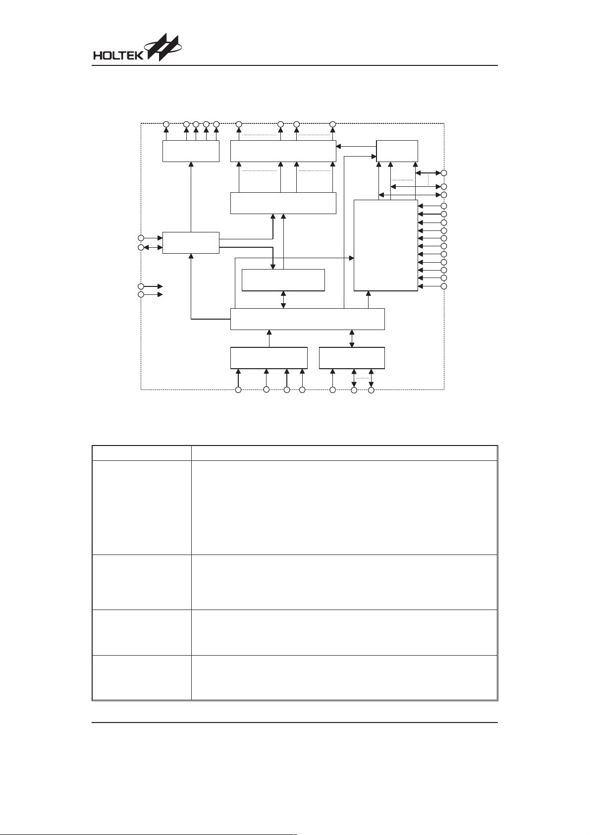
Block Diagram
HT0610
O S C 1
O S C 2
V D D
V S S
I B P
I C O
N 0 ~ I C O N 3
S t a t i c I c o n
C o n t r o l C i r c u i t
T i m i n g G e n e r a t o r
f o r D i s p l a y
S E G 0 ~ S E G 1 1 9
H i g h V o l t a g e C e l l L e v e l S h i f t e r
1 5 5 B i t s L a t c h
( 3 3 B i t s & 1 2 0 B i t s )
B G D R A M
1 2 0
3 3 B i t s
´
C o m m a n d D e c o d e r C i r c u i t
C o m m a n d I n t e r f a c e
C S ( C L K )
D C O M
R E S
C O M 0 ~ C O M 3 2
P a r a l l e l I n t e r f a c e
C E
L e v e l
S e l e c t o r
V L L 2
V L L 6
V C C A 1
L C D D r i v i n g
V o l t a g e G e n e r a t o r
D o u b l e r & T r i p l e r
V o l t a g e R e g u l a t o r ,
V o l t a g e D i v
C o n t r a s t C o n t r o l ,
T e m p e r a t u r e
C o m p e n s a t i o n
R W
D 0 ~ D 7
i d e r ,
C i r c u i t
V R
V F
C 2 P
C 2 N
C 1 P
C 1 N
D U M 2
D U M 1
C +
C V D D A
Operation of LCD Driver
Description of Block Diagram Module
Block Description
This module determines whether the input data is interpreted as data or command.
Data is directed to this module based upon the input of the DCOM pin. If DCOM High,
then data is written to BGDRAM ( Built-in Graphic Display data RAM). DCOM pin Low
Command Decoder and
Command Interface
Parallel Interface
Built-in Graphic Display
data RAM (BGDRAM)
Display Timing Generator
indicates that the input at D0~D7 is interpreted as a Command.
CE is the master chip selection signal. A High input enable the input lines ready to sam
ple signals.
RES pin of same function as Power On Reset (POR). Once RES received the reset sig
nal, all internal circuitry will back to its initial status. Refer to Command Description
section for more information.
The parallel interface consists of 8 bi-directional data lines (D0~D7), RW and CS. The
RW input High indicates a read operation from the BGDRAM. RW input Low indicates a
write to BGDRAM or Internal Command Registers depending on the status of DCOM
pin input.
The CS input serves as data latch signal (clock).
The BGDRAM is a bit mapped static RAM holding the bit pattern to be displayed. The
size of the BGDRAM is determined by number of row times the number of column
(120´33 =3960 bits). Figure as followis a description of the BGDRAM address map. For
mechanical flexibility, re-mapping on both segment and common outputs are provided.
This module is an on chip low power RC oscillator circuitry. The oscillator frequency can
be selected in the range of 15kHz to 50kHz by external resistor. One can enable the cir
cuitry by software command. For external clock provided, feed the clock to OSC2 and
leave OSC1 open.
-
-
-
Rev. 1.10 2 April 4, 2007

Block Description
Static Icon Control Circuit
LCD Driving Voltage
Generator
120 Bit Latch/33 Bit Latch
Level Selector
HV Buffer Cell
(Level Shifter)
HT0610
This module generates the LCD waveform of the 4 annunciators and IBP signal. The
four independent static icons are enabled by software command. Icon signals are also
controlled by oscillator circuit, too.
This module generates the LCD voltage needed for display output. It takes a single sup
ply input and generates necessary bias voltages. It consists of:
·
Voltage doubler and voltage tripler
To generate the VCCA1 voltage. Either doubler or tripler can be enabled.
·
Voltage regulator
Feedback gaincontrol for initial LCD voltage. It can also be used with external contrast
control.
·
Voltage divider
Divide the LCD display voltage (VLL2~VLL6) from the regulator output. This is low
power consumption circuit, which can save the most display current compare with tra
ditional resistor ladder method.
·
Bias Ratio Selection circuitry
Software control of 1/5 and 1/7 bias ratios to match the characteristic of LCD panel.
·
Self adjust temperature compensation circuitry
Provide 4 different compensation grade selections to satisfy the various liquid crystal
temperature grades. The grading can be selected by software control.
·
Contrast Control Block
Software control of 16 voltage levels of LCD voltage.
·
External Contrast Control
By adjusting the gain control resistors connected externally, the contrast can be varied.
All blocks can be individually turned off if external voltage generator is employed.
153 bit long registers, which carry the display signal information. First 33 bits are Common driving signals and other 120 bits are Segment driving signals. Data will be input to
the HV-buffer Cell for bumping up to the required level.
Level selector is a control of the display synchronization. Display voltage can be separated into two sets and used with different cycles. Synchronization is important since it
selects the required LCD voltage level to the HV Buffer Cell for output signal voltage
pump.
HV Buffer Cell works as a level shifter that translates the low voltage output signal to the
required driving voltage. The output is shifted out with an internal FRM clock, which co
mes from the Display Timing Generator. The voltage levels are given by the level selec
tor which is synchronized with the internal M signal.
-
-
-
-
Rev. 1.10 3 April 4, 2007
Pin Assignment
D U M M Y
O S C 1
V C C A 1
D U M 2
O S C 2
D U M 1
V D D A
C
S ( C L K )
D C O M
D U M M Y
V S S
V S S
V L L 6
V L L 5
V L L 4
V L L 3
V L L 2
C 2 N
C 2 P
C 1 N
C 1 P
V S S
V S S
V S S
R E S
V D D
HT0610
D U M M Y
1 9 7
C O M 3 2
C O M 0
1 9 6
C O M 1
1 9 5
1 9 4
C O M 2
C O M 3
1 9 3
C O M 4
1
2
3
4
V R
5
V F
6
7
C -
8
C +
9
1 0
1 1
1 2
1 3
1 4
1 5
1 6
1 7
1 8
1 9
2 0
2 1
2 2
2 3
C E
2 4
D 7
2 5
D 6
2 6
D 5
2 7
D 4
2 8
D 3
2 9
D 2
3 0
D 1
3 1
D 0
3 2
3 3
3 4
R W
3 5
3 6
3 7
3 8
1 9 2
C O M 1 2
1 8 4
C O M 1 3
1 8 3
C O M 1 4
1 8 2
C O M 1 5
1 8 1
S E G 0
1 8 0
S E G 1
1 7 9
S E G 2
1 7 8
S E G 3
1 7 7
S E G 4
1 7 6
S E G 1 1 7
6 3
S E G 1 1 8
6 2
S E G 1 1 9
6 1
C O M 3 2
6 0
C O M 3 1
5 9
C O M 3 0
5 8
C O M 2 9
5 7
C O M 2 8
5 6
C O M 1 9
4 7
C O M 1 8
4 6
C O M 1 7
4 5
C O M 1 6
4 4
I C O N 0
4 3
I C O N 1
4 2
I C O N 2
4 1
I C O N 3
4 0
I B P
3 9
D U M M Y
Rev. 1.10 4 April 4, 2007
Pin Description
Pin Name I/O Description
VDD I
RES I Active low reset pin; reset all internal status of circuit (Same as power on reset)
VSS I VSS is ground
DCOM I
RW I
CS I
D0~D7 B Those bi-direction pins are used for DATA or command transferring.
CE I High input to this pin to enable the control pins on the driver.
OSC1 I
OSC2 O
C1P, C1N
C2P, C2N
VLL2~VLL6 O
DUM1, DUM2 O
C+, C-
VCCA1 O
VF, VR
COM0~COM32 O These pins provide the row driving signal to LCD panel
VDDA I
ICON1~ICON4 O There are four independent annunciator driving outputs
IBP O This pin combines with ICON1~ICON4 pins to form annunciator driving part.
SEG0~SEG119 O These 120 pins provide LCD column driving signal to LCD panel.
VDD is the positive supply to the digital control circuit and other circuitry in LCD bias voltage
generator (Must have same voltage level with VDDA)
If pull this pin ²High² then D0~D7 bi-direction bus is used for data transferring; If DCOM pin is
²Low² then D0~D7 bi-direction bus is used for command transferring.
If pull this pin high: Indicate we want to read the display data RAM or the internal state. If we
force this to Low: Indicate we want to write data to display data RAM or write some internal
state to registers.
This pin is normal low clock input. Data on D0~D7 bi-direction data bus are latched at the fall
ing edge of CS
Oscillator input pin.
For internal oscillator mode, this is an input for the internal low power RC oscillator circuit. In
this mode,an external resistor of certain value is placed between the OSC1 and OSC2 pins.
For external oscillator mode, OSC1 pin should be left open
Oscillator output pin
For internal oscillator mode, this is an output for the internal low power RC oscillator circuit.
External Oscillator input
For externaloscillator mode, OSC2 will be an input pin forexternal clock and no external resistor is needed.
If internal DC/DC converter is enabled, a capacitor is required to connect these two pins.
¾
If internal tripler is enabled, a capacitor is required to connect these two pins. Otherwise, leave
¾
these pin open.
Group ofvoltage level pins for driving the LCD panel. Theycan either be connected to external
driving circuit for external bias supply or connected internally to built-in divider circuit. For internal voltage divider enable, a 0.1mF capacitor to VSS is required on each pin.
If internal voltage divider is enable with 1/7 bias selected, a capacitor to VSS is required on
each pin. Otherwise, pull these two pin to VSS
If internal divider circuit is enable, a capacitor is required to connect between these two pin
¾
If internal DC/DC Converter is enabled, a 0.1mF capacitor from this pin to VSS is required. It
can also be an external bias input pin if internal DC/DC converter is not used
This is a feedback path for the gain control (external contrast control) of VLL1 to VLL6. For ad
justing the LCD driving voltage, it requires a feedback resistor placed between VR and VF, a
¾
gain control resistor placed between VF and VSS, a 10uF capacitor placed between VR and
VSS.
VDDA is the positive supply to the noise sensitive circuitry and must have same voltage level
with VDD
HT0610
-
-
Rev. 1.10 5 April 4, 2007
HT0610
Absolute Maximum Ratings
Supply Voltage ..........................VSS-0.3V to VSS+4.0V
Input Voltage .............................V
3V to VDD+0.3V
SS-0.
LCD Input Voltage..................................-0.3V to 10.5V
Note: These are stress ratings only. Stresses exceeding the range specified under ²Absolute Maximum Ratings² may
cause substantial damage to the device. Functional operation of this device at other conditions beyond those
listed in the specification is not implied and prolonged exposure to extreme conditions may affect device reliabil
ity.
HT0610 contains circuitry to protect the inputs against damage due to high static voltages or electric fields; however, it
is advised that normal precaution to be taken to avoid application of any voltage higher than maximum rated voltages to
this high impedance circuit. For proper operation it is recommended that V
<or=(V
or V
IN
) < or = VDD. Reliability of operation is enhanced if unused inputs are connected to an appropriate
OUT
logic voltage level (e.g., either VSS or VDD). Unused outputs must be left open. This device may be light sensitive?
caution should be taken to avoid exposure of this device to any light source during normal operation. This device is not
radiation protected.
Storage Temperature ...........................-65°Cto150°C
Operating Temperature ..........................-30°Cto85°C
and Vout be constrained to the range VSS
IN
-
Electrical Characteristics
Symbol Parameter
Supply Voltage
V
Supply Current
I
RW
I
ON1
I
ON2
I
STB1
I
STB2
I
STB3
I
ICON
Operating Voltage
DD
Read/write Mode
Supply Current Drain from Pin VDDA
and VDD
Display on Mode
Supply Current Drain from Pin VDDA
and VDD
Display on Mode
Supply Current Drain from Pin VDDA
and VDD
Standby Mode Supply Current Drain
from Pin VDDA and VDD
Standby Mode Supply Current Drain
from Pin VDDA and VDD
Standby Mode Supply Current Drain
from Pin VDDA and VDD
Standby Mode Supply Current Drain
from Pin VDDA and VDD
Test Conditions
V
DD
2.4V~
VDDA=VDD 2.4 3.15 3.5 V
3.5V
Conditions
Min. Typ. Max. Unit
Measure with VDD fixed at
3.15V
Internal DC/DC converter on,
2.4V~
display on, tripler enable,
3.5V
read/write accessing,
t
=1MHz, Osc freq.=50kHz,
CYC
¾
170 200
1/33 duty, 1/7 bias
Internal DC/DC converter on,
display on, tripler enable,
2.4V~
read/write HALT,
3.5V
Osc freq.=50kHz, 1/33 duty,
¾
110 140
1/7 bias
Internal DC/DC converter on,
display on, tripler enable,
2.4V~
read/write HALT,
3.5V
Osc freq.=38.4kHz, 1/33 duty,
¾
100 120
1/7 bias
2.4V~
Display off, oscillator disabled,
3.5V
read/write HALT
Display off, oscillator enabled,
2.4V~
read/write HALT, external os
3.5V
cillator and frequency=50kHz
Display off, oscillator enabled,
2.4V~
read/write HALT, internal oscil
3.5V
lator and frequency=50kHz
Low power I
2.4V~
tor enable, read/write HALT,
3.5V
internal oscillator and fre
CON
mode, oscilla
-
-
-
-
300 500 nA
¾
0.6 1
¾
23 30
¾
25 30
¾
quency=50kHz
Ta=25°C
mA
mA
mA
mA
mA
mA
Rev. 1.10 6 April 4, 2007
HT0610
Symbol Parameter
V
DD
VLCD Voltage (Absolute Value Referenced to VSS)
V
Generator Output Voltage at Pin
LCC1
VCCA1
LCD Driving Voltage
LCD Driving Voltage
V
Generator Output Voltage at Pin
LCC2
VCCA1
V
LCD Driving Voltage Input at Pin
LCD
VCCA1
2.4V~
3.5V
2.4V~
3.5V
2.4V~
3.5V
Output Voltage
V
V
V
V
Output High Voltage at Pin D0~D7,
OH1
ICON1~ICON4, IBP and OSC2
Output Low Voltage at Pin D0~D7,
OL1
ICON1~ICON4, IBP and OSC2
LCD Driving Voltage Source at PinVR2.4V~
R1
LCD Driving Voltage Source at PinVR2.4V~
R2
2.4V~
3.5V
2.4V~
3.5V
3.5V
3.5V
Input Voltage
V
CS, D0~D7, RW, DCOM, OSC1 and
IH1
OSC2
Input Low Voltage at Pin RES, CE,
Input High Voltage at Pin RES, CE,
V
CS, D0~D7, RW, DCOM, OSC1 and
IL1
OSC2
2.4V~
3.5V
2.4V~
3.5V
LCD Display Voltage
V
LL6
V
LL5
V
V
V
LCD Driving Voltage Output from Pin
LL4
VLL6~VLL2
LL3
LL2
2.4V~
3.5V
2.4V~
3.5V
2.4V~
3.5V
2.4V~
3.5V
2.4V~
3.5V
Test Conditions
Conditions
Display on, internal DC/DC
converter enable, tripler en
able, oscillator and fre
quency=50kHz, regulator
enable, divider enable
I
£100mA
OUT
Display on, internal DC/DC
converter enable, doubler en
able, oscillator and fre
quency=50kHz, regulator
enable, divider enable
I
£100mA
OUT
Internal DC/DC converter dis
able
I
=100mA
OUT
I
=100mA
OUT
Regulator enable, I
OUT
=50mA
Regulator disable
¾
¾
1/5 bias ratio, voltage divider
enable, regulator enable
Min. Typ. Max. Unit
-
-
¾ 3´VDD
10.5 V
-
-
¾ 2´VDD
5
0.8´
VDD
0
0
¾
0.8´
VDD
0
¾
¾
¾
¾
¾
Floating
¾
¾
VR
7V
10.5 V
VDD V
0.2´
VDD
VCCA1 V
¾
VDD V
0.2´
VDD
¾
¾ 0.8´VR ¾
¾ 0.6´VR ¾
¾ 0.4´VR ¾
¾ 0.2´VR ¾
V
V
V
V
V
V
V
V
Rev. 1.10 7 April 4, 2007

HT0610
Symbol Parameter
V
LL6
V
LL5
V
LL4
D
UM2
D
UM1
V
LL3
V
LL2
V
LL6
V
LL5
V
LL4
V
LL3
V
LL2
Output Current
Output High Current Source from
I
OH
Pins D0~D7, ICON1~ICON4, IBP
and OSC2
Output Low Current Drain by Pins
I
OL
D0~D7, ICON1~ICON4, IBP and
OSC2
I
OZ
Output Tri-state Current Drain
Source at Pins D0~D7 and OSC2
Input Current at Pins RES, CE, CS,
I
IL/IIH
D0~D7, RW, DCOM, OSC1 and
OSC2
On Resistance
Channel Resistance between LCD
R
Driving Signal Pins (Segment and
ON
Common) and Driving Voltage Input
Pins (VLL2 to VLL6)
Memory Retention Voltage (VDD)
V
Standby Mode, Retained All Internal
MR
Configuration and BGDRAM Data
C
Input Capacitance All Control Pins
IN
Test Conditions
V
DD
Conditions
2.4V~
3.5V
2.4V~
3.5V
2.4V~
3.5V
1/7 bias ratio, voltage divider
2.4V~
enable, regulator enable
3.5V
2.4V~
3.5V
2.4V~
3.5V
2.4V~
3.5V
2.4V~
3.5V
2.4V~
3.5V
External voltage generator,
2.4V~
internal voltage divider disable
3.5V
2.4V~
3.5V
2.4V~
3.5V
2.4V~
V
=VDD-0.1V
OUT
3.5V
2.4V~
V
=0.1V
OUT
3.5V
2.4V~
3.5V
2.4V~
3.5V
¾-1 ¾
¾-1 ¾
During display on, 0.1V apply
between two terminals,
2.4V~
VCCA1 within operating volt
3.5V
age range
2.4V~
3.5V
2.4V~
3.5V
¾
¾¾
Min. Typ. Max. Unit
VR
¾
¾
¾ 6/7´VR ¾
¾ 5/7´VR ¾
¾ 4/7´VR ¾
¾ 3/7´VR ¾
¾ 2/7´VR ¾
¾ 1/7´VR ¾
0.5´
VCCA1
0.5´
VCCA1
0.5´
VCCA1
vss
vss
¾
¾
¾
¾
¾
¾
¾
1.5
VCCA1
VCCA1
VCCA1
0.5´
VCCA1
0.5´
VCCA1
¾
5
¾
1
1
¾¾
-
1.8
¾¾
5
5 7.5 pF
V
V
V
V
V
V
V
mA
mA
mA
mA
kW
V
Rev. 1.10 8 April 4, 2007

HT0610
Symbol Parameter
Temperature Coefficient Compensation
PTC0 Flat Temperature
PTC1 Coefficient
PTC2 Temperature Coefficient 1*
PTC3
Temperature Coefficient 2*
Temperature Coefficient 3*
Internal Contrast Control VR Output
Voltage with Internal Contrast Con
trol Selected
V
16 Voltage Levels Controlled by Soft
CON
ware
Each Level is Typical of 2.25% of the
Regulator Output Voltage
Oscillator Frequency
Oscillator Frequency of Display Tim
F
ing Generator with 60Hz Frame Fre
OSC1
quency
Oscillator Frequency of Display Tim
F
ing Generator with 60Hz Frame Fre
OSC2
quency
Four Static ICON Display (50% Duty
F
Cycle) from Pins ICON1~ICON4 and
ICON1
IBP
Four Static ICON Display (50% Duty
F
Cycle) from Pins ICON1~ICON4 and
ICON2
IBP
F
F
F
F
LCD Driving Signal Frame
FRAME1
Frequency
LCD Driving Signal Frame
FRAME2
Frequency
LCD Driving Signal Frame
CON1
Frequency
LCD Driving Signal Frame
CON2
Frequency
Internal Oscillation Frequency
Internal OSC Oscillation Frequency
O
with Different Value of Feedback Re
SC
sistor
2.4V~
2.4V~
2.4V~
2.4V~
-
2.4V~
-
-
2.4V~
-
-
2.4V~
-
2.4V~
2.4V~
2.4V~
2.4V~
2.4V~
2.4V~
2.4V~
-
Test Conditions
V
DD
Conditions
TC1=0, TC2=0,
3.5V
regulator disable
TC1=0, TC2=1,
3.5V
regulator enable
TC1=1, TC2=0,
3.5V
regulator enable
TC1=1, TC2=1,
3.5V
regulator enable
Internal regulator enabled,
internal contrast control en
3.5V
abled
Set clock frequency to slow
3.5V
Set clock frequency to normal
3.5V
3.5V
3.5V
¾¾
¾¾
Either external clock input or
internal oscillator enable, either 1/32 or 1/16 duty cycle,
3.5V
graphic display mode
Either external clock input or
internal oscillator enable, ei
3.5V
ther 1/32 or 1/16 duty cycle
Either external clock input or
internal oscillator enable, 1/33
duty cycle, graphic display
3.5V
mode
Either external clock input or
internal oscillator enable, 1/33
3.5V
duty cycle
Internal oscillator enable
3.5V
within operation range
Min. Typ. Max. Unit
0
¾
¾
¾-0.18 ¾
¾-0.22 ¾
¾-0.35 ¾
-
¾±18 ¾
38.4
¾
50
¾
18.75
24.4
66
¾
-
65
¾
64
¾
63
¾
¾
¾
¾
¾
¾
¾
¾
¾
See the figure as follow
%
%
%
%
%
kHz
kHz
Hz
Hz
Hz
Hz
Hz
Hz
Note: *The formula for the temperature coefficient is: TC (%)= ´100%
V R a t 5 0°C V R a t 0°C
5 0°C 0°C V R a t 2 5°C
1
Rev. 1.10 9 April 4, 2007

Total variation of VR D VRTis affected by the following factors:
Process variation of regulator D V
External VDD variation contributed to regulator D V
External resistor pair Ra/Rf contributed to regulator D V
Where D VRT=
D
( V
2
)
+ +
R
R
VDD
RES
2
D
( V
)
V D D
2
D
)
( V
R E S
Assume external VDD variation is ±6% at 3.15V and 1% variation resistor used at application
TC Level
TC0
TC1
Reference Generator
TC2
TC3
(%) D VR(%) D V
D V
VDD
(%) D VRT(%)
RES
±6.0
±4.0 ±4.924
±2.5 ±1.414
±2.5 ±3.805
±1.4 ±3.195
HT0610
±6.652
Parallel Timing Characteristics (Write Cycle)
Ta=30°C~85°C, DV
=2.4V~3.5V, VSS=0V
DD
Symbol Parameter Min. Typ. Max. Unit
t
CYCLE
t
EH
t
AS
t
DS
t
DH
t
AH
Enable Cycle Time 620
Enable Pulse Width 300
Address Setup Time 10
Data Setup Time 300
Data Hold Time 30
Address Hold Time 30
C E
C S ( C L K )
R W
D C O M
D 0 ~ D 7
t
C Y C L E
t
E H
t
A S
t
D S
V a l i d D a t a
¾¾
¾¾
¾¾
¾¾
¾¾
¾¾
t
A H
t
D H
ns
ns
ns
ns
ns
ns
Timing Characteristics (Write Cycle)
Rev. 1.10 10 April 4, 2007

HT0610
Parallel Timing Characteristics (Read Cycle)
Ta=30°C~85°C, DV
=2.4V~3.5V, VSS=0V
DD
Symbol Parameter Min. Typ. Max. Unit
t
CYCLE
t
EH
t
AS
t
DS
t
DH
t
AH
Enable Cycle Time 620
Enable Pulse Width 300
Address Setup Time 10
Data Setup Time
¾¾
Data Hold Time 10
Address Hold Time 30
C E
C S ( C L K )
R W
D C O M
D 0 ~ D 7
t
C Y C L E
t
E H
t
A S
t
D S
V a l i d D a t a
¾¾
¾¾
¾¾
300 ns
¾¾
¾¾
t
A H
t
D H
ns
ns
ns
ns
ns
Timing Characteristics (Read Cycle)
Rev. 1.10 11 April 4, 2007

Functional Description
3 0 0
2 5 0
2 0 0
1 5 0
1 0 0
O s c i l l a t o r F r e q u e n c y ( k H z )
5 0
0
1 0 0 K 1 5 0 K 2 0 0 K 2 4 0 K 3 0 0 K 3 6 0 K 4 3 0 K 5 1 0 K 5 6 0 K 6 2 0 K 6 8 0 K 7 5 0 K 8 2 0 K 9 1 0 K 1 M 1 . 5 M 2 . 0 M
R e s i s t o r v a l u e o n O S C 1 & O S C 2 (
Internal oscillator frequency relationship with different external resistor value
·
Set clock frequency to slow: F
·
Set clock frequency to normal: F
FRAME1=FOSC1
FRAME2=FOSC2
/576
/768
W
HT0610
)
C o l u m n a d d r e s s 0 0 H
( o r c l o u m n a d d r e s s 7 7 H )
L S B
M S B
Built-in Graphic Display Data RAM (BGDRAM) Address Map
P a g e 1
P a g e 2
P a g e 3
P a g e 4
P a g e 5
C o l u m n a d d r e s s 7 7 H
( o r c l o u m n a d d r e s s 0 0 H )
C O M 0
( C O M 3 1 )
C O M 0
( C O M 3 1 )
C O M 3 2
S E G 1 1 9S E G 0
Rev. 1.10 12 April 4, 2007

HT0610
Command Description
The display on command turns the LCD common and segment outputs on and has
no effect to the static icons output. This command causes the conversion of data in
BGDRAM to necessary waveforms on the common and segment driving outputs.
The on-chip bias generator is also turned on by this command.
(Note: ²oscillator on² command should be sent before ²display on² is selected.)
Set Display On/Off
(Display Mode/Standby Mode)
Set BGDRAM Page Address This command positions the row address to 1 of 5 possible positions in BGDRAM.
Master Clear BGDRAM
Master Clear Icons
Set Display with Icon Line
Set Icon Display Mode
Set Icon Line/Static Icon
Contrast Level
Set Vertical Scroll Value
Save/Restore BGDRAM
Column Address
Set Column Mapping
Set Row Mapping
The display off command turns the display off and the states of the LCD driver are
as follow during display off:
·
The common and segment outputs are fixed at VLL1(VSS)
·
The bias voltage generator is turned off.
·
The RAM and content of all register are retained.
·
IC will accept new commands and data.
·
The status of the static Icons and oscillator are not affected by display off com
mand.
This command is to clear the 480 byte BGDRAM by setting the RAM data to zero.
Issue this command followed by a dummy writes command. The RAM for icon line
will not be affected by this command.
This command is used to clear the data in page 5 of BGDRAM, which stores the
icon line data. Before using this command, set the page address to page 5 by the
command ²set BGDRAM page address². A dummy write data is also needed after
this ²master clear Icons² command to make the clear icon action effective.
If 1/32 Mux selected, use this command change to 1/33 Mux for using the Icon line.
This command can also change Icon display mode to normal display mode (1/32 or
1/33 MUX).
This command forces the output to the icon display mode. Display on row 0 to row
31 will be disabled.
The contrast of the icon line and static icon in icon mode can be set by this command. There are four levels to select from.
This command is used to scroll the screen vertically with scroll value 0 to 31. With
scroll value equals to 0, row 0 of BGDRAM is mapped to com 0 and row 1 through
row 31 are mapped to com 1 through com 31 respectively. With scroll value equal
to 1, row 1 of BGDRAM is mapped to com 0, then row 2 through row 31 will be
mapped to com 1 through com 30 respectively and row 0 will be mapped to com 31.
Com 32 is not affected by this command.
With bit option=1 in this command, the save/restore column address command
saves a copy of the column address of BGDRAM. With a bit option=0, this com
mand restores the copy obtained from the previous execution of saving column ad
dress.
This instruction is very useful for writing full graphics characters that are larger than
8 pixels vertically.
This instruction selects the mapping of BGDRAM to segment drivers for mechani
cal flexibility. There are 2 mappings to select:
·
Column 0~column 119 of BGDRAM mapped to SEG0~SEG119 respectively
·
Column 0~column 119 of BGDRAM mapped to SEG119~SEG0 respectively
COM 32 will not be affected by this command. Detailed information please refer to
section ²display output description².
This instruction selects the mapping of BGDRAM to common drivers for mechani
cal flexibility. There are 2 mappings to select:
·
Row 0~Row 31 of BGDRAM mapped to COM 0~COM 31 respectively.
·
Row 0~Row 31 of BGDRAM mapped to COM 31~COM 0 respectively.
COM 32 will not be affected by this command. Detail information please refer to
section ²display output description².
-
-
-
-
-
Rev. 1.10 13 April 4, 2007

Command Description
Set Static Icon Control Signal
Set Oscillator Disable/Enable
Set Internal/External Oscillator
Set Clock Frequency
Set DC/DC Converter On/Off
Set Voltage Doubler/Tripler
Set Internal Regulator On/Off
Set Internal Voltage Divider
On/Off
Set Duty Cycle
Set Bias Ratio
Set Internal Contrast Control
On/Off
Increase/Decrease Contrast
Level
Set Contrast Level
Read Contrast Value
Set Temperature Coefficient
Set IDD Reduction Mode
On/Off
HT0610
This command is used to control the active states of the 4 stand-alone icons driv
ers.
This command is used to either disable or enable the oscillator. For using internal
or external oscillator, this command should be executed. The setting for this com
mand is not affected by command ²set display on/off² and ²set static Icon control
signal². Refer to command ²set internal/external oscillator² for more information.
This command is used to select either internal or external oscillator. When internal
oscillator is selected, feedback resistor between OSC1 and OSC2 is needed. For
external oscillation circuit, feed clock input signal to OSC2 and leaves OSC1 open.
Use this command to choose from two different oscillation frequency (50kHz or
38.4kHz) to get the 60Hz frame frequency.
With frequency high, 50kHz clock frequency is preferred. 38.4kHz clock frequency
(low frequency) enable for power saving purpose.
Use this command selects the internal DC/DC converter to generate the VDDA1
from VDD. Disable the internal DC/DC converter if external VCCA1 is provided.
Use this command to choose doubler or tripler when the internal DC/DC converter
is enabled.
Choose bit option 0 to disable the internal regulator. Choose bit option 1 to enable
internal regulator, which consists of the internal contrast control and temperature
compensation circuits.
If the internal voltage divider is disabled, external bias can be used for VLL6 to
VLL2. If the internal voltage divider is enabled, the internal circuit will automatically
select the correct bias level according to the number of multiplex. Refer to com
mand ²bias ratio select².
This command is to select 16 mux or 32 mux display. When 16 mux is enabled, the
unused 16 common outputs will be swinging between VLL2 and VLL5 for dummy
scan purpose and doubler will be used.
This command sets the 1/5 bias or 1/7 bias for the divider output.
The selection should match the characteristic of LCD panel.
This command is used to turn on or off the internal control of delta voltage of the
bias voltages. With bit option=1, the software selection for delta bias voltage control is enabled. With bit option=0, internal contrast control is disabled.
If the internal contrast control is enabled, this command is used to increase or de
crease the contrast level within the 16 contrast levels. The contrast level starts from
lowest value after power on reset.
This command is to select one of the 16 contrast levels when internal contrast con
trol circuitry is in use.
This command allows the user to read the current contrast level value. With RW in
put HIGH (READ), DCOM input LOW (Command) and D7, D6, D5 and D4 are
equal to 0001, the value if the internal contrast value can be read on D0~D3 at the
falling edge of CS.
This command can select 4 different LCD driving voltage temperature coefficients
to match various liquid crystal temperature grades. Those temperature coefficients
are specified in electrical characteristics table.
By using this command to reduce the display clock frequency by HALT. Use in Icon
mode to reduce standby current
-
-
-
-
-
-
Rev. 1.10 14 April 4, 2007

Command Table
Bit Pattern
(D7~D0)
Command Comment
Set BGDRAM page address using X
X
=000: page 1 (POR; initial state)
2X1X0
X
=001: page 2
00000X
2X1X0
Set BGDRAM Page Address
X
X
X
2X1X0
2X1X0
2X1X0
2X1X0
=010: page 3
=011: page 4
=100: page 5
Set one of the 4 available values to the icon and annunciator con
as data bits.
1X0
000011X
1X0
Set Icon Line/Annunciator
Contrast Level
trast, using X
X
=00 (Von=0.87VDD)
1X0
X
=01 (Von=0.71VDD)
1X0
X
=10 (Von=0.61VDD) (POR initial state)
1X0
X
=11 (Von=0.55VDD)
1X0
Set one of the 16 available values to the internal contrast register,
0001X
3X2X1X0
Set Contrast Level
using X3X2X1X0as data bits. The contrast register is reset to 0000
during POR
With DCOM pin input low, RW pin input high, and D7~d4 pins
0001X
3X2X1X0
0010000X
0010001X
0010010X
0010011X
0010100X
0010101X
0010110X
Read Contrast Value
Set Voltage Doubler/Tripler
0
Set Column Mapping
0
Set Row Mapping
0
Reserved
0
Set Display On/Off
0
Set DC/DC Converter On/Off
0
Set InternalRegulator On/Off
0
equal to 0001 at the rising edge of CS, the value of the internal con
trast register will be latched out at D3, D2, D1 and D0 pins, i.e.
X
X
X
X
X
X
X
X
X
X
X
X
X
at the rising edge of CS.
3X2X1X0
=0: Select voltage tripler (POR initial state)
0
=1: Select voltage doubler
0
=0: COL0 to SEG0 (POR initial state)
0
=1: COL0 to SEG119
0
=0: ROW0 to COM0 (POR initial state)
0
=1: ROW0 to COM31
0
=0: Display off (POR initial state)
0
=1: Display on
0
=0: DC/DC converter off (POR initial state)
0
=1: DC/DC converter on
0
=0: Internal regulator off (POR initial state)
0
=1: Internal regulator on
0
When the application employs external contrast control, the inter
nal contrast control, temperature compensation and the regulator
must be enabled.
X
=0: Internal voltage divider off (POR initial state)
0
0010111X
Set Internal Voltage Divider
0
On/Off
X
=1: Internal voltage divider on
0
When an external bias network is preferred, the voltage divider
should be disabled.
X
=0: Internal contrast control off (POR initial state)
0
0011000X
Set Internal Contrast Control
0
On/Off
X
=1: Internal contrast control on
0
Internal contrast circuits can be disabled if external contrast circuit
is preferred.
=0: Low frequency (38.4kHz) (POR initial state)
X
0011001X
0011010X
Set Clock Frequency
0
Save/Restore RAM Column
0
Address
0
X
=1: High frequency (50kHz)
0
X0=0: Restore address
X
=1: Save address
0
00110110 Master Clear RAM Master clear BGDRAM page 1 to 4
00110111 Master Clear Icons Master clear of BGDRAM page 5
as address bits.
2X1X0
HT0610
-
-
-
Rev. 1.10 15 April 4, 2007

HT0610
Bit Pattern
(D7~D0)
0011100X
0011101X
0011110X
Set Bias Ratio
0
Reserved
0
Set Display with Icon Line
0
Command Comment
00111110 Set Icon Display Mode
010X
4X3X2X1X0
01100A
1A0X0
0110100X
0110101X
011011X
0111000X
0111001X
0111010X
0111011X
0111100X
0111101X
0111110X
0111111X
1X
6X5X4X3X2X1X0
1X0
Set Vertical Scroll Value
Set Static Icon Control Sig
nals
Set Duty Cycle
0
Set IDD Reduction Mode
0
Set Temperature Coefficient
Increase/Decrease Contrast
0
Value
Reserved
0
Reserved
0
Reserved
0
Reserved
0
Set Internal/External
0
Oscillator
Reserved
0
Set OscillatorDisable/Enable
0
Set BGDRAM Address
=0: Set 1/7 bias (POR initial state)
X
0
X
=1: Set 1/5 bias
0
=0: Normal operation (POR initial state)
X
0
X
=1: Test mode
0
(Note: make sure to set X
=0: Set display mode without Icon line (POR initial state)
X
0
X
=1: Set display mode with Icon line
0
=0: during application)
0
Power saving icon display mode, COM 0 to COM 31 will be dis
abled.
Use X
as number for lines to scroll.
4X3X2X1
Scroll value=0 upon POR
A
=00: Select Icon 1 (POR initial state)
1A0
A
=01: Select Icon 2
1A0
A
=10: Select Icon 3
-
1A0
A
=11: Select Icon 4
1A0
X
=0: Turned selected Icon off (POR state)
0
X
=1: Turned selected Icon on
0
=0: 1/32 duty and triple enabled (POR initial state)
X
0
X
=1: 1/16 duty and doubler enabled
0
=0: Normal mode
X
0
X
=1: IDDreduction mode
0
=00: 0.00% (POR initial state)
X
0
X
=01: -0.18%
0
X
=10: -0.22%
0
X
=11: -0.35%
0
X
=0: Decrease by one level (POR initial state)
0
X
=1: Increase by one level
0
(Note: increment/decrement wraps round among the 16 contrast
levels. Start at the lowest level when POR.
=0: Normal operation (POR initial state)
X
0
X
=1: Test mode select
0
(Note: make sure to set X
X
=0: Internal oscillator (POR initial state)
0
X
=1: External oscillator
0
=0 during application)
0
If resistors are placed at OSC1 and OSC2. For external oscillator,
simply feed clock in OSC2.
X
=0: Oscillator disable (POR initial state)
0
X
=1: Oscillator enable
0
This is the master control for oscillator circuitry.
This command should be issued after the ²external/internal oscilla
tor² command.
Set BGDRAM column address.
Use X
6X5X4X3X2X1X0
as address bits
-
-
Rev. 1.10 16 April 4, 2007

HT0610
Data Read Write
·
To read data from the BGDRAM, input high to RW pin and DCOM pin. Data is valid at the falling edge of CS. And the
BGDRAM column address pointer will be increased by one automatically.
·
To write data to the BGDRAM, input low to RW pin and high to DCOM pin. Data is latched at the falling edge of CS.
And the BGDRAM column address pointer will be increased by one automatically.
·
No auto address pointer increment will be performed for the dummy write data after ²master clear BGDRAM²
Address Increment Table (Automatic)
DCOM RW Comment Address Increment Note
0 0 Write command
0 1 Read command *1
1 0 Write data
1 1 Read data
Address increment is done automatically data read write. The column address pointer of BGDRAM*3 is affected.
Note:
²*1² Refer to the command read contrast value
²*2² If write data is issued after command clear RAM, address increase is not applied
²*3² Column address will be wrapped around when overflow
Power Up Sequence (Command Required)
Command Required POR Status Note
Set Clock Frequency Low *1
Set Oscillator Enable Disable *1
Set Static Icon Control Signals Static Icon off *1
Set Duty Cycle 1/32 duty *1
Set Bias Ratio 1/7 bias *1
Set Internal DC/DC Converter On Off *1
Set Internal Regulator On Off *1
Set Temperature Coefficient TC=0% *1, *3
Set Internal Contrast Control On Off *1, *3
Increase Contrast Level Contrast level=0 *1, *2, *3
Set Internal Voltage Divider On Off *1
Set Segment Mapping SEG0=COLUMN0
Set Common Mapping COM0=ROW0
Set Vertical Scroll Value Scroll value=0
Set Display On Off
Ö
Ö
*2
Note:
²*1² Required only if desired status differ from power on reset
²*2² Effective only if internal contrast control is enabled.
²*3² Effective only if the regulator is enabled.
Rev. 1.10 17 April 4, 2007

HT0610
Command Required for Display Mode Setup
Display Mode Command Required
Display Mode
Static Icon Display
Standby Mode 1
Standby Mode 2
Standby Mode 3
Other related command with display mode: set duty cycle, set column mapping, set row mapping, set vertical scroll
value.
Command Related to Internal DC/DC Converter
Set oscillator disable/enable, set internal regulator on/off, set duty cycle, set temperature coefficient, set internal con
trast control on/off, increase contrast level, set internal voltage divider on/off, set bias ratio, set display on/off, set inter
nal/external oscillator, set contrast level, set voltage doubler/tripler, set 33 mux display mode, set Icon display mode.
* You do not need to resend the command again if it is set previously.
Set external/internal oscillator*
Set oscillator enable*
Set display on*
Set external/internal oscillator*
Set oscillator enable*
Set static Icon control signal*
Set display off*
Set oscillator disable*
Set external oscillator*
Set static Icon control signal*
Set display off*
Set oscillator enable*
Set internal oscillator*
Set static Icon control signal*
Set display off*
Set oscillator enable*
-
-
Command Required for R/W Actions on RAM
R/W Actions on RAM Command Required
Read data from BGDRAM
Write data to BGDRAM
Save or restore BGDRAM column address Save or restore BGDRAM column address
Increase BGDRAM address by one Dummy read data
Master clear BGDRAM
* You do not need to resend the command again if it is set previously.
Set BGDRAM page address*
Set BGDRAM column address*
Read/write data
Master clear BGDRAM
Dummy write data
Rev. 1.10 18 April 4, 2007

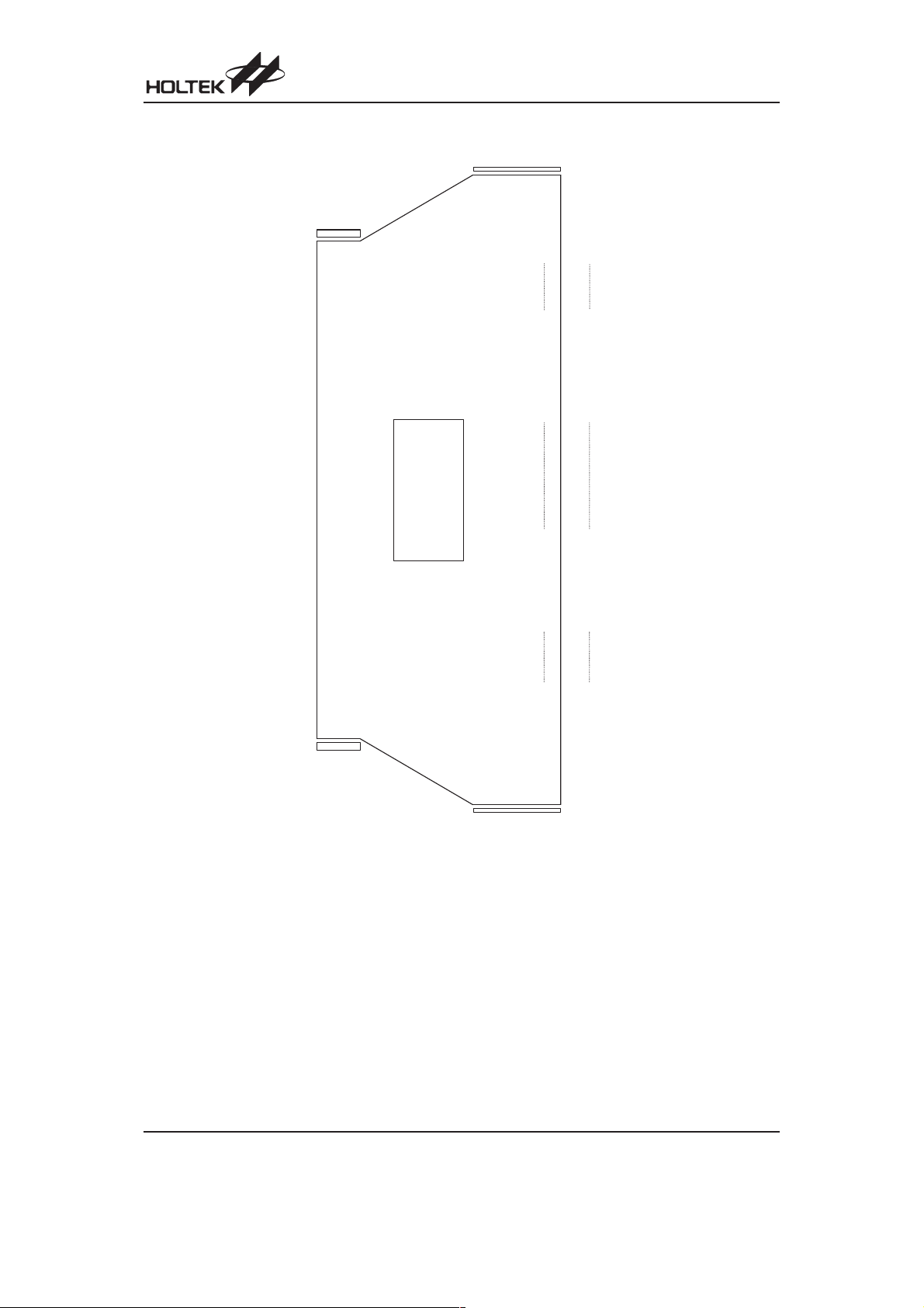
HT0610
Note:
Film: UPILEX-S 75±5mm thickness
Copper: FQ-VLP 25mm thickness
Adhesive: Toray #7100, 12±2mm thickness
Solder resist: AE-70-M11, 26±14mm thickness
Flex coating: FS-100L
Plating: Sn 0.21±0.05mm thickness
All corner radii of base film are less than 0.2mm unless otherwise noted
Other specs than display in this drawing are based on the standard spec lists
All dimensional tolerances of ²SR² are ±0.2mm unless otherwise noted
All dimensional tolerances of ²base film² are ±0.05mm unless otherwise noted
Inner lead accumulative pitch:
Output side: 9.359±0.008mm
Input side: 9.077±0.008mm
Rev. 1.10 19 April 4, 2007

Application Circuits
32/33 MUX Display with Analog Circuitry Enabled, Tripler Enabled and 1/7 Bias
T o L C D P a n e l
HT0610
M P U / M C U
w i t h
P a r a l l e l
I n t e r f a c e
R A M E P R O M
R E S
C S
C E
R W
D C O M
D 0 ~ D 7
9 1 0 k
O S C 2
O S C 1
0 . 1mF 0 . 1mF
W
C O M 0 ~ C O M 3 2
S E G 0 ~ S E G 1 1 9
A N N 1 ~ A N N 4 , B P
H T 0 6 1 0
C 1
C 2
C 1 N
C 1 P
0 . 1
3 0 0 k
V F
C 2 N
C 2 P
1 5 0 k
F
m
5 6 0 p F
W
V D D
V S S
V D D A
V L L 2
V L L 3
D U M 2
D U M 1
V L L 4
V L L 5
V L L 6
V C C A 1
V R
W
4 . 7mF
N o t e : V R a n d V F c a n b e l e f t o p e n w h e n R e g u l a t o r i s d i s a b l e d .
16 MUX Display with Analog Circuitry Enabled, Tripler Enabled and 1/5 Bias
T o L C D P a n e l
0 . 1
0 . 1mF
0 . 1mF
0 . 1mF
0 . 1mF
0 . 1mF
0 . 1mF
0 . 1mF
0 . 1mF
0 . 1mF
V
D D
F
m
M P U / M C U
w i t h
P a r a l l e l
I n t e r f a c e
R A M E P R O M
R E S
C S
C E
R W
D C O M
D 0 ~ D 7
E x t e r n a l
C l o c k
O S C 2
C 1
O S C 1
0 . 1mF 0 . 1mF
C O M 0 ~ C O M 3 2
S E G 0 ~ S E G 1 1 9
A N N 1 ~ A N N 4 , B P
H T 0 6 1 0
C 2
C 1 N
C 1 P
C 2 N
3 0 0 k
V D D
V S S
V D D A
V L L 2
V L L 3
D U M 2
D U M 1
V L L 4
V L L 5
V L L 6
V F
C 2 P
1 5 0 k
5 6 0 p F
W
V C C A 1
V R
W
4 . 7mF
0 . 1
0 . 1mF
0 . 1mF
0 . 1mF
0 . 1mF
0 . 1mF
0 . 1mF
0 . 1mF
V
D D
F
m
N o t e : V R a n d V F c a n b e l e f t o p e n w h e n R e g u l a t o r i s d i s a b l e d .
Rev. 1.10 20 April 4, 2007

16/32/33 MUX Display with Analog Circuitry Disabled
T o L C D P a n e l
HT0610
C O M 0 ~ C O M 3 2
S E G 0 ~ S E G 1 1 9
O S C 2
A N N 1 ~ A N N 4 , B P
C 1
C 2
O S C 1
H T 0 6 1 0
C 1 N
V D D A
D U M 2
D U M 1
V L L 5
V L L 6
C 1 P
C 2 N
C 2 P
V C C A 1
V F
V R
M P U / M C U
w i t h
P a r a l l e l
I n t e r f a c e
R A M E P R O M
R E S
C S
C E
R W
D C O M
D 0 ~ D 7
E x t e r n a l
C l o c k
N o t e : V R a n d V F c a n b e l e f t o p e n w h e n R e g u l a t o r i s d i s a b l e d .
V D D
V S S
V L L 2
V L L 3
V L L 4
0 . 1
0 . 1mF
V
D D
F
m
V C C
Rev. 1.10 21 April 4, 2007

Holtek Semiconductor Inc. (Headquarters)
No.3, Creation Rd. II, Science Park, Hsinchu, Taiwan
Tel: 886-3-563-1999
Fax: 886-3-563-1189
http://www.holtek.com.tw
Holtek Semiconductor Inc. (Taipei Sales Office)
4F-2, No. 3-2, YuanQu St., Nankang Software Park, Taipei 115, Taiwan
Tel: 886-2-2655-7070
Fax: 886-2-2655-7373
Fax: 886-2-2655-7383 (International sales hotline)
HT0610
Holtek Semiconductor Inc. (Shanghai Sales Office)
7th Floor, Building 2, No.889, Yi Shan Rd., Shanghai, China 200233
Tel: 86-21-6485-5560
Fax: 86-21-6485-0313
http://www.holtek.com.cn
Holtek Semiconductor Inc. (Shenzhen Sales Office)
5/F, Unit A, Productivity Building, Cross of Science M 3rd Road and Gaoxin M 2nd Road, Science Park, Nanshan District,
Shenzhen, China 518057
Tel: 86-755-8616-9908, 86-755-8616-9308
Fax: 86-755-8616-9722
Holtek Semiconductor Inc. (Beijing Sales Office)
Suite 1721, Jinyu Tower, A129 West Xuan Wu Men Street, Xicheng District, Beijing, China 100031
Tel: 86-10-6641-0030, 86-10-6641-7751, 86-10-6641-7752
Fax: 86-10-6641-0125
Holtek Semiconductor Inc. (Chengdu Sales Office)
709, Building 3, Champagne Plaza, No.97 Dongda Street, Chengdu, Sichuan, China 610016
Tel: 86-28-6653-6590
Fax: 86-28-6653-6591
Holtek Semiconductor (USA), Inc. (North America Sales Office)
46729 Fremont Blvd., Fremont, CA 94538
Tel: 1-510-252-9880
Fax: 1-510-252-9885
http://www.holtek.com
Copyright Ó 2007 by HOLTEK SEMICONDUCTOR INC.
The information appearing in this Data Sheet is believed to be accurate at the time of publication. However, Holtek as
sumes no responsibility arising from the use of the specifications described. The applications mentioned herein are used
solely for the purpose of illustration and Holtek makes no warranty or representation that such applications will be suitable
without further modification, nor recommends the use of its products for application that may present a risk to human life
due to malfunction or otherwise. Holtek¢s products are not authorized for use as critical components in life support devices
or systems. Holtek reserves the right to alter its products without prior notification. For the most up-to-date information,
please visit our web site at http://www.holtek.com.tw.
-
Rev. 1.10 22 April 4, 2007
 Loading...