

hitachi seiki Lii Maintenance Manual

t*
I
SEIKI-SEICOS
MAINTENANCE
MANUAL
LI
1995
-
4
I
1
i
I
]ÿEIKI
I
i
.
i
Hitachi

(LtieOc
'TbgN
sLBob
barosr
A
-OAJ
•T'A8/£?s
TABU'S.
&i~rg
to-
To
MTA
sÿAeej
1.
SEICOS
LI
I
BLOCK
DIAGRAM
1
1
-
»*
2.
3.
4.
2-1
2-2
2-3
2-4
2-5
3-1
3-2
3-3
3-4
3-5
3-5-1
MASTER
Check
Short
LED
General
Power
SERVO
Setting
Gain
Check
Setting
Servo
SERVO
PRINTED
Pin
Pin
Purpose
Connector
INTERFACE
Volume
adjustment
pin
Pin
Interface
Dip
SW
AMPLIFIER
and
CIRCUIT
Dipping
BOARD
Board
Setting
BOARD
Switch
.•.
Pin
2
2
2-2
2-3
2-3
2-4
3
3
3
3
3-4
3-5
3-6
4
-
1
2
-
i
-
1
2
-
2
-
-
3
;
!
!
1
-
!
5.
4-1
4-2
4-3
4-4
4-5
4-6
4-7
4-7-1
4-7-2
4-7-3
4-7-4
4-7-5
5-1
Red
Green
List
List
List
Layout
Maintenance
CRT
Appearance
Operation
LED
Operation
LED
Check
of
Adjusting
of
Jumper
of
Diagram
Maintenance
Movement
Countermeasure
Cause
and
Diagnosis
its
of
disposal
and
error
.
TerminaL
Clip
of
of
procedure
failure
of
Volume
Printed
the
for
by
deffective
servo
alarm
and
Circuit
amplifier
of
protective
output
adjustment
countermeasure
Board
Parts
function
..
4
4-2
4-3
4-4
4-5
4-5
4
-
4
-
4-7
4-10
4-12
4-13
5
-
5
-
-
1
7
7
1
1
i
5-2
5-3
Adjusting
Diagnosis
Part
of
Failure
5-2
5-2
(
)
A

u
•
6-1
Juumu
Connection
ijivi
nu
nou
with
PPR
6
-
1
6-2
Description
6-3
Method
7.
TAPE
7-1
Outline
Specifications
7-2
8.
ADJUSTMENT
Procedure
8-1
8-2
Zero
8-2-1
8-2-2
8-3
Bubble
8-4
How
9.
TROUBLESHOOT
9-1
Manual
of
READER
Return
Manual
Initial
Memory
Proceed
to
Contineous
NC
on
Transmission
FOR
TURNING
up
to
reference
(Aute
G28
Setting
the
AND
ITS
Side
the
Initial
DISPOSAL
Feed
SignaL
ON
Start-up
point
return
Procedure
is
THE
return
Disabled
POWER
of
to
Clear
System
the
.
reference
(same
of
the
for
Back-up
point)
RAM
DISK
RAM
memory)
6-2
6-3
7
7
7
8
8
8-5
8-5
8-6
8
8-12
9
9
i*
1
-
1
-
-
1
1
-
-
1
7
-
1
-
1
-
10.
11.
12.
13.
13-1
9-2
9-3
12-1
12-2
12-3
12-4
12-5
Automatic
by
Feed
DAILY
BOARD
CHANGING
MAINTENANCE
CHANGING
Ccmpatibi
NC
Data
NC
Data
NC
Data
Procedure
HOW
TO
CHANGE
Compatibility
Operation
Manual
PROCEDURES
Output
Input
Initial
Pulse
PROCEDURES
lity
of
Change
to
Clear
M16II
of
Disabled
Generator
OF
NC
Substrate
NC
Substrate
NC
SUBSTRATE
M16II
Substrate
Disabled
SUBSTRATE
of
NY
Pair
Machine
9-3
9-4
10-
11-
12-
12-
12-
12-
12-
12-
13-
13-
1
1
1
2
6
7
8
9
1
4
13-2
13-3
13-4
13-5
13-6'
Recording
Output
of
Initialization
Data
Input
Setting
of
of
AB
M16II
in
AB
Phase
Data
of
M16II
Phase
Prior
M16II
After
Current
Current
Value
to
Changing
Changing
Value
5
..
(
)
B
13-
1313-
13-
13-
7
8
9
10
.

juuJuvnn
j
ur
unmiuiiiu
i-f.
t
i\uibLfuar>
v
11
14-
1
15.
14-1
14-2
14-3
15-1
15-2
15-3
15-4
15-5
15-6
15-7
15-8
15-9
Flowchart
Setting
Adjustment
SERIES
Servo
Volume
Jumper
List
Two-shaft
Volume
Jumper
List
Abnormality
PIN/
860
SERVO
Amp.
Adjustment
Pin
Check
of
Adjustment
Pin
Check
of
Svif
of
DIP
Offset
of
UNIT
Single
For
Setting
Pins
Incorporated
Setting
Pins
Diagnosis
Substrate
Seitches
Gain
Shaft
Procedures
Procedures
(PI)
..
Procedures
Procedure
(PI)
and
Changing
(PI)
.
Type
Servo
(PI)
(PI)
.
Countermeasures
(PI)
Procedure
Amplifier
141414-
1515-
15-
15-
15-
15-
15-
15-
15-
15-
4
6
7
1
3
4
5
6
8
9
11
12
15
I
:
i
i
I
(C)

1.
SEICOS
LII
BLOCK
DIAGRAM
Battery
Bubble
Memory
I/O
Device
RAM
Serial
Inter¬
face
Master
Circuit
CPU
Prited
Board
SYSTEM
ROM
Servo
Servo
(
Interface
Board
Position
Control
Circuit
Position
Control
Circuit
I
Position
control
circuit
n
Interface
Increase)
Position
Contorl
Circuit
W
Servo
Servo
X
Amplifier
Motor
L
3
I
A
Servo
Servo
|
Z
Amplifier
Servo
IServo
C
]Amplif
ierf
Motor
Z3
z
i
Motor
•
i
3
C
t
Servo
Servo
Amplifier
Motor
nrf:
I/O
Device
Parallel
Inter¬
face
Dial
MICON
I
Port
RAM
?
CPU
162
CRT
Control
Circuit
-
SLBUS
Pssition
Contorl
Circuit
5
Key
|
Boaed
Slave
1
t
axes
?
Servo
Amplifier
Manual
Servo
CRT
Key
Pulse
Motor
Jÿxe
Board
q>
Generator
1
1
-
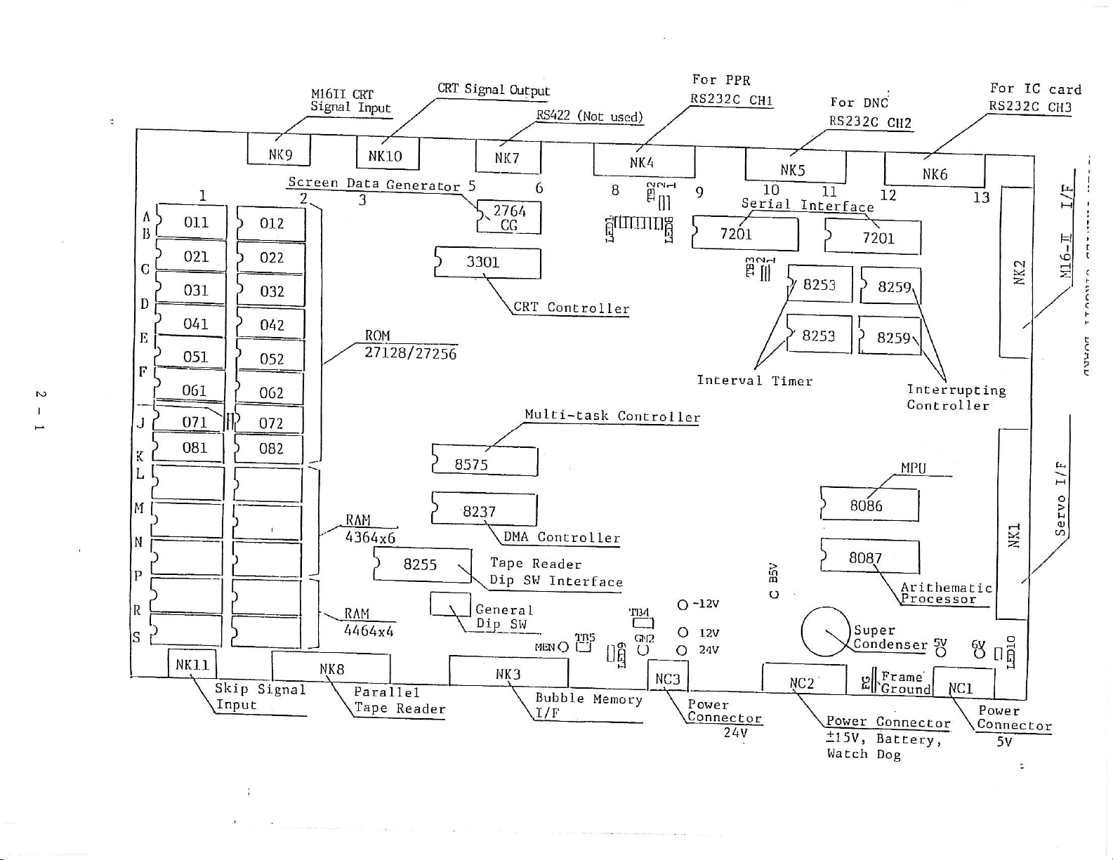
6
II
Ml
Signal
CRT
Input
CRT
Signal
Output
RS422
(Not
used)
For
PPR
RS232C
CHI
DNC
For
RS232C
CH2
IC
For
RS232C
card
CH3
5
3301
8575
8237
X
\
\
y
NK7
2764
s
CG
CRT
7
\DMA
Tape
SÿDip
Genera
Dip
NK3
6
Multi-
Reader
SW
1
SW
\
Controller
task
Controller
Interface
Tns
U
HENO
Bubble
I/F
/
NK4
8
%
graurms
9
Controller
TI34
cn
CM2
U§°
Memory
_
I
NC3
9
7201
Interval
-12V
O
12V
O
24V
O
Power
Connector
Serial
/
7
r9(NH
Bill
24V
10
y
NK5
1/
Timer
:>
m
m
O
11
Interface
8253
8253
NC2
N
Power
115V,
Watch
12
\
7201
8259
?
8259\
7
8086
8087
\
Super
Condenser
Frame
to
"Ground
Connector
Battery,
Dog
y
NK6
Interrupting
Control
MPU
ithema
Ar
Processor
5V
O
[ÿCl
13
CN
ler
H
tic
*"1
Power
Connector
5V
u-
hH
N
r
i
c
vO
I-
I
C
r
c
C
c
c
5
p
c
U-.
o
>
u
QJ
LO
/
/
NK9
Screen
A
D
£
1
Oil
021
031
041
2
012
022
032
042
E
051
P
F
K3
i
J
it
061
071
081
ii
052
062
072
082
7
NK10
Data
Generator
3
ROM
27128/27256
2
l
L
[
M
N
P
R
)
|
?
RAM
4364x6
8255
RAM
4464x4
S
t
NK11
Skip
Input
Signal
NK8
V
Parallel
Tape
Reader

2-1
Check
Pin
Name
GN
GN2
5V
B5V
12V
-12V
24V
MEN
(Note)
Substrate
lace
P
13-S
8-S
13-S
10-P
9-S
9-R
9-S
7-S
It
correct.
.
can
5V,
24V
Power
Battery
Power
Hardware
checked
be
When
B5V,
Ground
Check
Check
Check
1
tt
checking
12V,
1
Check
by
Pin
Pin
the
Pin
Contents
Ground
for
Pin
Pin
above
24V,
Pin
Check
check
use
for
GN2.
Check
pin
the
if
power
input
is
2-2
Name
TB1
TB2
TB3
TB4
TB5
(Note)
Short
Substrate
lace
P
1-J
8-B
10-C
8-R
7-S
Pin
TB2
it.
pin,
and
As
MPU
27128/27256
Both
(RS422
Both
(RS422
When
For
TB3
for
does
the
RXC
the
baut
the
maintenance
are
not
TB5,
not
Short
short
change-over)
short
rate
watch
used.
always
work.
Contents
pin
pin
pin
select)
dog
(Always
If
set
and
1
1
and
alarm
the
the
for
2
2
is
set)
short
short
change-over.
not
are
are
not
needed,
not
pin
pin.
used.
used.
has
When
27256
set
been
removing
the
set,
in
set
short
remove
this
pin.
2
2
-
2-3
Name
LED
Subs
Place
Crate
ContenCs
LED1
LED2
LED3
LED4
LED5
LED6
LED7
LED8
LED9
LED10
(Note)
8-B
8-B
8-B
8-B
8-B
8-B
8-B
8-B
8-B
13-S
LED1
LED
~
When
flickers
substrate)
When
by
It
It
It
LED9
the
always
the
flickers
flickers
flickers
Lights
Lights
software
.
fixed
This
operating,
time
at
the
the
by
by
turning
up
in
up
in
of
flickers
interruption
bubble
battery
red.
green.
the
it
on
NC
moves
by
the
flickers.
access.
alarm.
the
main
of
power.
properly,
loop.
This
50msec.
(New
is
it
flickers
flickered
2-4
General
This
RAM
NY
NY
Purpose
switch
increasing
machine
machine
is
Dipping
timed
L-side
R-side
2
1
on
substrate
substrate
substrate
Switch
3
4
OFF
by
5
the
6
7
following
Switch
Switch
Switch
8
function.
7
ON
ON
1
ON
2
2-3

2-5
Power
Connector
i*
Name
N
C
Contents
Power
1
Power
connector
No.
Pin
connector
(5V)
;!
:
6
(+15V)
5
GN
V
4
J
1
2
3
V
+5V
Substrate
N
N!
!
RDYT
(24V)
4
:i
GN2
3
cq
II
3
0)
u
u
I
2
+24V
II
-15V
11
1
1
1
2
C
C
3
Pin
Power
Pin
.
No
connector
No.
11
987654321
•
|
GN
i
NC
RDY-
1
+15V
1
1
Substrate
M/
Substrate
2-4
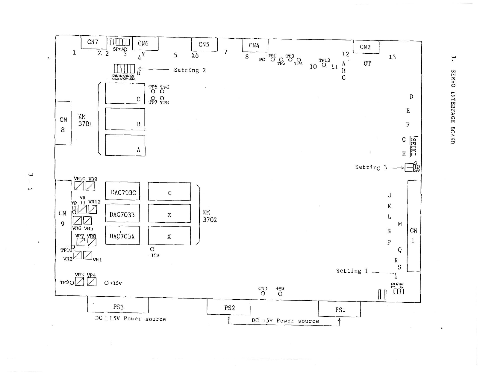
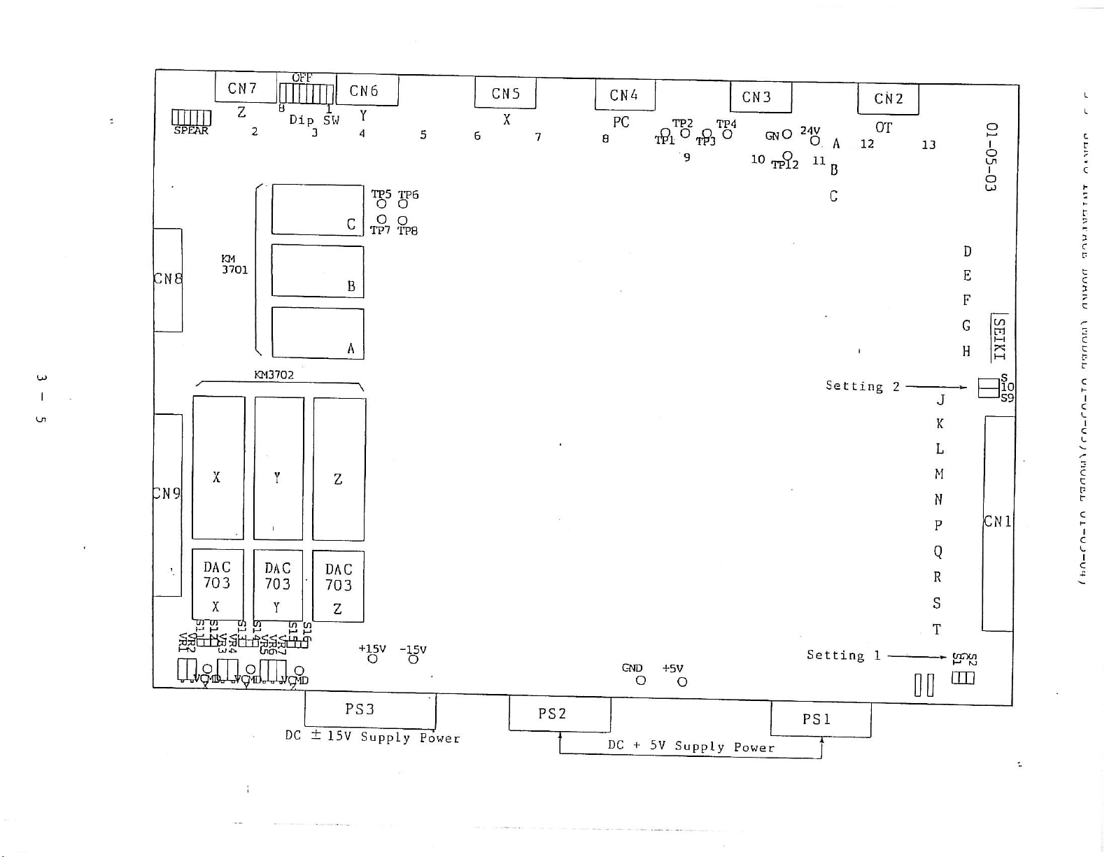
CN
8
1
CN7
KM
3701
Z
SPEAR
2
LD
cococotmom
LOÿUtn-OCD
CN6
3
Y
4
b
5
TP
o
o
c
TP7
TP6
o
o
TP8
5
Setting
D
A
X6
CN5
2
.
A
15
C
CN2
0T
13
D
E
F
c/i
G
rt
\
i
i
II
—
M
UJ
C/1
m
pa
<
o
2
H
PI
pa
>
o
PI
ta
O
>
pa
a
CNA
7
8
PC
o
T&1
TP2
'r&3
O
TP
10
TP
°
4
12
12
11
Setting
LO
I
VR10
VR9
00
VR
Wi2
I»p
11
£00
CN
00
9
VR6
VR5
vn
10
TP
00
VR2
vn
VR4
3
TP9O0
0
VR1
DC
DAC703C
DAC703B
DAC703A
M5V
O
PS
3
Power
15V
i
O
-15V
source
C
Z
X
KM
3702
PS2
.
i
DC
GND
o
+5V
+5V
o
Power
source
Setting
PS1
)
3
B&
J
K
L
M
N
P
CN
1
Q
R
1
s
l
co
cico
NJ
H*
cm
oil
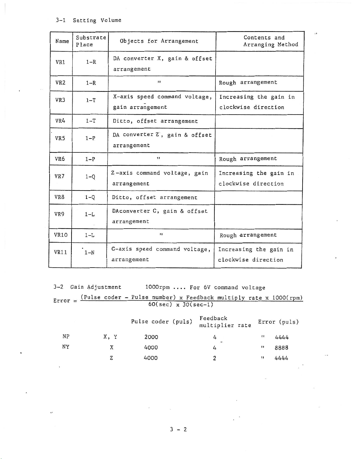
3-1
Setting
Volume
Name
VR1
VR2
VR3
VR4
VR5
VR6
VR7
VR8
Substrate
lace
P
1-R
1-R
1-T
1-T
1-P
1-P
1-Q
1-Q
Objects
converter
DA
arrangement
X-axis
arrangement
gain
Ditto,
converter
DA
arrangement
-axis
Z
arrangement
Ditto,
for
speed
offset
command
offset
Arrangement
X,
gain
11
command
arrangement
,
Z
gain
II
voltage,
arrangement
&
offset
voltage,
&
offset
gain
Rough
Increasing
clockwise
Rough
Increasing
clockwise
Contents
Arranging
arrangement
the
direction
arrangement
the
direction
and
gain
gain
Method
in
in
VR9
VR10
VR1
3-2
Error
NY
1
NP
Gain
=
1-L
1-L
1-N
Adjustment
(Pulse
DAconverter
arrangement
C-axis
arrangement
coder
X,
Y
X
Z
-
speed
Pulse
Pulse
C,
n
command
lOOOrpm
number)
60(sec)
coder
2000
4000
4000
gain
&
....
x
x
(puls)
offset
voltage,
For
Feedback
30(sec-l)
clockwise
6V
command
multiply
Feedback
multiplier
4
4
2
Rough
Increasing
arrangement
the
direction
voltage
rate
rate
Error
If
gain
IQOO(rpm)
x
If
II
in
(puls)
4444
8888
4444
3-2
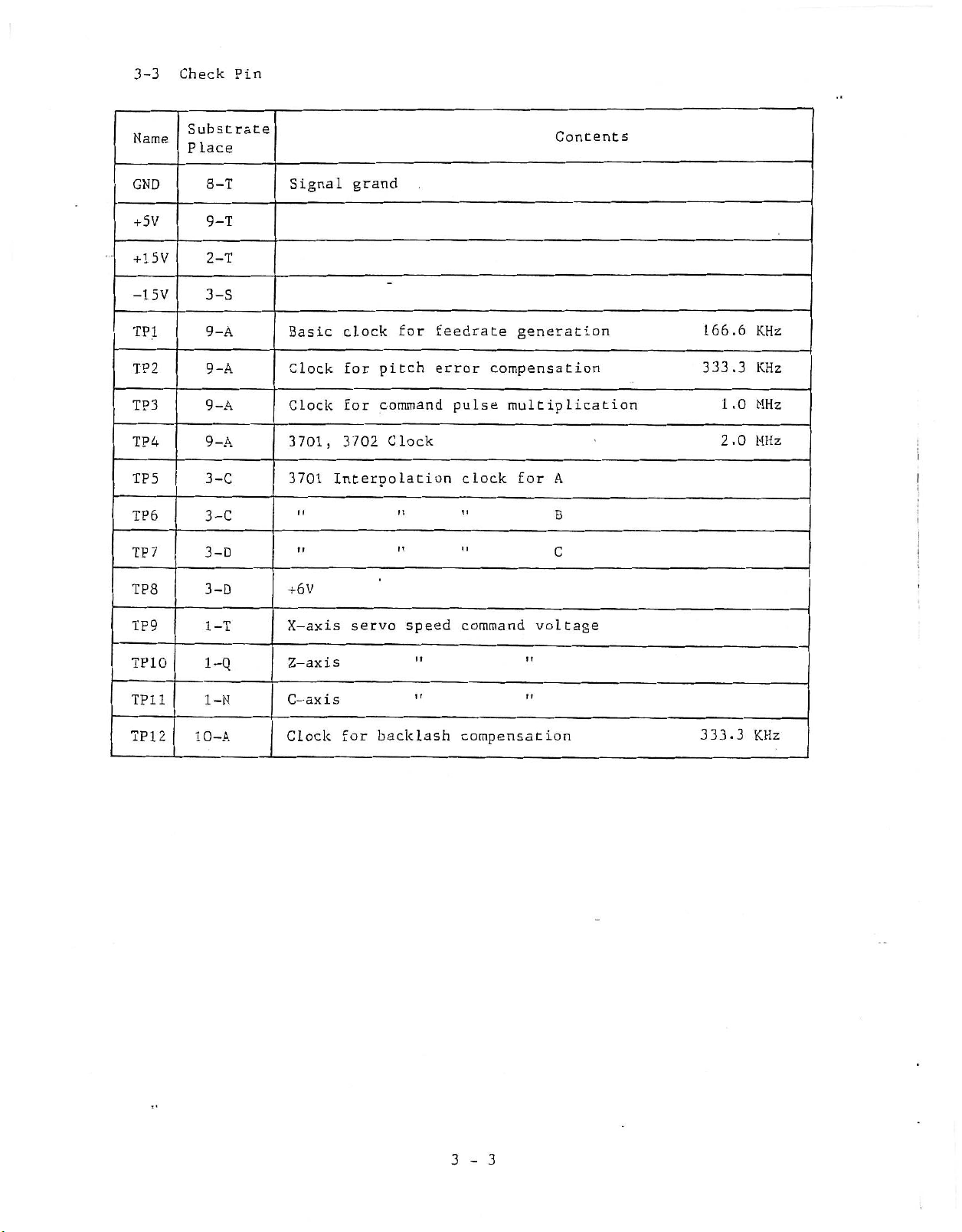
3-3
Check
Pin
Name
GND
+5V
15V
+
-15V
TP1
TP2
TP3
TP4
5
TP
TP6
7
TP
Substrate
lace
P
8-T
9-T
2-T
3-S
9
-A
-A
9
9
-A
9
-A
3-C
3-C
3-D
Signal
Basic
Clock
Clock
3701
3701
u
it
grand
clock
pitch
for
command
for
,
3702
Interpolation
for
Clock
IT
ti
feedrate
error
pulse
clock
II
n
Contents
generation
compensation
multiplication
for
A
B
C
166.6
333.3
1
2.0
KHz
KHz
.
0
MHz
MHz
I
i
'
;
TP8
TP9
TP10
TP1
TP12
3-D
1-T
l-Q
1
1-N
-A
10
+6V
X-axis
Z-axis
C-axis
Clock
servo
for
speed
1
1
1
1
backlash
command
II
tl
compensation
voltage
333.3
KHz
3-3
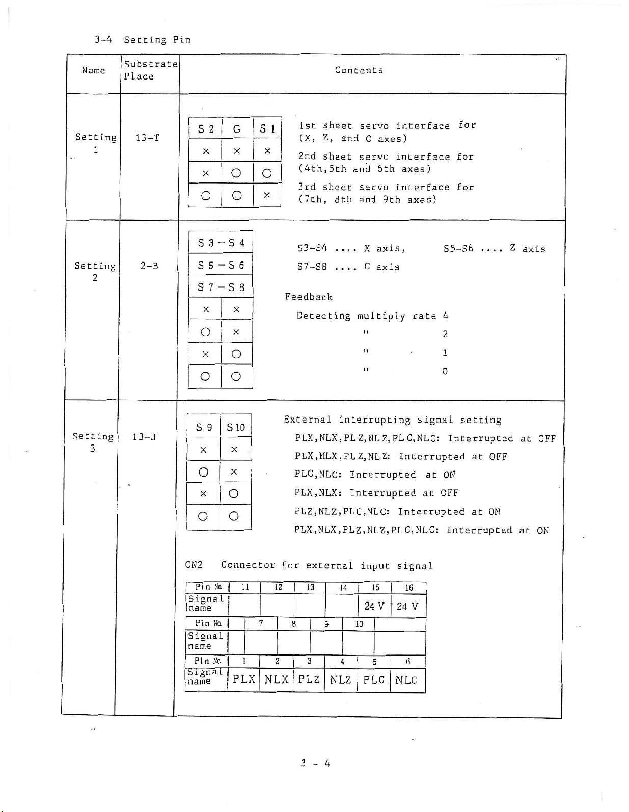
3-4
Setting
Pin
Name
Setting
1
Setting
2
Substrate
Lace
P
13-T
2-B
I
S
2
|
x
X
o
3
-
S
5
-S
S
7
-
S
x x
o
x
O
Contents
G
S
x
X
o
o
S
o
X
4
6
8
S
1
Feedback
1st
(X,
Z,
2nd
sheet
(4th,5th
3rd
sheet
(7th,
S3-S4
S7-S8
Detecting
x
o
and
8th
....
....
servo
C
servo
6th
and
servo
and
axis
X
C
axis
multiply
(f
1
1
1
1
axes)
9th
interface
interface
axes)
interface
axes)
,
rate
sheet
O
for
for
for
S5-S6
4
2
1
0
....
Z
axis
Setting
3
13-J
S
X
O
X
O
CN2
Pin
Signal
name
Pi
Signal
name
P
i
Signal
name
9
Connector
Na
No.
n
No
n
10
S
X
X
O
O
PLX
11
|
7
NLX
External
PLX
PLX
PLC,NLC:
PLX,
PLZ,NLZ,PLC,NLC:
PLX,NLX,PLZ,NLZ,PLC,NLC:
for
external
12
13
3
3
PLZ
,
,
I
NLX
MLX
NLX:
interrupting
,
PL
,
PL
|
14
9
I
I
*
NLZ
Z,
Z,
NL
Z,
Z:
NL
Interrupted
Interrupted
input
15
|
V
24
10
1
5
PLC
signal
C,
PL
NLC
Interrupted
Interrupted
signal
16
V
24
6
[
NLC
at
at
setting
:
Interrupted
ON
OFF
Interrupted
at
OFF
OFF
at
ON
at
at
ON
3-4
6
2
KM3702
uF
Dip
CN
6
Y
SW
3
4
TP5
o
o
c
TP7
TP6
o
o
TP8
5
6
CN5
X
CN4
l9l
TP2
°
T&
9
7
8
PC
TP
°
4
CN
10
3
GNO
TP?2
24V
2
CN
O
u>
o
o
Ln
I
O
11
12
A
13
OT
C
D
E
B
F
CD
G
D1
H
h-\
i
—
gfo
1
>S9
-
i
Setting
i
2
A
J
K
l.
1.
c
r
C
h
r
5
C
t
c
5
p
c
C
c
t
c
H
I
c
L
i
C
L
7
CN
z
SPEAR
KM
CN8
UJ
I
Ln
3701
L
c
c
F
tr
c
f-
I
c
l.
I
c
:N9
DAC
703
UJ
H-TO
LQsffl0
U
X
X
J
OJ-C*
y->
M
awÿo-iD
Y
I
DAC
703
Y
Lncn-ÿj
l/l
o
DC
[/}
±
Z
DAC
703
Z
PS
15V
+15V
O
3
Supply
-15V
O
Power
PS
M
N
1
p
CN
Q
R
S
T
cm
OD
cnncn
fsj
H*
GND
+5V
O
O
2
+
DC
5v
Supply
Power
Setting
PS1
<
i
1

J-b-1
(1)
U1P
SW
SETTING
ANU
DIP
bhl
SW
!
1NG
H1N
Substrate
SW
SW
SW
OFF
ON
OFF
location
1
3
5
SW
SW
SW
OFF
OFF
ON
3-A
2
4
6
Right
CN
7
X
axis
Y
axis
Z
axis
Feedback
Multiply
drawing
rt
it
8
7
detection
ratio
OFF
6
5
3
4
2
1
CN
6
4
3
2
SW
SW
ON
7
-
ON
With
ON
some
softwares,
(Used
8
-
ON
tl
ii
in
Y
axis
additional
X
axis
feedback
board
1
OFF
as
such
it
direct
tap)
3
6

(£)
blillll'Rj
t-lPI
NAME
Setting
Setting
1
2
SUBSTRATE
LOCATION
3-T
1
13-J
o
O
O
S2
X
x
S9
X
X
G
X
O
o
SIC
X
X
O
O
SI
X
O
x
Setting
For
For
For
For
For
For
DESCRIPTION
Servo
M
ft
external
PLX/
PLX/
PLZ/
PLX/
PLY/
PLX/
NLX/
interruption
NLX/
interruption
NLZ,
interruption
NLX,
interruption
NLY/
interruption
NLX/
interruption
interface
1st
2nd
3rd
PLY/
PLY/
PLZ/
PLY/
sheet
sheet
sheet
interrupt
NLY/
NLY,
is
is
NLZ,
is
NLY/
is
for
is
is
(X/Y/Z
(4/5/6
(7/8/9
PLZ/
made
made
made
made
made
PLZ/
made
signals:
NLZ
with
with
with
with
with
NLZ,
with
axes)
axes)
axes)
,
OFF.
OFF.
ON.
OFF.
ON.
ON.
CH2
Signal
Connectors
Pin
Signal
Name
Pin
Signa
Name
Pin
Name
No.
No.
No.
!
11
for
7
12
external
13
8
9
input
14
signaLs:
15
24
10
16
V
24
V
I
6
NLZ
PLX
1
NLX
2
3
PLY
4
NLY
5
PLZ
T<
3
7

.*
.
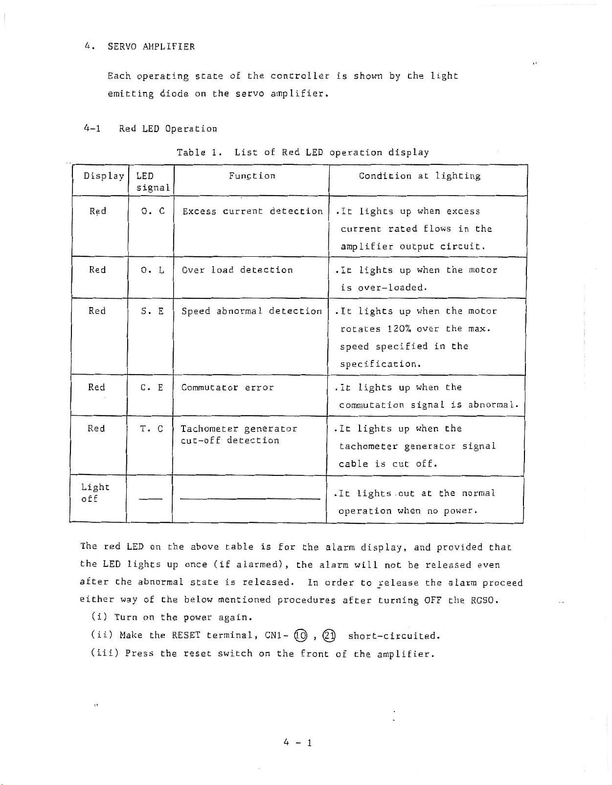
4.
SERVO
Each
AMPLIFIER
operating
state
of
the
controller
is
shown
by
the
light
4-1
Display
Red
Red
Red
emitting
Red
LED
LED
signal
0.
0.
S.
diode
Operation
Table
C
Excess
Over
L
Speed
E
on
the
1.
Func
current
load
abnormal
servo
List
ion
t
detection
amplifier.
Red
of
detection
detection
LED
operation
Condition
.It
lights
current
amplifier
lights
.It
is
over-loaded.
lights
.It
rotates
speed
specification.
display
up
rated
output
up
up
1207=
specified
at
when
flows
when
when
over
lighting
excess
circuit.
the
the
the
the
in
in
the
motor
motor
max.
Red
Red
Light
off
The
the
after
either
(i)
(ii)
(iii)
red
LED
the
way
Turn
Make
Press
C.
T.
LED
lights
abnormal
of
on
on
the
E
C
the
up
the
the
RESET
the
Commutator
Tachometer
cut-off
above
(if
once
state
below
power
reset
mentioned
again.
terminal,
switch
error
generator
detection
table
alarmed),
released.
is
is
CN1-
on
for
the
the
In
procedures
the
front
alarm
(51)
,
alarm
order
.It
lights
commutation
.It
lights
tachometer
cable
.It
lightsout
operation
display,
will
to
after
short-circuited.
the
of
up
up
generator
is
cut
when
not
release
turning
amplifier.
when
signal
when
off.
at
and
be
the
the
the
no
power.
provided
released
the
OFF
is
signal
normal
alarm
the
abnormal.
that
even
proceed
RGSO.
4
1
-

4-2
Green
LED
Operation
Display
Green
Green
Green
LED
signal
POWER
+
15
-15
Table
Power
Power
Power
2.
List
Function
receiving
receiving
receiving
of
Green
display
display
display
LED
operation
Condition
When
(AC100V,
between
up
When
+15V
CN1-Q
lights
condition)
When
-15V
CN1-®
lights
condition)
(at
the
the
is
the
is
control
50/60Hz)
and
r
normal
control
supplied
2
.
(at
up
.
control
supplied
,
®-
(at
up
.
display
at
t,
condition)
-
©
normal
©
normal
lighting
power
supplied
it
power
between
©
power
between
©
lights
,
,
.
it
it
Green
RGSO
RGSO
ON
display
lights
It
and
.
©
lights
It
rotating.
the
short-circuited
up
up
at
CN1
-
©
time
the
at
motor
4-2

4-3
List
of
Check
Terminal
Termina
code
15G
15
+
-15
V
CMD
VTG
1A
A
The
list
amplifier
Assume
Name,
1
function
OV
terminal
+15V
-14V
Speed
input
Tachometer
generator
voltage
monitor
Current
output
monitor
Commu
sensor
of
that
check
terminal
terminal
command
.
output
is
the
check
shown
the
measuring
Table
•OV
.Plus
.Minus
.For
i)
ii)
.The
return
clockwise
output
counterclockwise
i)
ii)
i)
ii)
iii)
-Commutation
phase
A
terminal
the
on
3.
for
power
checking
Low
High
output
Low
High
Type
Type
Type
table
common
List
+15V
power
speed
speed
amplifier
direction
shaft
speed
speed
of
of
of
signal
for
3.
of
Description
system
source
source
the
motor:
lOOOrpm
6V/
motor:
lOOOrpm
2V/
voltage
end
motor:
4.5V+0.
motor:
2V+0.
amplifoer
amplifier
amplifier
sensor
the
is
15G
check
control
for
for
speed
Y,
of
becomes
viewed
and
direction.
Y,
5/1000rpm
lOOOrpm
2/
output
printed
unless
terminal
control
control
command
Z,
Hand
the
minus
Z,
H
030
050
100
power
S,
D
tachometer
plus
from
polarity
S,
D
and
0.4V/A+57.
0
0.1V/A+5%
signal;
circiut
specified.
source
DC+15V+0.2V
DC-15V+0.2V
input
B
and
M
type
polarity
the
and
M
.
2V/A+5%
B
types
board
signal
types
generator
in
motor
the
in
types
the
the
of
Remarks
B
C
CK
TP1
TP2
TP9
KP
TP3
TP4
Commu
sensor
Commu
sensor
Clock
PWM
pulse
Overload
detecting
setting
Speed
setting
Speed
output
Current
amplifier
.
output
.
output
pulse
voltage
amplifier
time
output
•Commutation
B
phase
.Commutation
phase
C
.Clock
Reference
1.2MHz
.PWM
pulse
+0.2MHz
signal
Reference
2
IK
.Overload
KHz
~
Adjustable
~
amplifier
command
14V
+
+14V
.Speed
speed
0
0
signal
signal
frequency
frequency
detecting
sensor
sensor
signal
at
4-3
VR9
input
output
output
of
of
time
signal;
signal;
standard
standard
setting
voltage
amplifier
amplifier
setting
of

4-4
List
Each
But
zero
of
Adjusting
volume
the
volumes
adjustment
has
Volume
been
of
(VR1)
adjusted
the
speed
can
be
the
at
scale
readjusted
delivery
factor
(VR2)
according
from
and
to
the
servo
works.
the
amplifier
combination
VR
No.
VR1
the
of
List
of
Adjusting
function
Zero
adjustment
motors
main
and
volumes
Adjusting
•When
mand
adjust
that
rotation
to
0
(However,
be
to
using
is
Table
the
voltage
offset
the
rpm.
ignored.
conditions.
shown
4.
method
speed
com¬
is
SO
motor
approaches
drift
)
on
List
OV,
is
table
of
*
4.
volume
Variation
(-)
*
#*
/•
/
(CW)
characteristic
of
Counter-
‘’clockwise'
*
/
s
(CCW
Clockwise
'
,
/
s
VCMD
(
)
+
)
VR2
Speed
factor
adjustment
scale
•Max.
speed
clockwise
.Min.
speed
counterclockwise
direction
(In
command
the
same
voltage)
at
the
direction
at
the
C
lockwi
N
(CW)
(-)
/
/
1
*
/
/
/
t
/
A
7
/
/
/
/
/
/
/
(CCW
s
/
/
/
/
)
ei
clockwise
V.
Counter-
VCMD
)
(
+
4-4

4-5
List:
of
Jumper
Clip
Symbol
SN2
SN4
The
position
depending
jumper
Be
sure
Selection
rotating
CW,
CCW
clips
to
Name
where
upon
is
insert
of
direction
the
shown
or
Table
motor
the
jumper
specifications
as
follows:
remove
5.
List
When
the
"+"
release
When
output
input,
and
When
SN4
SN7
the
motor
polarity
the
(5)
CW
Close
and
Close
and
clip
the
of
counterclockwise
(2)
clockwise
shaft
release
is
and
clip
jumper
Description
output
input,
and
end
(T)
.
and
CCW
down
.
(3)
down
(3).
inserted
types.
after
clip
shaft
(5)
is
current
(l)
(l)
close
(Standard)
.
rotation
required
and
and
and
The
turnong
rotation
end
down
(2),
limit
(2),
(2)
is
is
viewed
and
,
to
list
off
required
for
is
and
and
be
of
the
(T)
the
close
required;
release
release
different
the
power.
viewed
for
and
from
"+"
down
majar
(D
the
polarity
(2)
(2)
from
the
and
>
motor
(2)
4-6
SN7
Current
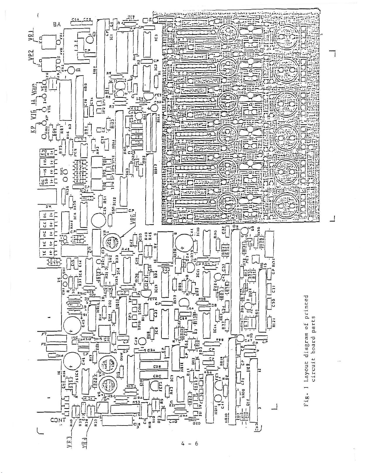
Layout
The
Fig.
Diagram
layout
1.
limit
diagram
of
When
SN4
SN7
Printed
of
the
CW
and
Close
and
Release
and
Circuit
printed
(T)
(5)
CCW
down
.
.
Board
circuit
(T)
current
(l)
and
Parts
and
(2)
board
limit
(2)
,
,
and
parts
is
and
close
not
release
shown
is
required;
down
(2)
(2)
on
4-5
I
-;
BA
q
_
“IJ
~L-J2k>
dr
6
I
C3*
%
~3
I
I
n,ÿ
L'_
"*
GS
fettsasgÿebsiKwsi
forum1
I!
if
Di
1
hl>>b
3
srOf
_lfli£rM
5.4
jflÿ
R7'
fin
....
B*i&#
3
Up
Tit
of'
5
n
0!
rirf-
WÿA,
iftfHjPyy
I
U
“
mmmm
'Mrtfiaan
Egirrÿr
lags
“SSSSML
«
i-v-5=J
<3)0
K?«S5S!3
1
n
Os
50rÿr
%
sn
U
f»
o;
PTS
®yi|»
SP§
n
SSWflP
n:.
]
ggÿOT?
soÿ-UAf
q
"ÿ
|
Llÿil
j
JQilMlW
Jioiocnoariffioÿ"”
C™T
L
I7f;'/;‘1
r
ii
3
pi
QH
~10
-
_r
6
#4:
1
B7
;'C1
P99
I
pLO1
-p|F3
*J--
jj®
ii
!
U
ns
&
”3
u
Q-
L-l
O
B
Li
00
ca
TO
U
O
03
J
QC
t-
TJ
x»
'H
*r-4
cn
i-4
CTJ
CL
LI
03
o
U
Li
U

4-7
4-7-1
Maintenace
Maintenance
of
the
servo
amplifier
Symbol
FI
FI
F2
As
on
in
dust
When
it
The
table
Type,
NCOS
NCOS
SMP
Alarm
reliable
the
servo
particular.
dirt
the
with
the
type,
6.
specification
30A
20A
10(0.1
fuse
semiconductor
amplifier,
may
not
alarm
fuse
same
specification
Fuse
Fuse
A)
Clean
be
them
thick
equipped
specifications.
Table
Q'
ty
1
1
1
elements
maintenance
periodically
and
on
and
manufacturer
6
Utsunomiya
Utsunomiya
Daito
(
BA050FXT
and
water
the
Tsushinki
,
BA030FXT
electrical
and
checking
(semi
and
oil
servo
amplifier
of
Manufacturer
Electric
Electric
Co.
annually)
may
the
Co.
Co.
)
parts
may
not
not
stay
is
are
fuse
(BA050FXT)
(BA030FXT)
are
be
so
cut
shown
employed
required
that
especially.
off,
on
replace
FI
4-7-2
10(0.
SMP
Alarm
Movement
BL
Super
abnormal
light
red
transister
alarm
status
The
cause
Release
contact
board)
fuse
signal
can
or
1A)
and
functions
status,
emitting
turns
be
of
the
input
the
procedure
is
output
identified
lighting
alarm
or
power
and
off
status
lever
1
to
when
diode
to
off.
Daito
of
protective
protect
thier
lights
be
externally.
by
and
its
by
type
Tsushinki
the
protective
up
the
interlocked
means
counter-measure
either
toggle
servo
and
The
of
the
switch
function
amplifier
the
contents
the
red
reset
Co.
function
base
status,
light
input
the
on
(BA100FXT)
and
operates,
signal
and
of
the
emitting
shown
are
(external
printed
motor
of
then
abnormal
on
circuit
the
table
from
the
main
the
diode.
the
7.
4
7
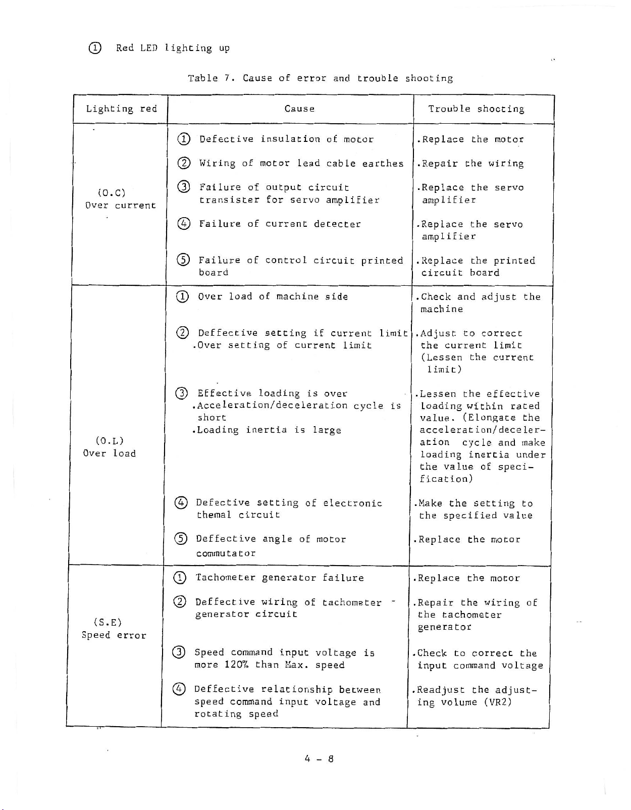
(T)
Red
LED
lighting
up
Lighting
(O.C)
Over
current
red
(T)
(2)
(3)
(4)
(J)
(T)
(2)
Table
Defective
Wiring
Failure
transister
Failure
Failure
board
Over
Deffective
•Over
7.
load
setting
Cause
of
of
of
of
of
Cause
insulation
motor
output
for
current
control
of
machine
setting
of
error
lead
servo
current
of
cable
circuit
amplifier
detecter
circuit
side
if
and
motor
current
limit
trouble
earthes
printed
limit
shooting
Trouble
.Replace
.Repair
.Replace
amplifier
•Replace
amplifier
•Replace
circuit
.Check
machine
.Adjust
the
(Lessen
1
imi
and
current
)
t
the
the
the
the
the
board
to
the
shooting
motor
wiring
servo
servo
printed
adjust
correct
limit
current
the
(O.L)
Over
(S.E)
Speed
load
error
(3)
Effective
loading
.Acceleration/deceleration
short
inertia
circuit
command
120%
setting
angle
generator
wiring
circuit
than
(4)
(5)
(T)
(2)
(3)
•Loading
Defective
themal
Deffective
commutator
Tachometer
Deffective
generator
Speed
more
input
Max.
is
of
of
is
over
large
of
electronic
motor
failure
tachometer
voltage
speed
cycle
is
.Lessen
is
.Make
.Replace
.Replace
.Repair
.Check
the
loading
value.
within
(Elongate
acceleration/
ation
loading
the
fication)
the
the
genera
input
cycle
inertia
value
the
specified
the
the
the
tachometer
tor
to
command
effective
of
setting
motor
motor
wiring
correct
rated
the
deceler¬
and
make
under
speci¬
to
value
the
voltage
of
(4)
Deffective
speed
rotating
command
relationship
speed
input
voltage
4-8
between
and
.Readjust
volume
ing
the
adjust¬
(VR2)

Lighting
red
Commutation
(l)
Cause
sensor
failure
Trouble
.Replace
shooting
the
»*
motor
(C.E)
Commutator
error
(T.E)
Tachometer
generator
disconnection
(2)
Defective
sensor
(5)
Failure
board
(T)
Disconnection
generator
(5)
Output
generator
(3)
Defective
sensor
(4)
Failure
wiring
circuit
of
sugnal
voltage
is
wiring
of
control
of
not
printed
of
circuit
tachometer
cable
for
generated
of
circuit
commutation
tachometer
commutation
printed
board
.Check
wiring
circuit
.Check
wiring
•Replace
.Check
wiring
.Replace
circuit
to
to
to
correct
the
board
correct
the
correct
the
board
the
prinred
the
motor
the
printed
1
!
»
*
4-9

4-7-3
Countermeasure
Be
sure
to
break
for
off
alarm
the
output
power
for
the
main
circuit
whenever
the
READY
When
free
loading
For
shortening
Fig.
of
shown
The
flow
follows:
signal
the
to
on
servo
continue
torque
2.
the
chart
from
amplifier
and
the
The
table
from
servo
the
running
the
by
idle
specifications
7.
occuring
Failure
speed
Set
brake
(Release
Shut
movement
RGSO
off
becomes
as
rotating
running
command
OFF
CN-
power
amplifier
alarm
as
long
time,
of
failure
occurs
v
to
21-22
T
to
speed
the
for
OV
power
becomes
state,
the
add
dynamic
to
dynamic
)
time
the
at
the
restarting
unit
off.
the
rated
alarm
dynamic
brake
motor
loading
output.
brake
resistor
operation
becomes
inertia,
circuit
is
as
is
Check
amplifier
Presume
disposal
and
5-2,
remedy
Reset
front
reset
Supply
Short-circuit
which
red
lights
cause
find
and
by
of
amplifier
or
turn
(+15VAC100V)
the
of
of
out
toggle
on
power
LED
up
'f
failure
protective
erroreous
the
v
to
of
on
switch
or
power
power
RGSO
the
make
front
by
function,
on
external
again
unit
the
points
the
of
movement
to
Restart
operation
4-10

AC
AC
210V
100V
Main
power
circuit
source
MS
Control
circuit
gniirr
*
Fig.
S
3
o
cu
__
p
«
-w
c
a
powe
Dynamic
2
r
i
brake
Servo
amplifier
circuit
!
\
rz
Motor
MS
DC±15V
to
BL8
1
2
CR
0
2
0
2
0
2
0
2
0
4
4
0
4
0
060
6
0
6
0
9
0
9
0
9
0
1
2
2
1
2
1
(
5
5
5
0
0
0
0
0
0
0
0
0
0
M
0
_L
Table
20BM-
B
H
B
B
H
D
X
S
B
H
S
M
B
S
B
p—
T
T
T
T
T
T
T
T
T
T
T
T
T
T
T
£R,
DC24V
7.
Specifications
)
BL8
0
U
0
RD
\
~
Alarm
(
27BM-
7
2
5
1
0
0
0
0
0
0
0
0
0
0
0
0
0
MOT
5
1
HOT
SQT
5
2
M
5
2
5
H
2
S
0
4
0
4
M
0
4
HOT
SQT
7
0
7
0
M
7
H
0
9
0
SOT
0
M
9
T
T
T
T
T
T
T
output
of
dynamic
Brake
)
specification
brake
resistor
0
2
0W
2
W
resistor
3.3
2.2
0.
0.
0
9
S
0
2
2
0
2
0
2
0
0
3
3
0
0
3
3
OMDT
0
0
0
0
0
0
M
BT
B
S
M
B
Z
B?
SDT
Y
Z
DT
S
T
T
T
T
T
2
3
2
330
3 3
3
4
4
4
4
6
6
6
0
0
4
1
0
4
1
0
4
1
0
2
2
0
2
2
0
2
2
HD
S
M
H
S
M
H
4-11
T
T
T
T
3
OW
1.5
0
T
T
T
3
ow
in

4-7-4
Cause
The
error
operation
of
error
caused
and
by
from
its
deffective
deffective
management
adjustment
adjustment
are
shown
on
and
the
at
its
disposal
the
table
initial
8.
Contents
Motor
OV
of
Even
command
not
attained
specified
Vibration
motor
rotating
rotates
speed
entering
voltage,
stops
.
of
command
to
value
occurs
or
Table
trouble
finely
specified
motor
the
when
is
it
8.
even
voltage
is
the
Cause
at
of
trouble
Cause
Deffective
ad
us
j
Deffective
ment
sea
le
The
Q
is
too
The
0
noise
to
input
tment
of
the
loop
increased
much.
including
influences
the
noise.
and
zero
adjust¬
speed
gain
signal
its
disposal
Disposal
Adjust
diabled
Adjust
Decrease
VR6.
Separate
signal
the
power
Make
cables
countermeasure
and
by
VR1
for
VR2
by
it
the
input
line.
wiring
and
countermeasure
(However,
.
drift)
VR3,
by
wiring
circuit
shield
with
twist
pair
VR4
of
from
cables.
J
and
the
4-12
 Loading...